Embed Size (px)
Citation preview

Chip Timing Recovery for
Indoor Wireless Networks
Employing ,J Cornmutat ion Signalling
Paul Popescu
Department of Electrical Engineering
McGill University, Montreal
Quebec, Canada
July, 1996
A project submitted to the Department of Electrical Engineering in partial fidfUment
of the requirements for the degree of Master of Engineering
@Paul Popescu, 1996

Abstract
This project considers chip timing recovery for indoor wireless networks em-
ploying Commutation Signalling. First a general analysis is made, based on the
Man'mum A Posteriori Probability (MAP) concept, which leads to a synchronizer
structure. Two cases are examined, one using a raised-cosine, the other using a
half-sine as the chip pulse. It is shown that, once acquisition has taken place and
therefore the difEerence between the incoming waveform and the locally generated
clock is of no more than a half chip duration, the synchronizer will lock onto and
track the phase of the incoming waveform.
The various blocks are implemented and the system is simulated using sirnulink@,
a system level simulator which is part of s at lab@.

Contents
1 Introduction 1
2 Derivation of t h e Synchronizer Structure Based on the MAP Criterion 7
. . . . . . . . . . . . . . . . . . . . . 2.1 Block diagram of a DBPSK modem 7
2.2 Application of the MAP criterion . . . . . . . . . . . . . . . . . . . . . . 10
. . . . . . . . . . . . . . . . . . . 2.3 Practical implementation approximations 13
. . . . . . . . . . . . . . 2.4 Analysis of the proposed convergence algorithm 14
2.5 Proposed structure for the synchronizer . . . . . . . . . . . . . . . . . . . 17
3 Convergence for Specific Waveforms 19
3.1 Codewords and codewords autocorrelations . . . . . . . . . . . . . . . . . 19
3.2 Codewords autocorrelation functions - raised-cosine case . . . . . . . . . 21
3.3 Convergence in the raised-cosine case . . . . . . . . . . . . . . . . . . . . 24
3.4 Codewords autocorrelation functions -- half-sine case . . . . . . . . . . . 26
3.5 Convergence in the half-sine case . . . . . . . . . . . . . . . . . . . . . . 31
4 Block-Level Implementation and Simulations 33
. . . . . . . . . . . . . . . . . . . . . . . . . . . . . . 4.1 Circuit description 33
4.2 Simulation results . . . . . . . . . . . . . . . . . . . . . . . . . . . . . . . 36
4.3 Implementation without carrier phase tracking . . . . . . . . . . . . . . . 40
5 Summary and Conclusions 45
A Details of the Building Blocks
. . 11

References

List of Figures
. . . . . . . . . . . . . . . . . . . . The Commutation Signalling Process 3
The DBPSK Commutation Signding Block Diagram . . . . . . . . . . . 7
. . . . . . . . . . . . . The DBPSK Commutation Signalling Modulator 8
The DBPSK Commutation Signalling Demodulator . . . . . . . . . . . . 9
. . . . . . . . . . . . . . . . . . . . . . . . . . . . . Synchronizer structure 18
. . . . . . . . . . . . . . . . . . . . . . . . Raised-cosine autocorrelation 22
Codeword 10110 autocorrelation . raised-cosine chips . . . . . . . . . . . 23
Codeword 10001 autocorrelation . raised-cosine chips . . . . . . . . . . . 23
Codeword 11110 autocorrelation . raised-cosine chips . . . . . . . . . . . 24
. . . . . . . . . . . . . . . . . . . . . . . . . . . Half-sine autocorrelation 27
. . . . . . . . . . . . . . Codeword 10110 autocorrelation . half sine chips 30
. . . . . . . . . . . . . . Codeword 10001 autocorrelation . half sine chips 30
. . . . . . . . . . . . . . Codeword 1 11 10 autocorrelation . half sine chips 31
. . . . . . . . . . . . . . . . . . . . . . . . . . Testbench for Synchronizer 35
. . . . . . . . . . . . . . . . . . . . The wave at the input of the channel 37
. . . . . . . . . . . . . . . . . . . . . . . The direct wave and its replicas 37
. . . . . . . . . . . . . . . . . . . . The wave at the input of the receiver 37
. . . . . . . . . . . . . . . . . . . . The synchronization process -- case 1 38
. . . . . . . . . . . . . . . . . . . . . The synchronization process case 2 39
. . . . . . . . . . . . . . . . . . . . The synchronization process -- case 3 39
. . . . . . . . . . . . . . . . . . . . . . The synchronizer -- envelope case 41
iv

. . . . . . . . . . . . . . . 22 The synchronization process -- envelope case 42
. . . . . . . . . . . . . . . . 23 The synchronization process multiplier case 43
. . . . . . . . . . . . . . . . . . . . . 24 The synchronizer -- multiplier case 44
. . . . . . . . . . . . . . 25 3 Waveform Generator Filter Impulse Response 47
. . . . . . . . . . . . . . . . . . . . . . . . 26 3 Waveform Generator detail 49
. . . . . . . . . . . . . . . . . 27 3 Waveform Generator . Generating filter 49
. . . . . . . . . . . . . . . . . . . . . . . . . . . . 28 Counter block . detail 50

1 Introduction
The word synchronow comes from the Greek sunkhronos (sun, with, and khronos, time),
meaning two actions happening at the same time. Therefore, to synchronize means to
cause two events to occur at the same time or to proceed at the same rate.
Synchronization is a very important aspect of a digital communication system. In a
digital'communication system, a set of symbols of predetermined duration and shape,
representing the message to be conveyed, are transmitted from one point to another.
In the process of transmission, the shape of the symbols may be altered, there may be
various additive disturbances, or the time base may be unknown. The receiver has the
task of processing these distorted symbols in such a way as to detect (recover) the original
set of symbols.
Sigdicant time and effort has been spent to investigate the problems related to
optimal detection of the symbols; there is a great deal of literature studying the effects of
fading, multipath and intersymbol interference in the context of white Gaussian additive
noise. A common assumption of literature in this area is that the receiver has a proper
time base (it knows the epoch and duration of the chips or symbols). But, in order for
this to be so, synchronization must have been achieved.
Often, the information in a digital system appears serially in a time multiplexed
form. The information can be encoded in the form of pulses representing chips, which
are grouped to form bits; the bits can further be grouped to form words, which can in
turn be grouped to form frames, etc.
For the receiver to properly process the received information, it is necessary that it be
1

able to correctly identify the beginning and duration of each pulse, bit, word and frame.
The process of identification is called timing synchronization of the receiver.
A type of channel that received - and continues to receive - increased attention due
to its practical importance, is the wireless (multipath fading) channel. Unlike the wireline
channel, the wireless channel is characterized by the existence of several propagation
paths from the transmitter to the receiver: the transmitted wave is reflected by the
buildings, trees, hills in the outdoor environment; or by walls, floors, ceilings, furniture
in the indoor environment. The waves arrive at the receiver on different paths of unequal
lengths and therefore with different delays and random phase shifts. This phenomenon
is called "multipath", and the superposition of the waves reaching the receiver leads
to either constructive or destructive addition, depending upon the relative phase shifts
between the waves. Where the addition is destructive, the resulting signal can be very
small, and this is called "fading".
Due to the unequal delays of propagation, replicas of one pulse may very well reach the
receiver after the following pulse amved at its destination, or a t the same time, making
it very hard to reliably determine whether this represents a new pulse, or a replica of
a previous one, or even to distinguish them: this is called "intersymbol interferencen
(ISI). The time interval after which there are no more replicas of a transmitted pulse
on the channel (ringing) is called "multipath delay spread"; in the outdoor environment
it can be of the order of several tens of microseconds, while in the indoor environment
it can be of the order of hundreds of nanoseconds. The main obstacle to achieving
high transmission rates on such a channel is the intersymbol interference induced by the

multipath phenomenon. When the multipath delay spread of the channel is larger than
the duration of a channel symbol, IS1 results. In the presence of ISI, the task of decoding
the channel output symbol by symbol is difficult. For such a decoding strategy to work,
the channel must bemade to appear as if the transmission of each symbol occurs in
isolation from all previous and successive symbols.
Among the approaches that have been considered for the purpose of overcoming IS1
are adaptive equalization techniques and commutation signalling. Adaptive equalization
is a subject widely treated in the literature and will not be discussed in this project.
Commutation signalling was introduced by Turin in [6]; it is the approach examined in
this project.
Commutation signalling is a bandwidth expanding modulation which is robust to
multipath induced ISI, and makes possible the exploitation of time diversity inherent in
this propagation medium. An N x M commutation signalling system uses M signal sets,
each with N waveforms. Its functionality can be explained with the help of Figure 1: let
Symbol 1 Symbol 2 Symbol 3 Symbol M Symbol Mt1 Symbol M t 2 Set 1 Set 2 Set 3 Set M Set 1 Set 2
Figure 1: The Commutation Signalling Process
the channel multipath delay spread be Tc and the symbol duration, Ts, such that M =

121 , where [(-)I denotes the nearest integer larger than (.); the bit rate of the data source
is R, and N is chosen large enough to be able to support this bit rate. Provided that the M
signal sets have very small inter-set partial correlations, a communication strategy which
allows for the separation of successive symbols over the channel can be implemented:
the source bit stream is divided into several lower rate bit streams, modulated using
waveforms from different signal sets in a round-robin fashion - ideally those would -
be mutually orthogonal waveforms, uncorrelated under any time shift - and then is
recombined, converted to passband and sent over the channel.
The 2 x M commutation signalling scheme is optimal in the sense that it uses the
minimum number of waveforms (actually, the number of signals used can be further
halved by using bipolar modulation such as Binary Phase Shift Keying, BPSK, or Differ-
ential Binary Phase Shift Keying, DBPSK). To illustrate this optimality, let us consider
two signalling schemes operating at the same bit rate, R: 2 x M bipolar commutation
signalling (e.g. DBPSK) and M-ary signalling (e.g. M-FSK). In the first case, since
1 R = 7, where Ts, is the signal duration, it follows that the number of sets, MI, neces
IS1 due to channel ringing, T,, = Tc, where Ts, is the signal duration; if the number of
waveforms is now M2, the bit rate is R = 10g2(M2). Therefore, in order to achieve the Tc
same bit rate R, M2 must be equal to 2M1, i.e. we need now 2Ml signals.
An advantage of 2 x M commutation signalling using DBPSK is the fact that it does
not require a phase reference, hence allowing for differentially coherent detection, which
offers a 3dB signal-to-noise ration (SNR) advantage, compared to orthogonal M-FSK.

Indoor wireless systems have been proposed t o operate at data rates of the order of
40Mb/s/channel. The receiver, and specifically the synchronizer, must be implementable
in a combination of high-speed analog and high-speed digital circuitry for such a data
rate (and an even higher chip rate). This means that the synchronizer structure should
be chosen t o be compatible with the IC technology.
The problem of synchronization at different levels (chip, bit, word, frame, etc.) has
been studied in literature: F'ranks [12] and [2] studied a pulse amplitude modulation
(PAM) timing recovery method based on the Maximum Likelihood (ML) criterion, which
leads to a likelihood function to be maximized. Meyers and F'ranks [13] studied the joint
carrier phase and symbol timing recovery for PAM systems. In [9], Pickholtz et al.
studied both acquisition and tracking, at the chip level, of a classical spread-spectrum
system. The same study can be found in [3] (pp. 562-570), and a similar one in [I]
(pp. 159-165); also in [I] (pp. 428-435) a serial symbol synchronizer based on the MAP
criterion is derived.
We have not seen a treatment of the problem of synchronization in commutation
signalling in the standard literature. Although this technique was proposed in 1984, it is
only recently that it has been studied in depth, after it was recognized that it offers a low
complexity solution to the problem of IS1 induced in the indoor wireless environments.
This project investigates the problem of chip synchronization appropriate for indoor
wireless networks operating with commutation signalling. Its original contribution lies is
the fact that, based on the MAP criterion, it derives a structure of a chip synchronizer
for a modem operating with commutation signalling. The job of the synchronizer is to

provide sample points once per chip, such that reliable decisions can be made from the
sample values. The specific commutation signalling scheme considered here uses DBPSK
with differential coherent detection at the receiver.
The project is structured in the following manner: in Section 2 a structure of syn-
chronizer based on the MAP criterion is derived. In Section 3, the convergence of the
proposed algorithm for pulses having a raised-cosine shaped spectrum and for half-sine
shaped pulses is examined. In order to prove the concept, the synchronization system is
implemented and simulated for half-sine pulses in Section 4. Two alternate synchronizer
configurations, that do not need carrier phase tracking, are also presented in this section.
Finally, details of some of the blocks used to build the system in sirnulink@ are presented
in the Appendix.

2 Derivation of the Synchronizer Structure Based on
the MAP Criterion
2.1 Block diagram of a DBPSK modem
In this section we will derive a structure for the synchronizer based on the MAP criterion.
We start by describing the DBPSK modem in Section 2.1, then proceed with the math-
ematical derivations that lead us to an expression to be optimized in Section 2.2. We
continue with some practical implementation considerations in Section 2.3, the analysis
of convergence of the proposed algorithm in Section 2.4 and end up with a structure of
synchronizer in Section 2.5.
The scheme considered in this chapter is an implementation of 2xM commutation sig-
nalling, using bandwidth spread DBPSK signals. Its block diagram is shown in Figure 2.
Source
1 Processor C, L- I Processor I
Figure 2: The DBPSK Commutation Signalling Block Diagram
7
v Multipath
Fading Channel
.
e Rake
DBPSK Coq~u@tion p g odulator
- Matched Filters Estimator Bank
and

The M commutation signal sets consist of M short chip sequences, selected in such
a way as to have good shift and cross-correlation orthogonality.
In Figure 3 it is shown the DBPSK commutation signalling modulator. The source
data is differentially encoded and then multiplied by the commutation signalling code-
words, used in sequence (the commutation signalling codewords are, in turn, modulated
by a spectrum formatting waveform, such as raised-cosine pulse or half-sine pulse, not
shown in the figure); the resulting waveform is then converted to passband and trans-
mitted over the channel.
Source Bit
I Generator I
To Carrier
Figure 3: The DBPSK Commutation Signalling Modulator
Figure 4 shows the DBPSK commutation signalling coherent differential demodula-
tor for the case of three shift-quasi orthogonal waveforms; it consists of a bank of filters
Modulator Commutation
Code wv I I
I
I 1 g .(t)

matched to the commutation signals, followed by delay, conjugate and multiply blocks,
the output of which are combined by a RAKE processor1 with activated taps corre-
sponding to the channel multipath delays (the multipath delays can be estimated from
the matched filters outputs). The RAKE processor is usually implemented as a digital
delay line which entails sampling its input. Synchronization provides the RAKE pro-
cessor with the correct sampling instants and therefore with the correct sample values
needed for making a decision.
Figure 4: The DBPSK Commutation Signalling Demodulator
Variable
The "RAKE processor" is a structure that contains a tapped delay line, with taps spaced at intervals of a chip duration; it attempts to collect the signal energy from all the received signal paths that fall within the span of the delay line and carry the same information.

2.2 Application of the MAP criterion
At the beginning of our analysis, we will make the assumption that the carrier phase is
known at the receiver (the receiver employs carrier phase tracking2); then, in Section 4.3,
we will show how, with minor modifications, the scheme derived here can be used without
carrier phase tracking.
Let us consider the wave present at the input of the receiver due to a single path.
The incoming wave, in baseband representation, has the form
where n(t) is white Gaussian noise with (double sided) power spectral density No, x(t; r )
is the signal and where T is the delay versus a certain reference (the same reference
being used also by the locally generated clock). The signalling interval (known at the
receiver) is T, and the observation interval, To, is of K symbols, To = K . T ; during
this interval it is assumed that the delay, T , remains constant. We assume there are
M signalling quasi-shift orthogonal waveforms, go(t) . . . g ~ - l (t) , used in this order, and
that the information bits, bk , are known during the preamble (training period). We can
then write:
where [kIM means "k modulo M". By choosing a convenient complete orthonormal basis
2
This assumption is needed in order for the synchronization problem to be mathematically tractable.

{$j) to represent z(t) we have:
K-I = bkmMi+ni , i = 1 , 2 , - - -
Let z = [zl Q . . .lT. ; then, according to the MAP criterion, the value of r which maximizes
the probability density function (pdf) p(r 1.) is the estimate of the delay. Making use of
Bayes' relation, we have:
Let zN = [z1z2.. . zN] ; the variables z; are Gaussian independent identically distributed K-1
(iid), having the mean bkgIkIMi and variance No, and therefore we have: k=O

and since p(r ) is constant over a symbol interval and
it follows that:
N K-1 2 N K-1 ( XI E b k g ~ ~ l i=l k=O J_{fiEzi E b k g h l M i ~ ( T ~ z N ) = const. exp - i=l k=O
2No No
In the above expression the first exponential ,represents the energy of the transmitted
signal, and does not depend upon r , and thus only the second exponential influences
the decision; we have:
and thus, the likelihood function that must be maximized is:
which further, by letting N + oo , becomes:

where:
2.3 Practical implementation approximations
In order to implement this relation in practice, the observation interval, To , is assumed
to be very long compared to the symbol duration, T , and then the integral is taken from
-oo to oo . With those approximations, it follows that
We can use the derivative of i(+) as a control voltage to adjust the delay:
1. A(+) = max , A(+) = 0, and the frequency (and phase) of the local oscillator
remains unchanged;
2. -A(?) < 0, which will determine a momentary decrease in the local oscillator's
frequency, leading to an increase of .i;
3. -A(?) > 0, which will determine a momentary increase in the local oscillator's
frequency, leading to a decrease of +.
Therefore, in the first case the local phase remains unchanged (i.e. the estimate is good)
while in cases 2 and 3 the phase is adjusted so that the local oscillator gets synchronized
with the incoming wave. The voltage controlled clock (VCC) by its integrating effect,
13

will approximate the sum appearing in the formula of A(?) ; we can then use as control
voltage vk, where
with the dot indicating differentiation e t h respect to the whole argument.
2.4 Analysis of the proposed convergence algorithm
In order to analyze the convergence of the algorithm based on the control voltage vk , we
consider the case where the channel noise is zero; then
and
and since the sequences g[k], are shift-quasi orthogonal and real, it follows that

where RgLkly represents the time autocorrelation of the signalling function gikIM3.
Now, let us consider the clock locally generated by the VCC, delayed by .i with respect
to a certain reference (the incoming wave is supposed to be delayed by T with respect to
the same reference); the instantaneous phase of the clock is:
which implies that
6 = wo(l - .i)
The VCC operates according to the equation:
where oo = 2r/T and K, is the gain of the VCC. Therefore, for t E [kT, (k + l)T) , we
have:
3
The w sign was used instead of the = sign, since in order for this relation to be exact, the integral should extend from -00 to oo.

Applying this last relation to our case, we have:
To demonstrate the convergence of the algorithm based on this expression is quite a
difficult task; on the other hand, by using a simplified expression, the convergence near
the point .i = T can be demonstrated. For this, we use the fact that in the vicinity of
their maximum, all three autocorrelation functions, RgfklM, m y almost identically; then,
EQ. 13 simplifies to:
where we denote by Rg the unique autocorrelation function approximating the three
autocorrelation functions. It is immediately apparent that in the cases where Rg is a
smooth function of .i in the vicinity of r , it has a unique extremum (maximum) and
provided the multiplicative constant in the right hand of the above equation is properly
selected, this iterative method will converge towards the actual value of the delay, fk + T.

2.5 Proposed structure for the synchronizer
In order to implement a synchronizer structure based on the expression obtained for vk,
we need to rewrite it in a different, but equivalent, manner; by noticing that4
and therefore
we can rewrite the control voltage as
which leads to the synchronizer structure illustrated in Figure 5.
The sample-and-hold blocks are needed to insure that the "ringing" (replicas of the
same bit arriving delayed to the receiver due to multipath) does not influence the control
voltage of the VCC during the symbol period, T. The decision block is the one that per-
forms coarse synchronization (acquisition) up to an accuracy of f Tc/2 and then presets
the timing block (a cyclic counter) to start its operation from the position corresponding
to the specific code of the sequence arriving at that particular time.
4
The sign 8 means "convolutionn


3 Convergence for Specific Waveforms
3.1 Codewords and codewords autocorrelations
Prior to investigating the convergence of the algorithm for specific waveforms used to
shape the chips, we need to calculate the general expression of the signalling waveform
autocorrelation as a function of the pulse autocorrelation. In order to demonstrate the
concept, three codewords of length five each (i.e. 5 chips per codeword) are used, which
are sufficient to overcome the channel multipath delay spread; the codewords with the
best properties in terms of orthogonality were found to be: 10110, 10001 and 11110. 4
Let gl (t) = q,r p(t - iTc) be one signalling waveform, where I = 0,1,2, q~ are the id
chips and p(t) is the chip shaping waveform; then
The autocorrelations are, in order:
1. Codeword [10110]: co = -1, cl = 1, c2 = c3 = -1, c4 = 1, and after a few simple
mathematical operations, we get:

2. Codeword [10001]: Q = -1, cl = c2 = c3 = 1, c4 = -1, leading to:
3. Codeword [11110]: Q = cl = q = Q = -1, q = 1, leading to:
Using the above results, we will further investigate the convergence when employing
the following chipshaping waveforms:
1. raised-cosine pulses;
2. half-sine pulses.

3.2 Codewords autocorrelation functions - raised-cosine case
We will start by deriving the codewords autocorrelations in Section 3.2, and then proceed
to examine the convergence of the synchronization algorithm for the raised-cosine case
in Section 3.3.
The expression of a pulse having a raised-cosine spectrum is:
where the 'koll-off factor" P E [O,l]; the Fourier transform of this pulse is:
else.
and its power spectral density is:
1 - P for 0 5 I f 1 < -- 2Tc '
1 1 - P l + P
P P 2Tc 2Tc , for-<If]<-;
(0, else.
Since the autocorrelation is the inverse Fourier transform of the spectral power density,

G(9) = Irn S(f) exp(j2n f 9)df, after some straight, albeit tedious, calcul?tions, we get: -00
sin [n(i - PI;] + g . sin [n(1 +PI;] h ( 8 ) = Tc. 0 8 9
47r- - 0.25 sin (T8$) ms (7r;) (7)' - (Pn@
9 9 The graph of this expression is plotted in Figure 6 as a function of -, where - E [
Tc Tc
for ,O taking the values 0.1,0.3, . . .0.9.
Based on Eq. 20, we can further calculate and plot the autocorrelation functions
-01 -0.8 -0.6 -0.4 -02 0 0.2 0.4 0.6 0.8 1 O/Tc
Figure 6: Raised-cosine autocorrelation
-1,lI;
of the

three codewords (Figure 7, Figure 8 and Figure 9 respectively):
01 G
Figure 7: Codeword 10110 autocorrelation - raised-cosine chips
Figure 8: Codeword 10001 autocorrelation - raised-cosine chips

Figure 9: Codeword 11110 autocorrelation - raised-cosine chips
3.3 Convergence in the raised-cosine case
As can be seen, the three autocorrelation functions behave in a similar manner (i.e., their
derivatives are almost equal) around the point 8 = 0, and they have only an absolute
maximum, at 8 = 0, so the algorithm will converge. To demonstrate this, we will
approximate RblM(e) with 5 Rp(0); also, in the vicinity of 0 = 0, we will develop the
A e sine and the cosine in Taylor series and keep only the relevant powers of x = -, with Tc
the result that:

This relation can be further simplified by discarding the terms in x2 from the denomina-
tors, leading to the following expression for the simplified raised-cosine pulse autocorm-
lation:
It follows that
A 7r2 7r2 6 - 7r2 where f (P) = - - - - P + (7r2 - 8)p2 + -
3 4 12 P3, and therefore
which in turn leads to
A K" where B = 207r- . f (P). w," . T,

By applying the z-transform to Eq. 23, we get:
where 7 A Z ( i k ) . For the above to converge, the condition is that the unit-circle be
included in the region of convergence, i.e. 11 - BI < 1, which sets an upper limit on K,,
the VCC gain; the solution is then:
Therefore, when the condition on B (or equivalently, on Kv), is W e d , .ik -+ r , which
means that the algorithm is convergent for pulses with raised-cosine shaped spectrum
and the system synchronizes, once capture has taken place.
3.4 Codewords autocorrelation functions - half-sine case
Using the same procedure as in the previous section, in Section 3.4 we will calculate
the codewords autocorrelations in the half-sine case, followed by an examination of the
convergence algorithm in Section 3.5.
We start from the mathematical expression of the half-sine pulse:
I 0, else.

Its autocorrelation function is:
and is plotted on Figure 10.
Figure 10: Half-sine autocorrelation
Since the pulses are time limited to a period of Tc, it follows that &,(Of n.Tc) = 0 for
n > 1. Therefore, the only nonzero terms in the signaling waveforms' autocorrelations

are, in this case, Rp(B) and G(B f T,); we have:
, for 0 E [-Tc,O];
1. Codeword [10110]: c,, = -1, cl = 1, q = c3 = -1, c4 = 1:
I sin (;) 2
cos 7r- + 3 . - 5 . 3 - ( :c) :[ . - c- (T:)], for 0 E [O,T~];
% 1 c
(26) Tc 5. -. - cos (.$)], for 8 E [-Tc,O]; 2
1 c else.
2. Codeword [10001]: Q = -1, cl = c2 = c3 = 1, q = -1:

3. Codeword [11110]: q, = cl =. c2 = q = -1, Q = 1:
- -
The autocorrelations are plotted in Figure 11, Figure 12 and Figure 13, respectively.
t
5 . - . cos 7r- + 5 . - Sin (4) Tc 2 (:) :[ 7r- 0 - cos (7r@], for O t [O,Tc];
Tc
Sin (G) (27) T c 5 - c ( 7 r ) 2 - 4 0 - cos (+)], for 0 t [-T., 01;
7r- Tc
\ 0, else.

e/r,
Figure 11: Codeword 10110 autocorrelation - half sine chips
Figure 12: Codeword 10001 autocorrelation - half sine chips

Figure 13: Codeword 11110 autocorrelation - half sine chips
3.5 Convergence in the half-sine case
In order to prove the convergence of the proposed algorithm around the point 0 = 0 (or
f = r) , we will use the same kind of approximation that we used for the raised-cosine
case, i.e. we'll approximate R,(x) with 5 . &(x):
Tc sin (7rx) 5 2- -cos(nx) + 5 - - x - Tc 2 [ 7rx
- cos(7rx) , for x > 0;
Tc sin (TX) 5. - .cos(7rx) - 5. - . x . 2 Tc 2 [ 7rx
I - cos(7rx) , for x < 0; I

We further differentiate Rg with respect to i, and get:
which, for 0 close to 0 gives:
This in turn leads to:
A 5n3 where A = - . Kv. Again, the condition of convergence imposes that 11 - A1 < 1,
w; , Tc
therefore an upper limit on A, or, equivalently, on K,.
4 Block-Level Implement at ion and Simulations
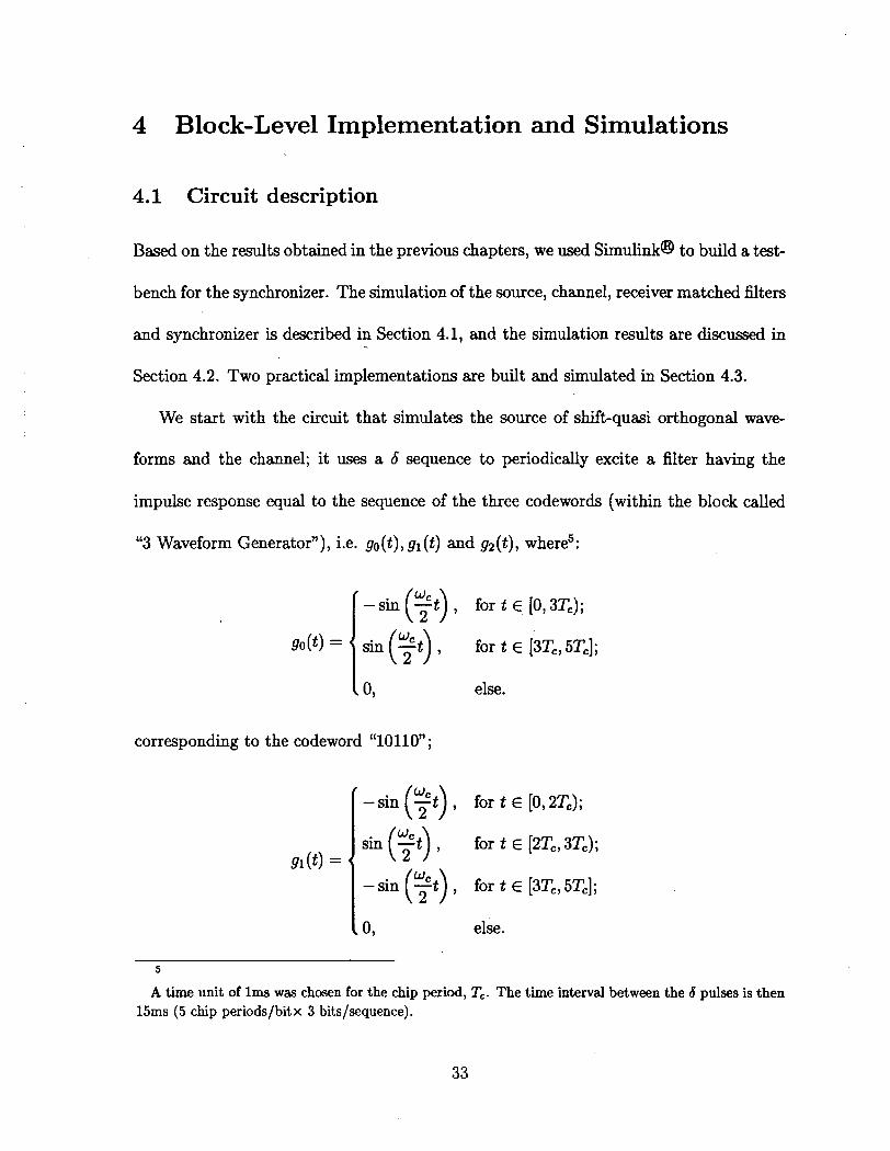
4.1 Circuit description
Based on the results obtained in the previous chapters, we used ~imulink@ to build a test-
bench for the synchronizer. The simulation of the source, channel, receiver matched filters
and synchronizer is described in Section 4.1, and the simulation results are discussed in
Section 4.2. Two practical implementations are built and simulated in Section 4.3.
We start with the circuit that simulates the source of shift-quasi orthogonal wave-
forms and the channel; it uses a 6 sequence to periodically excite a filter having the
impulse response equal to the sequence of the three codewords (within the block called
"3 Waveform Generator"), i.e. go(t), gl (t) and gz (t), where5:
[ - s ( t ) , for t E [0,3Tc);
% (t) = { sin (2t) , for t E [3Tc, ST.];
corresponding to the codeword "10110" ;
[ - sin ( t ) , for t E [0,2Tc);
sin (7t) , for t E [2Tc, 3Tc); 91 (t) =
- sin (:t) , for t E [3Tc, 5T.I;
5
A time unit of lms was chosen for the chip period, Tc. The time interval between the 6 pulses is then 15ms (5 chip periodslbitx 3 bits/sequence).

corresponding to the codeword "10001"; and
( - sin ( 2 t ) , for t E [o, T,) ;
1 sin (5) , for t t [T', 2Tc) ;
g2 (t) = { - sin ($t) , for t t [2Tc, 32'') ;
sin ( 2 t ) , for t E [3Tc, 5Tc];
I 0, else.
corresponding to the codeword "1 11 10".
Two variable delay elements and two variable gain elements were used to generate two
delayed and attenuated replicas of the initial waveform, all three being passed through a
summing element. To this we further added white Gaussian noise resulting in the signal
being fed to the synchronizer.
On the synchronizer side, three filters matched to the shift-quasi orthogonal wave-
forms used were built at the input, having the general expressions: gi (t) = gi (5 . Tc - t),
where i = 0,1,2, followed by the rest of the building blocks of the synchronizer (Fig-
ure 14). Except for the gain and the derivative blocks, all the other had to be built from
primitives, since they either do not exist as such in the standard libraries of sirnulink@,
or the usage of their model is restricted to certain specific applications only, as in the case
of the D-flip-flops used to build the timing counter6 (building details of the filters, timing
6
We submitted the D-flip-flop and sample-and-hold models we built for this project (and their test cir- cuits) to the support st& of atl lab@ at The Mathworks, Inc.. They were accepted and are now retriev- able via anonymous FTP from ftp.mathworks.com, under the directories pub/contrib/simulink/dff and pub/contrib/simulink/sh, respectively.


counter and sample-and-hold circuits are given in appendix A). The timing counter, ac-
tivated by the raising edges of the clock pulses generated by the VCC, counts cyclically
(0,1,2,0,. . .), changing its address with every pulse. Its output is fed to a demultiplexer
(DMUX) which will activate the sample-and-hold circuit that holds the proper VCC
control voltage at the beginning of each symbol period.
4.2 Simulation results
The waveform at the input of the channel, being the result of a sequence of logical zeros
(a sequence of ones in bipolar logic), spread and shaped by half-sine chips, is plotted
in Figure 15. For comparison purposes, in Figure 16 is plotted the waveform corrupted
by multipath (severe IS1 produced by two replicas7), and in Figure 17 is plotted the
waveform at the input of the receiver (the channel adds white Gaussian noise).
The system is analyzed during the training period, when the sequence of incoming
bits of data is known. The VCC block incorporates a frequency divider, which divides
the chip frequency clock by 5, outputting a clock with a period of 5 chip durations, i.e.
5ms.
We use three configurations to test the synchronizer (in all three the initial delay
between the direct incoming wave and the locally generated clock being Tc/2):
1. direct wave, one replica attenuated by 50% and delayed by 3Tc, the second atten-
uated by 70% and delayed by 4.5Tc (both with respect to the direct wave); the
One replica unattenuated and delayed by 5Tc with respect to the direct wave, the second attenuated 20% and delayed by 9Tc.

Figure 15: The wave at the input of the channel
Figure 16: The direct wave and its replicas
!. . - . . . . . . . . . . . . . . . . . . . . . . . . . . . . . . . . . . . . . . . . . . . . 40 . . ; . . . . . . . . . . i . . . . . . . . . . . . . . . . . . . . . . " r ' i " " '
Figure 17: The wave at the input of the receiver

signal-to-noise ratio (SNR) is lOdB at the outputs of the matched filters8. The
results of the simulation are plotted in Figure 18, where it is seen that synchronism
is acquired after roughly 12 bits.
2. same parameters as before, but with an SNR of 3dB at the outputs of the matched
filters. Now synchronism is acquired after 15 bits, as seen in Figure 19.
3. direct wave, one replica unattenuated and delayed by 5Tc, the second attenuated
20% and delayed by 9Tc with respect to the direct path; the SNR is still of 3dB a t
the outputs of the matched filters. It is seen that synchronism is acquired after 18
bits (the synchronization process is plotted in Figure 20).
Figure 18: The synchronization process - case 1
As expected, the tracking process is slower and the jitter more pronounced in case 2
8
The SNR considered takes into account only the white Gaussian noise; if we consider the signal-b interference ratio (SIR) as well, where the interference is due to the multipath effects, i.e. autocorrelations with delayed replicas and cross-correlations, the total S/(N+I) ratio is sensibly smaller.

0.06 0.08 0.1 0.1 2 0.1 4 Time (second)
Figure 19: The synchronization process - case 2
Figure 20: The synchronization process - case 3
39

versus case 1, due to the increase by a factor of 5 in the power spectral density of the
noise at the input of the receiver. In case 3 tracking takes even longer (and the jitter
becomes worse) when compared with case 2, this time due to an increase by a factor of
about 4.8 in the power of the multipath induced interference at the input of the receiver.
4.3 Implementation without carrier phase tracking
Two practical implementations of the synchronizer are considered here; their advantage
stems from the fact that they do not require knowledge of the carrier phase at the receiver
(their functionality is based on signals that are not influenced by the carrier phase), and
therefore the receiver structure is considerably less complex; they both can be used with
differentially coherent demodulation.
In the first scheme, shown in Figure 21, the outputs of the matched filters are passed
through absolute value blocks, and the resulting envelope of the signal, which is not
influenced by the phase, is fed to the synchronizer; it is seen from Figure 22 that, for
an SNR of 3dB, synchronism is reached after approximately 18 bits. It is interesting
to observe that, for this scheme, the voltage controlling the VCC has, in the absence of
noise, an expression very similar with the one derived in 2.4 for the case where the carrier
phase was known; indeed, by using for the incoming wave (baseband representation) the
expression


Time (second)
Figure 22: The synchronization process - envelope case
where 8 is the carrier phase shift, it is very easy to show that, since I exp(j8)I = 1,
But, for (i - T) E [-2 51, the waveforms autocorrelations are positive; also, since 2 ' 2
bk = 1 during the training period, lbtl = bk. Thus, we would expect the two schemes to
have similar performances in terms of tracking. The simulation performed con£irms this
expectation.
In the second scheme, shown in Figure 24, the input to the synchronizer is taken at
the output of the differential coherent detectors, since the signals at those points are
not influenced by the carrier phase. In this case, the VCC controlling voltage has the
expression

If again we analyze in the absence of noise, with z ( t ) having the expression of Eq. 31,
then, after considerations similar to those made for the previous case, we get
This expression hints to the fact that the convergence rate of this scheme should be
higher; the simulation, performed under identical conditions as in the previous case,
shows indeed that the scheme tracks the incoming wave after 12-15 bits (Figure 23). In
Time
Figure 23: The synchronization process - multiplier case
the presence of noise and interference, due to the nonlinear operations performed on the
incoming wave, it is very hard to analyze mathematically the performance of the two
circuits discussed here. However, with the aid of computer simulations, we have been
able to assess their performance in terms of speed of acquisition and jitter for specific
conditions.


5 Summary and Conclusions
In this project we proposed a method for chip timing recovery for indoor wireless networks
employing Commutation Signalling. First it is assumed that the carrier phase in known
at the receiver, so that the synchronization problem becomes mathematically tractable.
The MAP criterion is used to derive a likelihood function, which indicates, by its point
of maximum, the time of synchronization. This likelihood function is then approximated
with a simplified expression (easier to implement in practice) and its derivative is used
to form the control voltage which drives a voltage controlled clock (VCC) that provides
the local chip timing. Based on this considerations, a synchronizer structure is proposed.
The convergence of the synchronization algorithm has been investigated, using three
codewords of five chips each, that present very good orthogonality properties. We em-
ployed as shaping waveforms, in the first case, pulses having raised-cosine spectrum, and
in the second case, pulses having half-sine form. In both cases it was shown that the
synchronization is acquired, provided the VCC gain is chosen below a certain maximal
limit. The simulation results are in concordance with the theoretical ones, showing that
the local clock "tracks" the incoming waveform timing even when the SNR and SIR are
small; they also show the influence of the noise and of the interference on the synchr*
nism, by the presence of a jitter which is more pronounced in the cases of small SNR and
SIR.
Two schemes that do not require carrier phase knowledge, and therefore can be used
when the carrier phase is unknown, are proposed and simulated. Their mathematical
analyses being extremely difficult, the performance of these schemes can be evaluated
45

only by computer simulations.
The schemes proposed have been studied by simulation. However, a governing prin-
ciple in the design has been to use building blocks that are easily implementable at high
data rates. For such rates (chip rate of 200Mb/s), the proposed implementation for the
matched filters would be surface-acoustic-wave (SAW) technology. The remaining parts
of the synchronizer are fully compatible with the BiCMOS 0 . 8 ~ technology. We have had
experience with the implementation of similar circuitry in this technology, and foresee
no significant problems.
To achieve better performance, a summing window (memory) should be used to av-
erage over the result of several correlations before forming the control voltage, therefore
attenuating the effects of the random factors (noise and cross-correlations). This could
be a subject for further research. Also, a quantitative measure of the effect of noise and
cross-correlations has not been treated in this project, and could also be a subject for
further study.

A Details of the Building Blocks
The appendix presents details of some of the blocks used to build the system. The
block used to generate the sequence of three waveforms, called "3 Waveforms Generator
with Multipath and Attenuations", is plotted in Figure 26; it includes two transport
delays and two attenuators, which will create replicas of the direct waveform and a filter
called "Generating filter" used to generate the three quasi-shift orthogonal waveforms.
Details of the filter are plotted in Figure 27. The counter's building details are plotted
in Figure 28.
In order to explain the way the "Generating filter" was built, we start fiom its impulse
response, which should be of the form:
go (t) , for t E [O, 5Tc) ;
g,(t), fort E [5Tc,10Tc);
~ ( t ) , for t E [10Tc,15Tc);
This impulse response is plotted in Figure 25:
I I 0 0.005 0.01 0.015
k ( S r m d )
Figure 25: 3 Waveform Generator Filter Impulse Response

This filter generates, upon being excited by a sequence of 6 pulses spaced by 15Tc,
the sequence of three shift-quasi-orthogonal waveforms, corresponding to the sequence of
bits '10110,10001,11110'.
To build the flter in sirnulink@, the starting point is provided by the Laplace t rans
forms of the three waveforms:
I w c where wc = - and s is the complex variable. The exponentials, being the Laplace 2
transforms of delays, were modeled in sirnulink@ with transport delays, and the factor I
Wc with a linear transfer function block. The same technique was used to build the wL2 + s2
matched filters, which have the transfer functions:

I 3rd path attenuation
Figure 26: 3 Waveform Generator - detail
lOTc delay 3rd bll
Figure 27: 3 Waveform Generator - Generating filter

NO
k m o r y l LwW Operator -
D I D - Memory Q
CK * CK Q1
D-FF D-FF1
Transport Delay
Figure 28: Counter block - detail

References
[I] W. C. Lindsey and M. K. Simon,Telecommunication Systems Engineering. New
York: Dover Publications Inc., 1973.
[2] K. Feher, editor, Digital Communications - Satellite/Earth Station Engineering.
Englewood Cliffs, N.J.: Prentice Hall, 1981; Chapter 7: L. E. Franks, Synchroniza-
tion Subsystems: Analysis and Design.
[3] B. Sklar,Digital Communications - Etrndamentals and Applications. Englewood
Cliffs, N.J.: Prentice Hall, 1988.
[4] J. G. Proakis, Digital Communications. New York: McGraw-Hill Book Co., 1989,
2nd ed.
[5] G. L. Turin, "Introduction to Spread-Spectrum Antimultipath Techniques and Their
Application to Urban Digital Radio", IEEE Proc., vol. 68, pp. 328 - 353, Mar. 1980.
[6] G. L. Turin, "Commutation Signaling - An Antimultipath Technique", IEEE
JSAC, vol. SAG2, pp. 548-562, July 1984.
[7] K. M. Cheung, "Generalized Likelihood Commutation Signaling for Indoor Commu-
nications", M.Eng. Thesis, Dept. of Electrical Engineering, McGill University, Oct.
1992.
[8] P. V. Krishnamurthy, M. Alles, Y. Qian and H. Leib, "An Anti-Multipath Trans
mission Technique for Indoor Wireless Communications", Dept. of Electrical Engi-

neering, Telecommunications and Signal Processing Labonzto y, McGill University,
Oct. 1994 (unpublished).
[9] R. L. Pickholtz, D. L. Schilling and L. B. Milstein, "Theory of Spread-Spectrum
Communications - A Tutorial", IEEE Ransactions on Communications, vol.
COM-30, pp. 855-884, May 1982.
[lo] R. L. Pickholtz, D. L. Schilling and L. B. Milstein, "Spread-Spectrum for Mobile
Communications", IEEE ~ n s a c t d o n s on Vehicular Technology, vol. 40, May 1991.
[l 11 L. E. Franks and J. P. Bubrouski, "Statistical Properties of Timing Jitter in a PAM
Timing Recovery Scheme", IEEE Ransactions on Communications, vol. COM-22,
pp. 913-920, July 1974.
[12] L. E. Franks, "Carrier and Bit Synchronization in Data Communication - A Tuto-
rial Review", IEEE Thnsactions on Communications, vol. COM-28, pp. 1107-1121,
Aug. 1980.
[13] M. H. Meyers and L. E. Franks, "Joint Carrier Phase and Symbol Timing Recovery
for PAM Systems", IEEE Tmnsactions on Communications, vol. COM-28, pp. 1121-
1129, Aug. 1980.
[14] R. D. Gitlin and J. Salz, 'Timing Recovery in PAM Systems", ~ e l l ' s ~ s t e m Technical
Journal, vol. 50, pp. 1645-1669, May-June 1971.