Embed Size (px)
Citation preview

CHIP DESIGN
METHODOLOGIES
OR
DESIGN METHODS

© B. Baas 11
Processor Design Approaches
• Full custom**
• Standard cell*
• Gate array
• FPGA
• Programmable special-purpose
• Programmable general-purpose
Reconfigurable/System-on-chip
higher performance
lower per-part cost
lower one-time cost
lower design time
lower energy (power)
* Design domains of EEC 116

© B. Baas 14
VLSI Design Technologies
• VLSI
– Originally meant “Very Large Scale Integration” meaning a large number of transistors per chip
– Now generally means “semiconductor chip”
• Characterized by their minimum feature length (length of transistor’s gate)
• Some typical state-of-the-art fabrication technologies in late 2019:
– 14 nm Mature production for logic chips
– 5 nm “Industry-leading 5 nm CMOS technology features, for the first time, full-fledged EUV, and high mobility channel finFETs, offering ~1.84x logic density, 15% speed gain or 30% power reduction over 7 nm. This true 5 nm technology successfully passed qualification with high yield, and targets for mass production in 1H 2020.” —IEDM, December 2019

© B. Baas 15
Full Custom
• All transistors and interconnect drawn by hand
• Full control over sizing and layout
[figure from S. Hauck]

© B. Baas 16
Full Custom
• Multiplier chip– Multiplier
– I/O pads
– Clock generator
– Control logic
– Buffers

© B. Baas 17
Standard Cell
• Constant-height cells
• Regular “pin” locations
• Regular layout allows CAD tools to much more easily automatically place and route cells
[figure from S. Hauck]

© B. Baas 18
Standard Cell
• Channels for routing only in older technologies (not necessary with modern processes with many levels of interconnect)
[figure from S. Hauck]
© B. Baas 19
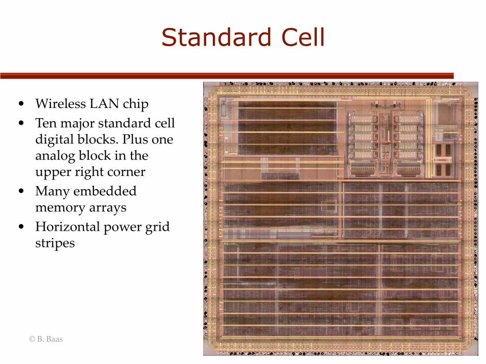
Standard Cell
• Wireless LAN chip
• Ten major standard cell digital blocks. Plus one analog block in the upper right corner
• Many embedded memory arrays
• Horizontal power grid stripes

© B. Baas 20
Combination Standard Cell and Full Custom
• Dense, regular full-custom blocks
• Random logic implemented with standard cells and automatic place and route
[figure from S. Hauck]
© B. Baas 21
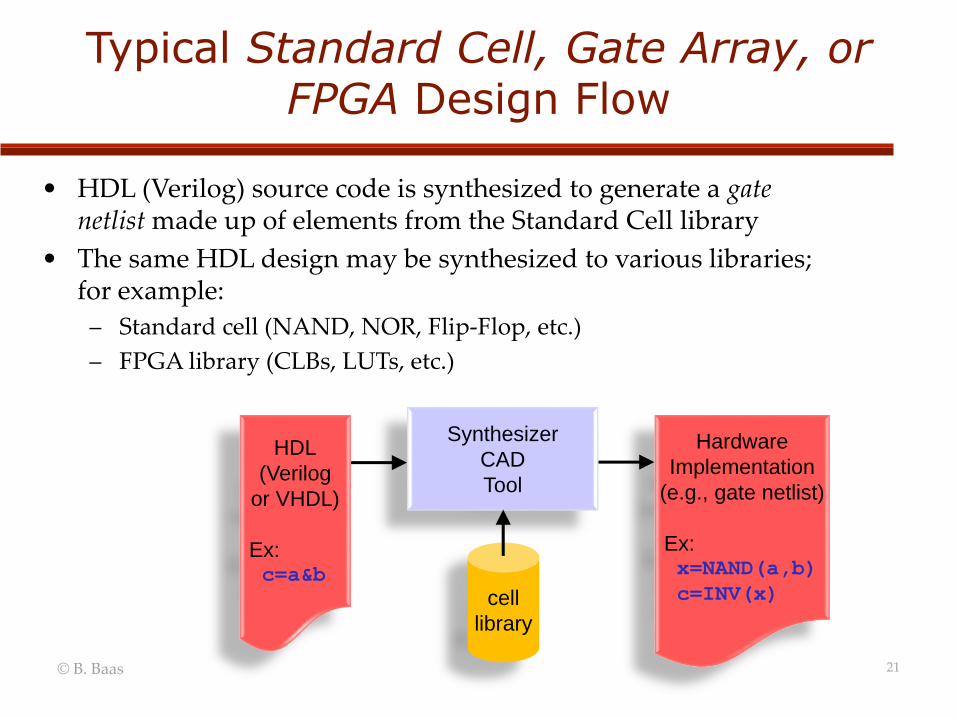
Typical Standard Cell, Gate Array, or FPGA Design Flow
• HDL (Verilog) source code is synthesized to generate a gate netlist made up of elements from the Standard Cell library
• The same HDL design may be synthesized to various libraries; for example:
– Standard cell (NAND, NOR, Flip-Flop, etc.)
– FPGA library (CLBs, LUTs, etc.)
Synthesizer
CAD
Tool
HDL
(Verilog
or VHDL)
Ex:c=a&b
Hardware
Implementation
(e.g., gate netlist)
Ex:x=NAND(a,b)
c=INV(x)cell
library

© B. Baas 22
Simplified diagram of Standard Cell design flow after synthesis
Place &
Route
Design Rule Check (DRC)
Layout vs.Schematic
(LVS) Check
Gate level dynamic and/or static analysis
Gate-level
description
Timing Information
Hardware
Implementation
(e.g., gate netlist)
Ex:x=NAND(a,b)
c=INV(x)
Final Layout (could be
fabricated)

23EEC 116, B. Baas 23
Layout synthesized from Verilog and a Standard Cell library, and then “Placed & Routed”
Source: Digital Integrated Circuits, 2nd ©
module multiplier (
input in1,
input in2,
output out
);
out = in1 * in2;
endmodule

© B. Baas 24
Gate Array
• Polysilicon and diffusion are the same for all designs
• Metal layers customized for particular chips
n-type diffusion
polysilicon
p-type diffusion
PMOS transistor
NMOS transistor

© B. Baas 25
Gate Array
• Polysilicon and diffusion the same for all designs
• 0.125 um example
[figure from LETI]

26EEC 116, B. Baas 26
Gate Array — Sea-of-gates
rows of
cells
routing channel
uncommitted
VDD
GND
polysilicon
metal
possiblecontact
In1 In2 In3 In4
Out
Uncommited
Cell
Committed
Cell
(4-input NOR)
Source: Digital Integrated Circuits, 2nd ©

© B. Baas 27
Field Programmable Gate Array (FPGA)
• Metal layers now programmable with SRAM instead of hardwired during manufacture as with a gate array
• Cells contain general programmable logic and registers
[figure from S. Hauck]

© B. Baas 28
Field Programmable Gate Array (FPGA)
• Chips now “designed” with software
• User pays for up-front chip design costs– All: full-custom, standard cell
– Half: gate array
– Shared: FPGA
• User writes code (e.g., verilog), compiles it, and downloads into the chip
• The flexibility comes at a great cost however; as a very approximate comparison, FPGAs are over 10x slower, less energy efficient, and greater area than an equivalent Standard Cell design

© B. Baas 29
Progrmmable Processor
• Intel 8086
• First released 1978
• 33 mm2
• 3.2 µm
• 4–12 MHz
• 29,000 transistors
© B. Baas 30
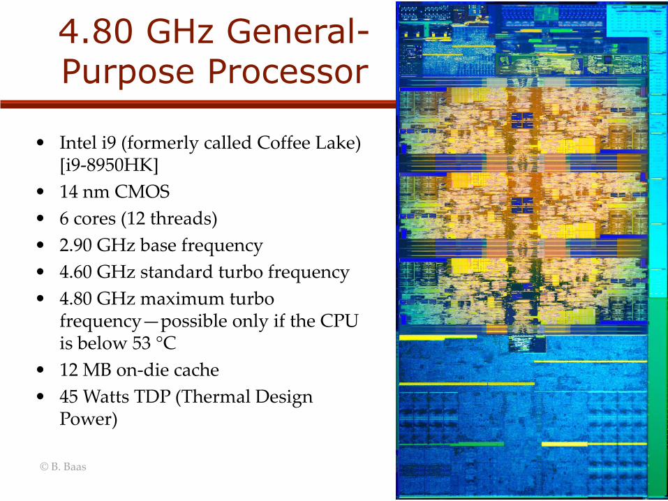
4.80 GHz General-Purpose Processor
• Intel i9 (formerly called Coffee Lake) [i9-8950HK]
• 14 nm CMOS
• 6 cores (12 threads)
• 2.90 GHz base frequency
• 4.60 GHz standard turbo frequency
• 4.80 GHz maximum turbo frequency—possible only if the CPU is below 53 °C
• 12 MB on-die cache
• 45 Watts TDP (Thermal Design Power)

© B. Baas 31
Massive General-Purpose Server Processor
• Itanium Poulson
• 32 nm
• 3.1 Billion Transistors
• 18.2 mm x 29.9 mm = 544 mm2
• 8 multi-threaded cores
• 54 MB total on-die cache
• 170 Watts TDP
• [ISSCC 2011]

© B. Baas 32
Programmable DSP Processor
• TI C64X
• 600 MHz, 0.13 um, 718 mW @ 1.2 V
• 8-way VLIW core
• 2-level memory system
• 64 million transistors
[figure from S. Agarwala]

© B. Baas 33
Massive Special-Purpose Processor
• Nvidia V100
• TSMC 12 nm FinFET
• 21.1 Billion Transistors
• 815 mm2
– Approximately 37.9 mm x 21.5 mm
– At the reticle limit
• 1.45 GHz
• 80 streaming multiprocessors
• 300 Watts TDP
• Memory interface to HBM2 1.75 GHz, 4096-bit bus, 900 GB/s
• [HotChips 2017]

© B. Baas 34
Graphcore

35EEC 116, B. Baas 35
Heterogeneous Programmable Platforms
Xilinx Vertex-II Pro
[Xilinx]
High-speed I/O
Embedded PowerPc
Embedded memories
Hardwired multipliers
FPGA Fabric

36EEC 116, B. Baas 36
Design at a crossroad
System-on-a-Chip
RAM
500 k Gates FPGA
+ 1 Gbit DRAM
Preprocessing
Multi-
Spectral
Imager
mC
system
+2 Gbit
DRAMRecog-
nition
Anal
og
64 SIMD Processor
Array + SRAM
Image Conditioning
100 GOPS
• Often used in embedded applications where cost,performance, and energy are big issues!
• DSP and control
• Mixed-mode
• Combines programmable and application-specific modules
• Software plays crucial role

37EEC 116, B. Baas 37
A System-on-a-Chip ExampleHigh Definition TV Chip
Courtesy: Philips
EEC 116, B. Baas 38
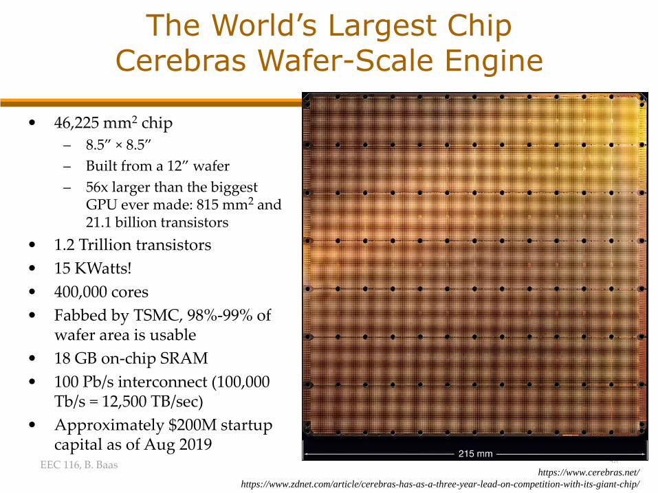
The World’s Largest ChipCerebras Wafer-Scale Engine
• 46,225 mm2 chip
– 8.5” × 8.5”
– Built from a 12” wafer
– 56x larger than the biggest GPU ever made: 815 mm2 and 21.1 billion transistors
• 1.2 Trillion transistors
• 15 KWatts!
• 400,000 cores
• Fabbed by TSMC, 98%-99% of wafer area is usable
• 18 GB on-chip SRAM
• 100 Pb/s interconnect (100,000 Tb/s = 12,500 TB/sec)
• Approximately $200M startup capital as of Aug 2019
https://www.cerebras.net/
https://www.zdnet.com/article/cerebras-has-as-a-three-year-lead-on-competition-with-its-giant-chip/