Embed Size (px)
Citation preview

The art of chemical metal removal has long been practiced by photoengravers in the preparation of printing and engraving plates as well as in the fabrication 01 decorative metalwork and nameplates. However, recently the potential of chemical metal removal has been more fully recognized. As more advanced equipment is developed, and as more knowledge of the process is gained, chemical milling is becoming a specialized metalworking process. For example, with the demands for special hardware in satellites and other space applications steadily increasing, designers find that many of these demands can be satisfied with the aid of chemical milling. This article discusses some of the techniques of the chemical milling process.
CHEMICAL MILLING of SPACE FLIGHT HARDWARE
R. E. Hicks
T he process of chemical milling has been used for decades in the preparation of printing and
engraving plates. But only recently has the potential of chemical milling as a production metalworking process been discovered. A very important aspect of chemical milling, for example, has been its use in the processing of printed circuits. As know-how increases and as more sophisticated equipment becomes available, chemical milling promises to become a standard fabrication process.
R ecent developments in the art of electronic packaging have given rise to many interesting challenges for the packaging engineer. With the state of the art advancing at such a rapid rate, the packager finds himself constantly in need of changing · his packaging techniques. The demand for more electronic data results in doubling and tripling the number of components necessary to produce this information but usually carries the restriction of little or no increase in physical size of equipment. The packager must then abandon some of his present production and fabrication techniques and seek other methods of reaching his objective. Through
March-April 1967
chemical milling, several such demands have been met with the help of Applied Physics Laboratory Space Division system designers. Space vehicles currently being designed and produced at APL contain chassis and circuitry which employ chemical milling techniques.
Inherent advantages of chemical milling or machining over conventional metal working methods include:
1. Initial quantities of newly designed parts can be ready in hours.
2. Since no dies or special jigging are required, . tooling costs are a small fraction of those for conventional methods.
3. Metals with any degree of hardness are worked with ease.
4. Parts are free from burrs and ready for use without additional machining or processing.
5. Design flexibility permits the production of complex shapes which could not readily be mechanically blanked.
6. Production costs and time are less than half of those for conventional methods.
11

The general uses of chemical removal fall into two categories: ( a ) selective metal removal, and (b) non-selective metal removal. Where there is no attempt to control the location of the metal to be removed but rather to remove metal from all surfaces of the part, non-selective metal removal has been applied. Where certain areas of the work are covered with a chemical resistant coating to prevent etching of those areas, the term selective metal removal is used.
The selective metal removal process can be used in several ways-most important of which are weight reduction and functional machining. The first area to be considered is that of weight reduction, otherwise known as structural chemical milling. In most weight-reduction operations, the maintenance of some of the original metal thickness throughou t the milling process is desirable. It is necessary in these cases to protect the areas which must maintain their original form. An example of such a configuration is a skin panel for the outer covering of the satellite. The strength of the panel is maintained at the support points, but unnecessary weight has been removed, resulting in a substantially lighter end product. Figure 1 shows the selective metal removal technique.
SECTION A-A
Fig. I-Example of selective etching for weight reduction while maintaining structural strength.
The second area for consideration is that of functional machining. Functional chemical milling can be considered as selective metal removal for purposes other than weight reduction. Included in this category are printed circuit etching, nameplate etching, and chemical blanking and piercing. The minis tick technique, l developed by the Advanced Packaging Techniques Group, is an excellent exam-
1 C. F. Noyes, "Ministick Packaging-A Further Aid to Satellite Reliability," APL Technical Digest,S, No 3, January-February, 1966, 2-10.
12
pIe of the chemical blanking technique. Figure 2 shows parts fabricated by this method.
While chemical machining techniques are primarily usable on small and medium run quantities of parts and on material thicknesses of less than 0.062 inch, the techniques can also be applied to large quantity runs of hard-to-work metals such as beryllium copper, hard brass, tempered spring steels, kovar, and tempered aluminum. In addition, chemical machining can shape finished products from extremely thin materials without the rough or burred edges produced by shearing or mechanical blanking.
Fig. 2-Example of functional chemical milling in the ministick system.
In the chemical blanking operation with which this article will primarily be concerned, the required sequence of steps coincides with basic photoengraving and printed circuit techniques. However, there is one major exception-a photographic chemical resistant image is put in register onto both sides of the metal blank and both sides of the material are etched simultaneously. The surfaces of the metal are coated with photo resist by spraying, dipping, or whirling. After drying, the metal is slipped between two negatives, like a sandwich, and placed in a photographic printer where both sides are exposed to an ultraviolet light source for a designated period of time. The images are developed, generally by dipping or spraying, allowed to dry, and etched on both sides in double sided, spray etching equipment.
APL Technical Digest
Design and Fabrication Procedures
The development of an electronic package using the chemical milling technique is relatively simple and straightforward and is more economical in time, materials, and manpower than conventional methods of chassis fabrication. Starting with a satisfactory circuit design in the form of a schematic diagram, the following sequence of operations results in a finished chemically milled chassis which will house the electronics for a specific application:
A. Design
1. Development of a complete package layout from schematic diagram.
2. Preparation of artwork for chassis from package la you t.
3. Photo reduction of artwork.
B. Fabrication
1. Preparing base material for photosensitizing.
2. Photosensitizing and reproducing artwork on base material.
3. Chemical milling of chassis details. 4. Cleaning and plating of details. 5. Assembling of chassis details.
Although this article is not in tended to be a comprehensive treatment of manufacturing procedures, the significant steps that affect the above processes are described for the purpose of f amiliarizing the reader with the techniques involved. The chassis used as an example is an interface filter designed for a specific APL satellite.
Design
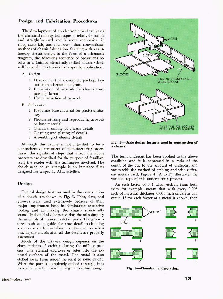
Typical design features used in the construction of a chassis are shown in Fig. 3. Tabs, slots, and
. grooves were used extensively because of their major importance both in eliminating expensive tooling and in making the chassis structurally sound. It should also be noted that the tabs simplify the assembly of numerous detail parts. The grooves serve both as a guide for true detail positioning and as canals for excellent capillary action when brazing the chassis after all the details are properly assembled.
Much of the artwork design depends on the characteristics of etching during the milling process. The etchant engraves or bites into the exposed ~urf aces of the metal. The metal is also etched away from under the resist to some extent. When the part is completely etched through, it is somewhat smaller than the original resistant image.
March-April 1967
/ FORM 90° CORNER USING MILLED GROOVE
TWIST TABS FOR LOCKING DETAIL PARTS IN POSITION
Fig. 3-Basic design features used in construction of a chassis.
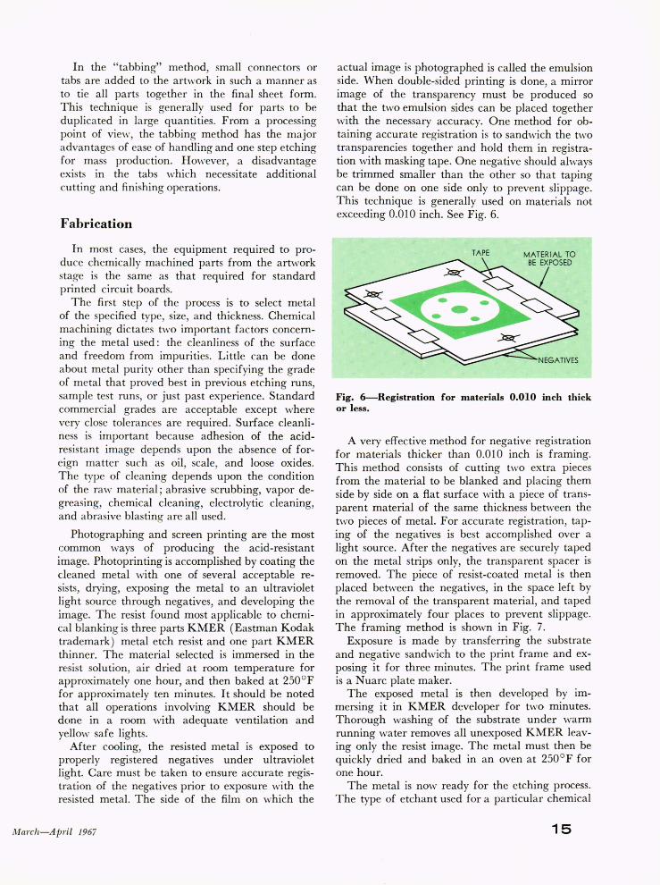
The term undercut has been applied to the above condition and it is expressed in a ratio of the depth of the cut to the amount of undercut and varies with the method of etching and with different metals used. Figure 4 (A to F) illustrates the various steps of this undercutting process.
An etch factor of 3: 1 when etching from both sides, for example, means that with every 0.003 inch of material thickness,O.OOl inch undercut will occur. If the etch factor of a metal is known, then
RESIST ~ ~ D
METAL
c
Fig. 4-Chemical undercutting.
13

it can be used as a means for compensating the artwork. This factor is an important phase of chemical milling; without the proper compensation in the artwork, holding required tolerances on chemically blanked parts becomes almost impossible.
With an etch factor of 3: 1, 0.002 inch undercut will occur on details to be etched from metal that is 0.006 inch thick. At the artwork stage, the outside dimensions of that part then must be increased 0.002 inch all around. The dimensions of cutouts, such as a hole or slot, must be decreased by the same amount.
Because of undercu.tting conditions, there is a minimum size limit for holes, slots, and other piercings. If the sheet stock thickness to be blanked is expressed as t, the following blanking limitations are characteristic:
1. 0.7 t (copper alloys) 2. 1.0 t (steel alloys) 3. 1.4 t (aluminum alloys and stainless steel).
The material used in chemical blanking of the interface filter chassis details was 0.020 inch brass. Thus, the smallest hole that could be chemically pierced in the 0.020 inch brass and still provide a nearly vertical wall would be 0.014 inch.
A basic rule to keep in mind when laying out the artwork is that internal corners will develop radii equal to approximately one half the etched
I I I I I I I I . .
depth. External corners can be held a little sharper. They generally develop radii equal to about one third etched depth.
When large numbers of details are to be chemically milled, it is economically desirable to have multiple images on the same film before photographic reduction. This permits the chemical blanking of several details in the same operation. However, a factor to consider in laying out the artwork for multiple images is the method to be used for retention of the parts during the blanking operation. Two popular methods used for retaining or reclaiming chemically milled parts are known as "dropping out" and "tabbing." While both of these methods are acceptable procedures for retention, each has its advantages and limitations.
The "drop out" method is limited to equipment that is designed to catch or reclaim parts that have been completely blanked out. The artwork for this method is designed in such a manner that an opaque border completely surrounds the part on the subsequent negatives. Etching then occurs on all areas around the part and the part will then drop out onto a screen. The major advantage of the drop out method is that parts are ready for use immediately after resist removal. This condition is advantageous for larger parts; but where several hundred small parts are involved, quite a handling problem can result. Figure 5 shows parts which have been made by the "drop out" method.
,. -. ·t -. ~ - . -. . - - - - .
• . • ..... i -' I ~ ', -' '; ~ 'I ' • ~ . ' • • . .. .. .
Fig. 5-Parts etched using "drop out" method.
14 APL Technical Digest
In the "tabbing" method, small connectors or tabs are added to the artwork in such a manner as to tie all parts together in the final sheet form. This technique is generally used for parts to be duplicated in large quantities. From a processing point of view, the tabbing method has the major advantages of ease of handling and one step etching for mass production. However, a disadvantage exists in the tabs which necessitate additional cutting and finishing operations.
Fabrication
In most cases, the equipment required to produce chemically machined parts from the artwork stage is the same as that required for standard printed circuit boards.
The first step of the process is to select metal of the specified type, size, and thickness. Chemical machining dictates two important factors concerning the metal used: the cleanliness of the surface and freedom from impurities. Little can be done about metal purity other than specifying the grade of metal that proved best in previous etching runs, sample test runs, or just past experience. Standard commercial grades are acceptable except where very close tolerances are required. Surface cleanliness is important because adhesion of the acidresistant image depends upon the absence of foreign matter such as oil, scale, and loose oxides. The type of cleaning depends upon the condition of the raw material; abrasive scrubbing, vapor degreasing, chemical cleaning, electrolytic cleaning, and abrasive blasting are all used.
Photographing and screen printing are the most common ways of producing the acid-resistant image. Photoprinting is accomplished by coating the cleaned metal with one of several acceptable resists, drying, exposing the metal to an ultraviolet light source through negatives, and developing the image. The resist found most applicable to chemical blanking is three parts KMER (Eastman Kodak trademark) metal etch resist and one part KMER thinner. The material selected is immersed in the resist solution, air dried at room temperature for approximately one hour, and then baked at 250 °F for approximately ten minutes. It should be noted that all operations involving KMER should be done in a room with adequate ventilation and yellow safe lights.
After cooling, the resisted metal is exposed to properly registered negatives under ultraviolet light. Care must be taken to ensure accurate registration of the negatives prior to exposure with the resisted metal. The side of the film on which the
March-Apl°il 1967
actual image is photographed is called the emulsion side. When double-sided printing is done, a mirror image of the transparency must be produced so that the two emulsion sides can be placed together with the necessary accuracy. One method for obtaining accurate registration is to sandwich the two transparencies together and hold them in registration with masking tape. One negative should always be trimmed smaller than the other so that taping can be done on one side only to prevent slippage. This technique is generally used on materials not exceeding 0.010 inch. See Fig. 6.
Fig. 6-Registration for materials 0.010 inch thick or less.
A very effective method for negative registration for materials thicker than 0.010 inch is framing. This method consists of cutting two extra pieces from the material to be blanked and placing them side by side on a fiat surface with a piece of transparent material of the same thickness between the two pieces of metal. For accurate registration, taping of the negatives is best accomplished over a light source. After the negatives are securely taped on the metal strips only, the transparent spacer is removed. The piece of resist-coated metal is then placed between the negatives, in the space left by the removal of the transparent material, and taped in approximately four places to prevent slippage. The framing method is shown in Fig. 7.
Exposure is made by transferring the substrate and negative sandwich to the print frame and exposing it for three minutes. The print frame used is a Nuarc plate maker.
The exposed metal is then developed by immersing it in KMER developer for two minutes. Thorough washing of the substrate under warm running water removes all unexposed KMER leaving only the resist image. The metal must then be quickly dried and baked in an oven at 250 ° F for one hour.
The metal is now ready for the etching process. The type of etchant used for a particular chemical
15

milling operation depends upon the type of metal being etched, etching rate desired, and surface finish. The etchant most commonly used for brass, copper, kovar, and steel is ferric chloride. This etchant is most suitable for these metals allowing for a moderate etch time with good edge and surface finishes.
TRANSPARENT MATERIAL USED FOR NEGATIVE ALIGNMENT
Fig. 7-Registration for materials with thicknesses greater than 0.010 inch.
As a matter of interest, the general rule for etching reactions states: the faster an etchant works, the greater will be the chances of degrading the original surface finish. Use of slow etch ants, such as cold alkali and cold or diluted acid, will result in a surface finish nearly equivalent to the original finish. Where increased speed is of prime importance, extremely concentrated acids may be used on metals such as aluminum and magnesium to achieve etching rates in excess of 0.010 inch per minute. Of course, the price of such speed is poor surface finish and edges.
After the parts have been blanked, the resist must then be removed. This step is accomplished simply by rubbing the surface with an acid brush and resist remover. A thorough washing in running water and subsequent drying completes the process.
In the design stage of the filter chassis discussed throughout this article, it was decided that the chassis be of brass and that all joints and seams be soldered. For best soldering results, all details are given a 0.0002 / 0.0004 inch tin plate before assembly. All parts are assembled and locked into place by inserting the extended tabs through their designated slots and twisted approximately 45°. End posts hold the corners of the chassis securely in place and fasten the filter into the satellite. The studs, used for holding the covers, are hand pressed into place.
16
After the chassis is assembled it is placed on a preheated hot plate and heated for approximately one hour at 500°F. At this point, the chassis is fluxed. With the aid of an acetylene torch, a small amount of stainless solder is applied to corners and joints. The heat of the torch also causes the tin to liquefy and, by capillary action, flow into the chemically milled grooves around the walls and joints. The chassis is then cooled and cleaned.
The tabs used for holding the chassis during the above process are then cut off flush with the surface. The only step remaining is a final tin plating. Figure 8 shows the completed interface filter.
Fig. 8-Interface filter.
Summary
The chemical milling process has been shown to have both advantages and limitations. The many advantages include the fact that the setting up and tooling costs are extremely low, since artwork and negatives are the only tooling required once the initial camera and etching setups have been installed. Newly designed parts can be produced with remarkable speed. Revisions to such parts cost little because only the artwork needs to be altered. Extremely thin materials can be easily worked without special machinery, and the accuracy increases as the metal thickness decreases. Metal hardness poses no significant problem. The physical properties of temper and stress are not affected. For example, a brittle metal, such as silicon electrical steel, which often fractures during conventional blanking is chemically blanked with ease.
Limitations to the chemical milling process include: necessity of relatively high operator skill; etchant vapors are very corrosive and must be isolated from other equipment; good photographic facilities are not always available; and the maximum metal thickness is about 7i 6 inch.
The advantages of chemical milling far outweigh the limitations. With its unlimited design flexibility, the chemical milling process will aid in the solution of many complex hardware problems.
.\PL Technical Digest