Embed Size (px)
Citation preview

CHARGE TRANSPORT IN CONJUGATED POLYMERS
Yohai Roichman

CHARGE TRANSPORT IN CONJUGATED POLYMERS
Research Thesis
Submitted in Partial Fulfillment of Requirements for the Degree of
Doctor of Philosophy
Yohai Roichman
Submitted to the Senate of the Technion – Israel Institute of Technology
Elul 5764 HAIFA August 2004


In memory of my father, Eliahu Roichman.
For mother,
Yael, Elad and Lilach


The research thesis was done under the supervision of Prof. Nir Tessler in electrical engineering faculty in the Technion. My thanks are due firstly to Nir Tessler, for suggesting this problem. I wish to express my sincere appreciation for the original thinking Nir shared with me and for the extensive support and guidance during this work. This work was greatly facilitated by the meetings and the valuable correspondence with Harvey Scher, Heinz Bassler, and Vladimir Arkhipov. I thank Yossi Rosenwaks for the scientific collaboration, and Oren Tal for spending long hours in and near the Kelvin force probe microscope room, that were the result of this collaboration. I thank Yevgeny Preezant for teaching me numerical analysis and for rechecking me. I thank Oded Katz for the "afternoon collaboration" that resulted on new methods to analyze FETs and coffee over-dose. Special thanks for Vlad Medevdev, Yair Gannot and Andrea Peer, that each in his turn contributed for the design and fabrication of the polymer field effect transistors, and for amusements at the long hours in the lab. Thanks for Daniel Lubzans, Yaakov Schneider and all of the microelectronic research center staff, Otilia, Mark, Ron, Giora, Pnina… for all of the help that is always was served with a smile. Dear mother, thank you for the love and for teaching me curiosity, Thanks for my dearest sister and brothers Tirtsa, Hanani and Yuval, for helping me during happy and sad days. Finally my love and appreciation are for Yael, Elad and Lilach that help go through this "long distance run" with a smile on my face (besides, it is always nice to have a physicist in the house to consult with…). The financial support of Israel ministry of science in this project is gratefully acknowledged. The generous financial help of the Technion, Eshkol foundation and the Israel science foundation is gratefully acknowledged.


Contents
Contents
Abstract ..................................................................................................................1
List of Symbols ......................................................................................................3 Preview...................................................................................................................7 1. Literature Survey.............................................................................9
1.1 On Transport Definitions............................................................................9 1.1.1 Master equation for transport on a discrete grid..................................9 1.1.2 Transport Green function - mobility and diffusion ...........................10 1.1.3 Anomalous charge transport..............................................................12
1.2 On Conjugated Polymers as Amorphous Semiconductors....................15 1.2.1 The role of disorder ...........................................................................15 1.2.2 Electronic and physical properties of conjugated polymers and related
materials...........................................................................................17 Charge carriers in conjugated polymers – the polarons ............18 The density of states, and other properties of the excited states.20
1.2.3 Charge carrier hopping mechanism..................................................24 1.3 Charge Transport in Conjugated Polymers - Models and Experimental
Evidences.....................................................................................28 1.3.1 Experimental observations of transport properties in diluted
materials...........................................................................................28 1.3.2 Variable range hopping model .........................................................30 1.3.3 Dispersive transport and the continuous time random walk theory 32 1.3.4 Non-linearity of charge transport properties with charge
concentration ...................................................................................33 The Organic Field Effect Transistor (OFET) .............................35
2. The Transport Calculation .....................................................39
2.1 Introduction.................................................................................39 2.2 The Transport Model....................................................................40 2.3 On Near Equilibrium Conditions – Degeneracy and Einstein
Relation .....................................................................................42 2.3.1 The distribution function .................................................................42 2.3.2 Are conjugated polymers non-degenerate? .....................................44 2.3.3 The generalized Einstein relation ....................................................46
2.4 Mobility at Near Equilibrium Conditions – the Mean Medium Approximation .............................................................................52
2.4.1 Mobility calculation for a general form of density of states............52 2.4.2 Mobility calculation for a gaussian density of states.......................55
Hopping mobility dependence upon charge concentration and electric field ................................................................................56 Temperature dependence of the hopping mobility......................58

Contents
Mobility dependence on the density of states..............................61 Hopping rate from a given initial site.........................................65
2.5 Mobility in Calculation for Realistic Spatial Site Distribution - The Effect of Morphology ...................................................................67
2.5.1 Inhomogeneous Solution of the Mean Medium Approximation.....67 2.5.2 The discrete master equation direct solution ...................................71
2.6 Summary and Discussion .............................................................76
3. Experiments in Polymer Field Effect Transistors..................... 79 3.1 Introduction.................................................................................79 3.2 Experimental Methods..................................................................80
3.2.1 Polymer Field Effect Transistor Process .........................................80 3.2.2 Electrical Characteristics – DC and Time Resolved Measurements81 3.2.3 Atomic Force Microscope in Kelvin Probe mode ...........................82
Results and Discussion............................................................................84 3.3 Structural Parasitic Effects in Polymer FET .................................84 3.4 Channel charge build-up ..............................................................89 3.5 Mobility Extraction from Transfer Characteristics.........................95
3.5.1 Mobility extraction methods in field effect transistors....................95 3.5.2 Mobility extraction polynomial expansion formalism ....................96 3.5.3 Determination of the threshold voltage ...........................................99
3.6 Charge transport characteristics of MEH-PPV ............................ 102 3.6.1 Mobility dependence on charge concentration and charge carrier
DOS in MEH-PPV.........................................................................102 3.6.2 The effect of morphology and the intrinsic activation energy .........107
4. Overview ............................................................................. 109
4.1 Summary and discussion ............................................................ 109 4.2 Outlook...................................................................................... 113
Appendices ............................................................................. 115 Appendix A: Approximations for Generalized Einstein Relation in a Gaussian Density of States 115 Appendix B: Mobility calculation by the homogenous mean medium approximation 119
B.1 Reducing the MMA homogenous current equation from 3D into 1D 119 B.2 Low field linearization of the Miller Abrahams MMA mobility 120
Appendix C: Mobility calculation by the inhomogeneous mean medium approximation 123
C.1. Reducing the MMA inhomogeneous current equation from 3D into 1D 123 C.2. MMA calculation of the Miller-Abrahams mobility of step radial correlation function 126
Appendix D: Matlab code for Mobility and Einstein relation MMA calculation 129 Appendix E: Process procedure for bottom contact PFET substrates 133 Appendix F: Accumulation layer width 135 Appendix G: The measured polymer field effect transistors properties 141
Bibliography ............................................................................143

Contents

List of Figures
List of Figures
Figure 1: Continuous time random walk (CTRW) (b), versus Markovian random walk (a). The size of the circles represents the time delay at each point. (Follows Metzler et. al., Ref. 14)...................................................................................................................14
Figure 2: The Transport Green function for: Markovian random walk (a) versus Continuous time random walk (CTRW) with β=0.5 (b). (From Scher et. al., Ref. 4).14
Figure 3: Three possible types of density of states in an amorphous material: a) Free states band with a localized band at the forbidden energy gap (trap band), b) free states band with a localized tail, b) fully localized band. ............................................16
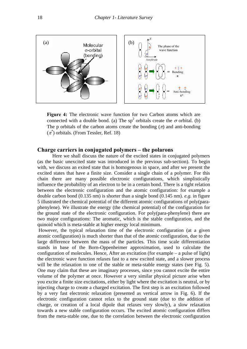
Figure 4: The electronic wave function for two Carbon atoms which are connected with a double bond. (a) The sp2 orbitals create the σ orbital. (b) The p orbitals of the carbon atoms create the bonding (π) and anti-bonding (π*) orbitals. (From Tessler, Ref. 18) ........................................................................................................................18
Figure 5: The energy level versus configuration of poly(para-phenylene). The stable aromatic and the meta-stable quinoid configurations are illustrated. (From Tessler, Ref. 18) ........................................................................................................................19
Figure 6: Excitation and atomic relaxation as described by Frank Condon principle. 20
Figure 7: A schematic illustration of the different excited states in poly(para-phenylene) (from top to bottom): The major stable configurations, a positive polaron, an exciton, a positive bipolaron. ......................................................20
Figure 8: Histograms of the injection thresholds for charge-carrier injection into a thin film of Me-LPPP deposited on an Au(111) substrate, indicating the DOS shape. (a) region without and (b) region with aggregates. (From Alvarado et. al Ref. 58). ........23
Figure 9: The free energy curve versus one of the configuration coordinates (e.g. the bond length in one of the molecules), for the reactants (R) and the products (P). (From Marcus, Ref. 63) ..........................................................................................................26
Figure 10: A schematic description of the time of flight (TOF) experiment (a) and the current-time (I-t) typical curve (b). ..............................................................................29
Figure 11: Typical results of mobility dependence on temperature and electrical field as obtained from TOF experiments (From Pfister et. al. Ref. 78 (a) and Kageyama et. al. Ref. 76 (b)) ..............................................................................................................29
Figure 12: The effect of energy correlation. The mobility versus the square root of the electric field, as calculated by a Monte Carlo simulation, with and without correlation between sites energy. (From Gartstein and Conwell, Ref. 87) ...................................31
Figure 13: Temporary distribution of the charge carriers in GDM model as calculated from Monte Carlo simulation. (From Bassler, Ref. 8).................................................31

List of Figures
Figure 14: The typical "finger prints" of dispersive transport: long current decay in the I-t curve (a). Scaling low of different thickness samples curves (b), which can be divided in log-log scale into two sections with a different slopes. (From Scher and Montroll, Ref. 3 ). ........................................................................................................32
Figure 15: The effect of molecular doping on charge mobility in poly(3-hexylthiophene), experimental (From Jiang et. al. Ref. 93) and calculation (From Arkhipov et. al. Ref. 94) ...................................................................................33
Figure 16: The change in the transport properties in the TOF experiment with the illumination optical density. (From Bos and Burland, Ref. 98)...................................34
Figure 17: Organic field effect transistor (OFET) schematic typical structures: a) bottom contacts, b) top contacts...................................................................................35
Figure 18: The mobility dependence uppon the gate bias as demonstrated by Brown et.al. [1997]103 (a), Horowitz et. al. [1998]108 (b), Tanase et. al. [2003]106 (c) from the FET transconductance, and by Burgi et. al. [2002]109 by Kelvin probe atomic force microscopy (KPFM) of an OFET. ...............................................................................37
Figure 19: Logarithm of mobility against the electric field with different carrier densities for a system with randomly distributed traps. (From Yu et. al. [2001]74) ....37
Figure 20: A schematic presentation of the electronic sites in conjugated polymers as distributed in space (a) and in energy along a cross-section (b). .................................40
Figure 21: A schematic presentation of a realistic electronic state distribution in amorphous semiconductors. The electronic sites (index i) contain discrete electronic states (index j) manifold as a result of the quantum confinement. ..............................43
Figure 22: Schematic description (a) and an accurate calculation (b) of charge carrier distribution in a gaussian DOS at different chemical potentials..................................46
Figure 23: The generalized Einstein relation (GER) versus the chemical potential....49
Figure 24: The inverse generalized Einstein relation (GER) versus the chemical potential (a) and the normalized charge concentration (b) for different gaussian DOS widths. ..........................................................................................................................49
Figure 25: The generalized Einstein relation (GER) versus the temperature at constant charge concentrations...................................................................................................50
Figure 26: Simulation results of TOF photo-current response for two Gaussian DOS.......................................................................................................................................51
Figure 27: A schematic energy-space 2D projection of a discrete random walk on a lattice (a) and the equivalent mean medium approximation (b). .................................53
Figure 28: The mobility versus the chemical potential (for DOS width 5σ = ). ........56
Figure 29: The mobility versus the electrical field for different charge concentration (for DOS width 5σ = ).. ..............................................................................................57
Figure 30: The mobility versus the electric field and for different charge concentration (a) and the mobility versus the chemical potential (charge concentration) for different electric field (b)............................................................................................................58
Figure 31: Miller-Abrahams hopping current (a) and mobility (b) versus the applied field at different temperatures ......................................................................................59

List of Figures
Figure 32: Miller-Abrahams mobility dependence upon the inverse temperature for a given charge concentration and different electric fields (a). The cross over temperature (T0) as determined by the cross section of mobility versus field curves at different charge concentration (b)................................................................................59
Figure 33: The activation energy of the mobility versus the electrical field for different charge concentration (for Miller Abrahams transfer between sites). ............60
Figure 34: The mobility versus the chemical potential(b), and versus the charge carrier concentration (c) for different DOS shapes (a)............................................................62
Figure 35: The exponential factor as a function of the Gaussian width at T=300k.....63
Figure 36: The calculated mobility as a function of charge density at T=300k.. ........64
Figure 37: The dependence of the power law coefficient (κ) on the DOS width σ/kT for the low electric field regime at T=300k. ................................................................65
Figure 38: The hopping probability from a given site i to a final energy jε at different applied fields (a-d). The applied field and the current from site i is marked on the effective mobility for charge carrier at energy iε curve (e). .......................................66
Figure 39: A schematic description of realistic site distribution and the equivalent radial correlation function............................................................................................67
Figure 40: Hard sphere model of conjugated polymer: the conjugated segments are equivalent to the metallic core, and the side chains are equivalent to the insulating shell.. ............................................................................................................................69
Figure 41: The calculated low field mobility versus the minimum width insulator width- BS (a), and the typical dimension of the system - 0S SL B R+ + (b).. ...............70
Figure 42: Full calculation of the mobility in a full range of electric field and charge concentration for different morphological parameters. ...............................................70
Figure 43: A comparison between the MMA calculation (described above) of the mobility and the accurate calculation of the mobility in 1D system by Derrida's formula82. .....................................................................................................................71
Figure 44: The number of nearest neighbors in different systems: 1D system – 2 n.n. (a), A schematic description (2D plot) of close random packed 3D system – 5-8 n.n.(b), mean medium approximation ∞ n.n. (c). .......................................................72
Figure 45: A 3D plot of (part of) the matrix of the close random packed spheres (a), and the equivalent calculated radial correlation function (b) used for the Master equation direct solution................................................................................................73
Figure 46: The calculated mobility from the Master equation solution of two representative runs, and the result of the MMA calculation at different chemical potential values. ...........................................................................................................74
Figure 47: The occupation probability factor of the sites in 1D system. While the zero field occupation probability follows Boltzmann distribution (a), the occupation probability deviates significantly from Boltzmann distribution even at moderate fields (b). ......................................................................................................................75
Figure 48: The occupation probability factor of the sites in 3D system.. ....................75

List of Figures
Figure 49: A schematic cross-section of polymer field effect transistors PFET, bottom contacts (BOC) and top contacts (TOC) structure. ......................................................80
Figure 50: Time resolved measurement setup for the short time scale........................82
Figure 51: Three designs of bottom contact structure: Simple comb design(a). The polyimide-field oxide (b). The closed topology design (c)..........................................85
Figure 52: Measured drain current for BOC with polyimide field oxide (a) and TOC (b) structures. ...............................................................................................................85
Figure 53: Measured drain current as a function of time after applying a gate bias for top contact (TOC) and bottom contact (BOC) structures. ...........................................85
Figure 54: An equivalent circuit of TOC transistor with all of the parasitic resistances and capacitances...........................................................................................................87
Figure 55: An equivalent circuit of BOC with a closed topology transistor with all of the parasitic resistances and capacitances....................................................................87
Figure 56: 2D calculation (Poisson + continuity equations) results of TOC transistor, at different times after gate opening. ...........................................................................88
Figure 57: (a) Calculated 2D potential distribution for the TOC structure. The transistor active region has reached its steady state. (b) Schematic description of the potential distribution between the contacts for varying drain voltage. ........................88
Figure 58: The influence of electrode metal/polymer diodes (contact resistance). A schematic description (a), and a real MEH-PPV transistor with Au electrodes measurements (b). ........................................................................................................89
Figure 59: Conductance (a) and transconductance (b) characteristics of PFET with a negligible contact resistance. .......................................................................................89
Figure 60: Measured source and drain currents of PFET after switching the gate voltage from 0 V to -8 V..............................................................................................90
Figure 61: Transmission line method (TLM) Calculated surface charge in the FET channel at different elapsed times after operating gate bias for: (a) low drain voltage, and (b) high gate voltage..............................................................................................92
Figure 62: Experimental and transmission line simulation results of PFET charging current for different gate voltages................................................................................93
Figure 63: Typical mobility dependence on charge concentration in conjugated polymers based FETs. The mobility is extracted by the conventional transconductance method (UT), the current equation method (UMC), and by the suggested polynomial expansion method (PE). ...............................................................................................98
Figure 64: Three calculated transconductance current characteristics of PFETs with constant threshold voltage: constant mobility (blue, solid), concentration dependent mobility, and constant mobility with a low doped bulk.............................................100
Figure 65: Kelvin probe and topography force microscopy scan results (a) of 9 [ ]mµ channel PFET operated at VDS=-4 [V] and VG between -6 and -1 [V]. ........101
Figure 66: Transconductance measurement results of "normal" MEH-PPV FET (a) and mobility extraction results by three methods. .....................................................103

List of Tables
Figure 67: Transconductance curves of MEH-PPV PFET with low threshold shift (a). The threshold voltage extracted from high current is lower than the switch-on bias. The mobility dependence on the gate bias (b) was extracted by PE and UMC methods were the threshold voltage was determined by the condition that the mobility extracted from the different VDS curves should converge. ........................................104
Figure 68: (a) Current characteristics of the MEH-PPV PFET that was measured by the KPFM. (b) The PE calculated mobility from different VDS curves. ....................106
Figure 69: (a) The charge density as a function of gate voltage (left axis). (b) The mobility as a function of charge density. 117. .............................................................106
Figure 70: Transfer characteristics of PFETs made of MEH-PPV in three molecular weights. ......................................................................................................................108
Figure 71: Transfer characteristics of PFETs made of MEH-PPV (MW=2.8 M) (a), and the Arrhenius plot of two MEH-PPV based transistors at different MW (b). The activation energy in both measurements is identical, at very high accuracy. ............108
Figure 72: A(σ ) and B(σ ) coefficients dependence on the normalized standard deviation σ , as extracted from a linear fitting. .........................................................116
Figure 73: The ( , ,z )ϕijR coordination system. Z is in the direction of the field ...119
Figure 74: The ( ),j zε plane. .....................................................................................120
Figure 75: Two adjacent conjugated sites in the metallic core approximation..........124
Figure 76: The radial correlation function and the equivalent transformed correlation function (TCF) for three examples of correlation functions: a step function, δ function and an example for a general expansion of general form of a correlation function. .....................................................................................................................125
Figure 77. Simulated charge density (2D simulation) and potential at the middle of the channel for p-channel transistor and a bias of VDS=(VGS-VT)=-1..............................135
Figure 78. Calculated charge density profile for two electric fields at the insulator .137
List of Tables
Table 1: The relation between observations and their possible origins.....................112 Table 2: A(σ ) and B(σ ) coefficients dependence on the normalized standard
deviation σ , as extracted from a linear fitting………………………......116 Table 3: coefficients for equation (5.1.5) which is used to calculate the generalized
Einstein relation (GER)................................................................................117 Table 4: The parameters used for Fig. 78..................................................................137 Table 5: Technical data of the measured PFETs....................................................... 143

Abstract 1
Abstract
Conjugated polymers, and organic semiconductors in general are a family of electronic materials that are based on π -conjugated carbon atoms. The electro-optical properties of this family of materials raised a significant scientific and commercial interest in the last three decades. Although we witnessed in the recent years the appearance of new commercial applications that are based on these materials, the basic scientific understanding of the fundamental electro-optical processes in organic semiconductors is far from a full understanding. In particular, in this research we examined charge transport properties in conjugated polymers and other amorphous materials. The main goal of this research is to examine theoretically and experimentally the dependence of charge transport properties on the charge concentration, namely the non-linearity of charge transport properties.
The examination of the charge transport properties that is presented here is in the framework of non coherent variable range charge transfer (e.g. variable range hopping). In previously published papers two different models were developed in order to explain charge diluted linear systems and non-linearity of mobility on charge concentration at low fields. Our main theoretical goal was to develop a unified model and calculation method that will enable to explain low concentration and high concentration transport observed properties. In the first part of the thesis we present a calculation method based on a mean medium approximation that enable to calculate transport properties near equilibrium conditions. By this approach we demonstrated that the mobility and Einstein relation (diffusion coefficient to mobility ratio) are highly dependent on charge concentration. We demonstrated that the variations in the properties between high-field low concentration devices (as light emitting diodes) and high concentration low-field high concentration devices (as field effect transistors) can be explained. We developed new methods to determine the intrinsic activation energy (the polaronic binding energy) and the density of states from mobility measurements. And finally, examine the validity of the near equilibrium assumption by removing it and calculating the transport properties directly from the Master equation.
The non-linearity of the charge transport was examined in conjugated polymers field effect transistors. For this goal we developed a polymer field effect transistor design that minimizes parasitic phenomena (mainly, parasitic currents and threshold shift). We closely examined the channel charge build-up process and demonstrated that in most of the applied biases range it is governed by the maximum mobility value. We examined the mobility dependence on charge concentration mainly by close examination of the transfer characteristics of the polymer field effect transistors, and by Kelvin force probe microscopy as well. We developed new analysis methods to determine accurately the threshold voltage (from Kelvin probe force microscopy and from time resolved characteristics of the transistors), and the exact mobility dependence on charge concentration (the polynomial expansion method to analyze transfer characteristics).
We examined closely field effect transistors that were fabricated from one material system (MEH-PPV in numerous molecular weights) by the methods described above. We found that the mobility was found to increase significantly (by

2 Abstract
more than 100) with increasing charge concentration. In a significant portion of the polymer field effect transistor we could identify three conductance region: a) low concentration region, that we associate with "out of the mean medium approximation" behavior, b) intermediate highly concentration dependent mobility region, c) high concentration, constant mobility region. We found that in MEH-PPV there is an intrinsic activation energy that is not related to the molecular weight , which is equivalent to a polaronic binding energy of
215 20 [meV]±410 20 [meV]± (assuming the
polaronic model is valid). Finally, we found a close relation between the morphology (controlled by the molecular weight) and the mobility. Most of our experimental results (except the very low concentration dependence of mobility) stand in a good agreement with the predictions derived from mean medium approximation variable range hopping in inhomogeneous systems.

List of Symbols 3
List of Symbols
Symbol Meaning
c Mobility exponential pre-factor ( ) (, ,f f )ε η ε Distribution function
( )g ε Density of states
ig Degeneracy factor j Current k Boltzmann coefficient p Charge concentration q Charge carrier charge, electron charge r Sphere radii t Time ton Switch-on time tox Oxide width w(t) Waiting time distribution x Position vector z Distance along the charge flow direction BS Minimum insulator width D Diffusion coefficient EF Quasi chemical potential (not Fermi level) EM Mobility edge EC Conductance band edge EV Valence band edge EA Intrinsic activation energy EP Polaronic binding energy G(x,t) Transport Green function J Current Lch Channel length LS Core diameter Pi Probability of site i to be occupied P Probability vector Q Total charge in the channel Rij State to state spatial vector Rij State to state distance
Z Transformed correlation function S Degeneracy factor T Temperature T0 Mobility slope inversion temperature Tg Glass transition temperature VT Threshold voltage VT,ext Extrapolated threshold voltage

4 List of Symbols
Symbol Meaning
Ton Switch-on voltage Wch Channel width Z Distribution function BOC Bottom contact CV Capacitance voltage CTRW Continuous time random walk DOS Density of states ER Einstein relation FET Field effect transistor GDM Gaussian density of state model GER General Einstein relation HOMO Highest occupied molecular orbital KPFM Kelvin probe force microscopy LED Light emitting diode LUMO Lowest unoccupied molecular orbital MMA Mean medium approximation n.n. Nearest neighbors PE Polynomial expansion (method) PFET Polymer field effect transistor PPA Percolation path approximation TFT Thin film transistor TOC Top contact TOF Time of flight UMC Uniform mobility current (method) UT Uniform mobility transconductance (method) VRH Variable range hopping WTD Waiting time distribution (function)
,α κ Mobility concentration exponent β Inverse temperature (1/ ), dispersive transport exponent kTε Energy, dielectric constant ε Normalized energy
0ε Center density of state energy, permittivity of free space
oxε Permittivity of oxide
iε Energy of state i γ Inverse localization radii η Chemical potential/quasi chemical potential, normalized GER η Normalized chemical potential/ quasi chemical potential σ Density of state width, conductivity, carbon conjugated orbital σ Normalized density of states µ Mobility
0µ Mobility pre-exponential factor
( ) ( ), Rρ ρijR Spatial/radial correlation function ξ Normalized Einstein relation π Carbon conjugated orbital
( )tψ Waiting time distribution function

List of Symbols 5
Symbol Meaning
ijυ Transfer rate
0υ Envelope function of transfer rate Ω Transfer rate matrix ∆ Mobility zero field activation energy Σ Off diagonal disorder

6
List of Symbols

Preview 7
Preview
In 1977 high conductance in doped polyacetylene was found1. Since this discovery the field of conjugated polymers (conductors and semiconductors) received a significant scientific as well as commercial intention, mainly due to the discovery of highly efficient electroluminescence in this family of polymers, and the utilization of light emitting diodes as well as other devices based on these materials2 (in particular, field effect transistors and photovoltaic cells). The new discoveries in this field and the vast advance in the conjugated polymers quality and variety of materials, resulted in emerge of new commercial applications, for instance flat displays, and flexible circuits (currently developed, and some commercially available). Although material technology advanced significantly at the last two decades, a fundamental understanding of the basic electro-optical processes in these materials is still under debate, and extensive research. In this research we focused on one of the basic properties of the amorphous semiconductors, namely on charge transport. Most of the research on this subject concentrated at the last three decades on the examination of charge diluted systems that can be described as linear system. One of the primary reasons to concentrate on this region was the fascinating finding of a new mode of transport that deviates from the "normal" Markovian transport – namely, anomalous or dispersive transport (namely, non-Gaussian transport)3,4. An exception to this approach was the finding that charge transport is strongly dependent on charge concentration in organic/ conjugated polymers field effect transistors5,6. However, these experiments were described in terms that were different from the common models used for low concentration devices (e.g. exponential DOS7 rather than gaussian DOS8). For this reason, the major goal of this research was to find a unified model and calculation method that will enable to describe a wide variety of experiments/ devices by a single model, and to examine some of the predictions of this calculation in a single device – polymer field effect transistor. In the following chapters we will describe previously developed approaches and findings related to charge transport in amorphous organic semiconductors, the theoretical calculation methods we developed, and the experimental investigation of polymer field effect transistors, by this order.

8

Chapter 1- Literature Survey
9
Chapter 1
Literature Survey
In this chapter the conjugated polymers as semiconductors are reviewed. We concentrate on the electrical properties of the conjugated polymers, particularly on the charge carrier transport. At first we present the mathematical and phenomenological physical concepts used to describe transport, particularly convection. On the second section we describe the "building blocks" of the conjugated polymers as semiconductors, namely the structure, charge carriers properties, density of states characteristics etc. The existing models that describe the charge transport in organic disordered semiconductors are presented in the third section, with a special respect to the variable range hopping model. One of the features of this model is that at short enough time scale the transport deviates from the normal Gaussian (Markovian) transport. For this reason we present one of the principle theories that describe far from equilibrium transport (anomalous transport), namely the continuous time random walk (CTRW) theory. We review experimental evidences that support these theoretical approaches, with special emphasis on the role of the charge concentration in the charge transport, namely, the non-linearity of the transport phenomenon. These results, especially the results in the polymeric field effect transistors (π-FETs), will be reviewed in details as the motivation to examine the role of charge concentration in this research was originated from them.
1.1 On Transport Definitions This section is a brief description of the fundamental mathematical and
physical concepts that describes transport phenomenon. Most of this section follows Chaikin's and Lubensky's book9, and serves as a short "dictionary" that defines the terminology that is used in the rest of the text. We focus on diffusion with an applied field on a discrete lattice, as this is the basis for the transport model we use in the following text.
1.1.1 Master equation for transport on a discrete grid In this section the transport equations on a discrete grid are presented. The
conservation law for the total number of particles (charge carriers) is given by the continuity equation:
( ),p tt
0∂+ ∇ ⋅ =
∂j x (1.1.1)
where p and j are the charge carrier concentration and the current, respectively. A discrete form of the continuity equation, namely the Master equation

10 Chapter 1- Literature Survey
is given below. We assume that the particles move on a given lattice (or a grid) that contains discrete sites.
( ) ( ) ( ) ( ) ( ) ( ) ( )''
,, 1 , 1 ', ,ji ij
j j
P i tP j t P i t t P j t t P i t
tυ υ
∂ ⎛ ⎞= − − −⎡ ⎤ ⎡ ⎤⎜ ⎟⎣ ⎦ ⎣ ⎦∂ ⎝ ⎠
∑ ∑ (1.1.2)
where P(i,t) is the probability of site i to be occupied at time t, and the transition rate between an occupied site i to an unoccupied site j is given by the factor ( )ij tυ . The
factor is the result of an exclusion law( )1 ,P i t−⎡⎣ ⎤⎦* of the particles, explicitly double
occupation of a site is forbidden. If a system is diluted the exclusion factor can be approximated to 1, and the particle motion is un-correlated. The Master equation becomes linear with the occupation probability:
( ) ( ) ( ) ( ) ( )'
'
,,ji ij
j j
P i tt P j t t P i t
tυ υ
∂ ⎛ ⎞= −⎜ ⎟∂ ⎝ ⎠
∑ ∑ , (1.1.3)
The linear Master equation can be written in an algebraic notation as:
( ) ( ) ( )t t t t+ ∆ =P Ω P (1.1.4)
where P is the probability (concentration) vector and Ω is the rate matrix:
( )( )
( ), 1ij
ijj i
t t i ji j t t i j
υυ
≠
⎧ ∆ ∈⎪= ⎨≠
− ∆ ∈ =⎪⎩
∑Ω (1.1.5)
1.1.2 Transport Green function - mobility and diffusion In this section we present the properties of a linear continuity equation which
is analog to the linear Master equation on a dense grid. In this occasion there is a linear response function - the Green function, that determines the probability for a particle to be at time t and location x, given that at 't t= it was at ' (x is the location vector). The Green function allows us to determine the density at time t given the density at an earlier time density t' by
=x x
( ) ( ) ( ), ' ', ' 'p t d G t t p tℜ
= − −∫x x x x x , '
)
(1.1.6)
where is the transport Green function satisfying the boundary condition: ( ,G tx
( ) ( ), t 'G δ= −x x x (1.1.7)
For times t>0, ( ),G tx satisfies the same equation as ( ),p tx ; explicitly the continuity equation (equation (1.1.1)), or on a discrete grid the linear Master equation (Eq. (1.1.3)). The Green function cannot be determined without additional information as the implicit Master equation. For example, at conditions far from equilibrium the Green function may be very non-symmetrical (e.g. section 1.1.3). Now, consider a
* The exclusion law may result from Pauli exclusion principle, or from other physical origin (e.g. Coulomb repulsion between particle, as will be demonstrated below).

Chapter 1- Literature Survey 11
physical system that operates with an applied external potential, at near equilibrium conditions (as will be defined at chapter 1.2.2). A common assumption made for such a system is that there are only two components of the total current*: 1) A diffusion current, as described by Fick's law:
( ) ( ),diff t D p= − ∇ , tj x x (1.1.8)
where D is the diffusion constant 2) A drift current, which resembles a linear relation between the potential gradient and the average particle velocity.
( ) ( ) ( ), ,drift t q p t tµ η= ∇ ,j x x x (1.1.9)
where q is the charge of a single particle, ( ), tη x is the local quasi chemical potential and µ is the mobility.
The mobility and the diffusion coefficient do not have to be constant with the potential gradient (the local electrical field) in the general case. Though, if we examine a short enough range or fix the electrical field to a constant value, µ and D will be constant with respect to time and space. These conditions define the normal transport, or the Gaussian transport that is described by a Gaussian Green function:
( )( )
2
/ 2
1 ', exp44 d
tG tDtDt
µ ηπ
− − ∇⎛= −⎜⎝ ⎠
x xx ⎞⎟ (1.1.10)
where d is the dimension of the system. The mobility and the diffusion coefficient are related to the first and the
second moment of the Green function by
( )1 limt
d tdt
µη →∞
=∇
x (1.1.11)
( )( )
( )( )2
2' 1lim lim '
2 2t t
t dDdt d dt→∞ →∞
−= =
x xx xt − (1.1.12)
and a temporal mobility and a temporal diffusion coefficient are defined in an analogous method:
( ) ( )1 dtdt
µη
=∇
x t (1.1.13)
( ) ( )( )21 '2
dD t td dt
= −x x (1.1.14)
Finally, at near equilibrium conditions we can calculate the ratio D/µ known as "Einstein relation"10,11. Again we assume that the transport is normal (Gaussian transport). The Einstein relation follows directly from the fact that in thermal equilibrium the total current must vanish.
* We examine one charge carrier system, without generation or recombination of charge carrier (particles).

12 Chapter 1- Literature Survey
D pq pµ η
=∂ ∂
(1.1.15)
By inserting the relation between the chemical potential and the particle concentration we get the final result. For non interacting particles ( )0 expp p η= − kT and hence
D kTqµ
= (1.1.16)
1.1.3 Anomalous charge transport In many systems, in particular systems that are far of equilibrium conditions
the transport cannot be described as a normal (or Gaussian) transport. Namely a constant mobility or a constant diffusion coefficient cannot be defined, even at constant external field (and low charge concentration). The general term that describes this deviation is anomalous transport or dispersive transport. An extensive research has been done to describe it from continuous time random walk theory (CTRW)3,4,12-14, and later by other techniques as Generalized Master equation and fractional differential equations (FDE) (e.g. Ref. 14,15).
The origin of the anomalous transport can be related to a large diversity in the physical properties of the elementary units of the system, or to strong interactions between the units. In such a system the central limit theorem can not be applied, hence relaxation processes deviate from the exponential Debye pattern:
( ) ( )0 exp /t t τΦ = Φ − (1.1.17)
and can often be described in terms of Kohlrausch-Williams-Watts (KWW) stretched exponential law ( ) ( )( )'
0 exp /t t ατΦ = Φ − for 0<α'<1, or by an asymptotic power
law ( ) ( ) '0 1 /t t ατΦ = Φ + .
Similarly, transport process in these systems deviates from the Gaussian transport, analogous to the deviation in the relaxation pattern. The temporary diffusion coefficient and the temporary mobility coefficients are not constant but time dependent. There exists a variety of patterns to this deviation, but in conductive polymers as well as a range of other systems this deviation is in the power-law pattern (see also section 1.3.3)
( ) ( )( ) ( )1/ 2 1/ 22
0x t x K tαασ = − = (1.1.18)
and the temporal diffusion coefficient corresponds to the standard deviation in the displacement by
( ) 1D t D tαα
−= (1.1.19)
The value of α determines the domain of the anomalous diffusion: subdiffusion (0<α<1), normal diffusion (α=1) and superdiffusion (α>1). Under an applied external field the mean displacement l can be calculated as described below.

Chapter 1- Literature Survey 13
One of the first descriptions suggested to the anomalous transport is a continuous time random walk (CTRW). The CTRW is a semi-Markovian model: the waiting time distribution function (WTD) - ( )w t is given, but the distance of each jump is constant, or at least decoupled from the WTD (a schematic description of a CTRW versus a Markovian random walk is given in Fig. 1). The WTD is derived from the jump pdf (probability density function) ( ), tψ x :
(1.1.20) ( ) ( ),w t t dxψ∞
−∞= ∫ x
Different types of CTRW processes can be categorized by the characteristic waiting time
(1.1.21) ( )0
tT w t td= ∫ t
and by the jumping length variance (without an applied field), calculated in a similar technique:
( )2 12
dσ λ∞
−∞= ∫ x x x2
x
(1.1.22)
where is the jump length pdf. ( ) ( ),dt tλ ψ∞
−∞= ∫x
CTRW technique enables us to derive the transport Green function – the transport propagator (e.g. Ref. 14 page 16-17). Any pair of WTD with a two finite moments and ( )λ x with a finite moment, σ2, will lead to a Gaussian transport Green
function. Particularly, a Poissonian WTD ( ) ( )1 exp /w t tτ τ−= − , together with the
jumping length pdf ( ) ( ) ( )( )1/ 22 24 exp / 4xλ πσ σ−
= −x 2 will lead to a normal
transport. This result is valid for a long enough time scale for any reasonable WTD and ( )λ x (in the former example – for any t>>τ).
If the WTD typical time, T, is not finite, the transport Green function will diverge from the Gaussian Green function. As mentioned above we concentrate on semi-Markovian processes with a finite 2σ ; and we will examine WTD with a power-low pattern (assuming decoupling between spatial and temporal dependence):
( ) ( ) ( ) ( ) 1, ~t w t w t t~ βψ λ − −=x x (1.1.23)
If β>2 the first two moments of WTD exists, and the transport will be normal. Under an applied (electrical) field, the first spatial moment of the Green function will be linear with time ( ) ~l t t , and the second moment will be linear with the square root
of time : ( ) 1/ 2~t tσ . But if β<2 deviations from the normal transport will occur: For 0<β<1
( ) ( )~ , ~l t t t tβ βσ (1.1.24)
while for 1<β<2
( ) ( ) ( )3 / 2~ , ~l t t t t βσ − (1.1.25)

14 Chapter 1- Literature Survey
An important distinguishing feature between the different modes of the transport is /l σ ratio. When 0<β<1, ( ) ( )/t l t constantσ = and the Green function will not have
any typical time scale. While 1<β<2, ( ) ( ) ( )1 / 2/t l t t βσ −= that can be interoperate as a
decrease of the temporal diffusion coefficient to mobility ratio ( ) ( )/ ~D t t t βµ − . Finally in Fig. 2 the Green function for normal transport and for CTRW with β=0.5 are given. While the maximum of the normal transport drifts in time, the maximum of the anomalous Green function remain in the same position, resembling the particle "left behind" because of the long tail of the WTD.
(a) (b)
Figure 1: Continuous time random walk (CTRW) (b), versus Markovian random walk (a). The size of the circles represents the time delay at each point. (Follows Metzler et. al., Ref. 14)
(a) (b) Figure 2: The Transport Green function for: Markovian random walk (a) versus Continuous time random walk (CTRW) with β=0.5 (b). (From Scher et. al., Ref. 4)

Chapter 1- Literature Survey 15
1.2 On Conjugated Polymers as Amorphous Semiconductors
In this section the basic properties of the conjugated polymers as semiconductors are reviewed, with emphasis on the electrical properties. First, the influence of disorder is discussed, for both organic and inorganic semiconductors. Next, we describe the unique properties of π-bonded carbon based compounds, particularly conjugated polymers, as semiconductors; the special characteristics of the charge carrier, the expected density of states, and the basic transport mechanism of the charge carriers.
1.2.1 The role of disorder The electronic properties of a fully periodic system can be described in terms
of a Bloch-functions, energy bands, E-k dispersion relation, and electrons and holes as "free particles like" charge carriers. Inserting a local disorder to such a system will result in appearance of scattering centers and energy states in the forbidden gap (deep or shallow levels). A strong interaction with the scattering centers and many scattering centers results in a decrease of the mean free path (L). When the mean free path is in the order of the typical distance in the material (kL~1 where k is the typical material momentum - the inverse typical distance between electronic sites), the description of "free particle like" charge carriers that can be described in terms of the Bloch wave functions is not valid anymore. We expect such a situation in amorphous materials. In these materials the short range order is kept but the long range order breaks down. Explicitly, there is a typical distance between electronic sites nearest neighbors, but the long range symmetry is weak or absent. One may ask; which of the mentioned above concepts are still valid? Hence, we shall describe the theoretical concepts appropriate to the discussion on electronic processes in amorphous materials (Organic and inorganic) in this section.
The first concept, equally valid to crystalline and non-crystalline materials, is the density of states - g(E). The quantity g(E) denotes the energy and spatial density of electronic states (per energy unit and volume unit, for a 3D system). On the other hand the individual charge carrier states may be localized, as oppose to the free states in the crystalline material: Since Anderson's paper on the absence of diffusion in random lattices16, and Mott's work on non-crystalline materials17, the connection between a disorder in a system and a localization of the wave functions has been well established. At a random lattice, where the lattice sites are randomly distributed at energy or space, the lowest energy states will be localized, even though the wave function of neighboring states may overlap.
There is a variety of possible shapes and the character of DOS. For instance, the electronic states may be localized at a certain energy range while beyond this range the states are free. In figure 3 we represent three possible types of density of states (DOS) that are used to describe non crystalline materials. The first model (Fig. 3.a) is the closest to the crystalline material: two bands of free states (for holes and electrons) and a distribution of a localized, deep traps, band in the forbidden gap. The second model (Fig. 3.b) is of electronic band that contains localized states at the lower energy range, and free states at the upper energy range. The energy that separates between localized and free states is referred as the mobility edge (EM). Here only one band is drawn. The third model (Fig. 3.c) is of fully localized band. Again

16 Chapter 1- Literature Survey
only one band is drawn, but in semiconductor there can be two localized bands – for negative and positive charge carriers.
In the following sections we concentrate on conjugated polymers characteristics. Prior to this discussion, we describe the connection between the different DOS characteristics and the charge transport in non-polaronic materials (with a negligible interaction between a charge carrier and an elastic distortion of the lattice). Consider a charge carriers population that can do one of the following processes: Tunnel between localized states (hop), drift as a "free carrier" on the "free states" energy band, and thermally excite (or relax) between different states. In the dopant band model (Fig. 3.a) there are two modes of conduction: 1) At "high" temperature; thermally excited carriers from the traps that flow on the "free" band, with an activation energy equal to the traps-"free" band difference. 2) At low enough temperatures - hopping conductance between the localized sites. In the later mode, we can concentrate only on the traps and neglect the "free" band as in the localized states model (Fig. 3.c). A detailed description of this mode is given by the variable range hopping model (section 1.3.2). A similar behavior is expected for the transport in a band that consists localized states at the lower energy range and free states at the higher energy range (Fig. 3.b), as long as the charge carrier concentration is low enough. Explicitly, at low temperature hopping between the localized states and at high temperature excitation of the carriers beyond the mobility edge. However, at low enough temperature, a sharp increase of the mobility dependence on the charge carrier concentration is expected, when the quasi chemical potential crosses the mobility edge and the low localized states are occupied. The electron changes conduction mechanism from hops between the localized states at lower charge concentrations to drift as "free" particles at the higher charge concentration. This change is a phase transition of the charge carriers and known as metal-insulator transition*.
EM
EF EF EF
(a) (b) (c)
Figure 3: Three possible types of density of states in an amorphous material: a) Free states band with a localized band at the forbidden energy gap (trap band), b) free states band with a localized tail, b) fully localized band. The shaded shapes denote localized states, where the energy separating between localized and free states is the mobility edge (EM). A possible position of the chemical potential (Fermi level) EF is marked.
* Metal insulator transition (the transition between Fermi glass and metal that is driven by the electron-electron interaction) was commonly realized by controlling temperature, pressure or composition of material. We emphasize that the independent parameter that controls the strength of the interaction may vary, e.g. in the mentioned example it is charge concentration.

Chapter 1- Literature Survey 17
1.2.2 Electronic and physical properties of conjugated polymers and related materials
Here we present the basic theoretical and semi-empirical physical concepts used to describe the electronic properties of conjugated polymers, and other π-conjugated materials (basic definitions follows Ref. 18). We describe the semi-classical approach, where the results of quantum-mechanics calculations are not described directly, but used in a phenomenological manner. The commonly assumed electronic structure of these polymers will be explained, with emphasis on the possible excited states. In particular the characteristics of the charged excited state, the polaron will be discussed in details.
Polymers are a carbon based long compounds that are made of a repeating unit - a monomer. The conjugation between the double bonded carbon electronic wave-functions, to create the π collective orbital provides the name of this polymer family: π-conjugated polymers (conjugated polymers in short). A π-conjugation plays a crucial role determining the electronic properties: while carbon compounds that consists only single bonds are insulators, conjugated compounds are often metallic or semiconductors; e.g. graphite which is made of sheets of conjugated carbons is metallic, and carbon nano-tubes (that are like a folded graphite sheet) are metallic or semiconductors.
A carbon atom bonded in one covalent bond with two electrons (a double bonded carbon) consist three electrons in the hybridized orbital sp2 and one in p orbital. In a compound reach in double bonded carbon atoms, the electronic orbitals conjugate; the sp2 orbitals of the neighboring carbon atoms create a collective orbital σ. The conjugation between the p orbitals split in the energy collective orbital into two levels (or bands): π "bonding" orbital, and π* "anti-bonding" orbital, with low and high energy levels, respectively. In figure 4 a schematic diagram of two conjugated carbon atoms is presented. Without an excitation, the π orbitals are occupied, and the π* orbitals are unoccupied (this can be concluded from counting the number of π states and from charge preservation). σ orbital is at lower energy, hence the π orbital is the highest occupied molecular orbital (HOMO) and the π* orbitals is the lowest unoccupied molecular orbital (LUMO). In larger conjugated compounds instead of two levels there are two bands of LUMO (π band) and HOMO (π* band). . The HOMO and the LUMO are associated in the polymeric semiconductor to the “valence band” and the “conductance band”, respectively*.
The conjugated polymers, as long chains tend to create an amorphous solid without any long range order - a "spaghetti pile" like structure†. As a result there are interferences in the conjugation of the π orbitals, and the electronic wave-function continuity is limited in length. This average length is defined as the conjugation length, and it characterize a specific material in a specific configuration (depended on process technique – chemical preparation, solvent, thermal history, etc.). A short conjugation length characterizes conjugated polymers and conjugated amorphous organic materials, similar to the potential barriers in poly-crystalline un-organic semiconductors or amorphous semiconductors. It should be noted that there is a family of conjugated organic crystals (similar to the un-organic crystalline semiconductors), that is not discussed in the frame of this work.
* The exact band gap is determined by subtracting the excitation energy from the HOMO-LUMO difference, as explained in the next section. † A quantitative analysis of the structural influence on charge transport is suggested in chapter 2.5.
18 Chapter 1- Literature Survey
Figure 4: The electronic wave function for two Carbon atoms which are connected with a double bond. (a) The sp2 orbitals create the σ orbital. (b) The p orbitals of the carbon atoms create the bonding (π) and anti-bonding (π*) orbitals. (From Tessler, Ref. 18)
(a) (b)
Charge carriers in conjugated polymers – the polarons Here we shall discuss the nature of the excited states in conjugated polymers
(as the basic unexcited state was introduced in the previous sub-section). To begin with, we discuss an exited state that is homogenous in space, and after we present the excited states that have a finite size. Consider a single chain of a polymer. For this chain there are many possible electronic configurations, which simplistically influence the probability of an electron to be in a certain bond. There is a tight relation between the electronic configuration and the atomic configuration: for example a double carbon bond (0.135 nm) is shorter than a single bond (0.145 nm). e.g. in figure 5 illustrated the chemical potential of the different atomic configurations of poly(para-phenylene). We illustrate the energy (the chemical potential) of the configuration for the ground state of the electronic configuration. For poly(para-phenylene) there are two major configurations: The aromatic, which is the stable configuration, and the quinoid which is meta-stable at higher energy local minimum. However, the typical relaxation time of the electronic configuration (at a given atomic configuration) is much shorter than that of the atomic configuration, due to the large difference between the mass of the particles. This time scale differentiation stands in base of the Born-Oppenheimer approximation, used to calculate the configuration of molecules. Hence, After an excitation (for example – a pulse of light) the electronic wave function relaxes fast to a new excited state, and a slower process will be the relaxation to one of the stable or meta-stable energy states (see Fig. 5). One may claim that these are imaginary processes, since you cannot excite the entire volume of the polymer at once. However a very similar physical picture arise when you excite a finite size excitations, either by light where the excitation is neutral, or by injecting charge to create a charged excitation. The first step is an excitation followed by a very fast electronic relaxation (presented as vertical arrow in Fig. 6). If the electronic configuration cannot relax to the ground state (due to the addition of charge, or creation of a local dipole that relaxes very slowly), a slow relaxation towards a new stable configuration occurs. The excited atomic configuration differs from the meta-stable one, due to the correlation between the electronic configuration

Chapter 1- Literature Survey 19
and the atomic configuration. This energy difference in termed the excitation binding energy.
Another point of view on the binding energy is borrowed from the inorganic semiconductors physics; we assume that a band edge exists, and that beyond this energy the holes/electrons are "free". At this energy range the free carriers move in an un-correlated manner, meaning that the knowledge of the position of either an electron or hole does not yield any information about the location of the other. Any energy state that lies below the band edge is known as excitonic state (or polaronic state if it is charged). In these states the motion of the electrons is correlated, and the electrons (holes) are bound. The energy difference between the band edge and the excited state is the binding energy; and the fast excitation before the surrounding configuration could react, described in the former paragraph, is to an un-bound state.
The different excitations in the conjugated polymers differ in the charge they carry: A positive/negative Polaron is an excitation that carries a single positive/ negative electron charge. A Bipolaron is a double charged excitation. An exciton is a neutral excited state, which in simplistic way, can be described as carrying a dipole. A schematic illustration of the different excitations in poly(para-phenylene) is given in Figure 7. Here, for simplicity, it has been assumed that the excited states vary sharply between the two major configurations. This does not characterize the real excitations that are "smeared" over a long distance with a slow variation in the configuration, as discussed below.
Figure 5: The energy level versus configuration of poly(para-phenylene). The stable aromatic and the meta-stable quinoid configurations are illustrated. A fast excitation followed by a fast electronic configuration relaxation, and a slower atomic configuration relaxation, are represented by a vertical solid arrow and a dashed arrow, respectively. (From Tessler, Ref. 18)

20 Chapter 1- Literature Survey
Excited state
Ene
rgy
Ground state
Configuration Co-ordinate
Figure 6: Excitation and atomic relaxation as described by Frank Condon principle. The vertical solid arrow presents a fast excitation followed by the fast electronic relaxation. The dashed arrow represents a slower relaxation of the atomic configuration to the new meta-stable configuration by phonons release and absorption.
Bipolaron
Exciton
Polaron
Figure 7: A schematic illustration of the different excited states in poly(para-phenylene) (from top to bottom): The major stable configurations, a positive polaron, an exciton, a positive bipolaron. The black spot stands for a radical.
The density of states, and other properties of the excited states Here we discuss the size, binding energy and the density of states of the
different excitations, as estimated from theoretical and experimental studies. While the knowledge on polarons is limited, the excitons had been extensively studied, as a result of two reasons: The optical probes (as photoemission etc.) measure normally the excitonic properties (e.g. the DOS, binding energy etc.) rather than the charge

Chapter 1- Literature Survey 21
carriers (polaron) properties. Hence, the main experimental tool used to determine these physical properties of charge carriers in inorganic semiconductors is limited while using it on organic semiconductors. Farther more, the excitonic binding energy magnitude has been one of the key issues considered in the last decade, in the organic semi-conductors field, as it determines whether light emission will occur from the excitons or directly from charge carriers' recombination. For this reason, we will describe the excitons properties first, and the polaronic less known properties afterward.
A long debate is concerned on the binding energy magnitude of the excitons in conjugated semiconductors. The details of this debate are beyond the scope of this work (mainly because we are interested on the polaron binding energy), therefore we present only the different opinions. There are two contradicting estimations of the excitation binding energy in conjugated polymers: Heeger and co-workers claim that the binding energy of the excitons is roughly the same as in inorganic semiconductors (e.g. in poly-[phenylenevinylene] (PPV) the binding energy was estimated as ~10-60 meV while in GaAs it is ~10 meV)19,20. Many other estimated the binding energy from experimental21-23 as well as theoretical23-25 studies as much higher. Explicitly, for PPV derivatives the binding energy has been estimated as ~0.36-0.5, where the lower values have been found for long side chains derivatives (e.g. poly-[2-methoxy-5-(2 '-ethyl-hexiloxy)-p-phenylenevinylene] (MEH-PPV)), and molecules or conjugation lengths longer than 10 phenylene rings. From these results and other26-29 the size of an exciton in poly(phenylene-vinylene) (PPV) or other phenylene based polymers has been estimated as 10±5 phenylene rings (~4-10 nm), as long as the conjugation length is sufficiently big enough. For shorter molecule (or a shorter conjugated segment) based materials the exciton is confined in the conjugated segment, or the size of the molecules. It is interesting to mention that the dipole has been found to be much shorter than the exciton (~0.6-2 nm which are equivalent to ~1-2.5 phenylene ring length)29,30.
Still, the band gap, determined by subtraction the excitation binding energy from HOMO-LUMO difference can be determined with a reasonable accuracy, since the HOMO-LUMO difference is much larger the binding energy. For example the band gap of PPV was estimated as ~2.4 eV from photo-absorption experiments31, photo-current turn on voltage32, and other experiments. Introducing alkoxy side chains to the pristine PPV to create MEH-PPV results in a decrease of ~0.3 eV in the band gap31. Here we neglected the influence of the binding energy, by labeling the measured energy (e.g. the absorption onset) as a "band gap" rather than HOMO-LUMO difference. For instance it has been claim25,33 that the HOMO LUMO gap in PPV is ~2.8 eV while the binding energy is 0.4 eV, where the absorption edge measured above relates directly to the exciton.
As mention above, polarons have not been explored as extensively as excitons (excluding transport measurements and theories that will be described below). Nevertheless, several first principles theoretical studies34-37 on the polaron properties, yielded the following results, on PPV: The size of a polaron is ~10 monomer units, as long as the conjugation segment is long enough. For long enough polymer chain, there is a variety of calculated values of the binding energy: 0.09 eV 35, 0.19 eV 36 and 0.32 eV 37. The wide range of values is similar (although lower) to the exciton variety of estimated values; e.g., for conjugation segments shorter than 10 monomers, the binding energy has been found to increase up to ~1 eV (for two monomers segments). The connection between the polaron size and the polaronic binding energy can be explained by the simple classic approximation of polarization energy drop after one

22 Chapter 1- Literature Survey
electron is added to a neutral localized state (Ref. 17 p. 108): (20/ 2PE q r )ε= , where
q, ε , and are the electron charge, dielectric constant and the "trap state" radii. For a polaron size (trap radii) of 5 nm the polaronic binding energy is approximately 0.5 eV (while
0r
03.5ε ε= ), but a small change of the polaron radii changes the estimation significantly.
An interesting theoretical prediction is of polaron behavior at high electrical fields, beyond 106 V/cm. At high enough field the polaron velocity crosses the sound velocity in the polymer. Then the structural conformation cannot follow the charge any longer, and the negative polaron dissociates into a "free electron" and a residual structural distortion, left behind38-40.
Another subtle issue is the shape of the excitonic DOS. The factors that determine the polaronic DOS can be divided into two categories; those which influence the ordered phase DOS, and the factors that cause variations in the DOS in the disordered phase. Here we will not specify in details the ordered phase (organic crystalline) calculated DOS shape, as it describes poorly the polymers, disordered phase DOS. However, these calculations demonstrated that minor changes in the configurations (as relative translation of molecules of ~0.01 nm, or slight relative tilting of neighboring molecules), as well as slight chemical modifications, may modify the band gap drastically (e.g. ref. 41,42). These variations in the band gap can serve as the first clue to the large expected variance in the HOMO and LUMO energy position, in the disordered phase.
The total DOS was estimated as the inverse volume of a molecule that can contain one exciton (polaron), by the polymer density divided by the molecule (that contain the excited state) weight27,43 or by the average hopping distance44. Each of this estimation technique sums in a total DOS of 1019-1021 [cm-3]. This low value is originated by the big size of a single excited state (<5 monomers or <300 atoms) while in inorganic semiconductors the total DOS is approximately the atom density (~1023 [cm-3]), as each atom donates one electronic state (ignoring spin considerations). In this calculation it is assumed that each site (namely, the group of monomers that consist the excited state) contribute only one state to the total DOS, due to exclusion rule, or due to strong repulsion between the quasi-particles.
The first estimations of the charge carrier (polaronic) DOS shape were based on the assumed DOS in amorphous inorganic semiconductors (e.g. Amorphous Silicon, A-Si), that consist a free-state band and localized "deep states" tail (as in Fig. 3.b.), separated by a "mobility edge" energy. This assumption was based on the measurements of amorphous inorganic semiconductors DOS demonstrated that it is similar to the DOS of the same materials in the crystalline phase17. In order to explain the localized type at the bottom of the conduction band (or the top of the valence band), an added exponential45-49 or Gaussian50,51 localized band tail has been assumed. By the exponential band tail model many optical and electronic properties could be explained, in particular dispersive transport4 (see section 1.3.3), and the dispersive – non-dispersive transport transformation was explained by replacing the shape of the localized states tail by a Gaussian, or by assuming the localized Gaussian disorder model (GDM), describe below13,52 (as in Fig. 3.c.). The origin of the Gaussian band tail shape is the assumption that the localized states have the same structural origin (intrinsic or extrinsic) determines similar energy levels of the localized states. The variations in the close proximity configuration (as structural conformations and dipole arrangement) give rise to a broadening of the localized site distribution. H. Bassler was one of the first to suggest that the shape of the DOS is a Gauss bell (e.g.

Chapter 1- Literature Survey 23
Ref. 43,53), as resulted from calculating the energy level of a charge with randomly dispersed dipoles43 (with higher standard deviation 1.5 times larger than the excitonic DOS width). Since, it has been demonstrated that the disorder model (GDM), without any free like states is sufficient to explain the transport properties of the charge carrier54-56, as reviewed below (section 1.3). However, recent measurements of the DOS of methyl-substituted ladder-type poly(paraphenylene) Me-LPPP) demonstrated a significant deviation of the DOS shape from the expected Gaussian bell, with large deviations of the DOS widths measured at different spatial locations with different morphological charcteristics57 (Fig. 8). Experimental estimations of the DOS width (standard deviation) from charge transport measurements (TOF and LED) are closely related to understanding the transport mechanism, and therefore will be referred in section 1.3.
Figure 8: Histograms of the injection thresholds for charge-carrier injection into a thin film of Me-LPPP deposited on an Au(111) substrate, indicating the DOS shape. (a) region without and (b) region with aggregates, obtained from z-V curves collected in a square of 200×200 nm2 in size at various locations on the sample. (From Alvarado et. al Ref. 58).

24 Chapter 1- Literature Survey
1.2.3 Charge carrier hopping mechanism In the last section we described the common assumption that all of the DOS
consists localized states. Here we will describe the commonly assumed charge carriers transfer rates between adjacent states. Before describing the transfer mechanism, we note that the charge carriers in a system that includes only a single carrier type (holes or electrons), can do two possible actions: transfer between adjacent states or change their energy position. Our first assumption is that intra-site energy relaxation is much faster than the inter-site transfer, and hence the transfer and energy relaxation that follows can be unite into a single process. We define this relaxation-transfer process of the charge carriers as the transfer rate, in short. The second assumption is the detailed equilibrium assumption. Namely, without an external applied bias, when the system reaches thermal equilibrium, any two adjacent sites have a zero net transfer rate. This assumption forces the form of the transfer rate (e.g. Ref. 59), that is equivalent to the distribution function. For example, consider non-interacting fermions, with Fermi-Dirac distribution function:
( ) ( )( )1, 1 1 expif Sε η β ε η−i⎡ ⎤= + −⎣ ⎦ (1.1.26)
where iε is the energy level of the state, η is the chemical potential β is the inverse temperature ( 1/ kTβ = ) , and S=2 (on other distribution functions of charge carriers see section 2.3.1). Applying the detailed equilibrium condition results in equality between the currents from any site i to any site j:
( ) ( ) ( ) ( )1 1i j ij j i jif f f fε ε υ ε ε υ⎡ ⎤− = −⎡ ⎤⎣ ⎦⎣ ⎦ (1.1.27)
where ijυ is the transfer rate between site i to site j. The detailed equilibrium condition can be expressed more conveniently by:
((expijj i
ji))υ
β ε ευ
= − − (1.1.28)
or as a general form of the transfer rate dependence of the energy states:
( ) ( )( )exp
1 i j i j
ij j it elseε iβ ε ε ε ε
υ υ ε ε→∞
⎧ − − ∈ >⎪= − ⎨⎪⎩
(1.1.29)
(ij i
ε )υ ε ε− is defined as "the envelope function" hence on*. The envelope function
represents the conjugation factor between the different sites, and may depend on the distance between the different sites, relative orientation, temperature etc. The index
* At short enough time scale (where compared to the macroscopic relaxation time scale of the system) there is no limitation on the shape of the envelope function, and in the general case does not have to be symmetric toward substituting iε and jε . A physical interpretation to this statement may be that the system driving force toward equilibrium may not be crucial, until the system states (atomic configurations) have relaxed to stable "equilibrium like" states. However at a long enough time scale ( t ) the envelope function has to be symmetric toward substituting→ ∞ iε and jε in order to reach detailed equilibrium at the steady state, as explained above. From this point and on the possible time dependent of the envelope function will be ignored and the envelope function will be considered as time independent, namely the system will be considered ergodic and "without memory".

Chapter 1- Literature Survey 25
" "iε denotes that in the envelope function may depend on the initial energy, in the most general case. However, the energy dependence of the envelope function has to be symmetric toward exchange between iε and jε : ( ) ( )ji
j i i jεευ ε ε υ ε ε− = − .
From this point onwards, the dependence of the envelope function on the initial site energy will be ignored, therefore the envelope function will be signed by ( )j iυ ε ε− .
The most commonly used transfer rate is known as hopping, phonon assisted tunneling, where the transfer rate is given by the Miller-Abrahams equation60*:
( ) ( )( )0
exp exp
1 j i j
ijelse
iβ ε ε ε ευ υ γ
⎧ − − ∈ >⎪= − ⎨⎪⎩
ijR (1.1.30)
0υ is the vibrational phononic rate of the charge carrier (the "jump attempt" rate), and γ is the inverse localization radii. Here, an exponential decay of the wave function is assumed (or at least exponential decay of the envelope of the wave function, as suggested in by P.W. Anderson16,17), that results in exponential decay of the conjugation factor; namely, the overlap integral of the eigen wave functions of the different sites. In this model the existence of a charge on a certain site is not expected to cause relaxation of the site configuration; in other words, the polaronic effect is not taken into account.
The polaronic effect on the charge carrier transfer rate was calculated in the framework of Marcus theory on electron transfer between molecules in solution61-63, and by Holstein, Emin and Scher for polarons under different conditions (e.g. in a deformable continuum, and disordered induced polarons) 64-69. Here, we describe the main assumptions and features of the polaronic transfer model, due to the importance of the polaronic effect. However, to simplify the explanation we follow the classical approximation for transport between molecules in a non polar surrounding ("solvent"), and we consider only the transfer rate factor that is dictated by the configuration changes (we follow Refs. 63 and 70). We assume that total transfer rate is given by multiplication of the spatial dependence of the transfer rate (e.g.
(exp γ− ijR )
in Eq.(1.1.30)) by the energy dependent ("configurational") transfer
rate†.
* Ref. 60, commonly quoted, does not include the "Miller-Abrahams" formulae. A discussion on this mechanism is found, for example, in Ref. 59. † A detailed discussion on the influence of the "hopping distance", and the effect of the conjugation between the wave function on the transfer characteristics (adiabatic or non adiabatic) is given in ref. 64 and briefly in ref. 70.

26 Chapter 1- Literature Survey
Figure 9: The (e.g. the bond products (P). Tbetween reactaregion, the lowrepresent the liconformation rbetween R curv
In figure 9 transfer, is plotted. each other to form (plus surrounding) aeach of the configurFrank-Condon princthe momentum and transfer. It than follwhich the potential the cross section of curve and the cross transfer rate ( ):0G∆
where Ep is the poladifference between change between P aelastic, spring like, c
An interestinon the polaronic bintransfer rate increasdoes not cross λ . Wwhere the transfer schematic descriptio
free energy curve versus one of the configuration coordinates length in one of the molecules), for the reactants (R) and the he different "P" curves describe different minimal free energy nts and products: the uppermost curve stands for the "normal" est for "inverted" regime of transfer, and the middle curve mit between the normal and the inverted regions where the elated energy barrier disappears (i.e. the energy difference e minimum and R-P intersection). (From Marcus, Ref. 63)
the free energy of the molecules, before and after the electron The reactants (R curve in Fig. 9) transfer the electron between
the products (P curves in Fig. 9). The free energy of the reactants nd the products (plus surrounding) is assumed to be quadratic on ation coordinate (e.g. vibrational modes of the molecules). Due to iple (or the Born-Oppenheimer time scale separation principle), the energy of the molecule cannot change during the electron fast ows that the transfer will occur only at or near configuration for energy of the reactants is equal to that of the products, namely at P and R curves. The energy difference between the minimum of R section of P and R curves determines the activation energy of the
20 1
4pE
G λλ
⎛ ⎞∆ = −⎜
⎝ ⎠⎟ (1.1.31)
ronic binding energy (which is resembled by the minimum energy P and R curves), and λ is the elastic energy due to configuration nd R minima ( q∆ ) on one of the curves: ( )22k qλ = ∆ (k is the onstant). g deduction from Eq. (1.1.31) is the dependent of the transfer rate ding energy: the transfer rate activation energy decreases (and the es) with polaron energy increase as long as the binding energy hen pE λ> , the polaronic transfer rate is in the inversion region, rate decreases while the polaronic binding area increases. A n of the energy barrier change is given in figure 9.

Chapter 1- Literature Survey 27
From Eq. (1.1.31) the transfer rate of small polarons, pE λ , can be deduced, by adding the energy difference ( j iε ε− ) between the sites to the polarization energy (Ep):
( )2
0
4 2 2 4j ip j iE
Gε εε ελ
λ
−−∆ = − − − (1.1.32)
Using Mott's assumption of linearity of the polarization energy on the configuration coordinate17,70 it is deduced that 4 pEλ = and therefore:
( ) ( ) ( )22
, exp exp2 2 82
j i j ipij j i
pp
EJEE kT
β ε ε β ε εβπυ ε ε⎛ ⎞− −⎛ ⎞ ⎜ ⎟= − − −⎜ ⎟ ⎜ ⎟⎝ ⎠ ⎝ ⎠
(1.1.33)
where J is the transfer integral: ( )2 20 expJ J γ= − ijR . The pre-exponential condition
was calculated by considering the perturbation in the free energy near the crossing point of the crossing point of the reactant and product curves64. Eq. (1.1.33) describes non-coherent hopping, in the limit where J is small enough, and crossing of the charge carrier between the lower and the upper energy surfaces is possible by thermal excitation. At low enough temperatures transitions between the bands are unlikely, and the carrier moves adiabatically (remains on the same energy surface). In this case a polaron energy band is formed, and the polaron moves as a "free carrier" as a result of the coherent hopping. As a result the mobility at the low temperature region is expected to be much higher than calculated from the non-coherent hopping, and a band like transport is expected to be found, e.g. a decreases of the mobility with temperature increase (For a further reading on the subject see Ref. 70 p. 353).
Finally, the above equations neglected energy correlation and memory effects. Namely, it was assumed that the lattice relaxes rapidly enough between jumps, and there is no "memory" of previous occupation, and the influence of the nearby energy sites has not been considered as well. For a discussion on the modifications of the hopping motion which induced by the charge-configuration correlation see Refs. 71,72, charge-dipole interaction was considered in Refs. 67,73 and the effect of thermal fluctuations as the origin for a long range energy correlation was proposed in Ref. 74. A simplistic description of the correlation effect is given below, in section 1.3.2.

28 Chapter 1- Literature Survey
1.3 Charge Transport in Conjugated Polymers -Models and Experimental Evidences
In the previous chapter we described the physical "building blocks" of the transport in conjugated polymers; the charge carriers, the DOS, and the possible jumping mechanism. In this section the transport properties of charge carriers in conjugated polymers and other amorphous organic semiconductors will be described, as well as the primary models that describe them. First the experimental evidences of non-dispersive transport in charge diluted semiconductors are described ( 1.3.1), followed by a summary of the major theoretical models of transport in such conditions ( 1.3.2). The dispersive transport evidences and a short description of the hopping-CTRW theory is summarized afterwards ( 1.3.3, see also 1.1.3). Finally, charge transport in non-diluted organic semiconductors is described, with an emphasis on known results before the start of this research ( 1.3.4).
1.3.1 Experimental observations of transport properties in diluted materials
Methods to measure mobility and to estimate the diffusion coefficient include analyzing operational devices as current and electroluminescence in LEDs (e.g. 75), current characteristics in photovoltaic cells and FETs (see section 1.3.4). However, the main experiment that was used to measure charge transport properties in diluted organic semiconductors was the time of flight (TOF) experiment. A schematic description of the TOF experiment and a typical I-t curve is given in figure 10. In this experiment a thick layer of semiconductors (a few microns wide) is illuminated with a short pulse of light. A "pack" of charges is formed where one of the charge species (e.g. electrons) is immediately swept to the close electrode, and the other species (e.g. holes) is drifted (and diffuse) toward the other electrode. The arrival of the pack of charge is determined (in the non-dispersive transport mode) by the mobility, and the decline rate is determined by the diffusion. As the samples are thick and the illumination intensity normally used is low, the common assumption is that the TOF experiment is measuring the diluted material properties. Therefore, the diffusion coefficient-mobility ratio is expected exceed the value of (kT/q, Eq. (1.1.16)) in the long time limit. Any deviation from the Gaussian transport found in this experiment is commonly described as dispersive transport and is related to the anomalous transport (see section 1.3.3). The temperature and electrical field dependence of charge mobility (for non-dispersive transport) was measured in conjugated polymers and other amorphous semiconductors by this experiment, and can be summarized in the following equation (see also Fig. 11):
( ) 0.50
0
1 1, expE T B EkT kT kT
µ µ⎡ ⎤⎛ ⎞∆
= − + −⎢ ⎥⎜ ⎟⎝ ⎠⎣ ⎦
(1.1.34)
Where 0 ,µ ∆ , T0 and B are constants. As this result served as a reference to many of the theoretical models, we describe two of the experimental measurement properties: The field dependence exhibit a Poole-Frenkel like behavior of E0.5 in the exponent. However at high temperatures, beyond T0 the slope of the mobility dependence on electrical field changes sign, and the mobility decreases with increasing electrical field. This phenomenon, known as the T0 phenomenon, is usually observed as an

Chapter 1- Literature Survey 29
extrapolation of measured results (e.g. Fig. 11.a). But in carefully designed experiments, the change of slope sign was measured (e.g. in Ref. 76 where the DOS width of the organic semiconductor was comparably low, and in Ref. 77 where T
( )Eµ
0 is close to Tg). The second notable measured property of Eq. (1.1.34) is a zero-field activation energy ( ∆ ).
Figure 10: A schematic description of the time of flight (TOF) experiment (a) and the current-time (I-t) typical curve (b).
Cu
rren
t
Time
µD
Cu
rren
t
Time
µD
(b) (a)
(a) (b) Figure 11: Typical results of mobility dependence on temperature and electrical field as obtained from TOF experiments (From Pfister et. al. Ref. 78 (a) and Kageyama et. al. Ref. 76 (b))
30 Chapter 1- Literature Survey
1.3.2 Variable range hopping model In this section a summary of the major theoretical approaches used to explain
the experimental result that were summarized in the previous section and in Eq. (1.1.34), are presented. We concentrate on hopping models that exclude non-localized state band, as illustrated in figure 3.c, and do not describe the multiple trapping model that include conduction in the beyond a mobility edge, in a delocalized states band. For a further reading, a review on this subject is given in (Ref. 79) and briefly in (Ref. 70). We consider in this chapter only steady state solutions that can be described by mobility and diffusion coefficient (see section 1.1.2).
The hopping transport between the localized sites is described by the variable range hopping (VRH) model. The main assumptions of this model are the following: 1. The charge carrier hops between localized states, randomly distributed in space, and energetically distributed according to the DOS function. In most of the calculations the DOS is assumed to be Gaussian (as promoted by Bassler, e.g. Ref. 8), in the lack of any better knowledge on the DOS shape. From this point onwards we use this assumption, known as the Gaussian disorder model (GDM), unless otherwise mentioned. 2. There is no phase memory between hops, and therefore "continuum band" like transport in excluded. This assumption is equivalent to Emin-Holstein condition of non-adiabatic polaronic transfer ( 1.2.3). This condition stems from the long distance between sites that dictate a slow transfer rate where compared to the inverse phase coherence (dephasing) time. 3. The hopping rate between sites is Miller-Abrahams or Polaronic rate (see 1.2.3). If not otherwise mentioned we assume that the hopping rate is given by M.A. formulae. 4. Energies of adjacent sites are uncorrelated. This assumption was removed by Novikov80 and later by Gartstein-Conwell81. The effect of energy correlation between the different sites will be discussed below.
The model described above has been solved in many different variants for charge diluted systems: e.g. analytically for 1-D wires73,82, by Monte Carlo simulations for 3-D ensembles of states with or without energy correlation8,43, and dynamical evolution of charge carriers with time (as described below). It has been found that this model without energy correlation exhibit a sharp increase in the mobility in a typical electric field E kT R≈ (where R can be 1γ − -the localization radii or the typical site to site length), and the Poole-Frenkel like behavior
cannot be explained( )( 0.5exp T Eµ α−∼ ) 73,80,81,83 (Fig. 12). The results of the energy correlation model were described in terms of the Gaussian DOS width σ βσ= which is described as diagonal disorder in the state energy matrix, and off diagonal disorder
. The result of the Monte Carlo simulation is the phenomenological equation: ∑
( ) ( )( ) ( )
2 2 1/ 20
2 1/ 20
exp 2 / 3 exp for 1.5
exp 2 / 3 exp 2.25 for 1.5
C E
C E
µ µ σ σ
µ µ σ σ
⎡ ⎤= − − ∑ ∑ >⎣ ⎦⎡ ⎤= − − ∑ <⎣ ⎦
(1.1.35)
where . This equation is often used in order to estimate the DOS shape from transport related characteristics. The origin of the diagonal disorder is still under debate. Suggested explanations include charge-dipole interaction
4 1/2 -1/23 10 cm VC −= ×
73 (which may be reasonable only at low charge concentrations), charge-phonon interaction74, and

Chapter 1- Literature Survey 31
Figure 12: The effect of energy correlation. The mobility versus the square root of the electric field, as calculated by a Monte Carlo simulation, with (filled circles) and without (open circles) correlation between sites energy. (From Gartstein and Conwell, Ref. 87)
even fluctuation of the local micro-morphology, namely the charge states size and therefore energy may explain the energy correlation. Furthermore, as demonstrated in Ref. 76, the mobility in narrow DOS materials exhibit negative slopes when the temperature crosses T0. Therefore the polaronic effect on the hopping rate has to be taken into account, as calculated in Refs. 84,85 by inserting Marcus rate into GDM, or by inserting Holstein theory with86 or without68 regard to the charge-dipole interaction.
All of the mentioned above calculations have been performed for long enough time scales, where the charge carriers relaxed by enough inter-states hops to a near equilibrium distribution8 (Fig. 13, see also section 2.5.2), or similar distribution with slightly higher effective temperature88 (as demonstrated for exponential DOS). For this reason, the transport was described in term of the two first spatial moments, explicitly by mobility and diffusion coefficient. Moreover, these calculations were done for charge diluted material, therefore /D µ ratio exhibit its classical value of
Figure 13: Temporary distribution of the charge carriers in GDM at model as calculated from Monte Carlo simulation. The carrier at the long time limit are distributed as a Gaussian with mean value of 2ε βσ∞ = and energy width of σ . (From Bassler, Ref. 8)

32 Chapter 1- Literature Survey
kT/q, after the system has relaxed to a steady state (e.g. see 70 p. 988). In the next section we summarize the evolution of the charge convection in diluted hopping systems at the short time scales, before complete energy relaxation.
1.3.3 Dispersive transport and the continuous time random walk theory
The dynamic behavior of single charge transport in charge diluted amorphous organic semiconductors was experimentally explored mainly by the time of flight (TOF) experiment (as described in section 1.3.1). In some of the material a peculiar phenomena of very long widening of the current fall has been observed (e.g. 3,4,78). Scher and Montroll3 and Scher and other co-workers (e.g. 13,89) have demonstrated that the current characteristics exhibit a scaling low in the sample thickness, and a power of low dependence in time that is typical to systems without any typical time (Fig. 14). In Refs. 89 and 90 it has been demonstrated that normal non-dispersive (Gaussian) transport is turned into a "dispersive" transport when the time scale of the measurement chosen to be short enough. In other words, it is reasonable to believe that charge transport in amorphous semiconductors in short enough time scale is always dispersive, but when the time (or length) scale of the measurement is big enough the transport becomes non-dispersive. The dispersive transport that was observed in these experiments cannot be described in terms of the ordinary "drift-diffusion" two moments Green function, and the explanation of this deviation from the Brownian behavior has been termed "anomalous transport" and has been described by the continuous time random walk theory (CTRW) and related theories (see section 1.1.3). The CTRW theory demonstrates that the current curve slope ( β ) and the waiting time delay (WTD) function appraiser ( β in Eq.(1.1.23)) are identical.
Two major explanations have been proposed to describe the special shape of the WTD in amorphous organic semi-conductors: a multiple trapping model with traps that have an exponential distribution in energy45, or hopping process with a varying hopping rate (variable range hopping)52. It is hard to distinguish between models from experimental results of the TOF experiment, even if the WTD is estimated accurately91, therefore we will concentrate on the variable hopping model. In both models the dispersive transport is related to the relaxation of the charge on energy. Namely, as long as the charge temporary distribution is relaxing the mobility
Figure 14: The typical "finger prints" of dispersive transport: long current decay in the I-t curve (a). Scaling low of different thickness samples curves (b), which can be divided in log-log scale into two sections with a different slope (1 )β− − and (1 )β− + . (From Scher and Montroll, Ref. 3).
(b) (a)

Chapter 1- Literature Survey 33
and diffusion will decrease. In an exponential distribution of charge states this relaxation never ends. However, if the DOS decays in energy faster than an exponent (e.g. a Gaussian DOS) the charge reaches a steady state distribution and the charge transport returns to be non-dispersive (a Gaussian transport). We would like to emphasize that during the dispersive transport the mobility, diffusion and the diffusion to mobility ratio (the generalized Einstein relation) are expected to be higher than in the non-dispersive transport mode (e.g. Refs. 14,92).
1.3.4 Non-linearity of charge transport properties with charge concentration
In this section we review the results and the calculations of the variable range hopping models that were done prior and during our research. As the non-linearity of the charge transport in organic semiconductors drew a significant attention during the last several years, it is important to note that many of the results described here have been done and published during our research.
Three experimental effects demonstrate that the chare transport properties in amorphous organic semiconductors depends on charge density, namely it is non-linear with charge concentration: The mobility change with doping, the effect of illumination intensity on transport (and photo emission) and the dependence of the mobility measured in organic field effect transistors (FETs) upon the gate voltage. The simplest of the experiment is the molecular doping effect. In this experiment the charge concentration as well as the total DOS is directly controlled by the molecular doping concentration. The material is homogenous and long and spatial in-homogeneity (in a long range) in charge concentration or electric field do not have to be considered. As the experiment of measuring conductance is performed on a long sample (in the order of several mm) the applied field can be considered as low. The result of the molecular doping effect was published recently93, as well as a calculation based on the VRH model has been recently published by Arkhipov et. al.94. It should be noted that this calculation is based on the effective transport level approximation45,95 that is applicable only for low electric fields (and comparatively low charge concentrations, as will be discussed below), and that the Einstein relation has been assumed be kT/q as in a diluted system (see section 2.3.3) . Another difficulty of the molecular doping experiment is the predicted increase of the DOS variance with doping increase, as a result of the increase of charge-charge and charge-dipole interactions.
Figure 15: The effect of molecular doping on charge mobility in poly(3-hexylthiophene), experimental (From Jiang et. al. Ref. 93) and calculation (From Arkhipov et. al. Ref. 94)

34 Chapter 1- Literature Survey
The second experimental phenomenon that implies on non-linearity is the change of transport related properties due to illumination increase. A close examination of many experiments reveals a change in the expected transport properties with illumination (e.g. Refs. 96 and 97). One of the best documentations of the change in the transport properties is of the decrease of the transit time (Fig. 16.a) and the change of the dispersive transport slopes (Fig. 16.b) in the TOF experiment91,98, that to our best knowledge, has never been explained. It is important to note that the charge layer density in this experiment was much lower than the surface charge on the electrodes and the change in the transport properties cannot be attributed to the change in the internal field distribution. A related phenomenon to the change with illumination, is an increase of the diffusion coefficient-mobility ratio with increasing applied field (that increases the charge concentration) which was found in transient electroluminescence of LEDs (Ref. 75, insert in Fig. 15), however in this experiment both field and concentration were changed simultaneously, and the increase of the /D µ value may be the result of incomplete relaxation of the charge carriers, namely anomalous transport.
Figure 16: The change in the transport properties in the TOF experiment with the illumination optical density: A decrease of transit time with increasing optical density (a) and a comparison between high density and low density transient slopes at different temperatures (b), and. (From Bos and Burland, Ref. 98)
(a) (b)

Chapter 1- Literature Survey 35
The organic field effect transistor (OFET) The third experiment that demonstrated the nonlinearity of the charge carrier
mobility with charge carrier density is the transconductance in organic field effects transistors. As this device served as the primary experimental instrument to examine the transport properties in our research, we will describe briefly the structure and characteristics of it. The organic field effect transistors are in a thin film transistor (TFT) structure, first introduced by Weimer99, and currently widely used in most of the amorphous silicon transistors. Typical OFET structures are plotted in figure 17. Similiraly to the "normal" unorganic semiconductor field effect transistor100 the OFET includes three electrodes where the gate electrode is isolated from the semiconductor layer and operates as a capacitor that determines the charge in the organic semiconductor layer. However, adversatively to the "normal" FET the source and drain electrodes are metalic, and the organic semiconductor is typicaly undoped. As a result, the OFET operates in an acumulation region of the semiconductor and not on an inversion region (as in the "normal" FET). More details on OFET structure and operation are given at section 3.2.
Figure 17: Organic field effect transistor (OFET) schematic typical structures: a) bottom contacts, b) top contacts. The source and the drain are metals, and the layer between the gate and the polymer/organic semiconductor layer is an insulator. In these schemes the substrate acts as a gate of all of the OFETs, simultaneously, typically for test OFETs structure.
A prominent feature shared by many FETs is the gate bias dependent mobility.
In crystalline semiconductors101 or in 2D hetero-FETs102 the origin of the mobility change is the dependence of the scattering mechanism (phononic, from dopants or interfaces etc.) on the charge concentration, i.e. on the Quasi Fermi level position. Typicaly the change in the mobility is an increase of the mobility (up to ~3 times of the low concentration mobility) and then a decrease at the higher concentration. The mobility increase has been found to be more significant in amorphous semiconductor (particularly in amorphous silicon based TFTs). Similarly to the unorganic amorphous semiconductors characteristic behavior, a strong dependence of the mobility on the gate bias has been reported for many amorphous organic semiconductors and conjugated polymers5,103-106 (Fig. 18.a,b,c). In all of the mentioned above references the mobility dependence on the gate voltage is overestimated as the mobility was extracted from the transconductance (gm) by the same overestimating method (see 3.2.2). Similar results (although with a slighty weaker dependence on the charge concentration) has been achieved by Kelvin probe atomic force microscopy (KPFM) of an OFET (Fig. 18.d), where the potential and therefore the mobility, has been
Gate
Source DrainPolymer
Gate
Source DrainPolymer
Gate
Source DrainPolymer
Gate
Source DrainPolymera) b)

36 Chapter 1- Literature Survey
mesured localy across the transistor channel. In the next paragraph we will examine the major theoretical explanations proposed for the strong dependence of the mobility in OFETs on the charge concentration.
The first model that was propsed for the mobility dependence on the carrier concentration was multi-trapping of carriers (typicaly an exponential distribution of localized states was assumed), where the conduction is carried out on a conduction delocalized band5,103. This model is similar to most of the amorphous silicon conduction models, and previously was presented as a possible explanation for disspersive transportl45. As the multiple trapping requires a higher total traps concentration than expected in the organic semiconductor (~1018-1019 [cm-3]), and as a Metal-insulato (concentration dependent) phase transformation (see section 1.2.1) was not observed in most of the undoped polymers*, the multipletrapping model was obended. Later explanations that were suggested were based on varriable range hopping (VRH), similar to the physical model of impurity conductionl of Mott59, that was promoted by Lax and Scher52 and later by Bassler43,55. Horowitz et.al. [1998]108 suggested that the VRH or related models should be applied to explain the gate bias related mobility. However, the calculation of the low field mobility dependence on the charge concentration at the VRH model, for exponential localized DOS with an effective decay energy of kTo, at the random resistor network approximation has been performed by Vissenberg and Matters [1998]7. The result of the Vissenberg-Matters (VM) calculation is a power low deopendence of the mobility on charge concentration: 0 1~ T Tpµ − feets reasonably to the OFET results, as wel as the full temperature dependence. The main drawback of the VM model is the possebility to calculate only low-field mobility and therefore its incapability to calculate the transport properties for high electric field devices as LEDs and photo-voltaic cells. Lately, an attempt to unify the LED (gaussian DOS based model) with the exponential DOS VM model106, but a unified theory for LEDs and FETs that does not change crucial parameters as the DOS has not been proposed, yet.
Other calculation of transport properties for non-diluted systems has been proposed, and by Cameron and Sholl [1999]109 which calculated the diffusion at the VRH model at near equilibrium conditions, but did not consider the mobility, explicitly the Einstein relation change with charge concentration (see 1.1.2), and the effect of the electrical field. Yu, Bishop et. al. [2001]74 has calculated the effect of the charge concentration for the VRH model with a strong conjugation between charge and thermal fluctuations. In this model the charge concentration dependence was calculated for materials which include a high trap concentration ( [cm17~ 2 10× -3]). A prominent feature of this solution is an almost constant dependence of the mobility on the electric field (up to a multiplying constant). It should be mentioned that this is the single result, known to the writer, that predict mobility dependence on charge concentration at the high field range.
* A phase transformation has been observed in some doped polymers, e.g. poly(3,4-
ethylenedioxythiophene)107 at low temperature (~10 oK). Therefore we will refer to the possibility of a delocalized band again below (section 2.1). 2.1

Chapter 1- Literature Survey 37
b)
Figure 18: The mobility dependence uppon the gate bias as demonstrated by Brown et.al. [1997]103 (a), Horowitz et. al. [1998]108 (b), Tanase et. al. [2003]106 (c) from the FET transconductance, and by Burgi et. al. [2002]110 by Kelvin probe atomic force microscopy (KPFM) of an OFET.
a)
d) c)
Figure 19: carrier densconcentratio[2001] 74)
Logarithm of mobility against the electric field with different ities for a system with randomly distributed traps. The trap n is 2*1017 [cm-3] and the trap level is -0.5 eV. (From Yu et. al.

38 Chapter 1- Literature Survey Chapter 1- Literature Survey
38

Chapter 2- The Transport Calculation
39
Chapter 2
The Transport Calculation
2.1 Introduction In this chapter the transport properties of the charge carriers in a single carrier,
homogenous amorphous organic semiconductor are calculated, where the electrical field and the charge concentration are spatially homogenous. The major goal of this chapter is to derive the mobility and the diffusion coefficient at given external conditions, in particular the transport dependence upon the charge concentration. The effects of a spatial distribution of the applied field, and the boundary conditions ("contacts") which are related to specific experiments or devices are discluded from this discussion (except for an example on the TOF experiment in section 2.3), and discussed elsewhere by inserting the results of the mobility and the diffusion calculation into the continuity equation and solving it simultaneously with the Poisson equation (FETs are described by this method in the next chapter and LEDs by Y. Preezant111). A fundamental question with regard to this approach is whether the transport is Markovian (Gaussian)? In other words, can we define the diffusion coefficient and the mobility? We will start our discussion assuming that this is the situation, and will refer to it in at the section 2.5.2.
The structure of this chapter is the following: in section 2.2 the basic transport model is described, and the assumptions on the transport mechanism, and on the density of states (DOS) are summarized. The reasons behind the assumption that conjugated polymers are not diluted and that exclusion rules on site occupation have to be considered are introduced in section 2.3. In this section the ratio between the mobility and the diffusion coefficient (Einstein relation) is calculated as well, as the first result of the near equilibrium approximation that does not require detailed understanding of the hopping mechanism. In section 2.4 we add assumed hopping mechanisms, and the transport properties are calculated by the mean medium approximation (MMA), for homogenous systems. The effect of the morphology is calculated in the framework of the MMA (section 2.5.1), and it presented that as long as the MMA is valid the mobility can be described by one master curve. Finally, the effect of different configurations is considered by a direct solution of the full Master equation for a randomized configuration (section 2.5.2). It is presented that for 3D systems the MMA is a reasonable approximation, while in 1D or similar configuration the charge transport properties deviate significantly from the near equilibrium behavior. A summary and a discussion are given in section 2.6.

40 Chapter 2- The Transport Calculation
2.2 The Transport Model The charge transport in organic amorphous semiconductors, particularly the
conjugated polymers, was described in terms of multiple trapping or by variable range hopping (or related "jumping"* models), as demonstrated in the literature survey. The difference between these models originated from the energy gap between the localized states level and the mobility edge (the delocalized states minimum energy). In other words, as the mobility edge has to exist (see section 1.2.1), a comparison between activation rate over the localized-states – continuum-band and the direct jumping rate between the localized states determines which of the transport mechanism dominates. Experimental evidence that would determines the energy location of the mobility edge would have been an observation of a phase transition that depends on the charge concentration. For example in metallic organic semiconductors a metal-insulator transition has been observed, however at conjugated polymers and highly amorphous organic semiconductors such a transition has not been observed (see foot-note in section 1.3.4). A similar question is whether the "jumping conductance" is band like? This question may be addressed by estimating a typical slow jump along a series of jumps of the charge carrier. If this slow jump is adiabatic (conserves the phase) a continuum band has to be considered, but if it is non-adiabatic a jumping model has to be considered. By exploring the electron transfer mechanism (e.g. from Holstein calculations of the polaronic transfer rate – see section 1.2.3) a "thumb rule" can be made that when an adiabatic hopping has to be considered. However, when the jumping is not coherent, or the concentration of traps is very high. Based on the above, we will disclude the continuum band that exists for a long spatial range, and refer only to the non-coherent jumps between the sites.
21 [ / sec]cm Vµ20.1 [ / sec]cm Vµ
x
ε
(a) (b)
x
ε
(a) (b)
Figure 20: A schematic presentation of the electronic sites in conjugated polymers as distributed in space (a) and in energy along a cross-section (b). The polymer backbone and the conjugated segments are presented in (a) by the curved lines and the dot filled oval, respectively.
* We use the term "jumping" as a general term for non-coherent transfer between discrete sites. The commonly used term of "hopping" is referred in the text only to phonon assisted tunneling, while jumping include thermionic transfer, hopping, polaronic transfer etc.

Chapter 2- The Transport Calculation 41
A visual presentation of the conductance in a conjugated polymer is presented in figure 20. The polymer long chains (the curved lines in Fig. 20.a) are in a "spaghetti pile" amorphous structure. As a result of the structural disorder, the conjugation between the π bonds is disturbed, and conjugated segments are formed (the dot filled ovals and circles in Fig. 20.a). While the charge transport along the conjugated segments is fast, the jumping rate between the segments is low, as the spacing between the segments constitutes a transport barrier (it could also be filled with the electronically inert groups of the polymer, or by voids). A typical cross-section of the energy distribution of the conjugated segments along one line is presented in Fig. 20.b. The different sites (the conjugated segments) differ in their energy level due to their variation in size and the variation in the environmental conditions (e.g. dipole distribution in the proximity of the site, see section 1.2.2). In this scheme it was assumed that each of the sites contains one energy state (a more realistic physical situation is described below).
A typical size of the conjugated segments is expected to be ~1 [nm], and a typical distance between the segments is expected to be similar, as this is the typical size of the monomer/ inert side chains. As a result, the Coulombic repulsion energy between two charge carriers (negative or positive), with an absolute charge of 1 electron is expected to be higher than 1eV ( 2 2.5 [ ]q ε ≈ijR eV where the dielectric
coefficient typical value for polymers, that was assumed is 04ε ε= , and the segment size was assumed to be 2 [nm]). The equivalent electric field that will induce such a potential drop is higher than (assuming 1 [nm] gap between the sites). As long as the electric field do not exceed this limit we assume that an exclusion rule has to be considered (namely, only one or zero charge carriers in a site simultaneously).
710 [ / ]V cm
We define site configuration as a set of sites at given positions and energies. For simplicity we assume that the jumping rate from an occupied site to an unoccupied site depends only on the energies and the positions of the initial and final sites (except of extrinsic factors as temperature etc.) and is defined as the jumping mechanism*. By introducing the assumption of the non-coherent jumping and the exclusion rule the transport properties can be calculated for a given site configuration and a given jumping mechanism (we ignore boundary conditions as we refer to spatially homogenous conditions). The conditions given above define a random walk problem on a discrete known lattice. This problem can be solved directly, e.g. by a Monte Carlo simulation methods. However by adding the assumption that we can advance the occupation probability rather than the particles, (and therefore ignore correlations between the particles motion) the set of the jumping equations is exactly the discrete Master equation which we described above (Eq. (1.1.2)):
( ) ( ) ( ) ( ) ( ) ( ) ( )''
,, 1 , 1 ', ,ji ij
j j
P i tP j t P i t t P j t t P i
tυ υ
∂ ⎛ ⎞= − − −⎡ ⎤ ⎡ ⎤⎜ ⎟⎣ ⎦ ⎣ ⎦∂ ⎝ ⎠
∑ ∑ t
* In the jumping mechanism two different processes are combined: the transfer between sites and energy gain/ dissipation of the charge in the site. As a result the jumping rate does not depend on the temporary charge carrier energy, but on the energy of the site that the charge carrier is in. Such an assumption can be made only for transfer process between sites that is much slower than the energy dissipation rate, e.g. strong coupling between the charge carrier and the phonons, as expected from the wide variety of possible rotational/ vibrational modes in big molecules, and "long distance" jumps (non-adiabatic process) . However, when the transfer rate is high, as in adiabatic transfer, the charge carriers may jump before the energy relaxation occurred, and this assumption is not fulfilled.

42 Chapter 2- The Transport Calculation
where P(i,t) is the probability of site i to be occupied at time t, and the transition rate between an occupied site i to an unoccupied site j is given by the factor . The
factor is the result of an exclusion law of the particles; explicitly, double occupation of a site is forbidden. As we are interested in the steady state solutions of the transport most of this research, we explore the time independent Master equation in the next sections:
( )ij tυ
( )1 ,P i t−⎡⎣ ⎤⎦
υ ⎟ (2.2.1) ( ) ( ) ( ) ( )''
0 1 1 'ji ijj j
P j P i P j P iυ⎛ ⎞
= − − −⎡ ⎤ ⎡ ⎤⎜⎣ ⎦ ⎣ ⎦⎝ ⎠
∑ ∑
2.3 On Near Equilibrium Conditions – Degeneracy and Einstein Relation
In this section we explore some of the properties of the charge carriers under the assumption that the system is near equilibrium, namely that a local equilibrium exists and the occupation of the sites depends on the local (quasi) chemical potential and the equilibrium distribution function, solely. This assumption simplifies significantly the calculation of the transport properties from the Master equation. By introducing the DOS, without determining the exact jumping mechanism we will demonstrate that: 1) conjugated polymers are degenerate at reasonable device operation conditions and the Boltzmann approximation has to be replaced with an exact distribution function. 2) As the transport under the near equilibrium conditions is gaussian (see section 1.1.3), the generalized Einstein relation (the ratio between the diffusion coefficient and the mobility) can be calculated for the Gaussian DOS. This section begins with the calculation of the distribution function for a general DOS. Afterwards the charge distribution in energy is calculated, followed by the calculation of the Einstein relation, for a gaussian DOS.
2.3.1 The distribution function The assumption of near equilibrium condition, i.e. a local quasi equilibrium is
closely related to a fast conjugation between the charge carriers and a heat bath (see footnote in previous page) as inserted into the jumping rate by the detailed equilibrium condition (Eq. (1.1.28) and (1.1.29)), and to the site configuration (see detailed discussion in section 2.5.2). Nevertheless, when a local (quasi) equilibrium exists the local charge concentration is uniquely defined by the quasi chemical potential, η (or the quasi Fermi level - EF, as defined in many semiconductor devices books) and the equilibrium distribution function. The calculation of the distribution function relies on the exact DOS and the validity of the exclusion rule. As the conjugated segments are in the order of magnitude 1 nm, we assume that the electronic states in the segments are discrete. However, the exclusion rule which stems from the Coulombic repulsion prohibits two charges to occupy the same site. To simplify the calculation of the distribution function we assume that the manifold of

Chapter 2- The Transport Calculation 43
Site i
ε [a
.u.]
state jj∆
Site i
ε [a
.u.]
state jj∆
Figure 21: A schematic presentation of a realistic electronic state distribution in amorphous semiconductors. The electronic sites (index i) contain discrete electronic states (index j) manifold as a result of the quantum confinement.
states is identical at each site, and the degeneracy factor of each of the states is identical (Fig. 21). Explicitly, the energy difference between the level of state j in site i (Ei,j) to the "ground state" in site i ( i,0iE E≡ ) is independent in i therefore it termed as . The partition function of one site (i) that includes n states (j) in the manifold is: j∆
( )
( )
1
1
exp(0) exp
1 exp exp
n
j i jj
n
i jj
Z g E
E g
β η
β η β
=
=j
⎡ ⎤= + − + ∆ − =⎣ ⎦
⎡ ⎤= + − − − ∆⎡ ⎤⎣ ⎦ ⎣ ⎦
∑
∑ (2.3.1)
where η is the chemical potential, and is the j level degeneracy coefficient. The distribution function is therefore:
jg
( ) ( )( )
1
0
1 1
1 exp expi
n
j j ij
f E Z
g Eβ η
β β η−
=
∂= =
∂ ⎧ ⎫⎡ ⎤+ − ∆ − −⎡ ⎤⎨ ⎬ ⎣ ⎦⎣ ⎦
⎩ ⎭∑
(2.3.2)
As the summation factor in the curved brackets does not depend on the chemical potential we define it as a generalized degeneracy factor (S), and the distribution function can be written similarly to Fermi-Dirac (F.D.) distribution:
( )( )1
11 expi
i
f ES Eβ η−
=+ − −⎡ ⎤⎣ ⎦
(2.3.3)
e.g. if we have only one state at each site, with degeneracy factor 2 (as a "free state" of fermions with spin 1/2) we get exactly the F.D. distribution function. It should be mentioned that the calculation of the distribution function relies on the exclusion rule, which depend on a strong Coulombic repulsion between two charges at the same site: explicitly, we an approximate the Coulombic repulsion energy to be infinite

44 Chapter 2- The Transport Calculation
( ). On the calculation of distribution function with a finite see Ref. 11 page 586.
CoulQ → ∞ CoulQ
The influence of the existence of a manifold of states on the distribution function in each site can be summarized into a change of the degeneracy pre-factor. Therefore, we will ignore it and use the F.D. statistics from this point onwards. However, this calculation demonstrates that even if the intra-site energy relaxation is immediate the charge carrier total population can reach a thermal equilibrium only by inter-site transfer (the previously defined jumps). The reason for this may be drawn by presenting the probability of charge to be in a site i at energy j (Pi,j) as a product of two functions the probability of the charge to be at site i multiplied by the dependent probability of the charge to be at state j given that it is at site i:
. The dependent probability, (, 1i j i j iP P P P= × ∩ = ) ( )1j iP P∩ = , is the Boltzmann
factor , as derived from canonical ensemble, which does not depend upon the chemical potential. This results in the independence of the general degeneracy pre-factor on the chemical potential, and in a distribution function that is in the F.D. form. Adversatively to the charge distribution, the inter-site jumping rate envelope function is expected to change due to the manifold. An existence of a manifold influences the hopping mechanism and polaronic mechanism; e.g. when an excited state of the final site is in similar energy level as the ground state of the initial state and the wave-function overlap between the sites increases (similarly to the prediction of Marcus theory, deep in the inversion region
(expjg β− ∆ )j
63). The energy overlap of the final and initial states may be the result of an applied strong field, or due to the zero field distribution of the ground state energies.
2.3.2 Are conjugated polymers non-degenerate? In this section we examine what is the concentration limit that separate
between degenerate and non-degenerate regions. To clarify the notion, a non-degenerate system is a diluted system that can be described by the Boltzmann distribution function, and a degenerate, or a non-diluted system is occupied to a level that the exclusion rule has to be considers and we have to use the exact distribution function (e.g. Fermi-Dirac). In order to examine what is the degeneracy limit we have to determine what is the exact DOS. As the DOS of conjugated polymers is not known, a commonly used assumption is that it has a Gauss-bell shape. We use the gaussian DOS model (GDM), although new results hint that the actual DOS is more complex (see section 1.2.2, and Refs. 57,94), as the basic physical behavior can be drawn by this model. Another reason to use the GDM is that it has been widely explored, and serves as the major model to describe the charge transport, and we will use these results as a reference and reexamine them.
The gaussian DOS, ( )g ε , is given by:
( ) ( )202exp
22VN
gε ε
εσπσ
⎛ ⎞−⎜= −⎜⎝ ⎠
⎟⎟
(2.3.4)
where is the total state concentration, VN σ is the DOS standard deviation (width),
0 and ε ε are the energy and the centre of the DOS, respectively. As 0ε can be measured arbitrarily from any reference potential we determine that 0 0ε ≡ and use it

Chapter 2- The Transport Calculation 45
as our reference energy. A parameter that we widely use in our discussion is the normalized gaussian standard deviation σ βσ≡ (the gaussian width measured in kT units).
In order to examine whether the Boltzmann approximation is valid, we plot the charge distribution in energy ( ,p )ε η , at equilibrium:
( ) ( ) ( ), ,p f gε η ε η ε= (2.3.5)
where ( ,f )ε η is the equilibrium F.D. distribution function (Eq. (2.3.3))*. As long as the charge concentration is low enough and the system is diluted and we can use the Boltzmann approximation the charge distribution becomes a gaussian with the same width as the DOS, that is centered at 0ε σσ− :
( )( ) 2
02, exp
22pp
ε ε σσε η
σπσ
⎛ ⎞− −⎡ ⎤⎣ ⎦⎜= −⎜ ⎟⎝ ⎠
⎟ (2.3.6)
where p is the total charge concentration
( ) ( ) ( ), ,p p d f g dε η ε ε η ε ε∞ ∞
−∞ −∞
= =∫ ∫ (2.3.7)
However, when the charge concentration is high the distribution of charge carriers in energy is expected to change.
The charge distribution in energy is plotted in figure 22 at different chemical potential values. As long as the chemical is below the charge energy distribution centre for diluted systems, 0η ε σσ− , the charge energy distribution is gaussian and Boltzmann approximation is valid. However, when the chemical potential reaches the value of 0ε σσ− (or precisely when 0 2η ε σσ σ≥ − − ) the charge distribution in energy starts to modify, and the F.D. distribution function has to used. Using the degeneracy term on the chemical potential, we estimate the crossover charge concentration by inserting the estimated values of a total sites density of (see section 1.2.2) and a DOS width of 130 [meV] (
20 310 [ ]cm−
5σ = at room temperature)8. The minimum charge concentration for degeneracy is found to be . We should note that even if the total state concentration exceeds , as the total state concentration is much lower than in inorganic semiconductors ( ) and as long as the DOS has a long tail the crossover concentration is not expected to exceed higher values than . As the charge concentration in the LEDs, FETs photo-voltaic cells and LASERs exceed values of no less than
10 310 [ ]cm−
21 310 [ ]cm−
23 3~ 10 [ ]cm−
11 310 [ ]cm−
15 3~ 10 [ ]cm− , at least in most of the devices, we conclude that organic amorphous semiconductors should be considered as degenerate (i.e. non-diluted) in most of the operation conditions. Therefore, the physical transport properties of the charge carriers are expected to depend on the charge concentration, and differ from the charge carrier properties in diluted systems.
* As mentioned in the previous chapter, we will ignore the deviation of the degeneracy factor S from 2, here and after.

46 Chapter 2- The Transport Calculation
(a)
Figure 22: Schematic description (a) and an accurate calculation (b) of charge carrier distribution in a gaussian DOS at different chemical potentials. A for a gaussian width 5σ = (b) of diluted, non-degenerate and non-diluted degenerate regions are presented. The crossover between the non-degenerate and degenerate regions is marked by an arrow in subfigure (b).
(b)
2.3.3 The generalized Einstein relation In the previous section we concluded that conjugated polymers are expected to
be almost always degenerate (non-diluted) Therefore, we expect the charge carrier transport properties to depend on the charge concentration, particularly to change from the diluted system properties. The first charge carrier physical property we calculate is the Einstein relation (ER), i.e. the diffusion coefficient to mobility ratio,
/D µ . We choose the ER as the first example for the transport non-linearity on charge concentration, as the calculation of the Einstein relation (ER) do not requires detailed understanding of the hopping mechanism, and the only assumptions that are required are the DOS shape and that the system is near equilibrium conditions. We emphasize that we rely on the assumption that the transport is gaussian and local diffusion coefficient and mobility can be defined (see section 1.1.3).
Einstein relation was first calculated for a diluted Boltzmann gas in a gravitational field10. In an analog charge carrier diluted system under an applied electric field, the ER is calculated by equalizing the drift and diffusion currents in equilibrium. Which results in / /D kT qµ = (Eq. (1.1.16)), where q is the charge of the carrier. A generalized Einstein relation (GER) that takes into account the influence of the exact charge distribution, can be calculated by a similar method of equalizing between the drift and the diffusion currents at equilibrium11 (Eq. (1.1.15)): ( )D p q pµ η= ∂ ∂ . The GER was calculated for many DOS shapes that represent a crystalline semiconductor with or without trap band tail: e.g. parabolic DOS ( ), and parabolic DOS with a tail of states that penetrates into the gap (e.g. Refs. 11,51,112-114). However, as far as we know, the GER has not been calculated for a gaussian DOS (not a tail). As this is the DOS model we use, we calculate it here
1/ 2~ E
115.
η,Efp
ε-σσ
σ
Diluted: Boltzmann
η,Ef
p
ε-σσ
Non-diluted: Fermi-Dirac
η,Efp
ε-σσ
σ
Diluted: Boltzmann
η,Efp
ε-σσ
η,Efp
ε-σσ
σ
Diluted: Boltzmann
η,Ef
p
ε-σσ
Non-diluted: Fermi-Dirac
η,Ef
p
ε-σσ
η,Ef
p
ε-σσ
Non-diluted: Fermi-Dirac

Chapter 2- The Transport Calculation 47
By inserting the gaussian DOS (Eq. (2.3.5)) and the charge concentration calculation (Eq. (2.3.7)) into Eq. (1.1.15) the GER is received:
( )
( )( )
20
20
2
1exp1 exp2
expexp
2 1 exp
dD kT kT
q qd
ε εε
ε ησξ
µ ε ηε εε
σ ε η
∞
−∞
∞
−∞
⎡ ⎤−⎛ ⎞− ⋅⎢ ⎥⎜ ⎟ + −⋅⎝ ⎠⎢ ⎥⎣ ⎦= =
⎡ ⎤ −−⎛ ⎞− ⋅⎢ ⎥⎜ ⎟⋅⎝ ⎠⎢ ⎥ + −⎡ ⎤⎣ ⎦ ⎣ ⎦
∫
∫ (2.3.8)
All of the energy values 0, , and ε ε η σ are measured in kT units, and ξ is a unitless factor. Before exploring the exact solution, we would like to present the low concentration and the low temperature limits of the GER: At low concentration the distribution function can be approximated into Boltzmann approximation, and
(1 exp )ε η− . Inserting this condition into Eq. (2.3.8) results in 1ξ → , as expected from the classical Einstein relation. On the other hand, at the low temperature limit, where kT is much smaller than the energy variation typical size of the DOS ( kT σ ), and as long as 0η ε σσ> − , the charge concentration can be approximated by:
( ) ( ) ( )0
,kT
p g f d g dη
ε ε η ε ε ε∞
→=∞ =∞
= =∫ ∫ (2.3.9)
Inserting it into Eq. (1.1.15) results in a functional dependence of GER on the DOS:
( ) ( ) ( )( ) ( ) ,D p g d qg F g
qg
η
ε ε η εµ η −∞
= = = η⎡ ⎤⎣ ⎦∫ (2.3.10)
By inserting Eq. (2.3.5) into the former equation result in the low temperature limit for the GER for a gaussian DOS:
( ) ( )
( ) ( )
2 20 0
2 2
2 20 02 2
exp exp2 2
1 = exp exp2 2
D kT dq
dq
η
η
ε ε η εε
µ σ σ
ε ε η εε
σ σ
−∞
−∞
⎛ ⎞⎛ ⎞ ⎛− −⎜ ⎟⎜ ⎟ ⎜
⎞⎟= − −
⎜ ⎟ ⎜⎜ ⎟⎝ ⎠ ⎝⎝⎛ ⎞⎛ ⎞ ⎛ ⎞− −⎜ ⎟⎜ ⎟ ⎜ ⎟− −
⎜ ⎟ ⎜ ⎟⎜ ⎟⎝ ⎠ ⎝ ⎠⎝ ⎠
∫
∫
=⎟⎠⎠ (2.3.11)
It is easy to see from the last equality, that the GER approaches a limit that depend on the DOS and the chemical potential, but not on the temperature, at the low temperature limit. As demonstrated in appendix A, this approximation is the valid for all of the practical charge concentration range, as long as the DOS width is higher than 7kT ( 7σ ≥ ).
As has been shown, an amorphous organic semiconductor is degenerate even
at very low charge concentration and the classical Einstein relation is not expected to hold under any realistic condition. Namely, the generalized Einstein relation has to be calculated in its full form. In figure 23 the GER is plotted versus the (normalized) chemical potential for gaussian DOS at the width of 130 meV at room temperature
5σ = (the same conditions as in Fig. 22). As long as the chemical potential is below the degeneracy limit GER exceeds its classical value of kT/q. However the GER rises

48 Chapter 2- The Transport Calculation
at the degeneracy region, and exceeds up to ~4 times kT/q in the practical concentration region. The charge concentration degeneracy limit can be estimated by assuming that the 19 21 310 10 [ ]VN cm−≤ ≤ , which results in degeneracy limit of
9 11deg10 10 [ ]3p cm−≤ ≤ . At the practical concentration range of most of the devices
( 15 19 310 -10 [ ]p cm−∼ ), the normalized D µ value is expected to exceed 2-4 times the classical value at the non-degenerate region.
Calculation of the Einstein relation versus the position of the normalized chemical potential (η ) is given for different DOS standard deviations (σ ) in figure 24.a (notice that the inverse of the Einstein relation, Dµ , is shown). As expected, for very low chemical potential level (very low charge density) the generalized Einstein relation tends towards its classical value of 1 (kT/q). In common devices however, the chemical potential is expected to be relatively high. In this case, as the DOS width (disorder) increases, the Einstein relation increases and the diffusion coefficient becomes considerably larger than kT qµ ⋅ . Also, when the chemical potential goes up (for a given width, σ ), meaning the charge concentration increases, the Einstein relation increases as well. The dependence of the Einstein relation on the relative charge density (p/NV) can be seen clearly in figure 24.b. Namely, materials that are loosely packed are more likely to exhibit a large Einstein relation values.
In addition, we chose the Gaussian shape for the DOS-function as it is likely to be a good approximation for reasonably moderate charge density and has been shown to successfully describe experimental findings116. At low charge concentration the description might not be so adequate and a modified DOS should probably be taken into account, where there is a cutoff of states. Such an approach was discussed in the context of the transition, in time, from dispersive to non-dispersive transport90. Part of the justification/motivation here is related to the scale of the device. For example in a 1µm thick device a density of 1012 cm-3 corresponds to a single state in the device and hence there would be an effective cutoff at this density. To illustrate this effect we numerically computed in figure 24 (a) and (b) the Einstein relation for a Gaussian DOS having a “cutoff” at either 40kT or 19kT below its center ( 0~ 1 eVε − or
0~ 0.5 eVε − at room temperature), dashed and dotted lines respectively. We note that this cutoff forces the material into a non-degenerate state for chemical potential below the cutoff energy.

Chapter 2- The Transport Calculation 49
-50 -40 -30 -20 -10 00
1
2
3
4
5
6
7
η
D/ µ
[k
T/q]
η = -σ(σ+2)
p/NV=10-10
η = -σ
p/NV = 0.1
DegenerateNon-Degenerate
Figure 23: The generalized Einstein relation (GER) versus the chemical potential ( 5, equivalent to 130 [ ]meVσ σ= = at room temperature). The degeneracy limit (0 2η ε σ σ= − + ) is marked by an arrow. As long as the chemical potential is below the degeneracy limit GER exceeds its classical value of kT/q. However the GER rises at the degeneracy region, and exceeds up to ~4 times kT/q in the practical concentration region.
Figure 24: The inverse generalized Einstein relation (GER) versus the chemical potential (a) and the normalized charge concentration (b) for different gaussian DOS widths (σ ). The solid lines were calculated for a Gaussian DOS. The dotted lines were calculated for the Gaussian DOS with cutoff at –19kT ( 0~ 0.5 eVε − at RT) and the dashed lines for a cutoff at –40kT ( 0~ 1 eVε − at RT). The cutoff effect is shown only for DOS width of σ =7,10.
0
0.2
0.4
0.6
0.8
1
1.2
10-10 10-8 10-6 10-4 10-2 100
ξ−1 =
µ/D
[q/k
T]
p/NV
1
107 5
2
20
(b)
0
0.2
0.4
0.6
0.8
1
1.2
-40 -30 -20 -10 0
ξ−1 =
µ/D
[q/k
T]
η
1
10
75
3 2
20
(a)

50 Chapter 2- The Transport Calculation
Next, we examine the temperature dependence of the GER. In figure 25 the Einstein relation (in eV) is plotted versus the temperature where the charge concentration was kept constant ( 130 [ ]meVσ = ). We note that similar results are obtained when the chemical potential is kept constant instead of the charge concentration. At high temperature, the low concentration GER curves merge into the kT/q diluted system limit. On the other hand, the GER curves flatten at low temperature and approach the low temperature (non-diluted) limit (Eq. (2.3.10)), which depend on the DOS and on the chemical potential, and therefore on the charge concentration indirectly, but not on the temperature. The change between diluted and non-diluted behavior is related to the relative position of the chemical potential to the degeneracy limit, 2
0 0 kTε σσ ε σ− = − : As the temperature decreases, the degeneracy limit is lowered until it crosses the chemical potential, and the charge transport properties are shifted from diluted to non diluted behavior.
0.01
0.02
0.03
0.04
0.05
0.06
200 300 400 500
D/µ
[eV
]
T [oK]
10-2
10-6
10-3
10-4
p/NV
kT/q
Low T lim
its
Figure 25: The generalized Einstein relation (GER) versus the temperature at constant charge concentrations ( 100 [ ]meVσ = ).
Finally, we discus some of the observations that are related to the GER dependence on charge concentration in most practical conditions (explicitly, D kT qµ > and charge dependent). As the GER originates from the balance between the drift current and diffusion current at equilibrium, it influences significantly electronic devices and experiments that rely on this balance. e.g, charge distribution near insulator (see section 3.2.2 and Ref. 117) and contacts (see Y. Preezant thesis, Ref. 111) are expected to be modified from the distributions derived using the classical ER. Other observations that are related to the GER increase are transient current and luminescence in polymer LEDs (as demonstrated by Tessler and Roichman115), and in the time of flight (TOF see section 1.3.1) experiment (figure 26). In the last example the increase in the D µ ratio is followed by an increase of the decay time, commonly explained in terms of "dispersive transport" (or anomalous transport) which is related to linear, out-of equilibrium conditions. We note that in TOF experiment, the concentration dependence of the transport properties can be clearly identified as current time dependence that vary with illumination intensity.

Chapter 2- The Transport Calculation 51
However, in typical conditions of these experiments, and particularly in low widths experiments the non-linearity with charge concentration may interfere with the increase which is related to the anomalous transport related increase in the diffusion rate (see section 1.1.3). e.g. in Ref. 98 it was demonstrated that the charge anomalous transport properties measured in a typical TOF experiment are modified with illumination intensity at typical conditions, and reach the expected behavior from the CTRW theorem only at extremely low intensities. We suggest that this originates by the non-linearity of the transport properties even at very low concentrations, due to the exclusion rule, similarly to the near equilibrium D µ solution presented here.
The origin of the increase of the measured D µ ratio in two charge carrier containing experiments (e.g. Fig. 15 in Ref. 75) should be examined carefully; in addition to the non-linear degeneracy effect, the D µ ratio may increase at out of equilibrium conditions as described above (as expected at the high field range and at the short time scale). Another reason to such an increase may be the ambipolar effect112,118,119. In ambipolar operating conditions (electron and hole containing conditions) the effective mobility and effective diffusion coefficient depend on the concentration and mobility of both charge carrier species, although the system may be diluted and the classical ER is valid (the measured, effective value is ( ) ( )* *D kT q p n pµ = ⋅ + − n , where p and n are the local electrons and holes concentrations, respectively). However, at single charge carrier system (as in FETs), and at high field experiments where the dielectric relaxation typical time is much lower than the transient time, the ambipolar effect is not expected to be significant
0
0.2
0.4
0.6
0.8
1
1.2
1.4
0 50 100 150
Phot
o-C
urre
nt (a
.u.)
Time (a.u.)
a=7D/µ>kT/q
a<1 D/µ=kT/q
200
Figure 26: Simulation results of TOF photo-current response for two Gaussian DOS. Solid line was calculated for a narrow DOS where the classical Einstein relation always holds. The dash-dot curve was calculated for a DOS width (a) of 7kT.

52 Chapter 2- The Transport Calculation
2.4 Mobility at Near Equilibrium Conditions – the Mean Medium Approximation
In this section we expand the near equilibrium assumption to the calculation of the mobility dependence on charge concentration and external field. By calculating the mobility we complete the description by of the gaussian transport, near equilibrium conditions. To this end we assume a form for the jumping mechanism, in addition to the assumptions of the DOS shape and near equilibrium conditions. Morphology related effects are ignored in this section, and will be described in the next section ( 2.5). Particularly, we note that we assume that the near equilibrium approximation is valid at a wide field range. As it is not clear that at high electric field this approximation is valid we will address this important assumption in section 2.5.2.
2.4.1 Mobility calculation for a general form of density of states
The transport model we use is described in details in section 2.2 and its main features are summarized below: We assume a random walk on a random discrete lattice, that is related to the
ensemble of conjugated segments in an organic semiconductor. We assume that all of the initial sites energies and locations are determined, a priory, and do not change with time (directly, or indirectly through the change in internal conditions as local field, charge concentration and temperature).
The exclusion law is assumed to be valid in most of the applied field range, and we assume that each site contains only one state, as explained in the previous section.
The jumping between the sites is assumed to be non-coherent (no phase memory), and the jumping mechanism is assumed to keep detailed equilibrium - without an applied field, and to force toward equilibrium - where an external field is applied.
Finally we are interested in steady state characteristics under homogenous conditions of internal field, temperature, and in particular charge concentration. We note that the charge concentration is measured in a volume that contains an ensemble of states that corresponds to the DOS.
The transport model can be summarized by the following equations: The steady state discrete Master equation (Eq. (2.2.1)), that include the exclusion
rule:
( ) ( ) ( ) ( ) ( ) ( )''
0 , 1 , 1 ',ji ijj j
P j t P i t t P j t t P i tυ υ⎛ ⎞
= − − −⎡ ⎤ ⎡ ⎤⎜ ⎟⎣ ⎦ ⎣ ⎦⎝ ⎠
∑ ∑ ,
The general form of the jumping rate that include the detailed equilibrium condition (Eq. (1.1.29)):
( ) ( )( )exp
1 i j i j
ij j it elseε iβ ε ε ε ε
υ υ ε ε→∞
⎧ − − ∈ >⎪= − ⎨⎪⎩
We are interested in homogenous solutions of charge concentration and applied internal field, therefore the potential drop between site at applied field that is different from zero is:
0 0j i j iE E
ε ε ε ε≠ =
− = − + ijR Ei (2.4.1)

Chapter 2- The Transport Calculation 53
The boundary conditions are defined by translation symmetry in space as we assume the system is homogenous in space, with uniform charge concentration and uniform electric field.
As a direct method to solve this set of equations is complex, and not fully defined, we solve a simplified problem. The detailed equilibrium condition is replaced by the "Miller-Abrahams" hopping rate (Eq. (1.1.30)) (or by the polaronic jumping rate, if specifically mentioned).
( ) ( )( )0
exp exp
1 j i j i
ijelse
β ε ε ε ευ υ γ
⎧ − − ∈ >⎪= − ⎨⎪⎩
ijR
The Master equation under this condition can be solved directly as presented in section 2.5.2. In this section we farther simplify the problem by introducing an approximation: We transform the discrete Master equation problem into a continuum mean medium problem by applying the mean medium approximation (MMA) (see Fig. 27). In this approximation we assume that each segment in space contains all of states, with a relative weight determined by the DOS.
(b)(a)
x
ε
x
ηεijR Ei
(b)(a)
x
ε
x
ηεijR Ei
x
ηεijR Ei
Figure 27: A schematic energy-space 2D projection of a discrete random walk on a lattice (a). The occupied sites at the low energies are presented in triple lines, and a motion of one arbitrary charge carrier is presented by the arrows. The equivalent mean medium approximation (b) includes all of the DOS at each point in space. The analog of the maximum filled state energy is the (zero temperature) quasi chemical potential, η . The applied field is presented by the dashed line.
Before calculating the transport properties, we emphasize some aspects of the MMA. 1) The MMA includes the near equilibrium assumption, namely, a chemical quasi potential can be defined where the average probability of each site to be occupied is determined solely by the quasi chemical potential, the temperature, and the equilibrium distribution function. We will examine this statement in section 2.5.2, for the discrete Master equation. Intuitively we can justify it within the MMA framework. As the jumping mechanism force the charge carrier toward equilibrium, and as all possible jump processes are possible for two adjacent segments (as each segment contains all possible states), the charge carrier equilibrate by the jumps between the segments, and a local equilibrium is achieved. 2) The MMA is the upper

54 Chapter 2- The Transport Calculation
limit of the possible current for a given DOS*: As each segment contains all possible states, the fastest transfer process determines the current. The lower limit of the current (mobility) is the percolation path approximation (PPA) where the single path current is determined by the slowest process. By analogy to resistor network, determined by the transfer rates between the different states at adjacent segments, the MMA is equivalent to a parallel resistor diagram and PPA is equivalent to a serial diagram (we refer to the relation between the real morphology and MMA and PPA while examining the full Master equation solution, in section 2.5.2).
Assuming the current is determined by the average occupation of the sites, and
near equilibrium conditions, one can express the current between two electronic sites, having a given energy and location, as†:
( ) ( ) ( ) ˆ, , , 1 ,ij i j i jf fυ ε ε ε η ε η⎡ ⎤= − − ⋅ ⋅⎣ij ij ij ijJ R R E R⎦ E
)
(2.4.2)
where is the potential drop between sites induced by the electric field E, and η is the quasi-chemical potential, determined by the charge concentration and the equilibrium distribution
ˆ⋅ijR E
( ,f ε η . The total current is calculated by integrating over space and energy while applying the MMA assumption that each point contains all possible energy states with a relative weight determined by the DOS function ( ( )g ε ):
(2.4.3) ( ) ( ) ( ) ( )
( )
, , ,
ˆ1 ,
i j ij i j i i j
j
d d d g f g
f
ε ε υ ε ε ε ε η ε
ε η
∞ ∞
ℜ −∞ −∞
= −
⎡ ⎤− − ⋅ ⋅⎣ ⎦
∫ ∫ ∫ij ij ij
ij ij
J R R R E
R E R E
⋅
Inserting the Miller Abrahams hopping rate and selecting the ( ), ,z ϕijR coordinate
system, where ˆz = ⋅ijR E and ϕ is the angle in the plane perpendicular to z, the current integral becomes dependent on one spatial dimension (see appendix B.1), and reads:
( ) ( ) ( )( ) ( )( )
( )( ) ( )( )
2
2 , 1
exp exp 12
i j i i j j
j i j i
dz d d g f g zE f zE
z z z
π ,ε ε ε ε η ε ε ηγ
β ε ε ε ε γ γ
∞ ∞ ∞
−∞ −∞ −∞
⎡ ⎤= − − −⎣ ⎦
⎛ ⎞− − + − − +⎜ ⎟⎝ ⎠
∫ ∫ ∫J(2.4.4)
The mobility is calculated by the definition pµ ≡ J E (see note below), where p is the total charge carrier concentration (Eq. (2.3.7)). The MMA current equation was recently solved for the diluted, Boltzmann distribution (e.g. Ref. 120). Nevertheless, the full form that includes Fermi-Dirac distribution function has not been solved, yet. For the Boltzmann approximation several common approximation were developed as the effective temperature88, and the effective transport energy (e.g. Ref. 95). Other approximations were extensively used for low temperature conditions, were the
* A slightly higher current than the MMA current can be a result of an anisotropic configuration of states, where each energy state is aligned along the electric field axis. This configuration is usually not realistic. † In all equations we use bold font to symbolize vectors and matrices. The current here is defined as the particle current. The electric current is the current multiplied by a particle charge factor, q.

Chapter 2- The Transport Calculation 55
conductance occur near Fermi level (e.g. Kubo-Greenwood and related methods17, and low field linearization for a specific (exponential) DOS , suggested by Vissenberg and Blom7). These approximations do not describe the full range of electric fields and charge concentrations (see section 2.4.2, last subsection), and for that reason we calculated the current MMA equation numerically in its full form. Another reason to calculate the full form of the MMA, is to introduce the actual DOS into the transport equations, and to estimate the DOS from mobility measurements as explained here: At low electric fields, the mobility can be calculated by linearizing Eq. (2.4.4) in the limit β|zE|<<1 (Appendix B.2):
( ) ( ) ( ) ( ) ( )( )
( ) ( )0
0 5
, 1 , exp32
,
i
i j i i j j j i
E
d d g f g f
qd f g
ε
ε ε ε ε η ε ε η β ε επβυ
µγ
ε ε η ε
∞ ∞
−∞→ ∞
−∞
⎡ ⎤− −⎣ ⎦=
∫ ∫
∫
−
(2.4.5)
The low field mobility, given in Eq. (2.4.5), depends only on the exact shape of the DOS and the equilibrium distribution function*. Therefore, we suggest (as a future study) using this equation to measure the DOS from the transport properties at low field. We note that a similar approximation was used by Vissenberg and Matters7 in order to solve the mobility for a specific (exponential) DOS.
2.4.2 Mobility calculation for a gaussian density of states In this section we calculate the mobility under the assumption that the DOS is
gaussian with a standard deviation σ . Similarly to the previous chapters, the gaussian DOS serve as an example of a realistic DOS, and enables comparing our results to former calculations. On the other hand, we emphasize that the real DOS may differ from a gauss bell, as described above. The calculation of the current and the mobility was performed numerically by inserting the gaussian DOS (Eq. (2.3.6)) into Eq. (2.4.4). The numerical method is simple integration over a discrete grid, and the Matlab code for the current, mobility, GER and charge carrier concentration is given in appendix D (for homogenous and inhomogeneous media and Miller Abrahams hopping rate). Below we describe the result of the mobility calculation in MMA framework. We begin with the electric field and charge concentration dependence of the mobility. Afterwards we describe the temperature dependence of the mobility and the interplay between the charge concentration and the activation energy. Finally, we describe why commonly used approximations for hopping calculation fail at practical conditions. We do not address the question how the DOS width influence the mobility, as in the last section the connection between the real DOS shape and the mobility was calculated in an accurate method. We analyze Miller Abrahams hopping mechanism, nevertheless most of the results are valid for the polaronic mechanism (except of the intrinsic activation energy, described below).
* The parametric shape of the low field mobility will remain as in Eq. (2.4.5) even if the transfer rate between sites is different from the Miller-Abrahams rate, as long as it does not vary strongly with field.

56 Chapter 2- The Transport Calculation
Hopping mobility dependence upon charge concentration and electric field
The charge density dependence of the mobility for a range of electrical fields is shown in figure 28. We note that the effect of the charge density on the mobility becomes pronounced for ( )0 2η ε σ βσ> − + where the system is degenerate, namely non-diluted (Fig. 22), similarly to the increase of the GER increase. At very high charge concentration the mobility value has a maximum due to “over filling” of the states to the point where there are less states left to transfer into. The figure also shows that at higher electric fields the density dependence is less pronounced and the effect of the DOS form diminishes.
-60 -50 -40 -30 -20 -10 010-4
10-3
10-2
10-1
βη
µ [a
.u.]
Higher E
ε0-σ(βσ+2)
Figure 28: The mobility versus the chemical potential (for DOS width
5σ = ). The mobility does not change at the diluted system region ( (0 2η ε σ σ< − + ) ), related to charge concentration of ~1011 [cm-3]). At higher chemical potential the mobility increases, where the low field mobility pattern is determined by the exact DOS.
In figure 29 the mobility dependence on the electric field is illustrated, for several charge concentrations. It shows that at the low concentration region all the mobility curves merge to one curve which depends strongly on the field, as expected from the Boltzmann approximation. However, as the charge concentration increases (to a practical value) and the chemical potential crosses the value of , the low field mobility increases, and the mobility field dependence weakens. At high electric fields the curves merge again, as the potential drop due to the applied field shifts most of the final sites below that of the initial site (we refer to this phenomenon below as "state saturation"). In any case we expect that the theory used here would not be strictly valid at the extreme cases of high charge concentration and/or high electric fields. For example, it was suggested that at the high field regime the polaron dissociates into a free electron and a structural conformation which is left behind
( )0 2ε βσ σ− +
39,40, hence a different hopping mechanism should be applied. This can also be viewed as a violation of our assumption that any excess energy gained by the field is dissipated

Chapter 2- The Transport Calculation 57
fast enough. The last effect was demonstrated for the polaronic jumping mechanism, by Marcus theory 63: Where the applied field is very high, and the hopping occurs deep in the inversion region, the charge carrier jumping rate to an excited state is expected to be faster than to the unexcited state, as the energy difference between reactant energy curve minimum and the excited product minimum is smaller than the difference between the reactant minimum and the unexcited product minimum.
The inconsistency between the measured mobility in LEDs and FETs that was pointed out in section 1.3 can now be explained using the MMA calculation results. We propose that it stems from the vastly different operating conditions of each device expressed as the typical charge concentration and electric field. The ovals in figure 29 denote the typical operation field and concentration ranges in LEDs and FETs. The low concentration, high field condition in LEDs leads to a relatively low, strongly field dependant mobility. On the other hand, in FETs the mobility is typically higher and its dependence on the field is weak, as the gate bias induces a high charge concentration (as was demonstrated in section 1.3.4 and discussed in details in section 3.2.2).
10-1 100 101
10-4
10-3
10-2
10-1
E [γ/β]
µ [a
.u.]
Low concentration
State saturation High concentration
E~107[V/cm]
LED
FET
. . .
. . . . . . . . . . . . . . . . . . . . . . .
. . . . . . . . . . . . . . . . . . .
. .
Figure 29: The mobility versus the electrical field for different charge concentration (for DOS width 5σ = ). The curves for low charge concentrations ( ( )0 2η ε σ σ< − + ) unite. At high charge concentration the mobility remains high and almost independent of the electrical field at most of the electrical field range.
The mobility dependence on electric field and charge concentration is
presented in figure 30 in practical units. We inserted here the following estimations: A total state concentration , a DOS width 20 -310 [cm ]VN = 130 [meV]σ = , a localization radii 0 1/ 0.2 [nm]R γ= = (which is approximately the wave-function decay length where the barrier height is 1 [eV]*), charge carrier attempt-to-escape (phonon) rate and temperature . The mobility range is reasonable where compared to the measured mobility in many conjugated polymers.
12 -10 10 [sec ]υ = o300 [ K]T =
* Here we assume a barrier height of approximately 1 eV. However higher barrier values are not change the localization ration by more than a factor of two, e.g. A barrier of 2 eV is equivalent to R0=0.1 [nm].
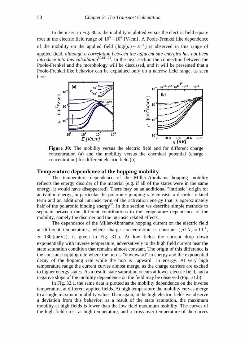
58 Chapter 2- The Transport Calculation
In the insert in Fig. 30.a. the mobility is plotted versus the electric field square root in the electric field range of . A Poole-Frenkel like dependence of the mobility on the applied field (
5 610 10 [V/cm]−
( ) 1 2log Eµ ∼ ) is observed in this range of applied field, although a correlation between the adjacent site energies has not been introduce into this calculation80,81,121. In the next section the connection between the Poole-Frenkel and the morphology will be discussed, and it will be presented that a Poole-Frenkel like behavior can be explained only on a narrow field range, as seen here.
105 106 107 108
10-6
10-5
10-4
E [V/cm]
µ [
cm2 /V
sec]
1000 2000
10-6
10-5
E1/2
µ(a)
-1 -0.8 -0.6 -0.4 -0.210-7
10-6
10-5
10-4
η [eV]µ
[cm
2 /Vse
c]
p1010 1012 1014 1016 1018
(b)
Figure 30: The mobility versus the electric field and for different charge concentration (a) and the mobility versus the chemical potential (charge concentration) for different electric field (b).
Temperature dependence of the hopping mobility
The temperature dependence of the Miller-Abrahams hopping mobility reflects the energy disorder of the material (e.g. if all of the states were in the same energy, it would have disappeared). There may be an additional "intrinsic" origin for activation energy, in particular the polaronic jumping rate consists a disorder related term and an additional intrinsic term of the activation energy that is approximately half of the polaronic binding energy63. In this section we describe simple methods to separate between the different contributions to the temperature dependence of the mobility, namely the disorder and the intrinsic related effects.
The dependence of the Miller-Abrahams hopping current on the electric field at different temperatures, where charge concentration is constant ( 4/ 10Vp N −= ,
=130 [meV]σ ), is given in Fig. 31.a. At low fields the current drop down exponentially with inverse temperature, adversatively to the high field current near the state saturation condition that remains almost constant. The origin of this difference is the constant hopping rate where the hop is "downward" in energy and the exponential decay of the hopping rate while the hop is "upward" in energy. At very high temperature range the current curves almost merge, as the charge carriers are excited to higher energy states. As a result, state saturation occurs at lower electric field, and a negative slope of the mobility dependence on the field may be observed (Fig. 31.b).
In Fig. 32.a. the same data is plotted as the mobility dependence on the inverse temperature, at different applied fields. At high temperature the mobility curves merge to a single maximum mobility value. Than again, at the high electric fields we observe a deviation from this behavior; as a result of the state saturation, the maximum mobility at high fields is lower than the low field maximum mobility. The curves of the high field cross at high temperature, and a cross over temperature of the curves

Chapter 2- The Transport Calculation 59
(T0) can be observed. We note that if the observation did not include the high temperature values, an extrapolated value of a cross over temperature is observed even from moderate and low field data. Commonly, the T0 temperature, and the negative slope that is observed beyond this temperature (or expected to be observed) is assumed to relate to the inversion region of the polaronic jumping rate63 (Eq. (1.1.33)), and to the polaron binding energy. Nevertheless, in our plot the polaronic effect was overlooked as we examined the Miller-Abrahams hopping currents. We conclude that an extrapolated T0 or a high field observation of T0 are not good indicators for the polaronic mechanism. On the other hand, the current on the hopping mechanism is monotonically increases with applied field (at least, stay constant). For that reason, a negative slope of the current with the applied field (as seen in Refs.76,122) may indicate on the polaronic effect on the jumping process. Finally, we note that the T0 that is observed due to the state saturation effect causes different observed crossover temperature values at different charge concentration (Fig. 32.b). This may serve as an indication on the origin of the observed (extrapolated) cross over temperature, and distinguish between polaronic and disorder related effects. The polaronic related cross over temperature is intrinsic to the jumping mechanism and is not expected to vary with charge concentration (as long as the binding energy does not depend on charge concentration).
10-3 10-2 10-1 100
10-10
10-8
10-6
E [V/R0]
J [a
.u.]
100 150 200 250 300 350 400 500 600 700 800 900 1000
T [oK]
(a)
10-3 10-2 10-1 100
10-2
10-1
100
E [V/Ro]
µ [a
.u.] 100
150 200 250 300 350 400 500 600 700 800 900 1000
T [oK]
(b)
Figure 31: Miller-Abrahams hopping current (a) and mobility (b) versus the applied field at different temperatures, ( =130 [meV]σ , ) 4/ 10Vp N −=
0 0.002 0.004 0.006 0.008 0.01 0.012
10-2
10-1
100
1/T [oK]
µ [a
.u.]
2*10-3
4*10-3
8*10-3
1.7*10-2
3.3*10-2
6.6*10-2
0.130.260.531
E [V/R0]
(a)
10-10 10-8 10-6 10-4 10-2400
500
600
700
800
900
1000
1100
p/NV
T 0 [o K]
(b)
Figure 32: Miller-Abrahams mobility dependence upon the inverse temperature for a given charge concentration ( 4/ 10Vp N −= ) and different electric fields (a). The cross over temperature (T0) as determined by the cross section of mobility versus field curves at different charge concentration (b) ( =130 [meV]σ ).

60 Chapter 2- The Transport Calculation
Next, we examine the influence of charge carrier concentration and the electric field on the activation energy of the hopping mobility, near room temperature (Fig. 33). Since the transfer rate of the model is in the Miller-Abrahams form the only possible origin of the activation energy is the energy disorder (contrary to other possible contribution as the polaronic effect). We find that an increase of the applied field and/or the charge concentration decreases the activation energy from ~250 meV to ~30 meV. We note that the activation energy in the polaronic model is constituted from the energy disorder contribution and half of the polaronic energy. However assuming the hopping mechanism is polaronic, an increase in the electric field results in a decrease in the hopping rate (in the inversion region) or at least expected to change the intrinsic activation energy. On the other hand, the relation between the polaron binding energy and the charge concentration is expected to be less profound, and assuming the intrinsic activation energy does not depend on the charge concentration. For that reason, we suggest measuring the intrinsic activation energy in the high concentration range, where the disordered related activation energy diminished. The dependence of the activation energy on the charge concentration explains another difference between FETs and LEDs. The difference of ~200 meV between "low concentration" (LED) mobility activation energy and "high concentration" (FET) activation energy was measured by us123-125 (215±10 meV and 400±40 meV in MEH-PPV based FET and LED, respectively) and in Ref. 106. However, the activation energy measured at high concentrations (FET) is significantly higher than the GDM, Miller-Abrahams model prediction, indicating an additional source for the activation energy besides the energy disorder. Therefore, at high concentration measurement, where the energy disorder contribution is negligible, the polaronic binding energy can be estimated as twice the measured activation energy (~390-430 meV for MEH-PPV at the previous example). More details on the activation energy measurements in FETs are given in section 3.2.2.
105 106 1070
0.05
0.1
0.15
0.2
log(E) [V/cm]
EA
[e
V]
1010
1014
10180
0.15
0.3
p [cm-3]
EA
[eV
]
1015 [cm-3]
1016 [cm-3]
1017 [cm-3]
1018 [cm-3]
1019 [cm-3]
Figure 33: The activation energy of the mobility versus the electrical field for different charge concentration (for DOS width =130 [meV]σ , NV=1020 [cm-3] and Miller Abrahams transfer between sites). While at high electrical fields the activation energy is low for any charge concentration, the activation energy at low electrical field (plotted in the insert) is strongly dependent on the charge concentration. At high charge concentration the activation energy originated on energy disorder strongly decreases, resembling that the measured high concentration activation energy has a different origin.

Chapter 2- The Transport Calculation 61
Mobility dependence on the density of states Here we examine the role of the exact DOS on the mobility dependence upon
electric field and charge concentration. We demonstrate that charge concentration dependence of the mobility is a sensitive measure to the DOS exact shape. Moreover, we demonstrate that the field dependence of the mobility does not reflect the DOS shape at reasonable DOS widths and charge concentration conditions. As a result, the widely used Poole-Frenkel exponential factor analysis by Bassler's diluted system mobility equation8 may lead to underestimation of the DOS width.
From the low field linearization of the mobility (Eq. (2.4.5)) we concluded that the low field mobility depends only on the exact shape of the DOS and the equilibrium distribution function. We emphasize that at low fields the jumping mechanism can be linearized as well, as long as the envelope function (Eq. (1.1.30)) does not vary with energy to fast. Therefore, the exact assumption of the jumping mechanism is not expected to modify the mobility dependence upon the charge concentration, apart from multiplying the mobility by a factor. As demonstrated in the next chapter, the exact morphology is expected to have the same effect for reasonable 3D sites arrays. In figure 34 we demonstrate the close relation between the exact DOS and the mobility dependence on charge concentration. In this figure we plot the mobility versus the charge concentration for three models of DOS: a single gaussian ( 5σ = ), and three examples of double gaussian DOS, where the centers of the gauss bells are located at different energies. Where additional states are added below the center of the gaussian (dotted and dashed dotted lines), the mobility dependence on the charge concentration is modified even when the additional deep states concentration is low (in this example 1% of the states are deep states). The change is clearly seen at the low-to-moderate charge concentration region. On the other hand, added states near or above the gaussian DOS centre (dashed lines) influences the mobility only when the added states are the high concentration range. This situation is not reasonable at the variable range hopping model, but it is similar to a situation that a mobility edge exist at the upper part of the gaussian. In both cases, namely when a mobility edge exist or when we added an artificial narrow pick in the DOS, charge carriers that are at high enough energy acquire significantly higher mobility. The conclusion of this example is that the mobility dependence on the charge concentration is a sensitive probe to low-energy states at low concentrations ("trap" like states), and the lower energies DOS shape. In order to examine whether a mobility edge exist one should increase the charge concentration to a level that all of the localized states are filled. Namely, the existence of a mobility edge is examined only at extremely high charge concentrations.

62 Chapter 2- The Transport Calculation
-30 -20 -10 0 10 20 30
10-10
10-5
100
ε [kT]
g(ε)
[a.u
.]
σ=5 εo=0σ1=1 εo,1=(-15) N
T=0.01
σ1=1 ε
o,1=(-20) N
T=0.01
σ1=1 ε
o,1=2 N
T=10
(a)
-40 -30 -20 -10 010-3
10-2
10-1
100
101
η [kT]
µ [a
.u.]
σ=5 εo=0σ1=1 εo,1=(-20) N
T=0.01
σ1=1 ε
o,1=2 N
T=10
σ1=1 ε
o,1=(-20) N
T=0.01
(b)
10-15 10-10 10-5 10010-3
10-2
10-1
100
101
log(p)
µ [a
.u.]
σ1=1 εo,1=(-15) NT=0.01
σ=5 εo=0
σ1=1 ε
o,1=(-20) N
T=0.01
σ1=1 ε
o,1=2 N
T=10
(c)
Figure 34: The mobility versus chemical potential (b), and versus the charge carrier concentration (c) for different DOS shapes (a): A single DOS (solid line), Deep traps, two gaussian model (and dotted and dashed –doted lines). (c) "Mobility edge" like two gaussians model (dashed line). 0,, and Vi i iN σ ε are the state concentration, DOS width and DOS centre of the ith gaussian, respectively.
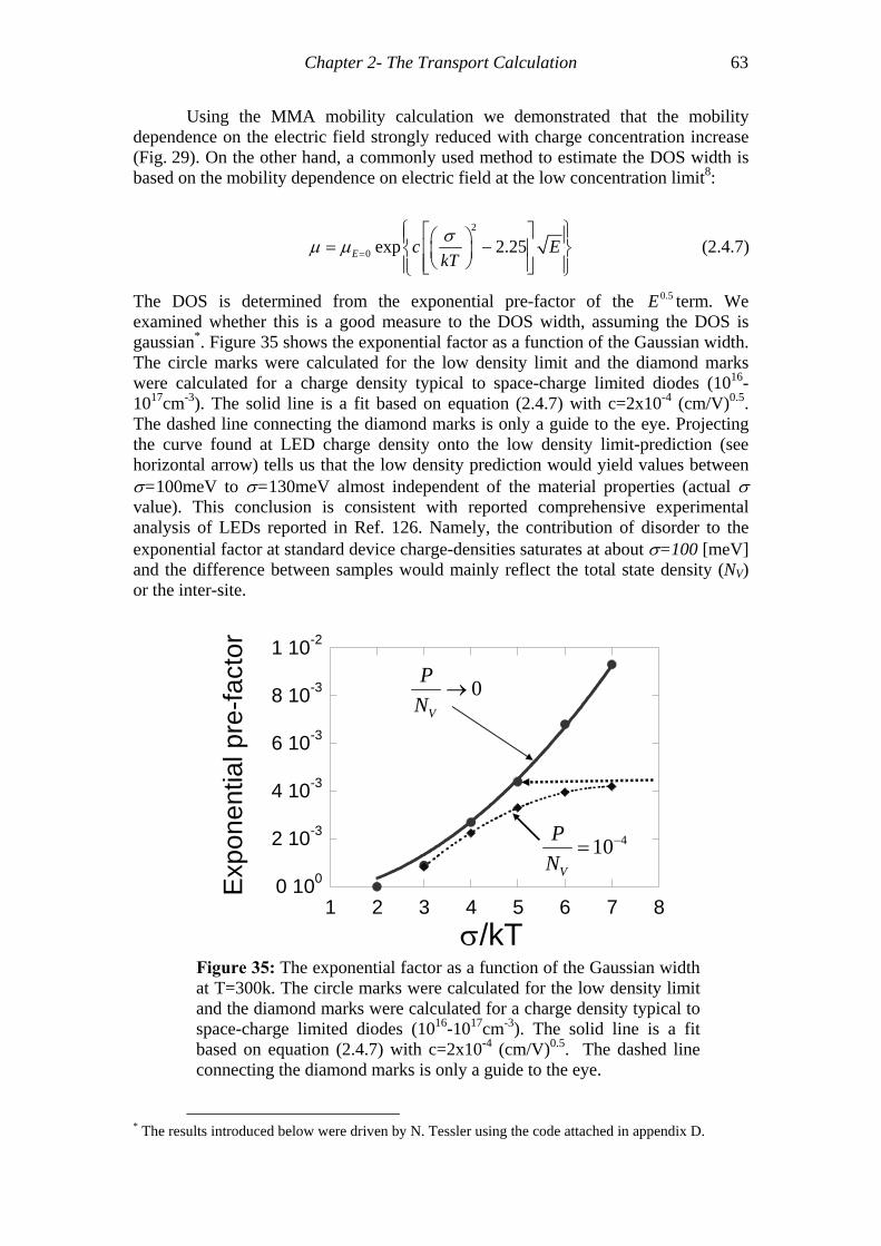
Chapter 2- The Transport Calculation 63
Using the MMA mobility calculation we demonstrated that the mobility dependence on the electric field strongly reduced with charge concentration increase (Fig. 29). On the other hand, a commonly used method to estimate the DOS width is based on the mobility dependence on electric field at the low concentration limit8:
2
0 exp 2.25E ckTσµ µ = E
⎧ ⎫⎡ ⎤⎪ ⎪⎛ ⎞= −⎢ ⎥⎨ ⎬⎜ ⎟⎝ ⎠⎢ ⎥⎪ ⎪⎣ ⎦⎩ ⎭
(2.4.7)
The DOS is determined from the exponential pre-factor of the term. We examined whether this is a good measure to the DOS width, assuming the DOS is gaussian
0.5E
*. Figure 35 shows the exponential factor as a function of the Gaussian width. The circle marks were calculated for the low density limit and the diamond marks were calculated for a charge density typical to space-charge limited diodes (1016-1017cm-3). The solid line is a fit based on equation (2.4.7) with c=2x10⁻⁴ (cm/V)0.5. The dashed line connecting the diamond marks is only a guide to the eye. Projecting the curve found at LED charge density onto the low density limit-prediction (see horizontal arrow) tells us that the low density prediction would yield values between σ=100meV to σ=130meV almost independent of the material properties (actual σ value). This conclusion is consistent with reported comprehensive experimental analysis of LEDs reported in Ref. 126. Namely, the contribution of disorder to the exponential factor at standard device charge-densities saturates at about σ=100 [meV] and the difference between samples would mainly reflect the total state density (NV) or the inter-site.
0 100
2 10-3
4 10-3
6 10-3
8 10-3
1 10-2
1 2 3 4 5 6 7 8
0V
PN
→
410V
PN
−=
σ/kT
Exp
onen
tial p
re-fa
ctor
Figure 35: The exponential factor as a function of the Gaussian width at T=300k. The circle marks were calculated for the low density limit and the diamond marks were calculated for a charge density typical to space-charge limited diodes (1016-1017cm-3). The solid line is a fit based on equation (2.4.7) with c=2x10⁻⁴ (cm/V)0.5. The dashed line connecting the diamond marks is only a guide to the eye.
* The results introduced below were driven by N. Tessler using the code attached in appendix D.

64 Chapter 2- The Transport Calculation
In order to find a more reliable and a simple measure to the DOS we examine the mobility dependence upon charge concentration (Fig. 36). Note that the density dependence at the relatively high range (above 1017 [cm-3]) resembles a power law ( ), but the coefficient is electric field dependent. For example, for σ=4kT the low field and high field exhibit a power law of κ=0.33 and κ=0.11, respectively. For σ=7kT the low field and high field exhibit a power law of κ=0.62 and κ=0.28, respectively. We have calculated κ for a range of DOS widths (see Fig. 37) and at the low field regime. It was found that it could be numerically fitted using
Pκµ ∝
=0.73-1.17 exp1.65kT kT
σ σκ ⎛⋅ ⋅ −⎜ ⋅⎝ ⎠⎞⎟ . Namely, for a system described by a single
Gaussian DOS the maximum slope is κ= 0.73 and it is close to this maximum at σ=8kT. It has been suggested that organic films are composed of domains that would make the effective density of states a bit more complicated then a single Gaussian124,127-130. Following the notion in Ref. 124 we also show in figure 37 the slope found for a DOS that is a linear combination of two Gaussians having σ=8kT and σ=12kT centred at the same energy(1:1 composite).
10-2
10-11014 1015 1016 1017 1018 1019
10-5
10-4
10-3
10-2
10-1
10-6 10-5 10-4 10-3 10-2 10-1
5.5x10⁵
≤1x10⁵
5.5x10⁵
≤1x10⁵
Mob
ility
(a.u
.)
Relative Charge Density
Charge Density (cm-3)
σ=4kT
σ=7kT
(A)
(B)
Figure 36: The calculated mobility as a function of charge density at T=300k. The lowest curve is for low electric fields.

Chapter 2- The Transport Calculation 65
0
0.2
0.4
0.6
0.8
1
0 5 10 15 20
/ kTσ
κ
1 18 122 2σ σ+
Figure 37: The dependence of the power law coefficient (κ) on the DOS width σ/kT for the low electric field regime at T=300k.
Hopping rate from a given initial site
Here we examine the validity of common approximations for hopping transport at practical conditions. In figure 38 we plot the hopping probability from a given site i which lies near the chemical potential to all of the states near a final energy jε ( 5, 25, 25iσ η βε= = − = − ). It is clear that for all conditions, low temperature approximations that assume that all of the transport occurs near Fermi-level (as the Kubo-Greenwood approximation17) will fail in this system as the charge carrier maximum probability hop is far from the chemical potential. This stems from the similarity between the typical DOS width and the temperature ( ). At the low field limit a linearization of the hopping rate may be applied (see appendix D), as visualized by the similar shape of the forward and backward hopping rate dependence on distance and final energy (a). At the intermediate (c) and strong (d) field range the hopping linearization fails, as the backward hopping diminished and the forward hopping curves vary in shape with the applied field: in the state saturation region (d), the potential drop due to the strong applied field lower all of the final states below the initial state and the hopping probability shape reflects the shape of the DOS. In the intermediate range of fields (c) an interesting phenomenon occurs: the long distance hops contribute more than the typical distance (localization radii) jumps. This results in a needle shape of the hopping surface. This shape is very sensible to the exact DOS shape and the applied field, as it stems from the balance between the increase concentration of states at the level of the initial state and the hopping decay in space. At this range any approximation that does not depend strongly on the exact DOS shape fails.
kT
Another approximation that is widely used for diluted systems and a gaussian DOS are the effective transport energy95. In the effective transport energy approximation it is assumed that the carrier that contribute the most to the current jump from a small range of energy (for diluted systems the effective energy is σ−∼ . We calculated the maximum current energy at different charge concentration and

66 Chapter 2- The Transport Calculation
found that it increases with increasing charge concentration (not presented here, see Ref. 117). Finally, the effective temperature approximation that assumes that the distribution function can be described in term of effective heating of the charge carrier to an effective temperature 45 and the effective temperature 88,131 will be examined in section 2.5.2, where a direct solution of the Master equation is presented.
*-5 0 5 10 γR-25
-15
0
15
E/kT (a)
*-5 0 5 10 γR-25
-15
0
15
E/kT (b)
*-5 0 5 10 γR-25
-15
0
15
E/kT (c)
*
-5 0 5 10 γR-25
-15
0
15
E/kT (d)
10-2
10-1
100
101
102
10-6
10-5
10-4
10-3
10-2
E [γ/β]
Eff
ectiv
e m
obili
ty fr
om si
te i
[a.u
.]
a b
c
d
(e)
Figure 38: The hopping probability from a given site i to a final energy jε at different applied fields (a-d). The applied field and the current from site i is marked on the effective mobility for charge carrier at energy iε curve (e). The initial site is marked by a star and the current to a given final energy and distance is presented by the color. The background color is insignificant. ( 5, 25, 25iσ η βε= = − = − )

Chapter 2- The Transport Calculation 67
2.5 Mobility in Calculation for Realistic Spatial Site Distribution - The Effect of Morphology
Up till now we examined the mobility under the assumption of homogenous medium, i.e., each point in space contained all of the DOS. In this section we examine the effect of realistic spatial distribution of the conjugated segments in space. We begin by examining the effect of realistic conjugated segments morphology in the framework of MMA and we demonstrate that as long as the MMA is valid, the mobility can be described by a master curve and multiplied by morphology related factors. Next we examine the direct solution of the full Master equation, and we demonstrate the close relation between the topology of the nearest neighbors segments network and the validity of the MMA.
2.5.1 Inhomogeneous Solution of the Mean Medium Approximation
In this section we examine the influence of a realistic morphology, namely spatial conjugated segments distribution, the mobility under the assumption that the MMA holds. Explicitly, we keep the assumptions that a local equilibrium exists, and the each point contains whole of the DOS. Nevertheless, we assume that a short range order exists, as a result of structural constrains as minimum insulating distance (e.g. side chains length), molecules structure and typical packing dimensions. It is convenient to describe the morphology radial correlation function as it serves as a bridge between the measurement or the model of the structure of the amorphous semiconductor and the calculation of the charge carrier transport properties. Assuming an isotropic material without any preferred direction, the radial correlation function is defined as132*:
( ) ( )( )
24 V
P RR
R Nρ ρ
π
== =
ij
ij
RR (2.5.1)
A typical shape of a realistic site distribution and the equivalent radial distribution is given in figure 39. The typical radial distribution function zeros at short distances
( )ρ R
R
1 n.n.2 n.n.
( )ρ R
R
( )ρ R
R
1 n.n.2 n.n.
Figure 39: A schematic description of realistic site distribution and the equivalent radial correlation function. The grey circles and the grey painted peaks present the first and second nearest neighbors location.
* We use ( )Rρ rather than the commonly used ( )g R as denotes the DOS in this work. In addition, we use the normalized (reduced) radial correlation function as defined in Ziman's book
g129.

68 Chapter 2- The Transport Calculation
below a minimum distance between adjacent sites. In the intermediate range there are several peaks that represent the typical distance for the (first, second) nearest neighbors (n.n.), and the long limit of the radial distribution function is a unity, as the correlation between the locations of the different sites disappears.
The calculation of the inhomogeneous MMA current for a given spatial distribution is similar to the homogenous MMA calculation, where the homogenous integrand is multiplied by the radial correlation function:
( ) ( ) ( ) ( ) ( )
( )
, , ,
ˆ1 ,
i j ij i j i i j
j
d d d g f g
f
ε ε ρ υ ε ε ε ε η ε
ε η
∞ ∞
ℜ −∞ −∞
= −
⎡ ⎤− − ⋅ ⋅⎣ ⎦
∫ ∫ ∫ij ij ij ij
ij ij
J R R R R E
R E R E
⋅ (2.5.2)
As we assumed that the correlation function is radial (isotropic medium), and assuming the jumping mechanism is isotropic, (namely it depends on the absolute distance and the final and initial energies - but not on the direction) the current integral can be written as 1D in space (appendix C.1.):
( ) ( )
( ) ( )( ) ( )
0
0
2 , ,
where exp
i j i j
S
z
dz d d z z
R Lz R dR R
R
π ε ε ε ε
ρ ρ
∞ ∞ ∞
−∞ −∞
∞
= Ω
⎛ ⎞−= = −⎜ ⎟
⎝ ⎠
∫ ∫ ∫
∫
J
R (2.5.3)
A general method to solve the current equation is described in appendix C.1. Here we concentrate on the Miller-Abrahams hopping mobility. For simplicity we assume that the conjugated segments that are surrounded by an insulator (e.g. the inert side chains of the conjugated polymers) can be described by a model of hard spheres with metallic core of a diameter LS and insulating shell (Fig. 40), and the variations in the core size are neglected. The correlation function for this model rises sharply near the sphere diameter (LS+BS). A reasonable approximation for this model is a step function:
( ) ( )S SR R L Bρ θ≅ − − (2.5.4)
The Miller-Abrahams hopping mobility is calculated by inserting Eq. (2.5.4) into the current equation, (Eq. (2.5.3)). The numerical algorithm to perform this calculation is given as a Matlab code in appendix D. A linearization of the current equation for low electric field ( ( )0S SL B R E kT+ + ) where the localization radius is smaller than the typical morphological dimensions 0 ,S SR B L is given in appendix C.2. This linearization result in a scaling low of the low field mobility with the morphological parameters:
3
0 hom 0
0 0hom
expE in ogenoues S S S
E ogenoues
L B R B
0R R
µ
µ→
→
⎛ ⎞ ⎛+ +≅ ⎜ ⎟ ⎜
⎝ ⎠ ⎝
⎞− ⎟
⎠ (2.5.5)
In figure 41 the result of the linearized mobility scaling low and the full numerical calculation for the low field condition are plotted. The full calculation is similar to the linearization result, apart from the low BS and LS region where the actual scaling nominator is slightly higher than 3 (see explanation in appendix C.2). However, each point of the full calculation represents a calculation of the full field

Chapter 2- The Transport Calculation 69
and concentration range (Fig. 42). The result of this calculation is a master curve that describes the mobility in the full electric field, charge concentration and morphological parameters range: the low field mobility scaling is described above and the electric field in the master curve is normalized to the typical distance of the system, ( )0S SE E L B R= + + . Applying typical parameters ( ,
and ) result in a wide range of scaling parameter (~0.001-100) which may explain the wide range of measured mobility where the morphology varies (e.g. see below section 3.2.2 and Ref. 124).
0 0.1 0.2 [nm]R = −
0.5 2 [nm]SB = − 1 3 [nm]SL = −
Up till now we examined inhomogeneous radial correlation function, nevertheless the medium remained homogenous in a sense that the typical properties do not vary in space. Here we briefly discus the influence of spatially inhomogenity in the conjugated polymer layer. A short range variation in the morphology that influences localization radii and insulator width, can be described in term of a modified radial distribution function, and are not expected to modify the results significantly. On the other hand, a long range spatial variation of the morphology may extend the mobility dependence on the electric field to a wider range of electric-fields: When the morphological parameters are constant in space, the mobility is constant at the low electric-field range and increases sharply near a typical electric-field of the thermal energy over the typical dimension of the system, ( )0/ S SkT q L B R+ +⎡ ⎤⎣ ⎦ . The sharp increase in the mobility occurs in a narrow range of approximately one decade in the field (e.g. Fig. 42), and a Poole-Frenkel like mobility ( ( )1 2~ exp A Eµ ⋅ ) can describe the mobility merely at a narrow range of electric field. When the morphological parameters vary in space (at long ranges) a single typical dimension cannot represent the morphology, and the dependence of the mobility on the electric field weakens, and a Poole-Frenkel like equation may describe the mobility across a wider range of electric field. In order to examine this argument, we estimate the reasonable variation in the different morphological parameters: It is reasonable to assume that the size of the conjugated segments core do not disperse more than one order of magnitude (e.g. ~2-20 nm), and the minimum insulator width varies no more than that. The localization radii that is determined by the height of the potential barrier between sites, varies by no more than a factor of two, assuming the barrier height do vary more than twice. As a result the mobility field dependent range may be extended
( )ρ R
R
( )ρ R
R
( )ρ R
R
( )ρ R
R
Figure 40: Hard sphere model of conjugated polymer: the conjugated segments are equivalent to the metallic core (black), and the side chains are equivalent to the insulating shell (white). The correlation function for this model can be approximated to a step function that rises at the minimum insulating width.

70 Chapter 2- The Transport Calculation
from one decade to ~2-3 decades ( . As the mobility Poole-Frenkel dependence was found to be valid on a wider range in some of the amorphous organic semiconductors, the variation in morphological parameters cannot be referred as a general reason for the Poole-Frenkel dependence and other explanations, as the energy correlation between adjacent sites has to be considered
5 710 10 [V/cm]−
80,81,83.
(a) (b)(a) (b)
Figure 41: The calculated low field mobility versus the minimum width insulator width- BS (a), and the typical dimension of the system - 0S SL B R+ + (b). The mobility was calculated by the low field linearization (dashed line) and by the numerically by the full calculation (dotes). Each dote represent one full calculation of mobility in the full range of electric field and charge concentration as demonstrated in the next figure.
104
105
106
107
10-4
10-3
10-2
Ls=1Bs=0
E [V/cm]
µ [c
m2 V
-1se
c-1]
104
105
106
107
10-6
10-5
10-4
10-3
Ls=1Bs=1
E [V/cm]
µ [c
m2 V
-1se
c-1]
104
105
106
107
10-8
10-7
10-6
10-5
Ls=1Bs=2
E [V/cm]
µ [c
m2 V
-1se
c-1]
104
105
106
107
10-10
10-9
10-8
10-7
Ls=1Bs=3
E [V/cm]
µ [c
m2 V
-1se
c-1]
Figure 42: Full calculation of the mobility in a full range of electric field and charge concentration for different morphological parameters. Each of the curves is equivalent to one of the points in the former graph.

Chapter 2- The Transport Calculation 71
2.5.2 The discrete master equation direct solution The calculation of the transport properties, in the previous sections, relies on
the assumption that the system is near equilibrium. In this section we examine the validity of this assumption by demonstrating the close relation between the topology of the hopping sites network and the local equilibrium condition. In contrast to the previous sections, we open this discussion by an example: A comparison between the MMA mobility calculation and an accurate calculation for a specific system (1D). Afterwards we will present a method to rationalize the inconsistency that arises from the first example, namely a direct solution of the transport properties for specific morphologies.
The hopping mobility had not been calculated analytically for most of the reasonable site distributions, and the solution of these systems was performed in a framework of an approximation or by numerical calculation (e.g. Monte-Carlo simulation8). However, the diluted system mobility was calculated for one specific configuration of the hopping sites, namely 1D array, Derrida's formula82. In figure 43 we compare the MMA calculated mobility to the 1D analytical solution, where the DOS width was kept constant in both calculations ( 5σ = ). The mobility at the site saturation region (high fields) was used to equalize the units of the different solutions, as in this region the current is 1D even in 3D systems74. The low field mobility varies between these solutions by eight orders of magnitude denoting the MMA is not a reasonable approximation for the 1D system. An intuitive explanation to this difference is by translating all of the hopping processes between the different sites to resistor network. In the 1D system the slowest process (the biggest resistor) determines the current, while in the MMA we assume that each site consists all of the possible energy levels and it is equivalent to a parallel resistor network were the fastest hopping rate (the smallest resistor) determines the current. The 1D solution will describe the current near percolation and sometimes is referred as the percolation path approximation (PPA). We may think about the difference between these morphologies by examining a topological measure of the system: the number of nearest neighbors (n.n.). While in the 1D system there are only 2 n.n. (Fig. 44.a) in the MMA there is an infinity number n.n. (Fig. 44.c). A realistic 3D configuration is between these limits: The maximum number n.n. in 3D pacing of equivalent spheres is 12 (FCC or HCP lattices). A more reasonable model for amorphous systems is a
104 106 10810-14
10-12
10-10
10-8
10-6
10-4
E [V/cm]
µ [a
.u.]
Mean Medium Approximation
Accurate 1D Calculation*
Figure 43: A comparison between the MMA calculation (described above) of the mobility and the accurate calculation of the mobility in 1D system by Derrida's formula82.

72 Chapter 2- The Transport Calculation
close random packing that leads to 5-8 n.n. Here we examine the question, can we describe the realistic system mobility by one of these approximations? (Is the behavior of 5-8 n.n. system is closer to 2 n.n. or to ∞ n.n?)
(a) (b) (c)(a) (b) (c)
Figure 44: The number of nearest neighbors (n.n.) in different systems: 1D system – 2 n.n. (a), A schematic description (2D plot) of close random packed 3D system – 5-8 n.n.(b), mean medium approximation ∞ n.n. (c).
In order to solve the realistic system behavior, we solved the steady state
Master equation directly, for a realistic site distribution. The method of the solution is the following: The hopping current was determined by the Miller-Abrahams condition. We calculated the result of the steady state Master equation (Eq. (2.2.1))
( ) ( ) ( ) ( )''
0 1 1 'ji ijj j
P j P i P j P iυ υ⎛ ⎞
= − − −⎡ ⎤ ⎡ ⎤⎜ ⎟⎣ ⎦ ⎣ ⎦⎝ ⎠
∑ ∑
For diluted system were the Master equation can be linearized and written as a Markov chain:
( ) ( )''
0 ij jij j
P i P jυ υ⎛ ⎞
= − +⎜ ⎟⎝ ⎠∑ ∑ (2.5.6)
The first term is the diagonal terms of and the second is the off-diagonal terms in the algebric form of the equation (see Eqs. (1.1.4) and (1.1.5)):
( ) where , 1ij
ijj i
ii j i j
υυ
≠
=
j∈ ≠⎧⎪= ⎨ − ∈ =⎪⎩
∑
P ΩP
Ω (2.5.7)
The solution of the Master equation is the eigen vector P of matrix that corresponds to the eigen value of unity. We used a given configuration in space: 1D equally spaced site array and a result of 3D molecular dynamic calculation of packing of hard spheres in a box (Fig. 45). The energy of the different sites was determined by randomized value from a gaussian probability density function with a width of 5kT. The applied field was inserted as a potential drop along the field direction, and we used cyclic boundary conditions for the hopping currents.
Ω
In figure 46 the calculated mobility from two typical 3D runs is plotted versus
the applied field. While at the high electric field the mobility of the different runs merges, the low field mobility varies significantly between the different runs. The reason for this difference between the runs is the finite size of the system (928 sites) that determines an effective cutoff to the DOS. As the probability to randomize a low

Chapter 2- The Transport Calculation 73
(a)
(b)
0 1 2 3 4 5 6 7 80
1
2
3
4
5
|Rij| [ball radii]
ρ (|R
|)
System size
Figure 45: A 3D plot of (part of) the matrix of the close random packed spheres (a), and the equivalent calculated radial correlation function (b) used for the Master equation direct solution. The drop in the correlation function beyond 4.5 spheres radii is the result of the maximum distance allowed in the simulation.
energy state is low, the lowest energy state (marked by an arrow in the insert in Fig. 46) of a certain ensemble varies significantly. The low field mobility is a sensitive indicator for the exact DOS shape (see Eq. (2.4.5)) and changes significantly by the "effective cutoff". We note that in a real short device (as LED or photovoltaic cells) this effective cutoff is expected to occur as the total device width is approximately 50-100 sites long. The effective cutoff plays a similar role to the filling of the lowest states at none-diluted systems, where the highest filled state is approximately at the chemical potential. We expect an MMA calculation to follow the Master equation result when the chemical potential is determined near the effective cutoff energy of the specific ensemble. Explicitly, the Master equation calculated mobility is always higher than a diluted system solution. However if we increase the chemical potential up to the lowest randomized state level, the filled states in the MMA calculation are equivalent to the non-existing states in the specific ensemble (as deduced from the numerical calculation, see examples in Fig. 46). Therefore the mobility in both calculations is expected to be similar.
Another measure to the validity of the local equilibrium assumption is occupation probability of the different sites, P(i). We plotted the occupation probability versus the sites energy for the different solutions (1D and 3D). As we solved a diluted system, we expect the probability of the sites to follow the Boltzmann condition where the system is near equilibrium. We emphasize that we use the Miller-Abrahams hopping equation that contains the detailed equilibrium condition and drives the system toward equilibrium. On the other hand the applied field adds energy to the charge carrier and may drive the system out of equilibrium. For example the occupation probability in the 1D system without an applied field follow exactly the Boltzmann condition (Fig. 47.a), as all systems are expected to be at equilibrium without an external interference. However, when we applied field on the 1D system, the occupation probability of the sites deviates from the Boltzmann condition significantly (at electric-fields beyond ~104 [V/cm], where Rn.n.=2 [nm]), denoting the invalidity of the local equilibrium assumption. We note that the MMA fails even at lower electric fields, where the local equilibrium assumption is valid, as the mobility calculation demonstrated).

74 Chapter 2- The Transport Calculation
104 105 106 107 10810-6
10-5
10-4
E [V/cm]
µ [a
.u.]
-15 0 15ε [kT]
# of
sta
tes
-15 0 15ε [kT]
MMA η=-20
MMA η=-25
MMA η<-35
Figure 46: The calculated mobility from the Master equation solution (marked lines) of two representative runs, and the result of the MMA calculation at different chemical potential values (solid lines). The histogram of the randomized energies of the Master equation runs is given in the insert, where the lowest energy state is marked by an arrow.
Similarly to the 1D system, the occupation probability in the 3D system follows exactly Boltzmann condition without an applied field (Fig. 48). On the other hand, when the applied field approaches (for field values higher than
where r is the spheres radii), the occupation probability start to deviate from Boltzmann approximation. The occupation probability, namely the non-equilibrium distribution function behaves almost by Boltzmann distribution with an effective temperature that depends on the applied field, similarly to Shklovskii effective temperature prediction
/ 2kT r0.4 / 2kT r⋅
88, that summarized numerical examination of exponential DOS Master equation solution. Nevertheless this change in the charge carrier distribution almost does not change the mobility, as can be explained by the following arguments: 1) at low field the charge carrier distribution is the equilibrium distribution, and at high field the Miller-Abrahams current saturates. As a result both of the low field and high field mobility are expected to be calculated correctly by the MMA. Therefore, the change in the mobility is limited to the narrow field range between and ~ 0.5 / 2kT r⋅ ~ 10 / 2kT r⋅ . 2) the effective temperature is a charge distribution-temperature which is not directly related to the thermal energy dictated by the lattice. 3) The activation energy at the high field range (and with the low state effective filling determined by the "cutoff energy") is much lower than the low field activation energy (~5 meV, see Fig. 33). As a result the charge carrier distribution changes at the field range that it does not influence the mobility any longer, and the mobility is expected to be calculated correctly by the MMA at all field range. We note the other transport properties may change due to the effective temperature change, which for r=1nm starts to occur at 105Vcm-1 (e.g., the diffusion coefficient, in the transverse direction to the applied field is determined by the charge distribution and is expected to increase due to the effective temperature increase). On the other

Chapter 2- The Transport Calculation 75
hand, the polaronic jumping rate is not expected to change due to the effective temperature change, as the actual temperature (the phonon temperature) is not changed (directly) by the applied field.
Finally, we note that the low field, long time limit occupation probability was calculated by Monte-Carlo simulations of Miller-Abrahams hopping in a gaussian DOS array8 (Fig. 13). After a certain time the charge carrier temporal distribution was found to equilibrate into the gaussian shape distribution (termed in the reference as "dynamical equilibrium"), which stems from the Boltzmann equilibrium distribution. This result supports using the Master equation as an accurate solution for the transport calculations, although this solution ignores possible correlations between temporary occupations of adjacent sites ("jamming").
(a)
-8 -6 -4 -2 0 2 4 6 810-8
10-6
10-4
10-2
100
ε [kT]
Occ
upat
ion
prob
abilit
y
0 [V/cm]Boltzmann dist.
Constant Concentration
MMA - Boltzmann Distribution
(b)
-8 -6 -4 -2 0 2 4 6 810-8
10-6
10-4
10-2
100
ε [kT]
Con
cent
ratio
n pr
obab
ility
00.10.5210
kT/q|Rn.n.|
Figure 47: The occupation probability factor of the sites in 1D system. While the zero field occupation probability follows Boltzmann distribution (a), the occupation probability deviates significantly from Boltzmann distribution even at moderate fields (b).
-20 -10 0 10 2010-20
10-15
10-10
10-5
100
E [kT]
Con
cent
ratio
n pr
obab
ility
00.10.40.81.21.62351040
Electric field [kT/2r]
Boltzmann distribution
Figure 48: The occupation probability factor of the sites in 3D system. The occupation probability follows Boltzmann distribution at applied field below 0.4 / 2kT r⋅ .

76 Chapter 2- The Transport Calculation
2.6 Summary and Discussion In this chapter we presented a unified calculation method for variable range
hopping of diluted and non-diluted materials (low and high charge carrier concentration), and a varying applied electric field. Here we summarize the main results of this calculation.
We deduced that Charge carrier population in all reasonable operating
conditions is not diluted, assuming a gaussian DOS (with reasonable values the different parameters for conjugated polymers) and an exclusion law that originate from a Coulombic repulsion between charge carriers. Namely, near or at equilibrium conditions Fermi-Dirac distribution function has to be taken into account instead of the Boltzmann approximation. Assuming local equilibrium, we calculated that D µ ratio (the generalized Einstein relation - GER) and found it considerably higher than kT/q, in all practical operating conditions. The GER shifts from the inverse DOS at Fermi level as the low temperature limit to kT/q as the high temperature limit. We note that the increase of the diffusion coefficient (that was demonstrated by the GER calculation) is a non-linear phenomenon, namely charge concentration dependant, that occurs near equilibrium. This is in contrast to the linear diffusion increase that originates from out of equilibrium conditions and anomalous transport (see section 1.1.3).
We examined the Miller-Abrahams hopping model for non-correlated system
near equilibrium, in order to isolate the energy disorder influence (the DOS shape) from the influence of the polaronic effect, energy correlation and out of equilibrium conditions. We calculated this model in the framework of MMA and demonstrated the following: 1) The low field mobility dependence upon charge concentration is determined exclusively by the DOS shape. Therefore it is a good measure to the DOS, adversatively to the commonly used field dependence of the mobility (Bassler's method to evaluate the DOS width) 2) The mobility increases significantly, and the dependence on the electric-field decreases with charge concentration increase. The increase of the mobility due to increase in charge concentration, electric field as well as out of equilibrium conditions and temperature is limited in the hopping model to a maximum mobility value. The maximum mobility value is determined by the maximum hopping probability toward the field directions, that is achieved by final state lowering (electric field), filling up the low energy states (charge concentration), high initial state (out of equilibrium condition) and/or by high temperature. Increasing the charge concentration, or the electric field beyond a certain limit, result in a decrease of the mobility in the hopping model. However, this effect happens at no reasonable charge concentration and at electric field that are beyond the physical validity of this transport model. 3) We are able to separate between intrinsic activation energy of the jumping mechanism (e.g. polaron binding energy in the polaronic jumping mechanism) and energy disorder related energy by changing the charge concentration. At high charge concentrations we measure the intrinsic activation energy, and the disorder related activation energy diminished.

Chapter 2- The Transport Calculation 77
The connection between realistic morphology and the calculated mobility was examined in the framework of the MMA and by a direct calculation of the Master equation, and it has been found that it can be divided to two effects: 1) The topology determines whether the charge carriers are near equilibrium at reasonable moderate field strength and whether the MMA is valid. We used the number of n.n. as a measure of the topology and demonstrated the behavior of charge carriers in system with low number of n.n. (e.g. 1D system) deviates significantly from equilibrium behavior, even at low applied fields. On the other hand, the transport properties of charge carriers at high n.n. systems (e.g. random closed packing of spheres) follows near equilibrium mobility as calculated using the MMA. We note that at high electric fields the charge carrier distribution was found to deviate from the equilibrium distribution, but the mobility remained almost unchanged. 2) In systems that the MMA can be applied, we found that the effect of the morphology can be described in terms of scaling of the mobility and the applied field to of a single mobility master curve.

78 Chapter 2- The Transport Calculation Chapter 2- The Transport Calculation
78

Chapter 3- Experiments in Polymer Field Effect Transistors
79
Chapter 3
Experiments in Polymer Field Effect Transistors
3.1 Introduction In this research we focus on examining the influence of charge concentration
on the transport properties of the charge carrier. We chose polymer field effect transistors (PFET) as the main experimental tool that enabled us to separate between the charge concentration and the electric field at the current direction. Most of the experimental effort concentrated on a single goal: extracting as accurately as possible the mobility dependence on charge concentration, at different temperatures (and to some extent different electric fields). In order to achieve this goal we developed (design and process) low leakage, low parasitic capacitance, and low threshold shift polymer field effect transistor (PFET). We measured the transistor electrical response and applied* Kelvin probe force microscopy on operating transistors. We developed a new method to extract the charge concentration dependent mobility from the transconductance measurements†. Finally, we demonstrated that from these measurements and the results of the MMA calculation the polaronic binding energy (or the intrinsic activation energy) can be measured, and the charge carrier DOS can be estimated in a much better accuracy than from other commonly used methods.
The structure of this chapter is: The PFET process and measurements methods are described in (section 3.2). We highlight the preliminary silicon-based process (see also appendix E) and the design considerations of the PFET. The results and their analysis are divided according the measured property, or the major result. We begin by examining the connection between PFET design and their DC and time resolved characteristics (section 3.3). In the next section ( 3.4) we demonstrate the channel dynamics as well. An accurate extraction method of mobility dependence on charge concentration from transconductance characteristics is presented in section 3.5. In section 3.6 the primary charge transport characteristics of a single polymer, namely MEH-PPV, are described: Threshold determination and two PFET behaviors that we observed ( 3.5.3). The mobility dependence on charge concentration and evaluation of the DOS is presented in section 3.6.1. Finally, the the effect of morphology and the determination of the intrinsic activation energy of MEH-PPV are presented (section 3.6.2).
We note that simulations results that are introduced in this chapter were obtained by N. Tessler, using a self written Matlab codes (not described here).
* In collaboration with O. Tal and Y. Rosenwaks from Tel-Aviv University. † In collaboration with O. Katz and Y. Salzmann from Technion - IIT.
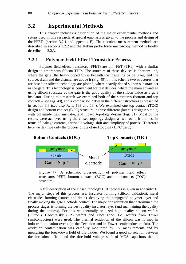
80 Chapter 3- Experiments in Polymer Field Effect Transistors
3.2 Experimental Methods This chapter includes a description of the major experimental methods and
setups used in this research. A special emphasis is given to the process and design of the PFETs (section 3.2.1 and appendix E). The electrical measurement methods are described in sections 3.2.2 and the Kelvin probe force microscopy method is briefly described in 3.2.3.
3.2.1 Polymer Field Effect Transistor Process Polymer field effect transistors (PFET) are thin FET (TFT), with a similar
design to amorphous Silicon TFTs. The structure of these devices is “bottom up”, where the gate (the heavy doped Si) is beneath the insulating oxide layer, and the source, drain and the channel are above it (Fig. 49). In this scheme two structures that are based on silicon technology are plotted, where heavily doped silicon substrate act as the gate. This technology is convenient for test devices, where the main advantage using silicon substrate as the gate is the good quality of the silicon oxide as a gate insulator. During this research we examined both of the structures (bottom and top contacts – see Fig. 49), and a comparison between the different structures is presented in section 3.3 (see also Refs. 133 and 134). We examined one top contact (TOC) design and bottom contact (BOC) structure in three different (lateral) designs: simple, with polyimide field insulator, and closed topology design (Fig. 51). Most of the results were achieved using the closed topology design, as we found it the best in terms of leakage currents, threshold voltage shift and simplicity of process. Therefore here we describe only the process of the closed topology BOC design.
Top Contacts (TOC)Bottom Contacts (BOC)
polymer
Gate – Si p++
Oxide MetalelectrodeGate – Si p++
Oxidepolymer
Top Contacts (TOC)Bottom Contacts (BOC)
polymer
Gate – Si p++
Oxide MetalelectrodeGate – Si p++
Oxidepolymer
Figure 49: A schematic cross-section of polymer field effect transistors PFET, bottom contacts (BOC) and top contacts (TOC) structure.
A full description of the closed topology BOC process is given in appendix E. The major steps of this process are: Insulator forming (silicon oxidation), metal electrodes forming (source and drain), deploying the conjugated polymer layer and finally making the gate electrode contact. The major consideration that determined the process stages is forming the best quality insulator layer (and maintaining the quality during the process). For this we thermally oxidized high quality silicon wafers (Siltronix Czochralsky (CZ) wafers and Float zone (FZ) wafers from Tower semiconductors) were used. The thermal oxidation of the silicon was formed in industrial oxidation ovens (in the Technion and in Tower semiconductors fub). The oxidation contamination was carefully monitored by CV measurements and by measuring the breakdown field of the oxides. We found a good correlation between the breakdown field and the threshold voltage shift of MOS capacitors that is

Chapter 3- Experiments in Polymer Field Effect Transistors 81
determined by the concentration of mobile charges in the oxides. And the breakdown field of best quality oxides we used was higher than . We found that applying a lift-off method while forming the electrodes, or exposing the gate oxide to photo-resist deteriorated the oxide quality in terms of breakdown field in MOS capacitor, concentration of mobile charges in the oxide, and as a result, threshold voltage shift. Therefore we evaporated the metal electrodes immediately after the oxidation and formed the gate by etching the electrodes. As the metal layer we used was Ti:Au the titanium improved the adhesion to the oxide and acted as a protection layer while etching the gold in a potassium ions rich solution. The titanium etch was found not to deteriorate the oxide quality. Following the electrode evaporation and pattering, the conjugated polymer layer was deployed by a spin-coating followed by a thermal treatment. The final stage of the transistor fabrication was forming "back contact" to the silicon substrate, namely a contact to the gate that is common to all transistors on a chip (typically with silver-paint as the metal).
710 [V/cm]
The conjugated polymer layer was formed by a spin-coating followed by a thermal treatment. The polymer that was used in most of the results described here is MEH-PPV (poly-[2-methoxy-5-(2 '-ethyl-hexiloxy)-p-phenylenevinylene]) (American dye source inc. - ADS100RE) with a molecular weight of 100,000. We used dehydrated toluene solution (typically MEH-PPV:toluene 10 mg:1 ml, 10min@90oC). The solution and the following steps were formed in a glove box (oxygen and water vapor at lower concentrations than 2 ppm) or in a sealed bottle. The MEH-PPV toluene solution was spin-coated on the silicon substrate (typically 80 sec@1400 rpm), followed by thermal treatment above the glass transition that we measured by DSC (differential scanning calorimetry) (typically 2 h@90oC with slow ramp up and ramp down temperature rates). The process conditions varied slightly where different molecular weights or different polymers were used.
3.2.2 Electrical Characteristics – DC and Time Resolved Measurements
DC characteristics and time resolved measurements of the PFETs, at longer times than 300 mSec, were done using semiconductor parameter analyzer (SPA) HP4155C of Agilent technologies, in the glove box. Temperature dependent measurements were carried out in a vacuum chamber where with a Joule-Thomson cooling (MMR technologies inc.). Time resolved measurements at the time range between nano-seconds and seconds was carried out by a set up described in Figure 50. The source drain bias remained constant during the measurement by a power supply unit (Yokogawa 7651), and the gate voltage was switched by a pulse generator (Agilent 6614C). The current in the transistor was measured by a scope (Tektronix 3012) on a load resistor, that was changed according the time interval of the measurement (see section 3.3). Additional pulse generator (Oor-x 311) was used to reduce the pulse rate to 1 Hz.

82 Chapter 3- Experiments in Polymer Field Effect Transistors
R
OOR-X 311
Agilent 6614C
Yokogawa7651
Tektronix 3052
PFET
RR
OOR-X 311
Agilent 6614C
Yokogawa7651
Tektronix 3052
PFET Figure 50: Time resolved measurement setup for the short time scale (1 nSec-0.5 Sec).
3.2.3 Atomic Force Microscope in Kelvin Probe mode High-resolution potential distribution across the PFETs channel was measured
by Kelvin probe force microscopy – KPFM110,135 (Autoprobe CP - Veeco Inc.- with Kelvin probe homemade electronics136). In this method the contact potential difference (CPD) between the tip of the microscope and the surface is measured (with energy resolution of several meV). The high spatial resolution (tens of nanometers) is achieved by the use of atomic force microscope (AFM) tip as a Kelvin probe. The KPFM apparatus was placed inside a glove box with nitrogen atmosphere (with water and oxygen concentrations of <2ppm) in order to decrease the thickness of the water layer absorbed to the polymer that leads to potential screening137, and to decrease the tip-sample distance in order to get better potential and spatial resolution. In addition, the relative low oxygen partial pressure and the dark conditions kept during the experiments (that are similar to the process glove box conditions), minimized light induced oxidation of the polymer.
Topography and CPD were measured simultaneously in a non-contact mode. AFM and KP parameters were optimized to achieve tracking of local signal changes in the nanometer scale and to avoid topography-CPD crosstalk. The sample-tip distance was set as the minimal distance (20 nm) in which the tip-sample (mechanic and electrostatic) interaction did not affect topography and CPD measurements. As the tip-sample distance increases the CPD signal decreases138, however for a given tip-sample distance the measured surface potential is linearly proportional to the ‘real’ surface potential. We calibrate the proportional coefficient for a constant tip-sample distance by measuring the CPD over the polymer layer above the gold electrode. Explicitly, for the above-mentioned we found that the CPD changed linearly with the gold potential on a wide bias range of the contact with a linear coefficient of
. 0.60 0.05±Topography and CPD images were measured on bare transistor substrates
(without polymer layer) to ensure that no residual of fabrication related materials were left as aggregates on the gold contacts, on the SiO2 region and especially on their

Chapter 3- Experiments in Polymer Field Effect Transistors 83
interfaces. Transistor substrate were produced with relatively thin metal layers (50nm) in order to minimize the CPD broadening effect due to tip-sample electrostatic interaction (this effect is more pronounced by any topographic corrugation). The measured regions were selected to be free from topographically/electrostatically detected local contaminations in the polymer layer, and all the presented lines-scene are 5 averaged lines-scene. For measurements of sample under bias we used a semiconductor parameter analyzer (SPA) HP4155C to conduct current to voltage measurements and as a voltage source. The current was measured at adjacent time to the measurement, at the same bias conditions.

84 Chapter 3- Experiments in Polymer Field Effect Transistors
Results and Discussion
3.3 Structural Parasitic Effects in Polymer FET In this research we concentrated on test devices for mobility, namely on thin
film polymer thin film field effect transistors based on silicon substrate. As demonstrated below, in these devices there two dominating parasitic phenomena; threshold shift which mainly originates from moving charges in the insulating layer, and residual leakage current originated by the parasitic capacitance-resistance. The first problem was solved by a careful process with a tight control on mobile charges in the silicon oxide (see section 3.2.1). The second problem, namely the parasitic charging current, was solved by device design. In this section we describe the different designs we examined and time resolved measurements that were the primary experimental tool to validate the relation between the design and the electrical behavior of the devices, namely the equivalent circuit that approximates the FET behavior. One simplified assumption that accompanies us in the design stage described in this section is a constant mobility that is independent on the applied field and the charge concentration. We shall demonstrate in the next sections that this assumption is incorrect. Nevertheless, we show that most of the PFET characteristics can be derived using the high concentration mobility single value, derived from the saturation current at high gate voltage.
We examined two different structures; top contact (TOC) and bottom contact (BOC)133 (Fig. 49). The TOC PFETs were fabricated by evaporating Au contacts through an evaporation mask. Although we used LASER cutting to produce the mask, the dimensions of the mask determined that the channel in this structure is very long ( 25 [ ]mµ≥ ). Another disadvantage that is inherent to this process is the large area of the contacts that result in a significant decrease of the device yield. Moreover, as we shall demonstrate below this structure suffers from a high charging current with a very large decay time, namely the measured currents in this device do not stabilize even after several seconds. We note that the TOC may exhibit one advantage over BOC: As the emitting area of the source is higher, we expect that the source-channel and drain- channel serial resistance to be lower in this structure. Therefore this design may be a better choice when the serial electrode-channel resistance is a limiting parameter; namely, when the organic semiconductor exhibits high mobility and the metal-polymer Schottky barrier is relatively high. Nevertheless, due to the disadvantages described above we concentrated on the bottom contact structure. In figure 51 three designs that we examined are plotted: Simple, with polyimide field oxide and with a closed topology. The last two designs were determined to prevent leakage charging current to the periphery of the active area (as described below): in the field insulator design we surrounded the active channel area (brown "snake" in Fig. 51.b.) with a thick insulator (polyimide) to decrease the capacitance of the periphery of the active area to the gate (the silicon substrate). Although this step almost eliminated the charging current (Fig. 52, Fig. 53 and see also Ref. 133), we found that we could not achieve clean channels in this procedure (although that the removal of the polyimide was prior to the lithography and etch of the active area). Therefore we designed PFET that eliminated the charging current of one of the electrodes, and had an additional benefit of simplicity in production and a clean channel; namely, closed topology design (Fig. 51.c). In this design one of the electrodes is fully surrounded by the other

Chapter 3- Experiments in Polymer Field Effect Transistors 85
electrode. Through that we eliminated the charging current of the interior electrode that can act as the source or the drain according the applied bias.
(a)
(b)
(c)
Figure 51: Three designs of bottom contact structure: Simple comb design - a detail from the original design (a). The polyimide-field oxide – photograph of the active area prior to polymer deposition (gold – yellow, silicon oxide – brown, polyimide thick layer - green) (b). The closed topology design – a schematic plot (c).
-50
-40
-30
-20
-10
0
10 -20-15-10-50
VG=-18VVG=-16V
VG=-14V
VG=-12V
Cur
rent
(nA
)
VDS (V)
VG=-8V
VDS =-2.5V
-20-15-10-50
-40
-30
-20
-10
0
VG=-10V
VG=-8V
VG=-6V
VG=-4V
VDS (V)
Cur
rent
(nA
) (a) (b)-50
-40
-30
-20
-10
0
10 -20-15-10-50
VG=-18VVG=-16V
VG=-14V
VG=-12V
Cur
rent
(nA
)
VDS (V)
VG=-8V
VDS =-2.5V
-50
-40
-30
-20
-10
0
10 -20-15-10-50
VG=-18VVG=-16V
VG=-14V
VG=-12V
Cur
rent
(nA
)
VDS (V)
VG=-8V
VDS =-2.5V
-20-15-10-50
-40
-30
-20
-10
0
VG=-10V
VG=-8V
VG=-6V
VG=-4V
VDS (V)
Cur
rent
(nA
) (a)
-20-15-10-50
-40
-30
-20
-10
0
VG=-10V
VG=-8V
VG=-6V
VG=-4V
VDS (V)
Cur
rent
(nA
) (a) (b)
Figure 52: Measured drain current for BOC with polyimide field oxide (a) and TOC (b) structures. The channel lengths were 40 [ ]mµ m and 10 [ ]mµ respectively133 (PFETs A and B in appendix G).
Figure 53: Measured drain current as a function of time after applying a gate bias for top contact (TOC) and bottom contact (BOC) structures133 (PFETs A and B in appendix G).

86 Chapter 3- Experiments in Polymer Field Effect Transistors
The origin of the charging currents in the test PFETs is the high capacitance between the periphery of the active area of the transistor and the gate, i.e. the silicon substrate. For instance, an equivalent circuit of the TOC is plotted in figure 54. Beside the channel charging that is intrinsic to FETs, in this structure the area beneath the contacts (green) and the area around the transistor (blue) is charged while switching the gate from "off" to "on" (i.e. from |VG|<|VT| to |VG|>|VT|). While the charging of the capacitor beneath the contacts is relatively fast, (assuming low contact resistance where compared to the channel resistance), the charging of the periphery is very slow (several seconds in our TOC transistors, see Fig. 53), and does not stabilize during a normal "DC" measurement. The long stabilization time result in a strong deviation of the PFET "DC" characteristics from ideal FET characteristics (see Fig. 52.a). This effect is almost completely eliminated by the field insulator BOC transistor s (Fig. 52.b), and fully eliminated in the closed topology BOC design. The reason for this is clear while examining the equivalent circuit of the BOC closed topology structure (Fig. 55), as in this structure the parasitic capacitances of the interior electrode is eliminated completely (we ignore metal-silicon capacitance as the resistance of the Au metal line is much lower than the polymer).
A visualization of the charging of the charging process of TOC device is given in figure 56. The charge concentration distribution in space at different times was obtained from a numerical calculation of 2D Poisson – continuity equations, by a method described elsewhere134*. We note that the mobility was assumed to be constant in this calculation, in order to isolate device related phenomena. The charging process can be divide into three stages: fast charging of the area beneath the contact (b), the intermediate time scale charging of the channel (c and d) and the long charging process of the periphery (d). The long charging of the periphery results in distortion of the "DC" characteristics: the additional charging currents (see currents in the equivalent circuit, Fig. 54) and a potential drop between the electrode and the area beneath it (Fig. 57 and Ref. 134). We can describe the TOC structure as a combination of three devices: Electrode diode, effective transistor distributed resistors-capacitors line, and resistors-capacitors distributed line of the periphery. When the electrode diode resistance is higher than the transistor resistance, as expected at low drain-source bias, the partition between the channel current and the periphery current results in a potential drop between the source/drain and the "virtual source/drain" (the areas beneath the electrode), and therefore a distorted FET "DC" current characteristics.
We summarize, that the top contact structure exhibit the following disadvantages: 1) High parasitic capacitance beneath the source and the drain and around the device, that results in very long charging before stabilization. 2) Long channels that are inherent to the evaporation mask dimensions. 3) Inability to produce cyclic topology of the transistor (in one evaporation), namely a transistor with one electrode (drain) that fully surrounds the other electrode (source). 4) Low yield of operating transistors. Due to these disadvantages we chose the closed topology BOC structure as the primary test device. In the next section we present channel charging measurements of these devices.
* All of the simulations presented here were obtained by N. Tessler.
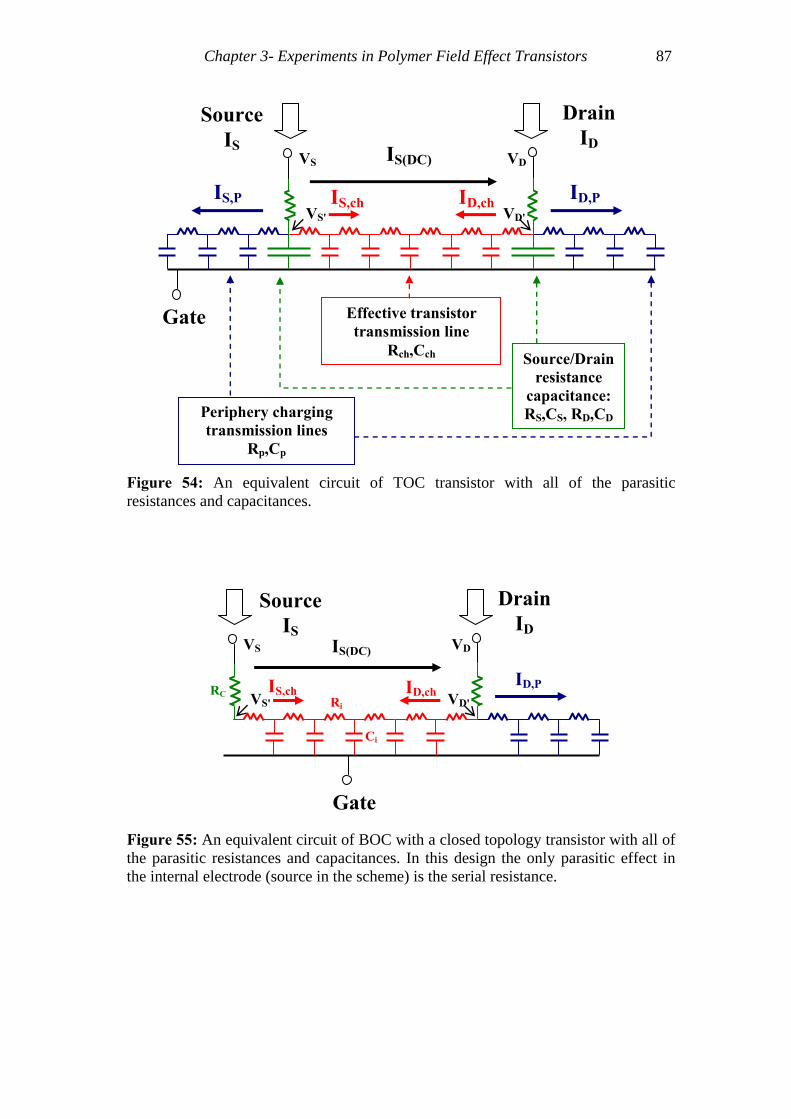
Chapter 3- Experiments in Polymer Field Effect Transistors 87
SourceIS
DrainID
Gate
VS
VS'
VD
VD'
IS(DC)
IS,P ID,P ID,ch IS,ch
Periphery charging transmission lines
Rp,Cp
Effective transistor transmission line
Rch,Cch Source/Drain resistance
capacitance:RS,CS, RD,CD
Figure 54: An equivalent circuit of TOC transistor with all of the parasitic resistances and capacitances.
SourceIS
DrainID
Gate
VS
VS'
VD
VD'
IS(DC)
ID,P ID,ch IS,ch Ri
Ci
RC
Figure 55: An equivalent circuit of BOC with a closed topology transistor with all of the parasitic resistances and capacitances. In this design the only parasitic effect in the internal electrode (source in the scheme) is the serial resistance.

88 Chapter 3- Experiments in Polymer Field Effect Transistors
Ch
arge
Den
sity
(1018
cm-3
)
Length (µm)Depth (µm)
Drain Source
t=0(a)
Ch
arge
Den
sity
(1018
cm-3
)
Length (µm)Depth (µm)
Drain Source
t=0(a)
Ch
arge
Den
sity
(1018
cm-3
)
Length (µm)Depth (µm)
Short t
DrainSource
(b)
Ch
arge
Den
sity
(1018
cm-3
)
Length (µm)Depth (µm)
Short t
DrainSource
(b)
Ch
arge
Den
sity
(1018
cm-3
)
Length (µm)Depth (µm)
Long t
Drain
Source
(c)
Ch
arge
Den
sity
(1018
cm-3
)
Length (µm)Depth (µm)
Ch
arge
Den
sity
(1018
cm-3
)
Length (µm)Depth (µm)
Long t
Drain
Source
(c)
-1
0
1
2
3
4
5
6
7
-5 0 5 10
Length [µm]
Ch
arge
Den
sity
[10
18cm
-3]
(d)
0.1 sµ
1 sµ3 sµ
4.5 sµ
6 sµ
-1
0
1
2
3
4
5
6
7
-5 0 5 10
Length [µm]
Ch
arge
Den
sity
[10
18cm
-3]
(d)
0.1 sµ
1 sµ3 sµ
4.5 sµ
6 sµ
Figure 56: 2D calculation (Poisson + continuity equations) results of TOC transistor, at different times after gate opening (0 sec (a), 140 nsec (b), and 4.5 secµ (c)). Calculated charge density at different times after VG was switched from 0 to -5 V (VS=0 V, VD=-3 V). Charge density at the polymer-insulator interface134.
D
S
S’
D’
Pote
ntia
l (V
)
Length (µm)
Depth (µm)
(a)
D
S
S’
D’
Pote
ntia
l (V
)
Length (µm)
Depth (µm)
D
S
S’
D’
Pote
ntia
l (V
)
Length (µm)
Depth (µm)
(a)
(b)
Figure 57: (a) Calculated 2D potential distribution for the TOC structure. The transistor active region has reached its steady state. (b) Schematic description of the potential distribution between the contacts for varying drain voltage (for illustration, a Schottky barrier was introduced at the contacts)134.

Chapter 3- Experiments in Polymer Field Effect Transistors 89
3.4 Channel charge build-up In this section we describe the intrinsic channel charging of the PFET. We
isolated the intrinsic channel charge buildup from the residual parasitic charging processes by measuring the current on the interior electrode of BOC closed topology PFET. As demonstrated in figure 55 the only parasitic effect that influences the measured current on the interior electrode in this design is the serial resistance of the metal-polymer interfaces. As these interfaces (at both electrodes) behave as diodes, we expect the contact conductance to be highly non-linear and that the current at low drain-source biases to decrease (Fig. 58). In some of the transistors, where the metal-polymer semiconductor barrier ( bφ ) was high, or when the metal-polymer was not completely clean we observed this phenomena (Fig. 58.b). Nevertheless, in several transistors the contact resistance was negligible, and we chose one of these devices to measure the channel buildup (Fig. 59). (all of the measurements were performed on the interior electrode of a closed topology BOC PFET; and therefore no peripheral charging was observed).
(a)
VDS
I S
Contact "diode" Channel:
Ideal transistor
Real transistor
-8-6-4-200
10
20
30
40
50
60
70
Vds [V]
Is [n
A]
(b)
Contact Resistance φb~0.6 V
VG=0-(-20) [V]
Figure 58: The influence of electrode metal/polymer diodes (contact resistance). A schematic description (a), and a real MEH-PPV transistor with Au electrodes measurements (b). (PFET C in appendix G)
-20-15-10-500
100
200
300
400
500
600
700
Vds [V]
Is [n
A]
VG -20 V
-18 V
-16 V
-14 V
-12 V
-10 V
-8 V -6 V -4 V
µsat=2x10⁻⁴
[cm2/Vsec]
(a)
-20-15-10-500
100
200
300
400
500
Vgs [V]
Is [A
]
-20-15-10-50
10-2
100
102
Vgs [V]
Is [A
]
VD
-6 V
-8 V
-7 V
-5 V -4 V
-3 V
-2 V
-1 V
-0.5 V
(b)
Figure 59: Conductance (a) and transconductance (b) characteristics of PFET with a negligible contact resistance. (PFET D in appendix G)

90 Chapter 3- Experiments in Polymer Field Effect Transistors
In figure 60 plotted time resolved current, after the gate voltage was switched from 0 V to -8, where the drain source bias was kept constant. The PFET is made of MEH-PPV with Au contacts (for more details see subtitle of Fig. 59). The experimental setup for the time resolved characteristics is described in section 3.2.2. The load resistor was changed from 100 Ω to 10 kΩ in order to decrease the RC current of the load resistor and gate (and circuit) capacitance beyond the channel current (e.g. see end of RC current decay in 1 kΩ curve at [ ]52 10 sect −< ⋅ ), and to achieve good signal to noise ratio in all time scale. (The attenuations at the very short times are due to reflections of the measurement circuit lines: as the measurement was in the glove box and the electrical equipment out of it.). The source current decreases according a power law over a large time range (approximately three decades), till it reaches the DC current value. At this time (ton) the channel is switched to open, and the drain current increases from very small, opposite in sign current, to it DC value. The switching time exhibit a scaling low with the squared channel length (insert in Fig. 60). As the current before the switching time is the channel charging current this can be simply explained: The total charge of the channel is proportional to channel length. On the other hand the momentary electric field, and therefore the current are proportional to the inverse channel length (assuming constant mobility). Therefore the switch-on time (as well as the time to reach any intermediate situation of charge distribution, where the distance is normalized to the channel length) is proportional to the squared channel length ( 2/ ~ /Q J Q E L= ).
10-6 10-5 10-4 10-3 10-210-8
10-7
10-6
10-5
t [sec]
I [A
]
0 5 9 170
0.03
0.06
Lchannel [µm]
t on1/2 [s
ec1/
2 ]
Is 100 ΩIs 1 kΩIs 10 kΩId 10 kΩ
ton
Figure 60: Measured source (blue) and drain (red) currents of PFET (as described in Fig. 59 title) after switching the gate voltage from 0 V to -8 V where the drain voltage was kept at constant bias (VDS=-8 V). The switching time (ton) is the time that drain current reaches its DC value, the channel charging is completed and the source and the drain currents are equal. The scaling low of the switching time with the squared channel length is presented in the insert. (PFET D in appendix G)

Chapter 3- Experiments in Polymer Field Effect Transistors 91
The power-law observed decay of the current is significantly different than the exponential decay observed at relatively long time scale, and small signal in Ref. 139. Such an exponential decay was observed in our measurement only at times adjacent to the switch-on time and are attributed here to extrinsic RC effects. On the other hand the experimental observation of the power low dependence of the current on time and the scaling law of the switching time with channel length confirm the two dimensional Poisson-continuity equations numerical results (not presented here). Nevertheless, the two dimensional numerical solution of these equations is complex and time consuming. Here we present a simpler approach to describe the PFET transient behavior at moderate and high biases, where the mobility can be regard as constant with charge concentration and applied field117,140.
Our approach relies on distributed line (transmission line) presentation of the channel (see Fig. 55). In this approach the channel is present by a series of resistors and capacitors (Ri and Ci, respectively). This presentation is convenient to apply in VLSI numerical simulators, as the transistor is replaced by a simple equivalent circuit composed of linear elements. We note that a continuum approach, similar to ours was presented in Ref. 139. However it was fully solved only for limited conditions, namely where variable separation can be applied*. This assumption is applicable only for small signal (small change between the voltage before and after switching), and for this reason it is applicable only for the end of the charging (close to the switch-on time), when the current decays exponentially in time. As demonstrated by the time resolved measurements, and as the full solution demonstrates (see Fig. 57.d. and Fig. 61), this assumption is not valid for short times, particularly for large signals. Explicitly, we observed and calculated currents that vary in time according a power-law, and not according an exponential decay. Therefore, we developed a general approach for the solution of the current and potential dependence on time.
The solution is based on a distributed line of capacitors and resistors of the PFET channel. Ri are the serial resistance associated with the current that flows through, and fill up, the channel. The resistance, Ri, is derived from the conductivity as:
1*i
L LRA q p d W q pπ
1µ µ
∆ ∆= = (3.4.1)
where ∆L is the distance separating two elements. The charge density p is determined by the voltage that drops across the capacitors next to Ri:
1 1
1* *
2 2* *
ii i i i
ins ins
L LRV V V Vd W WC L W C
qqd L W
π
π
µµ
1+ +
∆ ∆= =
+∆
∆
+ (3.4.2)
To solve the equivalent distributed line of the channel we require defining the boundary conditions:
1 1
0
; ;1, 1 0
S n D
i t
V V V Vfor i n V
+
=
= =⎧⎪⎨ ≠ + =⎪⎩
(3.4.3)
* To be precise, a slightly different condition is assumed there, namely ( ),V x t XT const= + .

92 Chapter 3- Experiments in Polymer Field Effect Transistors
and for the dynamics of the system we rely of the capacitor characteristics i
idVI cdt
⎛ =⎜⎝ ⎠
⎞⎟ and on Kirchof law
1i ii R RI I I−
= − :
1
1
1i i i i
ins i i
dV V V V Vdt C W L R R
−
−
⎛ ⎞− −= −⎜⋅ ⋅ ∆ ⎝ ⎠
1i+⎟ (3.4.4)
As we assumed that µ is field and density independent we arrive at an expression similar to the continuous form139:
( 2 2 212 2
2i
i i idV
V V Vdt L
µ−= − + )1+∆
(3.4.5)
and finally the transient currents are:
2
1
( )( )
( )( )
SS
D nD
n
V V tI t
RV V t
I tR
−⎧ =⎪⎪⎨ −⎪ =⎪⎩
(3.4.6)
The above equations suggest that the transistor switch on characteristics are rather universal and only depend on the channel length, the material mobility, and the insulator capacitance (where the last only determines the absolute value of the current, but not the time dependence). In figure 61 the charge concentration distribution in the channel (that is linearly dependent on the potential distribution) is plotted for different time after voltage switching. It is clear that at the short time range a solution that relies on variable separation (namely, ( ),V x t XT const= + ) cannot be applied. Two different situations can be identified: (a) Gate switching bias that is in the saturation
0 2 4 6 8 10 12 14 160
1
2
3
4
5
6
7
8
Xchannel [µm]
Cha
nnel
cha
rge
[V*C
ox] (a)
0 2 4 6 8 10 12 14 160
2
4
6
8
10
12
14
16
Xchannel [µm]
Cha
nnel
cha
rge
[VC
ox] (b)
Figure 61: Transmission line method (TLM) Calculated surface charge in the FET channel at different elapsed times after operating gate bias for: (a) low drain voltage ( , 8 [V], 0GS T DS GS DS TV V V V V V− ≤ = = − = ), and (b) high gate voltage
( , GS T DSV V V− > ). Where the gate voltage is low (a) the charging is only from the source, and there is one exponent (one slope) in the current-time dependence. Where the gate voltage is high (b) the charging is from the source and the drain, and when the charge frontiers from both sides meet (brown curve) the current exponent changes to another value. The colors at both graphs present the same elapsed time after switching the gate voltage.
16 [V], 8 [V], 0GS DS TV V= − = − =V

Chapter 3- Experiments in Polymer Field Effect Transistors 93
range ( GS T DSV V V− ≤ ), and (b) gate switching voltage that is in the linear range
( GS T DSV V V− > ). In the first situation (Fig. 61.a.) the charging is only from the source and the drain charging is negligible. This result in one slope (nominator) in the log-log current-time curve. On the other hand, when the switching is to the triode (linear) range of the transistor (Fig. 61.b. and see also Poisson-continuity equations 2D solution in Fig. 57.d.), the charging is both from the source and the drain. When the charge "frontiers", that advance from the source and the drain, meet, the source current decays much faster toward the DC source current. Explicitly, the slope of the log-log current-time curve changes and the curve becomes steeper. This observation (measurement and calculation result) can be seen in figure 62. We note that all of the calculated curves use the same parameters: [ ]4 21.4 10 [cm / sec], 3.6 VTV Vµ −= ⋅ = −
and (that is originated from a slight bias difference at the load resistor due grounding potential difference). We note that the threshold voltage is similar to that observed in the DC measurements, however there is a slight change in the mobility between the DC and the charging values ( ).
89 10 [A]noiseI −= ⋅
4 22 10 [cm / sec]DC Vµ −= ⋅Finally, we must ask ourselves how is that the distributed line method and the
two dimensional Poisson-continuity equations solutions describe the result so well, although they rely on a constant mobility approximation? We demonstrated theoretically (chapter 2) and experimentally (see next sections) that the mobility in this material is strongly charge density dependent. As the channel is charged from an
10-4
10-3
10-7
10-6
t [sec]
-2 V-3.7 V-5.3 V-6.8 V-7.5 V-8.3 V-9 V-10 V-12 V-13.6 V-15 V-16.6 V-18 V-20.8 V
Is [A
]
VG
Figure 62: Experimental and transmission line simulation results (colored and dashed lines, respectively) of PFET charging current for different gate voltages (VD=-8 [V]). All of the simulation are with the same parameters:
. At low currents the charging deviates from the simplistic simulation due to the decrease of the mobility at low concentrations and the residual charging current (due to the load resistor and gate capacitance). The one exponent and two exponent charging modes enable to determine the threshold voltage. (PFET D in appendix G)
4 2 83.6 [V], 1.4 10 [cm / sec], and 9 10 [A]T nV V Iµ − −= − = ⋅ = ⋅oise
94 Chapter 3- Experiments in Polymer Field Effect Transistors
empty condition to high concentration condition, one may expect that the transient curves will deviate from the universal, constant mobility shape. Nevertheless, except the low gate bias curves that deviated significantly from the constant mobility approximation, the other curves were successfully described over a wide range of biases and time by this model. We assume that the constant mobility is kept by the three parameters that drive the mobility toward its maximal value: out of equilibrium condition (at the very short time after gate switching), high voltage (at the charging frontier) and an increase of charge concentration. According the Hopping (Miller-Abrahams) model there is a maximum mobility value that is related to a maximum amount of sites that were lowered beyond the initial site energy. This value can be reached by all of the mentioned above parameters, but the mobility is limited not to cross this maximum mobility value. A mobility that is close to this value is the critical mobility in all of the charging process, as long as the final gate bias is high (high final concentration at the gate). Deviations from the "universal behavior" are observed when the gate bias is small, and the mobility is no longer constant, as can be seen in the lower curves in figure 62. On the other hand, there may be several reasons for deviations in the low gate bias curves besides the non linearity of the mobility on charge concentration, as the "tail" of the load resistor-gate RC current decay, longer time to reach equilibrium conditions. Therefore to quantify the non-linearity of the transport in charge concentration we approached a different direction, namely close inspection of the DC PFET characteristics, as introduced in the next section.

Chapter 3- Experiments in Polymer Field Effect Transistors 95
3.5 Mobility Extraction from Transfer Characteristics
In this section we introduce an accurate method to extract the mobility dependence upon charge concentration in PFETs. The aim of this section is to introduce a new method to analyze transconductance characteristics of FET, namely polynomial expansion method. The examination of the primary forecasts of the mobility calculation introduced in chapter 2 is introduced in next sections. The polynomial expansion method that enable extracting charge carrier dependence of mobility accurately from transconductance characteristics of FETs was developed in collaboration with O. Katz (mostly at afternoons) and we follow in this section Ref. 141. A farther expansion of this method that enables analyzing charge concentration and field dependent mobility, given in this reference, is not presented here.
3.5.1 Mobility extraction methods in field effect transistors
Charge carrier transport behavior has been studied in PFET channels (see section 1.3.4 and Refs. 5,104-106,108,124,142-144) as well as a variety of other semiconductors (e.g. silicon, and inorganic III-V 2D semiconductor system101,102), in order to examine non-linear effects of charge concentration semiconductors. Since the mobility is a strong non-linear function of charge concentration (and electric field) in these materials, conventional methods to analyze the transfer characteristics of the FET were found to be inaccurate (see discussion below), and a need for a new analysis method emerged.
The conventional method to determine the charge concentration dependent mobility in FET is based on the capacitance-conductance (CC) measurement (e.g. Refs. 100,101,145). In the CC method, the mobility is commonly extracted from the transistor current derivative with the gate voltage (gm), or from the transistor current directly. One important limitation of these methods stems from the requirement of a constant mobility across the channel. This requirement is not fulfilled when the mobility is highly non-linear. For the case in which the mobility depends on the lateral electric field (as expected in PFETs) the problem is even more cumbersome, and the FET current differential equation becomes non-linear. In order to avoid this difficulty, researchers have either linearized the current equation for a given drain voltage ( )DSV
and gate voltage ( )GSV values, assuming that the charge concentration is constant along the channel, or applied numerical methods to calculate the transistor current. In this section, we propose a new analytical method to extract the mobility, µ , and its dependence on surface charge concentration, sn , and electrical field, ε , from the FET transfer characteristics. We develop an expression to extract the mobility from the transfer characteristics for carrier concentration dependent mobility ( )snµ . We note that in Ref. 141 we expand the method to carrier concentration and lateral electric field dependent mobility ( ),snµ ε .
96 Chapter 3- Experiments in Polymer Field Effect Transistors
Before presenting the new method, we describe the commonly used formalisms to extract the carrier mobility in the transistor channel, and demonstrate the inherent inaccuracy of their results when the mobility is highly non-linear. The transistor current in the triode region for a constant mobility along the channel is given by:
( ) 212DS g GS T DS DS
WI C V V V VL
µ ⎡ ⎤= − −⎢ ⎥⎣ ⎦ (3.5.1)
where is the threshold voltage; W, L and CTV g are the channel width, length and the gate capacitance (per unit area), respectively. A common method to extract the mobility from the transfer characteristics is based on derivation of the transistor current with respect to the gate voltage (Eq. (3.5.1)).
mUT
g DS
g LC V W
µ = (3.5.2)
where the gm is the transconductance defined by: m DS Gg I V S≡ ∂ ∂ . In Eq. (3.5.2), namely the uniform mobility transconductance method (UT), the mobility derivative was neglected and a uniform mobility across the channel was assumed, (In the following, carrier mobility calculated with Eq. (3.5.2) will be denoted UTµ ). The proper calculation, that accounts for the derivative of the mobility, is:
12
mGS T DS
g DS GS
g L V V VC V W V
µµ ∂ ⎡ ⎤= − − −⎢ ⎥∂ ⎣ ⎦ (3.5.3)
Often, the second term cannot be neglected117, as the next example demonstrates. Let us consider a power law dependence of the mobility on the carrier concentration;
(as suggested in Ref.( ) ( ) ( )ns GS GSn V a V Vµ µ= = − T
7 for conjugated polymers). We
assume that DS GSV V V− T , so that the mobility is constant along the channel. Extraction of the mobility from Eq. (3.5.2) results in over estimation of the mobility, i.e ( )1UT nµ µ= + . Furthermore, if the mobility changes with carrier concentration or with lateral electric field, the commonly used assumption of a constant mobility along the channel is not valid unless the measurement is conducted under a relatively low applied DSV such that DS GSV V V− T . Measurements at such low DSV results in a low signal to noise ratio, reduces the accuracy of the result, and hence are limited to a very narrow range of ns. Therefore, it is clear that the mobility calculated from Eq. (3.5.2) is erroneous for strong non-linearity with charge concentration (even under the condition DS GSV V V− T ), while mobility extracted directly from Eq. (3.5.1) is erroneous for the spatially non-uniform case (i.e. when the source-drain voltage is not much smaller than the gate bias, DS GSV V V− T ).
3.5.2 Mobility extraction polynomial expansion formalism
Here we present a method to extract the mobility from the transistor transfer characteristics, namely the current-voltage curves where the charge carrier mobility depends on the charge concentration but not on the lateral electric field. We assume

Chapter 3- Experiments in Polymer Field Effect Transistors 97
that the gradual channel approximation is valid, and that the channel local voltage (voltage at lateral position ( )v x x along the channel conductive layer) is linear with
carrier surface (2D) concentration according to
( ) ( ) ( )s g GS Tn x C q V V v x= − −⎡ ⎤⎣ ⎦ (3.5.4)
where q is the electron charge and Cg is the surface gate capacitance. Since the lateral electric field can be written as, ( ) ( )dv x dx v xε ′= − = − , and the channel current is
constant along any point ( )x between source and drain, it can be written as,
( ) ( ) ( )DS s
dv xI Wqn x x
dxµ= (3.5.5)
where W is the channel width. We present the general dependence of µ on ns by a polynomial expansion of the local voltage, ( )v x ,
( ) ( ) ( )0
N ns n GS T
nx n x V V v xµ µ µ
=
= = − −⎡ ⎤ ⎡⎣ ⎦ ⎣∑ ⎤⎦ (3.5.6)
where nµ are the polynomial expansion (unknown) coefficients. The current in the triode region is calculated by inserting Eq. (3.5.6) into Eq. (3.5.6) and integrating from source to drain (the potential drop on the parasitic series resistances was neglected);
( ) 1
00
DSV N n
DS g n GS Tn
WI C V V vL
µ+
=
= −∑∫ dv− (3.5.7)
From the derivative of the current with respect to the gate voltage, we obtain the following expression for the transconductance at the triode region,
( ) ( )1
0
Nn
m g n GS T GD Ttrioden
Wg C V V V VL
µ +
=
1n+⎡ ⎤= − − −⎣ ⎦∑ (3.5.8)
GDV is the gate-to-drain voltage. Similarly, the transconductance at the saturation region can be calculated from Eq. (3.5.7) (where the integration limits are 0, VG-VT), results in;
( 1
0
Nn
m g n GSsaturationn
Wg C V VL
µ )T+
=
= ∑ − (3.5.9)
By fitting the derived function to the measured transconductance for a varying gate bias, the polynomial parameters nµ , and therefore the mobility dependence on the charge concentration can be calculated. Using the polynomial expansion the mobility dependence on charge 2D-concentration can be accurately extracted for a wide range of carrier concentration values, over the whole triode and saturation regions and without any limitation on the DSV value, in contrast to mobility extraction by the uniform mobility approximation (Eq. (3.5.1)),.

98 Chapter 3- Experiments in Polymer Field Effect Transistors
In the following we present examples in which the function ( )snµ is known, and we calculate the I-V and transfer characteristics of the device, using the polynomial expansion (PE) method (Eq. (3.5.8)). Explicitly, we determine the nµ coefficients by a polynomial fit of a realistic mobility model, and the current is calculated from Eq. (3.5.7) and (3.5.8). Now, we assume that the I-V characteristics are given, and for that we calculate back ( )snµ by the three different methods. In figure 63 we compare the PE method to the uniform mobility current approximation (UMC) i.e. current equation (Eq. (3.5.1)) and uniform transconductance (UT) (Eq. (3.5.2)) methods. By this example we will show the relative accuracy of these approximations. Our example is a power law dependence of the mobility at low charge concentration, that saturates to a constant high value at high concentrations. This dependence may describe the low mobility of charge carriers in conjugated polymers and other amorphous organic semi-conductors7,106,124,146. While the proposed method (PE) restores accurately the mobility value, the transconductance method (UT) over estimate the maximum mobility (and even predicts an artificial peak), and under estimate the minimum mobility (to negative mobility values). On the other hand, the mobility extracted directly from the current (the UMC method) is averaged over the channel, and therefore the changes are less pronounced in comparison to the original values. The difference between mobility values extracted from the current equation to these of our formalism, increases with DSV , while the two methods merge at the limit DS GSV V V− T , i.e. at high concentrations. Finally we note the polynomial expansion method, as well as all of the other method is highly sensitive to threshold voltage determination. In the next sections we demonstrate that determination of the exact threshold voltage is subtle when the mobility strongly depends on charge concentration, and demonstrate the application of the polynomial expansion method on measurements results of MEH-PPV PFETs.
5.0x10¹² 1.0x10¹³ 1.5x10¹³ 2.0x10¹³ 2.5x10130
1x10⁻⁵
2x10⁻⁵
3x10⁻⁵
4x10⁻⁵
5x10⁻⁵
6x10⁻⁵
7x10⁻⁵
2 4 6 8 100
50
100
I DS (
nA)
VGS (Volt)0
5
10
15
g m (n
S)
original µ UT UMC PE
Mob
ility
(cm
2 /Vs)
ns (cm-2)
Figure 63: Typical mobility dependence on charge concentration in conjugated polymers based FETs (full circle). The mobility is extracted by the conventional transconductance method (UT - dotted), the current equation method (UMC - dashed), and by the suggested polynomial expansion method (PE - solid). The insert shows the FET transfer characteristics.

Chapter 3- Experiments in Polymer Field Effect Transistors 99
3.5.3 Determination of the threshold voltage
The mobility extraction from the transfer characteristics by the PE (polynomial expansion) and the UMC (uniform mobility current approximation) methods relies on an accurate determination of the threshold voltage (VT). The common method to determine the threshold voltage is from the current in transfer characteristics where the voltage at which we measure current; namely, "switch-on voltage" (Vopen), is assumed to be the threshold voltage. However, it has been demonstrated that when the mobility is highly dependent on the charge concentration, a significant difference between the threshold voltage that resembles flat band condition, and the switch-on bias may occur105. We demonstrate the origin for this difference by plotting the calculated transconductance curve of three different PFETs (Fig. 64): Constant mobility (blue solid line), mobility that strongly depends on charge concentration (dotted green line), and lightly doped semiconductor, with constant mobility (dashed red line). In all of the calculated curves the threshold voltage is -1 V, and the high concentration mobility is the same. The concentration dependent mobility model (see insert in Fig. 64.b) is ( )tanh TV V αµ = − , that behaves
at low biases like a power law, and saturate at high biases to a constant high concentration mobility value. The doped material current was calculated according Ref. 147. Typically the threshold voltage is determined as the first voltage at which a measurable current flows (Von), where the current is plotted in a logarithmic scale (Fig. 64.a). In this simplistic method, the threshold assessment is determined by the sensitivity of the measurement equipment, particularly when the mobility increases with charge concentration, and the current slope near the threshold voltage is low. For instance, the switch-on voltage is different where the equipment sensitivity is 10-9 [a.u.] (bottom of the figure) or 10-8 [a.u.] (dotted black line). Another reason for an error in this method may be a small parasitic current (e.g. from un-intentional doping) that may be interpreted as a threshold voltage shift.
Another method is extrapolation of the high concentration curve (where the mobility is assumed to be constant) backward toward zero current (in the linear plot) and determination of the threshold voltage as:
int 2T DV V V S= − (3.5.10)
where Vint is the cross point between the interpolation line and the zero current line. This method overcomes the influence of small residual doping current, as the current with and without doping merge at the high gate voltage range. On the other hand, if the mobility did not saturate at the highest (absolute) gate bias, the slope of the current curve may be steeper that constant mobility slope, which result in overestimation of the absolute threshold voltage (e.g. the slope of the green curve at VG= -15 V). We note that a typical behavior of the mobility dependence on charge concentration has a turn point. Namely, the current slope increases and afterwards decreases in an S shape (see green curve in Fig. 64.b.). Without observation of this behavior the extrapolation method certainly lead to an error in VT. Nevertheless, an observation of the S shape curve does not insure that the mobility saturated at a constant value (Moreover, a slight shift of the threshold voltage during the measurement is often manifested as an S shape curve as well).

100 Chapter 3- Experiments in Polymer Field Effect Transistors
-20 -15 -10 -5 010-9
10-8
10-7
10-6
VGS [V]
Is [a
.u.]
µ(ns)dopingconst. µ
(a)
-20 -15 -10 -5 0
12345678 x 10-7
VGS [V]
Is [a
.u.]
µ(ns)dopingconst. µ
-10-1
-100
-101
10-8
10-5
|V-VT|
µ [c
m2 /V
sec]
(b)
Figure 64: Three calculated transconductance current characteristics of PFETs with constant threshold voltage (VT=-1 V, in all curves): constant mobility (blue, solid), concentration dependent mobility (grin, dotted) and constant mobility with a low doped bulk (red, dashed). The curves are plotted in logarithmic (a) and linear (b) scales. The mobility dependence of the dotted current curve is given in the insert in (b) in a log-log scale.
We conclude that determination of the threshold voltage from current characteristics is inaccurate, or relies on a detailed understanding of the mobility dependence on charge concentration, which typically is not known a priory. Here we suggest another new method (see also the transient method, section 3.4) based on KPFM measurement that does not rely on preliminary assumption of the transport mechanism or doping of the organic semiconductor. The method is based on the measurement of the surface potential by the KPFM. As long as the (absolute) gate bias is beyond the threshold voltage ( G TV V> ) the charge in the accumulation layer screens the gate potential and the increase of the surface potential is lower than the increase of the gate bias ( ). On the other hand, when the absolute gate bias is below the threshold voltage, (
G( potential)/ V 1Surface∆ ∆ <
G TV V≤ ), there are no mobile charges between the gate and the surface (polymer-air interface) and the slope of the surface potential versus gate bias curve is 1 ( G( potential)/ V 1Surface∆ ∆ = ). The cross point between the linear fit of these ranges yields the threshold voltage ( in this example). One may claim that this method is not valid for doped materials: In doped materials there are mobile charges at the flat band condition. In this case the slope at the sub-threshold is not expected to be constant, and not reach 1 value (as the mobile charges screens the gate potential). Nevertheless, the slope of the surface potential - gate bias curve is still expected to change (as long as the doping is not heavy), as the accumulation layer vanishes, and the gate change their spatial distribution at the sub-threshold region. On the other hand, in un-doped materials with very low mobility at low charge concentration a slight difference between the threshold voltage and the cross-section point as the low mobility cause the material to behave as an insulator.
1.75 0.15 [V]− ±

Chapter 3- Experiments in Polymer Field Effect Transistors 101
2 4 6 8 10 12-3.5
-3
-2.5
-2
-1.5
-1
-0.5
0
0.5
X [µm]
Hei
ght [
nm/1
00],
CP
D [V
] Vgs=-1 V
Vgs=-6 V
Topography
(a)
-5 -4.5 -4 -3.5 -3 -2.5 -2 -1.5 -1-0.3
-0.2
-0.1
0
0.1
0.2
0.3
0.4
VG [V]
Sur
face
pot
entia
l [V
]
VT
(b)
Screening(acumulation layer)
No screening
Figure 65: Kelvin probe and topography force microscopy scan results (a) of 9 [ ]mµ channel PFET operated at VDS=-4 [V] and VG between -6 and -1 [V]. (note that the applied bias is -4 [V] while the source-drain CPD difference is -2.5 [V]) as a result of the linear ratio between the CPD and the surface potential) The threshold is determined by plotting the CPD near the source (dashed line in (a)) versus the gate bias (b). At absolute gate bias that is lower than the threshold voltage, the surface potential increases linearly with gate bias, as there are no mobile charges to screen the gate potential. The slope change point denotes the threshold voltage ( in this example). (PFET E in appendix G)
1.75 0.15 [V]− ±

102 Chapter 3- Experiments in Polymer Field Effect Transistors
3.6 Charge transport characteristics of MEH-PPV
In the last experimental part, we examine the primary theoretical predictions that were presented in chapter 2, in one material system, (namely, MEH-PPV) by applying the measurement and analysis methods introduced in the former sections on MEH-PPV FETs. We demonstrate that there are two typical different behaviors of charge transport at the low concentration range. We evaluate the charge carrier DOS as extracted from the mobility measurements. Finally, we examine the effect of morphology and demonstrate that there is single high concentration activation energy for this material.
3.6.1 Mobility dependence on charge concentration and charge carrier DOS in MEH-PPV
In the former sections we established a new method (the polynomial expansion method) to extract accurately the mobility dependence on charge concentration from transfer characteristics of PFETs, and we demonstrated how to determine the threshold voltage from KPFM measurements. In this section we explore the mobility dependence on charge concentration in MEH-PPV PFETs, by applying these methods. We open the section by examining the correspondence between the theoretical results of the different extraction methods to real measurements. In Fig. 66.a the transfer characteristics (IS vs. VG) of MEH-PPV (ADS 100RE) PFET are showed. As this transistor was not examined by KPFM, we rely on other methods to determine the threshold voltage. A common method to evaluate the threshold voltage is by backward extrapolation linear region (see former section). Explicitly, we assume that the mobility is constant at the high bias, linear range, and backward extrapolate the transfer curve of the constant mobility (dotted line in Fig. 66.a). The extrapolated "high-current" threshold voltage is the cross-section between the calculated constant mobility curve and the independent axis (see insert in Fig. 66.a). We assume that the high concentration mobility is always higher than (or equal to) the mobility at lower concentrations, and that the threshold voltage does not shift during the measurement. As we shall demonstrate below, the later assumption is not valid in PFETs as the high current and low current effective threshold voltages do not unite*. In this example, the back extrapolation method results in non-realistic difference between the turn-on voltage and the threshold voltage. In other examples this method leads to inconsistency. For instance, a typical observation in MEH-PPV PFETs is that the switch-on voltage is lower than the extrapolated threshold voltage ( - namely, V
,on T extV V>
on is on the left hand side of VT,ext. e.g. Fig. 66.a). In these transistors the current at the sub-extrapolated-threshold voltage range do not follow doping current equations147, namely in our observation it increases exponentially with gate bias (Fig. 67.a and Fig. 68.a). Therefore we assume it does not originate from a parallel
* The threshold voltage shift that is described here is intrinsic to the conjugated polymer, and appears at transistors with current characteristics that do not vary with time. We have carefully excluded threshold voltage shift that is related to existence of mobile charges in the oxide (or similar parasitic effects).

Chapter 3- Experiments in Polymer Field Effect Transistors 103
conductance in the polymer bulk. Under this assumption, the extrapolated threshold bias (VT,ext) cannot be the real threshold voltage. In order to calculate the mobility (Fig. 66.b) we replaced the non-realistic extrapolated "high-current" threshold voltage (VT,ext) with a more realistic value of (-1.6 [V]) and inserted it into the different mobility extraction methods, introduced in section 3.5.2. The result is similar to the theoretical calculation (Fig. 64). Namely, the transconductance method (UT) is clearly overestimating the mobility and results in an artificial peak, and the uniform current approximation (UMC) underestimate the mobility where compared to the polynomial expansion (PE) method. More reliable method to determine the threshold voltage is demonstrated in Fig. 67.b. In this example we calculated the mobility by PE and UMC methods from several source-drain biases transfer curves. The different mobility curves did not converge when we picked VT,ext or Von as the threshold voltage. After scanning different values of threshold voltage, we determined the low current threshold voltage by the best convergence of the mobility curves (VT=-1.8 V, a value which is close to Von). We found that at the high current range the mobility curves converge only when the extrapolated threshold voltage (VT,ext) is chosen as the threshold voltage. Therefore we conclude that the effective threshold voltage depends on the applied gate bias.
-20 -15 -10 -5 00
1
2
3
4 x 10⁻⁷
VGS [V]
Ids
[A] -20 -15 -10 -5 0
10-12
10-10
10-8
VGS [V]
Ids
[A]
MeaurementConst. µ fit
VT= 0.2 [V]
Saturation
Linear
(a)
-20 -15 -10 -5 00
0.5
1
1.5
2
2.5 x 10⁻⁵
Vg [V]
µ [c
m2 /V
sec]
µUT
µUMC
µPE
(b)
Figure 66: Transconductance measurement results of "normal" MEH-PPV FET (a) and mobility extraction results by three methods (b) (VDS=-4 V). We used an estimation that the threshold voltage is close to the switch-on voltage, VT=-1.6 [V], Where the erroneous method to determine VT from high current extrapolation is presented by the dotted line in (a). The mobility was extracted by three methods: the transconductance method (UT) leads to over estimation of the mobility and artificial mobility peak, and the current equation method (UMC) leads to underestimating of the mobility. In both cases the polynomial expansion method (PE) was taken as a reference (see for comparison Fig. 64). (PFET E in appendix G)

104 Chapter 3- Experiments in Polymer Field Effect Transistors
The PE mobility convergence is not an obviously reliable method to determine
the threshold voltage. Therefore we examined it by the KPFM methods described in section 3.5.3. We chose a material that exhibit an exponential increase of current with gate bias over a significant range (see dashed line in Fig. 68.a) that exhibit near ideal conductance characteristics, namely, a negligible contact resistance (insert in Fig. 68.a). In this transistor, the KPFM surface potential curves (similar to Fig. 65) demonstrates that the only slope change is at the switch-on bias. From this we concluded that the threshold bias should be the switch-on bias (or close to it). We extracted the mobility from the transfer characteristics by the PE method (Fig. 68.b) and found out that all of the mobility curves, extracted from the different VDS transfer curves merge. We scanned other threshold biases arbitrarily, and found the mobility curves do not converge to any other choice of threshold voltage. We note that here the PE curves merged well on the intermediate and high range (beyond VT,ext). The UMC calculated mobility (for VDS=-0.5 V) reasonably fit the PE calculation (insert in Fig. 68.b).
In both of the transistors, and all of the calculation methods we found that an empirical relation
G TConst V V αµ = ⋅ − (3.5.11)
describes the mobility dependence on gate bias reasonably well on most of the bias range. As the difference between the gate bias and the threshold voltage is approximately the surface charge, this relation is equivalent to the relation proposed by Vissenberg et.al.7, that was extracted from an exponential DOS shape. The similarity between the FETs and LEDs mobilities was discussed by Blom et.al.106,
-8 -6 -4 -2 00
10
20
30
40
50
60
70
VG
[V]
I S [nA
]
-8 -6 -4 0 10
-12
10-10
10-8
VG [V]
I S [A]
Von VT highcurrent
100
10-6
10-5
|Vg-Vt| [V]
µ [c
m2 /V
sec]
-8 -6 -4 -20
2
4
x 10-5
Vg [V]
µ [c
m2 /V
sec]
"High VT"Current
PE
(b) (a) VDS -8 V
-4 V
-2 V
-1 V
VT µ(p)
UMC
Figure 67: Transconductance curves of MEH-PPV PFET with low threshold shift (a). The threshold voltage extracted from high current ( [ ]3.55 0.06 VTV = − ± ) is
lower than the switch-on bias ( [ ]2.2 0.05 VonV = − ± ). The increase in the current beyond the switch-on bias is not abrupt (see insert in (a)), as observed commonly in organic semiconductors FETs. The mobility dependence on the gate bias (b) was extracted by PE and UMC methods were the threshold voltage was determined by the condition that the mobility extracted from the different VDS curves should converge ( [ ], 1.8 VTV µ = − ). At high current the mobility deviated from the low threshold to the high threshold curves. (PFET G in appendix G)

Chapter 3- Experiments in Polymer Field Effect Transistors 105
where the mobility in LEDs that was calculated by the gaussian DOS was compared to the mobility in FETs calculated by exponential DOS model. It was assumed there that G TV V− is proportional to the charge concentration. We note that G TV V− is approximately proportional to the surface charge density but not to the maximum volume charge density (for a detailed discussion see appendix F and Refs. 140 and 117). This resulted from the increase of the Einstein relation at high charge concentration that modifies the shape of the accumulation layer. The modification of the maximum charge concentration is significant (up to a factor of 10 or more) and has to be taken into account while estimating the DOS shape (Fig. 69). In the last reference it was also assumed that the mobility in LED is low concentration mobility, and the DOS width was calculated by Bassler equation (Eq. (2.4.7)) and it was calculated that 112 meV 4.5kTσ = ≈ . In section 2.4.2 we suggested that at the concentration range of LEDs the low concentration Bassler equation method to estimate the DOS width underestimates the real DOS width (Fig. 35). Finally, in the mentioned reference the mobility was calculated by the transconductance method (UT) that clearly overestimates the mobility value. We conclude that although the difference between the mobility at low concentration and high concentration can be qualitatively explained by the Vissenberg exponential DOS model in FETs and gaussian DOS model and Bassler low concentration method in LEDs, to quantify accurately the DOS shape a single DOS shape model should be applied for both devices (see section 2.4.2 and Ref. 146), and different method to evaluate the DOS should be applied.
Assuming a gaussian DOS, the DOS width can be estimated from the mobility dependence on charge concentration, and from the relation between the mobility exponent ( in pκκ µ ∝ ) the DOS width by:
=0.73-1.17 exp1.65kT kT
σ σκ ⎛⋅ ⋅ −⎜ ⋅⎝ ⎠⎞⎟ (3.5.12)
As derived in section 2.4.2 (see also Fig. 37). However, the κ values calculated from these measurements were found to be between 0.82 (Fig. 69.b) or more (see insert in Fig. 68.b.), which are higher than the maximum value (0.73) calculated for a single gaussian DOS shape. We conclude that the DOS has to be different from a single gaussian (see Ref. 117). It may be that the DOS is complex, and has some spatial non-uniformity and/or that at the very low concentration range the conductance is through critical paths74, hence and the MMA assumption is not strictly valid. The later case results in a sharp increase in mobility with charge concentration, as there is a phase transformation in the conductance (from 1D to 3D conductance) while increasing charge concentration. This may explain the exponential increase in the current near the switch-on voltage, observed in many organic FET ( -NPDα - O. Tal private communication and pentacene -V. Subramanian private communication).

106 Chapter 3- Experiments in Polymer Field Effect Transistors
-6 -4 -2 010-13
10-12
10-11
10-10
10-9
10-8
10-7
10-6
Vg [V]
Ids
[A]
-6 -4 -2 00
2
4
6
8
x 10-8
Vds [V])
Ids
[A]
-6 V
-5 V
-4 V
VGS
VT high current
(a)
VON(VT,KPFM )
3 4 5 6 7
10-6
10-5
10-4
Vg [V]
µ [c
m2 /V
sec]
10-1 100 101
10-7
10-6
10-5
|Vg-VT| [V]
µ [c
m2 /V
sec]
-2 V-1.5 V-1 V-0.5 V
VT=-2.6
(b)
PE
VDS
UMC
Figure 68: (a) Current characteristics of the MEH-PPV (ADS 100RE) PFET that was measured by the KPFM (VDS=-6 V). An exponential increase of the current with gate bias is observed at the sub-"high-current"-threshold region. The threshold voltage measured by the KPFM measurements collides with the Switch on voltage. (b) The PE calculated mobility from different VDS curves collide, while VT is taken to be VON. The mobility can be reasonably described by power low dependence on the (VG-VT) parameter (insert in b), which is approximately the surface charge. We note that in this transistor the contact resistance is negligible, and the conductance characteristics are close to ideal (insert in a). (PFET E in appendix G)
(a)
1015
1016
1017
1018
1019
1020
1021
0.1
1
10
100
0 5 10 15 20
VG-VT
Cha
rge
Den
sity
(cm
-3)
(b)
10-6
10-5
10-4
1018 1019 1020 1021
Charge Density (cm-3)
Mob
ility
(cm
2 V-1
s-1 )
( )Nη
1η
Cha
nnel
Dep
th (
nm)
1η( )Pη
Figure 69: (a) The charge density as a function of gate voltage (left axis). The calculation was done (dot-dashed) neglecting any change in the Einstein relation as well as for a density dependent Einstein relation assuming 7kTσ = . The right axis shows the channel depth as a function of gate voltage for the case of 7kTσ = . (b) The mobility as a function of charge density as extracted from capacitance-conductance measurements of MEH-PPV PFET (PFET H3 in appendix G) presented in Fig. 70 (PFET H3 in appendix G). The solid line was derived accounting for the density dependent Einstein relation (solid line in a). The dashed line was calculated assuming the DOS is infinitely high such that the normalized GER 1η = 117.

Chapter 3- Experiments in Polymer Field Effect Transistors 107
3.6.2 The effect of morphology and the intrinsic activation energy
In the last section we examine the effect of the micro-morphology on the charge carrier transport characteristics. In section 2.5.1 we demonstrated that as long as the MMA is valid and the transfer mechanism does not change, the mobility dependence on electric field and charge concentration can be described by one master curve, and a multiplication factors to the mobility and electric field values (Figs. 41 and 42). In particular, the low field mobility dependence on charge concentration is expected to change only by multiplication by a morphology dependent factor; e.g. conjugated segment radii LS and inter-site minimum distance BS in the hard spheres model - Eq. (2.5.5):
( ) ( )30 0hom
expE S Sin ogenouesConst L B R B Rµ → ≅ + + − 0S
where R0 is the localization radii. We examined this prediction by changing the conjugated segments size
through changing the molecular weight (MW) of the polymer (for more details, see Ref. 124). We used MEH-PPV (ADS 100RE) with different MW: 0.1 M, 1 M and 2.8 M (M - million gram/mole). While increasing the MW we expect the conjugation length to increase as the aggregates at the high MW had not dissolved completely in the toluene (see Ref. 124, in particular PL results of these materials demonstrating the increase of the conjugation length of excitons), and therefore the mobility to significantly increase. Moreover, if the DOS shape does not change between the samples, the mobility dependence on the charge concentration, and therefore the mobility dependence on the gate voltage is expected to keep its factorial shape. In figure 70 the mobility dependence on gate voltage as extracted from PFET transfer characteristics made of the three MEH-PPVs is plotted. A significant increase (by a factor of approximately 8) is observed while the MW was increased from 0.1 M to 2.8 M. The multiplying factor between the 0.1 M and the 2.8 M mobility curves is kept on a wide concentration range (gate bias range). Namely, the curves are parallel when plotted on a logarithmic scale of the mobility (insert in Fig. 70). (We note that the 1M curve deviates from this behavior and the curve is not parallel to the other curves). The constant factor between the different curves fit the assumption that the variation between the different materials is morphological in nature*.
A farther support to this statement is the result of temperature dependent currents in PFETs. In section 2.4.2 we demonstrated that at high concentration the disorder related activation energy vanishes and therefore, under this condition we measure the intrinsic activation energy of the material (see Fig. 33). In figure 71 we show the transfer characteristics (a) and the activation energy of high gate bias current (b) of MEH-PPV PFETs (at MW of 0.1M and 2.8M). The high bias activation energy of both materials was found to be identical with a very high accuracy ( for both materials). (The result that the activation energy of the 215 20 [meV]±
* We can estimate the difference in the conjugated segment size (assuming these are in a shape of a sphere) by estimating the localization radii as 0.2 nm and the minimum inter-segment distance as 1 nm, and assuming that these do not vary between the samples. This result in the relation
(e.g., 2.8 , 0.12 1.2 [nm]S MW S MWL L= ⋅ + , 2.8 5.2 [nm]S MWL = and , where 10 [nm] is the length of ~12 monomer units). We emphasize that the estimation of the morphological parameters by this method depends on the assumption that the transfer mechanism do not vary between the samples and on similarity of the correlation function near the minimum distance parameter between the samples.
, 0.1 2 [nm]S MWL =

108 Chapter 3- Experiments in Polymer Field Effect Transistors
1 10-5
2 10-5
3 10-5
4 10-5
5 10-5
6 10-5
7 10-5
0 5 10 15 20
µ [c
m2 /V
sec]
VG
[V]
MW=1M
MW=2,8M
MW=0.1M
10-6
10-5
10 20
1 10-5
2 10-5
3 10-5
4 10-5
5 10-5
6 10-5
7 10-5
0 5 10 15 20
µ [c
m2 /V
sec]
VG
[V]
MW=1M
MW=2,8M
MW=0.1M
10-6
10-5
10 20
Figure 70: Transfer characteristics of MEH-PPV PFETs in three molecular weights. In the insert the transfer characteristics is plotted in semi-logarithmic scale. (PFETs H1, H2, and H3 in appendix G)
current at high gate bias in organic-FET is not sensitive to the MW/process was reported also by Chaikin et. al.148, measuring tetra-methyl-tetra-selenafulvalene transistors). We note that this value is different from low charge concentration activation energy value (e.g. as measured by Y. Preezant in MEH-PPV LEDs -
) as the disorder related contribution to the total activation energy is much higher (Fig. 33). We conclude that the transfer mechanism have not changed while the molecular weight changed (the inter-site barrier height, or the potential landscape adjacent to the jumping position). Assuming the validity of the polaronic model (Eq. (1.1.33)), that relies on recent results of TOF measurements
380 [meV]
122, (demonstrating a negative slope in the current0field dependence) we conclude that the polaronic binding energy is approximately twice the measured activation energy. Inserting a small correction due to the disorder related activation energy (Fig. 33), we conclude that the polaronic binding energy in MEH-PPV is 410 20 [meV]± ).
(a)
-20 -15 -10 -5 010
-12
10-11
10-10
10-9
10-8
10-7
10-6
Vg [V]
Is [A
]
140160180200220240260280300
(b)
3 3.5 4 4.5 5 5.5 6x 10
-3
10-10
10-9
10-8
10-7
10-6
1/T [oK]
Is [A
]
MW=2.8ME
A=215±20 [meV]
MW=100kE
A=215±20 [meV]
Figure 71: Transfer characteristics of PFETs made of MEH-PPV (MW=2.8 M, I in appendix G) (a), and the Arrhenius plot of two MEH-PPV based transistors at different MW (PFETs I and J in appendix G) (b). The activation energy in both measurements is identical, to a very high accuracy.

Chapter 4- Overview
109
Chapter 4
Overview
4.1 Summary and discussion The major goal of this research was to examine the influence of charge
concentration on the transport properties, namely the non-linearity of charge transport with charge concentration. Prior to this research, most of the theoretical effort was concerned with diluted systems that can be described in terms of a Green function (namely, linear systems). From these calculations of hopping (or polaronic transfer) in randomly distributed sets of states, it was concluded that the major extrinsic parameters, namely controlled parameters (adversatively to the intrinsic, material related parameters) that influences the transport are: electric field, temperature, and the distribution of charge carriers in energy. The last parameter, the charge carrier energy distribution, is closely related to the definition of "equilibrium" or "out-of-equilibrium" conditions. From this general view there is one exception, that is related to the finding of non-linearity with charge concentration in polymer field effect transistors; the calculation of linearized (low field) mobility dependence on charge concentration for an exponential DOS. Our main theoretical goal was to present a unified model and calculation method for varying temperature, field and charge concentration. We relied on the assumption that the system (charge carriers + a set of sites distributed in space and energy) is near equilibrium and calculated the transport properties in the framework of a mean medium approximation (MMA). Then we demonstrated that this assumption is reasonable by removing the equilibrium charge distribution assumption and calculating the transport properties by a different calculation method (Master equation numerical solution).
We briefly summarize the main assumptions conclusion of the theoretical calculation of the transport (a detailed summary is given in section 2.6). The transport calculation was carried out in the following order: We assumed that the system is near equilibrium and that the DOS is Gaussian. From this assumptions we concluded that the conjugated polymers are always degenerate (exclusion law in general, or Fermi-Dirac distribution for near equilibrium conditions, have to be taken into account). The generalized Einstein relation ( D µ ratio), under these conditions was calculated and found to be higher than kT/q. The latter is in reasonable agreement with experimental evidence found by others, e.g. contact limited current in LEDs, and non-linearity of the TOF experiment, even at low concentrations (we did not examine this result experimentally during this research).
The transport at near equilibrium conditions is Gaussian. Therefore, in order to complete the description of the transport under this condition, we calculated the mobility. We assumed that we can expand the assumption of near equilibrium

110 Chapter 4- Overview
condition, from low fields (calculated previously) to most of the applied field range (except the very high field range, where the description of the jumping mechanism breaks). We calculated the mobility by several methods: mean medium approximation (MMA) for homogenous and non-homogenous (namely, varying morphologies) systems; and non-homogenous system that is not necessarily near equilibrium (by numerical solution of the linear Master equation). In order to separate the non-linear effect of the charge concentration from polaronic and energy correlation effects, we calculated hopping ("Miler-Abrahams" transfer) in randomly distributed, uncorrelated set of states. The primary conclusions from these calculations are: 1) The low field mobility dependence upon charge concentration is determined exclusively by the DOS shape. Therefore it is a good measure for the DOS, in contrast to the commonly used field dependence of the mobility (Bassler's method to evaluate the DOS width) 2) The mobility increases significantly, and the dependence on the electric-field decreases with charge concentration increase. The maximum mobility value is determined by the maximum hopping probability at the field directions, that is achieved by final-state lowering (electric field), filling up the low energy states (charge concentration), high initial state (out of equilibrium condition) and/or by high temperature. 3) We are able to separate between intrinsic activation energy of the jumping mechanism (e.g. polaron binding energy within the polaron picture) and energy disorder related energy by changing the charge concentration. At high charge concentrations we measure the intrinsic activation energy, and the disorder related activation energy vanishes. 4) The topology determines whether the charge carriers are near equilibrium at reasonable moderate field strength and the validity of the MMA. Particularly, the transport properties of charge carriers at high n.n. systems follows near equilibrium mobility as calculated using the MMA. 5) In systems that the MMA can be applied, we found that the effect of the morphology can be translated into a of scaling law for the mobility and the applied field resulting in a single charge density dependent set of mobility master curves.
On the experimental side, our goal was to examine the charge concentration
effect on mobility (which is defined through the first transport moment), in a device that enables separating the control over the charge concentration from the electric field at the charge flow direction. The natural choice for this is the field effect transistor, as in this device the charge concentration is controlled by the gate electrode, and the applied fields are low and not directly dependent on the charge concentration (where compared to planar two electrodes devices, as LEDs). Our first experimental effort focused on realizing polymer FETs (PFETs), that are free of parasitic currents (this was solved mainly by the design of the device) and from threshold voltage shift (this was solved by a careful process and a tight process control). During this stage of improving the design and process we developed numerical and analytic methods to describe PFETs*. We found by 2D numerical calculations, and by simpler methods (i.e. distributed line method), that the time resolved characteristics of PFETs can be described well by constant mobility model. We demonstrated that the switching time is scaled by the inverse squared channel
* A significant portion of these results, in particular numerical calculations and simulation, was obtained by N. Tessler.

Chapter 4- Overview 111
length (ton~1/L2), and demonstrated a new method to evaluate the threshold voltage from time resolved characteristics.
The non-linearity of the charge transport (the charge concentration effect) was mainly examined by analysis of the transfer characteristics of the PFETs, and also by Kelvin probe force microscopy (KPFM). For this goal we developed a new method to extract accurately the mobility from transfer characteristics of PFETs*. We introduced a new method to determine accurately the threshold voltage by the KPFM† (on top of the time resolved method). Using these methods we were able to extract accurately the mobility dependence on surface (2D) charge concentration. By calculating the accumulation layer width (using the GER calculation, mentioned above) we demonstrated that the dependence of the diffusion rate on charge concentration influence significantly the evaluation of mobility dependence on (3D) charge concentration. By applying all of the methods described above, we were able to extract accurately the mobility dependence on charge concentration.
The typical behavior that was found in several organic FETs (e.g. MEH-PPV, pentacene, -NPDα ) can be divided into three regions, as concluded from the transfer characteristics: At high concentration range the transistor operates as if the mobility is constant and the (absolute) effective threshold voltage is relatively high. At the moderate concentration range the mobility is approximately power low dependent on charge concentration, as expected from the MMA calculation (and by low field calculations of exponential DOS, developed prior to this research). At this range the effective threshold voltage that has to be taken into account is much lower. At the very low concentration range, at bias voltage adjacent to the switch-on gate bias, we found a sharp (exponential) current increase with gate bias. This behavior is hardly explained by the MMA calculation method (whatever the DOS shape we chose). We suggest that at the very low concentration range the system cannot be described by MMA, and the system is no longer described by one global DOS and quasi chemical potential (i.e. it deviates from local equilibrium condition). There are several possible explanations for such deviation; for instance there may be a change in the dimensionality of the current flow with charge concentration (a charge dependent phase transformation from 1D percolation paths, into 3D transport), or a complex DOS that is inhomogeneous in space.
We examined transistors that are based on one material (MEH-PPV) at different molecular weights. From the temperature dependent current measurements we extracted the high concentration activation energy, and demonstrated that it is intrinsic to the material ( 215 ), and different from the low concentration activation energy measured in LEDs, as expected from the MMA calculation of activation energy. From this result, and by accepting the assumption that the transfer mechanism is polaronic (that is supported by recently published TOF results of this material) we concluded that the polaronic binding energy in MEH-PPV is
.
20 [meV]±
410 20 [meV]±Prior to examination of the future reasonable research directions we conclude
the results of this research in table 1. In this table the relation between different observations to their most possible origin is summarized, as concluded from our model and the results that are described in the literature survey. We note that we describes hopping systems that do not exhibit free state (band like) transport, as
* In collaboration with O. Katz and Y. Salzmann. † In collaboration with O. Tal and Y. Rosenwaks.

112 Chapter 4- Overview
expected at very high charge concentration or at very high applied field, in realistic materials.
The observed phenomenon
The main origin Secondary factors and remarks
Low field mobility dependence on charge concentration
The DOS shape Not the jumping mechanism or the morphology
Low field mobility absolute value
Morphology and jumping mechanism
Mobility field dependence at low concentration – the Poole Frenkel behavior
Energy correlation Morphology
T0 effect – negative slope of mobility at high temperatures
The polaronic effect A decrease of the energy disorder effect
Activation energy at high concentration
Intrinsic to the jumping mechanism
Activation energy at low concentration
The jumping mechanism + energy disorder
High diffusion rate at short time scale, or high field
Out of equilibrium conditions
Possibly: high charge concentration
High diffusion coefficient at low field
Charge concentration Possibly: the ambipolar effect
Deviations from gaussian transport: diffusion coefficient and/or mobility cannot be defined or exhibit anomalous behavior
Out of equilibrium conditions
As determined by operating conditions and topology
Table 1: The relation between observations and their possible origins.

Chapter 4- Overview 113
4.2 Outlook In the final section of the thesis we survey the future research directions. We
describe the suggested research subjects from the most immediate to the more complex, harder to utilize subjects.
From an examination of the wide variety of observations, and their most probable physical origin (see table 1), it is clear that a reliable hopping transport model cannot describe field and temperature dependence without inserting an accurate transfer rate (namely, polaronic rate) and energy correlation. Inserting these corrections into the transport model is the direct enhancement of the results described here, and may lead to a new mobility equation that will take into consideration the charge concentration (as well as the mentioned above effects).
Another "natural" direction is closer examination of the relation between out-of-equilibrium and charge concentration dependent transport. In our research we discluded (somewhat artificially) the out-of-equilibrium linear, non Gaussian transport from our discussion, and concentrated on the linear gaussian transport. However, it is evident that both of these phenomena occur in organic amorphous semiconductors: A TOF and FET made of the same material demonstrate both of these phenomena. Moreover, as we demonstrated that in all practical charge concentration range the exclusion law has to be taken into account, we believe that the relation between anomalous transport and non-linear transport has to re-examined (e.g. see remark in Ref. 98, denoting the author observed non-linearity of the anomalous transport even at very low concentrations, and cannot explain it). This direction may be particularly relevant, as in the recent time new mechanical statistics methods to describe out of equilibrium systems emerged, and the organic semiconductors devices may play as the experimental system to examine these results.
The mobility plays a role in many physical, electro-optical processes in organic semiconductors (SC) devices, e.g. Metal - organic SC interface electronic behavior, and recombination rate that is determined by diffusion. The last example, namely recombination rate, is a natural subject of interest, after demonstrating that the mobility model has to be modified. The root of modifying the transport model, and than applying it on the recombination calculation was demonstrated before (one of the primary examples is Bassler extensive research on transport and afterwards on recombination in organic semiconductors).
The last research subject we suggest is originated from the limits of the described above models. At the very high field range, two of our basic assumptions on charge transfer breaks down: The exclusion law (as the energy gain at each jump is higher than the columbic repulsion energy) and the "unchanged" transfer rate (e.g. in Marcus description of the polaronic transfer at high field – the charge is transferred into an excited state, rather than the ground state). From this reason we believe that the very high field range should be explored, and the processes that control the extreme conditions should be "uncovered". This direction may lead to new devices, similarly to the exploration of the high field range in inorganic semiconductors (e.g. Gunn effect), and to a better understanding of electric breakdown physics in these materials.

114
Chapter 4- Overview

Appendices
115
Appendices
Appendix A: Approximations for Generalized Einstein Relation in a Gaussian Density of States
In this appendix simple approximation methods to the GER are presented. As the DOS width, and kT are in the same order of magnitude, Sommerfeld expansion for the charge dependence on the chemical potential (Ref. 11, p. 760), or related methods that are based only on expansion around the Fermi level, are not useful (the amount of required orders for a reasonable accuracy is two high). Therefore, we describe two alternative approximation methods We begin with a "natural" approximation that include only the low temperature limit term (Eq. (2.3.11) which is equivalent to the zero order term of Sommerfeld expansion, and a Boltzmann like factor which is equivalent to the diluted system limit.
The chemical potential (measured from 0 0ε = in kT units), η , dependence on the charge concentration (p) could be extracted directly from Eq. (2.3.7), at “non-degenerate” condition (i.e. low and 1σ η and ξ>>1) by replacing Fermi-Dirac distribution with Boltzmann distribution:
logV
pN
η⎛ ⎞
= ⎜⎝ ⎠
⎟ (5.1.1)
When the DOS width is much larger than kT ( 1σ ), η can be extracted directly from Eq. (2.3.9), which is equivalent to the Sommerfeld expansion zero term condition12: The distribution function can be approximated using a step function, results in:
2 2V
prerfN
η σ 1⎡ ⎤⎛ ⎞
= −⎢ ⎥⎜ ⎟⎝ ⎠⎣ ⎦
(5.1.2)
where rerf is defined as the inverse of the error function. A simple approximation for η dependence on p would be a linear combination of Eq. (5.1.1) and Eq.(5.1.2):
( ) ( )log 2 2 1V V
p pA B rerfN N
η σ σ⎡ ⎤⎛ ⎞ ⎛ ⎞
= ⋅ + ⋅ −⎢ ⎥⎜ ⎟ ⎜ ⎟⎝ ⎠ ⎝ ⎠⎣ ⎦
a (5.1.3)
where A, B are dependent on σ , as given in Table 2 and in Fig. 72. Inserting Eq. (5.1.3) into Eq. (1.1.15), and setting the charge concentration, p, and the DOS width, σ , as constants, a direct relation ship between Einstein relation and the charge concentration is received:
( ) ( ) 2 1 2V
D p kT pA B rerfq p q kT p p N
η σσ σµ
⎡ ⎤⎛ ⎞⎛ ⎞∂ ∂= ≈ +⎢ ⎥⎜ ⎜ ⎟⎜∂ ∂⎢ ⎥⎝ ⎠⎝ ⎠⎣ ⎦
⎟⎟ (5.1.4)

116 Appendices
It is easy to see that the first term ( ( )A σ ) and the second term ( ( )B σ ) are the equivalent to the low-concentration and the low temperature (Eq. (2.3.11)) approximations, by examining the results. Explicitly, when the DOS width is very low ( 1σ = , or kTσ = ) one can use the Boltzmann approximation at the whole practical concentration range. Adversatively, when the DOS width is higher than 7kT ( 7σ ≥ ) the low temperature limit to the GER serves as an accurate approximation.
σ A(σ ) B(σ ) σ A(σ ) B(σ ) 1 1.0014072 0.0753647 11 0.0056617 1.0125762 2 0.8523225 0.4386659 12 0.0037017 1.0108120 3 0.6616731 0.6601211 13 0.0022843 1.0093814 4 0.4199720 0.8500709 14 0.0012856 1.0082026 5 0.1982620 0.9734339 15 0.0006376 1.0072153 6 0.0788815 1.0170669 16 0.0002612 1.0063801 7 0.0369653 1.0226238 17 0.0000665 1.0056706 8 0.0207176 1.0204655 18 -0.0000226 1.0050665 9 0.0128987 1.0174452 19 -0.0000568 1.0045506
10 0.0084792 1.0147667
20 -0.0000648 1.0041081
Table 2: A(σ ) and B(σ ) coefficients dependence on the normalized standard deviation σ , as extracted from a linear fitting.
Figure 72: A(σ ) and B(σ ) coefficients dependence on the normalized standard deviation σ , as extracted from a linear fitting. At σ =1, A is close to 1, indicating a non-degenerate behavior. At high standard deviations (σ ≥7) B is close to one, because the DOS is much wider than the Fermi-Dirac distribution (Sommerfeld expansion zero term condition).
0 5 10 15 200
0.2
0.4
0.6
0.8
1
σ
A( σ
), B(
σ)
A(σ)B(σ)

Appendices 117
The "natural" approximation described above help to intuitively estimate the GER in different conditions. However this approximation is inappropriate for numerical simulations as the rerf function depends on a lookup table and is a time consuming calculation. An easy to implant approximation, that describe the dependence of the unitless factor ξ (where D kT qµ ξ= ⋅ ) on the normalized charge density Vp p N= is suggested by the following expression*:
( )1
1 1
log exp expp pa b p c dc d
ξ − ⎛ ⎞ ⎛= + ⋅ + ⋅ − + ⋅ −⎜ ⎟ ⎜
⎝ ⎠ ⎝
⎞⎟⎠
(5.1.5)
the results of such a fit for T=300k, 200k and several DOS widths are shown in the tables below. The fit was made for the range of 710 0.5p to−⎡ ⎤∈ ⎣ ⎦
T=300k [eV]σ σ a b c c1 d d1
0.05 1.92 1450.852786 -0.004220806 -1450.141488 -1719.759355 0.260996005 0.03394920872
0.10 3.85 0.1869241014 -0.0354867371 0.3647272841 0.1595124618 0.182902459 0.00205054279
0.15 5.77 0.1100758809 -0.0631063584 0.2032429204 0.1918673121 0.084043262 0.00252621548
T=200k
σ (eV) σ a b c c1 d d1
0.05 2.88 13349.82696 -0.0207680376 -13349.25429 -17839.39656 0.2886843652 0.01450610423
0.10 5.77 0.1100758809 -0.0631063584 0.2032429204 0.1918673121 0.084043262 0.00252621548
0.15 8.65 0.0663089357 -0.0517996542 0.1288063362 0.2274425917 0.0455107742 0.003701326288
Table 3. coefficients for equation (5.1.5) which is used to calculate the generalized Einstein relation (GER).
* The following approximation was suggested by N. Tessler, and was found to be more accurate and faster than the "natural approximation".

118 Appendices

Appendices 119
Appendix B: Mobility calculation by the homogenous mean medium approximation
B.1 Reducing the MMA homogenous current equation from 3D into 1D
The current equation for a general form of a jumping mechanism, in the MMA in a 3D system is (where the correlation function is uniform, i.e. homogenous medium):
(5.2.1) ( ) ( ) ( ) ( )
( )
, , ,
ˆ1 ,
i j ij i j i i j
j
d d d g f g
f
ε ε υ ε ε ε ε η ε
ε η
∞ ∞
ℜ −∞ −∞
= −
⎡ ⎤− − ⋅ ⋅⎣ ⎦
∫ ∫ ∫ij ij ij
ij ij
J R R R E
R E R E
⋅
where the integration is over the whole space. We assume that the jumping mechanism is isotropic, and here we use an exponential decay of the transfer rate in space (the last assumption is not necessary, but convenient). The current integral can be written than as:
( ) (, , expi j i jd d d z zε ε ε ε γ∞ ∞
ℜ −∞ −∞
= Ω∫ ∫ ∫ij ijJ R R )− (5.2.2)
Choosing ( , ,z )ϕijR coordination system (Fig. 73) the current integral can be
reduced into 1D. Inserting the Jacobian of this coordination system, ijR , result in:
( ) ( )2
0 0
, , expi j i jz
d d d dR dz z z Rπ
ε ε ϕ ε ε γ∞ ∞ ∞ ∞
−∞ −∞
= Ω∫ ∫ ∫ ∫ ∫J R− (5.2.3)
Using the equality: ( ) ( ) ( ) 2exp 1 expx ax dx ax ax a= −∫ , and integrating on ϕ and R reduces the integration on space into a 1D integral:
( ) ( )(2
2 , , exp 1i j i jdz d d z z z zπ ε ε ε ε γ γγ
∞ ∞ ∞
−∞ −∞ −∞
= Ω −∫ ∫ ∫J )+ (5.2.4)
( )EZ
Rij ϕ
Figure 73: The ( , ,z )ϕijR coordination system. Z is in the
direction of the field

120 Appendices
B.2 Low field linearization of the Miller Abrahams MMA mobility
In this appendix we develop the low field linearized mobility. We demand low (negative) electric field that applies to:
01 or equivalently 1R EEkT
βγ
(5.2.5)
Namely, the potential drop along the typical dimension of the system (here R0 – the wave function localization radii) is much smaller than kT. I addition, we demand that
kTσ ≥ . Inserting Miller-Abrahams hopping rate (Eq. (1.1.30)), into the current equation (Eq. (5.2.4)) results in:
( ) ( ) ( ) ( )
( )( ) ( )( )
02
2, 1
exp exp 12
i j i i j j
j i j i
dz d d g f g zE f zE
z z z
πυ,ε ε ε ε η ε ε η
γ
β ε ε ε ε γ γ
∞ ∞ ∞
−∞ −∞ −∞
⎡ ⎤′ ′ ′= − − −⎣ ⎦
⎛ ⎞′ ′− − + − − +⎜ ⎟⎝ ⎠
∫ ∫ ∫J (5.2.6)
Changing parameter j j zEε ε ′= − , and collecting all couple of integrands that share
the same ( ) ,j g jε ε values results in
( ) ( ) ( ) (
( )( )
)
( )( )
( )( )
02
0
2, 1
exp 1 exp2
exp2
i j i i j j
j i j i
j i j i
dz d d g f g zE f
z z z zE zE
zE zE
πυ,ε ε ε ε η ε ε η
γ
βγ γ ε ε ε ε
β ε ε ε ε
∞ ∞ ∞
−∞ −∞
⎡ ⎤= − −⎣ ⎦
⎧ ⎛ ⎞− + − − + + − +⎨ ⎜ ⎟⎝ ⎠⎩
⎫⎛ ⎞− − − − + − − ⎬⎜ ⎟⎝ ⎠⎭
∫ ∫ ∫J
− (5.2.7)
The term in the curved bracket receive a value that depends on the location in , jx ε plane (Fig. 74). In region A - ... 0= ,
In region B - ( )( ) ( )... 1 exp j i j izE zEβ ε ε β ε ε= − − − − ≅ − −
In region C - ( )( ) ( ) ( )( )( )... exp 2sinh exp 2j i j izE zEβ ε ε β β ε ε β= − − − ≅ − − −
We note that in region B 1j i zEε ε β− ≤ , but not necessarily in region C.
Figure 74: The ( ),j zε plane.

Appendices 121
Inserting integrands and integrating on the separate regions result in:
A BJ J J JC= + + (5.2.8)
where , 0AJ = 2 2 2BJ z Eβ∼ , namely parabolic on the electric field, zE, and the only linear term on the electric field is JC. Therefore, the total current J=JC is given by:
( )( )
( ) ( ) ( ) ( ) (( )
202
0
4exp 1
, 1 , expi
i j i i j j j i
Edzz z z
d d g f g zE fε
πυ βγ γ
γ
)ε ε ε ε η ε ε η β ε ε
∞
∞ ∞
−∞
= − +
⎡ ⎤− − − −⎣ ⎦
∫
∫ ∫
J
(5.2.9)
Using the equality ( ) ( )23
81 expz z z dzγ γγ
+ − =∫ , the definition J qpEµ = and p is
the total charge carrier concentration (Eq. (2.3.7)), result in the low field mobility (Eq. (2.4.5)):
( ) ( ) ( ) ( ) ( )( )
( ) ( )0
0 5
, 1 , exp32
,
i
i j i i j j j i
E
d d g f g f
qd f g
ε
ε ε ε ε η ε ε η β ε επβυ
µγ
ε ε η ε
∞ ∞
−∞→ ∞
−∞
⎡ ⎤− −⎣ ⎦=
∫ ∫
∫
−
(5.2.10)
For convenience we comment that the easy to use units are: [ ][ ][ ]
( )[ ]
0
3 1
1/ sec
1/
1/
electron charge - unitless.
cm
eV
g cm eV
q
υ
γ
β
ε − −
=
=
=
=⎡ ⎤⎣ ⎦=
which result in [ ] ( )2 seccm Vµ = .

122 Appendices

Appendices 123
Appendix C: Mobility calculation by the inhomogeneous mean medium approximation
C.1. Reducing the MMA inhomogeneous current equation from 3D into 1D
The current equation for a general form of a jumping mechanism, in the MMA in a 3D system is where the correlation function is not uniform, i.e. inhomogeneous medium) (Eq. (2.5.2)):
( ) ( ) ( ) ( ) ( )
( )
, , ,
ˆ1 ,
i j ij i j i i j
j
d d d g f g
f
ε ε ρ υ ε ε ε ε η ε
ε η
∞ ∞
ℜ −∞ −∞
= −
⎡ ⎤− − ⋅ ⋅⎣ ⎦
∫ ∫ ∫ij ij ij ij
ij ij
J R R R R E
R E R E
⋅ (5.3.1)
In order to slightly simplify the notation we assume that all of the conductance states are spherical with a constant diameter LS, and the conjugated core is perfectly metallic, namely, the conjugated spheres are equi-potential regions (Fig. 75). Similarly to the homogenous solution we present the current integral in the ( ), ,R z ϕ coordination system. We emphasize that we assume that the jumping mechanism is isotropic, and depends solely on the energies of the initial sites and the absolute distance between them. As a result the current integral can be written in the following form:
( ) ( )
( ) ( )( ) ( )
0
0
2 , ,
where exp
i j i j
S
z
dz d d z z
R Lz R dR R
R
π ε ε ε ε
ρ ρ
∞ ∞ ∞
−∞ −∞
∞
= Ω
⎛ ⎞−= = −⎜ ⎟
⎝ ⎠
∫ ∫ ∫
∫
J
R (5.3.2)
Here we assumed an exponential drop of the jumping rate with distance. However, if the jumping rate dependence on distance is different than exponential, the correlation function can be modified to contain this change, and the mathematical treatment would not be changed. The function ( )z can be regarded as the transformed radial correlation function (TCF), as it does not contains any additional information except of the (modified) correlation function. Below we describe a method to calculate TCF by a simple method. The correlation function can be approximated a sum of one step function (that represent a minimum insulating width between sites) plus a finite series of δ functions:
( ) ( ) ( )S S i S Si
R R L B C R L Bρ θ δ≅ − − + − −∑ (5.3.3)
where BS is the minimum insulating distance. By replacing between the summation and the integration order, the TCF is the linear combination of the TCF of the different terms of the correlation function:

124 Appendices
(5.3.4) ( )( ) ( ) (
( )( ) ( )( )
S S i S ii
S S i S ii
R R L B C R L B
R L B C R L B
ρ θ δ
θ δ
⎛ ⎞≅ − − + − −⎜ ⎟⎝ ⎠
= − − + − −
∑
∑
) =
Where Ci and Bi are constants, and:
( )( ) ( ) ( )0
0
max ,max , exp S S S
S S S S
z L B LR L B R z L B
Rθ
+ −⎛ ⎞− − = + −⎡ ⎤ ⎜ ⎟⎣ ⎦
⎝ ⎠ (5.3.5)
and
( )( ) ( ) ( )0
1 iS i S i S i exp
BR L B z L B L B
Rδ θ
⎛ ⎞− − = − − − + −⎡ ⎤ ⎜⎣ ⎦
⎝ ⎠⎟ (5.3.6)
A graphical description of the TCF for different correlation functions is given in figure 76: The examples are of step correlation function, δ function and a general expansion of a correlation function.
LsRij
ˆijR Ei
V
Rij
LsRij
ˆijR Ei
V
Rij
LsRij
ˆijR Ei
V
Rij
Figure 75: Two adjacent conjugated sites in the metallic core approximation. The grey circles represent the equi-potential metallic core. All of the potential drop is on the insulator between the sites.

Appendices 125
R
( )Rρ
z
( )z
R
( )Rρ
z
( )z
R
( )Rρ
z
( )z
S SL B+
S iL B+
S SL B+
S iL B+
R
( )Rρ
R
( )Rρ
z
( )z
z
( )z
R
( )Rρ
R
( )Rρ
z
( )z
z
( )z
R
( )Rρ
R
( )Rρ
z
( )z
z
( )z
S SL B+
S iL B+
S SL B+
S iL B+
Figure 76: The radial correlation function and the equivalent transformed correlation function (TCF) for three examples of correlation functions: a step function, δ function and an example for a general expansion of general form of a correlation function.

126 Appendices
C.2. MMA calculation of the Miller-Abrahams mobility of step radial correlation function
In this appendix we present the MMA calculation of the mobility where the radial correlation function is a step function:
( ) ( )S SR R L Bρ θ≅ − − (5.3.7)
Inserting the TCF of the step function (Eq. (5.3.5)) into the current equation (Eq. (5.3.2)) results in:
( ) ( )
( ) ( )
00 0
0
2 exp ,
exp2
SS S i j i j
S S S S
BL B R d d dz z
R
z L B z L BR
π ε ε∞ ∞ ∞
−∞ −∞
⎛ ⎞= + + − Ω⎜ ⎟
⎝ ⎠⎛ ⎞− + + − +
−⎜ ⎟⎜ ⎟⎝ ⎠
∫ ∫ ∫J ,ε ε
(5.3.8)
Our first approximation that the localization radius is much smaller than the minimum insulating width ( 0 SR B ), results in:
( ) (0
00 0
2 exp S SL B R
SS S i j i j
BL B R d d dz z
Rπ ε ε
+ +∞ ∞
−∞ −∞
⎛ ⎞= + + − Ω⎜ ⎟
⎝ ⎠∫ ∫ ∫J ), ,ε ε (5.3.9)
Where 0 ,S SR B L and the integrand ( ), ,j i zε εΩ decreases fast enough as in the low field Miller-Abrahams rate, most of the current is contributed from a shell of radius
and width RSL B+ S 0. As a result the low field current can be written as:
( ) ( )20 0 0
0
2 exp , ,SS S i j i j S S
BR L B R d d L B R
Rπ ε ε ε
∞ ∞
−∞ −∞
⎛ ⎞≅ + + − Ω + +⎜ ⎟
⎝ ⎠∫ ∫J ε (5.3.10)
Inserting the Miller-Abrahams hopping rate into the low field current calculation yields:
( )
( ) ( ) ( ) ( )
( )( ) ( )( )
( )( ) ( )( )
20 0 0
0
0 0
0 0
2 exp
, 1 ,
exp2
exp2
SS S
i j i i j j
j i S S j i S S
j i S S j i S S
BR L B R
R
d d g f g zE f
L B R E L B R E
L B R E L B R E
πυ
ε ε ε ε η ε ε η
β ε ε ε ε
β ε ε ε ε
∞ ∞
−∞ −∞
⎛ ⎞= + + −⎜ ⎟
⎝ ⎠
⎡ ⎤− −⎣ ⎦
⎧ ⎛ ⎞− − − + + + − − + +⎨ ⎜ ⎟⎝ ⎠⎩
⎫⎛ ⎞− − + + + + − + + + ⎬⎜ ⎟⎝ ⎠⎭
∫ ∫
J
+
(5.3.11)
Applying a similar linearization procedure to the one described in appendix B.2. results in the low field linearized mobility for the inhomogeneous step radial correlation function:
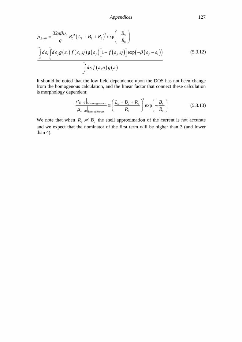
Appendices 127
( )
( ) ( ) ( ) ( ) ( )(
( ) ( )
)
3200 0 0
0
32exp
, 1 , exp
,
i
SE S S
i j i i j j j i
BR L B R
q R
d d g f g f
d f g
ε
πβυµ
ε ε ε ε η ε ε η β ε ε
ε ε η ε
→
∞ ∞
−∞
∞
−∞
⎛ ⎞= + + −⎜ ⎟
⎝ ⎠
⎡ ⎤− −⎣ ⎦∫ ∫
∫
− (5.3.12)
It should be noted that the low field dependence upon the DOS has not been change from the homogenous calculation, and the linear factor that connect these calculation is morphology dependent:
3
0 hom 0
0 0hom
expE in ogenoues S S S
E ogenoues
L B R B
0R R
µ
µ→
→
⎛ ⎞ ⎛+ +≅ ⎜ ⎟ ⎜
⎝ ⎠ ⎝
⎞− ⎟
⎠ (5.3.13)
We note that when 0 SR B the shell approximation of the current is not accurate and we expect that the nominator of the first term will be higher than 3 (and lower than 4).

128 Appendices

Appendices 129
Appendix D: Matlab code for Mobility and Einstein relation MMA calculation
Below given the Matlab function code that calculate mobility, GER, charge carrier concentration and current for hopping (by Miller Abrahams mechanism), a general shape DOS, and homogenous and inhomogeneous materials (for homogenous material the factors Bs and Ls should be inserted as 0). The function should be saved under the name of "polymer_MA3d.m". An example operating m file for a gaussian DOS is given after the function. function [J,Mu,p,ER]=polymer_MA3d(ef,Ro,E,e,de,ge,z,dz,T,NIo,Ls,Bs) %function [J,Mu,p,ER]=polymer_MA(ef,Ro,E,e,de,ge,z,dz,T,NIo,Ls,Bs) % % Transport and occupation factors for Miller Abrahams (MA) model) % % Output: % ER - Einstein relation [kT/q] % p - charge concentration [cm^-3] % J - current density [A/cm^2] % Mu - mobility [cm^2/Vsec] % % Input: % ef - fermi level compare to energy e=0 % Ro - Localization Radii (cm) % E - electrical field Row vector (V/cm). % e - energy vector (eV) % ge - DOS vector (cm^-3eV^-1), ge=G(e) where G(e) is in (cm^-3eV^-1) % ge IS THE SAME LENGTH AS e. % z - Radial Distance vector (cm), min(z)>0 (positive, bigger than 0) % T - Temperature (K), % NIo - Attempt rate (sec^-1), % Ls - site size (advance between jumps) (cm) % Bs - insulator width % % e,ge,z,Rho has to be row vectors, not coloumns. % ef,Ro,E,T,Ls can be row vectors, but not coloumns. % NIo has to be a scalar. % % Yohai Roichman 2003 (c) %
%ef,Ro,E,e,ge,z,Rho,T,NIo,Ls q=1.6e-19; kT=1.38e-23/q.*T; %[eV] % Change ge to units [cm^-3): ge=G(e)*d(e) %%%%%%%%%%%%%%%%%%%%%%%%%%%%%%%%%%%%%%%%% % Charge concentration (p) and Einstein relation (ER) %%%%%%%%%%%%%%%%%%%%%%%%%%%%%%%%%%%%%%%%% for ief=1:size(ef,2) etha=ef(1,ief); fe(ief,:)=1./(1+exp((e-etha)/kT)); % F.D. dist. function pe(ief,1:size(e,2))=ge.*fe(ief,:); % Charge distribution in energy p(ief)=sum(pe(ief,:))*de; % Charge concentration at energy e(ief) ER(ief)=p(ief)./(sum(ge.*exp((e-etha)/kT).*fe(ief,:).^2)*de); % Einstein Relation %--------------------------- % p(e) vs e for different ef %--------------------------- % [pmax,iimax(i)]=max(pe); % figure(1),hold on % plot(pe/pmax,e) end

130 Appendices
% Graphs: p(Ef) and ER(Ef) flag=1; if flag==1 figure(1),subplot(1,2,1),semilogy(ef,p) xlabel('E_F [eV]'),ylabel('p [cm^-^2]') figure(2),subplot(1,2,2),plot(ef,ER) xlabel('E_F [eV]'),ylabel('ER [kT/q]') end
%%%%%%%%%%%%%%%%%%%%%%%%%%%%%%%%%%%%%%%% % Current and Mobilty calculation %%%%%%%%%%%%%%%%%%%%%%%%%%%%%%%%%%%%%%%%
% Create the matrices of zz=z, ee=e, RhoR=Rho, Gee=ge zz=(z'*ones(1,size(e,2)))'; ee=(e'*ones(1,size(z,2))); % Create the matrix Gee=G(e+Ez) Gee=(ge'*ones(1,size(z,2)))*de; %G(E) the DOS - density of states distribution function
% Calculation of the Rhoz(z) dependence for Bs=insulator width, Rho(R)=theta(R-Ls-Bs), % dz=z(2)-z(1); Rz=Ro*(max(zz,Ls+Bs)+Ro).*exp(-(max(zz,Ls+Bs)-Ls)/Ro); %Z*R(z) zRz=dz*zz.*Rz; %Primary loops: for field (E) and ef AND initial energy ei for ief=1:size(ef,2); % ef loop GeFj=(1-1./(1+exp((ee-ef(ief))/kT))).*Gee; % the concentration of unoccupied sites % figure(9),hold off,imagesc(GeFj) ; title('F(fermi dirac) vs e'),pause(5)
for iE=1:size(E,2); % E loop for ie=1:size(e,2) % loop on initial energies ei=e(ie); % GeFjRWij=GeFj*R*Wij for all energies forward + backward jumps GeFjRWij=zRz.*(exp(-(abs(ee-E(iE)*zz-ei)+ee-E(iE)*zz-ei)/2/kT)-… …exp(-(abs(ee+E(iE)*zz-ei)+ee+E(iE)*zz-ei)/2/kT)).*GeFj; jj(ie)=pe(ief,ie)*de*sum(sum(GeFjRWij)); %the total contribution of the jumps from energy end J(ief,iE)=q*2*pi*NIo*sum(jj); % A/cm^2 Mu(ief,iE)=J(ief,iE)/E(iE)/p(ief)/q; % cm^2/Vsec end end
% Graphs: Mu(E) and Mu(Ef) flag=1; if flag==1 figure(3),subplot(1,2,1),loglog(E,Mu) xlabel('E [V/cm]'),ylabel('\mu [cm^-^2eV^-^1]') figure(3),subplot(1,2,2),semilogy(ef,Mu) xlabel('E_F [eV]'),ylabel('\mu [cm^-^2eV^-^1]') end

Appendices 131
The operating m file for a gaussian DOS is given below:
% Transport and occupation factors for Miller Abrahams (MA) model) % by the function % [J,Mu,p,ER]=polymer_MA(ef,Ro,E,e,ge,x,Rho,T,NIo,Ls,dimension) % % Output: % ER - Einstein relation, p - concentration, J - current density, Mu % - mobility % % Input: % ef - fermi level compare to energy e=0 % Ro - Localization Radii (cm) % E - electrical field Row vector (V/cm). % e - energy vector (eV) % ge - DOS vector (cm^-3), ge=G(e)*d(e) where G(e) is in (cm^-3eV^-1) % and d(e) is the increment of vector e (in eV). % ge IS THE SAME LENGTH AS e. % x - Radial Distance vector (cm), min(x)>0 (positive, bigger than 0) % Optional inputs: % Rho - Radial distribution function (Unitless). for the long distances ->1. % IF NOT GIVEN - Rho ASSUMED TO BE UNITY % T - Temperature (K), IF NOT GIVEN - T=300 % NIo - Attempt rate (sec^-1), IF NOT GIVEN - NIo=1 % Ls - site size (advance between jumps) (cm) IF NOT GIVEN - Ls=0 % dimension - 1 for 1D, 3 for 3D. IF NOT GIVEN - dimension=1 % % e,ge,x,Rho has to be row vectors, not coloumns. % ef,Ro,E,T,Ls can be row vectors, but not coloumns. % NIo has to be a scalar. % % Yohai Roichman 2003 (c)
clear
% Constants for convenience q=1.6e-19; RT=300; %Room Temperature kT=1.38e-23/q*RT;
% the function polymer_MA "Must" parameters (inputs): % ef, Ro, E, e, ge, x, Rho, T, NIo, Ls, dimension ef=[-50:5:-10 -8:2:0]*kT; % Ef vector Ro=1e-9; % Localization radii E=10.^[2:0.1:9]; % Electrical field vector (row) e=[-50:0.25:50]*kT; % energy vector (initial and final) (row) ge=normpdf(e,0,5*kT)*1e20*0.25*kT; %g(E)=normalized g(E)* Nv*dE. % THE UNITS are [cm^-3] because ge=Ge[cm^-3eV^-1]*de[eV] x=[1e-10:1e-10:10e-9]; % x=length vector[cm] % Optional parameters (inputs) Rho = ones(size(x)); % Rho - Radial distribution function (Unitless). T=300; % T - Temperature (K) NIo = 1e12; % NIo - Attempt rate (sec^-1) Ls = 0; % Ls - site size (advance between jumps) (cm) dimension=3; % dimension - 1 for 1D, 3 for 3D.
[J,Mu,p,ER]=polymer_MA(ef,Ro,E,e,ge,x,Rho,T,NIo,Ls,dimension);
save 'data.mat'
% Graphs: p(Ef) and ER(Ef) figure(1),subplot(1,2,1),semilogy(ef,p) xlabel('E_F [eV]'),ylabel('p [cm^-^2]') grid on, hold on, figure(1),subplot(1,2,2),plot(ef,ER) xlabel('E_F [eV]'),ylabel('ER [kT/q]') grid on, hold on, % Graphs: Mu(E) and Mu(Ef) figure(2),subplot(1,2,1) loglog(E,Mu) xlabel('E [V/cm]'),ylabel('\mu [cm^-^2eV^-^1]') grid on figure(2),subplot(1,2,2) semilogy(ef,Mu) xlabel('E_F [eV]'),ylabel('\mu [cm^-^2eV^-^1]') grid on

132 Appendices

Appendices 133
Appendix E: Process procedure for bottom contact PFET substrates
In this appendix a detailed procedure to produce low leakage, low threshold shift substrate for organic field effect transistors is described, as a process sheet.
Date:___________ Run (oxidation):__________
Wafers: Si (100) p-type (B doped) ρ≤0.003 Ωcm No. Name Process Measurements
1 Pre oxidation cleaning (RCA):
1) H2SO4:H2O2 (3:1) @ 100°C, 10 min. DI water 14 MΩ. 2) HF:H2O (1:50) @ RT 15 sec. DI water 14 MΩ. 3) NH4OH:H2O2:H2O (1:1:4) @ 80°C, 10 min. DI water 14 MΩ.
2 Dry oxidation: 1000°C, 30 min. (~25nm). Oxide strip: Buffer oxide etch @ RT, 90 sec. 950°C, 250 min. (~80nm).
Oxide thickness. C-V.
3 Evaporation Ti:Au Evaporation Ti: 5nm, Au: 50nm. 4 Level 0:
Back contact photolithography
(Au:Ti:SiO2)
1) P.R. AZ2020: 4000 rpm, 60 sec. 2) Prebake: 110°C, 1 min., hot plate. 3) Exposure: 2 sec. 4) PEB: 110°C, 1 min., hot plate. 5) Developer: 25 sec.
Visual. α-step (optional) after developer.
Redevelop if necessary.
5 Etching Au:Ti:Oxide
1) Au etch: KI:I2:H2O (50gr:200gr:200ml) RT, ~3 sec. DI water rinse: 2 min. 2) Ti etch: HF:H2O 1:50, 30 sec., RT.
DI water rinse: 14 MΩ. 3) SiO2 etch: BHF, 100 sec., RT.
DI water rinse: 2 min. 4) Hardbake: 90°C, 10 min. 5) Plasma descum: 200mTorr O2, 100W, 2 min.
Visual inspection after every step. α-step (optional)
6 Evaporation: Al Evaporation Al/Cr/Si 100nm. instead of silver paint-optional
7 Lift-off for Al 1) NMP, 50-60°C, 2min. 2) Ultrasonic bath, Aceton, 5 min. 3) Plasma descum: 200mTorr O2, 100W, 2 min.
instead of silver paint-optional
8 Level 1: FETs
photolithography (Au:Ti)
1) Priming 120°C, 10 min., hot plate. 2) P.R. 5214E: 5000 rpm, 60 sec. 3) Prebake: 90°C, 15 min., Oven. 4) Exposure: 4.7 sec. 5) Developing: 60 sec. 6) Plasma descum: 200mTorr O2, 100W, 2 min. 7) Postbake: 90°C, 20 min., Oven.

134 Appendices
9 Etching Au:Ti 1) Au etch: I2:NH4I:H2O:C2H5OH (0.5gr:2gr:10ml:15ml) @ RT, 45 sec. DI water rinse: 2 min. 2) P.R. strip: DMF, 5 min. @ 140°C, hot plate. DI water rinse: 2 min. 3) Ti etch: NH4OH:H2O2:H2O (1:1:4), 60 sec. @ RT.
DI water rinse: 15 MΩ.
10 Final tests Visual inspection: AFM: Dimensions: L: Lmeasured: . (Vickers-optional) L: Lmeasured: . L: Lmeasured: . Ti-Au thickness: . Au underetch . Nanospec: final oxide thickness: . Break down voltage of oxide: .
C-V (optional): VT shift of SiO2 layer on lightly
diluted Si:
In glove-box
11 Polymer solution MEHPPV solution preparation, Standard dehydrated Toluene + MEHPPV 85oC ~ 60 min – till fully dissolved.
12 Transistor process Back contact (for no Al chips): Scratch + silver paint brush. Spin coat MEH: 1400 rpm, 80 sec Thermal treatment: 120 min 90oC (ramp up 60 min, ramp down 60 min)

Appendices 135
Appendix F: Accumulation layer width The PFET characteristics analysis provides the mobility dependence on
surface charge concentration. Moreover the analysis methods introduced in the former section relies on a linear relation between the local surface potential and the surface charge concentration (Eq. (3.5.4)). These relations relies on the assumption that the charge distribution on the perpendicular direction to the insulator layer ( ) can be approximated to a delta function of charges at the polymer semiconductor-insulator interface. However the charge is spread on this direction to a layer that is the order of magnitude of the Debye electrostatic screening length, which depends on
y
D µ ratio, namely, on the generalized Einstein relation (GER). This stems from the equality between the drift current toward the gate electrode and the diffusion current that is on the other direction. In section 2.3.3 we demonstrated that the GER is strongly depend on the charge concentration. In this section we demonstrate how this effect the effective charge concentration in the PFET channel. Below is given the accumulation layer width calculation as obtained by N. Tessler140.
In the development of the I-V characteristics we did not consider the charge
density profile along the x-axis, figure 77. This was justified by the assumption that ϕs (the interface potential) is constant once the transistor is above threshold. In other words, we neglected any changes in the charge profile and the associated change in the voltage drop across it. Adding this effect rigorously will significantly complicate the expressions as for each point along the y axis there exist a different effective capacitance and . _ _ ( ,Ins Ins EFF Ins EFF GSC C C V⇒ = )y
-1
-0.8
-0.6
-0.4
-0.2
0
5 1016
1 1017
-100 -50 0 50Distance from Insulator (nm)
Cha
rge
Den
sity
(cm
-3)
Pote
ntia
l (V
)
Gate πInsulator
XChannel
Figure 77. Simulated charge density (2D simulation) and potential at the middle of the channel for p-channel transistor and a bias of VDS=(VGS-VT)=-1. XChannel denotes the effective channel depth (~7nm here).

136 Appendices
In the present text we try instead to examine the validity of our assumption
and give the reader a feeling for the associated effect on the device performance. To derive and expression for the charge profile perpendicular to the insulator we start with the basic current continuity and Poisson equations:
( )
0
h h h h hJ qp E q D p qp E qD p qp Dhx x xE p qxπ
µ µ
ε ε
∂ ∂= ⋅ − = ⋅ − −
∂ ∂∂
= ⋅∂
∂∂ (5.6.1)
At steady-state there is no current flow in the x direction and if we assume*
h hD p p Dx x
∂ ∂>>
∂ ∂ we arrive at:
0h h hpJ qp E qDx
µ ∂= ⋅ − =
∂ (5.6.2)
and the boundary conditions for the electric field are:
0
( );G
insxins
V V yE E E
d π=0
x d=
−= ≈ = (5.6.3)
using Eq. (5.6.2) and the Poisson equation we can derive:
2
2
h
h
DEEx
Exµ
∂ ∂=
∂ ∂ (5.6.4)
or
2
12
h
h
D EEx x xµ
∂ ∂ ∂=
∂ ∂ ∂ (5.6.5)
Integrating over x once (assuming D/µ to be a slowly varying function of x)*:
2
2h
h
EE CD x
µ ∂+ =
∂ (5.6.6)
where C is a constant to be determined by the boundary conditions. Integrating between point x to the air interface (dπ) we arrive at:
0
2
'''
2
d
hx E
h
ExE C
D
π
µ∂
∂ =+
∫ ∫ (5.6.7)
and finally:
(
2tan
2h h
h h
CD CE
Dµ
µ)x L
⎡ ⎤= −⎢ ⎥
⎢ ⎥⎣ ⎦ (5.6.8)
* see section 2.3.3 regarding the charge-density dependence of Dh or of D/µ.

Appendices 137
( )2
0 0 tan 12
h
h
C CEpq x q D
π πε ε ε ε µ⎛ ⎞⎡ ⎤∂ ⎜= = −⎢⎜ ⎟∂ ⎢ ⎥⎣ ⎦⎝ ⎠
x L ⎟+⎥ (5.6.9)
and C is to be determined by:
(
2tan 0
2h h
insh h
CD CE
Dµ
µ)L
⎡ ⎤= −⎢ ⎥
⎢ ⎥⎣ ⎦ (5.6.10)
To illustrate the use of Eqs. (5.6.8) to (5.6.10) we calculated the charge density profile for two different electric fields at the insulator (E0). The first one was chosen to be close to the conditions used for figure 77 and the second for a higher applied voltage. We first use Eq. (5.6.10) to find the integration constant C (Table 4) and then use Eq. (5.6.9) to calculate the charge density profile.
Eins [v/cm] dπ [cm] C
5⋅104 50⋅10-7 3.5457e+009 3⋅105 50⋅10-7 4.7943e+009
Table 4. The parameters used for Fig. 78.
0
1 1018
2 1018
3 1018
0
5 1016
1 1017
0 10 20 30 40 50
Cha
rge
Den
sity
(cm
-3) Charge D
ensity (cm-3)
Distance From Insulator (nm)
0
1 1018
2 1018
3 1018
0 2 4 6 8 10
D kTqµ
=
2D kTqµ
= ⋅
Figure 78. Calculated charge density profile for two electric fields near the insulator (different VGS). The right axis is for and the left axis for ( 3
40 5 10 [V/cm]ε = ⋅
50 3 10 [V/cm]ε = ⋅ πε = ). The inset shows the effect of D µ being
a (slowly-varying) function of the charge density ( ). The full line in the inset was calculated using
40 5 10 [V/cm]ε = ⋅
2D kT qµ = (see Fig. 24 in 140) and only the first 10nm are shown.
Examining figure 78 we note that at low voltage drop across the insulator the
channel is rather extended and a significant charge density exists all across the

138 Appendices
π-conjugated layer. The functional form of the density distribution tells us that for a thinner π-conjugated layer the effect will be more pronounced. We also note that at higher applied bias the channel becomes more confined as most of the added charge accumulates near the insulator interface. Finally, the inset shows the effect of the enhanced Einstein-relation as discussed in section 2.3.3.
To extract a simple expression for the voltage drop across the channel we rely again on the fact that at steady-state no current flows in the x direction and use the following expression (see 149):
12 1 2 1
1
exp( [ ])XX X X X
X
n nDµ
φ φ= − − (5.6.11)
If we let X1 be at the channel and X2 at the bulk then the voltage drop due to charge accumulation at the channel (that we have neglected in section 3.5) is 2 1( )X Xφ φ φ∆ = − .
0ln x
x d
nDn
π
πφµ
=
=
⎛ ⎞⎜∆ = −⎜⎝ ⎠
⎟⎟
(5.6.12)
Using the results for the charge density shown in figure 78 we arrive at 2.7 Dπφ
µ∆ = −
and 5.9 Dπφ
µ∆ = − for the low and high fields, respectively. As figure 78 was
calculated for 26 [meV]D kT qµ = = the voltage drops are 70 [meV] and 150 [meV], respectively.
One may argue that the boundary condition (5.6.3) should now be rewritten as:
0
( );G
insxins
V V yE E E
d π
π 0x d
φ= =
− − ∆= ≈ = (5.6.13)
and equations (5.6.8) to (5.6.13) should be solved iteratively. Using the iterative approach one finds that the voltage drops are 64meV and 151meV suggesting that a single iteration is typically sufficient. To make the picture complete we mention that it has been shown that organic amorphous (disordered) semiconductors are degenerate at all practical densities115 and hence D kT qµ η= with η being a function of the charge density (see also section 2.3.3). For example, using the calculation shown in the inset to figure 78 ( 2η = ) 0.25Max eVφ∆ ≅ .
Next we move to evaluate a simple expression also for the effective channel depth. If we define XChannel as the point where p drop to 1/e of its value then
1 1 1
2 1 1
112 12exp( )x x x
ins Channelx x x
p D De Ep D
Xµ
φ φµ µ
= = − ∆ → ∆ = − = (5.6.14)
If we assume that within the channel depth the electric field has not decayed significantly from its value at the insulator:
ins ChannelE X D µ= (5.6.15)
and

Appendices 139
( )
insChannel
G
d kTXV V y q
η≈−
(5.6.16)
Using common parameters as 100 7 ; 1 ; 1ins GS T DSd e cm V V V V V= − − = = we find that near the source ( ) ( )G GSV V y V− = 2.6 nmchannelX η= × and at the centre of the
channel ( )( ) 0.5G TV V y V V− − ≅ 5.2 nmchannelX η= × . Note that the approximate expression of Eq. (5.6.15) is in good agreement with the numerical simulation results shown in figure 77. Namely, in organic transistor where the molecular distance is about 0.5 [nm] the channel will extend over several monolayers, especially at low gate bias.

140 Appendices

Appendices 141
Appendix G: The measured polymer field effect transistors properties
In the next table we summarized the technical data of the measured polymer field effect transistors that were presented in the thesis. All of the transistor were made of MEH-PPV ADS-100RE from 4 different batches (two with MW 100k, MW 1M and MW 2.8 M), that were dissolved in Toluene. The transistor were fabricated in process that is presented in appendix E or similar to it. We found variations between the measured high concentration mobility between transistors made of the same material.
Num. Figures MW
[gr/mole] Design W
[ ]mµ L
[ m]µtox
[nm] VT [V]
high biasµ − 2 [cm / sec]V
A 52.a
53 100k BOC
+Polyimide6000 20 80 ~-1 58 10−⋅
B 52.b 53
100k TOC 6000 40 80 ~-1.5 55 10−⋅
C 58 100k BOC+ Close
topology
11,000 10 80 ~-2 52 10−⋅
D 59,60,62 1M BOC +Polyimide
6000 17.5 67 ~-1.8 42 10−⋅
E 65,68 100k BOC+ Close
topology
11,000 9.5 25 ~-1.8 51.5 10−⋅
F 66 100k BOC+ Close
topology
11,000 9.5 25 ~-1.8 51.7 10−⋅
G 67 100k BOC +Polyimide
6000 9.5 80 ~-2.5 57 10−⋅
H1 70 100k BOC +Polyimide
6000 9.5 80 ~-2.5 51.2 10−⋅
H2 70 1M BOC +Polyimide
6000 9.5 80 ~-2.5 52 10−⋅
H3 69,70 2.8M BOC +Polyimide
6000 9.5 80 ~-2.5 57 10−⋅
I 71 2.8M BOC+ Close
topology
11,000 11.5 75
J 71 100k BOC +Polyimide
6000 11 80
Table 5: Technical data of the measured PFETs.

142
Bibliography

Bibliography 143
Bibliography
1 C. K. Chiang, C. R. Fincher, Y. W. Park, A. J. Heeger, H. Shirakawa, E. J. Louis, S. C. Gau, and A. G. MacDiarmid, Phys. Rev. Lett. 39, 1098-1101 (1977).
2 J. H. Burroughes, C. A. Jones, and R. H. Friend, Nature 335, 137-141 (1988). 3 H. Scher and E. W. Montroll, Physical Review B (Solid State) 12, 2455-77
(1975). 4 H. Scher, M. F. Shlesinger, and J. T. Bendler, Physics Today 44, 26-34
(1991). 5 G. Horowitz and P. Delannoy, Journal of Applied Physics 70, 469-475 (1991). 6 C. P. Jarrett, R. H. Friend, A. R. Brown, and D. M. Deleeuw, Journal of
Applied Physics 77, 6289-6294 (1995). 7 M. Vissenberg and M. Matters, Physical Review B 57, 12964-12967 (1998). 8 H. Bassler, Physica Status Solidi B - Basic Research 175, 15-56 (1993). 9 P. M. Chaikin and T. C. Lubensky, Principle of condensed matter physics
(Cambridge University Press, Cambridge, 1997). 10 A. Einstein, Annalen der Physik 17, 549-560 (1905). 11 N. W. Ashcroft and N. D. Mermin, Solid State Physics (Harcourt College
Publishers, 1976). 12 E. W. Montroll and G. H. Weiss, Journal of Mathematical Physics 6, 167-&
(1965). 13 H. Scher and M. Lax, Physical Review B 7, 4491-502 (1973). 14 R. Metzler and J. Klafter, Physics Reports 339, 1-77 (2000). 15 J. Klafter and R. Silbey, Physical Review Letters 44, 55-58 (1980). 16 P. W. Anderson, Phys. Rev. 109, 1492-1505 (1958). 17 N. F. Mott and E. A. Davis, Electronic processes in non-crystalline materials,
Second ed. (Calderon Press, Oxford, 1979). 18 N. Tessler, in Lectures on organic semiconductors devices (Nir Tessler's Web-
site, http://www.ee.technion.ac.il/people/nir/Lectures.html, 2001). 19 D. Moses, J. Wang, A. J. Heeger, N. Kirova, and S. Brazovski, Proceedings of
the National Academy of Sciences of the United States of America 98, 13496-13500 (2001).
20 D. Moses, R. Schmechel, and A. J. Heeger, Synthetic Metals 139, 807-810 (2003).
21 M. Chandross, S. Mazumdar, M. Liess, P. A. Lane, Z. V. Vardeny, M. Hamaguchi, and K. Yoshino, Physical Review B 55, 1486-1496 (1997).
22 C. Im, W. Tian, H. Bassler, A. Fechtenkotter, M. D. Watson, and K. Mullen, Journal of Chemical Physics 119, 3952-3957 (2003).
23 J. L. Bredas, J. Cornil, D. Beljonne, D. dos Santos, and Z. G. Shuai, Accounts of Chemical Research 32, 267-276 (1999).
24 M. A. Pasquinelli, Ph.D. Thesis, Carnegie Mellon University, 2002. 25 P. G. Dacosta and E. M. Conwell, Physical Review B 48, 1993-1996 (1993). 26 S. C. Graham, D. D. C. Bradley, R. H. Friend, and C. Spangler, Synthetic
Metals 41, 1277-1280 (1991). 27 D. D. C. Bradley, J. PHYS. D-APPL PHYS. 20, 1389-1410 (1987). 28 G. H. Gelinck, J. J. Piet, B. R. Wegewijs, K. Mullen, J. Wildeman, G.
Hadziioannou, and J. M. Warman, Physical Review B 62, 1489-1491 (2000).

144 Bibliography
29 J. Rissler, H. Bassler, F. Gebhard, and P. Schwerdtfeger, Physical Review B 6404 (2001).
30 A. Kohler, D. A. dos Santos, D. Beljonne, Z. Shuai, J. L. Bredas, A. B. Holmes, A. Kraus, K. Mullen, and R. H. Friend, Nature 392, 903-906 (1998).
31 K. F. Voss, C. M. Foster, L. Smilowitz, D. Mihailovic, S. Askari, G. Srdanov, Z. Ni, S. Shi, A. J. Heeger, and F. Wudl, Physical Review B 43, 5109-5118 (1991).
32 I. D. Parker, Journal of Applied Physics 75, 1656-1666 (1994). 33 E. M. Conwell and H. A. Mizes, Physical Review B 51, 6953-6958 (1995). 34 H. A. Mizes and E. M. Conwell, Physical Review Letters 70, 1505-1508
(1993). 35 Z. Shuai, D. Beljonne, and J. L. Bredas, Solid State Communications 78, 477-
480 (1991). 36 H. A. Mizes and E. M. Conwell, Synthetic Metals 68, 145-151 (1995). 37 H. Y. Choi and M. J. Rice, Physical Review B 44, 10521-10524 (1991). 38 E. M. Conwell, Physical Review B 57, R12670-R12672 (1998). 39 S. V. Rakhmanova and E. M. Conwell, Applied Physics Letters 75, 1518-1520
(1999). 40 D. M. Basko and E. M. Conwell, Physical Review Letters 88, 056401-056404
(2002). 41 A. Schenning, A. C. Tsipis, S. C. J. Meskers, D. Beljonne, E. W. Meijer, and
J. L. Bredas, Chemistry of Materials 14, 1362-1368 (2002). 42 M. Malagoli, M. Manoharan, B. Kippelen, and J. L. Bredas, Chemical Physics
Letters 354, 283-290 (2002). 43 H. Bassler, Phys. stat. sol. (b) 107, 9-56 (1982). 44 P. W. M. Blom and M. Vissenberg, Physical Review Letters 80, 3819-3822
(1998). 45 D. Monroe, Physical Review Letters 54, 146-149 (1985). 46 D. Monroe and M. A. Kastner, Physical Review B 33, 8881-8884 (1986). 47 E. A. Schiff, Physical Review B 24, 6189-6192 (1981). 48 T. Tiedje, J. M. Cebulka, D. L. Morel, and B. Abeles, Physical Review Letters
46, 1425-1428 (1981). 49 M. Grunewald, P. Thomas, and D. Wurtz, Physica Status Solidi B-Basic
Research 94, K1-K4 (1979). 50 K. P. Ghatak, A. K. Chowdhury, S. Ghosh, and A. N. Chakravarti, Acta
Physica Polonica A 58, 389-395 (1980). 51 K. P. Ghatak, A. K. Chowdhury, S. Ghosh, and A. N. Chakravarti, Physica
Status Solidi B-Basic Research 99, K55-K60 (1980). 52 H. Scher and M. Lax, Physical Review B 7, 4502-19 (1973). 53 M. Silver, G. Schonherr, and H. Bassler, Philosophical Magazine B-Physics of
Condensed Matter Statistical Mechanics Electronic Optical and Magnetic Properties 43, 943-947 (1981).
54 G. Schonherr, H. Bassler, and M. Silver, Philosophical Magazine B-Physics of Condensed Matter Statistical Mechanics Electronic Optical and Magnetic Properties 44, 47-61 (1981).
55 H. Bassler, Physica Status Solidi B-Basic Research 107, 9-54 (1981). 56 H. Bassler, G. Schonherr, M. Abkowitz, and D. M. Pai, Physical Review B 26,
3105-3113 (1982).

Bibliography 145 57 S. F. Alvarado, S. Barth, H. Bassler, U. Scherf, J. W. van der Horst, P. A.
Bobbert, and M. A. J. Michels, Advanced Functional Materials 12, 117-122 (2002).
58 S. F. Alvarado, L. Rossi, P. Muller, P. F. Seidler, and W. Riess, Ibm Journal of Research and Development 45, 89-100 (2001).
59 N. F. Mott and W. D. Twose, Advances in Physics 10, 107 (1961). 60 A. Miller and E. Abrahams, Phys. Rev. 120, 745-755 (1960). 61 R. A. Marcus, Journal of Chemical Physics 24, 966-978 (1956). 62 R. A. Marcus and N. Sutin, Biochimica Et Biophysica Acta 811, 265-322
(1985). 63 R. A. Marcus, Reviews of Modern Physics 65, 599-610 (1993). 64 T. Holstein, Annals of physics 8, 325 (1959). 65 T. Holstein, Annals of physics 8, 343 (1959). 66 D. Emin and T. Holstein, Physical Review Letters 36, 323-326 (1976). 67 H. Scher and T. Holstein, Bulletin of the American Physical Society 22, 458-
459 (1977). 68 H. Scher and T. Holstein, Philosophical Magazine B - Physics of Condensed
Matter Statistical Mechanics Electronic Optical and Magnetic Properties 44, 343-56 (1981).
69 D. Emin, Physical Review B 61, 14543-14553 (2000). 70 M. Pope and C. E. Swenberg, Electronic processes in organic crystals and
polymers, 2nd ed. (Oxford University Press, New York, 1999). 71 D. Emin, Physical Review Letters 25, 1751-& (1970). 72 D. Emin, Advances in Physics 24, 305-348 (1975). 73 D. H. Dunlap, P. E. Parris, and V. M. Kenkre, Physical Review Letters 77,
542-545 (1996). 74 Z. G. Yu, D. L. Smith, A. Saxena, R. L. Martin, and A. R. Bishop, Physical
Review B 6308 (2001). 75 D. J. Pinner, R. H. Friend, and N. Tessler, J. Appl. Phys. 86, 5116-5130
(1999). 76 H. Kageyama, K. Ohnishi, S. Nomura, and Y. Shirota, Chemical Physics
Letters 277, 137-141 (1997). 77 A. Peled, L. B. Schein, and D. Glatz, Physical Review B 41, 10835-10844
(1990). 78 G. Pfister and H. Scher, Physical Review B (Solid State) 15, 2062-83 (1977). 79 A. B. Walker, A. Kambili, and S. J. Martin, Journal of Physics-Condensed
Matter 14, 9825-9876 (2002). 80 S. V. Novikov, D. H. Dunlap, V. M. Kenkre, P. E. Parris, and A. V. Vannikov,
Physical Review Letters 81, 4472-4475 (1998). 81 Y. N. Gartstein and E. M. Conwell, Physical Review B 51, 6947-6952 (1995). 82 H. Cordes, S. D. Baranovskii, K. Kohary, P. Thomas, S. Yamasaki, F. Hensel,
and J. H. Wendorff, Physical Review B 6309, 4201-+ (2001). 83 D. H. Dunlap, Physical Review B 52, 939-954 (1995). 84 Fishchuk, II, A. Kadashchuk, H. Bassler, and S. Nespurek, Physical Review B
67 (2003). 85 V. I. Arkhipov, P. Heremans, E. V. Emelianova, G. J. Adriaenssens, and H.
Bassler, Chemical Physics 288, 51-55 (2003). 86 S. Rackovsky and H. Scher, Journal of Chemical Physics 111, 3668-74 (1999). 87 Y. N. Gartstein and E. M. Conwell, Chemical Physics Letters 245, 351-358
(1995).

146 Bibliography
88 S. Marianer and B. I. Shklovskii, Physical Review B 46, 13100-13103 (1992). 89 M. Abkowitz and H. Scher, Philosophical Magazine 35, 1585-608 (1977). 90 E. Muller-Horsche, D. Haarer, and H. Scher, Physical Review B-Condensed
Matter 35, 1273-80 (1987). 91 F. C. Bos, T. Guion, and D. M. Burland, Physical Review B 39, 12633-12641
(1989). 92 R. Richert, L. Pautmeier, and H. Bassler, Phys. Rev. Lett. 63, 547-550 (1989). 93 X. Jiang, Y. Harima, K. Yamashita, Y. Tada, J. Ohshita, and A. Kunai,
Chemical Physics Letters 364, 616-620 (2002). 94 V. I. Arkhipov, P. Heremans, E. V. Emelianova, G. J. Adriaenssens, and H.
Bassler, Applied Physics Letters 82, 3245-3247 (2003). 95 V. I. Arkhipov, E. V. Emelianova, and G. J. Adriaenssens, Physical Review B
6412 (2001). 96 G. Juska, K. Genevicius, R. Osterbacka, K. Arlauskas, T. Kreouzis, D. D. C.
Bradley, and H. Stubb, Physical Review B 67 (2003). 97 R. Osterbacka, Personal Communication. 98 F. C. Bos and D. M. Burland, Physical Review Letters 58, 152-155 (1987). 99 P. K. Weimer, 1962, p. 1462. 100 S. M. Sze, Physics of Semiconductor Devices (Wiley, New York, 1981). 101 T. Ando, A. B. Fowler, and F. Stern, Reviews of Modern Physics 54, 437-672
(1982). 102 O. Katz, A. Horn, G. Bahir, and J. Salzman, Ieee Transactions on Electron
Devices 50, 2002-2008 (2003). 103 A. R. Brown, C. P. Jarrett, D. M. deLeeuw, and M. Matters, Synthetic Metals
88, 37-55 (1997). 104 G. Horowitz, R. Hajlaoui, and P. Delannoy, Journal De Physique Iii 5, 355-
371 (1995). 105 E. J. Meijer, C. Tanase, P. W. M. Blom, E. van Veenendaal, B. H. Huisman,
D. M. de Leeuw, and T. M. Klapwijk, Applied Physics Letters 80, 3838-3840 (2002).
106 C. Tanase, E. J. Meijer, P. W. M. Blom, and D. M. de Leeuw, Physical Review Letters 91, 216601-216604 (2003).
107 A. Aleshin, R. Kiebooms, R. Menon, and A. J. Heeger, Synthetic Metals 90, 61-68 (1997).
108 G. Horowitz, R. Hajlaoui, H. Bouchriha, R. Bourguiga, and M. Hajlaoui, Advanced Materials 10, 923-+ (1998).
109 L. M. Cameron and C. A. Sholl, Journal of Physics-Condensed Matter 11, 4491-4497 (1999).
110 L. Burgi, H. Sirringhaus, and R. H. Friend, Applied Physics Letters 80, 2913-2915 (2002).
111 Y. Preezant, M.Sc. Thesis, Technion - IIT, 2004. 112 D. Ritter, E. Zeldov, and K. Weiser, Physical Review B 38, 8296-8304 (1988). 113 Y. F. Chyan, S. M. Sze, C. Y. Chang, K. Liao, and R. Reif, Japanese Journal
of Applied Physics Part 1-Regular Papers Short Notes & Review Papers 33, 2619-2625 (1994).
114 M. I. Kaganov and V. B. Fiks, Journal of Statistical Physics 38, 329-345 (1985).
115 Y. Roichman and N. Tessler, Applied Physics Letters 80, 1948-1950 (2002). 116 V. Savvateev, A. Yakimov, and D. Davidov, Advanced Materials 11, 519-+
(1999).

Bibliography 147 117 Y. Roichman, Y. Preezant, and N. Tessler, Physica Status Solidi A-Applied
Research 201, 1246-1262 (2004). 118 P. J. McKelvey, Solid state physics for engineering and material science
(Krieger pbulishing company, Malabar, Florida, 1993). 119 R. A. Smith, Semiconductors, 2nd ed. (Cambridge university press, London,
New York, Melbourne, 1978). 120 Fishchuk, II, D. Hertel, H. Bassler, and A. K. Kadashchuk, Physical Review B
65 (2002). 121 D. H. Dunlap, Journal of Imaging Science and Technology 40, 291-298
(1996). 122 A. J. Mozer and N. S. Sariciftci, Chemical Physics Letters 389, 438-442
(2004). 123 Y. Preezant and N. Tessler, (To be published). 124 S. Shaked, S. Tal, Y. Roichman, A. Razin, S. Xiao, Y. Eichen, and N. Tessler,
Advanced Materials 15, 913-+ (2003). 125 Y. Roichman and N. Tessler, Kerkrede, 2001. 126 H. C. F. Martens, P. W. M. Blom, and H. F. M. Schoo, Phys. Rev. B 61, 7489-
7493 (2000). 127 S. V. Rakhmanova and E. M. Conwell, Applied Physics Letters 76, 3822-3824
(2000). 128 A. Kadashchuk, Y. Skryshevskii, A. Vakhnin, N. Ostapenko, V. I. Arkhipov,
E. V. Emelianova, and H. Bassler, Physical Review B 6311 (2001). 129 M. A. Baldo, Z. G. Soos, and S. R. Forrest, Chemical Physics Letters 347,
297-303 (2001). 130 T. Q. Nguyen, I. B. Martini, J. Liu, and B. J. Schwartz, Journal of Physical
Chemistry B 104, 237-255 (2000). 131 V. I. Arkhipov and H. Bassler, Phil. Mag. Lett. 69, 241-246 (1994). 132 J. M. Ziman, Models of disorder (Cambridge university press, Cambridge,
1979). 133 Y. Roichman and N. Tessler, Applied Physics Letters 80, 151-153 (2002). 134 N. Tessler and Y. Roichman, Applied Physics Letters 79, 2987-2989 (2001). 135 M. Nonnenmacher, M. P. Oboyle, and H. K. Wickramasinghe, Applied
Physics Letters 58, 2921-2923 (1991). 136 R. Shikler, T. Meoded, N. Fried, and Y. Rosenwaks, Applied Physics Letters
74, 2972-2974 (1999). 137 H. Sugimura, Y. Ishida, K. Hayashi, O. Takai, and N. Nakagiri, Applied
Physics Letters 80, 1459-1461 (2002). 138 S. Belaidi, F. Lebon, P. Girard, G. Leveque, and S. Pagano, Applied Physics
a-Materials Science & Processing 66, S239-S243 (1998). 139 L. Burgi, R. H. Friend, and H. Sirringhaus, Applied Physics Letters 82, 1482-
1484 (2003). 140 N. Tessler and Y. Roichman, edited by J. C. deMello and J. J. M. Halls (Wiley
and Son). 141 O. Katz, Y. Roichman, G. Bahir, N. Tessler, and J. Salzman, Journal of
Applied Physics (submitted). 142 G. Horowitz, R. Hajlaoui, D. Fichou, and A. El Kassmi, Journal of Applied
Physics 85, 3202-3206 (1999). 143 G. Horowitz and M. E. Hajlaoui, Synth. Met. 122, 185-189 (2001). 144 G. Horowitz, Polycrystalline Semiconductors IV Mater., Technologies &
Large Area Electronics 80-81, 3-13 (2001).

148 Bibliography
145 R. E. Williams, (Artech House, Dedham MA, 1984), p. 371-381. 146 Y. Roichman and N. Tessler, Synthetic Metals 135, 443-444 (2003). 147 E. W. Meijer, C. Detcheverry, P. J. Baesjou, E. van Veenendaal, D. M. De
leeuw, and T. M. Klapwijk, Journal of Applied Physics 93, 4831-4835 (2003). 148 M. S. Nam, A. Ardavan, R. J. Cava, and P. M. Chaikin, Applied Physics
Letters 83, 4782-4784 (2003). 149 Y. Preezant and N. Tessler, Journal of Applied Physics 93, 2059-2064 (2003).