Embed Size (px)
Citation preview

Characterization of Wavelength Tunable Lasers For Use in Wavelength Packet Switched Networks
By
Antonia D antcha B. Eng., MI KEF,
A TH ESIS SU BM ITTED F O R T H E D E G R E E O F
M aster o f Engineering
In the School o f Electronic Engineering.
D ublin City University
Research Supervisor
Dr. Liam Barry
March 2005
1

Approval
Name: Antonia Dantcha
Degree: Master o f Engineering
Title o f Thesis: Characterization of Wavelength Tunable Lasers
For Use in Wavelength Packet Switched Networks
Examining Committee: 1. Internal Examiner: Dr. Pascal Landais,
Electronic Engineering, Dublin City University
2. External Examiner: Prof. Jcan-Claudc Simon.
Université de Rennes 1, France
2

I hereby certify that this material, which I now submit for assessment on the programme of
study leading to the award of Master in Engineering is entirely my own work and has not
been taken from the work of others save and to the extent that such work has been cited and
acknowledged within the text of my work.
ID No. : 5 Z \ ~ V ^ Q\ C Q
Date: 2 ^ / 0 & j Q Si
3

AbstractThe telecom industry's greatest challenge, and the optical systems and components
vendors' biggest opportunity is enabling providers to expand their data services. The solution
lies in making optical networks more responsive to customer needs, i.e., making them more
rapidly adaptable. One possible technique to achieve this is to employ wavelength tunable
optical transmitters. The importance of tunability grows greater every year, as the average
number of channels deployed on DWDM platforms increases. By deploying tunable lasers it
is much easier to facilitate forecasting, planning and last minute changes in the network. This
technology provides with solution for inventory reduction. It also offers solution for fast
switching at packet level.
The conducted research activities o f the project was divided in two work packages:
1. Full static characterization-the laser used in the experiment was a butterfly-packaged
Sampled Grating DBR laser with four electrically tunable sections. LabView programme was
developed for distant control o f the equipment and the laser itself. The parameters required
for creating a look-up table with the exact currents for the four sections of the laser, namely
wavelength, side mode suppression ratio and output power, were transferred to tables. Based
on those tables the currents were defined for each o f the 96 different accessible channels. The
channel allocation is based on the 50 GHz spacing grid. A detailed analysis of the tuning
mechanisms is provided.
2. Dynamic characterization and BER performance in wavelength packet switched
WDM systems-a commercially available module was used supplied with the software
package for controlling the wavelength channels and setting the laser to switch between any
accessible channel. The laser is DBR laser without SOA integration so the dynamic tunability
can be investigated. As the switching in the nanosecond regime is executed in the electrical
domain, analysis o f the switching parameters concerning the electrical circuit as well as laser
structure is provided. The actual switching time was defined. The degradation in system
performance due to spurious wavelength signals emitted from the tunable module during the
switching event and their interference with other active channels was demonstrated by
examining the presence of an error floor in the BER rate against received power
measurements.
5

Table of contentsA pproval 2
Declaration 3
Acknowledgements 4
1. Optical Com m unication Networks 10
1.1. The basics 10
1.2.Optical Communication Systems 11
1.3.Bandwidth demand 12
1.4.Limitations of fibre transmission 13
1.5 Multiplexing techniques for high capacity networks 18
1.6 Emerging technologies 21
1.7 Conclusions 23
2. DWDM Networks 27
2.1. Overview 27
2.2.Dense Wavelength Division Multiplexing (DWDM) 27
2.3.Topologies 28
2.4.DWDM Key Building Blocks 31
2.5.Optical Switching 38
2.6.Conclusion 43
3.Tunable Lasers 47
3.1. Overview 47
3.2. Applications of Tunable Lasers 47
3.3. Thermal tuning 5 0
3.4.Mechanical and Micro Electrical Mechanisms 51
3.5.Electronic Wavelength tuning 55
6

4. Complete Characterization of wavelength tuning in SG-DBR laser 61
4.1 Carrier induced index change 61
4.2 Operational Principle 62
4.3 Tun ing schemes 69
4.4 Complete characterisation of wavelength tuning of SG-DBR laser 75
4.5 Stabilization scheme 83
4.6 Other parameters 84
4.7Conclusions 88
5. C hapters 91
5.1 Introduction 91
5.2 Switching time 92
5.3 Determination o f tunable laser switching time 96
5.4 Effects o f TL output during switching event 99
5.5 Conclusions 106
6. Conclusion 110
7. Appendix A-List of Publications 113
7

Table of figuresFigure 7.7-Basic Optical Communication System. 12Figure 1. 2- Index of refraction against Wavelength 16Figure /.3-Material Dispersion Parameter for different structures against ^wavelengthFigure 1. ‘/-Orthogonal polarization states travelling at different speeds. 17Figure 1.5- Several TDM channels with bit interleaved multiplexing 19Figure 1.6-Many WDM channels propagating in a single optical fiber 19Figure 1 .7-The basic concept of a coded pulse sequence for CDM, with each pulse located in a chip time and the entire code occupying a larger bit time slot 20Figure /.5-Network combining the three different multiplexing technologies 21Figure 2. /-Basic DWDM configuration 28Figure2.2-Point to point topology in DWDM networks 29Figure 2.3-Ring topology in DWDM Networks 29Figure 2.4-Mesh topology in DWDM Networks 30Figure 2.5-Schematic for the operational principle of MZ modulator 34Figure 3.1 -DFB Laser Array 51Figure 3.2-VCSEL with MEMS Tuning Structure 52Figure 3.3-ECL based on Littman Cavity 53Figure 3.4-ECL based on Littrow Cavity 54Figure 3 .5-Double Ended ECL Configuration 55Figure 3 .6-GCSR Structure 56Figure 3 .7-Schematic diagram of SG-DBR laser structure 58Figure ‘/.7-Schematic diagram of four section buried hetereostructure SG-DBR ^laserFigure 4.2-Operational principle of widely tunable SG-DBR laser Reflectivity spectra of front and back reflectors 63Figure 4.5-Reflection spectra of sampled gratings with various sampling duty cycles ranging from 5-15% 64Figure 4.4-Sampled grating schematic 65Figure 4.5- Subspectrum diagram 66Figure 4.6 -Subspectrum diagrams showing the difference of the position of the peaks and dips while FM current is fixed 67Figure 4 .7-Power reflectivity against wavelength 68Figure 4.8-Defining lasing modes. Phases versus wavelength 70Figure 4.9- With the shift, the possible modes become A’ and B. Since B has lower mirror losses it will become the predominant lasing mode 71Figure 4.10-Change of lasing wavelength under the influence of the phase control section. A) Phases versus wavelength B) Mirror loss versus wavelength 72Figure 4.11-Mirror Loss against wavelength 73F igure 4.12-Wide wavelength tuning by applying phase control current in a ^repeated fashionFigure 4.13-Set up for static characterisation of the SG-DBR laser 75Figure 4.14- Flow chart. The building blocks o f the programme 76Figure ‘/.75-Plot of mode and longitudinal hopping against the front and back mirror currents 78Figure 4.16- Frequency change with simultaneous control o f front and back mirror section 78Figure ‘/./7-Contour map o f the tuning wavelength regions for different front and 79
8

back mirror currentsFigure 4.75-Contour map for different front and back mirror currents outlining the longitudinal modes 80Figure 4.19- Output power for different back and front mirror mirrors in two different phase planes 81Figure 4.20-Colour grid for the output power 82Figure 4 .2 \-RIN versus frequency at different bias currents 86Figure 4.22- RIN versus fibre coupled power with active section biased only 86Figure 5.1- Intermediary modes caused by switching of tunable laser without attenuation or blanking of the output 95Figure 5.2-Experimental configuration to determine switching time of TL „ ,module
Figure 5. J-Data packet encoded onto transitioning TL module on wavelength channel at 1533 nm 97
Figure 5.4-Portion of received data packet at 1533 nm with data encoded onto TL module such that it spans transition from 1533 to 1538 nm 98Figure 5.5-Portion of received data packet at 1538 nm with data encoded onto TL module such that it spans transition from 1533 to 1538 nm 99Figure 5.6-Experimental configuration to determine how the spurious wavelength signals emitted during switching of TL module effect multiplexed data channel
lying between output wavelengths 100Figure 5 .7-Composite wavelength signal after coupling together output from TL module (switching back and forth between 1533 and 1538 nm) and data channel from ECL at 1535.5 nm. from TL 101Figure 5.5-BER vs. received power for back-to-back case, and for case when the data channel is multiplexed with output from the TL Module (as a function of attenuation o f the TL output) 102Figure 5.9-Received eye diagrams for the 1535.5 nm channel for (a) the back-to-back case, and (b) for the case when the data channel is multiplexed with the tunable laser output before being filtered out and detected 103
Figure 5.70-BER vs. received power when the data channel from ECL is tuned to three different wavelengths between output wavelengths from TL module (triangles : 1534.2 nm ; squares : 1535.4 nm ; circles : 1536.6 nm). 104Figure 5.77-BER performance with blanking the output of the TL using SOA. 106
9

Chapter 1
Optical Communication Networks
This chapter introduces the basic concepts o f optical communication systems and
details the advantages as well as the limitations o f deploying optical systems. It also provides
an insight into the present state and future prospects for telecommunication networks.
1.1The basics
The use of light as a medium for transmitting data is revolutionizing the speed and
capacity of the Internet. The application of photonic technologies to the Internet backbone -
the large data pipes that connect regional networks and provide the global linkage that gives
the World Wide Web its name - has helped the Internet keep up with the exponential growth
in traffic over the last decade [1], As network designers look for greater speed and capacity,
the use o f optical technologies is growing, finding applications beyond the Internet backbone
and closer to the end user.
The fundamental advantages of light pulses as carriers of digital data have made
optical-fiber communications networks the dominant component of the worldwide
communications infrastructure in general, and of its inner layers in particular. A comparison
between optical fiber and its electronic counterpart can give an understanding o f why
eventually optical technologies will likely find a place in all kinds of networks, all the way
down to local area networks (LANs).
Optical Fiber vs. Copper Wire
Over the past three decades fiber has become the transporting medium of choice for
voice, video, and data, particularly for high-speed communications. Fiber is compact, low-
loss, immune to electromagnetic interference, secure, non-corrosive, and has almost
unlimited bandwidth. There are a few key characteristics.
• Wide bandwidth: Optical fiber has been proven to have the widest bandwidth
compared to any other media known, including wireless, copper wire, sonar, and even
free-space-optics. Tbit/s have been demonstrated by using the standard singlemode
10
telecom fiber. As a comparison, the achieved rate over copper links is 1 Gbit deployed
for Ethernet application. IEEE 802.3 Working Group formed two groups to pursue
different approaches o f achieving lOgGbit/s. One of them works toward a solution for
getting that speed over unshielded CAT5 twisted pair for a distance up to 100m. The
other addresses a shorter-range version using the cabling scheme with dual coax
cables [2], [3]. Those rates still represent a small percent of the bandwidth supported
by a single strand of fiber and the links are severely limited in length. As a result, a
single strand of optical fiber can easily replace a large bundle of copper wires while
significantly boosting system bandwidth.
• Low loss: Optical fiber poses far lower loss to signal than any other transmission
media. The typical loss per kilometre in a singlemode fiber is around 0.4dB at any bit
rate, making it possible to send signal over a much longer distance (more than 100km)
without the need for repeaters or amplifiers. On the contrary, the typical loss figure
for a coaxial copper cable is around 40dB/km at 10-100Mbps and grows linearly with
bit rate [4],
• High security: Unlike its copper counterparts, an optical fiber does not emit
electromagnetic waves and therefore is extremely difficult to tap into. Even if the
fiber were tapped into, it would create enough disturbances in the system to be
detected [5], Therefore, optical fiber has been the most preferred transmission
medium in secure systems worldwide, particularly military applications.
• Increased safety: Electrical current can be extremely harmful in an environment
where flammable or explosive materials are used or stored. Optical fiber provides an
ideal channel to collect useful information such as temperature, pressure, and
humidity in these environments.
1.2 Optical Communication Systems
As any telecommunication system, an optical communication system has three main
building blocks:
• The communication media, which is the optical fiber
• The passive and active components that interface with the fiber, such as
transmitters, detectors, modulators and amplifiers
11

• The software based network management system and the protocols creating
the communication environment
Figure 1.1 is a schematic diagram of a basic optical communication system.
M odulator
LaserOutput Light
01010I I
Optical Fibre Laser Optical
Am plifier
Am plified Attenuated Light ReceiveLight Light
M jvVA M t r
O ____I
© p ] Data in © —I
Transmit Station
Photodiode
■ Transm ission Link
© pH Data out © —I
R eceive Station
Figure 1 .1 -Basic Optical Communication System
The aim of the system is to transmit information using an optical carrier wave from a
transmit station to a receive station over optical fibre. Electrical data usually represented as a
series of '0's and T's, modulates a semiconductor laser. The laser output is a series of light
pulses representing the '0's and T's {for digital information}. The modulated laser light is
then sent down an optical fibre. At appropriate points in the transmission link, the light signal
is either optically amplified or completely regenerated. Optical amplification is required to
overcome the fibre loss. Regeneration means that the light signal is detected, reshaped,
retimed and retransmitted. It is required when the light signal becomes distorted by the fibre
(dispersion) or influenced by noise. At the receiver the light signal is detected, amplified and
sent to a decision circuit. The decision circuit decides if a 'O' or '1' bit has been received [6],
1.3 Bandwidth demand
Demand for network bandwidth has been increasing dramatically in recent years.
Optical networks and the Wavelength-Division Multiplexing (WDM) technique that will be
explained in more detail later are promising technologies for satisfying the explosive
bandwidth demand. In addition, the wavelength conversion mechanism, which transforms an
12

input wavelength to a desirable wavelength at conversion nodes, eliminates the wavelength
continuity constraint, and increases the network efficiency significantly.
High capacity can be achieved in different ways. One o f them is maintaining
comparatively low channel rate while placing a large number of channels within the
amplifier band [7], Another way is supporting fewer channels that run at higher rates, from
bandwidth perspective the two options are equally demanding, but there are fundamental
differences concerning dispersion and nonlinearities.
As there are various applications and end users of the developed network there is a
prerequisite that the service should be transparent, not obeying certain network protocol.
1.4 Limitations of fibre transmission
Physics play a crucial role in planning the network. With the increased channel bit
rates, link lengths and launched powers in current systems, there are several optical
phenomena that can result in the optical data transmission being impaired.
1.4.1 Nonlinear Effects
The response of any dielectric (such as optical fibre) to optical power is nonlinear. It
is the dipole nature of the dielectric that interacts harmonically with light. When the optical
power is low, it results in small oscillations. However when the power is large the nonlinear
behaviour is significant. The reason nonlinear effects are becoming more prominent now is
that with the advent of WDM systems and higher bit-rates being used, the amount of optical
power within fibers is increasing. And it is at high optical powers that nonlinear effects start
to become noticeable, whereas in systems where low optical powers are transmitted, they can
often be ignored completely.
There are two categories of nonlinear effects: Kerr effects and scattering effects. The
first consists o f three phenomena. In an optical fiber the core in which the optical signals
travel has a specific refractive index that determines how light travels through it. Depending
upon the intensity o f light travelling in the core, this refractive index can change. This
intensity-dependence o f refractive index is called the Kerr effect. It can cause “self-phase
modulation” of a signal, whereby a wavelength channel can broaden out and interfere with
adjacent wavelength channels [8], It can also cause “cross-phase modulation” whereby
13
several different wavelengths in a WDM system can cause each other to broaden [9]. Finally,
it can result in “four-wave mixing” in which two or more signal wavelengths can interact to
create a new wavelength signal [10]. The results of those nonlinear effects are:
1. Cross talk
2. Signal power depletion-as a result of power sharing among the contributing
channels to the newly generated
3. Signal to nose degradation due to super position of noise and random data from the
contributing frequencies.
There are two nonlinear scattering effects.
l.Stimulated Raman Scattering involves light losing energy to molecules in the
fiber and being re-emitted at a longer wavelength (due to the loss of energy) [11],
2. Stimulated Brillouin Scattering light in the fiber can create acoustic waves, which
then scatter light to different wavelengths [12],
As the thesis deals with DWDM system, which is described in details in the next chapter
a short overview can be provided as to how the discussed nonlinearities affect the system.
DWDM systems satisfy the constant increasing demand of capacity by allocating different
channels close to each other. R&D activities are constantly challenging the relative space and
constantly driving the channels closer. For the moment, the most widely used channel
spacing is the 100 GHz margin but recent attempts have broken the barrier and experiment
showed channel spacing of 25 and 10 GHz are possible. However XPM and FWM are the
main obstacles to error free transmission as the channel spacing decreases. XPM can be
divided in two categories: intensity distortion and timing jitter [13]. Different channels
propagate at different group velocities so the overlap between the transmitted data patterns is
changing along the fiber (an effect known as walkoff). Every transition in on the encoded
channels introduces an optical frequency shift to the overlapped part of the other encoded
channel.
14

Timing jitter accumulates until the frequency shift from the one edge in the interfering
channel is cancelled by the following edge, since positive and negative transitions cause
opposite frequency shifts. However because of imperfections the shift is never fully
compensated and the jitter accumulates along the length.
So XPM contributes to both amplitude and timing distortions in the system.
There is a limiting combination of channel spacing, signal power and fiber chromatic
dispersion. The influence of FWM has a great impact when the channels are densely spaced
[14], The effect of cross phase modulation can be neglected as they are approximately
inversely proportional to the channel spacing and can be to great extent mitigated by
appropriate dispersion compensation techniques.
1.4.2 Dispersion
Dispersion is the property of the fiber that can be attributed to the spreading of an
optical pulse in time domain due to differences in the velocities o f the various spectral
components that are associated with the optical pulse. With optical networks moving to
higher bit rates, the acceptable tolerance of dispersion drastically reduces. The tight tolerance
margins of the networks mean that every source of pulse spreading should be addressed.
1.4.2.1 Chromatic dispersion
Material dispersion
Material dispersion is the phenomena whereby materials cause a "bundle" of light to
spread out as it propagates. We know that a laser pulse, while almost monochromatic,
actually contains a continuum of wavelengths in a small range. The index of refraction of a
material is dependant on the wavelength, so each frequency component actually travels at a
slightly different speed [15]. The following figure illustrates the refractive index as it changes
with wavelength for silica material.
The refractive index of fiber decreases as wavelength increases, so longer
wavelengths travel faster-Figure 1.2. The net result is that the received pulse is wider than the
transmitted one, or more precisely, is a superposition o f the variously delayed pulses at the
different wavelengths. A further complication is that lasers, when they are being turned on,
have a tendency to shift slightly in wavelength, effectively adding some frequency
15
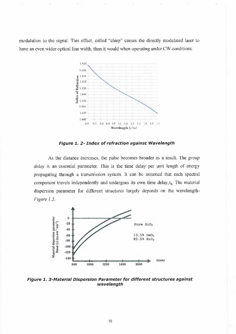
modulation to the signal. This effect, called “chirp” causes the directly modulated laser to
have an even wider optical line width, then it would when operating under CW conditions.
1 .458
1.440 -
O.fi 0 .7 0 .8 O il 1.0 11 1.2 l.:i 1.1 1.5 l.fi 1.7
Wavelength /iLl/m/
Figure 1. 2 - In d ex o f refraction against Wavelength
As the distance increases, the pulse becomes broader as a result. The group
delay is an essential parameter. This is the time delay per unit length of energy
propagating through a transmission system. It can be assumed that each spectral
component travels independently and undergoes its own time delay,xg The material
dispersion parameter for different structures largely depends on the wavelength-
Figure 1.3.
Figure 1. 3-M ateria l Dispersion Param eter for different structures againstwavelength
16

Optical fiber is composed of a core and a cladding, whose refractive indexes are
different. This difference causes the light in the core travelling at slower rate, compared to the
cladding, resulting in a spreading of the pulse [16].
1.4.2.2 Polarization mode dispersion
The fiber can be best described as an imperfect cylinder, whose physical dimensions
are not constant. The refractive index o f the optical fiber can have different values across the
horizontal and vertical axis of the core. This variation results in two orthogonal states of
polarization travelling at different speeds through the fiber-the effect is shown in Figure 1.4.
The differential phase velocity in generally goes along with a differential group velocity for
the two polarization modes [17]. This difference in group velocities broadens the pulses by
introducing a differential group delay (DGD) between the modes. The DGD per unit length
(At /L ) is called the short-length or intrinsic PMD of a fiber and is usually expressed in units
o f picoseconds per kilometer. The linear length dependence is valid only for uniformly
birefringent fibers.
Waveguide dispersion
Figure 1.4-Orthogonal polarization states travelling a t different speeds
17

1.4.2.3 Dispersion compensating methods
1. Chromatic dispersion compensation
Dispersion compensating fiber-DCF is a fiber with a refractive index profile with a dispersion
parameter of the same magnitude but opposite in sign to the transmission fiber. Opposed to
single mode fiber, which have a positive dispersion (longer wavelengths travel slower than
shorter wavelengths). DCF is made with negative dispersion over a specific range of
wavelengths [18].
2. PMD compensation
PMD becomes increasingly important as the bit rate goes higher. The fibers are
specified by their average group delay/DGD/ in ps or a mean DGD coefficient in ps / 4km :
Low PMD fiber-0.1 p s /4 k m
High PMD fiber-2 ps / 4~km
With the bit rate increasing, PMD compensation will improve the length of the fiber.
For now there are no easy and inexpensive solutions [19],
1.5 Multiplexing techniques for high capacity networks
The growth in data traffic leads to strong motivation and pressure to better utilise the
enormous bandwidth of fibre optics networks. In a basic optical communication system
comprising a transmitter, the capacity is limited by the speed at which the light can be
modulated. To overcome this limitation it is necessary to use optical multiplexing techniques
such as Wavelength Division Multiplexing and Optical Time Domain Multiplexing.
1.5.1 OTDM
Higher rate channels can be a combination o f many lower-speed signals, since very
few individual applications today utilize this high bandwidth. These lower-speed channels are
multiplexed together in time to form a higher-speed channel -Figure 1.5. This time-division
multiplexing (TDM) can be accomplished in the electrical or optical domain, with each
lower-speed channel transmitting a bit (or allocation o f bits known as a packet) in a given
18

time slot and the waiting its turn to transmit another bit (or packet) after all the other channels
have had their opportunity to transmit [20],
Figure 1. 5 - Several TDM channels with b it interleaved multiplexing
1.5.2 WDM
One obvious choice for exploiting more of the fiber’s THz bandwidth is WDM
(wavelength division multiplexing), in which several baseband-modulated channels are
transmitted along a single fiber but with each channel located at a different wavelength. Each
of N different wavelength lasers is operating at the Gbps speeds, but the aggregate system is
transmitting at N times the individual laser speed, providing a significant capacity
enhancement-F/gwre 1.6. The WDM channels are separated in wavelength to avoid cross talk
when they are (de) multiplexed by a non-ideal optical filter. The wavelengths can be
individually routed through a network or individually recovered by wavelength-selective
components. WDM allows us to use much o f the fiber bandwidth, although various device,
system, and network issues will limit the utilization o f the full fiber bandwidth [21], The
concept and components used in the design of complete WDM systems will be described in
more detail later in the thesis.
Figure 1. 6-Many WDM channels propagating in a single optical fiber
19

1.5.3 CDM
An additional multiplexing technology is code-division multiplexing (CDM). Instead
of each channel occupying a given wavelength, frequency or time slot, each channel
transmits its bits as a coded channel-specific sequence of pulses. This coded transmission
typically is accomplished by transmitting a unique time-dependent series of short pulses.
These short pulses are placed within chip times within the larger bit time. All channels, each
with a different code, can be transmitted on the same fiber and asynchronously demultiplexed
[23], One effect of coding is that the frequency bandwidth of each channel is broadbanded, or
“spread”- Figure 1.7. If ultra-short (<100 fs) optical pulses can be successfully generated and
modulated, then a significant fraction o f the fiber bandwidth can be used. Unfortunately, it is
difficult for the entire system to operate at these speeds without incurring enormous cost and
complexity.
Figure 1.7-The basic concept o f a coded pulse sequence for CDM, with each pulse located in a chip tim e and the entire code occupying a larger bit time slot
For different systems time and code division multiplexing are viewed as a favorable
way to increase the channel number. OTDM is an option for increasing the channel number
in simple fiber network structures with limited capacity. CDM techniques can be applied to
more complex network architectures since some optical CDM approaches can be realized to
support asynchronous operation of channels. Optical TDM typically can be applied to a
limited part of the network usually in the access part, whereas in the MAN part o f the
network, both WDM and CDM techniques may be implemented as shown in Figure 1.8.
20

------- »-10 nm
Figure 1.8-N etw ork combining the three different multiplexing technologies
1.6 Emerging technologies
Telecommunications is currently undergoing a large-scale transformation. Multimedia
services, HDTV and computer links are putting pressure on the telecom traffic, which will in
turn demand deploying a network that can accommodate the entire traffic in cost effective
matter. The efforts that are being made to utilize the new requirements comprise developing
of new materials, components and structure o f networks.
1.6.1 New Materials
New photonic materials are emerging with powerful properties and functionality.
Research is under way o f crystal like optical properties of synthetic materials [23] and
artificially made photonic crystals [24]. New photopolymers have displayed interesting
photonic characteristics [25]. Integration of many devices [26] requires advanced
interconnection technology of nanowires and nanodevices [27],
21

1.6.2 Components
For successfully meeting future requirements several things are essential:
1. Wide spectral range and low cost tunable components operating at high bit rates
( » 1 0 Gb/s), along with accurate wavelength converters for all optical network
with dynamic wavelength assignment [28].
2. New fibers optimized for spectrally flat and low dispersion and extended linear
behaviour, combined with dispersion compensation fibers for increase fiber span
[29],
3. Ultra high level density in a single fiber-fibers specially designed to facilitate
densely spaced channels
1.6.3 Systems and Networks
The “last-mile problem” is still present for delivering high quality broadband services.
The high cost of extending the pipes to the residential places, branch office, or small-to-
medium-sized business (SMB) has made broadband access sporadic at best. Customers were
forced to choose between DSL and cable services, and both have a record o f spotty
availability and inconsistent service. Customer interest in greater bandwidth is real. Fiber To
The Premises technology (FTTP) can easily manage lOOMbit/sec speeds, as opposed to
ADSL, which typically achieves 1.5Mbits/sec downstream [30]. FTTP makes PC backup,
telecommuting, and high-quality videoconferencing relatively simple, and can replace T1 or
T3 PBX lines for larger branch sites. For very high speed services two different architectures
have advantages.
FT TC -Fiber to the curb (FTTC) is a network technology that refers to the installation
and use of optical fiber cable directly to the curbs near homes or any business environment in
order to bring high-bandwidth services such as movies-on-demand and online multimedia
applications to the customer. Coaxial cable or another medium might carry the signals the
very short distance between the curb and the user inside the home or business [31]. Hybrid
Fiber Coax (HFC) is one example o f a distribution concept in which optical fiber is used as
the backbone medium in a given environment and coaxial cable or some other medium is
used between the backbone and individual users (such as those in a small corporation or a
22.

college environment). However there are limitations to that technology related to the inherent
bandwidth limitations o f the last mile access.
FTTH -Fiber to the home (FTTH) or Fiber to the User (FTTU) is a network
technology that deploys fiber optic cable directly to the home or business to deliver voice,
video and data services. By leveraging the extremely high bandwidth capacity o f fiber, FTTH
can deliver more bandwidth capacity than competing copper-based technologies such as
twisted pair, HFC and xDSL [32], It is considered to be completely future proof. It can
support peak speeds of 1 Gbps and can be upgraded any time to higher bandwidths by
replacing the electronics on either end of the system. The drawback of deploying a FTTH
network is the high cost per home or business passed.
1.7 Conclusions
A fully intelligent optical network would incorporate the functionality to extend
optical networks beyond point-to-point connections towards complex network architectures.
A solution for flexible network is provided by DWDM. One advantage is that it would allow
the preservation o f the existing infrastructures and architectures, seamlessly upgrading,
without disruption to existing processes. Another advantage is that it would allow different
network components within the infrastructure to be managed from the same network
management system. Just as important, the intelligent optical network enables operators to
extend DWDM transmission beyond the backbone into the access ring environment as well.
An overview o f this network and its components is provided in the next chapter.
23

References:
1. N. Savage, ‘Linking with light: high-speed optical interconnects’, IEEE Spectrum,
Volume: 39, Issue: 8, pp: 32 - 36, Aug. 2002
2. F. Louis, ‘ 10 Gbit Ethernet Over Copper: It Had to Happen’, TechView Communications
3. ‘Evolving the Network: from HFC to FTTH’, Harmonic Optical Network Solution, White
Paper
4. ‘Comparing Fiber and Copper Transmission Media’, Avocent Digital Desktops
5. ‘Enhanced Security with Fiber Optic Transmission’, Access Control and Security Systems
6. W. Gao, ‘Optoelectronic components for WDM fiber-optic communication systems and
networks’, APCC/OECC '99. Fifth Asia-Pacific Conference and Fourth Optoelectronics and
Communications Conference, Volume: 2, 18-22 Oct. 1999
7. R. Cowper, M. O ’Sullivan, G. Ribakovs, K. Roberts, ‘Perspective on the Evolution of
Next Generation High Capacity Systems’, Nortel Networks, November 1999
8., E. G. Bryant, S. F. Carter, J. V. Wright, ‘Influence of Kerr-effect on long-span optical
transmission’, IEE Colloquium on Non-Linear Effects in Fibre Communications, 20 Nov.
1990
9. S. Betti, M. Giaconi, ‘Analysis o f the cross-phase modulation effect in WDM optical
systems’, IEEE Photonics Technology Letters, Volume: 13, Issue: 1, pp: 43 - 45, Jan. 2001
10. K. Inoue, ’Experimental study on channel crosstalk due to fiber four-wave mixing around
the zero-dispersion wavelength’, Journal of Lightwave Technology,
Volume: 12, Issue: 6, June 1994
11. H. Kim, K. H. Han, Y.C. Chung, ‘Performance limitation of hybrid WDM systems due
to stimulated Raman scattering’, IEEE Photonics Technology Letters, Volume: 13, Issue:
10, Oct. 2001
12. X. P. Mao, R. W, Tkach, A. R. Chraplyvy, R. M. Jopson, R. M. Derosier,
’Stimulated Brillouin threshold dependence on fiber type and uniformity’, IEEE
Photonics Technology Letters, Volume: 4, Issue: 1, pp: 66 - 69, Jan. 1992
13. M. Eiselt; M. Shtaif, L. D. Garrett, ‘Contribution of timing jitter and amplitude distortion
to XPM system penalty in WDM systems’, IEEE Photonics Technology Letters, Volume:
11, Issue: 6, pp: 748 - 750, June 1999
24

14. A. Bogoni, L. Poti, ‘Effective channel allocation to reduce inband FWM crosstalk in
DWDM transmission systems’, IEEE Journal of Selected Topics in Quantum
Electronics, Volume: 10, Issue: 2, pp: 387 - 392, March-April 2004
15. M. Kourogi, B. Widiyatomoko, Y. Takeuchi, M. Ohtsu, ‘Limit of optical-frequency comb
generation due to material dispersion’, IEEE Journal of Quantum Electronics, Volume:
31, Issue: 12, pp: 2120 - 2126, Dec. 1995
16. A. Sugimura, K. Daikoku, N. Imoto, T. Miya, ’Wavelength dispersion characteristics of
single-mode fibers in low-loss region’, IEEE Journal of Quantum Electronics, Volume:
16. Issue: 2, pp: 215 - 225, Feb 1980
17. T. Kudou, T. Ozeki, ‘Nonlinear polarization-mode dispersion’, Conference on
Optical Fiber Communication. OFC 97, 16-21 Feb. 1997
18.High Performance Dispersion Compensating Module
Sumitomo Electric
19. A. Galtarossa, B. S. Marks, C. R. Menyuk, L. Palmieri, A. Pizzinat,
’Low-PMD fibers’, 2003 Digest of the LEOS Summer Topical Meetings,
Holey Fibers and Photonic Crystals/Polarization Mode Dispersion/Photonics
Time/Frequency Measurement and Control, 14-16 July 2003
20. S. -W. Seo, K. Bergman, P. R Prucnal, ‘Transparent optical networks with time-division
multiplexing’, IEEE Journal on Selected Areas in Communications, Volume: 14, Issue: 5, pp:
1039- 1051, June 1996
21. B. Mukherjee, ‘WDM optical communication networks: progress and challenges’ IEEE
Journal on Selected Areas in Communications, Volume: 18, Issue: 10, Oct. 2000
22. T. Pfeiffer, J. Kissing, J. -P. Elbers, B. Deppisch, M. Witte, H. Schmuck, E. Voges,
’Coarse WDM/CDM/TDM concept for optical packet transmission in metropolitan and
access networks supporting 400 channels at 2.5 Gb/s peak rate’
Journal o f Lightwave Technology, Volume: 18, Issue: 12, pp: 1928 - 1938, Dec 2000
23. P. Chavel, ‘Optical Properties of Materials: “Harnessing Light” through Novel Materials’,
Laboratoire Charles Fabry del’Institu d’Optique, Universite Paris
24. B. Temelkuran, M. Bayindir, E. Ozbay, J. P Kavanaugh, M. M. Sigalas, G. Tuttle,
’Highly doped silicon micromachined photonic crystals’, Conference on
Lasers and Electro-Optics, 2000. (CLEO 2000), 7-12 May 2000
25

25. A. Y. Mule', R. Villalaz, T. K.Gaylord, J. D. Meindl, ’Photopolymer-based diffractive
and MMI waveguide couplers’, IEEE Photonics Technology Letters, Volume: 16, Issue:
11, pp: 2490 - 2492, Nov. 2004
26. ‘Optical platform for Integration and Interconnects’, Little Optics, Inc.
27. C. M. Lieber, ‘Nanowires as building blocks for nanoelectronics and nanophotonics’,
IEEE International Electron Devices Meeting, 2003. IEDM '03 Technical Digest., pp: 12.3.1 -
12.3.3, 8-10 Dec. 2003
28. M. A. Marsan, A. Grosso, E. Leonardi, M. Mellia, A. Nucci, ‘Design of Logical
Topologies in Wavelegth Routed IP Networks’, SprintLabs
29. Lucent Technologies
30. M. Abrams, P. C. Becker, Y. Fujimoto, V. O'Byme, D. Piehler, ’FTTP Deployments in
the United States and Japan— Equipment Choices and Service Provider Imperatives’, Journal
of Lightwave Technology, Volume: 23, Issue: 1, pp: 2 3 6 -2 4 6 , Jan. 2005
31. S. -I. Aoyagi, K. -I. Sano, E. Yoneda, ’Development concept of STM-based high speed
digital FTTH systems’, Global Telecommunications Conference, 1991. GLOBECOM '91.
Countdown to the New Millennium. Featuring a Mini-Theme on: Personal Communications
32. S. -J. Park, S. Kim, K. -H . Song, J.-R. Lee, ’DWDM-based FTTC access network’,
Lightwave Technology, Journal o f , Volume: 19 , Issue: 12 , Dec. 2001
26

Chapter 2
DWDM Networks
2.1 Overview
As outlined in Chapter 1, one o f the major issues for optical systems is overcoming
the electronic bottleneck in the optical systems, which highlights the necessity of using
optical multiplexing techniques. It is possible to classify networks into three generations
depending on the physical-level technology employed. First generation networks use copper-
based or microwave technologies e.g. Ethernet, satellites etc. Second-generation networks
comprise copper links or microwave links incorporated with optical fibers. However, these
networks still perform the switching of data in the electronic domain though the transmission
of data is done in the optical domain. Finally we have the third generation networks that
employ Wavelength Division Multiplexing technology, for which the transmission and the
switching o f data is in the optical domain. This has resulted in the onset of tremendous
amount o f bandwidth availability
2.2 Dense Wavelength Division Multiplexing (DWDM)
DWDM is a technology that puts data from different sources and protocols together
on an optical fiber with each signal carried on its own separate and private light wavelength.
Using DWDM technology, up to 80 and, theoretically, more separate wavelengths o f data can
be multiplexed into a light stream transmitted on a single optical fiber. On the receiving side,
each channel is then de-multiplexed back into the original source. A basic diagram of
DWDM is shown in Figure 2.1.
DWDM is a very crucial component of optical networks that will allow the
transmission of data: voice, video-IP, ATM and SONET/SDH respectively, over the optical
layer. Hence with the development of DWDM technology, the optical layer provides the only
means for carriers to integrate the diverse technologies of their existing networks into one
physical infrastructure. For example, though a carrier might be operating both ATM and
SONET networks, with the use of DWDM it is not necessary for the ATM signal to be
multiplexed up to the SONET rate to be carried on the DWDM network. Carriers can quickly
introduce ATM or IP without having to deploy an overlay network for multiplexing [1],
27

DWDMMultiplexer
Add/DropM ux/D em ux
Receivers
\
W-Power Line Amp Amp
=1 h
Transmitters
Line R eceive Amp p reamp DWDM
DeMultiplexer
Figure 2.1-Basic DWDM configuration
2.3 Topologies
Different issues have to be addressed in the topology design of DWDM systems. The
number of nodes, maximum traffic capacity, service restoration capability, fault resiliency
and number of fiber links between the different nodes are part o f the factors that can
influence the decision of which topology to be deployed. The three main topologies will be
described, outlining the advantages and disadvantages of their implementation.
2.3.1 Point to point
This topology enables aggregate traffic with many wavelengths to be transmitted over
a single fiber, which is the most effective medium for transporting data, video, and voice
traffic, and it offers virtually unlimited bandwidth. The DWDM point-to-point architecture
shown in Figure 2.2 is inherently simple to build and troubleshoot. But the cost of running
fiber “point-to-point” to every customer location, installing active electronics at both ends of
each fiber, and managing all of the fiber connections at the central point is prohibitive [2],
Optical add/drop multiplexing is not deployed because o f the added insertion and fiber losses
resulting in degraded optical signal.
28

Node 1
Clientequipment
TrunkNode 2
Client equipment
Figure 2.2-Point to point topology in DWDM networks
2.3.2 Ring topology
As the topology is embedded in SONET/SDH ring network and its performance is
well known, it is one of the preferred. Every ring consists of optical add/drop multiplexers
(OADM) and supervisory channel shared by all nodes performing flow control and
management-F/gi/re 2.3. The ring can be dual, which feature delivers protection [3],
Bands ABC
Node 1 (hub)
Node 3Band A |
Figure 2.3-Ring topology in DWDM Networks
The hub node terminates all the DWDM channels. A channel can be provisioned to
support protected traffic between the hub node and any node in the ring. Both working and
protected traffic use the same wavelength on both sides of the ring. Protected traffic can also
29

be provisioned between any pair of optical add/drop multiplexing (OADM) nodes, except
that either the working or the protected path must be regenerated in the hub node.
2.3.3 Mesh topology
It utilizes full connectivity between different nodes- Figure 2.4. It is an ideal
compliment to the high demand for data networking and packet-based transport. While
telecommunications providers have typically built networks based on rings as a result of their
self-healing and rerouting properties, data backbones have always been mesh designs. This is
also partly a result of the complex interconnection of IP routers. Certainly, a mesh topology
shared by both IP and transport networks provide an elegant solution [4], Moreover, a mesh
with optical routing can also provide self-healing capabilities without the complexity
associated with ring software. Alternate routing through the mesh either by the router, switch,
or optical network becomes an apparent solution.
Bands ABC I t t
O l: Node 1
Band A
Figure 2.4-Mesh topology in DWDM Networks
Ring Topology vs. Mesh Topology
A ring topology is preferable owing to many of its capabilities. Unlike a mesh
network, the expense of laying out the links is reduced in the ring, because the number of
links increases only as a linear progression. The rings also have better resilience and
restoration than meshes. The ring topology besides serving as a standby link helps share the
30

load. The working segment and the protection segment o f the fiber together handle the large
data burst of the computer network. This reduces the load on the router and removes the need
for buffering [5],
2.4 DWDM Key Building Blocks
In DWDM systems, data channels must be initially multiplexed in the wavelength
domain, then transmitted through the optical network, and finally terminated at whatever
destination the information channel is being sent to. These overall systems require a large
number of electrical, opto-electronic, and optical components for correct operation. The
various functions that need to be undertaken by the numerous components in a DWDM
system include transmission, multiplexing, amplification, regeneration, and demultiplexing of
the data. These functions are performed by various components, which are described in the
following section that are used to develop a complete DWDM communication system. As a
small part o f the functions are performed in the electrical domain (laser drivers) only the
components from optical domain will be analysed,
2.4.1 Transmitters
The light source is often the most costly element of an optical communication system.
It has the following key operating characteristics: (a) peak wavelength, at which the source
emits most of its optical power, (b) spectral width, (c) output power, (d) threshold current, (e)
light vs. current linearity, (f) and a spectral emission pattern. These characteristics are key to
system performance.
There are two types of light sources in widespread use: the Laser Diode (LD) and the
Light Emitting Diode (LEDs). All semiconductor based light emitters that convert electrical
current into light operate on the principle o f the p-n semiconductor junction found in
transistors. To achieve laser action a high concentrations of electrons and holes pairs are
needed for recombination. This is achieved by high doping concentrations across the
junction,
Historically, the first achievement o f laser action in GaAs p-n junction was reported
in 1962 [6]. Both LEDs and LDs use the same key materials: Gallium Aluminum Arsenide
31

(GaAIAs) for short-wavelength devices and Indium Gallium Arsenide Phosphide (InGaAsP)
for long-wavelength devices.
The optical transmitters for DWDM systems are high resolution, precision narrow
band lasers. These lasers allow close channel spacing, which increases the number of
wavelengths that can be used in the 1500 nm band while minimizing the effects of signal
impairments such as dispersion. These lasers can use optical amplifiers that boost signal
strength for extended distances and eliminate the electronic-amplifier need to regenerate
individual optical signals. Most laser systems are designed to wavelength frequencies that
follow the standards o f International Telecommunication Union, which enables simplified
interoperability and easier component selection [7].
2.4.2 Receivers
2.4.2.1 PIN
These types o f receivers consist of an InGaAs photodiode connected to a pre
amplifier, usually fabricated with GaAs technology. InGaAs is the semiconductor material of
choice for photodiodes used in optical communications, due to its spectral characteristic. The
response of InGaAs matches the wavelength range from 1280 nm up to 1650 nm used in
optical communications. The photodiode has a bias voltage and the amplifier may have an
offset control and, additionally, a gain-control input. When it is reversed biased, its internal
impedance is almost infinite and its output current is proportional to the input optical power.
The photodiode and the amplifier can be either in different packages or they can be mounted
in the same package [8].
2.4.2.2 APD
Because the optical signal for a DWDM receiver is perturbed by nonsymmetrical
optical noise in addition to the fiber attenuation and dispersion, the input sensitivity should be
increased. The avalanche photodiode (APD) multiplies electrons via a voltage-controlled
avalanche breakdown during the conversion of photons into electrons. In order to achieve the
multiplying effect, the APD must be reverse-biased (depending on type) up to 90V. The
reverse bias for an APD must be tightly controlled to keep its multiplication factor (the gain
factor "M") constant over temperature [9]. To maintain constant gain in an APD, it can be
32

temperature-controlled with a Peltier element, or its reverse bias can be changed as a function
of temperature.
2.4.3 Modulators
2.4.3.1 Direct or External Modulation
Modulation schemes can be divided into two main categories, namely, direct or
external modulation. In direct modulation the electrical data signal (plus a dc bias current) is
applied directly to the drive current o f the laser diode to generate the optical data channel.
The main problems associated with direct modulation are that the spectral output from the
laser may be significantly broadened due to the direct modulation, and also the speed of the
laser will limit the maximum data rate that can be achieved per optical channel [10]. The
transitions of the voltage from high to low values and vice versa causes the optical
parameters of the active region to vary and so does the tuning of the resonance ability of the
cavity. Thus the optical pulse that is generated has a spectral frequency consisting of the
centre wavelength plus shorter and longer wavelengths. This effect is known as chirping
effect. In an external modulation scheme, the semiconductor laser is operating in a
Continuous-Wave (CW) mode at a fixed operating point [11]. An electrical drive signal is
applied to an optical modulator, which is external to the laser. Consequently, the applied
drive signal modulates the laser output light on and off without affecting the laser operation.
A key component in optical signal generation is thus the external modulator, which
impresses the high-speed data stream onto the optical carrier signal in TDM and WDM
applications. Some materials exhibit properties that affect at least one of the characteristics of
the light: frequency, polarization, phase or optic intensity. Such materials are used in optical
modulator devices to affect traversing light in a controllable manner. The main types of
modulators that are used are outlined below
2.4.3.2 Mach Zehnder Modulators
Optical modulator devices with speeds greater than 1 GHz are typically fabricated
from either the electro-optic crystal LiNb0 3 or III-V semiconductor compounds and multiple
quantum wells such as GaAs/AlGaAs and InGaAsP-InP, which utilize the quantum confined
Stark effect or the electro-absorption effect. Over the years, lithium niobate (LiNb03) has
33

been and continues to be the material of choice for optical modulators at bit rates of 2.5
Gbits/sec and above, primarily due to its properties of enabling low-loss waveguides and its
high electro-optic effect. LiNbC>3 travelling-wave modulators, based on a Mach-Zehnder
(MZ) waveguide structure, are the most widespread modulators in deployed systems [12],
Light wave coupled into the MZI is split equally into the two arms, each of which
may contain an active section, which converts an applied voltage into a small modification in
the propagation velocity o f light in the waveguide-F/gw'e 2.5. Over the length of the active
section(s), the velocity differences result in a phase difference in the two waves. Depending
on the relative phase o f the two waves after passing through the arms, the recombined wave
will experience an intensity modulation. By using this technique, the electrical information
applied to the modulator arms can be modulated onto an optical carrier.
Phase shifter
Figure 2.5-Schem atic for the operational principle o f MZ modulator
2.4.3.3 EA Modulators
Electroabsorption modulators are on-off devices made with InGaAsP and the percent
of absorbed photons depends on the strength of the applied filed. EAs have an almost
logarithmic attenuation of optical power that depends on a reverse voltage applied to them.
They are transparent with no voltage applied, but provided voltage is applied the absorb light
at the laser wavelength they are designed for. The electrical and optical properties of InP
enable a large number of functions to be realized in one material system. The most obvious
advantage o f using InP as an EA modulator is that the device can be made relatively small.
The bandgap energy of InP-based materials is close to the photon energies at telecoms
wavelengths, so electro-optic and electroabsorption effects can be brought into play at low
voltages and over short distances [13].
34

2.4.4 Multiplexing/ Demultiplexing
Mux/demux devices enable DWDM systems by combining (multiplexing) and
separating (demultiplexing) the different wavelength channels at the terminals. The
components require extremely high precision manufacturing techniques to route the channels
with a minimum of loss and interference with other signals. An Add/Drop Multiplexer takes a
single wavelength from a node, pulls the signal out, and allows a new signal at the same
wavelength to be inserted into the node at (roughly) the same spot. All the other wavelengths
pass through the add/drop mux with only a small loss o f power (usually a few dB). So it can
be said that precise filtering is the essential function to be performed.
Optical filters are frequently deployed in different systems to separate different
wavelengths. They perform not only functions as filtering in multiplexers and demultiplexers,
but also more complex functions as gain equalization, channel monitoring. There are many
types o f filters. Here a short description on the most important filters will be provided.
A "Bragg G rating" is a periodic or aperiodic perturbation of the effective absorption
coefficient and/or the effective refractive index of an optical waveguide. Bragg Grating can
reflect a predetermined narrow or broad range of wavelengths of light incident on the grating,
while passing all other wavelengths of the light [14], Any change to the spatial period of the
grating, or index o f refraction, will cause a proportional shift in the reflected and transmitted
spectrum. Some of the characteristics are:
• Bragg Gratings have low insertion losses and are compatible with existing optical
fibers used in telecommunication networks.
• Bragg Gratings allow low-cost manufacturing o f very high quality wavelength-
selective optical devices.
• Phase masks used to photo-imprint the Gratings allow manufacturing that is relatively
simple, flexible, low-cost and large-volume.
Some of the optical filters are interferomctrie devices that rely on the amplitude and
phase information carried by the signal and requires temporal and spatial coherence. Thus,
the characteristic length or 'size' of the components must be much smaller than the coherence
length or the signal delay time while travelling through the components must be much shorter
35

than the coherence time. In the opposite case the phase information is lost and the device
processes the intensity, rather than the amplitude of the signal.
The basic M-Z interferometer exploits the phase difference between two optical
paths. Lets consider two wavelengths are propagating through a fiber. The optical power is
then equally split and each half is coupled into two waveguides o f unequal length and then
recombined the effect will be that they will interfere constructively or destructively. Since the
refractive index of the path can be controlled and thus the effective optical path or its physical
length that means that at the recombination point different wavelengths can be selected [15].
Arrayed waveguide gratings (AWG) use silica waveguide structures to diffract light
into individual output waveguides. AWGs are often designed to optimize one o f the
performance criteria (low loss, flat top,) and do not commonly offer all three features in a
single device. For instance, to achieve a flat filter profile AWG-based MUX must insert
another element into the waveguide design that generally adds 2-3 dB of insertion loss. As
mentioned previously, AWGs use internal heaters to keep the waveguide chip at a constant
temperature-typically 75C to function properly. Heaters introduce several cost and reliability
issues. From a cost perspective, system designers using AWGs must add heater control
circuitry that introduces cost, size and complexity in the system. From reliability standpoint a
heater failure has a significant network impact since all wavelengths will be affected. Non
heated versions of AWGs are emerging, however, these devices typically have higher
insertion losses than their heated counterparts [16],
Fabry Perot Tunable Filter- FP cavity is formed in a single mode low loss
waveguide between two facets with high reflection coatings. The premise here is that the
refractive index of the waveguide can be controlled and the effective optical path between the
two mirrors also. The design involves a tradeoff between the desired free spectral range,
which sets the limit on the number o f channels that can be present if crosstalk from channels
falling in adjacent FP transmission peaks is to be avoided, and the optical phase change that
can be generated to tune the filter [17],
36

2.4.5 Amplifiers
Optical amplifiers have two great features for optical communications. They amplify
the optical signals using only optical effects, and they exhibit full scalability in terms of
communication speed and communication protocol,
2.4.5.1 Erbium-Doped Fiber Amplifiers
Erbium-doped fiber amplifiers (EDFA) use the quantum effect o f stimulated emission
into a three-level quantum system to amplify optical signals. In one quantum mechanism,
pump radiation with wavelength of 980 nm brings the Erbium atoms from the ground energy
band A to an intermediate energy band C. The atoms will stay in band C for about 10 (.is,
which is the lifetime of band C, and will leave this band through a non-radiative transition to
the metastable band B, the upper level of the amplifying transition. The lifetime of Level B is
quite long, about 10ms, which allows many Erbium atoms to be pumped into this level. The
Erbium atoms leave level B by two quantum mechanisms:
• Transitions stimulated by an optical signal in the wavelength range 1500 nm to 1580
nm that amplifies the input optical signal
• Spontaneous transitions that generate optical noise.
One of the main drawbacks of EDFA is nonlinear gain in the optical region between
1530 nm and 1560 nm, but EDFAs can achieve gain in excess of 30dB over more than 50 nm
with output powers up to 30dBm [18],
2.4.5.2 Semiconductor optical Amplifier
Semiconductor fiber optical amplifiers have been developed to serve not only as
switching elements and nonlinear elements for optical signal processing systems, but also as
in-line optical amplifiers for DWDM metropolitan transmission systems. SOA functions in a
similar way to a basic laser. The same gain mechanism is used as in laser diodes but out of
oscillation regime. The structure is much the same, with two specially designed slabs of
semiconductor material on top o f each other, with another material in between them forming
the 'active layer’: the active layer is sandwiched between a “p” region and “n” region. An
electrical current is set running through the device in order to excite electrons, which can then
37

fall back to the non-excited ground state. The recombination of electron-hole pairs generates
more photons of the same wavelength as the optical signal and hence optical amplification is
achieved [19], The most important characteristics of the SOAs are as follows;
1. High gain (25-30dB)
2. Wide bandwidth
3. SOAs are made with InGaAsP, which makes them small, compact and easily
integrable with other semiconductor components
4. Polarization dependency
5. Strong optical nonlinearity of the active gain medium which gives rise to some
suitable performances as frequency transformation and multiplication but also
to some parasitic effects as crosstalk
6. When the amplified optical signal is modulated in the gigabit per second range
and SOA operates in gain saturated regime it gives rise saturation pattern
effect.
SOA can be classified into two groups, Fabry-Perot Amplifiers (FPA) and Travelling
Wave Amplifiers (TWA). The difference is the reflectivity coefficient value of both mirror
surfaces.
2.5 Optical Switching
The most deployed network for transmitting Internet data is DWDM systems that
carry 32-80 wavelengths modulated at 2.5Gb/s and/or 10 Gb/s per wavelength. Most
networking equipment today is still based on electronic-signals, meaning that the optical
signals have to be converted to electrical ones, to be amplified, regenerated or switched, and
then reconverted to optical signals. This is generally referred to as an 'optical-to-electronic-to-
optical' (OEO) conversion and is a significant bottleneck in transmission [20], Huge amounts
o f information travelling around an optical network needs to be switched through various
points known as nodes. Information arriving at a node will be forwarded on towards its final
destination via the best possible path, which may be determined by such factors as distance,
cost, and the reliability of specific routes. The conventional way to switch the information is
to detect the light from the input optical fibers, convert it to an electrical signal, and then
convert that back to a laser light signal, which is then sent down the fiber you want the
information to go back out on.
38

The basic idea of Optical Switching is that by replacing existing electronic network
switches with optical ones, the need for OEO conversions is removed. Clearly, the
advantages of being able to avoid the OEO conversion stage are significant. Optical
switching has long been proposed as a faster, less expensive, and more efficient alternative to
electronic switching [21],
2.5.1 Optical Burst Switching
A potential disadvantage of optical circuit switching is that, once a wavelength has
been assigned, it is used exclusively by the allocated source. If 100 percent of its capacity is
not in use for 100 percent of the time, then clearly there is inefficiency in the network. One
solution to this problem is to allocate the wavelength for the duration of the data burst being
sent.
Optical burst switching is based on the separation of the control plane and the data
plane. In optical burst switching data packets are aggregated into much larger bursts before
transmission through the network. The burst is preceded in time by a control packet, which is
sent on a separate control wavelength and requests resource allocation at each switch. When
the control packet arrives at a core cross-connect (or switch) capacity is reserved in the cross-
connect for the burst. If the required capacity can be reserved the burst can pass through the
cross connect [22], The burst has to be buffered by the OEO edge device while the
wavelength is being set up, so the signalling has to be very fast.
The data plane is “service transparent.” The control plane can operate at a much lower
data rate, but must follow the path o f the data plane (e.g. use optical supervisory channel).
There are lots o f difficulties related to OBS such as creating a robust but simple out of
band signalling system. But the benefits are very clear. By holding the label switched path
(LSP) open only for the duration o f the burst, we achieve a statistical multiplexing o f the
wavelength in the time domain. This should increase the efficiency o f backbone utilization
dramatically when compared to optical circuit switching.
39

2.5.2 Optical Packet Switching
An Optical Packet Switch (OPS) is the true, optical equivalent o f an electronic packet
switch involving reading an embedded label and making a switching decision using this
information. It uses in band control information; the header follows the rest of the packet
loosely, so there cannot be any reservation of resources. Reading and reinserting of packet
headers with strict timing requirements are needed, due to the short packet duration-typically
around 1 j_l s .
A key issue in OPS is whether to use synchronous or asynchronous transmission; the
latter enables the use of variable length packets providing a close analogy to electronic IP
packets. Asynchronous operation removes the requirement for synchronisers at the switch
input, which can be costly to implement, however it is more demanding in terms of buffer
control and utilisation. The implementation of OPS requires a packet labelling technique
suitable to optical systems. Various schemes have been proposed and demonstrated, most of
an opto-electronic nature, i.e. use optical detection and electronic processing rather than all
optical processing. The optical packet switch must incorporate a number of functions, for
example, label swapping, contention resolution and payload switching are key requirements;
together with appropriate algorithms for scheduling packets through the switch [23].
A major advantage of optical packet switching lies in its bandwidth efficiency and
ability to support diverse services, hence research is now growing on bringing the packet
switching concept into the optical domain, that is optical packet switching. Until now work
on this subject has focused on the synchronous container approach to networking. However,
given the increasing dominance o f the IP client signal, which presents variable packet lengths
to the optical network, it is clear that the synchronous fixed length container approach may
not be optimum.
Although current routers offer significant advancements over previous generations,
they still cannot scale sufficiently to meet projected traffic demands, nor do they provide the
very high level of availability required to run mission-critical traffic over IP networks. In
addition, electrical switch fabrics have posed physical limitations that prevent routers from
scaling sufficiently to avoid premature forklift upgrades.
40

All of this points to the need for a new kind of scalable router architecture that routes
IP/MPLS packets electronically, but switches them optically. This combination of large port
count with high speed switching (nanoseconds) is needed realize this next generation IP
routing platform.
2.5.2.1 MPLS Overview
In traditional IP based networks, carriers use one IP network for data and a separate
circuit-switched network for voice, but that distinction is increasingly breaking down.
Routers work independently to determine the best next hop for packet forwarding. Robust
interior gateway protocols consult a link state database to understand the entire network
topology and choose the best next hop based on the lowest cost. As demand for "converged"
network applications grows, carriers and corporations are eager to bridge the gap between
diverse technologies to provide a seamless backend capable of supporting all of the latest
applications and services. Ultimately, all lowest equal cost paths are selected and used to
forward data [24], The premise of multiprotocol label switching (MPLS) is to speed up
packet forwarding and provide for traffic engineering in Internet protocol (IP) networks.
MPLS alleviates many of the problems that arise in shifting applications that have
traditionally run on circuit-switched networks to IP-based networks, such as the Internet.
Because MPLS can handle any type o f traffic, carriers can use it in their core infrastructure to
converge traffic from all of its networks onto a single network, saving money in operational
costs. To accomplish this, the connectionless operation o f IP networks becomes more like a
connection-oriented network where the path between the source and the destination is
precalculated based on user specifics. To speed up the forwarding scheme, an MPLS device
uses labels rather than address matching to determine the next hop for a received packet.
Among the many positive attributes MPLS brings to internetworking is the ability to provide
connection-oriented services to the inherently connectionless IP networks. The label
switched path, or LSP, is the establishment of a unidirectional end-to-end path forwarding
data based on fixed size labels.
2.5.2.2 Generalized MPLS (GMPLS)
GMPLS extends MPLS to provide the control plane (signalling and routing) for
devices that switch in any of these domains: packet, time, wavelength, and fiber. This
41
common control plane promises to simplify network operation and management by
automating end-to-end provisioning of connections, managing network resources, and
providing the level of QoS that is expected in the new, sophisticated applications.
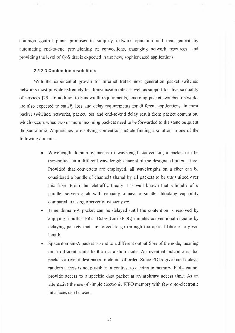
2.5.2.3 Contention resolutions
With the exponential growth for Internet traffic next generation packet switched
networks must provide extremely fast transmission rates as well as support for diverse quality
of services [25], In addition to bandwidth requirements, emerging packet switched networks
are also expected to satisfy loss and delay requirements for different applications. In most
packet switched networks, packet loss and end-to-end delay result from packet contention,
which occurs when two or more incoming packets need to be forwarded to the same output at
the same time. Approaches to resolving contention include finding a solution in one of the
following domains:
• Wavelength domain-by means o f wavelength conversion, a packet can be
transmitted on a different wavelength channel of the designated output fibre.
Provided that converters are employed, all wavelengths on a fiber can be
considered a bundle of channels shared by all packets to be transmitted over
this fibre. From the teletraffic theory it is well known that a bundle of n
parallel servers each with capacity c have a smaller blocking capability
compared to a single server of capacity nc.
• Time domain-A packet can be delayed until the contention is resolved by
applying a buffer. Fiber Delay Line (FDL) imitates conventional queuing by
delaying packets that are forced to go through the optical fibre o f a given
length.
• Space domain-A packet is send to a different output fibre o f the node, meaning
on a different route to the destination node. An eventual outcome is that
packets arrive at destination node out of order. Since FDLs give fixed delays,
random access is not possible: in contrast to electronic memory, FDLs cannot
provide access to a specific data packet at an arbitrary access time. As an
alternative the use o f simple electronic FIFO memory with few opto-electronic
interfaces can be used.
42

2.6 Conclusion
Until now the technical obstacles to achieving an all-optical network were posing a
problem. The fundamental issue was the inability to switch. Packet switching at gigabit
speeds seemed impossible. Implementing more efficient bandwidth utilization in WDM
networks by employing wavelength packet switching architectures is essential. In these
networks, WDM optical packets are generated using fast tunable Sight sources, and then
routed to specific nodes in the optical network by using optical filtering techniques. In the
next chapter the different tuning mechanism and structures for the tunable light sources will
be described in details.
43

References:
1. S. Song, Z. Wu, ’A broadband integrated services network architecture based on DWDM’,
Canadian Conference on Electrical and Computer Engineering 2001, Volume: 1, 13-16 May
2001
2. A. Aloisio, F. Cevenini, V. Izzo, ’An approach to DWDM for real-time applications’,
IEEE Transactions on Nuclear Science, Volume: 51, Issue: 3, pp: 526 - 531, June 2004
3. D. Stoll, P. Leisching, H. Bock, A. Richter, ’Metropolitan DWDM: a dynamically
configurable ring for the KomNet field trial in Berlin’, IEEE Communications
Magazine, Volume: 39, Issue: 2, Feb. 2001
4.DWDM in Metropolitan Area Networks, Cisco
5. B. Buescher, ‘Benefits of Metropolitan Mesh Optical Network’, Tellabs Optical
Networking Group
6. S. Forrest, P. Deimel, J. -Y. Glacet, R. Logan, ’Narrow spectral width surface emitting
LED for long wavelength multiplexing applications5, IEEE Journal of Quantum
Electronics, Volume: 20, Issue: 8, pp: 906 - 912, Aug 1984
7. H. Kobrinski, M. P. Vecchi, M. S. Goodman, E. L. Goldstein, T. E. Chapuran, J. M.
Cooper, M. Tur, C. —E. Zah, ‘Fast wavelength-switching o f laser transmitters and amplifiers’,
IEEE Journal on Selected Areas in Communications, Volume: 8 , Issue: 6, pp: 1190 - 1202,
Aug. 1990
8. D. Wake, T. P. Spooner, S. D. Perrin, I. D. Henning, ’50 GHz InGaAs edge-coupled PIN
photodetector’, Electronics Letters, Volume: 27, Issue: 12, pp: 1073 - 1075,6 June 1991
9. K. K. Loi, M. Itzler, ‘Avalanche Photodetectors for lOGb/s Fiber Optic Receivers’, JDS
Uniphase Corporation, EPITAXX Division
44

10. J. A. MacDonald, E. I. Ackerman, J. L Prince, ’Signal and noise analysis of direct
modulation fiber optic link with optical component and arbitrary lossless matching circuits’,
IEEE MTT-S International Microwave Symposium Digest, 1994.,23-27 May 1994
11. E. I. Ackerman, J. L. Prince, J. A. MacDonald, ’Signal and noise analysis of external
modulation fiber optic link with optical component and arbitrary lossless matching circuits’,
IEEE MTT-S International Microwave Symposium Digest, 1995., 16-20 May 1995
12. Y. Kisaka, A Tomizawa, A. Hirano, S. Kuwahara, Y. Miyamoto, ’Compact-spectrum RZ
signal generated by single-stage push-pull type Mach-Zehnder modulator for DWDM
transmission’, Electronics Letters, Volume: 39, Issue: 3, pp: 304 - 306,6 Feb. 2003
13. D.G.Moodie, M.J. Harlow, M.J. Guy, S.D. Perrin, C. W. Ford, M.J.Robertson,
’Discrete electroabsorption modulators with enhanced modulation depth’, Journal of
Lightwave Technology, Volume: 14, Issue: 9, pp: 2035 - 2043, Sept. 1996
14. R. Zengerle, O.Leminger, ’Phase-shifted Bragg-grating filters with improved
transmission characteristics’, Journal o f Lightwave Technology, Volume: 13, Issue: 12, pp:
2354-2358 , Dec. 1995
15. K.Tsuzuki , H. Takeuchi, S. Oku, M. Tanobe, Y. Kadota, F. Kano, H. Ishii, M.
Yamamoto, ‘InP-based monolithic optical frequency discriminator module for WDM
systems’, IEICE TRANSACTIONS ON COMMUNICATIONS
16. K. Takada, M. Abe, T. Shibata, K. Okamoto, ’10-GHz-spaced 1010-channel tandem
AWG filter consisting of one primary and ten secondary AWGs’, IEEE
Photonics Technology Letters, Volume: 13, Issue: 6, pp: 577 - 578, June 2001
17. H.K.Tsang, M.W.K. Mak, L.Y. Chan, J.B.D. Soole, C. Youtsey, I. Adesida,
’Etched cavity InGaAsP-InP waveguide Fabry-Perot filter tunable by current injection’,
Journal of Lightwave Technology, Volume: 17, Issue: 10, pp: 1890- 1895, Oct. 1999
45

18. S. Novak, A. Moesle, ‘Analytic model for gain modulation in EDFAs’,
Journal of Lightwave Technology, Volume: 20, Issue: 6, pp: 975 - 985, June 2002
19. S. Kitamura, N. Kimura, K. Kurata, M. Yamaguchi, ’Low-switching-current SOA gate
module with wide optical input dynamic range’, 22nd European Conference on Optical
Communication, 1996. ECOC '96.Volume: 3, 15-19 Sept. 1996
20. R. Medina, ‘Photons vs. electrons [all optical network]’, IEEE Potentials, Volume:
21. Issue: 2, pp: 9 - 11, April-May 2002
21. Optical Phased Array Technology for High Speed Switching, Whitepaper, Chiaro
22. S. Sheeshia, Y. Chen; V. Anand, Ch. Qiao, ’Performance comparison of OBS and
SONET in metropolitan ring networks’, IEEE Journal on Selected Areas in Communications,
Volume: 22, Issue: 8, pp: 1474 - 1482, Oct. 2004
23. C. Develder, A. Stavdas, A. Bianco, D. Careglio, H. Lnsethagen, J. P. F. -P . Gimenez,
V. Caenegem, S. Sygletos, F. Neri, J. Sole-Pareta, M. Pickavet, L. Sauze, N ; P. Demeester,
’Benchmarking and viability assessment of optical packet switching for metro networks’,
Lightwave Technology, Journal of, Volume: 22, Issue: 11, pp: 2435 - 2451, Nov. 2004
24. J. Yu; G. -K. Chang; A. Chowdhury, J. L. Long, ’Spectral efficient DWDM optical
label/payload generation and transport for next-generation Internet’,
Journal of Lightwave Technology, Volume: 22, Issue: 11, pp: 2469 - 2482, Nov. 2004
25. S. Bjornstad, M. Nord, D.R. Hjelme, N. Stol, C. Develder, J. Cheyns, E. V. Breusegem,
E. Baert, D. Colle, M. Pickavet, P. Demeester, F. Callegati, ‘Optical burst and packet
switching: node and network design, contention resolution and quality o f service’,
Proceedings of the 7th International Conference on Telecommunications, 2003. ConTEL
2003., Volume: 2, pp: 775 - 782,11-13 June 2003
46

Chapter 3
Tunable Lasers
3.1 Overview
To meet the ever increasing traffic demands of cities and regions, metro network
operators are turning to the same optical networking technologies that have relieved
bottlenecks in core or long-haul networks. However, metro traffic is far less predictable than
long-haul traffic: The traffic mix changes constantly as subscribers are added and removed,
services are expanded, and providers scale up their bandwidth. DWDM systems promise to
relieve metro providers, but extra channel capacity is only part o f the solution. To deliver all
the metro provisioning capacity that is promised with the flexibility to use it as market needs
demand, vendors are now exploring the use of tunable lasers. In contrast to fixed-wavelength
lasers, tunable lasers can tune to many different operational wavelengths, rather than just one.
Metro carriers can substantially increase their DWDM systems' virtual channel capacity at
initial deployment by using tunable lasers. Many DWDM systems featuring tunable optics
are the ultimate choice.
3.2 Applications of Tunable Lasers
3.2.1 Network planning
Instead of the burdening process of forecasting lasers on a wavelength-by-wavelength
basis optical networking companies can now reduce the amount of intricacy thanks to the
advent of tunable technology. The expected outcome of this application is that there is an
ease o f forecasting and planning and last minute changes can be more easily accommodated
resulting in fewer lost revenue opportunities [1].
3.2.2 Inventory reduction
In order to accommodate fluctuating demands the telecom operators needed to supply
more units from the fixed wavelength sources resulting into huge expenses. Tunable lasers
essentially remove the need to stock inventory at such massive levels. The new technology
proves to be efficient for the vendors as well: vendors eventually need to manufacture a
reduced number of part codes, which simplifies the process [2],
47

3.2.3 Sparing
Tunable lasers can be deployed in the event of a fixed wavelength laser failure. Thus
instead of keeping an additional fixed wavelength laser to replace the already deployed one,
tunable technology is used. This reduces the necessary planning, as there is a wide range of
tunability. One tunable laser can easily substitute any of the transmitters [3],
3.2.4 Re-configurable Optical Add/Drop Multiplexer (R-OADM)
To date, deployment of Optical Add/Drop Multiplexers (OADM) has been somewhat
hampered, either by the lack o f flexibility offered by commercial solutions, or by the cost
premium demanded for offering flexibility. There are many ways that a re-configurable
OADM can be implemented - from a tunable filter approach to a back-to-back multiplexer
with a switching fabric between. In either case the application demands tunable lasers. The
benefit offered by a R-OADM is the ability to change the capacity being dropped and
inserted at a remote site without the need for an expensive bandwidth manager. This results in
major savings for the network provider. The impact of tunable lasers on this application is in
the resolution of blocking scenarios without the need for a full complement of transponders.
These savings mean that there is reduced price sensitivity for the tunable laser component in
this case [4, 5],
3.2.5 Photonic cross connects
The function of the cross connection can be implemented using a photonic switch
surrounded by transponders, the transponders are wavelength converters used to overcome
wavelength blocking and provide SONET like performance monitoring. Most high-speed
networking equipment uses multimode or single mode fiber optic interfaces, where the data is
carried at 850nm, 1310nm or 1550nm. Since WDM systems need to multiplex different
wavelengths together, these signals must all be converted to a particular wavelength that is
suitable. If the photonic switch resides at a point in the network where two metro rings meet,
tunable lasers can be used to enable traffic to transfer between rings without crossing an
electrical switch [5].
48

3.2.6 Fast Packet Switching
One key feature of a solid-state tunable laser is that it can be switched from one
wavelength to another is a few nano-seconds (ns). This enables wavelength switching at the
packet level, which can then be used to route data traffic based on colour through a passive
router such as a N x N arrayed waveguide grating (AWG) [6],
3.2.7 Wavelength converters
All optical wavelength converter devices capable of converting high-speed data rates
are essential elements in DWDM networks. The ability of the wavelengths to be shifted leads
to an efficient and easily managed network. One of the techniques used is an optically
injected semiconductor tunable laser, where the laser oscillation is intensity modulated by the
injection light with another wavelength. The data signal is transferred from the injection
wavelength light to the laser oscillation wavelength.
From all the applications discussed above it is clear that tunable lasers are the future
o f optical networks not only from manufacturer’s perspective. Given the variety o f
applications with differing needs, no tunable-laser technology is optimized for all of these
DWDM requirements. The choice o f laser technology will be determined by many factors,
including output power, line width, relative intensity noise (RIN), tuning range, tuning time,
and stability. It is important to understand the relative strengths and weaknesses of the
different tunable-laser technologies against these requirements when considering what type of
laser to implement for a given optical-network application [7].
Tunable lasers can be produced using a variety of laser structures, each with its own
advantages and disadvantages. Five o f the main basic laser structures are distributed feedback
(DFB), distributed Bragg reflector (DBR), vertical-cavity surface-emitting laser (YCSEL),
and extemal-cavity lasers (ECL), sampled-grating DBR (SGDBR)
These different laser structures use different tuning mechanism that partially or fully
covers DWDM band. The categories in which those mechanisms can be divided are actually
three:
49

3.3 Thermal tuning
3.3.1 DFB
DFB lasers are simple structures that work by using an internal grating to change the
wavelength of operation. The combination o f its refractive index and the spacing of the
corrugations serves to reflect only a specific wavelength of light. In this way the corrugations
act as a grating, reflecting only a specific wavelength back into the cavity but allowing others
to pass through. The desired wavelength is fed back into the cavity, and this is taking place
over the whole length of the laser. The only laser light that builds up within the active layer is
light o f this specific wavelength, and so that is the only wavelength emitted from the laser.
DFBs are tuned to Inter national Telecommunication Union (ITU) grid wavelengths by
changing the temperature of the medium, either through drive-current changes or a
temperature-controlled heat sink, which changes the refractive index of the internal
waveguide. The thermally induced wavelength switching is slow (typically < 0.5nm/s) that is
the reason other types are preferred for deployment in DWDM networks. However extremely
large mode hop free tuning ranges can be attained. The thermal tuning rate of the lasers
amounts to 25-30 GHz/K (0.06 nm/K). DFB lasers use a thermo-electric cooler (TEC) to
maintain wavelength accuracy. Changing the temperature of the DFB laser changes the
wavelength. By taking advantage of this feature, with improvements in thermo-electric
coolers, the temperature can be precisely controlled to produce a stable, well-defined output
wavelength with an acceptable line width. In general, DFB lasers are well behaved and
characterized and have proven reliable [8],
While DFBs offer some manufacturing, performance, and operational advantages,
they have the disadvantages of low output power and very limited tuning range. Their
effective tuning range tends to be limited because, as the tuning temperature increases, the
efficiency and output power of the device decreases.
To extend the tuning range, these devices can be integrated into ensemble or side-by-side
laser arrays o f several lasers on one chip coupled into a single output as shown in Figure 3.1.
One laser at a time is driven to select a wavelength [9,10],
50

There are, however, some limitations even to this design. This solution is not
continuously tunable, the combining mechanism is optically inefficient, and the chip size
leads to yield issues.
3.4 Mechanical and Micro Electrical Mechanisms
3.4.1 VCSEL
Conventional lasers are known as “edge emitters” because their laser light comes out
from the edges. Also, their laser cavities run horizontally along their length. A vertical cavity
surface-emitting laser, however, gives out laser light from its surface and has a laser cavity
that is vertical. A typical VCSEL consists o f an active region sandwiched between two
oppositely doped distributed Bragg reflectors (DBRs) that form the optical cavity- in a
VCSEL there are several layers of partially reflective mirrors above and below the active
layer. Layers of semiconductor with differing compositions create these mirrors, and each
mirror reflects a narrow range o f wavelengths back into the cavity in order to cause light
emission at just one wavelength. VCSELs have several advantages over edge-emitting lasers.
A device generally supports a single Fabry-Perot (FP) wavelength within the gain spectrum,
so the FP wavelength, and not the gain peak, determines the lasing wavelength. By changing
the thickness of the optical cavity, it is possible to change the FP wavelength supported by
the cavity. In other words, changing the thickness of the optical cavity changes the lasing
wavelength of the device [11],
1 The figure is taken from “Tunable lasers”, Bruce E,
51

By integrating the top DBR of a VCSEL with a micro-electro-mechanical-systems
(MEMS) cantilever, it is possible to precisely change the cavity thickness to achieve an
electrically tunable device-see Figure 3.2. To tune the device, a reverse bias voltage is
applied across the air gap between the top n-DBR and p-DBR. The resultant electrostatic
force pulls the cantilever down toward the substrate, shortening the air gap to tune the laser
output to a shorter wavelength. Because the movement is elastic, there is no hysteresis in the
wavelength-tuning curve; when the voltage is removed, the cantilever returns to its original
position. A simple and efficient process allows to monolithically integrate a high
performance VCSEL with a micro-electro-mechanical system (MEMS) tuning structure that
can be electrostatically activated at very low tuning voltage using standard low cost
electronics [12,13],
MEMS mirror
VCSEL
2Figure 3.2-VCSEL with MEMS Tuning Structure
VCSEL lasers can be thermally tuned as well. The process of thermal tuning is slow
and the range is limited. The speed depends on how quickly heat can be supplied and
removed from the active region. For VCSELs this is an issue because their “pillar” structure
leads to high thermal resistance. Some experiments show achieving lO.lnm by heating the
active region.
VCSELs are also more efficient than edge emitters and give out more light for the
same electric current applied to them (they have a lower “threshold current”). Additionally,
the light beam from VCSELs is narrower and more circular, making it easier to get the light
into an optical fiber. Low-power VCSELs at 850nm are widely used for short-distance
2 The figure is taken from “Tunable lasers”, Bruce E.
52

networks, but high-power 1550nm products will be needed for widespread use in large-scale
optical networks. Wavelength switching times o f under 2 (.is have been reported [14], [15].
Optimization o f the mechanical design are being analyzed which can subsequently reduce the
switching time.
3.4.2 ECL
External Cavity Lasers (ECL) uses a resonant cavity external to the active
semiconductor section, which is typically a simple Fabry-Perot gain chip. ECLs provide high
power, large tuning range, and narrow linewidth with high stability and low noise. The
external-cavity approach alters the beam wavelength by mechanically adjusting the laser
cavity, rather than through current or temperature changes applied to a semiconductor
material, which causes delay in wavelength switching and prevents them from being used in
fast packet switched networks. Furthermore, they provide continuous tuning through the
entire spectrum of the gain medium, where other common laser technologies (like DBRs)
exhibit mode hops between stable points in the spectrum. This laser consists of a separately
fabricated gain medium (a simple Fabry-Perot laser diode) and an external cavity formed of
separately fabricated optical structures (a diffraction grating and mirror) integrated at an
assembly step. Generally the design o f the ECL is based either on Littman-Metcalf or Littrow
cavities.
3Figure 3.3-ECL based on Littman Cavity
3 The figure is taken from “Tunable lasers”, Bruce E.
53

The Littman cavity, Figure 3.3, uses a grating and tuning mirror in a patented
configuration to deliver the highest level o f side mode suppression (typically 60dB) with
narrow linewidth (0.3-5MHz) [16].
Figure 3.4-ECL based on Littrow Cavity
The Littrow cavity, Figure 3.4, simply uses a grating to deliver substantial increases in
output power at the slight reduction in sidemode suppression (40dB) [17].
In an ECL tunable-laser design, some portion of the laser cavity resides off the laser
chip, and the diode acts as a gain medium only. In some ECL source lasers, one facet of the
laser diode is coated to act as a high reflector while the laser output and cavity tuning are
provided on the other side of the chip.
Littman-Metcalf and Littrow cavity configurations are examples of such single-sided
ECL sources in which gratings are used to provide optical feedback and tune wavelength. In a
double-ended ECL (Figure 3.5) configuration one facet of the laser diode-uncoated or coated
to be a partial reflector-acts as an output coupler. Light transmitted from the output-coupling
facet is collimated, passed through a Faraday isolator, and focused into an output fiber [18].
54

c
4Figure 3. 5-Double Ended ECL Configuration
Recent technological advances have brought ECLs to the forefront of optical-
networking component technology. In particular, the application of MEMS to optical-
component designs produces high-performance micro-optics that readily fit on standard
transmitter cards and can be manufactured at competitive costs in the optical-networking
industry.
3.5 Electronic Wavelength tuning
Most continuously tunable lasers exploit the electronic refractive index change
induced by the free carrier plasma effect for the tuning of the emission wavelength. Generally
a p-I-n type double heterostructure junctions form a waveguide, where carriers are injected
into the intrinsic region. However with increasing the current the recombination rate is also
increased therefore, the excess carrier density saturates at high injection. The change of the
refractive index is usually caused by injection of free carriers or by increasing the
temperature or combination o f both. The former leads to a decrease of the refractive index
and thus to a decrease o f the emission wavelength (blue shift), while the latter leads to a red
shift and is usually unintentional. Here a Bragg grating reflectors are used such that the
reflection spectrum represents a comb of peaks.
3.5.1 GCSR
Grating Assisted Codirectional Coupler with Sampled Reflector /GCSR/ lasers consist
of four sections. The front one is a gain block, followed by a phase module used for fine-
tuning the wavelength. Between the gain section and the phase section is the grating assisted
codirectional coupler, which acts as a course tuner. GACC uses grating assisted wavelength
4 The figure is taken from “Tunable lasers”, Bruce E
E x ternal
T u n in g Device
Fiber
F ocusing Lens
Polarization
P reserv in g Fiber
D iode
O u tp u t
C ollim ating Lens
Iso la to rG ain C hip
55

selective coupling between two forward propagating channel modes of directional coupler
made of two parallel waveguides. As the waveguides are not synchronized /each one supports
an optical mode with a different phase velocity/ those two modes can only couple energy
with the assistance o f the grating which provides the necessary phase matching [19,20],
The structure of GCSR incorporates two waveguides -one that runs forward to the
phase module and gain block, and another one, at a higher level, that runs backward into the
last section, which is the Bragg grating-Figure 3.6.
Gain GACC Phase Rear Mirror
5Figure 3.6-GCSR Structure
In this laser most of the light comes straight from the gain block out the front of the
laser, to be sourced into a fiber. There is a small amount of reflected light at the front of the
laser back into the laser and this will be bounced of the Bragg grating at the back of the laser
if it is o f the correct frequency, amplified by the gain section, and emitted from the front of
the laser. Some of this is reflected back into the laser as before and the whole process can be
repeated again and again.
The combination of the sampled reflector section and the codirectional coupler
section ensures lasing at only one cavity mode providing wavelength selective loss. The
reflection peaks of the sampled reflector are about 4 nm apart. The coupler acts as a filter
with about 8 nm bandwidth. The wavelength tuning is a response to the tuning signals. When
those signals are changed, the carrier concentrations in each section change until it reaches
the steady state value of the new operating point. During the tuning process the laser may hop
5 The figure is taken from “Tunable Semiconductor Lasers”, Coldren L. A.
56

between different peaks of the sampled reflector and different longitudinal cavity modes,
which have spacing of usually 0.2 nm. During these transitions the laser frequency changes
abruptly and large power variations occur. GCSR lasers are the first devices to reach
commercialization after the development of the simple DBR laser. The tunability they
provide is in the nanosecond range. It can be influenced depending on the switching
technique that is being used. The usage of pre-distortion differentiated pulses drives the
switching time down [21 ].
3.5.2 SG-DBR/SSG-DBR lasers
SG-DBR tunable lasers use-grating reflectors at either end o f the cavity to produce a
spectral comb response-F/g-wre 3.7. The back and front sampled gratings have slightly
different pitch so the resulting spectral combs have slightly different mode spacing. Tuning to
a specific wavelength is achieved by controlling the current in the two grating sections so as
to align the two combs at the chosen wavelength. The laser, therefore, "hops" between
wavelengths. An additional contact is normally required to adjust the phase so an integral
number of half-wavelengths exists. If this phase adjustment is not included, then mode
stability can suffer and noise can increase [22], While these types of lasers offer a wide
tuning range, they suffer from low output power and broad line width. Furthermore, they
have complex drive requirements when compared to other laser designs. They have more
electrodes, and accurate wavelength selection requires matching of numerous input currents
with the appropriate electrodes. Sampled gratings with grating-assisted co-directional coupler
filters add a filter to select one of the sampled-grating peaks, making it easier and cleaner to
select a wavelength but at the cost of additional manufacturing complexity. SG-DBRs also
suffer from low output power, which can potentially be recovered with a semiconductor
optical amplifier (SOA) [23]. However, SOAs are noisy devices and can cause other
perturbations that will prevent them from meeting requirements of RIN and line width for 10-
Gbit/sec narrow-wavelength-spacing extended-reach applications. Because SG-DBR devices
are grown on indium phosphide wafers, the ability of the SG-DBR laser designs to meet all
system noise, power, and tuning range requirements are limited to the physical characteristics
that can be achieved by a single semiconductor system. In short, with all monolithic growth
approaches, tradeoffs must be made between the material gain characteristics, electro-optical
coefficients, and DBR current-tuning efficiencies. These devices can switch wavelength in
57

nanoseconds. The SSG-DBR lasers add more complexity to the fabrication o f the sampled
gratings, which results in lower output power compared to SG-DBR at around tmW, but at
the same time have improved tuning range because o f the phase modulated sampled gratings
[24], They also switch in the nanosecond region. The design of SSG-DBR lasers differs only
in the design of the mirrors: the gratings in the mirrors are periodically chirped instead of
sampled. The advantage of this approach is that the grating occupied the entire length of the
mirror so that a much higher reflection can be achieved with a lower coupling constant in the
grating. The other main advantage is that the reflectivity of the individual peaks can be
tailored such that all the reflection peaks have the same magnitude.
Front Mirror Gain Phase Rear Mirror
ΗJiiii a m m i m i I i n in m i m i m i
SG-DBR6Figure 3.7-Schematic diagram of SG-DBR laser structure
While DWDM systems make the most o f a network's configuration by carrying
multiple channels along a single strand of fiber, the amount of supporting components
needed-and the complexity o f organizing them-almost diminishes the efficiency this
technology is supposed to bring to telecom networks. Tunability eases quite a bit of this
complexity by significantly reducing the number of necessary components in DWDM
systems, making it an excellent facilitator for optical add/drop multiplexers (ADMs) and
optical switching/routing. Tunability enables faster and more flexible network
reconfiguration, which is one of the greater challenges to carriers, as their ability to meet
customers' demands for effective bandwidth management is caicial to success in marketplace
6 The figure is taken from “Tunable Semiconductor Lasers”, Coldren L. A.
58

References:
1. Intel Tunable Laser Technology
2. R. Simes, G. Fish, P. Abraham, Y. Akulova, M. Larson, ‘InP chip scale integration
platform for high-performance tunable lasers’
3. E. Bruce, ‘Tunable lasers’, IEEE Spectrum, Volume: 39, Issue: 2, pp: 35 - 39, Feb. 2002
4. D. Wang, Y. Shao, Q. Shao, ‘Reconfigurable optical add drop multiplexer (R-OADM): key
network element for reconfigurable optical network’, Oplink Communications, Inc. (USA)
5. Dr. D. Arent (Network Photonics), A. Marin (Agility Communications), ‘Third Generation
DWDM Networks Near Reality’, Lightwave-March 2001
6. A. Rafael (Texact Technologies), M. Ogazi, R.I. Killey (University College London),
‘Routes Towards Enabling Optical Packet Networks’
7. M. L. Masanovic, V. Lai, J. S. Barton, E, J. Skogen, L. A. Coldren, D. J. Blumenthal,
’Monolithically integrated Mach-Zehnder interferometer wavelength converter and widely
tunable laser in InP’, IEEE Photonics Technology Letters, Volume: 15, Issue: 8, pp: 1117 —
1119, Aug. 2003
8. V. Paschos, T. Sphicopoulos, D, Syvridis, C. Caroubalos, Influence of thermal effects
on the tunability of three-electrode DFB lasers’,Dept, of In f, Commun. & Signal Process.,
Athens Univ.;This paper appears in: IEEE Journal of Quantum Electronics
9. Wavelength Selectable DFB laser Array, Photonics Laboratories-NTT Japan
10. H. Hillmer, B. Klepser, ‘Low Cost Edge Emitting DFB Laser Array for DWDM
Communication Systems Implemented by Bent and Tilted Waveguides’, IEEE Journal of
Quantum Electoronics, Vol. 40, No. 10, pp: 1377 - 1383, October 2004
11. W. Yuen, G. S. Li, R. F. Nabiev, M. Jansen, D. Davis, C. J Chang-Hasnain, ‘Electrically-
pumped directly-modulated tunable VCSEL for metro DWDM applications’, Lasers and
Electro-Optics Society, 2001. LEOS 2001. The 14th Annual Meeting of the IEEE, Volume:
1, pp: 7 0 -7 1 , 12-13 Nov. 2001
12. MEMS cantilevers precisely adjust cavity thickness to yield broadly tunable VCSELs.
Connie J. Chang-Hasnain, Michael Jansen, and Don Davis, Bandwidth9 Inc
13. S. Decai, K. Peter, B. Julien, N. Rashit, ‘Long Wavelegegth Tunable VCSELs With
Optimized MEMES Bridge Tuning StrucUire’, IEEE Photonics Technology Letters, Vol. 16,
No.3, pp: 714 - 716, March 2004
59
14. M. Larson, 'Microelectromechanical wavelength tunable vertical cavity light emitters and
lasers’, PhD Dissertation, Stanford University, May 1996
15. Prof. D. Blumenthal, ‘Fast Digitally Tunable Frequency Agile Laser Transmitter
Module’, Final Report for MICRO Project 99-009
16. G. Souhaite, R. Blondeau, S.Delepine ‘ 16 Channel Switchable external cavity-based
multiwavelegth laser for DWDM applications’, NetTest Photonics Division
17. W. Huang, R. R. A. Syms, J. Stagg, A. Lohmann, ‘Precision MEMS flexure mount for a
Littman tunable external cavity laser’, IEE Proceedings-Science, Measurement and
Technology, Volume: 151, Issue: 2, pp: 67 - 75, 3 March 2004
18. T. Day, ‘External cavity tunable lasers for network deployment’, IEE Proceedings-
Science, Measurement and Technology, Volume: 151, Issue: 2, pp: 67 - 75,3 March 2004
19. G. Griffel, A. Yariv, ’Frequency response and tunability of grating-assisted directional
couplers’, IEEE Journal o f Quantum Electronics, Volume: 27, Issue: 5, pp: 1115-1118, May
1991
20. E. Buimovich, D. Sadot, ’Physical limitation of tuning time and system considerations in
implementing fast tuning of GCSR lasers’, Journal of Lightwave Technology, Volume:
22, Issue: 2, pp: 582 - 588, Feb. 2004
21. P. -J. Rigole, S. Nilsson, L. Backbom, B. Stalnacke, E. Berglind, J. -P Weber, B. Stoltz,
’Quasi-continuous tuning range from 1560 to 1520 nm in a GCSR laser, with high power and
low tuning currents’, Electronics Letters, Volume: 32, Issue: 25, pp: 2352 - 2354, 5 Dec.
1996
22. G. Sarlet, G. Morthier, R. Baets, ‘Wavelength and mode stabilization of widely tunable
SG-DBR and SSG-DBR lasers’, IEEE Photonics Technology Letters,
Volume: 11, Issue: 11, pp: 1351-1353,Nov. 1999
23. Y. A. Akulova, C. Schow, A. Karim, S. Nakagawa, P. Kozodoy, G. A. Fish, J. DeFranco,
A. Dahl, M. Larson, T. Wipiejewski, D. Pavinski, T. Butrie, L. A. Coldren, ‘Widely-tunable
electroabsorption-modulated sampled grating DBR laser integrated with semiconductor
optical amplifier’, Optical Fiber Communication Conference and Exhibit, 2002. OFC
2002, pp: 536 - 537, 17-22 March 2002
24. H. Ishii, H. Tanobe, F. Kano, Y. Tohmori, Y. Kondo, Y. Yoshikuni, ‘Quasicontinuous
wavelength tuning in super-structure-grating (SSG) DBR lasers’, IEEE Journal of Quantum
Electronics, Volume: 32, Issue: 3, March 1996, pp: 433 -441
60

Chapter 4
Complete Characterization of Wavelength Tuning in SG-DBR Laser
In the previous chapter some of the key advantages of the tunable laser technology
were described and each o f the designs was explained. In this chapter we will consider the
experimented characterisation o f one type of tunable laser -nam ely Sampled Grating DBR
laser, detailed analysis of the operation and tuning aspects will be discussed. Here each
section o f the laser is analysed and its contribution to the overall tunability is explained.
SG-DBR laser deploys current injection in its active and passive section to tune to
different wavelengths. An overview of the carrier induced index changc due to the injected
current is essential for further detail analysis of the tuning capabilities, schemes and
parameters o f the laser structure.
4.1 Carrier induced index change
Carrier injection is an efficient way to control electrically the index of refraction of a
waveguide. The principle is simple: electrons and holes are created through forward biasing
of a p-i-n structure of InGaAsP/InP. The carrier changes the refractive index, thus changing
the propagation constant in the waveguide [1], The waveguide uses a tuning region material
with bandgap energy larger than the photon energy of the light through it. The smaller the
bandgap of the material, the larger the tuning rate is: however the optical losses near the
bandgap are high. It must be taken into account that a large rise in the temperature shrinks the
bandgap. In addition with injecting carriers there is also a bandgap shrinkage that brings it
closer to the working wavelength. For the active section this will not increase the absorption
as the high carrier density implies population inversion, meaning gain for a particular mode
and reduces absorption [2], Having a small bandgap has another drawback: the noise due to
the spontaneous emission will be difficult to be filtered out for high carrier densities and will
degrade signal to noise ratio in the system.
There is a trade off between increasing injected current and thermal effects. With
increased current, the carrier density increases, the refractive index decreases due to the
carrier plasma effect [3]. For currents exceeding a given value, thermal effects will be
61

predominant, which affects changing o f the refractive index in the opposite direction [4], It
has to be noticed that the absorption also increases due to the free carrier and thus the amount
of feedback to the active section.
4.2 Operational Principle
Wide tuning range can be achieved by using a tunable semiconductor laser based on
DBR mirrors with comb-like reflection spectrum. Figure 4.1 depicts a typical structure of a
buried hetereostructure laser. A typical SG-DBR laser consists of four sections: 2
multiwavelength DBR mirrors, active region and phase tuning region. The two DBR mirrors
can be considered as an addition to the conventional Fabry Perot laser providing for a wide
tuning range and high side mode suppression ratio.
Figure 4.1-Schem atic diagram o f four section buried hetereostructureSG-DBR laser
4.2.1 Reflectivity spectrum of SG-DBR’s gratings
The normal operation o f this laser is based on the principal o f Vernier. The idea is that
if each end of the laser structure has a comb like reflection characteristics and the comb
pitches are slightly different, the tuning range can be expanded [5]. The reflectivity spectrum
of the front reflector consists o f an array o f peaks separated by A AT. The shift the injected
current can cause is Df >AA,f. The spectrum of the back reflector contains peaks and the
62

difference between them is slightly different: AA,b. For any given combination of currents If
and lb no more than one pair of peaks can coincide, though some pairs might partially overlap
each other. The reflection combs of the two mirror section and the total reflection response
due to the overlapping of the combs is shown in Figure 4.2.
Figure 4.2-Operational principle o f widely tunable SG-DBR laser a ) Reflectivity spectra o f front and back reflectors
b) Total reflection product considering the overlap o f the longitudinal and mirrors peaks
The width of the reflectance peak is defined by the coupling coefficient: for narrow
peaks the prerequisite is long and weak grating. It is the period of modulation that determines
the spectral separation between the peaks. The number of peaks is approximately equal to the
inverse o f the duty cycle:(a large number of peaks requires a small duty cycle). The relation
between the actual number of reflection peaks and the length o f the grating is expressed by
Equation 4.1.
Fraai fcflceior spccirbm ‘¿wH -viih iurrcm *'r
(Equation 4.1)
ko-coupling coefficient o f the unremoved part of the grating
N-number o f reflection peaks
63

L-the length of the grating
w avelength (nm)
Figure 4.3-Reflection spectra o f sampled gratings with various sampling dutycycles ranging from 5 -15%
Sampled grating is constructed by multiplying a sampling function and a grating. In
Fourier space this corresponds to convolving the spectrum of the grating with that of the
sample function to obtain the Fourier component of the sampled grating. The strength of the
reflection from the Fourier component n increases with the coupling strength, which is
reflected by the coupling coefficient k . The reflection spectrum of a sampled grating is not
uniform and the reflection is decreasing with the wavelength deviating from the Bragg
wavelength-F/gwre 4.3. Therefore reflection peaks that are too far away from the Bragg
wavelength may not be usable due to too low reflectivity.
The amplitude o f peaks in the Fourier spectrum is inversely proportional to their
number. Usage of small duty cycle grating results in small reflection peak amplitude. The
Fourier spectrum envelope of sampled gratings shapes like sin (x)/x: that means that the
reflection peaks are of different amplitudes, so for the different ranges of tuning it will have
different thresholds and efficiencies [6]. In the case of periodic index profile, the coupling
constant is proportional to the Fourier component.
64

Every spatial Fourier component of the dielectric perturbation contributes a peak in the
reflection spectrum. Figure 4.4 shows a schematic of a sampled grating with regular
dielectric perturbations [7],
••juuywv*
¡11 u; Vmpiin.ck* L ondili
Figure 4.4-Sam pled grating schematic
4U 11 A
J«(x)sin2Ux
dx (Equation 4.2)
A-Period o f the grating
The periods of the two spectra are slightly mismatched and lasing occurs
where the reflection maxima are aligned. The rule that applies is that there is a
maximum in the reflection for the region that minimum occurs for the transmission
spectrum. So if the SG-DBR laser is operated below threshold (the gain section is
biased with current below the threshold Ia<37mA) it acts as a broadband LED and the
transmission response o f each of the two gratings can be taken [8], Figure 4.5 shows
the complex response of the mirror sections o f the laser, where the peaks represent the
reflection response of the back mirror and the dips represent the transmission response
o f the front mirror. The biasing currents o f the mirror sections are not provided
intentionally as the accent falls on the responses of the sections. By changing the
biasing conditions the peaks and dips will be shifted thus changing the lasing
wavelength if the current of the active section is to be biased above threshold.
65

___________________ RJF. -44 9i_dBm
-45.93
- 43.89
1525 00 1552.50 1580 00
Figure 4 .5 - Subspectrum diagram
When both of the mirrors are unbiased alignment will happen at the Bragg
wavelength, which is 1547Anm-Equation 4.3.The overlap for that particular wavelength
combined with cavity loss minimum allows a single mode operation.
Bragg frequency:CO an d n
OJp = (Opo - r---— N m (Equation 4.3)nQ dN
opo-Bragg frequency without injection
Close examination o f the spectrum diagrams can give an insight into what is the
actual influence o f the current on the transmission response of he mirrors. The back mirror
section and the dips by the front mirror section contribute the peaks from the diagram. If the
front mirror section current is fixed (If =25mA) and only the current for the back one is varied
it can be noticed that the relative position of the dips on the wavelength scale does not
change, while the peaks are shifted to shorter wavelengths-F/gwre 4.6. The first subspectrum
diagram is taken at the following biasing conditions: Ia<37mA; If =25mA;Ib=16mA and the
second one is taken at the following biasing conditions: Ia<37mA; If =25mA;Ib=92mA.
66

Figure 4 .6 -Subspectrum diagrams showing the difference o f the position o f the peaks and dips while FM current is fixed.
SMSR is an essential parameter in DWDM networks as it determines the possible
crosstalk and interference with other potential channels. It greatly depends on the overlap of
the different peaks present. For precise tuning to one particular wavelength and achieving
high SMSR, the currents lb and If should be adjusted in such a manner that one of the
reflectance peaks coincide with the desired wavelength [9], Additionally the current for the
phase section should be varied as well so only one o f the longitudinal modes within the
overlapping peaks of Rf and Rb is tuned.
If the changes in SMSR are examined, it can be deduced that the SMSR is 30-40 dB
for 70 nm range and drops at the edges. As the reflection maxima of the mirrors align every
5-6nm, the lasing occurs at the alignment position with maximum gain. The tuning range of
the combination of the two sampled gratings {Figure 4.7) is limited by the repeat mode
spacing , which is given by
P 2
AK ep = ~ (Equation 4.4)

wavelength (nm)
Figure 4.7-Power reflectivity against wavelength
Hence in order to achieve a large tuning range, a large peak spacing Pav and a small
peak difference AP is desirable. Those two parameters are limited by the constraints of the
actual structure. To be ensured large tuning range the average peak spacing has to be smaller
than the continuous tuning range, by which the whole spectrum can be shifted. On the other
hand the peak period difference should not be smaller than the width of the reflection peaks,
otherwise the SMSR would become impaired.
The appearance of a repeat mode reduces greatly the SMSR along with the output
power as the reflection maximum goes further from the Bragg wavelength. The mode hop
occurs because the repeat mode at shorter wavelengths has more gain than the mirror band
alignment position at the longer one, which is beyond the long wavelength falling edge of the
quantum well gain spectrum [10]. The peak reflectivity product of the main wavelength
decreases whenever it is tuned away from the zero bias point, due to the increased current
induced losses. That rule is not applicable for the side mode reflectivity. Taking into
consideration the increased threshold gain as well it can be concluded that with increasing
current the SMSR deteriorates. Those side modes are called repeat modes.
68

The phase section alters the phase of the field reflected back to the active section. The
injected current will reduce the effective refractive index through the plasma effect, which
decreases cavity round trip time. For fixed DBR current that allows fine-tuning across the
main lobe of the Bragg reflector. The longitudinal modes are defined by using the phase
condition:
2 fiaLa + 2 fipLp + (pf + <f>b = 2mYl (Equation 4.5)
Pa =2Tlna/A-,Pp =1YVnp H \pa, Pb-Propagation constant of active and phase section ® 7 -Reflections of front and back mirrors
The main mode should always be in reflectivity maximum by adjusting the phase current. For
precise tuning detailed information of wavelengths and current refractive index shifts in the
gratings are needed. As the reflectivity product of the mode varies in amplitude, the threshold
carrier concentration and the indexes are changed. Tuning from one peak to another
corresponds to different carrier concentrations, leading to different indexes of the active
region.
4.3 Tuning schemes
As discussed in the previous section the lasing modes should satisfy the phase
matching condition. Let’s assume that the front mirror section current is fixed then changing
the injected current densities into the phase and front mirror section will induce the
adjustment of the wavelength. If the process is presented graphically-see Figure 4.6, then the
crossings point between <t>i (phase curve for the Bragg reflector) and <l>2+2mn(the phase
lines) functions represent the possible lasing modes. With change of the phase current the
lines that represent the phase function shift in a parallel fashion to each other. On the other
hand the change of the current in the mirror section shifts the function to the left. The points
those two functions cross each other are the possible lasing modes.
2. Phase section control
69

<|>1, <t>2
• A3
W avelengthFigure 4.8: Defining lasing modes. Phases versus wavelength.
As the active section of a semiconductor laser has broad gain and loss spectra around
the gain peak, it means that the mode with the lowest mirror loss as well as highest gain from
all possible ones will prevail. That is the reason of the mirror loss to be monitored whenever
the laser operating modes are defined.
The following expression defines the mirror loss:
a = — Inm 2 L KrRj
(Equation 4.6)
L-total cavity length r-Bragg section reflectivity R-output facet reflectivity
The curve that is representing the mirror loss is included in the analysis of the wavelength
control mechanisms in the following sections.
1. Bragg wavelength control
When only one of the two mirror sections is controlled the wavelength changes by
jumping to another mode. With fixed phase and front mirror section current, the wavelength
moves toward shorter wavelength.
70
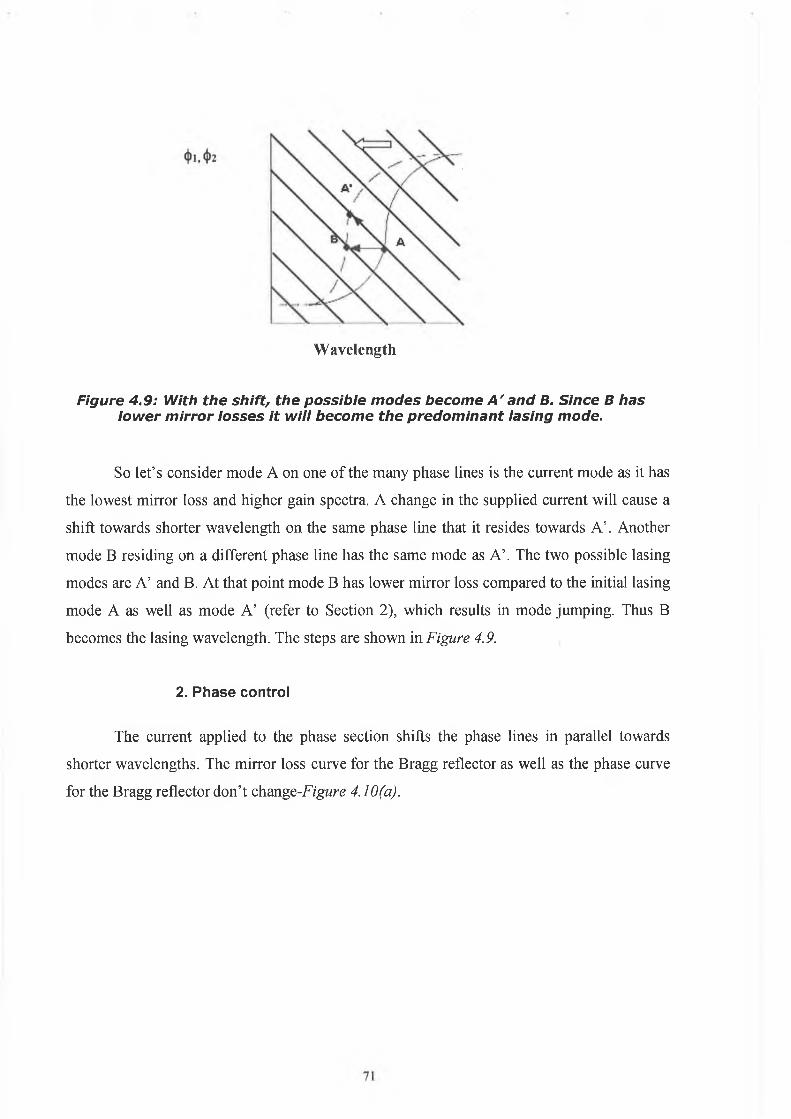
W avelength
Figure 4.9: With the shift, the possible modes become A ' and B. Since B has lower m irror losses it will become the predominant lasing mode.
So let’s consider mode A on one of the many phase lines is the current mode as it has
the lowest mirror loss and higher gain spectra. A change in the supplied current will cause a
shift towards shorter wavelength on the same phase line that it resides towards A ’. Another
mode B residing on a different phase line has the same mode as A ’. The two possible lasing
modes are A’ and B. At that point mode B has lower mirror loss compared to the initial lasing
mode A as well as mode A’ (refer to Section 2), which results in mode jumping. Thus B
becomes the lasing wavelength. The steps are shown in Figure 4.9.
2. Phase control
The current applied to the phase section shifts the phase lines in parallel towards
shorter wavelengths. The mirror loss curve for the Bragg reflector as well as the phase curve
for the Bragg reflector don’t change-Figure 4.10(a).

M irro r Loss
K \\ \ x \ ^<f>2
xX\
« //
/
♦i \A" ♦ *
v 7 \ \\ \
W avelength W avelength
Figure 4 .10: Change o f lasing wavelength under the influence of the phase control section. A) Phases versus wavelength B) M irror loss versus wavelength
With the increase o f the current the lasing modes moves in a cyclic manner A-A”-A’.
Therefore the induced change is limited to a certain value A. That is the reason why phase
tuning is used for fine adjustments o f the lasing wavelength only-see Figure 4.10(b) [12].
3. Simultaneous control of phase and front mirror section
Up till now an overview was made o f how the separate changes in the current o f the
different sections affect the operating wavelength. It will be outlined briefly what happens
when more than one sections are controlled simultaneously. The tuning mechanisms
previously described are applicable, the difference is that an analysis of two simultaneously
changing current should be made.
72

MirrorLoss
B'
s / \ /
1 ■ I
\%B" A"
Wavelength
Figure 4.11-Mirror Loss against wavelength
A wide range of wavelengths is accessible without any overlapping, whenever two
sections are controlled at the same time. This is achieved by changing the phase current
repeatedly and the Bragg current in a step like manner. The phase current is changed so point
A shifts to A ’ through A”. Then the Bragg current is changed till mode B coincides with A’.
By changing the phase again, mode B begins to lase and shifts to B ’ through B”-see Figure
4.11.
Iph
Wavelength
Figure 4 .12: Wide wavelength tuning by applying phase control current in arepeated fashion.
73

A. Quasi-continuous tuning
The quasi-continuous tuning involves simultaneous control of all the tuning sections as
described above. It provides complete wavelength coverage. The only factor that limits
tuning capabilities is the threshold increase and power decreases caused by bigger losses due
to the free carrier absorption and the heating with the injected current in the Bragg and phase
section [13].
B. Continuous tuning
The aim with continuous tuning is maintaining the longitudinal mode, while changing
in a certain way phase and front mirror sections simultaneously. The change in Bragg
wavelength should equal that of the phase section so the wavelength can be changed without
changing other wavelength conditions [14], Assuming that the refractive index change is
proportional to the square root of the injection current, the currents should satisfy the
following condition:
b [ b ^2
b Kb + Lb,(Equation 4.7)
IP, Ip-Currents of phase and front mirror section
La, Lb-Lengths of active and back mirror section
From the equation a suitable ratio for the currents can be derived. The advantage is
that with one current supply, two of the sections can be controlled. The perfect alignment of
the reflection peaks with the cavity mode corresponds to a minimum in threshold gain and
carrier density. As the active section voltage for fixed bias current depends on the carrier
density, it will also decrease.
Changing the currents for the mirror sections and the phase section induces shifts of
the comb mode spectrums and the longitudinal mode. Super mode jumps range between 4-
8nm (0.5-1.0 THz) and the longitudinal ones about 0.4nm(50GHz). The stable operating
points are defined away from the boundaries.
74

With varying the currents the output power and SMSR will change along with the
wavelength. When the wavelength is close to the Bragg region, the SMSR is maximum as the
Bragg’s section reflectivity is the highest for that region, so only a small fraction of light is
transmitted through the mirror section.
4.4 Complete characterisation of wavelength tuning of SG-DBR laser
In order to completely characterise an SG-DBR laser we have used the experimental
setup as shown in Figure 4.13. For initial characterization LabView is used. The PC and the
device are connected through general-purpose interface bus. The programme is set to change
the three currents, while recording the operating wavelength, the output power and SMSR.
Optical Spectrum
Figure 4.13-Set up for static characterisation of the SG-DBR laser
The programme is designed in such a way that currents are subsequently
changed by the means o f loops. The very first step is addressing all the devices-the
process is called initialisation during which the distant response is checked as well the
accessibility. Those devices include the spectrum analyzer, the temperature controller
o f the laser and current sources for the sections of the laser.
75

Figure 4 .14 - Flow chart. The building blocks o f the programme
All the currents, except the gain section current, which is fixed at 147 mA, then are
set to zero, which is the starting point o f the characterisation. The first loop sets the required
value for the current of the phase section. Immediately after setting value for it, the
programme leads to the second loop, where a new value for the front mirror section is
supplied. For those two fixed currents for the phase and front mirror section the third loop
provides a complete sweep through the whole range of values for the back mirror section in
steps o f 2mA. For each current value the wavelength, output power and side mode
suppression ratio is measured. After the limit is reached the third loop is exited. The
76

programme leads again into the second one and change the value for the front mirror section
after which the procedure with the third loop is repeated. Whenever the limit of the second
loop is reached the programme jumps to the first one changes the value of the current for the
phase section and goes again through the values of front and back mirror sections. This
characterisation is very time consuming as that means that measurements for hundreds of
particular values of the three currents have to be taken and summarised in a table. Figure 4.14
gives the flow o f the different steps following different exit points of the loops.
After the required data is gathered an application in Matlab is created so the
information can be visually displayed. All the information is divided in several phase planes.
Thus in a single phase plane the variables are limited to two: front and back mirror currents,
which can represent the X and Y axis of the plot, both of them representing a matrix z and the
investigated behaviour of the wavelength, power and SMSR can be subsequently plotted
using colour scale for the ranging values. A filled contour plot displays isolines calculated
from matrix z and fills the areas between the isolines using constant colours. The colour of
the filled areas depends on the current figure's colourmap. The functions that can be used are
contourf (x , y , z ) and contourf ( x , y , z , n) . They produce contour plots of z using x and
y to determine the x- and^-axis limits. X and Y are one-dimensional matrices that contain the
values of the front and back mirror currents respectively and Z is a two-dimensional matrice
that gives the value of the wavelength/output power or SMSR (depending on the purpose of
the plot).”n” gives the number o f different colours to be used in the plots. Those functions
have been used for the wavelength areas against the changes of the back and front mirror
currents. The plots should display the sampled grating mode hops as well as the longitudinal
ones. The heavy black lines are outlining the borders between the super mode jumps of 4-
8nm in wavelength and the light lines separate the regions o f longitudinal mode hops of 0.4
nm. Figure 4.15 depicts the wavelength borders between super mode jumps and longitudinal
jumps.
Let’s consider a scenario where the laser needs to be tuned from point A to B,
corresponding to particular accessible wavelength modes. While sweeping through the
currents of the front and back mirror sections the wavelength would experience several
changes.
77

Figure 4 .15-P lot o f mode and longitudinal hopping against the front and backm irror currents
The first o f them would be a longitudinal mode jump, followed by super mode jump,
when it crosses the heavy black line to enter another wavelength region and the last transition
is another two jumps caused by longitudinal mode hopping. The succession of the transition
can be followed on the Figure 4.16.
FrequencyIIHtJ
Current
Figure 4 .1 6 - Frequency change with simultaneous control o f front andback m irror section
78

As discussed above on the plot the different isolines form areas with different colour.
The plot should be interpreted in the following manner: The tunable wavelength region from
1525 to 1575nm can be divided in several smaller ones comprising a small range of
wavelengths. The boundaries o f the super mode jumps produce a fan. The different regions
from the fan stand for different wavelength changes between two consequent super mode
jumps. Depending on the tuning currents of the back and front mirror sections different
ranges are accessible. In the current limits of those two sections some of the ranges are
repeated-see Figure 4.17. For best performance the actual applied current should be the
lowest possible to achieve the required wavelength. This rule is important as one wavelength
can be obtained by applying different combination of currents. Out of those combinations the
lowest possible should be selected, as this would remove the problem with heating of the
section and increasing the settling time. As the phase section control provides for fine-tuning,
results are taken for several different phase planes. Interpolation between them provides look
up table currents.
Figure 4.17-Contour map o f the tuning wavelength regions for different frontand back m irror currents
The longitudinal modes should be marked as well: regions within different super
mode jumps have different green colour, opposed to longitudinal cavity jumps, which have
79

different transverse shades of green. Figure 4.18 represents an extraction from the above
contour map. If the work wavelength region is within one of the presented super mode jumps,
the change o f the phase current shifts the wavelength slightly, providing fine-tuning of
0.4nm. That is the reason it is essential that the measurements are performed in more phase
planes so at the wavelengths and the corresponding tuning currents are defined with high
precision. If the channels are too close spaced relatively to each other the effect of the
interference cannot be neglected.
a«uUSUs-ouLm
Front Mirror Current
Figure 4.18-Contour map for different front and back m irror currents outliningthe longitudinal modes
For achieving stable operation points the output power in addition to the emission
wavelength, must be monitored. One and the same wavelength can be accessed through a
various combinations o f back and front mirror currents. The best way of deciding upon which
pair of currents is to be selected for the particular wavelength is monitoring the output power.
In Figure 4.19 two plots for the output power are provided. One o f them is for 5mA supplied
phase current, the other for 20mA. Comparing the two plots it can be seen that there are more
points in the lower current plane with high power. Partially the explanation for this is that
with higher value of the currents the output power deteriorates because of the heating of the
80

sections which causes changes in the bandgap structure o f the laser-such as bandgap
shrinkage. For an optimal decision different points need to be taken into account in various
phase planes, that is why the current for the phase section has been changed in steps of two
along with the two other sections.
0 Back Mirror Current 96
Figure 4 .1 9 - Output pow er for different back and front m irror mirrors in twodifferent phase planes
If a particular region is taken under inspection and the colour coding is changed a
better idea can be obtained for the variation of the power with the slightest changes in the
81

applied currents. The output power is not related to the achieved wavelength but rather to the
extent o f alignment of the mirrors. The output power, which is measured with respect to the
front and back mirror currents experience saddle points: a minimum with respect to the front
mirror coincides with a maximum with respect to the back mmox-Figure 4.20.
In the absence of carrier induced absorption losses in the reflector, a saddle point
would occur at the point where a peak of each reflector is exactly aligned with the same
cavity mode. On Figure 4.20 the saddle points appear as white spots that are standing for
maximum output power.
The increase o f the losses with the current causes the saddle point to shift towards
lower rear and higher front DBR currents. For very high currents the saddle point can even
disappear. The effect is largest for the front mirror as the output light passes through it twice.
Back Mirror Current
Figure 4.20-Colour grid for the output power
So far it has been shown that controlling the four section simultaneously for tuning to
a particular wavelength is not an easy task. The wavelength accessibility is very important in
addition to the precision of the tuning in order that interference be avoided. Any drift in the
operating wavelength can cause interference between the channels. Many of the commercial
tunable lasers have built in circuits for wavelength monitoring as well as control circuits for
stabilizing the operating wavelength and protecting against drifts caused by overheating of
the laser sections. In the following section some o f these schemes will be reviewed.
82

4.5 Stabilization scheme
When an SG-DBR laser is deployed in a network, a control o f the different
parameters must be exerted, as well as a way of monitoring its behavior. Creating a look up
table is an essential part of the process, as the most likely scheme of controlling the laser will
be using a microprocessor to drive the current sources to the different sections. The data
containing the appropriate values for the currents will be stored in a memory. The processor
will read those values and the right currents will be injected.
Feedback control loops are required for achieving stable operating points. The
channel currents must be adjusted based on the principle that the operating point should not
reside near the mode boundaries. It is necessary not to jeopardize the modal stability, while
maintaining the output frequency.
For that reason two different control loops are required. As the concept for the
feedback control schemes are outside the scope of thesis work only a short outline of the each
methods will be provided.
1.Frequency stabilization
High precision o f the tuning can be achieved by changing the current of the phase
section while the output wavelength is monitored using a wavelength meter or optical
spectrum analyzer. The output from the meter may be used as external reference and
according to their reading the current is appropriately adjusted [16],
2.Mode stabilization
By deploying only the frequency feedback loop there is no guarantee that high SMSR
is maintained. A correlation between SMSR and variation of the output power has been
reported. A high SMSR can be obtained by locking to a saddle point in the output power. The
drawbacks of this approach are that other parameters like reflector losses with increased
current are not taken into account and alignment between the longitudinal and reflector
modes cannot be assured. Monitoring the active section voltage proves to be a solution [17].
The idea is that the voltage depends on the carrier density.
83

(Equation 4.8)
N-carrier concentration r\-carrier confinement factor I(t)-current kp-Boltzman constant q-electorn chargeNo, Ny-donor and acceptor concentrations of the N-type and P-type materials that
make the junction of the active section
The voltage as it can be seen is assumed to follow the carrier concentration. The
carrier density and the threshold gain have their minimums only for perfect alignment o f the
reflectivity peaks, thus providing for minimum voltage for the active section.
Monitoring the voltage and locking subsequently to the lowest level secures high
SMSR and perfect alignment o f the mirrors peaks.
4.6 Other parameters
The most important feature of tunable transmitters such as the tuning range and
number of accessible channels was fully analyzed and explained earlier. For complete
understanding o f the Sampled Grating DBR lasers and their characterization some o f the
other important parameters have to be mentioned as well.
4.6.1 Spectral linewidth
Narrow spectral linewidth is fundamental for DWDM systems. The following
expression gives the parameters that have influence on the overall spectral linewidth of the
laser:
s n p(Equation 4.9)
7jsp -spontaneous emissionh-Plank’s constant v-optical frequency
84

P-light output g-gaina m -mirror loss v -group velocity
a-linewidth enhancement factor, where a=(dn/dN)(dG/dN)N-carrier density n-refractive index
The linewidth o f the SG-DBR laser is not constant: it varies widely. Values typically
range between 3-10 MHz. There is a reported dependence on the tuning of the back, front
mirror and phase section currents [18]. The largest broadening occurs with increasing the
current o f the phase section.
It is found that the linewidth is proportional to the square of the mode spacing. Thus a narrow
linewidth requires a long cavity with small mode spacing, whereas a short cavity gives good
SMSR. In a case o f long cavity there are several modes within the main lobe of the Bragg
reflector and the SMSR is rather poor. The oscillation in two or even more modes is likely to
occur close to a mode jump causing large linewidth.
The relative intensity noise serves as a measuring tool of the noise characteristics o f
emitted optical power from the laser. The intensity fluctuations are usually characterized by
RIN measurements. The relative intensity noise measurements are performed by analysing
the electrical spectrum of the laser light at a fixed bias current converted by a high-speed
photodiode. As the thermal and the shot noise in the photodetector contribute to the noise of
the system for identifying the RIN of the laser, those terms should be subtracted.
RINsys=RINiaser+RINthermai+RINshot (Equation 4.10)
4.6.2 R IN
fibre
RINlaser = RIN„ N thermal 2qIdcRcP T1 /?
el,ave eie L
H(w)-modulation transfer function w-electircal frequency
85

WR-relaxation resonance frequency h-Plank’ constant v-optical frequency Po-optical power r|-photodiode response Pfibre-power coupled into fibre
Figure 4.21 shows the contribution of the different factors on the overall RIN
-110
RIN
[dBVHz]
Total RIN
of the system
Shot noise-1/P- V - »
\V
Laser RIN
■ 160 -v.\
Optical power (mW)
Figure 4 .21 -R IN versus frequency a t different bias currents.
Figure 4.22 displays the RIN performance of the whole system for different active section
currents.
Frequency (GHz)
Figure 4 .22 - R IN versus fibre coupled power with active section biased
86
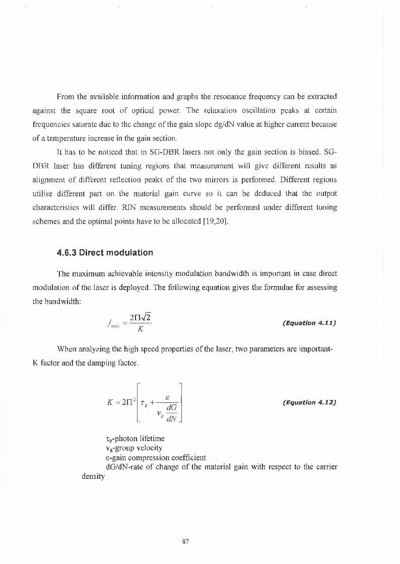
From the available information and graphs the resonance frequency can be extracted
against the square root o f optical power. The relaxation oscillation peaks at certain
frequencies saturate due to the change o f the gain slope dg/dN value at higher current because
of a temperature increase in the gain section.
It has to be noticed that in SG-DBR lasers not only the gain section is biased. SG-
DBR laser has different tuning regions that measurement will give different results as
alignment o f different reflection peaks o f the two mirrors is performed. Different regions
utilise different part on the material gain curve so it can be deduced that the output
characteristics will differ. RIN measurements should be performed under different tuning
schemes and the optimal points have to be allocated [19,20],
4.6.3 Direct modulation
The maximum achievable intensity modulation bandwidth is important in case direct
modulation o f the laser is deployed. The following equation gives the formulae for assessing
the bandwidth:
2 lW 2/max = ...— ( Equat i on 4.11)
When analyzing the high speed properties of the laser, two parameters are important-
K factor and the damping factor.
K = 21T r ,+ - dGdN
(Equation 4.12)
density
Tp-photon lifetimeVg-group velocityE-gain compression coefficientdG/dN-rate o f change of the material gain with respect to the carrier
87

The intrinsic limits of the device performance can be determined by the damping
factor as well. Theoretically the damping factor is proportional to the square of the resonance
frequency. In fact it is calculated by the following formulae:
y = K fl + y0 (Equation 4.13)
For large resonance frequencies, the K factor describes the damping of the response,
the damping factor offset yo is important at low laser power when the relaxation oscillation
frequency is small. So it can be summed up that K-factor is used to estimate the maximum
intrinsic bandwidth (damping limited) in the absence o f other limitations.
After having the two parameters the ultimate damping 3dB limited bandwidth can be
calculated [21],
Most semiconductor lasers solve the light confinement problem by introducing a
change in the refractive index in lateral direction. In strongly index guided lasers, the active
region is buried on all sides by several layers of lower refractive index materials as the laser
we were using. This structure is called buried heterostructure. A p-n-p-n thyristor blocking
structure is often used to confine the current but it contributes to parasitic capacitance, which
reduces the modulation performance of the laser.
4.7 Conclusions
Theoretical model for four-section SG-DBR laser static tuning was presented as well
as a complete experimental characterisation of SG-DBR laser was undertaken to determine
the tuning characteristics. The tuning properties were studied in terms of currents, linewidth,
SMSR and output power. Regions of continuous tuning for the laser were presented and
different limitations on the continuous tuning range were clarified. The last chapter will deal
with the dynamic tuning of these types of lasers and the effect on the overall performance of
the network provided more than one tunable module is functioning.

References:
1. J. Stohs, D. J. Bossert, D. J. Gallant, S. R. J.Brueck, ’Gain, refractive index change, and
linewidth enhancement factor in broad-area GaAs and InGaAs quantum-well lasers’, IEEE
Journal o f Quantum Electronics, Volume: 37, Issue: 11, pp: 1449 - 1459, Nov. 2001
2. B. R. Bennett, R. A. Soref, J. A. Del Alamo, ’Carrier-induced change in refractive index
of InP, GaAs and InGaAsP’, IEEE Journal of Quantum Electronics, Volume: 26, Issue:
1, pp:l 13 - 122, Jan. 1990
3. D. Green, ‘Semiconductor Lasers’, 2003
4. P. Kozodoy, T. Strand, Y. Akulova (Agility Communication); Z. Bian, J. Christofferson
(University of California), ‘Thermal Effects in Monolithically Integrated Tunable Laser
Transmitters’, Twentieth Annual IEEE Semiconductor Thermal Measurement and
Management Symposium, 2004., pp:177 - 1839, 11 Mar 2004
5. P. A. Morton, V. Mizrahi, T. Tanbun-Ek, R. A. Logan, P. J. Lemaire, ‘Stable Single Mode
Hybrid Laser with high Power and Narrow linewidth’, Applied Physics Letters, Volume 64,
Issue 20, pp.2634-2636, May 16, 1994,
6. I. A. Avrutsky, M. Fay, J. M. Xu, ‘Multiwavelegth Diffraction and Apodization Using
Binary Superimposed Gratings’, IEEE Photonics Technology Letters, Vol. 10, No. 6, pp:839
-8 4 1 , June 1998,
7. J. Skaar, O. H. Waagaard, ’Design and characterization of finite-length fiber gratings’,
IEEE Journal of Quantum Electronics, Volume: 39, Issue: 10, pp: 1238 - 1245, Oct. 2003
8. G. Wimpenny, M. J. Adams, ‘Comparison of Grating Analysis Techniques for SG-DBR
Lasers’, Microwave and Optical Technology Letters, Vol.40, No.2, pp: 161-164, 20 January
2004
9. G. Starlet, G. Morthier, R. Baets, ‘Wavelength and Mode Stabilization of Widely Tunable
SG-DBR and SSG-DBR Lasers’, IEEE Photonics Technology Letters, Vol.11, N o.11,
November 1999, Pages: 1351 - 1353
10. R. J. Simes, Y. A. Akulova, C. W. Coldren, M. C. Larson, ‘Inp Chip Scale Integration
Platform for High Performance Tunable Lasers’, Spie Proceedings, 2003
11. H. -F. Liu; S. Arahira, T. Kunii, Y. Ogawa, ’Tuning characteristics of monolithic
passively mode-locked distributed Bragg reflector semiconductor lasers’ ,IEEE Journal of
Quantum Electronics, Volume: 32, Issue: 11,, pp:1965 - 1975, Nov. 1996,
89

12. K. Kobayashi, I. Mito,’Single frequency and tunable laser diodes’, Journal of Lightwave
Technology, Volume: 6, Issue: 11, pp: 1623 - 1633, Nov. 1988
13.B. Mason, G. A. Fish, S, P. DenBaars, L. A. Coldren, ‘Sampled grating DBR lasers with
22 nm quasi-continuous tuning and monolithically integrated wavelength monitors’,
Semiconductor Laser Conference, 1998. ISLC 1998 NARA, 1998 IEEE 16th International
, pp:267 - 268, 4-8 Oct. 1998,
14. H. Ishii, H. Tanobe, F. Kano, Y. Tohmori, Y. Kondo, Y. Yoshikuni, ’Quasicontinuous
wavelength tuning in super-structure-grating (SSG) DBR lasers’,
IEEE Journal of Quantum Electronics, Volume: 32, Issue: 3, pp:433 - 441, March 1996
15. O. Ishida, Y. Tada, H. Ishii, ’Tuning-current splitting network for three-section DBR
lasers’, Electronics Letters, Volume: 30 , Issue: 3 , pp:241 - 242, 3 Feb. 1994,
16. F. Kano, Y. Yoshikuni, H. Ishii, ‘Frequency control and stabilization of broadly tunable
SSG-DBR lasers’, Optical Fiber Communication Conference and Exhibit, 2002. OFC
2002, pp: 538 - 540, 17-22 March 2002
17. G. Sarlet, G. Morthier, R. Baets, ’Control o f widely tunable SSG-DBR lasers for dense
wavelength division multiplexing’, Journal of Lightwave Technology, Volume: 18, Issue:
8, pp: 1128- 1138, Aug. 2000
18. H. Ishii, F. Kano, Y. Tohmori, Y. Kondo, T. Tamamura, Y. Yoshikuni, ’Narrow spectral
linewidth under wavelength tuning in thermally tunable super-structure-grating (SSG) DBR
lasers’, IEEE Journal of Selected Topics in Quantum Electronics, Volume: 1 , Issue: 2 , pp:
401 -407June 1995
19. Y. A. Akulova, G. A. Fish, P. -C. Koh; C. L. Schow, P. Kozodoy, A. P. Dahl, S.
Nakagawa, M. C. Larson, M. P. Mack, T. A. Strand, C. W. Coldren, E. Hegblom, S. K.
Penniman, T. Wipiejewski, L. A. Coldren, ’Widely tunable electroabsorption-modulated
sampled-grating DBR laser transmitter’, IEEE Journal of Selected Topics in Quantum
Electronics,, Volume: 8 , Issue: 6 , pp: 1349 - 1357, Nov.-Dec.2002
20. S. Nakagawa, G. Fish, A. Dahl, P. Koh, C: Schow, M. Mack, L. Wang, R. Yu, ’Phase
noise of widely-tunable SG-DBR laser’, Optical Fiber Communications Conference, 2003.
OFC 2003 , pp: 461 - 462 vol.2, 23-28 March 2003
21. M. L. Majewski, J. Barton, L. A. Coldren, Y. Akulova, M. C. Larson, ’Direct intensity
modulation in sampled grating dbr laser’, IEEE Photonics Technology Letters, Volume:
14, Issue: 6, pp:747 - 749, June 2002
90

Chapter 5
BER Performance in Wavelength Packet Switched WDM Systems During Nano-second Wavelength Switching Events
5.1 Introduction
In a complete WDM system that employs wavelength packet switching, each
transmitter can tune its emission wavelength to transmit packets of information at a
number of different wavelengths. The information from all the transmitters can then
be multiplexed together and sent over optical fibre. The composite wavelength signal
may then pass through an Array Waveguide Grating (AWG), which sends each of the
incoming wavelengths to one specific output fibre port. In general it is possible to
write the wavelength connectivity in form of a matrix. Thus by choosing an
appropriate wavelength on the transmitter side, the laser selects the output port to
which the information packet is sent. The tuneable transmitters, together with the
optical coupler and the AWG, become a strictly non-blocking switch fabric with a
switching speed equal to the tuning speed of the laser [1,2],
Clearly the key component for implementing such networks is the wavelength
tuneable laser transmitter, as the overall design of the wavelength packet-switched
WDM networks will be heavily dependent on the characteristics of these tuneable
devices. The main characteristics that determine the usefulness of wavelength
tuneable lasers in wavelength packet-switched systems are the wavelength tuning
range, the side-mode suppression ratio (SMSR), the output power, and the speed at
which the device can switch from one wavelength to another. Taking into account
these characteristics, the most suitable tuneable lasers for use in wavelength packet-
switched systems are electronically tuneable devices [3], Typical examples of such
devices are grating-assisted co-directional coupler with sampling grating reflector
(GCSR) lasers [4,5], and super structure grating distributed Bragg reflector (SSG-
DBR) lasers [6-9], These devices can achieve tuning ranges in excess of 60 nm,
SMSR’s exceeding 30 dB, output powers above 10 dBm, and switching times in the
order or 20-50 ns. Another important feature of these electronically tuneable lasers is
91
that as the transmitter is being switched between a low and a high wavelength
channel, it is possible that the device will emit intermediate wavelengths during the
switching event. This effect may clearly cause serious problems in an overall
wavelength packet-switched WDM network as the optical output from the tuneable
laser, as it transitions between two specific wavelengths, may result in cross-channel
interference on other wavelength channels in the WDM network. This may ultimately
limit the Bit-Error-Rate (BER) performance of specific data channels in the network.
The work carried out in this chapter was undertaken using a nano-second
wavelength switched laser module that uses DBR technology. The switching time of
this module was initially being characterized by encoding a data packet onto the
tuneable laser output, such that the data spans the transition period between two output
wavelengths, and then examining the eye diagram of the resulting signal at both output
wavelengths. From the experiment the switching time was determined. The output from
the tuneable laser (TL) module was then multiplexed with a second laser transmitter
(that is generating data at a wavelength channel that lies between the 2 wavelengths
that the TL is switching between). From this work the degradation in system
performance on the central data channel, due to the spurious wavelength signals
emitted from the TL during the switching event, is confirmed by the presence of an
error floor in the BER vs. received power measurements. Certain levels of attenuation
are required at the output of the TL module such that BER’s of 10'9 or better can be
obtained for the data channel that lies between the two wavelengths that the TL module
is switching between.
5.2 Switching time
Fast wavelength switching in the nanosecond regime combined with a
wavelength selective device enables the routing of data packets. A critical requirement
for an efficient optical fabric is that switching time between any channel combinations
of the transmitter has to be short compared with the data packet length. The actual
switching time depends on three parameters, namely:
92

1. Structure of the laser-the current settling times are highly dependant
primarily on the laser chip capacitance and the dynamic resistance of the tuning
section. Investigating carrier dynamics is a very complicated process, but it should be
noted that for the most common deployed structures for those particular laser-buried
heterostructure- there is so called p-n-p-n thyristor current blocking structure for
current confinement, which yields high internal parasitic capacitance and thus hinders
the switching performance [10],
2. C arrier lifetime-the typical carrier lifetime in semiconductor lasers,
owing to the spontaneous emission is of order of several nanoseconds at threshold. The
rate of spontaneous emission is very dependant on the carrier density [11]. It can be
deduced that the switching will be greatly influenced be the injected current and
different processes of recombination depending on the actual structure of the laser.
3. Driver electronics-even though the concept is simple: the current should
be injected in the passive section in a square wave manner such that different levels
correspond to certain injected electron density, which leads to carrier change and
refractive index change, different parameters present an obstacle. Different approaches
for developing high-speed circuits for fast wavelength switching can be adopted. One
way is deploying a field programmable gate array with embedded microprocessor and a
look up table. Every time a targeted channel is given the required currents are checked in
the table and the tuning current are then processed by digital to analog converters,
amplified to the required level and sent to the tuning sections [12], Another approach is
using an IC driver, mounted on an alumina substrate. To achieve fast switching times the
driver uses GaAs depletion pseudomorphic high electron mobility transistor (P-HEMT)
[13]. A relatively new approach is the optical printed circuit board-a platform towards
VLSI Nano Photonics. The O-PCB is very much like that of electrical printed circuit
board except that the former uses optical wires for optical signals [14],
CMOS 1C laser drivers are potential choices for developing high-speed board
[15]. The current going into the mirror section of the laser can be easily programmed,
which respectively gives the option by changing the value to access different channels.
Several issues should be dealt separately.
93

• Small changes in the bias voltage result in large changes in the supplied current,
which accordingly causes switching of channels. Because of the required fast
change in the current inductive voltage spikes are produced therefore the
modulation current should be AC coupled [16],
• Damping resistor-connected in series with the laser section, which usually has
resistance between 3-5 ohms (it varies with the current supplied), raises the load
resistance, thus reduces the load frequency dependence [17]
• Taking into consideration that laser package series inductance cannot be
eliminated completely, a compensation network should be designed in order to
reduce it. The parasitic inductance and capacitance of the interconnect paths
between packaged devices will cause severe ringing problems. No low loss
impedance matching is possible for the laser interconnection as the laser
impedance drops low with increasing drive current. That means the current must
be fed into a variable and low dynamic impedance load. The load of the laser can
be considered to be 4 ohms and 4nH,adding a damping resistor and a coupling
capacitor, a R/C compensation network is recommended. It should be placed as
close to the load as possible. Since the provided offset for the modulating current
is attached directly, issues with he parasitic capacitance should be dealt with as
well. Solution to the problem is adding R/L network in series [18],
Perfect impedance matching is very hard to be achieved. All the networks placed
to compensate for different parasitic issues can operate properly only in a certain
frequency region. Due to the parasitics and the not so sharp transition edges of the current
steps different intermediary wavelength modes are aroused as it is shown on Figure 5.1.
94
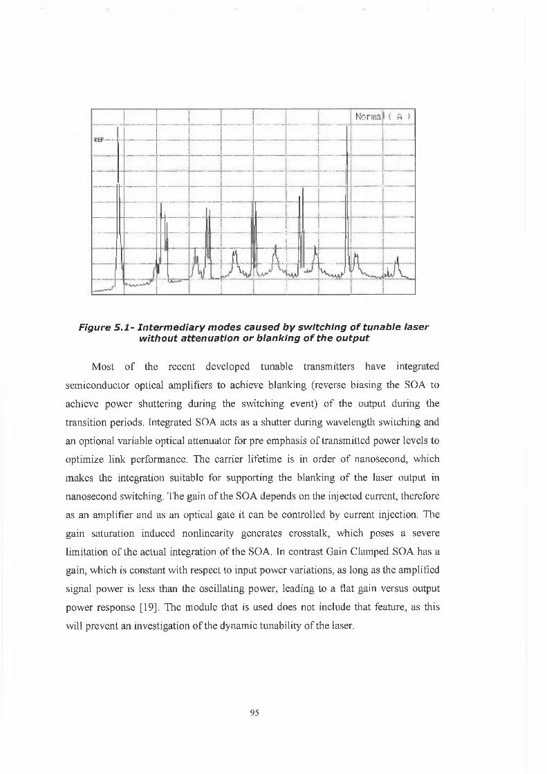
Figure 5 .1 - Interm ediary modes caused by switching of tunable laser without attenuation or blanking of the output
Most of the recent developed tunable transmitters have integrated
semiconductor optical amplifiers to achieve blanking (reverse biasing the SOA to
achieve power shuttering during the switching event) of the output during the
transition periods. Integrated SOA acts as a shutter during wavelength switching and
an optional variable optical attenuator for pre emphasis of transmitted power levels to
optimize link performance. The carrier lifetime is in order of nanosecond, which
makes the integration suitable for supporting the blanking of the laser output in
nanosecond switching. The gain of the SOA depends on the injected current, therefore
as an amplifier and as an optical gate it can be controlled by current injection. The
gain saturation induced nonlinearity generates crosstalk, which poses a severe
limitation of the actual integration of the SOA. In contrast Gain Clamped SOA has a
gain, which is constant with respect to input power variations, as long as the amplified
signal power is less than the oscillating power, leading to a flat gain versus output
power response [19]. The module that is used does not include that feature, as this
will prevent an investigation of the dynamic tunability of the laser.
95

5.3 Determination of tunable laser switching time
To determine the switching time of the TL module we have employed the
experimental test-bed as presented in Figure 5.2.
Figure 5.2-Experimental configuration to determine switching time of TLmodule
The module is controlled via a PC and can be set to transition between different
wavelengths on the ITU grid. A trigger output from the wavelength tunable module is
available to determine the timing of the transition between wavelengths from the TL.
This trigger signal is then fed into a signal generator that can produce variable width
pulses at the same repetition rate that the laser transitions from one wavelength to
another. The output from this signal generator is subsequently fed into the Pattern
Generator such that bursts of data, at a rate of 2.5 Gbit/s, can be applied to one
specific wavelength channel, and the length of the burst and position of the burst
relative to the laser transition time, can be varied using the signal generator.
The information is encoded onto the optical output from the TL using an
external modulator with a bandwidth 8 GHz. A polarization controller (PC) is required
before the modulator to ensure that the signal entering the PC has the correct
polarization. The data signal from the pattern generator is fed directly into the RF port
96
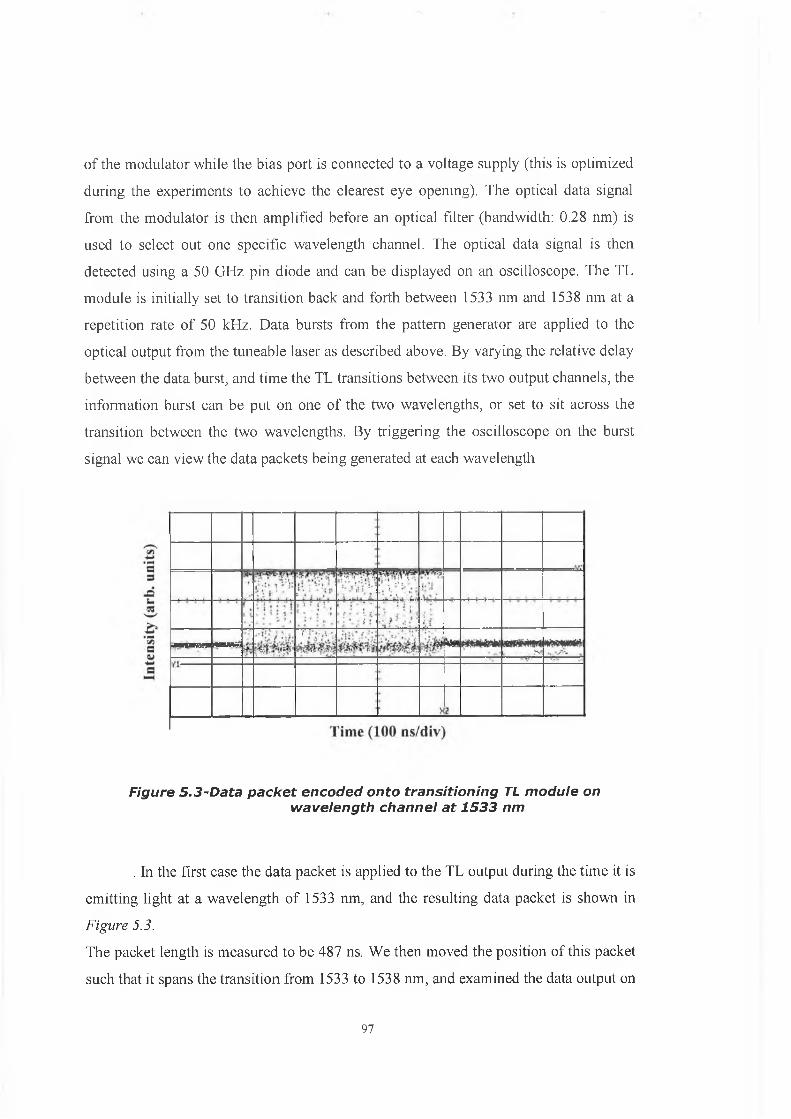
of the modulator while the bias port is connected to a voltage supply (this is optimized
during the experiments to achieve the clearest eye opening). The optical data signal
from the modulator is then amplified before an optical filter (bandwidth: 0.28 nm) is
used to select out one specific wavelength channel. The optical data signal is then
detected using a 50 GHz pin diode and can be displayed on an oscilloscope. The TL
module is initially set to transition back and forth between 1533 nm and 1538 nm at a
repetition rate of 50 kHz. Data bursts from the pattern generator are applied to the
optical output from the tuneable laser as described above. By varying the relative delay
between the data burst, and time the TL transitions between its two output channels, the
information burst can be put on one of the two wavelengths, or set to sit across the
transition between the two wavelengths. By triggering the oscilloscope on the burst
signal we can view the data packets being generated at each wavelength
Figure 5.3-Data packet encoded onto transitioning TL module onwavelength channel at 1533 nm
. In the first case the data packet is applied to the TL output during the time it is
emitting light at a wavelength of 1533 nm, and the resulting data packet is shown in
Figure 5.3.
The packet length is measured to be 487 ns. We then moved the position of this packet
such that it spans the transition from 1533 to 1538 nm, and examined the data output on
97

both of the wavelength channels by tuning the optical filter between the two
wavelengths. For the output at 1533 nm the initial bits of the data packet are clean, but
as we approach the transition, and the output wavelength moves away from 1533 nm,
the eye starts to close (as shown in Figure 5.4).
Clean eye back to start of Eye closing as laser begins to transitions from 1533data burst (248 ns) to 1538 nm. Pattern disappears 20 ns from this point
Time (1 ns/div)Figure 5.4-Portion o f received data packet at 1533 nm with data encoded
onto TL module such that it spans transition from 1533 to1538 nm
The time interval for which the eye diagram is completely open and the TL can
be used for error-free transmission at this wavelength is measured to be 248 ns. We
then tuned the filter to select the output at 1538 nm, in this case the final bits of the data
packet are clean, but the initial bits have closed eyes due to the fact the laser is in the
process of transitioning to 1538 nm from 1533 nm {Figure 5.5).
98

Time (500 Ds/div')Figure 5.5-Portion o f received data packet at 1538 nm with data encoded
onto TL module such that it spans transition from 1533 to1538 nm
The time interval for which the bits are clean and the TL can be used for error-
free transmission at this wavelength is 202 ns. By adding up the time intervals for
which the TL module can be used for error-free transmission at the two wavelengths it
is transitioning between, we obtain a total of 449 ns. As the total length of the data bust
is 487 ns, we can determine that the transition time (switching time) during which we
are unable to transmit data error-free on either of the output wavelengths is 38 ns.
5.4 Effects of TL output during switching event
To investigate how the BER transmission performance of a WDM channel is
affected by the output from the TL module that is transitioning between two
wavelengths on either side of the data channel being monitored, we have used the
experimental set-up shown in Figure 5,6.
In this case the TL module is once again set to transition back and forth between 1533
and 1538 nm at a repetition rate of 50 kHz. In addition to the TL we use a HP
wavelength tunable external cavity laser (ECL) that can emit light from 1480 to
1570nm. 2.5 Gbit/s electrical data signal (2U-1 PRBS) from the pattern generator is
Eye closing as laser transitions to 1538 from 1538 nm. Pattern disappears 20 ns back from this point
Clean eye to the end of data burst
99
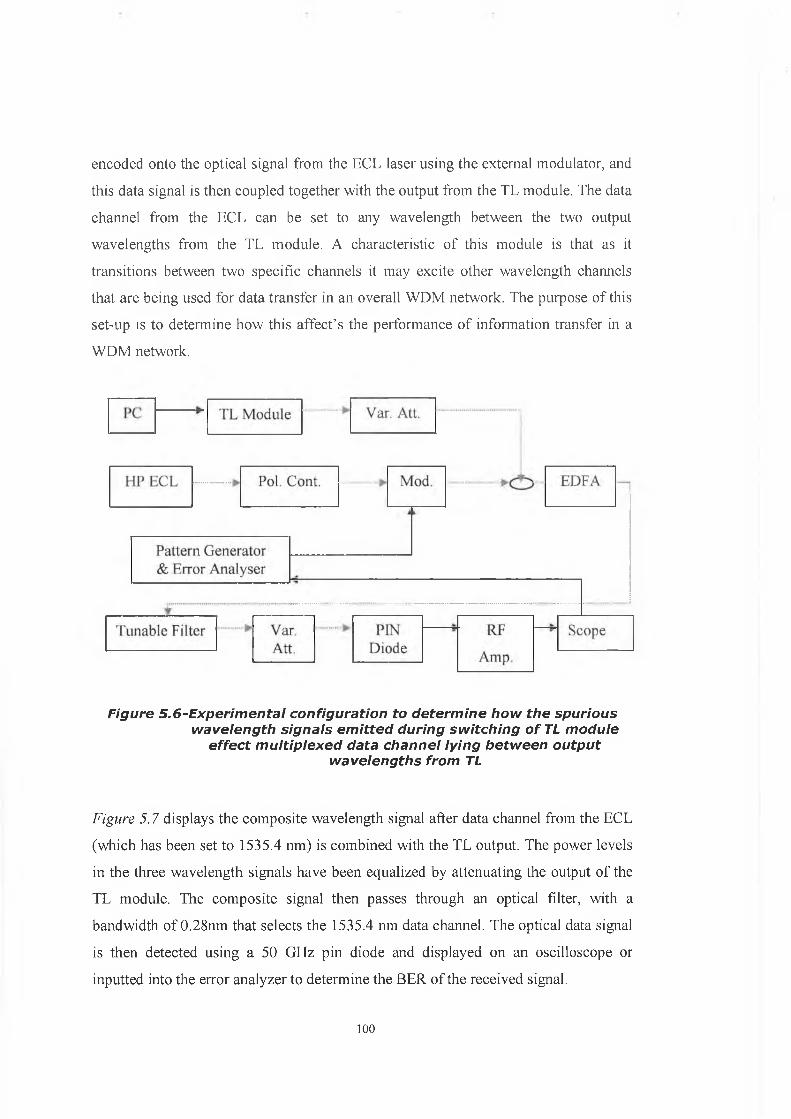
encoded onto the optical signal from the ECL laser using the external modulator, and
this data signal is then coupled together with the output from the TL module. The data
channel from the ECL can be set to any wavelength between the two output
wavelengths from the TL module. A characteristic of this module is that as it
transitions between two specific channels it may excite other wavelength channels
that are being used for data transfer in an overall WDM network. The purpose of this
set-up is to determine how this affect’s the performance of information transfer in a
WDM network.
Figure 5.6-Experimental configuration to determine how the spurious wavelength signals emitted during switching of TL module
effect multiplexed data channel lying between output wavelengths from TL
Figure 5.7 displays the composite wavelength signal after data channel from the ECL
(which has been set to 1535.4 nm) is combined with the TL output. The power levels
in the three wavelength signals have been equalized by attenuating the output of the
TL module. The composite signal then passes through an optical filter, with a
bandwidth of 0.28nm that selects the 1535.4 nm data channel. The optical data signal
is then detected using a 50 GHz pin diode and displayed on an oscilloscope or
inputted into the error analyzer to determine the BER of the received signal.
100

Figure 5.7-Composite wavelength signal after coupling together output from TL module (switching back and forth between 1533 and
1538 nm) and data channel from ECL a t 1535.5 nm
To determine whether the signals excited by the tunable module (as it
transitions between two wavelengths on either side of the data channel) affect the
system performance, we must first of all plot the back to back performance of the
1535.4 nm data channel on it’s own. The BER vs. received power for the back-to-
back case is shown in Figure 5.8.
It should be noted that the low receiver sensitivities in this figure are as a result
of the low receiver gain used in the present experiment. We then proceed to measure
the BER vs. received power for the case when the data channel is coupled together with
the TL module output before being filtered out (also shown in Fig. 7, 0 dB attenuation
curve). In this case the power levels in the three wavelength signals have been
equalized. The associated eye diagrams of the received data signals for the single
channel case, and the case when the data channel is multiplexed with the tunable laser
(that is switching between two wavelengths), before being filtered out and detected, are
shown in Figure 5.9.
101

R e c e i v e d p o w e r [ d B m ]
Figure S.8-BER vs. received power for back-to-back case, and for case when the data channel is multiplexed with output from the TL
Module (as a function o f attenuation of the TL output)
From these eye diagrams we can clearly see the noise added to the data signal
as a result of the TL laser generating a spurious wavelength output at the same
wavelength as the monitored data channel, during its transition between two output
wavelengths. The effect of this on the BER vs. received power curve is to place an
error floor on the performance of the monitored data channel. The error floor is at 4 x
10° (as shown in Figure 5.7), and is a result of the TL generating light at intermediary
wavelengths (including 1535.4 nm) for a small period of time during the transition
from 1533 to 1538 nm. Similar error floors were obtained when the data channel was
set to wavelengths corresponding to the other spurious wavelengths that are generated
during the transition period of the TL module. Figure 5.10 displays the BER vs.
received power curves for the case when the ECL is tuned to three different wavelength
102

channels (1534.2, 1535.4, and 1536.6 nm) between the output wavelengths being
emitted from the TL.
(a)
Time, 100 ps/div
Figure 5.9-Received eye diagrams for the 1535.5 nm channel for (a ) the back-to-back case, and (b ) for the case when the data
channel is multiplexed with the tunable laser output before being filtered out and detected
103

1.00E-01
1.00E-02
-13 -12 -11 -10 -9 -8 -7 -6
Received power [dBm]
Figure 5.10-BER vs. received power when the data channel from ECL is tuned to three different wavelengths between output wavelengths from TL module (triangles : 1534.2 nm ; squares : 1535.4 nm ; circles : 1536.6 nm)
From the measured error-floor it is possible to estimate the length of time that
the TL output is at the same wavelength as the monitored data channel, during its
transition. This can be achieved in the following manner: the TL is transitioning
between its two output wavelengths every 10 microseconds, and since we are sending
information at 2.5 Gbit/s, in 10 microseconds we send approx. 25000 bits. With a BER
of 4 x 10°, this means that 1 of the 25000 bits sent in 10 microseconds is received in
error due to the excitation of the intermediary wavelength channel. However given that
the signal generation from the tunable laser only gives an error for a sent “0”, and given
that we send unbiased data (equal number of “ l ’s” and “0’s”), we can assume that the
intermediary wavelength is on for approx. 2 bit periods of the 2.5 Gbit/s data signal, or
800 ps.
The limitation on BER performance on the monitored data channel that we have
investigated in this work (due to the spurious wavelength output from the TL module
during it’s transition period) is clearly a major issue for the development of large-scale
WDM networks employing tunable lasers for wavelength packet-switched
104

architectures. In order to overcome these limitations in real WDM communication
systems using wavelength packet switching, it will be vital to extinguish the output
from the TL as it transitions between specific wavelength channels. This will ensure
that the spurious wavelengths emitted from the tunable laser as it transitions, do not
limit system performance. To determine the required level of signal extinction at the
TL module output, such that it will not affect system performance in a wavelength
packet-switched WDM system, we have used the experimental arrangement described
earlier. In this work we have examined how the BER floor on the filtered data channel
(from the ECL), varies as the output of the TL module is attenuated. These results are
shown in Figure 5.8. We can see that it is necessary to attenuate the output of the
tunable laser module by 8 dB to ensure that the cross channel interference caused by
the spurious wavelength signals (generated during a transition period), does not limit
the BER of the received signal to worse than 10'9. This result is for the case of one data
channel being degraded by a single switching event (i.e. one tunable laser switching
back and forth across the data channel). The TL attenuation requirements for the case
when there is simultaneous switching of multiple TL modules, in a WDM packet
switched system, will clearly exceed 8 dB in order to achieve error free performance on
all wavelength channels. This area is currently under investigation.
As it was mentioned earlier there are commercially available laser modules with
integrated gain clamped SOA. The SOA can be set up to blank the output during a
wavelength transition. The measurements made with such a module for fixed length of
blanking period is presented in Figure 5.11.
105

Power dBmECL —»— with blanking —* — w/o blanking
Figures. 11-BER performance with blanking the output o f the TL usingSOA
As the SOA blanking can be enabled or disabled a comparison can be made.
With the SOA blanking not enabled and repeating the experiment as shown in Figure
5.6, an error floor of around 1x10^ is obtained on the data channel, while with the
blanking enabled the same performance as the back to back case is monitored. It can be
seen that the switching of the tunable module does not affect adversely any other
channel. The BER performance of the system when the ECL is working on its own is
the same as the performance when the two lasers are working simultaneously: the ECL
and the switching of the tunable laser with active blanking of the output.
5.5 Conclusions
Wavelength tunable lasers are becoming a mainstream component in photonic
networks. In addition to providing cost saving for WDM networks with respect to
inventory reduction, these tunable devices may also be used for implementing more
efficient bandwidth utilization in WDM networks by employing wavelength packet
switching architectures. In these networks, WDM optical packets are generated using
fast tunable light sources, and then routed to specific nodes in the optical network by
using optical filtering techniques. An important characteristic of electrically tunable
106

laser devices, that may influence their operation in WDM packet-switched systems, is
that as they transition between two output wavelengths they may generate light at
intermediary wavelengths. This will clearly affect the performance of other data
channels in the systems that are transmitting on the same wavelengths as those
generated by a tunable transmitter during a switching event. In this work we have
shown how this effecl limits the performance of a data channel by placing an error
floor on the BER vs. received power characteristic of that channel. To overcome these
performance limitations, care must be taken to ensure adequate attenuation of the
output of a laser transmitter under high speed switching operation. This will ensure
that BER performance degradation due to the interference of wavelength signals
produced during switching can be controlled. Ideally, the laser transmitter itself
should perform the attenuation function and recent advances in integration technology
are making this a cost-effective approach [20],
107

References:
1. H. Ishii, H. Tanobe, F. Kano, Y. Tohmori, Y. Kondo, and Y. Yoshikuni, “Quais-
continuous wavelength tuning in super-structure grating (SSG) DBR lasers”,
IEEE J. Quantum Electron., vol. 32, pp. 433-440, 1996.
2. G. Sarlet, G. Morthier, R. Baets, “Wavelength and mode stabilization of widely
tunable SG-DBR and SSG-DBR lasers”, IEEE Photonics Technology Letters, Vol.
11,pp. 1351-1353, 1999
3. G. Sarlet, G. Morthier, R. Baets, “Control of widely tunable SSG-DBR lasers for
dense wavelength division multiplexing”, J. Lightwave Technology, Vol. 18, pp.
1128-1138, 2000.
4. P.J. Rigole, S. Nilsson, L. Backbom, B. Stalnacke, E. Berglind, J.P. Weber, and B.
Stoltz, “Quas-icontinuous tuning range from 1560 to 1520 nm in a GCSR laser
with high power and low tuning currents”, IEE Electron. Lett., vol. 32, pp. 2352 -
2354, 1996.
5. W. Z. Jie; C. S. Jin; Z, Fan; W. X. Jie; W. Wei; W R. Han, ‘Native-oxidized
InAlAs blocking layer buried heterostructure InGaAsP-InP MQW laser for high-
temperature operation’, IEEE Photonics Technology Letters, Volume: 11, Issue:
1, Jan, 1999
6. K. Nakahara, K, Uomi, T. Haga, T. Taniwatari, A.Otshi, ‘Reduced turn-on delay
time in 1.3-jxm InGaAsP-InP n-type modulation-doped strained multiquantum-
well lasers with a buried heterostructure’, IEEE Photonics Technology Letters,
Volume: 8, Issue: 10, Oct. 1996
7. Y. Akahori, T. Ohyama, M. Yanagisawa, Y. Yamada, H. Tsunetsugu, Y. Akatsu, M.
Togashi, S. Mino, Y. Shibata, ‘A hybrid high-speed silica-based planar lightwave
circuit platform integrating a laser diode and a driver IC’, 11th International
Conference on Integrated Optics and Optical Fibre Communications and 23rd
European Conference on Optical Communications (Conf. Publ. No.: 448), Volume:
3, 22-25 Sept. 1997
8. F. Delorme, J. Hourany, H. Nakajima, N. Kalonji, J. Semo, M. Billard, R. Lefevre,
’12 wavelength channel fast switching operation of compact DBR laser modules
including IC-drivers’, Electronics Letters, Volume: 32, Issue: 18, 29 Aug. 1996
108

9. B Mason, “Characterisitics of sampled grating DBR lasers with Integrated Optical
Amplifiers”, Optical Fibre Communication Conference 2001, Technical Digest,
paper Tul6, Annaheim, USA
10. S. Eaton, ‘Distributed Feedback Semiconductor Lasers’, 18 Dec. 2002
11.. T. Kallstenius, A. Landstedt, U. Smith, P. Granestrand, ’Role of nonradiative
recombination in the degradation of InGaAsP/InP-based bulk lasers’, IEEE Journal
of Quantum Electronics, Volume: 36, Issue: 11, pp: 1312 - 1322, Nov. 2000
12. P. D. Biemacki, M. Y. Frankel, M. E. Gingerich, P. J. Matthews, ’A high-speed
mixed digital-to-analog circuit board for accurate control of wavelength tunable
lasers for fiber-optic communications’, Journal of Lightwave Technology, Volume:
17, Issue: 7, pp: 1222- 1228, July 1999
13. J. Hourany, M. Billard, R. Lefevre, ’P-HEMT GaAs IC-drivers for wavelength-
control of DBR-lasers in ATM optical-switching’, Flat Panel Display
Technology/Technologies for a Global Information Infrastructure/ICs for New Age
Lightwave Communications/RF Optoelectronics, 1995 Digest of the LEOS Summer
Topical Meetings , pp: 57 - 58, August 7-11, 1995
14. E.- H. Lee, S. G. Lee, B. H. O. Park, S. G. Park, ‘Optical Printed Circuit Board
(O-PCB): A New Platform toward VLSI Micro/Nano Photonics?’, IEEE LEOS
Newsletter, pp: 14-16, Oct. 2004
15. FIFTA-04.0: Optical/Electrical Conversion in SDH/SONET Fiber Optic Systems
16. HFAN-02.0: Interfacing Maxim Laser Drivers With Laser Diodes
17. HFDN-26.3 MAX3735A Laser Driver Output Configurations, Part 4: Driving
VCSELS
18. +3.3V, 622Mbps SDH/SONET Laser Driver Maxim3667
19. J. Sosabowski, A.R. Davies, R. V. Penty, I. H. White, ’Gain-clamped SOA with 1-
11 dB variable gain based on a three-contact tunable DBR laser’, 2003 Conference
on Lasers and Electro-Optics Europe, 2003. CLEO/Europe. , pp: 162, 22-27 June
2003
20. Larry Coldren, “Monolithic Tunable Diode Lasers”, IEEE Journal of Selected
Topics in Quantum Electronics, vol.6, pp. 989-999, 2000.
109

ConclusionThe recent downturn in the telecom market has forced telecommunications
carriers to put enormous pressure on equipment providers to reduce system costs in the
core backbone, where DWDM transport systems are typically employed. As a result,
equipment providers are beginning to outsource their line-side optics to transceiver
vendors. Cost pressures will continue to push standardized transceiver-based solutions
into next-generation products as the DWDM market continues to grow. However,
standardizing DWDM line-side optics is very difficult given the very stringent and
proprietary requirements specific to each system provider. OIF Tunable Laser MSA OIF
Tunable Laser Implementation Agreement (IA) was endorsed by over 20 companies in
Nov 2002. The benefits include assured supply of new technology from multiple vendors
and support at component level of system architectures requiring tunability.
One question that is very important is why tunable laser technology should be
used and what are the main highlights. If the roadmap of the development of the tunable
laser technology is analyzed, an answer can be provided.
Revolutions in Fiber Optics - 1980s
• Point-point links
• Single-mode Fiber
• InP Lasers
• Enabled lower transmission cost
Revolutions in Fiber Optics - 1990s
• WDM point-to-point links
• EDFA
• DFB Lasers
• Optical Pump Lasers
• Increased capacity to reduce total network cost
110

Revolutions in Fiber Optics - Today
• Re-configurable Networks
• Tunable Lasers
• Tunable Filters
• Photonic Switching
• Reduce both Capital and Operational expenses and increase network flexibility
New developments have allowed tunable lasers to approach performance levels of
fixed lasers. Tunable devices enable dynamic DWDM networks, flexible, remote service
provisioning under software control, and integration of multiple technologies. Tunable
lasers use a variety of structures and tuning methods and now they can offer a certain
level of maturity that provides:
• Better or same optical performance as the fixed wavelength DFB’s: Output
Power, Linewidth, REM, SMSR
• Meet requirements to support 99.999 network reliability
• 100% Locking
• Density
• Small form/factor
• Low power consumption
• Revenue Generating services
• Remote Provisioning and Bandwidth on demand
• Efficient network utilization
• Price-Same price as fixed wavelength DFB’s
From network application point of view this technology avails of:
• Sparing /Inventory Mgmt
• Back-up laser that can replace any faulty laser in system
• Universal Line Card / Transponder
• Save inventory and production costs by designing “universal line card”
i l l

These applications rcduce cost of operation of networks lor Service Providers while
enabling new revenue opportunities
• Dynamic Wavelength Management
• Fast Provisioning
• Wavelength Conversion
• Flexible OADM/OS
• Protection/Restoration
• Bandwidth on Demand
• Capex and Opex Savings -If demand set is known exactly, static transparency can
produce lower network cost. In reality, to handle traffic variations, network price
is more than doubled with static technology.
112

List o f Publications1.A. Dantcha, L. P. Barry, J. Murphy, J. Dunne, T. Mu I lane, D. McDonald, “BER
Performance in Wavelength Packet Switched WDM Systems during Nano-second
Wavelength Switching Events”, European Conference on Optical Communication, Paper
We4 P. 146, 21-25 September, Rimini, Italy
2. A. Dantcha, L. P Barry, J. Murphy, J. Dunne, T Mullane, D. McDonald, “Developing
Flexible WDM Networks using Wavelength Tunable Components”, accepted for
presentation at Information and Telecommunication Conference, Letterkenny, October
22-23,2003
3. A. Dantcha; L. P. Barry; J. Dunne, “ BER Performance in Wavelength Packet Switched
WDM Systems During Nano-second Wavelength Switching Events”, Elsevier. 14 August


![Fast Wavelength-Tunable Lasers on Siliconphotonics.intec.ugent.be/download/pub_4382.pdfbased on thermally tunable Bragg gratings [17]–[19]. Although useful for an abundance of applications,](https://img.dokumen.tips/doc/110x75/60f9bd560dccf762643ce37d/fast-wavelength-tunable-lasers-on-based-on-thermally-tunable-bragg-gratings-17a19.jpg)