Embed Size (px)
Citation preview

8/10/2019 Characterization Of Switchable And Multilayered FSS Circuits Using The WCIP Method
http://slidepdf.com/reader/full/characterization-of-switchable-and-multilayered-fss-circuits-using-the-wcip 1/8
A. Salouha et al Int. Journal of Engineering Research and Applications www.ijera.com ISSN : 2248-9622, Vol. 4, Issue 11( Version 1), November 2014, pp.109-116
www.ijera.com 109 | P a g e
Characterization Of Switchable And Multilayered FSS CircuitsUsing The WCIP Method
A. Salouha1, L. Latrach
1, A. Gharsallah
1, A. Gharbi
1, And H. Baudrand
2
1. Laboratoire d'Electronique Département de physique Faculté des sciences de Tunis, 2092 El Manar Tunisia.2. Laboratoire d‟Electronique EN SEEIHT de Toulouse France.
Abstract
In this paper, we use the Wave Concept Iterative Procedure (WCIP) to study the Switchable and multilayered
FSS (Frequency Selective Surface) circuits. The Switchable part is used for the adjustment of the frequency of
the HF Electronics Circuits. This adjustment is applied by the integration of RF-MEMS switches. This system is
based on the use of circuit fabrication processes included. In order to initialize the iterative procedure, an
incident wave is defined in the spectral domain.
I. INTRODUCTION.The FSS circuits are composed of a periodic
arrangement of metallic elements or openings in ametal plane of study circuits. They may be periodic
in one or two directions. In the recent development of
antennas and microwave technology[10]. These
structures have an important role, they provide a total
reflection or transmission of signals in certain
frequency bands. We can regulate the frequency ofresonance by integrating a PIN diode, FET, or RF
MEMS switch [1].
Communication systems of microwave are basedon the MEMS technology. They are designated by
the initials RF MEMS. We can observe several types
of components that come from this technology. Wetake the case of RF MEMS switches. The RF-MEMS
switches as a mechanical movement to allocate a
switching of the RF transmission line [2-3]. These
switches offer several advantages, among these
advantages include low power consumption, lowinsertion loss and quality factor [4]. Their application
areas are extensive and always tend to grow.
Switching techniques and the air bridge technology
and technique of micro beam are the useful cases [5].
The contact switch is the equivalent of the RF-MEMS switch. It has two states of commutation: thestate „„off‟‟ and the state „„on‟‟. In a blocked state,
the switch has a capacitive behaviour, with the state
passing; it is comparable to a resistance representing
the losses of a metal/metal contact [1]. The study will
focus on resistive switch (cantilever). These
components have many advantages: abridged losses,
more compact and passive components. This type of
circuit simulation is one of the most important steps
of modelling.
In the last few years, the FMT-WCIP method has
been applied in a wide variety of microwave
structures [6]. This method has most importantadvantages over other methods. These advantages are
concerned, in special, the execution rapidity of the
resolution procedure and the arbitrary form of the
understudied structure. Besides this iterative
technique uses a rapid FMT transformation which
ensures a rapid transition between the spectral and
spatial domains [6-8]. We unite the wave conceptwith the two dimensions fast Fourier transformation
(2D-FFT) algorithm to change the domain. The use
of the 2D-FFT algorithm is required to mesh the
circuit plane into 2D small rectangular pixels. Hence,
the boundary conditions are satisfied at each pixel.
By using the 2D-FFT algorithm, a highcomputational speed can be achieved [7-9].
The purpose of this paper is to extend the WCIP
method to the analysis of the integration of
Microsystems performance (MEMS) in circuit
materials, periodic FSS (infinite number of unit cells)with arbitrary angle of incidence in the one layer
configuration of dielectrics [1-4]. An example will be
studied; overall substrate less FSS structure, our
simulation results are validated with published data.
II. THEORY.In the WCIP method, the FSS is seen as a
periodic structure. Its (analysis is reduced to theanalysis of the repeated structure and the unit cell.The periodic walls are represented by dashed lines in
Fig. 1
We consider a periodic arbitrary one-layer
structure. Fig. 2 represents the unit cell of periodic
circuit. This interface can support the circuit and
includes three sub-domains metal Mi, dielectric Di,
and switch Swi. We suppose that the electromagnetic
field is identified on all points of the plane interface.
RESEARCH ARTICLE OPEN ACCESS

8/10/2019 Characterization Of Switchable And Multilayered FSS Circuits Using The WCIP Method
http://slidepdf.com/reader/full/characterization-of-switchable-and-multilayered-fss-circuits-using-the-wcip 2/8
A. Salouha et al Int. Journal of Engineering Research and Applications www.ijera.com ISSN : 2248-9622, Vol. 4, Issue 11( Version 1), November 2014, pp.109-116
www.ijera.com 110 | P a g e
Figure. 1. Geometry of arbitrarily shaped FSS. Figure.2. Unit cell of the periodic structure with arbitrary
incidence A00.
The answer of the problem has to satisfy the
following boundary conditions:
sw sw sw
T T T
T T
E y J
J J J
E E
21
21 0
)(
)(
)(
SW Switch
D Dielectric
M Metal
(1)
In the first equation, ET1 and ET2 are the
tangential components of the electric field of media
(1) and (2), respectively, and JT1 and JT2 are thecorresponding current density. ESW, JSW, and ySW are
the electric field, the current density, and theadmittance equivalent circuit of the switch domain
respectively.
In the switch domain, the electric field and the
current density are related to the potential and electric
current as follows:
W
I J
G
V E sw sw ;1
(2); This enables us to write
sw sw sw
sw yW
GY
W
G
V
I
E
J
1
(3)
As present on Fig.3, the incident waves Ai and thescattering waves Bi are given in the terms of the
transverse electric E Ti and magnetic fields H Ti at the
circuit interface (Ω). This leads to the following set
of equations:
n H y
E y
B
n H y
E y
A
Tii
Tii
i
Tii
Tii
i
0
0
0
0
1
2
1
2 (4)
y0i is an intrinsic admittance characterizing the
medium, i denotes the two media biased Ω (i=1 and
2), which can be defined as:
rii y 0
0 with
00 , , and ri are the permittivity and permeability
of the vacuum and the relative permittivity of the
medium „i‟ respectively. n is the outward vector
normal to the interface.The surface current density is introduced as being
n H J TiTi .
On the metal:
y xi
i
i M
i
i
A
AS
B
B
,
''
, 10
01S iM
(5)
On the dielectric:
(6)
(6) Where:
.
On the switch:
1 1
2 2 ,
, D
x y
B AS
B A
12 12
12 12
12 12
12 12
1 2
1 1,
2 1
1 1
D
n n
n nS
n n
n n
02
0112
y
yn

8/10/2019 Characterization Of Switchable And Multilayered FSS Circuits Using The WCIP Method
http://slidepdf.com/reader/full/characterization-of-switchable-and-multilayered-fss-circuits-using-the-wcip 3/8
A. Salouha et al Int. Journal of Engineering Research and Applications www.ijera.com ISSN : 2248-9622, Vol. 4, Issue 11( Version 1), November 2014, pp.109-116
www.ijera.com 111 | P a g e
(7) sw
s sw
s sw
s y
y ynand
y
yn
y
yn
0201
02
2
01
1 ,
Figure. 3. Definition of waves for the single-layer structure.
With equations (6), (7), and (8), we can assume the global spatial equation that relates the incident waves on all
the interfaces.
(9)
Thus: And:
Between medium 1 and 2, the waves are defined in the spectral domain (TE and TM modes), and they are
guided by the following spectral equation, as shown in Fig4.So, with equation (4), we can identify a reflection operator in modes. Hence, we deduce the reflected spectral
wave Ai from the incident spectral B i as:
(10) (11)
Where , i=1,or 2 and is the impedance of the mn-TE mode on the medium i and α stands for the modes
TE or TM.
Where: ,
1 1
2 2 ,
,SW
x y
B AS
B A
1 2
1 2 1 2
1 2
1 2 1 2
1 2
1 1,
2 1
1 1
s s s
s s s s
SW
s s s
s s s s
n n n
n n n nS
n n n
n n n n
1 1
' '
1 1 ,
,
x y
B AS
B A
00 , M D SW M D SW S H S H S H S A
1 ,
.0
i i iif M D or SW H
else where
,i i i A B
0
0
,mni i
i
mni i
Z z
Z z
mni Z
mni
TE mni
j Z
0
ri0
mniTMmni
jZ

8/10/2019 Characterization Of Switchable And Multilayered FSS Circuits Using The WCIP Method
http://slidepdf.com/reader/full/characterization-of-switchable-and-multilayered-fss-circuits-using-the-wcip 4/8
A. Salouha et al Int. Journal of Engineering Research and Applications www.ijera.com ISSN : 2248-9622, Vol. 4, Issue 11( Version 1), November 2014, pp.109-116
www.ijera.com 112 | P a g e
Being the propagation constant of the medium I and it is given by
, , .
.
(a) and (b) are the periodicity along (ox) and (oy), respectively, and define the angle of incidence.
We conclude that the global spectral equation relates the diffracted wave A i to incident Bi one in the spectral
domain.
(12)
In the above equation, we have integrated the excitation wave . A00 is defined in the spectral domain
and has the following expression:
For TE polarization:
(13)
For TM polarization:
(14)
Equations (13) and (14) are derived from the characteristic functions of periodic wails
III. A PPLICATIONSThe RF MEMS switches are mechanically micro
switches. In this application, we consider an FSS
circuit as a screen integrating a PIN diode in Fig.4.
The structure is excited by a plane wave with normal
incidence. The physical parameters are the next:
height of the substrate h=2. 6mm its permittivity εr =3.
8. The unit cell dimension is a=b=40mm. The
microstrip line length L=49mm and its width
W=4mm, as shown in Fig. 4.
mni 2 2 2
0 ,
mni xm yn rik
000 k 2 ,c
a
m x xm
2
b
n2yyn
1 1 0 0 sin cos , x r r cossin001r 1r y
θ φ
1 ( )
0ˆ .k k
i i i A B A
oy
ox
A
A A 00
( )
022
( )
022
1 1
2
.1 1
2
x y
x y
j x y y
x
oi x y
j x y x y
oi x y
A e Z ab
A e Z ab
( )
022
( )
0 22
1 1
2
.1 1
2
x y
x y
j x y x x
oi x y
j x y y
yoi
x y
A e Z ab
A e Z ab

8/10/2019 Characterization Of Switchable And Multilayered FSS Circuits Using The WCIP Method
http://slidepdf.com/reader/full/characterization-of-switchable-and-multilayered-fss-circuits-using-the-wcip 5/8
A. Salouha et al Int. Journal of Engineering Research and Applications www.ijera.com ISSN : 2248-9622, Vol. 4, Issue 11( Version 1), November 2014, pp.109-116
www.ijera.com 113 | P a g e
The convergence, according to the iteration count presented in Fig. 5; is obtained from 200 iterations.
Figure. 5. Convergence of the S parameters as function of iteration number at 4.8 GHz. Off state
In the numerical examination of tunable
components of the RF Schottky diode for the ON and
OFF states, the values of R j and C j, as the effect
forward and reverse biases, respectively, at the
structure with the equivalent circuit model shown in
Fig 6 is simulated with the resistance of R s is set to be
6Ω and with 0.7 pF of C j representing the forward
bias (ON state) of the diode, then the resistance of R j
is changed from 1Ω to 100 KΩ.
Figure .6. Simulated result of resonant frequency of substrate less FSS structure as function of R j (ON state)
As shown in Fig 7 the dependence of the
resonant frequency of the structure C j value for the
OFF state. We note that when the capacity increases,
the resistance of R s is set to be 6Ω, the resistance of
R j is 1.2MΩ, the capacity of C j is changed from 0.001
pF to 10 pF.
-30
-25
-20
-15
-10
-5
0
1 21 41 61 81 101 121 141 161 181 201
S11 S12 | S | d B
iterations
2.94
2.99
3.04
3.09
3.14
3.19
3.24
3.29
1 5 10 50 100 200 400 1000 10000 100000
[14] wcip
R j (Ω)
R e s o n a n t f r e q u e n c y
( G H
z )
8/10/2019 Characterization Of Switchable And Multilayered FSS Circuits Using The WCIP Method
http://slidepdf.com/reader/full/characterization-of-switchable-and-multilayered-fss-circuits-using-the-wcip 6/8
A. Salouha et al Int. Journal of Engineering Research and Applications www.ijera.com ISSN : 2248-9622, Vol. 4, Issue 11( Version 1), November 2014, pp.109-116
www.ijera.com 114 | P a g e
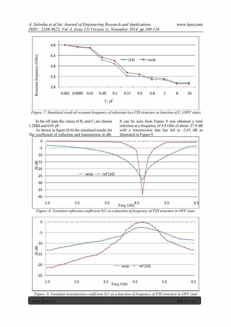
Figure .7. Simulated result of resonant frequency of substrate less FSS structure as function of C j (OFF state)
In the off state the values of R j and C j are chosen
1.2MΩ and 0.01 pF.
As shown in figure (8-9) the simulated results for
The coefficient of reflection and transmission in dB.
It can be seen from Figure 8 was obtained a total
refection at a frequency of 4.8 GHz of about -27.9 dB
with a transmission that has led to -2.63 dB as
illustrated in Figure 9.
Figure .8. Variation reflection coefficient S11 as a function of frequency of FSS structure in OFF state.
Figure .9. Variation transmission coefficient S11 as a function of frequency of FSS structure in OFF state
2.8
3.3
3.8
4.3
4.8
0.001 0.0085 0.01 0.09 0.1 0.57 0.6 0.8 1 8 10
[14] wcip
R e s o n a n t f r e q u e n c y ( G H z
)
C j pF
-40
-35
-30
-25
-20
-15
-10
-5
0
1.5 2.5 3.5 4.5 5.5 6.5
wcip ref [10]
| S | d B
Freq. GHz
-25
-20
-15
-10
-5
0
1.5 2.5 3.5 4.5 5.5 6.5
wcip ref [10]
| S | d B
Freq. GHz
8/10/2019 Characterization Of Switchable And Multilayered FSS Circuits Using The WCIP Method
http://slidepdf.com/reader/full/characterization-of-switchable-and-multilayered-fss-circuits-using-the-wcip 7/8
A. Salouha et al Int. Journal of Engineering Research and Applications www.ijera.com ISSN : 2248-9622, Vol. 4, Issue 11( Version 1), November 2014, pp.109-116
www.ijera.com 115 | P a g e
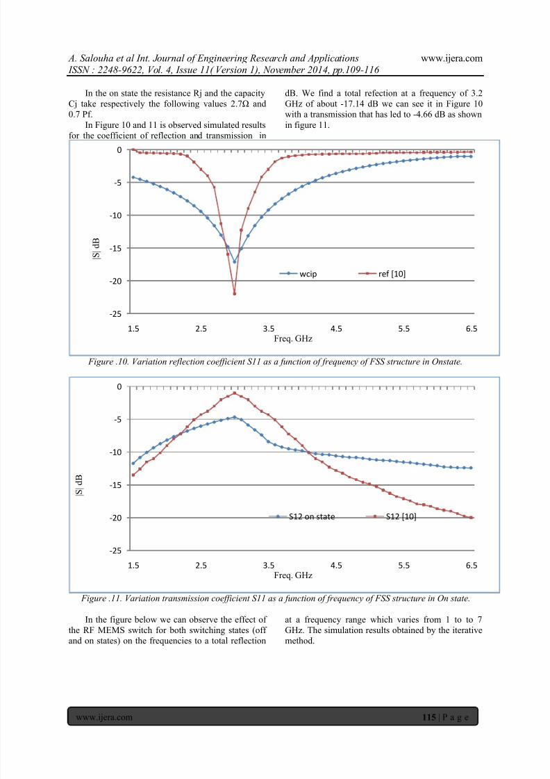
In the on state the resistance Rj and the capacity
Cj take respectively the following values 2.7Ω and
0.7 Pf.
In Figure 10 and 11 is observed simulated results
for the coefficient of reflection and transmission in
dB. We find a total refection at a frequency of 3.2
GHz of about -17.14 dB we can see it in Figure 10
with a transmission that has led to -4.66 dB as shown
in figure 11.
Figure .10. Variation reflection coefficient S11 as a function of frequency of FSS structure in Onstate.
Figure .11. Variation transmission coefficient S11 as a function of frequency of FSS structure in On state.
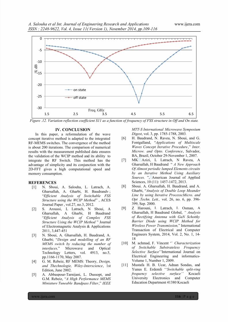
In the figure below we can observe the effect of
the RF MEMS switch for both switching states (off
and on states) on the frequencies to a total reflection
at a frequency range which varies from 1 to to 7
GHz. The simulation results obtained by the iterative
method.
-25
-20
-15
-10
-5
0
1.5 2.5 3.5 4.5 5.5 6.5
wcip ref [10]
| S | d B
Freq. GHz
-25
-20
-15
-10
-5
0
1.5 2.5 3.5 4.5 5.5 6.5
S12 on state S12 [10]
| S | d B
Freq. GHz
8/10/2019 Characterization Of Switchable And Multilayered FSS Circuits Using The WCIP Method
http://slidepdf.com/reader/full/characterization-of-switchable-and-multilayered-fss-circuits-using-the-wcip 8/8
A. Salouha et al Int. Journal of Engineering Research and Applications www.ijera.com ISSN : 2248-9622, Vol. 4, Issue 11( Version 1), November 2014, pp.109-116
www.ijera.com 116 | P a g e
Figure .12. Variation reflection coefficient S11 as a function of frequency of FSS structure in Off and On state.
IV. CONCLUSIONIn this paper, a reformulation of the wave
concept iterative method is adapted to the integrated
RF-MEMS switches. The convergence of the method
is about 200 iterations. The comparison of numerical
results with the measurement published data ensures
the validation of the WCIP method and its ability to
integrate the RF Switch. This method has the
advantage of simplicity and its conjunction with the
2D-FFT gives a high computational speed andmemory consumption.
REFERENCES[1] N. Sboui, A. Salouha, L. Latrach, A.
Gharsallah, A. Gharbi, H. Baudrandv ;
“ Efficient Analysis of Switchable FSSStructure using the WCIP Method ” , ACES
Journal Paper , vol.27, no.3, 2012.
[2] S. Aroussi, L Latrach, N Sboui, A
Gharsallah, A Gharbi, H Baudrand
“ Efficient Analysis of Complex FSS
Structure Using the WCIP Method ” Journal
of Electromagnetic Analysis & Applications2011, 3,447-451
[3] N. Sboui, A. Gharsallah, H. Baudrand, A.
Gharbi; “ Design and modelling of an RF
MEMS switch by reducing the number of
interfaces,” Microwave and OpticalTechnology Letters, vol. 4913, no.5,
pp.1166-1170, May 2007.
[4] G. M. Rebeiz, RF MEMS: Theory, Design,
and Thechnologie, Wiley-Interscience, 1st
Edition, June 2002.
[5] A. Abbaspour-Tarnijani, L. Dussopt, andG.M. Rebeiz, “ A High Performance MEMS
Miniature Tuneable Bandpass Filter ,” IEEE
MTT-S International Microwave Symposium
Digest , vol. 3, pp. 1785-1788, 2003.
[6] H. Baudrand, N. Raveu, N. Sboui, and G.
Fontgalland, “ Applications of Multiscale
Waves Concept Iterative Procedure,” Inter.
Microw. and Opto. Conference, Salvador,
BA, Brazil, October 29-November 1, 2007.
[7] MK Azizi, L Latrach, N Raveu, A
Gharsallah, H Baudrand “ A New Approach
Of Almost periodic lumped Elements circuitsby an Iterative Method Using Auxiliary
Sources. ”, American Journal of Applied
Sciences, 10 (11): 1457-1472, 2013.
[8] Sboui. A. Gharsallah, H. Baudrand, and A.
Gharbi, “ Analysis of Double Loop Meander
Line by using Iterative ProcesscMicro. andOpt .Techn. Lett., vol. 26, no. 6, pp. 396-
399, Sep. 2000.
[9] Z Harouni, L Latrach, L Osman, A
Gharsallah, H Baudrand Global, “ Analysis
of Rectifying Antenna with GaN Schottky Barrier Diode using WCIP Method for
Wireless Power Transmission,” InternationalTransaction of Electrical and Computer
Engineers System, 2014, Vol. 2, No. 1, 14-
18
[10] M. achmad, F. Vincent „‟ Characterizationof Switchable Substrateless Frequency
Selective Surface‟‟International Journal on
Electrical Engineering and informatics-
Volume 1, Number 1, 2009.
[11] Mustafa H. B. Ucar, Adnan Sondas, and
Yunus E. Erdemli „„Switchable split-ring frequency selective surface’’ Kocaeli
University Electronics and Computer
Education Department 41380 Kocaeli
-30
-25
-20
-15
-10
-5
0
1.5 2.5 3.5 4.5 5.5 6.5
on state
off state
| S | d B
Freq. GHz