Embed Size (px)
Citation preview

1
Characterization of Silicon Photomultipliers fornEXO
I. Ostrovskiy, F. Retiere, D. Auty, J. Dalmasson, T. Didberidze, R. DeVoe, G. Gratta, L. Huth, L. James,L. Lupin-Jimenez, N. Ohmart, A. Piepke
Abstract—Silicon Photomultipliers (SiPMs) are attractive can-didates for light detectors for next generation liquid xenondouble-beta decay experiments, like nEXO (next Enriched XenonObservatory). In this paper we discuss the requirements thatthe SiPMs must satisfy in order to be suitable for nEXO andsimilar experiments, describe the two test setups operated by thenEXO collaboration, and present the results of characterizationof SiPMs from several vendors. In particular, we find that thephoton detection efficiency at the peak of xenon scintillation lightemission (175-178 nm) approaches the nEXO requirements fortested FBK and Hamamatsu devices. Additionally, the nEXOcollaboration performed radio-assay of several grams of bareFBK devices using neutron activation analysis, indicating levels of40K, 232Th, and 238U of the order of <0.15, (6.9·10−4 - 1.3·10−2),and <0.11 mBq/kg, respectively.
Index Terms—silicon photomultipliers, xenon detectors, pho-todetectors
I. INTRODUCTION
SEARCH for neutrinoless double-beta decay (DBD) isan active field of research with important implications
for nuclear and particle physics. nEXO is a planned 5-tonliquid xenon detector aimed to probe the effective Majorananeutrino mass in the inverted mass hierarchy region. nEXObenefits from experience gained with the successful EXO-200detector [1], which utilizes ∼200 kg of liquid xenon kept at anominal pressure of '147 kPa and a temperature of '167K. To achieve maximum sensitivity, the nEXO detector isrequired to have an energy resolution of σE
E ∼1% at 2.458MeV [2] (Q value of DBD in 136Xe). The experiment furtherneeds to achieve unprecedented levels of background in orderto be able to detect a weak effect. A detector containing thelargest physically or fiscally feasible amount of the decayingsubstance maximizes the decay rate.
In the EXO-200 experiment, the resolution is limited by thenoise in the photodetector channels. EXO-200 uses Large AreaAvalanche Photo-diodes (LAAPDs) operated at a gain of ∼200and an equivalent noise of ∼10 photoelectrons per readout
I. Ostrovskiy, R. DeVoe, G Gratta, and L. Lupin-Jimenez are with PhysicsDepartment, Stanford University, Stanford, California 94305 USA. (e-mail:[email protected])
F. Retiere, L. Huth, L. James, and N. Ohmert are with TRIUMF, Vancouver,British Columbia V6T 2A3, Canada
D. Auty, T. Didberidze, and A. Piepke, are with Department of Physics andAstronomy, University of Alabama, Tuscaloosa, Alabama 35487, USA
D. Auty is now at University of Alberta, Edmonton, Alberta, CanadaJ. Dalmasson is with Physics Department, University of Massachusetts,
Amherst, Massachusetts 01003, USAThis work was supported by the U.S. Department of Energy Offices of
High Energy and Nuclear Physics, Natural Sciences and Engineering ResearchCouncil of Canada, and TRIUMF Science Technology Department.
channel. Alternative light sensors that are gaining popularity inrecent years are Silicon Photomultipliers (SiPMs). SiPMs arephotodetectors under investigation for use in nEXO becauseof their high gain and expected low radioactive content. Dueto large gains, on the order of 106, SiPMs have the potentialto yield much higher signal-to-noise ratios, to the point thatit is not unreasonable to expect noise below 1 photoelectronequivalent. SiPM devices that are currently available need toexhibit the following characteristics:
1) High photon detection efficiency (PDE) at 175-178 nm(peak of Xe scintillation light emission): The aim for overallefficiency for detecting the scintillation photons produced inliquid Xenon is 10%. Simulations show that this efficiencyis achievable if the sensors’ PDE is at least 15%. Note thatthis includes loss of light due to reflection off the SiPM’ssurface, which is large (∼50%) when SiPMs are submerged inliquid xenon due to the large mismatch in indices of refractionat 175 nm between silicon (n ∼ 0.8 + 1.9i [3]) and xenon(n = 1.7 [4]). As a first step of the photodetector R&Dwe perform measurements in vacuum in order to more easilytest different photodetectors. Once devices passing our firstlevel tests (described in this paper) have been identified, theirfunctionality in liquid xenon will be verified and reflectivityof the photodetectors will be measured as a function of angle.
2) High Radiopurity: We demand that the content of thephotodetectors has to be a sub-dominant contributor to thebackground budget, compared to other sources (e.g., thedetector vessel). As a guide, we currently require that thephotodetectors contain no more than ∼ppt levels of 238U and232Th, which corresponds to specific activities on the order of∼10 µBq/kg. In practice, any solution that involves packagingmaterial added to the bare device, especially ceramic, isdisadvantageous, compared to using bare detectors.
3) Small values of photodetector nuisance parameters:Dark noise pulses start contributing to the dead time if theirrate exceeds ∼200 MHz when summing over all SiPMs.Assuming 4 m2 photo-coverage, the dark noise rate limit is50 MHz/m2 or 50 Hz/mm2. This dark noise rate is to beachieved at liquid xenon temperatures. Correlated avalanchesin SiPMs are caused by cross-talk (CT) and after-pulses (AP).They start contributing to the energy resolution if the fractionof additional (correlated) avalanches created by one avalancheexceeds 0.2.
4) Good photodetector electrical properties: Scintillationlight is emitted isotropically, hence the spatial distributionof the light does not need to be sampled finely. Decreasingthe number of readout channels also allows us to minimize
arX
iv:1
502.
0783
7v2
[ph
ysic
s.in
s-de
t] 6
Jul
201
5
2
TABLE ISUMMARY OF SIPM PARAMETERS REQUIRED BY NEXO. PARAMETERS IN
ITALIC ARE PREFERABLE, BUT NOT MANDATORY.
Parameter ValuePhoto-detection efficiency at 175-178 nm(without anti-reflective coating in gas/vacuum)
≥15%
Radio-purity:232Th and 238U <10 µBq/kg
Dark noise rate at -100◦C ≤50 Hz/mm2
After-pulse and cross-talk probability ≤20%
Single photodetector active area ≥1 cm2
Gain fluctuations and electronic noise ≤0.1 p.e.
Single photon timing resolution <10 ns
the number of required feedthroughs. The size of singlephotodetector elements should be at least 1×1 cm2 (thecurrent baseline design for nEXO assumes a unit readout cellof 5 cm2). Larger areas, up to 20×20 cm2, are preferablebut are limited by the electronics noise that scales with thecapacitance per channel. Therefore, low capacitance per unitarea is desirable (e.g. <50 pF/mm2) [5].
5) Several ns timing resolution: Good timing resolutionis not essential for nEXO. Several ns single photon timingresolution would be sufficient. Nevertheless, single photontiming resolution might prove useful for other applications,by allowing better pulse shape discrimination and positionreconstruction with light only using time of flight.
6) Compatibility with liquid xenon: Very long electron lifetime (∼10 ms) must be achieved in nEXO, due to the long driftdistances in a large detector, which requires very low levels ofelectron absorbing contaminants. Therefore, the photodetectorsand associated ancillary mechanical and electrical interfaceswill have to be tested in liquid xenon together with the passiveoptical elements to ensure acceptable levels of out-gassing.Furthermore, operation of the complete light detection systemmust be demonstrated in liquid xenon. In practice, any solutionthat involves wavelength shifters, which are commonly usedto enhance PDE in the VUV region, poses additional risks,compared to the operation of bare devices.
Table I summarizes the required SiPM parameters.The challenges listed above are addressed in close collab-
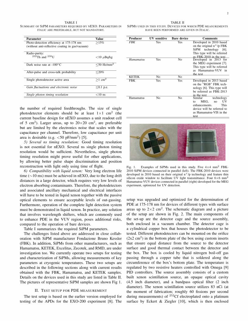
oration with SiPM manufacturer Fondazione Bruno Kessler(FBK). In addition, SiPMs from other manufacturers, such asHamamatsu, KETEK, Excelitas, Zecotek, and RMD, are underinvestigation too. We currently operate two setups for testingand characterization of SiPMs, allowing measurements of keyparameters at cryogenic temperatures. These two setups aredescribed in the following sections along with current resultsobtained with the FBK, Hamamatsu, and KETEK samples.Details on the devices used in this study are listed in Table II.The pictures of representative SiPM samples are shown Fig 1.
II. TEST SETUP FOR PDE MEASUREMENT
The test setup is based on the earlier version employed fortesting of the APDs for the EXO-200 experiment [8]. The
TABLE IISIPMS USED IN THIS STUDY. DEVICES FOR WHICH PDE MEASUREMENTS
HAVE BEEN PERFORMED ARE GIVEN IN ITALIC.
Producer UV sensitive Bare device CommentsFBK Yes Yes Developed in 2010 based
on the original n+/p FBKSiPM technology [6].This type will be referredas FBK-2010 in the text
Hamamatsu Yes No Developed in 2013 forthe MEG experiment [7].This type will be referredas Hamamatsu-VUV inthe text
KETEK No NoFBK Yes Yes Developed in 2013 based
on the ”RGB” FBK tech-nology [6]. This type willbe referred as FBK-2013in the text
Hamamatsu No No Similar technologyto MEG, no UVenhancements. Thisdevice will be referred toas Hamamatsu-VIS in thetext
Fig. 1. Examples of SiPMs used in this study. Five 4×4 mm2 FBK-2010 SiPM devices connected in parallel (left). The FBK-2010 devices weredeveloped in 2010 based on their original n+/p technology and feature thinsilicon oxide window to facilitate UV light transmittance. Four 6×6 mm2
Hamamatsu-VUV devices connected in parallel (right) developed for the MEGexperiment, optimized for UV detection.
setup was upgraded and optimized for the determination ofPDE at 175-178 nm for devices of different types with surfaceareas up to 2×2 cm2. The schematic diagram and a pictureof the setup are shown in Fig. 2. The main components ofthe set-up are the detector cage and the source assembly,both enclosed in a vacuum chamber. The detector cage isa cylindrical copper box that houses the photodetector to betested. Different photodetectors can be mounted on the orifice(2x2 cm2) in the bottom plate of the box using custom insertsthat ensure equal distance from the source to the detectorsurface and good thermal contact between the detector andthe box. The box is cooled by liquid nitrogen boil-off gaspassing through a copper tube that is soldered along thecircumference of the box’s bottom plate. The temperature isregulated by two resistive heaters controlled with Omega [9]PID controllers. The source assembly consists of a custombuilt xenon scintillation source, an opaque optical cavity(4.5 inch diameter), and a bandpass optical filter (2 inchdiameter). The xenon scintillation source utilizes 83 nCi (atthe moment of fabrication; roughly 60 fissions per secondduring measurements) of 252Cf electroplated onto a platinumsurface by Eckert & Ziegler [10], which is then enclosed

3
�
����������AB
�CDDAE�FC�
�CC����������
�A�A��CE�FC�
������D�AEA�����AE��C��B�C���
�C�E�A
�C�E�A��BBA��
Fig. 2. A cross-sectional view of the CAD model (left) and a photograph(right) of the Stanford test setup.
in a miniature chamber filled with xenon gas at ∼1 barpressure. A similar source based on 241Am was also fabricated,but not used routinely. The use of a 252Cf-fission sourcehas the advantage of order of magnitude larger scintillationlight output, compared to an alpha source (we estimate thescintillation flux at the bottom plate of the detector box to be∼2 photons/mm2 per fission) . A picture of one of the twoxenon scintillation sources is shown in Fig. 3. Additionally, ablue LED is installed inside the vacuum chamber and can beused as an alternative light source of varying intensity. The
�
Fig. 3. The custom-built xenon scintillation source.
optical cavity confines the xenon scintillation light emitted bythe source, avoiding parasitic reflections off aluminum andTeflon surfaces inside the vacuum chamber. It is implementedas a Teflon (PTFE) sphere with two concentric openings for thesource at the bottom and the detector at the top, approximately2 inch in diameter each. Fitted at the top sphere’s opening, 2-3mm in front of the detector’s surface, is the Pelham Research
Optical [11] bandpass filter. The filter’s transmission curveis centered at 180 nm (40 nm FWHM) to avoid bias due topotential re-emission of Teflon into longer wavelengths andcontamination by the sub-dominant infra-red component ofxenon scintillation.
A. PDE measurement
Signals from the photodetectors are routed from the detectorcage via a vacuum feed-through using low capacitance flexiblecables and amplified by a Cremat [12] charge sensitive pream-plifier and a Gaussian shaper. The signals are then digitizedby a National Instruments digitizer. A LabView based dataacquisition program collects waveforms in either continuousor triggered mode, which are then reconstructed and analyzedusing ROOT [13] based custom software. Fig. 4 shows anexample spectrum obtained with the FBK-2010 SiPM deviceand the setup described above.
To provide an absolute PDE reference we use a HamamatsuR9875P photomultiplier tube (PMT) with calibrated quantumefficiency at 175 nm. The reference PMT has a synthetic silicawindow, an outer diameter of 15.9 mm (Cs-Te photocathodeeffective diameter 8 mm) and is mounted in the detector cageat the same position as other photodetectors. The PMT isoperated at room temperature, biased to the recommendedplateau voltage (1190 V), and its gain is calibrated with lowintensity LED light pulses. The PDE of the SiPM devices isthen extracted by comparing their responses (specifically, the252Cf spontaneous fission peak position, expressed in numberof photoelectrons per unit area, which is typically in the rangeof 0.2 - 0.4 photoelectrons per mm2) to that of the referencePMT.
���������A�B�C�DEDF
Fig. 4. Charge spectrum recorded with the FBK-2010 SiPM device exposedto xenon scintillation light excited by the 252Cf (black line) and 241Am(red hatched line) sources. The dark noise distribution is shown as blue filledregion. Peaks from alpha and fission decays are visible. 252Cf undergoes bothalpha and spontaneous fission decays, while 242Am only undergoes alphadecay.
An important part of the measurement is the parasitic chargecorrection applied to the SiPM devices. The total amount ofobserved charge is biased towards larger values, predominantlydue to the contribution of correlated avalanches (typicallydominated by cross-talk, with addition of after-pulses). Thecorrection is determined from separate estimates of the ratesof cross-talk and after-pulsing. Note that it is also possible

4
for dark hits to contribute to the bias, but in practice thiscontribution is typically negligible.
For the PDE measurement, several sources of errors aretaken into account:
1) Raw charge spectrum calibration: The gain calibrationis applied for each value of the over-voltage (defined as theexcess bias beyond the breakdown voltage of the device) toconvert the raw charge into the number of photoelectrons perunit area. The over-voltage value itself depends on the value ofthe breakdown voltage, which is determined by extrapolatingthe gain-voltage dependence to zero gain using a linear fit. Therelative SiPM gain at each over-voltage is extracted from thedark charge distribution. While SiPMs are known to typicallyhave very good single photoelectron (s.p.e.) resolution, thedevices measured here have large readout areas (∼1 cm2, con-nected in parallel), which leads to increased peak widths due toa) an increased readout noise and b) an increased rate of pulsereconstruction errors related to pile-up. In practice, only singleor double photoelectron peaks could be reliably resolved. Thegain is then determined by fitting the dark pulse distributionwith a function representing pedestal and each photoelectronpeak by a Gaussian. Fig. 5 shows the distribution of randompulses occurring in the absence of light (dark pulses) obtainedwith the FBK-2010 device. The fit error on the s.p.e. equivalentcharge is typically on the order of 0.5-1.5%. This error also
���������A�B�C�DEDF
Fig. 5. Dark pulse charge distribution obtained with the FBK-2010 device.Data shown as dots. The red solid line is a two Gaussian fit to the pedestaland single photoelectron peaks.
affects the determination of the breakdown voltage and ispropagated by the linear fit of the gain-voltage dependence.Note that the breakdown voltage error (typically, ∼0.1-0.2V) could be straightforwardly translated into an additionalerror on the gain at a given voltage, thus decoupling thisuncertainty from the inherent dependence of the PDE onover-voltage. Given the linear dependence of the gain onthe over-voltage, the ±0.2 V uncertainty on the breakdownvoltage translates into ∼4% gain error for the FBK-2010and ∼0.6% for Hamamatsu-VUV devices, averaged over usedover-voltages. Similarly, the imperfect temperature stabilityof the setup (typical RMS ∼0.2-0.3◦C) also contributes tothe gain error via the over-voltage variation. To evaluate thiscontribution we determine the temperature dependence of theover-voltage. The FBK-2010 devices show approximately 8-10 V breakdown voltage variation between room temperatureand -104◦C. The rate of change of the breakdown voltage withtemperature is itself a function of temperature, so we measure
it close to the value of interest (Fig. 6) and find a slope of ∼50mV/◦C near -104◦C. Conservatively assuming 1◦C variation,the gain uncertainty contribution is ∼1%. In total, a 5% error
�
���������
�� A� ��BCB�
Fig. 6. SiPM gain as a function of bias voltage at -104◦C (circles) and-114◦C (squares), measured with the FBK-2010 device. The blue lines arelinear fits (the best-fit parameters are shown on the plot). Statistical error onindividual gain measurements is ∼1%, which is comparable to the markersize.
on the charge calibration is estimated.2) Solid angle: The setup is designed such that the de-
tectors being tested and the reference PMT are located atthe same distance from the source and their surface areassubtend a small fraction of one steradian (<0.03 sr). In onecase (Hamamatsu-VUV) a non-standard detector holder had tobe used, which resulted in an offset of approximately 3 mmfor this detector relative to others. This is accounted for by anappropriate correction. In all cases, the position is known to1-2 mm that, given the distance between the source and thedetectors, translates into ≈3% uncertainty on the light flux.
3) Light source temperature dependence: Due to imperfectthermal isolation of the source assembly from the detectorcage, the source temperature was observed to gradually de-crease over time after the detector cage is cooled down andmaintained at the liquid xenon temperature (∼104◦C). Thesource temperature decreases ∼4◦C/hr from room temperatureduring the first two hours following the cool down. Coincidentwith the temperature decrease, the fission peak position wasfound to increase at the rate of ∼4-5%/hr, while the SiPMgain remained constant, confirming that the SiPM remained inthermal equilibrium with the detector cage (Fig. 7). Conser-vatively assuming that measurements with different detectorsare performed two hours apart after cool down, we assign a10% error to this effect.
4) Fission peak equivalent charge: The fission peak equiva-lent charge is determined by a Gaussian fit (Fig. 12). A typicalfit error is <1%. While the resolution of a single device is toopoor to observe any potential structures in the fission energyspectrum, the Gaussian provides a good fit, and its mean ismuch farther separated from the background than the alphapeak, which makes it a good variable to compare efficiencyof different devices.
5) PMT absolute reference: The total error budget is cur-rently dominated by the uncertainty on the absolute PDEreference, which in our case is provided by the reference

5
�
����������
�AB�CDE�F�D���A����
����������
�A����A����
Fig. 7. Drift of the fission peak position over time (top) observed witha SiPM held at -104◦C. The temperature of the scintillation source wasfound to decrease by ∼4◦C/hr from room temperature after the cool downof the detector cage. The SiPM gain (bottom) remained constant during themeasurement, confirming that the SiPM was in thermal equilibrium with thedetector cage.
PMT described earlier. The PDE of a PMT can be expressedas a product of quantum and collection efficiencies. Thequantum efficiency depends on the wavelength of the detectedlight and was measured by Hamamatsu to be 20.1% at 175nm for the PMT used (the calibration uncertainty is ∼2%).The collection efficiency depends on the voltage differencebetween the photocathode and the first dynode. It typicallyvaries from 80% to 100% [14, Fig.4-12], but for the PMTtype used in this study was reported by Hamamatsu to be70%. Hamamatsu did not provide a reference curve for theparticular tube we used, so we approximate the collectionefficiency by 70±10%. The central value is suggested byHamamatsu, while the full variation from [14, Fig.4-12] isused as an uncertainty. The tube to tube variability is assumednegligible. An additional uncertainty arises from imperfectlyknown single photoelectron gain. The PMT gain is typicallycalibrated with a very low intensity LED source, such thatthe charge spectrum obtained by triggering on the LED’sdriver pulse is dominated by pedestal and single photoelectronsevents (the mean Poisson photoelectron rate is ∼0.1). Thisway the contamination of multiple photoelectron events isnegligible and the gain can be determined typically withsub-percent uncertainty. Due to the poor peak-to-valley ratioobserved for the used PMT, we calibrated the gain using largerlight intensity (with mean Poisson rates of ∼2-3.5), such thatthe centroid of the resulting charge distribution is more clearlyseparated from the pedestal peak. A substantial remainingprobability of the pedestal (i.e., zero photoelectron) eventsallows us to determine the mean Poisson rate, which providesthe expected fractions of single-, double-, etc., photoelectronevents. The fraction of the pedestal events is determined by aGaussian fit, with the peak width and position fixed to the val-ues obtained in the dark conditions. No loss of pedestal event
is expected, given the externally triggered threshold-less dataacquisition. A 10% error on the Poisson rate is conservativelyassumed. The single photoelectron gain is then determinedfrom a multi-photoelectron fit (Fig. 8). The stability of the fitwas checked by repeating the calibration procedure at differentPMT voltages, recovering an exponential dependence of thegain. The gain calibration was found to vary within 6% if thelight intensity was changed such that the mean Poisson ratechanged by a factor of ∼2. We round the quadratic sum ofthe three contributions up to 19% overall uncertainty on thePMT reference.
�
���������ABC��DEF
Fig. 8. Distribution of peak amplitudes (black dots) obtained with thereference PMT exposed to low intensity LED light. The distribution is fit bya function (blue solid line) representing the sum of the pedestal and severalphotoelectron peaks. The mean Poisson rate (∼2) is determined by the fractionof pedestal events.
6) Parasitic charge correction: Parasitic charge correctionsfor FBK-2010 and Hamamatsu-VUV devices are taken frompublished data ( [6] for FBK-2010 and [7] for Hamamatsu-VUV). In both cases, the correction takes into account themain sources of correlated noise: cross-talk and after-pulsing.The probability of either, as is pointed out in [6], does notchange with the incoming photon flux, or wavelength. FBKclaims very small probability of correlated avalanches for thedevices based on their original technology, even at high over-voltages (∼5% at 5V over-voltage). For the Hamamatsu-VUVdevices, on the other hand, the contribution is substantiallylarger (∼30% at 2V over-voltage). Neither publication ex-plicitly states uncertainties on the measured correlated noisecontributions to the total charge. In the case of Hamamatsu-VUV, the ±(2-4) abs.% spread observed in the correctionvalues at each over-voltage for different devices is used asan estimate of the uncertainty. In the case of the FBK-2010devices, we performed a partial cross-check by evaluatingthe probability of cross-talk (which is the dominant sourceof parasitic charge) in situ from the ratio of single- tomulti-photon signals in dark conditions. The dependence ofthe observed cross-talk probability on over-voltage (Fig. 9)agrees with the parasitic charge dependence on over-voltageextracted from [6] to within 1-2 abs.%. Given the values of therequired corrections, these differences translate into ∼6 and∼2 rel.% error on the PDE for Hamamatsu-VUV and FBK-2010 devices, respectively. We conservatively use the largervalue for all measurements.

6
���������A�BCDE
F�������B����������
Fig. 9. Probability of cross-talk, estimated from the ratio of single- to multi-photon events, as a function of over-voltage for a FBK-2010 device.
TABLE IIISYSTEMATIC ERRORS OF THE PDE MEASUREMENT. ITEMS SHOWN IN
ITALIC CORRESPONDS TO THE SOURCES OF ERROR CORRELATED AMONGDIFFERENT MEASURED DEVICES.
Source of error Value, %PMT absolute reference 19Light flux temperature dependence 10Parasitic charge correction 6SiPM charge calibration 5Solid angle 3Fission peak equivalent charge 1Total ∼23
Table III summarizes the systematic error budget. Itemsshown in italic correspond to errors correlated among differentmeasured devices. The total error budget of the absoluteefficiency measurement is estimated at ∼20%. The relativeperformance of Hamamatsu-VUV and FBK-2010 SiPM de-vices is determined more accurately (∼13%, dominated bythe light flux temperature dependence and parasitic chargecorrection).
III. TEST SETUP FOR CROSS-TALK AND AFTER-PULSINGMEASUREMENT
The dark noise, after-pulsing rates, and the cross-talkprobability were measured in a test setup at TRIUMF. Thesetup was designed to rapidly measure the performances ofphotodetectors in conditions as close as possible to nEXO. Thephotodetectors were mounted on printed circuit boards thatattach to a INSTEC HCP302 cooling chuck whose temperatureis regulated by the combination of liquid nitrogen boil offgas running and a heater embedded in the chuck. The coolingchuck can easily reach -110◦C even when surrounded by warmgas. The whole setup is enclosed in a light tight box filledwith nitrogen gas whose purpose is to prevent condensationand to allow the propagation of 175 nm light. No lightsources were used, however, for the data reported in this paper.All data reported in this paper were taken at -100◦C coldchuck temperature. The photodetector temperature tracked thetemperature of the chuck within a few degrees depending onthe photodetector package.
Due to several constraints, different devices were testedat TRIUMF and at Stanford (see Table II). The devicestested at TRIUMF were manufactured by KETEK, FBK and
Hamamatsu. The KETEK devices are 3×3mm2, 50µm pitchSiPM. The FBK devices, FBK-2013, are 1×1mm2 secondgeneration SiPMs. The Hamamatsu devices, Hamamatsu-VIS,are 3×3mm2, 50µm pitch non-VUV sensitive SiPMs (alsocalled by Hamamatsu Multi-Pixel Photon Counters, MPPCs)whose nuisance parameters are expected to be very similarto the MPPCs developed for the MEG experiment. The per-formances of these devices were measured at about 5V over-voltage for the KETEK and FBK-2013 devices, and 2.5V forthe Hamamatsu-VIS MPPC.
Signals from the photodetectors were amplified by a fac-tor 100 using two Mini-Circuits MAR6-SM+ amplifiers inseries [15]. A 50 Ohm coaxial cable was used to connect thephotodetector to the amplifier board. The MAR6-SM+ are veryfast amplifiers that allow measuring the photodetector pulseshape with minimum distortions. Signals from the amplifierboard were readout by a Lecroy Waverunner oscilloscope.Waveforms were recorded by triggering on signals above theelectronics noise. The waveforms were 10 µs long with thesampling rate limited to 1 Giga-sample per second (GS/s) asa compromise between timing resolution and data processingspeed. Examples of digitized waveforms are shown on Fig. 10.
Dark noise and after-pulse rates are measured by compilingthe distribution of the time differences between the triggerpulse and the next pulse. At -100◦C most of the waveformshave only one pulse and the timing difference is calculatedusing the time stamp of each waveform provided by theoscilloscope. Unfortunately, the oscilloscope has a dead timeof 4 µs after each waveform that has to be accounted for whencharacterizing the timing distribution. After-pulses can occurwithin the same waveform as the trigger pulse. The waveformsare analyzed as follows: 1) a pulse finder identifies pulseswhose shape and amplitude are inconsistent with electronicsnoise, 2) pulses are fitted using an analytical template repre-senting the pulse shape by minimizing an approximate chi-square that is calculated using the single bin noise (about 1mV), 3) if the chi-square is larger than a certain threshold thepulses are refitted by adding additional pulses until either thechi-square falls below the threshold or the chi-square does notimprove significantly or the number of added pulses reachesa maximum of 5. The third procedure allows identifyingpartially overlapping pulses. The pulse template that fits alltested SiPMs is the convolution of a Gaussian distribution withone or two exponential functions.The pulse polarity is negativestarting with a fast fall time and followed by a slower rise time.The fall time is calculated as the time it takes to for the pulse togo from 10% to 90%. The rising part of the pulse is describedby exponential functions and parametrized by the exponentialtime constants. Two exponentials are typically needed whenthe parasitic capacitance across the quenching resistor is largerthan a few femtofarad.
The obtained distribution of the time differences betweenthe trigger pulse and the next pulse is fit by a functionto extract dark noise and after-pulse rates. The function isconstructed assuming that both dark noise and after-pulsingaffect the time difference distribution as described in [16].The fit function is expanded to account for several featuresthat were either ignored or that are specific to the nEXO

7
Time (sec)-0.05 0 0.05 0.1 0.15 0.2 0.25 0.3
-610×
Vo
ltag
e (V
)
0.09
0.1
0.11
0.12
0.13
0.14
0.15
KETEK
Time (sec)-0.05 0 0.05 0.1 0.15 0.2 0.25 0.3
-610×
Vo
ltag
e (V
)
0.4
0.6
0.8
1
1.2
FBK-2013
Time (sec)-0.05 0 0.05 0.1 0.15 0.2 0.25 0.3
-610×
Vo
ltag
e (V
)
0.09
0.1
0.11
0.12
0.13
Hamamatsu-VIS
Fig. 10. Examples of single avalanche pulse waveforms for a KETEK (left), FBK-2013 (middle), and Hamamatsu-VIS (right) SiPMs devices with the fitfunction superimposed. The function fits the prompt peak but it is truncated when displayed.
setup. Recovery was ignored in [16], but it has a noticeableimpact on the probability of generating and detecting after-pulsing. Indeed, the probability of triggering an avalanche ofany kind depends on the over-voltage and our fit functionassumes somewhat arbitrarily that it scales linearly with over-voltage, hence it follows the exponential recovery function.In the early part of the recovery, our pulse finder algorithmmay miss pulses if their amplitudes are too small. We modelthis process by introducing a dead time that depends on therecovery time constant (150, 100, and 8 ns for the KETEK,FBK-2013 and Hamamatsu-VIS SiPMs, respectively). Ourfunction ignores delayed cross-talk that do not suffer fromrecovery because their occurrence rate is relatively small.They could be included at the cost of yet another parameteraccounting for delayed cross-talk probability. Our functionalso includes the oscilloscope deadtime between 8.5 and 12.5µs. The complete function shown in (1) combines the functionsshown in (III), (3), (4), and (5). The dark noise rate is handledby a single rate parameter, RD. Each after-pulsing probabilityis parameterized by an exponential function with two freeparameters - a time constant, τAi , and a probability, PAi .The after-pulsing indexes are omitted in (III) and (3) forsimplicity. After-pulsing is approximated using a probabilityrather than using Poisson statistics for simplicity as well.This approximation is justified as long as all after-pulsingprobabilities are low. τr is the recovery time constant, trd,tsds, and tsde are the recovery deadtime, oscilloscope startdeadtime, and oscilloscope end deadtime respectively.
Ptotal(t) = PD(t)
i<nA∏i=0
PAi(t)
+ PD(t)
i<nA∑i=0
[PAi(t)
j<nA & j 6=i∏j=0
PAj (t)] (1)
PA(t) =
{0, if t<trd or tsds<t<tsde1−e
− tτr
τAe− tτA , otherwise
(2)
PA(t) =
0, if t≤trde− trdτA +e−
trdλ −e−
tτA −e−
tλ , if trd<t≤tsds
e− trdτA +e−
trdλ −e−
tsdsτAP −e−
tsdsλ , if tsds<t≤tsde
e− trdτA +e−
trdλ −e−
tsdsτA −e−
tsdsλ +
e− tsde
τA +e−tsdeλ −e−
tτA −e−
tλ , if t>tsde
(3)
where λ = (τr + τA)/τr/τA.
PD(t) =
{RDe
−RDt, if t≤tsds0, if tsds<t≤tsdeRDe
−RD(t−tsde+tsds), if t>tsde(4)
PD(t) =
{e−RDt, if t≤tsdse−RDtsds , if tsds<t≤tsdee−RD(t−tsde+tsds), if t>tsde
(5)
The cross-talk probability was inferred by measuring thefraction of single pixel avalanches in the trigger window. Wedefine the cross-talk probability as the probability that a singlepixel avalanche triggers one or more additional avalancheswithin 1 ns of the parent avalanche. The physical mechanismresponsible for cross-talk is the absorption of photons pro-duced in the parent avalanche within the high field region ofneighboring pixels. The same mechanism is known to leadto delayed avalanches, within a few ns up to several µs laterdue to the diffusion of the charge carriers produced by photonabsorption in regions with zero or very small electric field. Byconstruction, we only include prompt cross-talk and such adelayed cross-talk contributes to after-pulsing instead. Indeed,to measure cross-talk we calculate the probability p1 that thetrigger pulse is a single pixel avalanche and we define thecross-talk probability as 1− p1.
IV. RADIO-PURITY MEASUREMENTS
The nEXO group at the University of Alabama investigatedthe radioactivity content of FBK-2013 SiPMs by means ofneutron activation analysis (NAA). Particular attention waspaid to K, U and Th. The radio active decay series of232Th and 238U are a background concern for nEXO. Highenergy gamma-rays, emitted during the decay of Th and Udaughters, can penetrate the detectors interior and contribute

8
TABLE IVPARAMETERS OF THE IMPORTANT γ BACKGROUNDS FOR NEXO [17].
Parent Isotope half-life Important decay Important γ-ray[1·109y] [keV]
40K 1.248± 0.003 40K →40Ar 1460.822±0.006232Th 14.0 ± 0.1 208Tl→208Pb 2614.511 ± 0.10238U 4.468 ± 0.003 214Bi→214Po 2447.70 ± 0.3
to the measured background. Potassium has a lower Q-value,so is not important for the neutrinoless DBD, but it can affectthe accuracy of alternative physics searches. Table IV showsthe half-lives and γ-ray energies for the important nEXObackgrounds. Direct gamma-ray counting of large samplesallows us to measure Th, and U concentrations of a fewhundred ppt. NAA allows for ppt and even sub-ppt sensitivitiesand requires smaller samples, than direct background counting,an important aspect for this study where kg-size samples arehard to obtain. However, the translation of NAA-determinedTh and U concentrations into a background expectation valuerequires assumptions on the chain equilibrium, not requiredfor direct background counting. Three samples obtained fromFBK were activated at the MIT research reactor (MITR) inthree separate beam times. In order to evaluate bulk and notsurface properties of these devices, they were cleaned usingthe techniques described in [18]. However, there were somevariations from the technique described in [18] and what wasdone here. The June 2013 activation sample was soaked forthree days in 0.5M certified low Th/U nitric acid [19]. Duringthe preparation process the TiN backing to the FBK-2013 chipswas lost. To counter the loss of the backing the acid soak wasreduced to 12 h for the following activations. The integralthermal, epi-thermal, and fast fission neutron fluxes at MITRwere determined by activating NIST certified fly ash [20] (anelement cocktail with known composition) and a sample ofTiN. In earlier studies we established that sample port 2PH1(located close to the fuel element) has a high thermal neutronflux of about (4-5)·1013 cm−2s−1 but also a relatively highfast neutron flux of about 3·1012 cm−2s−1. This leads to thecreation of significant Ti-related side activities that interferewith the Th and U analysis. These unwanted side activities aremainly due to the 46Ti(n,p)46Sc and 48Ti(n,p)48Sc reactions.To suppress these backgrounds we activated the last two SiPMsamples in MITRs sample port 1PH1, showing a 230-foldreduced fast neutron flux at the expense of a 6-times lowerthermal neutron flux. We compensated for the lower thermalflux by means of longer exposure times, a viable solutiongiven the relatively long live time of the Th and U activationproducts 233Pa and 239Np. For 1PH1, the fast neutron fluxwas found to be so low, that the fly-ash could not providea definitive measurement. To find the fast-neutron flux asample of TiN was also activated. After receiving the activatedsamples at the University of Alabama they were separatedfrom the activation vials and then weighed to account forsample loss. Time and energy differential counting was thenperformed using two shielded Ge-detectors. The calibration ofthe gamma ray detection efficiency of the Ge detectors wasperformed using an Eckert & Ziegler [10] source solution,
TABLE VLISTING OF THE SAMPLES ANALYZED IN THREE ACTIVATION CAMPAIGNS
AT MITR. WE LIST THE SAMPLES MASSES, MITR SAMPLE PORT, ANDCOUNTING DELAY (AFTER END OF ACTIVATION). THE MAY 2014
ACTIVATION WAS SPLIT INTO TWO TIME SEGMENTS AS THE SAMPLE WASEJECTED EARLY. THIS IS TAKEN INTO ACCOUNT IN THE ANALYSIS.
Activation Port Sample Activation delay inmass [g] length [h] counting [h]
June 2013 2PH1 0.1705 8.00 103May 2014 1PH1 3.5519 81.43 127July 2014 1PH1 3.8906 80.45 33
containing multiple gamma-ray emitters of known activity.The gamma-rays counted by the detector, in form of fullabsorptions peaks, were compared to the known activities toarrive at an energy dependent efficiency curve, described bya fifth degree polynomial fit. For the analysis of the samples,the code described in [18] was used. Briefly, this allows theuse of the full data set and produces a time dependent decaycurve for each isotope. An example of the double differentialenergy and time analysis is shown in Fig. 11. The fittedsample activity at some reference time (N0 in Fig. 11) thensummarizes all γ-peak integrals evaluated at all times in formof a single value. For all sample fits the half lives are fixed totheir tabulated values. The elemental concentrations were theninferred using properly averaged thermal/epi-thermal and fastneutron cross-sections [21]. It was assumed that the relativeisotopic abundances in the samples are given by the naturalterrestrial abundance ratios. Table V shows the details of thethree beam times performed with FBK-2013 chips. For thefirst two activation campaigns, sensitive analyses of K and Uwere hampered by the relatively long delay between end ofirradiation and start of counting.
��������������AB�C�D�ECD�A��F��
Fig. 11. An example for the time dependence fit for 239Np, the blue dots aredata and the red line is the best fit value. The half-life is fixed to its tabulatedvalue (56.54 h), so only the activity at the end of the activation (67+/-1 Bq)is determined by the fit.
V. RESULTS
A. Photon detection efficiency at 175-178 nm
Fig. 12 shows an example of the xenon scintillation spec-trum obtained with the Hamamatsu-VUV device in the Stan-ford setup. The fission fragment peak equivalent charge is

9
TABLE VIPDE RESULTS. NOTE AN ADDITIONAL CORRECTION OF 15% HAS BEEN
ADDED IN THE CASE OF HAMAMATSU-VUV DEVICES, AS DESCRIBED INTHE TEXT. RELATIVE UNCERTAINTY ∼23%.
Device Over-voltage,[V]
Fissionpeak,[p.e./mm2]
Parasiticchargecorrection,[%]
PDE,[%]
Hamamatsu-VUV 1.5 0.135 14.4 7.61.7 0.161 19.2 8.71.9 0.174 24.0 11.02.2 0.269 31.3 13.2
FBK-2010 3 0.064 2.2 3.44 0.110 4.4 5.75 0.147 6.7 7.66 0.187 8.9 9.4
determined with a Gaussian fit. The correction for parasiticcharge is applied based on [7].
Two additional corrections are needed in this particular case.First, the device’s packaging includes a 0.5 mm thick quartzwindow in front of the sensitive area. To compensate forthe finite transmittance of the window, we apply a 10±1%correction [22, Fig.5]. Second, due to specifics of the device’spackaging, the sensitive surface was positioned 3±1 mmfarther away from the light source than other detectors andthe reference PMT. This results in 5.0±1.5% correction forthe smaller solid angle.
Table VI lists fission peak positions, correction values, andPDE numbers at different over-voltages for the measureddevices. All measurements were performed at -104◦C.
�
����������ABBCD
Fig. 12. Charge spectrum from a Hamamatsu-VUV device obtained at 1.5V over-voltage. The horizontal axis represents the number of avalanches (truephotoelectrons plus correlated cell discharges) per mm2. The data are shownas black dots. The blue solid line depicts a Gaussian fit to the fission fragmentpeak.
Fig. 13 shows the PDE as a function of over-voltage forthe Hamamatsu-VUV and FBK-2010 devices. Note that whileat similar over-voltages the FBK-2010 devices show severaltimes lower PDE than Hamamatsu-VUV’s, they can toleratemuch larger over-voltages due to substantially smaller rates ofcorrelated avalanches, eventually reaching comparable PDEvalues.
�
���������A�BCDE
F������� �� �� ���B������ ��� �BC�E
Fig. 13. PDE at 175-178 nm as a function of over-voltage for Hamamatsu-VUV (red squares) and FBK-2010 (blue dots) devices. Hatched areas representthe error bands.
B. Photodetector nuisance parameters and timing analysis
Fig. 10 shows typical waveforms for the KETEK, FBK-2013, and Hamamatsu-VIS SiPMs along with the fitted func-tion. The parameters of the function that best reproduce eachpulse shape are summarized in Table VII. Hamamatsu-VISMPPC exhibits a single rise time constant and a relativelyslow fall time compare to the KETEK and FBK-2013 SiPMs.The KETEK and FBK-2013 SiPMs have similar pulse shapeswith a very sharp peak first followed by a very slow decaytime constant. Most of the charges produced in the avalanchesis contained in the later part of the pulse shape.
The cross-talk probabilities measured for all 3 devices areshown in Table VII. The probabilities are remarkably similarfor all 3 devices. They unfortunately all exceed 20%, whichis our upper limit for the correlated avalanche probability thatincludes cross-talk and after-pulsing. The systematic errors onthis measurement are small (on the order of a few percent) asit only requires proper identification of the single avalanchepulse which is very well defined for all devices
As mentioned earlier, the distribution of the timing differ-ence between consecutive pulses is used to measure the darknoise and after-pulsing rates. The starting pulses are requiredto correspond to the oscilloscope trigger in order to properlyaccount for the oscilloscope dead time. The starting pulsesare also required to correspond to single pixel avalanches(i.e. triggers with cross-talk are excluded) in order to measurethe after-pulsing rate generated by a single parent avalanche.On the other hand, the second pulse can have any amplitude(above the noise). Fig. 14 shows the amplitude of the secondpulse as a function of the time difference with the triggerpulse. The main band at ∼40 mV corresponds to singlepixel avalanches. Cross-talk yields pulses with amplitudes two,three, or more times larger. There is no correlation betweentime and amplitude except below 100 ns where a drop belowthe 40 mV value is clearly visible. After an avalanche thevoltage across the diode indeed recovers with a time constantgiven by the product of the pixel capacitance and quenching

10
TABLE VIIOPERATIONAL, NUISANCE, AND PULSE SHAPE PARAMETERS OF THE SIPMS TESTED AT -104◦C.
Ketek FBK-2013 Hamamatsu-VISOperating Voltage (V) 29.50 28.50 59Breakdown Voltage (V) 24.70 ± 0.05 23.50 ± 0.05 56.43 ± 0.05Pulse fall time (10 to 90%) (ns) 0.9 1.0 3.5Pulse rise (exponential) time constant (ns) 5.3 2 30.6Pulse 2nd fall time constant (ns) 200 300 N/APulse 2nd fall time fraction 0.14 0.023 N/ACrosstalk probability 0.253 ±0.001 0.274 ± 0.001 0.249 ± 0.002Recovery time, τr , (ns) 750 ± 25 360 ± 10 21 ± 1Dark noise rate, RD , (Hz/mm2) 8.0 ± 0.2 310 ± 1 0.50 ± 0.01Total after-pulsing probability 0.57 ± 0.02 0.025 ± 0.001 0.16 ± 0.01After-pulsing within 1 µs 0.18 ± 0.02 0.016 ± 0.001 0.033 ± 0.0051st After-pulsing time constant, τA1
, (ns) / probability, PA1235 / 0.18 179 / 0.01 8.3 / 0.031
2nd After-pulsing time constant, τA2, (µs) / probability, PA2
2.5 / 0.04 0.87 / 0.01 8 / 0.013rd After-pulsing time constant, τA3 , (µs) / probability, PA3 160 / 0.35 8.2 / 0.006 200 / 0.054th After-pulsing time constant, τA4 , (µs) / probability, PA4 N/A / 0 N/A / 0 5000 / 0.07
Time of next pulse (ns)1 10 210 310 410 510 610 710 810 910 1010
Pu
lse
amp
litu
de
(V)
0.00
0.02
0.04
0.06
0.08
0.10
0.12
0.14
Fig. 14. Statistical distribution of amplitude of the pulses following thetrigger pulse as a function of the timing difference between this pulse and thetrigger pulse for the Hamamatsu-VIS MPPC. The black line is the recoveryfunction.
resistance. The pulses that do not have lower amplitude eventhough they occurred within the recovery time scale mustcome from different pixels. It is likely that these pulses aredelayed cross-talk, the seed charge carrier being created byphotons from the parent avalanche subsequently diffusing toa neighboring pixel. This feature is also clearly visible for theFBK-2013 SiPM, while it is absent for KETEK. The recoverytime constants are summarized in Table VII. The recoverytime is an order of magnitude faster for the Hamamatsu-VISMPPC.
The timing distributions are shown in Fig. 15 including thefunction that best fits the data. Each step on a log-log plotcorresponds to a distinct exponential time dependence. Thelast step corresponds to distribution of dark pulses. It is clearlyvisible for all 3 devices, being largest for the FBK-2013 SiPMs
Time of next pulse (ns)1 10 210 310 410 510 610 710 810 910 1010
Nex
t p
uls
e p
rob
abili
ty a
t t<
x<t+
dt
(1/n
s)
-1310
-1210
-1110
-1010
-910
-810
-710
-610
-510
-410
-310
-210
Fig. 15. Probability that the next pulse occur between t and t+dt forthe KETEK (red triangle), FBK-2013 (blue diamond) and Hamamatsu-VIS(black circle) SiPMs. The best fit functions are also shown. The gap in thedistributions around 104 is due to the oscilloscope deadtime. Data error barsomitted for clarity.
and smallest for the Hamamamstu-VIS MPPC. The differenceis striking because the FBK-2013 SiPMs are 9 times smaller inarea than the KETEK and Hamamatsu-VIS devices. The darknoise rates per unit area are summarized in Table VII. BothKETEK and Hamamatsu-VIS devices are below the required50Hz/mm2 specification. But the FBK-2013 SiPM dark noiserate is an order of magnitude too high (a similar value wasfound for the FBK-2010 device). After-pulsing rates were alsoextracted by fitting the distributions in Fig. 15. Very slow after-pulses are visible and to some extent they could be accountedfor in the dark noise rate. In table VII, we included the totalafter-pulsing rate and the after-pulsing rate within the first 10µs that is relevant for our application. The after-pulsing rateis low for both FBK-2013 and Hamamatsu-VIS SiPMs but it

11
is high for KETEK devices, and exceeds the specification of20% for the combined rate of cross-talk and after-pulsing.
C. Radio-assay of FBK SiPMs
Table VIII shows the concentrations of various elements inthe FBK-2013 SiPMs as determined by NAA.
It can be seen that the thorium concentration of all analyzedsamples is no more than O(100 pg/g). However, there isvariation of a factor of ten in the amount of thorium seenin the samples. This may be related to the amount of backingthat was on the chip. Further analysis is being planned tounderstand chip to chip variations. Our sensitivity to uraniumis currently limited by the amount of arsenic contained in thechips, which is used as a dopant. The interference is due to thelarge number of 76As peaks and a similar half-life comparedto 239Np.
VI. SUMMARY
nEXO collaboration is investigating applicability of siliconphotomultipliers for light detection in a large ultra-low back-ground liquid xenon experiment. Here we report results ofcharacterization of the SiPM samples obtained from severalvendors. In particular, for the first time, the PDE at 175nm is reported for FBK SiPMs. The device, based on amodified version of FBK’s original n+/p technology, shows anefficiency that approaches 10% at ∼5V over-voltage, which isclose to the value required by nEXO. We find that Hamamatsudevices optimized for light detection at 175 nm have PDE (invacuo) are close to the required 15% at 2 V over-voltage,which is in a reasonable agreement with the measurements bythe MEG collaboration [7]. These results are encouraging fornEXO and other xenon experiments, which would benefit fromusing detectors capable of detecting scintillation light directly,without using wavelength shifters.
Our measurements of the nuisance parameters show thatcross-talk does not meet our specifications for the most recentavailable technologies of all three manufacturers. HamamatsuMPPCs fulfill all other requirements. The tested FBK SiPMsshow a too high dark noise rates, and KETEK SiPMs havealso too high after-pulsing rates. Both Hamamatsu and FBKare working on improving the SiPM technology to addressthese issues.
Finally, a sensitive radio-purity assessment was performedwith a large sample of SiPMs, indicating levels of 40K,232Th, and 238U contamination at or below <0.15, (6.9·10−4
- 1.3·10−2), and <0.11 mBq/kg, respectively. In spite of theobserved variability between different samples, these resultsare very promising.
ACKNOWLEDGMENT
The authors would like to thank the University of Alabamamachine shop and R. Conley (SLAC National AcceleratorLaboratory) for help with the machining and assembly ofparts for the Stanford test setup; T. Brunner and D. Fudenbergfor help with filling the scintillation sources with xenon gas;T. Brunner, A. Pocar, and L. Yang for their helpful feedbackon the manuscript, and the nEXO collaboration for discussions
and advice. We thank Hamamatsu Photonics for providingsamples of the MEG MPPCs and FBK for their continuouscooperation.
REFERENCES
[1] J. B. Albert, D. Auty, B. E. Barbeau, P.S., D. Beck, V. Belov, C. Benitez-Medina et al., “Search for Majorana neutrinos with the first two yearsof EXO-200 data,” Nature, vol. 510, pp. 229 – 234, Jun 2014.
[2] M. Redshaw, E. Wingfield, J. McDaniel, and E. G. Myers, “Mass anddouble-beta-decay Q value of 136Xe,” Phys. Rev. Lett., vol. 98, p.053003, Feb 2007.
[3] D. T. Pierce and W. E. Spicer, “Electronic structure of amorphous Sifrom photoemission and optical studies,” Phys. Rev. B, vol. 5, pp. 3017–3029, Apr 1972.
[4] V. Solovov, V. Chepel, M. Lopes, A. Hitachi, R. F. Marques, andA. Policarpo, “Measurement of the refractive index and attenuationlength of liquid xenon for its scintillation light,” Nucl. Instrum. Meth.A, vol. 516, no. 23, pp. 462 – 474, 2004.
[5] L. Fabris, G. De Geronimo, S. Li, V. Radeka, and G. Visser,“Concepts of SiPM readout electronics,” Workshop on large area, lowbackground, VUV sensitive photo-detectors and associated electronics.IEEE Nuclear Science Symposium and Medical Imaging Conference,Seattle, WA, 2014, (Date last accessed 6-July-2015). [Online]. Available:http://info.ornl.gov/sites/publications/Files/Pub52995.pptx
[6] N. Serra, A. Ferri, A. Gola, T. Pro, A. Tarolli, N. Zorzi, and C. Piemonte,“Characterization of new FBK SiPM technology for visible light detec-tion,” Journal of Instrumentation, vol. 8, no. 03, p. P03019, 2013.
[7] W. Ootani, K. Ieki, T. Iwamoto, D. Kaneko, T. Mori, S. Nakauraet al., “Development of deep-UV sensitive MPPC for liquidxenon scintillation detector,” Nucl. Instrum. Meth. A, in press, doi:http://dx.doi.org/10.1016/j.nima.2014.12.007.
[8] R. Neilson, F. LePort, A. Pocar, K. Kumar, A. Odian, C. Prescott et al.,“Characterization of large area APDs for the EXO-200 detector,” Nucl.Instrum. Meth. A, vol. 608, no. 1, pp. 68 – 75, 2009.
[9] http://www.omega.com.[10] http://www.ezag.com.[11] http://www.pelhamresearchoptical.com.[12] http://www.cremat.com.[13] https://root.cern.ch/drupal.[14] http://www.hamamatsu.com/resources/pdf/etd/PMT handbook v3aE.pdf.[15] http://www.minicircuits.com/pdfs/MAR-6SM+.pdf.[16] A. Vacheret, G. Barker, M. Dziewiecki, P. Guzowski, M. Haigh, B. Hart-
fiel et al., “Characterization and simulation of the response of multi-pixelphoton counters to low light levels,” Nucl. Instrum. Meth. A, vol. 656,no. 1, pp. 69 – 83, 2011.
[17] http://www.nndc.bnl.gov/nudat2/.[18] D. Leonard, P. Grinberg, P. Weber, E. Baussan, Z. Djurcic, G. Keefer
et al., “Systematic study of trace radioactive impurities in candidateconstruction materials for EXO-200,” Nucl. Instrum. Meth. A, vol. 591,no. 3, pp. 490 – 509, 2008.
[19] http://wwwsci.seastarchemicals.com.[20] https://www s.nist.gov/srmors/view detail.cfm?srm=1633b.[21] K. Shibata, O. Iwamoto, T. Nakagawa, N. Iwamoto, A. Ichihara,
S. Kunieda et al., “Jendl-4.0: A new library for nuclear science andengineering,” Journal of Nuclear Science and Technology, vol. 48, no. 1,pp. 1–30, 2011.
[22] http://www.hamamatsu.com/resources/pdf/etd/PMT TPMZ0001E01.pdf.[23] G. J. Feldman and R. D. Cousins, “Unified approach to the classical
statistical analysis of small signals,” Phys. Rev. D, vol. 57, pp. 3873–3889, Apr 1998.

12
TABLE VIIICONCENTRATIONS OF THE ELEMENTAL CONSTITUENTS DETERMINED BY NAA FOR THREE FBK-2013 SIPM SAMPLES: JUNE 2013, MAY 2014, ANDJULY 2014. THE VALUE GIVEN IS THE BEST FIT RESULT WITH GAUSSIAN STATICAL ERRORS AND 10% SYSTEMATIC UNCERTAINTY ASSOCIATED WITH
THE CALIBRATION OF THE COUNTING EFFICIENCY OF THE GERMANIUM DETECTORS. WHERE APPROPRIATE UPPER LIMITS DERIVED WITH THE METHODOUTLINED IN [23] ARE GIVEN.
June 2013 irradiation May 2014 irradiation July 2014 irradiationConcentration Concentration Concentration
Na[ng/g] 69.2± 3.9± 7.0 1.56± 0.09± 0.16 7.11± 0.39± 0.72K[ng/g] -1.5± 10.8± 0.1 (<17) -14.6± 9.11± 1.5 (<4.8) 3.81± 0.44± 0.39Sc[pg/g] 47.8± 2.8± 4.8 25.7± 1.4± 2.6 7.33± 0.40± 0.74Cr[ng/g] 1.25± 0.08± 0.13 3.75± 0.21± 0.38 0.396± 0.022± 0.040Fe[ng/g] - 34.4± 1.9± 3.5 14.8± 0.8± 1.5Co[pg/g] 686± 37± 69 137± 73± 14 43.4± 2.4± 44As[ng/g] 288± 14± 29 389± 19± 39 590± 29± 60Br[pg/g] 8.91± 0.46± 0.90 96.6± 4.8± 9.7 169± 9± 17Ti[µg/g] (9.3±1.1± 1.0)·10−3 121±2± 14 38.3± 1.6± 3.9Sb[pg/g] 146±10 ± 15 42.9±2.1 ± 4.3 16.1± 0.8± 1.7W[ng/g] -0.078± 0.013± 0.010 (<0.02) 1.31± 0.006± 0.14 0.151± 0.008± 0.016Au[pg/g] 27.7± 1.3± 2.8 69.0± 3.3± 6.9 19.0± 1.0± 1.9Ir[fg/g] 10.4± 33± 1.1 (<65) 327± 17± 33 16.1± 1.8± 1.7
Th[pg/g] 2.2± 2.3± 0.3 (<6.0) 3.15± 0.23± 0.32 0.17± 0.12± 0.02 (0.17+0.12−0.11)
U[pg/g] -8± 12± 1 (<13) -7.18± 4.21± 0.72 (<9.1) 1.0± 6.1± 0.1 (<10.9)