Embed Size (px)
Citation preview

Characterization and Quality Control of Avalanche Photodiode Arrays
for the Clear-PEM Detector Module
8th International Workshop in Radiation Imaging Detectors 2-6 July 2006, Pisa, Italy
Carriço B1, Abreu C1,2, Amaral P1, Ferreira M1, Moura R1, Ortigão C1, P. Rato1, Varela J1,3
1 LIP, Lisboa, Portugal2 Universidade do Algarve, Faro, Portugal
3 Instituto Superior Técnico, Universidade Técnica de Lisboa, Lisboa, Portugal

1. Clear-PEM Project
2. Clear-PEM Detector Requirements
3. Clear-PEM Detector
4. Quality Control (QC) of APDs in Clear-PEM1. QC of Gain and Dark Current2. QC of Relative Gain
5. Conclusions
Summary

1. Clear-PEM Project
Consortium PET-Mammography (Portugal)TAGUSPARK – Parque de Ciência e TecnologiaLIP - Laboratório de Instrumentação e PartículasHospital Garcia Orta - Serviço Medicina NuclearIBEB - Instituto Biofisica e Engenharia BiomédicaIBILI - Instituto Biomédico de Investigação da Luz e ImagemINESC - Instituto de Engenharia de Sistemas e ComputadoresINEGI - Instituto de Engenharia Mecânica e Gestão Industrial
The main goal of the Clear-PEM project is the development of a Positron Emission Mammography (PEM) Scanner
in the framework of the Crystal Clear Collaboration (CCC) at CERN.
CERN GenevaVUB Brussels
~ 40 People

2. Clear-PEM Detector Requirements
Good spatial resolution (~2 mm): Fine crystal segmentation (2x2 mm)
Depth of Interaction measurement with resolution FWHM ~2 mm
High Sensitivity: High photon interaction probability (20 mm long crystals)
High efficiency to Compton events in the detector (> 75%)
Low Random Background: Good time resolution (~ 1 ns)
Breast and axilla exams:Breast exams with the patient in prone position
The plates rotate around the breast
PEM plates can be rotated for axilla exams

Each Detector Module is composed by:
2 Hamamatsu S8550-01 APD arrays (4x8 APD pixels)
1 LYSO:Ce 4x8 Crystal matrix (2x2x20mm3) – Peaks at 420 nm light
3. Clear-PEM Detector
ClearPEM Detection Plates2 Detection Plates
4 Supermodules per Plate
Each Supermodule composed by 12 Detector Modules
4x8 LYSO/BaSO4 Matrix
Supermodule
Detector Module
Hamamatsu S8550-01 APD ArrayTotals:6144 Crystals
398 APD arrays12 734 APD Pixels
Plate surface: 14x16 cm2

Hamamatsu S8550-01 APD Array
4. Quality Control of APDs in Clear-PEM
Properties:32 APD pixels 1.6x1.6 mm2
Typical gain 50Optimal Spectral Response for 420 nm (QE ~70%)Dark Current ~10 nA per pixelCeramic PackageEpoxy WindowDedicated packaging for our project
The Quality Control (QC) of the APD Arrays is important
for the overall performance of the detector!
Quality Control done in 2 phases:1) QC of Gain and Dark Current (per sub-Array)
2) QC of Relative Gain (per pixel)
398 APD Arrays
Sub-array 2 (16 APD Pixels)
Sub-array 1 (16 APD Pixels)
APD Pixel

Using a Picoammeter / Voltage Source Keithley 6487 and a blue LED (470 nm) to simulate the scintillation light, the following parameters were measured for 398 APD Arrays at constant temperature of ~24ºC:
Bias Voltage (HV) for Gains 50, 100 and 200
Dark Current at Gains 50, 100 and 200
Gain Gradient per volt at Gains 50, 100 and 200
A reference APD array is also measured everyday in order to controlsystematic errors! (mostly temperature variation)
4.1 QC of Gain and Dark Current

Sub-array 2 (16 APD Pixels)
Sub-array 1 (16 APD Pixels)
Hamamatsu S8550 APD Array
Setup
4.1 QC of Gain and Dark Current
16 APD pixels
HILO
HV Source AmperimeterA
GNDKeithley
6487
Faraday Cage
DC Source
LED 470 nm
10 MΩ
10 MΩ

QC acceptance interval (Gain 50):
350V < HV < 500V
Bias Voltage (HV)Protocol:
Bias the first APD sub-array with 30V (M=1)Regulate the intensity of the LED in order to read 10 nA in the picoammeterRaise bias voltage in order to have:
I (30V) x 50I (30V) x 100I (30V) x 200
Repeat Process for the next sub-array
Bias Voltage (V)Results(398 APDs) Sub-array 1 Sub-array 2
Gain 50 410 ± 22 410 ± 22
Gain 100 426 ± 22 426 ± 22
Gain 200 434 ± 22 434 ± 21
4.1 QC of Gain and Dark Current

APD matrix number
Bias Voltage (M=50)4.1 QC of Gain and Dark Current
Acceptance interval

Dark Current (Id)
Dark Current Average Values (nA)Results
(398 APDs)Sub-array 1 Sub-array 2
Gain 50 19.8 ± 9.7 21.2 ± 11.1
Gain 100 31.1 ± 16.5 33.4 ± 22.3
Gain 200 79.7 ± 56.3 90.4 ± 69.6
QC acceptance limit(Gain 50):
Id < 160 nA(10 nA per pixel)
4.1 QC of Gain and Dark Current
Protocol:APD in the dark (no external light or radiation source)Measure the current, with the picoammeter, for:
APD sub-array biased for M=50APD sub-array biased for M=100APD sub-array biased for M=200
Repeat for next APD sub-array

4.1 QC of Gain and Dark CurrentDark Current (M=50)
APD matrix number
Id < 160 nA
dM/dV Average Values (%/V)Results(398 APDs) Sub-array 1 Sub-array 2
Gain 50 3.60 ± 0.09 3.64 ± 0.96Gain 100 5.83 ± 0.26 5.88 ± 0.33Gain 200 13.41 ± 4.17 12.91 ± 3.62
Protocol:Bias the APD Sub-array for M=50 with the LED on and measure the currentRegulate the bias voltage and measure the current again for :
HV1 = HV(M=50) + 3VHV2 = HV(M=50) - 3V
Calculate the gains for HV1 and HV2 (M1 and M2 respectively) and the Gain Gradient through:
Repeat for M=100 and 200Repeat the all process for next sub-array
MHVHVMMdVdM
)21(21/
−−
=
Gain Gradient (dM/dV)
QC acceptance limits(Gain 50):
dM/dV < 4%/V
(Hamamatsu establishes 3.5%/V)
4.1 QC of Gain and Dark Current

Acceptance interval
APD matrix number
4.1 QC of Gain and Dark CurrentGain Gradient (M=50)
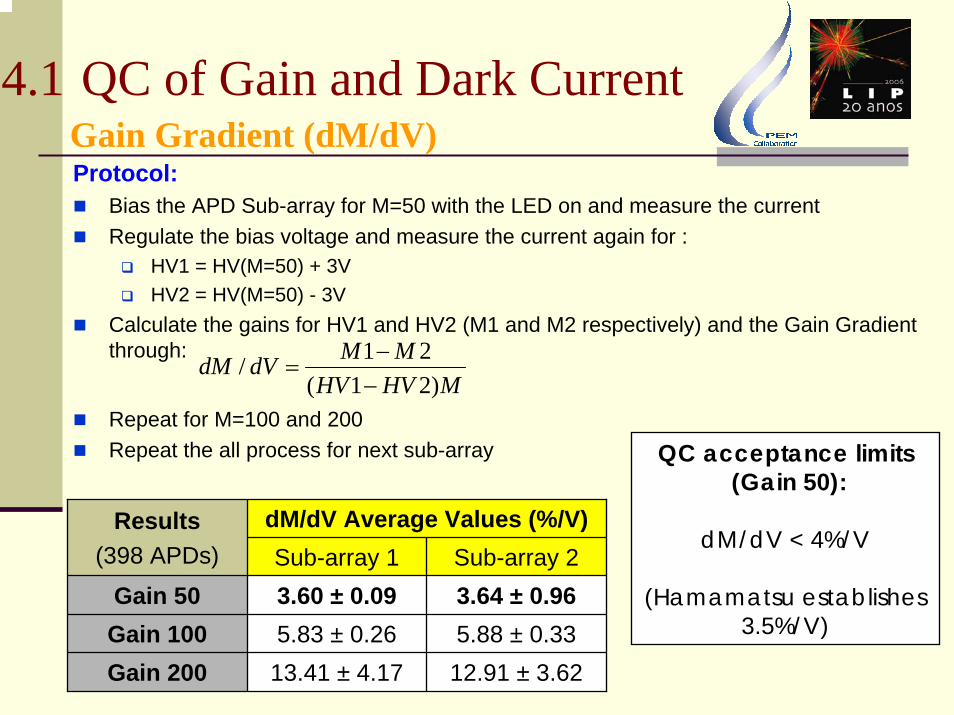
First Conclusion:From all 398 APDs, only 1 was rejected!
Didn’t pass the GAIN GRADIENT QC!
4.1 QC of Gain and Dark Current

Measurement parameters:Discrete amplification electronicsCesium radioactive source (137Cs, 662 keV, 93 µCi) 32 LYSO:Ce polished crystals matrix wrapped in TyvekAPDs polarized at gain 50Stable temperature
Data treatment done in order to obtain:- Relative Gain variation- Relative gain variation (within sub-array)
The following parameters were measured for 397* APDs:662 keV Peak Position per APD pixelPedestal positions per acquisition run
The same referenceAPD array was
measured everydayin order to controlsystematic errors!
FIT
4.2 QC of Relative Gain
*1APD failed previous QC

Shaper Module
HV SupplyN470
ADCV785
Dual TimerV993B
DC Supply
Electronics
Acquisition PC
VME/PCI Controler
32 LEMO Cables
GATE Signal
Peltier
Digital Multimeter
137Cs
GATE Signal
32 LYSO:Cepolished Crystals with
Tyvek Wrapping
LYSO:Ce Matrix(4x8)
Tyvek Reflector(250 µm) and
Optical Grease
APD Array
Setup4.2 QC of Relative Gain

0
200
400
600
800
1000
1200
1400
1600
1800
0.5 0.6 0.7 0.8 0.9 1.0 1.1 1.2 1.3 1.4 1.5Vn
Núm
ero
de P
íxei
s A
PD
Sub-array 1Sub-array 2Total
)()(
VaPixelperVppAverageVppPedestalPositionPeakFitVn −
=
PixelAPD
887,2 856,3 … 786,4857,2 894,7 … 864,3
… … … …824,3 875,1 … 797,8
H4
Average Peak position per pixel 853,1 885,4 … 799,8
60401
A1 B1 …1000110002
…
µ = 1.000σ = 0.064
Npixels =12 704 This normalization
removes dependency
on the electronic gain and crystal LY!
4.2 QC of Relative GainRelative Gain (Vn)
Vn
Num
bero
fAPD
Pix
els

0
500
1000
1500
2000
2500
3000
0.5 0.6 0.7 0.8 0.9 1.0 1.1 1.2 1.3 1.4 1.5Vn2
Núm
ero
de P
íxei
s A
PD
TotalSub-array1Sub-array2
)( 22 VaArrayperAverageVn
VnVn =
Array 2Pixel
APD 1,075 … 0,965 1,046 …0,934 … 1,003 0,963 …
… … … … …1,023 … 1,011 1,056 …
…
Array 1 Average Vn
Array11000110002
…60401
A1 H2 …
This normalization
further removes
dependency on sub-array
variation!
Accepted
4.2 QC of Relative GainRelative Gain within sub-array (Vn2)
µ = 1.000σ = 0.046
Npixels =12 704
QC acceptance interval (Gain 50):
0.8 < Vn2 < 1.3Vn2
Num
bero
fAPD
Pix
els

2. QC for Relative Gain
Second Conclusion:From all 397 APDs, only 1 was rejected!
1 APD pixel had relative gain (within array) below 0.8

Good Quality Control results (M=50):Average Bias Voltage = 410 VAverage Dark Current = 20.5 nAAverage dM/dV = 3.62 %/VRelative Gain within sub-array dispersion of 4.6 %
From the total of 398 APD Arrays, 396 APD arrays (99%) can be used in the final prototype
Due to this study, the S8550-01 APD Array is now being used by other Crystal Clear Collaboration groups
5. Conclusions