Embed Size (px)
Citation preview

HAL Id tel-01455081httpstelarchives-ouvertesfrtel-01455081
Submitted on 3 Feb 2017
HAL is a multi-disciplinary open accessarchive for the deposit and dissemination of sci-entific research documents whether they are pub-lished or not The documents may come fromteaching and research institutions in France orabroad or from public or private research centers
Lrsquoarchive ouverte pluridisciplinaire HAL estdestineacutee au deacutepocirct et agrave la diffusion de documentsscientifiques de niveau recherche publieacutes ou noneacutemanant des eacutetablissements drsquoenseignement et derecherche franccedilais ou eacutetrangers des laboratoirespublics ou priveacutes
Characterization and modeling of graphene-basedtransistors towards high frequency circuit applications
Jorge Daniel Aguirre Morales
To cite this versionJorge Daniel Aguirre Morales Characterization and modeling of graphene-based transistors to-wards high frequency circuit applications Other Universiteacute de Bordeaux 2016 English NNT 2016BORD0235 tel-01455081
THEgraveSE PREacuteSENTEacuteE
POUR OBTENIR LE GRADE DE
DOCTEUR DE
LrsquoUNIVERSITEacute DE BORDEAUX
EacuteCOLE DOCTORALE de Sciences Physiques et de lrsquoIngeacutenieur
SPEacuteCIALITEacute Eacutelectronique
Par Jorge Daniel AGUIRRE MORALES
Characterization and Modeling of Graphene-based Transistors
towards High Frequency Circuit Applications
Sous la direction de Thomas ZIMMER
(Co-encadrant Seacutebastien FREacuteGONEgraveSE)
Soutenue le 17 Novembre 2016
Membres du jury
Mme MANEUX Cristell Professeure Universiteacute de Bordeaux Preacutesidente
M LEMME Max Christian Professeur Universitaumlt Siegen Rapporteur
M GRASSER Tibor Professeur Universitaumlt Wien Rapporteur
M DERYCKE Vincent Chargeacute de Recherche HDR CEA Examinateur
M ZIMMER Thomas Professeur Universiteacute Bordeaux Directeur de thegravese
M FREacuteGONEgraveSE Seacutebastien Chargeacute de Recherche CNRS Talence Co-encadrant
For Amaury my sister and my parents
ldquoGraphene is the hero we deserve but not the one we can use right
now So we will research it Because its worth it Because it is not our hero
It is a silent guardian a watchful protector The dark slicerdquo
Acknowledgements
I would like to extend my sincere gratitude to all the reviewers for accepting to evaluate this
work to Mr Max C Lemme professor at the University of Siegen and Mr K Tibor Grasser
professor at the University of Vienna who very kindly agreed to be the scientific evaluators of this
thesis My earnest thanks are also due to the rest of the jury with Mr Vincent Derycke chargeacute de
recherche at LICSEN CEA and Mme Cristell Maneux professor with the University of Bordeaux
I have immense respect appreciation and gratitude towards my advisors Mr Thomas
ZIMMER professor at the University of Bordeaux and Mr Seacutebastien Freacutegonegravese chargeacute de
recherche CNRS for their consistent support and for sharing their invaluable knowledge experience
and advice which have been greatly beneficial to the successful completion of this thesis
Thanks to all Model team members for the occasional coffees and discussions especially
during our ldquoPhD Daysrdquo It was fun and rewarding to work alongside Franccedilois Marc Marina Deng
Mohammad Naouss Rosario DrsquoEsposito and Thomas Jacquet
I would also like to thank my friends Hajar Nassim Ashwin Ioannis and Andrii for their
support and all our happy get-togethers and for uplifting my spirits during the challenging times
faced during this thesis
I thank my IPN ldquoBaacutetizrdquo friends (Karina Jess Pintildea Osvaldo Pentildea Odette and Karen) and
my ldquoChapusrdquo friends (Daniela Samantha and Beto) for their priceless friendship and support during
the last 8 years I have been in France I would like to thank my family (uncles aunts cousins
grandparents) for their forever warm welcome every time I get the opportunity to go back to
Mexico
I am particularly grateful to my friends Chhandak Mukherjee and Kalparupa Mukherjee for
their precious support during this thesis for those dinners in which they made me discover the
delicious Indian food for all those trips to wonderful places and undoubtedly for their invaluable
friendship
A very special mention to Chhandak Mukherjee for his constant support his guidance and
for continually giving me the courage to make this thesis better
Last but definitely not the least I am forever indebted to my awesomely supportive parents
and my wonderful sister for inspiring and guiding me throughout the course of my life and hence
this thesis
Title Characterization and Modeling of Graphene-based Transistors towards High
Frequency Circuit Applications
Abstract
This work presents an evaluation of the performances of graphene-based Field-Effect
Transistors (GFETs) through electrical compact model simulation for high-frequency applications
Graphene-based transistors are one of the novel technologies and promising candidates for future
high performance applications in the beyond CMOS roadmap In that context this thesis presents a
comprehensive evaluation of graphene FETs at both device and circuit level through development of
accurate compact models for GFETs reliability analysis by studying critical degradation mechanisms
of GFETs and design of GFET-based circuit architectures
In this thesis an accurate physics-based large-signal compact model for dual-gate monolayer
graphene FET is presented This work also extends the model capabilities to RF simulation by
including an accurate description of the gate capacitances and the electro-magnetic environment The
accuracy of the developed compact model is assessed by comparison with a numerical model and
with measurements from different GFET technologies
In continuation an accurate large-signal model for dual-gate bilayer GFETs is presented As
a key modeling feature the opening and modulation of an energy bandgap through gate biasing is
included to the model The versatility and applicability of the monolayer and bilayer GFET compact
models are assessed by studying GFETs with structural alterations
The compact model capabilities are further extended by including aging laws describing the
charge trapping and the interface state generation responsible for bias-stress induced degradation
Lastly the developed large-signal compact model has been used along with EM simulations
at circuit level for further assessment of its capabilities in the prediction of the performances of three
circuit architectures a triple-mode amplifier an amplifier circuit and a balun circuit architecture
Keywords bilayer compact model graphene monolayer reliability Verilog-A
Titre Caracteacuterisation et Deacuteveloppement des Modegraveles Compacts pour des Transistors en
Graphegravene pour des Applications Haute Freacutequence
Reacutesumeacute
Ce travail preacutesente une eacutevaluation des performances des transistors agrave effet de champ agrave base
de graphegravene (GFET) gracircce agrave des simulations eacutelectriques des modegraveles compact deacutedieacutes agrave des
applications agrave haute freacutequence Les transistors agrave base de graphegravene sont parmi les nouvelles
technologies et sont des candidats prometteurs pour de futures applications agrave hautes performances
dans le cadre du plan drsquoaction laquo au-delagrave du transistor CMOS raquo Dans ce contexte cette thegravese preacutesente
une eacutevaluation complegravete des transistors agrave base de graphegravene tant au niveau du dispositif que du circuit
gracircce au deacuteveloppement de modegraveles compacts preacutecis pour des GFETs de lrsquoanalyse de la fiabiliteacute en
eacutetudiant les meacutecanismes critiques de deacutegradation des GFETs et de la conception des architectures
de circuits baseacutes sur des GFETs
Dans cette thegravese nous preacutesentons agrave lrsquoaide de certaines notions bien particuliegraveres de la
physique un modegravele compact grand signal des transistors FET agrave double grille agrave base de graphegravene
monocouche Ainsi en y incluant une description preacutecise des capaciteacutes de grille et de
lrsquoenvironnement eacutelectromagneacutetique (EM) ce travail eacutetend eacutegalement les aptitudes de ce modegravele agrave la
simulation RF Sa preacutecision est eacutevalueacutee en le comparant agrave la fois avec un modegravele numeacuterique et avec
des mesures de diffeacuterentes technologies GFET Par extension un modegravele grand signal pour les
transistors FET agrave double grille agrave base de graphegravene bicouche est preacutesenteacute Ce modegravele considegravere la
modeacutelisation de lrsquoouverture et de la modulation de la bande interdite (bandgap) dues agrave la polarisation
de la grille La polyvalence et lrsquoapplicabiliteacute de ces modegraveles compacts des GFETs monocouches et
bicouches ont eacuteteacute eacutevalueacutes en eacutetudiant les GFETs avec des alteacuterations structurelles
Les aptitudes du modegravele compact sont encore eacutetendues en incluant des lois de vieillissement
qui deacutecrivent le pieacutegeage de charges et la geacuteneacuteration drsquoeacutetats drsquointerface qui sont responsables de la
deacutegradation induite par les contraintes de polarisation Enfin pour eacutevaluer les aptitudes du modegravele
compact grand signal deacuteveloppeacute il a eacuteteacute impleacutementeacute au niveau de diffeacuterents circuits afin de preacutedire
les performances par simulations Les trois architectures de circuits utiliseacutees eacutetaient un amplificateur
triple mode un circuit amplificateur et une architecture de circuit laquo balun raquo
Mots-Cleacutes bicouche fiabiliteacute graphegravene modegravele compact monocouche Verilog-A
Uniteacute de recherche
Laboratoire de lrsquoInteacutegration du Mateacuteriau au Systegraveme (IMS) UMR 5218 351 Cours de la
Libeacuteration 33405 Talence Cedex France [Intituleacute ndeg de lrsquouniteacute et adresse de lrsquouniteacute de recherche]
Table of Contents
Introduction 19
A) Background 19
B) Carbon-based Devices for Nanoelectronics 21
C) Motivation of this thesis 22
D) Thesis Outline 23
Chapter 1 Monolayer GFET Compact Model 25
A) Physics of graphene 25
1 Energy Band Structure 25
2 Density of States and Carrier Sheet Densities 27
B) Physical Modeling of GFETs 28
1 The Quantum Capacitance 29
2 Differentiation of Carrier Transport Behavior 29
3 The Saturation Velocity 30
4 Small-Signal Parameters 31
C) The Electrical Compact Models 32
D) A Large-Signal Monolayer Graphene Field-Effect Transistor Compact Model
for RF-Circuit Applications (This Work) [88] [89] 37
1 The Carrier Densities 37
2 The Quantum Capacitance 38
3 The Channel Voltage 39
4 The Drain-to Source Current 42
5 The Residual Carrier Density 43
6 The Parasitic Series Resistances 44
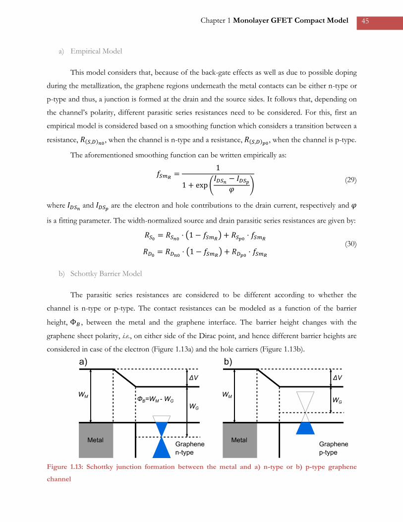
a) Empirical Model 45
b) Schottky Barrier Model 45
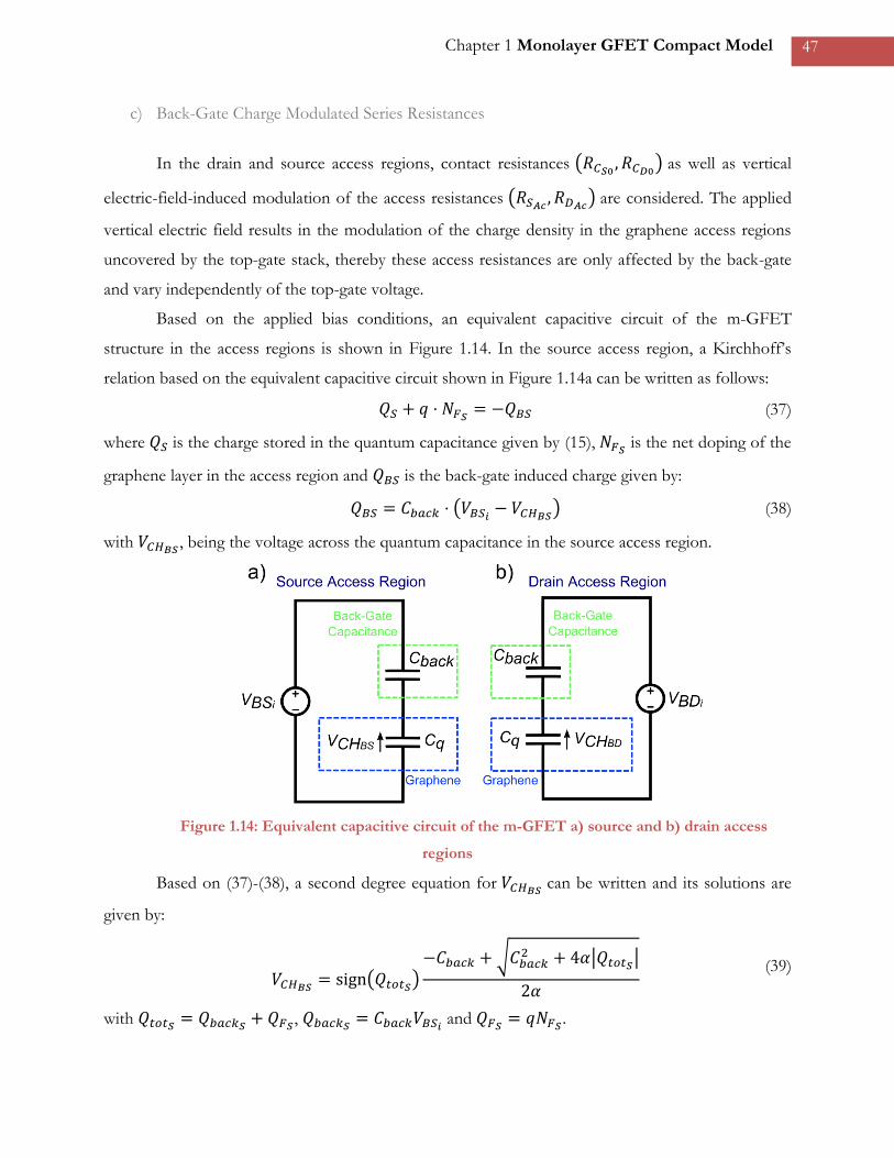
c) Back-Gate Charge Modulated Series Resistances 47
7 Gate resistance - Scalable Model 48
8 Gate Capacitances 49
9 Numerical Model [102] 50
10 Compact Model Implementation 51
a) The Drain-to-Source Current 51
b) Gate Capacitances 53
E) Results amp Discussion 55
1 Columbia Universityrsquos Device 55
2 University of Lillersquos CVD Device 60
a) Device Characterization 61
b) Electro-Magnetic Simulations 62
c) DC and S-Parameter Results 64
F) Application- DUT from University of New Mexico [103] 69
1 Device Description [103] 69
2 Device Modeling 70
G) Conclusion 74
Chapter 2 Bilayer GFET Compact Model 77
A) Opening an Energy Bandgap 77
1 Energy Band Structure of Bilayer graphene 79
2 Density of States of Bilayer Graphene 80
B) State of the Art 81
C) An Accurate Physics-Based Compact Model for Dual-Gate Bilayer Graphene
FETs (This Work) [127] [128] 81
1 The Energy Bandgap 82
2 The Carrier Densities 83
3 The Channel Voltage 84
4 The Shift in the Dirac Voltage 86
5 The Residual Carrier Density 87
6 The Parasitic Series Resistances 87
7 Compact Model Implementation 89
D) Results amp Discussion 91
E) Application- DUT from University of Siegen [129] 95
1 Device fabrication [129] 95
2 Modelling of DC Characteristics 96
F) Conclusion 100
Chapter 3 Reliability-Aware Circuit Design 101
A) State of the Art 101
B) Experimental Details of Aging Tests 102
C) Aging Compact Model (This Work) [83] 106
1 Trap Generation 106
2 Interface State Generation 108
D) Aging Compact Model Validation 109
1 Charge Trapping Model 109
2 Unified Model combining Charge Trapping and Interface State Generation 113
E) Conclusion 113
Chapter 4 Circuit Design 115
A) Triple Mode Amplifier 115
1 Mode 1 Common-Source Mode 116
2 Mode 2 Common-Drain Mode 117
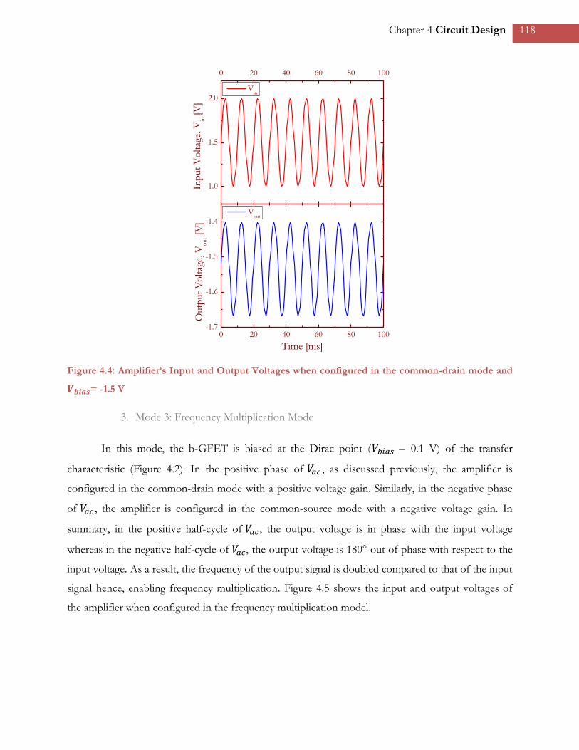
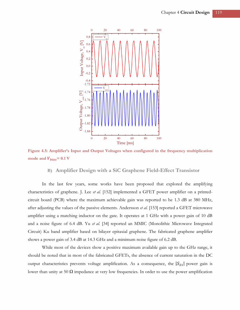
3 Mode 3 Frequency Multiplication Mode 118
B) Amplifier Design with a SiC Graphene Field-Effect Transistor 119
1 DC and S-Parameter characteristics of the SiC GFET 120
2 Amplifier Circuit Design 125
3 Results 127
C) Balun Circuit Architecture 129
D) Conclusion 131
Conclusions amp Perspectives 133
References 137
Appendix A 151
Appendix B 153
List of Publications 155
List of Figures
Figure 01 Trend in the International Technology Roadmap for Semiconductors ldquoMore Moorerdquo
stands for miniaturization of the digital functions ldquoMore than Moorerdquo stands for the functional
diversification and ldquoBeyond CMOSrdquo stands for future devices based on completely new functional
principles [7] 20
Figure 02 Carbon allotropes buckminsterfullerene carbon nanotubes (CNTs) and graphene [10] 21
Figure 11 a)Graphene honeycomb lattice structure and b) Brillouin zone[48] 26
Figure 12 Electronic band structure of graphene [48] 27
Figure 13 a) Density of States per unit cell as a function of energy for trsquo = 0 and b) Zoom in to the
Density of States close to the neutrality point [48] 28
Figure 14 Cross-sectional view of the m-GFET structure 28
Figure 15 Top-Gate Capacitance CG 29
Figure 16 Cross-sectional view of the m-GFET structure with definition of the parasitic series
resistances 30
Figure 17 Saturation velocity dependency on the carrier density [60] (modified) The red line
represents the saturation velocity for T = 80 K and the blue line for T = 300 K 31
Figure 18 Timeline of Compact Model Development 33
Figure 19 Quantum Capacitance Cq versus Channel Voltage VCH 39
Figure 110 Equivalent capacitive circuit of the m-GFET structure 39
Figure 111 GFET channel conditions a) n-type channel b) p-type channel c) n-type to p-type
channel and d) p-type to n-type channel CNP is the charge neutrality point 41
Figure 112 Spatial inhomogeneity of the electrostatic potential [96] 44
Figure 113 Schottky junction formation between the metal and a) n-type or b) p-type graphene
channel 45
Figure 114 Equivalent capacitive circuit of the m-GFET a) source and b) drain access regions 47
Figure 115 Intrinsic Large-Signal Equivalent Circuit 50
Figure 116 Numerical Model Block Diagram the model utilizes three main functions lsquofsolversquo to
solve non-linear system equations lsquotrapzrsquo to calculate numerical integrations and lsquodiffrsquo to perform
numerical differentiations 51
Figure 117 Comparison of the measured (symbols) a) transfer characteristic (IDS-VGS) and b)
transconductance (gm-VGS) with the numerical model (dashed lines) and the compact model results
(solid lines) for VBS = -40 V and VDS = -05 -10 and -15 V 56
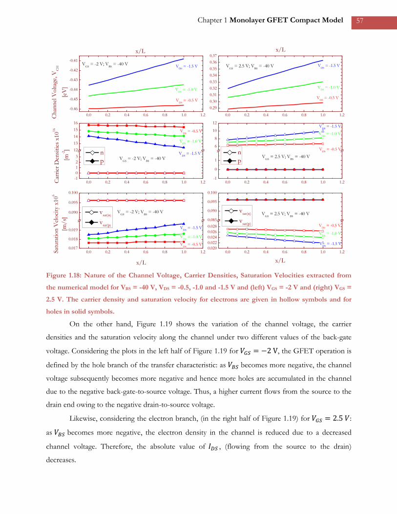
Figure 118 Nature of the Channel Voltage Carrier Densities Saturation Velocities extracted from
the numerical model for VBS = -40 V VDS = -05 -10 and -15 V and (left) VGS = -2 V and (right)
VGS = 25 V The carrier density and saturation velocity for electrons are given in hollow symbols
and for holes in solid symbols 57
Figure 119 Nature of the Channel Voltage Carrier Densities Saturation Velocities extracted from
the numerical model for VDS = -1 V VBS = -20 -40 and -60 V and (left) VGS = -2 V and (right) VGS =
25 V The carrier density and saturation velocity for electrons are given in hollow symbols and for
holes in solid symbols 58
Figure 120 Nature of the Channel Voltage Carrier Densities Saturation Velocities extracted from
the numerical model for VGS = VDirac VBS = -40 V and VDS = -05 -10 and -15 V The carrier density
and saturation velocity for electrons are given in hollow symbols and for holes in solid symbols 59
Figure 121 Comparison of the measured (symbols) a) output characteristic (IDS-VDS) and b) output
conductance (gds-VDS) with the numerical model (dashed lines) and the compact model results (solid
lines) for VBS = -40 V and VGS = 0 -15 -19 and -30 V 59
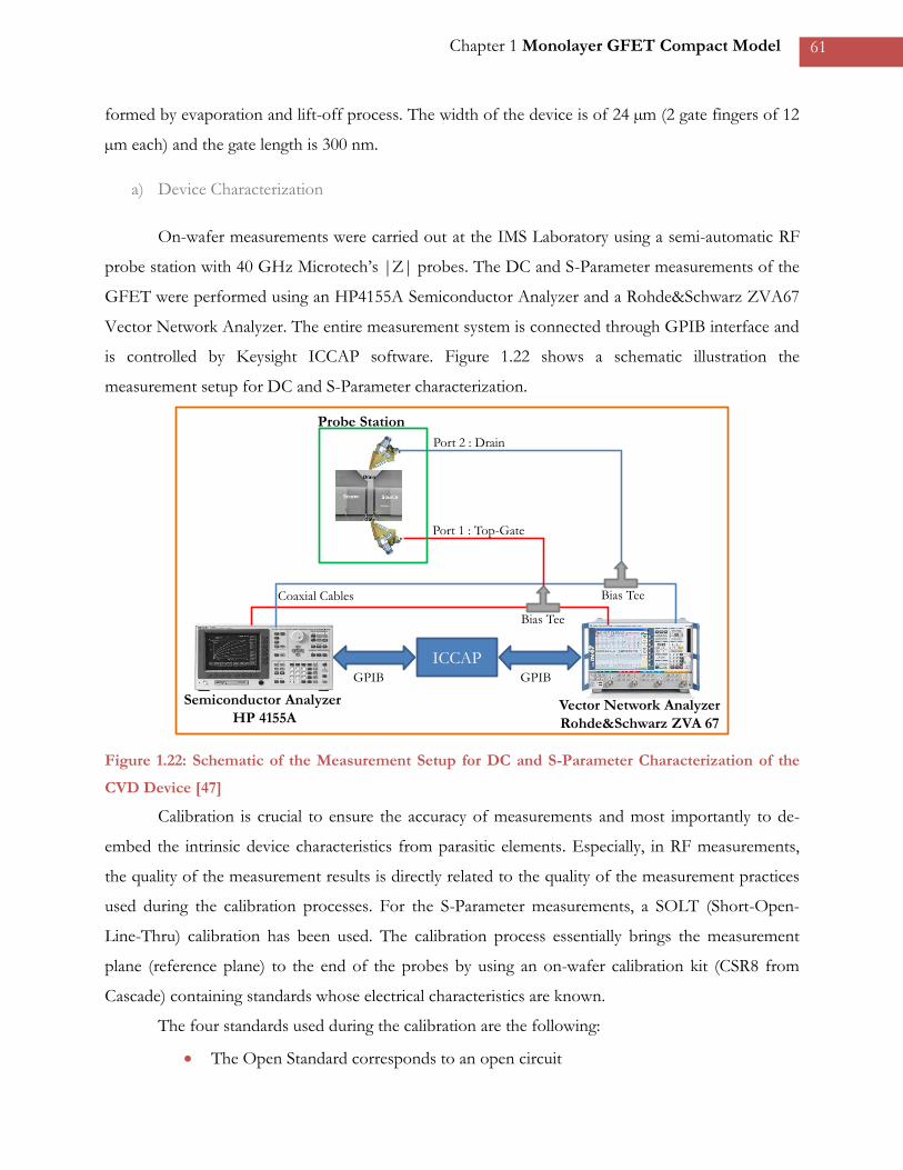
Figure 122 Schematic of the Measurement Setup for DC and S-Parameter Characterization of the
CVD Device [47] 61
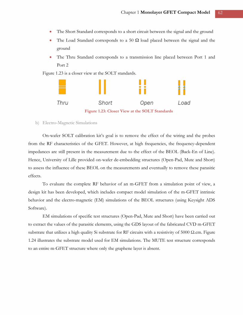
Figure 123 Closer View at the SOLT Standards 62
Figure 124 Substrate Model and Structure used for EM Simulation 63
Figure 125 a) Open-Pad b) Mute and c) Short EM test structures 63
Figure 126 Large-Signal equivalent circuit of the m-GFET in measurement conditions 64
Figure 127 Comparison of the measured (symbols) a) transfer characteristic (IDS-VGS) and b)
transconductance (gm-VGS) with the compact model (solid lines) for VDS varying from 025 V to 125
V in steps of 025 V 65
Figure 128 Comparison of the measured (symbols) output characteristics (IDS-VDS) with the
compact model (solid lines) for VGS varying from -1 V to 15 V in steps of 05 V 65
Figure 129 Comparison of the compact model presented in this work (solid lines) with the compact
model presented in previous works (dashed lines) [78] 66
Figure 130 Comparison of the S-Parameter measurements (symbols) with the compact model (solid
lines) for VGS = 250 mV and VDS = 500 mV and 15 V for a frequency range of 400 MHz to 40 GHz
66
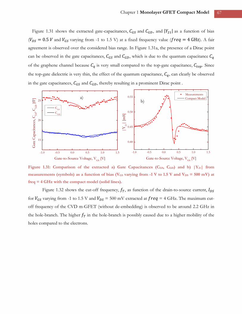
Figure 131 Comparison of the extracted a) Gate Capacitances (CGS CGD) and b) |Y21| from
measurements (symbols) as a function of bias (VGS varying from -1 V to 15 V and VDS = 500 mV) at
freq = 4 GHz with the compact model (solid lines) 67
Figure 132 Comparison of the extracted cut-off frequency fT from measurements (symbols) as a
function of the drain-to-source current at freq = 4 GHz with the compact model (solid lines) 68
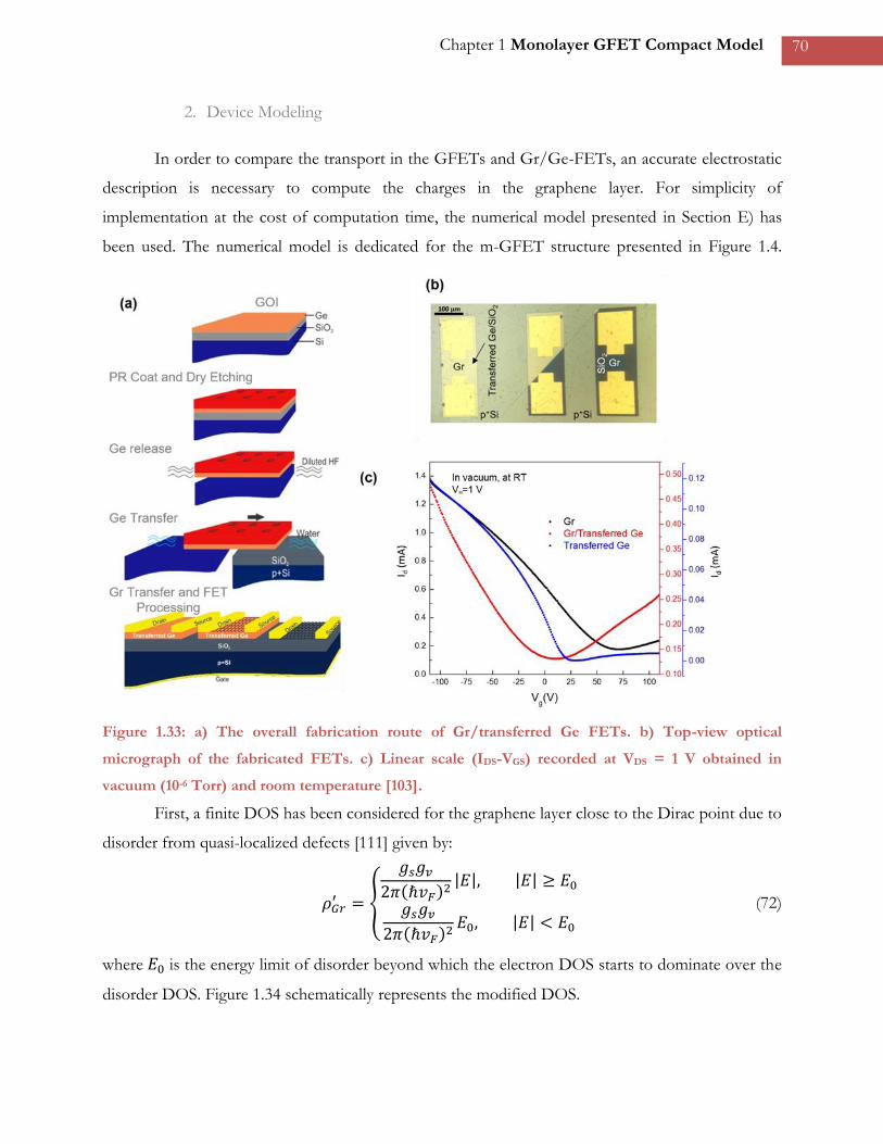
Figure 133 a) The overall fabrication route of Grtransferred Ge FETs b) Top-view optical
micrograph of the fabricated FETs c) Linear scale (IDS-VGS) recorded at VDS = 1 V obtained in
vacuum (10-6 Torr) and room temperature [103] 70
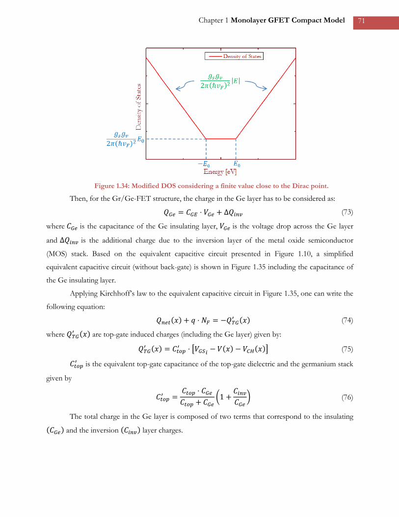
Figure 134 Modified DOS considering a finite value close to the Dirac point 71
Figure 135 Equivalent capacitive circuit for the GrGe-FET structure 72
Figure 136 Carrier density (electron and hole) in the Ge region of the Ge-FET 72
Figure 137 Channel Voltage in the graphene layer versus the Gate-to-Source Voltage The GrGe-
FET structure has been simulated with (green line) and without (blue line) considering the inversion
charge Cinv 73
Figure 138 Transfer Characteristics for the a) GFET and b) GrGe-FET for different VDS = 1 mV
10 mV 100 mV 05 V and 1 V Measurement (symbols) and model (solid lines) 73
Figure 21 Energy bandgap versus GNR width [115] 78
Figure 22 a) Schematic representation of the effect of uniaxial tensile stress on graphene Energy
band structure of a) unstrained graphene and b) 1 tensile strained graphene [116] 78
Figure 23 Schematic of the A2-B1 Bernal stacked bilayer lattice [124] 79
Figure 24 Energy band structure around the first Brillouin zone of large area-graphene GNR
unbiased and biased bilayer graphene [115] 80
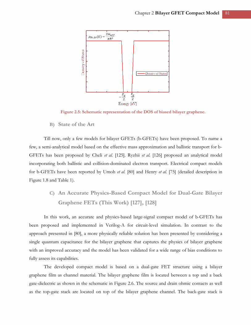
Figure 25 Schematic representation of the DOS of biased bilayer graphene 81
Figure 26 Cross sectional view of the b-GFET structure including parasitic access resistances 82
Figure 27 Electric-field dependence of tunable energy bandgap in graphene bilayer [120] 82
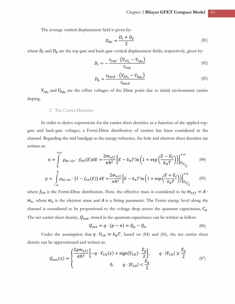
Figure 28 Illustration of the Net Carrier Sheet density as a function of the Channel Voltage for
different energy bandgap values 84
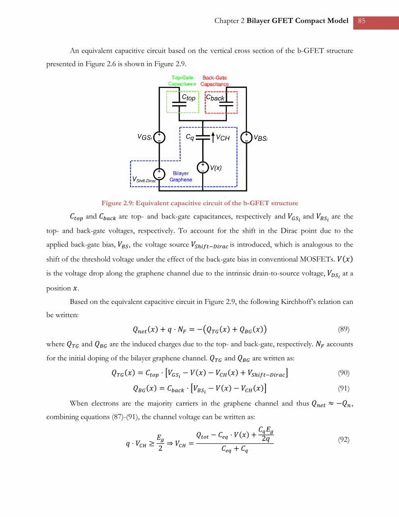
Figure 29 Equivalent capacitive circuit of the b-GFET structure 85
Figure 210 Equivalent capacitive circuit of the b-GFET access regions 88
Figure 211 Comparison of the measured (symbols) [117] a) transfer characteristics (IDS-VGS) and b)
transconductance (gm-VGS) with the compact model (solid lines) for VDS = -2 V and VBS varying from
0 V to -60 V 92
Figure 212 Comparison of the measured (symbols) [117] output characteristics (IDS-VDS) with the
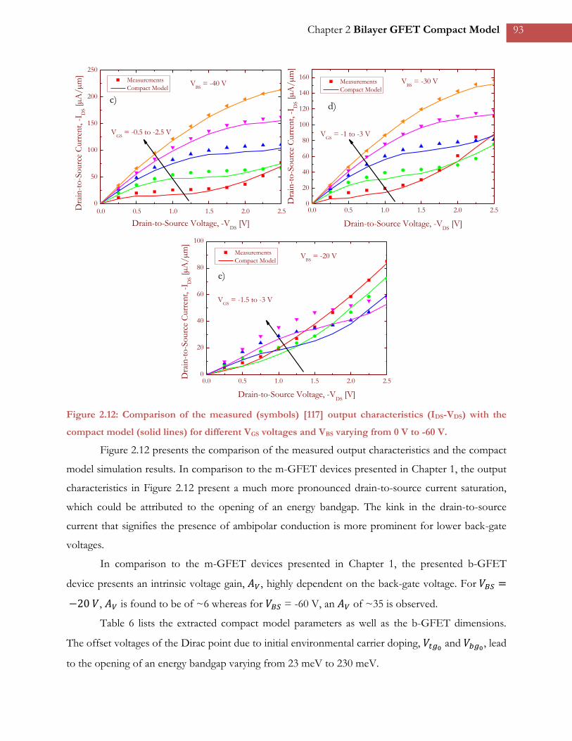
compact model (solid lines) for different VGS voltages and VBS varying from 0 V to -60 V 93
Figure 213 a) Cross sectional schematic of stacked bilayer graphene FET (BIGFET) and b) Optical
Micrograph showing a completed device after final lift-off step [129] 96
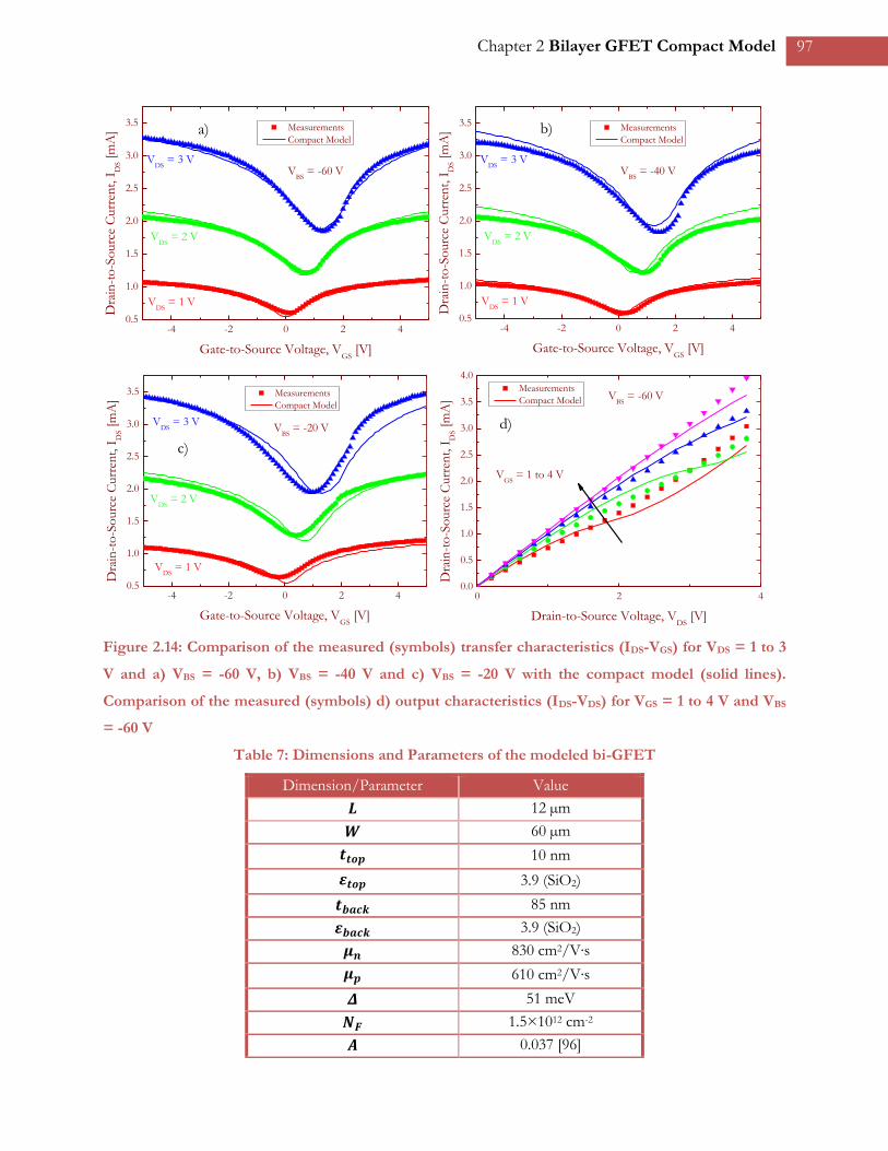
Figure 214 Comparison of the measured (symbols) transfer characteristics (IDS-VGS) for VDS = 1 to 3
V and a) VBS = -60 V b) VBS = -40 V and c) VBS = -20 V with the compact model (solid lines)
Comparison of the measured (symbols) d) output characteristics (IDS-VDS) for VGS = 1 to 4 V and VBS
= -60 V 97
Figure 215 TCAD Simulation results ndash Formation of a depletion capacitance in presence of external
back-gate voltages for different substrate doping densities 99
Figure 216 TCAD Simulation results ndash Formation of a depletion region up to a certain depth for
different back-gate voltages 99
Figure 31 Schematic of 120491119933119931 shift under positive bias stress [135] 103
Figure 32 Time evolution of 120491119933119931 at various positive stressing 119933119913119930 at 25 degC [135] 103
Figure 33 Transfer characteristics IDS-VBS curves shift under a constant voltage stress of 10 V [136]
104
Figure 34 Time dependence of 120491119933119931 under constant gate stress biases (VST) of 10 and -10 V [136] at
room temperature (RT) 104
Figure 35 Time dependence of 120491119933119931 under dynamic stresses with a duty cycle of 05 and a period of
2000 s [136] 105
Figure 36 Evolution of IDS-VGS as a function of stress time for CVD GFETs [146] [147] 106
Figure 37 Electron and hole trapping in the graphene channel in response to a top-gate stress
voltage 106
Figure 38 Electron and hole trapping in the graphene channel in response to back-gate stress
voltage 107
Figure 39 Comparison of the GFET back-gate transfer measurements [136]characteristics with the
aging compact model 110
Figure 310 Evolution of 120491119933119931 as a function of stress time for GFETs at different polarities of stress
voltages [136] 111
Figure 311 Evolution of 120491119933119931 [136] under dynamic stresses with a duty cycle of 05 and a period of
2000 s 111
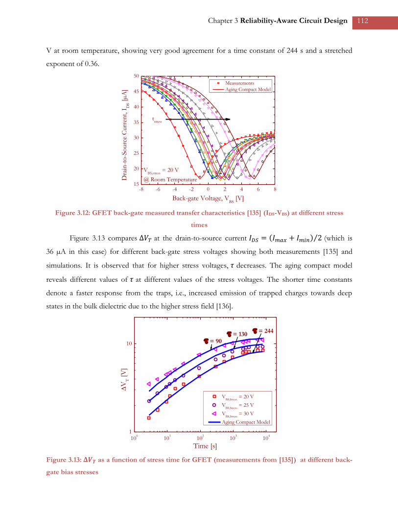
Figure 312 GFET back-gate measured transfer characteristics [135] (IDS-VBS) at different stress
times 112
Figure 313 120491119933119931 as a function of stress time for GFET (measurements from [135]) at different
back-gate bias stresses 112
Figure 314 Measurement of CVD GFET and comparison with the a) aging compact model
including charge trapping and b) unified model including charge trapping and interface state
generation [146] [147] 113
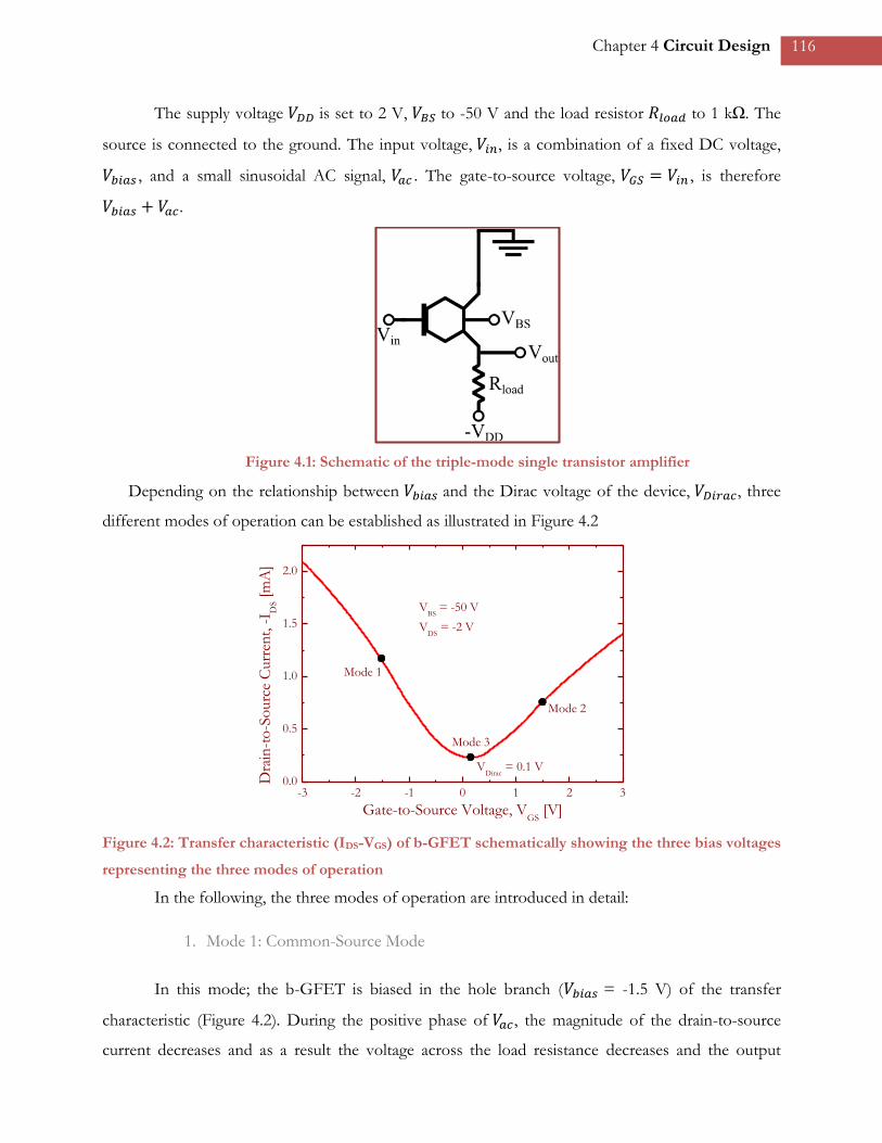
Figure 41 Schematic of the triple-mode single transistor amplifier 116
Figure 42 Transfer characteristic (IDS-VGS) of b-GFET schematically showing the three bias voltages
representing the three modes of operation 116
Figure 43 Amplifierrsquos Input and Output Voltages when configured in the common-source mode
and 119933119939119946119938119956= -15 V 117
Figure 44 Amplifierrsquos Input and Output Voltages when configured in the common-drain mode and
119933119939119946119938119956= -15 V 118
Figure 45 Amplifierrsquos Input and Output Voltages when configured in the frequency multiplication
mode and 119933119939119946119938119956= 01 V 119
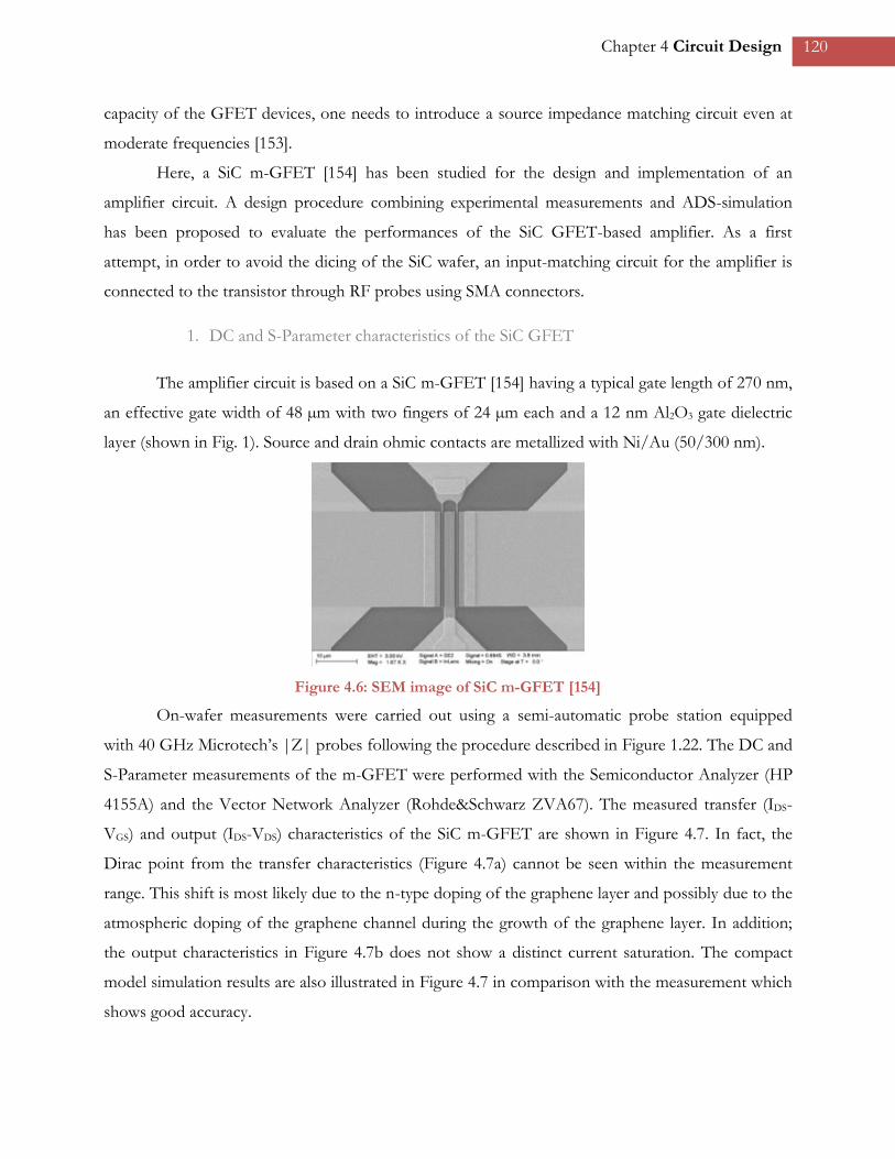
Figure 46 SEM image of SiC m-GFET [154] 120
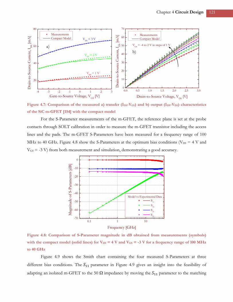
Figure 47 Comparison of the measured a) transfer (IDS-VGS) and b) output (IDS-VDS) characteristics
of the SiC m-GFET [154] with the compact model 121
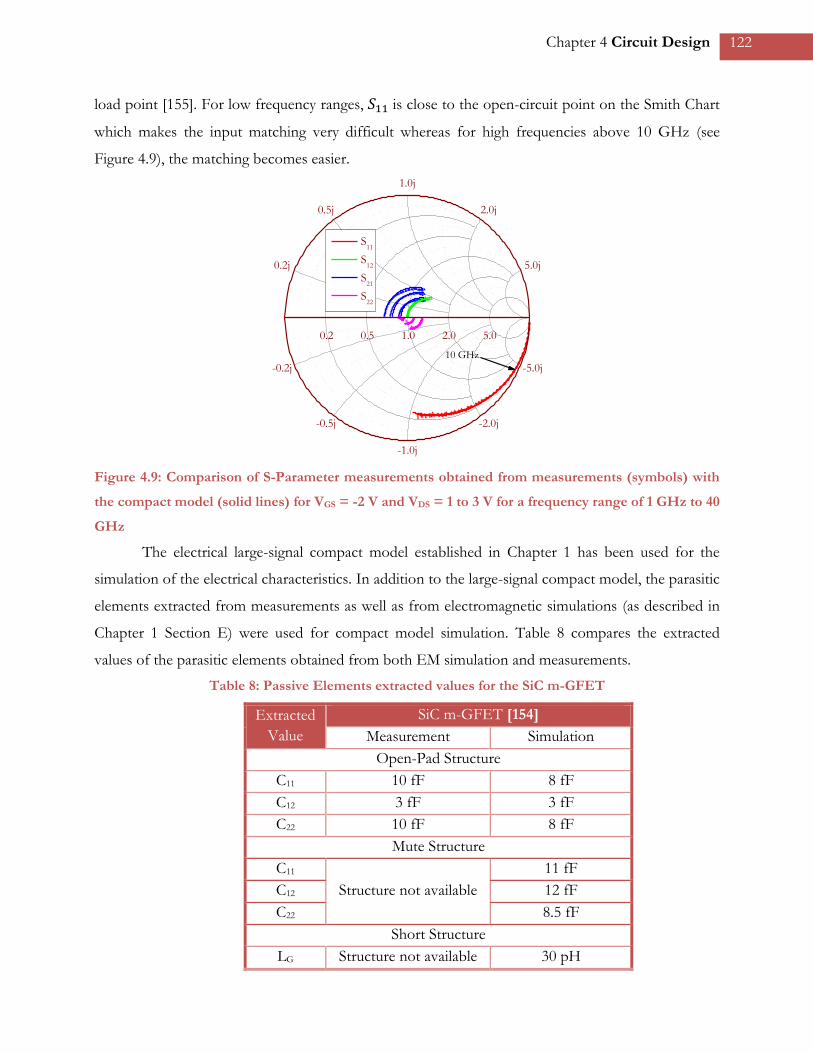
Figure 48 Comparison of S-Parameter magnitude in dB obtained from measurements (symbols)
with the compact model (solid lines) for VDS = 4 V and VGS = -3 V for a frequency range of 100
MHz to 40 GHz 121
Figure 49 Comparison of S-Parameter measurements obtained from measurements (symbols) with
the compact model (solid lines) for VGS = -2 V and VDS = 1 to 3 V for a frequency range of 1 GHz
to 40 GHz 122
Figure 410 Comparison of the extracted gate capacitances CGS and CGD from measurements and
from compact model simulation as a function of VGS for VDS = 1 to 3 V 124
Figure 411 Comparison of the extracted a) Current Gain (|H21|) and b) Unilateral Power Gain (U)
extracted from measurements and from compact model simulation as a function of frequency for
VGS = -2 V and VDS = 1 to 3 V 124
Figure 412 |Z| RF Probe measurement bench 125
Figure 413 ADS-Simulation model of the Probe-Thru-Probe system 125
Figure 414 Comparison of the probe head S-Parameter measurements with the developed model on
a 114 ps thru standard 126
Figure 415 (Left) Fabricated PCB Input-matching circuit and (Right) Developed model of the PCB
circuit 126
Figure 416 Comparison of the LC input-matching circuit measurements (symbols) with the
developed model (solid lines) 127
Figure 417 ADS Simulation SiC GFET Amplifier Circuit 127
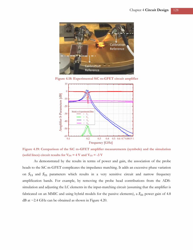
Figure 418 Experimental SiC m-GFET circuit amplifier 128
Figure 419 Comparison of the SiC m-GFET amplifier measurements (symbols) and the simulation
(solid lines) circuit results for VDS = 4 V and VGS = -3 V 128
Figure 420 S-Parameter of the SiC m-GFET amplifier obtained from ADS-simulation of the
assembly of the input-matching circuit and the SiC m-GFET 129
Figure 421 Schematic circuit diagram of the SiC m-GFET balun architecture 130
Figure 422 EM structure used for post-layout simulation of the GFET balun architecture 130
Figure 423 Phase Shift between Port 2 and Port 3 (in green simulation with BEOL and in red
without BEOL) 131
Figure 424 Balunrsquos Output Voltages VDS1 and VDS2 for and input voltage of 02 V at 1 MHz 131
19 Introduction
INTRODUCTION
he discovery of the appealing electronic and physical properties of graphene was
first achieved by isolating single layers of graphene from graphite in the last decade
[1] Since then Graphene Field-Effect Transistors (GFETs) have been studied
extensively as a central element to complement and extend silicon-based electronics for future high-
performance circuit applications Among the several carbon allotropes graphene appears to be
advantageous for high-speed electronics because of its 2-D structure that can provide very high
carrier mobilities Besides a major advantage of graphene lies in its compatibility for integration into
the existing process fabrication flow of silicon-based technologies Despite being in an early stage of
development several recent works targeting high-frequency applications using graphene-based
devices have been proposed With a similar motivation this thesis presents a comprehensive study of
GFET devices in order to realize accurate electrical compact model solutions for future high-speed
circuit design
A) Background
Ever since the first functional Field-Effect Transistor (FET) was reported in 1952 [2] the
improvement of the performances by making the electronic components smaller faster and cheaper
has been a constant motivation for the electronics industry over several decades In his attempt to
predict the future Gordon Moore proposed in 1965 what was later called the Moorersquos law [3] where
he predicted that the number of transistors in an integrated circuit doubles approximately every two
years Since then all the semiconductor industries have diligently followed this law in their
manufacturing process However in the last few years Moorersquos law has started to seem unattainable
as the size of the silicon transistors has been shrunk down to the atomic scale With the drastic
T
20 Introduction
scaling down of transistors the normal laws of physics would be impacted by quantum effects and
new technological challenges [4] arise as a consequence which sets a limit to further development
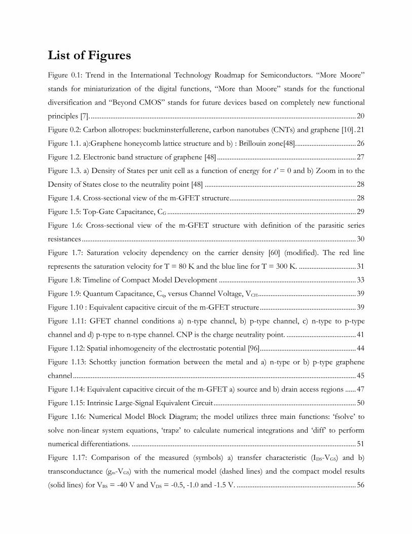
Therefore a strategy to overcome these limitations has been introduced and is known as ldquoMore
Moorerdquo (Figure 01) This strategy focuses on enhancing the performances of the devices further by
introducing new technology processes without altering its functional principle such as by introducing
strained silicon [5] or high-K gate insulators [6] In addition a second trend named ldquoMore-than-
Moorerdquo (Figure 01) has been introduced and it is characterized by the diversification of the
semiconductor-based devices This means that digital and non-digital functionalities such as analog
signal processing sensors actuators biochips etc are integrated into compact systems in order to
extend the range of applications fields
Figure 01 Trend in the International Technology Roadmap for Semiconductors ldquoMore Moorerdquo
stands for miniaturization of the digital functions ldquoMore than Moorerdquo stands for the functional
diversification and ldquoBeyond CMOSrdquo stands for future devices based on completely new functional
principles [7]
A third strategy known as ldquoBeyond CMOSrdquo (Figure 01) has also been introduced that
suggests the replacement of CMOS technology Therefore the scientific community has been
intensively searching for alternate means in order to propose new materials and device architectures
Consequently since the first report of the isolation of single atom thick graphene layers by
21 Introduction
Novoselov et al [1] graphene has become the center of attention in beyond CMOS community due
to its very promising properties such as high carrier mobilities thus making graphene seem suitable
for RF (Radio-Frequency) applications
B) Carbon-based Devices for Nanoelectronics
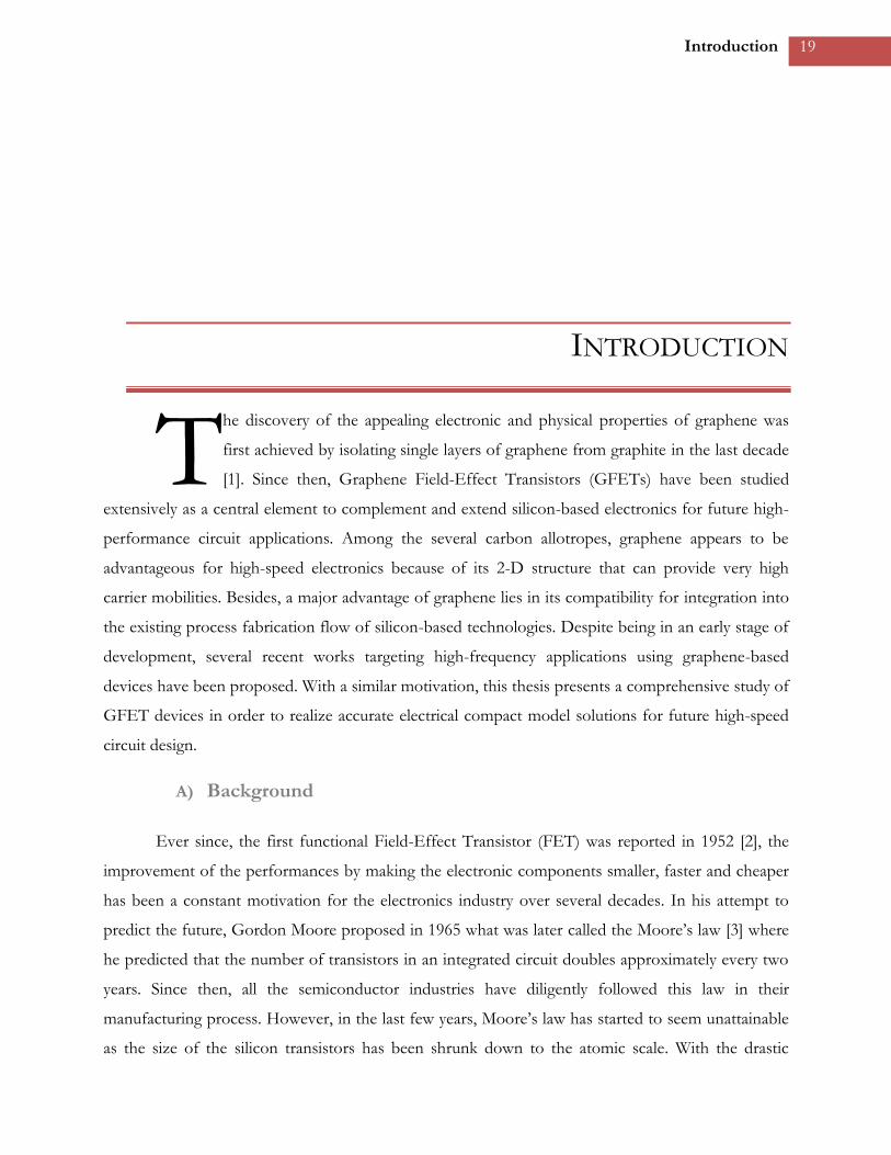
In the last few decades the family of known carbon allotropes has been significantly
extended In addition to the well-known carbon allotropes (coal diamond and graphite) new
allotropes (Figure 02) have been investigated for electronics such as buckminsterfullerene [8] (1985)
carbon nanotubes (CNT) [9] (1991) and graphene [1] (2004)
Figure 02 Carbon allotropes buckminsterfullerene carbon nanotubes (CNTs) and graphene [10]
Although buckminsterfullerene has been considered for FET fabrication [11] still little is
known about the actual properties of buckminsterfullerene-based FET On the other hand physics
of CNTs are quite extensively studied and the CNTs can be categorized into two groups single
walled CNTs and multi-walled CNTs Several works have demonstrated the potential of CNT for
22 Introduction
future generation integrated circuits such as high current densities [12] high thermal conductivity
[13] and tensile mechanical strength [14] Therefore numerous works exploiting the advantageous
properties of CNT for FET fabrication have been proposed [15] [16]
Graphene although first believed to be chemically unstable was finally synthetized in 2004
[1] and since then it has been focus of enthusiasm of several groups in the research community In
addition the first Graphene FET (GFET) device was reported in 2007 by Lemme et al [17]
Graphene a 2-D material that can deliver very high carrier mobilities has specific advantages
in its integration to the current fabrication process flow Several graphene FET fabrication processes
have been proposed so far such as mechanical exfoliation [18] liquid phase and thermal exfoliation
[19] [20] chemical vapor deposition (CVD) [21] and synthesis on SiC [22] Among these techniques
chemical vapor deposition appears to be a more viable solution towards graphene-based electronic
applications
One of the most remarkable properties of graphene for electronics is its very high carrier
mobility at room temperature [23] In the absence of ripples and charged impurities a carrier
mobility in excess of 2times106 cm2V∙s has been reported [24] [25] In perspective carrier mobilities of
1400 cm2V∙s and 8500 cm2V∙s have been obtained for conventional silicon CMOS [26] and
gallium arsenide [27] respectively On the downside large-area graphene is a gapless material
therefore the applicability of large-area graphene to digital applications is severely compromised and
thus it is not suitable for logic applications
Therefore in the last few years enormous efforts have been carried out in order to inspect
the properties of graphene in high frequency applications To this end GFETs with intrinsic cut-off
frequencies as high as 350 GHz [28]and 300 GHz [29] have been reported However due to the
absence of current saturation and high access resistances the extrinsic cut-off frequencies 119891119879 and
maximum oscillation frequency 119891119898119886119909 are below 50 GHz In comparison to other technologies cut-
off frequencies of 485 GHz for 29 nm silicon MOSFET [30] of 660 GHz for 20 nm mHEMT [31]
and of 100 GHz for 240 nm CNT FET [32] have been obtained which highlights that graphene has
still to reach the pinnacle of its performance
C) Motivation of this thesis
High-frequency applications based on graphene FETs have been emerging in the last few
years [33]ndash[45] With that in mind the objective of this thesis is to provide accurate solutions for
GFET modeling in DC and RF operation regimes In addition time-to-market and fabrication costs
23 Introduction
being two critical aspects this thesis covers some of the immediate reliability concerns to assess the
maturity of the technology and provides accurate modeling of failure mechanisms responsible for
transistor degradation over the circuit lifetime Finally as a first step towards high-frequency circuits
based on GFETs different circuit architectures based on GFETs are proposed and studied through
simulation in order to predict the circuit performances
D) Thesis Outline
This thesis is organized into four chapters
Chapter 1 presents a compact model for monolayer GFETs The chapter starts by a brief
introduction to the physics of monolayer graphene including its energy band structure and its density
of states Then the chapter presents the state of the art of the compact model evolution Later a
detailed description of the developed compact model suitable for DC and RF simulation is
presented Since the devices considered in this work have gate lengths higher than 100 nm the
presented compact model is based on the classical drift-diffusion transport approach Next the
compact model has been validated through comparison with DC and RF measurements from two
different technologies (exfoliated and CVD-grown graphene) Moreover electro-magnetic
simulations (EM) have been carried out in order to extract the values of parasitic elements due to the
BEOL (Back-End of Line) Finally the validity and potential of the model have been corroborated
by measurements on a different GFET technology with different structure procured through
collaboration with the University of New Mexico
Chapter 2 presents a compact model for bilayer GFETs Similarly to Chapter 1 the chapter
starts by a brief introduction to the physics of Bernal stacked bilayer graphene A state of the art of
models for bilayer GFETs is then provided Next the different attributes of the model are described
in detail The model has been validated through comparison with measurements from literature
Finally the potential of the proposed model has been further studied by validation through
comparison with artificially stacked bilayer graphene devices procured through collaboration with the
University of Siegen
Chapter 3 addresses the extension of the compact model presented in Chapter 1 to account
for critical degradation issues of graphene FET devices This part of the work has been carried out in
collaboration with Chhandak Mukherjee a post-doctoral researcher at IMS laboratory The chapter
starts by a state of the art of reliability studies on graphene FETs Next aging studies are performed
via stress measurements and aging laws have been implemented in the compact model Finally the
24 Introduction
accuracy of the aging compact model is validated through comparison with reported bias-stress
measurement results as well as aging measurements carried out at IMS Laboratory
Chapter 4 presents three different circuit architectures based on GFET devices in order to
explore the circuit level simulation capabilities of the compact models presented in Chapter 1 and
Chapter 2 First a triple mode amplifier based on bilayer graphene FET is presented and studied
through simulation Next the performances of an amplifier using a SiC GFET are evaluated through
comparison of measurement results with simulation results Finally a balun architecture based on
SiC GFETs is presented and its performances have been evaluated through EM-SPICE co-
simulations
Finally the conclusion provides an overview of this work and perspectives for further works
25 Chapter 1 Monolayer GFET Compact Model
Chapter 1
MONOLAYER GFET COMPACT MODEL
raphene the first of the so-called 2-D materials continues to grow as a central
material for future high-performance graphene Field-Effect Transistors (GFET)
circuit applications owing to its appealing electronic properties Thereby development of models
providing an insight into the carrier transport in GFET devices is highly desirable This chapter
provides a brief introduction to the physics of monolayer graphene followed by a description of the
primary aspects relevant for modeling of Monolayer GFETs (m-GFETs) towards circuit design
applications Then an overview of the state of the art of existing compact models for Monolayer
GFETs is presented Next the developed compact model and its different modules are presented
Thereafter the accuracy of the model has been validated through comparison with measurements of
two different GFET technologies that include exfoliated graphene FETs reported by [46] and CVD-
grown graphene FETs acquired in collaboration with the University of Lille [47] Finally the
potentials of the m-GFET model have been evaluated through measurement on a novel GFET
technology procured in collaboration with the University of New Mexico
A) Physics of graphene
1 Energy Band Structure
Carbon is the 15th most abundant element on Earth and many different carbon based
structures can be found in nature or be synthetized due to the flexibility of its bonding Graphene is
G
26 Chapter 1 Monolayer GFET Compact Model
a one atom thick 2-D carbon allotrope and has a hexagonal structure of sp2-bonded atoms as shown
in Figure 11a
Figure 11 a)Graphene honeycomb lattice structure and b) Brillouin zone[48]
In Figure 11 a1 and a2 are the lattice unit vectors and δ1 δ2 and δ3 are the nearest neighbor
vectors The two points K and Krsquo in Figure 11b are called the Dirac points The lattice vectors can
be written as [48]
119938120783 =119886
2(3 radic3) 119938120784 =
119886
2(3 minusradic3) (1)
with 119886 asymp 142 Å being the carbon-carbon distance
Graphene possesses an unusual energy band structure relative to conventional
semiconductors Considering a tight binding Hamiltonian for electrons in graphene and assuming
that electrons can hop to both the nearest- and the next-nearest-neighbor atoms the energy bands
can be derived as the following relations [48]
119864plusmn(119948) = plusmn119905radic3 + 119891(119948) minus 119905prime119891(119948) (2)
119891(119948) = 2 sdot 119888119900119904(radic3119896119910119886) + 4 sdot 119888119900119904 (radic3
2119896119910119886) 119888119900119904 (
3
2119896119909119886) (3)
where 119905 = 28 119890119881 is the nearest neighbor hopping energy 119905prime is the is the next nearest-neighbor
hopping energy and 119948 is the wave vector Figure 12 shows the resultant electronic band structure
27 Chapter 1 Monolayer GFET Compact Model
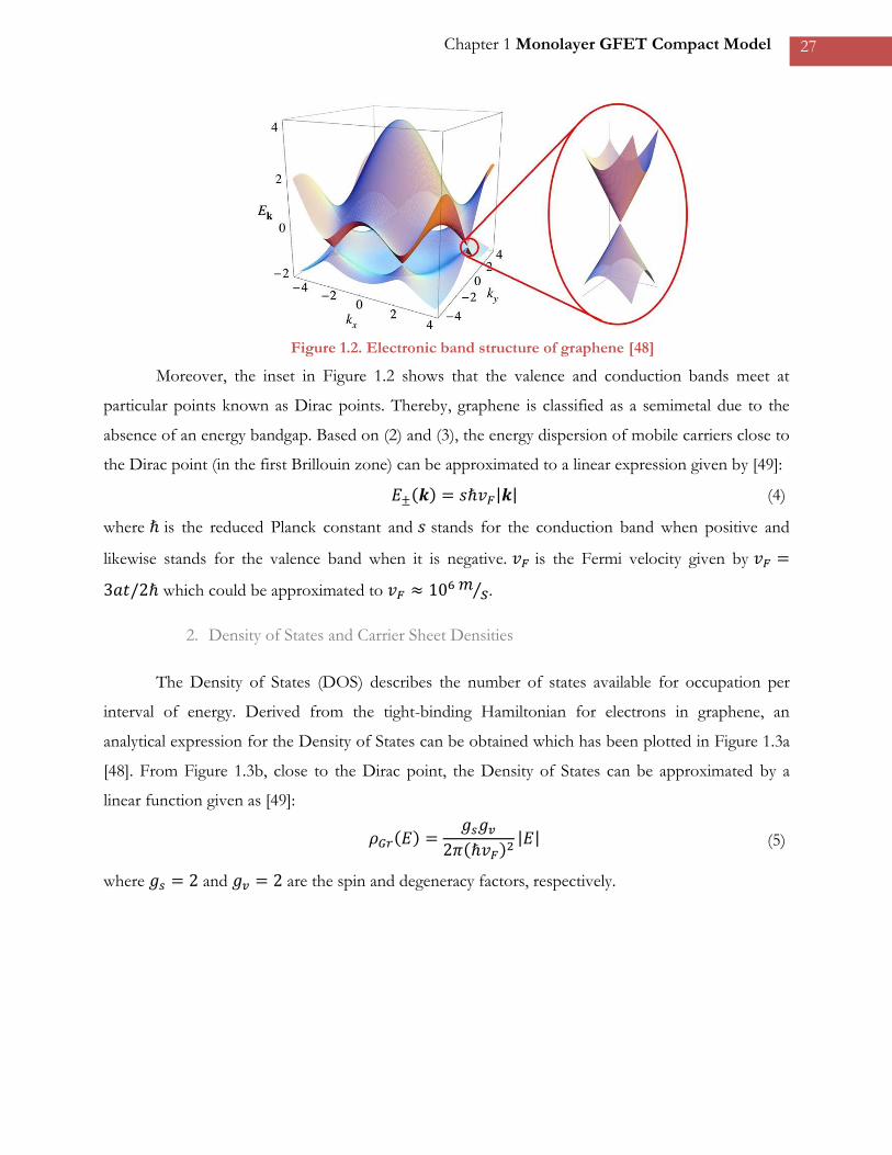
Figure 12 Electronic band structure of graphene [48]
Moreover the inset in Figure 12 shows that the valence and conduction bands meet at
particular points known as Dirac points Thereby graphene is classified as a semimetal due to the
absence of an energy bandgap Based on (2) and (3) the energy dispersion of mobile carriers close to
the Dirac point (in the first Brillouin zone) can be approximated to a linear expression given by [49]
119864plusmn(119948) = 119904ℏ119907119865|119948| (4)
where ℏ is the reduced Planck constant and 119904 stands for the conduction band when positive and
likewise stands for the valence band when it is negative 119907119865 is the Fermi velocity given by 119907119865 =
31198861199052ℏ which could be approximated to 119907119865 asymp 106119898
119904frasl
2 Density of States and Carrier Sheet Densities
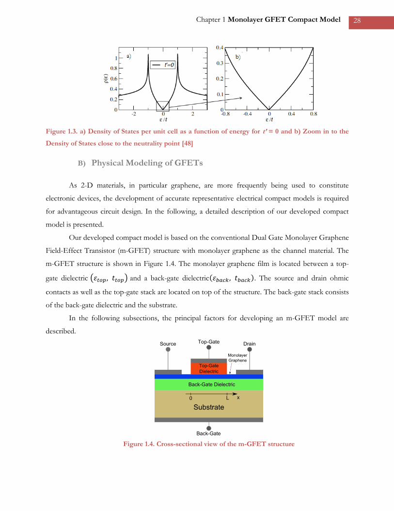
The Density of States (DOS) describes the number of states available for occupation per
interval of energy Derived from the tight-binding Hamiltonian for electrons in graphene an
analytical expression for the Density of States can be obtained which has been plotted in Figure 13a
[48] From Figure 13b close to the Dirac point the Density of States can be approximated by a
linear function given as [49]
120588119866119903(119864) =119892119904119892119907
2120587(ℏ119907119865)2|119864| (5)
where 119892119904 = 2 and 119892119907 = 2 are the spin and degeneracy factors respectively
28 Chapter 1 Monolayer GFET Compact Model
Figure 13 a) Density of States per unit cell as a function of energy for trsquo = 0 and b) Zoom in to the
Density of States close to the neutrality point [48]
B) Physical Modeling of GFETs
As 2-D materials in particular graphene are more frequently being used to constitute
electronic devices the development of accurate representative electrical compact models is required
for advantageous circuit design In the following a detailed description of our developed compact
model is presented
Our developed compact model is based on the conventional Dual Gate Monolayer Graphene
Field-Effect Transistor (m-GFET) structure with monolayer graphene as the channel material The
m-GFET structure is shown in Figure 14 The monolayer graphene film is located between a top-
gate dielectric (휀119905119900119901 119905119905119900119901) and a back-gate dielectric(휀119887119886119888119896 119905119887119886119888119896) The source and drain ohmic
contacts as well as the top-gate stack are located on top of the structure The back-gate stack consists
of the back-gate dielectric and the substrate
In the following subsections the principal factors for developing an m-GFET model are
described
Figure 14 Cross-sectional view of the m-GFET structure
29 Chapter 1 Monolayer GFET Compact Model
1 The Quantum Capacitance
The quantum capacitance first introduced by Serge Luryi in 1988 [50] is an important
modeling parameter to consider especially in a two plate capacitor with one of the plates having a
finite Density of States such as in graphene [51] Hence to properly describe the top-gate
capacitance 119862119866 one needs to account for this finite Density of States of graphene by considering a
quantum capacitance 119862119902 in series with the electrostatic top-gate capacitance 119862119905119900119901 (=0 119905119900119901
119905119905119900119901) as
shown in Figure 15 Here 휀119905119900119901 and 119905119905119900119901 are the dielectric constant and the thickness of the top-gate
dielectric Importantly in some cases especially for ultrathin high-K dielectrics the quantum
capacitance becomes dominant over the electrostatic top-gate capacitance rendering its modeling
essential
Figure 15 Top-Gate Capacitance CG
For graphene considering that the carrier distributions in the channel follow a Fermi-Dirac
distribution the quantum capacitance 119862119902 is given by [49]
119862119902 = 21199022119896119861119879
120587(ℏ119907119865)2ln 2 [1 + cosh (
119902119881119862119867119896119861119879
)] (6)
where 119902 is the electronic charge 119896119861 is the Boltzmann constant 119879 is the room temperature and 119881119862119867
is the channel voltage
2 Differentiation of Carrier Transport Behavior
Much of the interest in graphene as a channel material resides in its very high intrinsic carrier
mobilities which could be as high as 2times106 cm2 V-1 s-1 for suspended graphene [25] as well as because
of the possibility of modulating the carrier density as a function of an electric field [17] However
during the fabrication of the gate dielectric defects in the graphene lattice at the gate-
dielectricgraphene interface are formed which considerably decrease the intrinsic carrier mobility
due to scattering [52]
30 Chapter 1 Monolayer GFET Compact Model
In addition different carrier mobilities for holes and electrons arising from slightly different
effective masses may cause an asymmetry in the transport behavior of electrons and holes often
discerned in the transfer characteristics of the m-GFETs Moreover holes and electrons present
different cross-sections for impurity scattering [53] [54] which can make the asymmetry further
prominent Moreover due to the effect of the substrate the carrier mobility differs for electrons and
holes [55]
Furthermore the parasitic series resistance (Figure 16) which includes both the contact
resistance 119877119862 and the access resistance 119877119860119888119888119890119904119904 is an important factor contributing to this
asymmetry since depending on the polarity of the channel carrier the charge transfer between the
graphene sheet and the metal contacts leads to the creation of either a p-p or p-n junction enhancing
the asymmetry in the m-GFET transfer characteristics [56]
Hence an accurate description of the different electron and hole transport behavior in the
graphene channel is required
Figure 16 Cross-sectional view of the m-GFET structure with definition of the parasitic series
resistances
3 The Saturation Velocity
Under an applied external electric field induced by the applied bias conditions the carriers in
the graphene channel move with a drift velocity written as
119907119889119903119894119891119905 = 120583119864 (7)
where 120583 is the carrier mobility and 119864 the applied electric field However Monte Carlo simulations
[57]ndash[59] have shown that when the electric-field is increased (7) is no longer valid and the drift
velocity shows a soft-saturation (Figure 17) [60] which for a fixed value of temperature could be
approximated by the following expression [61]
31 Chapter 1 Monolayer GFET Compact Model
119907119889119903119894119891119905 =
120583119864
[1 + (120583|119864|119907119904119886119905
)120573
]
1120573frasl
(8)
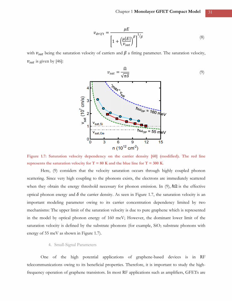
with 119907119904119886119905 being the saturation velocity of carriers and 120573 a fitting parameter The saturation velocity
119907119904119886119905 is given by [46]
119907119904119886119905 =Ω
radic120587120575 (9)
Figure 17 Saturation velocity dependency on the carrier density [60] (modified) The red line
represents the saturation velocity for T = 80 K and the blue line for T = 300 K
Here (9) considers that the velocity saturation occurs through highly coupled phonon
scattering Since very high coupling to the phonons exists the electrons are immediately scattered
when they obtain the energy threshold necessary for phonon emission In (9) ℏΩ is the effective
optical phonon energy and 120575 the carrier density As seen in Figure 17 the saturation velocity is an
important modeling parameter owing to its carrier concentration dependency limited by two
mechanisms The upper limit of the saturation velocity is due to pure graphene which is represented
in the model by optical phonon energy of 160 meV However the dominant lower limit of the
saturation velocity is defined by the substrate phonons (for example SiO2 substrate phonons with
energy of 55 meV as shown in Figure 17)
4 Small-Signal Parameters
One of the high potential applications of graphene-based devices is in RF
telecommunications owing to its beneficial properties Therefore it is important to study the high-
frequency operation of graphene transistors In most RF applications such as amplifiers GFETs are
32 Chapter 1 Monolayer GFET Compact Model
operated in the ON state and an AC small-signal is used as input The RF performance of a GFET is
characterized in terms of its small-signal parameters such as the transconductance 119892119898 the output
conductance 119892119889119904 the gate-to-source capacitance 119862119866119878 and the gate-to-drain capacitance 119862119866119863
Thereby an accurate model is required to precisely represent the mutual capacitances among the
gate source and drain
C) The Electrical Compact Models
Following the research in the last few years which is expected to continue in the near future
graphene has been studied to develop system level integrated circuits Thus itrsquos highly desirable to
develop a physics-based model capable of providing insight into the carrier transport in graphene
devices As a consequence several models have been developed in the last few years which can be
divided into two major groups physical models and analytical models
Physical models [62]ndash[69] provide a better understanding of the carrier transport in the
GFET devices However being physics-based their computation time is distinctly higher and their
implementation complicated To name a few Pugnaghi et al [62] proposed a semi-analytical model
for GFETs in the ballistic limit and Champlain [63] presented a theoretical examination of thermal
statistics electrostatics and electrodynamics of GFETs Moreover in [64] Champlain presented a
small-signal model for GFETs derived from a physical description of the GFETs operation Ryzhii et
al [65] presented a device model that includes the Poisson equation with the weak nonlocality
approximation Thiele et al [66] considered a different modeling approach in which the drain voltage
is obtained for a given drain current into the device
Analytical models [46] [70]ndash[87] provide sufficient accuracy while considerably reducing the
computation time A common form of analytical models which is often used by designers for the
ease of integration into circuit design flow is an electrical compact model The compact models are
sufficiently simple and accurate in order be implemented in standard simulators useful for circuit
designers and computer aided design Figure 18 shows the evolution of the different analytical
models in the last few years IMS Laboratory from University of Bordeaux has been a major
contributor in providing accurate compact models for GFETs since 2012
33 Chapter 1 Monolayer GFET Compact Model
Figure 18 Timeline of Compact Model Development
In addition Table 1 summarizes the key characteristics of each of the models mentioned
above It also highlights where this work stands relative to the models developed thus far
Thiele et al Quasi-analytical model for DC simulation and a Compact Model for
Small-Signal simulation
Nov 2008 May 2010 May 2011 Dec 2011
Meric et al Quasi-analytical model based on the Drift-Diffusion equation
Wang et al Compact Model based on the Virtual Source
model for Si MOSFETs
Jiacutemenez et al Compact Model based on the Drift-Diffusion equation with 9 non-reciprocal capacitances for transient and small-signal simulations
April 2012 May 2012
Habibpour et al Compact Model based on the Drift-Diffusion equation with the possibility of S-Parameter and Power Spectrum Simulation
Henry et al Compact Model based on the Drift-Diffusion equation for monolayer and bilayer GFETs
Parrish et al Compact Model based on the Drift-Diffusion equation in the quantum capacitance limit
Freacutegonegravese et al Scalable Compact Model based on the Drift-Diffusion equation
April 2014 July 2014
Rodriacuteguez et al Compact model based on the Drift-Diffusion equation for fast hand calculations of figures
of merit
Umoh et al Compact Model based on the Drift-Diffusion equation for an arbitrary number of graphene layers
Rakheja et al Compact Model based on the Drift-Diffusion equation for quasi-ballistic GFETs
Landauer et al Compact Model based on the Drift-Diffusion equation with improved accuracy around the Dirac point
March 2015 Oct 2015 May 2016 June 2016
Mukherjee et al Compact Model based on the Drift-Diffusion equation including aging laws and failure mechanisms
Tian et al Compact model based on the Drift-Diffusion equation with improved accuracy around the Dirac point for the quantum capacitance and the saturation velocity
Pasadas et al Compact charge-based intrinsic capacitance model for double-gate four-terminal GFETs with 16 capacitances including self-capacitances and
transcapacitances
This work Accurate physics-based large signal compact model for MGFETs Extension of model capabilities to AC and transient circuit simulations by introducing an accurate description of the gate capacitances (CGS and CGD) Electromagnetic simulations of the entire GFET structure for extraction of parasitic elements
July 2012 July 2012 July 2012
Sept 2014 Sept 2014
This work Accurate physics-based large signal compact model for m-GFETs Extension of model capabilities to AC and transient circuit simulations by introducing accurate descriptions of the gate capacitances (CGS and CGD) Electromagnetic simulations of the entire GFET structure for extraction of parasitic elements
34 Chapter 1 Monolayer GFET Compact Model
Table 1 Summary of GFET Compact Model Development
Author Quantum
Capacitance
Different electron and
hole mobilities
Access Resistances
Effect of the Back-Gate
Saturation Velocity
RF Simulation RF Comparison
with Measurement
Meric et al [46] Cq α radicn No No Yes Yes carrier
concentration dependent
No No
Thiele et al [70] Cq α |VCH| No Yes fitting parameters
Yes Yes carrier
concentration dependent
No No
Wang et al [71] Yes
Yes tunable through the effect of the
back-gate
Yes Yes No No
Jiacutemenez et al [72] [73]
Cq α |VCH| No Yes fitting parameters
Yes
Yes carrier concentration
dependent in [72] No in [73]
It presents nine non-reciprocal
capacitances for transient and small-signal simulation
No comparison with measurements
Habibpour et al [74]
Cq ≫ Ctop valid except for
ultrathin top-gate dielectrics
Yes
Different contact
resistances are
considered when the
channel is n- or p-type
No Yes carrier
concentration dependent
Yes S-Parameter and Power Spectrum Measurements
Henry et al [75] Cq α radicn No
Yes Schottky barrier
effective resistances
Yes Yes carrier
concentration dependent
No No
Parrish et al [76] Cq ≪ Ctop in the
quantum capacitance
No No No Yes considered to
be material constant
No No
35 Chapter 1 Monolayer GFET Compact Model
limit
Freacutegonegravese et al [77] [78]
Cq α |VCH| No Yes fitting parameters
No Yes carrier
concentration dependent
Yes Yes
Rodriacuteguez et al [79]
Cq α |VCH| No Yes fitting parameters
No Yes carrier
concentration dependent
Yes No
Umoh et al [80]
Separate quantum
capacitances (Cqα |VCH|) for
each layer separated by
interlayer capacitances
Yes
Yes fitting parameters
different for holes and electrons
Yes No No No
Rakheja et al [81] Cq α radicVCH2 No
Yes different contact
resistances for n- and p-type channels
Yes Yes No No
Landauer et al [82]
Weighting function for the
quantum capacitance to
improve accuracy around the Dirac point
No Yes constant
contact resistances
Yes Yes two region
model No No
Mukherjee et al [83]
Cq α |VCH| Yes
Yes differential resistances across the Schottky junction
Yes Yes carrier
concentration dependent
No No
Tian et al [84]
Weighting function for the
quantum capacitance to
Yes carrier density
dependent mobilities
Yes fitting parameters
Yes
Yes approximation fitting the two
region model by
No No
36 Chapter 1 Monolayer GFET Compact Model
improve accuracy around the Dirac point
[82]
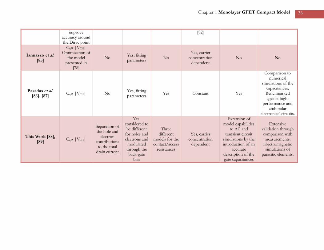
Iannazzo et al [85]
Cq α |VCH| Optimization of
the model presented in
[78]
No Yes fitting parameters
No Yes carrier
concentration dependent
No No
Pasadas et al [86] [87]
Cq α |VCH| No Yes fitting parameters
Yes Constant Yes
Comparison to numerical
simulations of the capacitances Benchmarked against high-
performance and ambipolar
electronicsrsquo circuits
This Work [88] [89]
Cq α |VCH|
Separation of the hole and
electron contributions to the total
drain current
Yes considered to be different
for holes and electrons and
modulated through the back-gate
bias
Three different
models for the contactaccess
resistances
Yes carrier concentration
dependent
Extension of model capabilities
to AC and transient circuit
simulations by the introduction of an
accurate description of the gate capacitances
Extensive validation through comparison with measurements
Electromagnetic simulations of
parasitic elements
37 Chapter 1 Monolayer GFET Compact Model
D) A Large-Signal Monolayer Graphene Field-Effect Transistor
Compact Model for RF-Circuit Applications (This Work) [88] [89]
Despite being in an early stage of development several works targeting high-frequency
applications using graphene-based devices have been proposed such as amplifiers [33]ndash[35] mixers
[36]ndash[40] frequency receivers [41] ring oscillators [42] terahertz detectors [43] [44] and even balun
architectures [45] With the continuing development of graphene-based RF circuits models that are
able to accurately describe the GFET behavior in the high frequency domain are quite essential
To address these issues in this work an accurate physics-based large signal compact model
for m-GFETs suitable for both DC and RF circuit simulations is presented Since the devices
considered in this work have lengths higher than 100 nm the presented compact model is based on
the classical drift-diffusion transport approach The proposed model has been implemented in
Verilog-A A separation of the hole and electron contributions to the total drain current has been
considered without diminishing the accuracy around the Dirac point in addition to an improved
accuracy in the branch current descriptions In addition the effect of the back-gate on the induced
carrier density and access resistances is considered Furthermore the model capabilities have been
extended to AC and transient circuit simulations by including an accurate description of the gate
capacitances (119862119866119878 and 119862119866119863) Electromagnetic (EM) simulations of the entire GFET structure have
been performed to extract the values of the parasitic elements
The compact model is based on the conventional dual-gate FET structure presented in
Figure 14 The back-gate stack includes the back-gate dielectric and the substrate The different
model components are described in the following subsections
1 The Carrier Densities
Considering Fermi-Dirac distribution and based on the 2-D DOS of monolayer graphene in
(5) the 2-D electron and hole gas sheet densities in graphene can be written as
119899 = int ρGr sdot 119891119865119863(119864)119889119864 =
+infin
0
2
120587(ℏ119907119865)2int
119864
1 + exp (119864 minus 119864119865119896119861119879
)119889119864
+infin
0
(10)
119901 = intρGr sdot [1 minus 119891119865119863(119864)]119889119864 =
0
minusinfin
2
120587(ℏ119907119865)2int
119864
1 + exp (119864 + 119864119865119896119861119879
)119889119864
+infin
0
(11)
38 Chapter 1 Monolayer GFET Compact Model
where 119891119865119863 is the Fermi-Dirac distribution 119896119861 the Boltzmann constant 119879 the room temperature and
119864119865 the Fermi level
Under the effect of a given set of bias conditions a voltage drop 119881119862119867(119909) across the
quantum capacitance 119862119902 is created The channel voltage 119881119862119867(119909) along the channel at a distance 119909
causes a variation in the Fermi level Here the Fermi level is considered to vary proportionally with
the channel voltage and thus 119864119865 = 119902 sdot 119881119862119867 where 119902 is the electronic charge The net carrier sheet
density 119876119899119890119905 stored in the quantum capacitance can be written as
119876119899119890119905(119909) = 119902 sdot (119901 minus 119899) = 119876119901 minus 119876119899 =2119902
120587(119896119861119879
ℏ119907119865)2
[1198651198651198631(120578) minus 1198651198651198631(minus120578)] (12)
where 119865119865119863119895 is the Fermi-Dirac integral for an order 119895 given by
119865119865119863119895(120578) =1
Γ(119895 + 1)int
120583119895
1 + exp(120583 minus 120578)119889120583
+infin
0
(13)
with 120578 = 119864
119896119861119879 and 120583 = 119864119865
119896119861119879 Γ(119899) = (119899 minus 1) is the Gamma function
2 The Quantum Capacitance
The quantum capacitance 119862119902 accounts for the finite Density of States in a material
Therefore 119862119902 is in series with the geometric electrostatic top-gate capacitance Because of the low
values of 119862119902 in graphene it has a considerable impact in the total gate-capacitance The quantum
capacitance is defined as the derivative of the net carrier sheet density 119876119899119890119905 with respect of the
channel voltage 119881119862119867 as in an ordinary capacitor and it can be written as in (6) However to
considerably simplify the electrostatics calculations it is helpful to assume 119902 sdot |119881119862119867| ≫ 119896119861119879 and thus
the quantum capacitance can be written as [49]
119862119902(119909) =21199022119896119861119879
120587(ℏ119907119865)2ln 2 [1 + cosh(
119902119881119862119867(119909)
119896119861119879)]
119902sdot119881119862119867≫119896119861119879rArr 119862119902 =
21199022
120587
119902 sdot |119881119862119867(119909)|
(ℏ119907119865)2
(14)
Yet in the vicinity of Dirac point (14) underestimates the carrier density (Figure 19)
resulting in a diminished accuracy Nonetheless in order to keep the compact model simple the
quantum capacitance is further considered to vary linearly as a function of the channel voltage as
suggested by (14)
Finally under this approximation the net carrier density 119876119899119890119905 is written as
119862119902(119909) = minus119889119876119899119890119905(119909)
119889119881119862119867rArr 119876119899119890119905(119909) = minusint119862119902 119889119881119862119867 = minus
1199022
120587
119902 sdot |119881119862119867|119881119862119867(ℏ119907119865)2
(15)
39 Chapter 1 Monolayer GFET Compact Model
The negative sign of 119862119902 in (15) can be explained as follows [70] a more positive gate voltage
and in turn a more positive 119881119862119867 leads to a more negative charge in the graphene channel
Figure 19 Quantum Capacitance Cq versus Channel Voltage VCH
3 The Channel Voltage
Considering the GFET structure in Figure 14 an equivalent capacitive circuit can be
established as in Figure 110
Figure 110 Equivalent capacitive circuit of the m-GFET structure
In Figure 110 119881119866119878119894 and 119881119861119878119894 represent the top-gate-to-source voltage and the intrinsic back-
gate-to-source intrinsic voltages respectively 119881119862119867 represents the voltage across the quantum
capacitance and 119881(119909) the voltage drop in the graphene channel due to intrinsic drain-to-source
voltage 119881119863119878119894 119881(119909) varies from 119881(0) = 0 at 119909 = 0 to 119881(119871) = 119881119863119878119894 at 119909 = 119871
Applying Kirchhoffrsquos relation to the equivalent capacitive circuit shown in Figure 110 the
following can be written
-050 -025 000 025 050000
005
010
015
Qu
an
tum
Cap
acit
an
ce
Cq [
F
m2]
Channel Voltage VCH
[V]
Exact Cq
Approximation Cq
40 Chapter 1 Monolayer GFET Compact Model
119876119899119890119905(119909) + 119902 sdot 119873119865 = (119876119879119866(119909) + 119876119861119866(119909)) (16)
where 119876119879119866(119909) and 119876119861119866(119909) are top-gate and back-gate induced charges given by
119876119879119866(119909) = 119862119905119900119901 sdot [119881119866119878119894 minus 119881(119909) minus 119881119862119867(119909)] (17)
119876119861119866(119909) = 119862119887119886119888119896 sdot [119881119861119878119894 minus 119881(119909) minus 119881119862119867(119909)] (18)
119873119865 accounts for the additional charge due to impurities or doping of the channel 119862119905119900119901 =
0 119905119900119901
119905119905119900119901 and 119862119887119886119888119896 =
0 119887119886119888119896
119905119887119886119888119896 are the top- and back-gate capacitances respectively Here (휀119905119900119901 휀119887119886119888119896)
and (119905119905119900119901 119905119887119886119888119896) are the dielectric constants and thicknesses of the dielectric layers Based on (15)-
(18) a second-degree equation for the channel voltage can be written and its solutions are given by
119881119862119867(119909) = sign (119876119905119900119905 minus 119862119890119902119881(119909))
minus119862119890119902 + radic1198621198901199022 + 4120572|119876119905119900119905 minus 119862119890119902119881(119909)|
2120572
(19)
with 120572 =1199023
120587(ℏ119907119865)2 119862119890119902 = 119862119905119900119901 + 119862119887119886119888119896 119876119905119900119905 = 119876119905119900119901 + 119876119887119886119888119896 +119876119865 119876119905119900119901 = 119862119905119900119901119881119866119878119894 119876119887119886119888119896 =
119862119887119886119888119896119881119861119878119894 and 119876119865 = 119902119873119865
Because of the absence of energy bandgaps in graphene ambipolar conduction in m-GFET
devices is not uncommon Unlike conventional MOSFET devices where the charges responsible for
the drain current are either holes for p-MOSFETs or electrons for n-MOSFETs in ambipolar
devices the conduction across the graphene channel is assisted by either electrons (forall119909 isin
[0 119871] 119881119862119867(119909) gt 0) holes (forall119909 isin [0 119871] 119881119862119867(119909) lt 0) or a combination of both (exist1199090 isin
[0 119871] 119881119862119867(1199090) = 0) This implies that the channel voltage 119881119862119867(119909) determined from the bias
conditions as depicted in (19) controls whether the channel is n-type p-type or ambipolar
Considering the channel voltage 119881119862119867 to be positive the channel is full of electrons and thus
the following can be assumed based on (15)
119876119899119890119905(119909) = 119876119901(119909) minus 119876119899(119909) asymp minus119876119899(119909) rArr 119876119899(119909) = 120572119881119862119867
2
119876119901(119909) asymp 0 (20)
where 119876119899 and 119876119901 are the hole and electron charge contributions respectively Figure 111a is a
representative image with standard values displaying the net carrier density 119876119899119890119905 and the channel
voltage 119881119862119867 variation along the channel
Similarly when 119881119862119867 is negative and thus the channel is full of holes the following
approximation is valid
119876119899119890119905(119909) = 119876119901(119909) minus 119876119899(119909) asymp 119876119901(119909) rArr 119876119901(119909) = 1205721198811198621198672 (21)
41 Chapter 1 Monolayer GFET Compact Model
119876119899(119909) asymp 0
Similarly Figure 111b illustrates the channel voltage and the net carrier density when the
channel is p-type
Figure 111 GFET channel conditions a) n-type channel b) p-type channel c) n-type to p-type
channel and d) p-type to n-type channel CNP is the charge neutrality point
42 Chapter 1 Monolayer GFET Compact Model
However when (exist1199090 isin [0 119871] 119881119862119867(1199090) = 0) is valid ambipolar conduction occurs
Considering the case in Figure 111c where a transition occurs from an n-type channel to a p-type
channel the following expressions can be written
forall119909 isin [0 1199090) 119881119862119867(119909) gt 0 rArr 119876119899(119909) = 120572119881119862119867
2 (119909) and 119876119901(119909) = 0
forall119909 isin (1199090 119871] 119881119862119867(119909) lt 0 rArr 119876119901(119909) = 1205721198811198621198672 (119909) and 119876119899(119909) = 0
(22)
Equivalently when a transition occurs from a p-type channel to an n-type channel (Figure
111d) the following can be assumed
forall119909 isin [0 1199090) 119881119862119867(119909) gt 0 rArr 119876119901(119909) = 120572119881119862119867
2 and 119876119899(119909) = 0
forall119909 isin (1199090 119871] 119881119862119867(119909) lt 0 rArr 119876119899(119909) = 1205721198811198621198672 and 119876119901(119909) = 0
(23)
4 The Drain-to Source Current
Based on the drift-diffusion theory of transport the drain-to-source current 119868119863119878 can be
written as
119868119863119878 = minus119882 sdot 119876(119909) sdot 119907119889119903119894119891119905(119909) (24)
where 119876(119909) is the carrier density in the channel at a position 119909 from the source 119907119889119903119894119891119905(119909) is the drift
velocity of carriers and 119882 the gate width In (24) the drain-to-source current is assumed to be
constant at any point 119909 in the channel
Considering a soft-saturation of the drift velocity as in (8) and assuming 120573 = 1 (24) is further written as
119868119863119878 = minus119882 sdot 119876(119909) sdot
120583119864
1 +120583|119864|119907119904119886119905
119864=minus119889119881(119909)
119889119909
rarr minus119882 sdot 119876(119909) sdot120583 (minus
119889119881(119909)119889119909
)
1 +120583 |minus
119889119881(119909)119889119909
|
119907119904119886119905
(25)
where 120583 is the average carrier mobility
Integrating by separation of the x-dependent terms on one side and V-dependent terms on
the other side the drift-diffusion drain-to-source current 119868119863119878 is given by
119868119863119878 = 120583119882int |119876| 1198891198811198811198631198781198940
119871 + 120583 |int1119907119904119886119905
1198891198811198811198631198781198940
| (26)
Although (26) considers an average carrier mobility 120583 that accounts for most of the
ambipolar GFET operations in several cases different electron and hole transport behavior in the
graphene channel is observed and expression (26) is no longer valid To expand the model
capabilities and account for an asymmetric conduction behavior different mobilities for holes and
43 Chapter 1 Monolayer GFET Compact Model
electrons must be considered implying different levels of contribution to the total drain current To
consider the aforementioned the total drain current has been assumed to be the sum of the electron
and hole contributions
119868119863119878 = 119868119863119878119899 + 119868119863119878119901 (27)
Equation (27) is used specifically to account for the ambipolar conduction in the graphene
channel The total current is the sum of the electron and hole currents and the calculation of the 119868119863119878119899
and 119868119863119878119901 are self-consistent regarding the direction of the current flow for each branch Considering
for example when the channel is entirely n-type and the current flows from the drain to source for
119881119866119878 and 119881119863119878 both being positive On the other hand for the same 119881119863119878 if 119881119866119878 becomes sufficiently
negative the channel becomes entirely p-type and holes are pushed from the drain to the source
maintaining the same direction of the hole current as that of the electron In either of these cases
there is negligible contribution of the minority carrier that also has the same direction of current flow
as that of the majority carriers Lastly when 119881119866119878 asymp 119881119863119894119903119886119888 the charge neutrality point is located
within the channel and the same direction for the electron and hole currents is maintained In
addition to this a significant electron-hole recombination takes place which however does not cause
energy dissipation due to the gapless nature of graphene
5 The Residual Carrier Density
Scanning Tunneling Microscopy (STM) studies [90] [91] have shown the presence of
electron and hole puddles in the graphene layer These electron and holes puddles are the result of
the inevitable presence of disorder in the graphene layer They account for the anomalously finite
conductivity however minimal observed around the Dirac point This unexpected behavior has
been attributed to first mesoscopic corrugations (ripples) [92] [93] leading to a fluctuating Dirac
point and second to charged impurities leading to an inhomogeneous carrier density [94] [95]
Considering that the areas of the hole and electron puddles are equal in size the spatial
electrostatic potential is simplified as a step function with a peak to peak value of plusmnΔ as shown in
Figure 112 The residual carrier density due to electron and hole puddles is written as
119899119901119906119889119889119897119890 =Δ2
120587(ℏ119907119865)2 (28)
44 Chapter 1 Monolayer GFET Compact Model
Figure 112 Spatial inhomogeneity of the electrostatic potential [96]
6 The Parasitic Series Resistances
As described in Section B) the parasitic series resistances including the access resistances and
contact resistances are important parameters that need to be properly modelled as they represent a
serious issue leading to degradation of the GFET performance especially when the device
dimensions are scaled down [97] In fact scaling down the channel increases the drain current level
while the parasitic series resistances are not scaled down and eventually the parasitic series resistance
can dominate the total resistance in highly scaled devices Moreover most of the GFET devices have
access resistances which are not optimized ie the graphene in the access regions has a low carrier
density (given by the quality of graphene and process) leading to a highly resistive access In order to
increase the carrier density within the access regions one can build a back-gate or generate defects in
the access region [98]
Thereby here three different models (empirical Schottky barrier height and Back-Gate
charge modulation) are proposed to accurately describe the effect of the parasitic series resistances
119877119878 and 119877119863 on the GFET performance For ease of implementation and as a first attempt an
empirical model has been developed in order to account for the different access resistance whether
the graphene in the sourcedrain access region is n-type or p-type Later in order to give a physical
interpretation to the empirical model a Schottky barrier model has been developed In this model
the access resistances are modeled as a function of the barrier height between the metal and the
graphene interface accounting for different graphene sheet polarities Moreover a third model has
been proposed accounting for the charge modulation in the access regions due to the effect of the
back-gate voltage In the following the proposed models for the parasitic series resistances are
described in detail
45 Chapter 1 Monolayer GFET Compact Model
a) Empirical Model
This model considers that because of the back-gate effects as well as due to possible doping
during the metallization the graphene regions underneath the metal contacts can be either n-type or
p-type and thus a junction is formed at the drain and the source sides It follows that depending on
the channelrsquos polarity different parasitic series resistances need to be considered For this first an
empirical model is considered based on a smoothing function which considers a transition between a
resistance 119877(119878119863)1198990 when the channel is n-type and a resistance 119877(119878119863)1199010 when the channel is p-type
The aforementioned smoothing function can be written empirically as
119891119878119898119877 =
1
1 + exp(119868119863119878119899 minus 119868119863119878119901
120593 )
(29)
where 119868119863119878119899 and 119868119863119878119901 are the electron and hole contributions to the drain current respectively and 120593
is a fitting parameter The width-normalized source and drain parasitic series resistances are given by
1198771198780 = 1198771198781198990 sdot (1 minus 119891119878119898119877) + 1198771198781199010 sdot 119891119878119898119877
1198771198630 = 1198771198631198990 sdot (1 minus 119891119878119898119877) + 1198771198631199010 sdot 119891119878119898119877 (30)
b) Schottky Barrier Model
The parasitic series resistances are considered to be different according to whether the
channel is n-type or p-type The contact resistances can be modeled as a function of the barrier
height Φ119861 between the metal and the graphene interface The barrier height changes with the
graphene sheet polarity ie on either side of the Dirac point and hence different barrier heights are
considered in case of the electron (Figure 113a) and the hole carriers (Figure 113b)
Figure 113 Schottky junction formation between the metal and a) n-type or b) p-type graphene
channel
46 Chapter 1 Monolayer GFET Compact Model
Assuming the Richardsonrsquos model for the Schottky junction current it can be written as [99]
[100]
119868 = 119860lowast1198792exp (minus119902ΦB119896119861119879
) [exp (minus119902119881119860119896119861119879
) minus 1] (31)
with 119881119860 being the applied voltage across the junction and 119860lowast the Richardsonrsquos constant The
differential resistance is given as
119903 = [119902119860lowast119879
119896119861exp (minus
119902Φ119861119896119861119879
) exp (minus119902119881119860119896119861119879
)]minus1
= 1199030 exp (119902Φ119861119896119861119879
) (32)
Therefore here the source and drain parasitic resistances can be written as a sum of the
differential resistances across the Schottky junction and the metal contact resistance Considering
the graphene in the source access region to be n-type the source parasitic resistance is given by
1198771198780 = 1198771198621198780 + 1199031198780119899exp (
119902Φ119861119878119899119896119861119879
) (33)
where Φ119861119878119899 is the barrier height between the metal and the graphene(n-type) interface in the source
access region Equivalently when the source access region is p-type the source parasitic resistance is
1198771198780 = 1198771198621198780 + 1199031198780119901exp (
119902Φ119861119878119901119896119861119879
) (34)
where Φ119861119878119901 is the barrier height between the metal and the graphene (p-type) interface in the source
access region Similarly in the drain access region the parasitic series resistance when the drain
access region is n-type or p-type is given respectively by
1198771198630 = 1198771198621198630 + 1199031198630119899 exp (119902Φ119861119863119899119896119861119879
) (35)
1198771198780 = 1198771198621198630 + 1199031198630119899 exp (119902Φ119861119863119899119896119861119879
) (36)
where (1198771198621198780 1198771198621198630) are the source and drain contact resistances due to the metal respectively
(1199031198780119899 1199031198630119899 1199031198780119901 1199031198630119901 ) are functions of the voltage difference (119881119860) across the access region but for
simplicity they are assumed to be model parameters considering transfer lengths under the contacts
to be insignificant
47 Chapter 1 Monolayer GFET Compact Model
c) Back-Gate Charge Modulated Series Resistances
In the drain and source access regions contact resistances (1198771198621198780 1198771198621198630) as well as vertical
electric-field-induced modulation of the access resistances (119877119878119860119888 119877119863119860119888) are considered The applied
vertical electric field results in the modulation of the charge density in the graphene access regions
uncovered by the top-gate stack thereby these access resistances are only affected by the back-gate
and vary independently of the top-gate voltage
Based on the applied bias conditions an equivalent capacitive circuit of the m-GFET
structure in the access regions is shown in Figure 114 In the source access region a Kirchhoffrsquos
relation based on the equivalent capacitive circuit shown in Figure 114a can be written as follows
119876119878 + 119902 sdot 119873119865119878 = minus119876119861119878 (37)
where 119876119878 is the charge stored in the quantum capacitance given by (15) 119873119865119878 is the net doping of the
graphene layer in the access region and 119876119861119878 is the back-gate induced charge given by
119876119861119878 = 119862119887119886119888119896 sdot (119881119861119878119894 minus 119881119862119867119861119878) (38)
with 119881119862119867119861119878 being the voltage across the quantum capacitance in the source access region
Figure 114 Equivalent capacitive circuit of the m-GFET a) source and b) drain access
regions
Based on (37)-(38) a second degree equation for 119881119862119867119861119878 can be written and its solutions are
given by
119881119862119867119861119878 = sign(119876119905119900119905119878)
minus119862119887119886119888119896 +radic1198621198871198861198881198962 + 4120572|119876119905119900119905119878|
2120572
(39)
with 119876119905119900119905119878 = 119876119887119886119888119896119878 + 119876119865119878 119876119887119886119888119896119878 = 119862119887119886119888119896119881119861119878119894 and 119876119865119878 = 119902119873119865119878
48 Chapter 1 Monolayer GFET Compact Model
When electrons are accumulated in the source access region (119881119862119867119861119878 gt 0) the self-consistent
solutions of equations (37) and (39) allows the calculation of the net charge density in the access
region 119876119878 The resistance of the source access region is assumed to vary inversely with the induced
carrier density due to the effect of the back-gate bias Thus the width-normalized parasitic series
resistance can be written as the sum of contact resistance and the modulated access resistance as
1198771198780 = 1198771198781198880 +119871119878
120583119899119878(|119876119878| + 119902 sdot 119899119861119878) (40)
where 120583119899119878 is the mobility of electrons in the source region 119899119861119878 is a residual charge density in the
access region and 119871119878 is the source access length
Similarly when holes are accumulated in the source access region (119881119862119867119861119878 lt 0) the width-
normalized parasitic series resistance is written as
1198771198780 = 1198771198781198880 +119871119878
120583119901119878(|119876119878| + 119902 sdot 119901119861119878) (41)
Here 120583119901119878 is the hole mobility in the source region and 119901119861119878 is the residual charge density in
the access region
Similarly to the formulations of the equations (37)-(41) equations for the drain parasitic
series resistances can be established based on the equivalent capacitive circuit shown in Figure 114b
7 Gate resistance - Scalable Model
Developing a scalable model is as desirable as it is important for identifying the physical
parameters dominantly affected by scaling Here the model is scaled with respect to the channel
length 119871 the channel width 119882 and the number of fingers 119873ℱ119899119892 The effect of the gate resistance is
significant in RF range as it could lead to an increased thermal noise as well as a reduction of the
maximum available gain The gate resistance depends directly on the physical structure (layout) of the
device and at high frequency it can be modeled as a distributed R-C circuit Thus based on
transmission-line theory the gate resistance is given by
119877119892 = 119877119904ℎ119882
3119871119873ℱ119899119892 (42)
where 119877119904ℎ is the gate sheet resistance in Ω
49 Chapter 1 Monolayer GFET Compact Model
8 Gate Capacitances
To extend the model capabilities to AC and transient circuit simulations an accurate
description of the gate-to-source 119862119866119878 and the gate-to-drain 119862119866119863 capacitances also needs to be
incorporated in the model
First an explicit dependence of the total charge in the channel needs to be derived as a
function of the node voltages (119881119866119878119894 119881119861119878119894 119881119863119878119894) and thus given as follows
119876119888ℎ119886119899119899119890119897 = 119882int(119876119899119890119905 + 119902 sdot 119899119901119906119889119889119897119890) 119889119909
119871
0
(43)
where 119899119901119906119889119889119897119890 is the residual carrier density due to puddle formation as described in Section 5 For a
finite drain-to source voltage 119881119863119878119894 the total gate capacitance is defined as follows [101]
119862119866119866 = 119862119866119878 + 119862119866119863 = (120597119876119888ℎ119886119899119899119890119897120597119881119866119878119894
)119881119863119878119894=119888119900119899119904119905119886119899119905
(44)
Based on (44) and considering that 119881119866119863119894 = 119881119866119878119894 minus 119881119863119878119894 the gate-to-source 119862119866119878 and gate-to-drain
119862119866119863 capacitances can be written as
119862119866119863 = (120597119876119888ℎ119886119899119899119890119897120597119881119866119863119894
)119881119866119878119894=119888119900119899119904119905119886119899119905
= minus(120597119876119888ℎ119886119899119899119890119897120597119881119863119878119894
)119881119866119878119894=119888119900119899119904119905119886119899119905
(45)
119862119866119878 = (120597119876119888ℎ119886119899119899119890119897120597119881119866119878119894
)119881119863119878119894=119888119900119899119904119905119886119899119905
+ (120597119876119888ℎ119886119899119899119890119897120597119881119863119878119894
)119881119866119878119894=119888119900119899119904119905119886119899119905
(46)
A simplified large-signal circuit representation of the intrinsic transistor is given in Figure
115 The bulk connection has been omitted for sake of clarity Doing so the total capacitances
between the back-gate and the source and the back-gate and the drain are neglected In fact
considering a thick back-gate dielectric which is usually the case the following equation can be
written
1
119862119890119902=
1
119862119887119886119888119896+1
119862119902asymp
1
119862119887119886119888119896 (47)
50 Chapter 1 Monolayer GFET Compact Model
Figure 115 Intrinsic Large-Signal Equivalent Circuit
Moreover in Figure 115 119876119866119863 and 119876119866119878 are the gate-to-drain and gate-to-source charges
respectively given by
119876119866119863 = 119862119866119863 sdot 119881119866119863119894 (48)
119876119866119878 = 119862119866119878 sdot 119881119866119878119894 (49)
9 Numerical Model [102]
In addition to the compact model a numerical model (OctaveMatlab) has additionally been
developed The numerical model is based on
Non-linear System Solver
Trapezoidal Numerical Integration
Numerical Differentiation
This numerical model is implemented using the exact solution of the quantum capacitance in
(6) and thus the compact model has been benchmarked against the numerical model to evaluate its
accuracy particularly due to the considered simplifications Figure 116 shows a block diagram
describing the implementation of the numerical model Moreover the numerical model allows the
extraction of intermediate variables such as the variation of the channel voltage the saturation
velocity and the carrier density along the channel However the numerical model being an iterative
model with self-consistent calculations the computation time becomes considerably higher
compared to that of the compact model
51 Chapter 1 Monolayer GFET Compact Model
Figure 116 Numerical Model Block Diagram the model utilizes three main functions lsquofsolversquo to
solve non-linear system equations lsquotrapzrsquo to calculate numerical integrations and lsquodiffrsquo to perform
numerical differentiations
10 Compact Model Implementation
Developing compact models for standard circuit simulators implies developing analytical
equations to accurately represent the internal physics of the device In this section the
implementation of the model is described in accordance with the definitions in previous sections
The model equations have been implemented in Verilog-A for it to be fully compatible with standard
circuit simulators
a) The Drain-to-Source Current
The total drain-to-source current is considered to be sum of the electron and hole
contributions which based on (26) and (28) are written as
Physical Parameters Bias Conditions Other Parameters
Intrinsic Voltages
Channel Potential
Carrier Densities Saturation Velocity
Carrier Integrals Saturation Velocity IntegralsDrain-to-Source Current
52 Chapter 1 Monolayer GFET Compact Model
119868119863119878(119899119901) = 120583(119899119901)119882int(|119876(119899119901)| + 119902 sdot
1198991199011199061198891198891198971198902 ) 119889119881
119871 + 120583(119899119901) |int1
119907119904119886119905(119899119901) 119889119881|
(50)
with 120583(119899119901) being the electronhole mobility Following from (9) 119907119904119886119905(119899119901) the electronhole
concentration-dependent saturation velocity is given by
119907119904119886119905(119899119901) =Ω
radic120587 (|119876(119899119901)|119902
+1198991199011199061198891198891198971198902
)
(51)
The term 119899119901119906119889119889119897119890 2frasl in (50) and (51) accounts for an even distribution of the residual carrier
density in electron and hole puddles
Eq (19) indicates that the sign of 119881119862119867(119909) is determined by the sign of the term
119911(119909) = 119876119905119900119905 minus 119862119890119902119881(119909) (52)
Thereby as explained in Section 3 if 119911(119909 = 0) and 119911(119909 = 119871) both remain positive the
channel polarity is n-type and the current conduction is supported mostly by electrons (Figure 111a)
Therefore based on (20) and (26) the electron and hole current contributions are written as
119868119863119878119899 = 120583119899119882int (120572119881119862119867
2 + 119902 sdot1198991199011199061198891198891198971198902 ) 119889119881
1198811198631198781198940
119871 + 120583119899 |1Ωint radic
120587120572119902 119881119862119867
2 +1205871198991199011199061198891198891198971198902 119889119881
1198811198631198781198940
|
(53)
119868119863119878119901 = 120583119901119882int (119902 sdot
1198991199011199061198891198891198971198902 ) 119889119881
1198811198631198781198940
119871 + 120583119901 |1Ωint
radic1205871198991199011199061198891198891198971198902
1198811198631198781198940
119889119881|
(54)
Similarly when 119911(119909 = 0) and 119911(119909 = 119871) are both negative and the current conduction is
dominated by holes (Figure 111b) expressions for the electron and hole current contributions can
be derived as
119868119863119878119899 = 120583119899119882int (119902 sdot
1198991199011199061198891198891198971198902 ) 119889119881
1198811198631198781198940
119871 + 120583119899 |1Ωint
radic1205871198991199011199061198891198891198971198902
1198811198631198781198940
119889119881|
(55)
119868119863119878119901 = 120583119901119882int (120572119881119862119867
2 + 119902 sdot1198991199011199061198891198891198971198902 ) 119889119881
1198811198631198781198940
119871 + 120583119901 |1Ωint radic
120587120572119902 119881119862119867
2 +1205871198991199011199061198891198891198971198902
1198811198631198781198940
119889119881|
(56)
53 Chapter 1 Monolayer GFET Compact Model
However when 119911(119909 = 0) and 119911(119909 = 119871) are different in sign a change in the carrier type
takes place at the charge neutrality point (119909 = 1199090) within the channel as shown in Figure 111c and
d In these cases the integrals in (50) are separated for two segments of the channel on either side of
the charge neutrality point having opposite polarities
In the case of Figure 111c when a transition from an n-type channel to a p-type channel
exists the electron and hole contributions are expressed as
119868119863119878119899 = 120583119899119882int (120572119881119862119867
2 + 119902 sdot1198991199011199061198891198891198971198902 ) 119889119881
1198810
0+ int (119902 sdot
1198991199011199061198891198891198971198902 ) 119889119881
1198811198631198781198941198810
119871 + 120583119899 |1Ω (int radic
120587120572119902 119881119862119867
2 +1205871198991199011199061198891198891198971198902
1198810
0119889119881 + int radic
1205871198991199011199061198891198891198971198902 119889119881
1198811198631198781198941198810
)|
(57)
119868119863119878119901 = 120583119901119882int (119902 sdot
1198991199011199061198891198891198971198902 ) 119889119881
1198810
0+ int (120572119881119862119867
2 + 119902 sdot1198991199011199061198891198891198971198902 ) 119889119881
1198811198631198781198941198810
119871 + 120583119901 |1Ω(int
radic1205871198991199011199061198891198891198971198902 119889119881
1198810
0+ int radic
120587120572119902 119881119862119867
2 +1205871198991199011199061198891198891198971198902 119889119881
1198811198631198781198941198810
)|
(58)
Equivalent expressions for the electron and hole current contributions when a transition
from a p-type channel to an n-type channel occurs are written as
119868119863119878119899 = 120583119899119882int (119902 sdot
1198991199011199061198891198891198971198902 )119889119881
1198810
0+ int (120572119881119862119867
2 + 119902 sdot1198991199011199061198891198891198971198902 ) 119889119881
1198811198631198781198941198810
119871 + 120583119899 |1Ω (int
radic1205871198991199011199061198891198891198971198902
1198810
0119889119881 + int radic
120587120572119902 119881119862119867
2 +1205871198991199011199061198891198891198971198902 119889119881
1198811198631198781198941198810
)|
(59)
119868119863119878119901 = 120583119901119882int (120572119881119862119867
2 + 119902 sdot1198991199011199061198891198891198971198902 ) 119889119881
1198810
0+ int (119902 sdot
1198991199011199061198891198891198971198902 ) 119889119881
1198811198631198781198941198810
119871 + 120583119901 |1Ω(int radic
120587120572119902 119881119862119867
2 +1205871198991199011199061198891198891198971198902 119889119881
1198810
0+ int radic
1205871198991199011199061198891198891198971198902 119889119881
1198811198631198781198941198810
)|
(60)
where 1198810 is the channel voltage at the charge neutrality point (which can be calculated by equating
119911(119909) to zero thereby yielding to 1198810 = 119876119905119900119905 119862119890119902frasl )
To implement the compact model in Verilog-A analytical solutions for integrals (53)- (60)
have been developed and are presented in Appendix A
b) Gate Capacitances
After some algebraic manipulations (shown in the Appendix A) based on (44)-(46) one can
write
119862119866119866 = minus2120572119882119862119905119900119901int|119881119862119867|
2120572|119881119862119867| + 119862119890119902119889119909
119871
0
(61)
54 Chapter 1 Monolayer GFET Compact Model
119862119866119863 = minus2120572119882119862119890119902119889119881
119889119881119863119878119894int
|119881119862119867|
2120572|119881119862119867| + 119862119890119902119889119909
119871
0
(62)
119862119866119878 = 2120572119882 (119862119890119902119889119881
119889119881119863119878119894minus 119862119905119900119901)int
|119881119862119867|
2120572|119881119862119867| + 119862119890119902119889119909
119871
0
(63)
where 119889119881 119889119881119863119878119894frasl is the rate of change of the potential variation due to 119881119863119878119894 In this work this
quantity has been considered to be a fitting parameter varying from -1 to 1 A common integral term
(referred to as 119868119899119905 in the following) in (61)-(63) can be seen and given by
119868119899119905 = int|119881119862119867|
2120572|119881119862119867| + 119862119890119902119889119909
119871
0
(64)
To calculate this integral the inverse of the electric-field should be introduced 119864 =
minus119889119881(119909) 119889119909frasl which based on (25) can be written as
if 119881119862119867 ge 0 and 119889119909
119889119881ge 0
119889119909
119889119881=120583119899119882
119868119863119878(119876119899 + 119902 sdot 119899119901119906119889119889119897119890) minus
120583119899119907119904119886119905119899
(65)
if 119881119862119867 ge 0 and 119889119909
119889119881lt 0
119889119909
119889119881=120583119899119882
119868119863119878(119876119899 + 119902 sdot 119899119901119906119889119889119897119890) +
120583119899119907119904119886119905119899
(66)
if 119881119862119867 lt 0 and 119889119909
119889119881ge 0
119889119909
119889119881=120583119901119882
119868119863119878(119876119901 + 119902 sdot 119899119901119906119889119889119897119890) minus
120583119901
119907119904119886119905119901 (67)
if 119881119862119867 lt 0 and 119889119909
119889119881lt 0
119889119909
119889119881=120583119901119882
119868119863119878(119876119901 + 119902 sdot 119899119901119906119889119889119897119890) +
120583119901
119907119904119886119905119901 (68)
As depicted from (65)-(68) the term 119889119909 119889119881frasl introduces a mobility-dependence When the
channel is entirely n- or p-type (determined by the sign of 119881119862119867) (61)-(63) consider a single channel
segment for the integrals as in (53)-(56) Consequently for example when 119881119862119867 ge 0 the common
integral term 119868119899119905 while considering unipolar conduction is written as
119868119899119905 = int|119881119862119867|
2120572|119881119862119867| + 119862119890119902sdot [120583(119899119901)119882
119868119863119878(119876(119899119901) + 119902 sdot 119899119901119906119889119889119897119890) minus
120583(119899119901)
119907119904119886119905(119899119901)] 119889119881
119881119863119878119894
0
(69)
On the other hand in case of ambipolar conduction (61)-(63) consider two segments of the
channel having opposite polarities on either side of a transition point (ie 1198810) where the charge
polarity reverses (eg n-type to p-type) as in (57)-(60) Considering as an example the case when a
transition from an n-type to a p-type channel occurs and 119889119909
119889119881ge 0 the integral term 119868119899119905 is written as
55 Chapter 1 Monolayer GFET Compact Model
119868119899119905 = int119881119862119867
2120572119881119862119867 + 119862119890119902sdot [119882
119868119863119878(119876119899 + 119902 sdot 119899119901119906119889119889119897119890) minus
120583119899119907119904119886119905119899
] 119889119881
1198810
0
+ intminus119881119862119867
minus2120572119881119862119867 + 119862119890119902sdot [119882
119868119863119878(119876119901 + 119902 sdot 119899119901119906119889119889119897119890) minus
120583119901
119907119904119886119905119901] 119889119881
119881119863119878119894
1198810
(70)
The solutions for the integrals (61)-(63) are also shown in Appendix A
E) Results amp Discussion
In order to validate the compact model described in the previous sections measurement
results from two relevant m-GFET technologies have been compared with the model simulations
1 Columbia Universityrsquos Device
The first device [46] consists of exfoliated graphene located on a thick SiO2 layer (285 nm)
grown on a heavily doped silicon wafer which acts as a back-gate It has a 15 nm HfO2 top-gate
dielectric (휀119903 = 16) The channel length is 1 microm and the width is 21 microm
Figure 117a presents the comparison between the measured transfer characteristics and the
results from simulation of the compact model and the numerical model A distinct asymmetry of the
hole and electron branches can be observed Additionally the branch currents calculated from the
numerical and the compact models match closely however around the Dirac point a slight
difference is noticeable This difference can be attributed to the usage of a simplified quantum
capacitance equation (14) in the compact model implementation whereas for the numerical model
the exact solution of (6) is considered However taking a closer look the RMS error of the compact
model is found to be 35 whereas for the numerical model it is of 2 therefore from a practical
viewpoint this assumption does not yield a substantial modeling error Also when the drain-to-
source voltage is increased a shift in the Dirac voltage towards more negative top-gate voltages is
observed The maximum achieved IONIOFF current ratio is ~2 which is limited by the gapless nature
of graphene Figure 117b shows the transconductance (119892119898 =119889119868119863119878
119889119881119866119878) of the device depicting good
accuracy between the models even for the second order quantities
56 Chapter 1 Monolayer GFET Compact Model
Figure 117 Comparison of the measured (symbols) a) transfer characteristic (IDS-VGS) and b)
transconductance (gm-VGS) with the numerical model (dashed lines) and the compact model results
(solid lines) for VBS = -40 V and VDS = -05 -10 and -15 V
Figure 118 shows the variation of the channel voltage the carrier densities and the saturation
velocities along the channel for two different top-gate voltages (indicated as vertical dashed lines in
Figure 117a) Considering the plots on the left of Figure 118 for 119881119866119878 = minus2 V and thus in the hole
branch of the transfer characteristic as 119881119863119878 increases the channel voltage 119881119862119867 becomes more
negative (as suggested by (19)) and since 119876119899119890119905 asymp 119876119901 = 1205721198811198621198672 the hole density 119901 is increased (due to
an increase in the magnitude of 119881119862119867) The saturation velocity being prop1
radic119901 decreases when the hole
density is increased Therefore the drain-to-source current is increased as 119881119863119878 increases
Similarly in the electron branch (on the right of Figure 118) when 119881119866119878 = 25 V as 119881119863119878 is
increased the channel voltage is reduced and thus the electron density 119899 is reduced Hence the
drain-to-source current increases as 119881119863119878 increases As it can be seen from Figure 118 not only the
absolute channel voltage but also the variations of the channel voltage (for different 119881119863119878 voltages)
are noticeably higher at the drain side in comparison to the source side This is owing to the source
being grounded and 119881119863119878 being applied at the drain node
-3 -2 -1 0 1 2 301
02
03
04
05
06
07
08
VGS
= 25 VVGS
= -20 V
VDS
= -10 V VBS
= -40 V
Measurements
Compact Model
Numerical Model
VDS
= -05 V
a)D
rain
-to
-So
urc
e C
urr
ent
-I D
S [
mA
]
Gate-to-Source Voltage VGS
[V]
VDS
= -15 V
-3 -2 -1 0 1 2 3-03
-02
-01
00
01
02
03
b)
Measurements
Compact Model
Numerical Model
Tra
nsc
on
duct
ance
g m
[m
S]
Gate-to-Source Voltage VGS
[V]
VDS
= -15 V
VDS
= -10 V
VDS
= -05 V
VBS
= -40 V
57 Chapter 1 Monolayer GFET Compact Model
Figure 118 Nature of the Channel Voltage Carrier Densities Saturation Velocities extracted from
the numerical model for VBS = -40 V VDS = -05 -10 and -15 V and (left) VGS = -2 V and (right) VGS =
25 V The carrier density and saturation velocity for electrons are given in hollow symbols and for
holes in solid symbols
On the other hand Figure 119 shows the variation of the channel voltage the carrier
densities and the saturation velocity along the channel under two different values of the back-gate
voltage Considering the plots in the left half of Figure 119 for 119881119866119878 = minus2 V the GFET operation is
defined by the hole branch of the transfer characteristic as 119881119861119878 becomes more negative the channel
voltage subsequently becomes more negative and hence more holes are accumulated in the channel
due to the negative back-gate-to-source voltage Thus a higher current flows from the source to the
drain end owing to the negative drain-to-source voltage
Likewise considering the electron branch (in the right half of Figure 119) for 119881119866119878 = 25 119881
as 119881119861119878 becomes more negative the electron density in the channel is reduced due to a decreased
channel voltage Therefore the absolute value of 119868119863119878 (flowing from the source to the drain)
decreases
00 02 04 06 08 10 12
-046
-045
-044
-043
-042
-041
VDS
= -05 V
VDS
= -10 V
xL C
han
nel
Vo
ltag
e V
CH
[eV
]V
DS = -15 V
VGS
= -2 V VBS
= -40 V
00 02 04 06 08 10 12
029
030
031
032
033
034
035
036
037
VGS
= 25 V VBS
= -40 V
xL
VDS
= -15 V
VDS
= -10 V
VDS
= -05 V
00 02 04 06 08 10 12-1
0
1
2
3
12
13
14
15
16
VGS
= -2 V VBS
= -40 V n
p
Car
rier
Den
siti
es x
10
16
[m-2]
VDS
= -15 V
VDS
= -10 V
VDS
= -05 V
00 02 04 06 08 10 12-1
0
1
6
8
10
12
VGS
= 25 V VBS
= -40 V n
p
VDS
= -05 V
VDS
= -10 V
VDS
= -15 V
00 02 04 06 08 10 120017
0018
0019
0090
0095
0100
VGS
= -2 V VBS
= -40 V vsat(n)
vsat(p)
Sat
ura
tio
n V
elo
city
x10
6
[m
s]
xL
VDS
= -05 V
VDS
= -10 V
VDS
= -15 VV
DS = -05 V
VDS
= -10 V
VDS
= -15 V
00 02 04 06 08 10 120020
0022
0024
0026
0028
0085
0090
0095
0100
VGS
= 25 V VBS
= -40 V v
sat(n)
vsat(p)
xL
58 Chapter 1 Monolayer GFET Compact Model
Figure 119 Nature of the Channel Voltage Carrier Densities Saturation Velocities extracted from
the numerical model for VDS = -1 V VBS = -20 -40 and -60 V and (left) VGS = -2 V and (right) VGS = 25
V The carrier density and saturation velocity for electrons are given in hollow symbols and for holes
in solid symbols
Figure 120 illustrates the nature of the channel voltage the carrier densities and the
saturation velocities along the channel at 119881119866119878 = 119881119863119894119903119886119888 (shown by a solid black line in Figure 117a)
As observed the channel voltage is negative at the source end giving rise to the accumulation of
holes and depletion of electrons in the channel and it becomes positive at the drain end where
electrons are accumulated Therefore the channel is ambipolar and a recombination point for
electrons and holes exists within the channel where no energy is released due to the gapless nature
of graphene
00 02 04 06 08 10-047
-046
-045
-044
-043
-042
-041
VBS
= -60 V
VBS
= -20 V
VBS
= -40 V
VGS
= -2 V VDS
= -1 V
xL
Ch
ann
el V
olt
age
VC
H
[eV
]
VBS
= -60 V
VBS
= -40 V
VBS
= -20 V
00 02 04 06 08 10027
028
029
030
031
032
033
034
035
036
VGS
= 25 V VDS
= -1 V
xL
00 02 04 06 08 10-1
0
1
12
13
14
15
16
17
VGS
= -2 V VDS
= -1 V
n
p
Car
rier
Den
siti
es x
10
16
[m-2]
VBS
= -60 V
VBS
= -40 V
VBS
= -20 V
00 02 04 06 08 10-1
0
1
56789
1011
VGS
= 25 V VDS
= -1 V n
p
00 02 04 06 08 100017
0018
0019
0085
0090
0095
0100
VGS
= -2 V VDS
= -1 V v
sat(n)
vsat(p)
xL
Sat
ura
tio
n V
elo
city
x10
6
[m
s]
VBS
= -60 V
VBS
= -40 V
VBS
= -20 V
VBS
= -60 V
VBS
= -40 V
VBS
= -20 V
00 02 04 06 08 100020
0022
0024
0026
0028
0080
0085
0090
0095
0100
VGS
= 25 V VDS
= -1 V v
sat(n)
vsat(p)
xL
VBS
= -60 V
VBS
= -40 V
VBS
= -20 V
59 Chapter 1 Monolayer GFET Compact Model
Figure 120 Nature of the Channel Voltage Carrier Densities Saturation Velocities extracted from
the numerical model for VGS = VDirac VBS = -40 V and VDS = -05 -10 and -15 V The carrier density
and saturation velocity for electrons are given in hollow symbols and for holes in solid symbols
Figure 121 Comparison of the measured (symbols) a) output characteristic (IDS-VDS) and b) output
conductance (gds-VDS) with the numerical model (dashed lines) and the compact model results (solid
lines) for VBS = -40 V and VGS = 0 -15 -19 and -30 V
Figure 121a presents a comparison of the measured output characteristics from [46] with the
corresponding compact model and the numerical model results As seen in Figure 121a for 119881119866119878 =
0 119881 the drain-to-source current shows a ldquokinkrdquo signifying the presence of an ambipolar channel
00 02 04 06 08 10-020
-015
-010
-005
000
005
010
015
xL
Ch
ann
el V
olt
age
VC
H
[eV
]
VDS
= -15 V
VDS
= -10 V
VDS
= -05 V
VDS
= -15 V
VDS
= -10 V
VDS
= -05 V
VDS
= -15 V
VDS
= -10 V
VDS
= -05 V
00 02 04 06 08 10-020002040608101214161820
VBS
= -40 V
VBS
= -40 V
VBS
= -40 V
n
pC
arri
er D
ensi
ties
x10
16
[m-2]
00 02 04 06 08 10004
005
006
007
008
009
010
VDS
= -15 V
VDS
= -10 V
VDS
= -05 V
vsat(n)
vsat(p)
Sat
ura
tio
n V
elo
city
x10
6
[m
s]
xL
VDS
= -15 V
VDS
= -10 V
VDS
= -05 V
00 05 10 15 20 25 3000
02
04
06
08
10
12
VBS
= -40 V
VGS
= 0 V
VGS
= -15 V
VGS
= -19 V
VGS
= -30 V Measurements
Compact Model
Numerical Model
Dra
in-t
o-S
ourc
e C
urr
en
t -
I DS [
mA
]
Drain-to-Source Voltage -VDS
[V]
00 05 10 15 20 25 30
00
02
04
06
VBS
= -40 V Measurements
Compact Model
Numerical Model
Outp
ut
Co
nduct
ance
g d
s [m
S]
Drain-to-Source Voltage -VDS
[V]
VGS
= -30 V
VGS
= -19 V
VGS
= -15 V
VGS
= 0 V
60 Chapter 1 Monolayer GFET Compact Model
Figure 121b shows the output conductance (119892119889119904 =119889119868119863119878
119889119881119863119878) of the device showing good accuracy
between the models and measurements The maximum intrinsic voltage gain of the device 119860119881 =119892119898
119892119889119904
is of around 10 which is still not close enough to the performance requirements of advanced RF
devices where an intrinsic voltage gain of 119860119881 = 30 is typically targeted [4] for devices with sub-100
nm gate length The lower gain is due to the poor current saturation observed in monolayer GFET
devices due to the absence of an energy bandgap In addition as the channel length is scaled down
the intrinsic voltage gain worsens since the velocity saturation due to carrier scattering gets
suppressed preventing current saturation
Table 2 summarizes the m-GFET dimensions and the other additional parameters used for
the modeling An empirical model described in Section 6 for the parasitic series resistances has been
considered for this particular GFET
Table 2 Dimensions and Parameters of the modeled m-GFET [46]
DimensionParameter Value
119923 1 microm
119934 21 microm
119957119957119952119953 15 nm
119957119939119938119940119948 285 nm
120634119957119952119953 16 (HfO2)
120634119939119938119940119948 39 (SiO2)
120641119951 1600 cm2V∙s
120641119953 1100 cm2V∙s
120491 625 meV
119925119917 -47times1012 cm-2
ℏ120512 45 meV
119929119930119951120782 = 119929119930119953120782 17times10-3 Ω∙m
119929119915119951120782 = 119929119915119953120782 25times10-3 Ω∙m
2 University of Lillersquos CVD Device
The second device under test has been fabricated with CVD-grown graphene transferred on
a SiSiO2 substrate [47] The CVD m-GFET has two back-gate fingers with a coplanar access
structure making it suitable for RF measurements Due to the air exposure oxidation has led to the
growth of an Al2O3 layer of ~3 nm The source and the drain ohmic contacts of a NiAu alloy were
61 Chapter 1 Monolayer GFET Compact Model
formed by evaporation and lift-off process The width of the device is of 24 microm (2 gate fingers of 12
microm each) and the gate length is 300 nm
a) Device Characterization
On-wafer measurements were carried out at the IMS Laboratory using a semi-automatic RF
probe station with 40 GHz Microtechrsquos |Z| probes The DC and S-Parameter measurements of the
GFET were performed using an HP4155A Semiconductor Analyzer and a RohdeampSchwarz ZVA67
Vector Network Analyzer The entire measurement system is connected through GPIB interface and
is controlled by Keysight ICCAP software Figure 122 shows a schematic illustration the
measurement setup for DC and S-Parameter characterization
Figure 122 Schematic of the Measurement Setup for DC and S-Parameter Characterization of the
CVD Device [47]
Calibration is crucial to ensure the accuracy of measurements and most importantly to de-
embed the intrinsic device characteristics from parasitic elements Especially in RF measurements
the quality of the measurement results is directly related to the quality of the measurement practices
used during the calibration processes For the S-Parameter measurements a SOLT (Short-Open-
Line-Thru) calibration has been used The calibration process essentially brings the measurement
plane (reference plane) to the end of the probes by using an on-wafer calibration kit (CSR8 from
Cascade) containing standards whose electrical characteristics are known
The four standards used during the calibration are the following
The Open Standard corresponds to an open circuit
ICCAPGPIB
Probe Station
Semiconductor Analyzer
HP 4155AVector Network Analyzer
RohdeampSchwarz ZVA 67
GPIB
Coaxial Cables
Bias Tee
Bias Tee
Port 1 Top-Gate
Port 2 Drain
62 Chapter 1 Monolayer GFET Compact Model
The Short Standard corresponds to a short circuit between the signal and the ground
The Load Standard corresponds to a 50 Ω load placed between the signal and the
ground
The Thru Standard corresponds to a transmission line placed between Port 1 and
Port 2
Figure 123 is a closer view at the SOLT standards
Figure 123 Closer View at the SOLT Standards
b) Electro-Magnetic Simulations
On-wafer SOLT calibration kitrsquos goal is to remove the effect of the wiring and the probes
from the RF characteristics of the GFET However at high frequencies the frequency-dependent
impedances are still present in the measurement due to the effect of the BEOL (Back-En of Line)
Hence University of Lille provided on-wafer de-embedding structures (Open-Pad Mute and Short)
to assess the influence of these BEOL on the measurements and eventually to remove these parasitic
effects
To evaluate the complete RF behavior of an m-GFET from a simulation point of view a
design kit has been developed which includes compact model simulation of the m-GFET intrinsic
behavior and the electro-magnetic (EM) simulations of the BEOL structures (using Keysight ADS
Software)
EM simulations of specific test structures (Open-Pad Mute and Short) have been carried out
to extract the values of the parasitic elements using the GDS layout of the fabricated CVD m-GFET
substrate that utilizes a high quality Si substrate for RF circuits with a resistivity of 5000 Ωcm Figure
124 illustrates the substrate model used for EM simulations The MUTE test structure corresponds
to an entire m-GFET structure where only the graphene layer is absent
63 Chapter 1 Monolayer GFET Compact Model
Figure 124 Substrate Model and Structure used for EM Simulation
Figure 125 shows the EM simulated Open-Pad Mute and Short test structures It is to be
noticed that the Mute structure shown in Figure 125b includes the Pads thereby to account only for
the capacitance contribution of the Mute structure (without the Pad contributions) the following
operation on the Y matrix of the two-port GFET network is considered
119884119898119906119905119890minus119889119890119890119898119887119890119889119889119890119889 = 119884119898119906119905119890 minus 119884119874119901119890119899minus119875119886119889 (71)
Figure 125 a) Open-Pad b) Mute and c) Short EM test structures
Table 3 compares the extracted values of the parasitic elements from EM simulation and
measurements Here 119862119894119895 signifies the parasitic capacitance of a structure between the ports 119894 and
119895 of its two-port network representation
Table 3 Passive Elements extracted values for the CVD m-GFET
Extracted
Value
CVD m-GFET [47]
Measurement Simulation
Open-Pad Structure
C11 10 fF 10 fF
C12 3 fF 4 fF
C22 8 fF 10 fF
Mute Structure
C11 10 fF 11 fF
C12 5 fF 6 fF
C22 10 fF 11 fF
Short Structure
LG Structure not available
100 pH
LD 100 pH
64 Chapter 1 Monolayer GFET Compact Model
To account for the frequency-dependent impedances at high frequencies due to the BEOL
the extracted values from EM simulation have been included in the Keysight ICCAP software as
lumped elements in the circuit netlist for simulation of the entire m-GFET structure
Figure 126 shows the large-signal equivalent circuit of the m-GFET under measurement
conditions The capacitances of the Mute structure shown in Figure 126 are de-embedded from the
Open-Pad capacitances The equivalent circuit representation of the bias-tees accounting for the
measurement environment is also indicated in Figure 126
Figure 126 Large-Signal equivalent circuit of the m-GFET in measurement conditions
c) DC and S-Parameter Results
Figure 127 and Figure 128 show the comparison of the DC measurement characteristics
(IDS-VGS gm-VGS and IDS-VDS) with the compact model simulation results A very good agreement is
observed in the DC transfer and output characteristics as well as for the transconductance The
maximum achieved IONIOFF current ratio of the device is ~14
65 Chapter 1 Monolayer GFET Compact Model
Figure 127 Comparison of the measured (symbols) a) transfer characteristic (IDS-VGS) and b)
transconductance (gm-VGS) with the compact model (solid lines) for VDS varying from 025 V to 125 V
in steps of 025 V
Figure 128 Comparison of the measured (symbols) output characteristics (IDS-VDS) with the
compact model (solid lines) for VGS varying from -1 V to 15 V in steps of 05 V
Figure 129 displays a zoom on the curve in Figure 127a for 119881119863119878 = 1 119881 showing a significant
improvement in the accuracy by considering the two-mobility model presented in this work over the
single mobility model presented in our previous works [78]
-10 -05 00 05 10 1500
05
10
15
20
25
30
35
40
45
a)
VDS
= 025 V
VDS
= 05 V
VDS
= 075 V
VDS
= 10 V
VDS
= 125 V Measurements
Compact Model
Dra
in-t
o-S
ourc
e C
urr
ent
ID
S [
mA
]
Gate-to-Source Voltage VGS
[V]
-10 -05 00 05 10 15-125
-100
-075
-050
-025
000
025
050
075
100
Measurements
Compact Model
b)
Tra
nsc
on
duct
ance
g m
[m
S]
Gate-to-Source Voltage VGS
[V]
00 02 04 06 08 10 12 140
1
2
3
4
5
Measurements
Compact Model
VGS
= -1 V
VGS
= -05 V
VGS
= 0 V
VGS
= 05 V
VGS
= 1 V
VGS
= 15 V
Dra
in-t
o-S
ourc
e C
urr
ent
ID
S [
mA
]
Drain-to-Source Voltage VDS
[V]
66 Chapter 1 Monolayer GFET Compact Model
Figure 129 Comparison of the compact model presented in this work (solid lines) with the compact
model presented in previous works (dashed lines) [78]
To extend the validation of the compact model for RF measurements the S-Parameter
measurements on the CVD m-GFET are compared with the AC simulation of the large-signal m-
GFET compact model Figure 130 shows the Smith chart containing the four S-Parameters from
both measurement and simulation at two different bias conditions depicting a very good accuracy
over a wide frequency range (400 MHz to 40 GHz) thus validating the large-signal modelrsquos accuracy
in high frequency circuit simulations
Figure 130 Comparison of the S-Parameter measurements (symbols) with the compact model (solid
lines) for VGS = 250 mV and VDS = 500 mV and 15 V for a frequency range of 400 MHz to 40 GHz
-10 -05 00 05 10 1522
23
24
25
26
27
28
29
30
31
Measurements
Compact Model with e and h Mobilities
Compact Model with Single Mobility
VDS
= 10 V
Dra
in-t
o-S
ourc
e C
urr
ent
ID
S [
mA
]
Gate-to-Source Voltage VGS
[V]
02 05 10 20 50
-02j
02j
-05j
05j
-10j
10j
-20j
20j
-50j
50j
S11
S12
S21
S22
67 Chapter 1 Monolayer GFET Compact Model
Figure 131 shows the extracted gate-capacitances 119862119866119878 and 119862119866119863 and |11988421| as a function of bias
(119881119863119878 = 05 119881 and 119881119866119878 varying from -1 to 15 V) at a fixed frequency value (119891119903119890119902 = 4 GHz) A fair
agreement is observed over the considered bias range In Figure 131a the presence of a Dirac point
can be observed in the gate capacitances 119862119866119878 and 119862119866119863 which is due to the quantum capacitance 119862119902
of the graphene channel because 119862119902 is very small compared to the top-gate capacitance 119862119905119900119901 Since
the top-gate dielectric is very thin the effect of the quantum capacitance 119862119902 can clearly be observed
in the gate capacitances 119862119866119878 and 119862119866119863 thereby resulting in a prominent Dirac point
Figure 131 Comparison of the extracted a) Gate Capacitances (CGS CGD) and b) |Y21| from
measurements (symbols) as a function of bias (VGS varying from -1 V to 15 V and VDS = 500 mV) at
freq = 4 GHz with the compact model (solid lines)
Figure 132 shows the cut-off frequency 119891119879 as function of the drain-to-source current 119868119863119878
for 119881119866119878 varying from -1 to 15 V and 119881119863119878 = 500 mV extracted at 119891119903119890119902 = 4 GHz The maximum cut-
off frequency of the CVD m-GFET (without de-embedding) is observed to be around 22 GHz in
the hole-branch The higher 119891119879 in the hole-branch is possibly caused due to a higher mobility of the
holes compared to the electrons
-10 -05 00 05 10 15
15
20
25a)
CGS
CGD
Gat
e C
apac
itan
ces
CG
S C
GD [
fF]
Gate-to-Source Voltage VGS
[V]
-10 -05 00 05 10 15
040
045
050
055
b)
Measurements
Compact Model
|Y
21|
[m
S]
Gate-to-Source Voltage VGS
[V]
68 Chapter 1 Monolayer GFET Compact Model
Figure 132 Comparison of the extracted cut-off frequency fT from measurements (symbols) as a
function of the drain-to-source current at freq = 4 GHz with the compact model (solid lines)
The extracted parameters used for the compact model simulation are listed in Table 4 To
model the above mentioned device the empirical model described in Section 6 for the parasitic series
resistances has been considered
Table 4 Dimensions and Parameters of the modeled m-GFET [47]
DimensionParameter Value
119923 300 nm
119934 24 microm
119957119957119952119953 3 nm
120634119957119952119953 91 (Al2O3)
120641119951 320 cm2V∙s
120641119953 430 cm2V∙s
120491 35 meV
119925119917 -33times1012 cm-2
ℏ120512 85 meV
119959119917 07times106 ms
119929119956119945 5 Ω
119925120021119951119944 2
119929119930119951120782 = 119929119930119953120782 31times10-3 Ω∙m
119929119915119951120782 = 119929119915119953120782 35times10-3 Ω∙m
119941119933 119941119933119915119930119946frasl 0325
(119929119913119931_119918 119929119913119931_119915) 3 Ω
(119914119913119931_119918 119914119913119931_119915) 1 F
(119923119913119931_119918 119923119913119931_119915) 100 mH
(119914119953119938119941119918119930 119914119950119958119957119942_119918119930) (10 1) fF
105 110 115 120 125 130 13515
16
17
18
19
20
21
22
23
Measurements
Compact Model
Cut-
Off
Fre
quen
cy f T
[G
Hz]
Drain-to-Source Current IDS
[mA]
p-branch
n-branch
69 Chapter 1 Monolayer GFET Compact Model
(119914119953119938119941119918119915 119914119950119958119957119942_119918119915) (4 2) fF
(119914119953119938119941119915119930 119914119950119958119957119942_119915119930) (10 1) fF
F) Application- DUT from University of New Mexico [103]
The validity and potential of the model have been corroborated by measurements on a
different GFET technology procured through collaboration with the University of New Mexico
Modifications have been considered in order to account for structural differences In the following
the objectives and salient features of this work are presented
Over the last years Graphene (Gr)Germanium (Ge) has shown a tremendous potential for
application in graphene synthesis [104]ndash[107] analog electronics [108] and infrared (IR) detection
[109] Specifically germanium is an excellent catalyst for chemical vapor deposition of continuous
graphene layers [104] [105] as well as nanoribbon with sub-10 nm width [110] In addition single
layer graphene transferred on a Ge substrate exhibits remarkably low sheet resistivity [108] Finally
GrapheneGe Schottky junctions show photovoltaic characteristics with enhanced sensitivity to IR
light [109]
Despite the increasing body of literature on graphene on Ge the physical and electronic
structure of the GrGe interface is still poorly characterized and lateral transport in this material
combination is not well-understood Characterization of top-gate graphene FETs is one route to
investigate the lateral transport of graphene on Ge
For simplicity of implementation the numerical theoretical model presented in Section E)
has been used and modified to compare the transport properties of Gr and GrGe-FETs and to
extract the carrier mobilities in the Graphene channels
1 Device Description [103]
A Germanium layer was transferred from a GOI (Germanium on Insulator) wafer to a 285
nm SiO2p+Si substrate After defining mesas a single layer graphene sheet was transferred to
GeSiO2p+Si and SiO2p+Si Channel regions and electrodes were defined through standard top-
down processing The highly doped Si substrate and 285 nm thermally grown SiO2 layers serve as
gate electrode and gate dielectric respectively Figure 133a shows the overall fabrication flow of the
Grtransferred Ge-FETs Optical micrograph of the processed transistors is shown in Figure 133b
Figure 133c compares the representative (IDS-VGS) at a constant VDS for the graphene
Grtransferred Ge and transferred Ge devices
70 Chapter 1 Monolayer GFET Compact Model
2 Device Modeling
In order to compare the transport in the GFETs and GrGe-FETs an accurate electrostatic
description is necessary to compute the charges in the graphene layer For simplicity of
implementation at the cost of computation time the numerical model presented in Section E) has
been used The numerical model is dedicated for the m-GFET structure presented in Figure 14
Figure 133 a) The overall fabrication route of Grtransferred Ge FETs b) Top-view optical
micrograph of the fabricated FETs c) Linear scale (IDS-VGS) recorded at VDS = 1 V obtained in
vacuum (10-6 Torr) and room temperature [103]
First a finite DOS has been considered for the graphene layer close to the Dirac point due to
disorder from quasi-localized defects [111] given by
120588119866119903prime =
1198921199041198921199072120587(ℏ119907119865)2
|119864| |119864| ge 1198640
1198921199041198921199072120587(ℏ119907119865)2
1198640 |119864| lt 1198640
(72)
where 1198640 is the energy limit of disorder beyond which the electron DOS starts to dominate over the
disorder DOS Figure 134 schematically represents the modified DOS
71 Chapter 1 Monolayer GFET Compact Model
Figure 134 Modified DOS considering a finite value close to the Dirac point
Then for the GrGe-FET structure the charge in the Ge layer has to be considered as
119876119866119890 = 119862119866119864 sdot 119881119866119890 + Δ119876119894119899119907 (73)
where 119862119866119890 is the capacitance of the Ge insulating layer 119881119866119890 is the voltage drop across the Ge layer
and Δ119876119894119899119907 is the additional charge due to the inversion layer of the metal oxide semiconductor
(MOS) stack Based on the equivalent capacitive circuit presented in Figure 110 a simplified
equivalent capacitive circuit (without back-gate) is shown in Figure 135 including the capacitance of
the Ge insulating layer
Applying Kirchhoffrsquos law to the equivalent capacitive circuit in Figure 135 one can write the
following equation
119876119899119890119905(119909) + 119902 sdot 119873119865 = minus119876119879119866prime (119909) (74)
where 119876119879119866prime (119909) are top-gate induced charges (including the Ge layer) given by
119876119879119866prime (119909) = 119862119905119900119901
prime sdot [119881119866119878119894 minus 119881(119909) minus 119881119862119867(119909)] (75)
119862119905119900119901prime is the equivalent top-gate capacitance of the top-gate dielectric and the germanium stack
given by
119862119905119900119901prime =
119862119905119900119901 sdot 119862119866119890
119862119905119900119901 + 119862119866119890(1 +
119862119894119899119907119862119866119890) (76)
The total charge in the Ge layer is composed of two terms that correspond to the insulating
(119862119866119890) and the inversion (119862119894119899119907) layer charges
72 Chapter 1 Monolayer GFET Compact Model
Figure 135 Equivalent capacitive circuit for the GrGe-FET structure
Therefore to account for this modification in the already existing compact model the term
119862119905119900119901 in (19) needs to be replaced by 119862119905119900119901prime given by (76)
Sentaurus TCAD simulator has been used to extract the carrier density in the Ge inversion
layer which is later used to calculate the channel voltage in GrGe-FET For this a calibration
procedure has been considered by defining the Schottky barrier heights for the drain and source
contacts in addition to the adjustment of the Germanium doping and the mobility of carriers in the
inversion layer From the simulation results the charge in the inversion layer can be extracted A
linear approximation (Figure 136) of the charge is sufficient to evaluate the charge in the
Germanium layer thus yielding 119862119894119899119907 = 135 1205831198651198982
Figure 136 Carrier density (electron and hole) in the Ge region of the Ge-FET
Using the technological parameters (FET dimensions) and the extracted value for 119862119894119899119907 one
can extract the average channel voltage as a function of 119881119866119878 from the numerical model as shown in
Figure 137
-100 -50 0 50 10000
20x1017
40x1017
60x1017
80x1017
10x1018
Hole Density
Electron Density
Car
rier
Den
sity
[cm
-3]
Gate-to-Source Voltage VGS
[V]
73 Chapter 1 Monolayer GFET Compact Model
Figure 137 Channel Voltage in the graphene layer versus the Gate-to-Source Voltage The GrGe-
FET structure has been simulated with (green line) and without (blue line) considering the inversion
charge Cinv
It can be discerned from Figure 137 that the modulation of 119881119862119867 in GrGe-FET is of the
same order of magnitude as the modulation of 119881119862119867 in the GFET despite the presence of the Ge
layer due to comparable equivalent-oxide-thicknesses in the two structures (EOT = 285 nm for the
GFET and EOT = 309 for the GrGe-FET) Considering the inversion layer only a small increase
in the 119881119862119867 modulation is observed By fitting the numerical model simulation to the experimental
data of the FET transfer characteristics (Figure 138) the carrier mobilities have been extracted
Figure 138 Transfer Characteristics for the a) GFET and b) GrGe-FET for different VDS = 1 mV 10
mV 100 mV 05 V and 1 V Measurement (symbols) and model (solid lines)
For the GFET the electron and hole mobilities were found to be 297 cm2V∙s and 803
cm2V∙s respectively For the GrGe-FET assuming an inversion layer the electron and hole
mobilities were found to be 240 cm2V∙s and 340 cm2V∙s respectively Table 5 recapitulates the
-100 -50 0 50 100-05
-04
-03
-02
-01
00
01
02
03
04
Ch
ann
el V
olt
age
[V]
Gate-to-Source Voltage [V]
VCH
GFET
VCH
GrGe-FET (Ge inversion)
VCH
GrGe-FET (Ge insulator)
-100 -50 0 50 1001E-4
1E-3
001
01
1
10
a)
Dra
in-t
o-S
ourc
e C
urr
ent
ID
S [
mA
]
Gate-to-Source Voltage VGS
[V]
VDS
= [1 mV 10 mV 100 mV 500 mV 1V]
-100 -50 0 50 100
1E-4
1E-3
001
01
1
b)
Dra
in-t
o-S
ourc
e C
urr
ent
ID
S [
mA
]
Gate-to-Source Voltage VGS
[V]
VDS
= [1 mV 10 mV 100 mV 500 mV 1V]
74 Chapter 1 Monolayer GFET Compact Model
parameters used for the GFET and GrGe-FET modeling The general observation is that the
GrGe-FETs have a balanced electron and hole mobilities compared to the GFET where the carrier
mobilities are much more asymmetric In fact the surface quality of the transferred Germanium
could be responsible of the lower carrier mobilities in the GrGe-FET Besides the Dirac point of
the GrGe-FETs is adjusted to near zero making them advantageous for low-power applications
over the GFETs
Table 5 Set of modeling parameters for the GFET and GrGe-FET
DimensionParameter GFET GrGe-FET
119923 60 microm 60 microm
119934 60 microm 60 microm
119957119957119952119953 285 nm 285 nm
120634119957119952119953 39 (SiO2) 39 (SiO2)
119957119918119942 - 100 nm
120634119918119942 - 158 (Ge)
120641119951 297 cm2V∙s 240 cm2V∙s
120641119953 803 cm2V∙s 340 cm2V∙s
120491 120 meV 120 meV
119925119917 -38times1012 cm-2 -38times1012 cm-2
ℏ120512 50 meV 50 meV
119929119930119951120782 = 119929119930119953120782 3times10-3 Ω∙m 3times10-3 Ω∙m
119929119915119951120782 = 119929119915119953120782 3times10-3 Ω∙m 3times10-3 Ω∙m
119916120782 02 eV 02 eV
119914119946119951119959 - 135 microFm2
G) Conclusion
In this chapter a brief introduction to the physics of graphene followed by the state of the
art of developed models for m-GFET has been presented Then the physical large-signal compact
model developed for dual-gate m-GFETs based on the 2-D DOS of monolayer graphene has been
presented by describing in detail each of the different model components The proposed model
considers both ambipolar and unipolar regimes by including a separate branch currents from the
electron and hole contributions to the total drain-to-source current thus achieving a better
description of the asymmetric transport behavior and hence increasing the accuracy of the model
Analytical expression of the model equations have been derived and implemented in Verilog-A to
ensure model compatibility with standard circuit simulators The developed model has been
demonstrated to be both comprehensive and accurate and it has been extensively validated through
75 Chapter 1 Monolayer GFET Compact Model
comparison with DC and RF measurements from a long-channel m-GFET technology over an
extended frequency range and bias conditions The values of the parasitic elements extracted from
electromagnetic simulation of dedicated test structures have been added to the compact model for
improved AC simulation capabilities Thus the model presents an accurate assessment of both
intrinsic and extrinsic electrical behavior of m-GFETs at high frequency range of operation
rendering it optimal for RF circuit design Finally the study of a third GFET has been presented in
order to assess the versatility and applicability of the model under modification of the GFET
structure
76 Chapter 1 Monolayer GFET Compact Model
77 Chapter 2 Bilayer GFET Compact Model
Chapter 2
BILAYER GFET COMPACT MODEL
ver the last few years graphene has been receiving a lot of attention as a
possible complementary solution to overcome the limitations of present day
technologies towards future high performance applications However despite its
very promising properties large-area graphene presents a semi-metal behavior posing a critical
drawback for digital applications due to the absence of an energy bandgap To address this
shortcoming researchers have come up with different alternatives two widely popular solutions
being bilayer graphene and graphene Nanoribbons (GNRs) in order to induce an energy band-gap
through structural maneuvering In this chapter we have focused on bilayer graphene transistors
and especially Bernal stacked bilayer graphene which has been demonstrated as a possible solution to
open an energy bandgap First a brief introduction to the physics of bilayer graphene will be
presented Then the compact model developed for bilayer graphene Field-Effect Transistors (b-
GFETs) will be illustrated Next the accuracy of the model will be validated through comparison to
measurements obtained from literature Finally the potential of the b-GFET model will be tested
through comparison of model simulation and measurement results from an artificially stacked bilayer
GFET technology obtained through collaboration with the University of Siegen
A) Opening an Energy Bandgap
Different approaches to open an energy bandgap in graphene have been proposed [112] In
Graphene Nanoribbons (GNRs) large-area graphene is confined into a quasi-one-dimensional
system creating an energy bandgap dependence on the GNR width and its crystallographic
orientation (Figure 21) However GNRs present a severe technological challenge from the aspect of
O
78 Chapter 2 Bilayer GFET Compact Model
lithographic processes as very narrow and smooth edges are required in order to obtain a steady and
high enough energy bandgap Theoretical studies have shown the possibility of achieving energy
bandgaps in the range of 05 eV for GNRs for a nanoribbon width of 24 nm [113] However
experimentally energy bandgaps up to ~200 meV have been reported for GNRs as narrow as ~15
nm [114]
Figure 21 Energy bandgap versus GNR width [115]
A second way to open an energy bandgap would be to apply strain on the graphene layer
Raman spectrum studies of strained graphene have shown that a tunable energy bandgap of ~300
meV that can be achieved by applying a 1 uniaxial strain (Figure 22) [116]
Figure 22 a) Schematic representation of the effect of uniaxial tensile stress on graphene Energy
band structure of a) unstrained graphene and b) 1 tensile strained graphene [116]
79 Chapter 2 Bilayer GFET Compact Model
A third alternative is to apply a vertical electric field to bilayer graphene Among these three
techniques the latter is the most promising and most feasible from a technological point of view and
thus the focus of this work In recent years GFETs which utilize Bernal stacked bilayer graphene
(where half of an atom lies directly over the center of a hexagon in the lower graphene sheet whereas
the other half of the atom lies over another atom see Figure 23) as channel material have been
reported to exhibit saturation in the output characteristics [117]ndash[121] This is because in presence of
external vertical electric fields a small tunable energy bandgap of the order of a few hundreds of
meV opens up in Bernal stacked bilayer graphene [119]ndash[121] This causes the corresponding output
characteristics to saturate because of the lowering of the off-state current for the bilayer GFETs
compared to the monolayer GFETs
1 Energy Band Structure of Bilayer graphene
Similar to large-area graphene bilayer graphene having a lattice structure of two graphene
layers arranged in an A2-B1 Bernal stacking (Figure 23) has a gapless band structure in unbiased
conditions However it has been demonstrated that by applying a vertical electric field perpendicular
to the graphene layer bilayer graphene exhbitis a tunable energy bandgap The energy bandgap in
A2-B1 Bernal stacked bilayer graphene arises from the forming of pseudospins between the layers
thus making it possible to electrically induce an energy bandgap [122] For sufficiently high
perpendicular electric fields energy bandgaps of ~200 meV can be achieved [119] [123]
Figure 23 Schematic of the A2-B1 Bernal stacked bilayer lattice [124]
As the name suggests bilayer graphene has two graphene layers but the electronic band
structure is quite different from single layer graphene Considering a tight binding Hamiltonian for
electrons in bilayer graphene the band energies of bilayer graphene can be written as [124]
119864plusmn(119948) = plusmn1198801 + 1198802
2sdot radic|119891(119948)|2 +
1198802
4+119905perp2
2plusmn1
2radic4(1198802 + 119905perp
2)|119891(119948)|2 + 119905perp4 (77)
80 Chapter 2 Bilayer GFET Compact Model
where 1198801 and 1198802 are the potential energies of the first and second graphene layers respectively 119880 =
1198801 minus 1198802 119905perp is the interlayer hopping parameter 119948 = 119896119909119948 + 119896119910119948 is the wave vector and 119891(119948) is
given by
119891(119948) = 119905 sdot exp (119894119896119909119886
2) [2 cos (
119896119910119886radic3
2) + exp (minus3119894119896119909
119886
2)] (78)
Here 119905 is the in-plane hopping parameter and 119886 is the distance between two carbon atoms
Figure 24 shows the energy band structure of large-area graphene GNR and unbiased and biased
bilayer graphene When bilayer graphene is subjected to a vertical electric-field an energy bandgap
opens and the energy bands take on the so-called Mexican-hat shape
Figure 24 Energy band structure around the first Brillouin zone of large area-graphene GNR
unbiased and biased bilayer graphene [115]
2 Density of States of Bilayer Graphene
The 2-D Density of States (DOS) of bilayer graphene considers the absence of any available
occupational states inside the energy bandgap and a constant value outside the bandgap unlike
monolayer graphene where the DOS is proportional to the Fermi level 119864119865 Hence the 2-D DOS
for bilayer graphene can be written as [96]
120588119861119894minus119866119903(119864) =2119898119890119891119891
120587ℏ2[119867 (119864 minus
119864119892
2) + 119867 (119864 +
119864119892
2)] (79)
where 119898119890119891119891 is the effective mass 119867 is the Heaviside step function and 119864119892 is the energy bandgap
Figure 25 shows schematically the DOS of biased bilayer graphene
81 Chapter 2 Bilayer GFET Compact Model
Figure 25 Schematic representation of the DOS of biased bilayer graphene
B) State of the Art
Till now only a few models for bilayer GFETs (b-GFETs) have been proposed To name a
few a semi-analytical model based on the effective mass approximation and ballistic transport for b-
GFETs has been proposed by Cheli et al [125] Ryzhii et al [126] proposed an analytical model
incorporating both ballistic and collision-dominated electron transport Electrical compact models
for b-GFETs have been reported by Umoh et al [80] and Henry et al [75] (detailed description in
Figure 18 and Table 1)
C) An Accurate Physics-Based Compact Model for Dual-Gate Bilayer
Graphene FETs (This Work) [127] [128]
In this work an accurate and physics-based large-signal compact model of b-GFETs has
been proposed and implemented in Verilog-A for circuit-level simulation In contrast to the
approach presented in [80] a more physically reliable solution has been presented by considering a
single quantum capacitance for the bilayer graphene that captures the physics of bilayer graphene
with an improved accuracy and the model has been validated for a wide range of bias conditions to
fully assess its capabilities
The developed compact model is based on a dual-gate FET structure using a bilayer
graphene film as channel material The bilayer graphene film is located between a top and a back
gate-dielectric as shown in the schematic in Figure 26 The source and drain ohmic contacts as well
as the top-gate stack are located on top of the bilayer graphene channel The back-gate stack is
82 Chapter 2 Bilayer GFET Compact Model
composed of a dielectric and a substrate acting as its back-gate In this structure the access
resistances of the BGFET are modulated by the back-gate through electrostatic doping
In the next subsections the different attributes of the model are described in detail
Figure 26 Cross sectional view of the b-GFET structure including parasitic access resistances
1 The Energy Bandgap
Under the effect of the applied top-gate and back-gate biases an average vertical
displacement field 119863119860119881 creates the opening of a tunable energy bandgap 119864119892 An empirical relation
has been used to describe a linear dependence of the energy bandgap as a function of the average
displacement electric field This simplified relation reasonably fits the self-consistent tight binding
model calculations presented in [120] (refer to Figure 27) and yet preserves reasonable accuracy in
the model calculations Thus the energy bandgap is given by
119864119892 = 120581 sdot 119863119860119881 (80)
where 120581 is a model parameter whose value has been set as 874times10-11 eV∙mV
Figure 27 Electric-field dependence of tunable energy bandgap in graphene bilayer [120]
83 Chapter 2 Bilayer GFET Compact Model
The average vertical displacement field is given by
119863119860119881 =119863119905 + 1198631198872
(81)
where 119863119905 and 119863119887 are the top-gate and back-gate vertical displacement fields respectively given by
119863119905 = minus휀119905119900119901 sdot (119881119866119878119894 minus 1198811199051198920)
119905119905119900119901 (82)
119863119887 =휀119887119886119888119896 sdot (119881119861119878119894 minus 1198811198871198920)
119905119887119886119888119896 (83)
1198811199051198920 and 1198811198871198920 are the offset voltages of the Dirac point due to initial environment carrier
doping
2 The Carrier Densities
In order to derive expressions for the carrier sheet densities as a function of the applied top-
gate and back-gate voltages a Fermi-Dirac distribution of carriers has been considered in the
channel Regarding the mid bandgap as the energy reference the hole and electron sheet densities are
written as
119899 = int 120588119861119894minus119866119903 sdot 119891119865119863(119864)119889119864 =
+infin
0
2119898119890119891119891
120587ℏ2[119864 minus 119896119861119879 ln (1 + exp (
119864 minus 119864119865119896119861119879
))]1198641198922frasl
+infin
(84)
119901 = int120588119861119894minus119866119903 sdot [1 minus 119891119865119863(119864)] 119889119864 =
0
minusinfin
2119898119890119891119891120587ℏ2
[119864 minus 119896119861119879 ln (1 + exp (119864 + 119864119865119896119861119879
))]1198641198922frasl
+infin
(85)
where 119891119865119863 is the Fermi-Dirac distribution Here the effective mass is considered to be 119898119890119891119891 = 119860 sdot
119898119890 where 119898119890 is the electron mass and 119860 is a fitting parameter The Fermi energy level along the
channel is considered to be proportional to the voltage drop across the quantum capacitance 119862119902
The net carrier sheet density 119876119899119890119905 stored in the quantum capacitance can be written as follow
119876119899119890119905 = 119902 sdot (119901 minus 119899) = 119876119901 minus 119876119899 (86)
Under the assumption that 119902 sdot 119881119862119867 ≫ 119896119861119879 based on (84) and (85) the net carrier sheet
density can be approximated and written as
119876119899119890119905(119909) asymp
2119902119898119890119891119891
120587ℏ2[minus119902 sdot 119881119862119867(119909) + sign(119881119862119867) sdot
119864119892
2] 119902 sdot |119881119862119867| ge
119864119892
2
0 119902 sdot |119881119862119867| lt119864119892
2
(87)
84 Chapter 2 Bilayer GFET Compact Model
Thus the quantum capacitance defined as the derivative of the net carrier density with
respect to the voltage along the channel 119881119862119867 is given by
119862119902 = minus119889119876119899119890119905(119909)
119889119881119862119867=
21199022119898119890119891119891
120587ℏ2 119902 sdot |119881119862119867| ge
119864119892
2
0 119902 sdot |119881119862119867| lt119864119892
2
(88)
Figure 28 shows a typical representation of the variation of net carrier sheet density as a
function of the channel voltage for different energy bandgap values As observed when the energy
bandgap is zero the net carrier density is linear However when an energy bandgap is opened the
net carrier density is zero inside the energy bandgap and scales linearly with 119881119862119867 for high channel
voltages
Figure 28 Illustration of the Net Carrier Sheet density as a function of the Channel Voltage for
different energy bandgap values
3 The Channel Voltage
The achievable energy bandgaps being small ambipolar conduction in b-GFET devices still
remains a possibility Under the effect of a set of bias voltages (119881119866119878 119881119863119878 119881119861119878) a channel voltage
119881119862119867 along the channel is produced causing a variation in the Fermi level The bilayer graphene
channel is defined to be n-type if the Fermi level all along the channel is closer to the conduction
band minimum 119864119862 which is mathematically equivalent to 119902 sdot 119881119862119867 ge 119864119892 2frasl Similarly the channel is
defined to be p-type if the Fermi level is close to the valence band maximum 119864119881 which is
mathematically equivalent to 119902 sdot 119881119862119867 le minus119864119892 2frasl Ambipolar conduction is observed when a transition
between these two states occurs at some bias inside the graphene channel
Increasing Eg
Net
Car
rier
Den
sity
Q
net
[AU
]
Channel Voltage VCH
[AU]
Eg = 0 meV
85 Chapter 2 Bilayer GFET Compact Model
An equivalent capacitive circuit based on the vertical cross section of the b-GFET structure
presented in Figure 26 is shown in Figure 29
Figure 29 Equivalent capacitive circuit of the b-GFET structure
119862119905119900119901 and 119862119887119886119888119896 are top- and back-gate capacitances respectively and 119881119866119878119894 and 119881119861119878119894 are the
top- and back-gate voltages respectively To account for the shift in the Dirac point due to the
applied back-gate bias 119881119861119878 the voltage source 119881119878ℎ119894119891119905minus119863119894119903119886119888 is introduced which is analogous to the
shift of the threshold voltage under the effect of the back-gate bias in conventional MOSFETs 119881(119909)
is the voltage drop along the graphene channel due to the intrinsic drain-to-source voltage 119881119863119878119894 at a
position 119909
Based on the equivalent capacitive circuit in Figure 29 the following Kirchhoffrsquos relation can
be written
119876119899119890119905(119909) + 119902 sdot 119873119865 = minus(119876119879119866(119909) + 119876119861119866(119909)) (89)
where 119876119879119866 and 119876119861119866 are the induced charges due to the top- and back-gate respectively 119873119865 accounts
for the initial doping of the bilayer graphene channel 119876119879119866 and 119876119861119866 are written as
119876119879119866(119909) = 119862119905119900119901 sdot [119881119866119878119894 minus 119881(119909) minus 119881119862119867(119909) + 119881119878ℎ119894119891119905minus119863119894119903119886119888] (90)
119876119861119866(119909) = 119862119887119886119888119896 sdot [119881119861119878119894 minus 119881(119909) minus 119881119862119867(119909)] (91)
When electrons are the majority carriers in the graphene channel and thus 119876119899119890119905 asymp minus119876119899
combining equations (87)-(91) the channel voltage can be written as
119902 sdot 119881119862119867 ge
1198641198922rArr 119881119862119867 =
119876119905119900119905 minus 119862119890119902 sdot 119881(119909) +1198621199021198641198922119902
119862119890119902 + 119862119902
(92)
86 Chapter 2 Bilayer GFET Compact Model
Equivalently when the holes are the majority carriers in the channel (119876119899119890119905 asymp 119876119901) the
channel voltage 119881119862119867 is written as follows
119902 sdot 119881119862119867 le minus
1198641198922rArr 119881119862119867 =
119876119905119900119905 minus 119862119890119902 sdot 119881(119909) minus1198621199021198641198922119902
119862119890119902 + 119862119902
(93)
with 119862119890119902 = 119862119905119900119901 + 119862119887119886119888119896 119876119905119900119905 = 119876119905119900119901 + 119876119887119886119888119896 + 119876119865 + 119876119878ℎ119894119891119905minus119863119894119903119886119888 119876119905119900119901 = 119862119905119900119901119881119866119878119894 119876119887119886119888119896 =
119862119887119886119888119896119881119861119878119894 119876119865 = 119902119873119865 and 119876119878ℎ119894119891119905minus119863119894119903119886119888 = 119862119905119900119901119881119878ℎ119894119891119905minus119863119894119903119886119888
Inside the energy bandgap ie minus119864119892 2frasl lt 119902 sdot 119881119862119867 lt 119864119892 2frasl no charges are induced by the
channel potential and thus it can be written as
119902 sdot |119881119862119867| le1198641198922rArr 119881119862119867 =
119876119905119900119905 minus 119862119890119902 sdot 119881(119909)
119862119890119902 (94)
4 The Shift in the Dirac Voltage
As the back-gate voltage 119881119861119878 becomes more negative more positive charges are induced
close to the back-gate thereby inducing more negative charges close to the graphene channel on the
top side of the back-gate dielectric Thus higher values of 119881119866119878 are required to obtain the channel
charge inversion resulting in a shift in the Dirac point 119881119878ℎ119894119891119905minus119863119894119903119886119888 towards the positive direction
Similarly when the back-gate voltage becomes more positive more positive charges are induced
close to the graphene channel on the top side of the back-gate dielectric As a result a higher negative
top-gate voltage is needed to obtain charge neutrality in the channel Thereby in this case the shift in
the Dirac voltage 119881119878ℎ119894119891119905minus119863119894119903119886119888 will be towards the negative direction In both cases the induced
charge in the graphene channel will saturate eventually (the total induced charge will be high enough
to repel further accumulation of similar charges eventually maintain a steady state value) as the
magnitude of the 119881119861119878 keeps on increasing Thus the shift in the Dirac voltage will saturate eventually
as described by an empirical exponential model
119881119878ℎ119894119891119905minus119863119894119903119886119888 = 1198811 + 1198812 sdot 119890119909119901 (minus|119881119861119878119894|
1198813) (95)
where 1198811 1198812 and 1198813 are constants
87 Chapter 2 Bilayer GFET Compact Model
5 The Residual Carrier Density
Considering an equal distribution of the residual carrier density in hole and electron puddles
and including the effect of the opening of an energy bandgap the residual carrier density is written as
[96]
119899119901119906119889119889119897119890 =2119898119890119891119891120587ℏ2
119896119861119879 ln [1 + exp(minus1198641198922+ Δ
119896119861119879)] + ln [1 + exp(
minus1198641198922minus Δ
119896119861119879)] (96)
Here Δ represents the height of the step peak to peak function considered for the spatial
electrostatic potential as in Figure 112 A direct dependence of the energy bandgap on the top- and
back-gate bias conditions induces a consequent variation of the residual carrier density
6 The Parasitic Series Resistances
In the access regions contact resistances (1198771198621198780 1198771198621198630) and the access region resistances
(119877119878119860119888 119877119863119860119888) are considered as shown in Figure 26 The bilayer graphene layer in the access regions
which is not covered by the top-gate stack presents a series access resistance which is only affected
by the back-gate voltage through electrostatic doping
In the graphene access regions the opening of an energy bandgap is also attributed only to
the effect of the back-gate bias Thereby in the drain access region the energy bandgap can be
written as
119864119892minus119863 = 120581 sdot 119863119887minus119863 (97)
Similarly in the source access region the energy bandgap is represented as
119864119892minus119878 = 120581 sdot 119863119887minus119878 (98)
where 120581 is a parameter set to 874times10-11 eV∙mV as in (80) The displacement fields in the drain and
source access regions119863119887minus119863 and 119863119887minus119878 respectively are given by
119863119887minus119878 =휀119887119886119888119896 sdot (119881119861119878119894 minus 1198811198871198920minus119878)
119905119887119886119888119896 (99)
119863119887minus119863 =휀119887119886119888119896 sdot (119881119861119863119894 minus 1198811198871198920minus119863)
119905119887119886119888119896 (100)
where 1198811198871198920minus119878 and 1198811198871198920minus119863 are the offset voltages of the Dirac point due to initial environmental
carrier doping 119881119861119878119894 and 119881119861119863119894 are the intrinsic back-gate-to-source and back-gate-to-drain voltages
respectively
88 Chapter 2 Bilayer GFET Compact Model
Based on the applied bias conditions an equivalent capacitive circuit of the b-GFET
structure for the access regions is shown in Figure 210
Figure 210 Equivalent capacitive circuit of the b-GFET access regions
In the source access region a Kirchhoffrsquos relation based on the equivalent capacitive circuit
shown on the right of Figure 210 can be written as follows
119876119878 + 119902 sdot 119873119865119878 = minus119876119861119878 (101)
where 119873119865119878 is the net doping of the bilayer graphene layer under the access region 119876119878 is the total
charge stored in the quantum capacitance and 119876119861119878 is the charge induced by the back-gate given by
119876119861119878 = 119862119887119886119888119896 sdot (119881119861119878119894 minus 119881119862119867119861119878) (102)
with 119881119862119867119861119878 being the voltage across the quantum capacitance in the source access region It is
important to notice that 119881119862119867119861119878 is supposed to be constant along the length of the access region
opposite to the variation along the channel length of 119881119862119867
When electrons are accumulated in the source access region the 119881119862119867119861119878 can be written based
on equations (87) (101) and (102) as
119881119862119867119861119878 =
119876119887119886119888119896119878 + 119876119865119878 +119862119902119864119892minus1198782119902
119862119887119886119888119896 + 119862119902
(103)
with 119876119887119886119888119896119878 = 119862119887119886119888119896119881119861119878119894 and 119876119865119878 = 119902119873119865119878
The self-consistent solutions of equations (87) and (103) allows the calculation of the net
charge density in the access region 119876119878 When electrons are accumulated in the source access region
the width-normalized parasitic series access resistance is given by
1198771198780 = 1198771198781198620 +119871119878
120583119899119878119882(|119876119878| + 119902 sdot 119899119861119878) (104)
89 Chapter 2 Bilayer GFET Compact Model
where 1198771198781198620 is the series source contact resistance 120583119899119878 is the mobility of electrons in the source
region 119899119861119878 is a residual charge density in the access region and 119871119878 is the source access length
The expression above considers that the resistance of the source access region varies
inversely with the induced carrier density due to the effect of the back-gate bias
Similarly when holes are accumulated in the source access region 119881119862119867119861119878 is written as
119881119862119867119861119878 =
119876119887119886119888119896119878 + 119876119865119878 minus119862119902119864119892minus1198782119902
119862119887119886119888119896 + 119862119902
(105)
Leading to a source access resistance of
1198771198780 = 1198771198781198620 +119871119878
120583119901119878119882(|119876119878| + 119902 sdot 119901119861119878)
(106)
Here 120583119901119878 is the hole mobility in the source region and 119901119861119878 is the residual charge density in
the access region
Similar to the formulations of the equations (101)-(106) equations for the drain parasitic
series resistance can be established based on the equivalent capacitive circuit shown on the right of
Figure 210
7 Compact Model Implementation
Following the different modules presented in the previous sections here the implementation
of the model analytical equations is described for it to be realized in Verilog-A
As described in the previous chapter the total drain-to-source current 119868119863119878 is written as the
sum of the electron and hole contributions which are given by
119868119863119878(119899119901) = 120583(119899119901)119882int(|119876(119899119901)| + 119902 sdot
1198991199011199061198891198891198971198902
) 119889119881
119871 + 120583(119899119901) |int1
119907119904119886119905(119899119901) 119889119881|
(107)
where 119907119904119886119905(119899119901) is the electronhole saturation velocity given by
119907119904119886119905(119899119901) =Ω
radic120587 (|119876(119899119901)|119902 +
1198991199011199061198891198891198971198902 )
(108)
Based on (92) and (93) one can introduce the following intermediate variable
119911(119909) = 119876119905119900119901 + 119876119887119886119888119896 + 119876119865 + 119876119878ℎ119894119891119905minus119863119894119903119886119888 minus 119862119890119902119881(119909) (109)
90 Chapter 2 Bilayer GFET Compact Model
A closer inspection of equations (92) and (93) reveals that the sign of 119881119862119867 is determined by
the condition whether 119911(119909) is lower or higher than the term 119862119902119864119892
2119902 Thereby considering the channel
to be entirely n-type which is equivalent to 119911(119909 = 0) and 119911(119909 = 119871) being both positive and bigger
than the term 119862119902119864119892
2119902 the electron and hole current contributions are written as
119868119863119878119899 = 120583119899119882
int (|119862119902119881119862119867 minus1198621199021198641198922119902 | + 119902 sdot
1198991199011199061198891198891198971198902 ) 119889119881
1198811198631198781198940
119871 + 120583119899 |1Ωint
radic120587119902 |119862119902119881119862119867 minus
1198621199021198641198922119902 | +
1205871198991199011199061198891198891198971198902 119889119881
1198811198631198781198940
|
(110)
119868119863119878119901 = 120583119901119882int (119902 sdot
1198991199011199061198891198891198971198902 ) 119889119881
1198811198631198781198940
119871 + 120583119901 |1Ωint
radic1205871198991199011199061198891198891198971198902 119889119881
1198811198631198781198940
|
(111)
Similarly when the channel is p-type (equivalent to 119911(119909 = 0) and 119911(119909 = 119871) being both
negative and smaller than the term minus119862119902119864119892
2119902) the electron and hole current contributions are
119868119863119878119899 = 120583119899119882int (119902 sdot
1198991199011199061198891198891198971198902 )119889119881
1198811198631198781198940
119871 + 120583119899 |1Ωint
radic1205871198991199011199061198891198891198971198902 119889119881
1198811198631198781198940
|
(112)
119868119863119878119901 = 120583119901119882
int (|minus119862119902119881119862119867 minus1198621199021198641198922119902 | + 119902 sdot
1198991199011199061198891198891198971198902 ) 119889119881
1198811198631198781198940
119871 + 120583119901 |1Ωint
radic120587119902 |minus119862119902119881119862119867 minus
1198621199021198641198922119902 | +
1205871198991199011199061198891198891198971198902 119889119881
1198811198631198781198940
|
(113)
However when 119911(119909 = 0) and 119911(119909 = 119871) are different in sign a change in the carrier polarity
occurs within the channel In these cases the integrals (107) are separated for two segments of the
channel on either side of the energy bandgap limits
Considering the case when a transition from an n-type to a p-type channel occurs the
electron and hole current contributions are
119868119863119878119899
= 120583119899119882
int (|119862119902119881119862119867 minus1198621199021198641198922119902 | + 119902 sdot
1198991199011199061198891198891198971198902 ) 119889119881
119881119864119892+
0+ int (119902 sdot 119899119901119906119889119889119897119890)119889119881
119881119863119878119894119881119864119892minus
119871 + 120583119899 |1Ω(int
radic120587119902 |119862119902119881119862119867 minus
1198621199021198641198922119902 | +
1205871198991199011199061198891198891198971198902 119889119881
119881119864119892+
0+ int radic
1205871198991199011199061198891198891198971198902 119889119881
119881119863119878119894119881119864119892minus
)|
(114)
91 Chapter 2 Bilayer GFET Compact Model
119868119863119878119901
= 120583119901119882int (119902 sdot 119899119901119906119889119889119897119890)119889119881119881119864119892+
0+ int (|minus119862119902119881119862119867 minus
1198621199021198641198922119902 | + 119902 sdot
1198991199011199061198891198891198971198902 ) 119889119881
119881119863119878119894119881119864119892minus
119871 + 120583119899 |1Ω(int
radic1205871198991199011199061198891198891198971198902
119881119864119892+
0119889119881 + int radic120587
119902 |minus119862119902119881119862119867 minus1198621199021198641198922119902 | +
1205871198991199011199061198891198891198971198902 119889119881
119881119863119878119894119881119864119892minus
)|
(115)
where 119881119864119892+ =119876119905119900119905
119862119890119902minus119864119892
2119902 and 119881119864119892minus =
119876119905119900119905
119862119890119902+119864119892
2119902 are the limits of the energy bandgap for which
119902 sdot 119881119862119867 =119864119892
2 and 119902 sdot 119881119862119867 = minus
119864119892
2 respectively
Equivalent expressions for the electron and hole current contributions when a transition
between a p-type to an n-type channel exists can be written as
119868119863119878119899
= 120583119899119882int (119902 sdot 119899119901119906119889119889119897119890)119889119881119881119864119892+
0+ int (|119862119902119881119862119867 minus
1198621199021198641198922119902 | + 119902 sdot
1198991199011199061198891198891198971198902 ) 119889119881
119881119863119878119894119881119864119892minus
119871 + 120583119899 |1Ω(int
radic1205871198991199011199061198891198891198971198902 119889119881
119881119864119892+
0+ int radic120587
119902 |119862119902119881119862119867 minus1198621199021198641198922119902 | +
1205871198991199011199061198891198891198971198902 119889119881
119881119863119878119894119881119864119892minus
)|
(116)
119868119863119878119901
= 120583119901119882int (|minus119862119902119881119862119867 minus
1198621199021198641198922119902 | + 119902 sdot
1198991199011199061198891198891198971198902 ) 119889119881 + int (119902 sdot 119899119901119906119889119889119897119890)119889119881
119881119863119878119894119881119864119892minus
119881119864119892+
0
119871 + 120583119899 |1Ω(int
radic120587119902 |minus119862119902119881119862119867 minus
1198621199021198641198922119902 | +
1205871198991199011199061198891198891198971198902 119889119881 + int radic
1205871198991199011199061198891198891198971198902
119881119863119878119894119881119864119892minus
119889119881119881119864119892+
0)|
(117)
Analytical solutions for the integrals in (110)-(117) have been developed and presented in
detail in Appendix B
D) Results amp Discussion
In order to validate the capability of the developed compact model comparisons with
measurements from literature have been made and are presented in this section Szafranek et al in
[117] presented a dual-gate b-GFET device fabricated on a SiSiO2 substrate with Ni contacts an
Al2O3 top-gate dielectric and a TiNi top-gate electrode Highly p-doped Si wafers with 90 nm
thermally grown SiO2 was used as substrate
Figure 211 shows the comparison of the measured transfer characteristics and
transconductance with the results from simulation of the compact model for different back-gate
92 Chapter 2 Bilayer GFET Compact Model
voltages An RMS error of the compact model is found to be of 7 As observed in Figure 211a
the Dirac point of the transfer characteristics moves towards more positive top-gate voltages as 119881119861119878
decreases varying exponentially with 119881119861119878 (not shown here) as expressed by (95) In addition higher
IONIOFF current ratios are observed for more negative back-gate voltages Particularly in this device
the maximum IONIOFF current ratio is of ~17
Figure 211 Comparison of the measured (symbols) [117] a) transfer characteristics (IDS-VGS) and b)
transconductance (gm-VGS) with the compact model (solid lines) for VDS = -2 V and VBS varying from
0 V to -60 V
-3 -2 -1 0 1 2 30
50
100
150
200
250
300
350
400
VDS
= -2 V
a) V
BS = -20 V
VBS
= -10 V
VBS
= 0 V
Dra
in-t
o-S
ourc
e C
urr
ent
-I D
S [
microA
microm
]
Gate-to-Source Voltage VGS
[V]
VBS
= -60 V
VBS
= -50 V
VBS
= -40 V
VBS
= -30 V
-3 -2 -1 0 1 2 3
-120
-100
-80
-60
-40
-20
0
20
40
60
80
b)
Tra
nsc
on
duct
ance
g m
[microSmicrom
]
Gate-to-Source Voltage VGS
[V]
00 05 10 15 20 250
50
100
150
200
250
a)
VGS
= 05 to -15 V
Dra
in-t
o-S
ourc
e C
urr
ent
-I D
S [
microA
microm
]
Drain-to-Source Voltage -VDS
[V]
Measurements
Compact Model VBS
= -60 V
00 05 10 15 20 250
50
100
150
200
250
b)
Dra
in-t
o-S
ourc
e C
urr
ent
-I D
S [
microA
microm
]
Drain-to-Source Voltage -VDS
[V]
VBS
= -50 V Measurements
Compact Model
VGS
= 0 to -2 V
93 Chapter 2 Bilayer GFET Compact Model
Figure 212 Comparison of the measured (symbols) [117] output characteristics (IDS-VDS) with the
compact model (solid lines) for different VGS voltages and VBS varying from 0 V to -60 V
Figure 212 presents the comparison of the measured output characteristics and the compact
model simulation results In comparison to the m-GFET devices presented in Chapter 1 the output
characteristics in Figure 212 present a much more pronounced drain-to-source current saturation
which could be attributed to the opening of an energy bandgap The kink in the drain-to-source
current that signifies the presence of ambipolar conduction is more prominent for lower back-gate
voltages
In comparison to the m-GFET devices presented in Chapter 1 the presented b-GFET
device presents an intrinsic voltage gain 119860119881 highly dependent on the back-gate voltage For 119881119861119878 =
minus20 119881 119860119881 is found to be of ~6 whereas for 119881119861119878 = -60 V an 119860119881 of ~35 is observed
Table 6 lists the extracted compact model parameters as well as the b-GFET dimensions
The offset voltages of the Dirac point due to initial environmental carrier doping 1198811199051198920 and 1198811198871198920 lead
to the opening of an energy bandgap varying from 23 meV to 230 meV
00 05 10 15 20 250
50
100
150
200
250
c)
Dra
in-t
o-S
ourc
e C
urr
ent
-I D
S [
microA
micro
m]
Drain-to-Source Voltage -VDS
[V]
VGS
= -05 to -25 V
Measurements
Compact ModelV
BS = -40 V
00 05 10 15 20 250
20
40
60
80
100
120
140
160
d)
Dra
in-t
o-S
ourc
e C
urr
ent
-I D
S [
microA
microm
]
Drain-to-Source Voltage -VDS
[V]
VGS
= -1 to -3 V
VBS
= -30 V Measurements
Compact Model
00 05 10 15 20 250
20
40
60
80
100
e)
Dra
in-t
o-S
ourc
e C
urr
ent
-I D
S [
microA
microm
]
Drain-to-Source Voltage -VDS
[V]
Measurements
Compact Model
VGS
= -15 to -3 V
VBS
= -20 V
94 Chapter 2 Bilayer GFET Compact Model
Table 6 Dimensions and Parameters of the modeled b-GFET [117]
DimensionParameter Value
119923 4 microm
119957119957119952119953 8 nm
120634119957119952119953 91 (Al2O3)
119957119939119938119940119948 90 nm
120634119939119938119940119948 39 (SiO2)
119923119930 3 microm
119923119915 3 microm
120641119951 260 cm2V∙s
120641119953 397 cm2V∙s
119912 0037 [96]
119925119917 241times1013 cm-2
ℏ120512 54 meV
120607 55 meV
(119933119957119944120782 119933119939119944120782) (-545 431) V
(119933120783 119933120784 119933120785) (348 -435 236) V
119929119930119914120782 1195 microΩ∙m
119929119915119914120782 570 Ω∙m
119925119917119930 5times1012 cm-2
119925119917119915 5times1012 cm-2
120641119951119930 2700 cm2V∙s
120641119953119930 2560 cm2V∙s
120641119951119915 3320 cm2V∙s
120641119953119915 3150 cm2V∙s
119951119913119930 -225times1011 cm-2
119953119913119930 2036times108 cm-2
119951119913119915 138times1013 cm-2
119953119913119915 -37times108 cm-2
The agreement between the model and the measurements for ambipolar conduction in the
transfer characteristics (Figure 211) as well as in the linear and saturation regimes of the output
characteristics (Figure 212) validates the assumptions and thereby the accuracy of our developed
model In summary a very good agreement between the developed compact model and b-GFET
measurements has been achieved (with a RMS error lt 10) over a wide range of bias
95 Chapter 2 Bilayer GFET Compact Model
E) Application- DUT from University of Siegen [129]
Although the use of Bernal stacked bilayer graphene as channel material in GFETs is quite
promising it lacks in another major technological advancement scalability This is because large-area
growth of Bernal stacked bilayer graphene using chemical vapor deposition (CVD) is still in its
infancy For current state of the art of b-GFET technologies the controlled growth of Bernal
stacked bilayers is very hard to achieve beyond a size of few hundred micrometers [130] This limits
the mass manufacturability and scalability of Bernal-stacked bilayer graphene FETs two of the key
requirements for beyond CMOS technologies This encourages graphene researchers to look for
alternate feasible approaches One of the possible ways is to use CVD grown monolayer to fabricate
bilayer graphene by artificially stacking two large-area graphene sheets The GFET technology
developed by the University of Siegen follows such an approach which is quite promising in the
sense that growth of CVD monolayer graphene is one of the most viable and relatively mature
GFET technologies which one can obtain from large-area graphene sheets on an industrial scale
[131]
1 Device fabrication [129]
Here CVD-grown monolayers which are polycrystalline in nature are artificially stacked to
fabricate a bilayer and hence they constitute a system with random crystallographic orientations
Therefore the absence of an energy bandgap and thus of a tunable IONIOFF ratio in artificially
stacked bilayer GFETs (bi-GFETs) can be distinguished from that of the Bernal-stacked bilayer
GFETs
Thermally oxidized (85 nm) p-doped Si lt100gt wafers with boron dopant concentration of
3times1015 cm-3 were diced and used as substrate materials The artificially stacked bilayer graphene was
transferred on to the substrate with the help of a PMMA (poly methylmetharylate) support layer
After removing the PMMA layer support layer on top of this stack channels were patterned using
oxygen plasma assisted reactive ion etching (RIE) Source and drain contacts were defined using
optical lithography with 20 nm Cr80 nm Au stack thermally evaporated and lifted off in acetone 10
nm thick e-beam evaporated SiO2 formed the top-gate dielectric layer while a 100 nm thick
thermally evaporated Al layer formed the top-gate A cross sectional schematic of the bi-GFET
device is shown in Figure 213a and Figure 213b shows the optical micrograph of a typical
fabricated device at the University of Siegen
96 Chapter 2 Bilayer GFET Compact Model
Figure 213 a) Cross sectional schematic of stacked bilayer graphene FET (BIGFET) and b) Optical
Micrograph showing a completed device after final lift-off step [129]
2 Modelling of DC Characteristics
As the bi-GFET devices have micrometer sized dimensions they can be studied under the
classical drift-diffusion transport approach Therefore the experimental data was fitted using our
developed b-GFET compact model (presented Section C) However the DUTs being artificially
stacked bilayer GFET devices it has been considered that under a vertical displacement field no
energy bandgap opening is induced and thus it has been set to zero Although the energy bandgap
opening being set to zero the 2-D DOS in (79) remains valid
Figure 214 shows the bi-GFET measured transfer and output characteristics fitted against
the compact model by tuning the parameters accordingly within the limits of justification except for
the value of 119881119878ℎ119894119891119905minus119863119894119903119886119888 A very good fit with a RMS error always lying below 10 was obtained
This close fit with experimental data could only be obtained when the factors describing the shift in
the Dirac voltage 119881119878ℎ119894119891119905minus119863119894119903119886119888 are set to a non-physical value (Table 7) The required values of
119881119878ℎ119894119891119905minus119863119894119903119886119888 are non-physical since compared to a Bernal-stacked bilayer GFET the shift in the
Dirac point in the bi-GFET device is much smaller It has been found that the expected range of
Dirac voltage shift is (0 15) V whereas the measured range was only of (0 600) mV
97 Chapter 2 Bilayer GFET Compact Model
Figure 214 Comparison of the measured (symbols) transfer characteristics (IDS-VGS) for VDS = 1 to 3
V and a) VBS = -60 V b) VBS = -40 V and c) VBS = -20 V with the compact model (solid lines)
Comparison of the measured (symbols) d) output characteristics (IDS-VDS) for VGS = 1 to 4 V and VBS
= -60 V
Table 7 Dimensions and Parameters of the modeled bi-GFET
DimensionParameter Value
119923 12 microm
119934 60 microm
119957119957119952119953 10 nm
120634119957119952119953 39 (SiO2)
119957119939119938119940119948 85 nm
120634119939119938119940119948 39 (SiO2)
120641119951 830 cm2V∙s
120641119953 610 cm2V∙s
120607 51 meV
119925119917 15times1012 cm-2
119912 0037 [96]
-4 -2 0 2 405
10
15
20
25
30
35a)
Dra
in-t
o-S
ourc
e C
urr
ent
ID
S [
mA
]
Gate-to-Source Voltage VGS
[V]
Measurements
Compact Model
VBS
= -60 VV
DS = 3 V
VDS
= 2 V
VDS
= 1 V
-4 -2 0 2 405
10
15
20
25
30
35 b)
Dra
in-t
o-S
ourc
e C
urr
ent
ID
S [
mA
]
Gate-to-Source Voltage VGS
[V]
Measurements
Compact Model
VBS
= -40 VV
DS = 3 V
VDS
= 2 V
VDS
= 1 V
-4 -2 0 2 405
10
15
20
25
30
35
c)
VDS
= 1 V
VDS
= 2 V
VDS
= 3 VV
BS = -20 V
Measurements
Compact Model
Dra
in-t
o-S
ourc
e C
urr
ent
ID
S [
mA
]
Gate-to-Source Voltage VGS
[V]
0 2 400
05
10
15
20
25
30
35
40
d)
Dra
in-t
o-S
ourc
e C
urr
ent
ID
S [
mA
]
Drain-to-Source Voltage VDS
[V]
VGS
= 1 to 4 V
VBS
= -60 V Measurements
Compact Model
98 Chapter 2 Bilayer GFET Compact Model
ℏ120628 50 meV
119933119930119945119946119943119957minus119915119946119955119938119940 (0 15)V
119929119930119914120782 27 mΩ∙m
119929119915119914120782 18 mΩ∙m
As mentioned before the measured data in Figure 214 shows a very small shift in the Dirac
voltage (in the order of 600-800 mV) with the applied back-gate voltage (119881119861119878 = -20 to -60 V) as
compared to a shift in the Dirac voltage of ~3 V in the case of a b-GFET (presented in Section D)
having a tunable energy bandgap of (23 230) meV when 119881119861119878 is varied from -60 to 60 V This shows
that for the bi-GFET device the effect of the back-gate voltage on the shift in the Dirac voltage is
very limited Using the compact model for a better understanding it can be concluded that in order
to keep the shift in the Dirac voltage within physical limits an effective back-gate oxide thickness
value of 1-2 microm is needed However ellipsometry measurements have confirmed the presence of an
85 nm back-gate oxide These observations indicate the presence of an electric field shielding factor
such as a small capacitance from the substrate There could be two possible causes for this One of
them could be the presence of a very high back-gate leakage current which in turn undermines the
effect of the back-gate voltage while the other could be the presence of a depletion region under the
back-gate which effectively shields the effect of the back-gate voltage on the channel However the
former possibility has been dismissed since the measured back-gate leakage currents are only of the
order of a few pA In order to explore the latter possibility TCAD simulations of the bi-GFET have
been carried out
It has been found that indeed an inversionaccumulationdepletion region is formed under
the back-gate oxidegraphene interface with a substrate doping concentration dependent thickness
of the order of a few hundred nanometers up to a few micrometers as the applied back-gate voltage
is applied Figure 215 shows the results of the TCAD simulations for a few substrate doping
densities
99 Chapter 2 Bilayer GFET Compact Model
Figure 215 TCAD Simulation results ndash Formation of a depletion capacitance in presence of external
back-gate voltages for different substrate doping densities
Moreover as the carrier concentration in the channel is varied under different applied back-
gate voltages the depth of the depletion region into the bulk of the substrate also varies as shown in
Figure 216 This inversionaccumulationdepletion region results in an additional capacitive element
leading to a significantly reduced back-gate voltage induced shift in the Dirac voltage observed in
these bi-GFET devices
Figure 216 TCAD Simulation results ndash Formation of a depletion region up to a certain depth for
different back-gate voltages
-20 -10 0 10 200
50
100
150
200
250
300
350
400
450
Dep
leti
on
Cap
acit
ance
C
dep
[microF
m
2]
Back-Gate Voltage VBS
[V]
Doping = 1x10¹⁴
cm-3
Doping = 3x10¹⁵
cm-3
Doping = 1x10²⁰
cm-3
-5 -4 -3 -2 -1 010
0
1010
1020
Car
rier
Den
sity
[cm
-3]
Depletion Region Depth [microm]
Electron Density VBS
= -10 V
Electron Density VBS
= 0 V
Electron Density VBS
= 20 V
Hole Density VBS
= -10 V
Hole Density VBS
= 0 V
Hole Density VBS
= 20 V
100 Chapter 2 Bilayer GFET Compact Model
F) Conclusion
A physics-based accurate large-signal compact model for Dual-Gate Bilayer Graphene FETs
based on the drift-diffusion equation has been developed and implemented in Verilog-A In addition
the developed model is completely compatible with commercial circuit simulation environments A
comprehensive analysis of the conduction mechanisms in bilayer graphene FETs is presented
Analytical equations for different mechanisms such as bias- dependence of the bandgap and the
back-gate bias dependence of access resistances are taken into account in the model to accurately
describe the physical mechanisms A very good agreement between our developed model and with
measurement data from literature has been demonstrated for a large range of bias conditions Also
the compact model has been used as a tool for analysis of artificially stacked bilayer devices thus
proving its versatility
101 Chapter 3 Reliability-Aware Circuit Design
Chapter 3
RELIABILITY-AWARE CIRCUIT DESIGN
n the last decade the fascinating physical and electrical properties of graphene have
received significant attention from the semiconductor community considering
graphene as a promising candidate for future high performance graphene circuits
critical reliability issues need to be addressed In fact fabricated ICs that fail the qualification criteria
have to be redesigned and passed through the reliability requirements that requires additional time
and cost Time-to-market and fabrication costs are two critical aspects for the success of any
technology and therefore besides improving the reliability of the technology reliability-aware circuit
architectures are highly desirable involving gain or offset compensation loops to account for
transistor degradation over the circuit lifetime [132] For efficient design accurate simulation and
modeling of the failure mechanisms responsible for transistor degradation are mandatory Keeping
that in mind this chapter addresses the extension of the model presented in Chapter 1 to account for
critical degradation issues of graphene FET devices
A) State of the Art
Till now there have been a few reports on reliability studies in graphene FETs [133]ndash[136]
Two well-known degradation mechanisms are charge trapping in the gate insulator [135]ndash[138] and
the defect creation (interfacial states) in the channel or gate insulator [139] [140] Defect state
creation is accompanied by a change in the slope of the current due to mobility degradation while
charge trapping simply causes a shift in the transfer characteristics due to the traps located in the
interface or bulk dielectric layers Both the aging studies in [135] and [136] reflect bias-temperature
I
102 Chapter 3 Reliability-Aware Circuit Design
instability (BTI) which is a well-known degradation mechanism quite often reported for conventional
MOSFET technologies Most of the well-known works that extensively analyze the stress-relaxation
dynamics attribute the creation of interface states and oxide charges as the main reason for device
degradation following bias temperature stress In the works of Huard et al [141] the recoverable
component is attributed to hole trapping while the permanent component is explained by the
creation of interface states However recent works by Grasser et al [142] suggested that a single
charge trapping-dominated theory is more universal and versatile Models for stochastically
distributed reliability mechanisms have been proposed [143] [144] and even recently it has been
suggested the random telegraph noise (RTN) and BTI are due to similar defects [145] Although
such extensive analyses are rare for graphene based FETs development of an analytical aging
compact model that will follow in the footsteps of the MOSFET BTI theories could become the
first step towards efficient reliability analysis for graphene technologies
B) Experimental Details of Aging Tests
In [135] [136] stress-induced degradation in GFETs has been studied using aging test with
the devices under constant back-gate voltage stress for long duration while the evolution of their
transfer characteristics were recorded periodically
For the GFET device reported in [135] the graphene layers have been transferred onto a
heavily doped silicon substrate with thermally grown 90-nm SiO2 back-gate dielectric For the device
reported in [136] the graphene layer has been prepared by using inductively coupled plasma CVD
Liu et al [135] reported on the positive bias stress-induced shift in the back-gate transfer
characteristics (IDS-VBS) denoted by Δ119881119879 and its dependence on back-gate bias stress 119881119861119878119904119905119903119890119904119904 It
has been shown that Δ119881119879 increases with a power law dependence in the early stage of stressing and
gets saturated for long stress time In a similar work Lee et al [136] reported on reliability of the
back-gate CVD-grown graphene FETs fabricated under prolonged back-gate bias stress Both the
results reported by [135] and [136] are consistent with each other showing identical degradation
behavior under back-gate stress voltage and show no apparent change in the subthreshold slope
implying negligible mobility degradation
In the bias stress measurements reported in [135] the Δ119881119879 shift of the GFETs is
demonstrated under positive back-gate bias stress (119881119861119878119904119905119903119890119904119904 ) at room temperature for a stress
period up to 1000s Here Δ119881119879 is defined as the back-gate voltage shift at a constant drain current
119868119863119878 = (119868119898119886119909 + 119868119898119894119899) 2frasl where 119868119898119886119909 and 119868119898119894119899 are the maximum and minimum drain currents The
103 Chapter 3 Reliability-Aware Circuit Design
IDS-VBS curve is observed to shift toward positive back-gate voltages with increasing stress time
119905119904119905119903119890119904119904 (shown in Figure 31)
Figure 31 Schematic of 120491119933119931 shift under positive bias stress [135]
In [135] the degradation is mainly attributed to hole trapping in bulk SiO2 or at the
grapheneSiO2 interface and trap generation in bulk SiO2 It is theorized that the shift Δ119881119879
saturates after long stress time due to unavailability of further broken bonds that were responsible of
charge trapping Figure 32 shows the Δ119881119879 at different stress voltages as a function of stress time
Figure 32 Time evolution of 120491119933119931 at various positive stressing 119933119913119930 at 25 degC [135]
In [136] the applied back-gate bias stress 119881119861119878119904119905119903119890119904119904 was interrupted at fixed times to record
the transfer characteristics (IDS-VBS) of the GFETs at a drain bias of -10 mV by sweeping the back-
gate bias from -10 to 10 V while the source electrode was grounded (Figure 33)
104 Chapter 3 Reliability-Aware Circuit Design
Figure 33 Transfer characteristics IDS-VBS curves shift under a constant voltage stress of 10 V [136]
The experimental results in [136] (Figure 33) also demonstrate that the time dependence of
Δ119881119879 which also reflects the shift in the Dirac point (Figure 34) is in agreement with the stretched-
exponential time dependent equation defined as [137]
Δ119881119879 = Δ119881119872119860119883 [1 minus exp(minus(119905
120591)120575
)] (118)
where Δ119881119872119860119883 is the maximum shift of the transfer characteristics 120591 represents the characteristic
trapping time of carriers and 120575 is the stretched-exponential exponent parameter
Figure 34 Time dependence of 120491119933119931 under constant gate stress biases (VST) of 10 and -10 V [136] at
room temperature (RT)
Figure 35 shows the evolution of Δ119881119879 under dynamic stresses (119881119861119878119904119905119903119890119904119904 = -10 V) with a
duty cycle of 05 and a period of 2000 s [136] It can be observed that Δ119881119879 increases during the stress
105 Chapter 3 Reliability-Aware Circuit Design
phase and decreases during the recovery phase but does not fully recover for a given recovery time
of 103 s The time constant of the stress phase is smaller than that of the recovery phase indicating
that a part of the trapped charges is located in deep traps of the dielectric and remain relatively
stable
Figure 35 Time dependence of 120491119933119931 under dynamic stresses with a duty cycle of 05 and a period of
2000 s [136]
The third set of GFETs under test are CVD GFET devices reported in [146] [147] measured
at IMS Laboratory that consist of large scale monolayer graphene grown by CVD on Cu foils and
transferred over pre-patterned back-gated devices on SiSiO2 substrate
The aging measurements performed at IMS Laboratory of the CVD GFETs [146] [147]
were carried out at fixed positive top-gate bias stress (119881119866119878119904119905119903119890119904119904) of 2 V and the measured IDS-VGS
characteristics show both a shift as well as a mobility degradation (reflected by the change in slope of
the current-voltage curve in Figure 36) which can be attributed to both carrier trapping and
interfacial state creation [140] The aging measurements were performed for 3000 s and the transfer
characteristics were recorded after every 1000 s In this case there is a positive charge build up at the
graphene-SiO2 interface and electron trapping at the top-gate dielectric Evidently the electron
trapping being dominant a shift in the transfer characteristics towards the negative bias direction is
observed (Figure 36) as opposed to the previous results reported in Figure 31 and Figure 33 for a
back-gate stress voltage
The devices in [136] and [146] [147] are the same technology wise and their degradations
were similar All the results from literature introduced previously as well as the measurements carried
out at IMS Laboratory have been considered together for improving the applicability of the aging
model presented in the following
106 Chapter 3 Reliability-Aware Circuit Design
Figure 36 Evolution of IDS-VGS as a function of stress time for CVD GFETs [146] [147]
C) Aging Compact Model (This Work) [83]
For the development of the aging compact model physics of two principle degradation
mechanisms were considered which are described in details in the next subsections
1 Trap Generation
When a positive top-gate bias stress 119881119866119878119904119905119903119890119904119904 is applied negative charges (electrons) are
trapped in the dielectric layer The trapped electrons act as a negative electrostatic gate and cause the
transfer characteristic IDS-VGS to shift towards negative 119881119866119878 voltages as in the case of the CVD
GFET devices [146] [147] (Figure 36) described in the schematic shown in Figure 37 On the other
hand a positive charge layer which acts as an effective positive electrostatic back-gate could build
up at the graphene-substrate interface (back-gate) in response to a positive 119881119866119878119904119905119903119890119904119904
Figure 37 Electron and hole trapping in the graphene channel in response to a top-gate stress
voltage
-2 -1 0 1 2 3 4
115
120
125
130
135
Dra
in-t
o-S
ourc
e C
urr
ent
ID
S [
mA
]
Gate-to-Source Voltage VGS
[V]
Measurements
VDS
=0
Room Temperature
tstress
= 0 to 3000 s
in step of 1000 s
VGSStress
= 2 V
107 Chapter 3 Reliability-Aware Circuit Design
The opposite happens for a positive 119881119861119878119904119905119903119890119904119904 as shown in [135] there is a negative charge
build up near the back-gate electrode and hole trapping at the graphene-SiO2 interface causing the
transfer characteristic IDS-VBS to shift towards positive 119881119861119878 (Figure 38)
Figure 38 Electron and hole trapping in the graphene channel in response to back-gate stress
voltage
The behavior of the shift of the transfer characteristic (Δ119881119879 shift) was derived from the
logarithmic [148] and stretched-exponential time-dependent models [137] based on the charge
trapping mechanism The logarithmic model does not indicate redistribution of trapped interface
charges contrary to the stretched-exponential time dependence model that considers the increased
emission of trapped charges towards energy states located deep in the bulk dielectric for longer
stress time 119905 and larger stress field [136] The trap redistribution is further assisted by the dangling
bond edges in the gate dielectric that act as transport states for lower energy trapped charges [137]
For the aging module in the GFET aging compact model a similar charge trapping mechanism has
been adopted in which the rate of the charge trapping can be written as [138] [139]
119889119873119905119903119886119901
119889119905=1
120591(119873119878119878 minus119873119905119903119886119901) (119)
where 119873119905119903119886119901 is the trap density 120591 is the characteristic trapping time constant and 119873119878119878 is the steady-
state trap density at infinite time The basis of the charge saturation is that with long stress time all
the broken bonds that act as trap centers are filled [135] The solution of this differential equation
gives
119873119905119903119886119901 = 119873119878119878 [1 minus exp(minus(119905
120591))] (120)
which is similar in form with the equation (118) for Δ119881119879 and therefore the stretched exponent 120575
can be introduced as a fitting parameter
108 Chapter 3 Reliability-Aware Circuit Design
119873119905119903119886119901 = 119873119878119878 [1 minus exp(minus(119905
120591)120575
)] 119873119878119878 = 119891(119881119904119905119903119890119904119904) (121)
The trap density in (121) has been implemented in the aging compact model using equation
(19) (presented in Chapter 1) for the channel potential 119881119862119867 as
119881119862119867(119909) = sign (119876119905119900119905
minus 119862119890119902119881(119909))minus119862119890119902 +radic1198621198901199022 + 4120572|119876119905119900119905 + 119902 sdot 119873119905119903119886119901 minus 119862119890119902119881(119909)|
2120572
(122)
Equation (122) has been used to perform transient simulations to obtain the results To
model the 119881119879 shift at different stress voltages the 119873119878119878 parameter needs to be a function of the stress
voltage 119873119878119878 can be defined empirically as
119873119878119878 = 1198731 + 11987321198811198661198781199041199051199031198901199041199041205721 minus 1198733119881119861119878119904119905119903119890119904119904
1205722 (123)
where 1198731 1198732 1198733 1205721 and 1205722 are fitting parameters The aging compact model also includes the
recovery period in which the trap density is described by the same stretched-exponential model as
119889119873119905119903119886119901
119889119905= minus
119873119905119903119886119901
120591119903119890119888119900119907119890119903119910 (124)
In the recovery period 119873119905119903119886119901 is defined as
119873119905119903119886119901 = 119873119878119878 exp(minus(119905
120591119903119890119888119900119907119890119903119910)
120575
) (125)
The reversible nature of the 119881119879 shift indicates that the relaxation behavior is associated with
the detrapping of the previously trapped charges
2 Interface State Generation
In some GFETs there is also significant mobility degradation (reflected by the modification
in slope of the transfer characteristics) due to bias stress A positive top-gate bias stress will create
negative interface states at the graphene-dielectric interface along with electron trapping (similar to
Figure 37) (these two components may be active together to cause both current degradation and
voltage shift) The electrons and interface states act as a negative electrostatic gate which decreases
the effective electrical field in the graphene channel for the same gate supply voltage compared with
the condition without interface factors leading to a decrease in 119868119863119878 [140] Consequently to include
interface trap generation the model has been modified by adding the interface state density and
109 Chapter 3 Reliability-Aware Circuit Design
thereby causing modifications in the source and drain access resistances [149] The rate of interface
state generation can be written as [139]
119889119873119894119905119889119905
= 1198601 sdot exp(1198602119864119900119909) (126)
Here 1198601 and 1198602 are fitting parameters and the oxide stress field 119864119900119909 is a function of the
interface state density [139] given by
119864119900119909 = 1198641199001199090 minus119902119873119894119905119862119905119900119901
(127)
Effectively the stress time-dependent interface state density can be written in the general
form derived as [139]
119873119894119905 = 1198731198941199050 log (1 +119905
120591119878) (128)
where 120591119878 is the interface state time constant and 1198731198941199050 is consistent with the unit of interface state
density but with a fitting parameter value The interface state density modulates the source and drain
access resistances as
1198771198630prime = 1198771198630 + 119903119889119905 sdot 119865119871119860119866119894119899119905119890119903119891119886119888119890
119873119894119905119876119891119894119905
(129)
1198771198780prime = 1198771198780 + 119903119904119905 sdot 119865119871119860119866119894119899119905119890119903119891119886119888119890
119873119894119905119876119891119894119905
(130)
where 119903119904119905 119903119889119905 and 119876119891119894119905 are fitting parameters and 1198771198780 and 1198771198630 are the parasitic series resistances for
the unstressed devices presented in Chapter 1 Section D) 119865119871119860119866119894119899119905119890119903119891119886119888119890 is set to 1 for stress-
induced mobility degradation and to 0 for unstressed conditions
D) Aging Compact Model Validation
The developed aging compact model has been validated through comparison with the results
from [135] and [136] and with measurements performed at IMS Laboratory of CVD GFETs [146]
[147]
1 Charge Trapping Model
The experimental data obtained from [136] is compared with equations (121) and (122) from
the aging compact model simulations and the results show very good agreement as shown in Figure
39
110 Chapter 3 Reliability-Aware Circuit Design
Figure 39 Comparison of the GFET back-gate transfer measurements [136]characteristics with the
aging compact model
Transient simulations were performed for a time duration of 7000 s and the obtained shift
(Δ119881119879 ) is compared with the reported results for a back-gate stress voltage of 10 V at room
temperature The extracted time constant 120591 is ~4450 s and the stretched exponent is 036 in this case
The hole trapping can be attributed to the shift of the Dirac point (or Δ119881119879) as the characteristics do
not show any significant mobility degradation A positive applied back-gate stress will cause hole
emission in the graphene channel and thereby shift the transfer characteristic curves towards
positive 119881119861119878 due to hole trapping The opposite happens for a negative back-gate stress voltage and
the extracted time constant 120591 is ~4100 s and the stretched exponent is 048 Δ119881119879 from the aging
compact model and the experimental data (from [136]) is shown in Figure 310 which show very
good agreement
-10 -8 -6 -4 -2 0 2 4 6 8 10020
022
024
026
028
030
032
034
036
038
040
042
044
Stress Time
0 10 100 1000 7000 s
VDS
= -10 mV Room Temperature
Stress Voltage VBS stress
= 10 V
Measurements
Aging Compact Model
Dra
in-t
o-S
ourc
e C
urr
ent
-I D
S
[microA
]
Back-Gate Voltage VBS
[V]
111 Chapter 3 Reliability-Aware Circuit Design
Figure 310 Evolution of 120491119933119931 as a function of stress time for GFETs at different polarities of stress
voltages [136]
Figure 311 shows the evolution of 119881119879 shift under dynamic stresses (119881119861119878119904119905119903119890119904119904 = -10 V) with
a duty cycle of 05 and a period of 2000 s For the recovery period (125) is activated The extracted
time constants (Figure 311) also agree well with the results in [136]
Figure 311 Evolution of 120491119933119931 [136] under dynamic stresses with a duty cycle of 05 and a period of
2000 s
The measurements reported in [135] have been also described by equations (121) and (122)
from the aging compact model In this case also the transfer characteristics exhibit a shift towards
the positive 119881119861119878 indicating hole trapping The results shown in Figure 312 compare the aging
compact model simulations with the experimental results in [135] for a back-gate stress voltage of 20
100
101
102
103
00
05
10
15
20
25
30
35
40
VBSstress
= -10 V
= 4100 s
VBSstress
= 10 V
= 4450 s
Measurement Data
Aging Compact model
V
T [
V]
Time [s]
0 500 1000 1500 2000
00
05
10
15
20
25
recovery
= 2200 s
VBSstress
= 0 V
stress
= 1180 s
VBSstress
= -10 V
Measurements
Aging Compact Model
V
T [
V]
Time [s]
112 Chapter 3 Reliability-Aware Circuit Design
V at room temperature showing very good agreement for a time constant of 244 s and a stretched
exponent of 036
Figure 312 GFET back-gate measured transfer characteristics [135] (IDS-VBS) at different stress
times
Figure 313 compares Δ119881119879 at the drain-to-source current 119868119863119878 = (119868119898119886119909 + 119868119898119894119899) 2frasl (which is
36 microA in this case) for different back-gate stress voltages showing both measurements [135] and
simulations It is observed that for higher stress voltages 120591 decreases The aging compact model
reveals different values of 120591 at different values of the stress voltages The shorter time constants
denote a faster response from the traps ie increased emission of trapped charges towards deep
states in the bulk dielectric due to the higher stress field [136]
Figure 313 120491119933119931 as a function of stress time for GFET (measurements from [135]) at different back-
gate bias stresses
-8 -6 -4 -2 0 2 4 6 815
20
25
30
35
40
45
50
VBSstress
= 20 V
Room Temperature
tstress
Measurements
Aging Compact Model
Dra
in-t
o-S
ourc
e C
urr
ent
ID
S [
microA
]
Back-gate Voltage VBS
[V]
100
101
102
103
104
1
10
= 244 = 130
= 90
V
T [
V]
Time [s]
VBSStress
= 20 V
VBSStress
= 25 V
VBSStress
= 30 V
Aging Compact Model
113 Chapter 3 Reliability-Aware Circuit Design
2 Unified Model combining Charge Trapping and Interface State Generation
For the CVD GFET devices [146] [147] measured at IMS Laboratory the unstressed device
has been modeled using the initial compact model presented in Chapter 1 showing a very good
agreement between the measurement and the simulation The experimental results obtained from the
CVD devices under top-gate voltage stress are compared with equations (121) and (122) from the
aging compact model as shown in Figure 314a In this case electron trapping has been considered as
suggested by the mechanisms shown in Figure 37 and Figure 38 It is interesting to note that if the
simulation does not consider mobility degradation there is poor agreement with the measurements
at higher currents (Figure 314a) Next the interface state generation has been considered by
including equations (128)-(130) in the simulation of the same results as in Figure 314a Clearly the
modified aging compact model describes the results significantly better in Figure 314b compared to
Figure 314a indicating the presence of some interface state generation in the device also due to
electrical stress The following parameters have been extracted a 120591 of 750 s a 120575 of 09 s and a 120591119878 of
6000 s
Figure 314 Measurement of CVD GFET and comparison with the a) aging compact model
including charge trapping and b) unified model including charge trapping and interface state
generation [146] [147]
E) Conclusion
A comprehensive aging and reliability analysis for Graphene FETs is presented involving
electrical bias-stress measurements and development of an aging compact model The contributions
from both the charge trapping and interface state generation have been described in detail for
-2 -1 0 1 2 3 4
115
120
125
130
135
a)
Measurements
Aging Compact Model
Dra
in-t
o-S
ourc
e C
urr
ent
ID
S [
mA
]
Gate-to-Source Voltage VGS
[V]
VDS
=0
Room Temperature
tstress
= 0 to 3000 s
in step of 1000 s
VGSStress
= 2 V
-2 -1 0 1 2 3 4
115
120
125
130
135
b)
Dra
in-t
o-S
ourc
e C
urr
ent
ID
S [
mA
]
Gate-to-Source Voltage VGS
[V]
Measurements
Aging Compact Model
VDS
=0
Room Temperature
tstress
= 0 to 3000 s
in step of 1000 s
VGSStress
= 2 V
114 Chapter 3 Reliability-Aware Circuit Design
accurate modeling of the bias-stress induced degradation in the GFETs The developed aging
compact model agrees reasonably well with the experimental results for different technologies as well
as biasing conditions thus proving its versatility Following the physics based approach described in
this work (validated on transistor level) the methodology may be extended to circuit level The aging
laws can be implemented in commercial available circuit simulators such as Spectre (Cadence
environment) and the impact of aging-induced degradation on the overall circuit can be studied This
methodology can be implemented for reliabilityndashaware graphene circuit design
115 Chapter 4 Circuit Design
Chapter 4
CIRCUIT DESIGN
o far numerous research groups have focused on the development of high
performance Graphene Field-Effect Transistors to approach millimeter-wave
operation by improving its intrinsic high frequency performance In order to inspect
the capabilities of GFET devices at circuit level several GFET-based circuits have been reported
Several circuits including amplifiers [33]ndash[35] mixers [36]ndash[40] frequency receivers [41] ring
oscillators [42] detectors [43] [44] and balun architectures [45] have been proposed till date The
importance of the GFET compact models presented in the previous chapters lies in their potential to
be incorporated in simulators for circuit design Thus in this chapter three different circuit
applications based on GFET devices are presented to explore the circuit level simulation capabilities
of the compact model
A) Triple Mode Amplifier
Because of the ambipolar nature of graphene graphene FETs present a higher range of
functionality compared to unipolar semiconductor devices As a first demonstration a triple-mode
single-transistor amplifier [150] based on the Dual-Gate Bilayer Graphene FET presented in Chapter
2 Section D) has been designed The amplifier can operate in three different modes common-drain
common-source and frequency multiplication mode by taking advantage of the ambipolar nature of
the b-GFET If the top-gate of the b-GFET is biased at the Dirac point and a sinusoidal AC signal is
superimposed on the gate bias full-wave rectification can be obtained at the output [151] Figure 41
shows the schematic of triple-mode single transistor bi-GFET amplifier
S
116 Chapter 4 Circuit Design
The supply voltage 119881119863119863 is set to 2 V 119881119861119878 to -50 V and the load resistor 119877119897119900119886119889 to 1 kΩ The
source is connected to the ground The input voltage 119881119894119899 is a combination of a fixed DC voltage
119881119887119894119886119904 and a small sinusoidal AC signal 119881119886119888 The gate-to-source voltage 119881119866119878 = 119881119894119899 is therefore
119881119887119894119886119904 + 119881119886119888
Figure 41 Schematic of the triple-mode single transistor amplifier
Depending on the relationship between 119881119887119894119886119904 and the Dirac voltage of the device 119881119863119894119903119886119888 three
different modes of operation can be established as illustrated in Figure 42
Figure 42 Transfer characteristic (IDS-VGS) of b-GFET schematically showing the three bias voltages
representing the three modes of operation
In the following the three modes of operation are introduced in detail
1 Mode 1 Common-Source Mode
In this mode the b-GFET is biased in the hole branch (119881119887119894119886119904 = -15 V) of the transfer
characteristic (Figure 42) During the positive phase of 119881119886119888 the magnitude of the drain-to-source
current decreases and as a result the voltage across the load resistance decreases and the output
-3 -2 -1 0 1 2 300
05
10
15
20
VDirac
= 01 V
Mode 2
Mode 3
Dra
in-t
o-S
ourc
e C
urr
ent
-I D
S [
mA
]
Gate-to-Source Voltage VGS
[V]
VBS
= -50 V
VDS
= -2 V
Mode 1
117 Chapter 4 Circuit Design
voltage 119881119900119906119905 approaches minus119881119863119863 Similarly in the negative phase of 119881119886119888 the magnitude of the drain-
to-source current increases and thus the output voltage increases Therefore the output voltage has
the same frequency but is 180deg out of phase with the input signal The amplifierrsquos voltage gain being
negative the amplifier is configured in the common-source mode Figure 43 shows the input and
output voltages of the amplifier when configured in the common-source mode
Figure 43 Amplifierrsquos Input and Output Voltages when configured in the common-source mode and
119933119939119946119938119956= -15 V
2 Mode 2 Common-Drain Mode
In this mode the b-GFET is biased in the electron branch (119881119887119894119886119904 = 15 V) of the transfer
characteristic (Figure 42) In the positive phase of 119881119886119888 the magnitude of the drain-to-source current
increases As a result the voltage across the load resistance increases as well and causes the output
voltage to increase Similarly in the negative phase of 119881119886119888 the magnitude of the drain-to-source
current decreases resulting in the output voltage (119881119900119906119905) approaching minus119881119863119863 Therefore the output
voltage has the same frequency and is in phase with the input signal The amplifierrsquos voltage being
positive the amplifier is configured in the common-drain mode Figure 44 shows the input and
output voltages of the amplifier when configured in the common-drain mode
0 20 40 60 80 100
-13
-12
-11
-10
-20
-15
-10
0 20 40 60 80 100
Outp
ut
Vo
ltag
e V
out [
V]
Time [ms]
Vout
Inp
ut
Vo
ltag
e V
in [
V]
Vin
118 Chapter 4 Circuit Design
Figure 44 Amplifierrsquos Input and Output Voltages when configured in the common-drain mode and
119933119939119946119938119956= -15 V
3 Mode 3 Frequency Multiplication Mode
In this mode the b-GFET is biased at the Dirac point (119881119887119894119886119904 = 01 V) of the transfer
characteristic (Figure 42) In the positive phase of 119881119886119888 as discussed previously the amplifier is
configured in the common-drain mode with a positive voltage gain Similarly in the negative phase
of 119881119886119888 the amplifier is configured in the common-source mode with a negative voltage gain In
summary in the positive half-cycle of 119881119886119888 the output voltage is in phase with the input voltage
whereas in the negative half-cycle of 119881119886119888 the output voltage is 180deg out of phase with respect to the
input voltage As a result the frequency of the output signal is doubled compared to that of the input
signal hence enabling frequency multiplication Figure 45 shows the input and output voltages of
the amplifier when configured in the frequency multiplication model
0 20 40 60 80 100-17
-16
-15
-14
10
15
20
0 20 40 60 80 100
Time [ms]
Vout
Outp
ut
Vo
ltag
e V
out [
V]
Inp
ut
Vo
ltag
e V
in [V
]
Vin
119 Chapter 4 Circuit Design
Figure 45 Amplifierrsquos Input and Output Voltages when configured in the frequency multiplication
mode and 119933119939119946119938119956= 01 V
B) Amplifier Design with a SiC Graphene Field-Effect Transistor
In the last few years some works have been proposed that explored the amplifying
characteristics of graphene J Lee et al [152] implemented a GFET power amplifier on a printed-
circuit board (PCB) where the maximum achievable gain was reported to be 13 dB at 380 MHz
after adjusting the values of the passive elements Andersson et al [153] reported a GFET microwave
amplifier using a matching inductor on the gate It operates at 1 GHz with a power gain of 10 dB
and a noise figure of 64 dB Yu et al [34] reported an MMIC (Monolithic Microwave Integrated
Circuit) Ku band amplifier based on bilayer epitaxial graphene The fabricated graphene amplifier
shows a power gain of 34 dB at 143 GHz and a minimum noise figure of 62 dB
While most of the devices show a positive maximum available gain up to the GHz range it
should be noted that in most of the fabricated GFETs the absence of current saturation in the DC
output characteristics prevents voltage amplification As a consequence the |11987821| power gain is
lower than unity at 50 Ω impedance at very low frequencies In order to use the power amplification
0 20 40 60 80 100
-184
-182
-180
-178
-176
-174
-172-04
-02
00
02
04
06
08
0 20 40 60 80 100
Outp
ut
Vo
ltag
e V
out [
V]
Time [ms]
Vout
Inp
ut
Vo
ltag
e V
in [
V]
Vin
120 Chapter 4 Circuit Design
capacity of the GFET devices one needs to introduce a source impedance matching circuit even at
moderate frequencies [153]
Here a SiC m-GFET [154] has been studied for the design and implementation of an
amplifier circuit A design procedure combining experimental measurements and ADS-simulation
has been proposed to evaluate the performances of the SiC GFET-based amplifier As a first
attempt in order to avoid the dicing of the SiC wafer an input-matching circuit for the amplifier is
connected to the transistor through RF probes using SMA connectors
1 DC and S-Parameter characteristics of the SiC GFET
The amplifier circuit is based on a SiC m-GFET [154] having a typical gate length of 270 nm
an effective gate width of 48 microm with two fingers of 24 microm each and a 12 nm Al2O3 gate dielectric
layer (shown in Fig 1) Source and drain ohmic contacts are metallized with NiAu (50300 nm)
Figure 46 SEM image of SiC m-GFET [154]
On-wafer measurements were carried out using a semi-automatic probe station equipped
with 40 GHz Microtechrsquos |Z| probes following the procedure described in Figure 122 The DC and
S-Parameter measurements of the m-GFET were performed with the Semiconductor Analyzer (HP
4155A) and the Vector Network Analyzer (RohdeampSchwarz ZVA67) The measured transfer (IDS-
VGS) and output (IDS-VDS) characteristics of the SiC m-GFET are shown in Figure 47 In fact the
Dirac point from the transfer characteristics (Figure 47a) cannot be seen within the measurement
range This shift is most likely due to the n-type doping of the graphene layer and possibly due to the
atmospheric doping of the graphene channel during the growth of the graphene layer In addition
the output characteristics in Figure 47b does not show a distinct current saturation The compact
model simulation results are also illustrated in Figure 47 in comparison with the measurement which
shows good accuracy
121 Chapter 4 Circuit Design
Figure 47 Comparison of the measured a) transfer (IDS-VGS) and b) output (IDS-VDS) characteristics
of the SiC m-GFET [154] with the compact model
For the S-Parameter measurements of the m-GFET the reference plane is set at the probe
contacts through SOLT calibration in order to measure the m-GFET transistor including the access
lines and the pads The m-GFET S-Parameters have been measured for a frequency range of 100
MHz to 40 GHz Figure 48 show the S-Parameters at the optimum bias conditions (VDS = 4 V and
VGS = -3 V) from both measurement and simulation demonstrating a good accuracy
Figure 48 Comparison of S-Parameter magnitude in dB obtained from measurements (symbols)
with the compact model (solid lines) for VDS = 4 V and VGS = -3 V for a frequency range of 100 MHz
to 40 GHz
Figure 49 shows the Smith chart containing the four measured S-Parameters at three
different bias conditions The 11987811 parameter in Figure 49 gives an insight into the feasibility of
adapting an isolated m-GFET to the 50 Ω impedance by moving the 11987811 parameter to the matching
-4 -3 -2 -1 0 1 2 3
20
40
60
80
a)
VDS
= 1 V
VDS
= 2 V
VDS
= 3 V
Dra
in-t
o-S
ourc
e C
urr
ent
ID
S [
mA
]
Gate-to-Source Voltage VGS
[V]
Measurements
Compact Model
00 05 10 15 20 25 300
10
20
30
40
50
60
70
b)
VGS
= -4 to 2 V in steps of 1 V
Dra
in-t
o-S
ourc
e C
urr
ent
ID
S [
mA
]
Drain-to-Source Voltage VDS
[V]
Measurements
Compact Model
01 1 10-70
-60
-50
-40
-30
-20
-10
0
Mag
nit
ud
e o
f S-P
aram
eter
s [d
B]
Frequency [GHz]
Model vs Experimental Data
S11
S12
S21
S22
122 Chapter 4 Circuit Design
load point [155] For low frequency ranges 11987811 is close to the open-circuit point on the Smith Chart
which makes the input matching very difficult whereas for high frequencies above 10 GHz (see
Figure 49) the matching becomes easier
Figure 49 Comparison of S-Parameter measurements obtained from measurements (symbols) with
the compact model (solid lines) for VGS = -2 V and VDS = 1 to 3 V for a frequency range of 1 GHz to 40
GHz
The electrical large-signal compact model established in Chapter 1 has been used for the
simulation of the electrical characteristics In addition to the large-signal compact model the parasitic
elements extracted from measurements as well as from electromagnetic simulations (as described in
Chapter 1 Section E) were used for compact model simulation Table 8 compares the extracted
values of the parasitic elements obtained from both EM simulation and measurements
Table 8 Passive Elements extracted values for the SiC m-GFET
Extracted
Value
SiC m-GFET [154]
Measurement Simulation
Open-Pad Structure
C11 10 fF 8 fF
C12 3 fF 3 fF
C22 10 fF 8 fF
Mute Structure
C11
Structure not available
11 fF
C12 12 fF
C22 85 fF
Short Structure
LG Structure not available 30 pH
02 05 10 20 50
-02j
02j
-05j
05j
-10j
10j
-20j
20j
-50j
50j
S11
S12
S21
S22
10 GHz
123 Chapter 4 Circuit Design
LD 30 pH
Comparisons of the measurements with the compact model simulations are shown in Figure
47 Figure 48 and Figure 49 A very good agreement over a wide frequency range is obtained The
extracted parameters used for the compact model simulation are listed in Table 9 To model the m-
GFET device the empirical model for the parasitic series resistances (described in Chapter 1) has
been considered
Table 9 Dimensions and Parameters of the modeled SiC m-GFET [154]
DimensionParameter Value
119923 270 nm
119934 48 microm
119957119957119952119953 12 nm
120634119957119952119953 91 (Al2O3)
120641119951 240 cm2V∙s
120641119953 690 cm2V∙s
120491 70 meV
119925119917 236times1013 cm-2
ℏ120512 75 meV
119959119917 106 ms
119929119956119945 033 Ω
119925120021119951119944 2
119929119930119951120782 = 119929119930119953120782 047times10-3 Ω∙m
119929119915119951120782 = 119929119915119953120782 126times10-3 Ω∙m
119941119933 119941119933119915119930119946frasl 0150
(119929119913119931_119918 119929119913119931_119915) (3 2) Ω
(119914119913119931_119918 119914119913119931_119915) 1 F
(119923119913119931_119918 119923119913119931_119915) 100 mH
(119914119953119938119941119918119930 119914119950119958119957119942_119918119930) (8 3) fF
(119914119953119938119941119918119915 119914119950119958119957119942_119918119915) (3 9) fF
(119914119953119938119941119915119930 119914119950119958119957119942_119915119930) (8 05) fF
Figure 410 shows the extracted gate-capacitances 119862119866119878 and 119862119866119863 as a function of 119881119866119878 for
different 119881119863119878 voltages
Figure 411 shows the current gain |11986721| and the unilateral power gain 119880 as a function of
frequency for both measurement and simulation The maximum cut-off frequency of the SiC m-
GFET (without de-embedding) is observed to be around 9 GHz whereas the maximum oscillation
frequency is around 10 GHz After de-embedding the maximum cut-off frequency of the SiC m-
124 Chapter 4 Circuit Design
GFET is observed to be around 1570 GHz whereas the maximum oscillation frequency is near 22
GHz
Figure 410 Comparison of the extracted gate capacitances CGS and CGD from measurements and
from compact model simulation as a function of VGS for VDS = 1 to 3 V
Figure 411 Comparison of the extracted a) Current Gain (|H21|) and b) Unilateral Power Gain (U)
extracted from measurements and from compact model simulation as a function of frequency for VGS
= -2 V and VDS = 1 to 3 V
The unilateral power gain indicates that the SiC m-GFET can amplify in the GHz range
Nevertheless Figure 48 shows the poor amplification capabilities of the SiC m-GFET with a 50 Ω
source impedance It can also be seen that the magnitude of the 11987821 parameter is ~-10 dB meaning
that the device does not have power amplification in this case and needs an input impedance
matching circuit to achieve such performance
-4 -3 -2 -1 0 1 220
30
40
50
Gat
e C
apac
itan
ces
CG
S C
GD [
fF]
Gate-to-Source Voltage VGS
[V]
CGS
CGD
1 10-10
-5
0
5
10
15
20
a)
C
urr
ent
Gai
n |
H21
| [
dB
]
Measurement
Compact Model
VDS
= 1 V
VDS
= 2 V
VDS
= 3 V
Frequency [GHz]
1 10
-60
-40
-20
0
20
40
b) Measurement
Compact Model
Un
ilat
eral
Po
wer
Gai
n U
[d
B]
Frequency [GHz]
VDS
= 3 V
VDS
= 2 V
VDS
= 1 V
125 Chapter 4 Circuit Design
2 Amplifier Circuit Design
In order to design the amplifier to satisfy the desired performance criteria one needs to
consider a so-called hybrid circuit (that includes RF probes input-matching circuit and the SiC m-
GFET) In order to do so a model to account for each passive element (input-matching circuit and
RF probes) is developed For measuring and validating each circuit block the Agilent ENA Network
Analyzer has been calibrated up to the SMA cables
First a model of the RF probes (shown in the inset of Figure 414) has been developed For
this the S-Parameters of the probe heads placed on a 114 ps standard Thru structure from a
calibration substrate have been measured Figure 412 shows the RF probe measurement bench
schematically
Figure 412 |Z| RF Probe measurement bench
As a basic approach to represent the RF behavior of the probe heads in the ADS-simulation
environment they have been modeled as an assembly of CoPlanar WaveGuide (CPWG) line and a
series resistance as shown in Figure 413
Figure 413 ADS-Simulation model of the Probe-Thru-Probe system
126 Chapter 4 Circuit Design
The probe heads introduce a large phase shift which has to be taken into account for circuit
simulation Figure 414 shows the S-Parameter measurements and the ADS-simulation using the
developed model
Figure 414 Comparison of the probe head S-Parameter measurements with the developed model on
a 114 ps thru standard
The input matching circuit (shown on the left of Figure 415) formed by a 100 nH
inductance manufactured by Coilcraft and two 22 pF capacitances has been fabricated on a 128 mm
Rogers substrate (dielectric constant of 102) suitable for RF applications The LC circuit is
interconnected through 50 Ω CPWG lines on a 2 cmtimes2 cm substrate having line widths of 1020
mm and a gap between the line and the ground plane of 1090 mm It best matches the assembly of
the probe heads and the SiC m-GFET at a frequency of 200 MHz A model for the CPWG lines of
the PCB circuit has been developed as shown on the right of Figure 415
Figure 415 (Left) Fabricated PCB Input-matching circuit and (Right) Developed model of the PCB
circuit
127 Chapter 4 Circuit Design
Figure 416 shows the S-Parameter results of the input matching circuit from experimental
measurements and ADS simulation
Figure 416 Comparison of the LC input-matching circuit measurements (symbols) with the
developed model (solid lines)
3 Results
The previous individual blocks (probe heads input-matching circuit and SiC m-GFET also
called a hybrid circuit) constituting the complete m-GFET amplifier circuit in ADS (Figure 417) are
compared to the performances of the experimental amplifier (Figure 418) For the bias conditions
119881119866119878 = -30 V and 119881119863119878 = 40 V a good agreement between the experimental and simulation circuit is
achieved (Figure 419) The achieved power gains ( |11987821| ) are 1840dB191MHz and
1525dB200MHz for the experimental and simulation circuits respectively
Figure 417 ADS Simulation SiC GFET Amplifier Circuit
001 01 1-100
-80
-60
-40
-20
0
20
40
Inp
ut
Mat
chin
g C
ircu
it S
-Par
amet
ers
[dB
]
Frequency [GHz]
S11
S12
S21
S22
128 Chapter 4 Circuit Design
Figure 418 Experimental SiC m-GFET circuit amplifier
Figure 419 Comparison of the SiC m-GFET amplifier measurements (symbols) and the simulation
(solid lines) circuit results for VDS = 4 V and VGS = -3 V
As demonstrated by the results in terms of power and gain the association of the probe
heads to the SiC m-GFET complicates the impedance matching It adds an excessive phase variation
on 11987811 and 11987821 parameters which results in a very sensitive circuit and narrow frequency
amplification bands For example by removing the probe head contributions from the ADS-
simulation and adjusting the LC elements in the input-matching circuit (assuming that the amplifier is
fabricated on an MMIC and using hybrid models for the passive elements) a 11987821 power gain of 48
dB at ~24 GHz can be obtained as shown in Figure 420
01 02 03 04 05 06 07 0809 1-60
-50
-40
-30
-20
-10
0
10
Model vs Experimental Data
S11
S12
S21
S22
Am
plif
ier
S-P
aram
eter
s [d
B]
Frequency [GHz]
129 Chapter 4 Circuit Design
Figure 420 S-Parameter of the SiC m-GFET amplifier obtained from ADS-simulation of the
assembly of the input-matching circuit and the SiC m-GFET
From the fabrication point of view an improvement of the current saturation seems to be of
utmost importance Different approaches can be explored Firstly a reduction of the access
resistance would lead to a higher internal electric field in the channel and it would help in reaching
carrier velocity saturation The access resistances can be reduced using access self-alignment and a
proper choice of the metal contact Secondly an improvement of the mobility can lead to a faster
saturation of the carrier velocity
C) Balun Circuit Architecture
One of the key concepts for circuit design at very high frequency is the use of differential
electronic signals [45] Balun architectures provide the possibility to transform a single-ended signal
into differential signals From a circuit point of view differential topologies offer several advantages
such as immunity to common-mode noise or reduction of even-order distortion for example
Here an active balun architecture has been considered based on a differential pair Thus to
further assess the capabilities of the compact model EM-SPICE co-simulations have been
performed using the developed compact model described in Chapter 1 The GFET balun circuit
architecture presented in [45] (Figure 421) has been adopted in this study where a single-ended
signal is converted to a differential signal using two SiC m-GFETs (presented in Section B) In this
architecture the active loads (made with SiC m-GFET transistors) are connected to each of the
drains on one end and to a power supply on the other end 119881119863119863 is positively biased while 119881119878119878 is
negatively biased Both gates and both sources are connected together The differential output signals
2 21 22 23 24 25 26 27 28 29 3-25
-20
-15
-10
-5
0
5
Am
plif
ier
S-P
aram
eter
[dB
]
Frequency [GHz]
S11
S12
S21
S22
130 Chapter 4 Circuit Design
are measured at the drains (1198811198631198781 and 1198811198631198782) The supply voltage 119881119863119863 is set to 33 V and 119881119878119878 to -5 V
The input signal is set to 02 V at 1 MHz and is applied to the common gate terminal
Figure 421 Schematic circuit diagram of the SiC m-GFET balun architecture
S-Parameter simulations of the balun circuit architecture were performed in the EM
simulation environment (as described in Chapter 1) Figure 422 shows the EM structure of the
GFET balun architecture used for post-layout simulation
Figure 422 EM structure used for post-layout simulation of the GFET balun architecture
The frequency range of the simulation was set from 100 MHz to 10 GHz Figure 423 shows
the 180 deg phase shift between Port 2 and Port 3 of the balun In addition Figure 423 shows the
influence of the Back-End of Line (BEOL) on the balun circuit performance Evidently inclusion of
the BEOL results in an increase of the phase imbalance of the balun beyond 1 GHz owing to its
capacitive nature
131 Chapter 4 Circuit Design
Figure 423 Phase Shift between Port 2 and Port 3 (in green simulation with BEOL and in red
without BEOL)
Figure 424 shows the two complementary output signals of the balun corresponding to the
applied input signal A nearly perfect amplitude balance for the two output signals can be observed
Figure 424 Balunrsquos Output Voltages VDS1 and VDS2 for and input voltage of 02 V at 1 MHz
D) Conclusion
In this chapter three different circuit architectures based on GFET devices have been
presented where the unique properties of graphene FET as a viable circuit element are assessed
First the ambipolar nature of graphene has been considered for evaluating the performance of a
triple-mode amplifier
01 1 10110
120
130
140
150
160
170
180
190
|P
has
e (S
31)
- P
has
e (S
21)|
Frequency [GHz]
With BEOL
Without
BEOL
00 05 10 15 20-8
-6
-4
-2
0
2
4
6
8
VDS
1
VDS
2
Outp
ut
Vo
ltag
es V
DS1 V
DS2 [
mV
]
Time [micros]
132 Chapter 4 Circuit Design
Secondly for accurate prediction of the performances of a SiC GFET as a circuit amplifier a
design procedure involving electrical measurements and ADS-simulation has been developed and
optimized in order to inspect the full potential of the SiC GFET for power amplification Employing
the probe heads leads to a significant reduction of the amplification band indicating that the
fabrication of the SiC GFET and the input-matching circuit using MMIC might achieve the superior
amplifying properties predicted by the ADS-simulation by reducing the gain loss due to parasitics
Finally EM-SPICE co-simulations allowed the assessment of the SiC m-GFET in a balun
circuit architecture and provided an insight into the influences of the parasitics on the circuit
performances due to the presence of Back-End of Line
133 Conclusions amp Perspectives
CONCLUSIONS amp PERSPECTIVES
his thesis presents an evaluation of the performances of graphene-based transistors
projected as a possible candidate for future high-frequency applications for the
beyond CMOS roadmap through electrical compact model simulations In this
context the main contribution of this thesis can be summarized in three different axes of study
electrical compact modeling of graphene-based FETs study of critical degradation mechanisms of
GFETs and GFET-based circuit design
Concerning the first direction of study this thesis provides a physics-based large-signal
compact model for dual-gate monolayer GFETs which accurately accounts for the ambipolar and
unipolar regimes by introducing a branch separation of the contributions of holes and electrons to
the total drain current A classical drift-diffusion transport was considered since the GFET devices
have gate lengths higher than 100 nm and therefore ballistic transport was not considered The
compact model was developed based on the 2-D DOS of monolayer graphene and importantly it
has been developed for it to be suitable for DC and RF simulation by accurately describing the bias-
dependent gate capacitances Simplification assumptions to the analytical model equations (validated
through comparison with a numerical model) were considered which from a practical viewpoint did
not yield a substantial modeling error The model was therefore implemented in Verilog-A and thus
it is ready to be used in standard simulators for circuit design Moreover three different approaches
to model the effect of the parasitic series resistance were presented and physical interpretations were
provided Furthermore electro-magnetic simulations of specific test structures are introduced that
can estimate the actual performances of GFET devices by accounting for the parasitics introduced
by the electro-magnetic environment In addition the model was extensively validated through
comparison with measurement from two different technologies A third GFET was used in order to
T
134 Conclusions amp Perspectives
assess the versatility and applicability of the model under modification of the GFET structure The
model was modified in order to account for the behavior of an additional germanium layer on the
GFET structure In fact Germanium has been used as an interface layer below graphene and the
GFET structure has been studied for a better understanding of the impact of Germanium on the
quality of the interface and the carrier mobility
In addition an accurate large-signal model for dual-gate bilayer GFETs was presented As a
key modeling feature the opening and modulation through gate biasing of an energy bandgap was
included to the model Moreover the ambipolar and unipolar regimes of the graphene in the access
regions that are not covered by the top-gate stack were considered A physical explanation and
analogy to conventional MOSFETs was presented for the observed shift in the Dirac voltage under
applied back-gate bias which was included to the compact model The compact model was validated
through comparison with measurements from literature and its validity through a large variety of bias
conditions and frequency ranges was proven Also the compact model was used as an analysis tool
for the study of artificially stacked bilayer graphene thus proving its versatility
As the second direction of study aging and reliability analysis of GFETs was presented This
study involved electrical bias-stress measurements and the extension of the compact model
capabilities by including aging laws Bias-stress induced degradation in the GFETs was attributed to
two different mechanisms charge trapping and interface state generation Moreover the versatility of
the developed aging compact model was validated through comparison with experimental results
from different technologies
Finally in the last direction of study the applicability for circuit design of the developed
monolayer and bilayer GFET compact models was evaluated First the unipolar and ambipolar
operation regimes were used for the design of a triple-mode amplifier based on a single bilayer
GFET Second the study of the performances of a circuit amplifier based on a SiC GFET was
presented that provided some insight through measurement and simulation into the maturity and
potential of the technology for possible application in power amplification Models for input
matching circuit and measuring probes were developed in order to evaluate their impact in the
performances of the circuit amplifier The expected performances of an optimized circuit amplifier
were predicted based on electrical simulations Lastly the developed compact model along with EM
simulations was considered for the further assessment of its capabilities in the prediction of circuit
performances In particular EM-SPICE co-simulations were used to provide an understanding of
the degradation of the circuit performances due to the effect of the Back-End of Line
135 Conclusions amp Perspectives
In conclusion this work presented a comprehensive analysis of graphene FETs starting from
device to circuit level and even addressed immediate reliability issues envisioning graphene as a
possible candidate for beyond CMOS alternatives Provided the maturity of graphene it has yet to
evolve much more and thus future works should be directed to that end In the following some of
the several promising avenues of research are suggested to extend the study of graphene-based
devices and circuit architectures further in the future
To extend the model capabilities to multilayer graphene FETs by accounting for the
interlayer capacitances for example
To study the performances through simulation and fabrication of an improved circuit
amplifier fabricated on an MMIC for inspection of the actual performances and
limitations of the technology
To extend the physics-based aging and reliability study from the transistor level to the
circuit level Also to study the impact of aging-induced degradation on the overall
circuit performances Some progress along these lines is already underway for
example the first fabricated on-chip GFET balun circuit is under development in
collaboration with the University of Lille
To fabricate and to measure a balun circuit architecture in order to validate the
expected performances achieved through simulation
To study of the influence of self-heating on the GFET performances by including an
additional node to the compact model netlist similar to the conventional SPICE
implementation This needs to be followed by the extraction of isothermal electrical
characteristics from measurements to validate the model accuracy
Lastly the model for bilayer GFETs accounts for a parabolic energy band structure
thus it can be extended to other 2-D materials having similar energy band structure
such as MoS2 for example
136 Conclusions amp Perspectives
137 References
REFERENCES
[1] K S Novoselov A K Geim S V Morozov D Jiang Y Zhang S V Dubonos I V
Grigorieva and A A Firsov ldquoElectric Field Effect in Atomically Thin Carbon Filmsrdquo Science
vol 306 no 5696 pp 666ndash669 Oct 2004
[2] W Shockley ldquoA Unipolar lsquoField-Effectrsquo Transistorrdquo Proc IRE vol 40 no 11 pp 1365ndash1376
Nov 1952
[3] G E Moore ldquoCramming more components onto integrated circuits Reprinted from
Electronics volume 38 number 8 April 19 1965 pp114 ffrdquo IEEE Solid-State Circuits Soc
Newsl vol 11 no 5 pp 33ndash35 Sep 2006
[4] ldquoInternational Technology Roadmap for Semiconductors ITRS 2015rdquo [Online] Available
httpwwwitrs2netitrs-reportshtml
[5] Y Sun S E Thompson and T Nishida ldquoPhysics of strain effects in semiconductors and metal-
oxide-semiconductor field-effect transistorsrdquo J Appl Phys vol 101 no 10 p 104503 May
2007
[6] H R Huff A Hou C Lim Y Kim J Barnett G Bersuker G A Brown C D Young P M
Zeitzoff J Gutt P Lysaght M I Gardner and R W Murto ldquoHigh-k gate stacks for planar
scaled CMOS integrated circuitsrdquo Microelectron Eng vol 69 no 2ndash4 pp 152ndash167 Sep 2003
[7] W Arden M Brilloueumlt P Cogez M Graef B Huizing and R Mahnkopf ldquoMore than Moore -
White Paperrdquo [Online] Available httpwwwitrs2net
[8] H W Kroto J R Heath S C OrsquoBrien R F Curl and R E Smalley ldquoC60
Buckminsterfullerenerdquo Nature vol 318 no 6042 pp 162ndash163 Nov 1985
[9] S Iijima ldquoHelical microtubules of graphitic carbonrdquo Nature vol 354 no 6348 pp 56ndash58 Nov
1991
[10] A K Geim and K S Novoselov ldquoThe rise of graphenerdquo Nat Mater vol 6 no 3 pp 183ndash191
Mar 2007
[11] W Kang M Kitamura and Y Arakawa ldquoHigh performance inkjet-printed C60 fullerene thin-
film transistors Toward a low-cost and reproducible solution processrdquo Org Electron vol 14 no
2 pp 644ndash648 Feb 2013
[12] B Q Wei R Vajtai and P M Ajayan ldquoReliability and current carrying capacity of carbon
nanotubesrdquo Appl Phys Lett vol 79 no 8 pp 1172ndash1174 Aug 2001
138 References
[13] E Pop D Mann Q Wang K Goodson and H Dai ldquoThermal Conductance of an Individual
Single-Wall Carbon Nanotube above Room Temperaturerdquo Nano Lett vol 6 no 1 pp 96ndash100
Jan 2006
[14] B G Demczyk Y M Wang J Cumings M Hetman W Han A Zettl and R O Ritchie
ldquoDirect mechanical measurement of the tensile strength and elastic modulus of multiwalled
carbon nanotubesrdquo Mater Sci Eng A vol 334 no 1ndash2 pp 173ndash178 Sep 2002
[15] R Martel T Schmidt H R Shea T Hertel and P Avouris ldquoSingle- and multi-wall carbon
nanotube field-effect transistorsrdquo Appl Phys Lett vol 73 no 17 pp 2447ndash2449 Oct 1998
[16] S J Tans A R M Verschueren and C Dekker ldquoRoom-temperature transistor based on a
single carbon nanotuberdquo Nature vol 393 no 6680 pp 49ndash52 May 1998
[17] M C Lemme T J Echtermeyer M Baus and H Kurz ldquoA Graphene Field-Effect Devicerdquo
IEEE Electron Device Lett vol 28 no 4 pp 282ndash284 Apr 2007
[18] M Yi and Z Shen ldquoA review on mechanical exfoliation for the scalable production of
graphenerdquo J Mater Chem A vol 3 no 22 pp 11700ndash11715 May 2015
[19] P Blake P D Brimicombe R R Nair T J Booth D Jiang F Schedin L A Ponomarenko S
V Morozov H F Gleeson E W Hill A K Geim and K S Novoselov ldquoGraphene-Based
Liquid Crystal Devicerdquo Nano Lett vol 8 no 6 pp 1704ndash1708 Jun 2008
[20] Y Hernandez V Nicolosi M Lotya F M Blighe Z Sun S De I T McGovern B Holland
M Byrne Y K GunrsquoKo J J Boland P Niraj G Duesberg S Krishnamurthy R Goodhue J
Hutchison V Scardaci A C Ferrari and J N Coleman ldquoHigh-yield production of graphene by
liquid-phase exfoliation of graphiterdquo Nat Nanotechnol vol 3 no 9 pp 563ndash568 Sep 2008
[21] X Li W Cai J An S Kim J Nah D Yang R Piner A Velamakanni I Jung E Tutuc S K
Banerjee L Colombo and R S Ruoff ldquoLarge-Area Synthesis of High-Quality and Uniform
Graphene Films on Copper Foilsrdquo Science vol 324 no 5932 pp 1312ndash1314 Jun 2009
[22] I Forbeaux J-M Themlin and J-M Debever ldquoHeteroepitaxial graphite on 6H-SiC
(0001)Interface formation through conduction-band electronic structurerdquo Phys Rev B vol 58
no 24 pp 16396ndash16406 Dec 1998
[23] M C Lemme T J Echtermeyer M Baus B N Szafranek J Bolten M Schmidt T Wahlbrink
and H Kurz ldquoMobility in graphene double gate field effect transistorsrdquo Solid-State Electron vol
52 no 4 pp 514ndash518 Apr 2008
[24] S V Morozov K S Novoselov M I Katsnelson F Schedin D C Elias J A Jaszczak and A
K Geim ldquoGiant Intrinsic Carrier Mobilities in Graphene and Its Bilayerrdquo Phys Rev Lett vol
100 no 1 p 16602 Jan 2008
139 References
[25] K I Bolotin K J Sikes Z Jiang M Klima G Fudenberg J Hone P Kim and H L Stormer
ldquoUltrahigh electron mobility in suspended graphenerdquo Solid State Commun vol 146 no 9ndash10 pp
351ndash355 Jun 2008
[26] N D Arora J R Hauser and D J Roulston ldquoElectron and hole mobilities in silicon as a
function of concentration and temperaturerdquo IEEE Trans Electron Devices vol 29 no 2 pp 292ndash
295 Feb 1982
[27] I Thayne R Hill M Holland X Li H Zhou D Macintyre S Thoms K Kalna C Stanley A
Asenov R Droopad and M Passlack ldquoReview of Current Status of III-V MOSFETsrdquo ECS
Trans vol 19 no 5 pp 275ndash286 May 2009
[28] Y Wu K A Jenkins A Valdes-Garcia D B Farmer Y Zhu A A Bol C Dimitrakopoulos
W Zhu F Xia P Avouris and Y-M Lin ldquoState-of-the-Art Graphene High-Frequency
Electronicsrdquo Nano Lett vol 12 no 6 pp 3062ndash3067 Jun 2012
[29] L Liao Y-C Lin M Bao R Cheng J Bai Y Liu Y Qu K L Wang Y Huang and X Duan
ldquoHigh-speed graphene transistors with a self-aligned nanowire gaterdquo Nature vol 467 no 7313
pp 305ndash308 Sep 2010
[30] S Lee B Jagannathan S Narasimha A Chou N Zamdmer J Johnson R Williams L
Wagner J Kim J O Plouchart J Pekarik S Springer and G Freeman ldquoRecord RF
performance of 45-nm SOI CMOS Technologyrdquo in 2007 IEEE International Electron Devices
Meeting 2007 pp 255ndash258
[31] A Leuther S Koch A Tessmann I Kallfass T Merkle H Massler R Loesch M
Schlechtweg S Saito and O Ambacher ldquo20 NM metamorphic HEMT WITH 660 GHZ FTrdquo
in IPRM 2011 - 23rd International Conference on Indium Phosphide and Related Materials 2011 pp 1ndash4
[32] L Nougaret H Happy G Dambrine V Derycke J-P Bourgoin A A Green and M C
Hersam ldquo80 GHz field-effect transistors produced using high purity semiconducting single-
walled carbon nanotubesrdquo Appl Phys Lett vol 94 no 24 p 243505 Jun 2009
[33] S-J Han K A Jenkins A Valdes Garcia A D Franklin A A Bol and W Haensch ldquoHigh-
Frequency Graphene Voltage Amplifierrdquo Nano Lett vol 11 no 9 pp 3690ndash3693 Sep 2011
[34] C Yu Z He Q Liu X Song P Xu T Han J Li Z Feng and S Cai ldquoGraphene Amplifier
MMIC on SiC Substraterdquo IEEE Electron Device Lett vol PP no 99 pp 1ndash1 2016
[35] J D Aguirre-Morales S Freacutegonegravese A D D Dwivedi T Zimmer M S Khenissa M M
Belhaj and H Happy ldquoTowards amplifier design with a SiC graphene field-effect transistorrdquo
presented at the Ultimate Integration on Silicon (EUROSOI-ULIS) 2015 Joint International
EUROSOI Workshop and International Conference on 2015 pp 93ndash96
140 References
[36] O Habibpour ldquoFabrication Characterisation and Modelling of Subharmonic Graphene FET
Mixersrdquo Chalmers Publ Libr CPL 2011
[37] O Habibpour S Cherednichenko J Vukusic K Yhland and J Stake ldquoA Subharmonic
Graphene FET Mixerrdquo IEEE Electron Device Lett vol 33 no 1 pp 71ndash73 Jan 2012
[38] J S Moon H C Seo M Antcliffe D Le C McGuire A Schmitz L O Nyakiti D K Gaskill
P M Campbell K M Lee and P Asbeck ldquoGraphene FETs for Zero-Bias Linear Resistive
FET Mixersrdquo IEEE Electron Device Lett vol 34 no 3 pp 465ndash467 Mar 2013
[39] H Lyu H Wu J Liu Q Lu J Zhang X Wu J Li T Ma J Niu W Ren H Cheng Z Yu
and H Qian ldquoDouble-Balanced Graphene Integrated Mixer with Outstanding Linearityrdquo Nano
Lett vol 15 no 10 pp 6677ndash6682 Oct 2015
[40] O Habibpour J Vukusic and J Stake ldquoA 30-GHz Integrated Subharmonic Mixer Based on a
Multichannel Graphene FETrdquo IEEE Trans Microw Theory Tech vol 61 no 2 pp 841ndash847 Feb
2013
[41] S-J Han A V Garcia S Oida K A Jenkins and W Haensch ldquoGraphene radio frequency
receiver integrated circuitrdquo Nat Commun vol 5 Jan 2014
[42] E Guerriero L Polloni M Bianchi A Behnam E Carrion L G Rizzi E Pop and R Sordan
ldquoGigahertz Integrated Graphene Ring Oscillatorsrdquo ACS Nano vol 7 no 6 pp 5588ndash5594 Jun
2013
[43] D Spirito D Coquillat S L D Bonis A Lombardo M Bruna A C Ferrari V Pellegrini A
Tredicucci W Knap and M S Vitiello ldquoHigh performance bilayer-graphene terahertz
detectorsrdquo Appl Phys Lett vol 104 no 6 p 61111 Feb 2014
[44] A Zak M A Andersson M Bauer J Matukas A Lisauskas H G Roskos and J Stake
ldquoAntenna-Integrated 06 THz FET Direct Detectors Based on CVD Graphenerdquo Nano Lett vol
14 no 10 pp 5834ndash5838 Oct 2014
[45] T Zimmer and S Freacutegonegravese ldquoGraphene Transistor-Based Active Balun Architecturesrdquo IEEE
Trans Electron Devices vol 62 no 9 pp 3079ndash3083 Sep 2015
[46] I Meric M Y Han A F Young B Ozyilmaz P Kim and K L Shepard ldquoCurrent saturation
in zero-bandgap top-gated graphene field-effect transistorsrdquo Nat Nanotechnol vol 3 no 11 pp
654ndash659 Nov 2008
[47] W Wei G Deokar M Belhaj D Mele E Pallecchi E Pichonat D Vignaud and H Happy
ldquoFabrication and characterization of CVD-grown graphene based Field-Effect Transistorrdquo in
Microwave Conference (EuMC) 2014 44th European 2014 pp 367ndash370
141 References
[48] A H Castro Neto F Guinea N M R Peres K S Novoselov and A K Geim ldquoThe
electronic properties of graphenerdquo Rev Mod Phys vol 81 no 1 pp 109ndash162 Jan 2009
[49] T Fang A Konar H Xing and D Jena ldquoCarrier statistics and quantum capacitance of
graphene sheets and ribbonsrdquo Appl Phys Lett vol 91 no 9 p 92109 Aug 2007
[50] S Luryi ldquoQuantum capacitance devicesrdquo Appl Phys Lett vol 52 no 6 pp 501ndash503 Feb 1988
[51] D L John L C Castro and D L Pulfrey ldquoQuantum capacitance in nanoscale device
modelingrdquo J Appl Phys vol 96 no 9 pp 5180ndash5184 Nov 2004
[52] Y-M Lin K A Jenkins A Valdes-Garcia J P Small D B Farmer and P Avouris
ldquoOperation of Graphene Transistors at Gigahertz Frequenciesrdquo Nano Lett vol 9 no 1 pp
422ndash426 Jan 2009
[53] D S Novikov ldquoNumbers of donors and acceptors from transport measurements in graphenerdquo
Appl Phys Lett vol 91 no 10 p 102102 Sep 2007
[54] J-H Chen C Jang S Adam M S Fuhrer E D Williams and M Ishigami ldquoCharged-impurity
scattering in graphenerdquo Nat Phys vol 4 no 5 pp 377ndash381 May 2008
[55] J-H Chen C Jang S Xiao M Ishigami and M S Fuhrer ldquoIntrinsic and extrinsic performance
limits of graphene devices on SiO2rdquo Nat Nanotechnol vol 3 no 4 pp 206ndash209 Apr 2008
[56] B Huard N Stander J A Sulpizio and D Goldhaber-Gordon ldquoEvidence of the role of
contacts on the observed electron-hole asymmetry in graphenerdquo Phys Rev B vol 78 no 12 p
121402 Sep 2008
[57] A Akturk and N Goldsman ldquoElectron transport and full-band electron-phonon interactions in
graphenerdquo J Appl Phys vol 103 no 5 p 53702 Mar 2008
[58] R S Shishir and D K Ferry ldquoVelocity saturation in intrinsic graphenerdquo J Phys Condens Matter
vol 21 no 34 p 344201 2009
[59] J Chauhan and J Guo ldquoHigh-field transport and velocity saturation in graphenerdquo Appl Phys
Lett vol 95 no 2 p 23120 Jul 2009
[60] V E Dorgan M-H Bae and E Pop ldquoMobility and saturation velocity in graphene on SiO2rdquo
Appl Phys Lett vol 97 no 8 p 82112 Aug 2010
[61] C Canali G Majni R Minder and G Ottaviani ldquoElectron and hole drift velocity
measurements in silicon and their empirical relation to electric field and temperaturerdquo IEEE
Trans Electron Devices vol 22 no 11 pp 1045ndash1047 Nov 1975
[62] C Pugnaghi R Grassi A Gnudi V D Lecce E Gnani S Reggiani and G Baccarani
ldquoSemianalytical quantum model for graphene field-effect transistorsrdquo J Appl Phys vol 116 no
11 p 114505 Sep 2014
142 References
[63] J G Champlain ldquoA first principles theoretical examination of graphene-based field effect
transistorsrdquo J Appl Phys vol 109 no 8 p 84515 Apr 2011
[64] J G Champlain ldquoA physics-based small-signal model for graphene field effect transistorsrdquo
Solid-State Electron vol 67 no 1 pp 53ndash62 Jan 2012
[65] V Ryzhii M Ryzhii and T Otsuji ldquoThermionic and tunneling transport mechanisms in
graphene field-effect transistorsrdquo Phys Status Solidi A vol 205 no 7 pp 1527ndash1533 Jul 2008
[66] S Thiele and F Schwierz ldquoModeling of the steady state characteristics of large-area graphene
field-effect transistorsrdquo J Appl Phys vol 110 no 3 p 34506 Aug 2011
[67] M G Ancona ldquoElectron Transport in Graphene From a Diffusion-Drift Perspectiverdquo IEEE
Trans Electron Devices vol 57 no 3 pp 681ndash689 Mar 2010
[68] V H Nguyen A Bournel C Chassat and P Dollfus ldquoQuantum transport of Dirac fermions in
graphene field effect transistorsrdquo in 2010 International Conference on Simulation of Semiconductor
Processes and Devices 2010 pp 9ndash12
[69] V Ryzhii M Ryzhii and T Otsuji ldquoTunneling CurrentndashVoltage Characteristics of Graphene
Field-Effect Transistorrdquo Appl Phys Express vol 1 no 1 p 13001 Jan 2008
[70] S A Thiele J A Schaefer and F Schwierz ldquoModeling of graphene metal-oxide-semiconductor
field-effect transistors with gapless large-area graphene channelsrdquo J Appl Phys vol 107 no 9
p 94505 May 2010
[71] H Wang A Hsu J Kong D A Antoniadis and T Palacios ldquoCompact Virtual-Source Current-
Voltage Model for Top- and Back-Gated Graphene Field-Effect Transistorsrdquo IEEE Trans
Electron Devices vol 58 no 5 pp 1523ndash1533 May 2011
[72] D Jimenez and O Moldovan ldquoExplicit Drain-Current Model of Graphene Field-Effect
Transistors Targeting Analog and Radio-Frequency Applicationsrdquo IEEE Trans Electron Devices
vol 58 no 11 pp 4049ndash4052 Nov 2011
[73] D Jimenez ldquoExplicit Drain Current Charge and Capacitance Model of Graphene Field-Effect
Transistorsrdquo IEEE Trans Electron Devices vol 58 no 12 pp 4377ndash4383 Dec 2011
[74] O Habibpour J Vukusic and J Stake ldquoA Large-Signal Graphene FET Modelrdquo IEEE Trans
Electron Devices vol 59 no 4 pp 968ndash975 Apr 2012
[75] M B Henry and S Das ldquoSPICE-compatible compact model for graphene field-effect
transistorsrdquo in 2012 IEEE International Symposium on Circuits and Systems 2012 pp 2521ndash2524
[76] K N Parrish and D Akinwande ldquoAn exactly solvable model for the graphene transistor in the
quantum capacitance limitrdquo Appl Phys Lett vol 101 no 5 p 53501 Jul 2012
143 References
[77] S Freacutegonegravese N Meng H-N Nguyen C Majek C Maneux H Happy and T Zimmer
ldquoElectrical compact modelling of graphene transistorsrdquo Solid-State Electron vol 73 pp 27ndash31
Jul 2012
[78] S Freacutegonegravese M Magallo C Maneux H Happy and T Zimmer ldquoScalable Electrical Compact
Modeling for Graphene FET Transistorsrdquo IEEE Trans Nanotechnol vol 12 no 4 pp 539ndash546
Jul 2013
[79] S Rodriguez S Vaziri A Smith S Freacutegoneacutese M Ostling M C Lemme and A Rusu ldquoA
Comprehensive Graphene FET Model for Circuit Designrdquo IEEE Trans Electron Devices vol 61
no 4 pp 1199ndash1206 Apr 2014
[80] I J Umoh T J Kazmierski and B M Al-Hashimi ldquoMultilayer Graphene FET Compact
Circuit-Level Model With Temperature Effectsrdquo IEEE Trans Nanotechnol vol 13 no 4 pp
805ndash813 Jul 2014
[81] S Rakheja Y Wu H Wang T Palacios P Avouris and D A Antoniadis ldquoAn Ambipolar
Virtual-Source-Based Charge-Current Compact Model for Nanoscale Graphene Transistorsrdquo
IEEE Trans Nanotechnol vol 13 no 5 pp 1005ndash1013 Sep 2014
[82] G M Landauer D Jimeacutenez and J L Gonzaacutelez ldquoAn Accurate and Verilog-A Compatible
Compact Model for Graphene Field-Effect Transistorsrdquo IEEE Trans Nanotechnol vol 13 no 5
pp 895ndash904 Sep 2014
[83] C Mukherjee J D Aguirre-Morales S Freacutegonegravese T Zimmer and C Maneux ldquoVersatile
Compact Model for Graphene FET Targeting Reliability-Aware Circuit Designrdquo IEEE Trans
Electron Devices vol 62 no 3 pp 757ndash763 Mar 2015
[84] J Tian A Katsounaros D Smith and Y Hao ldquoGraphene Field-Effect Transistor Model With
Improved Carrier Mobility Analysisrdquo IEEE Trans Electron Devices vol 62 no 10 pp 3433ndash
3440 Oct 2015
[85] M Iannazzo V L Muzzo S Rodriguez H Pandey A Rusu M Lemme and E Alarcon
ldquoOptimization of a Compact I-V Model for Graphene FETs Extending Parameter Scalability
for Circuit Design Explorationrdquo IEEE Trans Electron Devices vol 62 no 11 pp 3870ndash3875
Nov 2015
[86] F Pasadas and D Jimeacutenez ldquoLarge-Signal Model of Graphene Field-Effect Transistors-Part I
Compact Modeling of GFET Intrinsic Capacitancesrdquo IEEE Trans Electron Devices vol PP no
99 pp 1ndash6 2016
[87] F Pasadas and D Jimeacutenez ldquoLarge-Signal Model of Graphene Field- Effect TransistorsndashPart II
Circuit Performance Benchmarkingrdquo IEEE Trans Electron Devices vol PP no 99 pp 1ndash6 2016
144 References
[88] J D Aguirre-Morales S Freacutegonegravese C Mukherjee C Maneux T Zimmer W Wei and H
Happy ldquoPhysics-Based Electrical Compact Model for Monolayer Graphene FETsrdquo in 2016 46th
European Solid State Device Research Conference (ESSDERC) 2016 pp 240ndash243
[89] J D Aguirre-Morales S Freacutegonegravese C Mukherjee C Maneux and T Zimmer ldquoA Large-Signal
Monolayer Graphene Field-Effect Transistor Compact Model for RF Circuit Applicationsrdquo
IEEE Trans Electron Devices (under review)
[90] A Deshpande W Bao F Miao C N Lau and B J LeRoy ldquoSpatially resolved spectroscopy of
monolayer graphene on SiO2rdquo Phys Rev B vol 79 no 20 p 205411 May 2009
[91] J Martin N Akerman G Ulbricht T Lohmann J H Smet K von Klitzing and A Yacoby
ldquoObservation of electronndashhole puddles in graphene using a scanning single-electron transistorrdquo
Nat Phys vol 4 no 2 pp 144ndash148 Feb 2008
[92] S V Morozov K S Novoselov M I Katsnelson F Schedin L A Ponomarenko D Jiang
and A K Geim ldquoStrong Suppression of Weak Localization in Graphenerdquo Phys Rev Lett vol
97 no 1 p 16801 Jul 2006
[93] J C Meyer A K Geim M I Katsnelson K S Novoselov T J Booth and S Roth ldquoThe
structure of suspended graphene sheetsrdquo Nature vol 446 no 7131 pp 60ndash63 Mar 2007
[94] E-A Kim and A H C Neto ldquoGraphene as an electronic membranerdquo EPL Europhys Lett vol
84 no 5 p 57007 2008
[95] S Adam E H Hwang V M Galitski and S D Sarma ldquoA self-consistent theory for graphene
transportrdquo Proc Natl Acad Sci vol 104 no 47 pp 18392ndash18397 Nov 2007
[96] W Zhu V Perebeinos M Freitag and P Avouris ldquoCarrier scattering mobilities and
electrostatic potential in monolayer bilayer and trilayer graphenerdquo Phys Rev B vol 80 no 23
p 235402 Dec 2009
[97] S K Hong S C Jeon W S Hwang and B J Cho ldquoResistance analysis and device design
guideline for graphene RF transistorsrdquo 2D Mater vol 2 no 3 p 34011 2015
[98] B K Bharadwaj D Nath R Pratap and S Raghavan ldquoMaking consistent contacts to graphene
effect of architecture and growth induced defectsrdquo Nanotechnology vol 27 no 20 p 205705
2016
[99] K Ahmed and T Chiang ldquoSchottky barrier height extraction from forward current-voltage
characteristics of non-ideal diodes with high series resistancerdquo Appl Phys Lett vol 102 no 4 p
42110 Jan 2013
[100] A N Saxena ldquoForward current-voltage characteristics of Schottky barriers on n-type
siliconrdquo Surf Sci vol 13 no 1 pp 151ndash171 Jan 1969
145 References
[101] G I Zebrev A A Tselykovskiy D K Batmanova and E V Melnik ldquoSmall-Signal
Capacitance and Current Parameter Modeling in Large-Scale High-Frequency Graphene Field-
Effect Transistorsrdquo IEEE Trans Electron Devices vol 60 no 6 pp 1799ndash1806 Jun 2013
[102] J D Aguirre-Morales C Mukherjee S Freacutegonegravese C Maneux and T Zimmer ldquoAnalytical
Study of Performances of Bilayer and Monolayer Graphene FETs based on Physical
Mechanismsrdquo in 2014 Proceedings Graphene Conference Toulouse France 2014
[103] A Kazemi F Cavallo JD Aguirre-Morales S Freacutegonegravese S Vaziri M Zamiri N Dawson
K Artyushkova Y B Jiang SJR Brueck M Ostling and S Krishna ldquoLateral charge transfer
in graphenegermanium heterostructuresrdquo vol (in progress)
[104] H Kim Y Son C Park J Cho and H C Choi ldquoCatalyst-free direct growth of a single to a
few layers of graphene on a germanium nanowire for the anode material of a lithium batteryrdquo
Angew Chem Int Ed Engl vol 52 no 23 pp 5997ndash6001 Jun 2013
[105] J-H Lee E K Lee W-J Joo Y Jang B-S Kim J Y Lim S-H Choi S J Ahn J R Ahn
M-H Park C-W Yang B L Choi S-W Hwang and D Whang ldquoWafer-Scale Growth of
Single-Crystal Monolayer Graphene on Reusable Hydrogen-Terminated Germaniumrdquo Science
vol 344 no 6181 pp 286ndash289 Apr 2014
[106] C Wang J Ju Y Yang Y Tang J Lin Z Shi R P S Han and F Huang ldquoIn situ grown
graphene-encapsulated germanium nanowires for superior lithium-ion storage propertiesrdquo J
Mater Chem A vol 1 no 31 pp 8897ndash8902 Jul 2013
[107] G Wang M Zhang Y Zhu G Ding D Jiang Q Guo S Liu X Xie P K Chu Z Di
and X Wang ldquoDirect Growth of Graphene Film on Germanium Substraterdquo Sci Rep vol 3
Aug 2013
[108] F Cavallo R Rojas Delgado M M Kelly J R Saacutenchez Peacuterez D P Schroeder H G Xing
M A Eriksson and M G Lagally ldquoExceptional Charge Transport Properties of Graphene on
Germaniumrdquo ACS Nano vol 8 no 10 pp 10237ndash10245 Oct 2014
[109] L-H Zeng M-Z Wang H Hu B Nie Y-Q Yu C-Y Wu L Wang J-G Hu C Xie F-
X Liang and L-B Luo ldquoMonolayer GrapheneGermanium Schottky Junction As High-
Performance Self-Driven Infrared Light Photodetectorrdquo ACS Appl Mater Interfaces vol 5 no
19 pp 9362ndash9366 Oct 2013
[110] R M Jacobberger B Kiraly M Fortin-Deschenes P L Levesque K M McElhinny G J
Brady R Rojas Delgado S Singha Roy A Mannix M G Lagally P G Evans P Desjardins
R Martel M C Hersam N P Guisinger and M S Arnold ldquoDirect oriented growth of
armchair graphene nanoribbons on germaniumrdquo Nat Commun vol 6 p 8006 Aug 2015
146 References
[111] N M R Peres ldquoThe transport properties of graphenerdquo J Phys Condens Matter vol 21 no
32 p 323201 2009
[112] F Schwierz ldquoGraphene Transistors Status Prospects and Problemsrdquo Proc IEEE vol 101
no 7 pp 1567ndash1584 Jul 2013
[113] L Yang C-H Park Y-W Son M L Cohen and S G Louie ldquoQuasiparticle Energies and
Band Gaps in Graphene Nanoribbonsrdquo Phys Rev Lett vol 99 no 18 p 186801 Nov 2007
[114] M Y Han B Oumlzyilmaz Y Zhang and P Kim ldquoEnergy Band-Gap Engineering of
Graphene Nanoribbonsrdquo Phys Rev Lett vol 98 no 20 p 206805 May 2007
[115] F Schwierz ldquoGraphene transistorsrdquo Nat Nanotechnol vol 5 no 7 pp 487ndash496 Jul 2010
[116] Z H Ni T Yu Y H Lu Y Y Wang Y P Feng and Z X Shen ldquoUniaxial Strain on
Graphene Raman Spectroscopy Study and Band-Gap Openingrdquo ACS Nano vol 2 no 11 pp
2301ndash2305 Nov 2008
[117] B N Szafranek G Fiori D Schall D Neumaier and H Kurz ldquoCurrent Saturation and
Voltage Gain in Bilayer Graphene Field Effect Transistorsrdquo Nano Lett vol 12 no 3 pp 1324ndash
1328 Mar 2012
[118] F Xia D B Farmer Y Lin and P Avouris ldquoGraphene Field-Effect Transistors with High
OnOff Current Ratio and Large Transport Band Gap at Room Temperaturerdquo Nano Lett vol
10 no 2 pp 715ndash718 Feb 2010
[119] E V Castro K S Novoselov S V Morozov N M R Peres J M B L dos Santos J
Nilsson F Guinea A K Geim and A H C Neto ldquoBiased Bilayer Graphene Semiconductor
with a Gap Tunable by the Electric Field Effectrdquo Phys Rev Lett vol 99 no 21 p 216802 Nov
2007
[120] Y Zhang T-T Tang C Girit Z Hao M C Martin A Zettl M F Crommie Y R Shen
and F Wang ldquoDirect observation of a widely tunable bandgap in bilayer graphenerdquo Nature vol
459 no 7248 pp 820ndash823 Jun 2009
[121] J B Oostinga H B Heersche X Liu A F Morpurgo and L M K Vandersypen ldquoGate-
induced insulating state in bilayer graphene devicesrdquo Nat Mater vol 7 no 2 pp 151ndash157 Feb
2008
[122] S K Banerjee L F Register E Tutuc D Basu S Kim D Reddy and A H MacDonald
ldquoGraphene for CMOS and Beyond CMOS Applicationsrdquo Proc IEEE vol 98 no 12 pp 2032ndash
2046 Dec 2010
[123] P Gava M Lazzeri A M Saitta and F Mauri ldquoAb initio study of gap opening and
screening effects in gated bilayer graphenerdquo Phys Rev B vol 79 no 16 p 165431 Apr 2009
147 References
[124] J Nilsson A H Castro Neto F Guinea and N M R Peres ldquoElectronic properties of
bilayer and multilayer graphenerdquo Phys Rev B vol 78 no 4 p 45405 Jul 2008
[125] M Cheli G Fiori and G Iannaccone ldquoA Semianalytical Model of Bilayer-Graphene Field-
Effect Transistorrdquo IEEE Trans Electron Devices vol 56 no 12 pp 2979ndash2986 Dec 2009
[126] V Ryzhii M Ryzhii A Satou T Otsuji and N Kirova ldquoDevice model for graphene bilayer
field-effect transistorrdquo J Appl Phys vol 105 no 10 p 104510 May 2009
[127] J D Aguirre-Morales S Freacutegonegravese C Mukherjee C Maneux and T Zimmer ldquoA new
physics-based compact model for Bilayer Graphene Field-Effect Transistorsrdquo in 2015 45th
European Solid State Device Research Conference (ESSDERC) 2015 pp 180ndash183
[128] J D Aguirre-Morales S Freacutegonegravese C Mukherjee C Maneux and T Zimmer ldquoAn
Accurate Physics-Based Compact Model for Dual-Gate Bilayer Graphene FETsrdquo IEEE Trans
Electron Devices vol 62 no 12 pp 4333ndash4339 Dec 2015
[129] H Pandey S Kataria V Passi M Iannazzo E Alarcon and M C Lemme ldquoImproved
voltage gain in mechanically stacked bilayer graphene field effect transistorsrdquo in 2016 Joint
International EUROSOI Workshop and International Conference on Ultimate Integration on Silicon
(EUROSOI-ULIS) 2016 pp 143ndash146
[130] H Zhou W J Yu L Liu R Cheng Y Chen X Huang Y Liu Y Wang Y Huang and X
Duan ldquoChemical vapour deposition growth of large single crystals of monolayer and bilayer
graphenerdquo Nat Commun vol 4 p 2096 Jun 2013
[131] S Rahimi L Tao S F Chowdhury S Park A Jouvray S Buttress N Rupesinghe K Teo
and D Akinwande ldquoToward 300 mm Wafer-Scalable High-Performance Polycrystalline
Chemical Vapor Deposited Graphene Transistorsrdquo ACS Nano vol 8 no 10 pp 10471ndash10479
Oct 2014
[132] B Ardouin J-Y Dupuy J Godin V Nodjiadjim M Riet F Marc G A Kone S Ghosh
B Grandchamp and C Maneux ldquoAdvancements on reliability-aware analog circuit designrdquo
2012 pp 62ndash68
[133] Y-M Lin and P Avouris ldquoStrong Suppression of Electrical Noise in Bilayer Graphene
Nanodevicesrdquo Nano Lett vol 8 no 8 pp 2119ndash2125 Aug 2008
[134] T Yu E-K Lee B Briggs B Nagabhirava and B Yu ldquoBilayer Graphene System
Transport and Reliabilityrdquo ECS Trans vol 28 no 5 pp 39ndash44 Apr 2010
[135] W J Liu X W Sun Z Fang Z R Wang X A Tran F Wang L Wu G I Ng J F
Zhang J Wei H L Zhu and H Y Yu ldquoPositive Bias-Induced Vth Instability in Graphene
Field Effect Transistorsrdquo IEEE Electron Device Lett vol 33 no 3 pp 339ndash341 Mar 2012
148 References
[136] J-K Lee H-J Chung J Heo S Seo I H Cho H-I Kwon and J-H Lee ldquoReliability of
bottom-gate graphene field-effect transistors prepared by using inductively coupled plasma-
chemical vapor depositionrdquo Appl Phys Lett vol 98 no 19 p 193504 May 2011
[137] F R Libsch and J Kanicki ldquoBias‐stress‐induced stretched‐exponential time dependence of
charge injection and trapping in amorphous thin‐film transistorsrdquo Appl Phys Lett vol 62 no
11 pp 1286ndash1288 Mar 1993
[138] Y Nissan‐Cohen J Shappir and D Frohman‐Bentchkowsky ldquoDynamic model of trapping‐
detrapping in SiO2rdquo J Appl Phys vol 58 no 6 pp 2252ndash2261 Sep 1985
[139] C Ma H J Mattausch K Matsuzawa S Yamaguchi T Hoshida M Imade R Koh T
Arakawa and M Miura-Mattausch ldquoUniversal NBTI Compact Model for Circuit Aging
Simulation under Any Stress Conditionsrdquo IEEE Trans Device Mater Reliab vol 14 no 3 pp
818ndash825 Sep 2014
[140] B Liu M Yang C Zhan Y Yang and Y-C Yeo ldquoBias temperature instability (BTI)
characteristics of graphene Field-Effect Transistorsrdquo 2011 pp 1ndash2
[141] V Huard M Denais and C Parthasarathy ldquoNBTI degradation From physical mechanisms
to modellingrdquo Microelectron Reliab vol 46 no 1 pp 1ndash23 Jan 2006
[142] T Grasser B Kaczer W Goes H Reisinger T Aichinger P Hehenberger P J Wagner F
Schanovsky J Franco M T Luque and M Nelhiebel ldquoThe Paradigm Shift in Understanding
the Bias Temperature Instability From Reaction x2013Diffusion to Switching Oxide Trapsrdquo
IEEE Trans Electron Devices vol 58 no 11 pp 3652ndash3666 Nov 2011
[143] T Grasser B Kaczer W Goes T Aichinger P Hehenberger and M Nelhiebel
ldquoUnderstanding negative bias temperature instability in the context of hole trapping (Invited
Paper)rdquo Microelectron Eng vol 86 no 7ndash9 pp 1876ndash1882 Jul 2009
[144] T Grasser W Gos V Sverdlov and B Kaczer ldquoThe Universality of NBTI Relaxation and
its Implications for Modeling and Characterizationrdquo in 2007 IEEE International Reliability Physics
Symposium Proceedings 45th Annual 2007 pp 268ndash280
[145] T Grasser K Rott H Reisinger M Waltl J Franco and B Kaczer ldquoA unified perspective
of RTN and BTIrdquo in 2014 IEEE International Reliability Physics Symposium 2014 p 4A51-4A57
[146] W Wei M Belhaj G Deokar D Mele E Pallecchi E Pichonat D Vignaud and H
Happy ldquoBack-gated Microwave Field-Effect Transistors Based on Transferred CVD-Grown
Graphenerdquo Proc Graphene Conf 2014
149 References
[147] C Mukherjee J D Aguirre-Morales S Freacutegonegravese T Zimmer and C Maneux ldquoStatistical
Study on the Variation of Device Performance in CVD-grown Graphene FETsrdquo in 2014
Proceedings Graphene Conference Toulouse France 2014
[148] M J Powell C van Berkel and J R Hughes ldquoTime and temperature dependence of
instability mechanisms in amorphous silicon thin‐film transistorsrdquo Appl Phys Lett vol 54 no
14 pp 1323ndash1325 Apr 1989
[149] F-C Hsu and H R Grinolds ldquoStructure-enhanced MOSFET degradation due to hot-
electron injectionrdquo IEEE Electron Device Lett vol 5 no 3 pp 71ndash74 Mar 1984
[150] X Yang G Liu A A Balandin and K Mohanram ldquoTriple-Mode Single-Transistor
Graphene Amplifier and Its Applicationsrdquo ACS Nano vol 4 no 10 pp 5532ndash5538 Oct 2010
[151] H Wang D Nezich J Kong and T Palacios ldquoGraphene Frequency Multipliersrdquo IEEE
Electron Device Lett vol 30 no 5 pp 547ndash549 May 2009
[152] J Lee J Lee D H Seo H Shin S Park and H-J Chung ldquoStep-by-step implementation of
an amplifier circuit with a graphene field-effect transistor on a printed-circuit boardrdquo Curr Appl
Phys vol 14 no 8 pp 1057ndash1062 Aug 2014
[153] M A Andersson O Habibpour J Vukusic and J Stake ldquo10 dB small-signal graphene FET
amplifierrdquo Electron Lett vol 48 no 14 pp 861ndash863 Jul 2012
[154] D Mele S Fregonese S Lepilliet E Pichonat G Dambrine and H Happy ldquoHigh
frequency noise characterisation of graphene FET devicerdquo in Microwave Symposium Digest (IMS)
2013 IEEE MTT-S International 2013 pp 1ndash4
[155] S Freacutegonegravese J D A Morales M de Matos C Maneux and T Zimmer ldquoGraphene FET
evaluation for RF and mmWave circuit applicationsrdquo in 2015 IEEE International Symposium on
Circuits and Systems (ISCAS) 2015 pp 2920ndash2923
150 References
151 Appendix A
APPENDIX A
Analytical expressions for the integrals presented in (53)-(60) have been developed for
implementation in Verilog-A by considering the following change in variable
119906[119881(119909)] = radic1198621198901199022 + 4120572|119876119905119900119905 minus 119862119890119902119881(119909)| (131)
A common integral term in the numerator of (53) (56)-(60) can be observed and its integral
is given by
int1198811198621198672 119889119881 = minus
1
81205723119862119890119902
119911
|119911|[1198621198901199022 1199062
2minus2119862119890119902119906
3
3+1199064
4] (132)
where 119911 is given by (52)
In a similar way the integral of the common term in the denominator of (53) (56)-(60) is
given by
intradic120587120572
1199021198811198621198672 +
120587119899119901119906119889119889119897119890
2119889119881
= minus1
2120572119862119890119902radic120587
4120572119902
119911
|119911|120572119902119862119890119902119899119899119901119906119889119889119897119890 ln [radic(119906 minus 119862119890119902)
2+ 2120572119902119899119901119906119889119889119897119890
minus (119906 minus 119862119890119902)]
minus1
6[119862119890119902(119906 + 119862119890119902) minus 2(119906
2 + 2120572119902119899119901119906119889119889119897119890)]radic(119906 minus 119862119890119902)2+ 2120572119902119899119901119906119889119889119897119890
(133)
For the integrals in (61)-(63) based on the change of variable (119889119909 ⟶ 119889119881) in (65)-(68) the
common integral term referred as 119868119899119905 is given by
119868119899119905 = int|119881119862119867|
2120572|119881119862119867| + 119862119890119902119889119909 = minus
119911
|119911|
120583(119899119901)119882
641205723119862119890119902119868119863119878(119899119901)(119906 minus 119862119890119902)
4
minus119911
|119911|
119902120583(119899119901)119882119899119901119906119889119889119897119890
161205722119862119890119902119868119863119878(119899119901)(119906 minus 119862119890119902)
2
+119911
|119911|
119889119881119889119909
|119889119881119889119909|
119902120583(119899119901)
3120572Ω119862119890119902120587[120587
4120572119902(119906 minus 119862119890119902)
2+120587119899119901119906119889119889119897119890
2]
32
(134)
152 Appendix A
153 Appendix B
APPENDIX B
Analytical solutions for the integrals in the numerator of (110) (114) (116) are given by
int|119862119902119881119862119867 minus119862119902119864119892
2119902| 119889119881 = minus
119862119902
119862119890119902(119862119890119902 + 119862119902)[1199112
2minus119862119890119902119864119892
2119902119911] (135)
where 119911 is given by (109)
For the integrals in the denominator of (110) (114) and (116) the solutions are
intradic120587
119902|119862119902119881119862119867 minus
119862119902119864119892
2119902| +120587119899119901119906119889119889119897119890
2119889119881
= minus2119902
3119862119890119902119862119902120587[119862119902120587119911
119902+ (119862119890119902 + 119862119902)
120587119899119901119906119889119889119897119890
2minus119862119890119902119862119902120587119864119892
21199022]
32
(136)
Similarly for the integrals in the numerator of (113) (115) and (117) the analytical solutions
are given by
int |minus119862119902119881119862119867 minus119862119902119864119892
2119902| 119889119881 =
119862119902
119862119890119902(119862119890119902 + 119862119902)[1199112
2+119862119890119902119864119892
2119902119911] (137)
And for the denominators in (113) (115) and (117) the solutions for integrals are
intradic120587
119902|119862119902119881119862119867 minus
119862119902119864119892
2119902| +120587119899119901119906119889119889119897119890
2119889119881
=2119902
3119862119890119902119862119902120587[minus119862119902120587119911
119902+ (119862119890119902 + 119862119902)
120587119899119901119906119889119889119897119890
2minus119862119890119902119862119902120587119864119892
21199022]
32
(138)
154 Appendix B
155 List of Publications
LIST OF PUBLICATIONS
International Journals
1 Aguirre-Morales J D S Freacutegonegravese C Mukherjee C Maneux and T Zimmer ldquoA
Large-Signal Monolayer Graphene Field-Effect Transistor Compact Model for RF-Circuit
Applicationsrdquo IEEE Transactions on Electron Devices (under review)
2 A Kazemi F Cavallo JD Aguirre-Morales S Freacutegonegravese S Vaziri M Zamiri N
Dawson et al ldquoLateral Charge Transfer in Graphenegermanium Heterostructuresrdquo (in
progress)
3 Aguirre-Morales J D S Freacutegonegravese C Mukherjee C Maneux and T Zimmer ldquoAn
Accurate Physics-Based Compact Model for Dual-Gate Bilayer Graphene FETsrdquo IEEE
Transactions on Electron Devices 62 no 12 (December 2015) 4333ndash39
4 Mukherjee C J D Aguirre-Morales S Freacutegonegravese T Zimmer and C Maneux
ldquoVersatile Compact Model for Graphene FET Targeting Reliability-Aware Circuit
Designrdquo IEEE Transactions on Electron Devices 62 no 3 (March 2015) 757ndash63
International Conferences
1 Aguirre-Morales J D S Freacutegonegravese C Mukherjee C Maneux T Zimmer W Wei and
H Happy ldquoPhysics-Based Electrical Compact Model for Monolayer Graphene FETsrdquo in
2016 46th European Solid State Device Research Conference (ESSDERC) 240-243 2016
2 Aguirre-Morales J D S Freacutegonegravese C Mukherjee C Maneux and T Zimmer ldquoA New
Physics-Based Compact Model for Bilayer Graphene Field-Effect Transistorsrdquo In 2015
45th European Solid State Device Research Conference (ESSDERC) 180ndash83 2015
3 Mukherjee C J D Aguirre-Morales S Freacutegonegravese T Zimmer C Maneux H Happy
and W Wei ldquoCharacterization and Modeling of Low-Frequency Noise in CVD-Grown
Graphene FETsrdquo In 2015 45th European Solid State Device Research Conference (ESSDERC)
176ndash79 2015
4 J D Aguirre-Morales S Freacutegonegravese A D D Dwivedi T Zimmer M S Khenissa M
M Belhaj and H Happy ldquoTowards amplifier design with a SiC graphene field-effect
transistorrdquo presented at the Ultimate Integration on Silicon (EUROSOI-ULIS) 2015 Joint
International EUROSOI Workshop and International Conference on 2015 pp 93ndash96
156 List of Publications
5 Freacutegonegravese S J Daniel Aguirre Morales M de Matos C Maneux and T
Zimmer ldquoGraphene FET Evaluation for RF and mmWave Circuit Applicationsrdquo In 2015
IEEE International Symposium on Circuits and Systems (ISCAS) 2920ndash23 2015
6 C Mukherjee J D Aguirre-Morales S Freacutegonegravese T Zimmer and C Maneux
ldquoStatistical Study on the Variation of Device Performance in CVD-grown Graphene
FETsrdquo In Proc Graphene Conf Toulouse France 2014
7 JD Aguirre-Morales C Mukherjee Seacutebastien Freacutegonegravese C Maneux T Zimmer
ldquoAnalytical Study of Performances of Bilayer and Monolayer Graphene FETs based on
Physical Mechanismsrdquo In Proc Graphene Conf Toulouse France 2014

THEgraveSE PREacuteSENTEacuteE
POUR OBTENIR LE GRADE DE
DOCTEUR DE
LrsquoUNIVERSITEacute DE BORDEAUX
EacuteCOLE DOCTORALE de Sciences Physiques et de lrsquoIngeacutenieur
SPEacuteCIALITEacute Eacutelectronique
Par Jorge Daniel AGUIRRE MORALES
Characterization and Modeling of Graphene-based Transistors
towards High Frequency Circuit Applications
Sous la direction de Thomas ZIMMER
(Co-encadrant Seacutebastien FREacuteGONEgraveSE)
Soutenue le 17 Novembre 2016
Membres du jury
Mme MANEUX Cristell Professeure Universiteacute de Bordeaux Preacutesidente
M LEMME Max Christian Professeur Universitaumlt Siegen Rapporteur
M GRASSER Tibor Professeur Universitaumlt Wien Rapporteur
M DERYCKE Vincent Chargeacute de Recherche HDR CEA Examinateur
M ZIMMER Thomas Professeur Universiteacute Bordeaux Directeur de thegravese
M FREacuteGONEgraveSE Seacutebastien Chargeacute de Recherche CNRS Talence Co-encadrant
For Amaury my sister and my parents
ldquoGraphene is the hero we deserve but not the one we can use right
now So we will research it Because its worth it Because it is not our hero
It is a silent guardian a watchful protector The dark slicerdquo
Acknowledgements
I would like to extend my sincere gratitude to all the reviewers for accepting to evaluate this
work to Mr Max C Lemme professor at the University of Siegen and Mr K Tibor Grasser
professor at the University of Vienna who very kindly agreed to be the scientific evaluators of this
thesis My earnest thanks are also due to the rest of the jury with Mr Vincent Derycke chargeacute de
recherche at LICSEN CEA and Mme Cristell Maneux professor with the University of Bordeaux
I have immense respect appreciation and gratitude towards my advisors Mr Thomas
ZIMMER professor at the University of Bordeaux and Mr Seacutebastien Freacutegonegravese chargeacute de
recherche CNRS for their consistent support and for sharing their invaluable knowledge experience
and advice which have been greatly beneficial to the successful completion of this thesis
Thanks to all Model team members for the occasional coffees and discussions especially
during our ldquoPhD Daysrdquo It was fun and rewarding to work alongside Franccedilois Marc Marina Deng
Mohammad Naouss Rosario DrsquoEsposito and Thomas Jacquet
I would also like to thank my friends Hajar Nassim Ashwin Ioannis and Andrii for their
support and all our happy get-togethers and for uplifting my spirits during the challenging times
faced during this thesis
I thank my IPN ldquoBaacutetizrdquo friends (Karina Jess Pintildea Osvaldo Pentildea Odette and Karen) and
my ldquoChapusrdquo friends (Daniela Samantha and Beto) for their priceless friendship and support during
the last 8 years I have been in France I would like to thank my family (uncles aunts cousins
grandparents) for their forever warm welcome every time I get the opportunity to go back to
Mexico
I am particularly grateful to my friends Chhandak Mukherjee and Kalparupa Mukherjee for
their precious support during this thesis for those dinners in which they made me discover the
delicious Indian food for all those trips to wonderful places and undoubtedly for their invaluable
friendship
A very special mention to Chhandak Mukherjee for his constant support his guidance and
for continually giving me the courage to make this thesis better
Last but definitely not the least I am forever indebted to my awesomely supportive parents
and my wonderful sister for inspiring and guiding me throughout the course of my life and hence
this thesis
Title Characterization and Modeling of Graphene-based Transistors towards High
Frequency Circuit Applications
Abstract
This work presents an evaluation of the performances of graphene-based Field-Effect
Transistors (GFETs) through electrical compact model simulation for high-frequency applications
Graphene-based transistors are one of the novel technologies and promising candidates for future
high performance applications in the beyond CMOS roadmap In that context this thesis presents a
comprehensive evaluation of graphene FETs at both device and circuit level through development of
accurate compact models for GFETs reliability analysis by studying critical degradation mechanisms
of GFETs and design of GFET-based circuit architectures
In this thesis an accurate physics-based large-signal compact model for dual-gate monolayer
graphene FET is presented This work also extends the model capabilities to RF simulation by
including an accurate description of the gate capacitances and the electro-magnetic environment The
accuracy of the developed compact model is assessed by comparison with a numerical model and
with measurements from different GFET technologies
In continuation an accurate large-signal model for dual-gate bilayer GFETs is presented As
a key modeling feature the opening and modulation of an energy bandgap through gate biasing is
included to the model The versatility and applicability of the monolayer and bilayer GFET compact
models are assessed by studying GFETs with structural alterations
The compact model capabilities are further extended by including aging laws describing the
charge trapping and the interface state generation responsible for bias-stress induced degradation
Lastly the developed large-signal compact model has been used along with EM simulations
at circuit level for further assessment of its capabilities in the prediction of the performances of three
circuit architectures a triple-mode amplifier an amplifier circuit and a balun circuit architecture
Keywords bilayer compact model graphene monolayer reliability Verilog-A
Titre Caracteacuterisation et Deacuteveloppement des Modegraveles Compacts pour des Transistors en
Graphegravene pour des Applications Haute Freacutequence
Reacutesumeacute
Ce travail preacutesente une eacutevaluation des performances des transistors agrave effet de champ agrave base
de graphegravene (GFET) gracircce agrave des simulations eacutelectriques des modegraveles compact deacutedieacutes agrave des
applications agrave haute freacutequence Les transistors agrave base de graphegravene sont parmi les nouvelles
technologies et sont des candidats prometteurs pour de futures applications agrave hautes performances
dans le cadre du plan drsquoaction laquo au-delagrave du transistor CMOS raquo Dans ce contexte cette thegravese preacutesente
une eacutevaluation complegravete des transistors agrave base de graphegravene tant au niveau du dispositif que du circuit
gracircce au deacuteveloppement de modegraveles compacts preacutecis pour des GFETs de lrsquoanalyse de la fiabiliteacute en
eacutetudiant les meacutecanismes critiques de deacutegradation des GFETs et de la conception des architectures
de circuits baseacutes sur des GFETs
Dans cette thegravese nous preacutesentons agrave lrsquoaide de certaines notions bien particuliegraveres de la
physique un modegravele compact grand signal des transistors FET agrave double grille agrave base de graphegravene
monocouche Ainsi en y incluant une description preacutecise des capaciteacutes de grille et de
lrsquoenvironnement eacutelectromagneacutetique (EM) ce travail eacutetend eacutegalement les aptitudes de ce modegravele agrave la
simulation RF Sa preacutecision est eacutevalueacutee en le comparant agrave la fois avec un modegravele numeacuterique et avec
des mesures de diffeacuterentes technologies GFET Par extension un modegravele grand signal pour les
transistors FET agrave double grille agrave base de graphegravene bicouche est preacutesenteacute Ce modegravele considegravere la
modeacutelisation de lrsquoouverture et de la modulation de la bande interdite (bandgap) dues agrave la polarisation
de la grille La polyvalence et lrsquoapplicabiliteacute de ces modegraveles compacts des GFETs monocouches et
bicouches ont eacuteteacute eacutevalueacutes en eacutetudiant les GFETs avec des alteacuterations structurelles
Les aptitudes du modegravele compact sont encore eacutetendues en incluant des lois de vieillissement
qui deacutecrivent le pieacutegeage de charges et la geacuteneacuteration drsquoeacutetats drsquointerface qui sont responsables de la
deacutegradation induite par les contraintes de polarisation Enfin pour eacutevaluer les aptitudes du modegravele
compact grand signal deacuteveloppeacute il a eacuteteacute impleacutementeacute au niveau de diffeacuterents circuits afin de preacutedire
les performances par simulations Les trois architectures de circuits utiliseacutees eacutetaient un amplificateur
triple mode un circuit amplificateur et une architecture de circuit laquo balun raquo
Mots-Cleacutes bicouche fiabiliteacute graphegravene modegravele compact monocouche Verilog-A
Uniteacute de recherche
Laboratoire de lrsquoInteacutegration du Mateacuteriau au Systegraveme (IMS) UMR 5218 351 Cours de la
Libeacuteration 33405 Talence Cedex France [Intituleacute ndeg de lrsquouniteacute et adresse de lrsquouniteacute de recherche]
Table of Contents
Introduction 19
A) Background 19
B) Carbon-based Devices for Nanoelectronics 21
C) Motivation of this thesis 22
D) Thesis Outline 23
Chapter 1 Monolayer GFET Compact Model 25
A) Physics of graphene 25
1 Energy Band Structure 25
2 Density of States and Carrier Sheet Densities 27
B) Physical Modeling of GFETs 28
1 The Quantum Capacitance 29
2 Differentiation of Carrier Transport Behavior 29
3 The Saturation Velocity 30
4 Small-Signal Parameters 31
C) The Electrical Compact Models 32
D) A Large-Signal Monolayer Graphene Field-Effect Transistor Compact Model
for RF-Circuit Applications (This Work) [88] [89] 37
1 The Carrier Densities 37
2 The Quantum Capacitance 38
3 The Channel Voltage 39
4 The Drain-to Source Current 42
5 The Residual Carrier Density 43
6 The Parasitic Series Resistances 44
a) Empirical Model 45
b) Schottky Barrier Model 45
c) Back-Gate Charge Modulated Series Resistances 47
7 Gate resistance - Scalable Model 48
8 Gate Capacitances 49
9 Numerical Model [102] 50
10 Compact Model Implementation 51
a) The Drain-to-Source Current 51
b) Gate Capacitances 53
E) Results amp Discussion 55
1 Columbia Universityrsquos Device 55
2 University of Lillersquos CVD Device 60
a) Device Characterization 61
b) Electro-Magnetic Simulations 62
c) DC and S-Parameter Results 64
F) Application- DUT from University of New Mexico [103] 69
1 Device Description [103] 69
2 Device Modeling 70
G) Conclusion 74
Chapter 2 Bilayer GFET Compact Model 77
A) Opening an Energy Bandgap 77
1 Energy Band Structure of Bilayer graphene 79
2 Density of States of Bilayer Graphene 80
B) State of the Art 81
C) An Accurate Physics-Based Compact Model for Dual-Gate Bilayer Graphene
FETs (This Work) [127] [128] 81
1 The Energy Bandgap 82
2 The Carrier Densities 83
3 The Channel Voltage 84
4 The Shift in the Dirac Voltage 86
5 The Residual Carrier Density 87
6 The Parasitic Series Resistances 87
7 Compact Model Implementation 89
D) Results amp Discussion 91
E) Application- DUT from University of Siegen [129] 95
1 Device fabrication [129] 95
2 Modelling of DC Characteristics 96
F) Conclusion 100
Chapter 3 Reliability-Aware Circuit Design 101
A) State of the Art 101
B) Experimental Details of Aging Tests 102
C) Aging Compact Model (This Work) [83] 106
1 Trap Generation 106
2 Interface State Generation 108
D) Aging Compact Model Validation 109
1 Charge Trapping Model 109
2 Unified Model combining Charge Trapping and Interface State Generation 113
E) Conclusion 113
Chapter 4 Circuit Design 115
A) Triple Mode Amplifier 115
1 Mode 1 Common-Source Mode 116
2 Mode 2 Common-Drain Mode 117
3 Mode 3 Frequency Multiplication Mode 118
B) Amplifier Design with a SiC Graphene Field-Effect Transistor 119
1 DC and S-Parameter characteristics of the SiC GFET 120
2 Amplifier Circuit Design 125
3 Results 127
C) Balun Circuit Architecture 129
D) Conclusion 131
Conclusions amp Perspectives 133
References 137
Appendix A 151
Appendix B 153
List of Publications 155
List of Figures
Figure 01 Trend in the International Technology Roadmap for Semiconductors ldquoMore Moorerdquo
stands for miniaturization of the digital functions ldquoMore than Moorerdquo stands for the functional
diversification and ldquoBeyond CMOSrdquo stands for future devices based on completely new functional
principles [7] 20
Figure 02 Carbon allotropes buckminsterfullerene carbon nanotubes (CNTs) and graphene [10] 21
Figure 11 a)Graphene honeycomb lattice structure and b) Brillouin zone[48] 26
Figure 12 Electronic band structure of graphene [48] 27
Figure 13 a) Density of States per unit cell as a function of energy for trsquo = 0 and b) Zoom in to the
Density of States close to the neutrality point [48] 28
Figure 14 Cross-sectional view of the m-GFET structure 28
Figure 15 Top-Gate Capacitance CG 29
Figure 16 Cross-sectional view of the m-GFET structure with definition of the parasitic series
resistances 30
Figure 17 Saturation velocity dependency on the carrier density [60] (modified) The red line
represents the saturation velocity for T = 80 K and the blue line for T = 300 K 31
Figure 18 Timeline of Compact Model Development 33
Figure 19 Quantum Capacitance Cq versus Channel Voltage VCH 39
Figure 110 Equivalent capacitive circuit of the m-GFET structure 39
Figure 111 GFET channel conditions a) n-type channel b) p-type channel c) n-type to p-type
channel and d) p-type to n-type channel CNP is the charge neutrality point 41
Figure 112 Spatial inhomogeneity of the electrostatic potential [96] 44
Figure 113 Schottky junction formation between the metal and a) n-type or b) p-type graphene
channel 45
Figure 114 Equivalent capacitive circuit of the m-GFET a) source and b) drain access regions 47
Figure 115 Intrinsic Large-Signal Equivalent Circuit 50
Figure 116 Numerical Model Block Diagram the model utilizes three main functions lsquofsolversquo to
solve non-linear system equations lsquotrapzrsquo to calculate numerical integrations and lsquodiffrsquo to perform
numerical differentiations 51
Figure 117 Comparison of the measured (symbols) a) transfer characteristic (IDS-VGS) and b)
transconductance (gm-VGS) with the numerical model (dashed lines) and the compact model results
(solid lines) for VBS = -40 V and VDS = -05 -10 and -15 V 56
Figure 118 Nature of the Channel Voltage Carrier Densities Saturation Velocities extracted from
the numerical model for VBS = -40 V VDS = -05 -10 and -15 V and (left) VGS = -2 V and (right)
VGS = 25 V The carrier density and saturation velocity for electrons are given in hollow symbols
and for holes in solid symbols 57
Figure 119 Nature of the Channel Voltage Carrier Densities Saturation Velocities extracted from
the numerical model for VDS = -1 V VBS = -20 -40 and -60 V and (left) VGS = -2 V and (right) VGS =
25 V The carrier density and saturation velocity for electrons are given in hollow symbols and for
holes in solid symbols 58
Figure 120 Nature of the Channel Voltage Carrier Densities Saturation Velocities extracted from
the numerical model for VGS = VDirac VBS = -40 V and VDS = -05 -10 and -15 V The carrier density
and saturation velocity for electrons are given in hollow symbols and for holes in solid symbols 59
Figure 121 Comparison of the measured (symbols) a) output characteristic (IDS-VDS) and b) output
conductance (gds-VDS) with the numerical model (dashed lines) and the compact model results (solid
lines) for VBS = -40 V and VGS = 0 -15 -19 and -30 V 59
Figure 122 Schematic of the Measurement Setup for DC and S-Parameter Characterization of the
CVD Device [47] 61
Figure 123 Closer View at the SOLT Standards 62
Figure 124 Substrate Model and Structure used for EM Simulation 63
Figure 125 a) Open-Pad b) Mute and c) Short EM test structures 63
Figure 126 Large-Signal equivalent circuit of the m-GFET in measurement conditions 64
Figure 127 Comparison of the measured (symbols) a) transfer characteristic (IDS-VGS) and b)
transconductance (gm-VGS) with the compact model (solid lines) for VDS varying from 025 V to 125
V in steps of 025 V 65
Figure 128 Comparison of the measured (symbols) output characteristics (IDS-VDS) with the
compact model (solid lines) for VGS varying from -1 V to 15 V in steps of 05 V 65
Figure 129 Comparison of the compact model presented in this work (solid lines) with the compact
model presented in previous works (dashed lines) [78] 66
Figure 130 Comparison of the S-Parameter measurements (symbols) with the compact model (solid
lines) for VGS = 250 mV and VDS = 500 mV and 15 V for a frequency range of 400 MHz to 40 GHz
66
Figure 131 Comparison of the extracted a) Gate Capacitances (CGS CGD) and b) |Y21| from
measurements (symbols) as a function of bias (VGS varying from -1 V to 15 V and VDS = 500 mV) at
freq = 4 GHz with the compact model (solid lines) 67
Figure 132 Comparison of the extracted cut-off frequency fT from measurements (symbols) as a
function of the drain-to-source current at freq = 4 GHz with the compact model (solid lines) 68
Figure 133 a) The overall fabrication route of Grtransferred Ge FETs b) Top-view optical
micrograph of the fabricated FETs c) Linear scale (IDS-VGS) recorded at VDS = 1 V obtained in
vacuum (10-6 Torr) and room temperature [103] 70
Figure 134 Modified DOS considering a finite value close to the Dirac point 71
Figure 135 Equivalent capacitive circuit for the GrGe-FET structure 72
Figure 136 Carrier density (electron and hole) in the Ge region of the Ge-FET 72
Figure 137 Channel Voltage in the graphene layer versus the Gate-to-Source Voltage The GrGe-
FET structure has been simulated with (green line) and without (blue line) considering the inversion
charge Cinv 73
Figure 138 Transfer Characteristics for the a) GFET and b) GrGe-FET for different VDS = 1 mV
10 mV 100 mV 05 V and 1 V Measurement (symbols) and model (solid lines) 73
Figure 21 Energy bandgap versus GNR width [115] 78
Figure 22 a) Schematic representation of the effect of uniaxial tensile stress on graphene Energy
band structure of a) unstrained graphene and b) 1 tensile strained graphene [116] 78
Figure 23 Schematic of the A2-B1 Bernal stacked bilayer lattice [124] 79
Figure 24 Energy band structure around the first Brillouin zone of large area-graphene GNR
unbiased and biased bilayer graphene [115] 80
Figure 25 Schematic representation of the DOS of biased bilayer graphene 81
Figure 26 Cross sectional view of the b-GFET structure including parasitic access resistances 82
Figure 27 Electric-field dependence of tunable energy bandgap in graphene bilayer [120] 82
Figure 28 Illustration of the Net Carrier Sheet density as a function of the Channel Voltage for
different energy bandgap values 84
Figure 29 Equivalent capacitive circuit of the b-GFET structure 85
Figure 210 Equivalent capacitive circuit of the b-GFET access regions 88
Figure 211 Comparison of the measured (symbols) [117] a) transfer characteristics (IDS-VGS) and b)
transconductance (gm-VGS) with the compact model (solid lines) for VDS = -2 V and VBS varying from
0 V to -60 V 92
Figure 212 Comparison of the measured (symbols) [117] output characteristics (IDS-VDS) with the
compact model (solid lines) for different VGS voltages and VBS varying from 0 V to -60 V 93
Figure 213 a) Cross sectional schematic of stacked bilayer graphene FET (BIGFET) and b) Optical
Micrograph showing a completed device after final lift-off step [129] 96
Figure 214 Comparison of the measured (symbols) transfer characteristics (IDS-VGS) for VDS = 1 to 3
V and a) VBS = -60 V b) VBS = -40 V and c) VBS = -20 V with the compact model (solid lines)
Comparison of the measured (symbols) d) output characteristics (IDS-VDS) for VGS = 1 to 4 V and VBS
= -60 V 97
Figure 215 TCAD Simulation results ndash Formation of a depletion capacitance in presence of external
back-gate voltages for different substrate doping densities 99
Figure 216 TCAD Simulation results ndash Formation of a depletion region up to a certain depth for
different back-gate voltages 99
Figure 31 Schematic of 120491119933119931 shift under positive bias stress [135] 103
Figure 32 Time evolution of 120491119933119931 at various positive stressing 119933119913119930 at 25 degC [135] 103
Figure 33 Transfer characteristics IDS-VBS curves shift under a constant voltage stress of 10 V [136]
104
Figure 34 Time dependence of 120491119933119931 under constant gate stress biases (VST) of 10 and -10 V [136] at
room temperature (RT) 104
Figure 35 Time dependence of 120491119933119931 under dynamic stresses with a duty cycle of 05 and a period of
2000 s [136] 105
Figure 36 Evolution of IDS-VGS as a function of stress time for CVD GFETs [146] [147] 106
Figure 37 Electron and hole trapping in the graphene channel in response to a top-gate stress
voltage 106
Figure 38 Electron and hole trapping in the graphene channel in response to back-gate stress
voltage 107
Figure 39 Comparison of the GFET back-gate transfer measurements [136]characteristics with the
aging compact model 110
Figure 310 Evolution of 120491119933119931 as a function of stress time for GFETs at different polarities of stress
voltages [136] 111
Figure 311 Evolution of 120491119933119931 [136] under dynamic stresses with a duty cycle of 05 and a period of
2000 s 111
Figure 312 GFET back-gate measured transfer characteristics [135] (IDS-VBS) at different stress
times 112
Figure 313 120491119933119931 as a function of stress time for GFET (measurements from [135]) at different
back-gate bias stresses 112
Figure 314 Measurement of CVD GFET and comparison with the a) aging compact model
including charge trapping and b) unified model including charge trapping and interface state
generation [146] [147] 113
Figure 41 Schematic of the triple-mode single transistor amplifier 116
Figure 42 Transfer characteristic (IDS-VGS) of b-GFET schematically showing the three bias voltages
representing the three modes of operation 116
Figure 43 Amplifierrsquos Input and Output Voltages when configured in the common-source mode
and 119933119939119946119938119956= -15 V 117
Figure 44 Amplifierrsquos Input and Output Voltages when configured in the common-drain mode and
119933119939119946119938119956= -15 V 118
Figure 45 Amplifierrsquos Input and Output Voltages when configured in the frequency multiplication
mode and 119933119939119946119938119956= 01 V 119
Figure 46 SEM image of SiC m-GFET [154] 120
Figure 47 Comparison of the measured a) transfer (IDS-VGS) and b) output (IDS-VDS) characteristics
of the SiC m-GFET [154] with the compact model 121
Figure 48 Comparison of S-Parameter magnitude in dB obtained from measurements (symbols)
with the compact model (solid lines) for VDS = 4 V and VGS = -3 V for a frequency range of 100
MHz to 40 GHz 121
Figure 49 Comparison of S-Parameter measurements obtained from measurements (symbols) with
the compact model (solid lines) for VGS = -2 V and VDS = 1 to 3 V for a frequency range of 1 GHz
to 40 GHz 122
Figure 410 Comparison of the extracted gate capacitances CGS and CGD from measurements and
from compact model simulation as a function of VGS for VDS = 1 to 3 V 124
Figure 411 Comparison of the extracted a) Current Gain (|H21|) and b) Unilateral Power Gain (U)
extracted from measurements and from compact model simulation as a function of frequency for
VGS = -2 V and VDS = 1 to 3 V 124
Figure 412 |Z| RF Probe measurement bench 125
Figure 413 ADS-Simulation model of the Probe-Thru-Probe system 125
Figure 414 Comparison of the probe head S-Parameter measurements with the developed model on
a 114 ps thru standard 126
Figure 415 (Left) Fabricated PCB Input-matching circuit and (Right) Developed model of the PCB
circuit 126
Figure 416 Comparison of the LC input-matching circuit measurements (symbols) with the
developed model (solid lines) 127
Figure 417 ADS Simulation SiC GFET Amplifier Circuit 127
Figure 418 Experimental SiC m-GFET circuit amplifier 128
Figure 419 Comparison of the SiC m-GFET amplifier measurements (symbols) and the simulation
(solid lines) circuit results for VDS = 4 V and VGS = -3 V 128
Figure 420 S-Parameter of the SiC m-GFET amplifier obtained from ADS-simulation of the
assembly of the input-matching circuit and the SiC m-GFET 129
Figure 421 Schematic circuit diagram of the SiC m-GFET balun architecture 130
Figure 422 EM structure used for post-layout simulation of the GFET balun architecture 130
Figure 423 Phase Shift between Port 2 and Port 3 (in green simulation with BEOL and in red
without BEOL) 131
Figure 424 Balunrsquos Output Voltages VDS1 and VDS2 for and input voltage of 02 V at 1 MHz 131
19 Introduction
INTRODUCTION
he discovery of the appealing electronic and physical properties of graphene was
first achieved by isolating single layers of graphene from graphite in the last decade
[1] Since then Graphene Field-Effect Transistors (GFETs) have been studied
extensively as a central element to complement and extend silicon-based electronics for future high-
performance circuit applications Among the several carbon allotropes graphene appears to be
advantageous for high-speed electronics because of its 2-D structure that can provide very high
carrier mobilities Besides a major advantage of graphene lies in its compatibility for integration into
the existing process fabrication flow of silicon-based technologies Despite being in an early stage of
development several recent works targeting high-frequency applications using graphene-based
devices have been proposed With a similar motivation this thesis presents a comprehensive study of
GFET devices in order to realize accurate electrical compact model solutions for future high-speed
circuit design
A) Background
Ever since the first functional Field-Effect Transistor (FET) was reported in 1952 [2] the
improvement of the performances by making the electronic components smaller faster and cheaper
has been a constant motivation for the electronics industry over several decades In his attempt to
predict the future Gordon Moore proposed in 1965 what was later called the Moorersquos law [3] where
he predicted that the number of transistors in an integrated circuit doubles approximately every two
years Since then all the semiconductor industries have diligently followed this law in their
manufacturing process However in the last few years Moorersquos law has started to seem unattainable
as the size of the silicon transistors has been shrunk down to the atomic scale With the drastic
T
20 Introduction
scaling down of transistors the normal laws of physics would be impacted by quantum effects and
new technological challenges [4] arise as a consequence which sets a limit to further development
Therefore a strategy to overcome these limitations has been introduced and is known as ldquoMore
Moorerdquo (Figure 01) This strategy focuses on enhancing the performances of the devices further by
introducing new technology processes without altering its functional principle such as by introducing
strained silicon [5] or high-K gate insulators [6] In addition a second trend named ldquoMore-than-
Moorerdquo (Figure 01) has been introduced and it is characterized by the diversification of the
semiconductor-based devices This means that digital and non-digital functionalities such as analog
signal processing sensors actuators biochips etc are integrated into compact systems in order to
extend the range of applications fields
Figure 01 Trend in the International Technology Roadmap for Semiconductors ldquoMore Moorerdquo
stands for miniaturization of the digital functions ldquoMore than Moorerdquo stands for the functional
diversification and ldquoBeyond CMOSrdquo stands for future devices based on completely new functional
principles [7]
A third strategy known as ldquoBeyond CMOSrdquo (Figure 01) has also been introduced that
suggests the replacement of CMOS technology Therefore the scientific community has been
intensively searching for alternate means in order to propose new materials and device architectures
Consequently since the first report of the isolation of single atom thick graphene layers by
21 Introduction
Novoselov et al [1] graphene has become the center of attention in beyond CMOS community due
to its very promising properties such as high carrier mobilities thus making graphene seem suitable
for RF (Radio-Frequency) applications
B) Carbon-based Devices for Nanoelectronics
In the last few decades the family of known carbon allotropes has been significantly
extended In addition to the well-known carbon allotropes (coal diamond and graphite) new
allotropes (Figure 02) have been investigated for electronics such as buckminsterfullerene [8] (1985)
carbon nanotubes (CNT) [9] (1991) and graphene [1] (2004)
Figure 02 Carbon allotropes buckminsterfullerene carbon nanotubes (CNTs) and graphene [10]
Although buckminsterfullerene has been considered for FET fabrication [11] still little is
known about the actual properties of buckminsterfullerene-based FET On the other hand physics
of CNTs are quite extensively studied and the CNTs can be categorized into two groups single
walled CNTs and multi-walled CNTs Several works have demonstrated the potential of CNT for
22 Introduction
future generation integrated circuits such as high current densities [12] high thermal conductivity
[13] and tensile mechanical strength [14] Therefore numerous works exploiting the advantageous
properties of CNT for FET fabrication have been proposed [15] [16]
Graphene although first believed to be chemically unstable was finally synthetized in 2004
[1] and since then it has been focus of enthusiasm of several groups in the research community In
addition the first Graphene FET (GFET) device was reported in 2007 by Lemme et al [17]
Graphene a 2-D material that can deliver very high carrier mobilities has specific advantages
in its integration to the current fabrication process flow Several graphene FET fabrication processes
have been proposed so far such as mechanical exfoliation [18] liquid phase and thermal exfoliation
[19] [20] chemical vapor deposition (CVD) [21] and synthesis on SiC [22] Among these techniques
chemical vapor deposition appears to be a more viable solution towards graphene-based electronic
applications
One of the most remarkable properties of graphene for electronics is its very high carrier
mobility at room temperature [23] In the absence of ripples and charged impurities a carrier
mobility in excess of 2times106 cm2V∙s has been reported [24] [25] In perspective carrier mobilities of
1400 cm2V∙s and 8500 cm2V∙s have been obtained for conventional silicon CMOS [26] and
gallium arsenide [27] respectively On the downside large-area graphene is a gapless material
therefore the applicability of large-area graphene to digital applications is severely compromised and
thus it is not suitable for logic applications
Therefore in the last few years enormous efforts have been carried out in order to inspect
the properties of graphene in high frequency applications To this end GFETs with intrinsic cut-off
frequencies as high as 350 GHz [28]and 300 GHz [29] have been reported However due to the
absence of current saturation and high access resistances the extrinsic cut-off frequencies 119891119879 and
maximum oscillation frequency 119891119898119886119909 are below 50 GHz In comparison to other technologies cut-
off frequencies of 485 GHz for 29 nm silicon MOSFET [30] of 660 GHz for 20 nm mHEMT [31]
and of 100 GHz for 240 nm CNT FET [32] have been obtained which highlights that graphene has
still to reach the pinnacle of its performance
C) Motivation of this thesis
High-frequency applications based on graphene FETs have been emerging in the last few
years [33]ndash[45] With that in mind the objective of this thesis is to provide accurate solutions for
GFET modeling in DC and RF operation regimes In addition time-to-market and fabrication costs
23 Introduction
being two critical aspects this thesis covers some of the immediate reliability concerns to assess the
maturity of the technology and provides accurate modeling of failure mechanisms responsible for
transistor degradation over the circuit lifetime Finally as a first step towards high-frequency circuits
based on GFETs different circuit architectures based on GFETs are proposed and studied through
simulation in order to predict the circuit performances
D) Thesis Outline
This thesis is organized into four chapters
Chapter 1 presents a compact model for monolayer GFETs The chapter starts by a brief
introduction to the physics of monolayer graphene including its energy band structure and its density
of states Then the chapter presents the state of the art of the compact model evolution Later a
detailed description of the developed compact model suitable for DC and RF simulation is
presented Since the devices considered in this work have gate lengths higher than 100 nm the
presented compact model is based on the classical drift-diffusion transport approach Next the
compact model has been validated through comparison with DC and RF measurements from two
different technologies (exfoliated and CVD-grown graphene) Moreover electro-magnetic
simulations (EM) have been carried out in order to extract the values of parasitic elements due to the
BEOL (Back-End of Line) Finally the validity and potential of the model have been corroborated
by measurements on a different GFET technology with different structure procured through
collaboration with the University of New Mexico
Chapter 2 presents a compact model for bilayer GFETs Similarly to Chapter 1 the chapter
starts by a brief introduction to the physics of Bernal stacked bilayer graphene A state of the art of
models for bilayer GFETs is then provided Next the different attributes of the model are described
in detail The model has been validated through comparison with measurements from literature
Finally the potential of the proposed model has been further studied by validation through
comparison with artificially stacked bilayer graphene devices procured through collaboration with the
University of Siegen
Chapter 3 addresses the extension of the compact model presented in Chapter 1 to account
for critical degradation issues of graphene FET devices This part of the work has been carried out in
collaboration with Chhandak Mukherjee a post-doctoral researcher at IMS laboratory The chapter
starts by a state of the art of reliability studies on graphene FETs Next aging studies are performed
via stress measurements and aging laws have been implemented in the compact model Finally the
24 Introduction
accuracy of the aging compact model is validated through comparison with reported bias-stress
measurement results as well as aging measurements carried out at IMS Laboratory
Chapter 4 presents three different circuit architectures based on GFET devices in order to
explore the circuit level simulation capabilities of the compact models presented in Chapter 1 and
Chapter 2 First a triple mode amplifier based on bilayer graphene FET is presented and studied
through simulation Next the performances of an amplifier using a SiC GFET are evaluated through
comparison of measurement results with simulation results Finally a balun architecture based on
SiC GFETs is presented and its performances have been evaluated through EM-SPICE co-
simulations
Finally the conclusion provides an overview of this work and perspectives for further works
25 Chapter 1 Monolayer GFET Compact Model
Chapter 1
MONOLAYER GFET COMPACT MODEL
raphene the first of the so-called 2-D materials continues to grow as a central
material for future high-performance graphene Field-Effect Transistors (GFET)
circuit applications owing to its appealing electronic properties Thereby development of models
providing an insight into the carrier transport in GFET devices is highly desirable This chapter
provides a brief introduction to the physics of monolayer graphene followed by a description of the
primary aspects relevant for modeling of Monolayer GFETs (m-GFETs) towards circuit design
applications Then an overview of the state of the art of existing compact models for Monolayer
GFETs is presented Next the developed compact model and its different modules are presented
Thereafter the accuracy of the model has been validated through comparison with measurements of
two different GFET technologies that include exfoliated graphene FETs reported by [46] and CVD-
grown graphene FETs acquired in collaboration with the University of Lille [47] Finally the
potentials of the m-GFET model have been evaluated through measurement on a novel GFET
technology procured in collaboration with the University of New Mexico
A) Physics of graphene
1 Energy Band Structure
Carbon is the 15th most abundant element on Earth and many different carbon based
structures can be found in nature or be synthetized due to the flexibility of its bonding Graphene is
G
26 Chapter 1 Monolayer GFET Compact Model
a one atom thick 2-D carbon allotrope and has a hexagonal structure of sp2-bonded atoms as shown
in Figure 11a
Figure 11 a)Graphene honeycomb lattice structure and b) Brillouin zone[48]
In Figure 11 a1 and a2 are the lattice unit vectors and δ1 δ2 and δ3 are the nearest neighbor
vectors The two points K and Krsquo in Figure 11b are called the Dirac points The lattice vectors can
be written as [48]
119938120783 =119886
2(3 radic3) 119938120784 =
119886
2(3 minusradic3) (1)
with 119886 asymp 142 Å being the carbon-carbon distance
Graphene possesses an unusual energy band structure relative to conventional
semiconductors Considering a tight binding Hamiltonian for electrons in graphene and assuming
that electrons can hop to both the nearest- and the next-nearest-neighbor atoms the energy bands
can be derived as the following relations [48]
119864plusmn(119948) = plusmn119905radic3 + 119891(119948) minus 119905prime119891(119948) (2)
119891(119948) = 2 sdot 119888119900119904(radic3119896119910119886) + 4 sdot 119888119900119904 (radic3
2119896119910119886) 119888119900119904 (
3
2119896119909119886) (3)
where 119905 = 28 119890119881 is the nearest neighbor hopping energy 119905prime is the is the next nearest-neighbor
hopping energy and 119948 is the wave vector Figure 12 shows the resultant electronic band structure
27 Chapter 1 Monolayer GFET Compact Model
Figure 12 Electronic band structure of graphene [48]
Moreover the inset in Figure 12 shows that the valence and conduction bands meet at
particular points known as Dirac points Thereby graphene is classified as a semimetal due to the
absence of an energy bandgap Based on (2) and (3) the energy dispersion of mobile carriers close to
the Dirac point (in the first Brillouin zone) can be approximated to a linear expression given by [49]
119864plusmn(119948) = 119904ℏ119907119865|119948| (4)
where ℏ is the reduced Planck constant and 119904 stands for the conduction band when positive and
likewise stands for the valence band when it is negative 119907119865 is the Fermi velocity given by 119907119865 =
31198861199052ℏ which could be approximated to 119907119865 asymp 106119898
119904frasl
2 Density of States and Carrier Sheet Densities
The Density of States (DOS) describes the number of states available for occupation per
interval of energy Derived from the tight-binding Hamiltonian for electrons in graphene an
analytical expression for the Density of States can be obtained which has been plotted in Figure 13a
[48] From Figure 13b close to the Dirac point the Density of States can be approximated by a
linear function given as [49]
120588119866119903(119864) =119892119904119892119907
2120587(ℏ119907119865)2|119864| (5)
where 119892119904 = 2 and 119892119907 = 2 are the spin and degeneracy factors respectively
28 Chapter 1 Monolayer GFET Compact Model
Figure 13 a) Density of States per unit cell as a function of energy for trsquo = 0 and b) Zoom in to the
Density of States close to the neutrality point [48]
B) Physical Modeling of GFETs
As 2-D materials in particular graphene are more frequently being used to constitute
electronic devices the development of accurate representative electrical compact models is required
for advantageous circuit design In the following a detailed description of our developed compact
model is presented
Our developed compact model is based on the conventional Dual Gate Monolayer Graphene
Field-Effect Transistor (m-GFET) structure with monolayer graphene as the channel material The
m-GFET structure is shown in Figure 14 The monolayer graphene film is located between a top-
gate dielectric (휀119905119900119901 119905119905119900119901) and a back-gate dielectric(휀119887119886119888119896 119905119887119886119888119896) The source and drain ohmic
contacts as well as the top-gate stack are located on top of the structure The back-gate stack consists
of the back-gate dielectric and the substrate
In the following subsections the principal factors for developing an m-GFET model are
described
Figure 14 Cross-sectional view of the m-GFET structure
29 Chapter 1 Monolayer GFET Compact Model
1 The Quantum Capacitance
The quantum capacitance first introduced by Serge Luryi in 1988 [50] is an important
modeling parameter to consider especially in a two plate capacitor with one of the plates having a
finite Density of States such as in graphene [51] Hence to properly describe the top-gate
capacitance 119862119866 one needs to account for this finite Density of States of graphene by considering a
quantum capacitance 119862119902 in series with the electrostatic top-gate capacitance 119862119905119900119901 (=0 119905119900119901
119905119905119900119901) as
shown in Figure 15 Here 휀119905119900119901 and 119905119905119900119901 are the dielectric constant and the thickness of the top-gate
dielectric Importantly in some cases especially for ultrathin high-K dielectrics the quantum
capacitance becomes dominant over the electrostatic top-gate capacitance rendering its modeling
essential
Figure 15 Top-Gate Capacitance CG
For graphene considering that the carrier distributions in the channel follow a Fermi-Dirac
distribution the quantum capacitance 119862119902 is given by [49]
119862119902 = 21199022119896119861119879
120587(ℏ119907119865)2ln 2 [1 + cosh (
119902119881119862119867119896119861119879
)] (6)
where 119902 is the electronic charge 119896119861 is the Boltzmann constant 119879 is the room temperature and 119881119862119867
is the channel voltage
2 Differentiation of Carrier Transport Behavior
Much of the interest in graphene as a channel material resides in its very high intrinsic carrier
mobilities which could be as high as 2times106 cm2 V-1 s-1 for suspended graphene [25] as well as because
of the possibility of modulating the carrier density as a function of an electric field [17] However
during the fabrication of the gate dielectric defects in the graphene lattice at the gate-
dielectricgraphene interface are formed which considerably decrease the intrinsic carrier mobility
due to scattering [52]
30 Chapter 1 Monolayer GFET Compact Model
In addition different carrier mobilities for holes and electrons arising from slightly different
effective masses may cause an asymmetry in the transport behavior of electrons and holes often
discerned in the transfer characteristics of the m-GFETs Moreover holes and electrons present
different cross-sections for impurity scattering [53] [54] which can make the asymmetry further
prominent Moreover due to the effect of the substrate the carrier mobility differs for electrons and
holes [55]
Furthermore the parasitic series resistance (Figure 16) which includes both the contact
resistance 119877119862 and the access resistance 119877119860119888119888119890119904119904 is an important factor contributing to this
asymmetry since depending on the polarity of the channel carrier the charge transfer between the
graphene sheet and the metal contacts leads to the creation of either a p-p or p-n junction enhancing
the asymmetry in the m-GFET transfer characteristics [56]
Hence an accurate description of the different electron and hole transport behavior in the
graphene channel is required
Figure 16 Cross-sectional view of the m-GFET structure with definition of the parasitic series
resistances
3 The Saturation Velocity
Under an applied external electric field induced by the applied bias conditions the carriers in
the graphene channel move with a drift velocity written as
119907119889119903119894119891119905 = 120583119864 (7)
where 120583 is the carrier mobility and 119864 the applied electric field However Monte Carlo simulations
[57]ndash[59] have shown that when the electric-field is increased (7) is no longer valid and the drift
velocity shows a soft-saturation (Figure 17) [60] which for a fixed value of temperature could be
approximated by the following expression [61]
31 Chapter 1 Monolayer GFET Compact Model
119907119889119903119894119891119905 =
120583119864
[1 + (120583|119864|119907119904119886119905
)120573
]
1120573frasl
(8)
with 119907119904119886119905 being the saturation velocity of carriers and 120573 a fitting parameter The saturation velocity
119907119904119886119905 is given by [46]
119907119904119886119905 =Ω
radic120587120575 (9)
Figure 17 Saturation velocity dependency on the carrier density [60] (modified) The red line
represents the saturation velocity for T = 80 K and the blue line for T = 300 K
Here (9) considers that the velocity saturation occurs through highly coupled phonon
scattering Since very high coupling to the phonons exists the electrons are immediately scattered
when they obtain the energy threshold necessary for phonon emission In (9) ℏΩ is the effective
optical phonon energy and 120575 the carrier density As seen in Figure 17 the saturation velocity is an
important modeling parameter owing to its carrier concentration dependency limited by two
mechanisms The upper limit of the saturation velocity is due to pure graphene which is represented
in the model by optical phonon energy of 160 meV However the dominant lower limit of the
saturation velocity is defined by the substrate phonons (for example SiO2 substrate phonons with
energy of 55 meV as shown in Figure 17)
4 Small-Signal Parameters
One of the high potential applications of graphene-based devices is in RF
telecommunications owing to its beneficial properties Therefore it is important to study the high-
frequency operation of graphene transistors In most RF applications such as amplifiers GFETs are
32 Chapter 1 Monolayer GFET Compact Model
operated in the ON state and an AC small-signal is used as input The RF performance of a GFET is
characterized in terms of its small-signal parameters such as the transconductance 119892119898 the output
conductance 119892119889119904 the gate-to-source capacitance 119862119866119878 and the gate-to-drain capacitance 119862119866119863
Thereby an accurate model is required to precisely represent the mutual capacitances among the
gate source and drain
C) The Electrical Compact Models
Following the research in the last few years which is expected to continue in the near future
graphene has been studied to develop system level integrated circuits Thus itrsquos highly desirable to
develop a physics-based model capable of providing insight into the carrier transport in graphene
devices As a consequence several models have been developed in the last few years which can be
divided into two major groups physical models and analytical models
Physical models [62]ndash[69] provide a better understanding of the carrier transport in the
GFET devices However being physics-based their computation time is distinctly higher and their
implementation complicated To name a few Pugnaghi et al [62] proposed a semi-analytical model
for GFETs in the ballistic limit and Champlain [63] presented a theoretical examination of thermal
statistics electrostatics and electrodynamics of GFETs Moreover in [64] Champlain presented a
small-signal model for GFETs derived from a physical description of the GFETs operation Ryzhii et
al [65] presented a device model that includes the Poisson equation with the weak nonlocality
approximation Thiele et al [66] considered a different modeling approach in which the drain voltage
is obtained for a given drain current into the device
Analytical models [46] [70]ndash[87] provide sufficient accuracy while considerably reducing the
computation time A common form of analytical models which is often used by designers for the
ease of integration into circuit design flow is an electrical compact model The compact models are
sufficiently simple and accurate in order be implemented in standard simulators useful for circuit
designers and computer aided design Figure 18 shows the evolution of the different analytical
models in the last few years IMS Laboratory from University of Bordeaux has been a major
contributor in providing accurate compact models for GFETs since 2012
33 Chapter 1 Monolayer GFET Compact Model
Figure 18 Timeline of Compact Model Development
In addition Table 1 summarizes the key characteristics of each of the models mentioned
above It also highlights where this work stands relative to the models developed thus far
Thiele et al Quasi-analytical model for DC simulation and a Compact Model for
Small-Signal simulation
Nov 2008 May 2010 May 2011 Dec 2011
Meric et al Quasi-analytical model based on the Drift-Diffusion equation
Wang et al Compact Model based on the Virtual Source
model for Si MOSFETs
Jiacutemenez et al Compact Model based on the Drift-Diffusion equation with 9 non-reciprocal capacitances for transient and small-signal simulations
April 2012 May 2012
Habibpour et al Compact Model based on the Drift-Diffusion equation with the possibility of S-Parameter and Power Spectrum Simulation
Henry et al Compact Model based on the Drift-Diffusion equation for monolayer and bilayer GFETs
Parrish et al Compact Model based on the Drift-Diffusion equation in the quantum capacitance limit
Freacutegonegravese et al Scalable Compact Model based on the Drift-Diffusion equation
April 2014 July 2014
Rodriacuteguez et al Compact model based on the Drift-Diffusion equation for fast hand calculations of figures
of merit
Umoh et al Compact Model based on the Drift-Diffusion equation for an arbitrary number of graphene layers
Rakheja et al Compact Model based on the Drift-Diffusion equation for quasi-ballistic GFETs
Landauer et al Compact Model based on the Drift-Diffusion equation with improved accuracy around the Dirac point
March 2015 Oct 2015 May 2016 June 2016
Mukherjee et al Compact Model based on the Drift-Diffusion equation including aging laws and failure mechanisms
Tian et al Compact model based on the Drift-Diffusion equation with improved accuracy around the Dirac point for the quantum capacitance and the saturation velocity
Pasadas et al Compact charge-based intrinsic capacitance model for double-gate four-terminal GFETs with 16 capacitances including self-capacitances and
transcapacitances
This work Accurate physics-based large signal compact model for MGFETs Extension of model capabilities to AC and transient circuit simulations by introducing an accurate description of the gate capacitances (CGS and CGD) Electromagnetic simulations of the entire GFET structure for extraction of parasitic elements
July 2012 July 2012 July 2012
Sept 2014 Sept 2014
This work Accurate physics-based large signal compact model for m-GFETs Extension of model capabilities to AC and transient circuit simulations by introducing accurate descriptions of the gate capacitances (CGS and CGD) Electromagnetic simulations of the entire GFET structure for extraction of parasitic elements
34 Chapter 1 Monolayer GFET Compact Model
Table 1 Summary of GFET Compact Model Development
Author Quantum
Capacitance
Different electron and
hole mobilities
Access Resistances
Effect of the Back-Gate
Saturation Velocity
RF Simulation RF Comparison
with Measurement
Meric et al [46] Cq α radicn No No Yes Yes carrier
concentration dependent
No No
Thiele et al [70] Cq α |VCH| No Yes fitting parameters
Yes Yes carrier
concentration dependent
No No
Wang et al [71] Yes
Yes tunable through the effect of the
back-gate
Yes Yes No No
Jiacutemenez et al [72] [73]
Cq α |VCH| No Yes fitting parameters
Yes
Yes carrier concentration
dependent in [72] No in [73]
It presents nine non-reciprocal
capacitances for transient and small-signal simulation
No comparison with measurements
Habibpour et al [74]
Cq ≫ Ctop valid except for
ultrathin top-gate dielectrics
Yes
Different contact
resistances are
considered when the
channel is n- or p-type
No Yes carrier
concentration dependent
Yes S-Parameter and Power Spectrum Measurements
Henry et al [75] Cq α radicn No
Yes Schottky barrier
effective resistances
Yes Yes carrier
concentration dependent
No No
Parrish et al [76] Cq ≪ Ctop in the
quantum capacitance
No No No Yes considered to
be material constant
No No
35 Chapter 1 Monolayer GFET Compact Model
limit
Freacutegonegravese et al [77] [78]
Cq α |VCH| No Yes fitting parameters
No Yes carrier
concentration dependent
Yes Yes
Rodriacuteguez et al [79]
Cq α |VCH| No Yes fitting parameters
No Yes carrier
concentration dependent
Yes No
Umoh et al [80]
Separate quantum
capacitances (Cqα |VCH|) for
each layer separated by
interlayer capacitances
Yes
Yes fitting parameters
different for holes and electrons
Yes No No No
Rakheja et al [81] Cq α radicVCH2 No
Yes different contact
resistances for n- and p-type channels
Yes Yes No No
Landauer et al [82]
Weighting function for the
quantum capacitance to
improve accuracy around the Dirac point
No Yes constant
contact resistances
Yes Yes two region
model No No
Mukherjee et al [83]
Cq α |VCH| Yes
Yes differential resistances across the Schottky junction
Yes Yes carrier
concentration dependent
No No
Tian et al [84]
Weighting function for the
quantum capacitance to
Yes carrier density
dependent mobilities
Yes fitting parameters
Yes
Yes approximation fitting the two
region model by
No No
36 Chapter 1 Monolayer GFET Compact Model
improve accuracy around the Dirac point
[82]
Iannazzo et al [85]
Cq α |VCH| Optimization of
the model presented in
[78]
No Yes fitting parameters
No Yes carrier
concentration dependent
No No
Pasadas et al [86] [87]
Cq α |VCH| No Yes fitting parameters
Yes Constant Yes
Comparison to numerical
simulations of the capacitances Benchmarked against high-
performance and ambipolar
electronicsrsquo circuits
This Work [88] [89]
Cq α |VCH|
Separation of the hole and
electron contributions to the total
drain current
Yes considered to be different
for holes and electrons and
modulated through the back-gate
bias
Three different
models for the contactaccess
resistances
Yes carrier concentration
dependent
Extension of model capabilities
to AC and transient circuit
simulations by the introduction of an
accurate description of the gate capacitances
Extensive validation through comparison with measurements
Electromagnetic simulations of
parasitic elements
37 Chapter 1 Monolayer GFET Compact Model
D) A Large-Signal Monolayer Graphene Field-Effect Transistor
Compact Model for RF-Circuit Applications (This Work) [88] [89]
Despite being in an early stage of development several works targeting high-frequency
applications using graphene-based devices have been proposed such as amplifiers [33]ndash[35] mixers
[36]ndash[40] frequency receivers [41] ring oscillators [42] terahertz detectors [43] [44] and even balun
architectures [45] With the continuing development of graphene-based RF circuits models that are
able to accurately describe the GFET behavior in the high frequency domain are quite essential
To address these issues in this work an accurate physics-based large signal compact model
for m-GFETs suitable for both DC and RF circuit simulations is presented Since the devices
considered in this work have lengths higher than 100 nm the presented compact model is based on
the classical drift-diffusion transport approach The proposed model has been implemented in
Verilog-A A separation of the hole and electron contributions to the total drain current has been
considered without diminishing the accuracy around the Dirac point in addition to an improved
accuracy in the branch current descriptions In addition the effect of the back-gate on the induced
carrier density and access resistances is considered Furthermore the model capabilities have been
extended to AC and transient circuit simulations by including an accurate description of the gate
capacitances (119862119866119878 and 119862119866119863) Electromagnetic (EM) simulations of the entire GFET structure have
been performed to extract the values of the parasitic elements
The compact model is based on the conventional dual-gate FET structure presented in
Figure 14 The back-gate stack includes the back-gate dielectric and the substrate The different
model components are described in the following subsections
1 The Carrier Densities
Considering Fermi-Dirac distribution and based on the 2-D DOS of monolayer graphene in
(5) the 2-D electron and hole gas sheet densities in graphene can be written as
119899 = int ρGr sdot 119891119865119863(119864)119889119864 =
+infin
0
2
120587(ℏ119907119865)2int
119864
1 + exp (119864 minus 119864119865119896119861119879
)119889119864
+infin
0
(10)
119901 = intρGr sdot [1 minus 119891119865119863(119864)]119889119864 =
0
minusinfin
2
120587(ℏ119907119865)2int
119864
1 + exp (119864 + 119864119865119896119861119879
)119889119864
+infin
0
(11)
38 Chapter 1 Monolayer GFET Compact Model
where 119891119865119863 is the Fermi-Dirac distribution 119896119861 the Boltzmann constant 119879 the room temperature and
119864119865 the Fermi level
Under the effect of a given set of bias conditions a voltage drop 119881119862119867(119909) across the
quantum capacitance 119862119902 is created The channel voltage 119881119862119867(119909) along the channel at a distance 119909
causes a variation in the Fermi level Here the Fermi level is considered to vary proportionally with
the channel voltage and thus 119864119865 = 119902 sdot 119881119862119867 where 119902 is the electronic charge The net carrier sheet
density 119876119899119890119905 stored in the quantum capacitance can be written as
119876119899119890119905(119909) = 119902 sdot (119901 minus 119899) = 119876119901 minus 119876119899 =2119902
120587(119896119861119879
ℏ119907119865)2
[1198651198651198631(120578) minus 1198651198651198631(minus120578)] (12)
where 119865119865119863119895 is the Fermi-Dirac integral for an order 119895 given by
119865119865119863119895(120578) =1
Γ(119895 + 1)int
120583119895
1 + exp(120583 minus 120578)119889120583
+infin
0
(13)
with 120578 = 119864
119896119861119879 and 120583 = 119864119865
119896119861119879 Γ(119899) = (119899 minus 1) is the Gamma function
2 The Quantum Capacitance
The quantum capacitance 119862119902 accounts for the finite Density of States in a material
Therefore 119862119902 is in series with the geometric electrostatic top-gate capacitance Because of the low
values of 119862119902 in graphene it has a considerable impact in the total gate-capacitance The quantum
capacitance is defined as the derivative of the net carrier sheet density 119876119899119890119905 with respect of the
channel voltage 119881119862119867 as in an ordinary capacitor and it can be written as in (6) However to
considerably simplify the electrostatics calculations it is helpful to assume 119902 sdot |119881119862119867| ≫ 119896119861119879 and thus
the quantum capacitance can be written as [49]
119862119902(119909) =21199022119896119861119879
120587(ℏ119907119865)2ln 2 [1 + cosh(
119902119881119862119867(119909)
119896119861119879)]
119902sdot119881119862119867≫119896119861119879rArr 119862119902 =
21199022
120587
119902 sdot |119881119862119867(119909)|
(ℏ119907119865)2
(14)
Yet in the vicinity of Dirac point (14) underestimates the carrier density (Figure 19)
resulting in a diminished accuracy Nonetheless in order to keep the compact model simple the
quantum capacitance is further considered to vary linearly as a function of the channel voltage as
suggested by (14)
Finally under this approximation the net carrier density 119876119899119890119905 is written as
119862119902(119909) = minus119889119876119899119890119905(119909)
119889119881119862119867rArr 119876119899119890119905(119909) = minusint119862119902 119889119881119862119867 = minus
1199022
120587
119902 sdot |119881119862119867|119881119862119867(ℏ119907119865)2
(15)
39 Chapter 1 Monolayer GFET Compact Model
The negative sign of 119862119902 in (15) can be explained as follows [70] a more positive gate voltage
and in turn a more positive 119881119862119867 leads to a more negative charge in the graphene channel
Figure 19 Quantum Capacitance Cq versus Channel Voltage VCH
3 The Channel Voltage
Considering the GFET structure in Figure 14 an equivalent capacitive circuit can be
established as in Figure 110
Figure 110 Equivalent capacitive circuit of the m-GFET structure
In Figure 110 119881119866119878119894 and 119881119861119878119894 represent the top-gate-to-source voltage and the intrinsic back-
gate-to-source intrinsic voltages respectively 119881119862119867 represents the voltage across the quantum
capacitance and 119881(119909) the voltage drop in the graphene channel due to intrinsic drain-to-source
voltage 119881119863119878119894 119881(119909) varies from 119881(0) = 0 at 119909 = 0 to 119881(119871) = 119881119863119878119894 at 119909 = 119871
Applying Kirchhoffrsquos relation to the equivalent capacitive circuit shown in Figure 110 the
following can be written
-050 -025 000 025 050000
005
010
015
Qu
an
tum
Cap
acit
an
ce
Cq [
F
m2]
Channel Voltage VCH
[V]
Exact Cq
Approximation Cq
40 Chapter 1 Monolayer GFET Compact Model
119876119899119890119905(119909) + 119902 sdot 119873119865 = (119876119879119866(119909) + 119876119861119866(119909)) (16)
where 119876119879119866(119909) and 119876119861119866(119909) are top-gate and back-gate induced charges given by
119876119879119866(119909) = 119862119905119900119901 sdot [119881119866119878119894 minus 119881(119909) minus 119881119862119867(119909)] (17)
119876119861119866(119909) = 119862119887119886119888119896 sdot [119881119861119878119894 minus 119881(119909) minus 119881119862119867(119909)] (18)
119873119865 accounts for the additional charge due to impurities or doping of the channel 119862119905119900119901 =
0 119905119900119901
119905119905119900119901 and 119862119887119886119888119896 =
0 119887119886119888119896
119905119887119886119888119896 are the top- and back-gate capacitances respectively Here (휀119905119900119901 휀119887119886119888119896)
and (119905119905119900119901 119905119887119886119888119896) are the dielectric constants and thicknesses of the dielectric layers Based on (15)-
(18) a second-degree equation for the channel voltage can be written and its solutions are given by
119881119862119867(119909) = sign (119876119905119900119905 minus 119862119890119902119881(119909))
minus119862119890119902 + radic1198621198901199022 + 4120572|119876119905119900119905 minus 119862119890119902119881(119909)|
2120572
(19)
with 120572 =1199023
120587(ℏ119907119865)2 119862119890119902 = 119862119905119900119901 + 119862119887119886119888119896 119876119905119900119905 = 119876119905119900119901 + 119876119887119886119888119896 +119876119865 119876119905119900119901 = 119862119905119900119901119881119866119878119894 119876119887119886119888119896 =
119862119887119886119888119896119881119861119878119894 and 119876119865 = 119902119873119865
Because of the absence of energy bandgaps in graphene ambipolar conduction in m-GFET
devices is not uncommon Unlike conventional MOSFET devices where the charges responsible for
the drain current are either holes for p-MOSFETs or electrons for n-MOSFETs in ambipolar
devices the conduction across the graphene channel is assisted by either electrons (forall119909 isin
[0 119871] 119881119862119867(119909) gt 0) holes (forall119909 isin [0 119871] 119881119862119867(119909) lt 0) or a combination of both (exist1199090 isin
[0 119871] 119881119862119867(1199090) = 0) This implies that the channel voltage 119881119862119867(119909) determined from the bias
conditions as depicted in (19) controls whether the channel is n-type p-type or ambipolar
Considering the channel voltage 119881119862119867 to be positive the channel is full of electrons and thus
the following can be assumed based on (15)
119876119899119890119905(119909) = 119876119901(119909) minus 119876119899(119909) asymp minus119876119899(119909) rArr 119876119899(119909) = 120572119881119862119867
2
119876119901(119909) asymp 0 (20)
where 119876119899 and 119876119901 are the hole and electron charge contributions respectively Figure 111a is a
representative image with standard values displaying the net carrier density 119876119899119890119905 and the channel
voltage 119881119862119867 variation along the channel
Similarly when 119881119862119867 is negative and thus the channel is full of holes the following
approximation is valid
119876119899119890119905(119909) = 119876119901(119909) minus 119876119899(119909) asymp 119876119901(119909) rArr 119876119901(119909) = 1205721198811198621198672 (21)
41 Chapter 1 Monolayer GFET Compact Model
119876119899(119909) asymp 0
Similarly Figure 111b illustrates the channel voltage and the net carrier density when the
channel is p-type
Figure 111 GFET channel conditions a) n-type channel b) p-type channel c) n-type to p-type
channel and d) p-type to n-type channel CNP is the charge neutrality point
42 Chapter 1 Monolayer GFET Compact Model
However when (exist1199090 isin [0 119871] 119881119862119867(1199090) = 0) is valid ambipolar conduction occurs
Considering the case in Figure 111c where a transition occurs from an n-type channel to a p-type
channel the following expressions can be written
forall119909 isin [0 1199090) 119881119862119867(119909) gt 0 rArr 119876119899(119909) = 120572119881119862119867
2 (119909) and 119876119901(119909) = 0
forall119909 isin (1199090 119871] 119881119862119867(119909) lt 0 rArr 119876119901(119909) = 1205721198811198621198672 (119909) and 119876119899(119909) = 0
(22)
Equivalently when a transition occurs from a p-type channel to an n-type channel (Figure
111d) the following can be assumed
forall119909 isin [0 1199090) 119881119862119867(119909) gt 0 rArr 119876119901(119909) = 120572119881119862119867
2 and 119876119899(119909) = 0
forall119909 isin (1199090 119871] 119881119862119867(119909) lt 0 rArr 119876119899(119909) = 1205721198811198621198672 and 119876119901(119909) = 0
(23)
4 The Drain-to Source Current
Based on the drift-diffusion theory of transport the drain-to-source current 119868119863119878 can be
written as
119868119863119878 = minus119882 sdot 119876(119909) sdot 119907119889119903119894119891119905(119909) (24)
where 119876(119909) is the carrier density in the channel at a position 119909 from the source 119907119889119903119894119891119905(119909) is the drift
velocity of carriers and 119882 the gate width In (24) the drain-to-source current is assumed to be
constant at any point 119909 in the channel
Considering a soft-saturation of the drift velocity as in (8) and assuming 120573 = 1 (24) is further written as
119868119863119878 = minus119882 sdot 119876(119909) sdot
120583119864
1 +120583|119864|119907119904119886119905
119864=minus119889119881(119909)
119889119909
rarr minus119882 sdot 119876(119909) sdot120583 (minus
119889119881(119909)119889119909
)
1 +120583 |minus
119889119881(119909)119889119909
|
119907119904119886119905
(25)
where 120583 is the average carrier mobility
Integrating by separation of the x-dependent terms on one side and V-dependent terms on
the other side the drift-diffusion drain-to-source current 119868119863119878 is given by
119868119863119878 = 120583119882int |119876| 1198891198811198811198631198781198940
119871 + 120583 |int1119907119904119886119905
1198891198811198811198631198781198940
| (26)
Although (26) considers an average carrier mobility 120583 that accounts for most of the
ambipolar GFET operations in several cases different electron and hole transport behavior in the
graphene channel is observed and expression (26) is no longer valid To expand the model
capabilities and account for an asymmetric conduction behavior different mobilities for holes and
43 Chapter 1 Monolayer GFET Compact Model
electrons must be considered implying different levels of contribution to the total drain current To
consider the aforementioned the total drain current has been assumed to be the sum of the electron
and hole contributions
119868119863119878 = 119868119863119878119899 + 119868119863119878119901 (27)
Equation (27) is used specifically to account for the ambipolar conduction in the graphene
channel The total current is the sum of the electron and hole currents and the calculation of the 119868119863119878119899
and 119868119863119878119901 are self-consistent regarding the direction of the current flow for each branch Considering
for example when the channel is entirely n-type and the current flows from the drain to source for
119881119866119878 and 119881119863119878 both being positive On the other hand for the same 119881119863119878 if 119881119866119878 becomes sufficiently
negative the channel becomes entirely p-type and holes are pushed from the drain to the source
maintaining the same direction of the hole current as that of the electron In either of these cases
there is negligible contribution of the minority carrier that also has the same direction of current flow
as that of the majority carriers Lastly when 119881119866119878 asymp 119881119863119894119903119886119888 the charge neutrality point is located
within the channel and the same direction for the electron and hole currents is maintained In
addition to this a significant electron-hole recombination takes place which however does not cause
energy dissipation due to the gapless nature of graphene
5 The Residual Carrier Density
Scanning Tunneling Microscopy (STM) studies [90] [91] have shown the presence of
electron and hole puddles in the graphene layer These electron and holes puddles are the result of
the inevitable presence of disorder in the graphene layer They account for the anomalously finite
conductivity however minimal observed around the Dirac point This unexpected behavior has
been attributed to first mesoscopic corrugations (ripples) [92] [93] leading to a fluctuating Dirac
point and second to charged impurities leading to an inhomogeneous carrier density [94] [95]
Considering that the areas of the hole and electron puddles are equal in size the spatial
electrostatic potential is simplified as a step function with a peak to peak value of plusmnΔ as shown in
Figure 112 The residual carrier density due to electron and hole puddles is written as
119899119901119906119889119889119897119890 =Δ2
120587(ℏ119907119865)2 (28)
44 Chapter 1 Monolayer GFET Compact Model
Figure 112 Spatial inhomogeneity of the electrostatic potential [96]
6 The Parasitic Series Resistances
As described in Section B) the parasitic series resistances including the access resistances and
contact resistances are important parameters that need to be properly modelled as they represent a
serious issue leading to degradation of the GFET performance especially when the device
dimensions are scaled down [97] In fact scaling down the channel increases the drain current level
while the parasitic series resistances are not scaled down and eventually the parasitic series resistance
can dominate the total resistance in highly scaled devices Moreover most of the GFET devices have
access resistances which are not optimized ie the graphene in the access regions has a low carrier
density (given by the quality of graphene and process) leading to a highly resistive access In order to
increase the carrier density within the access regions one can build a back-gate or generate defects in
the access region [98]
Thereby here three different models (empirical Schottky barrier height and Back-Gate
charge modulation) are proposed to accurately describe the effect of the parasitic series resistances
119877119878 and 119877119863 on the GFET performance For ease of implementation and as a first attempt an
empirical model has been developed in order to account for the different access resistance whether
the graphene in the sourcedrain access region is n-type or p-type Later in order to give a physical
interpretation to the empirical model a Schottky barrier model has been developed In this model
the access resistances are modeled as a function of the barrier height between the metal and the
graphene interface accounting for different graphene sheet polarities Moreover a third model has
been proposed accounting for the charge modulation in the access regions due to the effect of the
back-gate voltage In the following the proposed models for the parasitic series resistances are
described in detail
45 Chapter 1 Monolayer GFET Compact Model
a) Empirical Model
This model considers that because of the back-gate effects as well as due to possible doping
during the metallization the graphene regions underneath the metal contacts can be either n-type or
p-type and thus a junction is formed at the drain and the source sides It follows that depending on
the channelrsquos polarity different parasitic series resistances need to be considered For this first an
empirical model is considered based on a smoothing function which considers a transition between a
resistance 119877(119878119863)1198990 when the channel is n-type and a resistance 119877(119878119863)1199010 when the channel is p-type
The aforementioned smoothing function can be written empirically as
119891119878119898119877 =
1
1 + exp(119868119863119878119899 minus 119868119863119878119901
120593 )
(29)
where 119868119863119878119899 and 119868119863119878119901 are the electron and hole contributions to the drain current respectively and 120593
is a fitting parameter The width-normalized source and drain parasitic series resistances are given by
1198771198780 = 1198771198781198990 sdot (1 minus 119891119878119898119877) + 1198771198781199010 sdot 119891119878119898119877
1198771198630 = 1198771198631198990 sdot (1 minus 119891119878119898119877) + 1198771198631199010 sdot 119891119878119898119877 (30)
b) Schottky Barrier Model
The parasitic series resistances are considered to be different according to whether the
channel is n-type or p-type The contact resistances can be modeled as a function of the barrier
height Φ119861 between the metal and the graphene interface The barrier height changes with the
graphene sheet polarity ie on either side of the Dirac point and hence different barrier heights are
considered in case of the electron (Figure 113a) and the hole carriers (Figure 113b)
Figure 113 Schottky junction formation between the metal and a) n-type or b) p-type graphene
channel
46 Chapter 1 Monolayer GFET Compact Model
Assuming the Richardsonrsquos model for the Schottky junction current it can be written as [99]
[100]
119868 = 119860lowast1198792exp (minus119902ΦB119896119861119879
) [exp (minus119902119881119860119896119861119879
) minus 1] (31)
with 119881119860 being the applied voltage across the junction and 119860lowast the Richardsonrsquos constant The
differential resistance is given as
119903 = [119902119860lowast119879
119896119861exp (minus
119902Φ119861119896119861119879
) exp (minus119902119881119860119896119861119879
)]minus1
= 1199030 exp (119902Φ119861119896119861119879
) (32)
Therefore here the source and drain parasitic resistances can be written as a sum of the
differential resistances across the Schottky junction and the metal contact resistance Considering
the graphene in the source access region to be n-type the source parasitic resistance is given by
1198771198780 = 1198771198621198780 + 1199031198780119899exp (
119902Φ119861119878119899119896119861119879
) (33)
where Φ119861119878119899 is the barrier height between the metal and the graphene(n-type) interface in the source
access region Equivalently when the source access region is p-type the source parasitic resistance is
1198771198780 = 1198771198621198780 + 1199031198780119901exp (
119902Φ119861119878119901119896119861119879
) (34)
where Φ119861119878119901 is the barrier height between the metal and the graphene (p-type) interface in the source
access region Similarly in the drain access region the parasitic series resistance when the drain
access region is n-type or p-type is given respectively by
1198771198630 = 1198771198621198630 + 1199031198630119899 exp (119902Φ119861119863119899119896119861119879
) (35)
1198771198780 = 1198771198621198630 + 1199031198630119899 exp (119902Φ119861119863119899119896119861119879
) (36)
where (1198771198621198780 1198771198621198630) are the source and drain contact resistances due to the metal respectively
(1199031198780119899 1199031198630119899 1199031198780119901 1199031198630119901 ) are functions of the voltage difference (119881119860) across the access region but for
simplicity they are assumed to be model parameters considering transfer lengths under the contacts
to be insignificant
47 Chapter 1 Monolayer GFET Compact Model
c) Back-Gate Charge Modulated Series Resistances
In the drain and source access regions contact resistances (1198771198621198780 1198771198621198630) as well as vertical
electric-field-induced modulation of the access resistances (119877119878119860119888 119877119863119860119888) are considered The applied
vertical electric field results in the modulation of the charge density in the graphene access regions
uncovered by the top-gate stack thereby these access resistances are only affected by the back-gate
and vary independently of the top-gate voltage
Based on the applied bias conditions an equivalent capacitive circuit of the m-GFET
structure in the access regions is shown in Figure 114 In the source access region a Kirchhoffrsquos
relation based on the equivalent capacitive circuit shown in Figure 114a can be written as follows
119876119878 + 119902 sdot 119873119865119878 = minus119876119861119878 (37)
where 119876119878 is the charge stored in the quantum capacitance given by (15) 119873119865119878 is the net doping of the
graphene layer in the access region and 119876119861119878 is the back-gate induced charge given by
119876119861119878 = 119862119887119886119888119896 sdot (119881119861119878119894 minus 119881119862119867119861119878) (38)
with 119881119862119867119861119878 being the voltage across the quantum capacitance in the source access region
Figure 114 Equivalent capacitive circuit of the m-GFET a) source and b) drain access
regions
Based on (37)-(38) a second degree equation for 119881119862119867119861119878 can be written and its solutions are
given by
119881119862119867119861119878 = sign(119876119905119900119905119878)
minus119862119887119886119888119896 +radic1198621198871198861198881198962 + 4120572|119876119905119900119905119878|
2120572
(39)
with 119876119905119900119905119878 = 119876119887119886119888119896119878 + 119876119865119878 119876119887119886119888119896119878 = 119862119887119886119888119896119881119861119878119894 and 119876119865119878 = 119902119873119865119878
48 Chapter 1 Monolayer GFET Compact Model
When electrons are accumulated in the source access region (119881119862119867119861119878 gt 0) the self-consistent
solutions of equations (37) and (39) allows the calculation of the net charge density in the access
region 119876119878 The resistance of the source access region is assumed to vary inversely with the induced
carrier density due to the effect of the back-gate bias Thus the width-normalized parasitic series
resistance can be written as the sum of contact resistance and the modulated access resistance as
1198771198780 = 1198771198781198880 +119871119878
120583119899119878(|119876119878| + 119902 sdot 119899119861119878) (40)
where 120583119899119878 is the mobility of electrons in the source region 119899119861119878 is a residual charge density in the
access region and 119871119878 is the source access length
Similarly when holes are accumulated in the source access region (119881119862119867119861119878 lt 0) the width-
normalized parasitic series resistance is written as
1198771198780 = 1198771198781198880 +119871119878
120583119901119878(|119876119878| + 119902 sdot 119901119861119878) (41)
Here 120583119901119878 is the hole mobility in the source region and 119901119861119878 is the residual charge density in
the access region
Similarly to the formulations of the equations (37)-(41) equations for the drain parasitic
series resistances can be established based on the equivalent capacitive circuit shown in Figure 114b
7 Gate resistance - Scalable Model
Developing a scalable model is as desirable as it is important for identifying the physical
parameters dominantly affected by scaling Here the model is scaled with respect to the channel
length 119871 the channel width 119882 and the number of fingers 119873ℱ119899119892 The effect of the gate resistance is
significant in RF range as it could lead to an increased thermal noise as well as a reduction of the
maximum available gain The gate resistance depends directly on the physical structure (layout) of the
device and at high frequency it can be modeled as a distributed R-C circuit Thus based on
transmission-line theory the gate resistance is given by
119877119892 = 119877119904ℎ119882
3119871119873ℱ119899119892 (42)
where 119877119904ℎ is the gate sheet resistance in Ω
49 Chapter 1 Monolayer GFET Compact Model
8 Gate Capacitances
To extend the model capabilities to AC and transient circuit simulations an accurate
description of the gate-to-source 119862119866119878 and the gate-to-drain 119862119866119863 capacitances also needs to be
incorporated in the model
First an explicit dependence of the total charge in the channel needs to be derived as a
function of the node voltages (119881119866119878119894 119881119861119878119894 119881119863119878119894) and thus given as follows
119876119888ℎ119886119899119899119890119897 = 119882int(119876119899119890119905 + 119902 sdot 119899119901119906119889119889119897119890) 119889119909
119871
0
(43)
where 119899119901119906119889119889119897119890 is the residual carrier density due to puddle formation as described in Section 5 For a
finite drain-to source voltage 119881119863119878119894 the total gate capacitance is defined as follows [101]
119862119866119866 = 119862119866119878 + 119862119866119863 = (120597119876119888ℎ119886119899119899119890119897120597119881119866119878119894
)119881119863119878119894=119888119900119899119904119905119886119899119905
(44)
Based on (44) and considering that 119881119866119863119894 = 119881119866119878119894 minus 119881119863119878119894 the gate-to-source 119862119866119878 and gate-to-drain
119862119866119863 capacitances can be written as
119862119866119863 = (120597119876119888ℎ119886119899119899119890119897120597119881119866119863119894
)119881119866119878119894=119888119900119899119904119905119886119899119905
= minus(120597119876119888ℎ119886119899119899119890119897120597119881119863119878119894
)119881119866119878119894=119888119900119899119904119905119886119899119905
(45)
119862119866119878 = (120597119876119888ℎ119886119899119899119890119897120597119881119866119878119894
)119881119863119878119894=119888119900119899119904119905119886119899119905
+ (120597119876119888ℎ119886119899119899119890119897120597119881119863119878119894
)119881119866119878119894=119888119900119899119904119905119886119899119905
(46)
A simplified large-signal circuit representation of the intrinsic transistor is given in Figure
115 The bulk connection has been omitted for sake of clarity Doing so the total capacitances
between the back-gate and the source and the back-gate and the drain are neglected In fact
considering a thick back-gate dielectric which is usually the case the following equation can be
written
1
119862119890119902=
1
119862119887119886119888119896+1
119862119902asymp
1
119862119887119886119888119896 (47)
50 Chapter 1 Monolayer GFET Compact Model
Figure 115 Intrinsic Large-Signal Equivalent Circuit
Moreover in Figure 115 119876119866119863 and 119876119866119878 are the gate-to-drain and gate-to-source charges
respectively given by
119876119866119863 = 119862119866119863 sdot 119881119866119863119894 (48)
119876119866119878 = 119862119866119878 sdot 119881119866119878119894 (49)
9 Numerical Model [102]
In addition to the compact model a numerical model (OctaveMatlab) has additionally been
developed The numerical model is based on
Non-linear System Solver
Trapezoidal Numerical Integration
Numerical Differentiation
This numerical model is implemented using the exact solution of the quantum capacitance in
(6) and thus the compact model has been benchmarked against the numerical model to evaluate its
accuracy particularly due to the considered simplifications Figure 116 shows a block diagram
describing the implementation of the numerical model Moreover the numerical model allows the
extraction of intermediate variables such as the variation of the channel voltage the saturation
velocity and the carrier density along the channel However the numerical model being an iterative
model with self-consistent calculations the computation time becomes considerably higher
compared to that of the compact model
51 Chapter 1 Monolayer GFET Compact Model
Figure 116 Numerical Model Block Diagram the model utilizes three main functions lsquofsolversquo to
solve non-linear system equations lsquotrapzrsquo to calculate numerical integrations and lsquodiffrsquo to perform
numerical differentiations
10 Compact Model Implementation
Developing compact models for standard circuit simulators implies developing analytical
equations to accurately represent the internal physics of the device In this section the
implementation of the model is described in accordance with the definitions in previous sections
The model equations have been implemented in Verilog-A for it to be fully compatible with standard
circuit simulators
a) The Drain-to-Source Current
The total drain-to-source current is considered to be sum of the electron and hole
contributions which based on (26) and (28) are written as
Physical Parameters Bias Conditions Other Parameters
Intrinsic Voltages
Channel Potential
Carrier Densities Saturation Velocity
Carrier Integrals Saturation Velocity IntegralsDrain-to-Source Current
52 Chapter 1 Monolayer GFET Compact Model
119868119863119878(119899119901) = 120583(119899119901)119882int(|119876(119899119901)| + 119902 sdot
1198991199011199061198891198891198971198902 ) 119889119881
119871 + 120583(119899119901) |int1
119907119904119886119905(119899119901) 119889119881|
(50)
with 120583(119899119901) being the electronhole mobility Following from (9) 119907119904119886119905(119899119901) the electronhole
concentration-dependent saturation velocity is given by
119907119904119886119905(119899119901) =Ω
radic120587 (|119876(119899119901)|119902
+1198991199011199061198891198891198971198902
)
(51)
The term 119899119901119906119889119889119897119890 2frasl in (50) and (51) accounts for an even distribution of the residual carrier
density in electron and hole puddles
Eq (19) indicates that the sign of 119881119862119867(119909) is determined by the sign of the term
119911(119909) = 119876119905119900119905 minus 119862119890119902119881(119909) (52)
Thereby as explained in Section 3 if 119911(119909 = 0) and 119911(119909 = 119871) both remain positive the
channel polarity is n-type and the current conduction is supported mostly by electrons (Figure 111a)
Therefore based on (20) and (26) the electron and hole current contributions are written as
119868119863119878119899 = 120583119899119882int (120572119881119862119867
2 + 119902 sdot1198991199011199061198891198891198971198902 ) 119889119881
1198811198631198781198940
119871 + 120583119899 |1Ωint radic
120587120572119902 119881119862119867
2 +1205871198991199011199061198891198891198971198902 119889119881
1198811198631198781198940
|
(53)
119868119863119878119901 = 120583119901119882int (119902 sdot
1198991199011199061198891198891198971198902 ) 119889119881
1198811198631198781198940
119871 + 120583119901 |1Ωint
radic1205871198991199011199061198891198891198971198902
1198811198631198781198940
119889119881|
(54)
Similarly when 119911(119909 = 0) and 119911(119909 = 119871) are both negative and the current conduction is
dominated by holes (Figure 111b) expressions for the electron and hole current contributions can
be derived as
119868119863119878119899 = 120583119899119882int (119902 sdot
1198991199011199061198891198891198971198902 ) 119889119881
1198811198631198781198940
119871 + 120583119899 |1Ωint
radic1205871198991199011199061198891198891198971198902
1198811198631198781198940
119889119881|
(55)
119868119863119878119901 = 120583119901119882int (120572119881119862119867
2 + 119902 sdot1198991199011199061198891198891198971198902 ) 119889119881
1198811198631198781198940
119871 + 120583119901 |1Ωint radic
120587120572119902 119881119862119867
2 +1205871198991199011199061198891198891198971198902
1198811198631198781198940
119889119881|
(56)
53 Chapter 1 Monolayer GFET Compact Model
However when 119911(119909 = 0) and 119911(119909 = 119871) are different in sign a change in the carrier type
takes place at the charge neutrality point (119909 = 1199090) within the channel as shown in Figure 111c and
d In these cases the integrals in (50) are separated for two segments of the channel on either side of
the charge neutrality point having opposite polarities
In the case of Figure 111c when a transition from an n-type channel to a p-type channel
exists the electron and hole contributions are expressed as
119868119863119878119899 = 120583119899119882int (120572119881119862119867
2 + 119902 sdot1198991199011199061198891198891198971198902 ) 119889119881
1198810
0+ int (119902 sdot
1198991199011199061198891198891198971198902 ) 119889119881
1198811198631198781198941198810
119871 + 120583119899 |1Ω (int radic
120587120572119902 119881119862119867
2 +1205871198991199011199061198891198891198971198902
1198810
0119889119881 + int radic
1205871198991199011199061198891198891198971198902 119889119881
1198811198631198781198941198810
)|
(57)
119868119863119878119901 = 120583119901119882int (119902 sdot
1198991199011199061198891198891198971198902 ) 119889119881
1198810
0+ int (120572119881119862119867
2 + 119902 sdot1198991199011199061198891198891198971198902 ) 119889119881
1198811198631198781198941198810
119871 + 120583119901 |1Ω(int
radic1205871198991199011199061198891198891198971198902 119889119881
1198810
0+ int radic
120587120572119902 119881119862119867
2 +1205871198991199011199061198891198891198971198902 119889119881
1198811198631198781198941198810
)|
(58)
Equivalent expressions for the electron and hole current contributions when a transition
from a p-type channel to an n-type channel occurs are written as
119868119863119878119899 = 120583119899119882int (119902 sdot
1198991199011199061198891198891198971198902 )119889119881
1198810
0+ int (120572119881119862119867
2 + 119902 sdot1198991199011199061198891198891198971198902 ) 119889119881
1198811198631198781198941198810
119871 + 120583119899 |1Ω (int
radic1205871198991199011199061198891198891198971198902
1198810
0119889119881 + int radic
120587120572119902 119881119862119867
2 +1205871198991199011199061198891198891198971198902 119889119881
1198811198631198781198941198810
)|
(59)
119868119863119878119901 = 120583119901119882int (120572119881119862119867
2 + 119902 sdot1198991199011199061198891198891198971198902 ) 119889119881
1198810
0+ int (119902 sdot
1198991199011199061198891198891198971198902 ) 119889119881
1198811198631198781198941198810
119871 + 120583119901 |1Ω(int radic
120587120572119902 119881119862119867
2 +1205871198991199011199061198891198891198971198902 119889119881
1198810
0+ int radic
1205871198991199011199061198891198891198971198902 119889119881
1198811198631198781198941198810
)|
(60)
where 1198810 is the channel voltage at the charge neutrality point (which can be calculated by equating
119911(119909) to zero thereby yielding to 1198810 = 119876119905119900119905 119862119890119902frasl )
To implement the compact model in Verilog-A analytical solutions for integrals (53)- (60)
have been developed and are presented in Appendix A
b) Gate Capacitances
After some algebraic manipulations (shown in the Appendix A) based on (44)-(46) one can
write
119862119866119866 = minus2120572119882119862119905119900119901int|119881119862119867|
2120572|119881119862119867| + 119862119890119902119889119909
119871
0
(61)
54 Chapter 1 Monolayer GFET Compact Model
119862119866119863 = minus2120572119882119862119890119902119889119881
119889119881119863119878119894int
|119881119862119867|
2120572|119881119862119867| + 119862119890119902119889119909
119871
0
(62)
119862119866119878 = 2120572119882 (119862119890119902119889119881
119889119881119863119878119894minus 119862119905119900119901)int
|119881119862119867|
2120572|119881119862119867| + 119862119890119902119889119909
119871
0
(63)
where 119889119881 119889119881119863119878119894frasl is the rate of change of the potential variation due to 119881119863119878119894 In this work this
quantity has been considered to be a fitting parameter varying from -1 to 1 A common integral term
(referred to as 119868119899119905 in the following) in (61)-(63) can be seen and given by
119868119899119905 = int|119881119862119867|
2120572|119881119862119867| + 119862119890119902119889119909
119871
0
(64)
To calculate this integral the inverse of the electric-field should be introduced 119864 =
minus119889119881(119909) 119889119909frasl which based on (25) can be written as
if 119881119862119867 ge 0 and 119889119909
119889119881ge 0
119889119909
119889119881=120583119899119882
119868119863119878(119876119899 + 119902 sdot 119899119901119906119889119889119897119890) minus
120583119899119907119904119886119905119899
(65)
if 119881119862119867 ge 0 and 119889119909
119889119881lt 0
119889119909
119889119881=120583119899119882
119868119863119878(119876119899 + 119902 sdot 119899119901119906119889119889119897119890) +
120583119899119907119904119886119905119899
(66)
if 119881119862119867 lt 0 and 119889119909
119889119881ge 0
119889119909
119889119881=120583119901119882
119868119863119878(119876119901 + 119902 sdot 119899119901119906119889119889119897119890) minus
120583119901
119907119904119886119905119901 (67)
if 119881119862119867 lt 0 and 119889119909
119889119881lt 0
119889119909
119889119881=120583119901119882
119868119863119878(119876119901 + 119902 sdot 119899119901119906119889119889119897119890) +
120583119901
119907119904119886119905119901 (68)
As depicted from (65)-(68) the term 119889119909 119889119881frasl introduces a mobility-dependence When the
channel is entirely n- or p-type (determined by the sign of 119881119862119867) (61)-(63) consider a single channel
segment for the integrals as in (53)-(56) Consequently for example when 119881119862119867 ge 0 the common
integral term 119868119899119905 while considering unipolar conduction is written as
119868119899119905 = int|119881119862119867|
2120572|119881119862119867| + 119862119890119902sdot [120583(119899119901)119882
119868119863119878(119876(119899119901) + 119902 sdot 119899119901119906119889119889119897119890) minus
120583(119899119901)
119907119904119886119905(119899119901)] 119889119881
119881119863119878119894
0
(69)
On the other hand in case of ambipolar conduction (61)-(63) consider two segments of the
channel having opposite polarities on either side of a transition point (ie 1198810) where the charge
polarity reverses (eg n-type to p-type) as in (57)-(60) Considering as an example the case when a
transition from an n-type to a p-type channel occurs and 119889119909
119889119881ge 0 the integral term 119868119899119905 is written as
55 Chapter 1 Monolayer GFET Compact Model
119868119899119905 = int119881119862119867
2120572119881119862119867 + 119862119890119902sdot [119882
119868119863119878(119876119899 + 119902 sdot 119899119901119906119889119889119897119890) minus
120583119899119907119904119886119905119899
] 119889119881
1198810
0
+ intminus119881119862119867
minus2120572119881119862119867 + 119862119890119902sdot [119882
119868119863119878(119876119901 + 119902 sdot 119899119901119906119889119889119897119890) minus
120583119901
119907119904119886119905119901] 119889119881
119881119863119878119894
1198810
(70)
The solutions for the integrals (61)-(63) are also shown in Appendix A
E) Results amp Discussion
In order to validate the compact model described in the previous sections measurement
results from two relevant m-GFET technologies have been compared with the model simulations
1 Columbia Universityrsquos Device
The first device [46] consists of exfoliated graphene located on a thick SiO2 layer (285 nm)
grown on a heavily doped silicon wafer which acts as a back-gate It has a 15 nm HfO2 top-gate
dielectric (휀119903 = 16) The channel length is 1 microm and the width is 21 microm
Figure 117a presents the comparison between the measured transfer characteristics and the
results from simulation of the compact model and the numerical model A distinct asymmetry of the
hole and electron branches can be observed Additionally the branch currents calculated from the
numerical and the compact models match closely however around the Dirac point a slight
difference is noticeable This difference can be attributed to the usage of a simplified quantum
capacitance equation (14) in the compact model implementation whereas for the numerical model
the exact solution of (6) is considered However taking a closer look the RMS error of the compact
model is found to be 35 whereas for the numerical model it is of 2 therefore from a practical
viewpoint this assumption does not yield a substantial modeling error Also when the drain-to-
source voltage is increased a shift in the Dirac voltage towards more negative top-gate voltages is
observed The maximum achieved IONIOFF current ratio is ~2 which is limited by the gapless nature
of graphene Figure 117b shows the transconductance (119892119898 =119889119868119863119878
119889119881119866119878) of the device depicting good
accuracy between the models even for the second order quantities
56 Chapter 1 Monolayer GFET Compact Model
Figure 117 Comparison of the measured (symbols) a) transfer characteristic (IDS-VGS) and b)
transconductance (gm-VGS) with the numerical model (dashed lines) and the compact model results
(solid lines) for VBS = -40 V and VDS = -05 -10 and -15 V
Figure 118 shows the variation of the channel voltage the carrier densities and the saturation
velocities along the channel for two different top-gate voltages (indicated as vertical dashed lines in
Figure 117a) Considering the plots on the left of Figure 118 for 119881119866119878 = minus2 V and thus in the hole
branch of the transfer characteristic as 119881119863119878 increases the channel voltage 119881119862119867 becomes more
negative (as suggested by (19)) and since 119876119899119890119905 asymp 119876119901 = 1205721198811198621198672 the hole density 119901 is increased (due to
an increase in the magnitude of 119881119862119867) The saturation velocity being prop1
radic119901 decreases when the hole
density is increased Therefore the drain-to-source current is increased as 119881119863119878 increases
Similarly in the electron branch (on the right of Figure 118) when 119881119866119878 = 25 V as 119881119863119878 is
increased the channel voltage is reduced and thus the electron density 119899 is reduced Hence the
drain-to-source current increases as 119881119863119878 increases As it can be seen from Figure 118 not only the
absolute channel voltage but also the variations of the channel voltage (for different 119881119863119878 voltages)
are noticeably higher at the drain side in comparison to the source side This is owing to the source
being grounded and 119881119863119878 being applied at the drain node
-3 -2 -1 0 1 2 301
02
03
04
05
06
07
08
VGS
= 25 VVGS
= -20 V
VDS
= -10 V VBS
= -40 V
Measurements
Compact Model
Numerical Model
VDS
= -05 V
a)D
rain
-to
-So
urc
e C
urr
ent
-I D
S [
mA
]
Gate-to-Source Voltage VGS
[V]
VDS
= -15 V
-3 -2 -1 0 1 2 3-03
-02
-01
00
01
02
03
b)
Measurements
Compact Model
Numerical Model
Tra
nsc
on
duct
ance
g m
[m
S]
Gate-to-Source Voltage VGS
[V]
VDS
= -15 V
VDS
= -10 V
VDS
= -05 V
VBS
= -40 V
57 Chapter 1 Monolayer GFET Compact Model
Figure 118 Nature of the Channel Voltage Carrier Densities Saturation Velocities extracted from
the numerical model for VBS = -40 V VDS = -05 -10 and -15 V and (left) VGS = -2 V and (right) VGS =
25 V The carrier density and saturation velocity for electrons are given in hollow symbols and for
holes in solid symbols
On the other hand Figure 119 shows the variation of the channel voltage the carrier
densities and the saturation velocity along the channel under two different values of the back-gate
voltage Considering the plots in the left half of Figure 119 for 119881119866119878 = minus2 V the GFET operation is
defined by the hole branch of the transfer characteristic as 119881119861119878 becomes more negative the channel
voltage subsequently becomes more negative and hence more holes are accumulated in the channel
due to the negative back-gate-to-source voltage Thus a higher current flows from the source to the
drain end owing to the negative drain-to-source voltage
Likewise considering the electron branch (in the right half of Figure 119) for 119881119866119878 = 25 119881
as 119881119861119878 becomes more negative the electron density in the channel is reduced due to a decreased
channel voltage Therefore the absolute value of 119868119863119878 (flowing from the source to the drain)
decreases
00 02 04 06 08 10 12
-046
-045
-044
-043
-042
-041
VDS
= -05 V
VDS
= -10 V
xL C
han
nel
Vo
ltag
e V
CH
[eV
]V
DS = -15 V
VGS
= -2 V VBS
= -40 V
00 02 04 06 08 10 12
029
030
031
032
033
034
035
036
037
VGS
= 25 V VBS
= -40 V
xL
VDS
= -15 V
VDS
= -10 V
VDS
= -05 V
00 02 04 06 08 10 12-1
0
1
2
3
12
13
14
15
16
VGS
= -2 V VBS
= -40 V n
p
Car
rier
Den
siti
es x
10
16
[m-2]
VDS
= -15 V
VDS
= -10 V
VDS
= -05 V
00 02 04 06 08 10 12-1
0
1
6
8
10
12
VGS
= 25 V VBS
= -40 V n
p
VDS
= -05 V
VDS
= -10 V
VDS
= -15 V
00 02 04 06 08 10 120017
0018
0019
0090
0095
0100
VGS
= -2 V VBS
= -40 V vsat(n)
vsat(p)
Sat
ura
tio
n V
elo
city
x10
6
[m
s]
xL
VDS
= -05 V
VDS
= -10 V
VDS
= -15 VV
DS = -05 V
VDS
= -10 V
VDS
= -15 V
00 02 04 06 08 10 120020
0022
0024
0026
0028
0085
0090
0095
0100
VGS
= 25 V VBS
= -40 V v
sat(n)
vsat(p)
xL
58 Chapter 1 Monolayer GFET Compact Model
Figure 119 Nature of the Channel Voltage Carrier Densities Saturation Velocities extracted from
the numerical model for VDS = -1 V VBS = -20 -40 and -60 V and (left) VGS = -2 V and (right) VGS = 25
V The carrier density and saturation velocity for electrons are given in hollow symbols and for holes
in solid symbols
Figure 120 illustrates the nature of the channel voltage the carrier densities and the
saturation velocities along the channel at 119881119866119878 = 119881119863119894119903119886119888 (shown by a solid black line in Figure 117a)
As observed the channel voltage is negative at the source end giving rise to the accumulation of
holes and depletion of electrons in the channel and it becomes positive at the drain end where
electrons are accumulated Therefore the channel is ambipolar and a recombination point for
electrons and holes exists within the channel where no energy is released due to the gapless nature
of graphene
00 02 04 06 08 10-047
-046
-045
-044
-043
-042
-041
VBS
= -60 V
VBS
= -20 V
VBS
= -40 V
VGS
= -2 V VDS
= -1 V
xL
Ch
ann
el V
olt
age
VC
H
[eV
]
VBS
= -60 V
VBS
= -40 V
VBS
= -20 V
00 02 04 06 08 10027
028
029
030
031
032
033
034
035
036
VGS
= 25 V VDS
= -1 V
xL
00 02 04 06 08 10-1
0
1
12
13
14
15
16
17
VGS
= -2 V VDS
= -1 V
n
p
Car
rier
Den
siti
es x
10
16
[m-2]
VBS
= -60 V
VBS
= -40 V
VBS
= -20 V
00 02 04 06 08 10-1
0
1
56789
1011
VGS
= 25 V VDS
= -1 V n
p
00 02 04 06 08 100017
0018
0019
0085
0090
0095
0100
VGS
= -2 V VDS
= -1 V v
sat(n)
vsat(p)
xL
Sat
ura
tio
n V
elo
city
x10
6
[m
s]
VBS
= -60 V
VBS
= -40 V
VBS
= -20 V
VBS
= -60 V
VBS
= -40 V
VBS
= -20 V
00 02 04 06 08 100020
0022
0024
0026
0028
0080
0085
0090
0095
0100
VGS
= 25 V VDS
= -1 V v
sat(n)
vsat(p)
xL
VBS
= -60 V
VBS
= -40 V
VBS
= -20 V
59 Chapter 1 Monolayer GFET Compact Model
Figure 120 Nature of the Channel Voltage Carrier Densities Saturation Velocities extracted from
the numerical model for VGS = VDirac VBS = -40 V and VDS = -05 -10 and -15 V The carrier density
and saturation velocity for electrons are given in hollow symbols and for holes in solid symbols
Figure 121 Comparison of the measured (symbols) a) output characteristic (IDS-VDS) and b) output
conductance (gds-VDS) with the numerical model (dashed lines) and the compact model results (solid
lines) for VBS = -40 V and VGS = 0 -15 -19 and -30 V
Figure 121a presents a comparison of the measured output characteristics from [46] with the
corresponding compact model and the numerical model results As seen in Figure 121a for 119881119866119878 =
0 119881 the drain-to-source current shows a ldquokinkrdquo signifying the presence of an ambipolar channel
00 02 04 06 08 10-020
-015
-010
-005
000
005
010
015
xL
Ch
ann
el V
olt
age
VC
H
[eV
]
VDS
= -15 V
VDS
= -10 V
VDS
= -05 V
VDS
= -15 V
VDS
= -10 V
VDS
= -05 V
VDS
= -15 V
VDS
= -10 V
VDS
= -05 V
00 02 04 06 08 10-020002040608101214161820
VBS
= -40 V
VBS
= -40 V
VBS
= -40 V
n
pC
arri
er D
ensi
ties
x10
16
[m-2]
00 02 04 06 08 10004
005
006
007
008
009
010
VDS
= -15 V
VDS
= -10 V
VDS
= -05 V
vsat(n)
vsat(p)
Sat
ura
tio
n V
elo
city
x10
6
[m
s]
xL
VDS
= -15 V
VDS
= -10 V
VDS
= -05 V
00 05 10 15 20 25 3000
02
04
06
08
10
12
VBS
= -40 V
VGS
= 0 V
VGS
= -15 V
VGS
= -19 V
VGS
= -30 V Measurements
Compact Model
Numerical Model
Dra
in-t
o-S
ourc
e C
urr
en
t -
I DS [
mA
]
Drain-to-Source Voltage -VDS
[V]
00 05 10 15 20 25 30
00
02
04
06
VBS
= -40 V Measurements
Compact Model
Numerical Model
Outp
ut
Co
nduct
ance
g d
s [m
S]
Drain-to-Source Voltage -VDS
[V]
VGS
= -30 V
VGS
= -19 V
VGS
= -15 V
VGS
= 0 V
60 Chapter 1 Monolayer GFET Compact Model
Figure 121b shows the output conductance (119892119889119904 =119889119868119863119878
119889119881119863119878) of the device showing good accuracy
between the models and measurements The maximum intrinsic voltage gain of the device 119860119881 =119892119898
119892119889119904
is of around 10 which is still not close enough to the performance requirements of advanced RF
devices where an intrinsic voltage gain of 119860119881 = 30 is typically targeted [4] for devices with sub-100
nm gate length The lower gain is due to the poor current saturation observed in monolayer GFET
devices due to the absence of an energy bandgap In addition as the channel length is scaled down
the intrinsic voltage gain worsens since the velocity saturation due to carrier scattering gets
suppressed preventing current saturation
Table 2 summarizes the m-GFET dimensions and the other additional parameters used for
the modeling An empirical model described in Section 6 for the parasitic series resistances has been
considered for this particular GFET
Table 2 Dimensions and Parameters of the modeled m-GFET [46]
DimensionParameter Value
119923 1 microm
119934 21 microm
119957119957119952119953 15 nm
119957119939119938119940119948 285 nm
120634119957119952119953 16 (HfO2)
120634119939119938119940119948 39 (SiO2)
120641119951 1600 cm2V∙s
120641119953 1100 cm2V∙s
120491 625 meV
119925119917 -47times1012 cm-2
ℏ120512 45 meV
119929119930119951120782 = 119929119930119953120782 17times10-3 Ω∙m
119929119915119951120782 = 119929119915119953120782 25times10-3 Ω∙m
2 University of Lillersquos CVD Device
The second device under test has been fabricated with CVD-grown graphene transferred on
a SiSiO2 substrate [47] The CVD m-GFET has two back-gate fingers with a coplanar access
structure making it suitable for RF measurements Due to the air exposure oxidation has led to the
growth of an Al2O3 layer of ~3 nm The source and the drain ohmic contacts of a NiAu alloy were
61 Chapter 1 Monolayer GFET Compact Model
formed by evaporation and lift-off process The width of the device is of 24 microm (2 gate fingers of 12
microm each) and the gate length is 300 nm
a) Device Characterization
On-wafer measurements were carried out at the IMS Laboratory using a semi-automatic RF
probe station with 40 GHz Microtechrsquos |Z| probes The DC and S-Parameter measurements of the
GFET were performed using an HP4155A Semiconductor Analyzer and a RohdeampSchwarz ZVA67
Vector Network Analyzer The entire measurement system is connected through GPIB interface and
is controlled by Keysight ICCAP software Figure 122 shows a schematic illustration the
measurement setup for DC and S-Parameter characterization
Figure 122 Schematic of the Measurement Setup for DC and S-Parameter Characterization of the
CVD Device [47]
Calibration is crucial to ensure the accuracy of measurements and most importantly to de-
embed the intrinsic device characteristics from parasitic elements Especially in RF measurements
the quality of the measurement results is directly related to the quality of the measurement practices
used during the calibration processes For the S-Parameter measurements a SOLT (Short-Open-
Line-Thru) calibration has been used The calibration process essentially brings the measurement
plane (reference plane) to the end of the probes by using an on-wafer calibration kit (CSR8 from
Cascade) containing standards whose electrical characteristics are known
The four standards used during the calibration are the following
The Open Standard corresponds to an open circuit
ICCAPGPIB
Probe Station
Semiconductor Analyzer
HP 4155AVector Network Analyzer
RohdeampSchwarz ZVA 67
GPIB
Coaxial Cables
Bias Tee
Bias Tee
Port 1 Top-Gate
Port 2 Drain
62 Chapter 1 Monolayer GFET Compact Model
The Short Standard corresponds to a short circuit between the signal and the ground
The Load Standard corresponds to a 50 Ω load placed between the signal and the
ground
The Thru Standard corresponds to a transmission line placed between Port 1 and
Port 2
Figure 123 is a closer view at the SOLT standards
Figure 123 Closer View at the SOLT Standards
b) Electro-Magnetic Simulations
On-wafer SOLT calibration kitrsquos goal is to remove the effect of the wiring and the probes
from the RF characteristics of the GFET However at high frequencies the frequency-dependent
impedances are still present in the measurement due to the effect of the BEOL (Back-En of Line)
Hence University of Lille provided on-wafer de-embedding structures (Open-Pad Mute and Short)
to assess the influence of these BEOL on the measurements and eventually to remove these parasitic
effects
To evaluate the complete RF behavior of an m-GFET from a simulation point of view a
design kit has been developed which includes compact model simulation of the m-GFET intrinsic
behavior and the electro-magnetic (EM) simulations of the BEOL structures (using Keysight ADS
Software)
EM simulations of specific test structures (Open-Pad Mute and Short) have been carried out
to extract the values of the parasitic elements using the GDS layout of the fabricated CVD m-GFET
substrate that utilizes a high quality Si substrate for RF circuits with a resistivity of 5000 Ωcm Figure
124 illustrates the substrate model used for EM simulations The MUTE test structure corresponds
to an entire m-GFET structure where only the graphene layer is absent
63 Chapter 1 Monolayer GFET Compact Model
Figure 124 Substrate Model and Structure used for EM Simulation
Figure 125 shows the EM simulated Open-Pad Mute and Short test structures It is to be
noticed that the Mute structure shown in Figure 125b includes the Pads thereby to account only for
the capacitance contribution of the Mute structure (without the Pad contributions) the following
operation on the Y matrix of the two-port GFET network is considered
119884119898119906119905119890minus119889119890119890119898119887119890119889119889119890119889 = 119884119898119906119905119890 minus 119884119874119901119890119899minus119875119886119889 (71)
Figure 125 a) Open-Pad b) Mute and c) Short EM test structures
Table 3 compares the extracted values of the parasitic elements from EM simulation and
measurements Here 119862119894119895 signifies the parasitic capacitance of a structure between the ports 119894 and
119895 of its two-port network representation
Table 3 Passive Elements extracted values for the CVD m-GFET
Extracted
Value
CVD m-GFET [47]
Measurement Simulation
Open-Pad Structure
C11 10 fF 10 fF
C12 3 fF 4 fF
C22 8 fF 10 fF
Mute Structure
C11 10 fF 11 fF
C12 5 fF 6 fF
C22 10 fF 11 fF
Short Structure
LG Structure not available
100 pH
LD 100 pH
64 Chapter 1 Monolayer GFET Compact Model
To account for the frequency-dependent impedances at high frequencies due to the BEOL
the extracted values from EM simulation have been included in the Keysight ICCAP software as
lumped elements in the circuit netlist for simulation of the entire m-GFET structure
Figure 126 shows the large-signal equivalent circuit of the m-GFET under measurement
conditions The capacitances of the Mute structure shown in Figure 126 are de-embedded from the
Open-Pad capacitances The equivalent circuit representation of the bias-tees accounting for the
measurement environment is also indicated in Figure 126
Figure 126 Large-Signal equivalent circuit of the m-GFET in measurement conditions
c) DC and S-Parameter Results
Figure 127 and Figure 128 show the comparison of the DC measurement characteristics
(IDS-VGS gm-VGS and IDS-VDS) with the compact model simulation results A very good agreement is
observed in the DC transfer and output characteristics as well as for the transconductance The
maximum achieved IONIOFF current ratio of the device is ~14
65 Chapter 1 Monolayer GFET Compact Model
Figure 127 Comparison of the measured (symbols) a) transfer characteristic (IDS-VGS) and b)
transconductance (gm-VGS) with the compact model (solid lines) for VDS varying from 025 V to 125 V
in steps of 025 V
Figure 128 Comparison of the measured (symbols) output characteristics (IDS-VDS) with the
compact model (solid lines) for VGS varying from -1 V to 15 V in steps of 05 V
Figure 129 displays a zoom on the curve in Figure 127a for 119881119863119878 = 1 119881 showing a significant
improvement in the accuracy by considering the two-mobility model presented in this work over the
single mobility model presented in our previous works [78]
-10 -05 00 05 10 1500
05
10
15
20
25
30
35
40
45
a)
VDS
= 025 V
VDS
= 05 V
VDS
= 075 V
VDS
= 10 V
VDS
= 125 V Measurements
Compact Model
Dra
in-t
o-S
ourc
e C
urr
ent
ID
S [
mA
]
Gate-to-Source Voltage VGS
[V]
-10 -05 00 05 10 15-125
-100
-075
-050
-025
000
025
050
075
100
Measurements
Compact Model
b)
Tra
nsc
on
duct
ance
g m
[m
S]
Gate-to-Source Voltage VGS
[V]
00 02 04 06 08 10 12 140
1
2
3
4
5
Measurements
Compact Model
VGS
= -1 V
VGS
= -05 V
VGS
= 0 V
VGS
= 05 V
VGS
= 1 V
VGS
= 15 V
Dra
in-t
o-S
ourc
e C
urr
ent
ID
S [
mA
]
Drain-to-Source Voltage VDS
[V]
66 Chapter 1 Monolayer GFET Compact Model
Figure 129 Comparison of the compact model presented in this work (solid lines) with the compact
model presented in previous works (dashed lines) [78]
To extend the validation of the compact model for RF measurements the S-Parameter
measurements on the CVD m-GFET are compared with the AC simulation of the large-signal m-
GFET compact model Figure 130 shows the Smith chart containing the four S-Parameters from
both measurement and simulation at two different bias conditions depicting a very good accuracy
over a wide frequency range (400 MHz to 40 GHz) thus validating the large-signal modelrsquos accuracy
in high frequency circuit simulations
Figure 130 Comparison of the S-Parameter measurements (symbols) with the compact model (solid
lines) for VGS = 250 mV and VDS = 500 mV and 15 V for a frequency range of 400 MHz to 40 GHz
-10 -05 00 05 10 1522
23
24
25
26
27
28
29
30
31
Measurements
Compact Model with e and h Mobilities
Compact Model with Single Mobility
VDS
= 10 V
Dra
in-t
o-S
ourc
e C
urr
ent
ID
S [
mA
]
Gate-to-Source Voltage VGS
[V]
02 05 10 20 50
-02j
02j
-05j
05j
-10j
10j
-20j
20j
-50j
50j
S11
S12
S21
S22
67 Chapter 1 Monolayer GFET Compact Model
Figure 131 shows the extracted gate-capacitances 119862119866119878 and 119862119866119863 and |11988421| as a function of bias
(119881119863119878 = 05 119881 and 119881119866119878 varying from -1 to 15 V) at a fixed frequency value (119891119903119890119902 = 4 GHz) A fair
agreement is observed over the considered bias range In Figure 131a the presence of a Dirac point
can be observed in the gate capacitances 119862119866119878 and 119862119866119863 which is due to the quantum capacitance 119862119902
of the graphene channel because 119862119902 is very small compared to the top-gate capacitance 119862119905119900119901 Since
the top-gate dielectric is very thin the effect of the quantum capacitance 119862119902 can clearly be observed
in the gate capacitances 119862119866119878 and 119862119866119863 thereby resulting in a prominent Dirac point
Figure 131 Comparison of the extracted a) Gate Capacitances (CGS CGD) and b) |Y21| from
measurements (symbols) as a function of bias (VGS varying from -1 V to 15 V and VDS = 500 mV) at
freq = 4 GHz with the compact model (solid lines)
Figure 132 shows the cut-off frequency 119891119879 as function of the drain-to-source current 119868119863119878
for 119881119866119878 varying from -1 to 15 V and 119881119863119878 = 500 mV extracted at 119891119903119890119902 = 4 GHz The maximum cut-
off frequency of the CVD m-GFET (without de-embedding) is observed to be around 22 GHz in
the hole-branch The higher 119891119879 in the hole-branch is possibly caused due to a higher mobility of the
holes compared to the electrons
-10 -05 00 05 10 15
15
20
25a)
CGS
CGD
Gat
e C
apac
itan
ces
CG
S C
GD [
fF]
Gate-to-Source Voltage VGS
[V]
-10 -05 00 05 10 15
040
045
050
055
b)
Measurements
Compact Model
|Y
21|
[m
S]
Gate-to-Source Voltage VGS
[V]
68 Chapter 1 Monolayer GFET Compact Model
Figure 132 Comparison of the extracted cut-off frequency fT from measurements (symbols) as a
function of the drain-to-source current at freq = 4 GHz with the compact model (solid lines)
The extracted parameters used for the compact model simulation are listed in Table 4 To
model the above mentioned device the empirical model described in Section 6 for the parasitic series
resistances has been considered
Table 4 Dimensions and Parameters of the modeled m-GFET [47]
DimensionParameter Value
119923 300 nm
119934 24 microm
119957119957119952119953 3 nm
120634119957119952119953 91 (Al2O3)
120641119951 320 cm2V∙s
120641119953 430 cm2V∙s
120491 35 meV
119925119917 -33times1012 cm-2
ℏ120512 85 meV
119959119917 07times106 ms
119929119956119945 5 Ω
119925120021119951119944 2
119929119930119951120782 = 119929119930119953120782 31times10-3 Ω∙m
119929119915119951120782 = 119929119915119953120782 35times10-3 Ω∙m
119941119933 119941119933119915119930119946frasl 0325
(119929119913119931_119918 119929119913119931_119915) 3 Ω
(119914119913119931_119918 119914119913119931_119915) 1 F
(119923119913119931_119918 119923119913119931_119915) 100 mH
(119914119953119938119941119918119930 119914119950119958119957119942_119918119930) (10 1) fF
105 110 115 120 125 130 13515
16
17
18
19
20
21
22
23
Measurements
Compact Model
Cut-
Off
Fre
quen
cy f T
[G
Hz]
Drain-to-Source Current IDS
[mA]
p-branch
n-branch
69 Chapter 1 Monolayer GFET Compact Model
(119914119953119938119941119918119915 119914119950119958119957119942_119918119915) (4 2) fF
(119914119953119938119941119915119930 119914119950119958119957119942_119915119930) (10 1) fF
F) Application- DUT from University of New Mexico [103]
The validity and potential of the model have been corroborated by measurements on a
different GFET technology procured through collaboration with the University of New Mexico
Modifications have been considered in order to account for structural differences In the following
the objectives and salient features of this work are presented
Over the last years Graphene (Gr)Germanium (Ge) has shown a tremendous potential for
application in graphene synthesis [104]ndash[107] analog electronics [108] and infrared (IR) detection
[109] Specifically germanium is an excellent catalyst for chemical vapor deposition of continuous
graphene layers [104] [105] as well as nanoribbon with sub-10 nm width [110] In addition single
layer graphene transferred on a Ge substrate exhibits remarkably low sheet resistivity [108] Finally
GrapheneGe Schottky junctions show photovoltaic characteristics with enhanced sensitivity to IR
light [109]
Despite the increasing body of literature on graphene on Ge the physical and electronic
structure of the GrGe interface is still poorly characterized and lateral transport in this material
combination is not well-understood Characterization of top-gate graphene FETs is one route to
investigate the lateral transport of graphene on Ge
For simplicity of implementation the numerical theoretical model presented in Section E)
has been used and modified to compare the transport properties of Gr and GrGe-FETs and to
extract the carrier mobilities in the Graphene channels
1 Device Description [103]
A Germanium layer was transferred from a GOI (Germanium on Insulator) wafer to a 285
nm SiO2p+Si substrate After defining mesas a single layer graphene sheet was transferred to
GeSiO2p+Si and SiO2p+Si Channel regions and electrodes were defined through standard top-
down processing The highly doped Si substrate and 285 nm thermally grown SiO2 layers serve as
gate electrode and gate dielectric respectively Figure 133a shows the overall fabrication flow of the
Grtransferred Ge-FETs Optical micrograph of the processed transistors is shown in Figure 133b
Figure 133c compares the representative (IDS-VGS) at a constant VDS for the graphene
Grtransferred Ge and transferred Ge devices
70 Chapter 1 Monolayer GFET Compact Model
2 Device Modeling
In order to compare the transport in the GFETs and GrGe-FETs an accurate electrostatic
description is necessary to compute the charges in the graphene layer For simplicity of
implementation at the cost of computation time the numerical model presented in Section E) has
been used The numerical model is dedicated for the m-GFET structure presented in Figure 14
Figure 133 a) The overall fabrication route of Grtransferred Ge FETs b) Top-view optical
micrograph of the fabricated FETs c) Linear scale (IDS-VGS) recorded at VDS = 1 V obtained in
vacuum (10-6 Torr) and room temperature [103]
First a finite DOS has been considered for the graphene layer close to the Dirac point due to
disorder from quasi-localized defects [111] given by
120588119866119903prime =
1198921199041198921199072120587(ℏ119907119865)2
|119864| |119864| ge 1198640
1198921199041198921199072120587(ℏ119907119865)2
1198640 |119864| lt 1198640
(72)
where 1198640 is the energy limit of disorder beyond which the electron DOS starts to dominate over the
disorder DOS Figure 134 schematically represents the modified DOS
71 Chapter 1 Monolayer GFET Compact Model
Figure 134 Modified DOS considering a finite value close to the Dirac point
Then for the GrGe-FET structure the charge in the Ge layer has to be considered as
119876119866119890 = 119862119866119864 sdot 119881119866119890 + Δ119876119894119899119907 (73)
where 119862119866119890 is the capacitance of the Ge insulating layer 119881119866119890 is the voltage drop across the Ge layer
and Δ119876119894119899119907 is the additional charge due to the inversion layer of the metal oxide semiconductor
(MOS) stack Based on the equivalent capacitive circuit presented in Figure 110 a simplified
equivalent capacitive circuit (without back-gate) is shown in Figure 135 including the capacitance of
the Ge insulating layer
Applying Kirchhoffrsquos law to the equivalent capacitive circuit in Figure 135 one can write the
following equation
119876119899119890119905(119909) + 119902 sdot 119873119865 = minus119876119879119866prime (119909) (74)
where 119876119879119866prime (119909) are top-gate induced charges (including the Ge layer) given by
119876119879119866prime (119909) = 119862119905119900119901
prime sdot [119881119866119878119894 minus 119881(119909) minus 119881119862119867(119909)] (75)
119862119905119900119901prime is the equivalent top-gate capacitance of the top-gate dielectric and the germanium stack
given by
119862119905119900119901prime =
119862119905119900119901 sdot 119862119866119890
119862119905119900119901 + 119862119866119890(1 +
119862119894119899119907119862119866119890) (76)
The total charge in the Ge layer is composed of two terms that correspond to the insulating
(119862119866119890) and the inversion (119862119894119899119907) layer charges
72 Chapter 1 Monolayer GFET Compact Model
Figure 135 Equivalent capacitive circuit for the GrGe-FET structure
Therefore to account for this modification in the already existing compact model the term
119862119905119900119901 in (19) needs to be replaced by 119862119905119900119901prime given by (76)
Sentaurus TCAD simulator has been used to extract the carrier density in the Ge inversion
layer which is later used to calculate the channel voltage in GrGe-FET For this a calibration
procedure has been considered by defining the Schottky barrier heights for the drain and source
contacts in addition to the adjustment of the Germanium doping and the mobility of carriers in the
inversion layer From the simulation results the charge in the inversion layer can be extracted A
linear approximation (Figure 136) of the charge is sufficient to evaluate the charge in the
Germanium layer thus yielding 119862119894119899119907 = 135 1205831198651198982
Figure 136 Carrier density (electron and hole) in the Ge region of the Ge-FET
Using the technological parameters (FET dimensions) and the extracted value for 119862119894119899119907 one
can extract the average channel voltage as a function of 119881119866119878 from the numerical model as shown in
Figure 137
-100 -50 0 50 10000
20x1017
40x1017
60x1017
80x1017
10x1018
Hole Density
Electron Density
Car
rier
Den
sity
[cm
-3]
Gate-to-Source Voltage VGS
[V]
73 Chapter 1 Monolayer GFET Compact Model
Figure 137 Channel Voltage in the graphene layer versus the Gate-to-Source Voltage The GrGe-
FET structure has been simulated with (green line) and without (blue line) considering the inversion
charge Cinv
It can be discerned from Figure 137 that the modulation of 119881119862119867 in GrGe-FET is of the
same order of magnitude as the modulation of 119881119862119867 in the GFET despite the presence of the Ge
layer due to comparable equivalent-oxide-thicknesses in the two structures (EOT = 285 nm for the
GFET and EOT = 309 for the GrGe-FET) Considering the inversion layer only a small increase
in the 119881119862119867 modulation is observed By fitting the numerical model simulation to the experimental
data of the FET transfer characteristics (Figure 138) the carrier mobilities have been extracted
Figure 138 Transfer Characteristics for the a) GFET and b) GrGe-FET for different VDS = 1 mV 10
mV 100 mV 05 V and 1 V Measurement (symbols) and model (solid lines)
For the GFET the electron and hole mobilities were found to be 297 cm2V∙s and 803
cm2V∙s respectively For the GrGe-FET assuming an inversion layer the electron and hole
mobilities were found to be 240 cm2V∙s and 340 cm2V∙s respectively Table 5 recapitulates the
-100 -50 0 50 100-05
-04
-03
-02
-01
00
01
02
03
04
Ch
ann
el V
olt
age
[V]
Gate-to-Source Voltage [V]
VCH
GFET
VCH
GrGe-FET (Ge inversion)
VCH
GrGe-FET (Ge insulator)
-100 -50 0 50 1001E-4
1E-3
001
01
1
10
a)
Dra
in-t
o-S
ourc
e C
urr
ent
ID
S [
mA
]
Gate-to-Source Voltage VGS
[V]
VDS
= [1 mV 10 mV 100 mV 500 mV 1V]
-100 -50 0 50 100
1E-4
1E-3
001
01
1
b)
Dra
in-t
o-S
ourc
e C
urr
ent
ID
S [
mA
]
Gate-to-Source Voltage VGS
[V]
VDS
= [1 mV 10 mV 100 mV 500 mV 1V]
74 Chapter 1 Monolayer GFET Compact Model
parameters used for the GFET and GrGe-FET modeling The general observation is that the
GrGe-FETs have a balanced electron and hole mobilities compared to the GFET where the carrier
mobilities are much more asymmetric In fact the surface quality of the transferred Germanium
could be responsible of the lower carrier mobilities in the GrGe-FET Besides the Dirac point of
the GrGe-FETs is adjusted to near zero making them advantageous for low-power applications
over the GFETs
Table 5 Set of modeling parameters for the GFET and GrGe-FET
DimensionParameter GFET GrGe-FET
119923 60 microm 60 microm
119934 60 microm 60 microm
119957119957119952119953 285 nm 285 nm
120634119957119952119953 39 (SiO2) 39 (SiO2)
119957119918119942 - 100 nm
120634119918119942 - 158 (Ge)
120641119951 297 cm2V∙s 240 cm2V∙s
120641119953 803 cm2V∙s 340 cm2V∙s
120491 120 meV 120 meV
119925119917 -38times1012 cm-2 -38times1012 cm-2
ℏ120512 50 meV 50 meV
119929119930119951120782 = 119929119930119953120782 3times10-3 Ω∙m 3times10-3 Ω∙m
119929119915119951120782 = 119929119915119953120782 3times10-3 Ω∙m 3times10-3 Ω∙m
119916120782 02 eV 02 eV
119914119946119951119959 - 135 microFm2
G) Conclusion
In this chapter a brief introduction to the physics of graphene followed by the state of the
art of developed models for m-GFET has been presented Then the physical large-signal compact
model developed for dual-gate m-GFETs based on the 2-D DOS of monolayer graphene has been
presented by describing in detail each of the different model components The proposed model
considers both ambipolar and unipolar regimes by including a separate branch currents from the
electron and hole contributions to the total drain-to-source current thus achieving a better
description of the asymmetric transport behavior and hence increasing the accuracy of the model
Analytical expression of the model equations have been derived and implemented in Verilog-A to
ensure model compatibility with standard circuit simulators The developed model has been
demonstrated to be both comprehensive and accurate and it has been extensively validated through
75 Chapter 1 Monolayer GFET Compact Model
comparison with DC and RF measurements from a long-channel m-GFET technology over an
extended frequency range and bias conditions The values of the parasitic elements extracted from
electromagnetic simulation of dedicated test structures have been added to the compact model for
improved AC simulation capabilities Thus the model presents an accurate assessment of both
intrinsic and extrinsic electrical behavior of m-GFETs at high frequency range of operation
rendering it optimal for RF circuit design Finally the study of a third GFET has been presented in
order to assess the versatility and applicability of the model under modification of the GFET
structure
76 Chapter 1 Monolayer GFET Compact Model
77 Chapter 2 Bilayer GFET Compact Model
Chapter 2
BILAYER GFET COMPACT MODEL
ver the last few years graphene has been receiving a lot of attention as a
possible complementary solution to overcome the limitations of present day
technologies towards future high performance applications However despite its
very promising properties large-area graphene presents a semi-metal behavior posing a critical
drawback for digital applications due to the absence of an energy bandgap To address this
shortcoming researchers have come up with different alternatives two widely popular solutions
being bilayer graphene and graphene Nanoribbons (GNRs) in order to induce an energy band-gap
through structural maneuvering In this chapter we have focused on bilayer graphene transistors
and especially Bernal stacked bilayer graphene which has been demonstrated as a possible solution to
open an energy bandgap First a brief introduction to the physics of bilayer graphene will be
presented Then the compact model developed for bilayer graphene Field-Effect Transistors (b-
GFETs) will be illustrated Next the accuracy of the model will be validated through comparison to
measurements obtained from literature Finally the potential of the b-GFET model will be tested
through comparison of model simulation and measurement results from an artificially stacked bilayer
GFET technology obtained through collaboration with the University of Siegen
A) Opening an Energy Bandgap
Different approaches to open an energy bandgap in graphene have been proposed [112] In
Graphene Nanoribbons (GNRs) large-area graphene is confined into a quasi-one-dimensional
system creating an energy bandgap dependence on the GNR width and its crystallographic
orientation (Figure 21) However GNRs present a severe technological challenge from the aspect of
O
78 Chapter 2 Bilayer GFET Compact Model
lithographic processes as very narrow and smooth edges are required in order to obtain a steady and
high enough energy bandgap Theoretical studies have shown the possibility of achieving energy
bandgaps in the range of 05 eV for GNRs for a nanoribbon width of 24 nm [113] However
experimentally energy bandgaps up to ~200 meV have been reported for GNRs as narrow as ~15
nm [114]
Figure 21 Energy bandgap versus GNR width [115]
A second way to open an energy bandgap would be to apply strain on the graphene layer
Raman spectrum studies of strained graphene have shown that a tunable energy bandgap of ~300
meV that can be achieved by applying a 1 uniaxial strain (Figure 22) [116]
Figure 22 a) Schematic representation of the effect of uniaxial tensile stress on graphene Energy
band structure of a) unstrained graphene and b) 1 tensile strained graphene [116]
79 Chapter 2 Bilayer GFET Compact Model
A third alternative is to apply a vertical electric field to bilayer graphene Among these three
techniques the latter is the most promising and most feasible from a technological point of view and
thus the focus of this work In recent years GFETs which utilize Bernal stacked bilayer graphene
(where half of an atom lies directly over the center of a hexagon in the lower graphene sheet whereas
the other half of the atom lies over another atom see Figure 23) as channel material have been
reported to exhibit saturation in the output characteristics [117]ndash[121] This is because in presence of
external vertical electric fields a small tunable energy bandgap of the order of a few hundreds of
meV opens up in Bernal stacked bilayer graphene [119]ndash[121] This causes the corresponding output
characteristics to saturate because of the lowering of the off-state current for the bilayer GFETs
compared to the monolayer GFETs
1 Energy Band Structure of Bilayer graphene
Similar to large-area graphene bilayer graphene having a lattice structure of two graphene
layers arranged in an A2-B1 Bernal stacking (Figure 23) has a gapless band structure in unbiased
conditions However it has been demonstrated that by applying a vertical electric field perpendicular
to the graphene layer bilayer graphene exhbitis a tunable energy bandgap The energy bandgap in
A2-B1 Bernal stacked bilayer graphene arises from the forming of pseudospins between the layers
thus making it possible to electrically induce an energy bandgap [122] For sufficiently high
perpendicular electric fields energy bandgaps of ~200 meV can be achieved [119] [123]
Figure 23 Schematic of the A2-B1 Bernal stacked bilayer lattice [124]
As the name suggests bilayer graphene has two graphene layers but the electronic band
structure is quite different from single layer graphene Considering a tight binding Hamiltonian for
electrons in bilayer graphene the band energies of bilayer graphene can be written as [124]
119864plusmn(119948) = plusmn1198801 + 1198802
2sdot radic|119891(119948)|2 +
1198802
4+119905perp2
2plusmn1
2radic4(1198802 + 119905perp
2)|119891(119948)|2 + 119905perp4 (77)
80 Chapter 2 Bilayer GFET Compact Model
where 1198801 and 1198802 are the potential energies of the first and second graphene layers respectively 119880 =
1198801 minus 1198802 119905perp is the interlayer hopping parameter 119948 = 119896119909119948 + 119896119910119948 is the wave vector and 119891(119948) is
given by
119891(119948) = 119905 sdot exp (119894119896119909119886
2) [2 cos (
119896119910119886radic3
2) + exp (minus3119894119896119909
119886
2)] (78)
Here 119905 is the in-plane hopping parameter and 119886 is the distance between two carbon atoms
Figure 24 shows the energy band structure of large-area graphene GNR and unbiased and biased
bilayer graphene When bilayer graphene is subjected to a vertical electric-field an energy bandgap
opens and the energy bands take on the so-called Mexican-hat shape
Figure 24 Energy band structure around the first Brillouin zone of large area-graphene GNR
unbiased and biased bilayer graphene [115]
2 Density of States of Bilayer Graphene
The 2-D Density of States (DOS) of bilayer graphene considers the absence of any available
occupational states inside the energy bandgap and a constant value outside the bandgap unlike
monolayer graphene where the DOS is proportional to the Fermi level 119864119865 Hence the 2-D DOS
for bilayer graphene can be written as [96]
120588119861119894minus119866119903(119864) =2119898119890119891119891
120587ℏ2[119867 (119864 minus
119864119892
2) + 119867 (119864 +
119864119892
2)] (79)
where 119898119890119891119891 is the effective mass 119867 is the Heaviside step function and 119864119892 is the energy bandgap
Figure 25 shows schematically the DOS of biased bilayer graphene
81 Chapter 2 Bilayer GFET Compact Model
Figure 25 Schematic representation of the DOS of biased bilayer graphene
B) State of the Art
Till now only a few models for bilayer GFETs (b-GFETs) have been proposed To name a
few a semi-analytical model based on the effective mass approximation and ballistic transport for b-
GFETs has been proposed by Cheli et al [125] Ryzhii et al [126] proposed an analytical model
incorporating both ballistic and collision-dominated electron transport Electrical compact models
for b-GFETs have been reported by Umoh et al [80] and Henry et al [75] (detailed description in
Figure 18 and Table 1)
C) An Accurate Physics-Based Compact Model for Dual-Gate Bilayer
Graphene FETs (This Work) [127] [128]
In this work an accurate and physics-based large-signal compact model of b-GFETs has
been proposed and implemented in Verilog-A for circuit-level simulation In contrast to the
approach presented in [80] a more physically reliable solution has been presented by considering a
single quantum capacitance for the bilayer graphene that captures the physics of bilayer graphene
with an improved accuracy and the model has been validated for a wide range of bias conditions to
fully assess its capabilities
The developed compact model is based on a dual-gate FET structure using a bilayer
graphene film as channel material The bilayer graphene film is located between a top and a back
gate-dielectric as shown in the schematic in Figure 26 The source and drain ohmic contacts as well
as the top-gate stack are located on top of the bilayer graphene channel The back-gate stack is
82 Chapter 2 Bilayer GFET Compact Model
composed of a dielectric and a substrate acting as its back-gate In this structure the access
resistances of the BGFET are modulated by the back-gate through electrostatic doping
In the next subsections the different attributes of the model are described in detail
Figure 26 Cross sectional view of the b-GFET structure including parasitic access resistances
1 The Energy Bandgap
Under the effect of the applied top-gate and back-gate biases an average vertical
displacement field 119863119860119881 creates the opening of a tunable energy bandgap 119864119892 An empirical relation
has been used to describe a linear dependence of the energy bandgap as a function of the average
displacement electric field This simplified relation reasonably fits the self-consistent tight binding
model calculations presented in [120] (refer to Figure 27) and yet preserves reasonable accuracy in
the model calculations Thus the energy bandgap is given by
119864119892 = 120581 sdot 119863119860119881 (80)
where 120581 is a model parameter whose value has been set as 874times10-11 eV∙mV
Figure 27 Electric-field dependence of tunable energy bandgap in graphene bilayer [120]
83 Chapter 2 Bilayer GFET Compact Model
The average vertical displacement field is given by
119863119860119881 =119863119905 + 1198631198872
(81)
where 119863119905 and 119863119887 are the top-gate and back-gate vertical displacement fields respectively given by
119863119905 = minus휀119905119900119901 sdot (119881119866119878119894 minus 1198811199051198920)
119905119905119900119901 (82)
119863119887 =휀119887119886119888119896 sdot (119881119861119878119894 minus 1198811198871198920)
119905119887119886119888119896 (83)
1198811199051198920 and 1198811198871198920 are the offset voltages of the Dirac point due to initial environment carrier
doping
2 The Carrier Densities
In order to derive expressions for the carrier sheet densities as a function of the applied top-
gate and back-gate voltages a Fermi-Dirac distribution of carriers has been considered in the
channel Regarding the mid bandgap as the energy reference the hole and electron sheet densities are
written as
119899 = int 120588119861119894minus119866119903 sdot 119891119865119863(119864)119889119864 =
+infin
0
2119898119890119891119891
120587ℏ2[119864 minus 119896119861119879 ln (1 + exp (
119864 minus 119864119865119896119861119879
))]1198641198922frasl
+infin
(84)
119901 = int120588119861119894minus119866119903 sdot [1 minus 119891119865119863(119864)] 119889119864 =
0
minusinfin
2119898119890119891119891120587ℏ2
[119864 minus 119896119861119879 ln (1 + exp (119864 + 119864119865119896119861119879
))]1198641198922frasl
+infin
(85)
where 119891119865119863 is the Fermi-Dirac distribution Here the effective mass is considered to be 119898119890119891119891 = 119860 sdot
119898119890 where 119898119890 is the electron mass and 119860 is a fitting parameter The Fermi energy level along the
channel is considered to be proportional to the voltage drop across the quantum capacitance 119862119902
The net carrier sheet density 119876119899119890119905 stored in the quantum capacitance can be written as follow
119876119899119890119905 = 119902 sdot (119901 minus 119899) = 119876119901 minus 119876119899 (86)
Under the assumption that 119902 sdot 119881119862119867 ≫ 119896119861119879 based on (84) and (85) the net carrier sheet
density can be approximated and written as
119876119899119890119905(119909) asymp
2119902119898119890119891119891
120587ℏ2[minus119902 sdot 119881119862119867(119909) + sign(119881119862119867) sdot
119864119892
2] 119902 sdot |119881119862119867| ge
119864119892
2
0 119902 sdot |119881119862119867| lt119864119892
2
(87)
84 Chapter 2 Bilayer GFET Compact Model
Thus the quantum capacitance defined as the derivative of the net carrier density with
respect to the voltage along the channel 119881119862119867 is given by
119862119902 = minus119889119876119899119890119905(119909)
119889119881119862119867=
21199022119898119890119891119891
120587ℏ2 119902 sdot |119881119862119867| ge
119864119892
2
0 119902 sdot |119881119862119867| lt119864119892
2
(88)
Figure 28 shows a typical representation of the variation of net carrier sheet density as a
function of the channel voltage for different energy bandgap values As observed when the energy
bandgap is zero the net carrier density is linear However when an energy bandgap is opened the
net carrier density is zero inside the energy bandgap and scales linearly with 119881119862119867 for high channel
voltages
Figure 28 Illustration of the Net Carrier Sheet density as a function of the Channel Voltage for
different energy bandgap values
3 The Channel Voltage
The achievable energy bandgaps being small ambipolar conduction in b-GFET devices still
remains a possibility Under the effect of a set of bias voltages (119881119866119878 119881119863119878 119881119861119878) a channel voltage
119881119862119867 along the channel is produced causing a variation in the Fermi level The bilayer graphene
channel is defined to be n-type if the Fermi level all along the channel is closer to the conduction
band minimum 119864119862 which is mathematically equivalent to 119902 sdot 119881119862119867 ge 119864119892 2frasl Similarly the channel is
defined to be p-type if the Fermi level is close to the valence band maximum 119864119881 which is
mathematically equivalent to 119902 sdot 119881119862119867 le minus119864119892 2frasl Ambipolar conduction is observed when a transition
between these two states occurs at some bias inside the graphene channel
Increasing Eg
Net
Car
rier
Den
sity
Q
net
[AU
]
Channel Voltage VCH
[AU]
Eg = 0 meV
85 Chapter 2 Bilayer GFET Compact Model
An equivalent capacitive circuit based on the vertical cross section of the b-GFET structure
presented in Figure 26 is shown in Figure 29
Figure 29 Equivalent capacitive circuit of the b-GFET structure
119862119905119900119901 and 119862119887119886119888119896 are top- and back-gate capacitances respectively and 119881119866119878119894 and 119881119861119878119894 are the
top- and back-gate voltages respectively To account for the shift in the Dirac point due to the
applied back-gate bias 119881119861119878 the voltage source 119881119878ℎ119894119891119905minus119863119894119903119886119888 is introduced which is analogous to the
shift of the threshold voltage under the effect of the back-gate bias in conventional MOSFETs 119881(119909)
is the voltage drop along the graphene channel due to the intrinsic drain-to-source voltage 119881119863119878119894 at a
position 119909
Based on the equivalent capacitive circuit in Figure 29 the following Kirchhoffrsquos relation can
be written
119876119899119890119905(119909) + 119902 sdot 119873119865 = minus(119876119879119866(119909) + 119876119861119866(119909)) (89)
where 119876119879119866 and 119876119861119866 are the induced charges due to the top- and back-gate respectively 119873119865 accounts
for the initial doping of the bilayer graphene channel 119876119879119866 and 119876119861119866 are written as
119876119879119866(119909) = 119862119905119900119901 sdot [119881119866119878119894 minus 119881(119909) minus 119881119862119867(119909) + 119881119878ℎ119894119891119905minus119863119894119903119886119888] (90)
119876119861119866(119909) = 119862119887119886119888119896 sdot [119881119861119878119894 minus 119881(119909) minus 119881119862119867(119909)] (91)
When electrons are the majority carriers in the graphene channel and thus 119876119899119890119905 asymp minus119876119899
combining equations (87)-(91) the channel voltage can be written as
119902 sdot 119881119862119867 ge
1198641198922rArr 119881119862119867 =
119876119905119900119905 minus 119862119890119902 sdot 119881(119909) +1198621199021198641198922119902
119862119890119902 + 119862119902
(92)
86 Chapter 2 Bilayer GFET Compact Model
Equivalently when the holes are the majority carriers in the channel (119876119899119890119905 asymp 119876119901) the
channel voltage 119881119862119867 is written as follows
119902 sdot 119881119862119867 le minus
1198641198922rArr 119881119862119867 =
119876119905119900119905 minus 119862119890119902 sdot 119881(119909) minus1198621199021198641198922119902
119862119890119902 + 119862119902
(93)
with 119862119890119902 = 119862119905119900119901 + 119862119887119886119888119896 119876119905119900119905 = 119876119905119900119901 + 119876119887119886119888119896 + 119876119865 + 119876119878ℎ119894119891119905minus119863119894119903119886119888 119876119905119900119901 = 119862119905119900119901119881119866119878119894 119876119887119886119888119896 =
119862119887119886119888119896119881119861119878119894 119876119865 = 119902119873119865 and 119876119878ℎ119894119891119905minus119863119894119903119886119888 = 119862119905119900119901119881119878ℎ119894119891119905minus119863119894119903119886119888
Inside the energy bandgap ie minus119864119892 2frasl lt 119902 sdot 119881119862119867 lt 119864119892 2frasl no charges are induced by the
channel potential and thus it can be written as
119902 sdot |119881119862119867| le1198641198922rArr 119881119862119867 =
119876119905119900119905 minus 119862119890119902 sdot 119881(119909)
119862119890119902 (94)
4 The Shift in the Dirac Voltage
As the back-gate voltage 119881119861119878 becomes more negative more positive charges are induced
close to the back-gate thereby inducing more negative charges close to the graphene channel on the
top side of the back-gate dielectric Thus higher values of 119881119866119878 are required to obtain the channel
charge inversion resulting in a shift in the Dirac point 119881119878ℎ119894119891119905minus119863119894119903119886119888 towards the positive direction
Similarly when the back-gate voltage becomes more positive more positive charges are induced
close to the graphene channel on the top side of the back-gate dielectric As a result a higher negative
top-gate voltage is needed to obtain charge neutrality in the channel Thereby in this case the shift in
the Dirac voltage 119881119878ℎ119894119891119905minus119863119894119903119886119888 will be towards the negative direction In both cases the induced
charge in the graphene channel will saturate eventually (the total induced charge will be high enough
to repel further accumulation of similar charges eventually maintain a steady state value) as the
magnitude of the 119881119861119878 keeps on increasing Thus the shift in the Dirac voltage will saturate eventually
as described by an empirical exponential model
119881119878ℎ119894119891119905minus119863119894119903119886119888 = 1198811 + 1198812 sdot 119890119909119901 (minus|119881119861119878119894|
1198813) (95)
where 1198811 1198812 and 1198813 are constants
87 Chapter 2 Bilayer GFET Compact Model
5 The Residual Carrier Density
Considering an equal distribution of the residual carrier density in hole and electron puddles
and including the effect of the opening of an energy bandgap the residual carrier density is written as
[96]
119899119901119906119889119889119897119890 =2119898119890119891119891120587ℏ2
119896119861119879 ln [1 + exp(minus1198641198922+ Δ
119896119861119879)] + ln [1 + exp(
minus1198641198922minus Δ
119896119861119879)] (96)
Here Δ represents the height of the step peak to peak function considered for the spatial
electrostatic potential as in Figure 112 A direct dependence of the energy bandgap on the top- and
back-gate bias conditions induces a consequent variation of the residual carrier density
6 The Parasitic Series Resistances
In the access regions contact resistances (1198771198621198780 1198771198621198630) and the access region resistances
(119877119878119860119888 119877119863119860119888) are considered as shown in Figure 26 The bilayer graphene layer in the access regions
which is not covered by the top-gate stack presents a series access resistance which is only affected
by the back-gate voltage through electrostatic doping
In the graphene access regions the opening of an energy bandgap is also attributed only to
the effect of the back-gate bias Thereby in the drain access region the energy bandgap can be
written as
119864119892minus119863 = 120581 sdot 119863119887minus119863 (97)
Similarly in the source access region the energy bandgap is represented as
119864119892minus119878 = 120581 sdot 119863119887minus119878 (98)
where 120581 is a parameter set to 874times10-11 eV∙mV as in (80) The displacement fields in the drain and
source access regions119863119887minus119863 and 119863119887minus119878 respectively are given by
119863119887minus119878 =휀119887119886119888119896 sdot (119881119861119878119894 minus 1198811198871198920minus119878)
119905119887119886119888119896 (99)
119863119887minus119863 =휀119887119886119888119896 sdot (119881119861119863119894 minus 1198811198871198920minus119863)
119905119887119886119888119896 (100)
where 1198811198871198920minus119878 and 1198811198871198920minus119863 are the offset voltages of the Dirac point due to initial environmental
carrier doping 119881119861119878119894 and 119881119861119863119894 are the intrinsic back-gate-to-source and back-gate-to-drain voltages
respectively
88 Chapter 2 Bilayer GFET Compact Model
Based on the applied bias conditions an equivalent capacitive circuit of the b-GFET
structure for the access regions is shown in Figure 210
Figure 210 Equivalent capacitive circuit of the b-GFET access regions
In the source access region a Kirchhoffrsquos relation based on the equivalent capacitive circuit
shown on the right of Figure 210 can be written as follows
119876119878 + 119902 sdot 119873119865119878 = minus119876119861119878 (101)
where 119873119865119878 is the net doping of the bilayer graphene layer under the access region 119876119878 is the total
charge stored in the quantum capacitance and 119876119861119878 is the charge induced by the back-gate given by
119876119861119878 = 119862119887119886119888119896 sdot (119881119861119878119894 minus 119881119862119867119861119878) (102)
with 119881119862119867119861119878 being the voltage across the quantum capacitance in the source access region It is
important to notice that 119881119862119867119861119878 is supposed to be constant along the length of the access region
opposite to the variation along the channel length of 119881119862119867
When electrons are accumulated in the source access region the 119881119862119867119861119878 can be written based
on equations (87) (101) and (102) as
119881119862119867119861119878 =
119876119887119886119888119896119878 + 119876119865119878 +119862119902119864119892minus1198782119902
119862119887119886119888119896 + 119862119902
(103)
with 119876119887119886119888119896119878 = 119862119887119886119888119896119881119861119878119894 and 119876119865119878 = 119902119873119865119878
The self-consistent solutions of equations (87) and (103) allows the calculation of the net
charge density in the access region 119876119878 When electrons are accumulated in the source access region
the width-normalized parasitic series access resistance is given by
1198771198780 = 1198771198781198620 +119871119878
120583119899119878119882(|119876119878| + 119902 sdot 119899119861119878) (104)
89 Chapter 2 Bilayer GFET Compact Model
where 1198771198781198620 is the series source contact resistance 120583119899119878 is the mobility of electrons in the source
region 119899119861119878 is a residual charge density in the access region and 119871119878 is the source access length
The expression above considers that the resistance of the source access region varies
inversely with the induced carrier density due to the effect of the back-gate bias
Similarly when holes are accumulated in the source access region 119881119862119867119861119878 is written as
119881119862119867119861119878 =
119876119887119886119888119896119878 + 119876119865119878 minus119862119902119864119892minus1198782119902
119862119887119886119888119896 + 119862119902
(105)
Leading to a source access resistance of
1198771198780 = 1198771198781198620 +119871119878
120583119901119878119882(|119876119878| + 119902 sdot 119901119861119878)
(106)
Here 120583119901119878 is the hole mobility in the source region and 119901119861119878 is the residual charge density in
the access region
Similar to the formulations of the equations (101)-(106) equations for the drain parasitic
series resistance can be established based on the equivalent capacitive circuit shown on the right of
Figure 210
7 Compact Model Implementation
Following the different modules presented in the previous sections here the implementation
of the model analytical equations is described for it to be realized in Verilog-A
As described in the previous chapter the total drain-to-source current 119868119863119878 is written as the
sum of the electron and hole contributions which are given by
119868119863119878(119899119901) = 120583(119899119901)119882int(|119876(119899119901)| + 119902 sdot
1198991199011199061198891198891198971198902
) 119889119881
119871 + 120583(119899119901) |int1
119907119904119886119905(119899119901) 119889119881|
(107)
where 119907119904119886119905(119899119901) is the electronhole saturation velocity given by
119907119904119886119905(119899119901) =Ω
radic120587 (|119876(119899119901)|119902 +
1198991199011199061198891198891198971198902 )
(108)
Based on (92) and (93) one can introduce the following intermediate variable
119911(119909) = 119876119905119900119901 + 119876119887119886119888119896 + 119876119865 + 119876119878ℎ119894119891119905minus119863119894119903119886119888 minus 119862119890119902119881(119909) (109)
90 Chapter 2 Bilayer GFET Compact Model
A closer inspection of equations (92) and (93) reveals that the sign of 119881119862119867 is determined by
the condition whether 119911(119909) is lower or higher than the term 119862119902119864119892
2119902 Thereby considering the channel
to be entirely n-type which is equivalent to 119911(119909 = 0) and 119911(119909 = 119871) being both positive and bigger
than the term 119862119902119864119892
2119902 the electron and hole current contributions are written as
119868119863119878119899 = 120583119899119882
int (|119862119902119881119862119867 minus1198621199021198641198922119902 | + 119902 sdot
1198991199011199061198891198891198971198902 ) 119889119881
1198811198631198781198940
119871 + 120583119899 |1Ωint
radic120587119902 |119862119902119881119862119867 minus
1198621199021198641198922119902 | +
1205871198991199011199061198891198891198971198902 119889119881
1198811198631198781198940
|
(110)
119868119863119878119901 = 120583119901119882int (119902 sdot
1198991199011199061198891198891198971198902 ) 119889119881
1198811198631198781198940
119871 + 120583119901 |1Ωint
radic1205871198991199011199061198891198891198971198902 119889119881
1198811198631198781198940
|
(111)
Similarly when the channel is p-type (equivalent to 119911(119909 = 0) and 119911(119909 = 119871) being both
negative and smaller than the term minus119862119902119864119892
2119902) the electron and hole current contributions are
119868119863119878119899 = 120583119899119882int (119902 sdot
1198991199011199061198891198891198971198902 )119889119881
1198811198631198781198940
119871 + 120583119899 |1Ωint
radic1205871198991199011199061198891198891198971198902 119889119881
1198811198631198781198940
|
(112)
119868119863119878119901 = 120583119901119882
int (|minus119862119902119881119862119867 minus1198621199021198641198922119902 | + 119902 sdot
1198991199011199061198891198891198971198902 ) 119889119881
1198811198631198781198940
119871 + 120583119901 |1Ωint
radic120587119902 |minus119862119902119881119862119867 minus
1198621199021198641198922119902 | +
1205871198991199011199061198891198891198971198902 119889119881
1198811198631198781198940
|
(113)
However when 119911(119909 = 0) and 119911(119909 = 119871) are different in sign a change in the carrier polarity
occurs within the channel In these cases the integrals (107) are separated for two segments of the
channel on either side of the energy bandgap limits
Considering the case when a transition from an n-type to a p-type channel occurs the
electron and hole current contributions are
119868119863119878119899
= 120583119899119882
int (|119862119902119881119862119867 minus1198621199021198641198922119902 | + 119902 sdot
1198991199011199061198891198891198971198902 ) 119889119881
119881119864119892+
0+ int (119902 sdot 119899119901119906119889119889119897119890)119889119881
119881119863119878119894119881119864119892minus
119871 + 120583119899 |1Ω(int
radic120587119902 |119862119902119881119862119867 minus
1198621199021198641198922119902 | +
1205871198991199011199061198891198891198971198902 119889119881
119881119864119892+
0+ int radic
1205871198991199011199061198891198891198971198902 119889119881
119881119863119878119894119881119864119892minus
)|
(114)
91 Chapter 2 Bilayer GFET Compact Model
119868119863119878119901
= 120583119901119882int (119902 sdot 119899119901119906119889119889119897119890)119889119881119881119864119892+
0+ int (|minus119862119902119881119862119867 minus
1198621199021198641198922119902 | + 119902 sdot
1198991199011199061198891198891198971198902 ) 119889119881
119881119863119878119894119881119864119892minus
119871 + 120583119899 |1Ω(int
radic1205871198991199011199061198891198891198971198902
119881119864119892+
0119889119881 + int radic120587
119902 |minus119862119902119881119862119867 minus1198621199021198641198922119902 | +
1205871198991199011199061198891198891198971198902 119889119881
119881119863119878119894119881119864119892minus
)|
(115)
where 119881119864119892+ =119876119905119900119905
119862119890119902minus119864119892
2119902 and 119881119864119892minus =
119876119905119900119905
119862119890119902+119864119892
2119902 are the limits of the energy bandgap for which
119902 sdot 119881119862119867 =119864119892
2 and 119902 sdot 119881119862119867 = minus
119864119892
2 respectively
Equivalent expressions for the electron and hole current contributions when a transition
between a p-type to an n-type channel exists can be written as
119868119863119878119899
= 120583119899119882int (119902 sdot 119899119901119906119889119889119897119890)119889119881119881119864119892+
0+ int (|119862119902119881119862119867 minus
1198621199021198641198922119902 | + 119902 sdot
1198991199011199061198891198891198971198902 ) 119889119881
119881119863119878119894119881119864119892minus
119871 + 120583119899 |1Ω(int
radic1205871198991199011199061198891198891198971198902 119889119881
119881119864119892+
0+ int radic120587
119902 |119862119902119881119862119867 minus1198621199021198641198922119902 | +
1205871198991199011199061198891198891198971198902 119889119881
119881119863119878119894119881119864119892minus
)|
(116)
119868119863119878119901
= 120583119901119882int (|minus119862119902119881119862119867 minus
1198621199021198641198922119902 | + 119902 sdot
1198991199011199061198891198891198971198902 ) 119889119881 + int (119902 sdot 119899119901119906119889119889119897119890)119889119881
119881119863119878119894119881119864119892minus
119881119864119892+
0
119871 + 120583119899 |1Ω(int
radic120587119902 |minus119862119902119881119862119867 minus
1198621199021198641198922119902 | +
1205871198991199011199061198891198891198971198902 119889119881 + int radic
1205871198991199011199061198891198891198971198902
119881119863119878119894119881119864119892minus
119889119881119881119864119892+
0)|
(117)
Analytical solutions for the integrals in (110)-(117) have been developed and presented in
detail in Appendix B
D) Results amp Discussion
In order to validate the capability of the developed compact model comparisons with
measurements from literature have been made and are presented in this section Szafranek et al in
[117] presented a dual-gate b-GFET device fabricated on a SiSiO2 substrate with Ni contacts an
Al2O3 top-gate dielectric and a TiNi top-gate electrode Highly p-doped Si wafers with 90 nm
thermally grown SiO2 was used as substrate
Figure 211 shows the comparison of the measured transfer characteristics and
transconductance with the results from simulation of the compact model for different back-gate
92 Chapter 2 Bilayer GFET Compact Model
voltages An RMS error of the compact model is found to be of 7 As observed in Figure 211a
the Dirac point of the transfer characteristics moves towards more positive top-gate voltages as 119881119861119878
decreases varying exponentially with 119881119861119878 (not shown here) as expressed by (95) In addition higher
IONIOFF current ratios are observed for more negative back-gate voltages Particularly in this device
the maximum IONIOFF current ratio is of ~17
Figure 211 Comparison of the measured (symbols) [117] a) transfer characteristics (IDS-VGS) and b)
transconductance (gm-VGS) with the compact model (solid lines) for VDS = -2 V and VBS varying from
0 V to -60 V
-3 -2 -1 0 1 2 30
50
100
150
200
250
300
350
400
VDS
= -2 V
a) V
BS = -20 V
VBS
= -10 V
VBS
= 0 V
Dra
in-t
o-S
ourc
e C
urr
ent
-I D
S [
microA
microm
]
Gate-to-Source Voltage VGS
[V]
VBS
= -60 V
VBS
= -50 V
VBS
= -40 V
VBS
= -30 V
-3 -2 -1 0 1 2 3
-120
-100
-80
-60
-40
-20
0
20
40
60
80
b)
Tra
nsc
on
duct
ance
g m
[microSmicrom
]
Gate-to-Source Voltage VGS
[V]
00 05 10 15 20 250
50
100
150
200
250
a)
VGS
= 05 to -15 V
Dra
in-t
o-S
ourc
e C
urr
ent
-I D
S [
microA
microm
]
Drain-to-Source Voltage -VDS
[V]
Measurements
Compact Model VBS
= -60 V
00 05 10 15 20 250
50
100
150
200
250
b)
Dra
in-t
o-S
ourc
e C
urr
ent
-I D
S [
microA
microm
]
Drain-to-Source Voltage -VDS
[V]
VBS
= -50 V Measurements
Compact Model
VGS
= 0 to -2 V
93 Chapter 2 Bilayer GFET Compact Model
Figure 212 Comparison of the measured (symbols) [117] output characteristics (IDS-VDS) with the
compact model (solid lines) for different VGS voltages and VBS varying from 0 V to -60 V
Figure 212 presents the comparison of the measured output characteristics and the compact
model simulation results In comparison to the m-GFET devices presented in Chapter 1 the output
characteristics in Figure 212 present a much more pronounced drain-to-source current saturation
which could be attributed to the opening of an energy bandgap The kink in the drain-to-source
current that signifies the presence of ambipolar conduction is more prominent for lower back-gate
voltages
In comparison to the m-GFET devices presented in Chapter 1 the presented b-GFET
device presents an intrinsic voltage gain 119860119881 highly dependent on the back-gate voltage For 119881119861119878 =
minus20 119881 119860119881 is found to be of ~6 whereas for 119881119861119878 = -60 V an 119860119881 of ~35 is observed
Table 6 lists the extracted compact model parameters as well as the b-GFET dimensions
The offset voltages of the Dirac point due to initial environmental carrier doping 1198811199051198920 and 1198811198871198920 lead
to the opening of an energy bandgap varying from 23 meV to 230 meV
00 05 10 15 20 250
50
100
150
200
250
c)
Dra
in-t
o-S
ourc
e C
urr
ent
-I D
S [
microA
micro
m]
Drain-to-Source Voltage -VDS
[V]
VGS
= -05 to -25 V
Measurements
Compact ModelV
BS = -40 V
00 05 10 15 20 250
20
40
60
80
100
120
140
160
d)
Dra
in-t
o-S
ourc
e C
urr
ent
-I D
S [
microA
microm
]
Drain-to-Source Voltage -VDS
[V]
VGS
= -1 to -3 V
VBS
= -30 V Measurements
Compact Model
00 05 10 15 20 250
20
40
60
80
100
e)
Dra
in-t
o-S
ourc
e C
urr
ent
-I D
S [
microA
microm
]
Drain-to-Source Voltage -VDS
[V]
Measurements
Compact Model
VGS
= -15 to -3 V
VBS
= -20 V
94 Chapter 2 Bilayer GFET Compact Model
Table 6 Dimensions and Parameters of the modeled b-GFET [117]
DimensionParameter Value
119923 4 microm
119957119957119952119953 8 nm
120634119957119952119953 91 (Al2O3)
119957119939119938119940119948 90 nm
120634119939119938119940119948 39 (SiO2)
119923119930 3 microm
119923119915 3 microm
120641119951 260 cm2V∙s
120641119953 397 cm2V∙s
119912 0037 [96]
119925119917 241times1013 cm-2
ℏ120512 54 meV
120607 55 meV
(119933119957119944120782 119933119939119944120782) (-545 431) V
(119933120783 119933120784 119933120785) (348 -435 236) V
119929119930119914120782 1195 microΩ∙m
119929119915119914120782 570 Ω∙m
119925119917119930 5times1012 cm-2
119925119917119915 5times1012 cm-2
120641119951119930 2700 cm2V∙s
120641119953119930 2560 cm2V∙s
120641119951119915 3320 cm2V∙s
120641119953119915 3150 cm2V∙s
119951119913119930 -225times1011 cm-2
119953119913119930 2036times108 cm-2
119951119913119915 138times1013 cm-2
119953119913119915 -37times108 cm-2
The agreement between the model and the measurements for ambipolar conduction in the
transfer characteristics (Figure 211) as well as in the linear and saturation regimes of the output
characteristics (Figure 212) validates the assumptions and thereby the accuracy of our developed
model In summary a very good agreement between the developed compact model and b-GFET
measurements has been achieved (with a RMS error lt 10) over a wide range of bias
95 Chapter 2 Bilayer GFET Compact Model
E) Application- DUT from University of Siegen [129]
Although the use of Bernal stacked bilayer graphene as channel material in GFETs is quite
promising it lacks in another major technological advancement scalability This is because large-area
growth of Bernal stacked bilayer graphene using chemical vapor deposition (CVD) is still in its
infancy For current state of the art of b-GFET technologies the controlled growth of Bernal
stacked bilayers is very hard to achieve beyond a size of few hundred micrometers [130] This limits
the mass manufacturability and scalability of Bernal-stacked bilayer graphene FETs two of the key
requirements for beyond CMOS technologies This encourages graphene researchers to look for
alternate feasible approaches One of the possible ways is to use CVD grown monolayer to fabricate
bilayer graphene by artificially stacking two large-area graphene sheets The GFET technology
developed by the University of Siegen follows such an approach which is quite promising in the
sense that growth of CVD monolayer graphene is one of the most viable and relatively mature
GFET technologies which one can obtain from large-area graphene sheets on an industrial scale
[131]
1 Device fabrication [129]
Here CVD-grown monolayers which are polycrystalline in nature are artificially stacked to
fabricate a bilayer and hence they constitute a system with random crystallographic orientations
Therefore the absence of an energy bandgap and thus of a tunable IONIOFF ratio in artificially
stacked bilayer GFETs (bi-GFETs) can be distinguished from that of the Bernal-stacked bilayer
GFETs
Thermally oxidized (85 nm) p-doped Si lt100gt wafers with boron dopant concentration of
3times1015 cm-3 were diced and used as substrate materials The artificially stacked bilayer graphene was
transferred on to the substrate with the help of a PMMA (poly methylmetharylate) support layer
After removing the PMMA layer support layer on top of this stack channels were patterned using
oxygen plasma assisted reactive ion etching (RIE) Source and drain contacts were defined using
optical lithography with 20 nm Cr80 nm Au stack thermally evaporated and lifted off in acetone 10
nm thick e-beam evaporated SiO2 formed the top-gate dielectric layer while a 100 nm thick
thermally evaporated Al layer formed the top-gate A cross sectional schematic of the bi-GFET
device is shown in Figure 213a and Figure 213b shows the optical micrograph of a typical
fabricated device at the University of Siegen
96 Chapter 2 Bilayer GFET Compact Model
Figure 213 a) Cross sectional schematic of stacked bilayer graphene FET (BIGFET) and b) Optical
Micrograph showing a completed device after final lift-off step [129]
2 Modelling of DC Characteristics
As the bi-GFET devices have micrometer sized dimensions they can be studied under the
classical drift-diffusion transport approach Therefore the experimental data was fitted using our
developed b-GFET compact model (presented Section C) However the DUTs being artificially
stacked bilayer GFET devices it has been considered that under a vertical displacement field no
energy bandgap opening is induced and thus it has been set to zero Although the energy bandgap
opening being set to zero the 2-D DOS in (79) remains valid
Figure 214 shows the bi-GFET measured transfer and output characteristics fitted against
the compact model by tuning the parameters accordingly within the limits of justification except for
the value of 119881119878ℎ119894119891119905minus119863119894119903119886119888 A very good fit with a RMS error always lying below 10 was obtained
This close fit with experimental data could only be obtained when the factors describing the shift in
the Dirac voltage 119881119878ℎ119894119891119905minus119863119894119903119886119888 are set to a non-physical value (Table 7) The required values of
119881119878ℎ119894119891119905minus119863119894119903119886119888 are non-physical since compared to a Bernal-stacked bilayer GFET the shift in the
Dirac point in the bi-GFET device is much smaller It has been found that the expected range of
Dirac voltage shift is (0 15) V whereas the measured range was only of (0 600) mV
97 Chapter 2 Bilayer GFET Compact Model
Figure 214 Comparison of the measured (symbols) transfer characteristics (IDS-VGS) for VDS = 1 to 3
V and a) VBS = -60 V b) VBS = -40 V and c) VBS = -20 V with the compact model (solid lines)
Comparison of the measured (symbols) d) output characteristics (IDS-VDS) for VGS = 1 to 4 V and VBS
= -60 V
Table 7 Dimensions and Parameters of the modeled bi-GFET
DimensionParameter Value
119923 12 microm
119934 60 microm
119957119957119952119953 10 nm
120634119957119952119953 39 (SiO2)
119957119939119938119940119948 85 nm
120634119939119938119940119948 39 (SiO2)
120641119951 830 cm2V∙s
120641119953 610 cm2V∙s
120607 51 meV
119925119917 15times1012 cm-2
119912 0037 [96]
-4 -2 0 2 405
10
15
20
25
30
35a)
Dra
in-t
o-S
ourc
e C
urr
ent
ID
S [
mA
]
Gate-to-Source Voltage VGS
[V]
Measurements
Compact Model
VBS
= -60 VV
DS = 3 V
VDS
= 2 V
VDS
= 1 V
-4 -2 0 2 405
10
15
20
25
30
35 b)
Dra
in-t
o-S
ourc
e C
urr
ent
ID
S [
mA
]
Gate-to-Source Voltage VGS
[V]
Measurements
Compact Model
VBS
= -40 VV
DS = 3 V
VDS
= 2 V
VDS
= 1 V
-4 -2 0 2 405
10
15
20
25
30
35
c)
VDS
= 1 V
VDS
= 2 V
VDS
= 3 VV
BS = -20 V
Measurements
Compact Model
Dra
in-t
o-S
ourc
e C
urr
ent
ID
S [
mA
]
Gate-to-Source Voltage VGS
[V]
0 2 400
05
10
15
20
25
30
35
40
d)
Dra
in-t
o-S
ourc
e C
urr
ent
ID
S [
mA
]
Drain-to-Source Voltage VDS
[V]
VGS
= 1 to 4 V
VBS
= -60 V Measurements
Compact Model
98 Chapter 2 Bilayer GFET Compact Model
ℏ120628 50 meV
119933119930119945119946119943119957minus119915119946119955119938119940 (0 15)V
119929119930119914120782 27 mΩ∙m
119929119915119914120782 18 mΩ∙m
As mentioned before the measured data in Figure 214 shows a very small shift in the Dirac
voltage (in the order of 600-800 mV) with the applied back-gate voltage (119881119861119878 = -20 to -60 V) as
compared to a shift in the Dirac voltage of ~3 V in the case of a b-GFET (presented in Section D)
having a tunable energy bandgap of (23 230) meV when 119881119861119878 is varied from -60 to 60 V This shows
that for the bi-GFET device the effect of the back-gate voltage on the shift in the Dirac voltage is
very limited Using the compact model for a better understanding it can be concluded that in order
to keep the shift in the Dirac voltage within physical limits an effective back-gate oxide thickness
value of 1-2 microm is needed However ellipsometry measurements have confirmed the presence of an
85 nm back-gate oxide These observations indicate the presence of an electric field shielding factor
such as a small capacitance from the substrate There could be two possible causes for this One of
them could be the presence of a very high back-gate leakage current which in turn undermines the
effect of the back-gate voltage while the other could be the presence of a depletion region under the
back-gate which effectively shields the effect of the back-gate voltage on the channel However the
former possibility has been dismissed since the measured back-gate leakage currents are only of the
order of a few pA In order to explore the latter possibility TCAD simulations of the bi-GFET have
been carried out
It has been found that indeed an inversionaccumulationdepletion region is formed under
the back-gate oxidegraphene interface with a substrate doping concentration dependent thickness
of the order of a few hundred nanometers up to a few micrometers as the applied back-gate voltage
is applied Figure 215 shows the results of the TCAD simulations for a few substrate doping
densities
99 Chapter 2 Bilayer GFET Compact Model
Figure 215 TCAD Simulation results ndash Formation of a depletion capacitance in presence of external
back-gate voltages for different substrate doping densities
Moreover as the carrier concentration in the channel is varied under different applied back-
gate voltages the depth of the depletion region into the bulk of the substrate also varies as shown in
Figure 216 This inversionaccumulationdepletion region results in an additional capacitive element
leading to a significantly reduced back-gate voltage induced shift in the Dirac voltage observed in
these bi-GFET devices
Figure 216 TCAD Simulation results ndash Formation of a depletion region up to a certain depth for
different back-gate voltages
-20 -10 0 10 200
50
100
150
200
250
300
350
400
450
Dep
leti
on
Cap
acit
ance
C
dep
[microF
m
2]
Back-Gate Voltage VBS
[V]
Doping = 1x10¹⁴
cm-3
Doping = 3x10¹⁵
cm-3
Doping = 1x10²⁰
cm-3
-5 -4 -3 -2 -1 010
0
1010
1020
Car
rier
Den
sity
[cm
-3]
Depletion Region Depth [microm]
Electron Density VBS
= -10 V
Electron Density VBS
= 0 V
Electron Density VBS
= 20 V
Hole Density VBS
= -10 V
Hole Density VBS
= 0 V
Hole Density VBS
= 20 V
100 Chapter 2 Bilayer GFET Compact Model
F) Conclusion
A physics-based accurate large-signal compact model for Dual-Gate Bilayer Graphene FETs
based on the drift-diffusion equation has been developed and implemented in Verilog-A In addition
the developed model is completely compatible with commercial circuit simulation environments A
comprehensive analysis of the conduction mechanisms in bilayer graphene FETs is presented
Analytical equations for different mechanisms such as bias- dependence of the bandgap and the
back-gate bias dependence of access resistances are taken into account in the model to accurately
describe the physical mechanisms A very good agreement between our developed model and with
measurement data from literature has been demonstrated for a large range of bias conditions Also
the compact model has been used as a tool for analysis of artificially stacked bilayer devices thus
proving its versatility
101 Chapter 3 Reliability-Aware Circuit Design
Chapter 3
RELIABILITY-AWARE CIRCUIT DESIGN
n the last decade the fascinating physical and electrical properties of graphene have
received significant attention from the semiconductor community considering
graphene as a promising candidate for future high performance graphene circuits
critical reliability issues need to be addressed In fact fabricated ICs that fail the qualification criteria
have to be redesigned and passed through the reliability requirements that requires additional time
and cost Time-to-market and fabrication costs are two critical aspects for the success of any
technology and therefore besides improving the reliability of the technology reliability-aware circuit
architectures are highly desirable involving gain or offset compensation loops to account for
transistor degradation over the circuit lifetime [132] For efficient design accurate simulation and
modeling of the failure mechanisms responsible for transistor degradation are mandatory Keeping
that in mind this chapter addresses the extension of the model presented in Chapter 1 to account for
critical degradation issues of graphene FET devices
A) State of the Art
Till now there have been a few reports on reliability studies in graphene FETs [133]ndash[136]
Two well-known degradation mechanisms are charge trapping in the gate insulator [135]ndash[138] and
the defect creation (interfacial states) in the channel or gate insulator [139] [140] Defect state
creation is accompanied by a change in the slope of the current due to mobility degradation while
charge trapping simply causes a shift in the transfer characteristics due to the traps located in the
interface or bulk dielectric layers Both the aging studies in [135] and [136] reflect bias-temperature
I
102 Chapter 3 Reliability-Aware Circuit Design
instability (BTI) which is a well-known degradation mechanism quite often reported for conventional
MOSFET technologies Most of the well-known works that extensively analyze the stress-relaxation
dynamics attribute the creation of interface states and oxide charges as the main reason for device
degradation following bias temperature stress In the works of Huard et al [141] the recoverable
component is attributed to hole trapping while the permanent component is explained by the
creation of interface states However recent works by Grasser et al [142] suggested that a single
charge trapping-dominated theory is more universal and versatile Models for stochastically
distributed reliability mechanisms have been proposed [143] [144] and even recently it has been
suggested the random telegraph noise (RTN) and BTI are due to similar defects [145] Although
such extensive analyses are rare for graphene based FETs development of an analytical aging
compact model that will follow in the footsteps of the MOSFET BTI theories could become the
first step towards efficient reliability analysis for graphene technologies
B) Experimental Details of Aging Tests
In [135] [136] stress-induced degradation in GFETs has been studied using aging test with
the devices under constant back-gate voltage stress for long duration while the evolution of their
transfer characteristics were recorded periodically
For the GFET device reported in [135] the graphene layers have been transferred onto a
heavily doped silicon substrate with thermally grown 90-nm SiO2 back-gate dielectric For the device
reported in [136] the graphene layer has been prepared by using inductively coupled plasma CVD
Liu et al [135] reported on the positive bias stress-induced shift in the back-gate transfer
characteristics (IDS-VBS) denoted by Δ119881119879 and its dependence on back-gate bias stress 119881119861119878119904119905119903119890119904119904 It
has been shown that Δ119881119879 increases with a power law dependence in the early stage of stressing and
gets saturated for long stress time In a similar work Lee et al [136] reported on reliability of the
back-gate CVD-grown graphene FETs fabricated under prolonged back-gate bias stress Both the
results reported by [135] and [136] are consistent with each other showing identical degradation
behavior under back-gate stress voltage and show no apparent change in the subthreshold slope
implying negligible mobility degradation
In the bias stress measurements reported in [135] the Δ119881119879 shift of the GFETs is
demonstrated under positive back-gate bias stress (119881119861119878119904119905119903119890119904119904 ) at room temperature for a stress
period up to 1000s Here Δ119881119879 is defined as the back-gate voltage shift at a constant drain current
119868119863119878 = (119868119898119886119909 + 119868119898119894119899) 2frasl where 119868119898119886119909 and 119868119898119894119899 are the maximum and minimum drain currents The
103 Chapter 3 Reliability-Aware Circuit Design
IDS-VBS curve is observed to shift toward positive back-gate voltages with increasing stress time
119905119904119905119903119890119904119904 (shown in Figure 31)
Figure 31 Schematic of 120491119933119931 shift under positive bias stress [135]
In [135] the degradation is mainly attributed to hole trapping in bulk SiO2 or at the
grapheneSiO2 interface and trap generation in bulk SiO2 It is theorized that the shift Δ119881119879
saturates after long stress time due to unavailability of further broken bonds that were responsible of
charge trapping Figure 32 shows the Δ119881119879 at different stress voltages as a function of stress time
Figure 32 Time evolution of 120491119933119931 at various positive stressing 119933119913119930 at 25 degC [135]
In [136] the applied back-gate bias stress 119881119861119878119904119905119903119890119904119904 was interrupted at fixed times to record
the transfer characteristics (IDS-VBS) of the GFETs at a drain bias of -10 mV by sweeping the back-
gate bias from -10 to 10 V while the source electrode was grounded (Figure 33)
104 Chapter 3 Reliability-Aware Circuit Design
Figure 33 Transfer characteristics IDS-VBS curves shift under a constant voltage stress of 10 V [136]
The experimental results in [136] (Figure 33) also demonstrate that the time dependence of
Δ119881119879 which also reflects the shift in the Dirac point (Figure 34) is in agreement with the stretched-
exponential time dependent equation defined as [137]
Δ119881119879 = Δ119881119872119860119883 [1 minus exp(minus(119905
120591)120575
)] (118)
where Δ119881119872119860119883 is the maximum shift of the transfer characteristics 120591 represents the characteristic
trapping time of carriers and 120575 is the stretched-exponential exponent parameter
Figure 34 Time dependence of 120491119933119931 under constant gate stress biases (VST) of 10 and -10 V [136] at
room temperature (RT)
Figure 35 shows the evolution of Δ119881119879 under dynamic stresses (119881119861119878119904119905119903119890119904119904 = -10 V) with a
duty cycle of 05 and a period of 2000 s [136] It can be observed that Δ119881119879 increases during the stress
105 Chapter 3 Reliability-Aware Circuit Design
phase and decreases during the recovery phase but does not fully recover for a given recovery time
of 103 s The time constant of the stress phase is smaller than that of the recovery phase indicating
that a part of the trapped charges is located in deep traps of the dielectric and remain relatively
stable
Figure 35 Time dependence of 120491119933119931 under dynamic stresses with a duty cycle of 05 and a period of
2000 s [136]
The third set of GFETs under test are CVD GFET devices reported in [146] [147] measured
at IMS Laboratory that consist of large scale monolayer graphene grown by CVD on Cu foils and
transferred over pre-patterned back-gated devices on SiSiO2 substrate
The aging measurements performed at IMS Laboratory of the CVD GFETs [146] [147]
were carried out at fixed positive top-gate bias stress (119881119866119878119904119905119903119890119904119904) of 2 V and the measured IDS-VGS
characteristics show both a shift as well as a mobility degradation (reflected by the change in slope of
the current-voltage curve in Figure 36) which can be attributed to both carrier trapping and
interfacial state creation [140] The aging measurements were performed for 3000 s and the transfer
characteristics were recorded after every 1000 s In this case there is a positive charge build up at the
graphene-SiO2 interface and electron trapping at the top-gate dielectric Evidently the electron
trapping being dominant a shift in the transfer characteristics towards the negative bias direction is
observed (Figure 36) as opposed to the previous results reported in Figure 31 and Figure 33 for a
back-gate stress voltage
The devices in [136] and [146] [147] are the same technology wise and their degradations
were similar All the results from literature introduced previously as well as the measurements carried
out at IMS Laboratory have been considered together for improving the applicability of the aging
model presented in the following
106 Chapter 3 Reliability-Aware Circuit Design
Figure 36 Evolution of IDS-VGS as a function of stress time for CVD GFETs [146] [147]
C) Aging Compact Model (This Work) [83]
For the development of the aging compact model physics of two principle degradation
mechanisms were considered which are described in details in the next subsections
1 Trap Generation
When a positive top-gate bias stress 119881119866119878119904119905119903119890119904119904 is applied negative charges (electrons) are
trapped in the dielectric layer The trapped electrons act as a negative electrostatic gate and cause the
transfer characteristic IDS-VGS to shift towards negative 119881119866119878 voltages as in the case of the CVD
GFET devices [146] [147] (Figure 36) described in the schematic shown in Figure 37 On the other
hand a positive charge layer which acts as an effective positive electrostatic back-gate could build
up at the graphene-substrate interface (back-gate) in response to a positive 119881119866119878119904119905119903119890119904119904
Figure 37 Electron and hole trapping in the graphene channel in response to a top-gate stress
voltage
-2 -1 0 1 2 3 4
115
120
125
130
135
Dra
in-t
o-S
ourc
e C
urr
ent
ID
S [
mA
]
Gate-to-Source Voltage VGS
[V]
Measurements
VDS
=0
Room Temperature
tstress
= 0 to 3000 s
in step of 1000 s
VGSStress
= 2 V
107 Chapter 3 Reliability-Aware Circuit Design
The opposite happens for a positive 119881119861119878119904119905119903119890119904119904 as shown in [135] there is a negative charge
build up near the back-gate electrode and hole trapping at the graphene-SiO2 interface causing the
transfer characteristic IDS-VBS to shift towards positive 119881119861119878 (Figure 38)
Figure 38 Electron and hole trapping in the graphene channel in response to back-gate stress
voltage
The behavior of the shift of the transfer characteristic (Δ119881119879 shift) was derived from the
logarithmic [148] and stretched-exponential time-dependent models [137] based on the charge
trapping mechanism The logarithmic model does not indicate redistribution of trapped interface
charges contrary to the stretched-exponential time dependence model that considers the increased
emission of trapped charges towards energy states located deep in the bulk dielectric for longer
stress time 119905 and larger stress field [136] The trap redistribution is further assisted by the dangling
bond edges in the gate dielectric that act as transport states for lower energy trapped charges [137]
For the aging module in the GFET aging compact model a similar charge trapping mechanism has
been adopted in which the rate of the charge trapping can be written as [138] [139]
119889119873119905119903119886119901
119889119905=1
120591(119873119878119878 minus119873119905119903119886119901) (119)
where 119873119905119903119886119901 is the trap density 120591 is the characteristic trapping time constant and 119873119878119878 is the steady-
state trap density at infinite time The basis of the charge saturation is that with long stress time all
the broken bonds that act as trap centers are filled [135] The solution of this differential equation
gives
119873119905119903119886119901 = 119873119878119878 [1 minus exp(minus(119905
120591))] (120)
which is similar in form with the equation (118) for Δ119881119879 and therefore the stretched exponent 120575
can be introduced as a fitting parameter
108 Chapter 3 Reliability-Aware Circuit Design
119873119905119903119886119901 = 119873119878119878 [1 minus exp(minus(119905
120591)120575
)] 119873119878119878 = 119891(119881119904119905119903119890119904119904) (121)
The trap density in (121) has been implemented in the aging compact model using equation
(19) (presented in Chapter 1) for the channel potential 119881119862119867 as
119881119862119867(119909) = sign (119876119905119900119905
minus 119862119890119902119881(119909))minus119862119890119902 +radic1198621198901199022 + 4120572|119876119905119900119905 + 119902 sdot 119873119905119903119886119901 minus 119862119890119902119881(119909)|
2120572
(122)
Equation (122) has been used to perform transient simulations to obtain the results To
model the 119881119879 shift at different stress voltages the 119873119878119878 parameter needs to be a function of the stress
voltage 119873119878119878 can be defined empirically as
119873119878119878 = 1198731 + 11987321198811198661198781199041199051199031198901199041199041205721 minus 1198733119881119861119878119904119905119903119890119904119904
1205722 (123)
where 1198731 1198732 1198733 1205721 and 1205722 are fitting parameters The aging compact model also includes the
recovery period in which the trap density is described by the same stretched-exponential model as
119889119873119905119903119886119901
119889119905= minus
119873119905119903119886119901
120591119903119890119888119900119907119890119903119910 (124)
In the recovery period 119873119905119903119886119901 is defined as
119873119905119903119886119901 = 119873119878119878 exp(minus(119905
120591119903119890119888119900119907119890119903119910)
120575
) (125)
The reversible nature of the 119881119879 shift indicates that the relaxation behavior is associated with
the detrapping of the previously trapped charges
2 Interface State Generation
In some GFETs there is also significant mobility degradation (reflected by the modification
in slope of the transfer characteristics) due to bias stress A positive top-gate bias stress will create
negative interface states at the graphene-dielectric interface along with electron trapping (similar to
Figure 37) (these two components may be active together to cause both current degradation and
voltage shift) The electrons and interface states act as a negative electrostatic gate which decreases
the effective electrical field in the graphene channel for the same gate supply voltage compared with
the condition without interface factors leading to a decrease in 119868119863119878 [140] Consequently to include
interface trap generation the model has been modified by adding the interface state density and
109 Chapter 3 Reliability-Aware Circuit Design
thereby causing modifications in the source and drain access resistances [149] The rate of interface
state generation can be written as [139]
119889119873119894119905119889119905
= 1198601 sdot exp(1198602119864119900119909) (126)
Here 1198601 and 1198602 are fitting parameters and the oxide stress field 119864119900119909 is a function of the
interface state density [139] given by
119864119900119909 = 1198641199001199090 minus119902119873119894119905119862119905119900119901
(127)
Effectively the stress time-dependent interface state density can be written in the general
form derived as [139]
119873119894119905 = 1198731198941199050 log (1 +119905
120591119878) (128)
where 120591119878 is the interface state time constant and 1198731198941199050 is consistent with the unit of interface state
density but with a fitting parameter value The interface state density modulates the source and drain
access resistances as
1198771198630prime = 1198771198630 + 119903119889119905 sdot 119865119871119860119866119894119899119905119890119903119891119886119888119890
119873119894119905119876119891119894119905
(129)
1198771198780prime = 1198771198780 + 119903119904119905 sdot 119865119871119860119866119894119899119905119890119903119891119886119888119890
119873119894119905119876119891119894119905
(130)
where 119903119904119905 119903119889119905 and 119876119891119894119905 are fitting parameters and 1198771198780 and 1198771198630 are the parasitic series resistances for
the unstressed devices presented in Chapter 1 Section D) 119865119871119860119866119894119899119905119890119903119891119886119888119890 is set to 1 for stress-
induced mobility degradation and to 0 for unstressed conditions
D) Aging Compact Model Validation
The developed aging compact model has been validated through comparison with the results
from [135] and [136] and with measurements performed at IMS Laboratory of CVD GFETs [146]
[147]
1 Charge Trapping Model
The experimental data obtained from [136] is compared with equations (121) and (122) from
the aging compact model simulations and the results show very good agreement as shown in Figure
39
110 Chapter 3 Reliability-Aware Circuit Design
Figure 39 Comparison of the GFET back-gate transfer measurements [136]characteristics with the
aging compact model
Transient simulations were performed for a time duration of 7000 s and the obtained shift
(Δ119881119879 ) is compared with the reported results for a back-gate stress voltage of 10 V at room
temperature The extracted time constant 120591 is ~4450 s and the stretched exponent is 036 in this case
The hole trapping can be attributed to the shift of the Dirac point (or Δ119881119879) as the characteristics do
not show any significant mobility degradation A positive applied back-gate stress will cause hole
emission in the graphene channel and thereby shift the transfer characteristic curves towards
positive 119881119861119878 due to hole trapping The opposite happens for a negative back-gate stress voltage and
the extracted time constant 120591 is ~4100 s and the stretched exponent is 048 Δ119881119879 from the aging
compact model and the experimental data (from [136]) is shown in Figure 310 which show very
good agreement
-10 -8 -6 -4 -2 0 2 4 6 8 10020
022
024
026
028
030
032
034
036
038
040
042
044
Stress Time
0 10 100 1000 7000 s
VDS
= -10 mV Room Temperature
Stress Voltage VBS stress
= 10 V
Measurements
Aging Compact Model
Dra
in-t
o-S
ourc
e C
urr
ent
-I D
S
[microA
]
Back-Gate Voltage VBS
[V]
111 Chapter 3 Reliability-Aware Circuit Design
Figure 310 Evolution of 120491119933119931 as a function of stress time for GFETs at different polarities of stress
voltages [136]
Figure 311 shows the evolution of 119881119879 shift under dynamic stresses (119881119861119878119904119905119903119890119904119904 = -10 V) with
a duty cycle of 05 and a period of 2000 s For the recovery period (125) is activated The extracted
time constants (Figure 311) also agree well with the results in [136]
Figure 311 Evolution of 120491119933119931 [136] under dynamic stresses with a duty cycle of 05 and a period of
2000 s
The measurements reported in [135] have been also described by equations (121) and (122)
from the aging compact model In this case also the transfer characteristics exhibit a shift towards
the positive 119881119861119878 indicating hole trapping The results shown in Figure 312 compare the aging
compact model simulations with the experimental results in [135] for a back-gate stress voltage of 20
100
101
102
103
00
05
10
15
20
25
30
35
40
VBSstress
= -10 V
= 4100 s
VBSstress
= 10 V
= 4450 s
Measurement Data
Aging Compact model
V
T [
V]
Time [s]
0 500 1000 1500 2000
00
05
10
15
20
25
recovery
= 2200 s
VBSstress
= 0 V
stress
= 1180 s
VBSstress
= -10 V
Measurements
Aging Compact Model
V
T [
V]
Time [s]
112 Chapter 3 Reliability-Aware Circuit Design
V at room temperature showing very good agreement for a time constant of 244 s and a stretched
exponent of 036
Figure 312 GFET back-gate measured transfer characteristics [135] (IDS-VBS) at different stress
times
Figure 313 compares Δ119881119879 at the drain-to-source current 119868119863119878 = (119868119898119886119909 + 119868119898119894119899) 2frasl (which is
36 microA in this case) for different back-gate stress voltages showing both measurements [135] and
simulations It is observed that for higher stress voltages 120591 decreases The aging compact model
reveals different values of 120591 at different values of the stress voltages The shorter time constants
denote a faster response from the traps ie increased emission of trapped charges towards deep
states in the bulk dielectric due to the higher stress field [136]
Figure 313 120491119933119931 as a function of stress time for GFET (measurements from [135]) at different back-
gate bias stresses
-8 -6 -4 -2 0 2 4 6 815
20
25
30
35
40
45
50
VBSstress
= 20 V
Room Temperature
tstress
Measurements
Aging Compact Model
Dra
in-t
o-S
ourc
e C
urr
ent
ID
S [
microA
]
Back-gate Voltage VBS
[V]
100
101
102
103
104
1
10
= 244 = 130
= 90
V
T [
V]
Time [s]
VBSStress
= 20 V
VBSStress
= 25 V
VBSStress
= 30 V
Aging Compact Model
113 Chapter 3 Reliability-Aware Circuit Design
2 Unified Model combining Charge Trapping and Interface State Generation
For the CVD GFET devices [146] [147] measured at IMS Laboratory the unstressed device
has been modeled using the initial compact model presented in Chapter 1 showing a very good
agreement between the measurement and the simulation The experimental results obtained from the
CVD devices under top-gate voltage stress are compared with equations (121) and (122) from the
aging compact model as shown in Figure 314a In this case electron trapping has been considered as
suggested by the mechanisms shown in Figure 37 and Figure 38 It is interesting to note that if the
simulation does not consider mobility degradation there is poor agreement with the measurements
at higher currents (Figure 314a) Next the interface state generation has been considered by
including equations (128)-(130) in the simulation of the same results as in Figure 314a Clearly the
modified aging compact model describes the results significantly better in Figure 314b compared to
Figure 314a indicating the presence of some interface state generation in the device also due to
electrical stress The following parameters have been extracted a 120591 of 750 s a 120575 of 09 s and a 120591119878 of
6000 s
Figure 314 Measurement of CVD GFET and comparison with the a) aging compact model
including charge trapping and b) unified model including charge trapping and interface state
generation [146] [147]
E) Conclusion
A comprehensive aging and reliability analysis for Graphene FETs is presented involving
electrical bias-stress measurements and development of an aging compact model The contributions
from both the charge trapping and interface state generation have been described in detail for
-2 -1 0 1 2 3 4
115
120
125
130
135
a)
Measurements
Aging Compact Model
Dra
in-t
o-S
ourc
e C
urr
ent
ID
S [
mA
]
Gate-to-Source Voltage VGS
[V]
VDS
=0
Room Temperature
tstress
= 0 to 3000 s
in step of 1000 s
VGSStress
= 2 V
-2 -1 0 1 2 3 4
115
120
125
130
135
b)
Dra
in-t
o-S
ourc
e C
urr
ent
ID
S [
mA
]
Gate-to-Source Voltage VGS
[V]
Measurements
Aging Compact Model
VDS
=0
Room Temperature
tstress
= 0 to 3000 s
in step of 1000 s
VGSStress
= 2 V
114 Chapter 3 Reliability-Aware Circuit Design
accurate modeling of the bias-stress induced degradation in the GFETs The developed aging
compact model agrees reasonably well with the experimental results for different technologies as well
as biasing conditions thus proving its versatility Following the physics based approach described in
this work (validated on transistor level) the methodology may be extended to circuit level The aging
laws can be implemented in commercial available circuit simulators such as Spectre (Cadence
environment) and the impact of aging-induced degradation on the overall circuit can be studied This
methodology can be implemented for reliabilityndashaware graphene circuit design
115 Chapter 4 Circuit Design
Chapter 4
CIRCUIT DESIGN
o far numerous research groups have focused on the development of high
performance Graphene Field-Effect Transistors to approach millimeter-wave
operation by improving its intrinsic high frequency performance In order to inspect
the capabilities of GFET devices at circuit level several GFET-based circuits have been reported
Several circuits including amplifiers [33]ndash[35] mixers [36]ndash[40] frequency receivers [41] ring
oscillators [42] detectors [43] [44] and balun architectures [45] have been proposed till date The
importance of the GFET compact models presented in the previous chapters lies in their potential to
be incorporated in simulators for circuit design Thus in this chapter three different circuit
applications based on GFET devices are presented to explore the circuit level simulation capabilities
of the compact model
A) Triple Mode Amplifier
Because of the ambipolar nature of graphene graphene FETs present a higher range of
functionality compared to unipolar semiconductor devices As a first demonstration a triple-mode
single-transistor amplifier [150] based on the Dual-Gate Bilayer Graphene FET presented in Chapter
2 Section D) has been designed The amplifier can operate in three different modes common-drain
common-source and frequency multiplication mode by taking advantage of the ambipolar nature of
the b-GFET If the top-gate of the b-GFET is biased at the Dirac point and a sinusoidal AC signal is
superimposed on the gate bias full-wave rectification can be obtained at the output [151] Figure 41
shows the schematic of triple-mode single transistor bi-GFET amplifier
S
116 Chapter 4 Circuit Design
The supply voltage 119881119863119863 is set to 2 V 119881119861119878 to -50 V and the load resistor 119877119897119900119886119889 to 1 kΩ The
source is connected to the ground The input voltage 119881119894119899 is a combination of a fixed DC voltage
119881119887119894119886119904 and a small sinusoidal AC signal 119881119886119888 The gate-to-source voltage 119881119866119878 = 119881119894119899 is therefore
119881119887119894119886119904 + 119881119886119888
Figure 41 Schematic of the triple-mode single transistor amplifier
Depending on the relationship between 119881119887119894119886119904 and the Dirac voltage of the device 119881119863119894119903119886119888 three
different modes of operation can be established as illustrated in Figure 42
Figure 42 Transfer characteristic (IDS-VGS) of b-GFET schematically showing the three bias voltages
representing the three modes of operation
In the following the three modes of operation are introduced in detail
1 Mode 1 Common-Source Mode
In this mode the b-GFET is biased in the hole branch (119881119887119894119886119904 = -15 V) of the transfer
characteristic (Figure 42) During the positive phase of 119881119886119888 the magnitude of the drain-to-source
current decreases and as a result the voltage across the load resistance decreases and the output
-3 -2 -1 0 1 2 300
05
10
15
20
VDirac
= 01 V
Mode 2
Mode 3
Dra
in-t
o-S
ourc
e C
urr
ent
-I D
S [
mA
]
Gate-to-Source Voltage VGS
[V]
VBS
= -50 V
VDS
= -2 V
Mode 1
117 Chapter 4 Circuit Design
voltage 119881119900119906119905 approaches minus119881119863119863 Similarly in the negative phase of 119881119886119888 the magnitude of the drain-
to-source current increases and thus the output voltage increases Therefore the output voltage has
the same frequency but is 180deg out of phase with the input signal The amplifierrsquos voltage gain being
negative the amplifier is configured in the common-source mode Figure 43 shows the input and
output voltages of the amplifier when configured in the common-source mode
Figure 43 Amplifierrsquos Input and Output Voltages when configured in the common-source mode and
119933119939119946119938119956= -15 V
2 Mode 2 Common-Drain Mode
In this mode the b-GFET is biased in the electron branch (119881119887119894119886119904 = 15 V) of the transfer
characteristic (Figure 42) In the positive phase of 119881119886119888 the magnitude of the drain-to-source current
increases As a result the voltage across the load resistance increases as well and causes the output
voltage to increase Similarly in the negative phase of 119881119886119888 the magnitude of the drain-to-source
current decreases resulting in the output voltage (119881119900119906119905) approaching minus119881119863119863 Therefore the output
voltage has the same frequency and is in phase with the input signal The amplifierrsquos voltage being
positive the amplifier is configured in the common-drain mode Figure 44 shows the input and
output voltages of the amplifier when configured in the common-drain mode
0 20 40 60 80 100
-13
-12
-11
-10
-20
-15
-10
0 20 40 60 80 100
Outp
ut
Vo
ltag
e V
out [
V]
Time [ms]
Vout
Inp
ut
Vo
ltag
e V
in [
V]
Vin
118 Chapter 4 Circuit Design
Figure 44 Amplifierrsquos Input and Output Voltages when configured in the common-drain mode and
119933119939119946119938119956= -15 V
3 Mode 3 Frequency Multiplication Mode
In this mode the b-GFET is biased at the Dirac point (119881119887119894119886119904 = 01 V) of the transfer
characteristic (Figure 42) In the positive phase of 119881119886119888 as discussed previously the amplifier is
configured in the common-drain mode with a positive voltage gain Similarly in the negative phase
of 119881119886119888 the amplifier is configured in the common-source mode with a negative voltage gain In
summary in the positive half-cycle of 119881119886119888 the output voltage is in phase with the input voltage
whereas in the negative half-cycle of 119881119886119888 the output voltage is 180deg out of phase with respect to the
input voltage As a result the frequency of the output signal is doubled compared to that of the input
signal hence enabling frequency multiplication Figure 45 shows the input and output voltages of
the amplifier when configured in the frequency multiplication model
0 20 40 60 80 100-17
-16
-15
-14
10
15
20
0 20 40 60 80 100
Time [ms]
Vout
Outp
ut
Vo
ltag
e V
out [
V]
Inp
ut
Vo
ltag
e V
in [V
]
Vin
119 Chapter 4 Circuit Design
Figure 45 Amplifierrsquos Input and Output Voltages when configured in the frequency multiplication
mode and 119933119939119946119938119956= 01 V
B) Amplifier Design with a SiC Graphene Field-Effect Transistor
In the last few years some works have been proposed that explored the amplifying
characteristics of graphene J Lee et al [152] implemented a GFET power amplifier on a printed-
circuit board (PCB) where the maximum achievable gain was reported to be 13 dB at 380 MHz
after adjusting the values of the passive elements Andersson et al [153] reported a GFET microwave
amplifier using a matching inductor on the gate It operates at 1 GHz with a power gain of 10 dB
and a noise figure of 64 dB Yu et al [34] reported an MMIC (Monolithic Microwave Integrated
Circuit) Ku band amplifier based on bilayer epitaxial graphene The fabricated graphene amplifier
shows a power gain of 34 dB at 143 GHz and a minimum noise figure of 62 dB
While most of the devices show a positive maximum available gain up to the GHz range it
should be noted that in most of the fabricated GFETs the absence of current saturation in the DC
output characteristics prevents voltage amplification As a consequence the |11987821| power gain is
lower than unity at 50 Ω impedance at very low frequencies In order to use the power amplification
0 20 40 60 80 100
-184
-182
-180
-178
-176
-174
-172-04
-02
00
02
04
06
08
0 20 40 60 80 100
Outp
ut
Vo
ltag
e V
out [
V]
Time [ms]
Vout
Inp
ut
Vo
ltag
e V
in [
V]
Vin
120 Chapter 4 Circuit Design
capacity of the GFET devices one needs to introduce a source impedance matching circuit even at
moderate frequencies [153]
Here a SiC m-GFET [154] has been studied for the design and implementation of an
amplifier circuit A design procedure combining experimental measurements and ADS-simulation
has been proposed to evaluate the performances of the SiC GFET-based amplifier As a first
attempt in order to avoid the dicing of the SiC wafer an input-matching circuit for the amplifier is
connected to the transistor through RF probes using SMA connectors
1 DC and S-Parameter characteristics of the SiC GFET
The amplifier circuit is based on a SiC m-GFET [154] having a typical gate length of 270 nm
an effective gate width of 48 microm with two fingers of 24 microm each and a 12 nm Al2O3 gate dielectric
layer (shown in Fig 1) Source and drain ohmic contacts are metallized with NiAu (50300 nm)
Figure 46 SEM image of SiC m-GFET [154]
On-wafer measurements were carried out using a semi-automatic probe station equipped
with 40 GHz Microtechrsquos |Z| probes following the procedure described in Figure 122 The DC and
S-Parameter measurements of the m-GFET were performed with the Semiconductor Analyzer (HP
4155A) and the Vector Network Analyzer (RohdeampSchwarz ZVA67) The measured transfer (IDS-
VGS) and output (IDS-VDS) characteristics of the SiC m-GFET are shown in Figure 47 In fact the
Dirac point from the transfer characteristics (Figure 47a) cannot be seen within the measurement
range This shift is most likely due to the n-type doping of the graphene layer and possibly due to the
atmospheric doping of the graphene channel during the growth of the graphene layer In addition
the output characteristics in Figure 47b does not show a distinct current saturation The compact
model simulation results are also illustrated in Figure 47 in comparison with the measurement which
shows good accuracy
121 Chapter 4 Circuit Design
Figure 47 Comparison of the measured a) transfer (IDS-VGS) and b) output (IDS-VDS) characteristics
of the SiC m-GFET [154] with the compact model
For the S-Parameter measurements of the m-GFET the reference plane is set at the probe
contacts through SOLT calibration in order to measure the m-GFET transistor including the access
lines and the pads The m-GFET S-Parameters have been measured for a frequency range of 100
MHz to 40 GHz Figure 48 show the S-Parameters at the optimum bias conditions (VDS = 4 V and
VGS = -3 V) from both measurement and simulation demonstrating a good accuracy
Figure 48 Comparison of S-Parameter magnitude in dB obtained from measurements (symbols)
with the compact model (solid lines) for VDS = 4 V and VGS = -3 V for a frequency range of 100 MHz
to 40 GHz
Figure 49 shows the Smith chart containing the four measured S-Parameters at three
different bias conditions The 11987811 parameter in Figure 49 gives an insight into the feasibility of
adapting an isolated m-GFET to the 50 Ω impedance by moving the 11987811 parameter to the matching
-4 -3 -2 -1 0 1 2 3
20
40
60
80
a)
VDS
= 1 V
VDS
= 2 V
VDS
= 3 V
Dra
in-t
o-S
ourc
e C
urr
ent
ID
S [
mA
]
Gate-to-Source Voltage VGS
[V]
Measurements
Compact Model
00 05 10 15 20 25 300
10
20
30
40
50
60
70
b)
VGS
= -4 to 2 V in steps of 1 V
Dra
in-t
o-S
ourc
e C
urr
ent
ID
S [
mA
]
Drain-to-Source Voltage VDS
[V]
Measurements
Compact Model
01 1 10-70
-60
-50
-40
-30
-20
-10
0
Mag
nit
ud
e o
f S-P
aram
eter
s [d
B]
Frequency [GHz]
Model vs Experimental Data
S11
S12
S21
S22
122 Chapter 4 Circuit Design
load point [155] For low frequency ranges 11987811 is close to the open-circuit point on the Smith Chart
which makes the input matching very difficult whereas for high frequencies above 10 GHz (see
Figure 49) the matching becomes easier
Figure 49 Comparison of S-Parameter measurements obtained from measurements (symbols) with
the compact model (solid lines) for VGS = -2 V and VDS = 1 to 3 V for a frequency range of 1 GHz to 40
GHz
The electrical large-signal compact model established in Chapter 1 has been used for the
simulation of the electrical characteristics In addition to the large-signal compact model the parasitic
elements extracted from measurements as well as from electromagnetic simulations (as described in
Chapter 1 Section E) were used for compact model simulation Table 8 compares the extracted
values of the parasitic elements obtained from both EM simulation and measurements
Table 8 Passive Elements extracted values for the SiC m-GFET
Extracted
Value
SiC m-GFET [154]
Measurement Simulation
Open-Pad Structure
C11 10 fF 8 fF
C12 3 fF 3 fF
C22 10 fF 8 fF
Mute Structure
C11
Structure not available
11 fF
C12 12 fF
C22 85 fF
Short Structure
LG Structure not available 30 pH
02 05 10 20 50
-02j
02j
-05j
05j
-10j
10j
-20j
20j
-50j
50j
S11
S12
S21
S22
10 GHz
123 Chapter 4 Circuit Design
LD 30 pH
Comparisons of the measurements with the compact model simulations are shown in Figure
47 Figure 48 and Figure 49 A very good agreement over a wide frequency range is obtained The
extracted parameters used for the compact model simulation are listed in Table 9 To model the m-
GFET device the empirical model for the parasitic series resistances (described in Chapter 1) has
been considered
Table 9 Dimensions and Parameters of the modeled SiC m-GFET [154]
DimensionParameter Value
119923 270 nm
119934 48 microm
119957119957119952119953 12 nm
120634119957119952119953 91 (Al2O3)
120641119951 240 cm2V∙s
120641119953 690 cm2V∙s
120491 70 meV
119925119917 236times1013 cm-2
ℏ120512 75 meV
119959119917 106 ms
119929119956119945 033 Ω
119925120021119951119944 2
119929119930119951120782 = 119929119930119953120782 047times10-3 Ω∙m
119929119915119951120782 = 119929119915119953120782 126times10-3 Ω∙m
119941119933 119941119933119915119930119946frasl 0150
(119929119913119931_119918 119929119913119931_119915) (3 2) Ω
(119914119913119931_119918 119914119913119931_119915) 1 F
(119923119913119931_119918 119923119913119931_119915) 100 mH
(119914119953119938119941119918119930 119914119950119958119957119942_119918119930) (8 3) fF
(119914119953119938119941119918119915 119914119950119958119957119942_119918119915) (3 9) fF
(119914119953119938119941119915119930 119914119950119958119957119942_119915119930) (8 05) fF
Figure 410 shows the extracted gate-capacitances 119862119866119878 and 119862119866119863 as a function of 119881119866119878 for
different 119881119863119878 voltages
Figure 411 shows the current gain |11986721| and the unilateral power gain 119880 as a function of
frequency for both measurement and simulation The maximum cut-off frequency of the SiC m-
GFET (without de-embedding) is observed to be around 9 GHz whereas the maximum oscillation
frequency is around 10 GHz After de-embedding the maximum cut-off frequency of the SiC m-
124 Chapter 4 Circuit Design
GFET is observed to be around 1570 GHz whereas the maximum oscillation frequency is near 22
GHz
Figure 410 Comparison of the extracted gate capacitances CGS and CGD from measurements and
from compact model simulation as a function of VGS for VDS = 1 to 3 V
Figure 411 Comparison of the extracted a) Current Gain (|H21|) and b) Unilateral Power Gain (U)
extracted from measurements and from compact model simulation as a function of frequency for VGS
= -2 V and VDS = 1 to 3 V
The unilateral power gain indicates that the SiC m-GFET can amplify in the GHz range
Nevertheless Figure 48 shows the poor amplification capabilities of the SiC m-GFET with a 50 Ω
source impedance It can also be seen that the magnitude of the 11987821 parameter is ~-10 dB meaning
that the device does not have power amplification in this case and needs an input impedance
matching circuit to achieve such performance
-4 -3 -2 -1 0 1 220
30
40
50
Gat
e C
apac
itan
ces
CG
S C
GD [
fF]
Gate-to-Source Voltage VGS
[V]
CGS
CGD
1 10-10
-5
0
5
10
15
20
a)
C
urr
ent
Gai
n |
H21
| [
dB
]
Measurement
Compact Model
VDS
= 1 V
VDS
= 2 V
VDS
= 3 V
Frequency [GHz]
1 10
-60
-40
-20
0
20
40
b) Measurement
Compact Model
Un
ilat
eral
Po
wer
Gai
n U
[d
B]
Frequency [GHz]
VDS
= 3 V
VDS
= 2 V
VDS
= 1 V
125 Chapter 4 Circuit Design
2 Amplifier Circuit Design
In order to design the amplifier to satisfy the desired performance criteria one needs to
consider a so-called hybrid circuit (that includes RF probes input-matching circuit and the SiC m-
GFET) In order to do so a model to account for each passive element (input-matching circuit and
RF probes) is developed For measuring and validating each circuit block the Agilent ENA Network
Analyzer has been calibrated up to the SMA cables
First a model of the RF probes (shown in the inset of Figure 414) has been developed For
this the S-Parameters of the probe heads placed on a 114 ps standard Thru structure from a
calibration substrate have been measured Figure 412 shows the RF probe measurement bench
schematically
Figure 412 |Z| RF Probe measurement bench
As a basic approach to represent the RF behavior of the probe heads in the ADS-simulation
environment they have been modeled as an assembly of CoPlanar WaveGuide (CPWG) line and a
series resistance as shown in Figure 413
Figure 413 ADS-Simulation model of the Probe-Thru-Probe system
126 Chapter 4 Circuit Design
The probe heads introduce a large phase shift which has to be taken into account for circuit
simulation Figure 414 shows the S-Parameter measurements and the ADS-simulation using the
developed model
Figure 414 Comparison of the probe head S-Parameter measurements with the developed model on
a 114 ps thru standard
The input matching circuit (shown on the left of Figure 415) formed by a 100 nH
inductance manufactured by Coilcraft and two 22 pF capacitances has been fabricated on a 128 mm
Rogers substrate (dielectric constant of 102) suitable for RF applications The LC circuit is
interconnected through 50 Ω CPWG lines on a 2 cmtimes2 cm substrate having line widths of 1020
mm and a gap between the line and the ground plane of 1090 mm It best matches the assembly of
the probe heads and the SiC m-GFET at a frequency of 200 MHz A model for the CPWG lines of
the PCB circuit has been developed as shown on the right of Figure 415
Figure 415 (Left) Fabricated PCB Input-matching circuit and (Right) Developed model of the PCB
circuit
127 Chapter 4 Circuit Design
Figure 416 shows the S-Parameter results of the input matching circuit from experimental
measurements and ADS simulation
Figure 416 Comparison of the LC input-matching circuit measurements (symbols) with the
developed model (solid lines)
3 Results
The previous individual blocks (probe heads input-matching circuit and SiC m-GFET also
called a hybrid circuit) constituting the complete m-GFET amplifier circuit in ADS (Figure 417) are
compared to the performances of the experimental amplifier (Figure 418) For the bias conditions
119881119866119878 = -30 V and 119881119863119878 = 40 V a good agreement between the experimental and simulation circuit is
achieved (Figure 419) The achieved power gains ( |11987821| ) are 1840dB191MHz and
1525dB200MHz for the experimental and simulation circuits respectively
Figure 417 ADS Simulation SiC GFET Amplifier Circuit
001 01 1-100
-80
-60
-40
-20
0
20
40
Inp
ut
Mat
chin
g C
ircu
it S
-Par
amet
ers
[dB
]
Frequency [GHz]
S11
S12
S21
S22
128 Chapter 4 Circuit Design
Figure 418 Experimental SiC m-GFET circuit amplifier
Figure 419 Comparison of the SiC m-GFET amplifier measurements (symbols) and the simulation
(solid lines) circuit results for VDS = 4 V and VGS = -3 V
As demonstrated by the results in terms of power and gain the association of the probe
heads to the SiC m-GFET complicates the impedance matching It adds an excessive phase variation
on 11987811 and 11987821 parameters which results in a very sensitive circuit and narrow frequency
amplification bands For example by removing the probe head contributions from the ADS-
simulation and adjusting the LC elements in the input-matching circuit (assuming that the amplifier is
fabricated on an MMIC and using hybrid models for the passive elements) a 11987821 power gain of 48
dB at ~24 GHz can be obtained as shown in Figure 420
01 02 03 04 05 06 07 0809 1-60
-50
-40
-30
-20
-10
0
10
Model vs Experimental Data
S11
S12
S21
S22
Am
plif
ier
S-P
aram
eter
s [d
B]
Frequency [GHz]
129 Chapter 4 Circuit Design
Figure 420 S-Parameter of the SiC m-GFET amplifier obtained from ADS-simulation of the
assembly of the input-matching circuit and the SiC m-GFET
From the fabrication point of view an improvement of the current saturation seems to be of
utmost importance Different approaches can be explored Firstly a reduction of the access
resistance would lead to a higher internal electric field in the channel and it would help in reaching
carrier velocity saturation The access resistances can be reduced using access self-alignment and a
proper choice of the metal contact Secondly an improvement of the mobility can lead to a faster
saturation of the carrier velocity
C) Balun Circuit Architecture
One of the key concepts for circuit design at very high frequency is the use of differential
electronic signals [45] Balun architectures provide the possibility to transform a single-ended signal
into differential signals From a circuit point of view differential topologies offer several advantages
such as immunity to common-mode noise or reduction of even-order distortion for example
Here an active balun architecture has been considered based on a differential pair Thus to
further assess the capabilities of the compact model EM-SPICE co-simulations have been
performed using the developed compact model described in Chapter 1 The GFET balun circuit
architecture presented in [45] (Figure 421) has been adopted in this study where a single-ended
signal is converted to a differential signal using two SiC m-GFETs (presented in Section B) In this
architecture the active loads (made with SiC m-GFET transistors) are connected to each of the
drains on one end and to a power supply on the other end 119881119863119863 is positively biased while 119881119878119878 is
negatively biased Both gates and both sources are connected together The differential output signals
2 21 22 23 24 25 26 27 28 29 3-25
-20
-15
-10
-5
0
5
Am
plif
ier
S-P
aram
eter
[dB
]
Frequency [GHz]
S11
S12
S21
S22
130 Chapter 4 Circuit Design
are measured at the drains (1198811198631198781 and 1198811198631198782) The supply voltage 119881119863119863 is set to 33 V and 119881119878119878 to -5 V
The input signal is set to 02 V at 1 MHz and is applied to the common gate terminal
Figure 421 Schematic circuit diagram of the SiC m-GFET balun architecture
S-Parameter simulations of the balun circuit architecture were performed in the EM
simulation environment (as described in Chapter 1) Figure 422 shows the EM structure of the
GFET balun architecture used for post-layout simulation
Figure 422 EM structure used for post-layout simulation of the GFET balun architecture
The frequency range of the simulation was set from 100 MHz to 10 GHz Figure 423 shows
the 180 deg phase shift between Port 2 and Port 3 of the balun In addition Figure 423 shows the
influence of the Back-End of Line (BEOL) on the balun circuit performance Evidently inclusion of
the BEOL results in an increase of the phase imbalance of the balun beyond 1 GHz owing to its
capacitive nature
131 Chapter 4 Circuit Design
Figure 423 Phase Shift between Port 2 and Port 3 (in green simulation with BEOL and in red
without BEOL)
Figure 424 shows the two complementary output signals of the balun corresponding to the
applied input signal A nearly perfect amplitude balance for the two output signals can be observed
Figure 424 Balunrsquos Output Voltages VDS1 and VDS2 for and input voltage of 02 V at 1 MHz
D) Conclusion
In this chapter three different circuit architectures based on GFET devices have been
presented where the unique properties of graphene FET as a viable circuit element are assessed
First the ambipolar nature of graphene has been considered for evaluating the performance of a
triple-mode amplifier
01 1 10110
120
130
140
150
160
170
180
190
|P
has
e (S
31)
- P
has
e (S
21)|
Frequency [GHz]
With BEOL
Without
BEOL
00 05 10 15 20-8
-6
-4
-2
0
2
4
6
8
VDS
1
VDS
2
Outp
ut
Vo
ltag
es V
DS1 V
DS2 [
mV
]
Time [micros]
132 Chapter 4 Circuit Design
Secondly for accurate prediction of the performances of a SiC GFET as a circuit amplifier a
design procedure involving electrical measurements and ADS-simulation has been developed and
optimized in order to inspect the full potential of the SiC GFET for power amplification Employing
the probe heads leads to a significant reduction of the amplification band indicating that the
fabrication of the SiC GFET and the input-matching circuit using MMIC might achieve the superior
amplifying properties predicted by the ADS-simulation by reducing the gain loss due to parasitics
Finally EM-SPICE co-simulations allowed the assessment of the SiC m-GFET in a balun
circuit architecture and provided an insight into the influences of the parasitics on the circuit
performances due to the presence of Back-End of Line
133 Conclusions amp Perspectives
CONCLUSIONS amp PERSPECTIVES
his thesis presents an evaluation of the performances of graphene-based transistors
projected as a possible candidate for future high-frequency applications for the
beyond CMOS roadmap through electrical compact model simulations In this
context the main contribution of this thesis can be summarized in three different axes of study
electrical compact modeling of graphene-based FETs study of critical degradation mechanisms of
GFETs and GFET-based circuit design
Concerning the first direction of study this thesis provides a physics-based large-signal
compact model for dual-gate monolayer GFETs which accurately accounts for the ambipolar and
unipolar regimes by introducing a branch separation of the contributions of holes and electrons to
the total drain current A classical drift-diffusion transport was considered since the GFET devices
have gate lengths higher than 100 nm and therefore ballistic transport was not considered The
compact model was developed based on the 2-D DOS of monolayer graphene and importantly it
has been developed for it to be suitable for DC and RF simulation by accurately describing the bias-
dependent gate capacitances Simplification assumptions to the analytical model equations (validated
through comparison with a numerical model) were considered which from a practical viewpoint did
not yield a substantial modeling error The model was therefore implemented in Verilog-A and thus
it is ready to be used in standard simulators for circuit design Moreover three different approaches
to model the effect of the parasitic series resistance were presented and physical interpretations were
provided Furthermore electro-magnetic simulations of specific test structures are introduced that
can estimate the actual performances of GFET devices by accounting for the parasitics introduced
by the electro-magnetic environment In addition the model was extensively validated through
comparison with measurement from two different technologies A third GFET was used in order to
T
134 Conclusions amp Perspectives
assess the versatility and applicability of the model under modification of the GFET structure The
model was modified in order to account for the behavior of an additional germanium layer on the
GFET structure In fact Germanium has been used as an interface layer below graphene and the
GFET structure has been studied for a better understanding of the impact of Germanium on the
quality of the interface and the carrier mobility
In addition an accurate large-signal model for dual-gate bilayer GFETs was presented As a
key modeling feature the opening and modulation through gate biasing of an energy bandgap was
included to the model Moreover the ambipolar and unipolar regimes of the graphene in the access
regions that are not covered by the top-gate stack were considered A physical explanation and
analogy to conventional MOSFETs was presented for the observed shift in the Dirac voltage under
applied back-gate bias which was included to the compact model The compact model was validated
through comparison with measurements from literature and its validity through a large variety of bias
conditions and frequency ranges was proven Also the compact model was used as an analysis tool
for the study of artificially stacked bilayer graphene thus proving its versatility
As the second direction of study aging and reliability analysis of GFETs was presented This
study involved electrical bias-stress measurements and the extension of the compact model
capabilities by including aging laws Bias-stress induced degradation in the GFETs was attributed to
two different mechanisms charge trapping and interface state generation Moreover the versatility of
the developed aging compact model was validated through comparison with experimental results
from different technologies
Finally in the last direction of study the applicability for circuit design of the developed
monolayer and bilayer GFET compact models was evaluated First the unipolar and ambipolar
operation regimes were used for the design of a triple-mode amplifier based on a single bilayer
GFET Second the study of the performances of a circuit amplifier based on a SiC GFET was
presented that provided some insight through measurement and simulation into the maturity and
potential of the technology for possible application in power amplification Models for input
matching circuit and measuring probes were developed in order to evaluate their impact in the
performances of the circuit amplifier The expected performances of an optimized circuit amplifier
were predicted based on electrical simulations Lastly the developed compact model along with EM
simulations was considered for the further assessment of its capabilities in the prediction of circuit
performances In particular EM-SPICE co-simulations were used to provide an understanding of
the degradation of the circuit performances due to the effect of the Back-End of Line
135 Conclusions amp Perspectives
In conclusion this work presented a comprehensive analysis of graphene FETs starting from
device to circuit level and even addressed immediate reliability issues envisioning graphene as a
possible candidate for beyond CMOS alternatives Provided the maturity of graphene it has yet to
evolve much more and thus future works should be directed to that end In the following some of
the several promising avenues of research are suggested to extend the study of graphene-based
devices and circuit architectures further in the future
To extend the model capabilities to multilayer graphene FETs by accounting for the
interlayer capacitances for example
To study the performances through simulation and fabrication of an improved circuit
amplifier fabricated on an MMIC for inspection of the actual performances and
limitations of the technology
To extend the physics-based aging and reliability study from the transistor level to the
circuit level Also to study the impact of aging-induced degradation on the overall
circuit performances Some progress along these lines is already underway for
example the first fabricated on-chip GFET balun circuit is under development in
collaboration with the University of Lille
To fabricate and to measure a balun circuit architecture in order to validate the
expected performances achieved through simulation
To study of the influence of self-heating on the GFET performances by including an
additional node to the compact model netlist similar to the conventional SPICE
implementation This needs to be followed by the extraction of isothermal electrical
characteristics from measurements to validate the model accuracy
Lastly the model for bilayer GFETs accounts for a parabolic energy band structure
thus it can be extended to other 2-D materials having similar energy band structure
such as MoS2 for example
136 Conclusions amp Perspectives
137 References
REFERENCES
[1] K S Novoselov A K Geim S V Morozov D Jiang Y Zhang S V Dubonos I V
Grigorieva and A A Firsov ldquoElectric Field Effect in Atomically Thin Carbon Filmsrdquo Science
vol 306 no 5696 pp 666ndash669 Oct 2004
[2] W Shockley ldquoA Unipolar lsquoField-Effectrsquo Transistorrdquo Proc IRE vol 40 no 11 pp 1365ndash1376
Nov 1952
[3] G E Moore ldquoCramming more components onto integrated circuits Reprinted from
Electronics volume 38 number 8 April 19 1965 pp114 ffrdquo IEEE Solid-State Circuits Soc
Newsl vol 11 no 5 pp 33ndash35 Sep 2006
[4] ldquoInternational Technology Roadmap for Semiconductors ITRS 2015rdquo [Online] Available
httpwwwitrs2netitrs-reportshtml
[5] Y Sun S E Thompson and T Nishida ldquoPhysics of strain effects in semiconductors and metal-
oxide-semiconductor field-effect transistorsrdquo J Appl Phys vol 101 no 10 p 104503 May
2007
[6] H R Huff A Hou C Lim Y Kim J Barnett G Bersuker G A Brown C D Young P M
Zeitzoff J Gutt P Lysaght M I Gardner and R W Murto ldquoHigh-k gate stacks for planar
scaled CMOS integrated circuitsrdquo Microelectron Eng vol 69 no 2ndash4 pp 152ndash167 Sep 2003
[7] W Arden M Brilloueumlt P Cogez M Graef B Huizing and R Mahnkopf ldquoMore than Moore -
White Paperrdquo [Online] Available httpwwwitrs2net
[8] H W Kroto J R Heath S C OrsquoBrien R F Curl and R E Smalley ldquoC60
Buckminsterfullerenerdquo Nature vol 318 no 6042 pp 162ndash163 Nov 1985
[9] S Iijima ldquoHelical microtubules of graphitic carbonrdquo Nature vol 354 no 6348 pp 56ndash58 Nov
1991
[10] A K Geim and K S Novoselov ldquoThe rise of graphenerdquo Nat Mater vol 6 no 3 pp 183ndash191
Mar 2007
[11] W Kang M Kitamura and Y Arakawa ldquoHigh performance inkjet-printed C60 fullerene thin-
film transistors Toward a low-cost and reproducible solution processrdquo Org Electron vol 14 no
2 pp 644ndash648 Feb 2013
[12] B Q Wei R Vajtai and P M Ajayan ldquoReliability and current carrying capacity of carbon
nanotubesrdquo Appl Phys Lett vol 79 no 8 pp 1172ndash1174 Aug 2001
138 References
[13] E Pop D Mann Q Wang K Goodson and H Dai ldquoThermal Conductance of an Individual
Single-Wall Carbon Nanotube above Room Temperaturerdquo Nano Lett vol 6 no 1 pp 96ndash100
Jan 2006
[14] B G Demczyk Y M Wang J Cumings M Hetman W Han A Zettl and R O Ritchie
ldquoDirect mechanical measurement of the tensile strength and elastic modulus of multiwalled
carbon nanotubesrdquo Mater Sci Eng A vol 334 no 1ndash2 pp 173ndash178 Sep 2002
[15] R Martel T Schmidt H R Shea T Hertel and P Avouris ldquoSingle- and multi-wall carbon
nanotube field-effect transistorsrdquo Appl Phys Lett vol 73 no 17 pp 2447ndash2449 Oct 1998
[16] S J Tans A R M Verschueren and C Dekker ldquoRoom-temperature transistor based on a
single carbon nanotuberdquo Nature vol 393 no 6680 pp 49ndash52 May 1998
[17] M C Lemme T J Echtermeyer M Baus and H Kurz ldquoA Graphene Field-Effect Devicerdquo
IEEE Electron Device Lett vol 28 no 4 pp 282ndash284 Apr 2007
[18] M Yi and Z Shen ldquoA review on mechanical exfoliation for the scalable production of
graphenerdquo J Mater Chem A vol 3 no 22 pp 11700ndash11715 May 2015
[19] P Blake P D Brimicombe R R Nair T J Booth D Jiang F Schedin L A Ponomarenko S
V Morozov H F Gleeson E W Hill A K Geim and K S Novoselov ldquoGraphene-Based
Liquid Crystal Devicerdquo Nano Lett vol 8 no 6 pp 1704ndash1708 Jun 2008
[20] Y Hernandez V Nicolosi M Lotya F M Blighe Z Sun S De I T McGovern B Holland
M Byrne Y K GunrsquoKo J J Boland P Niraj G Duesberg S Krishnamurthy R Goodhue J
Hutchison V Scardaci A C Ferrari and J N Coleman ldquoHigh-yield production of graphene by
liquid-phase exfoliation of graphiterdquo Nat Nanotechnol vol 3 no 9 pp 563ndash568 Sep 2008
[21] X Li W Cai J An S Kim J Nah D Yang R Piner A Velamakanni I Jung E Tutuc S K
Banerjee L Colombo and R S Ruoff ldquoLarge-Area Synthesis of High-Quality and Uniform
Graphene Films on Copper Foilsrdquo Science vol 324 no 5932 pp 1312ndash1314 Jun 2009
[22] I Forbeaux J-M Themlin and J-M Debever ldquoHeteroepitaxial graphite on 6H-SiC
(0001)Interface formation through conduction-band electronic structurerdquo Phys Rev B vol 58
no 24 pp 16396ndash16406 Dec 1998
[23] M C Lemme T J Echtermeyer M Baus B N Szafranek J Bolten M Schmidt T Wahlbrink
and H Kurz ldquoMobility in graphene double gate field effect transistorsrdquo Solid-State Electron vol
52 no 4 pp 514ndash518 Apr 2008
[24] S V Morozov K S Novoselov M I Katsnelson F Schedin D C Elias J A Jaszczak and A
K Geim ldquoGiant Intrinsic Carrier Mobilities in Graphene and Its Bilayerrdquo Phys Rev Lett vol
100 no 1 p 16602 Jan 2008
139 References
[25] K I Bolotin K J Sikes Z Jiang M Klima G Fudenberg J Hone P Kim and H L Stormer
ldquoUltrahigh electron mobility in suspended graphenerdquo Solid State Commun vol 146 no 9ndash10 pp
351ndash355 Jun 2008
[26] N D Arora J R Hauser and D J Roulston ldquoElectron and hole mobilities in silicon as a
function of concentration and temperaturerdquo IEEE Trans Electron Devices vol 29 no 2 pp 292ndash
295 Feb 1982
[27] I Thayne R Hill M Holland X Li H Zhou D Macintyre S Thoms K Kalna C Stanley A
Asenov R Droopad and M Passlack ldquoReview of Current Status of III-V MOSFETsrdquo ECS
Trans vol 19 no 5 pp 275ndash286 May 2009
[28] Y Wu K A Jenkins A Valdes-Garcia D B Farmer Y Zhu A A Bol C Dimitrakopoulos
W Zhu F Xia P Avouris and Y-M Lin ldquoState-of-the-Art Graphene High-Frequency
Electronicsrdquo Nano Lett vol 12 no 6 pp 3062ndash3067 Jun 2012
[29] L Liao Y-C Lin M Bao R Cheng J Bai Y Liu Y Qu K L Wang Y Huang and X Duan
ldquoHigh-speed graphene transistors with a self-aligned nanowire gaterdquo Nature vol 467 no 7313
pp 305ndash308 Sep 2010
[30] S Lee B Jagannathan S Narasimha A Chou N Zamdmer J Johnson R Williams L
Wagner J Kim J O Plouchart J Pekarik S Springer and G Freeman ldquoRecord RF
performance of 45-nm SOI CMOS Technologyrdquo in 2007 IEEE International Electron Devices
Meeting 2007 pp 255ndash258
[31] A Leuther S Koch A Tessmann I Kallfass T Merkle H Massler R Loesch M
Schlechtweg S Saito and O Ambacher ldquo20 NM metamorphic HEMT WITH 660 GHZ FTrdquo
in IPRM 2011 - 23rd International Conference on Indium Phosphide and Related Materials 2011 pp 1ndash4
[32] L Nougaret H Happy G Dambrine V Derycke J-P Bourgoin A A Green and M C
Hersam ldquo80 GHz field-effect transistors produced using high purity semiconducting single-
walled carbon nanotubesrdquo Appl Phys Lett vol 94 no 24 p 243505 Jun 2009
[33] S-J Han K A Jenkins A Valdes Garcia A D Franklin A A Bol and W Haensch ldquoHigh-
Frequency Graphene Voltage Amplifierrdquo Nano Lett vol 11 no 9 pp 3690ndash3693 Sep 2011
[34] C Yu Z He Q Liu X Song P Xu T Han J Li Z Feng and S Cai ldquoGraphene Amplifier
MMIC on SiC Substraterdquo IEEE Electron Device Lett vol PP no 99 pp 1ndash1 2016
[35] J D Aguirre-Morales S Freacutegonegravese A D D Dwivedi T Zimmer M S Khenissa M M
Belhaj and H Happy ldquoTowards amplifier design with a SiC graphene field-effect transistorrdquo
presented at the Ultimate Integration on Silicon (EUROSOI-ULIS) 2015 Joint International
EUROSOI Workshop and International Conference on 2015 pp 93ndash96
140 References
[36] O Habibpour ldquoFabrication Characterisation and Modelling of Subharmonic Graphene FET
Mixersrdquo Chalmers Publ Libr CPL 2011
[37] O Habibpour S Cherednichenko J Vukusic K Yhland and J Stake ldquoA Subharmonic
Graphene FET Mixerrdquo IEEE Electron Device Lett vol 33 no 1 pp 71ndash73 Jan 2012
[38] J S Moon H C Seo M Antcliffe D Le C McGuire A Schmitz L O Nyakiti D K Gaskill
P M Campbell K M Lee and P Asbeck ldquoGraphene FETs for Zero-Bias Linear Resistive
FET Mixersrdquo IEEE Electron Device Lett vol 34 no 3 pp 465ndash467 Mar 2013
[39] H Lyu H Wu J Liu Q Lu J Zhang X Wu J Li T Ma J Niu W Ren H Cheng Z Yu
and H Qian ldquoDouble-Balanced Graphene Integrated Mixer with Outstanding Linearityrdquo Nano
Lett vol 15 no 10 pp 6677ndash6682 Oct 2015
[40] O Habibpour J Vukusic and J Stake ldquoA 30-GHz Integrated Subharmonic Mixer Based on a
Multichannel Graphene FETrdquo IEEE Trans Microw Theory Tech vol 61 no 2 pp 841ndash847 Feb
2013
[41] S-J Han A V Garcia S Oida K A Jenkins and W Haensch ldquoGraphene radio frequency
receiver integrated circuitrdquo Nat Commun vol 5 Jan 2014
[42] E Guerriero L Polloni M Bianchi A Behnam E Carrion L G Rizzi E Pop and R Sordan
ldquoGigahertz Integrated Graphene Ring Oscillatorsrdquo ACS Nano vol 7 no 6 pp 5588ndash5594 Jun
2013
[43] D Spirito D Coquillat S L D Bonis A Lombardo M Bruna A C Ferrari V Pellegrini A
Tredicucci W Knap and M S Vitiello ldquoHigh performance bilayer-graphene terahertz
detectorsrdquo Appl Phys Lett vol 104 no 6 p 61111 Feb 2014
[44] A Zak M A Andersson M Bauer J Matukas A Lisauskas H G Roskos and J Stake
ldquoAntenna-Integrated 06 THz FET Direct Detectors Based on CVD Graphenerdquo Nano Lett vol
14 no 10 pp 5834ndash5838 Oct 2014
[45] T Zimmer and S Freacutegonegravese ldquoGraphene Transistor-Based Active Balun Architecturesrdquo IEEE
Trans Electron Devices vol 62 no 9 pp 3079ndash3083 Sep 2015
[46] I Meric M Y Han A F Young B Ozyilmaz P Kim and K L Shepard ldquoCurrent saturation
in zero-bandgap top-gated graphene field-effect transistorsrdquo Nat Nanotechnol vol 3 no 11 pp
654ndash659 Nov 2008
[47] W Wei G Deokar M Belhaj D Mele E Pallecchi E Pichonat D Vignaud and H Happy
ldquoFabrication and characterization of CVD-grown graphene based Field-Effect Transistorrdquo in
Microwave Conference (EuMC) 2014 44th European 2014 pp 367ndash370
141 References
[48] A H Castro Neto F Guinea N M R Peres K S Novoselov and A K Geim ldquoThe
electronic properties of graphenerdquo Rev Mod Phys vol 81 no 1 pp 109ndash162 Jan 2009
[49] T Fang A Konar H Xing and D Jena ldquoCarrier statistics and quantum capacitance of
graphene sheets and ribbonsrdquo Appl Phys Lett vol 91 no 9 p 92109 Aug 2007
[50] S Luryi ldquoQuantum capacitance devicesrdquo Appl Phys Lett vol 52 no 6 pp 501ndash503 Feb 1988
[51] D L John L C Castro and D L Pulfrey ldquoQuantum capacitance in nanoscale device
modelingrdquo J Appl Phys vol 96 no 9 pp 5180ndash5184 Nov 2004
[52] Y-M Lin K A Jenkins A Valdes-Garcia J P Small D B Farmer and P Avouris
ldquoOperation of Graphene Transistors at Gigahertz Frequenciesrdquo Nano Lett vol 9 no 1 pp
422ndash426 Jan 2009
[53] D S Novikov ldquoNumbers of donors and acceptors from transport measurements in graphenerdquo
Appl Phys Lett vol 91 no 10 p 102102 Sep 2007
[54] J-H Chen C Jang S Adam M S Fuhrer E D Williams and M Ishigami ldquoCharged-impurity
scattering in graphenerdquo Nat Phys vol 4 no 5 pp 377ndash381 May 2008
[55] J-H Chen C Jang S Xiao M Ishigami and M S Fuhrer ldquoIntrinsic and extrinsic performance
limits of graphene devices on SiO2rdquo Nat Nanotechnol vol 3 no 4 pp 206ndash209 Apr 2008
[56] B Huard N Stander J A Sulpizio and D Goldhaber-Gordon ldquoEvidence of the role of
contacts on the observed electron-hole asymmetry in graphenerdquo Phys Rev B vol 78 no 12 p
121402 Sep 2008
[57] A Akturk and N Goldsman ldquoElectron transport and full-band electron-phonon interactions in
graphenerdquo J Appl Phys vol 103 no 5 p 53702 Mar 2008
[58] R S Shishir and D K Ferry ldquoVelocity saturation in intrinsic graphenerdquo J Phys Condens Matter
vol 21 no 34 p 344201 2009
[59] J Chauhan and J Guo ldquoHigh-field transport and velocity saturation in graphenerdquo Appl Phys
Lett vol 95 no 2 p 23120 Jul 2009
[60] V E Dorgan M-H Bae and E Pop ldquoMobility and saturation velocity in graphene on SiO2rdquo
Appl Phys Lett vol 97 no 8 p 82112 Aug 2010
[61] C Canali G Majni R Minder and G Ottaviani ldquoElectron and hole drift velocity
measurements in silicon and their empirical relation to electric field and temperaturerdquo IEEE
Trans Electron Devices vol 22 no 11 pp 1045ndash1047 Nov 1975
[62] C Pugnaghi R Grassi A Gnudi V D Lecce E Gnani S Reggiani and G Baccarani
ldquoSemianalytical quantum model for graphene field-effect transistorsrdquo J Appl Phys vol 116 no
11 p 114505 Sep 2014
142 References
[63] J G Champlain ldquoA first principles theoretical examination of graphene-based field effect
transistorsrdquo J Appl Phys vol 109 no 8 p 84515 Apr 2011
[64] J G Champlain ldquoA physics-based small-signal model for graphene field effect transistorsrdquo
Solid-State Electron vol 67 no 1 pp 53ndash62 Jan 2012
[65] V Ryzhii M Ryzhii and T Otsuji ldquoThermionic and tunneling transport mechanisms in
graphene field-effect transistorsrdquo Phys Status Solidi A vol 205 no 7 pp 1527ndash1533 Jul 2008
[66] S Thiele and F Schwierz ldquoModeling of the steady state characteristics of large-area graphene
field-effect transistorsrdquo J Appl Phys vol 110 no 3 p 34506 Aug 2011
[67] M G Ancona ldquoElectron Transport in Graphene From a Diffusion-Drift Perspectiverdquo IEEE
Trans Electron Devices vol 57 no 3 pp 681ndash689 Mar 2010
[68] V H Nguyen A Bournel C Chassat and P Dollfus ldquoQuantum transport of Dirac fermions in
graphene field effect transistorsrdquo in 2010 International Conference on Simulation of Semiconductor
Processes and Devices 2010 pp 9ndash12
[69] V Ryzhii M Ryzhii and T Otsuji ldquoTunneling CurrentndashVoltage Characteristics of Graphene
Field-Effect Transistorrdquo Appl Phys Express vol 1 no 1 p 13001 Jan 2008
[70] S A Thiele J A Schaefer and F Schwierz ldquoModeling of graphene metal-oxide-semiconductor
field-effect transistors with gapless large-area graphene channelsrdquo J Appl Phys vol 107 no 9
p 94505 May 2010
[71] H Wang A Hsu J Kong D A Antoniadis and T Palacios ldquoCompact Virtual-Source Current-
Voltage Model for Top- and Back-Gated Graphene Field-Effect Transistorsrdquo IEEE Trans
Electron Devices vol 58 no 5 pp 1523ndash1533 May 2011
[72] D Jimenez and O Moldovan ldquoExplicit Drain-Current Model of Graphene Field-Effect
Transistors Targeting Analog and Radio-Frequency Applicationsrdquo IEEE Trans Electron Devices
vol 58 no 11 pp 4049ndash4052 Nov 2011
[73] D Jimenez ldquoExplicit Drain Current Charge and Capacitance Model of Graphene Field-Effect
Transistorsrdquo IEEE Trans Electron Devices vol 58 no 12 pp 4377ndash4383 Dec 2011
[74] O Habibpour J Vukusic and J Stake ldquoA Large-Signal Graphene FET Modelrdquo IEEE Trans
Electron Devices vol 59 no 4 pp 968ndash975 Apr 2012
[75] M B Henry and S Das ldquoSPICE-compatible compact model for graphene field-effect
transistorsrdquo in 2012 IEEE International Symposium on Circuits and Systems 2012 pp 2521ndash2524
[76] K N Parrish and D Akinwande ldquoAn exactly solvable model for the graphene transistor in the
quantum capacitance limitrdquo Appl Phys Lett vol 101 no 5 p 53501 Jul 2012
143 References
[77] S Freacutegonegravese N Meng H-N Nguyen C Majek C Maneux H Happy and T Zimmer
ldquoElectrical compact modelling of graphene transistorsrdquo Solid-State Electron vol 73 pp 27ndash31
Jul 2012
[78] S Freacutegonegravese M Magallo C Maneux H Happy and T Zimmer ldquoScalable Electrical Compact
Modeling for Graphene FET Transistorsrdquo IEEE Trans Nanotechnol vol 12 no 4 pp 539ndash546
Jul 2013
[79] S Rodriguez S Vaziri A Smith S Freacutegoneacutese M Ostling M C Lemme and A Rusu ldquoA
Comprehensive Graphene FET Model for Circuit Designrdquo IEEE Trans Electron Devices vol 61
no 4 pp 1199ndash1206 Apr 2014
[80] I J Umoh T J Kazmierski and B M Al-Hashimi ldquoMultilayer Graphene FET Compact
Circuit-Level Model With Temperature Effectsrdquo IEEE Trans Nanotechnol vol 13 no 4 pp
805ndash813 Jul 2014
[81] S Rakheja Y Wu H Wang T Palacios P Avouris and D A Antoniadis ldquoAn Ambipolar
Virtual-Source-Based Charge-Current Compact Model for Nanoscale Graphene Transistorsrdquo
IEEE Trans Nanotechnol vol 13 no 5 pp 1005ndash1013 Sep 2014
[82] G M Landauer D Jimeacutenez and J L Gonzaacutelez ldquoAn Accurate and Verilog-A Compatible
Compact Model for Graphene Field-Effect Transistorsrdquo IEEE Trans Nanotechnol vol 13 no 5
pp 895ndash904 Sep 2014
[83] C Mukherjee J D Aguirre-Morales S Freacutegonegravese T Zimmer and C Maneux ldquoVersatile
Compact Model for Graphene FET Targeting Reliability-Aware Circuit Designrdquo IEEE Trans
Electron Devices vol 62 no 3 pp 757ndash763 Mar 2015
[84] J Tian A Katsounaros D Smith and Y Hao ldquoGraphene Field-Effect Transistor Model With
Improved Carrier Mobility Analysisrdquo IEEE Trans Electron Devices vol 62 no 10 pp 3433ndash
3440 Oct 2015
[85] M Iannazzo V L Muzzo S Rodriguez H Pandey A Rusu M Lemme and E Alarcon
ldquoOptimization of a Compact I-V Model for Graphene FETs Extending Parameter Scalability
for Circuit Design Explorationrdquo IEEE Trans Electron Devices vol 62 no 11 pp 3870ndash3875
Nov 2015
[86] F Pasadas and D Jimeacutenez ldquoLarge-Signal Model of Graphene Field-Effect Transistors-Part I
Compact Modeling of GFET Intrinsic Capacitancesrdquo IEEE Trans Electron Devices vol PP no
99 pp 1ndash6 2016
[87] F Pasadas and D Jimeacutenez ldquoLarge-Signal Model of Graphene Field- Effect TransistorsndashPart II
Circuit Performance Benchmarkingrdquo IEEE Trans Electron Devices vol PP no 99 pp 1ndash6 2016
144 References
[88] J D Aguirre-Morales S Freacutegonegravese C Mukherjee C Maneux T Zimmer W Wei and H
Happy ldquoPhysics-Based Electrical Compact Model for Monolayer Graphene FETsrdquo in 2016 46th
European Solid State Device Research Conference (ESSDERC) 2016 pp 240ndash243
[89] J D Aguirre-Morales S Freacutegonegravese C Mukherjee C Maneux and T Zimmer ldquoA Large-Signal
Monolayer Graphene Field-Effect Transistor Compact Model for RF Circuit Applicationsrdquo
IEEE Trans Electron Devices (under review)
[90] A Deshpande W Bao F Miao C N Lau and B J LeRoy ldquoSpatially resolved spectroscopy of
monolayer graphene on SiO2rdquo Phys Rev B vol 79 no 20 p 205411 May 2009
[91] J Martin N Akerman G Ulbricht T Lohmann J H Smet K von Klitzing and A Yacoby
ldquoObservation of electronndashhole puddles in graphene using a scanning single-electron transistorrdquo
Nat Phys vol 4 no 2 pp 144ndash148 Feb 2008
[92] S V Morozov K S Novoselov M I Katsnelson F Schedin L A Ponomarenko D Jiang
and A K Geim ldquoStrong Suppression of Weak Localization in Graphenerdquo Phys Rev Lett vol
97 no 1 p 16801 Jul 2006
[93] J C Meyer A K Geim M I Katsnelson K S Novoselov T J Booth and S Roth ldquoThe
structure of suspended graphene sheetsrdquo Nature vol 446 no 7131 pp 60ndash63 Mar 2007
[94] E-A Kim and A H C Neto ldquoGraphene as an electronic membranerdquo EPL Europhys Lett vol
84 no 5 p 57007 2008
[95] S Adam E H Hwang V M Galitski and S D Sarma ldquoA self-consistent theory for graphene
transportrdquo Proc Natl Acad Sci vol 104 no 47 pp 18392ndash18397 Nov 2007
[96] W Zhu V Perebeinos M Freitag and P Avouris ldquoCarrier scattering mobilities and
electrostatic potential in monolayer bilayer and trilayer graphenerdquo Phys Rev B vol 80 no 23
p 235402 Dec 2009
[97] S K Hong S C Jeon W S Hwang and B J Cho ldquoResistance analysis and device design
guideline for graphene RF transistorsrdquo 2D Mater vol 2 no 3 p 34011 2015
[98] B K Bharadwaj D Nath R Pratap and S Raghavan ldquoMaking consistent contacts to graphene
effect of architecture and growth induced defectsrdquo Nanotechnology vol 27 no 20 p 205705
2016
[99] K Ahmed and T Chiang ldquoSchottky barrier height extraction from forward current-voltage
characteristics of non-ideal diodes with high series resistancerdquo Appl Phys Lett vol 102 no 4 p
42110 Jan 2013
[100] A N Saxena ldquoForward current-voltage characteristics of Schottky barriers on n-type
siliconrdquo Surf Sci vol 13 no 1 pp 151ndash171 Jan 1969
145 References
[101] G I Zebrev A A Tselykovskiy D K Batmanova and E V Melnik ldquoSmall-Signal
Capacitance and Current Parameter Modeling in Large-Scale High-Frequency Graphene Field-
Effect Transistorsrdquo IEEE Trans Electron Devices vol 60 no 6 pp 1799ndash1806 Jun 2013
[102] J D Aguirre-Morales C Mukherjee S Freacutegonegravese C Maneux and T Zimmer ldquoAnalytical
Study of Performances of Bilayer and Monolayer Graphene FETs based on Physical
Mechanismsrdquo in 2014 Proceedings Graphene Conference Toulouse France 2014
[103] A Kazemi F Cavallo JD Aguirre-Morales S Freacutegonegravese S Vaziri M Zamiri N Dawson
K Artyushkova Y B Jiang SJR Brueck M Ostling and S Krishna ldquoLateral charge transfer
in graphenegermanium heterostructuresrdquo vol (in progress)
[104] H Kim Y Son C Park J Cho and H C Choi ldquoCatalyst-free direct growth of a single to a
few layers of graphene on a germanium nanowire for the anode material of a lithium batteryrdquo
Angew Chem Int Ed Engl vol 52 no 23 pp 5997ndash6001 Jun 2013
[105] J-H Lee E K Lee W-J Joo Y Jang B-S Kim J Y Lim S-H Choi S J Ahn J R Ahn
M-H Park C-W Yang B L Choi S-W Hwang and D Whang ldquoWafer-Scale Growth of
Single-Crystal Monolayer Graphene on Reusable Hydrogen-Terminated Germaniumrdquo Science
vol 344 no 6181 pp 286ndash289 Apr 2014
[106] C Wang J Ju Y Yang Y Tang J Lin Z Shi R P S Han and F Huang ldquoIn situ grown
graphene-encapsulated germanium nanowires for superior lithium-ion storage propertiesrdquo J
Mater Chem A vol 1 no 31 pp 8897ndash8902 Jul 2013
[107] G Wang M Zhang Y Zhu G Ding D Jiang Q Guo S Liu X Xie P K Chu Z Di
and X Wang ldquoDirect Growth of Graphene Film on Germanium Substraterdquo Sci Rep vol 3
Aug 2013
[108] F Cavallo R Rojas Delgado M M Kelly J R Saacutenchez Peacuterez D P Schroeder H G Xing
M A Eriksson and M G Lagally ldquoExceptional Charge Transport Properties of Graphene on
Germaniumrdquo ACS Nano vol 8 no 10 pp 10237ndash10245 Oct 2014
[109] L-H Zeng M-Z Wang H Hu B Nie Y-Q Yu C-Y Wu L Wang J-G Hu C Xie F-
X Liang and L-B Luo ldquoMonolayer GrapheneGermanium Schottky Junction As High-
Performance Self-Driven Infrared Light Photodetectorrdquo ACS Appl Mater Interfaces vol 5 no
19 pp 9362ndash9366 Oct 2013
[110] R M Jacobberger B Kiraly M Fortin-Deschenes P L Levesque K M McElhinny G J
Brady R Rojas Delgado S Singha Roy A Mannix M G Lagally P G Evans P Desjardins
R Martel M C Hersam N P Guisinger and M S Arnold ldquoDirect oriented growth of
armchair graphene nanoribbons on germaniumrdquo Nat Commun vol 6 p 8006 Aug 2015
146 References
[111] N M R Peres ldquoThe transport properties of graphenerdquo J Phys Condens Matter vol 21 no
32 p 323201 2009
[112] F Schwierz ldquoGraphene Transistors Status Prospects and Problemsrdquo Proc IEEE vol 101
no 7 pp 1567ndash1584 Jul 2013
[113] L Yang C-H Park Y-W Son M L Cohen and S G Louie ldquoQuasiparticle Energies and
Band Gaps in Graphene Nanoribbonsrdquo Phys Rev Lett vol 99 no 18 p 186801 Nov 2007
[114] M Y Han B Oumlzyilmaz Y Zhang and P Kim ldquoEnergy Band-Gap Engineering of
Graphene Nanoribbonsrdquo Phys Rev Lett vol 98 no 20 p 206805 May 2007
[115] F Schwierz ldquoGraphene transistorsrdquo Nat Nanotechnol vol 5 no 7 pp 487ndash496 Jul 2010
[116] Z H Ni T Yu Y H Lu Y Y Wang Y P Feng and Z X Shen ldquoUniaxial Strain on
Graphene Raman Spectroscopy Study and Band-Gap Openingrdquo ACS Nano vol 2 no 11 pp
2301ndash2305 Nov 2008
[117] B N Szafranek G Fiori D Schall D Neumaier and H Kurz ldquoCurrent Saturation and
Voltage Gain in Bilayer Graphene Field Effect Transistorsrdquo Nano Lett vol 12 no 3 pp 1324ndash
1328 Mar 2012
[118] F Xia D B Farmer Y Lin and P Avouris ldquoGraphene Field-Effect Transistors with High
OnOff Current Ratio and Large Transport Band Gap at Room Temperaturerdquo Nano Lett vol
10 no 2 pp 715ndash718 Feb 2010
[119] E V Castro K S Novoselov S V Morozov N M R Peres J M B L dos Santos J
Nilsson F Guinea A K Geim and A H C Neto ldquoBiased Bilayer Graphene Semiconductor
with a Gap Tunable by the Electric Field Effectrdquo Phys Rev Lett vol 99 no 21 p 216802 Nov
2007
[120] Y Zhang T-T Tang C Girit Z Hao M C Martin A Zettl M F Crommie Y R Shen
and F Wang ldquoDirect observation of a widely tunable bandgap in bilayer graphenerdquo Nature vol
459 no 7248 pp 820ndash823 Jun 2009
[121] J B Oostinga H B Heersche X Liu A F Morpurgo and L M K Vandersypen ldquoGate-
induced insulating state in bilayer graphene devicesrdquo Nat Mater vol 7 no 2 pp 151ndash157 Feb
2008
[122] S K Banerjee L F Register E Tutuc D Basu S Kim D Reddy and A H MacDonald
ldquoGraphene for CMOS and Beyond CMOS Applicationsrdquo Proc IEEE vol 98 no 12 pp 2032ndash
2046 Dec 2010
[123] P Gava M Lazzeri A M Saitta and F Mauri ldquoAb initio study of gap opening and
screening effects in gated bilayer graphenerdquo Phys Rev B vol 79 no 16 p 165431 Apr 2009
147 References
[124] J Nilsson A H Castro Neto F Guinea and N M R Peres ldquoElectronic properties of
bilayer and multilayer graphenerdquo Phys Rev B vol 78 no 4 p 45405 Jul 2008
[125] M Cheli G Fiori and G Iannaccone ldquoA Semianalytical Model of Bilayer-Graphene Field-
Effect Transistorrdquo IEEE Trans Electron Devices vol 56 no 12 pp 2979ndash2986 Dec 2009
[126] V Ryzhii M Ryzhii A Satou T Otsuji and N Kirova ldquoDevice model for graphene bilayer
field-effect transistorrdquo J Appl Phys vol 105 no 10 p 104510 May 2009
[127] J D Aguirre-Morales S Freacutegonegravese C Mukherjee C Maneux and T Zimmer ldquoA new
physics-based compact model for Bilayer Graphene Field-Effect Transistorsrdquo in 2015 45th
European Solid State Device Research Conference (ESSDERC) 2015 pp 180ndash183
[128] J D Aguirre-Morales S Freacutegonegravese C Mukherjee C Maneux and T Zimmer ldquoAn
Accurate Physics-Based Compact Model for Dual-Gate Bilayer Graphene FETsrdquo IEEE Trans
Electron Devices vol 62 no 12 pp 4333ndash4339 Dec 2015
[129] H Pandey S Kataria V Passi M Iannazzo E Alarcon and M C Lemme ldquoImproved
voltage gain in mechanically stacked bilayer graphene field effect transistorsrdquo in 2016 Joint
International EUROSOI Workshop and International Conference on Ultimate Integration on Silicon
(EUROSOI-ULIS) 2016 pp 143ndash146
[130] H Zhou W J Yu L Liu R Cheng Y Chen X Huang Y Liu Y Wang Y Huang and X
Duan ldquoChemical vapour deposition growth of large single crystals of monolayer and bilayer
graphenerdquo Nat Commun vol 4 p 2096 Jun 2013
[131] S Rahimi L Tao S F Chowdhury S Park A Jouvray S Buttress N Rupesinghe K Teo
and D Akinwande ldquoToward 300 mm Wafer-Scalable High-Performance Polycrystalline
Chemical Vapor Deposited Graphene Transistorsrdquo ACS Nano vol 8 no 10 pp 10471ndash10479
Oct 2014
[132] B Ardouin J-Y Dupuy J Godin V Nodjiadjim M Riet F Marc G A Kone S Ghosh
B Grandchamp and C Maneux ldquoAdvancements on reliability-aware analog circuit designrdquo
2012 pp 62ndash68
[133] Y-M Lin and P Avouris ldquoStrong Suppression of Electrical Noise in Bilayer Graphene
Nanodevicesrdquo Nano Lett vol 8 no 8 pp 2119ndash2125 Aug 2008
[134] T Yu E-K Lee B Briggs B Nagabhirava and B Yu ldquoBilayer Graphene System
Transport and Reliabilityrdquo ECS Trans vol 28 no 5 pp 39ndash44 Apr 2010
[135] W J Liu X W Sun Z Fang Z R Wang X A Tran F Wang L Wu G I Ng J F
Zhang J Wei H L Zhu and H Y Yu ldquoPositive Bias-Induced Vth Instability in Graphene
Field Effect Transistorsrdquo IEEE Electron Device Lett vol 33 no 3 pp 339ndash341 Mar 2012
148 References
[136] J-K Lee H-J Chung J Heo S Seo I H Cho H-I Kwon and J-H Lee ldquoReliability of
bottom-gate graphene field-effect transistors prepared by using inductively coupled plasma-
chemical vapor depositionrdquo Appl Phys Lett vol 98 no 19 p 193504 May 2011
[137] F R Libsch and J Kanicki ldquoBias‐stress‐induced stretched‐exponential time dependence of
charge injection and trapping in amorphous thin‐film transistorsrdquo Appl Phys Lett vol 62 no
11 pp 1286ndash1288 Mar 1993
[138] Y Nissan‐Cohen J Shappir and D Frohman‐Bentchkowsky ldquoDynamic model of trapping‐
detrapping in SiO2rdquo J Appl Phys vol 58 no 6 pp 2252ndash2261 Sep 1985
[139] C Ma H J Mattausch K Matsuzawa S Yamaguchi T Hoshida M Imade R Koh T
Arakawa and M Miura-Mattausch ldquoUniversal NBTI Compact Model for Circuit Aging
Simulation under Any Stress Conditionsrdquo IEEE Trans Device Mater Reliab vol 14 no 3 pp
818ndash825 Sep 2014
[140] B Liu M Yang C Zhan Y Yang and Y-C Yeo ldquoBias temperature instability (BTI)
characteristics of graphene Field-Effect Transistorsrdquo 2011 pp 1ndash2
[141] V Huard M Denais and C Parthasarathy ldquoNBTI degradation From physical mechanisms
to modellingrdquo Microelectron Reliab vol 46 no 1 pp 1ndash23 Jan 2006
[142] T Grasser B Kaczer W Goes H Reisinger T Aichinger P Hehenberger P J Wagner F
Schanovsky J Franco M T Luque and M Nelhiebel ldquoThe Paradigm Shift in Understanding
the Bias Temperature Instability From Reaction x2013Diffusion to Switching Oxide Trapsrdquo
IEEE Trans Electron Devices vol 58 no 11 pp 3652ndash3666 Nov 2011
[143] T Grasser B Kaczer W Goes T Aichinger P Hehenberger and M Nelhiebel
ldquoUnderstanding negative bias temperature instability in the context of hole trapping (Invited
Paper)rdquo Microelectron Eng vol 86 no 7ndash9 pp 1876ndash1882 Jul 2009
[144] T Grasser W Gos V Sverdlov and B Kaczer ldquoThe Universality of NBTI Relaxation and
its Implications for Modeling and Characterizationrdquo in 2007 IEEE International Reliability Physics
Symposium Proceedings 45th Annual 2007 pp 268ndash280
[145] T Grasser K Rott H Reisinger M Waltl J Franco and B Kaczer ldquoA unified perspective
of RTN and BTIrdquo in 2014 IEEE International Reliability Physics Symposium 2014 p 4A51-4A57
[146] W Wei M Belhaj G Deokar D Mele E Pallecchi E Pichonat D Vignaud and H
Happy ldquoBack-gated Microwave Field-Effect Transistors Based on Transferred CVD-Grown
Graphenerdquo Proc Graphene Conf 2014
149 References
[147] C Mukherjee J D Aguirre-Morales S Freacutegonegravese T Zimmer and C Maneux ldquoStatistical
Study on the Variation of Device Performance in CVD-grown Graphene FETsrdquo in 2014
Proceedings Graphene Conference Toulouse France 2014
[148] M J Powell C van Berkel and J R Hughes ldquoTime and temperature dependence of
instability mechanisms in amorphous silicon thin‐film transistorsrdquo Appl Phys Lett vol 54 no
14 pp 1323ndash1325 Apr 1989
[149] F-C Hsu and H R Grinolds ldquoStructure-enhanced MOSFET degradation due to hot-
electron injectionrdquo IEEE Electron Device Lett vol 5 no 3 pp 71ndash74 Mar 1984
[150] X Yang G Liu A A Balandin and K Mohanram ldquoTriple-Mode Single-Transistor
Graphene Amplifier and Its Applicationsrdquo ACS Nano vol 4 no 10 pp 5532ndash5538 Oct 2010
[151] H Wang D Nezich J Kong and T Palacios ldquoGraphene Frequency Multipliersrdquo IEEE
Electron Device Lett vol 30 no 5 pp 547ndash549 May 2009
[152] J Lee J Lee D H Seo H Shin S Park and H-J Chung ldquoStep-by-step implementation of
an amplifier circuit with a graphene field-effect transistor on a printed-circuit boardrdquo Curr Appl
Phys vol 14 no 8 pp 1057ndash1062 Aug 2014
[153] M A Andersson O Habibpour J Vukusic and J Stake ldquo10 dB small-signal graphene FET
amplifierrdquo Electron Lett vol 48 no 14 pp 861ndash863 Jul 2012
[154] D Mele S Fregonese S Lepilliet E Pichonat G Dambrine and H Happy ldquoHigh
frequency noise characterisation of graphene FET devicerdquo in Microwave Symposium Digest (IMS)
2013 IEEE MTT-S International 2013 pp 1ndash4
[155] S Freacutegonegravese J D A Morales M de Matos C Maneux and T Zimmer ldquoGraphene FET
evaluation for RF and mmWave circuit applicationsrdquo in 2015 IEEE International Symposium on
Circuits and Systems (ISCAS) 2015 pp 2920ndash2923
150 References
151 Appendix A
APPENDIX A
Analytical expressions for the integrals presented in (53)-(60) have been developed for
implementation in Verilog-A by considering the following change in variable
119906[119881(119909)] = radic1198621198901199022 + 4120572|119876119905119900119905 minus 119862119890119902119881(119909)| (131)
A common integral term in the numerator of (53) (56)-(60) can be observed and its integral
is given by
int1198811198621198672 119889119881 = minus
1
81205723119862119890119902
119911
|119911|[1198621198901199022 1199062
2minus2119862119890119902119906
3
3+1199064
4] (132)
where 119911 is given by (52)
In a similar way the integral of the common term in the denominator of (53) (56)-(60) is
given by
intradic120587120572
1199021198811198621198672 +
120587119899119901119906119889119889119897119890
2119889119881
= minus1
2120572119862119890119902radic120587
4120572119902
119911
|119911|120572119902119862119890119902119899119899119901119906119889119889119897119890 ln [radic(119906 minus 119862119890119902)
2+ 2120572119902119899119901119906119889119889119897119890
minus (119906 minus 119862119890119902)]
minus1
6[119862119890119902(119906 + 119862119890119902) minus 2(119906
2 + 2120572119902119899119901119906119889119889119897119890)]radic(119906 minus 119862119890119902)2+ 2120572119902119899119901119906119889119889119897119890
(133)
For the integrals in (61)-(63) based on the change of variable (119889119909 ⟶ 119889119881) in (65)-(68) the
common integral term referred as 119868119899119905 is given by
119868119899119905 = int|119881119862119867|
2120572|119881119862119867| + 119862119890119902119889119909 = minus
119911
|119911|
120583(119899119901)119882
641205723119862119890119902119868119863119878(119899119901)(119906 minus 119862119890119902)
4
minus119911
|119911|
119902120583(119899119901)119882119899119901119906119889119889119897119890
161205722119862119890119902119868119863119878(119899119901)(119906 minus 119862119890119902)
2
+119911
|119911|
119889119881119889119909
|119889119881119889119909|
119902120583(119899119901)
3120572Ω119862119890119902120587[120587
4120572119902(119906 minus 119862119890119902)
2+120587119899119901119906119889119889119897119890
2]
32
(134)
152 Appendix A
153 Appendix B
APPENDIX B
Analytical solutions for the integrals in the numerator of (110) (114) (116) are given by
int|119862119902119881119862119867 minus119862119902119864119892
2119902| 119889119881 = minus
119862119902
119862119890119902(119862119890119902 + 119862119902)[1199112
2minus119862119890119902119864119892
2119902119911] (135)
where 119911 is given by (109)
For the integrals in the denominator of (110) (114) and (116) the solutions are
intradic120587
119902|119862119902119881119862119867 minus
119862119902119864119892
2119902| +120587119899119901119906119889119889119897119890
2119889119881
= minus2119902
3119862119890119902119862119902120587[119862119902120587119911
119902+ (119862119890119902 + 119862119902)
120587119899119901119906119889119889119897119890
2minus119862119890119902119862119902120587119864119892
21199022]
32
(136)
Similarly for the integrals in the numerator of (113) (115) and (117) the analytical solutions
are given by
int |minus119862119902119881119862119867 minus119862119902119864119892
2119902| 119889119881 =
119862119902
119862119890119902(119862119890119902 + 119862119902)[1199112
2+119862119890119902119864119892
2119902119911] (137)
And for the denominators in (113) (115) and (117) the solutions for integrals are
intradic120587
119902|119862119902119881119862119867 minus
119862119902119864119892
2119902| +120587119899119901119906119889119889119897119890
2119889119881
=2119902
3119862119890119902119862119902120587[minus119862119902120587119911
119902+ (119862119890119902 + 119862119902)
120587119899119901119906119889119889119897119890
2minus119862119890119902119862119902120587119864119892
21199022]
32
(138)
154 Appendix B
155 List of Publications
LIST OF PUBLICATIONS
International Journals
1 Aguirre-Morales J D S Freacutegonegravese C Mukherjee C Maneux and T Zimmer ldquoA
Large-Signal Monolayer Graphene Field-Effect Transistor Compact Model for RF-Circuit
Applicationsrdquo IEEE Transactions on Electron Devices (under review)
2 A Kazemi F Cavallo JD Aguirre-Morales S Freacutegonegravese S Vaziri M Zamiri N
Dawson et al ldquoLateral Charge Transfer in Graphenegermanium Heterostructuresrdquo (in
progress)
3 Aguirre-Morales J D S Freacutegonegravese C Mukherjee C Maneux and T Zimmer ldquoAn
Accurate Physics-Based Compact Model for Dual-Gate Bilayer Graphene FETsrdquo IEEE
Transactions on Electron Devices 62 no 12 (December 2015) 4333ndash39
4 Mukherjee C J D Aguirre-Morales S Freacutegonegravese T Zimmer and C Maneux
ldquoVersatile Compact Model for Graphene FET Targeting Reliability-Aware Circuit
Designrdquo IEEE Transactions on Electron Devices 62 no 3 (March 2015) 757ndash63
International Conferences
1 Aguirre-Morales J D S Freacutegonegravese C Mukherjee C Maneux T Zimmer W Wei and
H Happy ldquoPhysics-Based Electrical Compact Model for Monolayer Graphene FETsrdquo in
2016 46th European Solid State Device Research Conference (ESSDERC) 240-243 2016
2 Aguirre-Morales J D S Freacutegonegravese C Mukherjee C Maneux and T Zimmer ldquoA New
Physics-Based Compact Model for Bilayer Graphene Field-Effect Transistorsrdquo In 2015
45th European Solid State Device Research Conference (ESSDERC) 180ndash83 2015
3 Mukherjee C J D Aguirre-Morales S Freacutegonegravese T Zimmer C Maneux H Happy
and W Wei ldquoCharacterization and Modeling of Low-Frequency Noise in CVD-Grown
Graphene FETsrdquo In 2015 45th European Solid State Device Research Conference (ESSDERC)
176ndash79 2015
4 J D Aguirre-Morales S Freacutegonegravese A D D Dwivedi T Zimmer M S Khenissa M
M Belhaj and H Happy ldquoTowards amplifier design with a SiC graphene field-effect
transistorrdquo presented at the Ultimate Integration on Silicon (EUROSOI-ULIS) 2015 Joint
International EUROSOI Workshop and International Conference on 2015 pp 93ndash96
156 List of Publications
5 Freacutegonegravese S J Daniel Aguirre Morales M de Matos C Maneux and T
Zimmer ldquoGraphene FET Evaluation for RF and mmWave Circuit Applicationsrdquo In 2015
IEEE International Symposium on Circuits and Systems (ISCAS) 2920ndash23 2015
6 C Mukherjee J D Aguirre-Morales S Freacutegonegravese T Zimmer and C Maneux
ldquoStatistical Study on the Variation of Device Performance in CVD-grown Graphene
FETsrdquo In Proc Graphene Conf Toulouse France 2014
7 JD Aguirre-Morales C Mukherjee Seacutebastien Freacutegonegravese C Maneux T Zimmer
ldquoAnalytical Study of Performances of Bilayer and Monolayer Graphene FETs based on
Physical Mechanismsrdquo In Proc Graphene Conf Toulouse France 2014