Embed Size (px)
Citation preview
20 IRE TRANSACTIONS ON MILITARY ELECTRONICS January
In6 that the relative absence of oxygen is solely responsible
0L9 44 for the improvement. (For example, the use of "oxygen-0.9 2 3 free" silicon seems to make n on p cells more radiation
0.8 sensitive.) The comparisons in Fig. 9 are not exhaustive;increased understanding of defect mechanisms in solar
o 07 \ cells and the role of various impurities and imperfec-0.Q6 \\ \ tions can be expected to yield further improvement.
0\\ \ \ Also, device design can significantly increase perform-0.5 ance. In summary, radiation damage in solar-cell
I-PPONN9% STDIZ- ON N SHALLOWDIFFUSED \\power supplies will be a concern in many orbits, but3- N ON P 2FREE SHALLOW DIFFUSEDS0.4 4- P ON N 02FREE SHALLOW DIFFUSED cells with increased efficiency and radiation resistance5- N ON P SHALLOW DIFFUSED6- P UN N 02FREE SHALLOW DIFFUSES can beanticipated.2800° K TUNGSTEN FILAMENT be
0.3 LI110 2 4 6 810 2 4 6 8 102 2
INTEGRATED 20.5 MEV PROTON FLUX (P/CM2) ACKNOWLEDGMENT
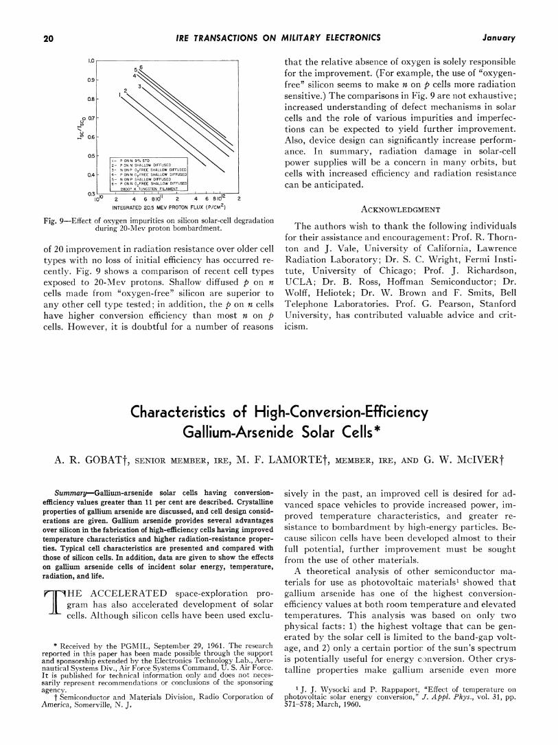
Fig. 9-Effect of oxygen impurities on silicon solar-cell degradation T a wtoduring 20-Mev proton bombardment. The authors wish to thank the following individuals
for their assistance and encouragement: Prof. R. Thorn-of 20 improvement in radiation resistance over older cell ton and J. Vale, University of California, Lawrencetypes with no loss of initial efficiency has occurred re- Radiation Laboratory; Dr. S. C. Wright, Fermi Insti-cently. Fig. 9 shows a comparison of recent cell types tute, University of Chicago; Prof. J. Richardson,exposed to 20-Mev protons. Shallow diffused p on n UCLA; Dr. B. Ross, Hoffman Semiconductor; Dr.cells made from "oxygen-free" silicon are superior to Wolff, Heliotek; Dr. W. Brown and F. Smits, Bellany other cell type tested; in addition, the p on n cells Telephone Laboratories. Prof. G. Pearson, Stanfordhave higher conversion efficiency than most n on p University, has contributed valuable advice and crit-cells. However, it is doubtful for a number of reasons icism.
Characteristics of High-Conversion-EfficiencyGallium-Arsenide Solar Cells*
A. R. GOBATt, SENIOR MEMBER, IRE, M. F. LAMORTEt, MEMBER, IRE, AND G. W. McIVERt
Summary-Gallium-arsenide solar cells having conversion- sively in the past, an improved cell is desired for ad-efficiency values greater than 11 per cent are described. Crystalline vanced space vehicles to provide increased power, im-properties of gallium arsenide are discussed, and cell design consid- temperature characteristics, and greater re-erations are given. Gallium arsenide provides several advantages provedover silicon in the fabrication of high-efficiency cells having improved sistance to bombardment by high-energy particles. Be-temperature characteristics and higher radiation-resistance proper- cause silicon cells have been developed almost to theirties. Typical cell characteristics are presented and compared with full potential, further improvement must be soughtthose of silicon cells. In addition, data are given to show the effects from the use of other materials.on gallium arsenide cells of incident solar energy, temperature, A theoretical analysis of other semiconductor ma-radiation, and life.
terials for use as photovoltaic materials1 showed thatr HE ACCELERATED space-exploration pro- gallium arsenide has one of the highest conversion-
gram has also accelerated development of solar efficiency values at both room temperature and elevatedcells. Although silicon cells have been used exclu- temperatures. This analysis was based on only two
physical facts: 1) the highest voltage that can be gen-erated by the solar cell is limited to the band-gap volt-
* Received by the PGMIL, September 29, 1961. The research age and 2) only a certain portior: of the sun's spectrumreported in this paper has been made possible through the supportand sponsorship extended by the Electronics Technology Lab., Aero- is potentially useful for energy c.;)nversion. Other crys-nautical Systems Div., Air Force Systems Command, U. S. Air Force. talline properties make gallium arsenide even moreIt iS published for technical information only and does not neces-sarily represent recommendations or conclusions of the sponsoringagency. ' J. J. XV;ysocki and P. Rappaport, "Effect of temperature on
t Semiconductor and Materials Division, Radio Corporation of photovoltaic solar energy conversion," J. Appi. Phys., vol. 31, pp.America, Somerville, N. J, 571-578; March, 1960.

1962 Gobat, et al.: Gallium-Arsenide Solar Cells 21
attractive as a solar-cell material, and superior to sili- materials having high carrier mobilities. Because ofcon, cadmium telluride, cadmium sulfide, or the graded- the high electron mobility in gallium arsenide with car-band-gap gallium-phosphide-gallium-arsenide mate- rier concentrations exceeding 1015/cm3 surface lossesrials. can be very low.3'5 Silicon cells, on the other hand, usu-
This paper describes the characteristics of gallium- ally have appreciable surface losses because of the higharsenide solar cells having conversion efficiencies greater surface-recombination velocity and the low carrier mo-than 11 per cent. The cells are fabricated from mono- bility in the highly doped surface. The characteristicscrystalline n-type material with an impurity concentra- of silicon cells may be influenced by the surface to ation of 1017 per cubic centimeter. Zinc diffusion is used greater extent than those of gallium-arsenide cells.in the construction of the junction to provide a penetra- The high photon-absorption coefficient of galliumtion of 1 to 3 microns, a surface concentration of 1020/ arsenide permits the fabrication of very thin cells. Be-cm3, and a sheet resistance ranging from 20 to 60 ohms cause the major fraction of photons which can createper square. The total resistance of the cell is less than 10 hole-electron pairs have absorption coefficients greaterohms resulting in a small internal power dissipation. If than 104/cm,3 95 per cent of the photons are absorbed ineither the contact resistance or the diffused-layer sheet a layer less than 3 microns thick. Silicon and cadmium-resistance is high, internal power dissipation appreciably sulfide cells must be made much thicker because of theirreduces conversion efficiency; the grid structure min- smaller absorption coefficients. Very thin cells fabri-imizes dissipation in the diffused layer. An antireflec- cated by epitaxial growth techniques should reduce bothtion coating on the top surface of the cell reduces re- cost and weight requirements, and thus have unques-flectance from 31 to 9 per cent. tionable advantages for space-vehicle applications.
Although the lifetime of electron-hole pairs is muchFEATURES OF GALLIUM ARSENIDE shorter in gallium arsenide than in silicon, the electron
Because gallium arsenide has a large band-gap value, mobility and hence also the electron-diffusion coefficientthe measured temperature-degradation coefficient of at a carrier concentration of 108llCM3 is nearly twoGaAs cells is approximately one half that of silicon cells. orders of magnitude greater than in silicon. The diffu-Gallium arsenide also has a potentially higher room-tem- sion length for electrons in gallium arsenide is approxi-perature efficiency value. Moreover, the larger masses mately 1 micron for a lifetime value between 10-10 andof the gallium and arsenic atoms result in a higher 10-9 sec and an impurity concentration of 1018/cm3.threshold energy under bombardment by high-energy Gallium arsenide also withstands a greater degree ofparticles. Lower lifetime values in gallium arsenide also radiation damage if recombination takes place throughgive higher radiation resistance under bombardment the medium of recombination centers because its crys-above the threshold energy. In addition, the higher car- talline perfection is poor prior to bombardment. If rec-rier mobilities of gallium arsenide2 provide a lower series ombination is radiative, on the other hand, the imper-resistance1 which reduces Internal power dissipation to a fections introduced below a certain concentration donegligible value,2 a greater minority-carrier diffusion not affect lifetime. It is only when the damage becomeslength for a given lifetime value, and reduced surface- very severe and a high concentration of recombinationrecombination losses.3 centers is introduced that recombination through theThe absorption coefficient for photons is higher in centers begins to reduce the lifetime to a value lower
gallium arsenide than in Filicon.3 The higher absorption than the radiative recombination value.coefficient makes it easier to design for a higher collec-tion efficiency. In high-efficiency gallium arsenide cells, CELL CHARACTERISTICSmore than 95 per cent of the photons are absorbed in Although gallium-arsenide solar cells are similar tothe diffused layer. The p-n junction is placed as close silicon cells in general construction details, their char-to the surface as possible without appreciable increase acteristics are quite different, as shown in Table I. Gal-in the sheet resistance. In silicon cells, however, almost lium-arsenide cells have a larger open-circuit voltage be-25 per cent of the photons are absorbed beyond the p-n cause of the larger band gap. Because a correspondinglyjunction in the base region. As a result, silicon cells must smaller portion of the solar spectrum is used, however,be designed with an optimum junction penetration so the short-circuit current density is smaller, the matchedthat minority carriers are collected from both sides of load resistance is higher, and the number of cells re-the junction. This type of design is more dificult be- quired in a series-parallel circuit design is different thancause the minority-carrier diffusion lengths cannot be for silicon cells. Typical voltage-current characteristicspredicted accurately prior to fabrication, of high-efiMciency gallium-arsenide cells are shown inAlthough a high absorption coefiMcient may produce Fig. 1.
excessively high surface losses through surface recoin- Conversion effciency for these cells is calculated onbinatin suracelsses an bereducd conideraly fo D. A. Jenny, J. J. Loferski and P. Rappaport, "Photovoltaic
effect in GaAs p-n junctions and solar energy conversion," Phys.2 D. A. Jenny, "The status of transistor research in compound Rev., vol. 101, pp. 1208-1209; February, 1956.semiconductors," PROC. IRE, vol. 46, pp. 959-968; June, 1958. 5M. F. Lamorte has obtained a solution of collection effciency
3D. A. Kleinman, "Considerations on the solar cell," Bell Sys. which includes surface-recombination velocity and the built-in fieldTech. J., vol. 40, pp. 85-115; January, 1961. established by the erfc impurity distribution.

22 IRE TRANSACTIONS ON MILITARY ELECTRONICS January
the basis of active area, i.e., total area minus grid-con- over the useful portion of the solar spectrum to antact area. The area of the stripes, however, is not more average value of nine per cent, and restores the short-than 5 per cent. Efficiency values for the gallium arse- circuit current density to 29 ma/cm2. If a collectionnide cells were greater than 11 per cent in all cases, and efficiency of 100 per cent is assumed, the coating mustin isolated cases reached as high as 13 per cent in normal have the following properties: an index of refraction ofsunlight. 1.8+0.2, and a zero-order thickness equal to a one-The open-circuit voltage for gallium-arsenide cells is quarter wavelength match, which is required to mini-
usually greater than 0.85 v, although values as high as mize reflectance in the wavelength range from 0.6 to0.96 v have been observed with an incident energy of 0.7 micron. The coating used is silicon monoxide, which100 milliwatts per square centimeter. The open-circuit has an index of refraction of approximately 1.8 whenvoltage of high-efficiency cells is within 0.05 v of the properly applied, and the calculated thickness isp-n junction built-in voltage, which is typically greater 925 + 175 A. Experimental data show an improvementthan 0.92 v. attributable to the coating as high as 22 per cent. Multi-
Values of short-circuit current density for gallium- ple coatings might be used to reduce the reflectance be-arsenide cells are more than one half the theoretical low 9 per cent, but it is questionable whether the in-values. The useful portion of the solar spectrum at sea creased cost would be economically feasible.level for gallium arsenide provides a current density of The rectangular shape of the voltage-current curves32 ma/cm2, provided the reflectance at the surface is in Fig. 1 indicates that the internal power dissipationzero.6 However, the reflectance at the gallium-arsenide attributed to the series resistance of gallium-arsenidesurface of approximately 31 per cent reduces the cur- cells is small, or even negligible. This dissipation, whichrent density theoretical value to 22 ma/cm2. A properly reduces conversion efficiency, may also determine to adeposited antireflection coating reduces the reflectance large extent the steps which must be taken to maintain
the temperature of the space vehicle to a manageableTABLE I level. The method used to determine internal power dis-
COMPARISON OF TYPiCAL DEVICE CHARACTERISTICS FORGALLIUM ARSENIDE AND SILICON HIGH-EFFICIENCY sipation is described briefly below.
SOLAR CELLS* The voltage-current relationship for a solar cell is
--|Si GaAs given by the following equation :'
Open-Circuit Voltage V,,, 0.6 0.9 volts J = J." - Jroet(V IR5) (1)Short-Circuit Current Density J,, 27 17 ma/cm2Matched Load Resistance RLmp 10 30 ohms where J IS the current density for a given voltage V, Jsc
is the short-circuit current density, and Jro is the space-* Incident solar energy is lOO mw/cm2; area of cell is 2 cm2. charge recombination current density, all in milli-
____ ____ ____ amperes per square centimeter.8 The term V in the ex-ponent is load voltage in volts, I is the load current in
____ /_ D milliamperes, and R, is the cell series resistance in ohms.The value of beta is given by
0.7 l ___ = qlAkT(volt-1). (2)
___ ____ ___ ____ The constant A is included to describe the nonideal di-ode behavior of the cell. The term Jro accounts for thedeviation from the saturation-current value. The value
>) 045 CXof A may be determined as follows:0
KT dInJ,,(30.3
where V,, is the open-circuit voltage in volts. If the- _ value of A calculated from (3) is substituted in (1) and
R. is set to zero, all the constants are known and theI.l - _ curve for zero internal power dissipation can be plotted.
12 ~~~Fig. 2 shows both theoretical and experimental curves
________. ___. for a typical gallium-arsenide solar cell for incident en-0 2 ~~MILLIAMPERES 1 14ergies of 100 and 880 mw/cm2. These curves show that
Fig. 1- Typical voltage-current energy-conversion characteristics tepwrdsiaini elgbefra nieteegfor high-eficiency gallium-arsenide solar cells (inlcident energy 7 WV. Pfann and WV. Van Rooshroock, "Radioactive anld photo-
is 100 mw/cm2). ~~~~~~~~electric p-n Junction power sources," J. Appi. Phys., vol. 25, pp.1422-1434; NAovember, 1954.
6 J. J. Loferski, "Theoretical considerations governing the choice 8 C-T. Sah, R. N. Noyce, and W. Shockley, "Carrier generationof the optimum semiconductor for photovoltaic solar energy con- and recombination in p-n junctions and p-n junction characteristics,"version," J. Appi. Phys., vol. 27, pp. 777-784; July, 1956. PROC. IRE, vol. 45, pp. 1228-1243; September, 1957.

1962 Gobat, et al.: Gallium-Arsenide Solar Cells 23
of 100 mw/cm2. The grid-structure contact of the cell for incident energies greater than those for which theis designed to provide maximum power output for grid structure is designed, and the power output shows aincident solar energies ranging from 100 to 140 mw/cm2, corresponding decrease. Efficiency at one value of inci-the latter value being equal to that encountered just dent energy is not necessarily a measure of efficiency atbeyond the earth's atmosphere.9 any other value. Solar cells designed for space applica-The optimum stripe separation for the grid-structure tions should be designed specifically for the range of en-
contact is given by the following equation: ergy values the vehicle is expected to encounter.
V0 1/2 Fig. 3 shows curves of efficiency as a function of inci-2c _= 2 _t 0 _ -2t (4) dent energy for gallium-arsenide solar cells using differ-
Eo + 2RL[Jsc -JroCVO(l- Eot)] ent grid structures. For cells C and D, which have stripe
where 2w is the stripe separation in centimeters, 2t is the separations of 0.67 cm, the efficiency decreases as thestripe thickness in centimeters, V0 is a constant voltage incident energy increases. For cells A anid B, which havemidway between stripes in volts, Eo is the electric field a stripe separation of 0.05 cm, the efficiency is higheston the cell surface in volts per centimeter, Rc is the conI- between 0.7 and 0.8 wv/cm .tact resistance in ohms, and L is the stripe length in If the short-circuit current densityJag beComeS suffi-centimeters. When the short-circuit current density Js ciently high, the open-circuit voltage VO attains aincreases with increasing incidenlt energy, the optimum saturation value which is called the junction built-instripe separation must be decreased to minimize power voltage Oo. In high-efficiency cells this voltage ap-dissipation in the diffused layer. As shown in the second proaches one volt, as shown in Table II. Values of 0.set of curves in Fig. 2, the power dissipation increases lower than 0.9 usually indicate that both the open-cir-
cuit voltage and the short-circuit current density arepoor, and usually result in poor efficiency values. It can
CELL C ----THEORETICALJ -EXPERIMENTAL be shown that for Voc to approach -o the excess-minor-____ t___C__ __ - lity-carrier concentration must be equal to the majority-
carrier concentration in both the p and n regions. Ma-08__ ____ INCDENT terials with high-absorption coefficients, such as gallium
0ENmEwRGY2 I arsenide, generate a higher excess-carrier concentration0.7___ ___ 1 { l Xand more nearly approach the junction built-in voltage0.7INCIDENT,' \INCIDREGNT 1\ l under normal values of illumination.ENERGY
0.6 <L100 mw/cm2 > The calculated values of Jro for these cells are orders ofmagnitude greater than the saturation-current density,
La5 I which is of the order of 10-11ma/cm2. The typical values0 shown in Table II indicate that a recombination com-0.4-
0.3- B
0.2 -
o 20D 40D 60D 80D 100 120 140 0 0 0.1 0.2 0.3 0.4 0.5 0.6 0.7 0.8 0.9MILLIAMPERES INCIDENT-ENERGY DENSITY- WATTS
Fig. 2 Comparison of experimental and theoretical energy-con-cmversion curves for galliulm-arsenide cells (zero resistance is as- Fig. 3-Conversion efficiency as a fulnction of incident energysumed for the theoretical curve), for two values of stripe separation.
TABLE I ITYPICAL VALUES OF CEI L PARAMETERS FOR HIGH-EFFICIENCY GALLIUM ARSENIDE SOLAR CELLS
Cell (per cent) (votlts) (macm') (ohms) (ma/cmJro) (volts)A 11.1 0.86 16.9 23 2.1 9.05X10⁻⁵ 0.935B 11.6 0.84 18.4 21 2.0 1.31X10⁻⁶ 0.93C 11.5 0.90 17.2 24 2.1 8.64X10⁻⁵ 0.94D 11.2 0.90 17.2 23 1.6 3.12X10⁻⁹ 0.94E 11.3 0.91 17.4 23
9F. S. Johnson, "The solar conlstant," J. ]lleteorology, vol. 11, pp.431-439; Decemher, 1954.

24 IRE TRANSACTIONS ON MILITARY ELECTRONICS January
ponent in the space-charge region contributes to the rocal temperature is normally linear, as shown in Fig. 6,forward current. The values of A deviate sufficiently and ranges from 2.9 to 3.94 a0K/cm2. The increase infrom unity to suggest that the large Jro values are caused current from zero to 200°C is approximately 15 perby a recombination phenomenon in the space-charge cent, which is considerably smaller than the decrease ofregion. The values of activation energy Ea were deter- open-circuit voltage. If the short-circuit current couldmined by measurement of the reverse junction current.8 be made to increase even more rapidly with increasingThe existence of a trapping level near the center of the temperature, the efficiency-temperature coefficientband leads to the conclusion that the space-charge re- could be reduced by an amount related to the currentcombination takes place through the medium of re- increment.combination centers rather than a radiative recombina-tion phenomenon. 1.C
TEMPERATURE CHARACTERISTICS X00.9 0.002 V/. I IAs stated previously, the temperature coefficient of o.o CELL D;
gallium-arsenide cells is approximately one half that of 0CELLE,
0.7silicon cells because of the larger band gap. This feature 0.7 m |0| [email protected] greater flexibility in the design of space-vehicle mQ 0.0021 V/@C
zequipment, and also eliminates the need for special pre- Xcautions required with silicon cells. Under certain condi- 05 -.tions it may be advantageous to use reflectors to in- 04 - - -crease the incident energy on the gallium-arsenide cells; 0 20 40 60 80 100 120 140 160 180 200because of the improved temperature coefficient, the TEMPERATURE-C
power output may increase appreciably. Fig. 4-Open-circuit voltage of four gallium-arsenidepoweroutput ma cells as a function of temperature.The degradation of conversion efficiency with increas-ing temperature results primarily from a decrease in 13open-circuit voltage. Fig. 4 shows the open-circuit volt-age of typical gallium arsenide cells as a function of tem- i12CEL2L ; -perature; the voltage-temperature coefficient for these - m03 / /Cfour cells ranges from 1.94 to 2.21 mv/°C. The open- 0 C;circuit voltage of the gallium arsenide cell at 2000C is 10 - M=- .0021 0l/0Cequal to that of the silicon cell at 25°C. The drop in AND 0.034 %/°Copen-circuit voltage of the gallium-arsenide cells from CELLS D'EEzero to 200°C is approximately 50 per cent. - -m=0.027%fc'lApproximately the same variation exists for conver- - - -
sion efficiency of gallium-arsenide cells, as shown in Fig. { - - N5. The temperature coefficient of conversion efficiency o - - - - - - -for the four cells ranges from 0.021 to 0.034 per cent/'C.The measured temperature coefficient of 0.025 per cent/ -20 40 6-D IC 1201-0 160 180 200'C is approximately one-half the measured value ob- TEMPERATURE-eCtained for commercially available silicon cells, which Fig. 5-Conversion efficiency of four gallium-arsenideranges between 0.04 and 0.06 per cent/0C. cells as a function of temperature.
In Fig. 5, two slopes are distinguishable for the curveof cell C, i.e., the temperature coefficient is lower below 23- --107°C than above this point. This change in slope has E, 22I |lbeen observed on several cells, although usually only CELL C;one slope is present. Where the change occurs, it is 21 m=3.87 AMP-K | ~~~~~~~~~~~~ 38
cm28attributed to the temperature variation of the short-cir- z 2C - - LCELL B;
cuit current of the cell. Although the short-circuit cur- m|2|9AMP-Krent of both gallium-arsenide and silicon cells usually i9 - -increases with increasing temperature, the increment is :§ { m 32<small compared to the decrease in open-circuit voltage. F11 Icl 1The break in the curve may be caused by a nonlinearity r--7 - - __ - ___ -in the current-temperature relationship. An increase in CE L \minority-carrier diffusion length due to the filling of o --|m39 AMm2'Ktraps and/or recombination centers and the decrease in ___ __ ___11 \the band gap at elevated temperatures could cause such 2o.413/T-*K3. 4
nonlinearity. ~~~~~~~~~~~~Fig.6-Short-circuit current density of four gallium-arsenideThe rate of change of short-circuit current with recip- cells as a function of the reciprocafl of temperature.

1962 Gobat, et af.: Gallium-Arsenide Solar Cells 25
SPECTRAL RESPONSE 100
Because the spectral distribution of artificial light 90differs significantly from that of the sun, evaluation ofcells in such light is not satisfactory. Discrepancies F 80often result when cells are evaluated both indoors be-neath an artificial light and outdoors in natural sun- 70light. These discrepancies occur because the conversion C1C Aefficiency is an integrated function of the spectral re- D60 ___ B
sponse characteristic, which may differ from cell to cellin both shape and magnitude. Although evaluation of 54 k
zsolar cells beneath a tungsten lamp or solar simulator is _standard practice, it should be emphasized that such ,,40p
wevaluation can serve only as a guide. In many respects,the collection efficiency determined from the spectral 30
w-Jdistribution of short-circuit current is a better measure 'Iof the cell efficiency. 20The collection efficienicy is the ratio of the number of
minority carriers separated by the p-n junction per unit '0time per unit wavelength to the photon flux per unit lwavelength.6 This ratio is influenced by the photon ab- o03 0.4 0.5 0.6 0.7 0.8 0.9sorption in the semiconductor material, the ratio of WAVELENGTH (0-104cmminority-carrier diffusion length to junction penetra- Fig. 7-Spectral response characteristics of gallium-tion, the surface-recombination velocity, and the built- arsenide cells.in drift field in the diffused layer. Some of these param-eters can be controlled by appropriate control of the combination losses. As a result, collection efficiency de-fabrication process. creases fairly rapidly at short wavelengths. New fabrica-
Because the drift field is negligible in the gallium tion techniques under investigation should increase thearsenide cells discussed in this paper, efforts were con- drift field substantially and provide a slower decreasecentrated on optimizing the other parameters for opti- in collection efficiency.mum design. Investigations are now under way to ob- The maximum collection efficiency occurs close to thetain a sufficiently high drift field to provide negligible edge of the bandwidth, where the absorption coefficientrecombination in the diffused layer. For the lifetime is approximately 104/cm. For this value, an appreciablevalues encountered in the diffused layer, the junction fraction of the hole-electron pairs are generated in thepenetration should be about 0.5 micron, with a surface junction region, where most are collected and separatedconcentration of 1020/cm3. by the junction built-in field. At shorter wavelengths,The use of the collection-efficiency ratio permits the the absorption coefficient approaches 105/cm; at this
calculation of the short-circuit current density under value, most of the hole-electron pairs are generated inany conditions of solar illumination. As a result, this the surface region.3 Some of the electrons recombine inratio may also serve as a relative measure of conversion the surface region and in the diffused layer, and a smallerefficiency. In addition, it can be used to determine sur- fraction of these carriers are collected by the junction.face losses.'0 It has been suggested, therefore, that the As a result, the collection efficiency is lower.collection-efficiency characteristic be specified for the Although some experiments have indicated that theseevaluation of solar cells. Unfortunately, this charac- losses in gallium arsenide may be reduced appreciably,4teristic is not easily measured because of the difficulty more recent work shows relatively high values." If theof calibrating the spectral light source. For the measure- usual light sources were employed in the latter work, thements given in this paper, a model No. 112 Perkin- rate of decrease of collection efficiency at short wave-Elmer spectrometer was used, and an Eppley thermo- lengths is even greater than that shown in Fig. 7. Thesepile in conjunction with a Liston Becker dc amplifier results indicate that the fabrication technique deter-was used to calibrate the spectral distribution of the mines the losses in the surface region and the diffusedphoton density of the spectrometer over the useful por- layer. In particular, the built-in drift field is important,tion of the spectrum. as are the surface-recombination velocity and the elec-
Typical collection-efficiency characteristics for four tron diffusion length.gallium arsenide cells are shown in Fig. 7. The drift field Fig. 7 shows a maximum possible increase in collec-in these cells is not sufficiently high to minimize both tion efficiency of approximately 60 per cent in the wave-recombination in the diffused layer and surface-re- length range from 0.4 to 0.8 micron. When this figure is
10 V. K. Subashiev, "Determination of recombination constants 11 D. Nasledov and B. V. Tsarenkov, "Spectral characteristics offrom spectral characteristic of a photoelement with a p-n junction," GaAs photocells," Soy. Phsys-Solid State, vol. 1, pp. 1346-1348;Soy. Phys.-Solid State, vol. 2, pp. 187-193; July, 1960. March, 1960.
26 IRE TRANSACTIONS ON MILITARY ELECTRONICS January
combined with the solar photon spectrum, it can be ex- cates that Jro and A may have changed to produce thepected that the short-circuit current density of a cell lower generated voltage.will show a maximum increment of approximately 50 The average degradation in efficiency was 56 per centper cent. This calculation results in the theoretical value after the cells were subjected to an average total flux ofof short-circuit current density. 7 X 10¹⁶/cm2. For silicon cells having com-parable con-
version efficiency (m of about 7 per cent), a 44-per centRADIATION-DAMAGE EFFECTS decrease fromi the injitial value resulted with a flux of
Tables III and IV show the results of electron and 3 X 101/cm2for n-oi-p cells and with an order-of-mnagini-proton bombardment on gallium-arsenide cells. Al- tude less flux for p-oni-n cells. These data show that thethough these results are preliminary, they suggest that radiation resistance of gallium-arsenide cells is approxi-gallium-arsenide cells have superior resistance to both mately twice that of n-on-p cells and 20 times that ofelectron and proton irradiation than silicon cells. p-on-n cells.
Both the current and voltage characteristics of the The gallium-arsenide cells were degraded slightly incells decrease after bombardment with electrons of the the mounting procedure; this fact is part of the reasoniorder of 0.8 M\4ev. However, the change in short-circuit for the discrepancy between the measurements outdoorscurrent is greater than the change in open-circuit volt- and those in artificial light. In general, high-efficienlcyage. These results suggest that a decrease in minority- gallium-arsenide and silicon cells degrade more easilycarrier diffusion length and/or an increase in surface than low-efficiency cells.losses occurred. A decrease in diffusion length is prob- Table IV shows the results of bomiibardment withably caused by a reduction in the lifetime value; an in- protons of the order of 19 Mev. In this case, the deg-crease in surface losses is probably caused by an incre- radation in open-circuit voltage is comparable to thement of surface-recomnbination velocity. degradation in short-circuit current. These data sug-
Unfortunately, the parameters Jro, A, and q, werenot measured prior to bombardment in these tests; - -
wtherefore, no reason can be given for the decrease inopen-circuit voltage Vo,. However, past experience indi- 7 - -0.
TABLE IIIRESULTS OF IRRADIATING GALLIUM ARSENIDE CELLS WITH 6.0 - -
z0.8 MEV ELECTRONS w
Initial _Conversion Degradation After Total Flux _ L KEfficiency ?7Tiotal (per cent) m 4.C -
(per cent) _w
Cell Arti- (elec- 30 CELL Lficial trons 1000 2000 3000 4000 5000 6000 7000 8000
Out- Sun /cm2) A77 /AJ.0 A V0 ARL TIME-HOURSdoors After X 1016
Mount- 77 ic V0Ui RL, Fig. 8-Life-test data for galliuim-arsenide cells operating intoing a 100-ohm load at 25°C.
E 6.6 6.9 58 50 13 74F - 4.8 4.3 54 42 10 58G 5.3 4.8 7.2 54 46 11 65H - 3.8 8.7 63 54 8 100 70CLI1 6.5 4.0 8.0 63 61 14 123- 1 6.0 nX \ } / E ~~~~~~~~~~~~~~~~~~~~CELL R
0.TABLE IV a ELL TRESULTS OF IRRADIATING GALLium ARSENIDE CELLS WITH
19 MEV PROTONS > 5.0 C£LL Qw
Initial
onversinc Degradation After Total Flux w EIL P
pEffiiencycTotal
lu _3__ _0_
Cell Arti- ~~~(pro-I
dor Moulnt- ?1i J80i V00i RT~ AIDR1.0RYNilg 0 § 000 2000 3000 4000 5000 6000 7000 8000
_ _ ~~~~~~~~~~~~~~TIME-HOURSX 7.5 5 .7 1 .2 48 43 25 30Y 7.4 6.0 1.2 50 |55 |31 |54 Fig. 9-Life-test data for gallium-arsenlide cells
-stored at elevated tem peratures.

1962 Egli: Progress in Thermoelectricity 27
gest that a decrease in diffusion length occurred, but to a polystyrene coating which was used as an anti-that there was also a substantial increase in space- reflection coating in the early development of the cells.charge recombination current. In addition, a change in Results to 7000 hours for the two groups are shown incarrier concentration may have reduced the value of /, Figs. 8 and 9.and contributed to the decrease in open-circuit voltage.The average cell degradation after proton bombard- CONCLUSIONS
ment was 49 per cent for a total flux of 1.2 X lOu3/cm2. Results on high-conversion-efficiency cells fabricatedThe resistance of gallium-arsenide cells to proton ir- from gallium-arsenide crystal substantiate earlier pre-radiation is from 10 to 20 times that of silicon cells hav- dictions that this material is highly suitable for solaring comparable efficiencies. As in the case of electron cells. Space-charge recombination current in gallium-bombardment, higher-efficiency cells degrade more arsenide cells is much larger than the calculated satura-rapidly. Again, some of the degradation resulted from tion current, as it is for a silicon junction. The grid-mounting the cells prior to bombardment; the actual structure contact should be designed for a given solar-degradation due to bombardment is probably less than energy ra,nge to reduce internal power dissipation. Gal-the values reported in the tables. lium-arsenide cells have improved temperature charac-
teristics as compared with silicon cells, and are more re-LIFE-TEST DATA sistant to electron and proton bombardment. Tempera-
Two groups of gallium-arsenide solar cells have been ture degradation always occurs in the open-circuit volt-life-tested to date. The first group operates into a age; radiation degradation occurs in the short-circuitmatched load, and is maintained at a temperature of current, and to a smaller degree in the open-circuit25°C. A tungsten lamp is employed to provide the inci- voltage.dent energy; the intensity is adjusted for an equivalent100 mw/cm2. The second group is stored in air or dry ACKNOWLEDGMENTnitrogen at temperatures between 100 and 180°C. The authors wish to express their appreciation to J.Although several of the cells have degraded badly, the Wysocki for valuable discussions on radiation bombard-
degradation for most units has not been greater than ment and for permission to publish the data shown in20 per cent. Some of this degradation may be attributed Tables III and IV.
Progress in Thermoelectricity*PAUL H. EGLIt
Summary-Of the several processes by which heat is directly INTRODUCTIONtransformed to useful electric power thermoelectricity offers uniqueadvantages for several areas of application. The absence of moving T HERMOELECTRICITY has been investigatedparts and the simplicity promise high reliability, silence, and long- intensively in the United States for about fivelived, maintenance-free operation both as a power source and as a years, and progress has been excellent. Importantheat pump for refrigeration and temperature control. A substantial applications are already assured. Nevertheless, it is stilleffort devoted to materials development has produced new semi- early in the research on this subject, too early to stateconductors with an integrated theoretical efficiency of about 20 per aan e howe far-reaching the aplcto willcent. Further progress in materials development is needed to achieve with assurance how far-reaching the applications willmajor goals in both military and commercial applications, but im- become. Work has hardly started on some importantportant uses can already be visualized. Small power plants for remote problems of thermoelectricity, particularly problems ofareas and auxiliary power supplies for space vehicles are awaiting f a e w h afabrication and engineering which have an importantengineering improvements, some of which again require improvedmaterials for use as electrical contacts and electrical and thermal bearing on the economics of thermoelectric devices.insulators. Similarly in refrigeration, important military applications Most of the effort has accordingly been directedand special commercial devices can be produced with existing toward military applications, particularly toward thethermoelectric materials when engineering problems and the auxil- several urgent needs for power sources which cannot beiary materials problems are solved,.e ycnetinleupet
* Reevdb. h G L coe ,91 The important military requirements for new powert U. S. Naval Research Laboratory, WAashington, D. C. sources can be classified inl four categories, each one of