Embed Size (px)
Citation preview
-r-::. .) \ ' , '\-:-..' t . "'\ J- >'
,
Chapter 5
Sigma-delta Modulator Design
Tool
5.1 Motivation
Tn
A multi-standard design often involves extensive system level analysis and ar
chitectural partitioning, typically requiring extensive calculations. To expedite
the handling of complicated design calculat.ious, a Graphical User Interface (GUI)
based design tool is described in this chapter. In particular, multi-standard sigma
delta modulator design for three wireless communication standards consisting of
GS:-!, WCDMA and WLA:"l is focussed. A 2-2-2 reconfigurablc sigma-delta mod
ulator is proposed which can meet the design specifications of the three standards.
A low-distortion swing suppression sigrua-deh.a modulator (SDM) has been cho
sen which is less sensitive to circuit imperfect.ions. especially at very low ovcrsain
piing ratios, Further. the toolbox incorporates all the significant non-idealities
which affect the pcrfonu.un« of a sigma-ddtCl modul.itor. TIl<" signH1-,kltc\ mod
ulator design tool is cleveloped using the Graphical User Interface Development
Environment (GUIDE) in l\latlabTA1
99
5 .2 Int r od uc t ion
5.2 Int roduction
The rapid evolut ion of digital integrated circuit technologies and <ill {'WI' ex
pand ing growt h of wireless communicat ions have motivated the de velopment of
highly integrated multi -standard receivers . Xew architectures and circuit tech
niqu es need to lit' explored in the design of fully integrated. multi-st andard RF
transceivers (3) . (39). T hus reccnfigurahility is a major focus of recent RF
transceiver IC designs which has LWIl 11.'.;('(1 to increa..e Loth the integration and
adaptability to multiple RF commnnicarion standards . The main challenge here
i-, to design low-power, high dynamic range. compac t multi -mode (89) ana log to
digita l converters which r-an meet the resolution a nd bandwidth reqniremonts of
different communication standards . Our choice is flo sigm a-d elt a ADC bec ause of
its great features for adaptability and programmability.
- ', ,._.-...- .
._ ,._._- -_..- - ..~... ).- ,.,
...-
----_.-~-'-'-,_.......--'-_...-._.
,
'" -
•!•
_ " ..__ _--,- ......•--..
.
-+-
_.
Figure 0.1: GU I for Xlulti-standard Sigma-Delt a Modulat or Design Toolbox
!OO
5.3 Sigma-delta Modulator Design Toolbox
5.3 Sigma-delta Modulator Design Toolbox
The toolbox is developed using Matlab" Simulink models and the front-end GUI
is developed using GUIDE. With this toolbox, the user can select the required
wireless communication standard and obtain the corresponding multistage sigma
delta implementation. The toolbox will help the user or designer to develop
the sigma-delta modulator for multiple standards without requiring a complete
understanding of the underlying methods. Thus it provides a powerful tool for
the design engineer to perform a quick design and aualysis.
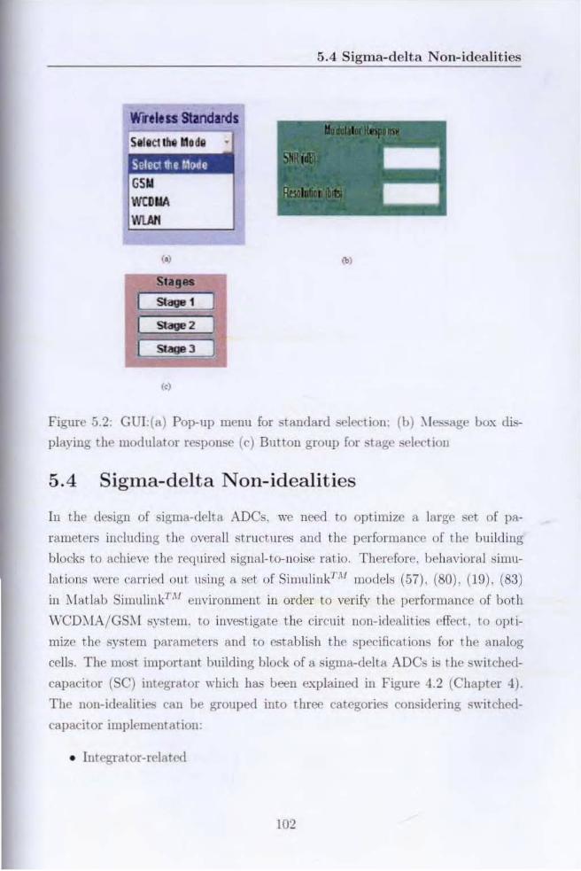
The front panel of the GUlis shown in Figure 5.1. Initially, the desired
standard is selected from the pop-up menu as in Figure 5.2a and the modulator
is designed by pressing the push button named Start Simulation. The modulator
details such as the order. bandwidt.h for a selected standard. oversampling ratio.
sampling frequency and its corresponding sampling period. input signal frequency.
required dynamic range ami tllf' number of quantizer bits are displayed on the
GUI as in Figure 5.4. The modulator response, signal-to-noise ratio (SNR) in dB
and the number of resolution in bits are displayed uliing the message box shown in
Figure 5.2b. Stages is a button group that holds a group of three buttons tagged
as Stage 1. Stage 2, and Stage 3 shown in Figurc 5.2c. The desired response. of
the individual stages. cascaded responses after each stage or the multistage overall
response, can be displayed in the Arcs window by pressing each stage button.
The push button named Histogram Plot is used to display the histogram of the
integrator outputs as shown in Figure 5.3. The power spectral density (PSD)
plot for the selected standard \VLA"I is displayed in Figure 5.4 using the A.U8
in the GUI. The Close is a push button which closes the GUI window, once it is
pressed.
The simulations were performed by incorporating most of the significant sigma
delta non-idealities in the toolbox. The main non-idealities considered here arc
finite and non-linear de gain. slew rate and gain-bandwidth limitations, amplifier
saturation voltage, capacitor mismatch. opamp input referred noise, kTIC noise.
clock jitter and DAC capacitor mismatch.
101
5 .4 Sigma-delta N on- id ea lit ies
W"relu s Standards
GSNwrONAW1.AIt
'oj~S"t''''g'''''''''''''''
St_l
St_2
("
0>,
Figure 5.2: G UI:(a ) Pop-up menu for standard selec t ion : (h) ~It ,:, :,ag(' hex db
playing the modulator response (e) Button group for stage selection
5.4 Sigma-delta Non-idealities
In thc design of sigma-delta AOCs, we need to opt.i mize a large sot of pa
ramct ers including the overal l s t ructures an d the performam-e of t ill' bu ildi ng
blocks to achieve t he req uired signal-to- uoiso ra t io. Therefore. beh avio ra l simu
lat ions \ \1.' 1'(' ca rried ou t using H sl't of SinmlillkT .\1 models (57). (SO). (19). (8:3)
ill }' lH t lah Silllu!inkT.\f environment in order to verify t he performance of horh
\ r CO:\IA/ GS:\1 sys tem. to inves ti gat e the circuit non-idcalitics vffect. to op ti
mize tho J'i)':;tPII1 para met ers and to establ ish the sp cr-ifir-ations for t he analog
cells. TI l<' most important building block of a sigma- delta AOC~ is t he switched
ca paci tor (SC) integrator which has been exp lained ill Figure 4.2 (Chapter 4).
The non-idealit ies can be grou ped into three ca tegories considering switched
capacitor imple ment ar ion :
102
5 .4 Sigma-delta N o n- Idea lities
...._-- '..---
"
..,.
•_ M..
J ~ ·)?kl• • , U.' • " U .'_ M
Figure 5.3: Histogram plot of the integra tor out puts
• Circuit related nou- idealiries
• Feed back DAC-rdatf"d
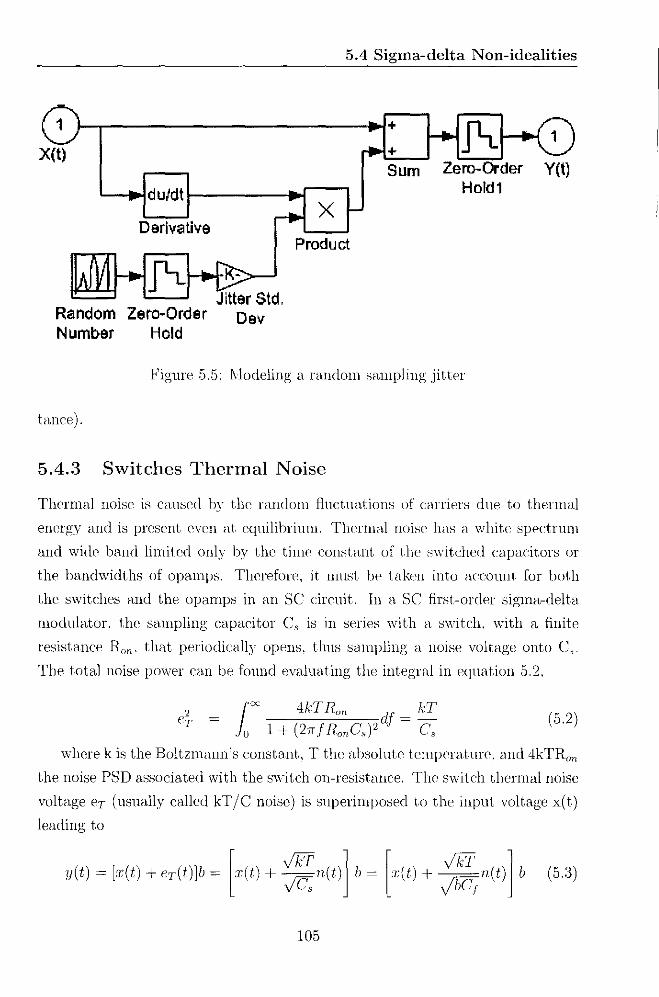
5.4.1 C lock J itter
Swit ched ca paci tor sigma-del ta mod ula tor is a sampled-dat a sys tem , where t he
variatious uf ti ll' d ock period have no direct effect OIL the circuit. performance .
cur-e t he signal has been sampled. T hus it is independent of t he st ructure or
order of t he mod ulator. Samp ling d ock j itt er results in uon-uuifonn sampling
a nd increases t ill' to tnl error power in the qu a ntizer output. T Ill' magnit ude of
t his f'ITOr is H funct ion of bo th the staristica l propr-rth-s of t he j itter and t he
input signal to the converter. The error int roduced when a sinusoida l signa l wit h
amplit ude A an d frequency fin is sa mpled at an instant which is i ll error by a n
amou nt 6 is given b.... equation 5.1.
. f. . d () ).r (t + <I) - J·(I) '" 2;r 00 004 eus (2;r fool ) = °dl r I (5. 1
T his effect can lIP simu lated with Simu link/-" b.... usin g the model (80) ShO\\11
in Figure' 5 .5. which implements eqnation 5. 1. Here we assumed that the sam-
103

5.4 S fgma-delt a Non-idealit ies
, - ': I!I
_.-..'..-----••
--?,:,~,~,;-
•,
_ ... _ I f'
----........--..-.-.-,....."--_._.....Dr__fOIIl
---
F igure fl.... : Display of the PSD plot of t he selected standard WLA:'\'
pliug uucertaiuitv 6 is a Gall:-.....ian random pW('t':--.... with standard deviatiou ~T,
\\·h..ther oversampling is helpful ill reducing t he j itter de-pend..;, on the nature of
the jitter. Since we a..;;'SUllU'" till' j itter white, the resul tant error has un iform power
spect ra l density from 0 to f. / 2, with a tot al power of ( 27ff",~T.4. rz/2,
5 .4 .2 In t eg rator N oise
Til l' 1I10st import ant ll (Ji ~ t' SOli n T'S affecting t ilt' opr-ra tion of all SC sigma-delta
modulat or are t he thermal noise associated to t ill' sampli ng switches and t i l! '
int rinsic nou...f' of the oper ational amplifier (i l), (Hi). TIll' total noise power of
the circuit is t he sum of till' t hcoret icalloop quantization noise power. the switch
noise power a nd the opamp noise power. Bf'('(H1~ of the large low frequeucv
gain of th e first integrator. the noise performance of a sigma-delta modulator is
determined main ly by t ill' switch a nd opamp noise of the input stage.
The-e effects can be simulated with Simuliuk1".\l using t he model (.sO) of a
nuisv integrator shown ill Figure 5.6. where the roefficicnt b represents t he in
regra tor ga in which is equal tu C.le! [sa mpli ng cnpacir anceyintegration capaci-
104
5.4 Sigma-delta Non-idealities
X(t)
f-......--------------~+
+Sum
'--l...duldt~---..,..--,xDerivative
~1Zero-Order y(t)
Hold1
Random Zero-OrderNumber Hold
Jitter Std,oev
Product
(5.2)
Figure 5.5: l\lodeling a random of\lnpJing jitter
tanee).
5.4.3 Switches Thermal Noise
Thermal noise is caused by the random fluctuations of carriers clue to thermal
energy and is present even at equilibrium. Thermal noise has a whito spectrum
and wide band limited only by the time constant of the switched capacitors or
the bandwidths of opamps. Therefore, it must be taken into account for both
the switches and the opamps in an SC circuit. In a se first-order sigma-delta
modulator. tho sampling capacitor C., is in series with a switch, with a finite
resistance Rm' that periodically opens, thus sampling a noise voltage onto C.,.
The total noise power can be found evaluating the integral in equation 5.2,
2 j'X 4kTRon d'f __ kTCT =
. 0 1 + (27rt RooC,)2 C,
where k is the Boltzmann's constant, T the absolute temperature, and4kTRon
the noise PSD associated with the switch on-resistance. The switch thermal noise
voltage eT (usually called kTIe noise) is superimposed to the input voltage x(t)
leading to
r vPf] r vPf 1y(t) = [x(t) + eT(t)]b = x(t) + 17" n(t) b =1:(t) + I17":n(t) b-rc, VbCf
105
(5.3)

5.4 Sigma-delta Non-idealities
1 kTIC 1/(z-1)X(t) I Y(t)kTIC Noise I Integrator',
II
,,b OpNoise
I ,I \
I ,Gain I ,
Op-Amp Noise. ,;, .. , , , , , , , , , , , , . , , , , , ., , ,
Figure 5.6: Model of a 'noisy int.cgrut.or
where n(t) denotes a Gaussian random process wit.h unity standard deviation.
while b is the integrator gain. Equation 5.3 is implemented hy the model shown
in Fignre 5.7.
1 f(uj2 ..
Xx(t) ..
Gain kTIC noise Sum Product2 y(t)
p X
Random Zero'()rder Product
Number Hold
Figure 5.7: Modeling switches thermal noise (kTIe) block
Since the noise is aliased in the band from 0 to 1',/2, its final spectrum is white
with a spectral density
S(f) = 2kT1f.,C, (5.4)
106
5.5 Integrator Non-Idealities
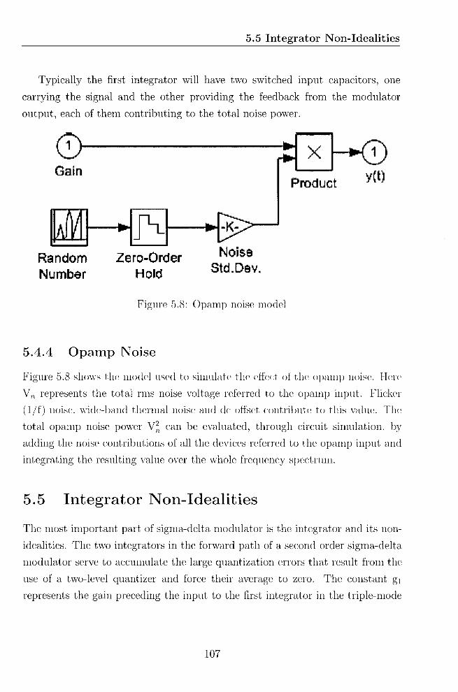
Typically the first integrator will have two switched input capacitors, one
carrying the signal and the other providing the feedback from the modulator
output, each of them contributing to the total noise power.
1
Gain
RandomNumber
Zero-OrderHold
NoiseStd.Dev.
xProduct
1
y(t)
Figure 5.8: Opamp noise model
5.4.4 Opamp Noise
Figure 5.8 shows thr: model used to suuulat« the dIed of t.h« opanrp noise. Hor«
Vn represents the total nus noise voltage referred to the opamp input. Flicker
(l/f) noi-«. wide-band t.hcnual noi«: awl de ofIset. «ontribut, to rhis valuo. Tit"
total opamp noise power V;' can be evaluated, through circuit simulation, by
adding the noise contributions of all the devices referred to the opamp input and
integrating the resulting value over the whole frequency spectrum.
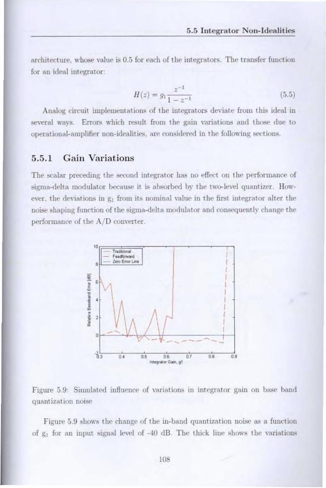
5.5 Integrator Non-Idealities
The most important part of sigma-delta modulator is the integrator and its non
idealities. The two integrators in the forward path of a second order sigma-delta
modulator serve to accumulate the large quantization errors that result from the
use of a two-level quantizer and force their average to zero. The constant g,
represents the gain preceding the input to the first integrator in the triple-mode
107
5.5 Int eg ra to r- N on- Id ealit ies
arc hitec ture. whose value is 0.5 for each of the int egrat ors. The transfer funct ion
for a n idea l integrator:
, - I
H(=) = YI ' 1 (0.5)1 - =-
Analog circuit imp lementat ions of the integrators dev iate from t his ideal in
severa l ways. Errors which resu lt from the gain varia t ions and those du e to
operationa l-ampl ifier non-ideali t ies . are considered in the following St>(..tions.
5.5.1 Gain Variat ions
T he sca lar preceding t he second integ ra tor has no effect 011 t he performance of
sigma-del ta modulator beca use it i:-; abso rbed hy the two-level quantizcr. How
ever. the devia t ions in gr from it -, nominal value in t he firs t integrator alter t he
noise shaping funct ion of the sigma-delta modulator a nd consequently cha nge the
perfor mance of the AID converter.
0T..llIl>c~.1 ;- F.~..d, z..o Em>r Un. I
II
'rV II
• I
v. /I, t- II
-~I
0__ ..... ..- -----_..1v' -
" OS 06 07IN.".. G_. I'
08 09
Figure 5.9: Simulated influence of varia tions III integra tor gain 0 11 base band
quant izat ion noise
Figu re 5.9 show.... the change of t he in-ba nd quantization noise a~ a function
of gl for a ll input signal level of -.10 dlj . T he thick hue shows rhc variations
108
5.5 Integrator Non-Idealities
s + Ir.1/z 1
IN + 1JOut1
Sum Unit Delay Saturation
Figure 5.10: Ideal integrator
for a traditional sigma-delta modulator. whereas the dotted line stands for feed
forward topology. Gain variations of as much as 20'1() from the nominal value
(0.5) has minor impact on the performance of the traditional one. whereas the
feed forward has almost no impact on the variations of gr showing the insensitivity
of t.he feed forward topology to component variations as the integrators process
only the quantization noise. However, gains larger than 0.6 for traditional. causes
the signal amplitudes at the integrator outputs to increase rapidly and the system
l)(~(,()l1lC:-; llllstahlc at all o.ulv stag(\ \VhCrCHs for f<~cd forward t.his COlIWS into (~H'('ct
only after 0.8.
IN
MATLAB 1----+1.Function
•Sum
lIz
Unit Delay Saturation
1..- ---< alIa~------1
alIa
Figure 5.11: Real integrator
109

jHJ
- Tra,...._ fH.........-.:l
\\\
0982 0.984 0'Hi 0911I 099 0992 09901 0996 09913Inl'i'I IGrL..k l~' (.Ila)
a.-- ,!•1 ••: ,••~ ,~
Leak
Figure 5.12: Iutluence of int egrat or leak 0 11 baseband quantization noise
5 .6 Opera t io nal-Amplifie r Nou- Idealit .ies
.~-~----------,
5.6 Oporat. ional-Amplifier Non-Id ea lities
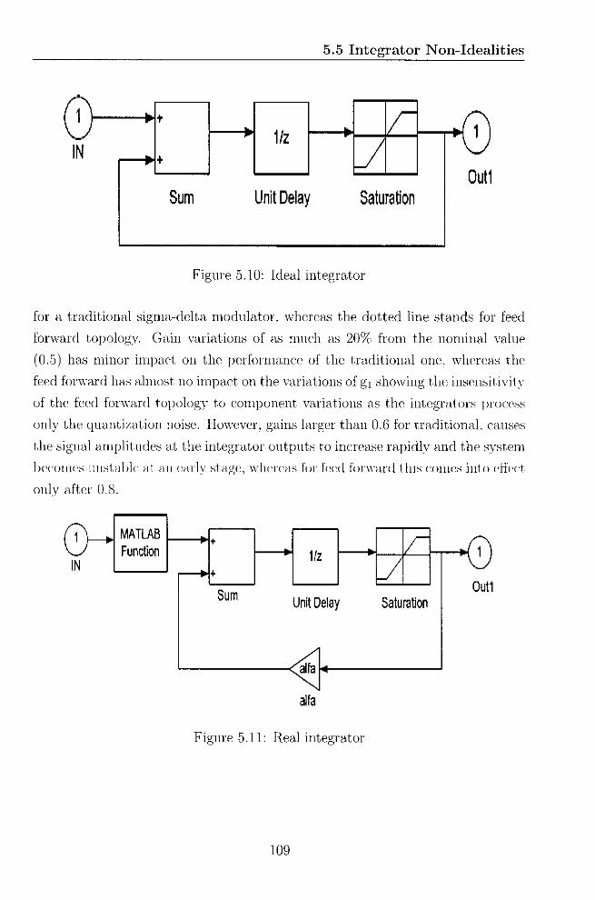
The beh avioural model of an ideal integra to r is given in Figure 5.10. One of
the major causes of performance degradation in SC sigma-delta modulators is
t he incomplete transfer of charge ill ti ll' SO integrators . T his non-ideal effec-t
IS a consequence of the operational amplifier non-idealit ics . ua melv tillite gain
and bandwidt h (8 \\" ). slew rate (SR) aud saturation voltages. The-e will he
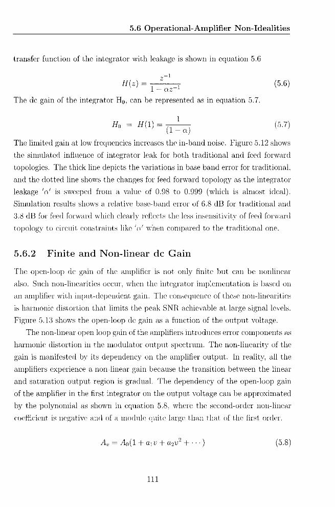
cons idered sep arately ill the following ser-tions . Figure 5.11 shows the mudd of
the real integrator including a ll I Ill' non- idealities.
T he idea l t ransfer Iunct ion of rhe int egrator assumes that its gain is infini te. a
chart..sctcristic impossible to obt ain in practice. However. t II(' act ual gai n is limit ed
by circui t const rainrs a nd in part icular "y t he operat iona! a mpl if ier open-loop gain
Ao. T he result is lo:-o.-;f int egration or known as int egrator leakage.. because only a
part of t he int egrator output 'nt of the previous period is added ttl t he IIt'W input
sample. Tho limited de gain of the int egra tor iI HTt'H_"f"S rhe in-hand noise. T he
5.6 .1
5.6 Operational-Amplifier Non-Idealities
transfer function of the integrator with leakage is shown in equation 5.6
Z-l
H(z) = 1 ~ ar 1 (5.6)
The de gain of the integrator Bo, can be represented as in equation 5.7.
IHo = H(I) = (1 ~ n) (5.7)
The limited gain at low frequencies increases the in-band noise. Figure 5.12 shows
the simulated influence of integrator leak for both traditional and feed forward
topologies. The thick line depicts the variations in base band error for traditional,
and the dotted line shows the changes for feed forward topology as the integrator
leakage '0' is sweeped from a value of 0.98 to 0.999 (which is almost ideal).
Simulation results shows a relative base-band error of 6.8 dB for traditional and
:3.8 dB for feed forward which clearly reflects 1.1)(; less insensit.ivity of feed forward
topology to circuit constraints like 'i,' when compared to the traditional one.
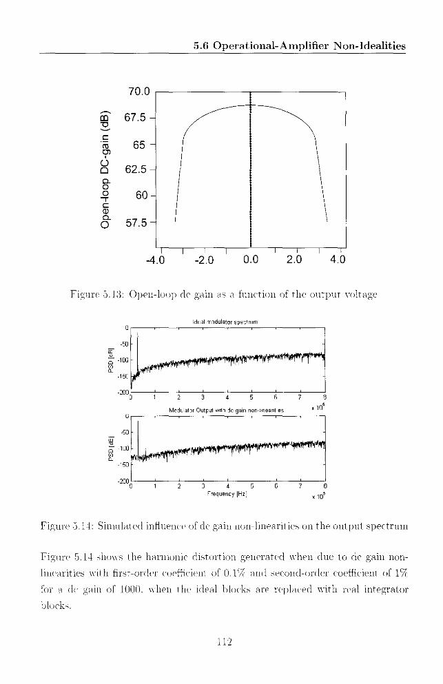
5.6.2 Finite and Non-linear de Gain
The open-loop de gain of the amplifier is not only finite but can be nonlinear
also. Such non-linearities occur, when the integrator implementation is based on
an amplifier with input-dependent gain. The consequence of these uon-Iincarit.ics
is harmonic distortion that limits the peak SNR achievable at large signallevcls.
Figure 5.13 shows the open-loop dc gain as a function of the output voltage.
The non-linear open loop gain of the amplifiers introduces error components as
harmonic distortion in the modulator output spectrum. The non-linearity of the
gain is manifested by its dependency on the amplifier output. In reality, all the
amplifiers experience a non-linear gain because the transition between the linear
and saturation output region is gradual. The dependency of the open-loop gain
of the amplifier in the first integrator on the output voltage can be approximated
by the polynomial as shown in equation 5.8, where the second-order non-linear
coefficient is nq;ative a!HI of a module 'illite large t.han that of the first order.
(5.8)
111
5.6 Operational-Amplifier Non-Idealities
70.0
CO 67.5 - I<:l~
cco 65 IOJ,o 62.5 -00.00 60 -...,cQl0. 57.5 -0
I I I I I I I
-4.0 -2.0 0.0 2.0 4.0
Figure 5.13: Open-loop de gain CiS (1 function of the output HlltHge
Ideal modulator spectrum
2 3 4 5Frequency [Hz]
6 7 8
l( 10~
Figure ,j. 14: Simulated infJuenrr of de gain nou-Iinearit.ics on the output spectrum
Figure 5.14 ,-.;lW\YS the harmonic distortion gencrated when due to de gain non
liur.uit ies wit h first-order coefficient of O.IS{ and second-order coefficient of IS{
for a ric gain of WOO. when t hc ideal blocks Me roplaced with real integrator
blocks.
112
5.6 Operational-Amplifier N Oll-Id ealit ies
55 ••
......
o
I .(101"
......
...
»>-r.........~. -_.
····r··
02
...rs
'"o
'"
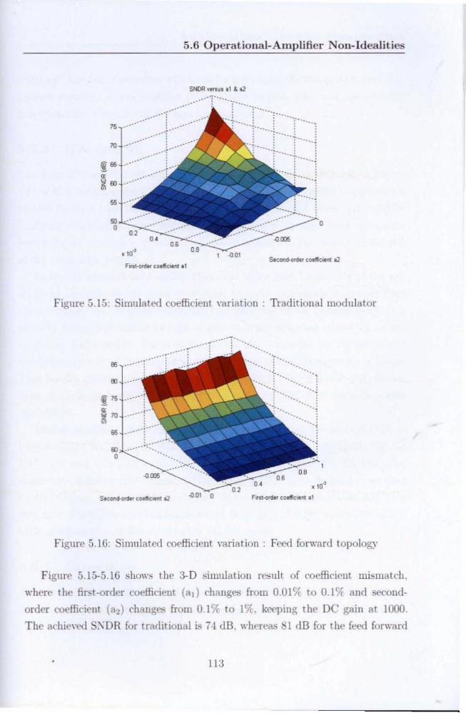
Figure 5.15: Simulated coefficient variation : Trad itional modulator
55
Ell •. •.
"OJ ••o
........~..,
.(101 0
.....: .....
"r' '.v-.,~ .. ..
..
.... ,.. ...~
.. .... ~
...
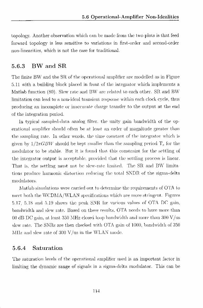
Figure 5.W: Simulated coefflcieut varia tion : F(-'('(I forward topology
Figure 5.15-5.16 shows t he 3-D simulatiou re-sult of coefficient misma teli.
where the first -order coefficient (ad changes from o.orx to 0.171: and second
order coefficient (a2 ) changes from D.I l)( to 19L keeping the DC gai n at 1000.
The achieved S:\DR for traditional is i -t dB. whereas 81 elD for t ilt' feed forward
5.6 Operational-Amplifier Non-Idealities
topology. Another observation which can be made from the two plots is that feed
forward topology is less sensitive to variations in first-order and second-order
non-linearities, which is not the case for traditional.
5.6.3 BW and SR
The finite BW and the SR of the operational amplifier are modelled as in Figure
5.11 with a building block placed in front of the integrator which implements a
Matlab function (80). Slew rate and BW are related to each other. SR and BvV
limitation can lead to a non-ideal transient response within each clock cycle. thus
producing an incomplete or inaccurate charge transfer to the output at the end
of the integration period.
In typical sampled-data analog filter. the unity gam bandwidth of the op
erational amplifier should often be at least an order of magnitude greater than
the sampling rate. In ot.her words. t.he time constant of tho integrat.or which is
given by 1127T{;llW should be kept smaller t.han the sampling period T, for t.he
modulator to be stable. But. it. is found that this constraint for the set.tling of
the integrator out.put is acceptnblc, provided that. the sett.liug process is linear.
That is. t.he settling must not. be slew-rate limited. The SR and B\V limit.a
tions produce harmonic dist.ortion n'd1H:ing the total SNDR of t.he sigma-delta
modulators.
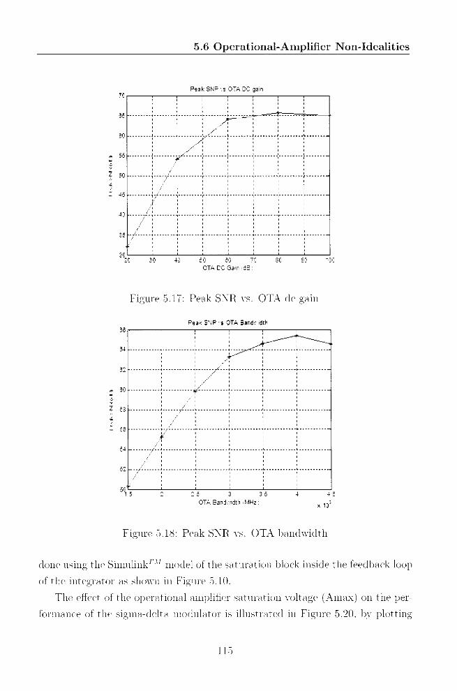
Mat.lab simulations were carried out. t.o detennine t.he requirements of OTA to
meet. bot.h the vVCDI\IA/vVLAN specifications which are more stringent, Figures
5.17, 5.18 and 5.19 shows t.he peak SNR for various values of OTA DC gain.
bandwidt.h and slew rate. Based on these results, OTA needs to have more than
50 dB DC gain. at least 350 :VIHz closed loop bandwidth and more than 300 V luoslew rate. The SNRs are then checked with OTA gain of lOOO, bandwidth of 350
MHz and slew rate of 300 V/us in t.he WLAN mode.
5.6.4 Saturation
The saturation levels of t.he operational amplifier used is an important factor in
limiting t.he dynamic range of signals in a sigma-delta modulator. This can be
114
5.6 Operational-Amplifier Non-Idealities
Peak SNP .s OTA DC gain7Dr--~-~-~-~--~-~-~----,
05 -----.--:-----.--;---------,---------~-.--.--~--~-~--.:....~--~-,,-,,--,,--~--~--~~__+: /:"": -: : : ,
cO --------; --------~ ---- -,~_>~'l-:.- -----~ --_.. -··1"·······~·········~·······
55 ••• -.-- -i------ --f'/~- ---i- --_. ----;---------:- --------i-- -------: -------1 " "I .. I , I I , ,
50 ----- --- ~ --- --/- -~- --- -----~ --- -----~- ------- ~- --- --_••:._._•• _•• ~ •••••••. ,
45 •-_••••• ~ (i ~•.•...... ~. - - - -;. - - - -- - - ~- - - - - - - - -:- - - -- - - - - i -------" I I I I , I, , ,
" , ,-IQ - - - - - :/- ~- - - - - - - - ~- - - - - - - _.~ - - - - - - - -, - - _. - - - - ~- -- - - - - - -:-- -- - - - - - r - -- - - --
, , ,, ,.', 1 , , , , ,
3:5 -..'.- --- - ~ ------ --.- ----- -- -~ ----- ---: -- ------.- ----- --r:-------~. _. ----, " i '" ," ,
3D 50 eo 70OTA CC Gain Id6'
30 90
Figure 5 17: PeRk S:\R vs OTA de: g8m
Peak SNP s OTA 6..nd':,idlh
: --+-----, -+--~---- I ---_~
C4 ----- ------•. -. ------- - ->-- - - - • - - - - - i_~':"7""<:'":'- -:- -----------~ -----------/', I
0: - -:. -. --.-. ----:-----.-.?-/- -:-----------~- ------.----~ -----------, ,
00 .. ------ -- -: ---. - ------,~(: ------ ---: - -- ----- ---~-. ---- ----- -~ ---- --- ---
;;r---~--~---~--~--~--____..,
, ,53 - .. - - - - - .. - ~ - - - - -. ,/- - - -~ - - - - - - --.- - ~ -. - - - - - - - - - -:-- - - - - - - - - - -~ - - - - - - - - - --
" ,, ,, ,55 ----------- •. ------- ----,••• -•••••••••••••••••••••••••• -••• - ••••• --------
. ' ,,/ , I , I ,
5-1 ---. - -- -,i- - ~ - - - - - - - - -. - -~ - - -. - - - - - -. ~ - - - - - - - - - -. -:- - - - - - - -. - - - ~ - - - -. - - - - --
, '", ", "5: _._/ ~ . ~ . __ J __ ••••••••••:•••••••••••• ~ •••••••••••
,:: 5 3 3 5
OTA 8 andoidth IMHz4
Figure s.is. Peak sxn \"S. OTA baudwidr h
done usiut; t h,' Suuuliuk"" ruoclel of the Sil t ura t ion block inside the feedb8ck loop
of the integrator <-1:-; shown ill Figur« 5.10.
The effect of the operational amplifier sar urat iou voltage (Atuax] on the per
Iorrnauce of the sigma-ddt" mociularor is illust ratecl in Figure 5.20. bv plotting
11-)

5.6 Operational-Amplifier Non-Idealities
Peal<: SNP 'S OTA 3Ie-:; Pale
:-4_~7
, ;~.----~':
60 -- ----; ---- ---:- ----_. ~ -------:-- -~;_.P-::; ------~- ------~ -_•••• ~•••••••~ ••••• _
'~.;/ :::55 ' , '/ I I , , , ,-. --";-- :" ;;:-_ :" :- _. ---~- ------;------~- ------~ -----
, /, I '" I
: ;¥:, : ::50 •••••• ~ •••••• ";"/ •••• ~ •••• _. -;-- - - - - -; - - - - - - ~- - - - -- - ~ - - - - - - ~- - - - - - -~ - - - - --
, " . "I /' , • I , , , ,
45 ._. _.- ~ -- /': --:---- ---i-------:- ---_. -; ------ -:- --_. --f-------:. -.. -..! -I :f I I , • I I , I
, '" ", " • iI iI' ,
-10 ---- ~.'_;- -----t-------t------~- ------l- - -••• ~ ••••••• ~ •••••• ~ •••••••:.-_.--
4343 :3112''-, f.3t12 " us
, , , , I
35 ,•••••• ~ ••••• - .:. - - - _. - ~ - -- - - - -:-- - - - -: - - - - - - ~- - - - - - - ~- - - - - - ~- - - - - - -~ - - - - --, " ,, " ,1 " •, ,
o
Feedtorward
-100 -50Input Level [db]
-+- Amex - 1 V ~l-s- Amax == 15 V ),---- ;--
;,
• :,-
,.~
20
o
60
40
80
-20-150
100
o-100 -50Input Level [db]
¥o ..... _.,: -.------,--
-20'---_---'--_~L-----..J-150
Traditional100
.~+- Amax = 1 V I~ Armu=15V
80 .... --------,-- tc .'
f ,
60 --- .... '~-I- ..."'.:
~;i
~~
'"40 - - - - ,- ~ - - u;
z t f zm m
20 -:-4---:--
Figure :).20: S'iTI as a fuuct ion of the input signal ampllr udc fur different values
of the operational amplifier saturation \-olta,!!;e (Amax)
the siniularcd S:\TI as a fiu.cr ion of the input SiglWI amplit ude fur different values
of Aiuax. For the tradit ioual 011f'. Cl sat urar ion \"(JltClge of .-\U1(-lX = 1.5 V with
a l'Cfen'll(,(' "Voltage of 1 V. does nut degt'Clde the pcrforur.mrr- siguific<111tly upto
llG
5.7 Circuit-related Non-idealities
a signal amplitude of -6dB, whereas a significant degradation occurs for a signal
amplitude of -16 dB when the saturation voltage Amax = 1 V due to the satu
ration of the operational amplifiers and not able to track the input signal. For
feed forward, this almost have no impact on the performance as the integrators
process only the quantization noise and the signal range is comparatively small.
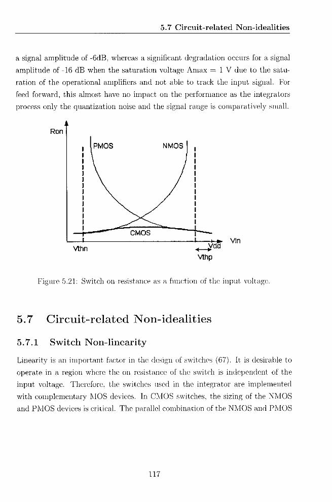
Ron
vthn
PMOS
CMOS
NMOS
Yin
Figure 5.21: Switch on-resistance as a function of t.he input voltage.
5.7 Circuit-related Non-idealities
5.7.1 Switch Non-linearity
Linearity is an important factor in the design of switches (67). It is desirable to
operate in a region where t.he on resistance of the switch is independent of the
input voltage. Therefore, the switches used in the int.egrator are implemented
with complementary ]'dOS devices. In C1\IOS switches. the sizing of t.he '1M OS
and PMOS devices is critical. The parallel combination of the N1\IOS and PMOS
117

5.7 C ircu it -related Non-idea lit ies
devi ces yie lds an effective resistance given by equation 5.9 .
[ (II') (II') lRos.cuos » IIXCw: T s( l(;.,x - lyHs )+ JlpCor T p ( l c SI' - IVTlIPI)
(5,9)
F igure 5.2 1 shows the swit ch on-resist ance as it function of input voltage.
T he input s igna l amplit ude. switch size a nd harmonic distortion sta t ist ics are
compiled to min imize the distortion introduced hy the swit ches . Figure 5 .22
shows t he sratistical resu lt of th e signa l to dist ortion ratio (SDH) '·S. switch size
with va r ious input signa l amplit udes. SDR call be iucrea..sed eit her by increasin g
the switch sizt' Of hy reducing the input signa l a mplit ude. Alt hough increasing
the switch can reduce th e harmonic dist ortion. it causes the para...itic capac itance
to increa se and rhus the clock feed- throu gh noise i... increased. T here is a trade off
between th e switch size and t he distort ions. It is found th at th e optimum value
of ,IH' switch size r-an be chosen as 30 IlIIl without much degradatio n ill SDH.
...... .
.'.• j,
" ," ,
.",.:
·f··..•... j ",
",: '.' ..: '.;
" ,". .. ' ..;
W.\. rJ Sl'Mch lum)
10o 0
02
> :"...... '
OJ
06
",.. '
70 ",
ID 60 ," .. '
a~ SO .. '..,;;; "
" ,
•ii JO .-,-",0~ ...., ...." ,
0020 ", ...-. -'. .. '
0 8 .....t.-:.. '
If1 put SIgn al I mplotud, (VJ
Figure 5.22: Di..tortion of th e sampli ng phase of a ll integrator
II "

5,7 C ircuit-relat ed Non-i dea li t ies
'1\ .
1 4 16 18 2F,.~y 1Hz] 110'
12 1 4 16 18 2Frequency (Hzl I 10'
0
"."
.... , ,, •'i' , ,
"
1r'".,
.5O
~ -100
~ -1g)
.zn
.,..,.o 0 2 0 4 06 0 8
(i1) IdRilI ModuliltDl'0
-5lJ
~ -100c .,5O'"c, ,.
-zn " 1 ' '[if.,..,.0 02 " O. DB "
Figure 5.23: Outp ut spectrum of the modulator with a nd wit ho ut m ismatch
5.7.2 Gain Mismatch
In casca ded modulators. ti lt' successive st ages serve to ran domise ti ll' qu anti zation
error. If lilt' caucellation of qna utiz nt ion error is com plete. the n the colorat ion in
the out put of the first stage is elimiuared. T he quantizuticu error of the final stage
approaches white noise. Unfortuuatelv, owing 10 gai n mismatch . quautizatiou
error from t he firs t stngo leak s into t hr-out put of the cascade , A major limi tat iou
of (" t";/'Hdf'd mod ula tors is the leakage of spect ral tones from the 1"/ stag!' into the
out put as H n-su lt of gain mis match. For exa mple. with a cumulativc tua tr-hing
error of 5%. t he following spectrum is obtained for a sinusoidal input of -li d B as
in Figure 5.2:l.
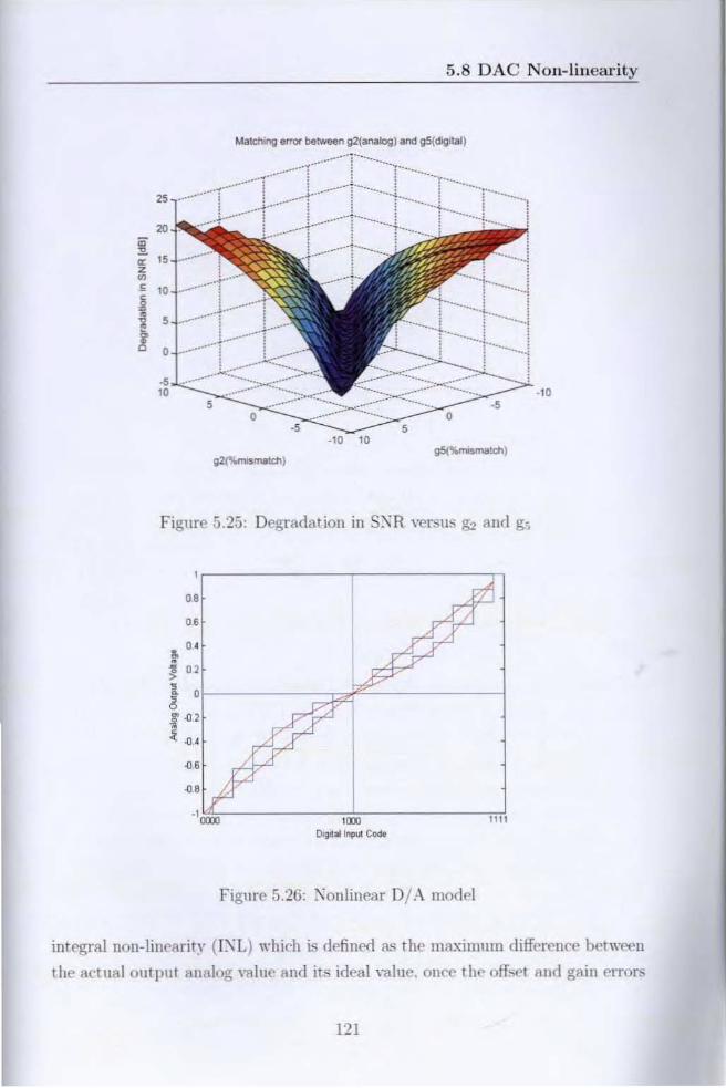
.\ Iat ch ing betwee n an alog (g \.g2) and digital (g,, ) gai ns is a ll important factor
wh ich ca n result i ll the qu a nti zation error fro m t he first stage no t fully ca ucellr-d.
Figures 5.2-1 and 5.25 depicts the sensit ivity of marchiug her ween an alog and
d igital gains 0 11 The performance of the modulat or. T he :J..D plot shows the
influence in signal- to- noise ratio as tho percentage of mismatch bet wee n t he analog
(gl'~l) and digital (gs) coefficients when t hcv an' varied from 0 to 1041£ . It is
119
5.8 DAC Non- linea r ity
-s..-.... -s
'ilS(~td'l)
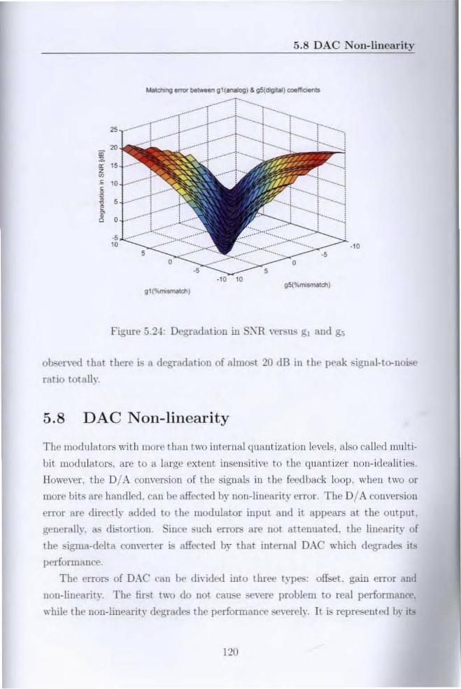
Figure 5.2-1 : Degr adation in S:'\R versus g, and go
observed that t here is a degradation of almost 20 IIIl in t he peak signal-to-noi....e
rat io totally.
5.8 DAC Non-linearity
TIl(' murlulat ors wit h more t hall two iuterua l quail! izat ion levels. also called multi
bit modulators, are to 11 large extent insensitive to tho quanti zer non-idealities.
However. the Oj A conversion of the signals ill t ho feedback loop. when two or
more bits are handled , can he atfcct r-d by non -Iinca ri tv er ror. The OJ A couversiou
error Me directly added to the modulator inpu t and it a ppears at the out put.
gener ally. a.... d istortion. Sinn' such errors are not attenuated. the linea rity of
t he sigma-delta converter is affected by that interna l O.-\C which degrades its
performance.
T ho errors of OAC call he d ivided into three types: offset. gain erro r and
non- linearity. T he first two do not cause sewn' problem to real performance.
while t he non-linearity degrades the performance s everclv. It i- repre-ented hy its
120
5.8 DA C Non-li nearity
s
"
.................'' ~..: :]...: :).~ r ·y , ~_..~.,• L..-~· · ·· ·~~~:r::·.:· ·.·. ·.·t., j.... i1_···'-" '-' - ,
- ~..~..li · ·..k_....~..-----.··' 1 "..-. .: -_...~ !
__.·····t···- ....j.._-.~_ ....!
:=:::t..~.._...:...:.•.•~.=.•.:.•.~.'.•.....-_•••..•.•::.•.•..._~.....- ....- ·.. ·1··.. --1- -. _.__~~:::;:_~;;.=~:'-<::~:~. · 10
---"
zs
200;a,
" "z00
s "§i e
l c
-s
"
Figure 5.2.5: Degradation in S;\,R y('[SUS ge and g'}
ce
"
1111,,'"Dlll'!aI Inpul Codo!
.,••
"t~ 02
l '1-- - - -;:;JP'fe:c..- - - -f".t .0 4
Figure ;'.26: Xonlinear DjA mod!'!
integral non-l inear ity (I\"L) which is defined a... t he maximum d itff' r! 'IH'f' between
the actual output analog \1'1111(' ami its ideal va lue . once thr- off~t't and ga in errors
121
5.8 DA C Non-linearity
..i.- - - __-
____~,-bC,~'!.. _
~_ ____ _ '..~l!J.Illl..~Roo __---.-.___Id!~ u.-..QSRzlQ.... _ _ _ _ __
'"0 1 0 2 03 O ~ OS 06 0 7 0 9 09
IN..[LS81
Figu re 5.27: SQ~R vs. I\'L for a -l th-order cascaded sigma-del ta mod ulator using
I-bit Oj A ill the first stage and -l-bit OJ.\. in the s econd stage.
have been corrected.
The nonlinear equariou relating the quant izer iupnt a nd output can be written
ill the form:
Y (t ) = .r( l) + a II (I ) + a,I'(1) + aJI' (I ) + ... (5.10)
Figure 5.26 shows the non-linear OJ.\. model which repres ents a t ransfer func
tion when ' the maximum I\'L is at t he maximum tlIHI minimum input values.
In t he following analysis. the imp art of non-linearity to SQ.:"J R of the OjA con
vertr -r is quantified as 1\' 1.. which is t he maximum deviation from the ide al Lbit
s tructures . When the SQ\' H with lion-linea r multi-hi t st ructure is worse them
the SQ\' H of the l -h it casf'. then it is obvious t hat extra circuit complexity and
power consum ptio n associated with the mult i-hit st ru cture ca nnot be motivated.
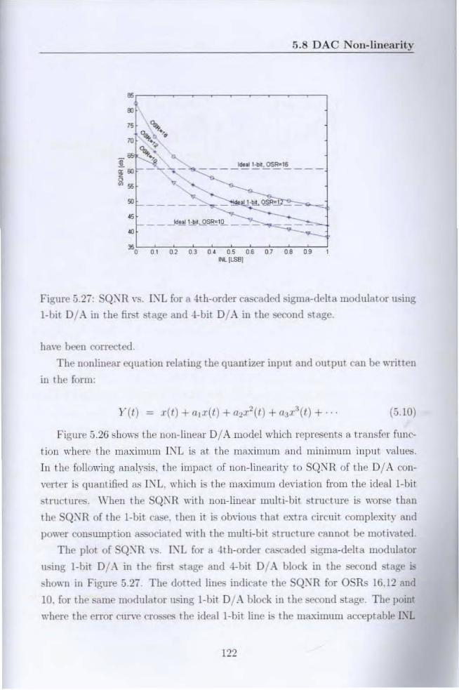
TI l(' plot of SQ~R \ 'S. I\'L for a -lth-order cascaded sigma-delta modulator
usin g l -bir OjA in the first stage and -l-hi t Oj A block in the seco nd stage is
shown i ll Figure 5.27. Til e dotted lines indicate the SQ\'R: for OS Rs 16.12 and
10. for the sa me modulator using l -bit Oj A block in the sec ond st age . T he point
where the erro r curve crosses the ideal l -bit line is the maximum accept able I);"L
122

5.n Performance Anal ysis
10'
Frequency [Hz]
10'Frequency [HzJ
o,----,----~---,
·1OO "-- - -'-;-- - -'
o,----,----~---,S~DR =836 1;1
·so ~ .III (2) :a 00 :~ . , .
· ' 50 ~ .
o [~OR . " 9d-so ~ .rg (1) i0 .100 ~. . .
l:' · ' OJ '''7 ..,.: .·1OO
10'Frequency 1Hz]
·1OO "--'-----'-;----'
Sr1DR =516 d-SO •••.••• .•• .•• ~. ••••••••
III (4) ,
~ ·100 '
c,
10'Frequency 1Hz}
.1OO"-- --'-;----'
Figure 5.28: PS D of (1) tilt' ideal modu lator; (2) with sa mpling ji tt er . T= 4 ns;
(3) wit h kTIC no ise. Cs = 1.25 pF; (4) with SR = 50 V I ps
for each case. T he acceptable IXL for OSHf' of 16.12 and 10 arc 0.:1 LSD. 0.55 LSB
and 0.7 LSB respectively. The IAL error in form of LSBs indicate that higher
error is tolerab le for lower OSH compared to the ),'1 = 1. '\;:1 = 1 converter. LSB
refers to the voltage difference between the adj acent code steps.
5 .9 P erformance Analysis
Behaviora l simulations were performed using t he Mat lab SimlllinkT.If mod els (80)
which includes t he various non- idea lities affecti ng the opera t ion of a SC sigma
delta mod ulator on a 211d-01"<1pr feed forward modu lator. Hen' on ly t he non
ideali t ies of the first integrator were considered. since thei r effects are not attenu
ated by noise shaping. Figure 5.28 compares the power spectral densit ies (PS D)
at t he output of the modu lator. when two of t he most sig nificant non-idealit ies in
t he first integrator are take n into RCCOllUL with t he PSD of t hv ideal modulator.
T ile spect ra put in evidence how the sampling jitter and kT IC noise increases the
123
5.10 Chapter Summary
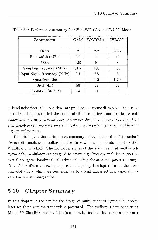
Table 5.1: Performance summary for GS~I, WCD~IA and WLAN Mode
Parameters GSM WCDMA WLAN
Order 2 2-2 2-2-2
Bandwidth (MHz) 0.2 5 10
OSR 128 16 8
Sampling frequency (MHz) 51.2 160 160
Input Signal frequency (MHz) 0.1 2.5 5
Quantizer Bits 1 1-2 1-2-4
SNR (dB) 86 72 62
Resolution (in bits) 14 11 10
in-band noise floor, while tho slew-rate produces harmonic dist.ortion. It must Ill'
noted from the results that the non-ideal eJf"do rcsultiun from pr.ui.i.:»! rirruit
limitations add up and contribute to increase the in-band noise-plus-dist.ortion
and. therefore can become a severe limitation to the perfonnauce achievable: from
a given architecture,
Table 5.1 gives the performance summary of the designed multistandard
sigma-delta modulator toolbox for the three wireless standards namely GSj\l,
WCDMA and WLAC\!. The individual stages of the 2-2-2 cascaded multi-mode
sigma delta modulator are designed to attain high linearity with low distortion
over the targeted bandwidth, thereby minimizing the area and power consump
tion. A low-distortion swing suppression topology is adopted for all the three
cascaded stagos which arc less sensitive to circuit imperfections, especially at
very low oversanipliug ratios.
5.10 Chapter Summary
In this chapter. a toolbox for the design of multi-standard sigina-delt.a modu
lator for three wireless standards is presented. The toolbox is developed using
Matlab™ Simulink models. This is a powerful tool as the user can perform a
124

5.10 Chapter Summary
quick design and analysis without a thorough understanding of the underlying
methods. The toolbox incorporates most of the significant non-idealities like fi
nite and nonlinear dc gain, slew rate and gain-bandwidth limitations, amplifier
saturation voltage, capacitor mismatch, opamp input referred noise, kT IC noise,
clock jitter and DAC capacitor mismatch. Behavioral simulation results indi
cate that the Ieedforward topology is less sensitive to circuit imperfections when
compared to tho traditional topology. These simulations help us to examine the
trade-otb Ixtwrou the diftoront par.uuotcrs and ('hooS(' t.ho hest solution to fulfil
tho application requirements.
125


![Literature Review - INFLIBNETshodhganga.inflibnet.ac.in/bitstream/10603/8178/11/11_chapter 02.pdf · CHAPTER 2 Literature Review ... Lee and sheriff [11] ... refrigeration cycles](https://img.dokumen.tips/doc/110x75/5a9e414b7f8b9a21488dd6fb/literature-review-02pdfchapter-2-literature-review-lee-and-sheriff-11-.jpg)