Embed Size (px)
Citation preview
Chapter 4The ProcessorPart IPart I
Introduction
§4.1 Intro
� CPU performance factors� Instruction count
oduction
� Determined by ISA and compiler� CPI and Cycle time
� Determined by CPU hardware� Determined by CPU hardware
� We will examine two MIPS implementations� A simplified version� A more realistic pipelined version
� Simple subset, shows most aspectsM f l� Memory reference: lw, sw
� Arithmetic/logical: add, sub, and, or, slt� Control transfer: beq j
Chapter 4 — The Processor — 2
� Control transfer: beq, j

Instruction Execution� PC � instruction memory, fetch instruction� Register numbers � register file read registers� Register numbers � register file, read registers� Depending on instruction class
� Use ALU to calculate� Use ALU to calculate� Arithmetic result� Memory address for load/store� Branch target address
� Access data memory for load/store� PC � target address or PC + 4� PC � target address or PC + 4
Chapter 4 — The Processor — 3
CPU Overview
Chapter 4 — The Processor — 4

Multiplexers� Can’t just join
wires togetherwires together� Use multiplexers
Chapter 4 — The Processor — 5
Control
Chapter 4 — The Processor — 6
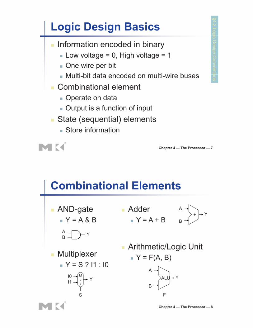
Logic Design Basics§4.2 Logic D
esign � Information encoded in binary
Low voltage = 0 High voltage = 1 Conventio
� Low voltage = 0, High voltage = 1� One wire per bit
Multi bit data encoded on multi wire buses ons� Multi-bit data encoded on multi-wire buses� Combinational element
� Operate on data� Output is a function of input
� State (sequential) elements� Store information
Chapter 4 — The Processor — 7
Combinational Elements
� AND-gate AY+
� Adder� Y = A & BA Y
BY+
� Y = A + B
B Y
Multiplexer� Arithmetic/Logic Unit
� Multiplexer� Y = S ? I1 : I0
A
� Y = F(A, B)
I0I1 Y
Mux B
YALU
Chapter 4 — The Processor — 8
S F

Sequential Elements� Register: stores data in a circuit
Uses a clock signal to determine when to� Uses a clock signal to determine when toupdate the stored value
� Edge-triggered: update when Clk changes� Edge-triggered: update when Clk changesfrom 0 to 1
D QClk
D
Clk
D
Q
Chapter 4 — The Processor — 9
Sequential Elements� Register with write control
Only updates on clock edge when write� Only updates on clock edge when writecontrol input is 1
� Used when stored value is required later� Used when stored value is required later
Clk
D Q Write
Clk
ClkWrite D
Q
Chapter 4 — The Processor — 10

Clocking Methodology� Combinational logic transforms data during
clock cyclesc oc cyc es� Between clock edges� Input from state elements, output to state p , p
element� Longest delay determines clock period
Chapter 4 — The Processor — 11
Building a Datapath
§4.3 Buil
� DatapathElements that process data and addresses
ding a Da
� Elements that process data and addressesin the CPU
� Registers, ALUs, mux’s, memories, …
tapath
� Registers, ALUs, mux s, memories, …
� We will build a MIPS datapathincrementallyincrementally� Refining the overview design
Chapter 4 — The Processor — 12

Instruction Fetch� Two state elements to store and access instructions
� Instruction memory� Instruction memory� Program counter (32 bits)
� An adder to compute the next instruction address� Add two 32-bit inputs� Place the sum on its output
Chapter 4 — The Processor — 13
Instruction FetchExercise: How are the components put together?
Chapter 4 — The Processor — 14

Instruction Fetch
32-bitregister
Increment by 4 for next instruction
register
Chapter 4 — The Processor — 15
R-Format Instructions� Read two register operands
Perform arithmetic/logical operation� Perform arithmetic/logical operation� Write register result
Chapter 4 — The Processor — 16

Load/Store Instructions� Read register operands� Calculate address using 16-bit offsetg
� Use ALU, but sign-extend offset� Load: Read memory and update register� Store: Write register value to memory
Chapter 4 — The Processor — 17
Branch Instructions� Read register operands
Compare operands� Compare operands� Use ALU, subtract and check Zero output
� Calculate target address� Sign-extend displacement� Shift left 2 places (word displacement)� Add to PC + 4
� Already calculated by instruction fetch
Chapter 4 — The Processor — 18

Branch InstructionsExercise: How are the components put together?
Chapter 4 — The Processor — 19
Branch Instructions
Justre routesre-routes
wires
Sign-bit wire
Chapter 4 — The Processor — 20
Sign bit wirereplicated

Composing the Elements� First-cut data path does an instruction in
one clock cycleone clock cycle� Each datapath element can only do one
function at a timefunction at a time� Hence, we need separate instruction and data
memoriesmemories� Use multiplexers where alternate data
sources are used for different instructionssources are used for different instructions
Chapter 4 — The Processor — 21
R-Type/Load/Store DatapathExercise: How are the components put together?
Chapter 4 — The Processor — 22

R-Type/Load/Store Datapath
Chapter 4 — The Processor — 23
Full Datapath
Chapter 4 — The Processor — 24

ALU Control§4.4 A S
i� ALU used for
Load/Store: F = add
mple Im
pl
� Load/Store: F = add� Branch: F = subtract
R type: F depends on funct field
lementatio
� R-type: F depends on funct field
on Schem
eALU control Function e
0000 AND0001 OR0010 add0110 subtract0111 set-on-less-than1100 NOR
Chapter 4 — The Processor — 25
1100 NOR
ALU Control� Assume 2-bit ALUOp derived from opcode
Combinational logic derives ALU control� Combinational logic derives ALU control
opcode ALUOp Operation funct ALU function ALU controllw 00 load word XXXXXX add 0010sw 00 store word XXXXXX add 0010beq 01 branch equal XXXXXX subtract 0110q qR-type 10 add 100000 add 0010
subtract 100010 subtract 0110AND 100100 AND 0000AND 100100 AND 0000OR 100101 OR 0001set-on-less-than 101010 set-on-less-than 0111
Chapter 4 — The Processor — 26

The Main Control Unit� Control signals derived from instruction
0 rs rt rd shamt funct31:26 5:025:21 20:16 15:11 10:6
R-type
35 or 43 rs rt address31:26 25:21 20:16 15:0
Load/Store
4 rs rt address31:26 25:21 20:16 15:0
Branch
opcode alwaysread
read,exceptf l d
write for R-type
d l d
sign-extendand add
Chapter 4 — The Processor — 27
for load and load
The Main Control Unit� Datapath with all necessary multiplexors and all control
lines identified
Chapter 4 — The Processor — 28

The Main Control Unit� The effect of each of the seven control signals
Chapter 4 — The Processor — 29
Datapath With Control
Chapter 4 — The Processor — 30

Datapath With Control� Setting of the control lines is completely determined by
the opcode fields of the instructionp
Chapter 4 — The Processor — 31
Datapath With Control� Setting of the control lines is completely determined by
the opcode fields of the instructionp
Chapter 4 — The Processor — 32

R-Type Instruction
Chapter 4 — The Processor — 33
R-Type Instruction
Chapter 4 — The Processor — 34

Load Instruction
Chapter 4 — The Processor — 35
Load Instruction
Chapter 4 — The Processor — 36

Branch-on-Equal Instruction
Chapter 4 — The Processor — 37
Branch-on-Equal Instruction
Chapter 4 — The Processor — 38

Finalizing Control� Truth table used to specify the control function for
the simple single-cycle implementationp g y p
Chapter 4 — The Processor — 39
Implementing Jumps
2 address31 26 25 0
Jump
� Jump uses word address
31:26 25:0
� Update PC with concatenation of� Top 4 bits of old PCp� 26-bit jump address� 00� 00
� Need an extra control signal decoded from opcode
Chapter 4 — The Processor — 40
opcode
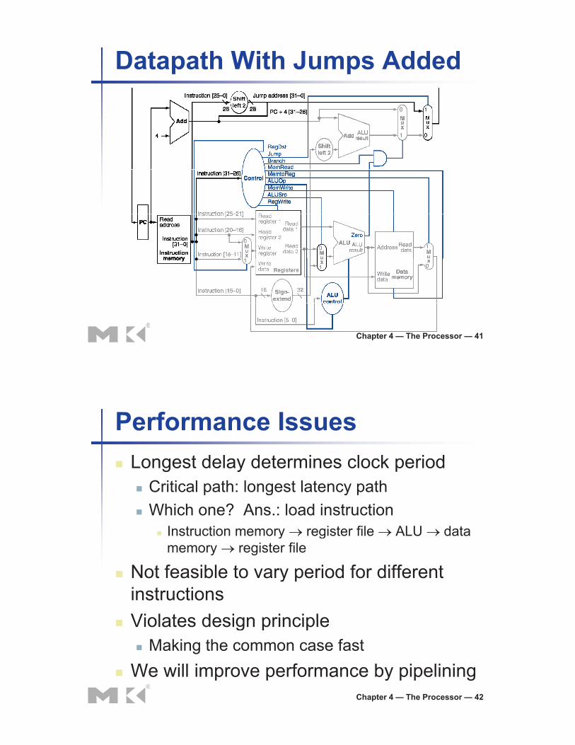
Datapath With Jumps Added
Chapter 4 — The Processor — 41
Performance Issues� Longest delay determines clock period
Critical path: longest latency path� Critical path: longest latency path� Which one? Ans.: load instruction
Instruction memory � register file � ALU � data� Instruction memory � register file � ALU � datamemory � register file
� Not feasible to vary period for different� Not feasible to vary period for differentinstructions
� Violates design principle� Violates design principle� Making the common case fast
W ill i f b i li iChapter 4 — The Processor — 42
� We will improve performance by pipelining