Embed Size (px)
Citation preview

95
CHAPTER 4
DESIGN OF DIGITAL DOWN CONVERTER AND
SAMPLE RATE CONVERTER FOR DIGITAL FRONT-
END OF SDR
4. 1 INTRODUCTION
Several mobile communication standards are currently in service
in various parts of the world and they do not interoperate with each other at
the physical layer. Since each wireless standard specifies a different channel
bandwidth, traditional single carrier techniques are no longer applicable
where the radio functions are optimized around a fixed channel bandwidth.
Moreover, the development cost of transmitters and receivers for these
standards remains high since as each standard requires a different radio
front-end (Mitola 1995). So, there is currently a strong interest in designing
a hardware platform that can support multiple standards simultaneously
resulting in what is called SDR.
SDR aims at replicating hardware functions in software running
on a generic platform. In doing so, the problems associated with hardware
implementations are solved. In addition the transmitter chains can easily be
changed to accommodate varying standards. So the idea of SDR requires
an expansion of digital signal processing towards the antenna. To achieve
the goal of catering to several channel bandwidths, the channel selection
process should be performed digitally as indicated in Scheuermann and
Gockler (1981) and Zangi and Koilpillai (1998). Such architecture is ideally
96
suited for a wireless base station that needs to process multiple channels
simultaneously. Thus at the base station, the multiple costly single–channel
radios are replaced with a single broadband radio. The rest of the channel
selection and filtering is performed digitally via DUC and DDC.
Thus the radio front-end captures a broadband signal (containing
multiple channels) rather than a single narrowband channel with better
dynamic range. Extending towards the signals of different standards that
might appear simultaneously at the receiver, the dynamic range can become
even larger. Thus there is a reduction in, the bandwidth the ADC has to
digitize and hence the digital front-end has to process.
The typical characteristics of the mobile communication signals
like fading, shadowing, and so on (caused by RF signal propagation
characteristics) in conjunction with potentially strong blocking and
interfering signals (due to the coexistence of several transmit signals) lead
to a very high dynamic range. This high dynamic range of mobile
communication signals is reflected in the receiver characteristics in the
definition of different standards. Several parts of the receiver have to
process a large number of channels simultaneously. Thus, the channel
selection functionality is shifted from the analog to the digital domain. The
digital techniques began to gain prominence in communication systems
because of their superior accuracy and immunity to noise compared with
bulky analog devices. Many analog techniques employed for radio design
has thus proven to be insufficient and unsuitable for SDR, which have taken
recourse to digital hardware.
The digital radio receivers often have fast ADC to digitize the
band limited Radio Frequency (RF) or Intermediate Frequency (IF) signal

97
generating high data rates. But in many cases, the signal of interest
represents a small proportion of this bandwidth. To extract the band of
interest at high sample rate, a filter with larger cut off frequency is required.
A DDC allows the frequency band of interest to be moved down the
spectrum so that the sample rates is reduced. This leads to a stringent filter
requirements. Thus further processing on the signal of interest is easily
realizable. In other words DDC is a technique that takes a band limited,
high sample rate digitized signal and mixes it with a low frequency signal
and converts then to signal of lower frequency. Thus it reduces the sample
rate while retaining all the information.
Often the DDC/DUC design is required to support various
wireless standards having different spectrum of input sample frequencies.
To support this requirement the design must support different conversion
rates. A significant portion of the silicon is allocated for these sub-systems.
Therefore, an efficient low-cost DDC/DUC implementation, which can
save not only power and cost but also enhance performance is desirable.
The use of multiple master clocks in a SDR system requires
sophisticated fine tuning of each clock frequency and hence it increases the
overall power consumption, especially for clocks with high frequencies.
Therefore attempts are made to limit the number of master clocks in the
SDR system. In operation based on fixed master clock rate, the ADC and
DAC sample rates may be incompatible with those required for
channelizing, synthesizing, and processing the baseband channels.
Therefore, sample rate conversion (SRC) becomes necessary to interface
the ADC and DAC to the remainder of the SDR system Hentschel et al
(1999).
98
The conventional method of performing DDC is multiplying
digitized input signal with amplitude of sine and cosine functions stored in
a ROM-Lookup Table (ROM-LUT). An approach towards calculation of
sine and cosine function can be implemented by CORDIC algorithms. This
is an iterative algorithm used to convert between polar and cartesian co-
ordinates using only shift, add and subtract operations. It has the major
advantage of using only small LUT when compared to conventional
methods. Since CORDIC can easily be implemented using pipelined
architecture, it is suitable for high-speed wireless application. CORDIC
based DDC is implemented and it promises to show a good performance at
a lower number of iteration than the ROM–LUT method.
Different standards of operation require different symbol or chip
rates. Implementation of these standards need a common integer divisors or
ratios with respect to the digitization rates. Therefore the sample rate of the
digital signal has to be converted to a standard specific rate. In order to cope
with the wideband nature of the signals from several channels sophisticated
solutions are to be found.
To design a DDC block that processes the samples from the
ADC. CORDIC and ROM-LUT based methods for digital down conversion
are simulated. Their performance optimization in terms of ROM-LUT size
is studied. SRC is implemented using the CIC filters, which are multiplier-
less.
4. 2 GENERIC SDR RECEIVER
SDR is often described as a radio whose functionality is
extensively defined in software with the placement of data converters as
99
close as possible. Radio terminal is getting adapted to different systems or
to the advances in services or technology is made possible by using
reconfigurable hardware such as Digital Signal Processors (DSP) or Field
Programmable Gate Array (FPGA). The flexibility relies on the radio to be
wideband in nature and as linear as possible so as to minimize the distortion
of the signal. As ADC moves closer to the antenna more radio
functionalities can be written in software and embedded in programmable
logic. Still, the performance of ADC is not sufficient enough to digitize the
RF functions. Particularly the input analog bandwidth, sampling rate,
dynamic range and resolution needs a considerable amount of improvement
if wide front-end and sampling at RF are to become a reality.
The performance of SDR can be understood by comparing it
with conventional radio system. In the traditional Super Heterodyne
receiver (SHR), the RF signal received by the antenna is then passed
through a bandpass filter. The conversion from the transmitted RF to
Intermediate Frequency (IF) is accomplished by multiplying the RF signal
by a sinusoidal Local Oscillator (LO) signal in a mixer.
It is difficult to implement a broadband SHR as the analog filters
used are usually fixed narrowband filters. In addition, analog components
are subject to thermal variations and aging effects and also have problem of
manufacturing consistency and require labor intensive alignment.
By modifying a conventional receiver an adhoc solution for a
SDR receiver can be derived. The received signal is amplified and then
down converted to a lower IF (or direct converted to baseband). In case of
IF sub sampling the ADC is followed by digital down conversion (DDC).
Due to the wideband reception channelization the matched filtering is
100
carried out in digital domain only. The need for sample rate conversion
(SRC) comes up while performing digitization at a fixed rate.
The generic SDR receiver consists of an antenna, an analog RF
section, a DDC and a detector. The analog RF section is sometimes called
the RF front-end and DDC is known as the digital front-end. It forms which
is the fundamental part of SDR receiver.
The traditional SHR architecture that has been used extensively
for radio systems form the first generation SDR receivers. It provides a
number of advantages such as image rejection and adjacent channel
selectivity. As most of the functions are performed in analog, the advantage
of flexibility is missing in these receivers.
In the second generation of SDR receivers, sampling and
quantization occur prior to Quadrature sampling. Here, down conversion is
done by IF subsampling or Direct Conversion. In Direct Conversion SDR,
RF signals are converted directly into the baseband by a Quadrature mixer.
The mixer outputs Inphase (I) and Quadraturephase (Q) signals, which are
then lowpass filtered and get controlled before being digitally sampled. In
direct conversion SDR digital filter employed selects a desired band within
the available broadband range. This technique is very useful when multiple
standards using different carrier frequencies and different bandwidth have
to be received by a single device.
4. 3 DESIGN OF DIGITAL DOWN CONVERTERS
Digital radio receivers often have fast ADC for delivering vast
amounts of data. But in many cases, the signal of interest represents a small
101
portion of that bandwidth. So, more intensive processing is done by DDC to
allow only the signal of interest and discard the rest of data. Thus DDC is
the fundamental part of any digital communication system.
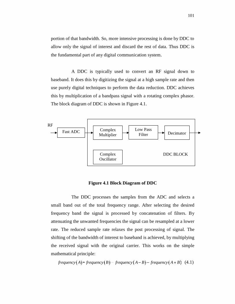
A DDC is typically used to convert an RF signal down to
baseband. It does this by digitizing the signal at a high sample rate and then
use purely digital techniques to perform the data reduction. DDC achieves
this by multiplication of a bandpass signal with a rotating complex phasor.
The block diagram of DDC is shown in Figure 4.1.
Figure 4.1 Block Diagram of DDC
The DDC processes the samples from the ADC and selects a
small band out of the total frequency range. After selecting the desired
frequency band the signal is processed by concatenation of filters. By
attenuating the unwanted frequencies the signal can be resampled at a lower
rate. The reduced sample rate relaxes the post processing of signal. The
shifting of the bandwidth of interest to baseband is achieved, by multiplying
the received signal with the original carrier. This works on the simple
mathematical principle:
frequency A frequency B frequency A B frequency A B (4.1)
RFFast ADC Complex
Multiplier Low Pass
Filter Decimator
ComplexOscillator
DDC BLOCK
102
There are two basic approaches for generating signals directly
from the digital hardware. The first one is commonly referred to as ROM-
LUT approach which is used to generate sinusoidal signal. The sampled
values of sine waveform are stored in ROM and are output periodically
through a DAC to generate the output waveform. If an arbitrary waveform
is to be generated then ROM–LUT is the often used method. CORDIC
provides a convenient approach to compute sinusoidal functionality.
CORDIC algorithms implement transcendental functions without using a
multiplier and by using minimal LUT.
4. 3. 1 ROM-LUT based DDC
By Reed (2002) DDC can conventionally be performed using
ROM-LUT. It is done by multiplying the digitized input signal with
amplitude values of sine and cosine functions stored in a ROM table which
could easily be addressed by the output of an overflowing phase
accumulator.
The ROM-LUT approach uses sampled values of a periodic
function stored in ROM. Every clock cycle, the value of the periodic
function stored in the ROM is output through a DAC to generate the
synthesized signal. The signal obtained at the output of the DAC is then
passed through low pass filters and amplifier to obtain the final output
analog waveform. ROM-LUT employs function generators based on a
single crystal oscillator to generate a reference clock frequency. The
structure of ROM-LUT based DDC system shown in Figure 4.2.

103
Figure 4.2 Block Diagram of ROM - LUT DDC
The adder and address register functions as an accumulator and
increments the output phase value by at each clock cycle. is defined
as free setting word. The output of the accumulator takes the form of an
adder used by a ROM-LUT that contains the waveform samples. The
number of clock cycles needed to step through the entire ROM-LUT
defines the period of the waveform. Hence the waveform period is
determined by . The LUT holds the digital representation of the desired
waveform which is made of digital words that define the amplitude of the
waveform as a function of phase. The address generated by the adder
represents the phase value of the waveform.
The address generator sequentially reads the table of digital
values from the memory and passes them to the DAC to generate the output
waveform. The DAC changes each of these digital words into an analog
voltage, fed through filters to reduce the distortion and amplifiers to
produce an analog signal. The period of the output waveform is based on
the phase increment value and the frequency of the clock signal clkF . As
the size of the ROM needed is the major design issue it is necessary to limit
the address size. To output a particular frequency, the proper phase
104
increment value must be loaded into the accumulator. The original address
is increased by the phase increment and is used to index the ROM- LUT.
According to nyquist sampling criteria, the maximum value of lowpass
output frequency can be given by
2out clkF F (4.2)
The desired resolutions of this frequency output from the ROM-
LUT affects the size of the accumulator and hence the size of LUT. For a
smallest change of =1, the frequency resolution is given by
clkF F ACM (4.3)
where clkF --- system clock
The size of accumulator ACM is given by
NACM (4.4)
where N --- number of bits in accumulator.
Since the transformation in the LUT is non linear, the output frequency, out clkF F ACM (4.5)
The size of phase increment can be calculated using
out clkF F ACM (4.6)
where outF --- desired output frequency in the ROM-LUT.
Lack of spectral purity and sideband noise are the major defect
of this system. Amplitude truncation, phase truncation and DAC non-
linearity are the sources of spurious signals. For a high resolution of n bits it
requires a LUT of 2n n bits resulting in high power consumption, low
speed and increased cost.
105
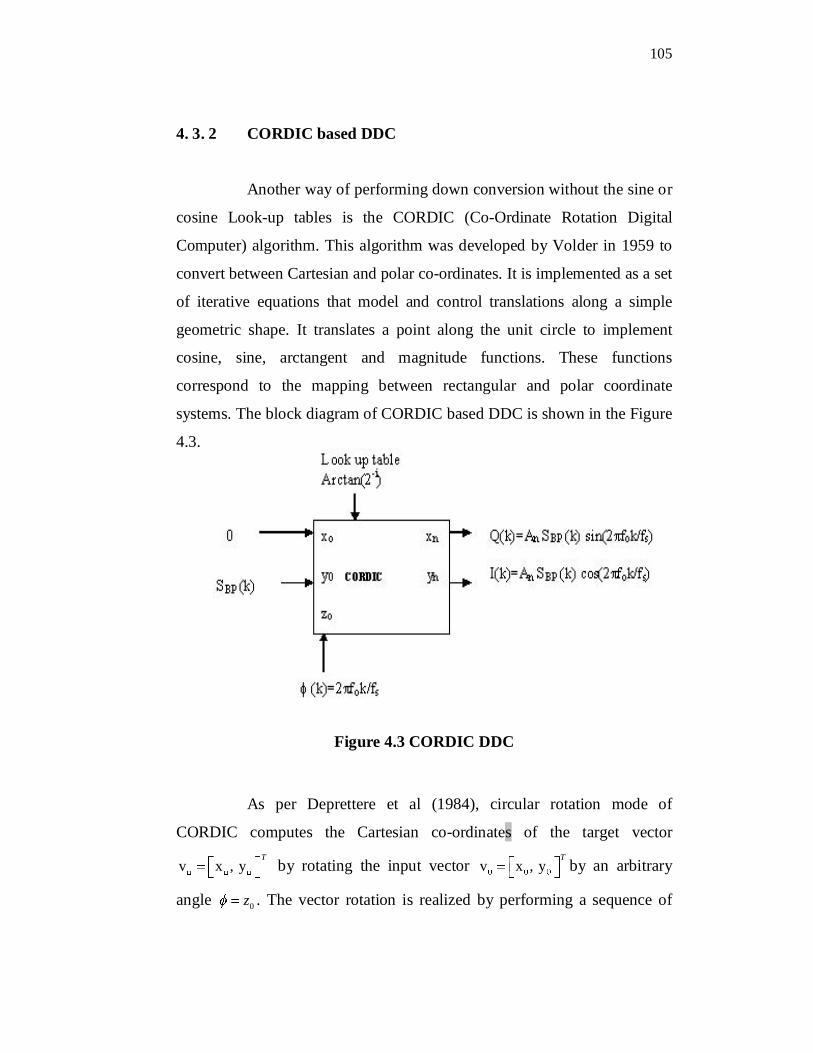
4. 3. 2 CORDIC based DDC
Another way of performing down conversion without the sine or
cosine Look-up tables is the CORDIC (Co-Ordinate Rotation Digital
Computer) algorithm. This algorithm was developed by Volder in 1959 to
convert between Cartesian and polar co-ordinates. It is implemented as a set
of iterative equations that model and control translations along a simple
geometric shape. It translates a point along the unit circle to implement
cosine, sine, arctangent and magnitude functions. These functions
correspond to the mapping between rectangular and polar coordinate
systems. The block diagram of CORDIC based DDC is shown in the Figure
4.3.
Figure 4.3 CORDIC DDC
As per Deprettere et al (1984), circular rotation mode of
CORDIC computes the Cartesian co-ordinates of the target vector
v x , yT
by rotating the input vector v x , yT
by an arbitrary
angle 0z . The vector rotation is realized by performing a sequence of
106
successively decreasing elementary rotation angles arctan 2 ii for
i=0,1,… n-1.
According to Reed (2002) after n iterations the results of
CORDIC algorithm takes the following form
n 0 0 0 0x x cos y cos nA z z (4.7a)
n 0 0 0 0y y cos x cosnA z z (4.7b)
n 0z (4.7c)
An is CORDIC scaling factor that depends on the total number of
iterations n and can be calculated by
2
01 2
ni
ni
A (4.7d)
The accuracy is determined by a number of iterations and the
word length of the CORDIC processor. At each clock interval, yo is loaded
with the current sample SBP (k) of an IF input signal, z0 with the current
sample (k) and xo is set to zero. After n+1 iterations the CORDIC provides
the sample values of the down converted I(k) and Q(k) signal with a
resolution of approximately n bits. In order to achieve this, only a very
small look up table is needed. It contains the (n+2) basic rotation angles.
As mentioned by Andarka (1998) and Wang et al (1996)
CORDIC can be implemented using pipelined architecture. Thus, it is
suitable for high speed applications. An additional advantage of such
implementation is that there is no need for a LUT anymore, since the
invariant elementary rotation angles can be hard-wired in each stage. The
hardware required for a word length the CORDIC is approximately three
multipliers. This means that CORDIC DDC has only one and a half of the
107
hardware complexity of the common DDC while saving a large amount of
chip area because no ROM table is needed.
4. 4 SAMPLE RATE CONVERSION
Since different communication standards are based on different
master clock rates, it is necessary to provide these clock rates separately.
Due to the strong requirement of clock quality, it is reasonable to assume
that only one fixed master clock will be provided in practical SDR
applications. Thus the solution is to provide different clock rates virtually
by means of digital sample rate conversion (SRC). Hence, with the advent
of SDR, a new functionality has to be introduced to the signal processing of
digital communications transceivers. SRC does the task of converting the
sample rate of a digital signal to another sample rate while preserving a
certain amount of information usually in a limited frequency band.
In multi-standard applications SRC helps to efficiently convert
signals received from the antenna to be digitized at ADC sampling
frequency at a data rate that can be conveniently processed by the existing
DSP processors. There are two classes of sample rate converters. The first
class is synchronous and the second one is asynchronous. In synchronous
sample rate converters the sample rate of incoming signal is converted to a
new sample rate by an integer factor. It produces the output samples at a
fixed rate with respect to the input samples. It is not suitable for many
applications as problem appears if irrational conversion factors are needed.
On the other hand, output sample rate of asynchronous sample rate
converters are independent of the input sample rate as dealt in Wang and Li
(2006).

108
There are two methods of sample rate conversion. The first one
uses only analog techniques. Here the idea is to use a DAC in combination
with a brick wall filter. The brick wall filter removes all signal images.
Then the ADC converts signal back to a digital format. The ADC runs at
the output sampling rate. Figure 4.4 shows the block diagram of analog
DDC design. But the main problem of this method is that analog functions
are more difficult to implement. So it is not used practically. Hence an all-
digital solution is more preferred. The general principle of all-digital sample
rate converter is almost analogous to the analog technique except that the
Brick Wall filter is replaced by a digital interpolation filter. The block
diagram of all-digital sample rate converter is shown in Figure 4.5.
Figure 4.4 Analog Method of Sample Rate Conversion
Figure 4.5 All- Digital Method of Sample Rate Conversion
Interpolator
Digital Filtery(m)
x(n)
109
4. 4. 1 Methods of realization of SRC in SDR terminals
An approach is to oversample and band-limit the signal which
eventually enables the application of the interpolation. The
disadvantage of this approach is that it requires high sample rates and
anti-imaging filters for attenuating the images caused by
oversampling. The digital filter for interpolation is being implemented
in the time-continuous envelope of the impulse response and not on
the samples of the already stored fixed impulse response. Therefore
the required coefficients are determined at the run time. The
conventional interpolation is not well suited for realizing SRC in
mobile communication terminals due to their lack of aliasing –
component attention. Therefore, the structures have to perform anti-
aliasing while keeping the efforts sufficiently low.
The second approach is the approximation of arbitrary impulse
responses done by piecewise polynomials. Such impulse responses can
be implemented on the Farrow structure, but it requires sophisticated
controlling.
Finally, comb filters for attenuating potential aliasing components can
be implemented as cascaded integrator comb (CIC) filters. These are
highly efficient multiplier-less filters either to increase or decrease
sample rate by integer factors. Combining both filters for up and
downsampling yields a system performing rational factor SRC.

110
4. 4. 2 Cascaded Integrate Comb Filter
As data converters become faster and faster the extraction and
construction of narrowband signal from wideband sources are becoming
more important. These functions require two basic signal processing
procedures: decimation and interpolation. A typical interpolator consists of
an interpolation filter which is purely an anti-imaging filter and an
upsampler. Correspondingly, a standard decimator has an anti-aliasing filter
and downsampler.
While digital hardware is becoming faster there is still the need
for efficient solutions. Performing interpolation and decimation devised a
flexible, multiplier-free filter suitable for hardware implementation that can
handle arbitrary and large rate changes.
The disadvantage of a cascade of interpolator and decimator is
generally the high intermediate sample rate at which the filters have to
operate. However, by exploiting the fact that the input given to the filters is
zero-padded by the upsampling process the implementation of CIC filters is
possible. These filters run at the input sample rate rather than the
intermediate rate. The resulting CIC filters are a very efficient means of
executing SRC. While the first two suggestions can principally perform
SRC by real factors, leady to a non-periodical time-varying filter (in case of
irrational factors), the latter can execute only rational factor SRC, leading to
a periodically time- varying filter. Still the restriction on rational factors
does not really limit the applicability as it approximates any real factor.
Moreover, as the symbol or chip rate of the different standards can be
represented by integer numbers, there is always a rational factor conversion
between these rates.
111
There are two basic types of Sample rate converters: Fractional-
factor SRC and Integer factor SRC. In the front-end of SDR receiver,
decimator is of most interest, since the over sample ratio (OSR) is relatively
high. If integer factor decimator is implemented in the front stage, time-
varying CIC filter is an ideal choice. It requires small chip area and is
suitable for implementation in ASIC or FPGA. CIC filter is a multiplier-less
lowpass filter. This feature enables CIC filter to handle the high data rate at
the front-end. CIC filter performs SRC efficiently by using additions/
subtractions in the receiver with the highest sample rates as quoted by
Hogenauer (1981) and Wasserman and Willson Jr. (1999). Another reason
restricts CIC filter be implemented only in the front stage is that CIC filter
has a small stop-band and a relatively wide transition-band. This makes
CIC filter should work in a high OSR environment.
In applications where power consumption is an issue, low
complexity solutions are sought for. Besides offering low complexity they
realization of filters is independent of rate-change factor.
Mayer-Baese (2004) has shown that CIC filter has three basic blocks such
as integrators, combs and a downsampling/ upsampling stages.
The integrator is simply a single – pole IIR filter with unity
feedback coefficient. It can also be called as accumulator. The integrator
operating at high sampling rate Fs is realized by the transfer function,
11 1F z z (4.8)
Comb filter does the delay and subtract on the current sample.
The comb block can be treated as a discrete time differentiator. It is
implemented as a digital programmable delay chain followed by a
112
subtractor. The comb blocks operating at low sampling rate (Fs /R) can be
represented as,
1 RDF z z (4.9)
where D---number of delays in the C section usually called as
differential delay
R--- down sampling factor or integer rate change factor
A typical CIC filter consisting of a recursive integrator (I
section), a decimator and a differentiator (C section). To build a CIC filter,
output is cascaded to input with S integrator sections and S comb sections
chained together. It has following transfer function
11 1 sRDF z z z (4.10)
where S --- number of the stages of filter
More compactly the equation (4.10) of CIC filter can be
represented as
1
0
sRDk
k
F z z (4.11)
Since all the coefficients of the IIR filters are unity and
symmetric, CIC filter has a linear phase response and constant group delay.
The passband attenuation is a function of the number of stages (S). Increase
in the number of stages improves the imaging or alias rejection and hence
increase the passband droop. CIC filters are useful for systems requiring a
large rate change factor. The simplicity of the filter structure significantly
reduces the complexity of the design, without any multiplier resources,
making it more resource efficient.
113
4. 5 RESULTS AND DISCUSSION
In this thesis two methods the CORDIC, ROM-LUT based
Digital down conversions are proposed. The simulation results are
presented in this section compare the performance of the above said
algorithms in the design of DDC. The scheme of design is simulated using
MATLAB. /4 DQPSK Modulation signal is being transmitted over the
AWGN channel. The assumption is made that the channel acts as an ideal
channel with the gain equal to one. At different SNR values Bit Error Rate
(BER) and Average Bit Error Rate (AvBER) are calculated using both the
methods. Figure 4.6 shows the plot of BER versus number of iterations of
CORDIC method. The plot shows that BER of CORDIC method remains a
constant value for more than 11 iterations hence the optimum number of
iterations to be executed is 12. Hence increasing the number of iterations
does not have any effect in the performance improvement of CORDIC
DDC.
Figure 4.7 shows the BER of ROM-LUT method is constantly
increasing value for upto 15 iterations. Therefore more number of iterations
is required. While analyzing the Figure 4.8 and 4.9 it is found that for
CORDIC average BER is a decreasing quantity where as it is more for
ROM-LUT. So the conclusion can be made that CORDIC has better
performance over ROM-LUT.
The result shows that CORDIC based method overcomes the
limitations of ROM-LUT of requiring a very large ROM table to achieve
high resolution. Hence CORDIC method helps to save chip area, power
consumption and cost. Since CORDIC can be easily implemented using
pipelined architecture, it is suitable for high-speed wireless application.

114
CIC is most suited for SDR implementation since:
No multipliers are required
No storage is required for filter coefficient
Structure of CIC filter is regular and it has two simple blocks
Very little complicated control is needed
Figure 4.6 BER vs. number of iterations for CORDIC DDC
Figure 4.7 BER vs. number of iteration for ROM -LUT DDC
00.10.20.30.40.5
12 13 14 15 16n iteration
00.05 0.1
0.15 0.2
0.25 0.3
12 13 14 15 16 17
n iteration
115
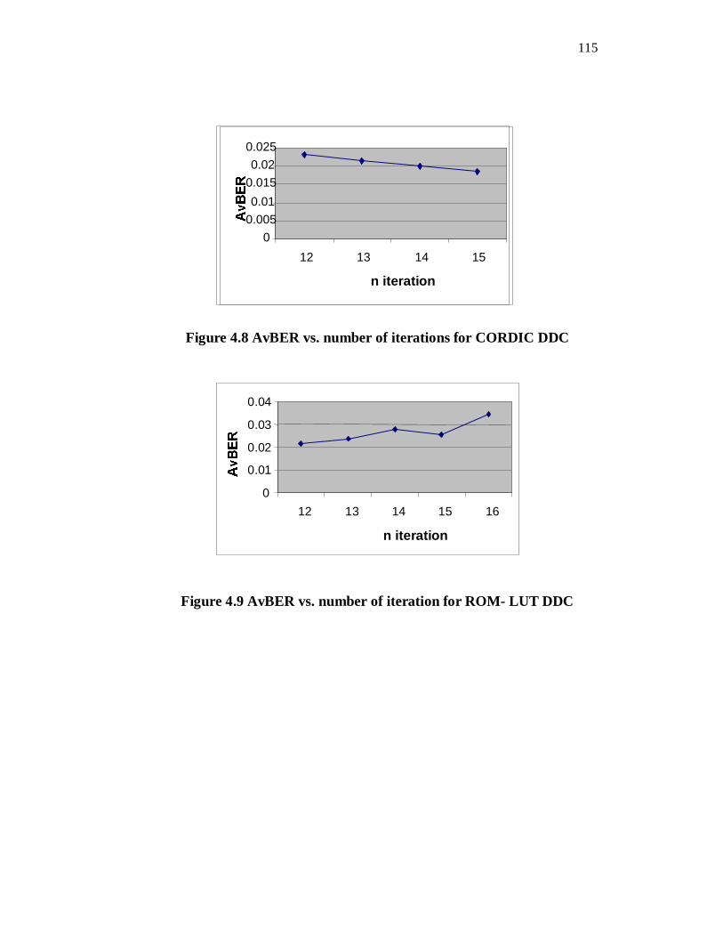
Figure 4.8 AvBER vs. number of iterations for CORDIC DDC
Figure 4.9 AvBER vs. number of iteration for ROM- LUT DDC
0
0.01
0.02
0.03
0.04
12 13 14 15 16
n iteration
0 0.0050.01
0.0150.02
0.025
12 13 14 15
n iteration

116
Figure 4.10 PSD of IF waveform
Figure 4.11 PSD of output waveform from the transmitter for the
input 1 0 1 0 1 1 0 0 1 1
117
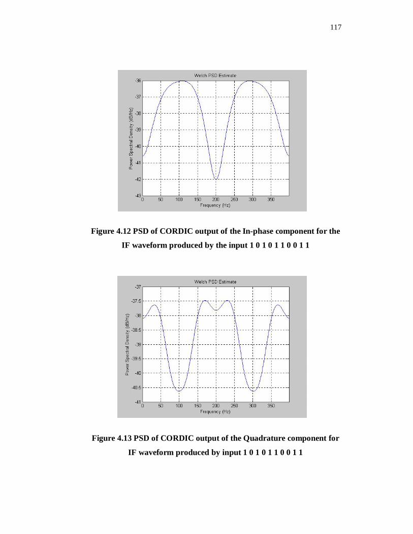
Figure 4.12 PSD of CORDIC output of the In-phase component for the
IF waveform produced by the input 1 0 1 0 1 1 0 0 1 1
Figure 4.13 PSD of CORDIC output of the Quadrature component for
IF waveform produced by input 1 0 1 0 1 1 0 0 1 1