Embed Size (px)
Citation preview
CHAPTER 36 OPTICAL PROPERTIES OF SEMICONDUCTORS
Paul M . Amirtharaj and David G . Seiler Materials Technology Group Semiconductor Electronics Di y ision National Institute of Standards and Technology Gaithersburg , Maryland
3 6 . 1 GLOSSARY
A power absorption
B magnetic field
c velocity of light
D displacement field
d film thickness
E applied electric field
E c energy , conduction band
E e x exciton binding energy
E g energy band gap
E H hydrogen atom ionization energy 5 13 . 6 eV
E electric field
E Ú
n Landau level energy
E y energy , valence band
e I ionic charge
g * ef fective g-factor
K phonon wave vector
k extinction coef ficient
k B Boltzmann’s constant
k electron / hole wave vector
L Ú coupled LO phonon – plasmon frequency
m * e electron ef fective mass
m * h hole ef fective mass
36 .1

36 .2 OPTICAL AND PHYSICAL PROPERTIES OF MATERIALS
m i ionic mass
m 9 i reduced ionic mass
m i m p impurity ion mass
m * l longitudinal ef fective mass
m o electron rest mass
m r electron-hole reduced mass
m * t transverse ef fective mass
N volume density
n refractive index (real part)
n 5 ( n 1 ik ) complex index of refraction
P polarization field
q photon wave vector
R power reflection
R y ef fective Rydberg
S oscillator strength
T power transmission
T temperature
V Verdet coef ficient
a absorption coef ficient
a A D absorption coef ficient , allowed-direct transitions
a A I absorption coef ficient , allowed-indirect transitions
a F D absorption coef ficient , forbidden-direct transitions
a F I absorption coef ficient , forbidden-indirect transitions
d skin depth or penetration depth
g phenomenological damping parameter
D spin-orbit splitting energy
G Brillouin zone center
e dielectric function
e f c ( v ) free-carrier dielectric function
e i m p ( v ) impurity dielectric function
e i n t ( v ) intrinsic dielectric function
e l a t ( v ) lattice dielectric function
e (0) static dielectric constant
e 0 free-space permittivity
e 1 Real ( e )
OPTICAL PROPERTIES OF SEMICONDUCTORS 36 .3
e 2 Im ( e )
e high-frequency limit of dielectric function
h impurity ion charge
l wavelength
l c cut-of f wavelength
m mobility
m B Bohr magneton
… frequency
s conductivity
τ scattering time
f work function
χ susceptibility
χ ( n ) induced nonlinear susceptibility
Ω phonon frequency
v angular frequency
v c cyclotron resonance frequency
v L O longitudinal optical phonon frequency
v p free-carrier plasma frequency
v p v valence band plasma frequency
v T O transverse optical phonon frequency
3 6 . 2 INTRODUCTION
Rapid advances in semiconductor manufacturing and associated technologies have increased the need for optical characterization techniques for materials analysis and in-situ monitoring / control applications . Optical measurements have many unique and attractive features for studying and characterizing semiconductor properties : (1) They are contact- less , nondestructive , and compatible with any transparent ambient including high-vacuum environments ; (2) they are capable of remote sensing , and hence are useful for in-situ analysis on growth and processing systems ; (3) the high lateral resolution inherent in optical systems may be harnessed to obtain spatial maps of important properties of the semiconductor wafers or devices ; (4) combined with the submonolayer sensitivity of a technique such as ellipsometry , optical measurements lead to unsurpassed analytical details ; (5) the resolution in time obtainable using short laser pulses allows ultrafast phenomena to be investigated ; (6) the use of multichannel detection and high-speed computers can be harnessed for extremely rapid data acquisition and reduction which is crucial for real-time monitoring applications such as in in-situ sensing ; (7) they provide information that complements transport analyses of impurity or defect and electrical behavior ; (8) they possess the ability to provide long-range , crystal-like properties and

36 .4 OPTICAL AND PHYSICAL PROPERTIES OF MATERIALS
hence support and complement chemical and elemental analyses ; and (9) finally , most optical techniques are ‘‘table-top’’ procedures that can be implemented by semiconductor device manufacturers at a reasonable cost . All optical measurements of semiconductors rely on a fundamental understanding of their optical properties . In this chapter , a broad overview of the optical properties of semiconductors is given , along with numerous specific examples .
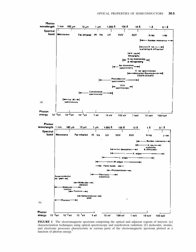
The optical properties of a semiconductor can be defined as any property that involves the interaction between electromagnetic radiation or light and the semiconductor , including absorption , dif fraction , polarization , reflection , refraction , and scattering ef fects . The electromagnetic spectrum is an important vehicle for giving an overview of the types of measurements and physical processes characteristic of various regions of interest involving the optical properties of semiconductors . The electromagnetic spectrum acces- sible for studies by optical radiation is depicted in Fig . 1 a and b where both the photon wavelengths and photon energies , as well as the common designations for the spectral bands , are given . 1 Figure 1 a shows the various techniques and spectroscopies and their spectral regions of applicability . Molecular , atomic , and electronic processes characteristic of various parts of the spectrum are shown in Fig . 1 b . The high-energy x-ray , photoelectron , and ion desorption processes are important to show because they overlap the region of vacuum ultraviolet (VUV) spectroscopy . The ultraviolet (UV) region of the spectrum has often been divided into three rough regions : (1) the near-UV , between 2000 and 4500 Å ; (2) the VUV , 2000 Å down to about 400 Å ; and (3) the region below 400 Å covering the range of soft x-rays , 10 to 400 Å . 2 The spectrum thus covers a broad frequency range which is limited at the high-frequency end by the condition that l a , where l is the wavelength of the light wave in the material and a is the interatomic distance . This limits the optical range to somewhere in the soft x-ray region . Technical dif ficulties become severe in the ultraviolet region (less the 100-nm wavelength , or greater than 12 . 3-eV photon energies) , and synchrotron radiation produced by accelerators can be utilized ef fectively for ultraviolet and x-ray spectroscopy without the limitations of conventional laboratory sources . A lower limit of the optical frequency range might correspond to wavelengths of about 1 mm (photon energy of 1 . 23 3 10 2 3 eV) . This ef fectively excludes the microwave and radio-frequency ranges from being discussed in a chapter on the optical properties of semiconductors .
From the macroscopic viewpoint , the interaction of matter with electromagnetic radiation is described by Maxwell’s equations . The optical properties of matter are introduced into these equations as the constants characterizing the medium such as the dielectric constant , magnetic permeability , and electrical conductivity . (They are not real ‘‘constants’’ since they vary with frequency . ) From our optical viewpoint , we choose to describe the solid by the dielectric constant or dielectric function e ( v ) . This dielectric constant is a function of the space and time variables and should be considered as a response function or linear integral operator . It can be related in a fundamental way to the crystal’s refractive index n and extinction coef ficient k by means of the Kramers-Kro nig dispersion relations as discussed later . It is the values of the optical constants n and k that are usually directly measured in most optical experiments ; they are real and positive numbers .
There are a number of methods for determining the optical constants n and k of a semiconductor as a function of wavelength . Five of the most common techniques are as follows .
1 . Measure the reflectivity at normal incidence over a wide wavelength and use a Kramers-Kro nig dispersion relation .
2 . Measure the transmission of a thin slab of known thickness together with the absolute reflectivity at normal incidence or alternately observe the transmission over a wide spectral range and obtain n by a Kramers-Kro nig analysis .
OPTICAL PROPERTIES OF SEMICONDUCTORS 36 .5
FIGURE 1 The electromagnetic spectrum comprising the optical and adjacent regions of interest : ( a ) characterization techniques using optical spectroscopy and synchrotron radiation ; ( b ) molecular , atomic , and electronic processes characteristic in various parts of the electromagnetic spectrum plotted as a function of photon energy . 1

36 .6 OPTICAL AND PHYSICAL PROPERTIES OF MATERIALS
3 . Measure the reflection of unpolarized light at two or more angles of incidence . 4 . Use a polarimetric method like ellipsometry which involves finding the ratio of
reflectivities perpendicular and parallel to the plane of incidence at a nonnormal incidence together with the dif ference of phase shifts upon reflection .
5 . Use detailed computer modeling and fitting of either reflection , transmission , or ellipsometric measurements over a large enough energy range .
These optical constants describe an electromagnetic wave in the medium of propagation ; the refractive index n gives the phase shift of the wave , and the extinction coef ficient or attenuation index k gives the attenuation of the wave . In practice , one often uses the absorption coef ficient a instead of k because of the Beer’s low formalism describing the absorption .
The field of optical spectroscopy is a very important area of science and technology since most of our knowledge about the structure of atoms , molecules , and solids is based upon spectroscopic investigations . For example , studies of the line spectra of atoms in the late 1800s and early 1900s revolutionized our understanding of the atomic structure by elucidating the nature of their electronic energy levels . Similarly for the case of semiconductors , optical spectroscopy has proven essential to acquiring a systematic and fundamental understanding of the nature of semiconductors . Since the early 1950s , detailed knowledge about the various eigenstates present in semiconductors has emerged including energy bands , excitonic levels , impurity and defect levels , densities of states , energy-level widths (lifetimes) , symmetries , and changes in these conditions with tempera- ture , pressure , magnetic field , electric field , etc . One of the purposes of this chapter is to review and summarize the major optical measurement techniques that have been used to investigate the optical properties of semiconductors related to these features . Specific attention is paid to the types of information which can be extracted from such measurements of the optical properties .
Most optical properties of semiconductors are integrally related to the particular nature of their electronic band structures . Their electronic band structures are in turn related to the type of crystallographic structure , the particular atoms , and their bonding . The full symmetry of the space groups is also essential in determining the structure of the energy bands . Group theory makes it possible to classify energy eigenstates , determine essential degeneracies , derive selection rules , and reduce the order of the secular determinants which must be diagonalized in order to compute approximate eigenvalues . Often , experimental measurements must be carried out to provide quantitative numbers for these eigenvalues . A full understanding of the optical properties of semiconductors is thus deeply rooted in the foundations of modern solid-state physics . In writing this chapter , the authors have assumed that the readers are familiar with some aspects of solid-state physics such as can be obtained from an undergraduate course .
Most semiconductors have a diamond , zinc-blende , wurtzite , or rock-salt crystal structure . Elements and binary compounds , which average four valence electrons per atom , preferentially form tetrahedral bonds . A tetrahedral lattice site in a compound AB is one in which each atom A is surrounded symmetrically by four nearest neighboring B atoms . The most important lattices with a tetrahedral arrangement are the diamond , zinc-blende , and wurtzite lattices . In the diamond structure , all atoms are identical , whereas the zinc-blende structure contains two dif ferent atoms . The wurtzite structure is in the hexagonal crystal class , whereas the diamond and zinc-blende structures are cubic . Other lattices exist which are distorted forms of these and others which have no relation to the tetrahedral structures .
Band structure calculations show that only the valence band states are important for predicting the following crystal ground-state properties : charge density , Compton profile , compressibility , cohesive energy , lattice parameters , x-ray emission spectra , and hole

OPTICAL PROPERTIES OF SEMICONDUCTORS 36 .7
ef fective mass . In contrast , both the valence-band and conduction-band states are important for predicting the following properties : optical dielectric constant or refractive index , optical absorption spectrum , and electron ef fective mass . Further complexities arise because of the many-body nature of the particle interactions which necessitates under- standing excitons , electron-hole droplets , polarons , polaritons , etc .
The optical properties of semiconductors cover a wide range of phenomena which are impossible to do justice to in just one short chapter in this Handbook . We have thus chosen to present an extensive , systematic overview of the field , with as many details given as possible . The definitions of the various optical properties , the choice of figures used , the tables presented , the references given all help to orient the reader to appreciate various principles and measurements that form the foundations of the optical properties of semiconductors .
The optical properties of semiconductors are often subdivided into those that are electronic and those that are lattice in nature . The electronic properties concern processes involving the electronic states of the semiconductor , while the lattice properties involve vibrations of the lattice (absorption and creation of phonons) . Lattice properties are of considerable interest , but it is the electronic properties which receive the most attention in semiconductors because of the technological importance of their practical applications . Modern-day semiconductor optoelectronic technologies include lasers , light-emitting- diodes , photodetectors , optical amplifiers , modulators , switches , etc ., all of which exploit specific aspects of the electronic optical properties .
Almost all of the transitions that contribute to the optical properties of semiconductors can be described as one-electron transitions . Most of these transitions conserve the crystal momentum and thus measure the vertical energy dif ferences between the conduction and valence bands . In the one-electron approximation , each valence electron is considered as a single particle , moving in a potential which is the sum of the core potentials and a self-consistent Hartree potential of the other valence electrons .
The phenomena usually studied to obtain information on the optical properties of semiconductors are (1) absorption , (2) reflection , (3) photoconductivity , (4) emission , and (5) light scattering . Most of the early information on the optical properties of semiconduc- tors was obtained from measurements of photoconductivity , but these measurements can be complicated by carrier trapping , making interpretation of the results sometimes dif ficult . Thus , most measurements are of the type (1) , (2) , (4) , or (5) . For example , the most direct way of obtaining information about the energy gaps between band extrema and about impurity levels is by measuring the optical absorption over a wide range of wavelengths . Information can also be obtained by (2) and (4) .
The transient nature of the optical properties of semiconductors is important to establish because it gives insight to the various relaxation processes that occur after optical excitation . Because of the basic limitations of semiconductor devices on speed and operational capacity , ultrafast studies have become an extremely important research topic to pursue . The push to extend the technologies in the optoelectronic and telecommunica- tion fields has also led to an explosion in the development and rise of ultrafast laser pulses to probe many of the optical properties of semiconductors : electrons , holes , optical phonons , acoustic phonons , plasmons , magnons , excitions , and the various coupled modes (polaritons , polarons , excitonic molecules , etc . ) . The time scale for many of these excitations is measured in femtoseconds (10 2 1 5 ) or picoseconds (10 2 1 2 ) . Direct time measurements on ultrafast time scales provides basic information on the mechanisms , interactions , and dynamics related to the various optical properties . Some of the processes that have been investigated are the formation time of excitons , the cooling and thermalization rates of hot carriers , the lifetime of phonons , the screening of optical- phonon-carried interactions , the dynamics of ballistic transport , the mechanism of laser annealing , dephasing processes of electrons and excitons , optical Stark ef fect , etc . It is not possible in this short review chapter to cover these ultrafast optical properties of

36 .8 OPTICAL AND PHYSICAL PROPERTIES OF MATERIALS
semiconductors . We refer the reader to the many fine review articles and books devoted to this field . 3 , 4
The advent of the growth of artificially structured materials by methods such as molecular beam epitaxy (MBE) has made possible the development of a new class of materials and heterojunctions with unique electronic and optical properties . Most prominent among these are heterojunction quantum-wells and superlattices . The field of microstructural physics has thus been one of the most active areas of research in the past decade . The novel properties of structures fabricated from ultrathin layers of semiconduc- tors of thicknesses , 100 Å stem from microscopic quantum mechanical ef fects . The simplest case to visualize is that of a particle confined in a box which displays distinct quantum energy states , the equivalent of which are electrons and holes confined to a thin layer of a material such as GaAs sandwiched between two thick layers of AlAs . The new energy states produced by the confinement of the charges in the artificially produced potential well can be manipulated , by tailoring the size and shape of the well , to produce a wide variety of ef fects that are not present in conventional semiconductors . Microstruc- tures formed from alternating thin layers of two semiconductors also lead to novel electronic and optical behavior , most notable of which is large anisotropic properties . The ability to ‘‘engineer’’ the behavior of these microstructures has led to an explosion of research and applications that is too large to be dealt with in this short review . The reader is referred to several review articles on their optical behavior . 5 , 6
3 6 . 3 OPTICAL PROPERTIES
Background
The interaction of the semiconductor with electromagnetic radiation can be described , in the semiclassical regime , using response functions such as e and χ which are defined in the following section . The task of the description is then reduced to that of building a suitable model of χ and e that takes into account the knowledge of the physical characteristics of the semiconductor and the experimentally observed optical behavior . One example of a particularly simple and elegant , yet surprisingly accurate and successful , model of e for most semiconductors is the linear-chain description of lattice vibrations . 7 This model treats the optical phonons , i . e ., the vibrations that have an associated dipole moment , as damped simple harmonic motions . Even though the crystal is made up of , 10 2 3 atoms , such a description with only a few resonant frequencies and phenomenological terms , such as the damping and the ionic charge , accurately accounts for the optical behavior in the far-infrared region . The details of the model are discussed in the following section . Such simple models are very useful and illuminating , but they are applicable only in a limited number of cases , and hence such a description is incomplete .
A complete and accurate description will require a self-consistent quantum mechanical approach that accounts for the microscopic details of the interaction of the incident photon with the specimen and a summation over all possible interactions subject to relevant thermodynamical and statistical mechanical constraints . For example , the absorption of light near the fundamental gap can be described by the process of photon absorption resulting in the excitation of a valence-band electron to the conduction band . In order to obtain the total absorption at a given energy , a summation has to be performed over all the possible states that can participate , such as from multiple valence bands . Thermo- dynamic considerations such as the population of the initial and final states have to be taken into consideration in the calculation as well . Hence , a detailed knowledge of the

OPTICAL PROPERTIES OF SEMICONDUCTORS 36 .9
specimen and the photon-specimen interaction can , in principle , lead to a satisfactory description .
Optical / Dielectric Response
Optical Constants and the Dielectric Function . In the linear regime , the dielectric function e and the susceptibility χ are defined by the following relations 8 :
D 5 e 0 E 1 P (1)
D 5 e 0 (1 1 χ ) E (2)
D 5 e E 5 ( e 1 1 i e 2 ) E (3)
where E , D , and P are the free-space electric field , the displacement field , and the polarization field inside the semiconductor ; e 0 is the permittivity of free space ; and e and χ are dimensionless quantities , each of which can completely describe the optical properties of semiconductors . The refractive index n of the material is related to e as shown below :
n 5 4 e 5 n 1 ik (4)
The real and imaginary parts of the refractive index , n and k , which are also referred to as the optical constants , embody the linear optical property of the material . The presence of k , the imaginary component , denotes absorption of optical energy by the semiconduc- tor . Its relationship to the absorption coef ficient a is discussed in the following section . In the spectral regions where absorptive processes are weak or absent , as in the case of the subband gap range , k is very small , whereas in regions of strong absorption , the magnitude of k is large . The optical constants for a large number of semiconductors may be found in Refs . 9 and 10 . The variation in the real part n is usually much smaller . For example , in GaAs , at room temperature , in the visible and near-visible region extending from 1 . 4 to 6 eV , k varies from , 10 2 3 at 1 . 41 eV which is just below the gap , to a maximum of 4 . 1 at 4 . 94 eV . 1 1 In comparison , n remains nearly constant in the near-gap region extending from 3 . 61 at 1 . 4 eV to 3 . 8 at 1 . 9 eV , with the maximum and minimum values of 1 . 26 at 6 eV and 5 . 1 at 2 . 88 eV , respectively . The real and imaginary components are related by causal relationships that are also discussed in the following sections .
Reflection , Transmission , and Absorption Coef ficients . The reflection and transmission from a surface are given by :
r 5 ( n 2 1) ( n 1 1)
5 u r u ? exp ( i θ ) (5)
R 5 u r 2 u (6)
T 5 (1 2 R ) (7)
where r is the complex reflection coef ficient and R and T are the power reflectance and
36 .10 OPTICAL AND PHYSICAL PROPERTIES OF MATERIALS
transmission . For a thin slab , in free space , with thickness d and refractive index n , the appropriate expressions are 1 2 :
r 5 r 1 1 r 2 ? exp ( i 4 π n d / l ) 1 1 r 1 ? r 2 ? exp ( i 4 π n d / l )
(8)
where r 1 and r 2 are the reflection coef ficients at the first and second interfaces , respectively , and l is the free-space wavelength .
For most cases of optical absorption , the energy absorbed is proportional to the thickness of the specimen . The variation of optical energy inside the absorptive medium is given by the following relationship :
I ( x ) 5 I (0) ? exp ( 2 a ? x ) (9)
and a is related to the optical constants by :
a 5 4 π k / l (10)
Here we note that a (measured in cm 2 1 ) describes the attenuation of the radiation intensity rather than that of the electric field .
In spectral regions of intense absorption , all the energy that enters the medium is absorbed . The only part of the incident energy that remains is that which is reflected at the surface . In such a case , it is useful to define a characteristic ‘‘skin’’ thickness that is subject to an appreciable density of optical energy . A convenient form used widely is simply the inverse of a , i . e ., 1 / a . This skin depth is usually denoted by d :
d 5 1 a
(11)
The skin depths in semiconductors range from . 100 nm near the band gap to , 5 nm at the higher energies of , 6 eV .
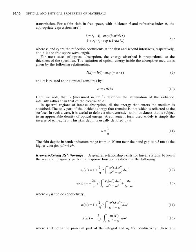
Kramers - Kro nig Relationships . A general relationship exists for linear systems between the real and imaginary parts of a response function as shown in the following :
e 1 ( v ) 5 1 1 2 π
P E
0
v 9 e 2 ( v 9 ) v 9 2 2 v 2 d v 9 (12)
e 2 ( v ) 5 2 2 v
π P E
0
e 1 ( v 9 ) d v 9
v 9 2 2 v 2 1 s 0
e 0 ? v (13)
where s 0 is the dc conductivity .
n ( v ) 5 1 1 2 π
P E
0
v 9 k ( v 9 ) v 9 2 2 v 2 d v 9 (14)
k ( v ) 5 2 2 π
P E
0
n ( v 9 ) v 9 2 2 v 2 d v 9 (15)
where P denotes the principal part of the integral and s 0 the conductivity . These are

OPTICAL PROPERTIES OF SEMICONDUCTORS 36 .11
referred to as the Kramers-Kro nig dispersion relationships . 13 , 14 An expression of practical utility is one in which the experimentally measured power reflection R at normal incidence is explicitly displayed as shown :
θ ( v ) 5 2 v
π P E
0
ln ( R ( v 9 )) d v
v 9 2 2 v 2 (16)
This is useful since it shows that if R is known for all frequencies , θ can be deduced , and hence a complete determination of both n and k can be accomplished . In practice , R can be measured only over a limited energy range , but approximate extrapolations can be made to establish reasonable values of n and k .
The measurement of the reflectivity over a large energy range spanning the infrared to the vacuum ultraviolet , 0 . 5- to 12-eV range , followed by a Kramers-Kro nig analysis , used to be the main method of establishing n and k . 1 5 However , the advances in spectroscopic ellipsometry in the past 20 years have made this obsolete in all but the highest energy region . A discussion of the past methods follows for completeness .
The measured reflectivity range , in general , is not large enough to obtain accurate values of n and k . Hence , extrapolation procedures were used to guess the value of R beyond , 12 eV . 1 5 The most justifiable procedure , from a physical standpoint , assumed that the higher energy reflectivity was dominated by the valence-band plasma edge v P V and , hence , assumed the following forms for e ( v ) , n ( v ) , and R ( v ) :
n 5 4 e ( v ) < 2 1 2
? S v 2 PV
v 2 D (17)
R ( v ) 5 ( n ( v ) 2 1) ( n ( v ) 1 1)
5 1
16 ? S v 4
PV
v 4 D (18)
Other less intuitive forms of extrapolations have also been used with an exponential fallof f or a v 2 p fall where p is computer fit to get the most consistent results .
Sum Rules . Having realized the interrelationships between the real and imaginary parts of the response functions , one may extend them further using a knowledge of the physical properties of the semiconductor to arrive at specific equations , commonly referred to as sum rules . 13 , 14 These equations are useful in cross-checking calculations for internal consistency or reducing the computational ef fort . Some of the often-used relations are shown below :
E
0 v e 2 ( v ) d v 5
π 2
v 2 PV (19)
E
0 v Im F 2 1
e ( v ) G d v 5
π 2
v 2 PV
(20)
E
0 v k ( v ) ? d v 5
π 4
v 2 PV
(21)
E
0 [ n ( v ) 2 1] d v 5 0 (22)
where v P V is the valence-band plasma frequency .
36 .12 OPTICAL AND PHYSICAL PROPERTIES OF MATERIALS
The dc static dielectric constant , e (0) may be expressed as :
e (0) 5 1 1 2 π E
0
e 2 ( v ) v
? d v (23)
The reader is referred to Refs . 13 and 14 for more details .
Linear Optical Properties
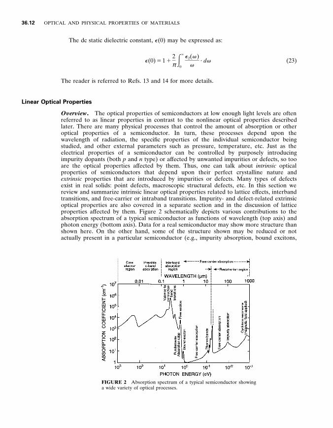
O y er y iew . The optical properties of semiconductors at low enough light levels are often referred to as linear properties in contrast to the nonlinear optical properties described later . There are many physical processes that control the amount of absorption or other optical properties of a semiconductor . In turn , these processes depend upon the wavelength of radiation , the specific properties of the individual semiconductor being studied , and other external parameters such as pressure , temperature , etc . Just as the electrical properties of a semiconductor can be controlled by purposely introducing impurity dopants (both p and n type) or af fected by unwanted impurities or defects , so too are the optical properties af fected by them . Thus , one can talk about intrinsic optical properties of semiconductors that depend upon their perfect crystalline nature and extrinsic properties that are introduced by impurities or defects . Many types of defects exist in real solids : point defects , macroscopic structural defects , etc . In this section we review and summarize intrinsic linear optical properties related to lattice ef fects , interband transitions , and free-carrier or intraband transitions . Impurity- and defect-related extrinsic optical properties are also covered in a separate section and in the discussion of lattice properties af fected by them . Figure 2 schematically depicts various contributions to the absorption spectrum of a typical semiconductor as functions of wavelength (top axis) and photon energy (bottom axis) . Data for a real semiconductor may show more structure than shown here . On the other hand , some of the structure shown may be reduced or not actually present in a particular semiconductor (e . g ., impurity absorption , bound excitons ,
FIGURE 2 Absorption spectrum of a typical semiconductor showing a wide variety of optical processes .

OPTICAL PROPERTIES OF SEMICONDUCTORS 36 .13
TABLE 1 Classification by Wavelength of the Optical Responses for Common Semiconductors
Wavelength (nm) Responses Physical origin Application Measurement
tech .
l . l T O Microwave R and T Free-carrier plasma Detectors R , T , and A * Far-IR and micro-
wave region Plasma R and T Switches Microwave techniques
Fourier Transform Spectrometry (FTS)
l L O , l , l T O Reststrahlen region
Reststrahlen R Optical phonons in ionic crystals
Absorbers R , T , and A Filters FTS & Dispersion
spectrometry (DS)
l , l L O , l T O , l P Far-IR region
Far-IR A Optical phonons , impurities (vibration and electronic) , free carriers , intervalence transitions
Absorbers Filters
R , T , and A FTS and DS
l L O . l . l G Mid-IR region
Mid-IR T and A Multiphonon , multiphoton transitions , impurities (vibrational and electronic) , intervalence transitions excitons , Urbach tail
Detectors Switches Absorbers Filters
R , T , and A Ellipsometry FTS and DS
l , l G IR , visible , and UV
R , T , and A Electronic interband transitions
Reflectors Detectors
Reflection Ellipsometry
l , l W UV , far-UV
Photoemission Fermi energy to vacuum-level electronic transitions
Photocathodes Detectors
High-vacuum , spectroscopy tech .
l W . l . * a R , T , and A Ionic-core transitions Detectors Soft x-ray and synchrotron-based analyses
Dif fraction Photo—ionic-core interactions
X-ray optics and mono- chromators
X-ray techniques
* R , T , and A —Reflection , transmission , and absorption . Note : P—Plasma ; G—Energy gap ; W—Work functions ; (a lattice constant) . TO , LO : Transverse and longitudinal optical phonons .
d-band absorption) . Table 1 shows the classification of the optical responses of the semiconductor to light in various wavelength regions showing the typical origin of the response and how the measurements are usually carried out . At the longest wavelengths shown in Fig . 2 , cyclotron resonance may occur for a semiconductor in a magnetic field , giving rise to an absorption peak corresponding to a transition of a few meV energy between Landau levels . Shallow impurities may give rise to additional absorption at low temperatures and here a 10-meV ionization energy has been assumed . If the temperature was high enough so that k B T was greater than the ionization energy , the absorption peak would be washed out . At wavelengths between 20 to 50 m m , a new set of absorption peaks arises due to the vibrational modes of the lattice . In ionic crystals , the absorption coef ficient in the reststrahlen region may reach 10 5 cm 2 1 , whereas in homopolar semicon-
36 .14 OPTICAL AND PHYSICAL PROPERTIES OF MATERIALS
ductors like Si and Ge , only multiphonon features with lower absorption coef ficients are present (around 5 to 50 cm 2 1 ) .
Models of the Dielectric Function . The interaction of light with semiconductors can be completely described by the dielectric function , e ( v ) . The dielectric function e ( v ) may be divided into independent parts to describe various physical mechanisms so long as the processes do not interact strongly with each other ; this is an approximation , referred to as the adiabatic approximation which simplifies the task at hand considerably . 1 6 The major players that determine the optical behavior of an intrinsic semiconductor are the lattice , particularly in a nonelemental semiconductor ; the free carriers , i . e ., mobile electrons and holes ; and the interband transitions between the energy states available to the electrons . These three mechanisms account for the intrinsic linear properties that lead to a dielectric function as shown :
e int ( v ) 5 e lat ( v ) 1 e f c ( v ) 1 e inter ( v ) (24)
The addition of impurities and dopants that are critical to controlling the electronic properties leads to an additional contribution , and the total dielectric response may then be described as shown :
e ( v ) 5 e int ( v ) 1 e imp ( v ) (25)
Lattice Phonons . The dc static response of a semiconductor lattice devoid of free charges to
an external electromagnetic field may be described by the single real quantity e (0) . As the frequency of the electromagnetic radiation increases and approaches the characteristic vibrational frequencies associated with the lattice , strong interactions can occur and modify the dielectric function substantially . The main mechanism of the interaction is the coupling between the electromagnetic field with the oscillating dipoles associated with vibrations of an ionic lattice . 7 The interactions may be described , quite successfully , by treating the solid to be a collection of damped harmonic oscillators with a characteristic vibrational frequency v T O and damping constant g . The resultant dielectric function may be written in the widely used CGS units as :
e lat ( v ) 5 e ( ) 1 S v 2
TO
( v 2 TO 2 v 2 2 i v g )
(26)
where S is called the oscillator strength and may be related to the phenomenological ionic charge e i , reduced mass m 9 i , and volume density N , through the equation
S v 2 TO 5
4 π Ne 2 1
m 9 i (27)
In the high frequency limit of e ( v ) , for v v T O ,
e ( v ) 5 e (28)
The relationship may be easily extended to accommodate more than one characteristic vibrational frequency by the following relationship :
e lat ( v ) 5 e 1 O j
S j ( v j TO ) 2
[( v j TO ) 2 2 v 2 2 i v g j ]
(29)
OPTICAL PROPERTIES OF SEMICONDUCTORS 36 .15
It is worth noting some important physical implications and interrelations of the various parameters in Eq . (26) .
For a lattice with no damping , it is obvious that e ( v ) displays a pole at v T O and a zero at a well-defined frequency , usually referred to by v L O . A simple but elegant and useful relationship exists between these parameters as shown by
e (0) e
5 S v L O
v T O D 2
(30)
which is known as the Lydenne-Sachs-Tellers relationship . 1 7
The physical significance of v T O and v L O is that these are the transverse and longitudinal optical phonon frequencies with zero wave vector , K , supported by the crystal lattice . The optical vibrations are similar to standing waves on a string . The wave pattern , combined with the ionic charge distribution , leads to oscillating dipoles that can interact with the incident radiation and , hence , the name optical phonons . e ( v ) is negative for v T O $ v $ v L O which implies no light propagation inside the crystal and , hence , total reflection of the incident light . The band of frequencies spanned by v T O and v L O is referred to as the reststrahlen band .
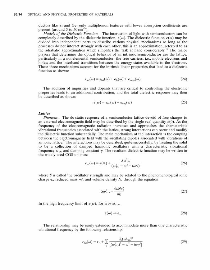
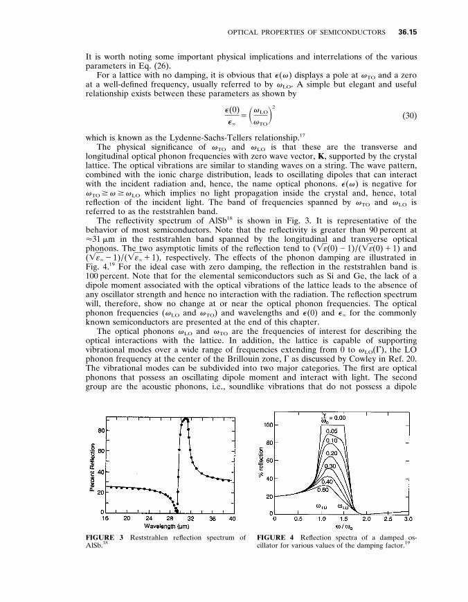
The reflectivity spectrum of AlSb 1 8 is shown in Fig . 3 . It is representative of the behavior of most semiconductors . Note that the reflectivity is greater than 90 percent at < 31 m m in the reststrahlen band spanned by the longitudinal and transverse optical phonons . The two asymptotic limits of the reflection tend to ( 4 » (0) 2 1) / ( 4 » (0) 1 1) and ( 4 » 2 1) / ( 4 » 1 1) , respectively . The ef fects of the phonon damping are illustrated in Fig . 4 . 1 9 For the ideal case with zero damping , the reflection in the reststrahlen band is 100 percent . Note that for the elemental semiconductors such as Si and Ge , the lack of a dipole moment associated with the optical vibrations of the lattice leads to the absence of any oscillator strength and hence no interaction with the radiation . The reflection spectrum will , therefore , show no change at or near the optical phonon frequencies . The optical phonon frequencies ( v L O and v T O ) and wavelengths and e (0) and e for the commonly known semiconductors are presented at the end of this chapter .
The optical phonons v L O and v T O are the frequencies of interest for describing the optical interactions with the lattice . In addition , the lattice is capable of supporting vibrational modes over a wide range of frequencies extending from 0 to v L O ( G ) , the LO phonon frequency at the center of the Brillouin zone , G as discussed by Cowley in Ref . 20 . The vibrational modes can be subdivided into two major categories . The first are optical phonons that possess an oscillating dipole moment and interact with light . The second group are the acoustic phonons , i . e ., soundlike vibrations that do not possess a dipole
FIGURE 3 Reststrahlen reflection spectrum of AlSb . 1 8
FIGURE 4 Reflection spectra of a damped os- cillator for various values of the damping factor . 1 9
36 .16 OPTICAL AND PHYSICAL PROPERTIES OF MATERIALS
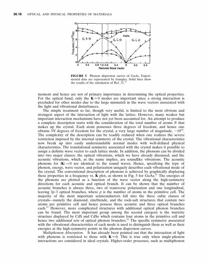
FIGURE 5 Phonon dispersion curves of GaAs . Experi- mental data are represented by triangles . Solid lines show the results of the calculation of Ref . 21 . 2 1
moment and hence are not of primary importance in determining the optical properties . For the optical band , only the K < 0 modes are important since a strong interaction is precluded for other modes due to the large mismatch in the wave vectors associated with the light and vibrational disturbances .
The simple treatment so far , though very useful , is limited to the most obvious and strongest aspect of the interaction of light with the lattice . However , many weaker but important interaction mechanisms have not yet been accounted for . An attempt to produce a complete description starts with the consideration of the total number of atoms N that makes up the crystal . Each atom possesses three degrees of freedom , and hence one obtains 3 N degrees of freedom for the crystal , a very large number of magnitude , , 10 2 4 . The complexity of the description can be readily reduced when one realizes the severe restriction imposed by the internal symmetry of the crystal . The vibrational characteristics now break up into easily understandable normal modes with well-defined physical characteristics . The translational symmetry associated with the crystal makes it possible to assign a definite wave vector to each lattice mode . In addition , the phonons can be divided into two major classes : the optical vibrations , which we have already discussed , and the acoustic vibrations , which , as the name implies , are soundlike vibrations . The acoustic phonons for u K u 5 0 are identical to the sound waves . Hence , specifying the type of phonon , energy , wave vector , and polarization uniquely describes each vibrational mode of the crystal . The conventional description of phonons is achieved by graphically displaying these properties in a frequency vs . K plot , as shown in Fig . 5 for GaAs . 2 1 The energies of the phonons are plotted as a function of the wave vector along the high-symmetry directions for each acoustic and optical branch . It can be shown that the number of acoustic branches is always three , two of transverse polarization and one longitudinal , leaving 3 p -3 optical branches , where p is the number of atoms in the primitive cell . The majority of the most important semiconductors fall into the three cubic classes of crystals—namely the diamond , zincblende , and the rock-salt structures that contain two atoms per primitive cell and hence possess three acoustic and three optical branches each . 2 2 However , more complicated structures with additional optical phonon branches can be found . The most important group among the second category is the wurtzite structure displayed by CdS and CdSe which contains four atoms in the primitive cell and hence two additional sets of optical phonon branches . 2 2 The specific symmetry associated with the vibrational characteristics of each mode is used to distinguish them as well as their energies at the high-symmetry points in the phonon dispersion curves .
Multiphonon Absorption . It has already been pointed out that the interaction of light with phonons is restricted to those with K < 0 . This is true only when single-phonon interactions are considered in ideal crystals . Higher-order processes , such as multiphonon
OPTICAL PROPERTIES OF SEMICONDUCTORS 36 .17
absorption , can activate phonons with K ? 0 . 22 , 23 Symmetry considerations and their implication on the multiphonon absorption are discussed by Birman in Ref . 24 . In multiphonon processes , the total momentum of the interacting phonons will be 0 , but many modes with K ? 0 can participate in the interaction .
The energy and momentum conservation conditions may be expressed as follows :
" v 5 O i
" Ω i (31)
" q 5 O i
" K i < 0 (32)
where " v is the energy of the absorbed photon ; " Ω i is the energy of the phonons ; and " q and " K i are the corresponding momenta . Any number of phonons can participate in the process . However , the strength of interaction between the incident photon and the higher-order processes falls of f rapidly with increasing order , making only the lowest order , i . e ., two- or three-phonon processes noteworthy in most semiconductors . The well-defined range that spans the phonon energies in most semiconductors , extending from 0 to the LO phonon energy at the center of the zone G , restricts the n -phonon process to a maximum energy of n " v L O ( G ) . Among the participating phonons , those with large values of K and those in the vicinity of the critical points are the most important owing to their larger populations . These factors are important in understanding the multiphonon absorption behavior , as we now discuss . 22 , 23
Multiphonon processes may be subdivided into two major categories : (1) sum processes where multiple phonons are created , and (2) dif ference processes in which both phonon creation and annihilation occur with a net absorption in energy . The former process is more probable at higher-incident photon energies and the converse is true for the latter . The reduction of the equilibrium phonon population at low temperatures leads to a lower probability for the dif ference process , and hence it is highly temperature dependent .
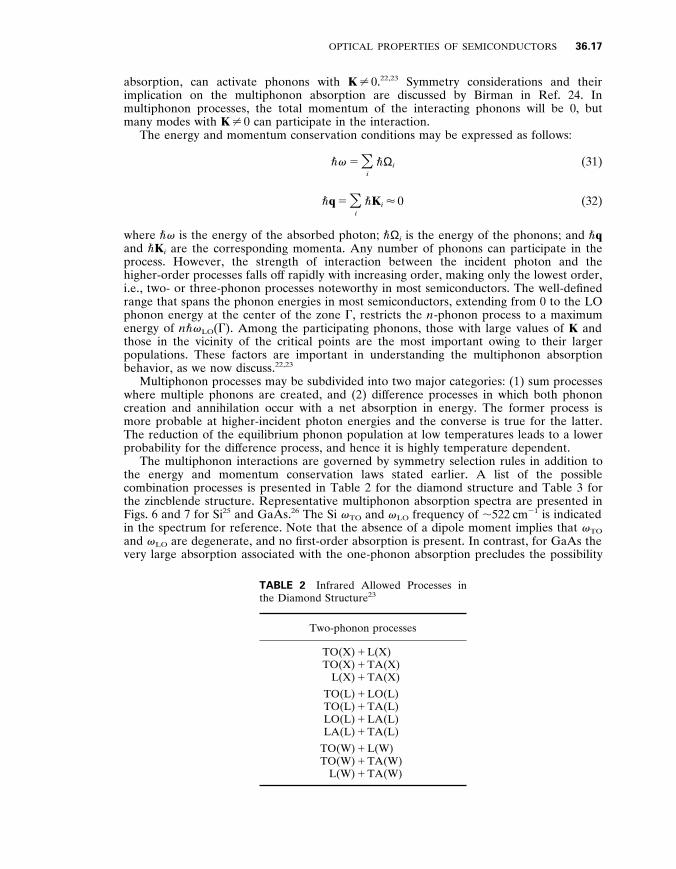
The multiphonon interactions are governed by symmetry selection rules in addition to the energy and momentum conservation laws stated earlier . A list of the possible combination processes is presented in Table 2 for the diamond structure and Table 3 for the zincblende structure . Representative multiphonon absorption spectra are presented in Figs . 6 and 7 for Si 2 5 and GaAs . 2 6 The Si v T O and v L O frequency of , 522 cm 2 1 is indicated in the spectrum for reference . Note that the absence of a dipole moment implies that v T O and v L O are degenerate , and no first-order absorption is present . In contrast , for GaAs the very large absorption associated with the one-phonon absorption precludes the possibility
TABLE 2 Infrared Allowed Processes in the Diamond Structure 2 3
Two-phonon processes
TO(X) 1 L(X) TO(X) 1 TA(X)
L(X) 1 TA(X)
TO(L) 1 LO(L) TO(L) 1 TA(L) LO(L) 1 LA(L) LA(L) 1 TA(L)
TO(W) 1 L(W) TO(W) 1 TA(W)
L(W) 1 TA(W)
36 .18 OPTICAL AND PHYSICAL PROPERTIES OF MATERIALS
TABLE 3 Infrared Allowed Processes in the Zincblende Structure 2 3
Two-phonon processes
2LO( G ) , LO( G ) 1 TO( G ) , 2TO( G ) 2TO(X) , TO(X) 1 LO(X) , TO(X) 1 LA(X) , TO(X) 1 TA(X) LO(X) 1 LA(X) , LO(X) 1 TA(X) LA(X) 1 TA(X) 2TA(X) 2TO(L) , TO(L) 1 LO(L) , TO(L) 1 LA(L) , TO(L) 1 TA(L) 2LO(L) , LO(L) 1 LA(L) , LO(L) 1 TA(L) 2LA(L) , LA(L) 1 TA(L) 2TA(L) TO 1 (W) 1 LO(W) , TO 1 (W) 1 LA(W) TO 2 (W) 1 LO(W) , TO 2 (W) 1 LA(W) LO(W) 1 LA(W) , LO(W) 1 TA 1 (W) , LO(W) 1 TA 2 (W) LA(W) 1 TA 1 (W) , LA(W) 1 TA 2 (W)
of obtaining meaningful multiphonon absorption data in the reststrahlen band that spans the , 269- to 295-cm 2 1 ( , 34- to 37-meV) spectral region . The multiphonon spectra obtained from GaAs are displayed in Figs . 7 a and b . The absorption associated with the multiphonon processes is much smaller than the single-phonon process . However , the rich structure displayed by the spectra is extremely useful in analyzing the lattice dynamics of the material . In addition , in applications such as windows for high-power lasers , even the small absorption levels can lead to paths of catastrophic failure . The multiphonon transmission spectrum of ZnS in the v L O to 2 v L O frequency range is presented in Fig . 8 , and the frequencies and the assignments are presented in Table 4 . 2 7
Impurity - related Vibrational Optical Ef fects . The role of impurities is of primary importance in the control of the electrical characteristics of semiconductors and hence their technological applications . This section outlines the main vibrational features of impurities and the resulting modification of the optical properties of these semiconductors . Impurities can either lead to additional vibrational modes over and beyond that supported
FIGURE 6 Multiphonon absorption of vacuum-grown Si . 2 5

OPTICAL PROPERTIES OF SEMICONDUCTORS 36 .19
FIGURE 7 a Lattice absorption coef ficient of high- resistivity n -type GaAs vs . wavelength from 18 to 28 m m at 20 , 77 , and 293 K . 2 6
FIGURE 7 b Lattice absorption coef ficient of high- resistivity n -type GaAs vs . wavelength from 10 to 18 m m at 77 and 293 K . 2 6
by the unperturbed lattice or they can activate normally inactive vibrational modes . 2 8 The perturbation of the lattice by a substitutional impurity is a change in the mass of one of the constituents and a modification of the bonding forces in its vicinity . If the impurity is much lighter than the host atom it replaces , high-frequency vibrational modes above v L O ( G ) , the maximum frequency supported by the unperturbed lattice , are introduced . These vibrational amplitudes are localized in the vicinity of the impurity and hence are known as local vibrational modes (LVM) . For heavier impurities , the impurity-related vibrations can occur within the phonon band or in the gap between the acoustic and optical bands . These modes are referred to as resonant modes (RM) or gap modes (GM) . 2 8
FIGURE 8 Optical transmittance of chemically vapor-deposited cubic ZnS in the two-phonon ab- sorption regime . 2 7
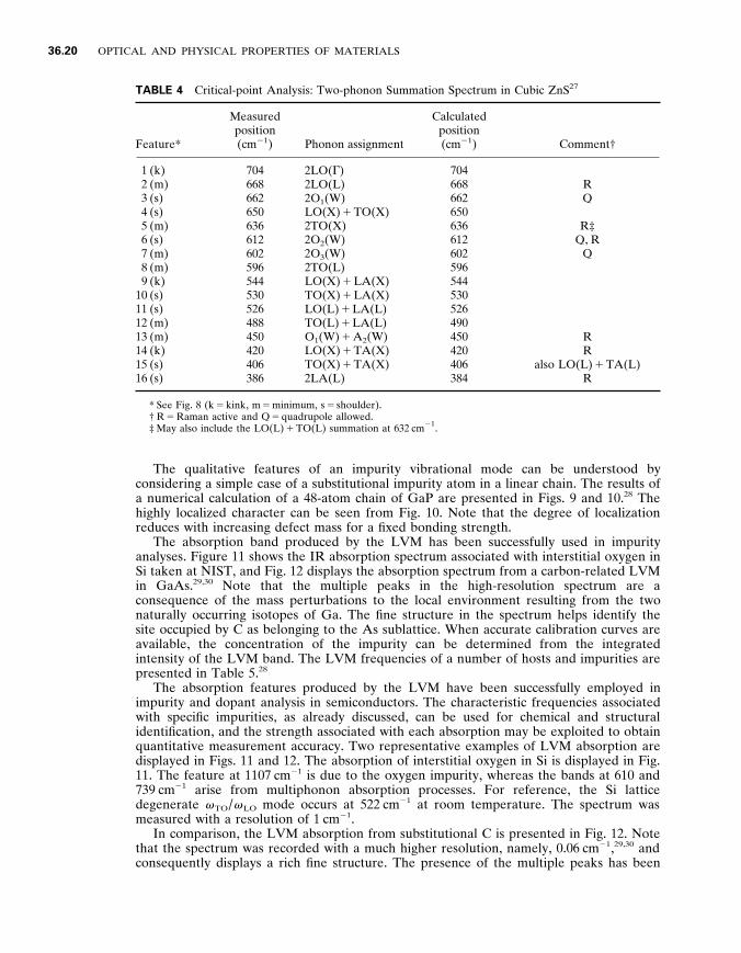
36 .20 OPTICAL AND PHYSICAL PROPERTIES OF MATERIALS
TABLE 4 Critical-point Analysis : Two-phonon Summation Spectrum in Cubic ZnS 2 7
Feature*
Measured position (cm 2 1 ) Phonon assignment
Calculated position (cm 2 1 ) Comment †
1 (k) 2 (m) 3 (s) 4 (s) 5 (m) 6 (s) 7 (m) 8 (m) 9 (k)
704 668 662 650 636 612 602 596 544
2LO( G ) 2LO(L) 2O 1 (W) LO(X) 1 TO(X) 2TO(X) 2O 2 (W) 2O 3 (W) 2TO(L) LO(X) 1 LA(X)
704 668 662 650 636 612 602 596 544
R Q
R ‡ Q , R
Q
10 (s) 11 (s) 12 (m) 13 (m) 14 (k) 15 (s) 16 (s)
530 526 488 450 420 406 386
TO(X) 1 LA(X) LO(L) 1 LA(L) TO(L) 1 LA(L) O 1 (W) 1 A 2 (W) LO(X) 1 TA(X) TO(X) 1 TA(X) 2LA(L)
530 526 490 450 420 406 384
R R
also LO(L) 1 TA(L) R
* See Fig . 8 (k 5 kink , m 5 minimum , s 5 shoulder) . † R 5 Raman active and Q 5 quadrupole allowed . ‡ May also include the LO(L) 1 TO(L) summation at 632 cm 2 1 .
The qualitative features of an impurity vibrational mode can be understood by considering a simple case of a substitutional impurity atom in a linear chain . The results of a numerical calculation of a 48-atom chain of GaP are presented in Figs . 9 and 10 . 2 8 The highly localized character can be seen from Fig . 10 . Note that the degree of localization reduces with increasing defect mass for a fixed bonding strength .
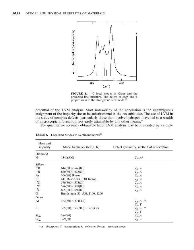
The absorption band produced by the LVM has been successfully used in impurity analyses . Figure 11 shows the IR absorption spectrum associated with interstitial oxygen in Si taken at NIST , and Fig . 12 displays the absorption spectrum from a carbon-related LVM in GaAs . 29 , 30 Note that the multiple peaks in the high-resolution spectrum are a consequence of the mass perturbations to the local environment resulting from the two naturally occurring isotopes of Ga . The fine structure in the spectrum helps identify the site occupied by C as belonging to the As sublattice . When accurate calibration curves are available , the concentration of the impurity can be determined from the integrated intensity of the LVM band . The LVM frequencies of a number of hosts and impurities are presented in Table 5 . 2 8
The absorption features produced by the LVM have been successfully employed in impurity and dopant analysis in semiconductors . The characteristic frequencies associated with specific impurities , as already discussed , can be used for chemical and structural identification , and the strength associated with each absorption may be exploited to obtain quantitative measurement accuracy . Two representative examples of LVM absorption are displayed in Figs . 11 and 12 . The absorption of interstitial oxygen in Si is displayed in Fig . 11 . The feature at 1107 cm 2 1 is due to the oxygen impurity , whereas the bands at 610 and 739 cm 2 1 arise from multiphonon absorption processes . For reference , the Si lattice degenerate v T O / v L O mode occurs at 522 cm 2 1 at room temperature . The spectrum was measured with a resolution of 1 cm 2 1 .
In comparison , the LVM absorption from substitutional C is presented in Fig . 12 . Note that the spectrum was recorded with a much higher resolution , namely , 0 . 06 cm 2 1 , 29 , 30 and consequently displays a rich fine structure . The presence of the multiple peaks has been

OPTICAL PROPERTIES OF SEMICONDUCTORS 36 .21
FIGURE 9 Linear-chain model calculations for GaP . A 48-atom chain is considered . Position along the chain is plotted horizontally and ion displace- ment vertically . Modes 24 and 25 occur on either side of the gap between the acoustic and optic bands . 2 8
FIGURE 10 Eigenvectors for the highest- frequency (localized) mode for three isotopic sub- stitutions on the m 5 31 site . Note the extreme localization for a substituent of mass 5 . 2 8
interpreted to be a consequence of variations in the nearest-neighbor arrangement of the naturally occurring isotopes of the host lattice ions around the impurity . The results of calculation for the vibrational behavior of 1 2 C surrounded by the four possible configura- tions of combinations of 6 9 Ga and 7 1 Ga are displayed in the figure . 3 0 The agreement between theory and measurement is remarkable , which testifies to the power and
FIGURE 11 IR absorption due to interstitial oxygen in Si .
36 .22 OPTICAL AND PHYSICAL PROPERTIES OF MATERIALS
FIGURE 12 1 2 C local modes in GaAs and the predicted fine structure . The height of each line is proportional to the strength of each mode . 3 0
potential of the LVM analysis . Most noteworthy of the conclusion is the unambiguous assignment of the impurity site to be substitutional in the As sublattice . The use of LVM in the study of complex defects , particularly those that involve hydrogen , have led to a wealth of microscopic information , not easily attainable by any other means . 3 1
The quantitative accuracy obtainable from LVM analysis may be illustrated by a simple
TABLE 5 Localized Modes in Semiconductors 2 8
Host and impurity Mode frequency (temp . K) Defect symmetry , method of observation
Diamond N 1340(300) T d , A *
Silicon 1 0 B 1 1 B As P 1 4 C 1 3 C 1 2 C O
644(300) , 646(80) 620(300) , 622(80) 366(80) Reson . 441 Reson , 491(80) Reson . 570(300) , 573(80) 586(300) , 589(80) 605(300) , 680(80) Bands near 30 , 500 , 1100 , 1200
T d , A T d , A T d , A T d , A T d , A T d , A T d , A
GaAs Al
P
Si G a Si A s
362(80) , 371(4 . 2)
355(80) , 353(300) , 363(4 . 2)
384(80) 399(80)
T d , A , R T d , T T d , A , R T d , T T d , A T d , A
* A—absorption : T—transmission ; R—reflection Reson . —resonant mode .

OPTICAL PROPERTIES OF SEMICONDUCTORS 36 .23
FIGURE 13 The absorption coef ficient dependence on the concentration of interstitial oxygen in Si . 3 3
harmonic model calculation . In such an approximation , the total integrated absorption over the entire band may be expressed as : 3 2
E a d v 5 2 π 2 N h 2
h m imp c (33)
where N is the volume density of the impurity and h and m imp are the charge and mass of the impurity ion ; c is the velocity of light . h is an empirically derived parameter that is specific to each center , i . e ., a specific impurity at a specific lattice location . Once calibration curves are established , measurement of the intensity of absorption can be used to determine N . Figure 13 displays a calibration used to establish the density of interstitial oxygen . 3 3 Such analyses are routinely used in various segments of the electronic industry for materials characterization .
The ef fect of the impurities can alter the optical behavior in an indirect fashion as well . The presence of the impurity destroys translational symmetry in its vicinity and hence can lead to relaxation of the wave-vector conservation condition presented earlier in Eq . (33) . Hence , the entire acoustic and optical band of phonons can be activated , leading to absorption bands that extend from zero frequency to the maximum v L O ( G ) . The spectral distribution of the absorption will depend on the phonon density-of-states modulated by the ef fect of the induced dipole moment . 2 8 The latter is a consequence of the perturbation of the charge distribution by the impurity . The perturbation due to defects may be viewed in a qualitatively similar fashion . For instance , a vacancy may be described as an impurity with zero mass .
Interband Absorption Near the Fundamental Edge . The fundamental absorption edge is one of
the most striking features of the absorption spectrum of a semiconductor . Within a small fraction of an electron-volt at an energy about equal to the energy gap E g of the material , the semiconductor changes from being practically transparent to completely opaque—the absorption coef ficient changing by a factor of 10 4 or more . This increased absorption is caused by transitions of electrons from the valence band to the conduction band . This

36 .24 OPTICAL AND PHYSICAL PROPERTIES OF MATERIALS
FIGURE 14 The transmission of CdS , InP , Si , Ge , GaAs , GaP , GaSb , InAs , InSb , PbTe , and PbS . 3 4
characteristic optical property is clearly illustrated in Fig . 14 , which shows the transmission versus wavelength for a number of major semiconductors . 3 4 At the lower wavelengths , the transmission approaches zero which defines a cut-of f wavelength l c , for each material . For example , l c < 7 . 1 m m for InSb ; l c < 4 . 2 m m , PbTe ; l c < 3 . 5 m m , InAs ; l c < 1 . 8 m m , GaSb and Ge ; l c < 1 m m , Si ; and l c < 0 . 7 m m for CdS . At much longer wavelengths than the edge at l c , lattice and free-carrier absorption become appreciable and the transmission drops . Studies of the fundamental absorption edge thus give values for the energy gap and information about the states just above the edge in the conduction band and below it in the valence band . Properties of these states are important to know since they are responsible for electrical conduction . Details of the band structure near the band extrema can be determined from the position and shape of the absorption edge and from its temperature , magnetic field , pressure , impurity concentration , and other parameters dependence . Finally , this fundamental gap region is important because usually it is only near the energy gap that phenomena such as excitons (both free and bound) , electron-hole drops , donor-acceptor pairs , etc ., are seen .
Interband transitions near the fundamental absorption edge are classified as (1) direct or vertical or (2) indirect or nonvertical . The momentum of light ( " k 5 " n v / c ) is negligible compared to the momentum of a k -vector state at the edge of the Brillouin zone . Thus , because of momentum conservation , electrons with a given wave vector in a band can only make transitions to states in a higher band having essentially the same wave vector . Such transitions are called vertical transitions . A nonvertical transition can take place , but only with the assistance of phonons or other entities which help preserve momentum .
Direct Transitions . The interband absorption coef ficient depends upon the band structure and photon energy " v . Use of quantum mechanics and , in particular , time-dependent perturbation theory , becomes necessary . 3 5 Direct transitions (with ap- proximate conservation of the electron wave vector) can then be separated into ‘‘allowed’’ and ‘‘forbidden’’ transitions , depending on whether the dipole matrix element which determines the transition probability between the bands or the absorption coef ficient is finite or vanishes in first approximation . For a nonzero momentum matrix element , a simple model gives for allowed direction transitions
a A D 5 C A D ( " v 2 E g ) 1/2 (34)
and for forbidden direct transitions with a zero dipole matrix element
a F D 5 C F D ( " v 2 E g ) 3/2 (35)
Both coef ficients involve constants , valence- and conduction-band ef fective masses , and matrix elements , and only a slight dependence on photon energy . The absorption strengths of direct-gap semiconductors are related to their density of states and the momentum

OPTICAL PROPERTIES OF SEMICONDUCTORS 36 .25
FIGURE 15 Theoretical fit to the experimental absorption edge of InSb at , 5 K . 3 6 FIGURE 16 Absorption edge of GaAs at room
temperature . 3 8
matrix element that couples the bands of interest . Semiconductors such as AlAs , AlP , GaAs , InSb , CdS , ZnTe , and others have allowed direct transitions ; many complex oxides such as Cu 2 O , SiO 2 , rutile , and others have forbidden direct absorption .
Figure 15 shows the spectral variation of the absorption coef ficient for pure InSb at a temperature of 5 K compared to various theoretical predictions . 3 6 We note the extremely sharp absorption edge which is fit best by the ( " v 2 E g ) 1/2 dependence near the edge . However , a big deviation from the experimental data occurs at higher photon energies . Consideration of two more details allows a better fit : (1) use of a more complicated band model from Kane 3 7 which predicts a more rapidly increasing density of states than for the simple bands , and (2) taking into account a decrease in the optical matrix element at the higher photon energies because of the k -dependence of the wave functions . The calculated curves in Fig . 4 were arbitrarily shifted so that they look like a better fit than they are . The actual calculated absorption is a factor of about 15 too low at high energies . This discrepancy was attributed to the neglect of exciton ef fects which can greatly af fect the absorption as discussed later .
Figure 16 shows the absorption behavior of GaAs at room temperature compared with calculations based on Kane’s theory . 3 8 Below about 10 3 cm 2 1 , the absorption decreases much more slowly than predicted and absorption is even present for energies below E g . In practice , there seems to exist an exponentially increasing absorption edge rule (called Urbach’s rule) in most direct transition materials which is found to correlate reasonably well with transitions involving band tails . These band tails seem to be related to doping ef fects and phonon-assisted transitions .
Indirect Transitions . Semiconductors such as GaP , Ge , and Si have indirect gaps where the maximum valence-band energy and minimum conduction-band energy do not occur at the same k value . In this case , the electron cannot make a direct transition from the top of the valence band to the bottom of the conduction band because this would violate conservation of momentum . Such a transition can still take place but as a two-step process requiring the cooperation of another particle and which can then be described by second-order perturbation theory . The particle most frequently involved is an intervalley phonon of energy " Ω K which can be either generated or absorbed in the transition . (In some cases , elastic scattering processes due to impurity atoms or dislocations must be considered ; they are less frequent than the phonon interactions . ) The photon supplies the needed energy , while the phonon supplies the required momentum . The transition probability depends not only on the density of states and the electron-phonon matrix

36 .26 OPTICAL AND PHYSICAL PROPERTIES OF MATERIALS
elements as in the direct case , but also on the electron-phonon interaction which is temperature dependent .
Calculations of the indirect-gap absorption coef ficient give for the allowed indirect transitions
a A I 5 C (abs) AI ( " v 1 " Ω q 2 E g ) 2 1 C (em)
AI ( " v 2 " Ω q 2 E g ) 2 (36)
and for the forbidden indirect transitions
a F I 5 C (abs) FI ( " v 1 " Ω q 2 E g ) 3 1 C (em)
FI ( " v 2 " Ω q 2 E g ) 3 (37)
where the superscripts (abs) and (em) refer to phonon absorption and emission , respectively . These expressions are only nonzero when the quantities in parentheses are positive , i . e ., when " v Ú " Ω q . E g . We note that the phonon energies are usually small ( # 0 . 05 eV) compared to the photon energy of about 1 eV and thus for the case of allowed indirect transitions with phonon absorption
a A I < C (abs) AI ( " v 2 E g ) 2 (38)
Thus the absorption increases as the second power of ( " v 2 E g ) , much faster than the half-power dependence of the direct transition as seen in Eq . (34) .
Figure 17 shows the variation of the absorption coef ficient of GaP with photon energy at room temperature near the indirect edge . 3 9 A reasonable fit to the experimental data of Spitzer et al . 4 0 is obtained indicating that , for GaP , allowed indirect transitions dominate . Further complications arise because there can be more than one type of phonon emitted or absorbed in the absorption process . Transverse acoustic (TA) , longitudinal acoustic (LA) , transverse optic (TO) , and longitudinal optic (LO) phonons can be involved as shown in the absorption edge data of GaP , as seen in Fig . 18 . 4 1 The phonon energies deduced from these types of experimental absorption edge studies agree with those found from neutron scattering .
FIGURE 17 Comparison of the experimental data at room temperature for the absorption edge of GaP with the theory for an indirect edge . 3 9
FIGURE 18 Absorption spectra at the edge of GaP , showing thresholds associated with the emis- sion of each of several dif ferent phonons . 4 1

OPTICAL PROPERTIES OF SEMICONDUCTORS 36 .27
FIGURE 19 ( a ) a vs . " v for Ge ; ( b ) the analysis of the 300 K experimental data . 4 2
Both indirect and direct absorption edge data for Ge are shown in Fig . 19 while the analysis of the 300 K data is plotted in part b . 4 2 At the lowest energies , a rises due to the onset of indirect absorption as seen by the a 1/2 dependence on photon energy . At higher energies , a sharper rise is found where direct transitions occur at the zone center and an a 2
dependence on energy is then seen . Note the large shifts of E g with temperature for both the direct and indirect gaps . Also , the direct-gap absorption is much stronger than that of the indirect-gap absorption .
Excitons . Among the various optical properties of semiconductors , the subject of excitons has one of the dominant places because of their remarkable and diverse properties . Studies of exciton properties represent one of the most important aspects of scientific research among various solid-state properties . According to Cho , 4 3 there are a number of reasons for this : (1) excitonic phenomena are quite common to all the nonmetallic solids—semiconductors , ionic crystals , rare gas crystals , molecular crystals , etc . ; (2) the optical spectra often consist of sharp structure , which allows a detailed theoretical analysis ; (3) theories are not so simple as to be understood by a simple application of atomic theory or the Bloch band scheme , but still can be represented by a quasi-hydrogenlike level scheme ; (4) sample quality and experimental techniques have continually been improved with subsequent experiments proving existing theories and giving rise to new ones ; and (5) the exciton is an elementary excitation of nonmetallic solids , a quantum of electronic polarization . It has a two-particle (electron and hole) nature having many degrees of freedom , and along with the variety of energy-band structures , this leads to a lot of dif ferent properties from material to material or from experiment to experiment . Table 6 gives a definition of the major types of excitons in a glossary obtained from Hayes and Stoneham . 4 4 Many examples exist in the literature involving work on excitons in semiconductors to understand their nature and to determine their properties . Besides the references cited in this chapter , the authors refer the reader to the more detailed work presented in Refs . 45 and 46 .
An electron , excited from the valence band to a higher energy state , can still be bound by the Coulomb attraction to the hole that the electron leaves in the valence band . This neutral bound-electron hole pair is called an exciton which can move throughout the crystal . Excitons are most easily observed at energies just below E g using optical absorption or photoluminescence measurements . There are two models used for describing excitons in solids , named after Frenkel and Wannier . In a solid consisting of weakly interacting atoms , Frenkel considered excitons as described by excitations of a single atom or molecule . 4 7 An excited electron describes an orbit of atomic dimensions around an

36 .28 OPTICAL AND PHYSICAL PROPERTIES OF MATERIALS
TABLE 6 A Glossary of the Main Species of Excitons 4 4
Exciton In essence , an electron and hole moving with a correlated motion as an electron-hole pair .
Wannier exciton Electron and hole both move in extended orbits ; energy levels related to hydrogen-atom levels by scaling , using ef fective masses and dielectric constant ; occurs in covalent solids such as silicon
Frenkel exciton Electron and hole both move in compact orbits , usually essentially localized on adjacent ions ; seen in ionic solids , such as KCl , in absorption
Self-trapped exciton One or both carriers localized by the lattice distortion they cause ; observed in ionic solids , such as KCl , in emission
Bound exciton Only a useful idea when a defect merely prevents translational motion of an exciton and does not otherwise cause significant perturbation
Core exciton Lowest-energy electronic excitation from a core state , leaving an unoccupied core orbital (e . g ., the 1 s level of a heavy atom) and an electron in the conduction band whose motion is correlated with that of the core hole
Excitonic molecule Complex involving two holes and two electrons
Multiple bound excitons Complex of many holes and a similar number of electrons , apparently localized near impurities ; some controversy exists , but up to six pairs of localized carriers have been suggested
Exciton gas High concentration of electrons and holes in which each electron remains strongly associated with one of the holes (as insulating phase)
Electron-hole drops High concentration of electrons and holes in which the motions are plasmalike (a metallic phase) , not strongly correlated as in excitons
atom with a vacant valence state . The empty valence state acts as a mobile hole since the excitation can move from one atom to another . These tightly bound excitons are similar to an ordinary excited state of the atom , except that the excitation can propagate through the solid . The radius of the Frenkel exciton is on the order of the lattice constant . Frenkel excitons are useful to describe optical properties of solids like alkali halides and organic phosphors .
Wannier (or also called Mott-Wannier) excitons are also electrons and holes bound by Coulomb attraction . 48 , 49 In contrast to the Frenkel exciton , the electron and hole are separated by many lattice spacings producing a weakly bound exciton which is remarkably similar to a hydrogen-atom-like system . Since the electron and hole are , on the average , several unit cells apart , their Coulomb interaction is screened by the average macroscopic dielectric constant e , and electron and hole ef fective masses can be used . Their potential energy 2 e 2 / e r is just that of the hydrogen atom (except for e ) . The energy binding of the free exciton (relative to a free electron and free hole) is then given by the hydrogen-atom- like discrete energy levels plus a kinetic energy term due to the motion of the exciton :
E e x 5 R y
n 2 2 " 2 k 2
2( m * e 1 m * h ) (39)
R y 5 S m r
e 2 D S e 4
2 " 2 D 5 S m r
m H e 2 D E H (40)
where
m r 5 S 1 m * e
1 1
m * h D 2 1
(41)
OPTICAL PROPERTIES OF SEMICONDUCTORS 36 .29
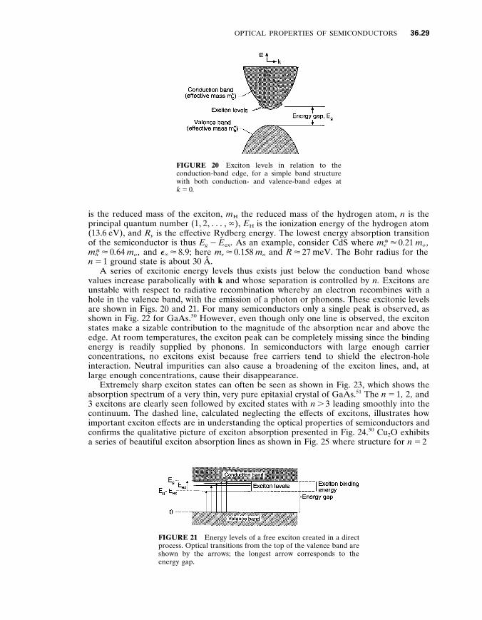
FIGURE 20 Exciton levels in relation to the conduction-band edge , for a simple band structure with both conduction- and valence-band edges at k 5 0 .
is the reduced mass of the exciton , m H the reduced mass of the hydrogen atom , n is the principal quantum number (1 , 2 , . . . , ) , E H is the ionization energy of the hydrogen atom (13 . 6 eV) , and R y is the ef fective Rydberg energy . The lowest energy absorption transition of the semiconductor is thus E g 2 E e x . As an example , consider CdS where m e * < 0 . 21 m o , m h * < 0 . 64 m o , and e < 8 . 9 ; here m r < 0 . 158 m o and R < 27 meV . The Bohr radius for the n 5 1 ground state is about 30 Å .
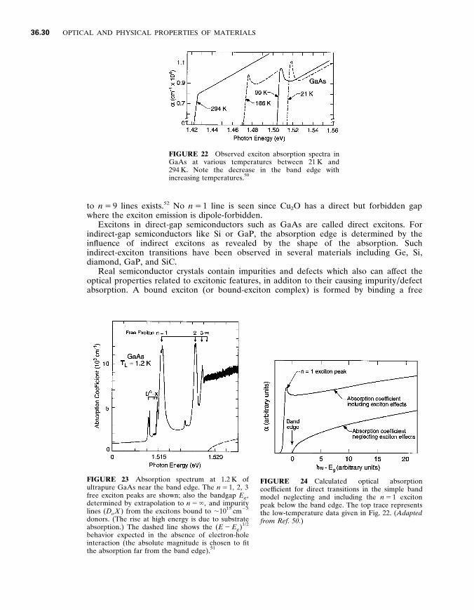
A series of excitonic energy levels thus exists just below the conduction band whose values increase parabolically with k and whose separation is controlled by n . Excitons are unstable with respect to radiative recombination whereby an electron recombines with a hole in the valence band , with the emission of a photon or phonons . These excitonic levels are shown in Figs . 20 and 21 . For many semiconductors only a single peak is observed , as shown in Fig . 22 for GaAs . 5 0 However , even though only one line is observed , the exciton states make a sizable contribution to the magnitude of the absorption near and above the edge . At room temperatures , the exciton peak can be completely missing since the binding energy is readily supplied by phonons . In semiconductors with large enough carrier concentrations , no excitons exist because free carriers tend to shield the electron-hole interaction . Neutral impurities can also cause a broadening of the exciton lines , and , at large enough concentrations , cause their disappearance .
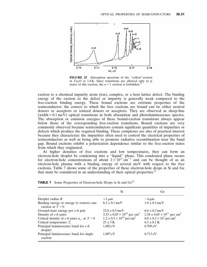
Extremely sharp exciton states can often be seen as shown in Fig . 23 , which shows the absorption spectrum of a very thin , very pure epitaxial crystal of GaAs . 5 1 The n 5 1 , 2 , and 3 excitons are clearly seen followed by excited states with n . 3 leading smoothly into the continuum . The dashed line , calculated neglecting the ef fects of excitons , illustrates how important exciton ef fects are in understanding the optical properties of semiconductors and confirms the qualitative picture of exciton absorption presented in Fig . 24 . 5 0 Cu 2 O exhibits a series of beautiful exciton absorption lines as shown in Fig . 25 where structure for n 5 2
FIGURE 21 Energy levels of a free exciton created in a direct process . Optical transitions from the top of the valence band are shown by the arrows ; the longest arrow corresponds to the energy gap .
36 .30 OPTICAL AND PHYSICAL PROPERTIES OF MATERIALS
FIGURE 22 Observed exciton absorption spectra in GaAs at various temperatures between 21 K and 294 K . Note the decrease in the band edge with increasing temperatures . 5 0
to n 5 9 lines exists . 5 2 No n 5 1 line is seen since Cu 2 O has a direct but forbidden gap where the exciton emission is dipole-forbidden .
Excitons in direct-gap semiconductors such as GaAs are called direct excitons . For indirect-gap semiconductors like Si or GaP , the absorption edge is determined by the influence of indirect excitons as revealed by the shape of the absorption . Such indirect-exciton transitions have been observed in several materials including Ge , Si , diamond , GaP , and SiC .
Real semiconductor crystals contain impurities and defects which also can af fect the optical properties related to excitonic features , in additon to their causing impurity / defect absorption . A bound exciton (or bound-exciton complex) is formed by binding a free
FIGURE 23 Absorption spectrum at 1 . 2 K of ultrapure GaAs near the band edge . The n 5 1 , 2 , 3 free exciton peaks are shown ; also the bandgap E g , determined by extrapolation to n 5 , and impurity lines ( D o X ) from the excitons bound to , 10 1 5 cm 2 3
donors . (The rise at high energy is due to substrate absorption . ) The dashed line shows the ( E 2 E g ) 1/2
behavior expected in the absence of electron-hole interaction (the absolute magnitude is chosen to fit the absorption far from the band edge) . 5 1
FIGURE 24 Calculated optical absorption coef ficient for direct transitions in the simple band model neglecting and including the n 5 1 exciton peak below the band edge . The top trace represents the low-temperature data given in Fig . 22 . ( Adapted from Ref . 5 0 . )
OPTICAL PROPERTIES OF SEMICONDUCTORS 36 .31
FIGURE 25 Absorption spectrum of the ‘‘yellow’’exciton in Cu 2 O at 1 . 8 K . Since transitions are allowed only to p states of this exciton , the n 5 1 exciton is forbidden . 5 2
exciton to a chemical impurity atom (ion) , complex , or a host lattice defect . The binding energy of the exciton to the defect or impurity is generally weak compared to the free-exciton binding energy . These bound excitons are extrinsic properties of the semiconductor ; the centers to which the free excitons are bound can be either neutral donors or acceptors or ionized donors or acceptors . They are observed as sharp-line (width < 0 . 1 meV) optical transitions in both absorption and photoluminescence spectra . The absorption or emission energies of these bound-exciton transitions always appear below those of the corresponding free-exciton transitions . Bound excitons are very commonly observed because semiconductors contain significant quantities of impurities or defects which produce the required binding . These complexes are also of practical interest because they characterize the impurities often used to control the electrical properties of semiconductors as well as being able to promote radiative recombination near the band gap . Bound excitons exhibit a polarization dependence similar to the free-exciton states from which they originated .
At higher densities of free excitons and low temperatures , they can form an electron-hole droplet by condensing into a ‘‘liquid’’ phase . This condensed phase occurs for electron-hole concentrations of about 2 3 10 1 7 cm 2 3 and can be thought of as an electron-hole plasma with a binding energy of several meV with respect to the free excitons . Table 7 shows some of the properties of these electron-hole drops in Si and Ge that must be considered in an understanding of their optical properties . 5 3
TABLE 7 Some Properties of Electron-hole Drops in Si and Ge 5 3
Si Ge
Droplet radius R , 1 m m , 4 m m Binding energy or energy to remove one
exciton at T 5 0 8 . 2 Ú 0 . 1 meV 1 . 8 Ú 0 . 2 meV
Ground-state energy per e - h pair 22 . 8 Ú 0 . 5 meV 6 . 0 Ú 0 . 2 meV Density of e - h pairs 3 . 33 Ú 0 . 05 3 10 1 8 per cm 3 2 . 38 Ú 0 . 05 3 10 1 7 per cm 3
Critical density of e - h pairs n c , at T 5 0 1 . 2 Ú 0 . 5 3 10 1 8 per cm 3 0 . 8 Ú 0 . 2 3 10 7 per cm 3
Critical temperature T c 25 Ú 5 K 6 . 5 Ú 0 . 1 K Principal luminescence band for e - h
droplet 1 . 082 eV 0 . 709 eV
Principal luminescence band for single exciton
1 . 097 eV 0 . 713 eV

36 .32 OPTICAL AND PHYSICAL PROPERTIES OF MATERIALS
Polarizations . Interesting optical ef fects arise when one considers explicitly the influence of longitudinal and transverse optical phonons on a transverse electromagnetic wave propagating through the semiconductor . This influence can be taken into account via the dielectric function of the medium . Dispersion curves that arise do not conform either to the photon or to the phonon . The coupling between the photon and phonon becomes so strong that neither can continue to be regarded as an independent elementary excitation , but as a photon-phonon mixture! This mixture can be regarded as a single quantity which can be interpreted as a new elementary excitation , the polariton . 5 4 Similar couplings exist between an exciton and the photon . It is an important consideration for interpreting some optical processes involving Raman and luminescence measurements .
High - Energy Transitions Abo y e the Fundamental Edge . The optical properties of most semiconductors have been thoroughly investigated throughout the visible and ultraviolet regions where transitions above the fundamental gap energy give rise to properties strongly dependent upon photon energy . This regime is dominated by optical absorption and reflection of a photon arising from both valence and core electron transitions from the ground state of the system into various bound , autoionizing , continuum , or other excited states . The sum of all excitations—both bound (nonionizing) and ionizing—gives the total absorption coef ficient and the complex dielectric constant at each photon energy h … . Photoemission or photoelectron spectroscopy measurements in this high-energy regime provide an alternative to ultraviolet spectroscopy for providing detailed information on the semiconductor . (See the electromagnetic spectrum in Fig . 1 in the Introduction for a reminder that photoemission measurements overlap UV measurements . ) Electrons may be ejected from the semiconductor by high-energy photons as shown in Fig . 26 . 5 5 Their kinetic energies are measured and analyzed to obtain information about the initial electron states . Ionizing excitations involve electron excitations into unbound states above the vacuum level . These excitations result in photoemission as depicted for the two valence bands and the core level shown . For photoemission involving one-electron excitations (usually dominant) , binding energies E B of valence and core levels are given directly by the measured kinetic energies E (from N ( E ) in the figure and energy conservation) :
E B 5 h … 2 E 2 f (42)
FIGURE 26 A schematic energy-level diagram showing photoemission from the valence bands and a core level in a solid . 5 5

OPTICAL PROPERTIES OF SEMICONDUCTORS 36 .33
FIGURE 27 The spectral dependence of the re- flectance R , the real and imaginary parts of the dielectric constant e 1 and e 2 , and the energy-loss function 2 Im ( e
2 1 ) for InSb . 56 , 61
Here f is the work function (usually about 2 to 5 eV for most clean solids) which is known or easily measured . X-ray photoemission spectroscopy (XPS) is usually used to study core states and ultraviolet photoemission spectroscopy (UPS) to study valence-band states . Photoemission techniques are also used for the study of surface states . Synchrotron radiation provides an intense source of light over a large spectral region . By measuring the angular distribution of the emitted UPS electrons , a direct determination of the E versus k relation for the valence band of GaAs can be made .
There are several regions of importance that must be considered in describing the optical properties of this high-energy region . Figure 27 shows the regions for InSb that are representative of the results for other semiconductors . 5 6 InSb is a narrow gap material with a direct band gap of 0 . 17 eV at room temperature , so what is shown is at much greater energies than E g . Sharp structure associated with transitions from the valence band to higher levels in the conduction band characterize the first region that extends to about 8 to 10 eV . That this behavior is characteristic of other III-V compounds can be seen in Fig . 28 which shows the reflectance for InAs , GaAs , and GaP as well as InSb . 5 7 To show how this type of optical spectra can be interpreted in terms of the materials energy band structure , consider Fig . 29 which shows the spectral features of e 2 for Ge in a and the calculated energy bands for Ge in b . 58 , 59 Electronic transitions can take place between filled and empty bands subject to conservation of energy and wave vector . The initial and final electron wave vectors are essentially equal , and only vertical transitions between points separated in energy by " v 5 E c ( k ) 2 E … ( k ) are allowed .
The intensity of the absorption is proportional to the number of initial and final states and usually peaks when the conduction and valence bands are parallel in k -space . This condition is expressed by
= k [ E c ( k ) 2 E … ( k )] 5 0 (43)
Places in k -space where this is true are called critical points or Van Hove singularities .

36 .3
4 OPTICAL AND PHYSICAL PROPERTIES OF MATERIALSFIGURE 28 Reflectance of several III – V com- pounds at room temperature . For clarity , the spectra are of fset along the y axis by the amounts shown in brackets . 5 7
FIGURE 29 ( a ) Spectral features of e 2 for Ge ; ( b ) the calculated pseudopotential energy bands for Ge along some of the principal axes . 58 , 59
The experimental peaks can be sharp as shown in Fig . 29 a because interband transitions are not appreciably broadened by damping and thus the lineshapes are determined by the density of states . Much information is available from the data if a good theory is used . Figure 29 b shows pseudopotential energy-band calculations that show the special points and special lines in the Brillouin zone that give rise to the data shown in a .
The second region in Fig . 27 extends to about 16 eV and shows a rapid decrease of reflectance due to the excitation of collective plasma oscillations of the valence electrons . The behavior in this second ‘‘metallic’’ region is typical of the behavior of certain metals in the ultraviolet . One can think of the valence electrons as being essentially unbound and able to perform collective oscillations . Sharp maxima in the function 2 Im e 2 1 , which describes the energy loss of fast electrons traversing the material , have been frequently associated with the existence of plasma oscillations .
In the third region , the onset of additional optical absorption is indicated by the rise in reflectance . This structure is identified with transitions between filled d bands below the valence band and empty conduction-band states . As shown in Fig . 30 , the structure in region three is present in other III-V compounds , but is absent in Si which does not have a d-band transition in this region . 6 0 Other structure at higher photon energies is observed for Si as shown in Fig . 31 which shows the imaginary part of the dielectric constant of Si from 1 to 1000 eV . 61 , 62 The large peaks on the left are due to excitations of valence electrons , whereas the peaks on the right are caused by excitation of core electrons from L shell states . K shell electrons are excited at energies beyond the right edge of the graph .

OPTICAL PROPERTIES OF SEMICONDUCTORS 36 .35
FIGURE 30 Reflectance of several semiconductors at intermediate energies . Starting from 12 eV the reflectance decreases , representing the exhaustion of bonding 5 antibonding oscillator strength at energies greater than 2 E g . The rise in reflectivity in the 15 – 20 eV range in the Ga and In compounds is caused by excitation of electrons from Ga cores (3d states) or In cores (4d states) . The ordinate should be multiplied by 2 for InSb , 1 for InAs , 1 / 2 for GaAs , 1 / 4 for GaP , and 1 / 10 for Si . 6 0
FIGURE 31 Imaginary part of the dielectric func- tion for Si from 1 to 1000 eV . 2 [From reflectivity measurements of H . R . Philipp and H . Ehrenreich , Ref . 61 , out to 20 eV and from transmission mea- surements of C . Gahwiller and F . C . Brown , Ref . 62 , from 40 to 200 eV . ]
Free Carriers Plasmons . Semiconductors , in addition to a crystal lattice that may be ionic , may
contain free charges as well . The free-carrier contribution to the dielectric function is given by Maxwell’s equation in
CGS units
e f c ( v ) 5 2 i 4 π s
v (44)
The task of establishing the functional form of e ( v ) hence reduces to one of determining the conductivity at the appropriate optical frequencies .
The response of a charge to an externally applied field may be described by classical methods , assuming a damping or resistive force to the charge that is proportional to the velocity of the charge . This simplification is known as the Drude approximation , 6 3 and it leads to the following relationship :
s 5 Ne 2 τ m *
1 (1 2 i v τ )
(45)

36 .36 OPTICAL AND PHYSICAL PROPERTIES OF MATERIALS
and is related to the dc conductivity by the relationship :
s (0) 5 Ne 2 τ / m * (46)
where N is the free carrier density and 1 / τ is the constant of proportionality for the damping force and τ is a measure of the electron-electron collision time . Now ,
e f c ( v ) 5 2 i v 2
P e
v S v 1 i τ D
(47)
v p is the plasma frequency that describes oscillations of the plasma , i . e ., the delocalized charge cloud
v 2 P 5
4 π Ne 2
m * e
(48)
against the fixed crystal lattice . In an ideal plasma with no damping , the e ( v ) reduces to :
e ( v ) 5 1 2 v 2
p
v 2 (49)
e ( v ) is negative for v , v p , which leads to total reflection and , hence , the term plasma reflectivity .
The behavior of plasma reflection and the relationship to the free-carrier density is illustrated in Fig . 32 using the far-infrared reflection spectrum from a series of PbTe
FIGURE 32 Reflectivity at 81 K and normal incidence of variously doped samples of p-type PbTe , showing the plasma resonance . Hole concentrations : A , 3 . 5 3 10 1 8 cm 2 3 ; B , 5 . 7 3 10 1 8 cm 2 3 ; C , 1 . 5 3 10 1 9 ; D , 4 . 8 3 10 1 9 cm 2 3 . 6 4
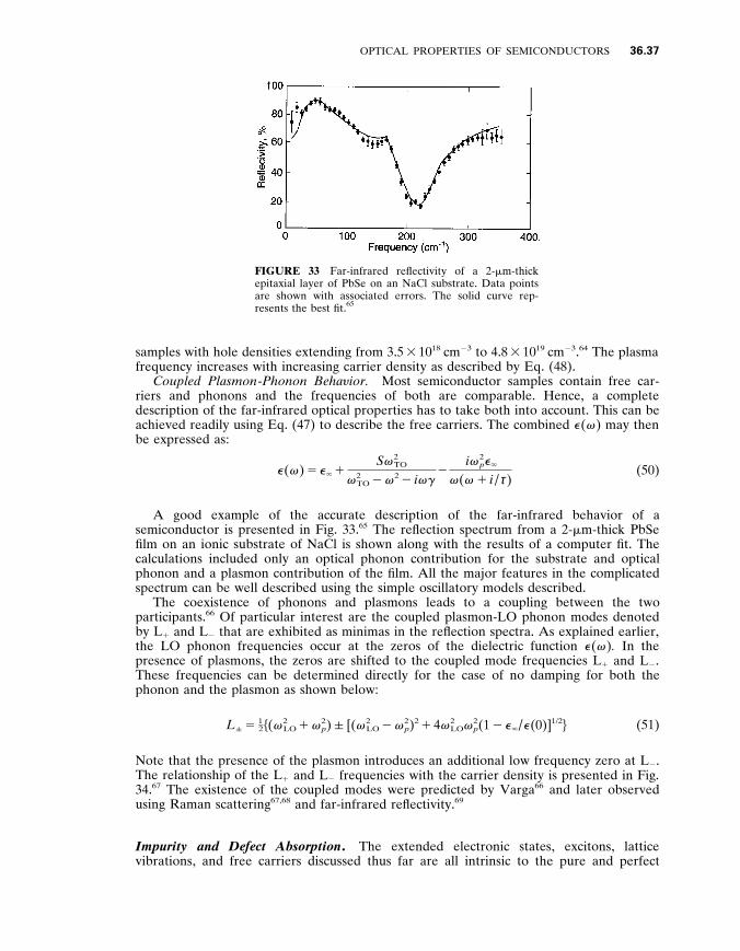
OPTICAL PROPERTIES OF SEMICONDUCTORS 36 .37
FIGURE 33 Far-infrared reflectivity of a 2- m m-thick epitaxial layer of PbSe on an NaCl substrate . Data points are shown with associated errors . The solid curve rep- resents the best fit . 6 5
samples with hole densities extending from 3 . 5 3 10 1 8 cm 2 3 to 4 . 8 3 10 1 9 cm 2 3 . 6 4 The plasma frequency increases with increasing carrier density as described by Eq . (48) .
Coupled Plasmon - Phonon Beha y ior . Most semiconductor samples contain free car- riers and phonons and the frequencies of both are comparable . Hence , a complete description of the far-infrared optical properties has to take both into account . This can be achieved readily using Eq . (47) to describe the free carriers . The combined e ( v ) may then be expressed as :
e ( v ) 5 e 1 S v 2
TO
v 2 TO 2 v 2 2 i v g
2 i v 2
p e
v ( v 1 i / τ ) (50)
A good example of the accurate description of the far-infrared behavior of a semiconductor is presented in Fig . 33 . 6 5 The reflection spectrum from a 2- m m-thick PbSe film on an ionic substrate of NaCl is shown along with the results of a computer fit . The calculations included only an optical phonon contribution for the substrate and optical phonon and a plasmon contribution of the film . All the major features in the complicated spectrum can be well described using the simple oscillatory models described .
The coexistence of phonons and plasmons leads to a coupling between the two participants . 6 6 Of particular interest are the coupled plasmon-LO phonon modes denoted by L 1 and L 2 that are exhibited as minimas in the reflection spectra . As explained earlier , the LO phonon frequencies occur at the zeros of the dielectric function e ( v ) . In the presence of plasmons , the zeros are shifted to the coupled mode frequencies L 1 and L 2 . These frequencies can be determined directly for the case of no damping for both the phonon and the plasmon as shown below :
L Ú 5 1 – 2 h ( v 2 LO 1 v 2
p ) Ú [( v 2 LO 2 v 2
p ) 2 1 4 v 2 LO v 2
p (1 2 e / e (0)] 1/2 j (51)
Note that the presence of the plasmon introduces an additional low frequency zero at L 2 . The relationship of the L 1 and L 2 frequencies with the carrier density is presented in Fig . 34 . 6 7 The existence of the coupled modes were predicted by Varga 6 6 and later observed using Raman scattering 67 , 68 and far-infrared reflectivity . 6 9
Impurity and Defect Absorption . The extended electronic states , excitons , lattice vibrations , and free carriers discussed thus far are all intrinsic to the pure and perfect

36 .38 OPTICAL AND PHYSICAL PROPERTIES OF MATERIALS
FIGURE 34 The solid curves labeled L 1 and L 2 give the calculated frequencies of the coupled longitudinal plasmon-phonon modes and the measured frequencies are denoted by the open circles . 6 8
crystal . In practice , real-life specimens contain imperfections and impurities . The charac- teristic optical properties associated with impurities and defects are the subject of discussion in this section . Two representative examples of the most widely observed ef fects , namely , shallow levels and deep levels in the forbidden gap , are considered in the following discussion .
Some of the ef fects due to impurities are considered in other parts of this chapter : impurity-related vibrational ef fects were considered under ‘‘Lattice’’ ; excitons bound to impurity states were discussed under ‘‘Excitons’’ ; and impurity-related ef fects in magneto- optical behavior are dealt with under ‘‘Magnetic-Optical Properties . ’’ In addition to these ef fects , optical absorption due to electronic transitions between impurity-related electronic levels may also be observed in semiconductors .
The presence of impurities in a semiconductor matrix leads to both a perturbation of the intrinsic electronic quantum states and the introduction of new states , particularly in the forbidden energy gap . The major classes of electronic levels are the shallow levels that form the acceptor and donor states and lie close to the valence and conduction band extremes , respectively , and those that occur deep in the forbidden gap . The former are well known and are critical in controlling the electrical behavior of the crystal , and the latter are less well known but are , nevertheless , important in determining the subband gap optical behavior .
Direct transitions from the shallow levels to the closest band extrema can be observed in the far-infrared transmission spectra of many semiconductors . An elegant example of this property is illustrated with the spectrum obtained from a high-purity Si wafer 7 0 as displayed in Fig . 35 . Sharp , well-resolved absorption features from electronic transitions due to B , P , As , and Al are present , as are additional features , perhaps from unidentified impurities . Note that both acceptors and donor bands are observable due to the highly nonequilibrium state in which the specimen was maintained through the use of intense photoexcitation .
Electronic transitions from impurity- and defect-related levels deep in the forbidden gap can significantly alter the subband gap behavior . One of the best known examples of

OPTICAL PROPERTIES OF SEMICONDUCTORS 36 .39
FIGURE 35 Total impurity spectrum of a 265- Ω -cm n -type Si sample obtained by the simultaneous illumination method . The input power to the illumination source was about 50 W . 7 0
this is the native defect level known as EL2 in GaAs . The level occurs 0 . 75 eV below the conduction-band extremum , and when present , it can completely dominate the subband gap absorption . The absorption spectrum recorded from a GaAs sample containing EL2 is presented in Fig . 36 . 7 1 The onset of the absorption at 0 . 75 eV is due to transitions to the conduction-band extremum at the direct gap , and the features at 1 . 2 and 1 . 4 eV are due to transitions to higher-lying extrema . 7 1 The figure also shows two spectra that exhibit the well-known photoquenching ef fect associated with EL2 . When the specimen is subjected to intense white light radiation , the EL2 absorption is quenched , leaving only the band-to- band transitions with an onset at E g which occurs at , 1 . 5 eV at 10 K .
Optical measurements of shallow impurities in semiconductors have been carried out by absorption (transmission) and photoconductivity techniques . The photoconductivity method is a particularly powerful tool for studying the properties of shallow impurity states , especially in samples which are too pure or too thin for precise absorption
FIGURE 36 EL2 optical absorption spectra re- corded at 10 K in the same undoped semi-insulating GaAs material . Curve a : after cooling in the dark ; curves b and c : after white light illumination for 1 and 10 min , respectively . 7 1
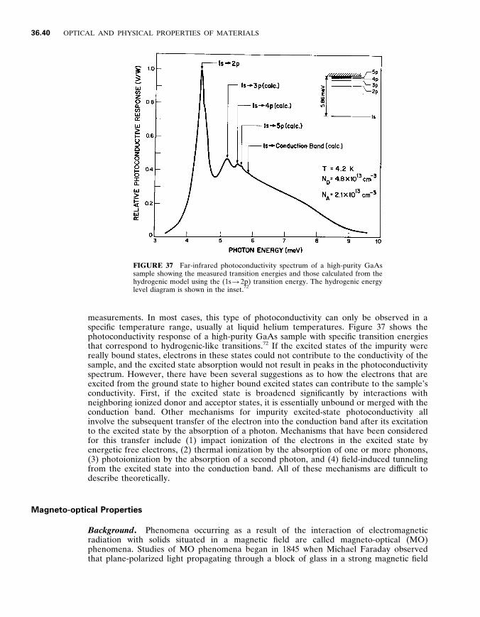
36 .40 OPTICAL AND PHYSICAL PROPERTIES OF MATERIALS
FIGURE 37 Far-infrared photoconductivity spectrum of a high-purity GaAs sample showing the measured transition energies and those calculated from the hydrogenic model using the (1s 5 2p) transition energy . The hydrogenic energy level diagram is shown in the inset . 7 2
measurements . In most cases , this type of photoconductivity can only be observed in a specific temperature range , usually at liquid helium temperatures . Figure 37 shows the photoconductivity response of a high-purity GaAs sample with specific transition energies that correspond to hydrogenic-like transitions . 7 2 If the excited states of the impurity were really bound states , electrons in these states could not contribute to the conductivity of the sample , and the excited state absorption would not result in peaks in the photoconductivity spectrum . However , there have been several suggestions as to how the electrons that are excited from the ground state to higher bound excited states can contribute to the sample’s conductivity . First , if the excited state is broadened significantly by interactions with neighboring ionized donor and acceptor states , it is essentially unbound or merged with the conduction band . Other mechanisms for impurity excited-state photoconductivity all involve the subsequent transfer of the electron into the conduction band after its excitation to the excited state by the absorption of a photon . Mechanisms that have been considered for this transfer include (1) impact ionization of the electrons in the excited state by energetic free electrons , (2) thermal ionization by the absorption of one or more phonons , (3) photoionization by the absorption of a second photon , and (4) field-induced tunneling from the excited state into the conduction band . All of these mechanisms are dif ficult to describe theoretically .
Magneto-optical Properties
Background . Phenomena occurring as a result of the interaction of electromagnetic radiation with solids situated in a magnetic field are called magneto-optical (MO) phenomena . Studies of MO phenomena began in 1845 when Michael Faraday observed that plane-polarized light propagating through a block of glass in a strong magnetic field

OPTICAL PROPERTIES OF SEMICONDUCTORS 36 .41
has its plane of vibration of light rotated . By the 1920s , most MO ef fects were fairly well understood in terms of the classical dynamics of an electron in a magnetic field . However , when semiconductors were first investigated in the early 1950s , a quantum mechanical interpretation of the MO data in terms of the energy-band structure was found to be necessary . The two major limitations of the classical theory are that no ef fects depending on the density of states are predicted and no ef fects of electron spin are included .
Table 8 presents an overview of the typical types of magneto-optical phenomena observed in semiconductors and the information that can be determined from the experimental measurements . Four classes of MO phenomena can be distinguished : those arising from (1) interband ef fects , (2) excitonic ef fects , (3) intraband or free-carrier ef fects , and (4) impurity magnetoabsorption ef fects . Further clarification can then be made by determining whether the ef fect is absorptive or dispersive , resonant or nonresonant , and upon the relative orientation of the magnetic field to the direction of propagation of the electromagnetic radiation and its polarization components . Resonant experiments usually provide more detailed information about the band structure of a semiconductor and often are easier to interpret . There is thus a wide variety of ef fects as shown which can give dif ferent types of information about the crystal’s energy-band structure , excitonic properties , and impurity levels . Before summarizing and discussing each of these magneto-optical ef fects , it is necessary to briefly describe the ef fects of a magnetic field on the enegy-band structure of a semiconductor .
Ef fect of a Magnetic Field on the Energy Bands . Magneto-optical experiments must be analyzed with specific energy-band models in order to extract the related band parameters and to emphasize the underlying physical concepts with a minimum of mathematical complexity . Most often , one deals with only the highest valence bands and the lowest conduction bands near the forbidden energy-gap region . If simple parabolic bands are assumed , a fairly complete analysis of the MO experiments is usually possible , including both the resonant frequencies and their line shapes . On the other hand , if more complicated energy bands (e . g ., degenerate , nonparabolic) are needed to describe the solid , the detailed analysis of a particular experiment can be complicated .
The ef fect of a magnetic field on a free electron on mass m * was determined in 1930 by Landau , who solved the Schroedinger equation . The free electrons experience a transverse Lorentz force which causes them to travel in orbits perpendicular to the magnetic field . The resulting energy eigenvalues corresponding to the transverse components of the wave vector are quantized in terms of harmonic oscillator states of frequency v c , while a plane-wave description characterizes the motion along the magnetic field . The allowed energy levels , referred to as Landau levels , are given by
E Ú
n 5 ( n 1 1 – 2 ) " v c 1 " 2 k 2
z
2 m * Ú
1 2
g * m B B (52)
where n is the Landau level number (0 , 1 , 2 , . . . ) , v c (the cyclotron frequency) is equal to eB / m * c , and m * c is the cyclotron ef fective mass . The middle term represents the energy of an electron moving along the direction of the B field in the z direction ; it is not quantized . The first term represents the quantized energy of motion in a plane perpendicular to the field . The last term represents the ef fect of the electron’s spin ; g * is the ef fective spectroscopic g -factor or spin-splitting factor and
m B 5 e " / 2 m 0 5 5 . 77 3 10 2 2 meV / T (53)
is the Bohr magneton . The g -factor in a semiconductor has values quite dif ferent from the usual value of two found for atomic systems (e . g ., for narrow-energy gaps and a strong spin-orbit interaction , g * can be large and negative) .

TABLE 8 Magneto-optical Phenomena and Typical Information Obtainable
Magneto-optical ef fect Some information or properties obtainable
Interband ef fects In transmission Band-to-band magnetoabsorption ....................................... Energy gaps , ef fective masses , g-factors , higher band
parameters Faraday rotation (resonant and nonresonant) ..................... Energy gaps , ef fective masses Faraday ellipticity (nonresonant) ......................................... Relaxation times Voigt ef fect (resonant and nonresonant) ............................. Ef fective masses Cross-field magnetoabsorption
In reflection Magnetoreflection ................................................................ Studies of very deep levels or where absorption is
high , similar information as in transmission magnetoabsorption
Kerr rotation Kerr ellipticity
Magneto-excitonic ef fects Diamagnetic and Zeeman shifts and splittings ;
energy gap ; ef fective reduced-mass tensor ; ef fective Rydberg ; anisotropy parameter ; dielectric tensor components ; ef fective g-factors ; ef fective masses ; quality of materials , structures , alloys and interfaces
Intraband or free-carrier ef fects
In transmission Cyclotron resonance (resonant) ........................................... Ef fective masses , relaxation times , nonparabolicity Combined resonance ........................................................... Same information as cyclotron resonance plus g-
factors Spin resonance ..................................................................... g-factors Phonon-assisted cyclotron resonance harmonics ................. Same information as cyclotron resonance plus
phonon information Faraday rotation (resonant and nonresonant) ..................... Carrier concentration , ef fective masses ; use for
impure materials , flexible , can be used at high temperature
Faraday ellipticity (nonresonant) Voigt ef fect (nonresonant) Interference fringe shift (nonresonant) Oscillatory variation of the Shubnikov-de Haas type .......... Carrier concentration
In reflection Magnetoplasma reflection .................................................... Ef fective masses , carrier concentration Magnetoplasma rotation (Kerr ef fect) Magnetoplasma ellipticity
Impurity magneto-absorption Zeeman and diamagnetic ef fect type behavior of impurities Hydrogenic impurity information , binding energy ,
ef fective masses , ef fective Rydberg , central cell corrections , static dielectric constant ; both impurity and Landau level information ; impurity information as above plus Landau-level information related to ef fective masses and g- factors
Photoionization behavior (transitions from ground state of impurity to Landau levels) ...............................................

OPTICAL PROPERTIES OF SEMICONDUCTORS 36 .43
FIGURE 38 Landau levels for simple bands . FIGURE 39 ( a ) Zincblende semiconductor energy bands ( H 5 0) ; and ( b ) in an applied magnetic field H . 7 3
Figure 38 shows schematically the ef fect of a magnetic field on a simple parabolic direct gap extrema at k 5 0 . The quasi-continuous parabolic behavior of the nondegenerate conduction and valence bands at B 5 0 (shown in a ) is modified by the application of a magnetic field into Landau levels as shown in b . Each Landau level is designated by an integer n 5 0 , 1 , 2 , 3 , . . . Finally , in Fig . 39 , the Landau ef fects are shown schematically for zincblende energy bands when both spin and valence-band degeneracy are taken into account for both B 5 0 ( a ) and B ? 0 ( b ) . 7 3 With spin included , the valence band splits into the G 8 and G 7 bands with spin-orbit splitting energy D . The quantization of the bands into Landau levels is illustrated in the right-hand side of the figure . The Pidgeon and Brown 7 4
model has been successfully used to describe the magnetic field situation in many semiconductors , since it includes both the quantum ef fects resulting from the partial degeneracy of the p-like bands and the nonparabolic nature of the energy bands . The a -set levels are spin-up states , and the b -set , the spin-down states . These large changes in the E versus k relations of the bands when a magnetic field is applied also means large changes in the density of states which become periodic with a series of peaks at energies corresponding to the bottom of each Landau level . This oscillatory variation in the density of states is important for understanding the various oscillatory phenomena in a magnetic field .
Interband Magneto - optical Ef fects . Interband transitions in a magnetic field connect Landau-level states in the valence band to corresponding states in the conduction band . Thus , they yield direct information concerning energy gaps , ef fective masses , ef fective g-factors , and higher band parameters . The strongest allowed transitions are those that are proportional to the interband matrix element p 5 2 ( i " / m o ) k s u p j u x j l , where j 5 x , y , z .
This matrix element directly connects the p-like valence band ( x , y , z ) which is triply degenerate with the s-like conduction band through the momentum operator p j . The transition energies can be calculated directly from a knowledge of the selection rules and use of an energy-band model . The selection rules are given by 7 5
s L : a ( n ) 5 a ( n 2 1) , b ( n ) 5 b ( n 2 1)
s R : a ( n ) 5 a ( n 1 1) , b ( n ) 5 b ( n 1 1)
π : a ( n ) 5 b ( n 1 1) , b ( n ) 5 a ( n 2 1)
where s L , s R , and π are left circular , right circular , and linear ( e i B ) polarizations . As discussed earlier , a and b denote the spin-up and spin-down states , and n the Landau-level

36 .44 OPTICAL AND PHYSICAL PROPERTIES OF MATERIALS
number . Often , sharp optical transitions between the Landau levels are observed , providing highly accurate information about the fundamental band parameters such as the energy gap E g , ef fective masses of the electrons and holes , higher band parameters , etc .
InSb is a material in which interband ef fects have been studied very extensively ; thus , it is a good representative example . Even though it is a narrow-gap semiconductor and thus has a small exciton binding energy , Weiler 7 6 has shown that excitonic corrections must be made to properly interpret the magnetic-field-dependent data . This shall be discussed in more detail in the next section . The band models discussed earlier predict that there is an increase in the energy of the absorption edge with magnetic field because of the zero point energy 1 / 2 " v c of the lowest conduction band . At larger photon energies , transmission minima (absorption maxima) which are dependent upon magnetic field are observed . By plotting the photon energy positions of the transmission minima against magnetic field , converging , almost linear plots are obtained as shown in Fig . 40 . 7 4 Extrapolation of the lines to zero field gives an accurate value for the energy gap . Use of a band model and specific transition assignments further allow the determination of other important band parameters , such as ef fective masses and g-factors .
Magnetoreflection . Besides the changes in absorption brought about by the magnetic field , there are changes in the refractive index . Since the reflectivity depends upon both the real and imaginary parts of the index , clearly it is af fected by the field . Interband transitions are often observed in reflection because of the high absorption coef ficients . Figure 41 shows the magnetoreflection behavior of InSb for s R and s L polarizations . 7 3 In addition , modulation spectroscopy techniques , in which a parameter such as stress , electric field , wavelength , magnetic field , etc . is periodically varied and the signal synchronously
FIGURE 40 Energy values of transmission minima versus magnetic field for electron transitions be- tween Landau levels of valence and conduction bands in InSb . Plot of the photon energy of the principal transmission minima as a function of mag- netic field for E i H i [100] . The solid lines represent the best theoretical fit to the experimental data . The numeral next to each line identifies the quantum assignment . 7 4
FIGURE 41 Magnetoreflection curves for InSb , compared to the magnetoabsorption results of Ref . 74 for InSb [001] with E ' H . " v # 5 387 . 1 meV ; T 5 24 K . 7 3
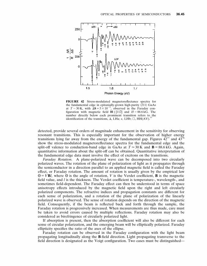
OPTICAL PROPERTIES OF SEMICONDUCTORS 36 .45
FIGURE 42 Stress-modulated magnetoreflectance spectra for the fundamental edge in epitaxially-grown high-purity k 211 l GaAs at T , 30 K , with D S 5 5 3 10 2 5 , observed in the Faraday con- figuration with magnetic field H i [112 # ] and H 5 88 . 6 kG . The number directly below each prominent transition refers to the identification of the transitions , D , LHa ; x , LHb ; h , HH(AV) . 7 7
detected , provide several orders of magnitude enhancement in the sensitivity for observing resonant transitions . This is especially important for the observation of higher energy transitions lying far away from the energy of the fundamental gap . Figures 42 7 7 and 43 7 8
show the stress-modulated magnetoreflectance spectra for the fundamental edge and the split-of f valence to conduction-band edge in GaAs at T < 30 K and B 5 88 . 6 kG . Again , quantitative information about the split-of f can be obtained . Quantitative interpretation of the fundamental edge data must involve the ef fect of excitons on the transitions .
Faraday Rotation . A plane-polarized wave can be decomposed into two circularly polarized waves . The rotation of the plane of polarization of light as it propagates through the semiconductor in a direction parallel to an applied magnetic field is called the Faraday ef fect , or Faraday rotation . The amount of rotation is usually given by the empirical law Θ 5 V B l , where Θ is the angle of rotation , V is the Verdet coef ficient , B is the magnetic field value , and l is the thickness . The Verdet coef ficient is temperature- , wavelength- , and sometimes field-dependent . The Faraday ef fect can then be understood in terms of space anisotropy ef fects introduced by the magnetic field upon the right and left circularly polarized components . The refractive indices and propagation constants are dif ferent for each sense of polarization , and a rotation of the plane of polarization of the linearly polarized wave is observed . The sense of rotation depends on the direction of the magnetic field . Consequently , if the beam is reflected back and forth through the sample , the Faraday rotation is progressively increased . When measurements are thus made , care must be taken to avoid errors caused by multiple reflections . Faraday rotation may also be considered as birefringence of circularly polarized light .
If absorption is present , then the absorption coef ficient will also be dif ferent for each sense of circular polarization , and the emerging beam will be elliptically polarized . Faraday ellipticity specifies the ratio of the axes of the ellipse .
Faraday rotation can be observed in the Faraday configuration with the light beam propagating longitudinally along the B -field direction . Light propagating transverse to the field direction is designated as the Voigt configuration . Two cases must be distinguished—

36 .46
OPTICAL AND PHYSICAL PROPERTIES OF MATERIALSFIGURE 43 Stress-modulated magnetoreflectance spectra for the split-of f valence-to-conduction band tran- sitions in GaAs at T < 30 K with D S 5 5 3 10 2 5 in the Faraday configuration for the same conditions as for Fig . 42 . The zero-field spectrum is displaced upward for clarity . For bottom curve , H 5 88 . 6 kG , RCP is solid line , and LCP is dashed line . 7 8
the incident beam may be polarized so that its E field is either parallel or perpendicular to B . The Voigt ef fect is birefringence induced by the magnetic field and arises from the dif ference between the parallel and perpendicular indices of refraction in the transverse configuration . It is usually observed by inclining the incident plane-polarized radiation with the electric vector at 45 8 to the direction of B . The components resolved parallel and perpendicular to B then have dif ferent phase velocities , and recombine at the end of the sample to give emerging radiation which is elliptically polarized . Measurements of this ellipticity then determine the Voigt ef fect .
The interband Faraday ef fect is a large ef fect and is therefore useful for characterizing semiconductors . For frequencies smaller than the frequency corresponding to the energy gap , the interband Faraday ef fect arises from the dispersion associated with the interband magnetoabsorption . In this region , it has been used to determine energy gaps and their pressure and temperature dependence . Since the beam propagates through the crystal in a transparent region of the spectrum , it may be attractive to use in certain applications . Figure 44 shows the Verdet coef ficient versus wavelength for GaAs at two temperatures , 298 and 77 K , and for B 5 20 kG . 7 9 At long wavelengths it has a positive rotation , while near the gap the Verdet coef ficient becomes negative . For frequencies equal to or larger than the frequency corresponding to the energy gap , the Faraday rotation is dominated by the nearest magneto-optical transition . Oscillatory behavior , like that seen in the magnetoabsorption , is also often observed .
Diluted magnetic semiconductors (DMS) are a class of materials that have been attracting considerable scientific attention . Any known semiconductor with a fraction of its constituent ions replaced by some species of magnetic ions (i . e ., ions bearing a net magnetic moment) can be defined as a member of this group . The majority of DMS studied so far have involved Mn 1 2 ions embedded in various II – VI hosts . One important aspects of DMS controlling their optical properties is the interaction between the localized

OPTICAL PROPERTIES OF SEMICONDUCTORS 36 .47
FIGURE 44 Interband Faraday rotation in GaAs . 7 9
magnetic moments of Mn 1 2 and the conduction- and / or valence-band electrons (referred to as the sp-d interaction) which results in features unique to DMS . The best known (and quite spectacular) of these are the huge Faraday rotations of the visible and near-infrared light in wide-gap DMS . The origin of the large rotations is the sp-d exchange interaction which makes the band structure much more sensitive to the strength of external magnetic fields than in ordinary semiconductors . Figure 45 shows the Faraday ef fect in Cd 1 2 x Mn x Se( x 5 0 . 25) at T 5 5 K . 8 0 Each successive peak represents an additional Faraday rotation of 180 8 . The absolute Faraday rotation as a function of frequency is determined by monitoring the transmission at several fixed photon energies as the magnetic field is swept .
Excitonic Magneto - optical Ef fects . As described earlier , a free exciton consists of an electron and hole bound together electrostatically . When the pair has an energy less than
FIGURE 45 Faraday ef fect in Cd 1 2 x Mn x Se ( x 5 0 . 25) , T 5 5 K . The dashed line represents the transmission of light as a function of its frequency for a 3-mm-thick sample located between two polaroids with their axes at 45 8 and at zero magnetic field . The light propagates along the optic axis , c . The oscillations occur when a 10-kG magnetic field is applied along c . 8 0
36 .48 OPTICAL AND PHYSICAL PROPERTIES OF MATERIALS
that of the energy gap , they orbit around each other . If the orbital radius is large compared with the lattice constant , they can be approximately treated as two point charges having ef fective masses and being bound together by a Coulomb potential that gives rise to a hydrogen-atom-like behavior . In the presence of a magnetic field , excitons give rise to Zeeman and diamagnetic ef fects analogous to those in atomic spectra . Fine structure can occur due to motions other than the simple orbiting of an electron and hole—the carriers can have intrinsic motion , motion around an atom , spin motion , and motion of the complete exciton through the lattice . Some of these motions may even be coupled together .
Bound excitons (or bound-exciton complexes) or impurity-exciton complexes are extrinsic properties of materials . Bound excitons are observed as sharp-line optical transitions in both photoluminescence and absorption . The bound exciton is formed by binding a free exciton to a chemical impurity atom (or ion) , a complex , or a host lattice defect . The binding energy of the exciton to the impurity or defect is generally smaller than the free-exciton binding energy . The resulting complex is molecularlike (hydrogen- molecule-like) , and bound excitons have many spectral properties analogous to those of simple diatomic molecules .
The application of a magnetic field to samples where excitonic features are observed in the absorption spectra results in line splittings , energy shifts , and changes in linewidths . These arise from diamagnetic and Zeeman ef fects just as in atomic or molecular spectroscopy . The treatment of the problem of an exciton in a magnetic field in zincblende-type structures is dif ficult due to the complexity of the degenerate valence band . Often a practical solution is adopted that corrects the interband model calculations for exciton binding energies that are dif ferent for each Landau level . Elliott and Loudon showed that the absorption spectrum has a peak corresponding to the lowest N 5 0 hydrogen-like bound state of the free exciton , which occurs below the free interband transition by the exciton binding energy E B . 8 1 Weiler suggests that for transitions to the conduction-band Landau level n , the exciton binding energy E B can be approximated by 7 3
E B ( n ) < 1 . 6 R [ g B / (2 n 1 1)] 1/3 (54)
where R is the ef fective Rydberg ,
R 5 R 0 m / m 0 e (0) (55)
R o 5 13 . 6 eV , e (0) is the static-dielectric constant , m is the reduced ef fective mass for the transition , and g B is the reduced magnetic field
g B 5 m o S / 2 m R (56)
and
S 5 " eB / m o (57)
Thus after calculating the interband transition energy for a particular conduction-band Landau level n , one subtracts the above binding energy to correct for exciton ef fects .
Nondegenerate semiconductors , in particular , materials belonging to the wurtzite crystal structure , have been extensively studied both with and without a magnetic field . Exciton states in CdS have been studied by high-resolution two-photon spectroscopy in a magnetic field using a fixed near-infrared beam and a tunable visible dye laser . 82 , 83 Figure 46 shows the photoconductive response versus total photon energy near the A-exciton region . 8 2 The two-photon transitions involve P states and both 2P and 3P states are clearly seen . As the field is increased , both Zeeman splittings and diamagnetic shifts occur . Figure

OPTICAL PROPERTIES OF SEMICONDUCTORS 36 .49
FIGURE 46 Photoconductivity vs . total photon energy " v v 1 " v i r near the A -exciton region in CdS platelets for various magnetic fields . The magnetic field was parallel to the hexagonal c axis in a Voigt configuration with E perpendicular to c for the two photons at a lattice temperature of T L 5 1 . 8 K . The instrumental resolution R 5 0 . 1 meV is narrower than the intrinsic linewidths . 8 2
FIGURE 47 Peak positions , in total photon energy " v v 1 " v i r for the 2 P and 3 P A excitons in CdS platelets as a function of applied B field . The solid points were determined experimentally and the solid curves are theoretically obtained from variational calculations of the diamagnetic shifts along with use of the experimental g factors . 8 2
47 shows both experimental and theoretical transition energies versus B field . 8 2 Excellent agreement is obtained by using variational calculations that have been successfully used to describe impurity atoms in a magnetic field .
Intraband or Free - carrier Ef fects Cyclotron Resonance . The simplest and most fundamental magneto-optical ef fect ,
cyclotron resonance absorption of free carriers , provides a direct determination of carrier ef fective masses . Classically , it is a simple phenomenon—charged particles move in circular orbits (in planes perpendicular to the direction of the magnetic field) whose radii increase as energy is absorbed from the applied electric fields at infrared or microwave frequencies . After a time τ , a collision takes place and the absorption process begins again . From the resonance relation v c 5 e B / m * , extensive and explicit information about the ef fective masses and the shape of energy surfaces near the band extrema can be obtained . Excellent reviews of cyclotron resonance have been previously published by McCombe and Wagner 84 , 85 and Otsuka . 8 6
A classical example of the explicit band structure information that can be obtained

36 .50 OPTICAL AND PHYSICAL PROPERTIES OF MATERIALS
FIGURE 48 Microwave absorption in intrinsic n -type Ge at 4 . 2 K for four dif ferent directions of B in the (1 # 10) plane as a function of the magnetic field . P 35 8 represents the absorption with B at 35 8 to the [001] axis . 8 7
from cyclotron resonance experiments is given for Ge . Figure 48 shows the microwave absorption for n -type germanium at 4 . 2 K for four dif ferent B field directions , each peak corresponding to a specific electron ef fective mass . 8 7 Figure 49 shows the orientation dependence of the ef fective masses obtained from the cyclotron resonance experiments which demonstrates that there is a set of crystallographically equivalent ellipsoids oriented along all k 111 l directions in the Brillouin zone . 8 8 Figure 50 shows the band structure of Ge that these measurements helped to establish 8 9 : a illustrates the conduction band minima along the k 111 l direction at the zone edge and b , the eight half-prolate ellipsoids of revolution or four full ellipsoids . The longitudinal and transverse masses are m * l 5 1 . 6 m o
FIGURE 49 Ef fective mass of electrons in Ge at 4 K for magnetic field directions in a (110) plane . 8 8

OPTICAL PROPERTIES OF SEMICONDUCTORS 36 .51
FIGURE 50 ( a ) Band structure of Ge plotted along the [100] and [111] directions ; ( b ) ellipsoidal energy surface corresponding to primary valleys along the k 111 l directions . 8 9
and m * t 5 0 . 082 m o , respectively . Both holes and electrons could be studied by using light to excite extra carriers . This illustrates the use of cyclotron resonance methods to obtain band structure information . Since that time , numerous experiments have been carried out to measure ef fective mass values for carriers in various materials .
The beginning of modern magneto-optics in which ‘‘optical’’ as opposed to ‘‘micro- wave’’ techniques were used , began in 1956 with the use of infrared frequencies at high magnetic fields . Far-infrared lasers are extremely important for modern-day measurements of cyclotron resonance as seen in Fig . 51 for n -type InSb . 9 0 At low temperatures , only the lowest CR transition C 1 (0 1 to 1 1 ) is seen . Raising the temperature populates the higher-lying Landau levels , and other CR transitions are seen at dif ferent fields because of the nonparabolicity of the conduction band which gives rise to an energy-dependent ef fective mass . At 13 K , a second transition C 2 (0 2 to 1 2 ) is seen and at 92 K , C 3 (1 1 to 2 1 ) . The low field feature denoted by I is called impurity cyclotron resonance because , although it is a neutral donor excitation , its appearance resembles that of the regular CR magnetoabsorption . It results from neutral donors exhibiting a Zeeman transition (1s 5 2p 1 ) , the transition energy of which is much larger than the ionization energy . The I signal gradually disappears as the temperature increases because the donors become ionized .
Cyclotron resonance also serves as a valuable tool for materials characterization through making use of the cyclotron resonance linewidth and intensity . Resonance linewidths can dif fer considerably from sample to sample . This dif ference in linewidth is attributed to dif ferences in impurity content , with the higher-purity samples having the narrowest linewidths and largest intensities . Figure 52 shows the electron CR signals for both n -type and p -type GaAs crystals with low compensation . 8 6 The observed large dif ference in linewidths is primarily considered to reflect the dif ference in the electron- donor and electron-acceptor scattering rates .
An electron placed in the conduction band of a polar insulator or semiconductor surrounds itself with an induced lattice-polarization charge . The particle called a polaron consists of the electron with its surrounding lattice-polarization charge . The term magnetopolaron is also often referred to as a polaron in a magnetic field . Landau-level energies of these magnetopolarons are shifted relative to those predicted for band electrons . These energy shifts give rise to polaron ef fects that are most clearly evident in optical experiments such as cyclotron resonance . The recent review by Larsen provides an annotated guide to the literature on polaron ef fects in cyclotron resonance . 9 1
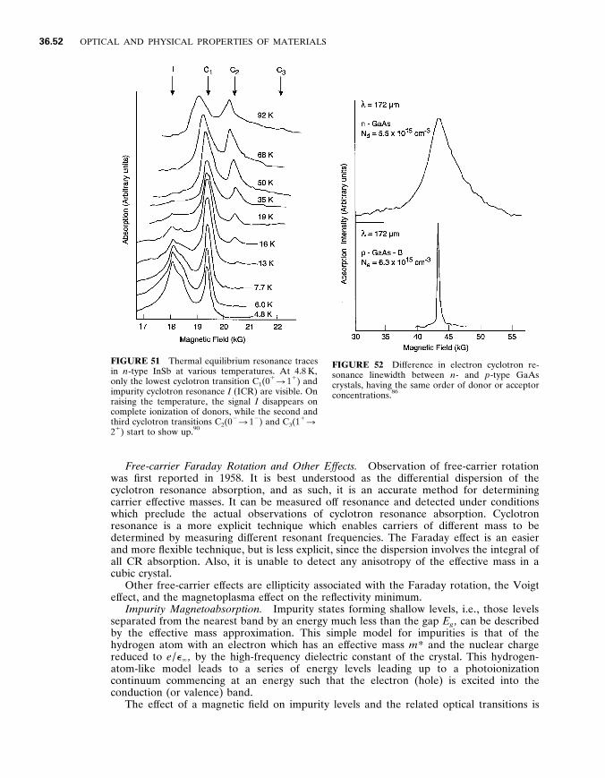
36 .52 OPTICAL AND PHYSICAL PROPERTIES OF MATERIALS
FIGURE 51 Thermal equilibrium resonance traces in n -type InSb at various temperatures . At 4 . 8 K , only the lowest cyclotron transition C 1 (0 1
5 1 1 ) and impurity cyclotron resonance I (ICR) are visible . On raising the temperature , the signal I disappears on complete ionization of donors , while the second and third cyclotron transitions C 2 (0 2
5 1 2 ) and C 3 (1 1 5
2 1 ) start to show up . 9 0
FIGURE 52 Dif ference in electron cyclotron re- sonance linewidth between n - and p -type GaAs crystals , having the same order of donor or acceptor concentrations . 8 6
Free - carrier Faraday Rotation and Other Ef fects . Observation of free-carrier rotation was first reported in 1958 . It is best understood as the dif ferential dispersion of the cyclotron resonance absorption , and as such , it is an accurate method for determining carrier ef fective masses . It can be measured of f resonance and detected under conditions which preclude the actual observations of cyclotron resonance absorption . Cyclotron resonance is a more explicit technique which enables carriers of dif ferent mass to be determined by measuring dif ferent resonant frequencies . The Faraday ef fect is an easier and more flexible technique , but is less explicit , since the dispersion involves the integral of all CR absorption . Also , it is unable to detect any anisotropy of the ef fective mass in a cubic crystal .
Other free-carrier ef fects are ellipticity associated with the Faraday rotation , the Voigt ef fect , and the magnetoplasma ef fect on the reflectivity minimum .
Impurity Magnetoabsorption . Impurity states forming shallow levels , i . e ., those levels separated from the nearest band by an energy much less than the gap E g , can be described by the ef fective mass approximation . This simple model for impurities is that of the hydrogen atom with an electron which has an ef fective mass m * and the nuclear charge reduced to e / e , by the high-frequency dielectric constant of the crystal . This hydrogen- atom-like model leads to a series of energy levels leading up to a photoionization continuum commencing at an energy such that the electron (hole) is excited into the conduction (or valence) band .
The ef fect of a magnetic field on impurity levels and the related optical transitions is

OPTICAL PROPERTIES OF SEMICONDUCTORS 36 .53
one of the most important tools for the study of the electronic states . The reason for this is that a magnetic field removes all degeneracies including the Kramers’ degeneracy due to time reversal . It can produce new quantization rules , and it is a strong perturbation which is not screened like the Coulomb interactions .
For donor states with an isotropic conduction-band minimum , as in GaAs or InSb , the Hamiltonian acquires terms which are linear (Zeeman term) and quadratic (diamagnetic) in magnetic field . In this case , perturbation theory is appropriate to use until one considers transitions to very high quantum numbers or very high fields . Often complicated variational procedures must be used for accurate solutions . In the high field limit where " v c / R 1 or for high energies , the impurity level quantum numbers do not provide a proper classification , and instead , the states should be related to the continuum Landau levels . The ef fect of a magnetic field on acceptor impurity states is more complicated because of band degeneracy and of spin-orbit coupling . Also for acceptors , one can be in the high field limit at relatively small values of the field for shallow levels and for excited states .
High-resolution photoconductivity measurements in high-purity GaAs indicate that the behavior of shallow donors in GaAs deviates from that predicted by the simple hydrogenic model . Figure 53 shows that under high resolution , the single (1s 5 2p) transition observed at lower resolution actually consists of several dif ferent unresolved transitions . 9 2 The photoconductive response is shown for two dif ferent high-purity GaAs samples . The magnetic field range shown covers about 1 kG at around 15 kG . The dif ferent transitions labeled A , B , C , and D each correspond to a dif ferent donor species , and variation of the amplitude of these transitions in dif ferent samples results from the dif ferent relative concentrations of the particular donor species . Thus , the use of magnetic fields in studying the absorption properties of shallow impurities has opened up a new analytical method of impurity characterization . Because of the central-cell corrections (chemical shifts) , dif ferent impurities of the same type (donor or acceptors) can be distinguished and identified by back-doping experiments .
FIGURE 53 The photoconductivity due to the (1s 5 2p , m 5 1 1) transition as a function of mag- netic field for two dif ferent samples when excited by 190 m m laser radiation . For sample 1 , N D 5 2 . 0 3 10 1 4 cm 2 3 , N A 5 4 . 0 3 10 1 3 cm 2 3 , m 77K 5 153 , 000 cm 2 / V-s . For sample 2 , N D 5 4 . 3 3 10 1 3 cm 2 3 , N A 5 2 . 5 3 10 2 1 3 cm 2 3 , and m 77K 5 180 , 000 cm 2 / V-s . 9 2
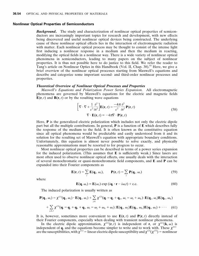
36 .54 OPTICAL AND PHYSICAL PROPERTIES OF MATERIALS
Nonlinear Optical Properties of Semiconductors
Background . The study and characterization of nonlinear optical properties of semicon- ductors are increasingly important topics for research and development , with new ef fects being discovered and useful nonlinear optical devices being constructed . The underlying cause of these nonlinear optical ef fects lies in the interaction of electromagnetic radiation with matter . Each nonlinear optical process may be thought to consist of the intense light first inducing a nonlinear response in a medium and then the medium in reacting , modifying the optical fields in a nonlinear way . There is a wide variety of nonlinear optical phenomena in semiconductors , leading to many papers on the subject of nonlinear properties . It is thus not possible here to do justice to this field . We refer the reader to Tang’s article on Nonlinear Optics in this Handbook (Vol . II , Chap . 38) . 9 3 Here , we give a brief overview of the nonlinear optical processes starting from Maxwell’s equations and describe and categorize some important second- and third-order nonlinear processes and properties .
Theoretical O y er y iew of Nonlinear Optical Processes and Properties Maxwell ’ s Equations and Polarization Power Series Expansion . All electromagnetic
phenomena are governed by Maxwell’s equations for the electric and magnetic fields E ( r , t ) and B ( r , t ) or by the resulting wave equations
(58) F = ? = 1
1 c 2
2
t 2 G E ( r , t ) 5 2 4 π
c 2
2
t 2 P ( r , t )
= ? E ( r , t ) 5 2 4 π = ? P ( r , t )
Here , P is the generalized electric polarization which includes not only the electric dipole part but all the multiple contributions . In general , P is a function of E which describes fully the response of the medium to the field . It is often known as the constitutive equation since all optical phenomena would be predictable and easily understood from it and its solution for the resulting set of Maxwell’s equation with appropriate boundary conditions . Unfortunately , this equation is almost never possible to solve exactly , and physically reasonable approximations must be resorted to for progress to occur .
Most nonlinear optical properties can be described in terms of a power series expansion for the induced polarization . (This assumes that E is suf ficiently weak . ) Since lasers are most often used to observe nonlinear optical ef fects , one usually deals with the interaction of several monochromatic or quasi-monochromatic field components , and E and P can be expanded into their Fourier components as
E ( r , t ) 5 O i
E ( q i , v i ) , P ( r , t ) 5 O i
P ( q i , v i ) (59)
where E ( q i v i ) 5 E ( v i ) exp ( i q i ? r 2 i v i t ) 1 c . c . (60)
The induced polarization is usually written as
P ( q i , v i ) 5 χ (1) ( q i , v i ) ? E ( q i , v i ) 1 O j ,k
χ (2) ( q i 5 q j 1 q k , v i 5 v j 1 v k ) : E ( q j , v j ) E ( q k , v k )
(61) 1 O j ,k ,l
χ (3) ( q i 5 q j 1 q k 1 q l , v i 5 v j 1 v k 1 v l ) : E ( q j , v j ) E ( q k , v k ) E ( q l , v l ) 1 ? ? ?
It is , however , sometimes more convenient to use E ( r , t ) and P ( r , t ) directly instead of their Fourier components , especially when dealing with transient nonlinear phenomena .
In the electric dipole approximation , χ ( n ) ( r , t ) is independent of r , or χ ( n ) ( k , v ) is independent of q , and the equations become simpler to write and to work with . These χ ( n ) are the susceptibilities , with χ (1) 5 linear electric dipole susceptibility and χ (2) ( χ (3) ) 5 nonlinear

OPTICAL PROPERTIES OF SEMICONDUCTORS 36 .55
second-order (third-order) susceptibility tensor . Both absorptive and refractive ef fects can be described in terms of these complex electric susceptibilities , which have real and imaginary parts for each tensor element . These linear and nonlinear susceptibilities characterize the optical properties of the medium and are related to the microscopic structure of the medium . Knowledge of χ ( n ) allows , at least in principle , to predict the n th-order nonlinear optical ef fects from Maxwell’s equations . Consequently , much ef fort (both experimentally and theoretically) has gone into determining the χ ( n ) .
The definitions of the nonlinear susceptibilities in the literature vary and have led to some confusion . Shen reviews these definitions and the reasons for the confusion . 9 4 In addition to some intrinsic symmetries , the susceptibilities must obey crystallographic symmetry requirements . The spatial symmetry of the nonlinear medium imposes restric- tions upon the form of the various χ ( n ) tensors . Butcher has determined the structure of the second- and third-order tensors for all crystals . 9 5 One important consequence is that for media with inversion symmetry , χ (2) ; 0 , and thus χ (3) represents the lowest-order nonlinearity in the electric-dipole approximation . Of the 12 nonzero elements , only 3 are independent . These susceptibility tensors must transform into themselves under the point group symmetry operations of the medium .
It is often convenient to discuss the various optical processes which might occur in terms of whether they are active or passive . Passive processes involve energy or frequency conservation , and the material medium acts basically as a catalyst . The susceptibilities are predominantly real for passive processes . Of course , as resonances are approached , susceptibilities become complex and may even become totally imaginary . These passive nonlinear optical phenomena are listed in Table 9 . 9 6 Active nonlinear optical phenomena
TABLE 9 Passive Nonlinear Optical Phenomena 9 6
Frequencies of incident
fields
Frequencies of fields generated by the
polarization of the medium Susceptibility Process (acronym)
v 1 No polarization 0( e 5 1) Vacuum propagation (VP) v 1 v 1 χ (1) ( v 1 ; v 1 ) Linear dispersion (LD)
v 1 , v 2 v 3 [ v 3 5 v 1 1 v 2 ] χ (2) ( v 3 ; v 1 , v 2 ) Sum mixing (SM) v 1 v 3 [ v 3 5 2 v 1 ] χ (2) ( v 3 ; v 1 , v 1 ) Second-harmonic
generation (SHG) v 1 , 0 v 1 χ (2) ( v 1 ; v 1 , 0) Electro-optic linear Kerr
ef fect (EOLKE) v 1 v 2 , v 3 [ v 1 5 v 2 1 v 3 ] χ (2) ( v 2 ; 2 v 3 , v 1 ) Dif ference-frequency
mixing (DFM) v 1 v 2 [ v 1 5 2 v 2 ] χ (2) ( v 2 ; 2 v 2 , v 1 ) Degenerate dif ference-
frequency (DDF) v 1 0 χ (2) (0 ; 2 v 1 , v 1 ) Inverse electro-optic ef fect
(IEOE) v 1 , v 2 , v 3 v 4 [ v 4 5 v 1 1 v 2 1 v 3 ] χ (3) ( v 4 ; v 1 , v 1 , v 1 ) Third-harmonic generation
(THG) v 1 , v 2
v 1
v 3 , v 4 [ v 1 1 v 2 5 v 3 1 v 4 ]
v 2 , v 3 , v 4 [ v 1 5 v 2 1 v 3 1 v 4 ]
χ (3) ( v 3 ; 2 v 4 , v 1 , v 2 ) χ (3) ( v 4 ; 2 v 3 , v 1 , v 2 )
χ (3) ( v 2 ; 2 v 3 , 2 v 4 , v 1 )
Four-wave dif ference- frequency mixing processes (FWDFMP)
v 1 v 1 χ (3) ( v 1 ; v 1 , 2 v 1 , v 1 ) Intensity-dependent refractive index (IDRI)
v 1 , 0 v 1 χ (3) ( v 1 ; 0 , 0 , v 1 ) Quadratic Kerr ef fect (QKE)
v 5 0 indicates the presence of a uniform electric field .
36 .56 OPTICAL AND PHYSICAL PROPERTIES OF MATERIALS
TABLE 10 Active Nonlinear Optical Phenomena 9 6
Susceptibility Process
χ (1) ( v 1 ; v 1 ) χ (3) ( v 2 ; v 1 , 2 v 1 , v 2 ) χ (3) ( v 1 ; v 1 , 2 v 1 , v 1 )
χ (5) ( v 2 ; v 1 , v 1 , 2 v 1 , 2 v 1 , v 2 )
Linear absorption ( v 1 < v 1 0 ) Raman scattering ( v 2 < v 1 Ò v 1 0 ) Two-photon absorption (2 v 1 < v 1 0 ) or
Saturable absorption ( v 1 < v 1 0 ) Hyper-Raman scattering ( v 2 < 2 v 1 Ò v 1 0 )
are listed in Table 10 . 9 6 In general , energy is exchanged between the radiation and the material only for the active processes . We also note that second-order ef fects are always passive .
Second - order Nonlinear Optical Properties . Most existing nonlinear optical devices are based upon second-order nonlinear optical ef fects that are quite well understood . Here , we assume the presence of only three quasi-monochromatic fields
E 5 E ( v 1 ) 1 E ( v 2 ) 1 E ( v 3 ) (62) and
v 1 5 u v 2 Ò v 3 u (63)
Thus , Eq . (58) can be decomposed into three sets of equations for each E ( v i ) . They are then nonlinearity coupled with one another through the polarizations
P ( v 1 ) 5 χ (1) ( v 1 ) ? E ( v 1 ) 1 χ (2) ( v 1 5 u v 2 Ú v 3 u ) : E ( v 2 ) E ( v 3 ) (64)
The second-order nonlinear processes are then described by the solutions of the coupled-wave equations with the proper boundary conditions . χ (2) 5 0 for materials with a center of inversion . The coef ficient χ (2) is a third-rank tensor . Some second-order processes include sum- and dif ference-frequency mixing , the electro-optic linear Kerr ef fect , the inverse electro-optic ef fect , parametric amplification and oscillation , and second-harmonic generation . The past emphasis has been on finding new nonlinear crystals with a large χ (2) . Semiconductor crystals have received much attention : III-V compounds like GaAs and InSb , II-VI compounds like ZnS and CdSe , I-III-VI compounds like AgGaS 2 and CuInS 2 , and II-IV-V compounds like CdSiAs 2 and ZnGeP 2 .
In most applications of second-order nonlinear optical ef fects , it is important to achieve phase-matching conditions
D q 5 q 1 2 q 2 2 q 3 5 0 (65)
where q i is the wave vector of E ( v i ) . This ensures an ef ficient energy conversion between the pump field(s) and the signal field .
Third - order Nonlinear Optical Properties . In materials with inversion symmetry , third-order processes are the dominant nonlinearity . These processes are described by a fourth-rank nonlinear susceptibility tensor χ (3) whose contribution to the polarization is given according to Eq . (61) by
P ( v i ) 5 O j ,k ,l
v (3) ( v i 5 v j 1 v k 1 v l ) : E ( v j ) E ( v k ) E ( v l ) (66)
In general , this nonlinearity will provide a coupling between four electromagnetic waves . Depending on whether the susceptibility tensor elements are real or imaginary and on whether some of the frequencies are identical or dif ferent , a large variety of physical phenomena can be understood and accounted for : third-harmonic generation , two-photon absorption , saturable absorption , intensity-dependent index of refraction , stimulated

OPTICAL PROPERTIES OF SEMICONDUCTORS 36 .57
Raman ef fect , anti-Stokes generation , stimulated Raleigh scattering , modulation of the index of refraction , and self-focusing of light . We concentrate on discussing only a few of the most pertinent cases of interest .
Third - harmonic Generation . Here , the output frequency v 4 5 v 1 1 v 2 1 v 3 5 3 v 1 since v 1 5 v 2 5 v 3 . The polarization at the frequency v 4 will generate radiation at the third-harmonic frequency . The quantum process responsible for the harmonic generation may be described as a scattering process in which three quanta at the fundamental frequency are annihilated and one quantum at the third-harmonic frequency is created . The system remains in the ground state , although three virtually excited states are involved in the scattering process . Since the phases are important , the process is actually an interference between many four-photon scattering processes .
Two-photon Absorption . Here , for example , v 1 5 2 v 2 5 v 3 5 v 4 and D k 5 0 , and the nonlinear polarization has components described by
P ( v 4 ) 5 χ (3) ( v 4 5 1 v 1 2 v 2 1 v 3 ) : E ( v 1 ) E *( v 2 ) E ( v 3 ) (67)
The nonlinear susceptibility χ (3) is purely imaginary , but positive . One can define an absorption coef ficient proportional to the intensity itself . In the important case of resonance , the sum of two frequencies of the exciting field is approximately equal to a transition frequency of the medium , v a b 5 2 v 1 , where " v a b is the energy dif ference between two levels u a l and u b l with the same parity .
The TPA coef ficient can be expressed in terms of a third-order nonlinear susceptibility tensor by solving the wave equation using the slowly varying amplitude approximation . The explicit expression for b is related to the imaginary part of the third-order electric dipole susceptibility tensor which depends upon the crystal class and laser electric field direction , for example , in crystals with 4 # 3 m symmetry (e . g ., Hg 1 2 x Cd x Te , GaAs , InSb , etc . ) and the electric field along the [001] direction , 9 7
b 5 32 π 2 v
n 2 c 2 [3 Im χ (3) 1111 ( 2 v , v , v , 2 v )] (68)
where the convention used is that of Maker and Terhune (1965) . 9 8
Since χ (3) is a second-rank tensor , there are , in general , nine terms contributing to b with magnitudes which vary with orientation . However , in most systems the symmetry is such that there are relations between certain of the terms . For example , in crystals with 4 # 3 m symmetry , there are three possible values of χ for each b , and for crystals with m3m symmetry , there are four possible values . These can , in general , be measured by using both linearly and circularly polarized light . It is not always possible to sort out all the dif ferent TPA spectra simply by changing the sample orientation or the light polarization because of the competing process of absorption by second-harmonic-produced light .
Simulated Raman Scattering or Coherent Raman Spectroscopy . Levenson (1977) has written an excellent review of this area in Physics Today . 9 9
Raman scattering provides a tool for the spectroscopic investigation of energy levels not accessible by the usual absorption or emission techniques . However , until the development of lasers , Raman scattering was a laborious and exotic technique . Now with coherent Raman techniques , the Raman modes are made to emit a beam of coherent radiation containing the details of the spectrum . The power in the beam can be many orders of magnitude larger than that in the spontaneously scattered radiation , and spatial filtering can be used to separate the output beam from the unwanted radiation .
Here , we can write
P ( v 4 ) 5 χ (3) ( v 4 5 Ú ( v 1 2 v 2 ) 1 v 3 ) E ( v 1 ) E *( v 2 ) E ( v 3 ) (69)
The electric field with frequency components at v 1 and v 2 produces a force with Fourier components at Ú ( v 1 2 v 2 ) which can then drive a Raman mode resonantly when

36 .58 OPTICAL AND PHYSICAL PROPERTIES OF MATERIALS
u v 1 2 v 2 u < v R . The polarization in Eq . (66) acts as a source term in Maxwell’s equation to produce the output beam at v 4 . Besides this resonant contribution to χ (3) , there also can be nonresonant contributions to χ (3) . The resonant Raman term interferes constructively and destructively with the nonresonant background which can become a nuisance .
There are a variety of coherent Raman spectroscopic techniques which can be used in observing Raman spectra by means of nonlinear optical mixing . Each technique has its own set of advantages and disadvantages , and it is important to match the technique properly to the investigation .
CARS ( Coherent Anti - Stokes Raman Scattering , or Spectroscopy ) . This is the most widely used technique of coherent Raman spectroscopy . In this case , two incident laser frequencies v 1 and v 2 are employed with v 3 5 v 1 , giving an output frequency v 4 5 1 ( v 1 2 v 2 ) 1 v 3 5 2 v 1 2 v 2 . With v 1 corresponding to the laser frequency in a spontaneous-scattering experiment and v 2 to the Stokes-scattered photon , the output occurs at the corresponding anti-Stokes frequency ( v 1 2 v 2 . 0) . An analogous technique with v 1 2 v 2 , 0 is called Coherent Stokes Raman Spectroscopy , or CSRS .
Two lasers are focused into a sample with an angle between the beams which best fulfills the wave-vector-matching conditions for the overall three-wave mixing process D q 5 0 . In solids , this depends upon v 1 2 v 2 and the dispersion of the index of refraction . The beam emerging from the sample at v 4 is selected by means of filters or a monochromator , and its intensity is then detected . The dif ference frequency v 1 2 v 2 is varied by tuning one or both lasers which gives the Raman spectrum of the sample in the output plotted as a function of v 1 2 v 2 . This is a potentially powerful technique with resolution limited by the laser linewidth . However , in solids , to be able to see weak spectroscopically interesting modes by coherent techniques , it becomes necessary to suppress the nonresonant background . Without this suppression , coherent Raman tech- niques are actually less ef fective than spontaneous scattering in detecting Raman spectra of condensed phases .
RIKES ( Raman - induced Kerr Ef fect Spectroscopy ) . The RIKES technique of fers a simple method for suppressing the background . 1 0 0 Here , v 3 5 2 v 1 and the driven vibration produces an intensity- and frequency-dependent birefringence which alters the polarization condition of a wave probing the sample . The wave which results from the coherently driven vibration is at the same frequency as one of the inputs , v 4 5 2 v 2 , but polarization selection rules are employed to ensure that the radiated field is in a dif ferent state of polarization than the input laser . The wave-vector-matching condition is automatically fulfilled , and if the v 1 beam is circularly polarized , the nonresonant background is eliminated . Early RIKES experiments employed a linearly polarized probe beam at v 2 and a circularly polarized pump at v 1 . The probe intensity was blocked by a crossed polarization analyzer placed after the sample except when u v 1 2 v 2 u 5 v R , where a small transmission was detected .
In practice , some birefringence due to strains in the sample or the optics leads to a small background transmission of the probe frequency even when the pump beam is blocked . However , this background can be used to enhance the sensitivity of the technique since the radiated field resulting from the coherent Raman process interferes constructively or destructively with the background . The resulting small change in transmitted intensity can be detected by modulating the pump laser and using electronic signal-processing techniques . In this case , background-free Raman spectra are obtained with a sensitivity limited only by fluctuations in the probe-laser intensity .
This technique can be used to separately determine the real and imaginary parts of the complex nonlinear polarization as well as the real and imaginary parts of the total nonlinear susceptibility tensor . RIKES also has an advantage in studying low-frequency modes when v 1 2 v 2 approaches zero . The CARS wave-vector-matching condition requires collinear propagation , making separation of the signal beam dif ficult . No such geometrical restriction applies to RIKES , where polarization selection and spatial filtering easily extract the signal .

OPTICAL PROPERTIES OF SEMICONDUCTORS 36 .59
FIGURE 54 Typical layout for several coherent Raman experiments . 9 9
Four - wa y e Mixing Techniques . Consider now the use of three lasers with v 4 5 v 1 2 v 2 1 v 3 as before . Raman resonances can both occur when u v 1 2 v 2 u 5 v R and when u v 3 2 v 2 u 5 v R . If v 3 2 v 2 is set to a frequency at which the Raman contribution from one mode nearly cancels the nonresonant background , the sensitivity with which Raman modes are detected near v 1 2 v 2 can be increased . Nonresonant background signals can also be completely eliminated with four-wave mixing using certain polarization configurations , like the ‘‘Asterisk . ’’ Thus , photons appear at the frequency v 4 only when a Raman resonance condition exists .
A diagram of typical layouts for using coherent Raman techniques in nonlinear optical experiments is shown in Fig . 54 . The directions of the output beams are given for CARS , Inverse Raman ef fect , RIKES , CSRS , HORASS (higher-order anti-Stokes scattering) , and HORSES (higher-order Stokes ef fect scattering) . In four-wave mixing , an additional beam would be added which is collinear with that from laser 1 . The RIKES output has its electric-field vector polarized normal to the beam .
3 6 . 4 MEASUREMENT TECHNIQUES
Overview
The ability to measure the optical response of a semiconductor specimen precisely under well-controlled environmental conditions is of obvious importance in the determination of the optical properties of semiconductors . The significant resolution with which optical spectra can be measured makes it possible to perform precise determinations of the intrinsic properties such as the energy separation between electronic states , lattice vibration frequencies , as well as extrinsic properties due to impurities . The wealth of information that can be obtained and the direct relevance to device-related issues has led to much ef fort being expended in developing techniques and apparatus to perform a wide range of measurements . Over the past 30 years there has been an explosive growth in the scientific interest and technological applications of semiconductors . This chapter reviews the most widely used procedures and optical components employed in these investigations .
Most optical procedures are amenable for use on a small scale by a small group of investigators , in many cases by a single researcher . The costs and ef fort involved are

36 .60 OPTICAL AND PHYSICAL PROPERTIES OF MATERIALS
FIGURE 55 Schematic of interaction of light with semicon- ductors showing the linear , nonlinear , elastic , and inelastic processes .
reasonable when set in the proper perspective of scientific endeavors . Optical studies , except in rare instances , are contactless and noninvasive . These attractive features have led to widespread use of the techniques in both scientific analyses and , more recently , in manufacturing environments . Specific procedures and experimental apparatus and varia- tions of them are too numerous to be dealt with in this brief chapter . The motivation here is , therefore , to set forth the essentials and dwell on the major aspects of each technique covered , as well as to provide some references which contain more details than could be given here .
The essence of spectroscopic investigations is to determine the interaction of a light beam , with a well-defined wavelength , intensity , polarization and direction , with a semiconductor specimen , in most cases from the point of view of the light beam . Figure 55 schematically displays this light-specimen interaction . Upon interacting , both the specimen and the light beam will change , and the experimental task is to precisely measure the change in the properties of the light beam . The changes may be classified into linear and the nonlinear regimes based on whether the response of the specimen is linear with respect to the incident power or not . The interactions may be elastic or inelastic ; the light beam may also undergo a change in all aspects except its wavelength or photon energy in the former and the wavelength can also be modified in the latter . These terms arise from the elastic or inelastic interaction of the photon with the specimen where the incident photon energy is preserved or modified in the process . The incident light beam may be reflected , scattered , and transmitted by the specimen . In addition to these processes , a properly excited specimen may emit light as well . The last process , known as luminescence , may also be exploited to gain an insight into the physical behavior of the material .
The linear , elastic regime covers most of the procedures used to elucidate the equilibrium properties related to the optical constants , n and k , introduced previously . The techniques used are comprised of reflection and transmission spectroscopies where the energy reflection R and transmission T of the specimen are studied as function of the wavelength , polarization , and angle of incidence . The net energy absorption A may be determined from R and T as follows : A 5 (1 2 R 2 T ) .
As discussed earlier , a complete knowledge of R or T over a large range of energies is required to determine both n and k . Such a task is usually dif ficult . A more convenient and accurate procedure is to measure the change in polarization properties of an obliquely incident plane-polarized light beam after it interacts with the specimen . This procedure , called ellipsometry , uses the polarization change caused by the incident beam to extract n and k and , in many cases , information regarding overlayers . 101 , 102 The underlying principles and a more detailed discussion follow .

OPTICAL PROPERTIES OF SEMICONDUCTORS 36 .61
The nonlinear and inelastic spectroscopic procedures have been popular since the advent of lasers . The very large power densities achievable using lasers over the wide range of energies extending from the far-infrared (FIR) to the UV have driven the rapid developments in this field . At high excitation powers , the absorption of light energy can become superlinear due to the presence of higher-order interactions as discussed previously . Exploitation of these specific interactions as a means of gaining information regarding the specimen is the content of nonlinear spectroscopic techniques . On the other hand , the high degree of wavelength purity and coherence of fered by lasers is exploited to perform inelastic spectroscopic analyses such as Raman 1 0 3 and Brillouin 1 0 3 spectroscopies . The crux of these techniques is to project a high-power highly coherent laser beam onto a specimen and observe the scattered part of the intensity . The scattered part will be dominated by light with the same wavelength as the incident laser beam ; i . e ., the elastic part , but a small part , usually , 10 2 8 of the original intensity , can be observed with well-defined frequency shifts . These additional frequency bands , similar to the sidebands that arise as a consequence of intensity modulation , can be analyzed to provide crucial information regarding the specimen . For instance , optical phonons can interact with the incoming laser photon and energy-shift it by an amount equal to a multiple of the phonon energy . Hence , an analysis of the frequency-shifted bands in the Raman spectrum can be used to establish phonon energies . The major task of Raman spectroscopy is to isolate the very weak frequency-shifted component in the scattered beam . 1 0 3
Light emission is important for both spectroscopic analysis and device applications and , hence , has commanded a large amount of attention . 104 , 105 Any excited semiconductor will emit light as a means of relaxing to its equilibrium state . Under proper excitation , such as with above-band-gap radiation , the light emission can be made quite intense and can then be easily recorded and subjected to spectroscopic analyses . Within the specimen , the above-band-gap photoexcitation leads to a transition of the electron from a valence band to the conduction band , followed by a rapid process of thermalization whereby the excited electron and hole reach their respective band extrema and recombine from there radiatively , i . e ., by emitting the potential energy in the form of a photon . The photoexcited free electrons and holes may also form an exciton , or interact with the impurity states in the forbidden band , or both . The final recombination can be mediated by a large number of such intermediate processes , and , hence , the luminescence spectra can display a very rich and complicated structure . The most important aspect of the luminescence spectrum is the fact that nearly all the interactions involve impurity and defect states in the forbidden band . Add to this the rapid thermalization and large self-absorption ef fects for emission of light with energies greater than the gap , and luminescence is almost entirely a subband-gap tool dominated by the impurities and defects present in the semiconductor .
The major categories of spectroscopic procedures are grouped by the energy range of photons used . The commonality of the instrumentation for a given wavelength range accounts for this categorization . The lowest energy region in the FIR spans the phonon energies and a variety of other possible excitations such as plasmons (free-carrier oscillations) , magnons , and impurity-related electronic and vibrational excitations . The energy-band gap of semiconductors ranges from 0 for HgTe to . 5 eV 1 0 6 in diamond and can hence occur anywhere from the far-infrared to the vacuum ultraviolet . For the two most important electronic materials , namely Si and GaAs , the gaps occur in the near-infrared at 0 . 8 and 1 . 5 eV , 1 0 6 respectively . Hence , the mid- and near-infrared investigations have largely been confined to the study of impurity states within the forbidden gap . The electronic band transitions dominate the higher energies .
Instrumentation
The major components of a spectroscopic system are schematically displayed in Fig . 56 . Light from the broadband source enters a monochromator fitted with a dispersion element

36 .62 OPTICAL AND PHYSICAL PROPERTIES OF MATERIALS
FIGURE 56 Schematic of a spectroscopic measurement apparatus .
that separates the various wavelength components and allows a chosen narrow spectral band of light to interact with the specimen . A detector converts the intensity information in the beam to an electrical or digital signal that can then be recorded by a computer or other recording device and then analyzed . Passive components such as lenses and mirrors , filters , polarizers , light pipes , and optical fibers , etc ., that are needed to tailor the behavior of the system also form an integral part of the experimental apparatus . A short discussion of each of the major components follows .
Sources Broadband . The ideal broadband source should emit light with suf ficient intensity in
the wavelength band of interest , possess a stable output and exhibit a minimum amount of noise , and display a slowly varying spectral character , i . e ., the source should not possess intense spectral features that will interfere with the measurement procedure . 1 0 7 All these characteristics can be satisfied by blackbodies , and if blackbodies with high enough temperatures can be fabricated , they would be ideal sources for any wavelength region . However , this is not possible since the operating temperatures required to obtain workable energy densities in the ultraviolet are extremely large . Hence , blackbody sources are usually restricted to wavelengths in the red-yellow region starting at , 500 nm or larger and ending at , 2000 m m in the FIR . The incandescent lamp with a hot filament is the best known BB source . Gas emission lamps such as high-pressure arc lamps and low-pressure discharge lamps are useful in the visible and ultraviolet region . Their main feature is the ability to produce a large intensity in the upper energy regions . However , the inherent atomic processes and associated line spectra that are present make using these somewhat complicated . Care should be exercised to avoid wavelength regions where intense spectroscopic features arise from the discharge medium . The unavoidable electronic activity in the discharge media can also be a source of noise .
Laser . Laser sources are required in applications where large intensities are essential , as in the studies of nonlinear optical phenomena using Raman scattering or photolumines- cence techniques . Lasers are currently available from the UV to the FIR and often both cw and pulsed operations are possible . 1 0 7 The argon and krypton ion lasers with emissions in the visible and near-infrared regions , the Nd : YAG with a 1 . 06- m m emission , and the CO 2 laser with emission in the 9 . 2- to 10 . 8- m m range have been the workhorses for a wide variety of semiconductor investigations .
Since ef ficient laser operation requires a set of excitable electronic or vibrational levels properly arranged to produce population inversion and suf ficient amplification , intense laser emission is usually confined to specific wavelengths . However , the use of optically excited dye lasers and tunable solid-state lasers such as the Ti : sapphire lasers can be used to fill the wavelength regions in between most of the visible and near-infrared regions .
The semiconductor lasers that are currently available extend in wavelength from the

OPTICAL PROPERTIES OF SEMICONDUCTORS 36 .63
red to the far-infrared . The III-V alloy-based double heterostructure lasers , fabricated from AL x Ga 1 2 x As and In 1 2 x Ga x As , are particularly ef ficient in the near-infrared region . The IV – VI alloy-based lasers , fabricated from Pb 1 2 x Sn x Te , operate at considerably longer wavelengths of , 10 m m ; a small range of emission wavelength tunability has been achieved based on the change of the band gap with the temperature . The intense interest in the development of blue-green laser emission is likely to lead to additional sources that will have substantial influence on future developments .
Spectrometers and Monochromators Dispersion Spectrometers . The monochromator or the spectrometer is the heart of the
spectroscopic apparatus , and the dispersion element that analyzes the light is the main component of the monochromator . 1 0 8 The simplest and best known dispersion unit is the transparent prism . The physical mechanism that leads to the dispersion is the inherent dispersion in the optical refractive index n of the prism material over the wavelength range of interest . Prism-based monochromators work very well and are still employed . They possess a large throughput ; i . e ., they transmit a large fraction of the incident intensity but suf fer from limited resolution since the degree of dispersion is restricted by the characteristics of the prism material .
The most widely used dispersion element is the dif fraction grating which is a collection of finely spaced grooves or slits . Dif fraction from the multiple slits leads to a dispersive action . The dispersion is given by the following relationship : n l 5 d sin ( θ ) .
The fact that the degree of dispersion can be controlled by the slit spacing reduces the complexity of design and fabrication when compared to the prism . Gratings have a drawback in that they display multiple orders , and hence the throughput at any given order is likely to be very high . Blazing , i . e ., control of the shape of the groove , can be used to increase energy in a given band in a particular order to reduce this shortcoming . Both transmission and reflection gratings can be fabricated as well as concave gratings that both disperse and focus the light beam . The major manufacturing flaw in grating fabrication that used mechanical devices was that groove spacing was not well controlled and hence the flawed grating led to the appearance of spectroscopic artifacts that were called ‘‘ghosts’’! The advent of holographic grating fabrication procedures has eliminated these dif ficulties .
Fourier - transform Spectrometers . An alternate method for performing spectroscopic measurements is the use of Michelson’s interferometer . 1 0 9 Figure 57 displays the layout of the interferometer . The approach in this procedure is to divide the white-light beam from
FIGURE 57 Schematic of the Fourier-transform interferometer .
36 .64 OPTICAL AND PHYSICAL PROPERTIES OF MATERIALS
the source into two wavefronts , introduce a path dif ference x between the two , recombine them , and record the interference-modulated intensity as a function of x . The recorded intensity variation B ( x ) is known as the interferogram , and a Fourier transformation of I ( x ) will yield the spectral distribution of the white light . Experimentally , this is achieved as shown in Fig . 57 . The incident beam from the source is collimated by lens L 1 , split into two wavefronts by the beam splitter S . The two wave fronts are directed to a movable mirror , M 1 and a fixed mirror M 2 . The reflected beams are combined at the detector where the intensity is recorded as a function of x , the path dif ference between M 1 and M 2 . The spectrum B ( v ) is related to I ( x ) by the following relationship :
B ( v ) 5 E
0 [ I ( x ) 2 I ( )] cos (2 π v x ) dx (70)
This procedure of measuring the spectra is referred to as Fourier-transform spectros- copy and contains two major advantages : the throughput advantage and the multiplex advantage , both of which greatly add to the ultimate signal-to-noise ratios that can be achieved as compared to measurements performed with grating spectrometers under comparable conditions of illumination and recording times . The throughput advantage arises from the fact that improved resolution is not achieved at the expense of reducing slits and reduced throughput , and the multiplex advantage is a consequence of the fact that all wavelength channels are observed all the time as opposed to a one-channel-at-a-time measurement constriction in the dispersion-based instruments .
These significant advantages come with a price . The much larger signal intensities are likely to be seen by the detector and place stringent conditions on the detector performance in its dynamic range and linearity . Less-than-optimum performance may lead to significant distortions in the transformed spectrum that are not intuitively evident . The FT spectrometer was used first in the far-infrared , soon after the advent of high-speed computers that were capable of performing the Fourier transformations . However , the advances in the technology of designing and fabricating complicated optical elements and computer hardware have contributed greatly to the advancement of the field , and FT spectrometers are now available that cover a wide spectral region extending from FIR to the VUV .
Detectors . The photomultiplier (PMT) 1 1 0 is a widely used light detector that is a vacuum-tube-based device that uses a photoemitter followed by a large ( . 10 5 ) amplifica- tion stage so that very low signal levels can be detected . The wavelength band that the detector responds to is determined by the photocathode and window characteristics . Photomultipliers are particularly useful when low-light-level detection is needed as in Raman spectroscopy , but their use is largely confined to the visible and near-infrared as a consequence of the limitation in obtaining photoemitters for lower energies . Use of fluorescent phosphors can extend the upper working region of the PMTs to the VUV and beyond . Since they are vacuum-based devices , they are fragile and have to be handled with care .
Solid-state detectors 1 1 0 which are almost entirely fabricated from semiconductors have advanced to a state that , in many applications , they are preferable to PMTs . The simplest semiconductor detector is the photoconductor (PC) where absorption of an above-band- gap photon leads to an increase in conductivity . Semiconducting PC detectors are , therefore , sensitive to any radiation with an energy larger than the band gap . Since the band gap of semiconductors extends all the way from 0 in HgTe to . 5 eV in diamond , 1 0 6
detectors that function over a very large energy range can be fabricated . Photovoltaic detectors , as the name implies , employ the photovoltaic ef fect in a p-n junction and can also detect above-band-gap radiation .
OPTICAL PROPERTIES OF SEMICONDUCTORS 36 .65
The explosive growth in semiconductor technology that has led to large-scale integration has benefited spectroscopic experimenters directly in the field of detectors . Imaging devices such as the CCD array have been incorporated in spectroscopy . The array detectors combined with a dispersion spectrometer can be used for observing multiple channels simultaneously . This has led to an advantage similar to the multiplex advantage in the Fourier spectrometer . In addition , the low noise levels present in these detectors , particularly when they are cooled , have had a large impact on high-sensitivity spectroscopic analysis . Commercially available CCDs are fabricated and , hence , have a lower energy limit of 0 . 8 eV , the band gap of Si . However , some linear and 2-D arrays , fabricated from InSb and HgCdTe , with longer wavelength response are beginning to become available .
Major Optical Techniques Reflection and Transmission / Absorption . Measurements of the power reflection ,
transmission , and absorption , R , T , and A , respectively , are the simplest and most direct methods of spectroscopic analyses of semiconductor materials . The measurements are simple to perform so long as satisfactory spectroscopic apparatus is available in the wavelength region of interest . The major drawback is the less-than-satisfactory absolute accuracies with which the measurements can be performed .
The measurements are usually conducted at near-normal incidence for convenience ; normal incidence measurements are dif ficult to perform and oblique incidence measure- ments are dif ficult to analyze . Once the major elements of the spectroscopic system— namely , the source , monochromator , and detector—have been chosen , the R measurements are obtained by directing the light beam on the specimen and measuring the incident and reflected intensities with the detector . The experimental R is determined by ratioing the incident and reflected power , I 0 , and I R , respectively .
R 5 I R
I 0 (71)
The spectral behavior of the measurement apparatus will not af fect the final result so long as they remain fixed during the observation of I 0 and I R . A change in the source intensity or the response of the detector will be reflected in the measurement . Since the measurement conditions cannot be identical in the two measurements , this is an unavoidable source of error .
Several arrangements have been attempted to minimize such an error . The most direct approach is to hold the optical path fixed and instead of measuring I 0 and I R , one measures I REF , and I R , where I REF is the reflected intensity from a well-calibrated reference surface . A ratio of these two measurements leads to the following relationship :
I R
I REF
5 R
R REF
(72)
A knowledge of R REF , the known reflectivity of the reference surface , may then be used to extract R . This procedure works well and has been employed widely in the infrared region where reference surfaces from metal mirrors with , 100 percent reflectivity and stable blackbody sources are available . For the visible and higher-energy regions that use gas lamp sources that tend to be not as stable as blackbody sources , the reference method is not satisfactory . The procedure used to overcome the short-term variations in the lamp intensity was to perform the ratioing at each measurement wavelength . Such a ‘‘real-time’’

36 .66 OPTICAL AND PHYSICAL PROPERTIES OF MATERIALS
ratioing arrangement used a dynamical arrangement with a rotating optical element that directed the light beam alternately to the reference and the sample . Many such configurations were used , and a good example of a particularly ingenious arrangement is presented in Fig . 58 . The essence of this rotating light pipe reflectometer 1 1 1 was the rotating light pipe that sampled the incident and reflected beam alternately at a frequency of , 70 Hz , a frequency large enough to remove any errors due to variations in the lamp intensity .
The use of reflectometers for the spectroscopic analysis of semiconductors in the visible and near-visible regions has been limited since the advent of the spectroscopic ellipso- meter . However , they are still used at higher energies and in applications where their simplicity makes them attractive , for example , to monitor thin films in semiconductor device fabrication . The reflectivity spectra from several III-V semiconductors in the 0- to 12-eV energy range 5 7 were presented in Fig . 28 . The energy range beyond 6 eV is not accessible by ellipsometers , but the data clearly display significant structure in the 6- to 12-eV VUV energy range .
Reflectometers are also currently used for the analysis of oxide overlayers on Si in the manufacture of integrated circuits and other semiconducting multilayer film measurements . The reflectivity spectrum obtained from three SiO 2 films on Si is presented in Fig . 59 . 1 1 2
FIGURE 58 Schematic diagram of the rotating light pipe reflectometer and expanded top view showing the geometry of the sample and bent light pipe . 1 1 1
FIGURE 59 Measured (points) and calculated (line) optical reflectivity spectra of silicon dioxide films on silicon . 1 1 2

OPTICAL PROPERTIES OF SEMICONDUCTORS 36 .67
The results of the computer fit are also displayed . The thicknesses determined from the reflection analyses agree to within , 0 . 5 percent of the values obtained from ellipsometric values . As illustrated in the figure , the change in the spectral shape from the 200-nm-thick film to 100-nm is much greater than that between the 100-nm and the 50-nm films which points to reducing sensitivity to film thickness determination as the films get thinner .
The techniques used to measure the transmission spectra are almost identical to those used for reflection except that nature provides a perfect reference , namely , the absence of the sample in the beam . The sample-in / sample-out reference intensity ratioing works satisfactorily . Since transmission measurements are mainly confined to energies below the forbidden gap and hence lower energies covered by blackbody sources , the dif ficulties faced by high-energy reflectivity analysis have not been as keenly felt .
The absorption of energy of a specimen may be determined from a knowledge of R and T . The most important absorption mechanism is that associated with the electronic transitions discussed previously . The absorption edge spectra for a number of semiconduc- tors were reproduced in Fig . 14 . The subband gap region has been studied extensively using absorption spectroscopy where the spectra are dominated by impurity-related ef fects . The absorption from the electronic transitions associated with a number of impurities in Si was presented earlier in Fig . 35 . The impurity-related vibrational features and the lattice phonon bands can be observed as discussed under the section , ‘‘Lattice . ’’ The collective charge carrier oscillations and impurity to bandtype transitions may also be observed in this region .
Modulation Spectroscopy . A very useful variation of the reflection and transmission analysis is the use of modulation techniques that produce a periodic perturbation of the property of the specimen or the light beam and detect in-phase changes in R and T . The schematic diagram of a measurement apparatus is presented in Fig . 60 . 1 1 3 The capacity of lock-in amplifiers for very large amplifications of greater than 10 5 with a concomitant reduction in broadband noise is the heart of the procedure . Modulations in R and T , namely , D R and D T , of 10 2 5 can be easily detected . This means the modulating perturbation can be quite small and accessible in routine experimental systems . In the simplest cases , the modulation response of a specimen to a property x may be expressed as follows :
D R 5 dR
dx ? D x (73)
where D x is the intensity of modulation . The modulated property may be internal to the
FIGURE 60 Block diagram of a typical modulation spectrometer . 1 1 4
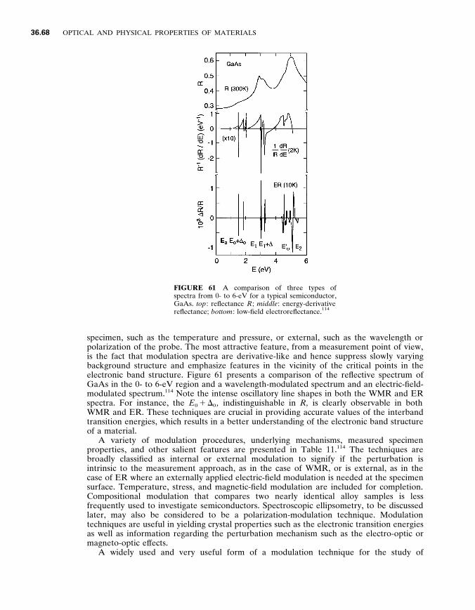
36 .68 OPTICAL AND PHYSICAL PROPERTIES OF MATERIALS
FIGURE 61 A comparison of three types of spectra from 0- to 6-eV for a typical semiconductor , GaAs . top : reflectance R ; middle : energy-derivative reflectance ; bottom : low-field electroreflectance . 1 1 4
specimen , such as the temperature and pressure , or external , such as the wavelength or polarization of the probe . The most attractive feature , from a measurement point of view , is the fact that modulation spectra are derivative-like and hence suppress slowly varying background structure and emphasize features in the vicinity of the critical points in the electronic band structure . Figure 61 presents a comparison of the reflective spectrum of GaAs in the 0- to 6-eV region and a wavelength-modulated spectrum and an electric-field- modulated spectrum . 1 1 4 Note the intense oscillatory line shapes in both the WMR and ER spectra . For instance , the E 0 1 D 0 , indistinguishable in R , is clearly observable in both WMR and ER . These techniques are crucial in providing accurate values of the interband transition energies , which results in a better understanding of the electronic band structure of a material .
A variety of modulation procedures , underlying mechanisms , measured specimen properties , and other salient features are presented in Table 11 . 1 1 4 The techniques are broadly classified as internal or external modulation to signify if the perturbation is intrinsic to the measurement approach , as in the case of WMR , or is external , as in the case of ER where an externally applied electric-field modulation is needed at the specimen surface . Temperature , stress , and magnetic-field modulation are included for completion . Compositional modulation that compares two nearly identical alloy samples is less frequently used to investigate semiconductors . Spectroscopic ellipsometry , to be discussed later , may also be considered to be a polarization-modulation technique . Modulation techniques are useful in yielding crystal properties such as the electronic transition energies as well as information regarding the perturbation mechanism such as the electro-optic or magneto-optic ef fects .
A widely used and very useful form of a modulation technique for the study of
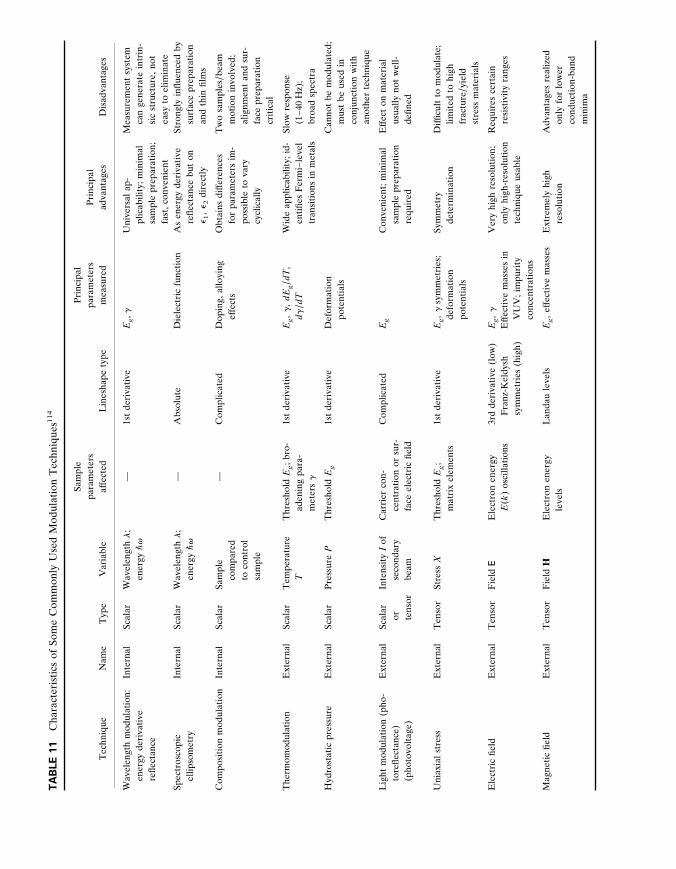
TA
BLE
11
Cha
ract
eris
tics
of
Som
e C
omm
only
Use
d M
odul
atio
n T
echn
ique
s 1 1 4
Tec
hniq
ue N
ame
Typ
e V
aria
ble
Sam
ple
para
met
ers
af fe
cted
Lin
esha
pe t
ype
Pri
ncip
al pa
ram
eter
s m
easu
red
Pri
ncip
al ad
vant
ages
Dis
adva
ntag
es
Wav
elen
gth
mod
ulat
ion :
ener
gy d
eriv
ativ
e re
flect
ance
Inte
rnal
Scal
ar W
avel
engt
h l
; en
ergy
" v
— 1s
t de
riva
tive
E g , g
Uni
vers
al a
p- pl
icab
ility
; min
imal
sam
ple
prep
arat
ion ;
fast
, con
veni
ent
Mea
sure
men
t sy
stem
can
gene
rate
int
rin-
sic
stru
ctur
e , n
ot ea
sy t
o el
imin
ate
Spec
tros
copi
c el
lipso
met
ry In
tern
al Sc
alar
Wav
elen
gth
l ;
ener
gy "
v
— A
bsol
ute
Die
lect
ric
func
tion
As
ener
gy d
eriv
ativ
e re
flect
ance
but
on
e 1 , e
2 di
rect
ly
Stro
ngly
infl
uenc
ed b
y su
rfac
e pr
epar
atio
n an
d th
in fi
lms
Com
posi
tion
mod
ulat
ion
Inte
rnal
Scal
ar Sa
mpl
e co
mpa
red
to c
ontr
ol sa
mpl
e
— C
ompl
icat
ed D
opin
g , a
lloyi
ng ef
fect
s O
btai
ns d
if fer
ence
s fo
r pa
ram
eter
s im
- po
ssib
le t
o va
ry cy
clic
ally
Tw
o sa
mpl
es / b
eam
mot
ion
invo
lved
; al
ignm
ent
and
sur-
face
pre
para
tion
crit
ical
The
rmom
odul
atio
n E
xter
nal
Scal
ar T
empe
ratu
re T
Thr
esho
ld E
g ; b
ro-
aden
ing
para
- m
eter
s g
1st
deri
vati
ve E
g , g
, dE
g / d
T ,
d g / d
T W
ide
appl
icab
ility
; id-
enti
fies
Fer
mi –
leve
l tr
ansi
tion
s in
met
als
Slow
res
pons
e (1
– 40
Hz)
; br
oad
spec
tra
Hyd
rost
atic
pre
ssur
e E
xter
nal
Scal
ar P
ress
ure
P T
hres
hold
E g
1st
deri
vati
ve D
efor
mat
ion
pote
ntia
ls C
anno
t be
mod
ulat
ed ;
mus
t be
use
d in
conj
unct
ion
wit
h an
othe
r te
chni
que
Lig
ht m
odul
atio
n (p
ho-
tore
flect
ance
) (p
hoto
volt
age)
Ext
erna
l Sc
alar
or tens
or
Inte
nsit
y I
of se
cond
ary
beam
Car
rier
con
- ce
ntra
tion
or
sur-
face
ele
ctri
c fie
ld
Com
plic
ated
E g
Con
veni
ent ;
min
imal
sam
ple
prep
arat
ion
requ
ired
Ef f
ect
on m
ater
ial
usua
lly n
ot w
ell-
defin
ed
Uni
axia
l st
ress
Ext
erna
l T
enso
r St
ress
X T
hres
hold
E g ;
mat
rix
elem
ents
1st
deri
vati
ve E
g , g
sym
met
ries
; de
form
atio
n po
tent
ials
Sym
met
ry de
term
inat
ion
Dif fi
cult
to
mod
ulat
e ; lim
ited
to
high
frac
ture
/ yie
ld st
ress
mat
eria
ls
Ele
ctri
c fie
ld E
xter
nal
Ten
sor
Fie
ld E
Ele
ctro
n en
ergy
E ( k
) os
cilla
tion
s 3r
d de
riva
tive
(lo
w)
Fra
nz-K
eldy
sh sy
mm
etri
es (
high
)
E g , g
E
f fec
tive
mas
ses
in V
UV
; im
puri
ty co
ncen
trat
ions
Ver
y hi
gh r
esol
utio
n ; on
ly h
igh-
reso
luti
on te
chni
que
usab
le
Req
uire
s ce
rtai
n re
sist
ivit
y ra
nges
Mag
neti
c fie
ld E
xter
nal
Ten
sor
Fie
ld H
Ele
ctro
n en
ergy
leve
ls L
anda
u le
vels
E g , e
f fec
tive
mas
ses
Ext
rem
ely
high
reso
luti
on A
dvan
tage
s re
aliz
ed on
ly f
or l
ower
cond
ucti
on-b
and
min
ima
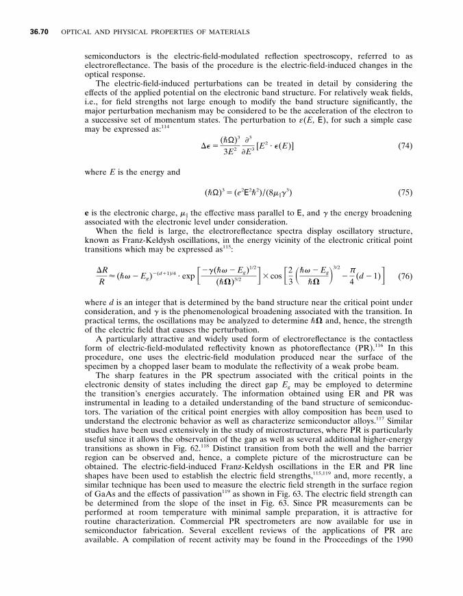
36 .70 OPTICAL AND PHYSICAL PROPERTIES OF MATERIALS
semiconductors is the electric-field-modulated reflection spectroscopy , referred to as electroreflectance . The basis of the procedure is the electric-field-induced changes in the optical response .
The electric-field-induced perturbations can be treated in detail by considering the ef fects of the applied potential on the electronic band structure . For relatively weak fields , i . e ., for field strengths not large enough to modify the band structure significantly , the major perturbation mechanism may be considered to be the acceleration of the electron to a successive set of momentum states . The perturbation to » ( E , E ) , for such a simple case may be expressed as : 1 1 4
D e 5 ( " Ω ) 3
3 E 2
3
E 3 [ E 2 ? e ( E )] (74)
where E is the energy and
( " Ω ) 3 5 ( e 2 E 2 " 2 ) / (8 m i g 3 ) (75)
e is the electronic charge , m i the ef fective mass parallel to E , and g the energy broadening associated with the electronic level under consideration .
When the field is large , the electroreflectance spectra display oscillatory structure , known as Franz-Keldysh oscillations , in the energy vicinity of the electronic critical point transitions which may be expressed as 1 1 5 :
(76) D R R
< ( " v 2 E g ) 2 ( d 1 1)/4 ? exp F 2 g ( " v 2 E g ) 1/2
( " V ) 3/2 G 3 cos F 2 3 S " v 2 E g
" V D 3/2
2 π 4
( d 2 1) G where d is an integer that is determined by the band structure near the critical point under consideration , and g is the phenomenological broadening associated with the transition . In practical terms , the oscillations may be analyzed to determine " V and , hence , the strength of the electric field that causes the perturbation .
A particularly attractive and widely used form of electroreflectance is the contactless form of electric-field-modulated reflectivity known as photoreflectance (PR) . 1 1 6 In this procedure , one uses the electric-field modulation produced near the surface of the specimen by a chopped laser beam to modulate the reflectivity of a weak probe beam .
The sharp features in the PR spectrum associated with the critical points in the electronic density of states including the direct gap E g may be employed to determine the transition’s energies accurately . The information obtained using ER and PR was instrumental in leading to a detailed understanding of the band structure of semiconduc- tors . The variation of the critical point energies with alloy composition has been used to understand the electronic behavior as well as characterize semiconductor alloys . 1 1 7 Similar studies have been used extensively in the study of microstructures , where PR is particularly useful since it allows the observation of the gap as well as several additional higher-energy transitions as shown in Fig . 62 . 1 1 8 Distinct transition from both the well and the barrier region can be observed and , hence , a complete picture of the microstructure can be obtained . The electric-field-induced Franz-Keldysh oscillations in the ER and PR line shapes have been used to establish the electric field strengths , 115 , 119 and , more recently , a similar technique has been used to measure the electric field strength in the surface region of GaAs and the ef fects of passivation 1 1 9 as shown in Fig . 63 . The electric field strength can be determined from the slope of the inset in Fig . 63 . Since PR measurements can be performed at room temperature with minimal sample preparation , it is attractive for routine characterization . Commercial PR spectrometers are now available for use in semiconductor fabrication . Several excellent reviews of the applications of PR are available . A compilation of recent activity may be found in the Proceedings of the 1990
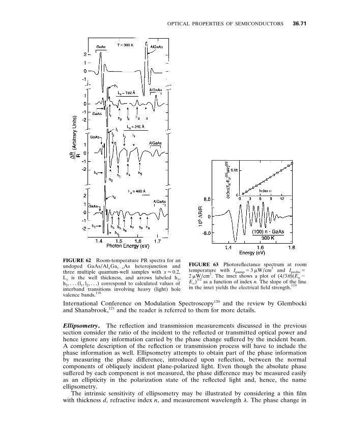
OPTICAL PROPERTIES OF SEMICONDUCTORS 36 .71
FIGURE 62 Room-temperature PR spectra for an undoped GaAs / Al x Ga 1 2 x As heterojunction and three multiple quantum-well samples with x < 0 . 2 , L z is the well thickness , and arrows labeled h 1 , h 2 , . . . (l 1 , l 2 , . . . ) correspond to calculated values of interband transitions involving heavy (light) hole valence bands . 1 1 8
FIGURE 63 Photoreflectance spectrum at room temperature with I pump 5 3 m W / cm 2 and I probe 5 2 m W / cm 2 . The inset shows a plot of (4 / 3 π )( E n 2 E o ) 3/2 as a function of index n . The slope of the line in the inset yields the electrical field strength . 1 1 9
International Conference on Modulation Spectroscopy 1 2 0 and the review by Glembocki and Shanabrook , 1 2 1 and the reader is referred to them for more details .
Ellipsometry . The reflection and transmission measurements discussed in the previous section consider the ratio of the incident to the reflected or transmitted optical power and hence ignore any information carried by the phase change suf fered by the incident beam . A complete description of the reflection or transmission process will have to include the phase information as well . Ellipsometry attempts to obtain part of the phase information by measuring the phase dif ference , introduced upon reflection , between the normal components of obliquely incident plane-polarized light . Even though the absolute phase suf fered by each component is not measured , the phase dif ference may be measured easily as an ellipticity in the polarization state of the reflected light and , hence , the name ellipsometry .
The intrinsic sensitivity of ellipsometry may be illustrated by considering a thin film with thickness d , refractive index n , and measurement wavelength l . The phase change in

36 .72 OPTICAL AND PHYSICAL PROPERTIES OF MATERIALS
the reflected component can be measured to a precision of 0 . 001 8 in ellipsometers which translates to a precision of , 10 2 5 l / 2 π n in thickness , i . e ., , 10 2 4 l ! or , 10 2 4 d / l in the refractive index . Such extraordinary precision may be used for the study of submonolayer films or as a real-time monitor for measuring very small changes in materials properties . The reader is referred to the chapter on ellipsometry 1 2 2 in this volume for more details .
Luminescence . The process of luminescence , as described earlier , occurs in a suitably excited specimen . It is a mechanism through which the excited specimen relaxes to the equilibrium state . 104 , 105 Hence , unlike reflection and transmission spectroscopies , lumines- cence procedures concentrate on the relaxation of the specimen and often lead to complementary information . For instance , impurities in semiconductors (particularly at low concentrations) are impossible to detect through reflection and more dif ficult to detect by absorption than by luminescence . Luminescence spectroscopy is thus an important part of the analysis of the optical behavior of semiconductors . 1 0 4 Moreover , since one of the main applications of semiconductors is in the arena of light emitters including lasers , the study of luminescence provides direct access to device optoelectronic information .
Luminescence processes may be induced by excitations that produce free electron-hole (e-h) pairs that may recombine across the band gap or through defect- and impurity- related intermediate steps and emit a photon . The excitations employed most often are : (1) an incident intense above band-gap radiation such as from a laser source ; (2) an incident electron beam ; (3) electrical injection of electrons and / or holes through an appropriate contact ; and (4) thermal excitation . These procedures are known as photoluminescence (PL) , cathodoluminescence (CL) , 1 2 3 electroluminescence (EL) , 1 2 4 and thermoluminescence (TL) , respectively . The most widely used technique for the analysis of semiconductor materials is PL . Cathodoluminescence measurements are usually conducted in a scanning electron microscope (SEM) . The SEM electron beam can be focused to a spot size , 1000 Å and can be scanned over the area of the sample . Hence , much work has been performed in CL imaging of wafers where one can obtain not only spectroscopic information but also spatial details . Electroluminescence is the most dif ficult to obtain because of the complexity of producing appropriate contacts . However , in terms of application , EL is the most important since a light emitter has to be able to produce light in an ef ficient manner under electrical excitation . Thermoluminescence is a technique used with insulators and wide-gap materials and not widely employed in the analysis of the commercially important materials such as GaAs and Si . The principles of luminescence and the optical information regarding the semiconductor that can be obtained are discussed in the next section using PL .
Photoluminescence . Luminescence processes may be excited using an above-band-gap beam of light that leads to the creation of an electron-hole pair (e-h) that may recombine across the gap and emit a photon with energy equal to the gap E g . This process is schematically displayed in Fig . 64 . 1 0 5 Two possibilities are shown : namely , the direct-gap and the indirect-gap semiconductors . The recombination will be direct in the former and will have to involve an additional participant , mostly a phonon , to conserve momentum in the latter . This is the simplest possible recombination mechanism . Several additional routes exist for the relaxation that involves impurities . The photoexcited charges may recombine with ionized acceptors (A) and donors (D) with or without involving a phonon . The process may also be more complicated where , for example , an electron may be trapped by an ionized donor which may subsequently recombine with a hole at a neutral acceptor , leading to a donor-acceptor pair (DAP) transition . In addition , recombination may also occur through the annihilation of excitons considered further in the following section .
Excitons , as discussed earlier , are hydrogen-like two-particle electron-hole combina- tions that are not included in the one-electron energy band description of the solid . The strong Coulomb interaction between the electron and the hole leads to the excitonic coupling .
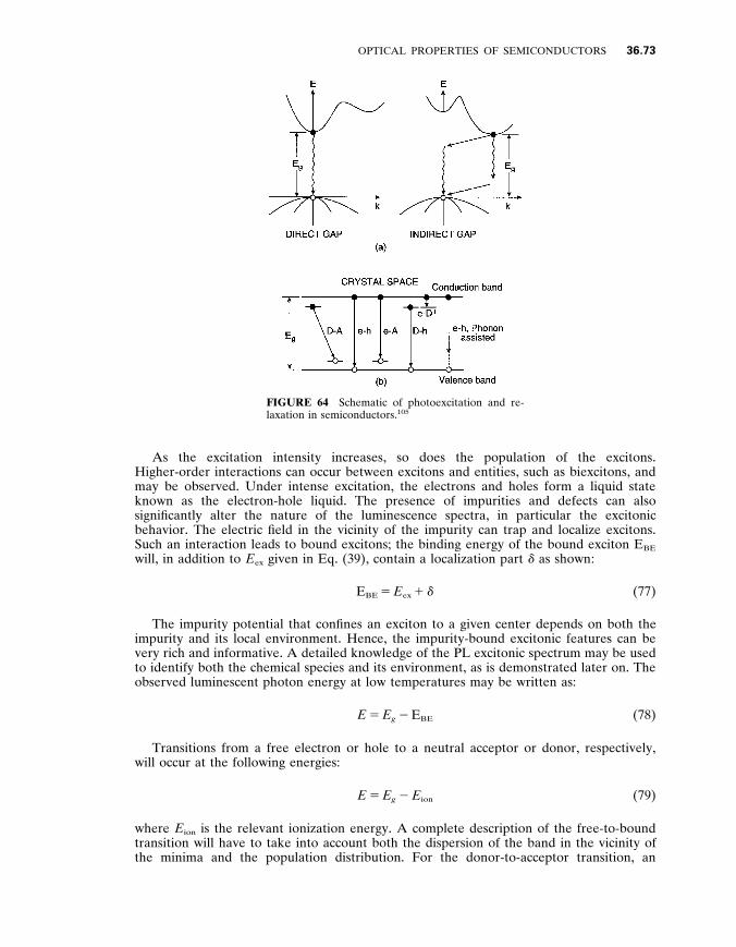
OPTICAL PROPERTIES OF SEMICONDUCTORS 36 .73
FIGURE 64 Schematic of photoexcitation and re- laxation in semiconductors . 1 0 5
As the excitation intensity increases , so does the population of the excitons . Higher-order interactions can occur between excitons and entities , such as biexcitons , and may be observed . Under intense excitation , the electrons and holes form a liquid state known as the electron-hole liquid . The presence of impurities and defects can also significantly alter the nature of the luminescence spectra , in particular the excitonic behavior . The electric field in the vicinity of the impurity can trap and localize excitons . Such an interaction leads to bound excitons ; the binding energy of the bound exciton E B E will , in addition to E e x given in Eq . (39) , contain a localization part d as shown :
E B E 5 E e x 1 d (77)
The impurity potential that confines an exciton to a given center depends on both the impurity and its local environment . Hence , the impurity-bound excitonic features can be very rich and informative . A detailed knowledge of the PL excitonic spectrum may be used to identify both the chemical species and its environment , as is demonstrated later on . The observed luminescent photon energy at low temperatures may be written as :
E 5 E g 2 E B E (78)
Transitions from a free electron or hole to a neutral acceptor or donor , respectively , will occur at the following energies :
E 5 E g 2 E ion (79)
where E ion is the relevant ionization energy . A complete description of the free-to-bound transition will have to take into account both the dispersion of the band in the vicinity of the minima and the population distribution . For the donor-to-acceptor transition , an
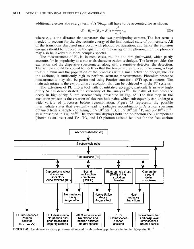
36 .74 OPTICAL AND PHYSICAL PROPERTIES OF MATERIALS
additional electrostatic energy term e 2 / e (0) r sep , will have to be accounted for as shown :
E 5 E g 2 ( E A 1 E D ) 1 e 2
e (0) r sep (80)
where r sep is the distance that separates the two participating centers . The last term is needed to account for the electrostatic energy of the final ionized state of both centers . All of the transitions discussed may occur with phonon participation , and hence the emission energies should be reduced by the quantum of the energy of the phonon ; multiple phonons may also be involved in more complex spectra .
The measurement of PL is , in most cases , routine and straightforward , which partly accounts for its popularity as a materials characterization technique . The laser provides the excitation and the dispersive spectrometer along with a sensitive detector , the detection . The sample should be cooled to , 5 K so that the temperature-induced broadening is kept to a minimum and the population of the processes with a small activation energy , such as the excitons , is suf ficiently high to perform accurate measurements . Photoluminescence measurements may also be performed using Fourier transform (FT) spectrometers . The main advantage is the extraordinary resolution that can be achieved with the FT systems .
The extension of PL into a tool with quantitative accuracy , particularly in very high- purity Si has demonstrated the versatility of the analysis . 1 2 5 The paths of luminescence decay in high-purity Si are schematically presented in Fig . 65 . The first step in the excitation process is the creation of electron-hole pairs , which subsequently can undergo a wide variety of processes before recombination . Figure 65 represents the possible intermediate states that eventually lead to radiative recombinations . A typical spectrum obtained from a sample containing 1 . 3 3 10 1 3 cm 2 3 B , 1 . 8 3 10 1 2 cm 2 3 P , and 3 3 10 1 1 cm 2 3 , as is presented in Fig . 66 . 1 2 5 The spectrum displays both the no-phonon (NP) component (shown as an inset) and TA , TO , and LO phonon-assisted features for the free exciton
FIGURE 65 Luminescence decay processes stimulated by above-bandgap photoexcitation in high-purity Si . 1 2 5

OPTICAL PROPERTIES OF SEMICONDUCTORS 36 .75
FIGURE 66 Photoluminescence spectrum from a Si sample doped with 1 . 3 3 10 1 3 cm 2 3 B , contaminated with 1 . 8 3 10 1 2 cm 2 3 P , and 3 3 10 1 1 cm 2 3 As . 1 2 5
(FE) and the impurity-related bound exciton features . The measurement was performed at 4 . 2 K . Since B is an acceptor and P and As are donors in Si , electrical transport analyses are not suf ficient to fully analyze the impurities . In contrast , all three impurities can be unambiguously identified using PL . In addition , when dependable calibration curves are available , the concentration of each species can also be established . A representative calibration curve is presented in Fig . 67 for the impurities B , Al , and P . 1 2 5 Note that quantitative measurements can be performed down to 10 1 2 cm 2 3 for all three impurities . In the case of B , in ultrapure samples , measurements can be performed to levels as low as , 10 1 0 cm 2 3 .
Next , we turn our attention to GaAs , which is a direct-band-gap material and hence exhibits ef ficient luminescence . Figure 68 a displays a representative spectrum from a high-quality MOCVD-grown sample doped with C and Zn measured using an FT spectrometer . 1 2 6 The spectra shown are intense , sharp , and well-resolved near the band edge , with excitonic features appearing slightly below the band gap of , 1 . 519 eV at 4 . 2 K . The near-edge features , labeled (A 0 , X) and (D 0 , X) , are due to excitons bound to neutral donors and acceptors , and the deeper-lying features are the free-to-bound transition to the
FIGURE 67 Calibration of the photoluminescence tech- nique for measuring B , P , and Al concentrations in Si . 1 2 5

36 .76 OPTICAL AND PHYSICAL PROPERTIES OF MATERIALS
FIGURE 68 a Representative PL spectrum from MOCVD-grown GaAs . 1 2 6
FIGURE 68 b High-resolution , near-band edge spec- trum of the same sample as in previous figure . 1 2 6
C acceptor , ( e , C 0 ) and the donor-acceptor-pair transitions , (D 0 , Zn 0 ) , and (D 0 , C 0 ) , to the Zn and C centers , respectively . An expanded high-resolution version of the same spectrum , in the vicinity of (A 0 , X) region , is displayed in Fig . 68 b . 1 2 6 Note the impressive resolution obtainable in the FT system and the clear resolution of the excited states associated with the bound exciton .
The use of PL techniques may be extended deeper in the infrared region as well . Deep levels associated with impurities such as Fe , Cr , and Ag in GaAs are known to produce luminescence bands at , 0 . 35 , , 0 . 6 , and , 1 . 2 eV . 1 2 7 The narrow-gap semiconductors such as InAs , InSb , and HgCdTe luminesce in the 100- to 200-meV region farther into the infrared region . An example of the PL spectra observed from Hg 0 . 78 Cd 0 . 22 Te narrow-gap alloy 1 2 8 is displayed in Fig . 69 . The spectra , in comparison to those presented earlier , are rather featureless due to the fact that the ef fective masses in the narrow-gap semiconduc- tors tend to be small , and hence the excitonic binding energies are small as well . Hence , sharp , well-resolved spectra are not normally observed . In addition , the Auger process , i . e ., nonradiative decay processes , is much stronger , making the observation of lumines- cence much more dif ficult in narrow-gap semiconductors .
The luminescence processes described provide information on the relaxation mecha- nisms and hence are heavily weighted towards transitions that involve only the first excited state and the final ground state of a system . A complete study of a recombination process , for instance , the FE , requires information regarding the higher excited states . This can be achieved by a variation of the PL procedure known as photoluminescence excitation (PLE) spectroscopy . The crux of this technique is to concentrate on the PL response with respect to the excitation wavelength and thereby to determine the excitation resonances . Since the resonances occur when the excitation photon energy matches the excited energies , information regarding the excited states may be elucidated . The principle is illustrated with Fig . 70 , where an attempt is made to determine the process that the photoexcited electron-hole pair undergoes before the formation of a free exciton in high-purity CdTe . 1 2 9 The spectrometer was set to the FE energy of 1 . 596 eV and the excitation photon energy was scanned from 1 . 6 to , 1 . 8 eV . The excitation wavelength may be scanned using a dye laser as shown in Fig . 70 . Two PLE spectra obtained at 1 . 8 and 20 . 6 K are displayed in Fig . 70 . The strong oscillatory behavior , with spacing of , 21 meV , demonstrates a cascade process through intermediate states separated by the LO phonon energy of 21 meV . This study illustrates the importance of the LO phonon in the
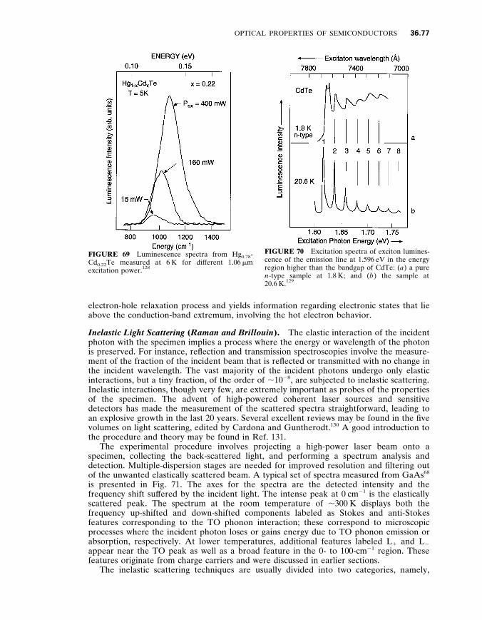
OPTICAL PROPERTIES OF SEMICONDUCTORS 36 .77
FIGURE 69 Luminescence spectra from Hg 0 . 78 - Cd 0 . 22 Te measured at 6 K for dif ferent 1 . 06 m m excitation power . 1 2 8
FIGURE 70 Excitation spectra of exciton lumines- cence of the emission line at 1 . 596 eV in the energy region higher than the bandgap of CdTe : ( a ) a pure n -type sample at 1 . 8 K ; and ( b ) the sample at 20 . 6 K . 1 2 9
electron-hole relaxation process and yields information regarding electronic states that lie above the conduction-band extremum , involving the hot electron behavior .
Inelastic Light Scattering ( Raman and Brillouin ) . The elastic interaction of the incident photon with the specimen implies a process where the energy or wavelength of the photon is preserved . For instance , reflection and transmission spectroscopies involve the measure- ment of the fraction of the incident beam that is reflected or transmitted with no change in the incident wavelength . The vast majority of the incident photons undergo only elastic interactions , but a tiny fraction , of the order of , 10 2 8 , are subjected to inelastic scattering . Inelastic interactions , though very few , are extremely important as probes of the properties of the specimen . The advent of high-powered coherent laser sources and sensitive detectors has made the measurement of the scattered spectra straightforward , leading to an explosive growth in the last 20 years . Several excellent reviews may be found in the five volumes on light scattering , edited by Cardona and Guntherodt . 1 3 0 A good introduction to the procedure and theory may be found in Ref . 131 .
The experimental procedure involves projecting a high-power laser beam onto a specimen , collecting the back-scattered light , and performing a spectrum analysis and detection . Multiple-dispersion stages are needed for improved resolution and filtering out of the unwanted elastically scattered beam . A typical set of spectra measured from GaAs 6 8
is presented in Fig . 71 . The axes for the spectra are the detected intensity and the frequency shift suf fered by the incident light . The intense peak at 0 cm 2 1 is the elastically scattered peak . The spectrum at the room temperature of , 300 K displays both the frequency up-shifted and down-shifted components labeled as Stokes and anti-Stokes features corresponding to the TO phonon interaction ; these correspond to microscopic processes where the incident photon loses or gains energy due to TO phonon emission or absorption , respectively . At lower temperatures , additional features labeled L 1 and L 2
appear near the TO peak as well as a broad feature in the 0- to 100-cm 2 1 region . These features originate from charge carriers and were discussed in earlier sections .
The inelastic scattering techniques are usually divided into two categories , namely ,
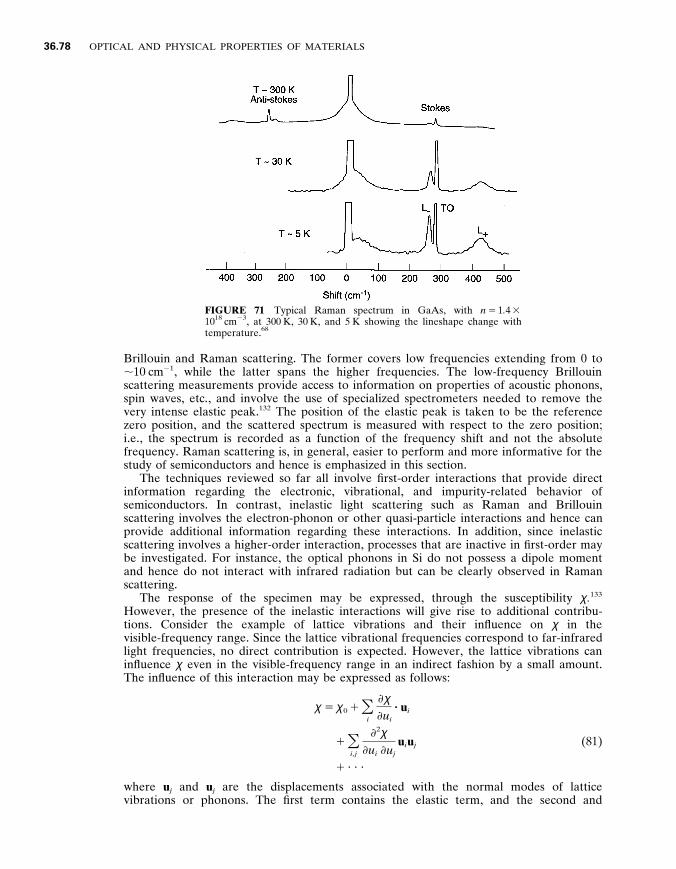
36 .78 OPTICAL AND PHYSICAL PROPERTIES OF MATERIALS
FIGURE 71 Typical Raman spectrum in GaAs , with n 5 1 . 4 3 10 1 8 cm 2 3 , at 300 K , 30 K , and 5 K showing the lineshape change with temperature . 6 8
Brillouin and Raman scattering . The former covers low frequencies extending from 0 to , 10 cm 2 1 , while the latter spans the higher frequencies . The low-frequency Brillouin scattering measurements provide access to information on properties of acoustic phonons , spin waves , etc ., and involve the use of specialized spectrometers needed to remove the very intense elastic peak . 1 3 2 The position of the elastic peak is taken to be the reference zero position , and the scattered spectrum is measured with respect to the zero position ; i . e ., the spectrum is recorded as a function of the frequency shift and not the absolute frequency . Raman scattering is , in general , easier to perform and more informative for the study of semiconductors and hence is emphasized in this section .
The techniques reviewed so far all involve first-order interactions that provide direct information regarding the electronic , vibrational , and impurity-related behavior of semiconductors . In contrast , inelastic light scattering such as Raman and Brillouin scattering involves the electron-phonon or other quasi-particle interactions and hence can provide additional information regarding these interactions . In addition , since inelastic scattering involves a higher-order interaction , processes that are inactive in first-order may be investigated . For instance , the optical phonons in Si do not possess a dipole moment and hence do not interact with infrared radiation but can be clearly observed in Raman scattering .
The response of the specimen may be expressed , through the susceptibility χ . 1 3 3
However , the presence of the inelastic interactions will give rise to additional contribu- tions . Consider the example of lattice vibrations and their influence on χ in the visible-frequency range . Since the lattice vibrational frequencies correspond to far-infrared light frequencies , no direct contribution is expected . However , the lattice vibrations can influence χ even in the visible-frequency range in an indirect fashion by a small amount . The influence of this interaction may be expressed as follows :
χ 5 χ 0 1 O i
χ u i
? u i
1 O i ,j
2 χ u i u j
u i u j (81)
1 ? ? ?
where u j and u j are the displacements associated with the normal modes of lattice vibrations or phonons . The first term contains the elastic term , and the second and
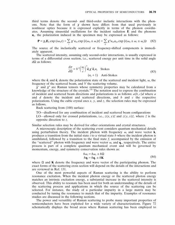
OPTICAL PROPERTIES OF SEMICONDUCTORS 36 .79
third terms denote the second- and third-order inelastic interactions with the phon- ons . Note that the form of χ shown here dif fers from that used previously in nonlinear optics because it is expressed explicitly in terms of the phonon coordin- ates . Assuming sinusoidal oscillations for the incident radiation E and the phonons u j , the polarization induced in the specimen may be expressed as follows :
P 5 χ 0 E 0 exp ( i v 0 t ) 1 O i
χ 9 u i 0 exp h i ( v 0 Ú v i ) t j 1 O ij
χ 0 u i 0 u j 0 exp h i ( v 0 Ú v i Ú v j ) j t (82)
The source of the inelastically scattered or frequency-shifted components is immedi- ately apparent .
The scattered intensity , assuming only second-order interactions , is usually expressed in terms of a dif ferential cross section , i . e ., scattered energy per unit time in the solid angle d Ω as follows :
(83)
d s
d Ω 5 V 2 S v s
c D 4
e i χ 9 e s n j Stokes
( n j 1 1) Anti-Stokes
where the e i and e s denote the polarization state of the scattered and incident light , v s the frequency of the scattered beam , and V the scattering volume .
χ 9 and χ 0 are Raman tensors whose symmetry properties may be calculated from a knowledge of the structure of the crystals . 1 3 4 The notation used to express the combination of incident and scattered beam directions and polarizations is as follows : a ( b , c ) d where a and d denote the incident and scattered directions , and b and c the respective polarizations . Using the cubic crystal axes x , y , and z , the selection rules may be expressed as follows .
Back scattering from (100) surface :
TO—disallowed for any combination of incident and scattered beam configurations LO—allowed only for crossed polarizations , i . e ., z ( x , y ) z # and z ( y , x ) z # , where z # is the opposite direction to z .
Similar selection rules may be derived for other orientations and crystal structures . A microscopic description of the scattering event considers quantum mechanical details
using perturbation theory . The incident photon with frequency v i and wave vector k i produces a transition from the initial state i to a virtual state b where the incident photon is annihilated , followed by a transition to the final state f , accompanied by the emission of the ‘‘scattered’’ photon with frequency and wave vector v s and q s , respectively . The entire process is part of a complete quantum mechanical event and will be governed by momentum , energy , and symmetry conservation rules shown as :
(84) " v i 5 " v s Ú " Ω " q i 5 " q s Ú " K
where Ω and K denote the frequency and wave vector of the participating phonon . The exact forms of the scattering cross section will depend on the details of the interactions and are reviewed in Ref . 131 .
One of the most powerful aspects of Raman scattering is the ability to perform resonance excitation . When the incident photon energy or the scattered photon energy matches an intrinsic excitation energy , a substantial increase in the scattered intensity is observed . This ability to resonate has been used for both an understanding of the details of the scattering process and applications in which the source of the scattering can be selected . For instance , the study of a particular impurity in a large matrix may be conducted by tuning the resonance to match that of the impurity . Examples of resonance studies are discussed in the following sections .
The power and versatility of Raman scattering to probe many important properties of semiconductors have been exploited for a wide variety of characterizations . Figure 72 schematically displays the broad areas where Raman scattering has been employed to

36 .80 OPTICAL AND PHYSICAL PROPERTIES OF MATERIALS
FIGURE 72 Schematics of inelastic light scattering and information which can be extracted from such mea- surements . 1 3 5
date . 1 3 5 The study of materials devices and microstructural properties include chemical , structural , and electronic properties . The developments in microscopic measurements and analysis have opened up new applications as well . The measurement of the temperature in a spot , 1 m m in diameter is one such example that is discussed in the following sections .
The most dominant Raman-scattering mechanism in semiconductors is that due to phonons—in particular , the optical phonons at the center of the Brillouin zone—namely , TO ( G ) and LO ( G ) . Even though a semiconductor crystal can support a variety of vibrations , the momentum conservation requirements restrict the interaction of the incident photon to only the TO ( G ) and LO ( G ) . The position and shape of the spectra contain important information regarding the structural state of the material : the presence of strain will be reflected as shifts in the line position ; degraded crystal quality due to multiple grains and concomitant distributed strain will lead to a broadening of the lineshape . The ef fects of crystal damage on the Raman spectrum as a result of ion implantation in GaAs is displayed in Fig . 73 . 1 3 6 Note the large increase in the linewidth of the LO ( G ) feature . In addition , a series of new structures , not present in the undamaged sample , can also be observed . These have been interpreted to be the result of relaxing the momentum conservation laws and hence the activation of phonon-scattering processes not normally allowed in a good crystal . A simple interpretation of the broadening of the LO lineshape was provided using a phonon confinement model , where the LO phonon is described as being confined to small damage-free regions . The shift in the position of the LO peak and the full-width-at-half-maximum were related to the diameter of the undamaged region . The information obtained is useful in characterizing lattice damage , amorphous materials , and degrees of recovery during annealing .
As explained earlier , Raman processes can involve higher-order interactions that involve more than one phonon . Hence , multiphonon scattering can be performed and information complementary to that discussed in the section entitled ‘‘Lattice’’ on the infrared absorption properties can be obtained . The Raman spectra obtained from Si 1 3 7 are

OPTICAL PROPERTIES OF SEMICONDUCTORS 36 .81
FIGURE 73 Raman spectra of k 100 l GaAs before implantation (A) , implanted to a fluence of 2 . 4 3 10 1 3 cm 2 2 for various polarization configurations (B , C , D , and E) and a fluence of 3 . 2 3 10 1 4 cm 2 2 (F) . 1 3 6
displayed in Fig . 74 . The spectra were recorded at room temperature where X 9 5 (100) , Y 9 5 (011) , and Z 9 5 (01 # 1) . The irreducible representation of the phonons involved is also noted in the figure . Note the strong peak at , 522 cm 2 1 which is due to the degenerate TO( G ) / LO( G ) phonons that are not observable in infrared absorption measurements . Additional bands present in the 200- to 400-cm 2 1 and the 600- to 1000-cm 2 1 range are due to multiphonon scattering processes . The ability to employ polarization selection rules has been used ef fectively to isolate the symmetry character of the underlying vibrational features and can be used to eventually identify the source of the various features . Such studies are useful in understanding both the optical behavior of Si and in illuminating the lattice dynamical properties of the material .
In crystals that contain a substantial number of free carriers , the incident photon can scatter of f collective charge oscillations , known as plasmons , discussed earlier . The Raman spectra measured from three GaAs samples 1 3 8 with electron densities ranging from 1 . 95 3 10 1 8 cm 2 3 to 6 . 75 3 10 1 8 cm 2 3 are presented in Fig . 75 . The observed features in addition to the LO phonon peak at , 293 cm 2 1 are due to the coupled LO phonon-plasmon features , also discussed earlier . The variation of the L 1 mode frequencies with the carrier density may be calculated and compared to measurements , as was shown in Fig . 34 . The shape of the L 1 and the L 2 features can be used to deduce the mobility of the carriers as well . The uniqueness of the Raman results is that they can be employed to study the behavior of carriers near the surface . Since the incident laser light with a photon energy of , 2 . 5 eV penetrates only , 1000 Å into the sample , the Raman results represent only the behavior of this near-surface region .
The single-particle nature of the free carriers can also be probed by Raman scattering . 6 8
The mechanism responsible for the interaction is the scattering of the carriers from inside the Fermi-surface to momentum states that lie outside , the total change in momentum being equal to that imparted by the photons . The integrated ef fect in the case of the spherical Fermi-surface in GaAs is displayed in Fig . 76 . The Fermi wave vector is denoted by p F and that of the electron is p . The wave-vector change as a result of the scattering is q .
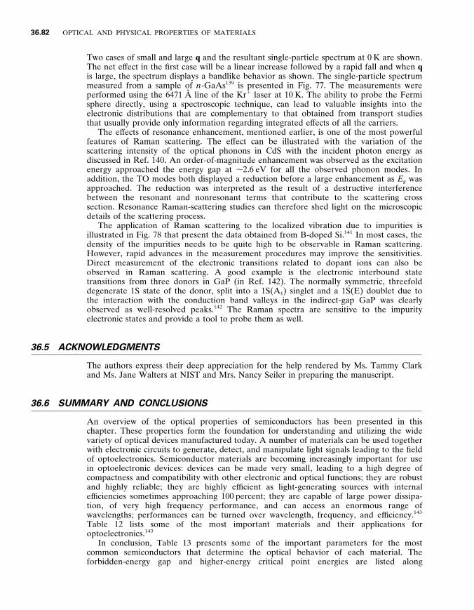
36 .82 OPTICAL AND PHYSICAL PROPERTIES OF MATERIALS
Two cases of small and large q and the resultant single-particle spectrum at 0 K are shown . The net ef fect in the first case will be a linear increase followed by a rapid fall and when q is large , the spectrum displays a bandlike behavior as shown . The single-particle spectrum measured from a sample of n -GaAs 1 3 9 is presented in Fig . 77 . The measurements were performed using the 6471 Å line of the Kr 1 laser at 10 K . The ability to probe the Fermi sphere directly , using a spectroscopic technique , can lead to valuable insights into the electronic distributions that are complementary to that obtained from transport studies that usually provide only information regarding integrated ef fects of all the carriers .
The ef fects of resonance enhancement , mentioned earlier , is one of the most powerful features of Raman scattering . The ef fect can be illustrated with the variation of the scattering intensity of the optical phonons in CdS with the incident photon energy as discussed in Ref . 140 . An order-of-magnitude enhancement was observed as the excitation energy approached the energy gap at , 2 . 6 eV for all the observed phonon modes . In addition , the TO modes both displayed a reduction before a large enhancement as E g was approached . The reduction was interpreted as the result of a destructive interference between the resonant and nonresonant terms that contribute to the scattering cross section . Resonance Raman-scattering studies can therefore shed light on the microscopic details of the scattering process .
The application of Raman scattering to the localized vibration due to impurities is illustrated in Fig . 78 that present the data obtained from B-doped Si . 1 4 1 In most cases , the density of the impurities needs to be quite high to be observable in Raman scattering . However , rapid advances in the measurement procedures may improve the sensitivities . Direct measurement of the electronic transitions related to dopant ions can also be observed in Raman scattering . A good example is the electronic interbound state transitions from three donors in GaP (in Ref . 142) . The normally symmetric , threefold degenerate 1S state of the donor , split into a 1S(A 1 ) singlet and a 1S(E) doublet due to the interaction with the conduction band valleys in the indirect-gap GaP was clearly observed as well-resolved peaks . 1 4 2 The Raman spectra are sensitive to the impurity electronic states and provide a tool to probe them as well .
3 6 . 5 ACKNOWLEDGMENTS
The authors express their deep appreciation for the help rendered by Ms . Tammy Clark and Ms . Jane Walters at NIST and Mrs . Nancy Seiler in preparing the manuscript .
3 6 . 6 SUMMARY AND CONCLUSIONS
An overview of the optical properties of semiconductors has been presented in this chapter . These properties form the foundation for understanding and utilizing the wide variety of optical devices manufactured today . A number of materials can be used together with electronic circuits to generate , detect , and manipulate light signals leading to the field of optoelectronics . Semiconductor materials are becoming increasingly important for use in optoelectronic devices : devices can be made very small , leading to a high degree of compactness and compatibility with other electronic and optical functions ; they are robust and highly reliable ; they are highly ef ficient as light-generating sources with internal ef ficiencies sometimes approaching 100 percent ; they are capable of large power dissipa- tion , of very high frequency performance , and can access an enormous range of wavelengths ; performances can be turned over wavelength , frequency , and ef ficiency . 1 4 3
Table 12 lists some of the most important materials and their applications for optoelectronics . 1 4 3
In conclusion , Table 13 presents some of the important parameters for the most common semiconductors that determine the optical behavior of each material . The forbidden-energy gap and higher-energy critical point energies are listed along
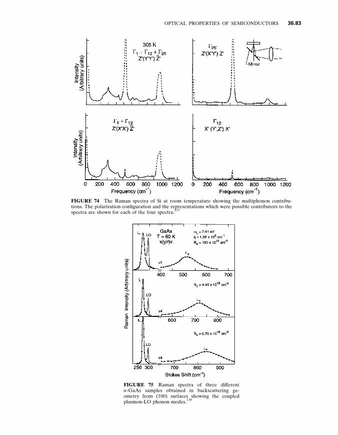
OPTICAL PROPERTIES OF SEMICONDUCTORS 36 .83
FIGURE 74 The Raman spectra of Si at room temperature showing the multiphonon contribu- tions . The polarization configuration and the representations which were possible contributors to the spectra are shown for each of the four spectra . 1 3 7
FIGURE 75 Raman spectra of three dif ferent n -GaAs samples obtained in backscattering ge- ometry from (100) surfaces showing the coupled plasmon-LO phonon modes . 1 3 8
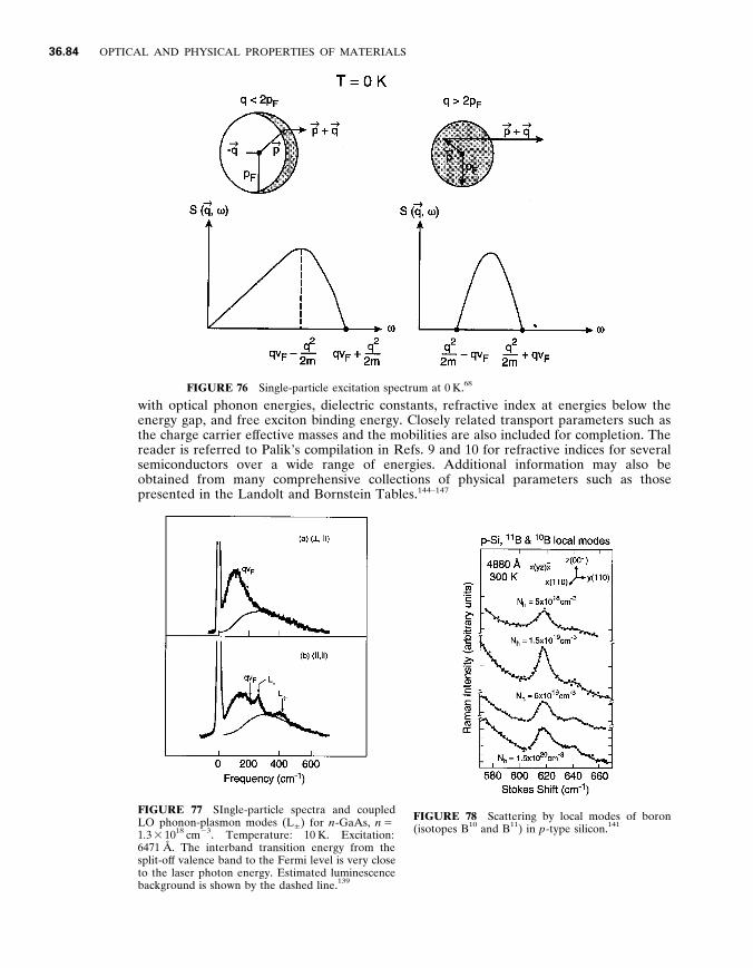
36 .84 OPTICAL AND PHYSICAL PROPERTIES OF MATERIALS
FIGURE 76 Single-particle excitation spectrum at 0 K . 6 8
with optical phonon energies , dielectric constants , refractive index at energies below the energy gap , and free exciton binding energy . Closely related transport parameters such as the charge carrier ef fective masses and the mobilities are also included for completion . The reader is referred to Palik’s compilation in Refs . 9 and 10 for refractive indices for several semiconductors over a wide range of energies . Additional information may also be obtained from many comprehensive collections of physical parameters such as those presented in the Landolt and Bornstein Tables . 144–147
FIGURE 77 SIngle-particle spectra and coupled LO phonon-plasmon modes (L
Ú ) for n -GaAs , n 5
1 . 3 3 10 1 8 cm 2 3 . Temperature : 10 K . Excitation : 6471 Å . The interband transition energy from the split-of f valence band to the Fermi level is very close to the laser photon energy . Estimated luminescence background is shown by the dashed line . 1 3 9
FIGURE 78 Scattering by local modes of boron (isotopes B 1 0 and B 1 1 ) in p -type silicon . 1 4 1

TA
BLE
12
Som
e Im
port
ant
Sem
icon
duct
or M
ater
ials
and
App
licat
ions
for
Opt
oele
ctro
nics
1 4 3
Mat
eria
l T
ype
Subs
trat
e D
evic
es
Wav
elen
gth
rang
e ( m
m)
App
licat
ions
Si IV
Si D
etec
tors
, sol
ar c
ells
0 . 5 –
1 So
lar
ener
gy c
onve
rsio
n , e
. g .,
wat
ches
, ca
lcul
ator
s , h
eati
ng , c
oolin
g , d
etec
tors
SiC
IV Si
C B
lue
LE
Ds
0 . 4
Dis
play
s , o
ptic
al d
isk
mem
orie
s , e
tc .
Ge
IV G
e D
etec
tors
1 – 1 .
8 Sp
ectr
osco
py G
aAs
III –
V G
aAs
LE
Ds ,
lase
rs , d
etec
tors
, sol
ar c
ells
, im
ager
s , i
nten
sifie
rs , e
lect
ro-o
ptic
mod
ulat
ors ,
opt
oiso
lato
rs
0 . 85
Rem
ote
cont
rol
TV
, etc
., vi
deo
disk
play
ers ,
ran
ge-fi
ndin
g , s
olar
ene
rgy
conv
ersi
on , o
ptic
al fi
ber
com
mun
icat
ion
syst
ems
(loc
al ne
twor
ks) ,
im
age
inte
nsifi
ers
AlG
aAs
III –
V G
aAs
LE
Ds ,
lase
rs , s
olar
cel
ls , i
mag
ers
0 . 67
– 0 . 9
8 G
aInP
III –
V G
aAs
Vis
ible
las
ers ,
LE
Ds
0 . 5 –
0 . 7
Dis
play
s , c
ontr
ol , c
ompa
ct d
isk
play
ers ,
lase
r pr
inte
rs / s
cann
ers ,
opt
ical
dis
k m
emor
ies ,
las
er m
edic
al e
quip
men
t G
aAlI
nP II
I – V
GaA
s V
isib
le l
aser
s , L
ED
s 0 .
5 – 0 .
7 G
aP II
I – V
GaP
Vis
ible
LE
Ds
0 . 5 –
0 . 7
GaA
sP II
I – V
GaP
Vis
ible
LE
Ds ,
opto
isol
ator
s 0 .
5 – 0 .
7 In
P II
I – V
InP
Sola
r ce
lls 0 .
9 Sp
ace
sola
r ce
lls In
GaA
s II
I – V
InP
Det
ecto
rs 1 –
1 . 67
Opt
ical
fibe
r co
mm
unic
atio
ns (
long
-hau
l an
d lo
cal
loop
) In
GaA
sP II
I – V
InP
Las
ers ,
LE
Ds
1 – 1 .
6 In
AlA
s II
I – V
InP
Las
ers ,
dete
ctor
s 1 –
2 . 5
InA
lGaA
s II
I – V
InP
Las
ers ,
dete
ctor
s 1 –
2 . 5
GaS
b / G
aAlS
b II
I – V
GaS
b D
etec
tors
, las
ers
2 – 3 .
5 Im
agin
g C
dHgT
e II
– VI
CdT
e IR
det
ecto
rs 3 –
5 an
d 8 –
12 In
frar
ed i
mag
ing ,
nig
ht v
isio
n si
ghts
, m
issi
le s
eeke
rs , a
nd m
any
othe
r m
ilita
ry a
pplic
atio
ns Z
nSe
II – V
I Z
nSe
Shor
t L
ED
, las
ers
0 . 4 –
0 . 6
Com
mer
cial
app
licat
ions
(R
&D
sta
ge on
ly)
ZnS
II – V
I Z
nS Sh
ort
LE
D , l
aser
s 0 .
4 – 0 .
6 P
b co
mpo
unds
IV – V
I P
b Com
poun
ds IR
las
ers ,
det
ecto
rs 3 –
30 Sp
ectr
osco
py , p
ollu
tion
mon
itor
ing
36 .85
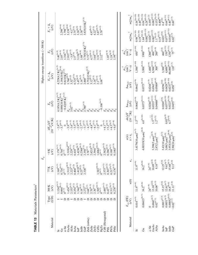
TA
BLE
13
Mat
eria
ls P
aram
eter
s 1
E g
Hig
her-
ener
gy t
rans
itio
ns (
, 30
0 K
)
Mat
eria
l T
ype
(I / D
) 30
0 K
(eV
) 77
K (e
V)
, 0
K (e
V)
dE g /
dT (1
0 2 4
eV / K
) E
0 (e
V)
E 0
1 D
0 (e
V)
E 1
(eV
) E
1 1
D 1
(eV
)
Si Ge
a -S
n G
aAs
AlA
s In
As
InP
InSb
I I D D I D D D
1 . 12
42 (a
-1)
0 . 66
4 (b-1
)
0 (c-1
)
1 . 42
4 (d-1
)
2 . 15
3 (e-1
)
0 . 35
4 (f-1
)
1 . 34
4 (g-1
)
0 . 18
(h-1
)
1 . 16
9 (a-1
)
0 . 73
4 (b-1
)
0 (c-1
)
1 . 51
15 (d
-2)
2 . 22
3 (e-1
)
0 . 40
4 (f-2
)
1 . 41
35 (g
-2)
0 . 23
(h-2
)
1 . 17
0 (a-1
)
0 . 74
4 (b-2
)
0 (c-1
)
1 . 51
914 (d
-3)
2 . 22
9 (e-1
)
0 . 41
8 (f-3
)
1 . 42
36 (g
-3)
0 . 23
68 (h
-2)
2 2 .
8 (a-2
)
2 3 .
7 (b-3
)
0 2
3 . 9 (d
-4)
2 3 .
6 (e-1
)
2 3 .
5 (f-4
)
2 2 .
9 (g-2
)
2 2 .
7 (h-2
)
4 . 18
5(4 .
2 K
) (a-3
)
0 . 88
8(10
K) (b
-4)
2 0 .
42(8
5 K
) (c-2
)
E g
3 . 02
(e-2
)
E g
E g
E g
4 . 22
9(4 .
2 K
) (a-3
)
1 . 18
4(10
K) (b
-4)
0 . 8(
10 K
) (c-2
)
1 . 76
0 (d-5
)
3 . 32
(e-2
)
0 . 72
5 (f-1
)
1 . 45
(g-4
)
1 . 16
(h-3
)
3 . 40
(a-4
)
2 . 05
(b-5
)
1 . 31
6 (c-3
)
2 . 91
5 d-6)
, 3 .
9 (e-2
)
2 . 5 (f
-5)
3 . 15
8 (g-5
)
1 . 88
(h-4
)
2 . 29
8 (b-6
)
1 . 79
8 (c-3
)
3 . 13
9 (d-6
)
, 4 .
1 (e-2
)
2 . 75
(f-5
)
3 . 28
(g-6
)
2 . 38
(h-4
)
GaP
ZnS
(cu
bic)
ZnS
e Z
nTe
CdT
e H
gTe
CdS
(H
exag
onal
) P
bS P
bTe
PbS
e
I D D D D D D D D D
2 . 27
2 (i-1
)
3 . 68
(j-1
)
2 . 70
(k-1
)
2 . 30
(l-1
)
1 . 50
5 (m-1
)
0 (n-1
)
2 . 48
5 (o-1
)
0 . 42
(p-1
)
0 . 31
1 (q-1
)
0 . 27
8 (r-1
)
2 . 33
8 (i-2
)
1 . 58
3 (m-2
)
0 (n-1
)
2 . 57
3 (o-1
)
0 . 30
7 (p-2
)
0 . 21
7 (q-2
)
0 . 17
6 (r-2
)
2 . 35
0 (i-1
)
3 . 78
(j-1
)
2 . 82
15 (k
-2)
2 . 39
41 (l
-2)
1 . 60
63 (m
-3)
0 (n-1
)
2 . 58
25 (o
-2)
0 . 28
6 (p-3
)
0 . 18
8 (q-1
)
0 . 14
63 (r
-3)
2 3 .
7 (i-2
)
2 4 .
7 (j-2
)
2 4 .
8 (k-3
)
2 4 .
1 (l-1
)
2 2 .
9 m-4
)
0 1
4 . 1 (o
-1)
1 5 .
2 (p-3
)
1 4 .
5 (q-3
)
1 4 .
0 (r-4
)
2 . 78
0 (i-3
)
E g
E g
E g
E g
2 0 .
106 (n
-1)
E g
E g
E g
E g
2 . 86
0 (i-3
)
3 . 75
2(15
K) (j
-3)
3 . 12
(k-1
)
3 . 18
(l-3
)
2 . 1 (m
-5)
1 . 08
(n-2
)
3 . 78
5(10
K) ( i
-3)
5 . 73
(j-1
)
4 . 77
(k-1
)
3 . 64
(l-3
)
3 . 31
(m-6
)
2 . 12
(n-2
)
1 . 85
(p-4
)
1 . 24
(q-4
)
1 . 59
(r-5
)
3 . 83
5(10
K) (i
-3)
4 . 97
(k-1
)
4 . 22
(l-3
)
3 . 87
(m-5
)
2 . 78
(n-2
)
Mat
eria
l E
e x (
FE
) (e
V)
e (0
) e
n ( l
) l
. l
c
dn / d
T (1
0 2 4 / K
) "
v T
O (e
V)
" v
L O
(eV
)
m e 2
(cm
2 / V
? s)
m h 2
(cm
2 / V
? s)
m * e /
m 0 7
m * h /
m 0 7
Si Ge
a -S
n G
aAs
AlA
s
InA
s In
P In
Sb G
aP
0 . 01
4 (a-5
)
0 . 00
415 (b
-7)
0 0 . 00
42 (d
-7)
0 . 02
(e-1
)
0 . 00
17 (f
-3)
0 . 00
51 (g
-3)
0 . 00
052 (h
-5)
, 0 .
02 (i
-1)
11 . 9
(a-6
)
16 . 2
(b-8
)
24 (c
-4)
13 . 1
8 (d-8
)
10 . 0
6 (e-3
)
15 . 1
5 (f-6
)
12 . 6
1 (g-7
)
16 . 8
(h-6
)
11 . 1
1 (i-4
)
11 . 9
(a-6
)
16 . 2
(b-8
)
24 (c
-4)
10 . 8
9 (d-8
)
8 . 16
(e-3
)
12 . 2
5 (f-6
)
9 . 61
(g-7
)
15 . 6
8 (h-7
)
9 . 11
(i-4
)
3 . 41
79(1
0 m
m) (a
-7)
4 . 00
319(
10 m
m) (b
-9)
— 3 .
298(
5 m
m) (d
-9)
2 . 87
(2 m
m) (e
-4)
3 . 42
(10
m m
) (f-7
)
3 . 08
(5 m
m) (g
-8)
3 . 95
3(10
m m
) (h-8
)
2 . 90
(10
m m
) (i-5
)
1 . 3 (a
-8)
4 . 0 (b
-10)
— 1 .
5 (d-1
0)
1 . 2 (e
-5)
0 . 83
(g-9
)
4 . 7 (h
-9)
0 . 06
42 (a
-9)
0 . 03
73 (b
-11)
0 . 02
44 (c
-5)
0 . 03
33 (d
-11)
0 . 04
488 (e
-6)
0 . 02
69 (f
-8)
0 . 03
77 (g
-10)
0 . 02
23 (h
-10)
0 . 04
55 (l
-6)
0 . 06
42 (a
-9)
0 . 03
73 (b
-11)
0 . 02
44 (c
-5)
0 . 03
62 (d
-11)
0 . 05
009 (e
-6)
0 . 02
96 (f
-8)
0 . 04
28 (g
-10)
0 . 02
37 (h
-10)
0 . 05
0 (i-6
)
1 , 50
0 (a-1
0)
3 , 90
0 (b-1
2)
1 , 40
0 (c-6
)
8 , 50
0 (d-1
2)
300 (e
-7)
3 , 30
0 (f-8
)
4 , 60
0 (g-1
1)
80 , 0
00 (h
-11)
110 (i
-7)
450 (a
-10)
1900
(b-1
2)
1200
(c-6
)
400 (d
-12)
200 (e
-8)
460 (f
-8)
150 (g
-11)
1250
(h-1
1)
75 (i
-7)
0 . 98
3 (a-1
0)
0 . 19
4 (a-1
0)
1 . 64
3 (b
-12)
0 . 08
2 4 (b
-13)
0 . 02
8 (c-2
)
0 . 06
7 (d-1
2)
1 . 1 3 (
e-2
)
0 . 19
4 (e-2
)
0 . 02
3 (f-8
)
0 . 07
7 (g-1
1)
0 . 01
45 (h
-11)
0 . 82
(i-7
)
0 . 16
5 (a-1
0)
0 . 49
6 (a-1
0)
0 . 04
5 (b
-12)
0 . 28
6 (b
-12)
0 . 19
5 (c-2
)
0 . 08
2 (d-1
2)
0 . 15
3 5 (e-9
)
0 . 40
9 6 (e-9
)
0 . 4 (f
-8)
0 . 64
(g-1
1)
0 . 40
(h-1
1)
0 . 60
(i-7
)

ZnS
(cu
bic)
ZnS
e Z
nTe
CdT
e H
gTe
CdS
(H
exag
onal
)
PbS
PbT
e
PbS
e
0 . 03
6 (j-4
)
0 . 01
8 (k-4
)
0 . 01
32 (l
-2)
0 . 01
05 (m
-3)
0 0 . 02
74 (o
-3)
5 . 1 (j
-5)
9 . 6 (k
-5)
10 . 1
(l-4
)
10 . 2
(m-7
)
21 . 0
(n-3
)
8 . 7(
e 1 1
(0))
(o-4
)
9 . 25
( e 3 3
(0))
(0-4
)
169 (p
-5)
414 (q
-5)
210 (r
-6)
2 . 95
(j-6
)
6 . 3 (k
-5)
7 . 28
(l-5
)
7 . 1 (m
-7)
15 . 2
(n-3
)
5 . 53
( e 1 1
) (o
-4)
5 . 5(
e 3 3
) (o
-4)
17 . 2
(p-5
)
33 (q
-6)
22 . 9
(r-7
)
2 . 20
14(1
0 m
m) (j
-7)
2 . 41
0(10
m m
) (k-6
)
2 . 64
(5 m
m) (1
-6)
2 . 68
4(5
m m
) (m-8
)
— 2 .
227(
10 m
m) '
c (0-5
)
2 . 24
5(10
m m
) i c (0
-5)
3 . 68
(16
m m
) (p-6
)
5 . 66
(10
m m
) (q-7
)
4 . 75
(10
m m
) (r-8
)
0 . 46
(j-8
)
0 . 52
(k-7
)
0 . 6 (0
-5)
0 . 62
(0-5
)
0 . 03
397 (j
-9)
0 . 02
542 (k
-8)
0 . 02
194 (l
-7)
0 . 01
74 (m
-7)
0 . 01
463 (n
-4)
See
(o-6
)
0 . 00
810 (p
-7)
0 . 00
399 (q
-5)
0 . 00
546 (r
-9)
0 . 04
364 (j
-10)
0 . 03
099 (k
-8)
0 . 02
542 (l
-7)
0 . 02
08 (m
-9)
0 . 01
71 (n
-4)
See
(o-6
)
0 . 02
539 (p
-7)
0 . 01
414 (q
-8)
0 . 01
65 (r
-10)
165 (j
-11)
600 (k
-9)
330 (l
-8)
1 , 05
0 (m-1
0)
35 , 0
00 (n
-5)
340 (o
-7)
600 (p
-8)
6 , 00
0 (q-9
)
1 , 00
0 (r-1
1)
5 (j-1
1)
100 (k
-10)
100 (m
-10)
50 (o
-7)
700 (p
-8)
4000
(q-9
)
800 (r
-12)
0 . 28
(j-1
2)
0 . 14
2 (k-1
1)
0 . 11
(1-9
)
0 . 1 (m
-11)
0 . 03
1 (n-6
)
0 . 21
(o-7
)
0 . 10
5 3 (p
-9)
0 . 08
0 4 p-9
)
0 . 24
3 (q
-10)
0 . 02
4 4 (q
-10)
0 . 07
3 (r-
13)
0 . 04
4 (r-
13)
0 . 49
(j-1
2)
0 . 57
(k-1
2)
0 . 6 (l
-10)
0 . 4 (m
-12)
0 . 42
(n-7
)
0 . 8 (o
-7)
0 . 10
5 3 (p
-9)
0 . 07
5 4 (p
-9)
0 . 31
3 (q
-10)
0 . 02
4 4 (q
-10)
0 . 06
8 3 (r-
13)
0 . 03
4 4 (r-
13)
1 M
ost
valu
es q
uote
d ar
e at
, 30
0 K
, exc
ept
whe
re i
ndic
ated
. 2
Hig
hest
val
ues
repo
rted
. 3
Lon
gitu
dina
l ef
fect
ive
mas
s . 4
Tra
nsve
rse
ef fe
ctiv
e m
ass .
5 L
ight
-hol
e ef
fect
ive
mas
s . 6
Hea
vy-h
ole
ef fe
ctiv
e m
ass .
7 B
and
extr
ema
ef fe
ctiv
e m
asse
s ar
e ob
tain
ed f
rom
low
-tem
pera
ture
mea
sure
men
ts . S
ee q
uote
d re
fere
nces
for
mor
e de
tails
.
a-Si (a
-1)
W . B
luda
u , A
. Ont
on , a
nd W
. Hei
nke ,
J .
App
l . P
hys .
45 :
1846
(19
74) .
(a-2
) H
. D . B
arbe
r , S
ol .
St .
Ele
ctro
nics
10 :
1039
(19
67) .
(a-3
) D
. E . A
spne
s an
d A
. A . S
tudn
a , S
olid
Sta
te C
omm
unic
atio
ns 1
1 : 13
75 (
1972
) . (a
-4)
A . D
uano
is a
nd D
. E . A
spne
s , P
hys .
Re y
. B
. 18 :
1824
(19
78) .
(a-5
) K
. L . S
hakl
ee a
nd R
. E . N
ahor
y , P
hys .
Re y
. L
ett .
24 : 9
42 (
1970
) . (a
-6)
K . V
. Rao
and
A . S
mak
ula ,
J .
App
l . P
hys .
37 :
2840
(19
66) .
(a-7
) C
. D . S
alzb
erg
and
J . J
. Vill
a , J
. O
pt .
Soc .
Am
. 47 :
244
(195
7) .
(a-8
) M
. Car
dona
, W . P
aul ,
and
H . B
rook
s , J
. P
hys .
Che
m .
Solid
s 8 :
204
(195
9) .
(a-9
) G
. Dol
ling ,
Ine
last
ic S
catte
ring
of
Neu
tron
s in
Sol
ids
and
Liq
uids
, vol
. II ,
IA
EA
, Vie
nna ,
196
3 , p
. 37 .
(a-1
0)
S . M
. Sze
, Phy
sics
of
Sem
icon
duct
or D
e y ic
es , 2
d ed
., Jo
hn W
iley ,
New
Yor
k , 1
981 ,
p . 8
49 .
b-G
e (b
-1)
G . G
. Mac
farl
ane ,
T . P
. McL
ean ,
J . E
. Qua
rina
ton ,
and
V . R
ober
ts , P
hys .
Re y
. 108
: 137
7 (1
957)
. (b
-2)
S . Z
wer
dlin
g , B
. Lax
, L . M
. Rot
h , a
nd K
. J . B
utto
n , P
hys .
Re y
. 114
: 80
(195
9) .
(b-3
) T
. P . M
cLea
n , i
n P
rogr
ess
in S
emic
ondu
ctor
s , v
ol . 5
, A . F
. Gib
son
(ed .
) , H
eyw
ood ,
Lon
don ,
196
0 . (b
-4)
D . E
. Asp
nes ,
Phy
s . R
e y .
B 1
2 : 22
97 (
1975
) . (b
-5)
A . K
. Gos
h , P
hys .
Re y
. 165
: 888
(19
68) .
(b-6
) L
. Vin
a an
d M
. Car
dona
, Phy
sica
117
B a
nd 1
18B
: 356
(19
83) .
(b-7
) V
. I . S
idor
ov a
nd Y
a . E
. Pok
rovs
ki , S
o y .
Phy
s . S
emic
ond
. 6 : 2
015
(197
3) .
(b-8
) F
. A . D
’Alt
roy
and
H . Y
. Fan
, Phy
s . R
e y . 1
03 : 1
671
(195
6) .
(b-9
) R
. P . E
dwin
, M . T
. Dud
erm
el , a
nd M
. Lam
are ,
App
l . O
pt . 2
1 : 87
8 (1
982)
. (b
-10)
See
(a-8
) . (b
-11)
G . N
ilsso
n an
d G
. Nel
in , P
hys .
Re y
. B
6 : 3
777
(197
2) .
(b-1
2)
See
(a-1
0) .

•‡
TA
BLE
13
Mat
eria
ls P
aram
eter
s ( C
ontin
ued
)
c- a
Sn (c
-1)
J . R
. Che
likow
sky
and
M . L
. Coh
en , P
hys .
Re y
. B
. 14 :
556
(197
6) .
(c-2
) S .
H . G
rove
s , C
. R . P
idge
on , A
. W . E
wal
d , a
nd R
. J . W
agne
r , J
. P
hys .
Che
m .
Solid
s 31
: 203
1 (1
970)
. (c
-3)
L . V
ina ,
H . H
ocks
t , an
d M
. Car
dona
, Phy
s . R
e y .
B 3
1 : 95
8 (1
985)
. (c
-4)
R . E
. Lin
dqui
st a
nd A
. W . E
wal
d , P
hys .
Re y
. 135
: A19
1 (1
964)
. (c
-5)
C . J
. Buc
hena
uer ,
M . C
ardo
na , a
nd F
. H . P
olla
k , P
hys .
Re y
. B
3 : 1
243
(197
1) .
(c-6
) Se
e (a
-10)
.
d-G
aAs
(d-1
) D
. D . S
ell ,
H . C
. Cas
ey , a
nd K
. W . W
echt
, J .
App
l . P
hys .
45 :
2650
(19
74) .
(d-2
) M
. B . P
anis
h an
d H
. C . C
asey
, J .
App
l . P
hys .
40 :
163
(196
9) .
(d-3
) B
. J . S
krom
me
and
G . E
. Sti
llman
, Phy
s . R
e y .
B 2
9 : 19
82 (
1984
) . (d
-4)
J . C
amas
sel ,
D . A
uver
gne ,
and
H . M
athi
eu , J
. A
ppl .
Phy
s . 4
6 : 26
83 (
1975
) . (d
-5)
C . A
liber
t , S .
Gai
llard
, M . E
rman
, and
P . M
. Fri
jlink
, J .
Phy
s . P
aris
44 :
C10
– 229
(19
83) .
(d-6
) P
. Lau
tens
chla
ger ,
M . G
arri
ga , S
. Log
othe
tidi
s , a
nd M
. Car
dona
, Phy
s . R
e y .
B 3
5 : 91
74 (
1987
) . (d
-7)
D . D
. Sel
l , P
hys .
Re y
. B
6 : 3
750
(197
2) .
(d-8
) G
. A . S
amar
a , P
hys .
Re y
. B
27 :
3494
(19
83) .
(d-9
) K
. G . H
ambl
eton
, C . H
ilsum
, and
B . R
. Hol
eman
, Pro
c . P
hys .
Soc
. 77 :
1147
(19
61) .
(d-1
0)
M . C
ardo
na , P
roc .
Int
. C
onf .
Phy
s . S
emic
ond .
, Pra
gue ,
196
0 , P
ubl .
Hou
se o
f th
e C
zech
. Aca
d . o
f Sc
ienc
es , P
ragu
e , 1
960 ,
p . 3
88 .
(d-1
1)
A . M
oora
dian
and
G . B
. Wri
ght ,
Solid
Sta
te C
omm
unic
atio
ns 4
: 431
(19
66) .
(d-1
2)
See
(a-1
0) .
e-A
lAs
(e-1
) B
. Mon
emar
, Phy
s . R
e y .
B 8
: 571
1 (1
983)
. (e
-2)
S . A
dach
i , J .
App
l . P
hys .
58 :
R1
(198
5) .
(e-3
) R
. E . F
ern
and
A . O
nton
, J .
App
l . P
hys .
42 :
3499
(19
71) .
(e-4
) M
. Hoc
h an
d K
. S . H
inge
, J .
Che
m .
Phy
s . 3
5 : 45
1 (1
961)
. (e
-5)
H . G
. Gri
mm
eiss
and
B . M
onem
ar , P
hys .
Sta
t . So
l . ( a
) 5 :
109
(197
1) .
(e-6
) O
. K . K
im a
nd W
. G . S
pitz
er , J
. A
ppl .
Phy
s . 5
0 : 43
62 (
1979
) . (e
-7)
M . E
tten
berg
, A . G
. Sig
ai , A
. Dre
eben
, and
S . L
. Gilb
ert ,
J . E
lect
roch
em .
Soc .
119
: 135
5 (1
971)
. (e
-8)
J . D
. Wile
y , i
n Se
mic
ondu
ctor
s an
d Se
mim
etal
s , v
ol . 1
0 , R
. K . W
illar
dson
and
A . C
. Bee
r (e
ds . )
, Aca
dem
ic P
ress
, New
Yor
k , 1
975 ,
p . 9
1 . (e
-9)
M . H
uang
and
W . Y
. Chi
ng , J
. P
hys .
Che
m .
Solid
s 46
: 977
(19
85) .
f-In
As
(f-1
) F
. Luk
es , P
hys .
Sta
t . So
l . ( b
) 84
: K11
3 (1
977)
. (f
-2)
E . A
dach
i , J .
Phy
s . S
oc .
Jpn
. 2 : 1
178
(196
8) .
(f-3
) A
. V . V
arfo
lom
eev ,
R . P
. Sei
syan
, and
R . N
. Yak
imov
a , S
o y .
Phy
s . S
emic
ond
. 9 : 5
60 (
1975
) . (f
-4)
F . M
atos
si a
nd F
. Ste
rn , P
hys .
Re y
. 111
: 472
(19
58) .
(f-5
) M
. Car
dona
and
G . H
arbe
ke , J
. A
ppl .
Phy
s . 3
4 : 81
3 (1
963)
. (f
-6)
M . H
aas
and
B . W
. Hen
vis ,
J .
Phy
s . C
hem
. So
lids
23 : 1
099
(196
2) .
(f-7
) O
. G . L
orim
or a
nd W
. G . S
pitz
er , J
. A
ppl .
Phy
s . 3
6 : 18
41 (
1965
) . (f
-8)
R . C
arle
s , N
. Sai
nt-C
ricq
, J . B
. Ren
ucci
, M . A
. Ren
ucci
, and
A . Z
wic
k , P
hys .
Re y
. B
22 :
4804
(19
80) .
g-In
P (g
-1)
M . B
ugas
ki a
nd W
. Lew
ando
wsk
i , J .
App
l . P
hys .
57 :
521
(198
5) .
(g-2
) W
. J . T
urne
r , W
. E . R
eese
, and
G . D
. Pet
tit ,
Phy
s . R
e y . 1
36 : A
1467
(19
64) .
(g-3
) H
. Mat
hieu
, Y . C
hen ,
J . C
amas
sel ,
J . A
llegr
e , a
nd D
. S . R
ober
tson
, Phy
s . R
e y .
B 3
2 : 40
42 (
1985
) . (g
-4)
K . L
. Sha
klee
, M . C
ardo
na , a
nd F
. H . P
olla
k , P
hys .
Re y
. L
ett .
16 : 4
8 (1
966)
. (g
-5)
S . M
. Kel
so , D
. E . A
spne
s , M
. A . P
olla
k , a
nd R
. E . N
ahor
y , P
hys .
Re y
. B
26 :
6669
(19
82) .
(g-6
) E
. Mat
atag
ui , A
. E . T
hom
pson
, and
M . C
ardo
na , P
hys .
Re y
. 176
: 950
(19
68) .
(g-7
) Se
e (f
-6) .
(g-8
) F
. Osw
ald ,
Z .
Nat
urfo
rsch
9a :
181
(195
4) .
(g-9
) Se
e (d
-10)
. (g
-10)
A . M
oora
dian
and
G . B
. Wri
ght ,
Solid
Sta
te C
omm
unic
atio
ns 4
: 431
(19
66) .
(g-1
1)
See
(a-1
0) .
h-In
Sb (h
-1)
F . L
ukes
and
E . S
chm
idt ,
Pro
c . I
nt .
Con
f . P
hys .
Sem
icon
d . , E
xete
r , 1
962 ,
Ins
t . of
Phy
sics
, Lon
don ,
196
2 , p
. 389
. (h
-2)
C . L
. Lit
tler
and
D . G
. Sei
ler ,
App
l . P
hys .
Let
t . 46
: 986
(19
85) .
(h-3
) S .
Zw
erdl
ing ,
W . H
. Kle
iner
, and
J . P
. The
riau
lt , M
IT L
inco
ln L
abor
ator
y R
epor
t 8 G
- 0 0 M
, 196
1 . (h
-4)
M . C
ardo
na , K
. L . S
hakl
ee , a
nd F
. H . P
olla
k , P
hys .
Re y
. 154
: 696
(19
67) .
(h-5
) A
. Bal
dere
schi
and
N . O
. Lip
ari ,
Phy
s . R
e y .
B 3
: 439
(19
71) .
(h-6
) J .
R . D
ixon
and
J . K
. Fur
dyna
, Sol
id S
tate
Com
mun
icat
ions
35 :
195
(198
0) .
(h-7
) Se
e (f
-6) .
(h-8
) T
. S . M
oss ,
S . D
. Sm
ith ,
and
T . D
. F . H
awki
ns , P
roc .
Phy
s . S
oc .
B 7
0 : 77
6 (1
957)
. (h
-9)
See
(g-9
) . (h
-10)
W . K
eife
r , W
. Ric
hter
, and
M . C
ardo
na , P
hys .
Re y
. B
12 :
2346
(19
75) .
(h-1
1)
See
(a-1
0) .
i-G
aP (i-1
) R
. G . H
umph
reys
, U . R
ossl
er , a
nd M
. Car
dona
, Phy
s . R
e y .
B 1
8 : 55
90 (
1978
) . (i
-2)
D . A
uver
gne ,
P . M
erle
, and
H . M
athi
eu , P
hys .
Re y
. B
12 :
1371
(19
75) .
(i-3
) S .
E . S
toko
wsk
i an
d D
. D . S
ell ,
Phy
s . R
e y .
B 5
: 163
6 (1
972)
. (i
-4)
G . A
. Sam
ara ,
Phy
s . R
e y .
B 2
7 : 34
94 (
1983
) . (i
-5)
H . W
elke
r , J
. E
lect
ron
1 : 18
1 (1
955)
. (i
-6)
See
(g-1
0) .
(i-7
) Se
e (a
-10)
.
j-Z
nS (j-1
) D
. The
is , P
hys .
Sta
t . So
l . ( b
) 79
: 125
(19
77) .
(j-2
) J .
Cam
asse
l an
d D
. Auv
ergn
e , P
hys .
Re y
. B
12 :
3258
(19
75) .
(j-3
) B
. Seg
all
and
D . T
. F . M
arpl
e , P
hysi
cs a
nd C
hem
istr
y of
II -
VI
Com
poun
ds , M
. Ave
n an
d J .
S . P
rene
r (e
ds . )
, Nor
th-H
olla
nd , A
mst
erda
m , 1
967 ,
p . 3
18 .
(j-4
) W
. Wal
ter
and
J . L
. Bir
man
, Pro
c . I
nt .
Con
f . o
n II
- VI
Sem
icon
duct
ing
Com
poun
ds , 1
9 6 7 ,
D . G
. Tho
mas
(ed
. ) , W
. A . B
enja
min
, New
Yor
k , 1
967 ,
p . 8
9 . (j
-5)
G . M
arti
nez ,
in
Han
dboo
k on
Sem
icon
duct
ors ,
vol
. 2 , T
. S . M
oss
(ed .
) , N
orth
-Hol
land
, Am
ster
dam
, 198
0 , p
. 210
. (j
-6)
M . B
alka
nski
and
Y . P
etro
f f , P
roc .
7 th
Int
l . C
onf .
Phy
sics
of
Sem
icon
d . P
aris
, 196
4 , D
unod
, Par
is , 1
964 ,
p . 2
45 .
(j-7
) W
. L . W
olfe
, A . G
. DeB
ell ,
and
J . M
. Pal
mer
, Pro
c . S
PIE
245
: 164
(19
80) .
(j-8
) R
. J . H
arri
s , G
. T . J
ohns
ton ,
G . A
. Kep
ple ,
P . C
. Kro
ck , a
nd M
. Muk
ai , A
ppl .
Opt
. 16 :
436
(197
7) .
(j-9
) M
. Bal
kans
ki , M
. Nus
imov
ici ,
and
R . L
etou
llec ,
J .
Phy
s . P
aris
25 :
305
(196
4) .
(j-1
0)
C . A
. Kle
in a
nd R
. N . D
onad
io , J
. A
ppl .
Phy
s . 5
1 : 79
7 (1
980)
. (j
-11)
See
(a-1
0) .
(j-1
2)
J . C
. Mik
losz
and
R . G
. Whe
eler
, Phy
s . R
e y . 1
53 : 9
13 (
1967
) .

•
‡TA
BLE
13
Mat
eria
ls P
aram
eter
s ( C
ontin
ued
)
k-Z
nSe
(k-1
) Se
e (j
-1) .
(k-2
) P
. J . D
ean ,
D . C
. Her
bert
, C . J
. Wer
khov
en , B
. J . F
itzp
atri
ck , a
nd R
. M . B
harg
ava ,
Phy
s . R
e y .
B 2
3 : 48
88 (
1981
) . (k
-3)
J . B
aillo
u , J
. Dau
nay ,
P . B
ugne
t , Ja
c D
auna
y , C
. Auz
ary ,
and
P . P
oind
essa
ult ,
J . P
hys .
Che
m .
Solid
s 41
: 295
(19
80) .
(k-4
) A
. K . R
ay a
nd F
. A . K
roge
r , J
. A
ppl .
Phy
s . 5
0 : 42
08 (
1979
) . (k
-5)
A . H
adni
, J . C
laud
el , a
nd P
. Str
imer
, Phy
s . S
tat .
Sol .
26 : 2
41 (
1968
) . (k
-6)
X . J
. Jia
ng , T
. His
amur
a , Y
. Nos
ua , a
nd T
. Got
o , J
. P
hys .
Soc
. Jp
n 52
: 400
8 (1
983)
. (k
-7)
See
(j-8
) . (k
-8)
M . C
ardo
na , J
. P
hys .
Par
is C
8 : 29
(19
84) .
(k-9
) T
. Yao
, M . O
gura
, S . M
atsu
oka ,
and
T . M
oris
hita
, J .
App
l . P
hys .
43 :
499
(198
3) .
(k-1
0)
G . J
ones
and
J . W
oods
, J .
Phy
s . D
9 : 7
99 (
1976
) . (k
-11)
T . O
hyam
a , E
. Ots
uka ,
T . Y
oshi
da , M
. Iss
hiki
, and
K . I
gaki
, Jpn
. J .
App
l . P
hys .
23 :
L38
2 (1
984)
. (k
-12)
M . S
onde
rgel
d , P
hys .
Sta
. So
l . ( b
) 81
: 253
(19
77) .
l-Z
nTe
(l-1
) Se
e (j
-1) .
(l-2
) M
. Ven
ghau
s an
d P
. J . D
ean ,
Phy
s . R
e y .
B 2
1 : 15
96 (
1980
) . (l
-3)
See
(h-5
) . (l
-4)
D . B
erlin
cour
t , M
. Jaf
fe , a
nd L
. R . S
hioz
awa ,
Phy
s . R
e y . 1
29 : 1
009
(198
3) .
(l-5
) D
. T . F
. Mar
ple ,
J .
App
l . P
hys .
35 :
539
(196
4) .
(l-6
) T
. L . C
hu , S
. S . C
hu , F
. Fir
szt ,
and
C . H
erri
ngto
n , J
. A
ppl .
Phy
s . 5
9 : 12
59 (
1986
) . (l
-7)
See
(k-8
) . (l
-8)
A . G
. Fis
her ,
J . N
. Car
ides
, and
J . D
resn
er , S
olid
Sta
te C
omm
un . 2
: 157
(19
64) .
(l-9
) H
. Ven
ghau
s , P
. J . D
ean ,
P . E
. Sim
mon
ds , a
nd J
. C . P
fiste
r , Z
. P
hys .
B 3
0 : 12
5 (1
978)
. (l
-10)
M . A
ven
and
B . S
egal
l , P
hys .
Re y
. 130
: 81
(196
3) .
m-C
dTe
(m-1
) P
. M . A
mir
thar
aj a
nd D
. Cha
ndle
r-H
orow
itz ,
(to
be
publ
ishe
d) .
(m-2
) P
. M . A
mir
thar
aj , R
. C . B
owm
an , J
r ., a
nd R
. L . A
lt , P
roc .
SP
IE 9
46 : 5
7 (1
988)
. (m
-3)
N . N
awro
cki
and
A . T
war
dow
ski ,
Phy
s . S
tat .
Sol .
( b )
97 : K
61 (
1980
) . (m
-4)
See
(j-2
) . (m
-5)
See
(l-3
) . (m
-6)
A . M
orit
ani ,
K . T
amig
uchi
, C . H
amag
uchi
, and
J . N
akai
, J .
Phy
s . S
oc .
Jpn
. 34 :
79 (
1973
) . (m
-7)
T . J
. Par
ker ,
J . R
. Bir
ch , a
nd C
. L . M
ok , S
olid
Sta
te C
omm
unic
atio
ns 3
6 : 58
1 (1
980)
. (m
-8)
L . S
. Lad
d , I
nfra
red
Phy
s . 6
: 145
(19
66) .
(m-9
) J .
R . B
irch
and
D . K
. Mur
ray ,
Inf
rare
d P
hys .
18 :
283
(197
8) .
(m-1
0)
See
(a-1
0) .
(m-1
1)
K . K
. Kan
azaw
a an
d F
. C . B
row
n , P
hys .
Re y
. 135
: A17
57 (
1964
) . (m
-12)
See
(j-3
) .
n-H
gTe
(n-1
) W
. Szu
szki
ewic
z , P
hys .
Sta
t . So
l . ( b
) 81
: K11
9 (1
977)
. (n
-2)
See
(m-6
) . (n
-3)
J . B
aars
and
F . S
orge
r , S
olid
Sta
te C
omm
un . 1
0 : 87
5 (1
972)
. (n
-4)
H . K
epa ,
T . G
iebu
ltow
icz ,
B . B
uras
, B . L
ebec
h , a
nd K
. Cla
usen
, Phy
sica
Scr
ipta
25 :
807
(198
2) .
(n-5
) T
. C . H
arm
on , i
n P
hysi
cs a
nd C
hem
istr
y of
II -
VI
Com
poun
ds , M
. Ave
n an
d J .
S . P
rene
r (e
ds) ,
Nor
th H
olla
nd P
ublis
hing
, Am
ster
dam
, 196
7 , p
. 767
. (n
-6)
Y . G
uldn
er , C
. Rig
aux ,
M . G
rynb
erg ,
A . M
ycie
lski
, Phy
s . R
e y .
B 8
: 387
5 (1
973)
. (n
-7)
K . S
hini
zu , S
. Nar
ita ,
Y . N
isid
a , a
nd V
. I . I
vano
v-O
msk
ii , S
olid
Sta
te C
omm
un . (
eds .
) , 3
2 : 32
7 (1
979)
.

o-C
dS (o
-1)
V . V
. Sob
olev
, V . I
. Don
etsk
ina ,
and
E . F
. Zag
aino
v , S
o y .
Phy
s . S
emic
ond
. 12 :
646
(197
8) .
(o-2
) D
. G . S
eile
r , D
. Hei
man
, and
B . S
. Whe
rret
t , P
hys .
Re y
. B
27 :
2355
(19
83) .
(o-3
) A
ser
ies
exci
tons
: D
. G . S
eile
r , D
. Hei
man
, R . F
iege
nbla
tt , R
. Agg
arw
al , a
nd B
. Lax
, Phy
s . R
e y .
B 2
5 : 76
66 (
1982
) ; B
ser
ies
exci
tons
: se
e (o
-2) .
(o-4
) A
. S . B
arke
r an
d C
. J . S
umm
ers ,
J .
App
l . P
hys .
41 :
3552
(19
70) .
(o-5
) R
. Wei
l an
d D
. Nes
hmit
, J .
Opt
. So
c . A
m . 6
7 : 19
0 (1
977)
. (o
-6)
Com
plex
Pho
non
Stru
ctur
e w
ith
Nin
e A
llow
ed O
ptic
al M
odes
. See
B . T
el , T
. C . D
amen
, and
S . P
. S . P
orto
, Phy
s . R
e y . 1
44 : 7
71 (
1966
) . (o
-7)
See
(a-1
0) .
p-P
bS (p
-1)
R . B
. Sch
oola
r an
d J .
R . D
ixon
, Phy
s . R
e y .
A 1
37 : 6
67 (
1965
) . (p
-2)
D . L
. Mit
chel
l , E
. D . P
alik
, and
J . N
. Zem
el , P
roc .
7 th
Int
. C
onf .
Phy
s . S
emic
ond .
, Par
is , 1
964 ,
Dun
od , P
aris
, 196
4 , p
. 325
. (p
-3)
G . N
imtz
and
B . S
chlic
ht , S
prin
ger
Tra
cts
in M
oder
n P
hysi
cs , v
ol . 9
8 , S
prin
ger-
Ver
lag ,
Ber
lin , 1
983 ,
p . 1
. (p
-4)
M . C
ardo
na a
nd D
. L . G
reen
away
, Phy
s . R
e y .
A 1
33 : 1
685
(196
4) .
(p-5
) R
. Dal
ven ,
in
Solid
Sta
te P
hysi
cs , v
ol . 2
8 , H
. Ehr
enre
ich ,
F . S
eitz
, and
D . T
urnb
ull
(eds
. ) , A
cade
mic
, NY
, 197
3 , p
. 179
. (p
-6)
R . B
. Sch
oola
r an
d J .
N . Z
emel
, J .
App
l . P
hys .
35 :
184
8 (1
964)
. (p
-7)
M . M
. Elc
ombe
, Pro
c . S
oc .
Lon
don
, A30
0 : 21
0 (1
967)
. (p
-8)
See
(a-1
0) .
(p-9
) K
. F . C
uf f ,
M . R
. Elle
t , C
. D . K
ulgi
n , a
nd L
. R . W
illia
ms ,
in
Pro
c . 7
th I
nt .
Con
f . P
hys .
Sem
icon
d . ,
Par
is , 1
964 ,
M . H
ulin
(ed
. ) , D
unod
, Par
is , 1
964 ,
p . 6
77 .
q-P
bTe
(q-1
) M
. Pre
ier ,
App
l . P
hys .
20 :
189
(197
9) .
(q-2
) C
. R . H
ewes
, M . S
. Adl
er , a
nd S
. D . S
entu
ria ,
Phy
s . R
e y .
B 7
: 519
5 (1
973)
. (q
-3)
See
(p-3
) . (q
-4)
See
(p-4
) . (q
-5)
W . E
. Ten
nant
, Sol
id S
tate
Com
mun
icat
ions
20 :
613
(197
6) .
(q-6
) J .
R . L
owne
y an
d S .
D . S
entu
ria ,
J .
App
l . P
hys .
47 :
1773
(19
76) .
(q-7
) N
. Pic
ciol
i , J .
B . B
eson
, and
M . B
alka
nski
, J .
Phy
s . C
hem
. So
lids
35 : 9
71 (
1974
) . (q
-8)
W . C
ochr
an , R
. A . C
owle
y , G
. Dol
ling ,
and
M . M
. Elc
ombe
, Pro
c . R
. So
c . L
ondo
n , A
293 :
433
(196
6) .
(q-9
) Se
e (a
-10)
. (q
-10)
See
(p-9
) .
r-P
bSe
(r-1
) U
. Sch
licht
ing ,
Dis
sert
atio
n T
echn
isch
e U
nive
rsit
a t B
erlin
, 197
0 . (r
-2)
D . L
. Mit
chel
l , E
. D . P
alik
, and
J . N
. Zem
el , P
roc .
7 th
Int
. C
onf .
Phy
s . S
emic
ond
. , P
aris
, 1 9 6
4 , M
. Hul
in (
ed . )
, Dun
od , P
aris
, 196
4 , p
. 325
. (r
-3)
H . P
ashe
r , G
. Bau
er , a
nd R
. Gri
sar ,
Phy
s . R
e y .
B 3
8 : 33
83 (
1988
) . (r
-4)
A . F
. Gib
son ,
Pro
c . P
hys .
Soc
. (L
ondo
n) B
65 : 3
78 (
1952
) . (r
-5)
See
(p-4
) . (r
-6)
See
(p-5
) . (r
-7)
J . N
. Zem
el , J
. D . J
ense
n , a
nd R
. B . S
choo
lar ,
Phy
s . R
e y .
A 1
40 : 3
30 (
1965
) . (r
-8)
H . B
urkh
ard ,
R . G
eick
, P . K
astn
er , a
nd K
. H . U
nkel
bach
, Phy
s . S
tat .
Sol .
( b )
63 : 8
9 (1
974)
. (r
-9)
E . B
urst
ein ,
R . W
heel
er , a
nd J
. Zem
el , P
roc .
7 th
Int
. C
onf .
Phy
s . S
emic
ond
. , P
aris
, 1 9 6
4 , M
. Hul
in (
ed . )
, Dun
od , P
aris
, 196
4 , p
. 106
5 . (r
-10)
R . N
. Hal
l an
d J .
H . R
acet
te , J
. A
ppl .
Phy
s . 3
2 : 20
78 (
1961
) . (r
-11)
J . N
. Zem
el , J
. D . J
enso
n , a
nd R
. B . S
choo
lar ,
Phy
s . R
e y .
A 1
40 : 3
30 (
1965
) . (r
-12)
U . S
chlic
htin
g an
d K
. H . G
obre
cht ,
J . P
hys .
Che
m .
Solid
s 34
: 753
(19
73) .
(r-1
3)
See
(p-9
) .
36 .92 OPTICAL AND PHYSICAL PROPERTIES OF MATERIALS
3 6 . 7 REFERENCES
1 . D . Attwood , B . Hartline , and R . Johnson , The Ad y anced Light Source : Scientific Opportunities , Lawrence Berkeley Laboratory Publication 55 , 1984 .
2 . F . C . Brown , in Solid State Physics , vol . 29 , H . Ehrenreich , F . Seitz , and D . Turnbull (eds . ) , Academic Press , New York , 1974 , p . 1 .
3 . A . V . Nurmikko , in Semiconductors and Semimetals , vol . 36 , D . G . Seiler and C . L . Littler (eds . ) , Academic Press , New York , 1992 , p . 85 .
4 . R . R . Alfano , (ed . ) , Semiconductors Probed by Ultrafast Laser Spectroscopy , vols . I and II , Academic Press , New York , 1984 .
5 . G . Bastard , C . Delalande , Y . Guldner , and P . Vosin , in Ad y ances in Electronics and Electron Physics , vol . 72 , P . W . Hawkes (ed . ) , Academic Press , New York , 1988 , p . 1 .
6 . C . Weisbuch and B . Vinter , Quantum Semiconductor Structures , Fundamentals and Applications , Academic Press , New York , 1991 , p . 57 .
7 . M . Born and K . Huang , Dynamical Theory of Crystal Lattices , chap . 2 , Oxford University Press , London , 1954 , p . 38 .
8 . W . K . H . Panofsky and M . Phillips , Classical Electricity and Magnetism , Addison-Wesley , New York , 1962 , p . 29 .
9 . E . D . Palik (ed . ) , Handbook of Optical Constants of Solids , vol . 1 ., Academic Press , New York , 1985 .
10 . E . D . Palik (ed . ) , Handbook of Optical Constants of Solids , vol . 2 ., Academic Press , New York , 1991 .
11 . E . D . Palik (ed . ) , Handbook of Optical Constants of Solids , vol . 1 ., Academic Press , New York , 1985 , p . 429 .
12 . M . Born and E . Wolf , Principles of Optics , Pergamon , London , 1970 , p . 61 . 13 . J . S . Toll , Phys . Re y . 104 : 1760 (1956) . 14 . D . Y . Smith , J . Opt . Soc . Am . , 66 : 454 (1976) . 15 . D . L . Greenaway and G . Harbeke , Optical Properties and Band Structure of Semiconductors ,
Pergamon , London , 1968 , p . 9 . 16 . J . M . Ziman , Principles of the Theory of Solids , Cambridge University Press , London , 1972 , p .
200 . 17 . C . Kittel , Introduction to Solid State Physics , 4th ed ., John Wiley , New York , 1971 , p . 184 . 18 . W . J . Turner and W . E . Reese , Phys . Re y . 127 : 126 (1962) . 19 . S . S . Mitra , in Optical Properties of Solids , S . Nudelman and S . S . Mitra (eds . ) , Plenum Press ,
New York , 1979 , p . 333 . 20 . W . Cochran , The Dynamics of Atoms in Crystals , Crane , Rusak and Co ., New York , 1973 . 21 . K . C . Rustagi and W . Weber , Solid State Communications 18 : 673 (1976) . 22 . S . S . Mitra and N . E . Massa , in Handbook on Semiconductors , T . S . Moss and W . Paul (eds . ) ,
North Holland , Amsterdam , 1982 , p . 81 . 23 . W . G . Spitzer , in Semiconductors and Semimetals , vol . 3 ., R . K . Willardson and A . C . Beer
(eds . ) , Academic Press , New York , 1967 , p . 17 . 24 . J . L . Birman , Theory of Crystal Space Groups and Lattice Dynamics , Springer-Verlag , Berlin ,
1974 , p . 271 . 25 . F . A . Johnson , Proc . Phys . Soc . (London) 73 : 265 (1959) . 26 . W . Cochran , S . J . Fray , F . A . Johnson , J . E . Quarrington , and N . Williams , J . Appl . Phys .
32 : 2102 (1961) . 27 . C . A . Klein and R . N . Donadio , J . Appl . Phys . 51 : 797 (1980) . 28 . A . S . Barker and A . J . Sievers , Re y iews of Modern Physics , vol . 47 , suppl . no . 2 , S1 (1975) .

OPTICAL PROPERTIES OF SEMICONDUCTORS 36 .93
29 . W . M . Theis , K . K . Bajaj , C . W . Litton , and W . G . Spitzer , Appl . Phys . Lett . 41 : 70 (1982) . 30 . R . S . Leigh and R . C . Newman , J . Phys . C : Solid State Phys . 15 : L1045 (1982) . 31 . M . Stavola and S . J . Pearton , in Semiconductors and Semimetals , vol . 34 , J . I . Pankove and N . M .
Johnson (eds . ) , Academic Press , New York , 1991 , p . 139 . 32 . R . C . Newman , in Growth and Characterization of Semiconductors , R . A . Stradling and P . C .
Klipstein (eds . ) , Adam Hilger , Bristol , 1990 , p . 105 . 33 . A . Baghdadi , W . M . Bullis , M . C . Croarkin , Y . Li , R . I . Scace , R . W . Series , P . Stallhofer , and
M . Watanabe , J . Electrochem . Soc . 136 : 2015 (1989) . 34 . W . L . Wolfe , The Infrared Handbook , W . L . Wolfe and G . J . Zeiss (eds . ) , Environmental
Research Institute , Ann Arbor , 1978 , pp . 7 – 39 . 35 . A . Miller , Handbook of Optics , 2d ed ., vol . I , chap . 9 , McGraw-Hill , New York , 1994 . 36 . E . J . Johnson , in Semiconductors and Semimetals , vol . 3 , R . K . Willardson and A . C . Beer (eds . ) ,
Academic Press , New York , 1967 , p . 153 . 37 . E . O . Kane , J . Phys . Chem . Solids 1 : 249 (1957) . 38 . T . S . Moss and T . D . F . Hawkins , Infrared Phys . 1 : 111 (1961) . 39 . (op . cit . ) E . J . Johnson , p . 191 . 40 . W . G . Spitzer , M . Gershenzon , C . J . Frosch , and D . F . Gibbs , J . Phys . Chem . Solids 11 : 339
(1959) . 41 . M . Gershenzon , D . G . Thomas , and R . E . Dietz , Proc . Int . Conf . Phys . Semicond . Exeter , Inst .
of Physics , London , 1962 , p . 752 . 42 . W . C . Dash and R . Newman , Phys . Re y . 99 : 1151 (1955) . See also G . Burns , Solid State Physics ,
Academic Press , New York , 1985 , p . 505 . 43 . K . Cho , Excitons , vol . 14 of Topics in Current Physics , K . Cho (ed . ) , Springer-Verlag , New York ,
1979 , p . 1 . 44 . W . Hayes and A . M . Stoneham , Defects and Defect Processes in Nonmetallic Solids , John Wiley
and Sons , New York , 1985 , p . 40 . 45 . D . C . Reynolds and T . C . Collins , Excitons : Their Properties and Uses , Academic Press , New
York , 1981 , pp . 1 – 291 . 46 . E . I . Rashba and M . D . Sturge (eds . ) , Excitons , North Holland , Amsterdam , 1982 , pp . 1 – 865 . 47 . J . Frenkel , Phys . Re y . 37 : 1276 (1931) . 48 . G . H . Wannier , Phys . Re y . 52 : 191 (1937) . 49 . N . F . Mott , Proc . Roy . Soc . A 167 : 384 (1938) . 50 . M . D . Sturge , Phys . Re y . 127 : 768 (1962) . For an excellent discussion of theoretical aspects see
article by M . Sturge , ‘‘Advances in Semiconductor Spectroscopy , ’’ in B . DiBartolo (ed . ) , Spectroscopy of Laser - Type Materials , Plenum Press , New York , 1987 , p . 267 .
51 . Adapted by permission from R . G . Ulbrich and C . Weisbuch , Contribution to the study of optical pumping in III-V Semiconductors , These de doctorat d’Etat , Univ . Paris 7 , 1977 (Unpublished) .
52 . K . T . Shindo , T . Gato , and T . Anzai , J . Phys . Soc . Jpn . 36 : 753 (1974) . 53 . (op . cit . ) W . Hayes and A . M . Stoneham , p . 51 . 54 . O . Madelung , Introduction to Solid - State Theory , Springer-Verlag , New York , 1978 , p . 254 . 55 . G . Burns , Solid State Physics , Academic Press , New York , 1985 , p . 969 . 56 . H . R . Philipp and H . Ehrenreich , in Semiconductors and Semimetals , vol . 3 , R . K . Willardson
and A . C . Beer (eds . ) , Academic Press , New York , 1967 , p . 93 . For a review of interband transitions in Semiconductors see M . L . Cohen and J . R . Chelikowski , Electronic Structure and Optical Properties of Semiconductors , Springer-Verlag , Berlin , 1988 .
57 . H . Ehrenreich , H . R . Philipp , and J . C . Phillips , Phys . Re y . Lett . 8 : 59 (1962) . 58 . D . Brust , J . C . Phillips , and F . Bassani , Phys . Re y . Lett . 9 : 94 (1962) . 59 . D . Brust , Phys . Re y . 134 : A1337 (1964) . 60 . H . R . Philipp and H . Ehrenreich , Phys . Re y . Lett . 8 : 92 (1962) .

36 .94 OPTICAL AND PHYSICAL PROPERTIES OF MATERIALS
61 . H . R . Philipp and H . Ehrenreich , Phys . Re y . 129 : 1550 (1963) . 62 . C . Gahwiller and F . C . Brown , Phys . Re y . B 2 : 1918 (1970) . 63 . S . Perkowitz , in Infrared and Millimeter Wa y es , vol . 8 , K . J . Button (ed . ) , Academic Press , New
York , 1983 , p . 71 . 64 . J . R . Dixon and H . R . Riedl , Phys . Re y . 138 : A873 (1965) . 65 . P . M . Amirtharaj , B . L . Bean , and S . Perkowitz , J . Opt . Soc . Am . 67 : 939 (1977) . 66 . B . B . Varga , Phys . Re y . 137 : A1896 (1965) . 67 . A . Mooradian and G . B . Wright , Phys . Re y . Lett . 16 : 999 (1966) . 68 . A . Mooradian , in Ad y ances in Solid State Physics , vol . 9 , O . Madelung (ed . ) , Pergamon Press ,
London , 1969 , p . 74 . 69 . C . G . Olson and D . W . Lynch , Phys . Re y . 177 : 1231 (1969) . 70 . S . C . Baber , Thin Solid Films 72 : 201 (1980) . 71 . G . M . Martin , Appl . Phys . Lett . 39 : 747 (1981) . 72 . C . M . Wolfe and G . E . Stillman , Gallium Arsenide and Related Compounds , Inst . Phys ., London ,
1971 , p . 3 . 73 . M . H . Weiler , Semiconductors and Semimetals , vol . 16 , R . K . Willardson and A . C . Beer (eds . ) ,
Academic Press , New York , 1981 , p . 119 . 74 . C . R . Pidgeon and R . N . Brown , Phys . Re y . 146 : 575 (1966) . 75 . M . H . Weiler , R . L . Aggarwal , and B . Lax , Phys . Re y . B 17 : 3269 (1978) . 76 . M . H . Weiler , J . Magn . Magn . Mater . 11 : 131 (1979) . 77 . M . Reine , R . L . Aggarwal , and B . Lax , Phys . Re y B 5 : 3033 (1972) . 78 . M . Reine , R . L . Aggarwal , B . Lax , and C . M . Wolfe , Phys . Re y . B 2 : 458 (1970) . 79 . H . Piller , Proc . 7 th Int . Conf . Phys . Semicond . , Dunod , Paris , 1964 , p . 297 . 80 . E . Oh , D . U . Bartholomew , A . K . Ramdas , J . K . Furdyna , and U . Debska , Phys . Re y . B
38 : 13183 (1988) . 81 . R . J . Eliott and R . Loudon , J . Phys . Chem . Solids 15 : 196 (1960) . 82 . D . G . Seiler , D . Heiman , R . Feigenblatt , R . L . Aggarwal , and B . Lax , Phys . Re y . B 25 : 7666
(1982) . 83 . D . G . Seiler , D . Heiman , and B . S . Wherrett , Phys . Re y . B 27 : 2355 (1983) . 84 . B . D . McCombe and R . J . Wagner , Ad y . Electron . and Electron . Phys . 37 : 1 (1975) . 85 . B . D . McCombe and R . J . Wagner , Ad y . Electron . and Electron . Phys . 38 : 1 (1975) . 86 . H . Kobori , T . Ohyama , and E . Otsuka , J . Phys . Soc . Jpn . 59 : 2164 (1990) . 87 . B . Lax , H . J . Zeiger , and R . N . Dexter , Physica 20 : 818 (1954) . 88 . G . Dresselhaus , A . F . Kip , and C . Kittel , Phys . Re y . 98 : 368 (1955) . 89 . M . A . Omar , Elementary Solid State Physics , Addison-Wesley , Reading , 1975 , p . 285 . 90 . O . Matsuda and E . Otsuka , J . Phys . Chem . Solids 40 : 809 (1979) . 91 . D . Larsen , in Landau Le y el Spectroscopy , vol . 27 . 1 , chap . 3 , G . Landwehr and E . I . Rashba
(eds . ) , North Holland , Amsterdam , 1991 , p . 109 . 92 . H . R . Fetterman , D . M . Larsen , G . E . Stillman , P . E . Tannenwald , and J . Waldman , Phys . Re y .
Lett . 26 : 975 (1971) . 93 . C . L . Tang , Handbook of Optics , 2d ed ., vol . II , chap . 38 , McGraw-Hill , New York , 1993 . 94 . Y . R . Shen , The Principles of Nonlinear Optics , John Wiley and Sons , New York , 1984 , p . 38 . 95 . P . N . Butcher , Nonlinear Optical Phenomena , Ohio State Univ . Eng . Publications , Columbus ,
1965 , p . 1 . 96 . B . S . Wherrett , Nonlinear Optics , P . G . Harper and B . S . Wherrett (eds . ) , Academic Press , New
York , 1977 , p . 4 . 97 . J . H . Bechtal and W . L . Smith , Phys . Re y . B 8 : 3515 (1976) . 98 . P . D . Maker and R . H . Terhune , Phys . Re y . 137 : A801 (1965) .

OPTICAL PROPERTIES OF SEMICONDUCTORS 36 .95
99 . M . D . Levenson , Phys . Today 30 (5) : 44 (1977) . 100 . D . Heiman , W . Hellwarth , M . D . Levenson , and G . Martin , Phys . Re y . Lett . 36 : 189 (1976) . 101 . R . M . A . Azzam and N . M . Bashara , Ellipsometry and Polarized Light , North-Holland ,
Amsterdam , 1987 , p . 153 . See also Azzam in Handbook of Optics , 2 d ed . , vol . II , chap . 27 , McGraw-Hill , New York , 1994 .
102 . D . E . Aspnes , Proc . SPIE 946 : 84 (1988) . 103 . W . Hayes and R . Loudon , Scattering of Light by Crystals , John-Wiley , New York , 1978 , p . 53 . 104 . P . J . Dean , Prog . Crystal Growth and Characterization 5 : 89 (1982) . 105 . M . Voos , R . F . Lehney , and J . Shah , in Handbook of Semiconductors , vol . 2 , T . S . Moss and M .
Balkanski (eds . ) , North-Holland , Amsterdam , 1980 , p . 329 . 106 . See Table 13 . 107 . See LaRocca in Handbook of Optics , 2 d ed . , vol . I , chap . 10 , McGraw-Hill , New York , 1994 . 108 . See Henderson in Handbook of Optics , 2 d ed . , vol . II , chap . 20 , McGraw-Hill , New York , 1994 . 109 . See Harinaran in Handbook of Optics , 2 d ed . , vol . II , chap . 21 , McGraw-Hill , New York , 1994 . 110 . See Norton in Handbook of Optics , 2 d ed . , vol . I , chap . 15 , McGraw-Hill , New York , 1994 . 111 . U . Gerhardt and G . Rublof f , Appl . Opt . 8 : 305 (1969) . 112 . M . I . Bell and D . A . McKeown , Re y . Sci . Instrum . 61 : 2542 (1990) . 113 . D . E . Aspnes and J . E . Fischer , in Encyclopaedic Dictionary of Physics , suppl . vol . 5 , Thewlis
(ed . ) , Pergamon , Oxford , 1975 , p . 176 . 114 . D . E . Aspnes , in Handbook on Semiconductors , vol . 2 , T . S . Moss and M . Balkanski (eds . ) ,
North-Holland , Amsterdam , 1980 , p . 109 . 115 . D . E . Aspnes and A . A . Studna , Phys . Re y . B 7 : 4605 (1973) . 116 . R . E . Nahory and J . L . Shay , Phys . Re y . Lett . 21 : 1589 (1968) . 117 . F . H . Pollak , Proc . SPIE 276 : 142 (1981) . 118 . O . J . Glembocki , B . V . Shanabrook , N . Bottka , W . T . Beard , and J . Comas , Appl . Phys . Lett
46 : 970 (1985) . 119 . X . Yin , H . M . Chen , F . Pollak , Y . Chan , P . A . Montano , P . D . Kichner , G . D . Pettit , and J . M .
Woodall , Appl . Phys . Lett . 58 : 260 (1991) . 120 . F . H . Pollak , M . Cardona , and D . E . Aspnes (eds . ) , Proc . Int . Conf . on Modulation
Spectroscopy , Proc . SPIE , Bellingham , 1990 , 1 2 8 6 . 121 . O . J . Glembocki and B . V . Shanabrook , in Semiconductors and Semimetals , vol . 36 , D . G . Seiler
and C . L . Littler (eds . ) , Academic Press , New York , 1992 , p . 221 . 122 . R . M . A . Azzam , ‘‘ Ellipsometry , ’’ in M . Bass (ed . ) , Handbook of Optics , 2d ed ., vol . II , chap . 27 ,
McGraw-Hill , New York , 1994 . 123 . D . B . Holt and B . G . Yacobi , in SEM Microcharacterization of Semiconductors , D . B . Holt and
D . C . Joy (eds . ) , Academic Press , New York , 1989 , p . 373 . 124 . J . I . Pankove , in Electroluminescence , J . I . Pankove (ed . ) , Springer-Verlag , Berlin , 1977 , p . 1 . 125 . E . C . Lightowlers , in Growth and Characterization of Semiconductors , R . A . Stradling and P . C .
Klipstein (eds . ) , Adam Hilger , Bristol , 1990 , p . 135 . 126 . M . L . W . Thewalt , M . K . Nissen , D . J . S . Beckett , and K . R . Lundgren , Mat . Res . Soc . Symp . ,
163 : 221 (1990) . 127 . Properties of GaAs , 2 d Ed . , Inspec Data Re y iews , Series , no . 2 , chap . 12 , IEE , London , 1990 , p .
229 . 128 . F . Fuchs , A . Lusson , P . Koidl , and R . Triboulet , J . Crystal Growth 101 : 722 (1990) . 129 . P . Hiesinger , S . Suga , F . Willmann , and W . Dreybrodt , Phys . Stat . Sol . ( b ) 67 : 641 (1975) . 130 . Light Scattering in Solids , M . Cardona (ed . ) , vol . 1 ., Springer-Verlag , Berlin , 1983 ; Light
Scattering in Solids , vol . 2 , M . Cardona and G . Guntherodt (eds . ) , Springer-Verlag , Berlin , 1982 ; Light Scattering in Solids , vol . 3 , M . Cardona and G . Guntherodt (eds . ) , Springer-Verlag , Berlin , 1982 ; Light Scattering in Solids , vol . 4 , M . Cardona and G . Guntherodt (eds . ) , Springer-Verlag , Berlin , 1984 ; Light Scattering in Solids , vol . 5 , M . Cardona and G . Guntherodt (eds . ) , Springer-Verlag , Berlin , 1989 .

36 .96 OPTICAL AND PHYSICAL PROPERTIES OF MATERIALS
131 . (op . cit . ) W . Hayes and R . Loudon , pp . 1 – 360 . 132 . A . S . Pine , in Light Scattering of Solids , vol . 1 , M . Cardona (ed . ) , Springer-Verlag , Berlin , 1982 ,
p . 253 . 133 . (op . cit . ) W . Hayes and R . Loudon , p . 16 . 134 . (op . cit . ) W . Hayes and R . Loudon , p . 44 . 135 . G . Abstreiter , Applied Surface Science 50 : 73 (1991) . 136 . K . K . Tiong , P . M . Amirtharaj , F . H . Pollak , and D . E . Aspnes , Appl . Phys . Lett . 44 : 122 (1984) . 137 . P . A . Temple and C . E . Hathaway , Phys . Re y . B 7 : 3685 (1973) . 138 . G . Abstreiter , R . Trommer , M . Cardona , and A . Pinczuk , Solid State Communications 30 : 703
(1979) . 139 . A . Pinczuk , L . Brillson , E . Burstein , and E . Anastassakis , Phys . Re y . Lett . 27 : 317 (1971) . 140 . J . M . Ralston , R . L . Wadsack , and R . K . Chang , Phys . Re y . Lett . 25 : 814 (1970) . 141 . M . Chandrasekhar , H . R . Chandrasekhar , M . Grimsditch , and M . Cardona , Phys . Re y . B 22 : 4285
(1980) . 142 . D . D . Manchon , Jr ., and P . J . Dean , Proc . 1 0 th Int . Conf . on Physics of Semiconductors , S . P .
Keller , J . C . Hemsel , and F . Stern (eds . ) , USAEC , Cambridge , 1970 , p . 760 . 143 . A . W . Nelson , in Electronic Materials from Silicon to Organics , L . S . Miller and J . B . Mullin
(eds . ) , Plenum Press , New York , 1991 , p . 67 . 144 . O . Madelung , M . Schulz , and H . Weiss (eds . ) , Landolt - Bornstein Numerical Data and Functional
Relationships in Science and Technology , Group III — Crystal and Solid State Physics , vol . 17a , Springer-Verlag , Berlin , 1982 .
145 . O . Madelung , M . Schulz , and H . Weiss (eds . ) , Landolt - Bornstein Numerical Data and Functional Relationships in Science and Technology , Group III — Crystal and Solid State Physics , vol . 17b , Springer-Verlag , Berlin , 1982 .
146 . O . Madelung , M . Schulz , and H . Weiss (eds . ) , Landolt - Bornstein Numerical Data and Functional Relationships in Science and Technology , Group III — Crystal and Solid State Physics , vol . 17f , Springer-Verlag , Berlin , 1982 .
147 . O . Madelung and M . Schulz (eds . ) , Landolt - Bornstein Numerical Data and Functional Relation- ships in Science and Technology , Group III — Crystal and Solid State Physics , vol . 22a , Springer-Verlag , Berlin , 1987 .