Embed Size (px)
Citation preview

56
CHAPTER 3
NEW SLEEPY- PASS GATE
3.1 INTRODUCTION
A circuit level design technique is presented in this chapter to
reduce the overall leakage power in conventional CMOS cells. The new
leakage po leepy- es on
static power dissipation in standby mode of operation using sleep transistors
in pass gate (transmission gate) structure. However, unlike the sleep transistor
technique, the Sleepy-pass gate technique retains the exact logic state; and,
unlike the LECTOR technique, the Sleepy-pass gate technique can utilize
high Vth transistors with 180X (or greater compared with CMOS NAND gate
at 100nm process) leakage savings. Therefore, far better than many prior
approaches, the Sleepy-pass gate technique can achieve ultra low leakage
power consumption while saving state.
First, the structure of the Sleepy-pass gate technique is explained
using a two input NAND gate. Then the detail of Sleepy-pass gate operation
is described in active mode and sleep (standby) mode.
3.2 SLEEPY-PASS GATE
3.2.1 Structure of Sleepy-pass Gate
The Figure 3.1 represents a pair of complementary MOS transistors
connected in parallel known as the CMOS pass gate (transmission gate)

57
configuration, which pass both 0 and 1 well. When the sleep signal on gate
terminal of PMOS is a Logic 0, then its complement sleep_bar (Logic 1) is
applied to gate terminal of NMOS, allowing both transistors to conduct and
pass the signal at IN to OUT. When the sleep signal on gate terminal of
PMOS is a Logic 1, complementary Logic 0 is applied to NMOS gate, turning
both transistors off and forcing a high-impedance condition on both IN and
OUT nodes. This high-impedance condition represents third "state" (high,
low, or high-Z). Thus, pass gate acts as an open circuit offering high
resistance. This design acts as a voltage controlled resistor connecting input
and output providing true bidirectional connectivity without degradation of
the input signal.
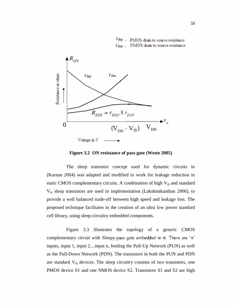
Figure 3.1 Pass gate (transmission gate) logic
The Figure 3.2 plots ON resistance (RON) of pass gate as input
voltage is swept from Gnd to VDD, assuming the output voltage closely
follows. The effective ON resistance is a parallel combination of two
resistances and is relatively constant across full range of input voltages.
However the OFF resistance is very high and it is in the range of several mega
ohms.
58
Figure 3.2 ON resistance of pass gate (Weste 2005)
The sleep transistor concept used for dynamic circuits in
(Kursun 2004) was adapted and modified to work for leakage reduction in
static CMOS complementary circuits. A combination of high Vth and standard
Vth sleep transistors are used in implementation (Lakshmikanthan 2006), to
provide a well balanced trade-off between high speed and leakage loss. The
proposed technique facilitates in the creation of an ultra low power standard
cell library, using sleep-circuitry embedded components.
Figure 3.3 illustrates the topology of a generic CMOS
complementary circuit with Sleepy-
inputs, input 1, input 2....input n, feeding the Pull-Up Network (PUN) as well
as the Pull-Down Network (PDN). The transistors in both the PUN and PDN
are standard Vth devices. The sleep circuitry consists of two transistors, one
PMOS device S1 and one NMOS device S2. Transistors S1 and S2 are high
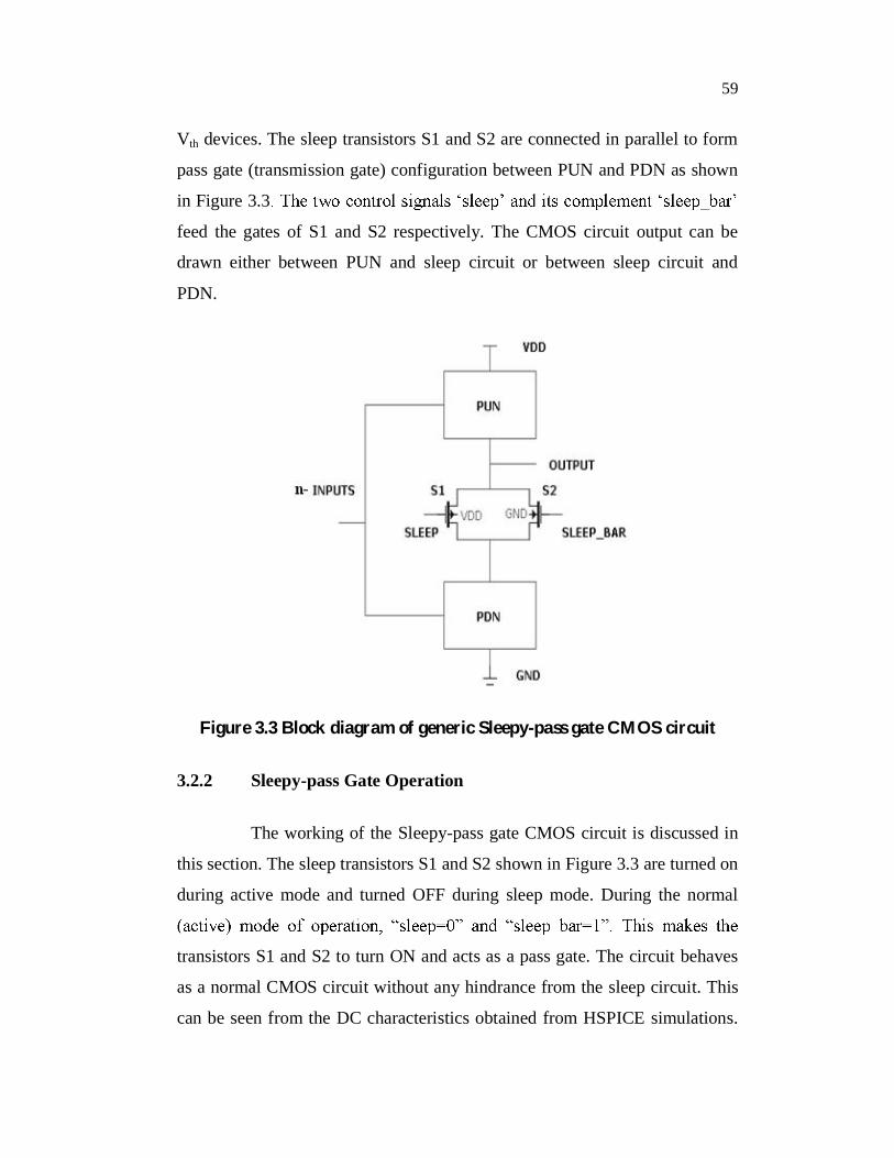
59
Vth devices. The sleep transistors S1 and S2 are connected in parallel to form
pass gate (transmission gate) configuration between PUN and PDN as shown
in Figure 3.3
feed the gates of S1 and S2 respectively. The CMOS circuit output can be
drawn either between PUN and sleep circuit or between sleep circuit and
PDN.
Figure 3.3 Block diagram of generic Sleepy-pass gate CMOS circuit
3.2.2 Sleepy-pass Gate Operation
The working of the Sleepy-pass gate CMOS circuit is discussed in
this section. The sleep transistors S1 and S2 shown in Figure 3.3 are turned on
during active mode and turned OFF during sleep mode. During the normal
transistors S1 and S2 to turn ON and acts as a pass gate. The circuit behaves
as a normal CMOS circuit without any hindrance from the sleep circuit. This
can be seen from the DC characteristics obtained from HSPICE simulations.

60
Figure 3.4 shows a two input NAND gate with Sleepy-pass gate embedded.
Figure 3.5 shows the DC characteristics of the NAND gate with the proposed
method (the input A is fixed at 1 V and B is varied from 0 to 1 V).
Figure 3.4 Two input NAND gate with Sleepy-pass gate structure
Figure 3.5 DC characteristic of a two input NAND with Sleepy-pass gate

61
The ON resistance of the pass gate will be constant and lesser than
its OFF resistance, allowing conduction between PUN and PDN. Even though
the ON resistance of pass gate is not as high as its OFF state resistance, it
increases the resistance of VDD to ground path, controlling the flow of leakage
currents, resulting in leakage power reduction in active mode. In standby
S2 to turn OFF forcing a high-impedance condition between PUN and PDN
nodes.
Thus, the introduction of Sleepy- pass gate increases the resistance
of the path from VDD to ground during standby mode of operation resulting in
reduction of leakage current. The leakage reduction of the Sleepy-pass gate
structure occurs in two ways. First, leakage power is suppressed by high Vth
transistors, which are applied to the sleep transistors and the transistors
parallel to the sleep transistors. Second, increases the resistance of the path
from VDD to ground during standby mode, which also suppresses leakage
power consumption.
By combining these two effects, the Sleepy-pass gate structure
achieves ultra low leakage power consumption during sleep mode while
retaining exact logic state. Figure 3.6 shows the input-output curves of the
NAND gate with proposed method simulated for 100-nm technology at 1V
supply voltage. It can be observed from the curves that the proposed NAND
gate produces exact output logic levels. For any given process technology,
the standard Vth transistors are unit-sized devices (the smallest width to length
W/L ratio as defined by the technology). However, the high Vth transistors S1
and S2 needs to be sized appropriately for the Sleepy-pass gate embedded
CMOS cells to have a propagation delay comparable to that of the standard
cells.

62
Figure 3.6 Input - output waveforms of a two input NAND with proposed method
There is a nominal increase in both area and propagation delay of
the Sleepy-pass gate embedded circuit, when compared to the standard
CMOS circuits. This overhead of Sleepy-pass gate embedded cells is traded-
off against enormous power savings, when compared to the standard CMOS
cells. In addition to that, output logic state is not lost when the circuit enters
from mode to sleep mode and vice-versa. This seems attractive in comparison
with some of the existing ways to use far lower VDD values and additional
transistors to maintain logic state. Flautner (2002) also propose that some
reduced VDD values sufficient to maintain the logic state.
As an alternative option, the Sleepy-pass gate could be used
between the supply voltage VDD and PUN and/or PDN and ground during
active mode of operation. This will create virtual supply and/or ground rails.
During standby mode, all sleep transistors are off, thus the actual power and
63
ground path are broken and the circuit experiences lower voltage. A very high
resistance path is established between VDD and ground due to the parallel
combination of the off resistance of sleep transistors and the leakage current
flowing through the circuit reduces significantly and hence lowest power
dissipation.
3.3 EVALUATION OF SLEEPY-PASS GATE TECHNIQUE
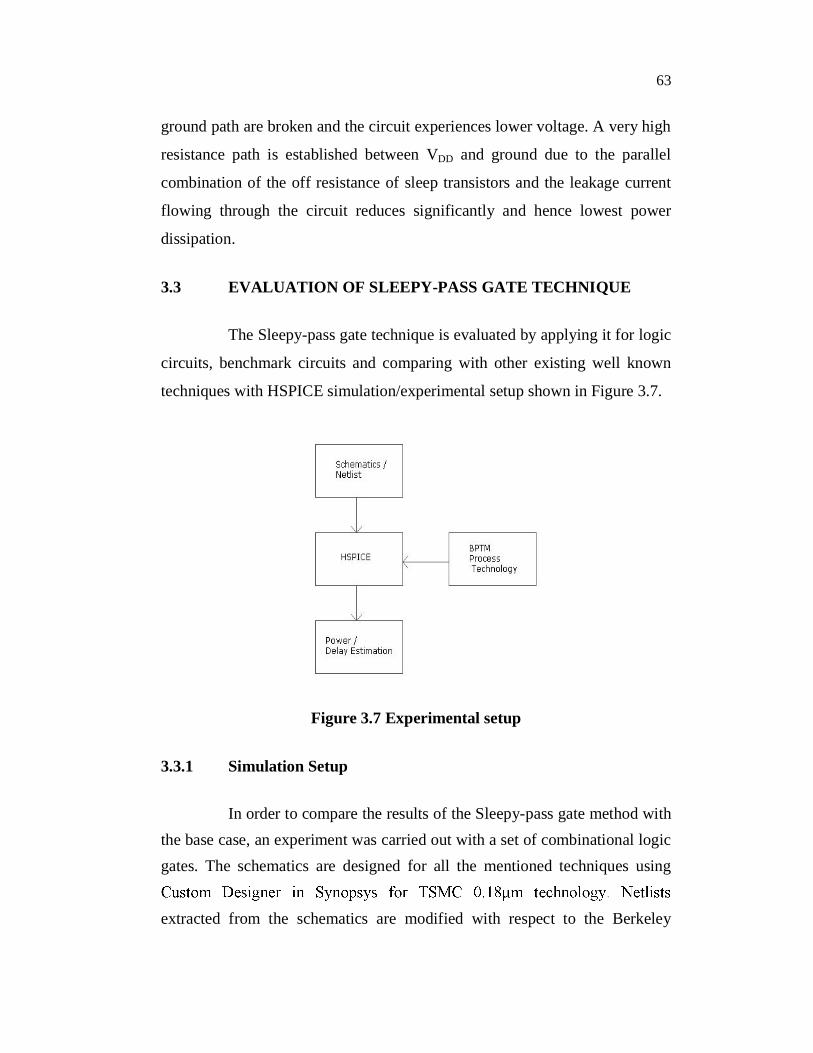
The Sleepy-pass gate technique is evaluated by applying it for logic
circuits, benchmark circuits and comparing with other existing well known
techniques with HSPICE simulation/experimental setup shown in Figure 3.7.
Figure 3.7 Experimental setup
3.3.1 Simulation Setup
In order to compare the results of the Sleepy-pass gate method with the base case, an experiment was carried out with a set of combinational logic gates. The schematics are designed for all the mentioned techniques using
extracted from the schematics are modified with respect to the Berkeley

64
Predictive Technology Models. The modified netlists are simulated using Synopsys HSPICE for power and delay measurements.
3.3.2 Applying Sleepy-pass Gate for Logic Circuits
Various circuit applications of the Sleepy-pass gate technique are explored. The generic logic circuits including inverter, NAND2, NOR2, AND2, OR2, multiplexer and full adder gates are implemented using state empirical saving as well as state-destructive low leakage techniques for evaluation. Detailed experimental methodology is explained.
All circuits were simulated at a temperature of 25°C. Standard combinational CMOS library cells, such as NOR2, NAND2, OR2, AND2, XOR2, XNOR2 and MUX2x1, were implemented (Sahni 2006) using
and modified accordingly for respective process technologies. Transistor sizes in all these circuits were fixed, and taken as PMOS width WP = 2 NMOS width WN = 1L=100nm. A supply voltage (VDD) of 1V was used and transient analysis performed on all 7 cells listed above, using HSPICE. The output load for each of the 7 cells was a capacitor of 1pF.
3.3.2.1 Simulation results for logic gates
The total area of each standard cell in CMOS base case and proposed method is listed in Table 3.1. There is a slight increase in area for the proposed technique compared with base case due to additional transistors. Figure 3.8 and Figure 3.9 shows the layout for basic NAND and NOR gates for example. The propagation delay of each cell was measured for the purpose of comparing between base case and Sleepy-pass gate embedded cells. Next, the circuits were simulated at a temperature of 25oC and their leakage power measured. All possible input combinations were applied and leakage power loss measured in every case. Column 2 of Table 3.2 lists the average leakage power loss for each standard CMOS cell.

65
Figure 3.8 Two input CMOS NAND gate layout
Next, the Sleepy-pass gate circuitry was introduced for all
7 standard CMOS cells. The sleep transistors S1 and S2 are unit sized as
WS1 = WS2
100nm process technology. For each cell, transient analysis was performed in
the normal mode of operatio _
propagation delays were calculated and compared to the standard circuit
values as shown in Figure 3.10.
Figure 3.9 Two input NOR gate layout

66
Figure 3.10 Propagation delay comparison @100nm with VDD =1 V
The high Vth sleep transistor(s) were sized such that the propagation delay of the Sleepy-pass gate cell was comparable to that of the standard cell. The Figure 3.10 shows that there is an increased delay for proposed technique compared to base case due to additional transistors. Finally, the Sleepy-pass gate embedded cell was simulated in the sleep (standby) mode of operation
_3 of Table 3.2 lists the leakage power loss for all the Sleepy-pass gate embedded standard cells. Column 4 of Table 3.2 gives folds of leakage power savings on using the Sleepy-pass gate on combinational cells.
Table 3.1 Area measurements for combinational cells @ 100nm process
Area (µm2) CMOS Gate Base Case Sleepy-pass Gate
2 input NAND 36.290 40.188 2 input NOR 42.835 46.456 2 input XOR 213.430 217.460 2 input AND 50.246 64.843 2 input OR 61.278 78.129 2 input MUX 202.109 218.213 1-bit Full Adder 623.765 651.340

67
Table 3.2 Leakage power for combinational cells @ 100nm process
Average Leakage Power (W) with VDD = 1 Volt
CMOS Gate Base Case Sleepy-pass Gate Leakage Savings
2 input NAND 5.1700 E-08 2.8710 E-10 180 X
2 input NOR 5.4830 E-08 3.1959 E-10 170 X
2 input XOR 12.3677 E-08 8.2780 E-10 148 X
2 input AND 6.3950 E-08 4.8477 E-10 140 X
2 input OR 6.9464 E-08 5.2567 E-10 131 X
2 input MUX 6.3748 E-07 7.3758 E-09 85 X
1-bit Full Adder 8.9000 E-07 3.5600 E-09 249 X
3.3.2.2 Increase in dynamic power dissipation
The main emphasis till now has been on the standby (sleep) mode leakage power loss of the Sleepy-pass gate embedded cells. The dynamic power loss of these circuits has not been explored as yet. The dynamic power dissipation depends mainly on transient switching activity and frequency of operation, as well as on the square of the supply voltage.
In this section, the effect of the additional sleep circuitry components on dynamic power dissipation of standard cells is studied. The combinational standard library cells were used, and their dynamic power measured. Table 3.3 gives the dynamic power dissipation comparison between standard CMOS cells (base case) and Sleepy-pass gate embedded cells. Column 2 of Table 3.3 gives the dynamic power loss of standard CMOS cells. Column 3 of Table 3.3 lists the dynamic power dissipation of the Sleepy-pass gate embedded cells. Analysis of results in Table 3.3 shows that the dynamic power penalty (increase) of the Sleepy-pass gate embedded, when compared to that of standard cells is due to the additional transistors introduced and the consequent capacitive increase in the sleep-embedded circuits.

68
Table 3.3 Dynamic power for combinational cells @100nm process
Dynamic Power ( E -06 W) @ VDD=1V
Combinational Cells Base Case Sleepy-pass Gate
2 input NAND 7.7644 8.1902
2 input NOR 7.8190 8.2811
2 input XOR 12.0038 13.7445
2 input AND 9.0923 11.7016
2 input OR 8.9202 11.7391
2 input MUX 11.4912 12.0230
1-bit Full Adder 73.0032 90.1091
The literature detailing various methods to reduce dynamic power
has been analyzed and can be summarized as follows:
Clock and Signal Gating
This is the simplest and most straight forward method to reduce
transient switching activity of the highly active nodes in a circuit. Control
signal gating techniques, like those presented by Kapadia (1999), target
reduction in switching power.
Operand Isolation Techniques
The input sharing problem is typically the cause of unnecessary
switching activity in modules where there should be none. Consider a simple
Arithmetic and Logic Unit (ALU) designed for 4 operations (add, subtract,
multiply and shift), all sharing 2 input signals -
shifter units are simultaneously active along with the subtractor, thereby

69
wasting power. Operand isolation techniques, like using multiplexers or using
multiple registers to drive different modules, solve the input-sharing problem.
However, this increases the area and the delay, and adds other overheads.
Transistor Re-ordering Techniques
Hossain (1996) used a probability based transistor re-ordering
technique to reduce dynamic power dissipation in CMOS circuits.
Circuits Comprised of Independent Voltage Islands
Lackey (2002) presented a comprehensive background on methods
used to design voltage islands. They present various voltage island scenarios,
a system architecture and chip implementation methodology, which are used
to reduce active and static power consumption in SOC designs. The design
implications of voltage islands are also evaluated.
Carballo (2003) proposed a semi-custom voltage island approach to
build high-speed serial links. Their approach is a mixture of selective custom
design and the transparent use of multiple supplies to reduce power. The
digital circuitry on the chip runs at a low supply voltage, while the analog
circuitry runs at a higher voltage level. An on-chip regulator converts low to
high voltage, and vice-versa. MTCMOS transistors are used in the custom
design process.
Hillman (2005) focused on minimizing the operating voltage to
reduce dynamic power. The library of components created was characterized
for different voltages. Next, the whole SOC design was built with various
components from this library, using voltage level-shifting circuits and voltage
isolation cells.

70
Hung (2005) presented a voltage island partitioning and floor
planning algorithm for architecting SOC designs. Their work explores the
thermal impact of voltage islands. A hybrid optimization approach consisting
of a genetic algorithm based (GA-based) voltage island partitioning algorithm
and a simulated annealing based (SA-based) floor-planning algorithm, is
presented.
3.3.3 Applying Sleepy-pass Gate for Benchmark Circuits
The ISCAS'85 benchmark circuits are ten combinational networks
provided to authors at the 1985 International Symposium on Circuits and
Systems. They subsequently have been used by many researchers as a basis
for comparing results in several areas of digital design, including test
generation, timing analysis, and technology mapping.
Experiments were conducted on a variety of combinational multi
implemented using various deep
submicron process technologies. The HSPICE simulator, in conjunction with
the BPTM deep submicron technology, was used to simulate circuits and to
estimate leakage power dissipation.
All circuits (unless specified otherwise) were simulated at a
temperature of 25oC. The Berkeley Predictive Technology Models (BPTM)
contained process parameters and values only for standard Vth PMOS and
NMOS transistors. No models are available for high Vth transistors. Except
the Sleepy-pass gate transistors, the width for all other transistors are taken as
Wp = 3 µm and Wn=1µm for PMOS and NMOS respectively.
Experiments using some proprietary technology models obtained
directly from foundries showed an interesting trend in the threshold voltage

71
value of high Vth transistors. For a variety of deep-submicron technologies,
we observed that the threshold voltage value of a high Vth PMOS or a high Vth
NMOS transistor was 25%-35% more than that of a standard Vth transistor.
Hence, models for high Vth PMOS and NMOS transistors were incorporated
into BPTM with threshold voltage values 25% more than that of standard Vth
transistors. DC simulations were run using HSPICE to ensure that the
threshold values of these high Vth transistors were only 25% more than those
of standard Vth transistors.
Table 3.4 and Table 3.5 lists the supply and threshold voltage
values for various BPTM models for PMOS and NMOS transistors
respectively. The first columns in Tables 3.4 and 3.5 list the technology
feature size. The supply voltage used for each feature size is listed in Column
2 of both Table 3.4 and Table 3.5. Column 3 of Table 3.4 gives the threshold
voltage of a standard PMOS transistor, while Column 3 of Table 3.5 gives the
threshold voltage of a standard NMOS transistor. The threshold voltage of a
high Vth PMOS transistor is listed in Column 4 of Table 3.4 and the threshold
voltage of a high Vth NMOS transistor is listed in Column 4 of Table 3.5.
Table 3.4 PMOS threshold voltage for BPTM models
BPTM Process VDD PMOS Standard Vth PMOS High Vth
180nm 1.8V -0.42V -0.35V
130nm 1.3V -0.35V -0.32V
100nm 1.0V -0.30V -0.28V
70nm 0.85V -0.22V -0.18V

72
Table 3.5 NMOS threshold voltage for BPTM models
BPTM Process VDD NMOS Standard Vth NMOS High Vth 180nm 1.8V 0.41V 0.55V
130nm 1.3V 0.33V 0.38V
100nm 1.0V 0.26V 0.34V
70nm 0.85V 0.21V 0.39V
3.3.3.1 85 leakage values
Ten experimental
characteristics given in Table 3.6 with Sleepy-pass gate embedded. They were
sized appropriately for 4 different deep-submicron technologies - 180 nm,
130 nm, 100nm and 70 nm. The PMOS and NMOS are sized with width to
length ratio as W/L = 6 and W/L = 3 respectively except for the Sleepy-pass
gates.
Table 3.6 ISCAS '85 benchmark circuit characteristics
Circuit Name Circuit Function Total Gates Input
Lines Output Lines
C432 Priority Decoder 160(18 XOR) 36 7
C499 32-Bit Single-Error-Correcting Circuit 202(104 XOR) 41 32
C880 ALU and Control 383 60 26
C1355 32-Bit Single-Error-Correcting Circuit 546 41 32
C1908 16-bit error detector/ corrector 880 33 25
C2670 ALU and Control 1193 233 140 C3540 ALU and Control 1669 50 22 C5315 ALU and Selector 2307 178 123 C6288 16-bit Multiplier 2406 32 32 C7552 ALU and Control 3512 207 108
73
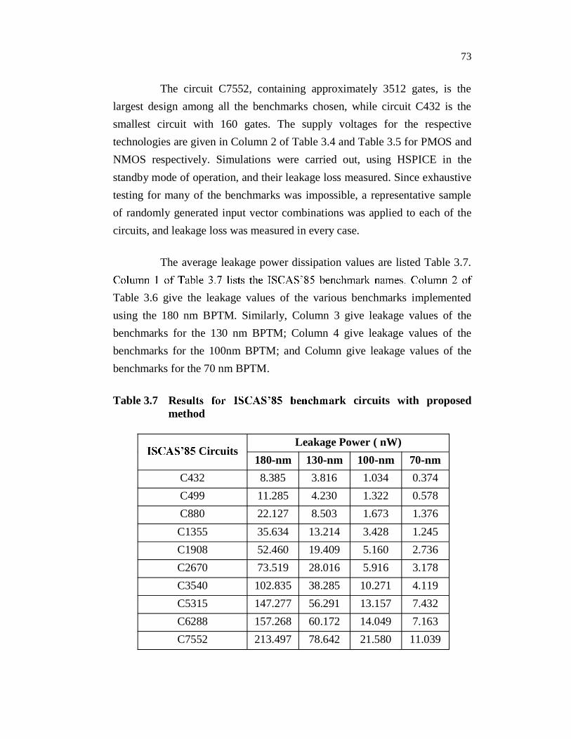
The circuit C7552, containing approximately 3512 gates, is the largest design among all the benchmarks chosen, while circuit C432 is the smallest circuit with 160 gates. The supply voltages for the respective technologies are given in Column 2 of Table 3.4 and Table 3.5 for PMOS and NMOS respectively. Simulations were carried out, using HSPICE in the standby mode of operation, and their leakage loss measured. Since exhaustive testing for many of the benchmarks was impossible, a representative sample of randomly generated input vector combinations was applied to each of the circuits, and leakage loss was measured in every case.
The average leakage power dissipation values are listed Table 3.7.
Table 3.6 give the leakage values of the various benchmarks implemented using the 180 nm BPTM. Similarly, Column 3 give leakage values of the benchmarks for the 130 nm BPTM; Column 4 give leakage values of the benchmarks for the 100nm BPTM; and Column give leakage values of the benchmarks for the 70 nm BPTM.
Table 3.7 R rk circuits with proposed method
Circuits Leakage Power ( nW)
180-nm 130-nm 100-nm 70-nm C432 8.385 3.816 1.034 0.374 C499 11.285 4.230 1.322 0.578 C880 22.127 8.503 1.673 1.376 C1355 35.634 13.214 3.428 1.245 C1908 52.460 19.409 5.160 2.736 C2670 73.519 28.016 5.916 3.178 C3540 102.835 38.285 10.271 4.119 C5315 147.277 56.291 13.157 7.432 C6288 157.268 60.172 14.049 7.163 C7552 213.497 78.642 21.580 11.039

74
3.3.4 Prior Low Leakage Techniques Considered for Comparison
Purposes
The Sleepy-pass gate technique is compared to a conventional
CMOS approach, which is the base case, and four other well-known previous
approaches, i.e., the forced stack, sleep, zigzag and LECTOR techniques. The
four bit adder circuit is chosen for implementation and comparison.
3.3.4.1 Four bit adder
By use of the one bit full adder shown in Figure 3.11, four bit adder
shown in Figure 3.12 is implemented. A full adder is an example of a typical
complex CMOS gate. In Figure 3.11, a and b are two inputs and c is a carry
input. Carry and Sum are outputs. The transistor sizing of the full adder is
noted in Figure 3.11.
Figure 3.11 One bit full adder

75
Figure 3.12 Inputs of four bit adder
3.3.4.2 Base case
CMOS technique has shown in Figure 3.13 and described in a classic
textbook by Weste (2005). Figure 3.13 shows a pull-up network and a pull-
down network using as few transistors as possible to implement the Boolean
logic function desired. The base case of a four bit adder is sized as explained
in Section 3.3.4.1.
Figure 3.13 Base case
76
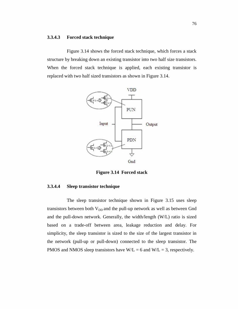
3.3.4.3 Forced stack technique
Figure 3.14 shows the forced stack technique, which forces a stack
structure by breaking down an existing transistor into two half size transistors.
When the forced stack technique is applied, each existing transistor is
replaced with two half sized transistors as shown in Figure 3.14.
Figure 3.14 Forced stack
3.3.4.4 Sleep transistor technique
The sleep transistor technique shown in Figure 3.15 uses sleep
transistors between both VDD and the pull-up network as well as between Gnd
and the pull-down network. Generally, the width/length (W/L) ratio is sized
based on a trade-off between area, leakage reduction and delay. For
simplicity, the sleep transistor is sized to the size of the largest transistor in
the network (pull-up or pull-down) connected to the sleep transistor. The
PMOS and NMOS sleep transistors have W/L = 6 and W/L = 3, respectively.

77
Figure 3.15 Sleep technique
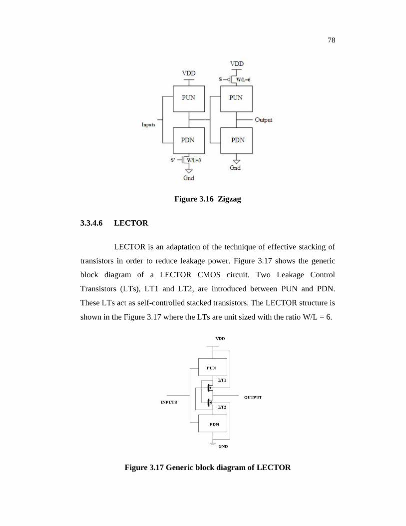
3.3.4.5 Zigzag
The zigzag technique in Figure 3.16 uses one sleep transistor in
each logic stage either in the pull-up or pull-down network according a
particular input pattern. In this thesis, an input vector is used that can achieve
the lowest possible leakage power consumption. Then, either assign a sleep
transistor to the pull- it is assigned to
the pull- . For Figure 3.16, it is assumed that the
minimum leakage inputs are asserted.
Therefore, a pull-down sleep transistor is assigned for the first stage
and a pull-up sleep transistor for the second stage. Similar to the sleep
transistor technique, the size of the sleep transistors are sized to that of the
largest transistor in the network (pull-up or pull-down) connected to the sleep
transistor. The PMOS and NMOS sleep transistors have W/L = 6 and
W/L = 3, respectively.
78
Figure 3.16 Zigzag
3.3.4.6 LECTOR
LECTOR is an adaptation of the technique of effective stacking of
transistors in order to reduce leakage power. Figure 3.17 shows the generic
block diagram of a LECTOR CMOS circuit. Two Leakage Control
Transistors (LTs), LT1 and LT2, are introduced between PUN and PDN.
These LTs act as self-controlled stacked transistors. The LECTOR structure is
shown in the Figure 3.17 where the LTs are unit sized with the ratio W/L = 6.
Figure 3.17 Generic block diagram of LECTOR

79
3.3.5 Experiments on Sleepy-pass Gate
3.3.5.1 Delay
The worst case propagation delay of each benchmark is measured.
Input vectors and input and output triggers are chosen to measure delay across
trigger input edge reaching 50% of the supply voltage value and the circuit
output edge reaching 50% of the supply voltage value. Input waveforms have
a 4ns period (i.e., a 250 MHz rate) and rise and fall times of 100ps.
3.3.5.2 Active power
Active power is measured by asserting semi-random input vectors
and calculating the average power dissipation during this time. Input vectors
are chosen so that a large number of possible input combinations are included
in the set. The average power dissipation reported by HSPICE is taken as the
estimate of active power consumption.
This active power includes dynamic power as well as static power
during the time measured. However, static power consumption is subtracted
to calculate pure dynamic power consumption. All sleep transistors are turned
on when active power is measured for the sleep, zigzag and Sleepy-pass gate
techniques.
For the four bit adder, input vectors covering every possible input
are asserted. The waveform in Figure 3.18 shows input vectors asserted for
each one bit adder, where the input vector changes in every 4ns. The same
signal timing is used while scaling technology from 0.18
signal timing is not customized )

80
because in this way the effect of technology scaling on a fixed clock can be
observed. However, it is known that reducing cycle time along with
technology feature size is possible and may reveal additional insights and
tradeoffs.
3.3.5.3 Static power
HSPICE is also used to measure static power consumption. Since
static power varies according to input state, either a full combination of input
vectors or subset of possible input combinations is considered. When static
power is measured, first an input vector is asserted and power consumption is
measured after signals become stable (e.g., after 30ns). Each measured static
power consumption over 30ns is averaged to derive static power consumption
of each circuit.
Figure 3.18 One bit adder input-output signals for dynamic power measurement
For the four bit adder, all possible input vectors of a full adder are
considered for leakage power measurement. The sleep transistors of the sleep,

81
zigzag and Sleepy-pass gate techniques are turned OFF during sleep mode in
which the leakage power dissipation is measured.
3.3.5.4 Area
particular design style (e.g., base case) is measured using layout. For a four
bit adder, an actual full layout of adder is directly measured and estimated
scaling the area of each benchmark layout for each particular design style
Around 10% area overhead is added in order to consider non-linear 2
m process, the area for 2 x (0.130/0.180) x 1.1 is estimated.
To estimate
technologies, extra area needed to wire gates is not taken into account but the
absence of a wiring penalty equally affects all techniques considered (i.e, base
case, sleep, forced stack, zigzag, LECTOR and Sleepy-pass gate). Figure 3.19
shows the layout of a full adder.

82
Figure 3.19 Layout of full adder
83
3.3.6 Comparative Results
First the Sleepy-pass gate is compared to the base case and
LECTOR techniques (self triggered sleep circuitry) in terms of leakage power
and delay using a two input NAND gate at temperature 25oC. Secondly with
well-known techniques, i.e., sleep, zigzag, and forced stack, in terms of active
power, leakage power, area and delay using four bit full adder circuit
explained in Section 3.3.4.1.
3.3.6.1 Results of two input NAND gate
Tables 3.8, 3.9 and 3.10 gives the leakage power, savings and delay
penalty comparison for the base case, LECTOR and Sleepy-pass gate
embedded NAND gates respectively. For a fair comparison, the supply
voltage was set to 1V for the 100nm. In Table 3.8 the values reported in rows
3 list the leakage power values for a base case NAND gate, using BPTM
100nm. In Table 3.8 row 4 list the leakage values for the LECTOR NAND
gate, using BPTM 100nm. Table 3.8 row 5 gives the leakage (in standby
mode) values for the Sleepy-pass gate embedded NAND gate, using BPTM
100nm. Column 2 to column 5 of Table 3.8 indicates the corresponding input
vectors applied to the gates. Analysis of the results in Table 3.8 shows that the
leakage power is dependent on input vector applied to the circuits.
(Abdollahi 2004).
Column 2 and column 3 of Table 3.9 presents the average leakage
power and leakage savings obtained for base case, LECTOR and Sleepy-pass
gate NAND gates. It shows that the Sleepy-pass gate technique has the least
leakage power dissipation and largest leakage savings of 180% when
compared to the conventional CMOS NAND gate. Column 2 and column 3 of
Table 3.10 gives the delay obtained by introducing the additional transistors
and the corresponding delay penalty respectively. It shows that the
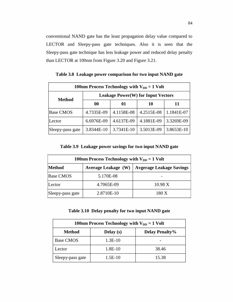
84
conventional NAND gate has the least propagation delay value compared to
LECTOR and Sleepy-pass gate techniques. Also it is seen that the
Sleepy-pass gate technique has less leakage power and reduced delay penalty
than LECTOR at 100nm from Figure 3.20 and Figure 3.21.
Table 3.8 Leakage power comparison for two input NAND gate
100nm Process Technology with VDD = 1 Volt
Method Leakage Power(W) for Input Vectors
00 01 10 11
Base CMOS 4.7335E-09 4.1158E-08 4.2515E-08 1.1841E-07
Lector 6.6976E-09 4.6137E-09 4.1881E-09 3.3269E-09
Sleepy-pass gate 3.8344E-10 3.7341E-10 3.5013E-09 3.8653E-10
Table 3.9 Leakage power savings for two input NAND gate
100nm Process Technology with VDD = 1 Volt
Method Average Leakage (W) Avgerage Leakage Savings
Base CMOS 5.170E-08 -
Lector 4.7065E-09 10.98 X
Sleepy-pass gate 2.8710E-10 180 X
Table 3.10 Delay penalty for two input NAND gate
100nm Process Technology with VDD = 1 Volt
Method Delay (s) Delay Penalty%
Base CMOS 1.3E-10 -
Lector 1.8E-10 38.46
Sleepy-pass gate 1.5E-10 15.38

85
Figure 3.20 Average leakage power for two input NAND gate
Figure 3.21 Propagation delay for two input NAND gate
3.3.6.2 Results of four bit full adder
The impact of technology scaling is explored from the results of a
four bit full adder in terms of static power, propagation delay, dynamic power

86
and area as tabulated in Table 3.11 to Table 3.14. Table 3.11 gives the static
power dissipation for 180nm, 130nm, 100nm and 70nm process technologies.
Table 3.11 shows that the Sleepy-pass gate achieves large leakage reduction
over the base case and the other compared leakage reduction techniques.
From Figures 3.22, 3.23, 3.24 and 3.25 it is observed that static power
increases as technology feature size shrinks.
Table 3.12 gives the propagation delay of a four bit full adder
implemented in base case as well as other leakage reduction techniques
including Sleepy-pass gate at 180nm, 130nm, 100nm and 70nm process
technologies. From Figure 3.26 it is observed that propagation delay
decreases as technology feature size shrinks. Compared to the base case,
Sleepy-pass gate has increasing delay and smaller when compared with
LECTOR technique.
Table 3.11 Static power dissipation for various process technologies
Static Power (W) of Four Bit Full Adder
4-bit adder 180nm 130nm 100nm 70nm
Base case 9.39E-10 9.34E-09 9.57E-08 9.31E-07
Forced stack 9.47E-11 8.36E-10 8.29E-09 7.28E-08
Sleep 7.28E-10 5.20E-09 6.40E-08 6.27E-07
Zigzag 4.28E-10 1.82E-09 4.09E-08 4.89E-08
LECTOR 8.11E-11 9.31E-11 9.87E-09 1.62E-08
Sleepy-pass gate 6.13E-11 1.52E-11 7.21E-09 2.84E-09
87
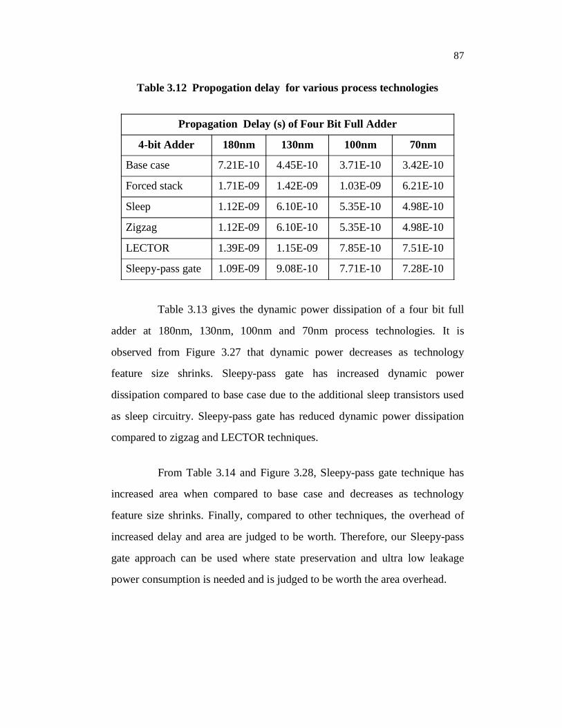
Table 3.12 Propogation delay for various process technologies
Propagation Delay (s) of Four Bit Full Adder
4-bit Adder 180nm 130nm 100nm 70nm
Base case 7.21E-10 4.45E-10 3.71E-10 3.42E-10
Forced stack 1.71E-09 1.42E-09 1.03E-09 6.21E-10
Sleep 1.12E-09 6.10E-10 5.35E-10 4.98E-10
Zigzag 1.12E-09 6.10E-10 5.35E-10 4.98E-10
LECTOR 1.39E-09 1.15E-09 7.85E-10 7.51E-10
Sleepy-pass gate 1.09E-09 9.08E-10 7.71E-10 7.28E-10
Table 3.13 gives the dynamic power dissipation of a four bit full
adder at 180nm, 130nm, 100nm and 70nm process technologies. It is
observed from Figure 3.27 that dynamic power decreases as technology
feature size shrinks. Sleepy-pass gate has increased dynamic power
dissipation compared to base case due to the additional sleep transistors used
as sleep circuitry. Sleepy-pass gate has reduced dynamic power dissipation
compared to zigzag and LECTOR techniques.
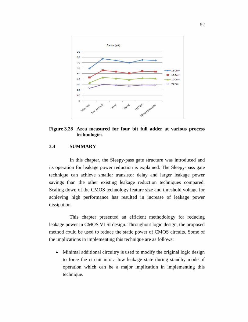
From Table 3.14 and Figure 3.28, Sleepy-pass gate technique has
increased area when compared to base case and decreases as technology
feature size shrinks. Finally, compared to other techniques, the overhead of
increased delay and area are judged to be worth. Therefore, our Sleepy-pass
gate approach can be used where state preservation and ultra low leakage
power consumption is needed and is judged to be worth the area overhead.

88
Table 3.13 Dynamic power dissipation for various process technologies
Dynamic Power Dissipation (W) of Four Bit Full Adder
4-bit Adder 180nm 130nm 100nm 70nm
Base case 4.81E-04 1.20E-04 3.82E-05 1.86E-05
Forced stack 5.70E-04 1.42E-04 4.38E-05 2.31E-05
Sleep 5.53E-04 1.37E-04 4.25E-05 2.21E-05
Zigzag 6.54E-04 1.67E-04 5.18E-05 2.83E-05
LECTOR 5.74E-04 1.43E-04 4.42E-05 2.93E-05
Sleepy-pass gate 5.66E-04 1.41E-04 4.35E-05 2.82E-05
Table 3.14 Area measured for various process technologies
Area (µm2)of Four Bit Full Adder
4-bit Adder 180nm 130nm 100nm 70nm
Base case 59.54 43.00 33.07 23.15
Forced stack 77.35 55.86 42.97 30.08
Sleep 74.15 53.55 41.18 28.8
Zigzag 69.89 50.47 38.83 27.18
LECTOR 75.13 54.26 41.73 29.2
Sleepy-pass gate 74.25 53.62 41.25 28.8

89
Figure 3.22 Static power for four bit full adder at 180nm
Figure 3.23 Static power for four bit full adder at 130nm

90
Figure 3.24 Static power for four bit full adder at 100nm
Figure 3.25 Static power for four bit full adder at 70nm

91
Figure 3.26 Propagation delay for four bit full adder at various process technologies
Figure 3.27 Dynamic power dissipation for four bit full adder at various process technologies
92
Figure 3.28 Area measured for four bit full adder at various process technologies
3.4 SUMMARY
In this chapter, the Sleepy-pass gate structure was introduced and its operation for leakage power reduction is explained. The Sleepy-pass gate technique can achieve smaller transistor delay and larger leakage power savings than the other existing leakage reduction techniques compared. Scaling down of the CMOS technology feature size and threshold voltage for achieving high performance has resulted in increase of leakage power dissipation.
This chapter presented an efficient methodology for reducing leakage power in CMOS VLSI design. Throughout logic design, the proposed method could be used to reduce the static power of CMOS circuits. Some of the implications in implementing this technique are as follows:
Minimal additional circuitry is used to modify the original logic design to force the circuit into a low leakage state during standby mode of operation which can be a major implication in implementing this technique.
93
This technique requires a controller / power management system to automatically generate sleep signals during standby mode and also to activate it when necessary.
There is a tradeoff between area, delay and power by utilizing this technique for power savings. DT-LECTOR is proposed in next chapter which could be used in applications that demand high speed and where sleep signal control circuitry is not available.