Embed Size (px)
Citation preview

75
CHAPTER 3
FPGA IMPLEMENTATION OF DS-CDMA
COMMUNICATION SYSTEM
3.1 CDMA COMMUNICATION SYSTEM
A cellular communication system in which the bandwidth is shared
by all subscribers, each with a different spreading code, is called Code
Division Multiple Access (CDMA) system. In other words, a large number of
users share a common pool of radio channels and any user can get access to
some channel. Different types of cellular systems employ various schemes to
achieve this multiple access. The traditional analog cellular systems use
Frequency Division Multiple Access (FDMA) as shown in Figure 3.1 and
Time Division Multiple Access (TDMA) as shown in Figure 3.2 and. TDMA
and FDMA systems divide each carrier into time slot and frequency slot
(channels) and then only one subscriber at a time is assigned each time slot
and channel respectively in Rappoport (2010). On the other hand, Code
Division Multiple Access (CDMA) as shown in Figure 3.3, it uses unique
digital codes rather than separate RF frequencies or Channels to differentiate
subscribers. The codes are shared by both base station and Mobile station.
These - other
research work in the field of Spectral Division Multiple Access (SDMA) or
Space Division Multiple Access (SPDM) is in progress. These are more
efficient and advanced research areas.

76
Figure 3.1 Frequency division multiple access
Figure 3.2 Time division multiple access
Use
r 1
Use
r 2
Use
r n
. . .
Freq
uenc
y
Time
User n
User 2
User 1
.
. .
Freq
uenc
y
Time

77
Figure 3.3 Code division multiple access
Originally the CDMA was used to jam the communications or to
hide the fact that communication is even taking place. This is achieved by
spreading the information contained in a particular signal over a much wider
bandwidth. In recent times, CDMA has gained widespread international
acceptance by cellular radio system operators since it is considered as an
advancement and breakthrough in communication technology that has
increased both system capacity and service quality.
A CDMA system typically begins with a standard rate of 9. 60 kbps
and then it is spread to a typical transmitting rate of 1.23 Mbps.
The spreading of data using DS-SS technique is illustrated in
Figure 3.4. Spreading is done by adding a digital code, normally called
Pseudo-Noise (PN) sequence, to the data bits associated with users in a cell.
At the receiver, the pseudo codes are removed from received signals and a
call is received at the rate of 9.60 kbps. Due to wide bandwidth of spread
spectrum signal, the possibility of any interference, detection or jamming is
greatly reduced. The CDMA, therefore, enhance the intensity of privacy and
defense. Spreading is the key to ever-increasing the defense intensity in

78
communication systems, while the code of signal can be spread in excess of
the whole carrier, is to be very firm to detect or intercept in Min Shi
Figure 3.4 Spreading of data using DS-SS technique
The CDMA systems have merits and demerits as usual with any
other system. These include higher capacity by a factor of 8 to 10 compared
to other systems, improved call quality with a better and more consistent
performances, simple system planning through the use of the same frequency
in every sector, enhanced privacy, coverage area, talk time duration and
bandwidth utility. CDMA system, similar to many other systems, has
demerits as well. These may consist of that there is a necessary for very well-
organized power control to ensure homogeneous signal strength at the
receiving antenna. Failure to this may result in one user swamping each and
every part of others. Channel contamination may take place when similarly
dominant signals from various base stations are present at receiving antenna
in Magaa et al (2007). Hurdles and multiple reflections caused by tall
buildings and hills etc may decrease the performance.
m(t)
c(t)
ms(t)

79
3.1.1 Proposed Architecture of DS-CDMA Communication Transceiver
A typical block diagram of CDMA transceiver communication
system is illustrated in Figure 3.5. The digital data is primary spread by
resources of PN sequence and subsequently modulated by digital modulation
method such as Quadrature Phase Shift Keying (QPSK) and RF carrier signal.
The signal is followed by transmitted from first to last channel where it may
have noise attenuation and supplementary distortions. Then, the distorted
signal is received at receiver. At receiver the signal is initially demodulated
and afterwards de-spread by using PN codes. At last original signal and
undistorted signal is reformed and received. QPSK is one of the types of
digital modulations, it performs self cancellation of inter-carrier-interference,
which formulates it very strong adjacent to noise interrelated distortion in the
channel in Alaka Barik & Asutosh Kar (2011).
Figure 3.5 Representative Architecture of CDMA communication transceiver system
Input m(t) (Binary Data)
Pseudo Noise Code Generator
Direct Spread Sequence ms(t)
Code Sequence c(t)
QPSK Modulation
To transmitter
Modulating Signal
From Receiver
QPSK Demodulation
Buffer
Pseudo Noise Code Generator
Filter
Filter
Demodulating Signal
Code Sequence c(t)
DS ms (t)
Output - m(t) (Binary Data)
Data de-spreading and Decision Mapping
80
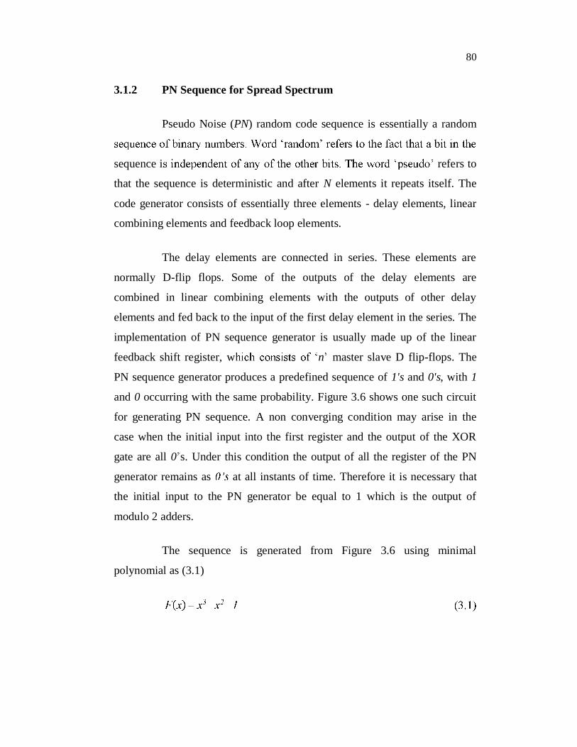
3.1.2 PN Sequence for Spread Spectrum
Pseudo Noise (PN) random code sequence is essentially a random
sequence i refers to
that the sequence is deterministic and after N elements it repeats itself. The
code generator consists of essentially three elements - delay elements, linear
combining elements and feedback loop elements.
The delay elements are connected in series. These elements are
normally D-flip flops. Some of the outputs of the delay elements are
combined in linear combining elements with the outputs of other delay
elements and fed back to the input of the first delay element in the series. The
implementation of PN sequence generator is usually made up of the linear
feedback shift register, w n master slave D flip-flops. The
PN sequence generator produces a predefined sequence of 1's and 0's, with 1
and 0 occurring with the same probability. Figure 3.6 shows one such circuit
for generating PN sequence. A non converging condition may arise in the
case when the initial input into the first register and the output of the XOR
gate are all 0 s. Under this condition the output of all the register of the PN
generator remains as at all instants of time. Therefore it is necessary that
the initial input to the PN generator be equal to 1 which is the output of
modulo 2 adders.
The sequence is generated from Figure 3.6 using minimal
polynomial as (3.1)

81
Figure 3.6 Pseudo noise sequence generator
3.1.3 Direct Sequence Spread Spectrum
The bandwidth expansion in spread spectrum is acquired through a
coding process, e.g. generation of PN sequence codes, that is independent of
the message being sent or the modulation scheme being used. For example,
suppose that a digital signal transmission over a Gaussian channel occupy a
bandwidth B with SNR = 20 dB (i.e. 100 in ratio).
A channel coding scheme can be used to receive data with small
error probability if transmission is carried out at a bit rate less or equal to the
channel capacity C defined by the Equation (3.2) of Shannon s theorem as
given below.
Registers
Output
Mod-2 Adder
REG-R0
REG-R1
REG-R2
REG-R3
+
Clock

82
Substituting for SNR = 20 dB (i.e. 100 in ratio) in Equation (3.2),
gives the ratio of bit rate to bandwidth as shown in (3.3)
Now if SNR is reduce to 10 dB (i.e. 10 in ratio), then referring to
the bandwidth-efficiency diagram, the reliable transmission is still possible at
the same bit rate but with expanded bandwidth is given by (3.4):
Now consider the Equation (3.5) & (3.6)
so that the expansion in the bandwidth is given by (3.7)
thus (3.8)
The original bandwidth has to be expanded by a factor of about
1.9246 to compensate for the reduction in the channel SNR. It can be noted
that increasing the transmission bandwidth will increase the amount of the

83
input noise power in a wideband receiver. This is normally countered by
using a narrowband receiver to limit input noise.
The spread-spectrum concept has developed from the principle of
Shannon s theorem. If data is transmitted at the rate of Rb over a channel
occupying a bandwidth much greater than Rb
that the reliable communication can be achieved at reduced SNR. The
spreading of the energy is achieved by phase modulating the input data with
the user code sequence. The modulation reduces the high power density of the
original data to a low level.
For example, assuming that data is given by (3.9)-(3.11)
m(t) = [1 0 1 0] (3.9)
15-chip code PN sequence is given by
C(t) = [0010 0011 1101 011] (3.10)
then baseband spread spectrum data ms(t) is given by
ms(t) = m(t) C(t) = [0010 0011 1101 011, 1101 1100 0010 100,
0010 0011 1101 011, 1101 1100 0010 100]. (3.11)
This is simple XNOR logical operation between m(t) and C(t).
The received signal has to be converted into the original
narrowband to limit the amount of input noise accompanying the wideband
reception. The conversion is performed at the receiver with the aid of a locally
generated PN code sequence causing the spread spectrum to get compressed
to original length. In the receiver, the received signal is multiplied again by
the same (synchronized) PN code. This operation completely removes the

84
code from the signal and the original data-signal is recovered. This implies
that the despread operation is the same as the spread operation. Space Time
Block Codes (ST-BC) have also been used for DS-CDMA system for
producing hybrid sequence in Shiunn-Jang Chern & Ming-Kai Cheng (2010).
These schemes are used for user verification and signature purposes.
Frequency Hoping CDMA systems are good for band jamming purposes in
Haichang Sui & Zeidler (2007).
Figure 3.7 QPSK modulator for direct sequence spread spectrum CDMA
3.1.4 QPSK Modulator for DS-CDMA
The Quadrature Phase-shift keying (QPSK) is a digital modulation
scheme that transmits data by changing or modulating the phase of a carrier
signal. QPSK uses a finite (four) number of phases each assigned a unique
pattern of binary digits as shown in Figure 3.7. Each pattern of bits forms the
symbol that is represented by the particular phase. QPSK uses four points on
the constellation diagram, equally spaced around a circle. With four phases,
QPSK Signal Binary Data
Stream
0 1 1 0 0 1 0 1 Demultiplexer
Encoder
Encoder x
+
1 0 1 1
0 1 0 0
Multiplier
Multiplier
Eb
- Eb
Eb
- Eb
Q1(t) = (2/Ts) cos ( ct)
Q2(t) = (2/Ts) sin ( ct)
x

85
QPSK can encode two bits per symbol, as shown in Figure 3.8 with gray
coding to minimize the Bit Error Rate (BER).
It can be shown mathematically that QPSK can be used either to
double the data rate compared to Binary Phase Shift Keying (BPSK) or can
reduce the bandwidth by 50 % by keeping the same data rate. This implies
that QPSK transmits twice the data rate in a given bandwidth compared to
BPSK at the same BER. QPSK, however, is more complex to implement. The
functioning and structural concept of QPSK modulator at transmitter is
illustrated in Figure 3.7. and Figure 3.8. The binary data stream is split into
two components - the in-phase and Quadrature-phase components. These are
then separately modulated onto two orthogonal basis functions. In this
implementation, two sinusoids are used. Afterwards, the two signals are
superimposed, and the resulting signal is the QPSK signal. Source encoding is
chosen as polar Non-Return-to-Zero (NRZ). These encoders can be placed
before for binary data source, but have been placed after to illustrate the
conceptual difference between digital and analogue signals involved with
digital modulation
Figure 3.8 Constellation diagram of QPSK using gray coding technique
Quadrature
01 11
10 00In Phase

86
3.1.5 QPSK Demodulator for DS-CDMA
The demodulator, which is designed specifically for the same
symbol-set used by the modulator, determines the phase of the received signal
and maps it to the symbol it represents. Thus the original data is recovered.
This requires the receiver to be able to compare the phase of the received
signal to a reference signal. Such a system is termed coherent system.
Conversely, demodulator can just check for the phase changes alone to
determine the bit received. In that case there is no need for local reference
carrier signal but results in increased BER The typical structure of QPSK
demodulator / receiver is shown in Figure 3.9. The matched filters can be
replaced with correlators. Each detection device uses a reference threshold
value to determine whether a 1 or 0 is detected
Figure 3.9 QPSK demodulator for DS-spread spectrum CDMA communication
0 1 1 0 0 1 0 1
Matched Filter - 1(t)
Matched Filter - 2(t)
Decision Mapping
Multiplexing
Decision Mapping
0 1 0 0
1 0 1 1
Sampling (Ts)
Sampling (Ts)
Binary Data Stream
Received QPSK Signal

87
3.2 IMPLEMENTATION OF DS-CDMA
The DS-CDMA communication system is implemented into FPGA
configuration by 60 inputs for DS-Spread Spectrum and DS-DE-Spread
Spectrum. Thus the simulation are described as the following.
3.2.1 DS-Spread Spectrum
Figure 3.10 shows the simulated results in the form of wave
diagrams of timing events of Spread Stream digital sequence ready for
transmission. The main parameters are chosen as follows: clk with clock
period = 1 millisecond, rst is set to 0. It can be easily explained with the help
of one such experimental result that how it works. Consider one of the inputs
as 1010, and corresponding PN sequence from Figure 3.10 can be found to be
0010 0011 1101 011. The combination is then simulated. This results in de-
spreading data sequence of 60 bit length. The spread sequence in this example
is found to be 0010 0011 1101 011 1101 1100 0010 100 0010 0011 1101 011
1101 1100 0010 100 which is represented by tag named spread_data (59:0).
This is the final spread data to be modulated by using QPSK modulation
scheme and then to be transmitted. The QPSK scheme required an even
number of bits in the spread sequence. It will then take a pair of bits and map
the pair with one of the four quadrants according to the values of the bits for
gray code scheme as shown in the Figure 3.8. This is called symbol mapping.
The mapped symbols are transmitted further to the channel which may have
noise.

88
Figure 3.10 DS-Spread stream results on XILINX FPGA

89
3.2.2 DS-De-Spread Sequence
De-spreading is reverse process of spreading. This implies that
from de-spreading sequence, the original message bits are to be extracted.
Figure 3.11 shows the simulated results in the form of waveforms of timing
diagram for de-spreading digital sequence stream received at receiver by
using locally generated PN-sequence and de-spreading algorithm. The main
parameters are chosen as follows: clk with clock period = 1 millisecond, rst is
set to 0. The output is the original message data recovered. To explain the
working of the receiver for de-spreading operation an experimental result may
be illustrated. Assuming that a 60 bit long input spread sequence received by
receiver is 0010 0011 1101 011 0010 0011 1101 011 0010 0011 1101 011
1101 1100 0010 100. This sequence is operated upon by locally generated PN
sequence, in this example is 0010 0011 1101 011, which was also used at
transmitter for spreading. After simulation, the extracted message data is
found to be 1110, clearly as shown in Figure 3.11. Similarly further,
additional tests are carried out to check the effectiveness of implemented de-
spreading algorithm circuit for message data of 0000, 0001, 0101, 0110, 1001,
1010, 1110 and 1111. All of these message data spreading and de-spreading
are clearly illustrated by Figure 3.11. This verifies that any binary spread
spectrum communication system can be implemented by scaling up the
procedure explained in this project. The experimental results can be verified
as shown in the Table 3.1, that this is very simple and less complex design as
a very few gates and logic slices are used by circuit when implemented on
FPGA chip.

90
Figure 3.11 Receiver results after de-spreading and demodulating received data from a noisy channel

91
3.3 RESULT ANALYSIS
The results of QPSK modulation implemented on MATLAB
Communication Tool box are shown in Figure 3.12. The input sequence is
[0010 0011 1101 011 1101 1100 0010 100 0010 0011 1101 011 1101 1100
0010 100].
Figure 3.12 Mapping of spread message data into QPSK symbols while transmitting and de-mapping at receiver

92
The modulated binary bit pairs are converted into 4 symbols as shown in y-
axis. 60 bit long message data stream is converted into 30 symbols of
information by QPSK. The results of QPSK demodulation implemented on
MATLAB Communication Tool box are also shown in Figure 3.12. The input
sequence is firstly assumed to be noise free or ideal and then it is QPSK
demodulated using MATLAB and C codes.
Table 3.1 Summary of logic device utilization on FPGA
Slice Logic Utilization Used Available Utilization Number of Slice Registers 6 93,120 1%
Number used as Flip Flops 6
Number of Slice LUTs 3 46,560 1%
Number used as logic 1 46,560 1%
Number using O6 output only 1
Number used exclusively as route-thrust 2
Number with same-slice register load 2 Number of occupied Slices 3 11,640 1%
Number of LUT Flip Flop pairs used 4
Number with an unused LUT 1 4 25%
Number of fully used LUT-FF pairs 3 4 75% Number of unique control sets 2
Number of slice register sites lost to control set restrictions 10 93,120 1%
Number of bonded IOBs 7 240 2%
Number of BUFG/BUFGCTRLs 1 32 3%
Number used as BUFGs 1
Number of STARTUPs 1 1 100%
Average Fan-out of Non-Clock Nets 4.67

93
Results at receiver verify mapping of the same sequence which was
transmitted. The recovered sequence is [0010 0011 1101 011 1101 1100 0010
100 0010 0011 1101 011 1101 1100 0010 100], as shown in Figure 3.12. This
is the same sequence which was transmitted. The two binary bits (a pair) are
converted into one of the 4 symbols. Figure 3.12 shows the constellation
diagram for QPSK demodulator while considering that there was no noise in
the channel which is ideal case and for which there is no observed phase
distortion. The recovered data at receiver is interpreted as 1010 as shown in
Figure 3.11. The performance of the implemented sub- systems of proposed
DS-CDMA communication system is analyzed based on the number of gates
or devices utilized. The summary is presented as shown in Table 3.1.
Implementation is carried out on XILINX FPGA chip type xc6vlx75t-3ff484
and simulation is executed using ISE 12.1 version software EDA tool from
XILINX.
The fundamental concept used for transmitter and receiver
hardware of cellular communication system is implemented for CDMA
scheme. Transceiver is realized by developing VHDL codes and testing the
same for a wide range of input conditions. The logic implemented is very
simple and faster. A 15-bit chip rate (PN sequence 1001 0001 1110 101) is
realized by shifting the input through the D-flip flops. A minimal polynomial
property is made compulsory so that PN sequence repeats after a cycle of chip
code length (15 in this case). The PN sequence is achieved by providing
feedback from the outputs of some of the registers (called taps) according to
minimal polynomial used. The feedback is then fed back into the most
significant register after passing them through a modulo-2 adder circuit. The
process of realizing LFSR is carried out by first developing the VHDL code
for a D-flip flop. The same D- flip flop code is then called 4 times in the main
VHDL program to realize the required LFSR. In the implementation part of
PN sequence, tapings are taken from 1st, 3rd and 4th positions of LFSR so as to

94
obtain the maximum length of binary digits produced before they are being
repeated. A dead lock condition is observed in the case when the initial input
into the first register and output of the XOR gate are all 0 . Under this
condition the output of all the register of the LFSR PN generator remains as 0
at all instants of time. Therefore it is necessary that the initial input to the PN
generator must be equal to 1 which is also the output of the modulo-2 circuit.
The VHDL code for implementing all subsystem circuits of transceiver are
simulated on XILINX ISim and Model Sim and hence, the results were
generated and tested successfully for a wide variety of message data selected
randomly. Implementation was done using XILINX FPGA with clock
frequency of 100 MHz range.
3.4 SUMMARY
In this chapter, a typical CDMA transceiver has been analyzed with
particular attention of modulation, demodulation, spreading, de-spreading on
FPGA and also typical CDMA transceiver effects that must be considered in
the design of a CDMA system on FPGA. One can analyze a number of gates,
slice register, Logic Utility Device and so on in FPGA.