Embed Size (px)
Citation preview
33
Chapter 3
Conformal Mapping Technique
Various techniques have been used to calculate the conductor loss, including
Wheeler's incremental inductance rule [26], closed-form formulae based on rigorous
numerical techniques and interpolation [27], perturbation methods combined with the
conformal mapping technique [28-35], quasi-static and full-wave approaches based
on the spectral domain method (SDM) [36], integral equation method (IEM) [37],
finite element method (FEM) [38], mode-matching method (MMM) [39, 40], etc.
When the conductor thickness is the order of the skin depth, traditional quasi-analytic
Wheeler's incremental inductance rule and classical conformal mapping models be-
come inadequate to characterize the attenuation, since they assume the conductor
thickness is much larger than the skin depth. Rigorous quasi-static and full-wave
numerical techniques give accurate frequency dependent parameters, such as charac-
teristic impedance and complex propagation constant from DC to high frequency, but
these are numerically intensive and time-consuming.
Recently, an efficient quasi-static technique has been developed to calculate the
conductor loss by using the conformal mapping technique [21, 22], which is based on
quasi-TEM approximation. This technique was applied to a coplanar waveguide
(CPW) and symmetric twin conductors, and calculated resistance agreed well to ex-
perimental data for all frequencies. This technique is accurate for mirror symmetric
structures, even though good results were obtained for the asymmetric structure of a
coplanar waveguide (CPW). In the previous work the conductor thickness was as-
sumed zero in the conformal mapping procedure and the surface impedance of a flat
34
conductor (i.e., position independent) was used for the effective internal impedance
all over the conductor surfaces in case of a coplanar waveguide (CPW). In this chap-
ter, this technique will be applied to examples of a microstrip line and a V-shaped
conductor backed coplanar waveguide (VGCPW), while considering the conductor
thickness in the conformal maps and using the EII of thick rectangular conductors.
The calculated resistance and inductance are compared to the results of more rigorous
quasi-static solutions. And it is explained that the effective internal impedance (EII)
approximates the standard impedance boundary condition (SIBC) and this technique
gives a reasonable approximation in the asymmetric problems of a microstrip and a
V-shaped conductor backed coplanar waveguide (VGCPW).
3.1 Conformal Mapping and Partial Differential Equations
A point in the w-plane can be related to a given point in the z -plane with a func-
tion. Any point (x, y) in the z -plane yields some point (u,v) in the w-plane, and the
function that accomplishes this is called a coordinate transformation from the z -plane
to w-plane. If the function consists of complex variables and is analytic, then a
complex plane of z = x + jy is transformed into another complex plane of w = u + jv ,
and the infinitesimal shape is preserved during the transformation. This is called a
conformal map, and the Cauchy-Riemann conditions of (3.1) is a sufficient and nec-
essary condition for that function to be a conformal map.
∂u
∂x= ∂v
∂y
∂u
∂y= − ∂v
∂x
(3.1)
A conformal map can transform a complicated domain to a simple domain
through a given function;
35
w = f (z) (3.2)
And a potential function φ that is a solution to the Laplace equation defined in the z -
plane can be converted to a potential function ψ defined in the w-plane. By invok-
ing the Cauchy-Riemann conditions to replace variable z in φ by w , the invariance
of Laplace equation under a conformal transformation is shown in the reference [41]
by
∂ 2φ x, y( )∂x2 + ∂ 2φ x, y( )
∂y2 = 1
M2∂ 2ψ u,v( )
∂u2 + ∂ 2ψ u,v( )∂v2
= 0 (3.3)
M = dw
dz
where M is a scaling factor that is the derivative of the mapping function with re-
spect to z . These transformations can be done through any number of intermediate
steps to get a simpler and more readily analyzable configuration, and many physical
problems that depend on the Laplace equation can be easily solved. Therefore, find-
ing a complex function mapping the original domain into the simple domain replaces
solving a Laplace equation in original domains. Many transmission lines have been
analyzed using conformal maps to give characteristic impedance and effective permit-
tivity in case of lossless thin conductors.
For the lossy conductor of finite conductivity and finite thickness, the conformal
map should transform the region inside of the conductor as well as outside of the con-
ductor to consider the field penetration into the conductor. And a scalar Helmholtz
equation is added as a governing partial differential equation inside the conductor as
well as the Laplace equation outside of the conductor. The Helmholtz equation is
modified under the transformations to become
36
∇xy2 J(x, y) − jωµσJ(x, y) = 1
M2 ∇uv2 J(u,v) − jωµσM2 J(u,v)( ) = 0 (3.4)
where a complicated inhomogeneous conductivity should be considered in the
mapped domain. The simplification of the boundaries is accompanied by the com-
plexity of inhomogeneous conductor material properties, and this trade-off makes it
as hard to analyze lossy transmission lines in the mapped domains as it was in the
original domains.
The perturbation method combined with the conformal mapping technique can be
used to calculate the conductor loss [28-35], but these techniques are valid only at
high frequency where the conductor thickness is larger than the skin depth. In the
following section, a method using the conformal mapping technique is presented
which can find the conductor loss from low frequency where the conductor thickness
is on the order of the skin depth or less to high frequency where the skin and proxim-
ity effect are fully developed.
3.2 Conductor Loss Calculation using Conformal Mapping
Technique
To accurately predict frequency dependent resistance and inductance the model
should account for not only current crowding towards the surface and edges of the
conductor due to the skin and proximity effect at high frequency, but also uniform
current distribution at low frequency. To avoid conformal maps inside of the conduc-
tor and properly consider the frequency dependent skin depth, a complex EII is de-
fined on the surface of the conductor, which represent resistance and internal induc-
tance of conductors and is determined by the frequency and the geometry, permittiv-
37
ity, permeability, and conductivity of the isolated conductor. And to account for the
current crowding induced by the interaction between and inside of the conductors
(i.e., the proximity effect), a conformal map transforms the complicated real space
domain into a simple domain and the transverse resonance method is then applied.
This approach is valid up to the frequency where the quasi-TEM assumption is ap-
propriate, and the calculation of capacitance and effective permittivity is decoupled
from the calculation of resistance and inductance.
y
z-plane
w-plane
vt
vb
v
0 du(u,vb)
du(u,vt)
dz(x',y')
dz(x,y)
t-plane
dt(t) dt(t')0 0
x
uo u
t
ξz=f(t)
w=g(t)
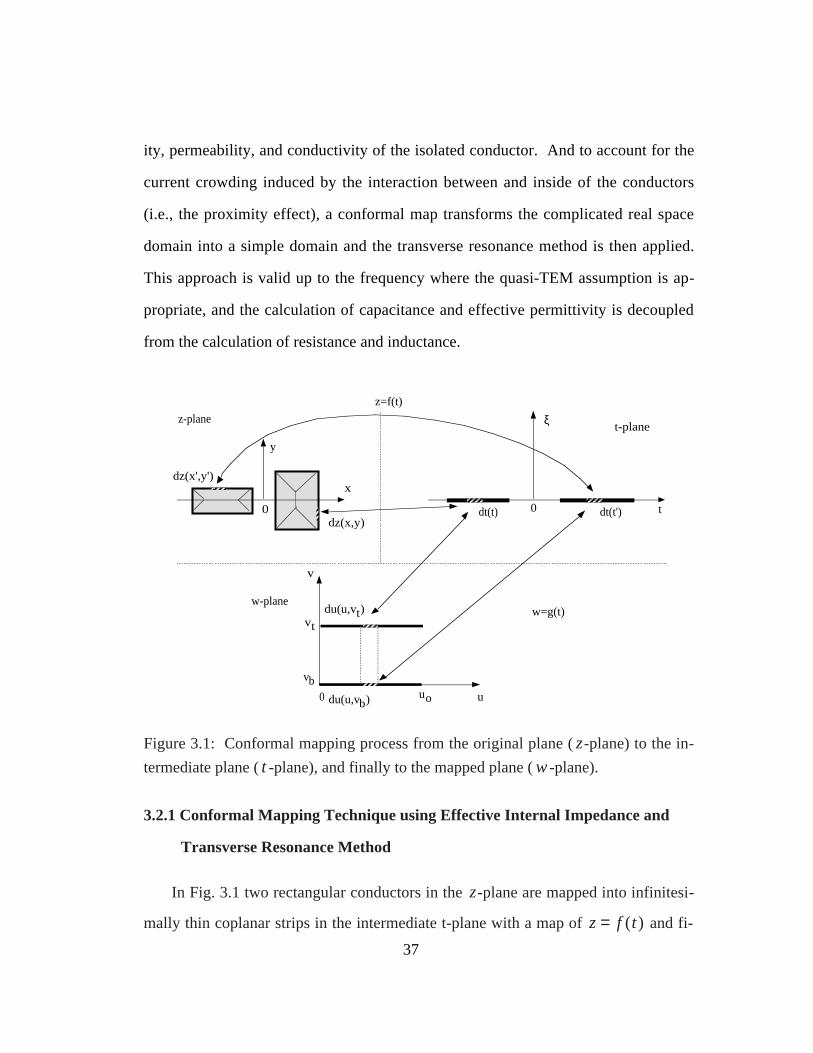
Figure 3.1: Conformal mapping process from the original plane ( z-plane) to the in-
termediate plane ( t -plane), and finally to the mapped plane ( w -plane).
3.2.1 Conformal Mapping Technique using Effective Internal Impedance and
Transverse Resonance Method
In Fig. 3.1 two rectangular conductors in the z-plane are mapped into infinitesi-
mally thin coplanar strips in the intermediate t-plane with a map of z = f (t) and fi-

38
nally mapped into parallel plates in the w -plane with a map of w = g(t). A point
(x, y) on the surface of the conductor with corresponding EII of Zeii (x, y) maps onto
a point in the w -plane at (u,vt ) on the top plate. The EII is scaled in the w -plane by
M(u,vt )Zeii (x, y) = M(u,v)Zeii (Re f (g−1(u,vt )), Im f (g−1(u,vt ))) (3.5)
where M is a scaling factor, g−1(u,v) is the inverse of the mapping function, and
(u,vt ) is a point on the top plate. The differential series impedance per unit length
dZtop of the top plate due to a differential width du is then
dZtop = M(u,vt )Zeii (u,vt )du
(3.6)
where Zeii is the EII at some point (x, y) in the z-plane corresponding to a given
point (u,vt ) in the w -plane. With the same procedure the differential series
impedance per unit length dZbot of the bottom plate due to a differential width du is
dZbot = M(u,vb )Zeii (u,vb )du
(3.7)
where (u,vb ) is a point on the bottom plate. Assuming uniform magnetic fields be-
tween two plates and using the transverse resonance technique, the inductance due to
a differential width du and a separation vt − vb is given by
dL =µo vt − vb
du(3.8)
where µ0 is the permeability of free space. Finally, the total differential series
impedance per unit length is
dZtot = dZtop + dZbot + jωdL (3.9)
39
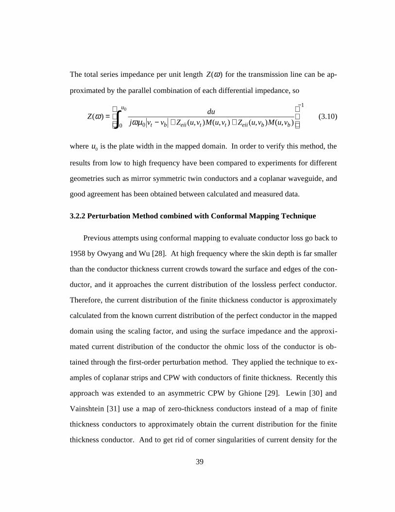
The total series impedance per unit length Z(ω ) for the transmission line can be ap-
proximated by the parallel combination of each differential impedance, so
Z(ω ) = du
jωµ0 vt − vb + Zeii (u,vt )M(u,vt ) + Zeii (u,vb )M(u,vb )0
u0
∫
−1
(3.10)
where u0 is the plate width in the mapped domain. In order to verify this method, the
results from low to high frequency have been compared to experiments for different
geometries such as mirror symmetric twin conductors and a coplanar waveguide, and
good agreement has been obtained between calculated and measured data.
3.2.2 Perturbation Method combined with Conformal Mapping Technique
Previous attempts using conformal mapping to evaluate conductor loss go back to
1958 by Owyang and Wu [28]. At high frequency where the skin depth is far smaller
than the conductor thickness current crowds toward the surface and edges of the con-
ductor, and it approaches the current distribution of the lossless perfect conductor.
Therefore, the current distribution of the finite thickness conductor is approximately
calculated from the known current distribution of the perfect conductor in the mapped
domain using the scaling factor, and using the surface impedance and the approxi-
mated current distribution of the conductor the ohmic loss of the conductor is ob-
tained through the first-order perturbation method. They applied the technique to ex-
amples of coplanar strips and CPW with conductors of finite thickness. Recently this
approach was extended to an asymmetric CPW by Ghione [29]. Lewin [30] and
Vainshtein [31] use a map of zero-thickness conductors instead of a map of finite
thickness conductors to approximately obtain the current distribution for the finite
thickness conductor. And to get rid of corner singularities of current density for the
40
zero-thickness conductor, the integration in loss calculation was carried out upto
some distance away from the edges. Referring to Collin [32], the resistance of two
conductors can be calculated from the real part of the equation
Z(ω ) = 1
Itot2 ZsJs ⋅ Js
∗dlklk∫
k=1
2
∑
+ jωLext , (3.11)
where Zs is the surface impedance, lk is the periphery of each conductor, Js is the
surface current density, and Lext is the external inductance. At high frequency the
current density of the perfect conductor is uniform in the mapped parallel plates and
the current density is approximated using the scaling factor by
J(x, y) = Itot M
uo, (3.12)
where M is a scaling factor at (u,vt ) or (u,vb ) on the mapped parallel plate corre-
sponding to (x, y) in original domain. At high frequency the surface impedance of
the flat conductor tends to (2.2). Except in the neighborhood of the conductor edges,
(2.2) is appropriate all over the conductor. Since the current distribution approxi-
mates that of the perfect conductor, to avoid overestimation error near the edges the
position independent surface impedance of (2.2) is used in the vicinity of the edges as
well as on the flat surface of the conductor. And the total series impedance is given by
Z(ω ) = 1 + j
σδuo2 (M(u,vt ) + M(u,vb ))
0
u0
∫
+ jωµo vt − vb
uo, (3.13)
where the second term denotes the external inductance of the transmission line.
Recently, Kuester et al. [33, 34] have modified this technique using a generalized
transfer impedance boundary condition [17] instead of a standard SIBC to take care of
41
the interaction between top and bottom sides of the conductors at low frequency, and
have numerically calculated the stopping distance with respect to various frequencies
and two edge shapes. The results are good at high frequency and reasonable for an
example of a CPW at low frequency where the conductor thickness is the order of the
skin depth or less, but this modification can not accommodate general structures of
various transmission lines in that the stopping distance must be a priori determined at
every frequency of concern and the current distribution of the perfect conductor is not
useful to represent the low frequency current distribution of a conductor having finite
conductivity.
On the other hand, Schinzinger and Ametani [35] applied the conformal mapping
technique to an eccentric coaxial line and a round wire over a ground plane. This
procedure gives an equation of similar form to (3.13). But to avoid point by point
evaluation of the scaling factor they use an averaged scaling factor and, therefore, av-
eraged surface impedance in the mapped domain. This can result in significant inac-
curacy especially in case of conductors that are closely coupled and in which the
proximity effect is dominant.
3.2.3 High Frequency and Low Frequency Limit
In (3.9), EII always tends to (3.14) as the frequency increases, (it is identical to
(2.2))
Zeiihf = jωµ
σ= 1 + j
σδ, (3.14)
where δ is the skin depth in the conductor. It defines the surface impedance all over
the conductor surface except the edges and becomes position independent. With this
42
substitution, the high frequency series impedance per unit length for the transmission
line is derived from (3.10) to be
Zhf (ω ) = 1 + j
σδuo2 (M(u,vt ) + M(u,vb ))
0
u0
∫
+ jωµo vt − vb
uo, (3.15)
where the second term corresponds to the external inductance, and the real term of
(3.15) is the resistance of the transmission line. Note this expression is exactly the
same as (3.13) and, therefore, at high frequency the proposed method is said to in-
clude the previous perturbation methods combined with the conformal mapping tech-
nique.
As ω → 0 (i.e., at low frequency), (3.10) becomes
Zlf (ω ) = du
ZeiiM(u,vt ) + ZeiiM(u,vb )0
u0
∫
−1
+ jωµ0 vt − vb (3.16)
⋅ du
(ZeiiM(u,vt ) + ZeiiM(u,vb ))20
u0
∫
du
ZeiiM(u,vt ) + ZeiiM(u,vb )0
u0
∫
−2
If the two conductors are symmetric (i.e., two conductors have identical cross-sec-
tions and there exists a line of mirror symmetry between them), then
M(u,vt ) = M(u,vb ), Zeii (u,vt ) = Zeii (u,vb ) , and the real term of (3.16) can be re-writ-
ten as
Zlf (ω ) = 2du
ZeiiM(u,vt )0
u0
∫
−1
+ jωµ0 vt − vb (3.17)
⋅ du
M2(u,vt )0
u0
∫
du
M(u,vt )0
u0
∫
−2
43
And, therefore, the total DC resistance per unit length is
Rdc = 2Rs (0)du
M(u,vt )0
u0
∫
−1
(3.18)
where Rs (0) = ReZeii (ω = 0)
But for an asymmetric transmission line (3.17) gives low frequency resistance with
some error. To compensate for this error, the real term of (3.10) can be normalized
by the actual DC resistance of the asymmetric conductors.
At low frequency, the current distribution is dominantly determined by resis-
tance. Therefore, if the perturbational expression of the series impedance is valid at
low frequency, then (3.11) becomes
Zlf (ω ) = du
ZeiiM(u,vt )0
u0
∫
−1
+ du
ZeiiM(u,vb )0
u0
∫
−1
+ jωµ0vt − vb
uo. (3.19)
The real term of (3.19) gives the low frequency resistance of the transmission line,
even though the imaginary term may give poor low frequency inductance. If the
transmission line is symmetric and EII substitutes as the surface impedance, then the
real term of (3.19) is the same as the real term of (3.17).
3.3 Examples
A simple example is the case of parallel rectangular conductors. One configura-
tion is to put two conductors in parallel as in a parallel plate waveguide, and another
configuration is to put them side by side as in coplanar strips. A new type of V-
shaped conductor-backed coplanar waveguide (VGCPW) is also analyzed, and a
normal coplanar waveguide (CPW) and microstrip lines of normal structure and V-
44
shaped ground are analyzed and compared with each other. The results are compared
to more rigorous solutions of the volume filament method (VFM) [24] and the surface
ribbon method (SRM) [21, 22]
3.3.1 Symmetric Twin Rectangular Conductors
For conductors with rectangular cross-section a conformal map is guaranteed to
exist, based on a Schwarz-Christoffel transformation. Two rectangular conductors
can be mapped into parallel plates by two steps of maps. The first map transforms two
conductors from the z-plane into two thin, coplanar strips in the t -plane
z(t) = c(ξ 2 −1 / k1
2 )(ξ 2 −1 / k22 )
(ξ 2 −1)(ξ 2 −1 / k2 )0
t
∫ dξ , (3.20)
where c, k1, k2 , and k are mapping coefficients and are determined by the separation,
width and thickness of the conductors. The second map converts the coplanar strips
in the t -plane to the parallel plates in the w -plane
w(t) = dξ(ξ 2 −1)(ξ 2 −1 / k2 )0
t
∫ . (3.21)
The scale factor from the z-plane to the intermediate t -plane is
M(t) = dt
dz= 1
c
(t2 −1)(t2 −1 / k2 )
(t2 −1 / k12 )(t2 −1 / k2
2 )(3.22)
and the scale factor from t -plane to w -plane is
N(t) = dt
dw= (t2 −1)(t2 −1 / k2 ) . (3.23)
And the series impedance per unit length Z(ω ) is given by
45
Z(ω ) = dξjωµo vt − vb N(ξ ) + 2Zeii (ξ )M(ξ )1
1/k
∫
−1
(3.24)
To compare between results using different EIIs, both the plane wave model and the
transmission line model are used to calculate the series impedance.
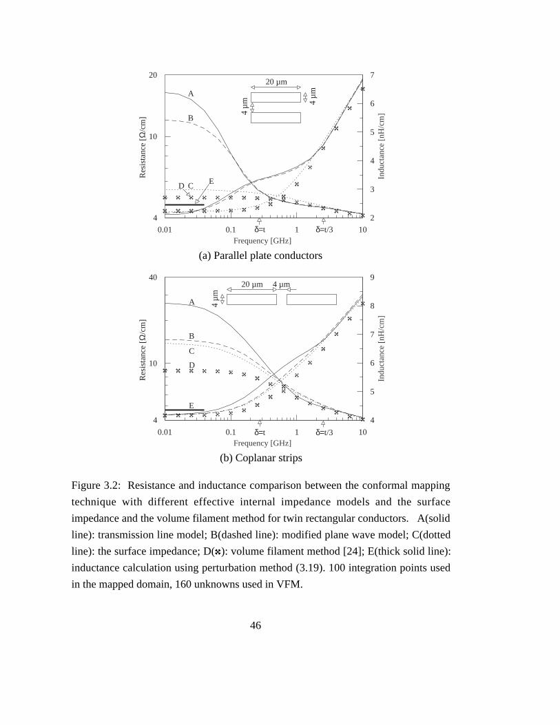
Figure 3.2(a) shows results for a closely coupled parallel plate structure with
thickness of 4 µm, width of 20 µm, gap of 4 µm, and conductivity of 5.8 ×10⁷S/m.
Calculated resistance and inductance at high frequency (where δ < t / 3) and low fre-
quency resistance agree well with results of the volume filament method regardless of
the EII model used. At mid frequency, resistance using EII models are overestimated
by around 30%, and low frequency inductance (the least important parameter) are
also overestimated by 25% and 95%, respectively. Figure 3.2(b) shows results for
closely coupled coplanar strips with thickness of 4 µm, width of 20 µm, gap of 4 µm,
and conductivity of 5.8 ×10⁷S/m. Again, calculated resistance and inductance at
high frequency and low frequency resistance agree well with results of the volume
filament method. At mid frequency resistance using the modified plane wave model
gives good agreement within a few percent, the resistance using the transmission line
model is overestimated by around 20%, and low frequency inductance is also overes-
timated by 20% using the modified plane wave model and 40% using the transmis-
sion line model. For both examples the surface impedance of the coupled conductors,
which is numerically calculated using the volume filament method, has been used and
resistance is in good agreement with that of the volume filament method for all fre-
quencies. Since (3.19) assumes uniform flux between the parallel plates in the
mapped domain at all frequencies it underestimates low frequency inductance. In
(3.10) uniform flux is assumed between the parallel plates with differential width of
46
4
10
20
2
3
4
5
6
7
0.01 0.1 1 10
Indu
ctan
ce [
nH/c
m]
Frequency [GHz]
Res
ista
nce
[Ω/c
m]
δ=t δ=t/3
A
B
CD E
20 µm
4 µm
4 µm
(a) Parallel plate conductors
4
10
40
4
5
6
7
8
9
0.01 0.1 1 10
Indu
ctan
ce [
nH/c
m]
Frequency [GHz]
Res
ista
nce
[Ω/c
m]
δ=t δ=t/3
20 µm 4 µm
A
B
C
D
E
4 µm
(b) Coplanar strips
Figure 3.2: Resistance and inductance comparison between the conformal mapping
technique with different effective internal impedance models and the surface
impedance and the volume filament method for twin rectangular conductors. A(solid
line): transmission line model; B(dashed line): modified plane wave model; C(dotted
line): the surface impedance; D(8): volume filament method [24]; E(thick solid line):
inductance calculation using perturbation method (3.19). 100 integration points used
in the mapped domain, 160 unknowns used in VFM.
47
0
1
2
3
4
0 0.2 0.4 0.6 0.8 1
Nor
mal
ized
|Zs|
Normalized u-axis
0
1
A
B
C
(a) At the skin depth δ=5t
0
1
2
3
4
0 0.2 0.4 0.6 0.8 1
Nor
mal
ized
|Zs|
Normalized u-axis
0
1
AB
C
(b) At the skin depth δ=t/2
0
1
2
3
0 0.2 0.4 0.6 0.8 1
Nor
mal
ized
|Zs|
Normalized u-axis
0
1
A
BC
(c) At the skin depth δ=t/6
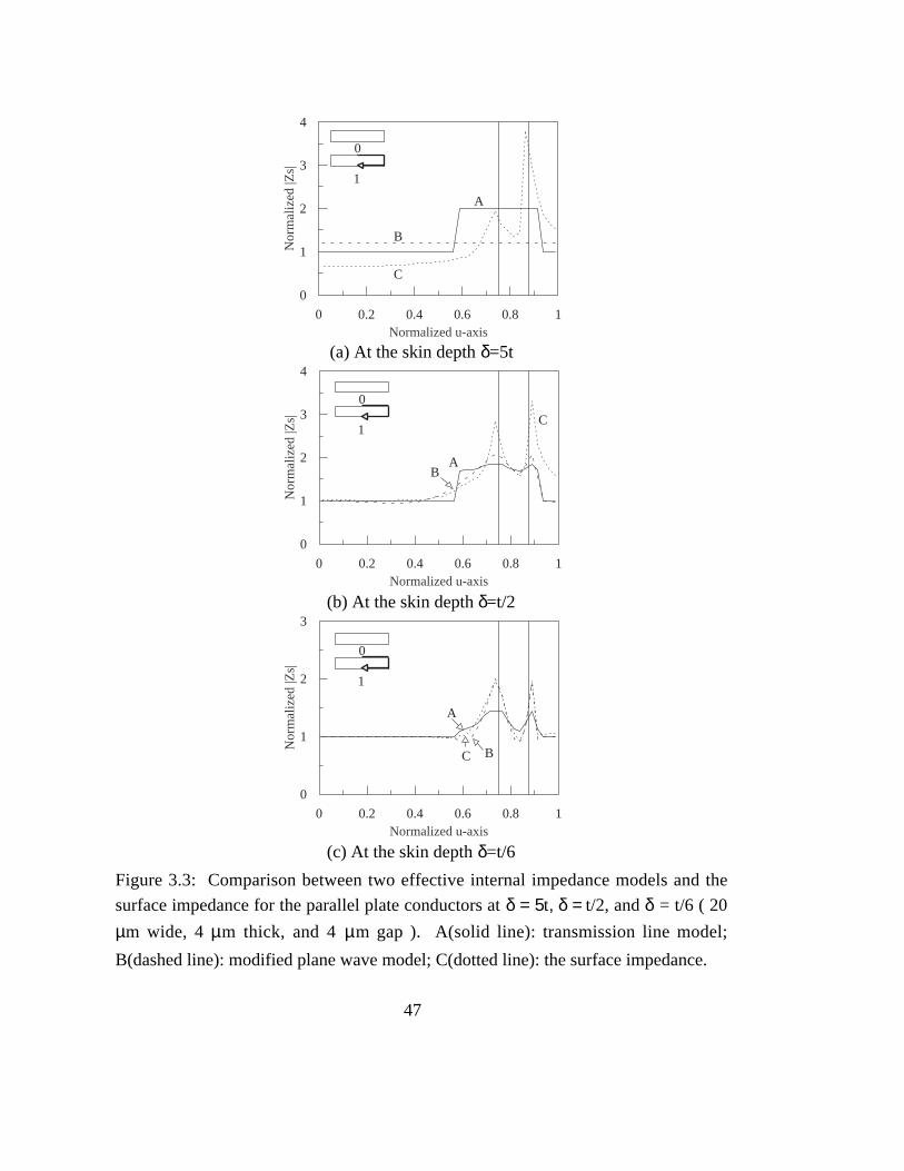
Figure 3.3: Comparison between two effective internal impedance models and the
surface impedance for the parallel plate conductors at δ = 5t, δ = t/2, and δ = t/6 ( 20
µm wide, 4 µm thick, and 4 µm gap ). A(solid line): transmission line model;
B(dashed line): modified plane wave model; C(dotted line): the surface impedance.
48
du in the mapped domain at low frequency, and it also overestimates the low fre-
quency inductance. For both examples the results using the surface impedance give
the best answers at all frequencies, but in reality the surface impedance calculation is
as intensive as the field calculation and, therefore, EII (an approximation of the sur-
face impedance of an isolated conductor) can be used as an approximation with some
tolerable error. For these examples the modified plane wave model gives better re-
sults than the transmission line model.
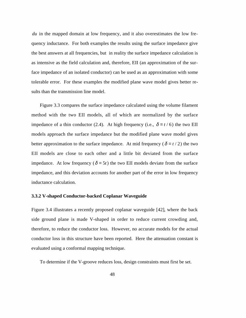
Figure 3.3 compares the surface impedance calculated using the volume filament
method with the two EII models, all of which are normalized by the surface
impedance of a thin conductor (2.4). At high frequency (i.e., δ = t / 6) the two EII
models approach the surface impedance but the modified plane wave model gives
better approximation to the surface impedance. At mid frequency (δ = t / 2) the two
EII models are close to each other and a little bit deviated from the surface
impedance. At low frequency (δ = 5t ) the two EII models deviate from the surface
impedance, and this deviation accounts for another part of the error in low frequency
inductance calculation.
3.3.2 V-shaped Conductor-backed Coplanar Waveguide
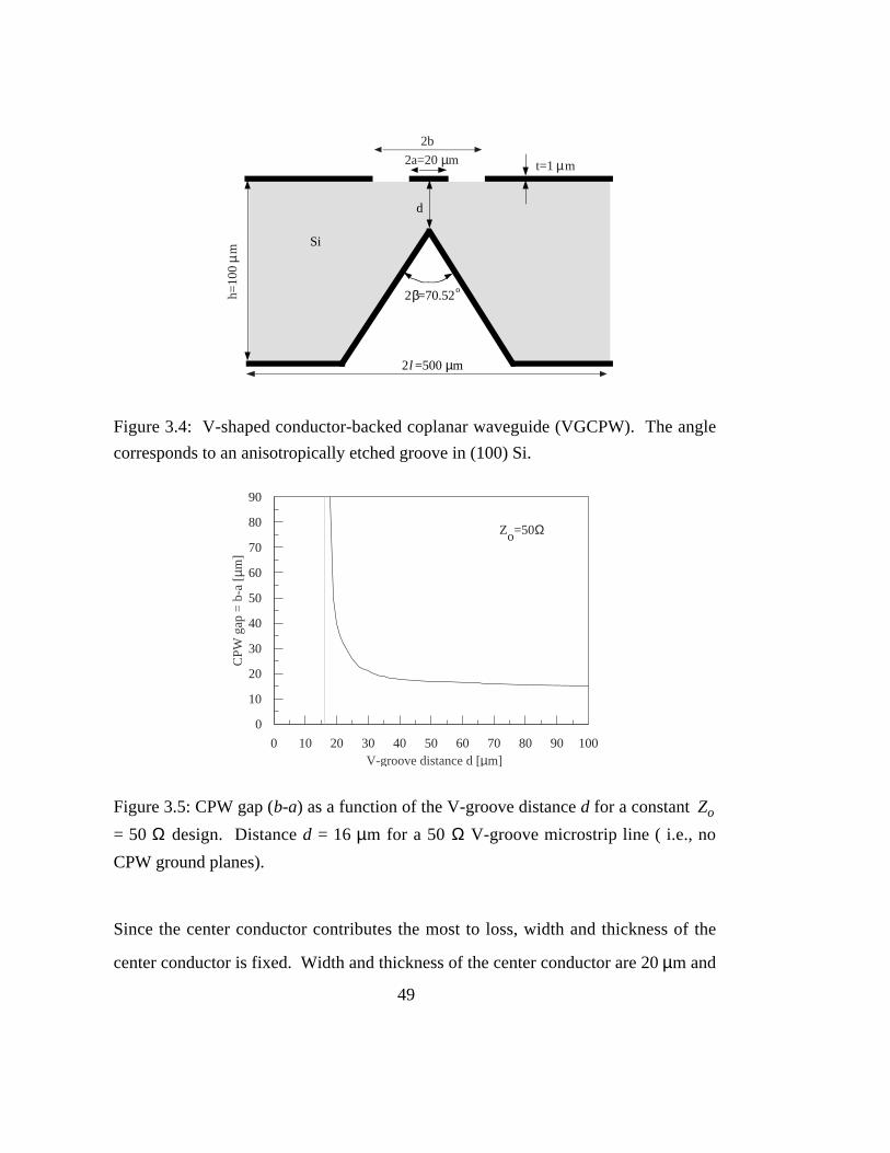
Figure 3.4 illustrates a recently proposed coplanar waveguide [42], where the back
side ground plane is made V-shaped in order to reduce current crowding and,
therefore, to reduce the conductor loss. However, no accurate models for the actual
conductor loss in this structure have been reported. Here the attenuation constant is
evaluated using a conformal mapping technique.
To determine if the V-groove reduces loss, design constraints must first be set.
49
Sih=
100
µm
2a=20 µm
2b
t=1 µm
2β=70.52
d
o
2l =500 µm
Figure 3.4: V-shaped conductor-backed coplanar waveguide (VGCPW). The angle
corresponds to an anisotropically etched groove in (100) Si.
0
10
20
30
40
50
60
70
80
90
0 10 20 30 40 50 60 70 80 90 100
CPW
gap
= b
-a [
µm]
V-groove distance d [µm]
Zo=50Ω
Figure 3.5: CPW gap (b-a) as a function of the V-groove distance d for a constant Zo
= 50 Ω design. Distance d = 16 µm for a 50 Ω V-groove microstrip line ( i.e., no
CPW ground planes).
Since the center conductor contributes the most to loss, width and thickness of the
center conductor is fixed. Width and thickness of the center conductor are 20 µm and
50
1 µm, respectively, and the conductivity of metal is 5.8 ×10⁷S/m, the substrate is
high resistivity Si, so dielectric loss is ignored, and the relative permittivity of Si is
11.7. The location of the CPW ground plane (i.e., b) for a specified V-groove (i.e., d
and h are given) is determined to maintain a high frequency characteristic impedance
of 50 Ω. To get designs of 50 Ω characteristic impedance, capacitance is calculated
using conformal mapping by assuming the air-dielectric boundary is a perfect mag-
netic wall. The calculated capacitance is compared to the result using the boundary
element method (BEM) [43, 44]; the conformal map result considering the thickness
of conductors agreed with BEM results to within a few percent (< 2.5%) up to the
fairly wide gap (b - a) of 90 µm. Figure 3.5 shows the resulting gap (b - a) necessary
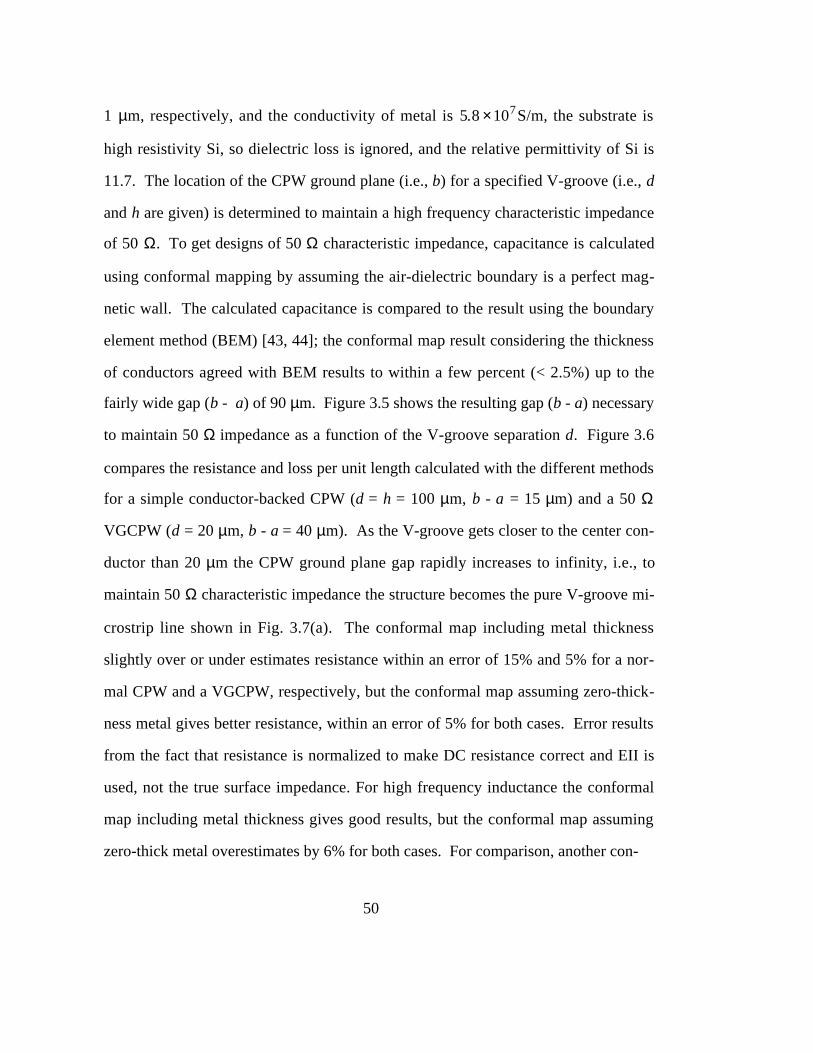
to maintain 50 Ω impedance as a function of the V-groove separation d. Figure 3.6
compares the resistance and loss per unit length calculated with the different methods
for a simple conductor-backed CPW (d = h = 100 µm, b - a = 15 µm) and a 50 Ω
VGCPW (d = 20 µm, b - a = 40 µm). As the V-groove gets closer to the center con-
ductor than 20 µm the CPW ground plane gap rapidly increases to infinity, i.e., to
maintain 50 Ω characteristic impedance the structure becomes the pure V-groove mi-
crostrip line shown in Fig. 3.7(a). The conformal map including metal thickness
slightly over or under estimates resistance within an error of 15% and 5% for a nor-
mal CPW and a VGCPW, respectively, but the conformal map assuming zero-thick-
ness metal gives better resistance, within an error of 5% for both cases. Error results
from the fact that resistance is normalized to make DC resistance correct and EII is
used, not the true surface impedance. For high frequency inductance the conformal
map including metal thickness gives good results, but the conformal map assuming
zero-thick metal overestimates by 6% for both cases. For comparison, another con-
51
Res
ista
nce
[Ω/c
m]
8
10
30
4
5
6
7
0.01 0.1 1 10 50
Indu
ctan
ce [
nH/c
m]
Frequency [GHz]
A
B
C
D
E
0
0.5
1
1.5
2
2.5
3
0.01 0.1 1 10 50Frequency [GHz]
Atte
nuat
ion
cons
tant
α[d
B/c
m]
A
BC
D
E
(a) (b)
(a) Resistance and inductance and (b) attenuation constant for a 50 Ω CPW ( a = 10
µm, b = 25 µm, and d = h = 100 µm ).
8
10
30
4
5
6
7
0.01 0.1 1 10 50
Indu
ctan
ce [
nH/c
m]
Frequency [GHz]
Res
ista
nce
[Ω/c
m]
A
B
C
D
E
0
0.5
1
1.5
2
2.5
0.01 0.1 1 10 50Frequency [GHz]
Atte
nuat
ion
cons
tant
α[d
B/c
m]
A
BC
D
E
(c) (d)
(c) Resistance and inductance and (d) attenuation constant for a 50 Ω CPW ( a = 10
µm, b = 50 µm, d = 20 µm, and h = 100 µm ).
Figure 3.6: Comparison of various modeling techniques for the conductor loss of a
50 Ω CPW and a 50 Ω VGCPW. A(solid line): conformal map assuming conductor
thickness is zero; B(dotted line): conformal map of finite thickness conductors,;
C(dashed line): surface ribbon method [21, 22]; D(8): volume filament method [24];
E(thick solid line): perturbation method (3.13).
52
. .
Si
h=10
0 µ
m
w=20 µm
2l =500 µm
t=1 µm
2β=70.52o
d=16 µm
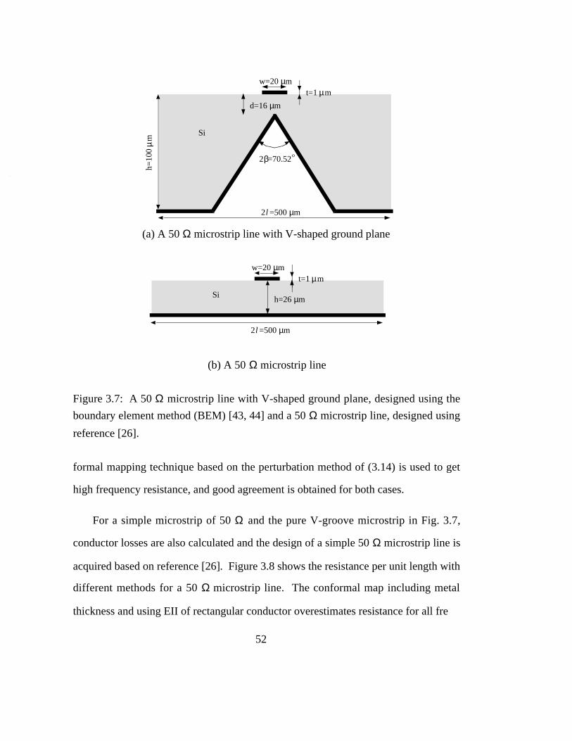
(a) A 50 Ω microstrip line with V-shaped ground plane
w=20 µm
2l =500 µm
t=1 µm
h=26 µmSi
(b) A 50 Ω microstrip line
Figure 3.7: A 50 Ω microstrip line with V-shaped ground plane, designed using the
boundary element method (BEM) [43, 44] and a 50 Ω microstrip line, designed using
reference [26].
formal mapping technique based on the perturbation method of (3.14) is used to get
high frequency resistance, and good agreement is obtained for both cases.
For a simple microstrip of 50 Ω and the pure V-groove microstrip in Fig. 3.7,
conductor losses are also calculated and the design of a simple 50 Ω microstrip line is
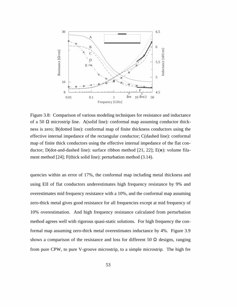
acquired based on reference [26]. Figure 3.8 shows the resistance per unit length with
different methods for a 50 Ω microstrip line. The conformal map including metal
thickness and using EII of rectangular conductor overestimates resistance for all fre
53
8
10
30
4.5
5
5.5
6
6.5
0.01 0.1 1 10 50
Indu
ctan
ce [
nH/c
m]
Frequency [GHz]
Res
ista
nce
[Ω/c
m]
δ=t δ=t/2
A
B
C
D
E
F
Figure 3.8: Comparison of various modeling techniques for resistance and inductance
of a 50 Ω microstrip line. A(solid line): conformal map assuming conductor thick-
ness is zero; B(dotted line): conformal map of finite thickness conductors using the
effective internal impedance of the rectangular conductor; C(dashed line): conformal
map of finite thick conductors using the effective internal impedance of the flat con-
ductor; D(dot-and-dashed line): surface ribbon method [21, 22]; E(8): volume fila-
ment method [24]; F(thick solid line): perturbation method (3.14).
quencies within an error of 17%, the conformal map including metal thickness and
using EII of flat conductors underestimates high frequency resistance by 9% and
overestimates mid frequency resistance with a 10%, and the conformal map assuming
zero-thick metal gives good resistance for all frequencies except at mid frequency of
10% overestimation. And high frequency resistance calculated from perturbation
method agrees well with rigorous quasi-static solutions. For high frequency the con-
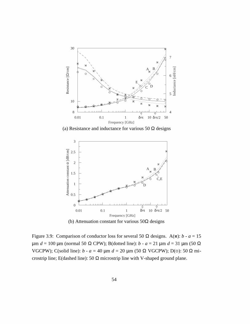
formal map assuming zero-thick metal overestimates inductance by 4%. Figure 3.9
shows a comparison of the resistance and loss for different 50 Ω designs, ranging
from pure CPW, to pure V-groove microstrip, to a simple microstrip. The high fre
54
8
10
30
4
5
6
7
0.01 0.1 1 10 50
Indu
ctan
ce [
nH/c
m]
Frequency [GHz]
Res
ista
nce
[Ω/c
m]
δ=t δ=t/2
A B
C DE
(a) Resistance and inductance for various 50 Ω designs
Atte
nuat
ion
cons
tant
α [d
B/c
m]
0
0.5
1
1.5
2
2.5
3
0.01 0.1 1 10 50Frequency [GHz]
δ=t δ=t/2
A B
D
C,E
(b) Attenuation constant for various 50Ω designs
Figure 3.9: Comparison of conductor loss for several 50 Ω designs. A(8): b - a = 15
µm d = 100 µm (normal 50 Ω CPW); B(dotted line): b - a = 21 µm d = 31 µm (50 ΩVGCPW); C(solid line): b - a = 40 µm d = 20 µm (50 Ω VGCPW); D(O): 50 Ω mi-
crostrip line; E(dashed line): 50 Ω microstrip line with V-shaped ground plane.
55
quency resistance does decrease as the V-groove gap d decreases and CPW gap (b -
a) increases, eventually approaching that of the simple microstrip line (which here is
the minimum loss configuration). For example, at 46.4 GHz the calculated attenua-
tion constant is 2.5 dB/cm for the normal CPW, falling to 2.26 dB/cm for VGCPW
with b - a = 21 µm and d = 31 µm, or 2.16 dB/cm for b - a = 40 µm and d = 20 µm;
for comparison, the calculated loss for simple 50 Ω microstrip was 2.07 dB/cm (20
µm wide and 1 µm thick strip, 26 µm high over ground plane). For constant charac-
teristic impedance designs, the VGCPW does show some reduction in loss at high
frequencies, although the rather small reduction may not justify the added complexity
of fabrication.
For the volume filament method and the surface ribbon method the impedance
matrix is first filled once (pre-process) and solved at each frequency, and for confor-
mal mapping the integration points are first searched (pre-process) and the series
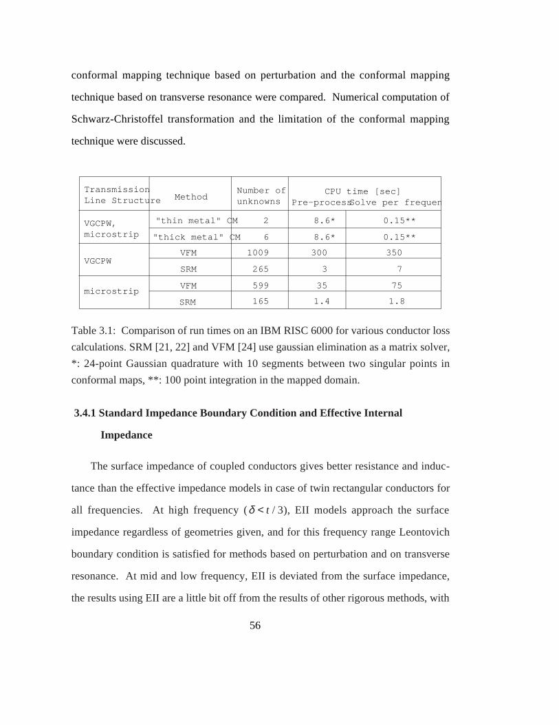
impedance is calculated easily at each frequency. Table. 3.1 compares run times and
corresponding number of unknowns on an IBM RISC 6000 for various conductor loss
calculations. This shows that conformal mapping-based models are reasonably accu-
rate as well as numerically efficient for design purposes.
3.4 Discussion and Further Consideration
The conformal mapping technique combined with EII has been shown to be very
efficient in evaluating conductor loss for quasi-TEM transmission line mode. This
method consists of two parts; first, EII is assigned on the surface of conductor, which
represents the internal behavior of the conductor. Second, the conformal map is
found for given geometries. In this section SIBC and EII were distinguished, and the
56
conformal mapping technique based on perturbation and the conformal mapping
technique based on transverse resonance were compared. Numerical computation of
Schwarz-Christoffel transformation and the limitation of the conformal mapping
technique were discussed.
TransmissionLine Structure
VGCPW,microstrip
VGCPW
microstrip
Method
"thin metal" CM
"thick metal" CM
VFM
VFM
SRM
SRM
Number ofunknowns
2
6
1009
265
599
165
CPU time [sec]Pre-processSolve per frequen
8.6*
1.4
35
3
300
8.6*
0.15**
0.15**
350
7
75
1.8
Table 3.1: Comparison of run times on an IBM RISC 6000 for various conductor loss
calculations. SRM [21, 22] and VFM [24] use gaussian elimination as a matrix solver,
*: 24-point Gaussian quadrature with 10 segments between two singular points in
conformal maps, **: 100 point integration in the mapped domain.
3.4.1 Standard Impedance Boundary Condition and Effective Internal
Impedance
The surface impedance of coupled conductors gives better resistance and induc-
tance than the effective impedance models in case of twin rectangular conductors for
all frequencies. At high frequency (δ < t / 3), EII models approach the surface
impedance regardless of geometries given, and for this frequency range Leontovich
boundary condition is satisfied for methods based on perturbation and on transverse
resonance. At mid and low frequency, EII is deviated from the surface impedance,
the results using EII are a little bit off from the results of other rigorous methods, with
57
the results using the surface impedance closer to the results of other rigorous
methods. This shows that the conformal mapping method with the EII can be used as
an approximation to the standard impedance boundary condition (SIBC). In previous
work on the perturbation method based on the conformal mapping technique, the gen-
eralized transfer impedance has been used to evaluate mid and low frequency instead
of the surface impedance of the flat conductors.
Unlike the proposed method where the varying current distribution is properly
accounted for by the transverse resonance method from uniform at DC to crowding
towards the corner and surface of the conductor at high frequency, the previous per-
turbation method based on conformal mapping technique should know the current
distribution of the conductor at low and mid frequency as well as at high frequency to
accurately evaluate the conductor loss for all frequencies. This makes it hard to
widely use the perturbation method based on conformal mapping technique.
3.4.2 Integration and Parameter Evaluation in Schwarz-Christoffel
Transformation
To numerically calculate the hyperelliptic integrals, the integration interval along
each side of the conductors is divided into 10 segments and 24-point Gaussian
quadrature is used at each interval. Gaussian procedure is good enough for many in-
tegration problems, but to compute the integral having singular points with a tolerable
accuracy a large number of points is inevitable. As explained in [45, 46], Gauss-
Chebyshev and Gauss-Jacobi quadrature formulas properly consider singular vertices
in the integral and, therefore, appear to be a good choice in the hyperelliptic integrals.
Also, much more clever partitioning of the integration interval can be derived as in
[46], where the long integration interval between singular points is divided into three
58
parts with a suitable length ratio and separate integrations are performed on those
parts with the minimal Gauss-Jacobi quadrature points. These scheme should reduce
the integration time quite a bit.
In the hyperelliptic integrals of Schwarz-Christoffel maps, the mapping coeffi-
cients should be a priori known before computing the series impedance, and various
iterative optimization schemes can be used to find the mapping coefficients. In the
study, the Powell method [46] is used, which is a direct search method and one of
least-square methods with constraints. There are many direct search methods such as
the Peckham method, the Hooke and Jeeves method, etc., and all of them can be
adopted to coefficient evaluation with some gain or loss. Gradient methods, as well as
direct search methods, can be used; for example, the steepest descent method,
Newton's method [47], Newton-Raphson Method [45], etc. Both approaches need
initial guess of the coefficients and the advantage of the gradient method over the di-
rect search method lies in accurate computation of derivatives.
3.4.3 Limits of Proposed Conformal Mapping Technique
For planar transmission lines such as a microstrip line, a coplanar strip line, a
coplanar waveguide, etc. the proposed conformal mapping technique has proven to be
quite useful in evaluating the conductor loss. But for multi-conductor (i.e., more than
two) transmission lines, a conformal map does not result in a simple parallel plate,
and, therefore, the proposed conformal mapping technique is no longer useful. As in
reference [48], planar multi-conductor transmission lines can be mapped into cylin-
drical multi-conductor lines. But even for that simplified geometry calculating self
and mutual capacitance is no longer straightforward and easy. And it necessitates a

59
more generalized technique which is still numerically efficient and accurate and is
based on more rigorous numerical method than the conformal mapping technique.