Embed Size (px)
Citation preview

8
Chapter 2
Semiconductor Laser OpticalPhase-Locked Loops
2.1 OPLL Basics
The SCL-OPLL, shown in figure 2.1, is a feedback system that enables electronic
control of the phase of the output of an SCL. The fields of the master laser and the
slave SCL are mixed in a photodetector PD. A part of the detected photocurrent is
monitored using an electronic spectrum analyzer. The detected output is amplified,
mixed down with an “offset” radio frequency (RF) signal, filtered and fed back to the
SCL to complete the loop.
A schematic model of the OPLL is shown in figure 2.2(a). We will assume that the
free-running SCL has an output as cos(
ωfrs t+ φfr
s (t))
, where the “phase noise” φfrs (t)
is assumed to have zero mean. When the loop is in lock, we drop the superscript fr
from the laser phase and frequency variables. Similarly, the master laser output is
given by am cos (ωmt+ φm(t)). The detected photocurrent is then
iPD(t) = ρ(
a2m + a2s + 2asam cos [(ωm − ωs) t+ (φm(t)− φs(t))])
, (2.1)
where ρ is the responsivity of the PD. The last term above shows that the PD
acts as a frequency mixer in the OPLL. Let us further define a photodetector gain
KPD.= 2ρ 〈asam〉, where 〈.〉 denotes the average value. The detected photocurrent
is then mixed down with a radio frequency (RF) signal, whose output is taken to

9
������������������������������������������������������������������������������������������������������������������������������������������������������������������������������������������������������������������������������������������������������������������������������������������������������������������������������������������������������������������������������������������������������������������������������������������������������������������������������������������������������������������������������������������������������������������������������������������������������������������������������������������������������������������������������������������������������������������������������������������������������������������������������������������������������������������������������������������������������������������������������������������������������������������������������������������������������������������������������������������������������������������������������������������������������������������������������������������������������������������������������������������������������������������������������������������������������������������������������������������������������������������������������������������������������������������������������������������������������������������������������������������������������������������������������������������������������������������������������������������������������������������������������������������������������������������������������������������������
Semiconductor
Laser
������������������������������������������������������������������������������������������������������������������������������������������������������������������������������������������������������������������������������������������������������������������������������������������������������������������������������������������������������������
PD
Gain
������������������������������������������������������������������������������������������������������������������������������������������������������������������������������������������������������������������������������������������������������������������������������������������������������������������������������������������������������������Filter
����������������������������������������������������������������������������������������������������������������������������������������������������������������������������������������������������������������������������������������������������������������������������������������������������������������������������������������������������������������������������������������������������������������������������������������������������������������������������������������������������������������������������������������������������������������������������������������������������������������������������������������������������������������������������������������������������������������
RF Offset
����������������������������������������������������������������������������������������������������������������������������������������������������������������������������������������������������������������������������������������������������������������������������������������������������������������������������������������������������������������������������������������������������������������������������������������������������������������������������������������������������������������������������������������������������������������������������������������������������������������������������������������������������������������������������������������������������������������������������������������������������������������������������������������������������������������������������������������������������������������������������������������������������������������������������������������������������������������������������������������������������������������������������������������������������������������������������������������������������������������������������������������������������������������������������������������������������������������������������������������������������������������������������������������������������������������������������������������������������������������������������������������������������������������������������������������������������������������
Master Laser
(Fiber Laser)
����������������������������������������������������������������������������������������������������������������������������������������������������������������������������������������������������������������������������������������������������������������������������������������������������������������������������������������������������������������������������������������������������������������������������������������������������������������������������������������������������������������������������������������������������������������������������������������������������������������������������������������������������������������������������������������������������������������������������������������������������������������������������������������������������������������������������������������������������������������������������������������������������������������������������������������������������������������������������������������������������������������������������������������������������������������������������������������������������������������������������������������������������������������������������������������������������������������������������������������������������������
Spectrum
Analyzer
Figure 2.1. A heterodyne semiconductor laser optical phase-locked loop. PD: photo-detector.
be aRF sin (ωRF t + φRF (t)). The choice of trigonometric functions ensures a mixer
output of the form
iM(t) = ±KMKPDaRF sin [(ωm − ωs ± ωRF ) t + (φm(t)− φs(t)± φRF (t))] . (2.2)
Without loss of generality, we will consider only the “+” sign in the rest of this thesis.
This mixer output is amplified with gain Kamp, filtered and fed into the SCL, which
acts as a current-controlled oscillator whose frequency shift is proportional to the
input current, i.e.,
δωs = −Ksis(t) = −KsKampiM(t) (2.3)
The minus sign indicates that the frequency of the SCL decreases with increasing
current. A propagation delay τL is included in the analysis. We will assume that the
filter has a unity gain at DC, i.e., the area under its impulse response is zero. We
lump together the DC gains of the various elements in the loop, and denote it by Kdc,
i.e., Kdc = aRFKMKPDKampKs. This parameter will shortly be defined in a more
rigorous manner. When in lock, the frequency shift of the SCL is given by
δωs = −Kdc sin [(ωm − ωs ± ωRF ) t+ (φm(t)− φs(t)± φRF (t))] . (2.4)

10
LoopFilter
Master Laser
Laser Phase-Lockedto Master
LocalOscillator (LO) SCL
ωst + φs
ωmt + φm
Phase Error
ωRF t + φRF
RF Offset
φe
Mixer
Photodetector
τLDelay
Gain
Kdc
(a)
φfrs (s)
PD
Ff(s)
φs(s)
Gain Kdc cos (φe0)
Kdc sin (φe0) r(s)/2
Delay
FilterSCL
e−sτL
FFM(s)× 1/s
φm(s) + φRF (s)
(b)
Figure 2.2. (a) Schematic diagram of an OPLL. (b) Linearized small-signal model forphase noise propagation in the OPLL.
The frequency of the slave laser is the sum of the free-running frequency and the
correction from the feedback loop, i.e.,
ωs = ωfrs + δωs. (2.5)
The free-running frequency difference between the slave and master lasers (offset
by the RF frequency) is defined as
∆ωfr.= ωm − ωfr
s + ωRF . (2.6)
We now derive the the steady-state operating point of this laser [2]. In steady state,
the error signal at the output of the mixer (equation (2.2)) does not change with

11
time, which yields
ωs = ωm + ωRF ,
φ̄s = φ̄m + φ̄RF + φe0.(2.7)
The bars in the second part of equation (2.7) denote that this equation is valid for the
steady-state values of the phase. The parameter φe0 is the steady-state phase error in
the loop. This phase error is a consequence of the feedback current keeping the loop
in lock, which can be understood by substituting equation (2.7) into equation (2.4)
and using equations (2.5) and (2.6) to obtain
δωs = ∆ωfr = Kdc sinφe0. (2.8)
The frequency shift induced by the feedback loop, δωs, compensates for the free-
running frequency difference between the slave and master lasers, and its maximum
value is limited by the DC gain of the loop. The maximum value of the free-running
frequency difference that the loop can tolerate in lock is called the “hold-in range,”
and is defined in section 2.1.2. The steady-state phase error is given by
φe0 = sin−1
(
∆ωfr
Kdc
)
. (2.9)
It is important that the DC gain Kdc be as large as possible and the laser free-running
frequency fluctuations be minimized, so that φe0 is small. Indeed, this is the case in
most well-designed OPLLs, and we will ignore this steady state phase error in large
parts of this thesis. In the absence of φe0, the phase of the locked slave SCL exactly
follows that of the master laser, offset by the RF phase.
The heterodyne OPLL of figure 2.1 differs from the homodyne PLL shown in
figure 1.1 in the addition of an extra reference (“offset”) RF oscillator. This results
in some powerful advantages: as is clear from equation (2.7), the optical phase can be
controlled in a degree for degree manner by adjusting the electronic phase of the offset
signal. Further, heterodyne locking ensures that the beat note at the photodetector
is at an intermediate frequency, where it is away from low-frequency noise sources

12
and can easily be separated from the low frequency (“DC”) terms.
2.1.1 Small-Signal Analysis
The OPLL is next linearized about the steady-state operating point given in equation
(2.7) and the propagation of the phase around the loop is analyzed in the Laplace
domain [2], as shown in figure 2.2(b). The variables in the loop are the Laplace
transforms of the phases of the lasers and the RF signal.1 Fourier transforms are also
useful to understand some loop properties, and will be used in parts of the thesis. The
Fourier transform X(f) is the Laplace transform X(s) evaluated along the imaginary
axis, s = j2πf . The notation X(ω) is also used in literature to denote the Fourier
transform, with the angular Fourier frequency, ω, given by ω = 2πf ; we will use X(f)
in this thesis to avoid confusion. It is to be understood that the steady-state values
of the phase in equation (2.7) are subtracted from the phases before the Laplace
(or Fourier) transform is computed. The free-running phase fluctuation of the slave
SCL (“phase noise”) is denoted by the additive term φfrs (s).2 The summed relative
intensity noises of the lasers r(s) are also incorporated into the model.3
The SCL acts as a current-controlled oscillator and, in the ideal case, produces
an output phase equal to the integral of the input current for all modulation fre-
quencies, i.e. it has a transfer function 1/s. However, the response of a practical
SCL is not ideal, and the change in output optical frequency is a function of the
frequency components of the input current modulation. This dependence is modeled
by a frequency-dependent FM response FFM(s). The shape of the FM response and
1Notation: the Laplace transform of the variable x(t) is denoted by X(s). For Greek letters, theFourier transform of φ(t) is just denoted by φ(s). The argument s is sometimes dropped when theusage is clear from the context.
2Strictly speaking, the Laplace or Fourier transform of the phase noise cannot be defined—itis a random process, and we can only describe its spectral density. However, the use of Laplacetransforms provides valuable insight—for this purpose, we can regard the observed phase noise asa particular instance of the underlying random process. The spectral density will be used in allcalculations involving the phase noise, e.g., see chapter 3.
3The model of figure 2.2(b) is easily derived by noting that the expansion of the phase detec-tor output Kdc (1 + r(t)/2) sin (φe0 + φe(t)) about the steady state value Kdc sinφe0 is Kdc sinφe0
+ (Kdc sinφe0) r(t)/2 + (Kdc cosφe0)φe(t). The relative amplitude noise is one-half the relativeintensity noise.

13
its effects are discussed in section 2.3. The filter response and the FM response of
the SCL are assumed to be normalized to have unit gain at DC, i.e., Ff (0) = 1,4
FFM(0) = 1. For simplicity, we have also assumed that the photodetector and mixer
have flat frequency responses—this is true if wideband detectors and mixers are used
in the loop, as is the case in this work. It is straightforward to include nonuniform
detector and mixer responses in the analysis.
Let us define the open-loop transfer function of the loop as the product of the
transfer functions of all the elements in the loop for the ideal case φe0 = 0:
Gop(s) =KdcFf(s)FFM(s)e−sτL
s. (2.10)
This allows us to define the DC gain in a more rigorous manner:
Kdc.= lim
s→0sGop(s). (2.11)
The phase of the locked SCL is then given by
φs(s) = (φm(s) + φRF (s))Gop cosφe0
1 +Gop cosφe0
+φfrs (s)
1 +Gop cosφe0
+r(s)
2
Gop sin φe0
1 +Gop cos φe0
,
(2.12)
where we have omitted the argument s in Gop(s). Phase noise, φfrs (s), represents
the largest source of noise in an SCL-OPLL due to the relatively large linewidth of
an SCL, and the contribution of the last term on the right-hand side can usually be
neglected, especially if φe0 ≈ 0. We will therefore ignore the laser relative intensity
noise in the rest of this thesis. For similar reasons, we also neglect the effects of
shot noise and detector noise on the phase of the SCL in this thesis. It will also be
assumed, unless stated otherwise, that φe0 = 0.
4For some filter transfer functions, e.g., integrators, this normalization is not feasible. In suchcases, we simply let Kdc → ∞.

14
2.1.2 OPLL Performance Metrics
We now define the important OPLL performance metrics that will be used in this
work.
Loop bandwidth is the largest Fourier frequency for which the open loop transfer
function Gop(f) is larger than unity. From equation (2.12), this means that the
phase of the locked SCL follows that of the master and the RF offset within the
loop bandwidth, and reverts to the free-running value at higher frequencies. The
loop bandwidth is usually limited by the stability of the loop—in particular,
we will use the Bode stability criterion [2], which states that the magnitude
of the complex valued function Gop(f) should be lesser than unity when its
phase is lesser than or equal to −π. The frequency at which the phase response
equals −π is referred to as the “phase-crossover frequency” and represents the
maximum possible value of the loop bandwidth.
Hold-in range is defined as the largest change in the free-running frequency of the
slave SCL over which the loop still remains in lock. This can be evaluated from
equation (2.8), where the sine function takes a maximum value of unity. Using
equation (2.11), we write the hold-in range as
fhold =1
2πlims→0
sGop(s). (2.13)
Clearly, a large hold-in range is desired so that the loop is insensitive to envi-
ronmental fluctuations.
Residual phase error in the loop is one of the most important metrics to evaluate
the performance of the loop. It is defined as the variance in the deviation of the
phase of the locked SCL from the ideal case where it follows the master laser,
i.e.,
σ2φ =
⟨
(φs(t)− φm(t)− φRF (t))2⟩
, (2.14)

15
where 〈.〉 denotes averaging over all time.5 Using the Wiener-Khintchine theo-
rem, equation (2.14) can be written in the frequency domain as
σ2φ =
∫
∞
−∞
Seφ(f) df, (2.15)
where Seφ(f) is the spectral density of the random variable φs(t)−φm(t)−φRF (t),
i.e., the spectrum of the phase error. Using equation (2.12), and assuming
φe0 = 0, we have
Seφ(f) =
∣
∣
∣
∣
1
1 +Gop(f)
∣
∣
∣
∣
2(
Smφ (f) + Ss,fr
φ (f))
, (2.16)
where we have used the fact that the phase noise of the master laser and free-
running slave laser are uncorrelated. Smφ (f) and Ss,fr
φ (f) are the spectra of the
phase noise of the master and free-running slave SCL respectively, and the phase
noise of the RF source is assumed to be negligible. Under the assumption of a
Lorenzian lineshape for the lasers, these spectral densities are related to their
3 dB linewidths ∆ν by [72]
Smφ (f) =
∆νm2πf 2
,
Ss,frφ (f) =
∆νs2πf 2
.(2.17)
Using (2.16) and (2.17) in (2.15), we obtain the result for the variance of the
residual phase error of the OPLL:
σ2φ =
∆νm +∆νs2π
∫
∞
−∞
1
f 2
∣
∣
∣
∣
1
1 +Gop(f)
∣
∣
∣
∣
2
df. (2.18)
For a stable OPLL, we require that σ2φ ≪ 1 rad2. σφ is the standard deviation
of the residual phase error, measured in radians.
Settling time is defined as the time taken by the error signal in the loop to relax
back to its steady-state value, within 1%, when a step phase input ∆φ is applied.
5For simplicity, we make the common assumption that the phase noise is a stationary process.

16
Open-loop
transfer function
Gop(f)
φm(f)
φs(f)
PD
φfrs (f)
Figure 2.3. Simplified schematic diagram of an OPLL.
If the step is applied at t = 0, the phase error goes from (φe0 +∆φ) to (φe0 +
0.01∆φ) at time t = τs. Alternatively, this is the time taken by the laser phase
to change by 0.99∆φ. The settling time is of interest in applications where the
laser phase is changed using an RF phase input.
The response of the loop error signal to a step input is given by
φe(t)− φe0 = L−1
[
∆φ1
s (1 +Gop(s))
]
, (2.19)
where L−1 is the inverse Laplace transform operator.
Other OPLL metrics such as acquisition range, mean time between cycle-slips etc.
are not central to this work and will not be considered here. Some of these metrics
are discussed in references [2, 73].
2.2 Performance of Different OPLL Architectures
We now evaluate the performance metrics listed above for three different OPLL ar-
chitectures that are relevant to this work. In this section, we assume that the FM
response of the SCL is flat, i.e., FFM(f) = 1. The “type” of an OPLL is the number
of poles6 at s = 0, and its “order” is the total number of poles. The RF source is
assumed to have no noise, which allows the OPLL to be simplified as in figure 2.3.
6A pole is a root of the equation D(s) = 0, where D(s) is the denominator of the open-looptransfer function Gop(s).

17
As a concrete example, let us assume that the summed linewidth of the master and
slave lasers is 0.5 MHz, which is representative of (good) DFB SCLs.
2.2.1 Type I OPLL
This OPLL has a transfer function
Gop(f) =K
j2πf, (2.20)
where the pole at f = 0 denotes that the optical phase at the output of the SCL is
obtained by integrating the input control signal. The magnitude and phase of Gop(f)
are plotted in a “Bode plot” in figure 2.4(a). Since the phase of Gop(f) never goes to
−π, this OPLL is unconditionally stable, with bandwidth and hold-in range K/2π.
Practical OPLLs are always bandwidth-limited; let us therefore arbitrarily assume
that the bandwidth of this loop is 2 MHz, i.e., K = 1.26× 10⁷ rad/s.
The laser frequency drifts due to fluctuations in the laser bias current and tem-
perature. Assuming that a low noise current source is used to bias the laser, the
primary source of free-running frequency variations is environmental temperature
fluctuations. The thermal frequency tuning coefficient of InP-based lasers is typically
10 GHz/◦C. A hold-in range of 2 MHz therefore means that the loop loses lock if the
SCL temperature fluctuates by only ∼ 2× 10⁻⁴ ◦C.
The residual phase error of this loop is given by
σ2φ =
π(∆νm +∆νs)
K, (2.21)
which, with the assumed values of laser linewidth and loop bandwidth, yields σ2φ =
0.4 rad2. Equation (2.21) leads us to an important general result: it is necessary that
the summed linewidths of the two lasers be much smaller than the loop bandwidth for
good OPLL performance.

18
100
105
1010
−200
0
200
Frequency (Hz) →
Magnitude (
dB
) →
Bode Plot
100
105
1010
−180
−90
0
Frequency (Hz) →
Phase (
degre
es) →
(a)
100
105
1010
−200
0
200
Frequency (Hz) →
Magnitude (
dB
) →
Bode Plot
100
105
1010
−360
−270
−180
−90
0
Frequency (Hz) →
Phase (
degre
es) →
(b)
Figure 2.4. Bode plots for (a) a Type I OPLL and (b) a Type I OPLL with apropagation delay of 10 ns. The phase-crossover frequency is indicated by the markerin (b).

19
The response of the phase error to a step response is
φe(t)− φe0 = ∆φ exp(−Kt), (2.22)
which gives a 99% settling time of τs ≃ 4.6/K ≃ 4× 10⁻⁷ s.
The high sensitivity of this loop to temperature fluctuations is due to the arbitrary
bandwidth limit assumed; however other factors such as the SCL FM response and
loop propagation delay, discussed later, do impose such a restriction. It is therefore
important to design loop filters to increase the DC gain and loop bandwidth.
2.2.2 Type I, Second-Order OPLL
The extremely high sensitivity of the basic Type I OPLL to temperature fluctuations
can be overcome using a filter Ff (f) = (1 + j2πfτ0)/(1 + j2πfτ1), with τ0 < τ1.
This filter is called a lag filter or lag compensator [74]7 since its response has a phase
lag (phase response is <0). The value of τ0 is chosen so that τ−10 is much smaller
than the loop bandwidth, which ensures that the filter response does not affect the
phase-crossover frequency. To maintain the same value of the loop bandwidth as the
Type I OPLL, the loop gain has to be increased by a factor τ1/τ0, so that the loop
transfer function is
Gop(f) =K
j2πf×
τ1τ0
×1 + j2πfτ01 + j2πfτ1
. (2.23)
In the limit of τ1 → ∞, this loop is a Type-II control system.
The bandwidth of this loop isK/2π = 2 MHz, while the hold-in range isKτ1/2πτ0.
By proper choice of τ1 and τ0, a hold-in range of several gigahertz can be achieved. A
hold-in range of 1 GHz corresponds to a temperature change of 0.1 ◦C, and the SCL
temperature is easily controlled to much smaller than this value.
The addition of the lag filter at low frequencies does not affect the residual phase
error σ2φ, since most of the contribution to the integral in equation (2.18) is from
frequencies of the order of the loop bandwidth.
7Some authors, e.g., [2], refer to this filter as a lag-lead filter.

20
MasterLaser
SlaveLaser
Gain
K
sφ
mφ
eφ
RFφ
RF Phase
+- +
+
1
11
K
sτ+
+
+
Figure 2.5. Type I, second-order OPLL using an active filter.
When a step input ∆φ is applied, the phase error in the loop varies as
φe(t)− φe0 = L−1
(
∆φs+ 1/τ1
s2 + s( 1τ1+K) + K
τ0
)
. (2.24)
Using the approximation τ−10 ≪ τ−1
1 ≪ K, this is an overdamped system, and the
final solution for the phase error transient is
φe(t)− φe0 = ∆φ exp(−Kt), (2.25)
which is identical to the simple Type I OPLL. The settling time of the loop is therefore
unaffected, and the OPLL settles to (99% of) the new set-point in a time τs ≃ 4.6/K =
4× 10⁻⁷ s.
The loop filter described above is easily realized using passive R-C circuits [66].
The drawback of a passive filter is that additional gain has to be provided by the
amplifier in the loop, which is not always feasible due to amplifier saturation. This
can be overcome using an active low-pass filter in a parallel arm [66] as shown in figure
2.5. The additional branch has high DC gain (K1 ≫ K), and the pole is located at
low frequencies so that it does not affect the loop bandwidth (K1/Kτ1 ≪ 1). The

21
transfer function of this loop is
Gop(f) =1
j2πf
(
K +K1
1 + j2πfτ1
)
, (2.26)
which is identical to equation (2.23) with τ0/τ1 = K/K1.
2.2.3 Type I OPLL with Delay
We now study an OPLL in the presence of propagation delay. It must be empha-
sized that all negative feedback systems suffer from delay limitations, but the wide
linewidth of SCLs makes the delay a very important factor in OPLLs, and has been
studied by different authors [75,76]. The transfer function of a delay element is given
by exp(−j2πfτL) where τL is the delay time. We write the open loop transfer function
of a first-order loop with delay τL as
G(f) =KL
jfexp(−j2πfτL)
=K̄L
jf̄exp
(
−j2πf̄)
, (2.27)
where the normalized variables are defined as
f̄.= fτL,
K̄L.= KLτL. (2.28)
We identify the π-crossover frequency and the maximum stable gain by ∠G(fπ) =
−π and |G(fπ)| = 1:
f̄π = 1/4 ,
K̄L,max = 1/4 . (2.29)
The loop bandwidth is therefore limited to 1/(4τL), which is equal to the maximum
hold-in range. The Bode plot for this transfer function is calculated and plotted

22
0 0.05 0.1 0.15 0.2 0.250
50
100
150
Normalised Loop gain KL τ
L →
σφ2 /
(∆
ν m
+ ∆
ν s
) τ L
(ra
d2) →
Figure 2.6. Variation of the minimum variance of the phase error as a function of thenormalized gain for a Type I OPLL in the presence of propagation delay.
in figure 2.4(b), assuming a delay τL = 10 ns, which is a typical value for optical
fiber-based OPLLs. The phase crossover frequency is then equal to 25 MHz.
The variance of the residual phase error is calculated using equation (2.27) in
equation (2.18) to obtain
σ2φ = τL
∆νm +∆νs2π
∫
∞
−∞
df̄
K̄2L + f̄ 2 − 2K̄Lf̄ sin(2πf̄)
. (2.30)
The calculated value of the variance of the phase error as a function of the nor-
malized gain is shown in figure 2.6. As expected, the phase error is very large at
K̄L = 0 (no PLL correction) and K̄L = 1/4 (borderline instability). The phase error
is minimum when K̄L = K̄L,opt = 0.118, and the minimum value is given by
σ2φ,min = 9.62 τL(∆νm +∆νs). (2.31)
For a delay of 10 ns, the minimum achievable phase error is 0.05 rad2.

23
2.2.4 Type II Loop with Delay
The limited hold-in range of the Type I loop of the previous loop can be improved
using a lag filter design similar to section 2.2.2. Here, we consider the limiting case
(τ1 → ∞) of a Type II OPLL. In the presence of a propagation delay τL, the open
loop transfer function is given by
G(f) = −KL(1 + j2πfτ0)
f 2exp(−j2πfτL)
= −K̄L(1 + j2πf̄ τ̄0)
f̄ 2exp
(
−j2πf̄)
, (2.32)
where the normalized variables are defined as
f̄.= fτL,
K̄L.= KLτ
2L,
τ̄0.= τ0/τL. (2.33)
The π-crossover frequency is identified by setting ∠G(fπ) = −π, to obtain
tan(2πf̄π) = 2πf̄πτ̄0. (2.34)
A solution to this equation exists only if τ̄0 > 1, or τ0 > τL. In other words, the loop
is stable only if, at low frequencies, the phase lead introduced by the zero is larger
than the phase lag introduced by the delay. The maximum stable loop gain is given
by
K̄L,max =f̄ 2π
√
1 + (2πf̄πτ̄0)2. (2.35)
The variation of f̄π and K̄L,max as a function of the position of the loop zero τ̄0
are plotted in figure 2.7, from which it is clear that the loop bandwidth approaches
the limit 1/(4τL) as τ̄0 increases. The hold-in range of this loop is infinite, owing to
the presence of the pole at f = 0.
We next calculate the variance of the residual phase error by plugging equation

24
100
101
102
103
0.1
0.15
0.2
0.25
0.3
τ0/τ
L →
f π τ
L →
100
101
102
103
0
0.005
0.01
0.015
τ0/τ
L →
KL,m
ax τ
2 L →
(a)
(b)
Figure 2.7. Variation of (a) the π-crossover frequency f̄π and (b) the maximum stableloop gain K̄L,max as a function of the position of the loop zero τ̄0, for a Type II OPLLin the presence of a delay τL.
(2.32) into equation (2.18) to obtain
σ2φ = τL
∆νm +∆νs2π
×
∫
∞
−∞
f̄ 2 df̄
K̄2L + f̄ 4 + 4π2K̄2
Lτ̄21 f̄
2 − 2K̄Lf̄ 2 cos(2πf̄)− 4πK̄Lτ̄0f̄ 3 sin(2πf̄),
(2.36)
which is a function of both τ̄0 and K̄L. As seen in the previous section, for a given
value of τ̄0, there is an optimum value of K̄L that minimizes the variance of the phase
error. For this OPLL architecture, the optimum gain is related to the maximum
stable loop gain byKL,opt
KL,max
= 0.47 . (2.37)
The value of the minimum of the variance of the phase error as a function of τ̄0 is
shown in figure 2.8. As τ̄0 is increased, the minimum variance of the phase error

25
100
101
102
103
0
20
40
60
80
100
120
τ0/τ
L →
σ2 m
in / (∆
ν m
+ ∆
ν s
) τ L
(ra
d2) →
Figure 2.8. Variation of the minimum variance of the phase error as a function of theparameter τ̄0, for a Type II OPLL with delay τL.
asymptotically reaches the value
limτ̄0→∞
σ2min = 9.62 τL(∆νm +∆νs). (2.38)
This result is identical to the result obtained for a first-order loop with delay in (2.31).
We therefore arrive at the conclusion that in the presence of propagation delay, the
performance of a second-order loop is not superior to that of a first-order loop in
terms of the residual phase error. The advantage is the increased hold-in range which
makes the loop insensitive to environmental fluctuations.
The settling time of OPLLs with propagation delay cannot be calculated in closed
form, but is of the order of the propagation delay in the loop. It is important to
minimize the loop delay in order to reduce the variance of the phase error and the
settling time, and OPLLs constructed using microoptics [20] and recent efforts toward
integrated OPLLs [22, 23, 77] are steps toward high-performance OPLL systems.

26
104
105
106
107
108
0.2
0.4
0.6
0.8
1
1.2
Frequency (Hz) →
Magnitude (
dB
) →
Experiment
Fit
104
105
106
107
108
−180
−135
−90
−45
0
Frequency (Hz) →
Phase (
degre
es) →
Experiment
Fit
Figure 2.9. Experimentally measured FM response of a commercial DFB laser (JDS-Uniphase) with a theoretical fit using a low-pass filter model [32].

27
2.3 FM Response of Single-Section SCLs
We have shown that the loop propagation delay ultimately limits the achievable
bandwidth and residual phase error in an OPLL, and reducing the delay is ultimately
very important to achieve high-speed OPLLs. However, this discussion ignored the
nonuniform frequency modulation response of the slave SCL. In practice, the biggest
challenge in constructing stable OPLLs is not the propagation delay, but the SCL FM
response, which limits the achievable bandwidth. The FM response of single-section
SCLs is characterized by a thermal redshift with increasing current at low modulation
frequencies, and an electronic blueshift at higher frequencies. This implies that at
low modulation frequencies, the variation of the output optical frequency is out of
phase with the input modulation, whereas the optical frequency changes in phase with
the input modulation at high modulation frequencies. The FM response of the SCL
therefore has a “phase reversal,” which occurs at a Fourier frequency in the range of
0.1–10 MHz.
Different theoretical models have been used in literature to explain the thermal
FM response of a single section SCL, including an empirical low-pass filter (LPF)
response [32] and a more “physical” model based on the dynamics of heat transfer
within the laser [78], [79]. In this work, we will use the empirical LPF model since it
better fits the experimentally measured response of various DFB lasers, an example of
which is shown in figure 2.9 for a commercially available DFB laser (JDS-Uniphase)
at a wavelength of 1539 nm. The SCL FM response was measured by modulating the
laser with a sinusoidal modulating current and using a Mach-Zehnder interferometer
(MZI) biased in quadrature as a frequency discriminator [80]. The measurement
system is calibrated using the amplitude modulation response as the baseline.
The LPF model for the FM response takes the form
FFM(f) = Kel −Kth
1 +√
jf/fc, (2.39)
where the first term denotes the broadband electronic response and the second term

28
denotes the thermal response. Note the opposite signs of the two effects—this implies
that the phase of the FM response goes through a change of π radians (a “phase-
reversal”) as shown in figure 2.9. It is also important to note that this is a relatively
“low-frequency” behavior, as opposed to high-speed free-carrier effects near the relax-
ation resonance frequency which have been studied more extensively [81,82]. Equation
(2.39) can be rewritten in the form
FFM(f) =1
b
(
b−√
jf/fc
1 +√
jf/fc
)
, (2.40)
where fc denotes the corner frequency of the thermal response and depends on the
device material and structure, and b = Kth/Kel − 1 denotes the relative strength of
the thermal and electronic responses. For typical SCLs, b > 0, and fc lies in the
range of 0.1–10 MHz. The fit to the experimental data in figure 2.9 was obtained
with b = 1.64 and fc = 1.8 MHz.8 A similar phase reversal was measured in a variety
of single-section SCLs characterized in our lab. We will only consider b > 0 in this
analysis, since it is the most typical case. If b < 0, the electronic response always
dominates, and there is no phase reversal.
2.4 OPLL Filter Design
When the FM response of the SCL is included, the open-loop transfer function takes
the form
Gop(f) =K
j2πf
1
b
(
b−√
jf/fc
1 +√
jf/fc
)
, (2.41)
whose Bode plot is shown in figure 2.10(a) for the fitting parameters b = 1.64 and
fc = 1.8 MHz. It is clear that the FM response severely limits the phase-crossover
frequency, limiting the loop bandwidth and increasing the residual phase error. This
FM response limitation justifies the omission of the propagation delay in the above
8The fit is not very sensitive to the parameters b and fc, and allowing for errors in experimentalmeasurement, reasonably good fits are obtained for b in the range 1.5 to 3 and fc between 0.7 and2 MHz. In section 2.7, we use the values b = 2.7 and fc = 2.76 MHz and the two curves are virtuallyindistinguishable.

29
equation; in fact, it is not possible to achieve delay-limited performance with single-
section SCLs in standard OPLLs. For these fitting parameters, the minimum variance
of the residual phase error can be calculated to be equal to (see appendix A)
σ2min = 8× 10⁻⁷ (∆νm +∆νs) , (2.42)
which yields a value of 0.4 rad2 for a summed linewidth of 0.5 MHz.
The effect of the FM response can be somewhat mitigated using loop filters. We
have developed a number of techniques to improve loop performance, and these are
described in detail in reference [73]. We will here describe the salient features of our
filter design. Firstly, a lead filter is used to push the phase-crossover frequency to
higher frequencies, as shown in the Bode plot in figure 2.10(b). Such a filter has the
form
Ff(f) =1 + j2πfτ21 + j2πfτ3
, (2.43)
with τ2 > τ3, and the values τ2 = 10−7s and τ3 = 10−9s were used in the calculation.
The use of the lead filter reduces the minimum variance of the phase error from ∼0.4
to ∼0.2 rad2. This value is in reasonable agreement with the experimentally measured
residual phase error of 0.12 rad2 for an optimized OPLL with this SCL (see section
2.5).9
An OPLL using a single-section SCL therefore requires that the SCL linewidth
should be very narrow (<1 MHz), and a lead filter is necessary to improve the loop
bandwidth. The hold-in range of the OPLL is still limited by the low DC gain of
a Type I OPLL, and we therefore add a lag filter at low frequencies to increase the
hold-in range, as analyzed in section 2.2.2. A practical SCL-OPLL configuration
is therefore described in figure 2.11, and we have experimentally demonstrated an
increase in the hold-in range from ∼10 MHz to ∼3.5 GHz using this configuration.
9An important cause of the discrepancy between theory and experiment is the assumption ofa Lorenzian lineshape for the laser—it is shown in chapter 3 that this slave SCL has a significantamount of 1/f noise at low frequencies, which contributes to the measured free-running linewidth,but is very well corrected by the OPLL leading to a smaller residual phase error.

30
100
105
1010
−200
0
200
Frequency (Hz) →
Magnitude (
dB
) →
Bode Plot
100
105
1010
−270
−180
−90
0
Frequency (Hz) →
Phase (
degre
es) →
(a)
100
105
1010
−200
0
200
Frequency (Hz) →
Magnitude (
dB
) →
Bode Plot
100
105
1010
−270
−180
−90
0
Frequency (Hz) →
Phase (
degre
es) →
(b)
Figure 2.10. Bode plots for (a) a Type I OPLL including the SCL FM response,and (b) the same response with an additional lead filter. The lead filter pushes thephase-crossover frequency (indicated by the marker) to higher frequencies, enablinga larger loop bandwidth.

31
MasterLaser
SlaveLaser
Gain
K
RF Phase
+- +
+
1
11
K
sτ+
+
+
2
3
1
1
s
s
τ
τ
+
+
sφ
mφ
eφ
RFφ
Figure 2.11. Practical OPLL configuration, including a lead filter to increase thephase-crossover frequency and a low frequency active lag filter (implemented by theparallel arm) to increase the hold-in range.
2.5 Phase-Locking of Commercial SCLs
We phase-locked a number of commercially available SCLs of different types and
operating wavelengths in the heterodyne OPLL configuration shown in figure 2.1.
We present phase-locking results of five different SCLs in table 2.1: a DFB laser at
1539 nm (JDS-Uniphase Corp., Milpitas, CA), an external cavity SCL at 1064 nm (In-
novative Photonic Solutions, Monmouth Junction, NJ), a high power master-oscillator
power amplifier (MOPA) SCL at 1548 nm (QPC Lasers, Sylmar, CA), a vertical ex-
ternal cavity surface-emitting laser (VECSEL) at 1040 nm (Novalux, Sunnyvale, CA,
with a home-built external cavity) and a DFB laser at 1310 nm (Archcom Tech.,
Azusa, CA). The temperature of the slave SCLs was controlled to within 0.01 ◦C
using a thermoelectric cooler. Different master lasers were used in the experiments.
The outputs of the fiber-coupled slave and master lasers were combined using a fiber
coupler, and a high speed PD (NewFocus 1544-B) was used to detect the beat note
between the lasers. A tunable RF oscillator with linewidth ≪ 10 kHz was used as

32
Table 2.1. Parameters of OPLLs demonstrated using commercially avail-able SCLs
Slave λ SCL SCL 3 dB Master σ2φ
SCL (nm) power linewidth Laser (rad2)
DFBa 1539 60 mW 0.5 MHz Fiber Laserh 0.11
Ext. cavityb 1064 100 mW 0.2 MHz Fiber Laserh 0.014
MOPAc 1548 1000 mW 0.5 MHz Tunable Laseri 0.08
VECSELd 1040 40 mW <0.01 MHzf VECSELd 0.007
DFBe 1310 5 mW ∼0.5 MHzg DFB SCLe 0.2
a JDS-Uniphase Corp.b Innovative Photonic Solutions.c QPC Lasers.d Novalux, with home-built cavity.e Archcom Tech.f This is an estimate, the actual linewidth was too low to be measuredby the self-heterodyne technique.
g Measured by beating two similar DFB lasers.h NP Photonics, Tucson, AZ, linewidth ∼30 kHz.i Agilent, linewidth ∼50 kHz.
the offset signal. Discrete RF amplifiers and mixers (MiniCircuits, Brooklyn, NY)
were used to provide gain and mix the RF signals. The DC current and the temper-
ature of the slave SCL were adjusted to bring the free-running frequency difference
between the master and slave SCLs to within the loop acquisition range. The total
propagation delay in the loop was estimated to be of the order of 10 ns. Filters were
used to increase the loop hold-in range and bandwidth as described in the previous
section, and stable phase-locking for at least 30 minutes was observed.
The phase-locking performance was characterized by measuring a part of the loop
PD output using a high speed spectrum analyzer, and the results are shown in figure
2.12. The offset RF frequency, which ranged from 0.8 to 1.7 GHz in these experiments,
is subtracted from the x-axis. If the phase-locking is perfect, this signal is a pure tone
at the frequency ωs−ωm = ωRF (zero in the figure). However, imperfect phase-locking
leads to a residual phase error which shows up as wings in the spectrum. This beat

33
signal is given by
Vbeat ∝ cos(ωRF t+ φRF (t) + φe(t)). (2.44)
Since the phase noise of the RF source is negligible and the variance of the phase error
φe is much smaller than 1 rad2 in lock, the spectrum of the beat signal is directly
proportional to the spectral density of the phase error, offset by the RF frequency,
i.e.
Vbeat ∝ cos(ωRF t)− sin(ωRF t)× φe(t). (2.45)
The first term is the ideal result with no phase error, leading to a delta function in the
spectrum, while the spectrum of the second term is the spectral density of the phase
error. The variance of the phase error, which is the integral of the spectral density, is
therefore calculated by integrating the “noise” spectrum of the beat signal. Defining
the “phase-locking efficiency” η as the ratio of coherent power (area under the delta
function) to the total power (coherent power + noise power), we can write down
η =1
1 + 〈φ2e(t)〉
=1
1 + σ2φ
, (2.46)
so that
σ2φ =
1
η− 1. (2.47)
The calculated standard deviations of the phase error for the different OPLLs are
indicated in figure 2.12, and the variances are listed in table 2.1.
The linewidths of the slave SCLs were measured, wherever possible, using a de-
layed self-heterodyne interferometer with interferometer delay time much larger than
the laser coherence time [83]. The laser output was split into two parts, and one arm
was phase modulated using an external optical phase modulator to generate side-
bands. The other arm was delayed by a delay time longer than the laser coherence
time. The beat between this delayed signal and one of the phase-modulated side-
bands yields a lineshape with linewidth equal to twice the linewidth of the SCL. The
phase-locking results in figure 2.12 and table 2.1 show, unsurprisingly, that SCLs with
narrower linewidths have lower residual phase errors in their OPLLs.

34
−15 −10 −5 0 5 10 15
−80
−60
−40
−20
Frequency offset (MHz) RB = 0.03MHz VB:1kHz
Inte
nsity (
dB
)
ECL OPLL: Phase error = 0.12 rad
(a)
−30 −20 −10 0 10 20 30
−90
−80
−70
−60
−50
−40
Frequency offset (MHz) RB = 0.1MHz VB =0.1MHz
Inte
nsity (
dB
)
MOPA OPLL Phase error = 0.28 rad
(b)
−50 −25 0 25 50
−60
−40
−20
0
Inte
nsity (
dB
)
Frequency offset (MHz) RB = 0.03 MHz, VB = 0.3 kHz
JDSU OPLL: Phase error = 0.32 rad
(c)
−4 −2 0 2 4
−90
−80
−70
−60
−50
−40
Frequency offset(MHz) RB:10kHz VB:0.3kHz
Inte
nsity (
dB
)
VCSEL OPLL: error = 0.083 rad
(d)
Figure 2.12. Phase-locking results using various commercially available SCLs. Thestandard deviation of the residual phase error in each OPLL is indicated, along withthe resolution and video bandwidths of the measurement. (a) External cavity SCL(Innovative Photonic Solutions), (b) MOPA SCL (QPC Lasers), (c) DFB SCL (JDS-Uniphase Corp.), (d) VECSEL (Novalux, home-built). Other OPLL parameters aregiven in table 2.1.

35
In addition to the discrete-electronics-based SCL-OPLLs demonstrated in this
section, integrated electronic circuits were developed by our collaborators at the Uni-
versity of Southern California for phase-locking [84]. This circuit also included an
aided acquisition module which enables the automatic tuning of the SCL bias current
in order to bring its free-running frequency to within the acquisition range of the
OPLL.
While we have succeeded in phase-locking a number of commercial OPLLs, the
standard OPLL architectures described above still impose stringent requirements on
the SCL linewidth. We would like to reduce the residual phase error to even smaller
numbers than reported in table 2.1. Further, it was not possible to phase-lock a
number of other commercially available SCLs, and we would like to develop techniques
to enable phase-locking of any SCL. Two such techniques have been developed as part
of this work, and are described in the next two sections, namely, sideband locking
(section 2.6) and composite OPLLs (section 2.7).
2.6 Novel Phase-Lock Architectures I: Sideband
Locking
We have shown in the previous sections that for stable loop operation, it is necessary
that the loop bandwidth be much larger than the summed linewidths of the two
lasers. The maximum achievable bandwidth of an OPLL is ultimately limited by
the loop propagation delay, but a more stringent limitation on the loop bandwidth is
imposed by the phase reversal in the FM response FFM(f) of single section SCLs. The
traditional solution to this problem has been the use of multielectrode SCLs [17–20],
but they do not offer the robustness and simplicity of operation of single-section DFB
SCLs. Other approaches to overcome the thermal-induced bandwidth limitation have
included the use of external cavity SCLs with narrow linewidths [11–16] or the use
of an additional optical injection locking loop [85–87] or external optical modulators
for phase-locking [34, 35]. Most of these methods require the use of very specialized

36
��������������������������������������������������������������������������������������������������������������������������������������������������������������������������������������������������������������������������������������������������������������������������������������������������������������������������������������������������������������������������������������������������������������������������������������������������������������������������������������������������������������������������������������������������������������������������������������������������������������������������������������������������������������������������������������������������������������������������������������������������������������������������������������������������������������������������������������������������������������������������������������������������������������������������������������������������������������������������������������������������������������������������������������������������������������������������������������������������������������������������������������������������������������������������������������������������������������������������������������������������������������������������������������������������������������������������������������������������������������������������������������������������������������������������������������������������������������������������������������������������������������������������������������������������������������������������������������������������������������������������������������������������������������������������������������������������������������������������������������������������������������������������������������������������������������������������������������������������������������������������������������������������������������������������������������������������������������������������������������������������������������������������������������������������������������������������������������������������������������������������������������������������������������������������������������������������������������������������������������������������������������������������������������������������������������������������������������������������������������������������������������������������������������������������������������������������������������������������������������������������������������������������������������������������������������������������������������������������������������������������������������������������������������������������������������������������������������������������������������������������������������������������������������������������������������������������������������������������������������������������������������������������������������������������������������������������������������������������������������������������������������������������������������������������������������������������������������������������������������������������������������������������������������������������������������������������
Regime of
Sideband Locking
�����������������������������������������������������������������������������������������������������������������������������������������������������������������������������������������������������������������������������������������������������������������������������������������������������������������������������������������������������������������������������������������������������������������������������������������������������������������������������������������������������������������������������������������������������������������������������������������������������������������������������������������������������������������������������������������������������������������������������������������������������������������������������������������������������������������������������������������������������������������������������������������������������������������������������������������������������������������������������������������������������������������������������������������������������������������������������������������������������������������������������
OPLL Bandwidth
Relaxation
Resonance
(~10 GHz)
Phase of the SCL FM Response
0
-π
FrequencyThermal Crossover
(0.5–3 MHz)
Figure 2.13. Cartoon representation of the phase response of a single-section SCLshowing the regimes of operation of a conventional OPLL and a sideband-lockedOPLL.
lasers or complicated optical feedback systems. In this section, we demonstrate that
the limitation imposed by the phase reversal of the FM response of a single-section
SCL can be eliminated using a sideband-locked heterodyne OPLL, which reduces
system complexity when compared to other approaches, and enables delay-limited
SCL-OPLLs using most readily available SCLs.
2.6.1 Principle of Operation
The FM response of a single section SCL is determined by a thermal redshift at low
frequencies and an electronic blueshift at higher frequencies, leading to a dip in the
amplitude response and a phase reversal at a few megahertz [78]. At frequencies
between this crossover frequency and the relaxation resonance frequency of the laser
(∼10 GHz), the amplitude and phase of the FM response are constant. If the feedback
current into the SCL is upshifted into this frequency range, a much wider frequency
range is opened up for phase-locking, and loop bandwidths of up to a few GHz are
achievable. This is depicted pictorially in figure 2.13.
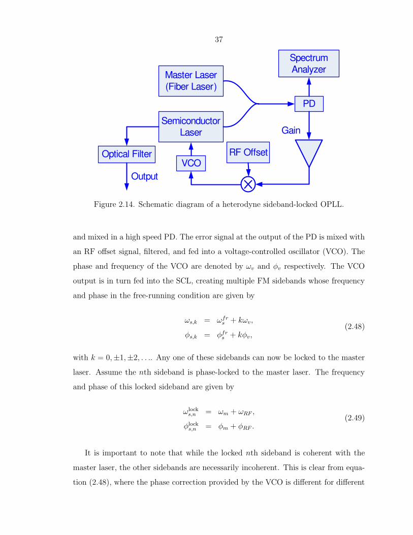
Consider the heterodyne sideband-locked OPLL system shown in figure 2.14. A
part of the SCL output is combined with the master laser using a 2 × 1 fiber coupler,
37
Semiconductor
Laser
PD
Gain
VCORF Offset
Master Laser
(Fiber Laser)
Spectrum
Analyzer
Optical Filter
Output
Figure 2.14. Schematic diagram of a heterodyne sideband-locked OPLL.
and mixed in a high speed PD. The error signal at the output of the PD is mixed with
an RF offset signal, filtered, and fed into a voltage-controlled oscillator (VCO). The
phase and frequency of the VCO are denoted by ωv and φv respectively. The VCO
output is in turn fed into the SCL, creating multiple FM sidebands whose frequency
and phase in the free-running condition are given by
ωs,k = ωfrs + kωv,
φs,k = φfrs + kφv,
(2.48)
with k = 0,±1,±2, . . .. Any one of these sidebands can now be locked to the master
laser. Assume the nth sideband is phase-locked to the master laser. The frequency
and phase of this locked sideband are given by
ωlocks,n = ωm + ωRF ,
φlocks,n = φm + φRF .
(2.49)
It is important to note that while the locked nth sideband is coherent with the
master laser, the other sidebands are necessarily incoherent. This is clear from equa-
tion (2.48), where the phase correction provided by the VCO is different for different

38
sideband orders. The other sidebands therefore have to be optically filtered out, as
shown in figure 2.14. The power in the nth sideband (normalized to the total optical
power) is given by
Pn =
∣
∣
∣
∣
Jn
(
|FFM(ωv/2π)|Av
ωv
)∣
∣
∣
∣
2
, (2.50)
where Jn is the nth order Bessel function of the first kind, and Av is the amplitude of
the modulating current at the VCO output. In order to maximize the total coherent
power, the n = 1 sideband is phase-locked, and the amplitude Av is chosen so as to
maximize the power in the first sideband. From equation (2.50), at the optimal value
of Av, 33.6% of the total power is in the first sideband. This power penalty introduced
by the filtering of the incoherent sidebands is acceptable in most applications of
OPLLs owing to the high output power of the SCLs.
The open-loop transfer function of the system shown in figure 2.14, with respect
to the phase of the first optical FM sideband is given by
G1(f) =K1F
V COFM (f)Ff(f)e
−j2πfτL
j2πf, (2.51)
where K1 is the open-loop DC gain and F V COFM (f) is the normalized FM response of
the VCO. Equation (2.51) is valid whenever the nominal VCO frequency is chosen
to be in the frequency range where the FM response of the SCL is constant. The
loop bandwidth is therefore constrained by the FM bandwidth of the VCO and the
loop propagation delay, and is independent of the thermal FM response of the laser.
If a high-bandwidth VCO is used, the loop bandwidth is limited primarily by the
propagation delay in the loop, which is what we set out to achieve in this section.
2.6.2 Experimental Demonstration
The sideband locking experiment was demonstrated using a commercially available
fiber coupled DFB SCL (Archcom Tech.) with an output power of 40 mW at 1550 nm,
and a tunable master laser with a linewidth of ∼50 kHz. The loop PD had a band-
width of 12 GHz. The measured FM response of the SCL, shown in figure 2.15,

39
104
106
108
−180
−135
−90
−50
0
Frequency (Hz). RB = 300 Hz
Phas
e (d
egre
es)
104
106
1080
0.5
1
1.5
2
Am
pli
tude
(GH
z/m
A)
Figure 2.15. Measured FM response of the DFB SCL used in the sideband lockingexperiment.
exhibits a π/2 phase-crossover at a frequency of 1.6 MHz, which is lesser than its
3 dB linewidth of 5 MHz; and the SCL therefore could not be phase-locked in the
simple heterodyne OPLL of figure 2.1. However, using the sideband-locking tech-
nique presented in this section, the first FM sideband of this SCL was successfully
phase-locked to the master laser in a fiber-based OPLL using discrete RF electronic
components. The frequencies of the VCO and the RF offset signal were chosen to be
4 GHz and 1.5 GHz respectively. The locked FM sideband was optically filtered using
a Fiber Bragg Grating with a narrow 20 dB bandwidth of 10 GHz (Orbits Lightwave,
Pasadena, CA). A suppression ratio of >25 dB to the carrier and the n = 2 sideband
was achieved in the filtered output.
The bandwidth of the fiber-based OPLL without a loop filter was about 20 MHz,
corresponding to a total loop propagation delay of 12.5 ns. By varying the fiber delay
in the loop, it was verified that the bandwidth was limited by the loop delay. A

40
1400 1450 1500 1550 1600−80
−70
−60
−50
−40
−30
−20
−10
Frequency (MHz). RB = 100 kHz VB = 3 kHz
Inte
nsi
ty (
dB
)
Figure 2.16. Beat spectrum between the locked sideband of the slave SCL and themaster laser.
passive R-C filter with the transfer function
Ff (f) =(1 + j2πfτz1)(1 + j2πfτz2)
(1 + j2πfτp1)(1 + j2πfτp2)(2.52)
was used in the loop to improve the bandwidth, with τz1 = 53.6 ns, τz2 = 1.41 µs,τp1 = 4.34 ns and τp2 = 8.71 µs. The resultant loop bandwidth was measured to
be 35 MHz and the hold-in range was ±90 MHz. The measured spectrum of the
beat signal between the phase-locked FM sideband and the master laser is shown
in figure 2.16. The locking efficiency η is calculated from the spectrum to be 80%.
This corresponds to a residual phase error variance of σ2φ = 0.25 rad2. The loop
bandwidth and the residual phase error can be further improved by reducing the loop
propagation delay.
The lineshape of the master laser and that of the filtered n = 1 sideband of the
slave SCL, measured using the delayed self-heterodyne interferometer technique, are
shown in figure 2.17. The lineshape of the locked SCL sideband follows that of the
master laser for frequencies within the loop bandwidth, and reverts to the unlocked

41
260 280 300 320−80
−70
−60
−50
−40
−30
Frequency (MHz). RB = 300 kHz VB = 100 Hz
Inte
nsi
ty (
dB
)
Unlocked
Locked
Master
Figure 2.17. Lineshape measurements of the master laser, free-running and phase-locked optical sideband of the slave SCL, using a delayed self-heterodyne interferom-eter with a frequency shift of 290 MHz.
lineshape outside the loop bandwidth.
In summary, the limitation imposed on the loop bandwidth of an OPLL using
a single section DFB SCL by the phase reversal of the laser FM response can be
overcome by locking an FM sideband of the SCL to the master laser. Using this
technique, the sideband locking of a DFB laser, which could not be locked in a simple
heterodyne OPLL, was demonstrated. A delay-limited bandwidth of 35 MHz was
achieved, which can be increased to a few hundreds of megahertz using miniature or
integrated optics and integrated RF electronic circuits. The phase-locked sideband
was optically filtered, and it was shown that the phase noise of the filtered locked
sideband was determined by that of the master laser for frequencies within the loop
bandwidth. The demonstrated approach to phase-locking SCLs facilitates the phase-
locking of standard single section DFB SCLs with moderately large linewidths, with
very little increase in system complexity.

42
2.7 Novel Phase-Lock Architectures II: Composite
OPLLs
The sideband locking approach developed in section 2.6 can be used to phase-lock
SCLs with large linewidths, but it comes with two drawbacks: (i) only a third of
the SCL output power is useful coherent power, and (ii) a narrow-band optical filter
is necessary to filter out the coherent optical sideband. While these restrictions are
acceptable in most applications, there are some others, such as OPLLs where the
frequency of the slave SCL needs to be tuned, where the use of the optical filter is
undesirable. In this section, we demonstrate an alternative solution that involves the
use of an optical phase modulator to extend the bandwidth of the loop and reduce the
residual phase error. The basic idea behind the approach is to use the phase modulator
to provide correction at higher frequencies where the thermal response of the SCL
is negligible. We demonstrate theoretically and experimentally the improvement of
loop bandwidth using two different loop configurations. The use of discrete optical
and electronic components in our proof-of-principle experiment results in a reduction
of the residual phase noise by about a factor of two; however, the use of integrated
optical phase modulators in photonic integrated circuits [22, 77] can lead to very
efficient OPLL systems.
2.7.1 System Description
2.7.1.1 Double-Loop Configuration
Consider the schematic diagram of the control system shown in figure 2.18(a). The
SCL is first phase-locked to the master laser in a heterodyne OPLL; this loop is
shown with the photodetector PD1 in the figure. The output of the phase-locked
SCL is phase modulated and mixed with the master laser in a second photodetector
PD2. The resultant error signal is down-converted, filtered, and input to the phase
modulator. The output of the phase modulator serves as the useful optical output.
The linearized small-signal model for the propagation of the optical phase in the

43
Master Laser
Slave Laser
Filter 1
PD1
Phase
Modulator
Filter 2
Gain
PD2
RF Offset
Gain
MixerMixer
PD1
Filter 1
Filter 2
Delay �S
Delay �P
Gain KP
Gain KS
( )fr
s fφ
( )fsφ
( ) ( )m RFf fφ φ+
( )
2
FMF f
j fπ ( )fFS
( )fFP
Σ
SCLΣ
Σ
Σ
( )fsφ
( )foutφ
+-
-+
PD2
++
(a)
(b)
Optical
Output
Phase Modulator
( ) ( )m RFf fφ φ+
Figure 2.18. (a) Schematic diagram of the double-loop configuration. (b) Linearizedsmall-signal model for phase propagation. PD1 and PD2 are photodetectors.

44
frequency domain is shown in figure 2.18(b). The DC gain KP is the product of the
gains of the photodetector, mixer, loop amplifier, filter, and the phase modulator. The
filter transfer function FP (f) is assumed to be normalized to unity. For notational
simplicity, in this section, we will denote the open-loop transfer function of the simple
OPLL (equation (2.10))as G(f) and drop the subscript op, and refer to the summed
laser linewidth as ∆ν.= ∆νm +∆νs.
This system can simply be analyzed as two separate feedback loops in series. The
phase φs(f) of the output of the slave laser locked to the master laser is given by
equation(2.12). The open-loop transfer function of the second loop is given by
GP (f) = KPFP (f) exp(−j2πfτP ). (2.53)
The output phase φout(f) is related to φs(f) by
φout(f) =GP (f)
1 +GP (f)(φm(f) + φRF (f)) +
1
1 +GP (f)φs(f), (2.54)
which, using equation (2.12), reduces to
φout(f) =
[
GP
1 +GP
+G
(1 +G)(1 +GP )
]
(φm + φRF ) +1
(1 +G)(1 +GP )φfrs , (2.55)
where we have omitted the argument f . The spectral density of the residual phase
error φe = φs − φm − φRF is therefore given by
Seφ(f) =
∆ν
2πf 2
∣
∣
∣
∣
1
(1 +G(f))(1 +GP (f))
∣
∣
∣
∣
2
, (2.56)
and the variance of the phase error is
σ2φ =
∫
∞
−∞
∆ν
2πf 2
∣
∣
∣
∣
1
(1 +G(f))(1 +GP (f))
∣
∣
∣
∣
2
df. (2.57)
Comparing equations (2.18) and (2.57), we see that the addition of the second feed-
back loop causes a reduction in the phase error at frequency f by a factor |1/(1 +

45
GP (f))|, and the bandwidth over which the phase noise is reduced can be extended
to beyond that of the conventional OPLL, up to the propagation delay limit.
In the preceding analysis, we have made the assumption that the optical path
lengths from the master laser and the phase-locked slave laser to the photodetector
PD2 are equal, so that the detector is biased at quadrature. (Note that the OPLL
forces the two optical fields at PD1 to be in quadrature.) In practice, path length
matching may be difficult to achieve without the use of photonic integrated circuits,
and this represents a potential drawback of this approach. Further, variations in the
relative optical path lengths result in changes in the gain seen by the second feedback
loop, resulting in larger residual phase errors. This issue is addressed in the composite
OPLL configuration discussed in the next section.
2.7.1.2 Composite PLL
The need for precise optical path length matching is eliminated in the composite PLL
architecture shown in figure 2.19(a), where the phase error measurement is performed
at a single photodetector PD. This phase error is split into two paths, one of which
drives the SCL as in a conventional OPLL, whereas the second path is connected to
the input of the optical phase modulator. The output of the phase modulator serves
as the useful optical output. The linearized small-signal model for this composite PLL
is shown in figure 2.19(b). The gain KP is again defined here as the product of the
DC gains of the photodetector, amplifier, mixer, and Filter 2. This feedback system
can be regarded as comprising an integrating path (SCL) and a proportional path
(phase modulator). The integral path has large gain only over a limited frequency
range, but this is sufficient to track typical frequency drifts of the lasers.
Defining the open-loop transfer functions of the two feedback paths as
G(f) =KSFFM(f)FS(f) exp[−j2πf(τ1 + τ2)]
j2πf,
GP (f) = KPFP (f) exp(−j2πfτ2),
(2.58)

46
Σ
PD
Filter 2
SCL
Delay τ2
Delay τ1
Gain KP+
+
+
_+
( )ffr
sφ
( )out fφ
( ) ( )m RFf fφ φ+
( )
2
FMF f
j fπ
( )PF f
( )SF f
Filter 1 Gain KS
Σ
Master Laser
Slave Laser
Filter 1
RF Offset
PDPhase
Modulator
Filter 2
Gain
Gain
(a)
(b)
Output
Figure 2.19. (a) Schematic diagram of the composite heterodyne OPLL. (b) Lin-earized small-signal model for phase propagation. PD: Photodetector.

47
the output phase is given by
φout(f) =G(f)
1 +G(f) +GP (f)(φm(f) + φRF (f)) +
1
1 +G(f)φfrs (f), (2.59)
and the variance of the residual phase error φe = φout − φm − φRF is
σ2φ =
∫
∞
−∞
∆ν
2πf 2
∣
∣
∣
∣
1
1 +G(f) +GP (f)
∣
∣
∣
∣
2
df. (2.60)
The function GP (f) is chosen so that, at frequencies larger than the FM crossover
frequency of the SCL, where the function G(f) exhibits a phase reversal, the gain in
the phase modulator arm GP (f) dominates over the gain in the SCL arm G(f). This
ensures phase correction over a larger frequency range, thereby leading to a reduced
phase error between the output optical wave and the master laser.
2.7.2 Results
2.7.2.1 Laser Frequency Modulation Response
Two commercial single-mode distributed feedback lasers operating at a wavelength of
1539 nm (JDS-Uniphase) were used in the experimental demonstration. The lasers
had a 3 dB linewidth of∼0.5 MHz, and their frequency modulation response exhibited
the characteristic phase crossover at a frequency of ∼5 MHz as shown in figure 2.20.
The FM responses of the two lasers were very similar, and only one curve is shown
for clarity. The theoretical fit to the FM response using equation (2.40) is also shown,
with fitting parameters b = 2.7 and fc = 0.76 MHz.
2.7.2.2 Numerical Calculations
The spectral density of the residual phase error in the loop, and its variance, were
numerically calculated for each of the three system configurations shown in figures
2.1, 2.18 and 2.19, using equations (2.18), (2.56) and (2.60) respectively. For the sake
of simplicity, the SCL was assumed to have a Lorenzian lineshape (white frequency
noise spectrum) with a 3 dB linewidth of 200 kHz, and an FM response as modeled

48
104
106
108
0
0.1
0.2
0.3
Mag
nit
ud
e (G
Hz/
mA
) →
104
106
108
−135
−90
−45
0
Frequency (Hz) →
Ph
ase
(deg
rees
) →
Figure 2.20. Experimentally measured frequency modulation of a single-section dis-tributed feedback semiconductor laser (solid line) and theoretical fit using equation(2.40) (circles).

49
in the preceding section. The experimentally measured linewidth of the laser is larger
than this value, owing to the deviation of the frequency noise spectrum from the ideal
white noise assumption (chapter 3, [63]). The propagation delay in each path was
assumed to be 8 ns, i.e., τS = τP = τ1 = τ2 = 8 ns. This value was chosen to be a
representative value for OPLLs constructed using fiber-optics and discrete electronic
components. The parameters of the loop filters were chosen to match the values of
the lag filters used in the experiment. The filter transfer functions were given by
FS(f) =1 + j2πfτSz1 + j2πfτSp
, (2.61)
with τSz = 24 µs and τSp = 124 µs; andFP (f) =
1 + j2πfτPz
(1 + j2πfτPp1)(1 + j2πfτPp2)2, (2.62)
with τPz = 15 ns, τPp1 = 1.3 µs, and τPp2 = 0.8 ns. The double-pole at 1/(2πτPp2) =
200 MHz approximates the finite bandwidth of the op-amp used to construct the filter
in the experiment.
With the above parameters, the value of KS was optimized to result in a minimum
residual phase error in the OPLL. With this optimal gain KS,opt, the phase modulator
gain KP was optimized to result in a minimum phase error in the double-loop and
composite PLL configurations. The calculated spectra of the residual phase error in
the loop for the different cases are plotted in figure 2.21. The values of the opti-
mum gain and the residual phase error calculated over an integration bandwidth of
±50 MHz are tabulated in table 2.2. It can be seen that the standard deviation of
the residual phase error is reduced by a factor of 3–4 due to the addition of phase
modulator control.
Note that the calculated loop performance is limited by the assumed values of
the propagation delay. The values used in the calculations are an order of magnitude
larger than the delays that can be achieved using integrated optoelectronic circuits,
and therefore the residual phase error achievable in integrated OPLL circuits is ex-

50
102
104
106
108
10−18
10−15
10−12
10−9
Frequency (Hz)
Se(f
) (r
ad2/H
z)
OPLL
Double PLL
Composite PLL
Figure 2.21. Calculated two-sided spectral densities of the residual phase error in theloop, according to equations (2.18), (2.56) and (2.60). The variance of the phase erroris the area under the curves. The values of the parameters used in the calculationsare listed in the text and in table 2.2.
Table 2.2. Parameters and results of the numerical calculations of the performanceof composite OPLLs
System type Optimal gainMin. phase error
(± 50 MHz BW)
Heterodyne OPLL KS,opt = 1.4× 10⁸Hz σφ = 0.43 rad
Double-loopKS,opt = 1.4× 10⁸Hz
σφ = 0.13 radKP,opt = 71.5
Composite PLLKS,opt = 1.4× 10⁸Hz
σφ = 0.12 radKP,opt = 65.8

51
pected to be much smaller. For example, in the composite PLL of figure 2.19, if
the delays τ1 and τ2 are decreased by one order of magnitude to be equal to 0.8 ns,
and if the time constants in the filter FP (f), viz. τPz and τPp2, are correspondingly
reduced by one order of magnitude, a minimum phase error of σφ = 0.039 rad over a
bandwidth of ±1 GHz is obtained.
2.7.2.3 Experimental Validation
The reduction in residual phase noise was demonstrated using commercial distributed
feedback lasers (JDS-Uniphase) in systems with fiber optical and discrete electronic
components (MiniCircuits, Brooklyn, NY). A fiber-coupled LiNbO3 optical phase
modulator (EOSpace, Redmond, WA) was used in the experiments, and a narrow-
linewidth fiber laser (NP Photonics) was used as the master laser. An RF electronic
offset frequency of 1.5 GHz was used in the experiments. The error in the loop
was calculated using the (heterodyne) beat signal between the master laser and the
phase-locked optical output, and integrating the spectrum.
Double-loop configuration. The double-loop configuration shown in figure 2.18
was constructed with optimized loop filters FS(f) and FP (f) as given in equations
(2.61) and (2.62), with τSz = 24 µs, τSp = 124 µs, τPz = 7.5 ns and τPp1 = 0.66 µs. Themeasured beat signals for (a) the OPLL and (b) the combined double-loop system are
shown in figure 2.22. A reduction in the residual phase error (±50 MHz bandwidth)
from 0.31 to 0.16 rad was measured.
Composite PLL. A second, similar SCL was used in the construction of the com-
posite PLL shown in figure 2.19. The loop filter parameters of equations (2.61) and
(2.62) were chosen to be τSz = 24 µs, τSp = 124 µs, τPz = 15 ns and τPp1 = 1.3 µs.The measured spectra of the beat signals corresponding to (a) a conventional hetero-
dyne OPLL using this SCL and (b) the composite PLL are shown in figure 2.23. The
residual phase error (±50 MHz bandwidth) is reduced from 0.28 to 0.13 rad.
The experimentally measured reductions in the phase noise for both the above

52
−50 −25 0 25 50
−60
−40
−20
0In
ten
sity
(d
B)
−50 −25 0 25 50
−60
−40
−20
Inte
nsi
ty (
dB
)
Frequency offset (MHz)
(a)
(b)
Figure 2.22. Measured spectrum of the beat signal between the optical output and themaster laser for an SCL in (a) a heterodyne OPLL, and (b) a double-loop feedbacksystem shown in figure 2.18. Resolution bandwidth = 30 kHz, video bandwidth =300 Hz.

53
−50 −25 0 25 50−80
−60
−40
−20
0
Inte
nsi
ty (
dB
)
−50 −25 0 25 50−80
−60
−40
−20
0
Inte
nsi
ty (
dB
)
Frequency offset (MHz)
(a)
(b)
Figure 2.23. Measured spectrum of the beat signal between the optical output andthe master laser for an SCL in (a) a heterodyne OPLL, and (b) a composite PLLshown in figure 2.19. Resolution bandwidth = 30 kHz, video bandwidth = 300 Hz.

54
systems are in fair agreement with the theoretical calculations in table 2.2. The
numerical calculations are not exact and are only representative of the expected im-
provements, since nominal values for the propagation delay and the lineshape of the
free-running SCL were assumed. We note that recent independent experiments [38,39]
have demonstrated results consistent with figure 2.21 using a feedback system similar
to the one developed and analyzed in this work.
2.7.3 Summary
We have proposed and demonstrated experimentally that the residual phase error
between the phase-locked optical output of an SCL and the master laser in an OPLL
can be further reduced by additional phase correction using an optical phase mod-
ulator. Feedback into the SCL is essential to compensate for frequency drifts of the
SCL due to environmental fluctuations. The use of the additional phase modulator
allows large loop bandwidths to be achieved, limited only by propagation delay in the
system, as opposed to nonuniformities in the response of the laser. We have demon-
strated the phase modulator can be used in two different configurations, both of which
yield a considerable reduction in the residual phase error. The experimental demon-
strations used fiber optical components and discrete electronic amplifiers and mixers,
which caused a large propagation delay and limited the loop bandwidths. The use
of integrated photonic circuits in hybrid integrated OPLL systems using these tech-
niques can enable bandwidths of up to a few gigahertz using standard single-section
semiconductor lasers and relatively little increase in system complexity.