Embed Size (px)
Citation preview
1
Chapter 2 Basic Physics of Semiconductors
2.1 Semiconductor materials and their properties
2.2 PN-junction diodes
2.3 Reverse Breakdown
CH2 Basic Physics of Semiconductors 2
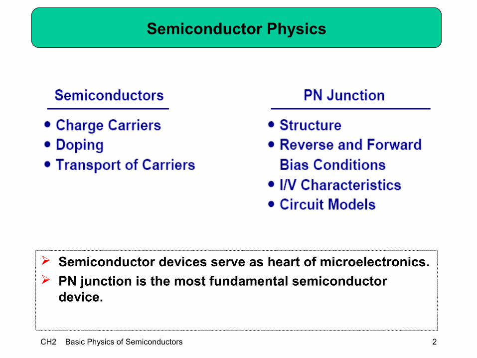
Semiconductor Physics
Semiconductor devices serve as heart of microelectronics. PN junction is the most fundamental semiconductor
device.
CH2 Basic Physics of Semiconductors 3
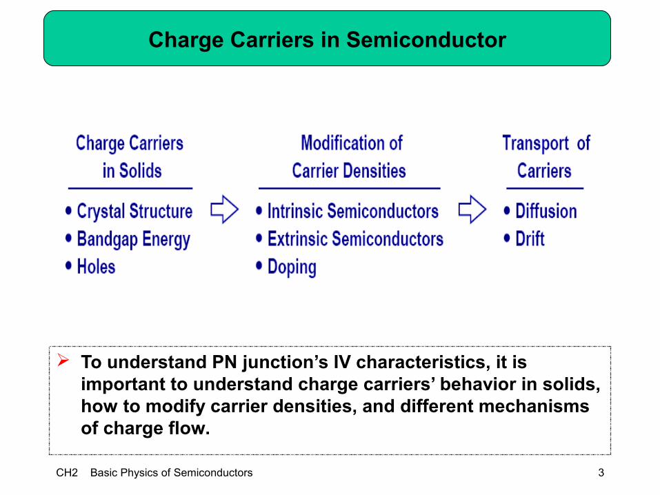
Charge Carriers in Semiconductor
To understand PN junction’s IV characteristics, it is important to understand charge carriers’ behavior in solids, how to modify carrier densities, and different mechanisms of charge flow.
CH2 Basic Physics of Semiconductors 4
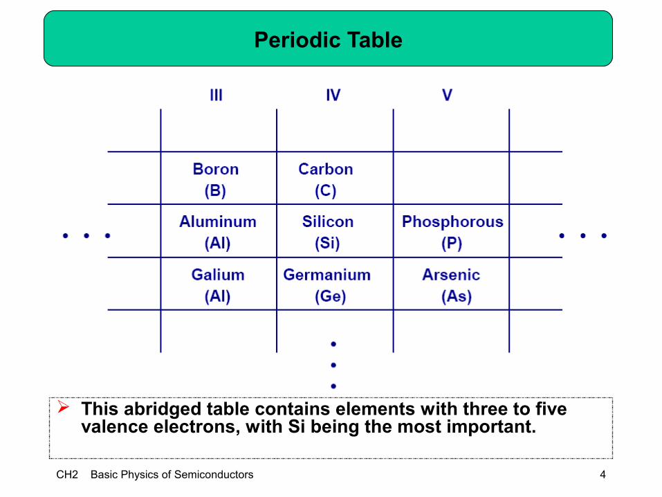
Periodic Table
This abridged table contains elements with three to five valence electrons, with Si being the most important.
CH2 Basic Physics of Semiconductors 5
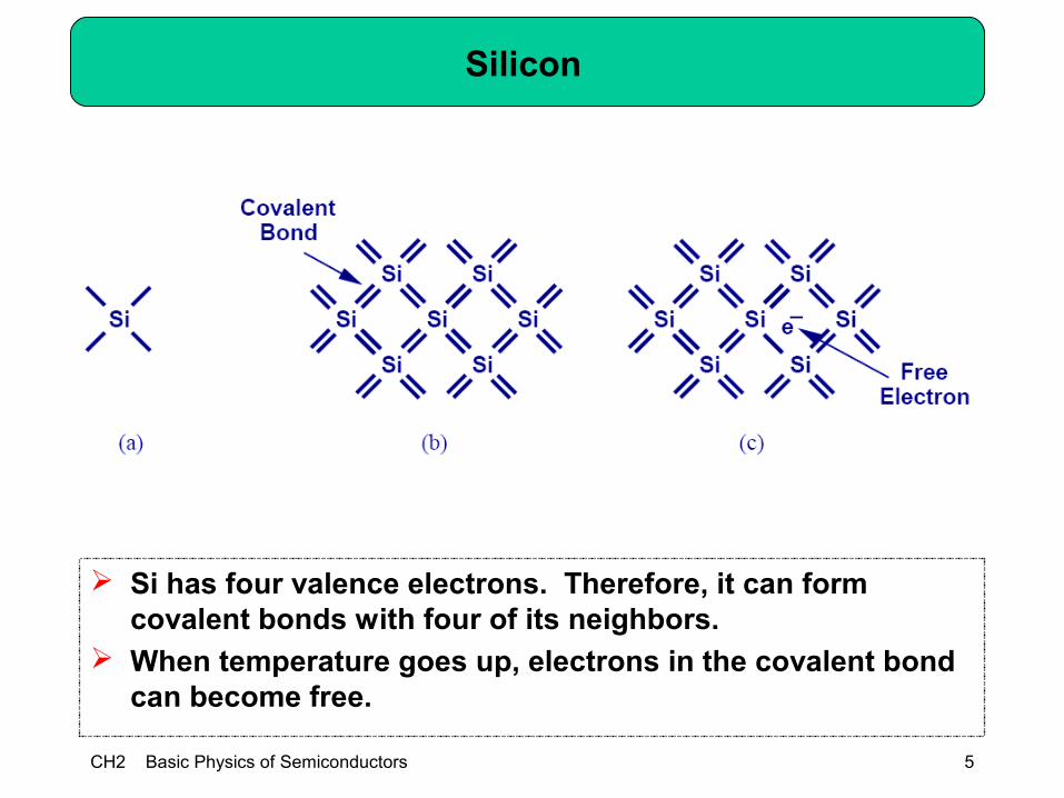
Silicon
Si has four valence electrons. Therefore, it can form covalent bonds with four of its neighbors.
When temperature goes up, electrons in the covalent bond can become free.
CH2 Basic Physics of Semiconductors 6
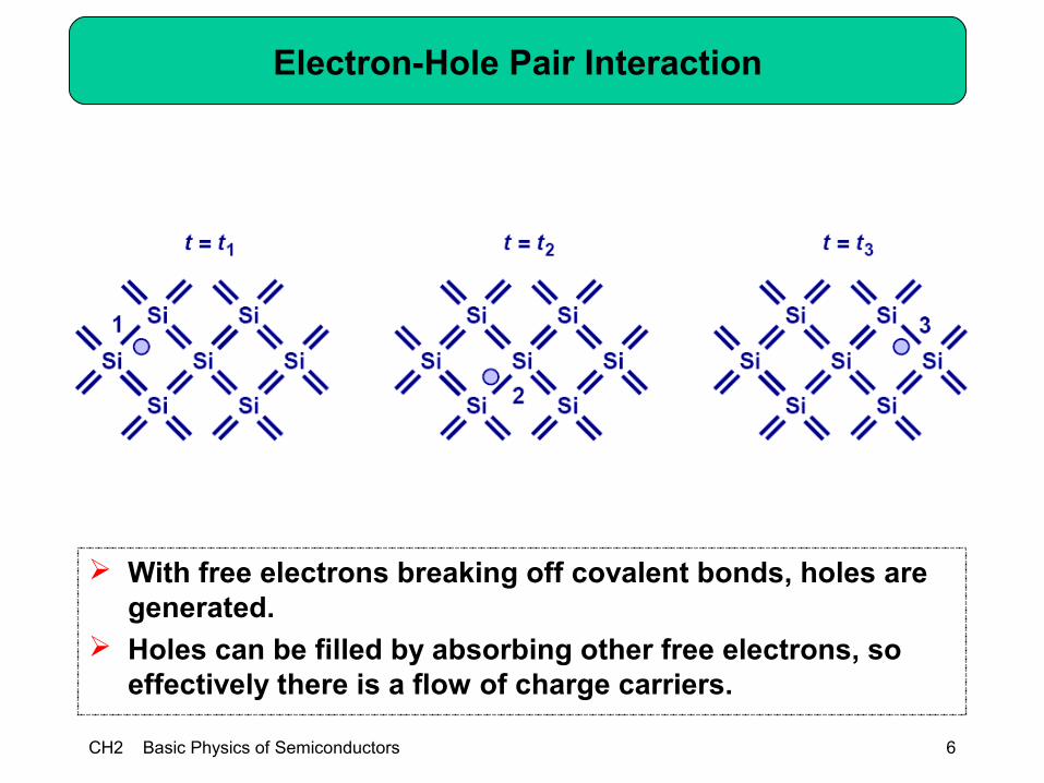
Electron-Hole Pair Interaction
With free electrons breaking off covalent bonds, holes are generated.
Holes can be filled by absorbing other free electrons, so effectively there is a flow of charge carriers.
CH2 Basic Physics of Semiconductors 7
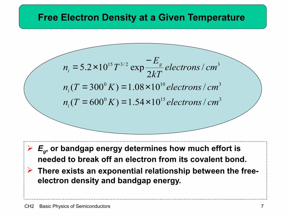
Free Electron Density at a Given Temperature
Eg, or bandgap energy determines how much effort is needed to break off an electron from its covalent bond.
There exists an exponential relationship between the free-electron density and bandgap energy.
3150
3100
32/315
/1054.1)600(
/1008.1)300(
/2
exp102.5
cmelectronsKTn
cmelectronsKTn
cmelectronskT
ETn
i
i
gi
×==×==
−×=
CH2 Basic Physics of Semiconductors 8
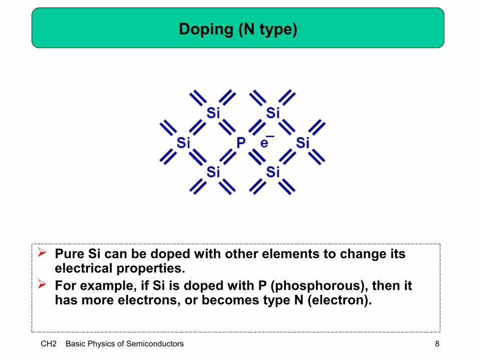
Doping (N type)
Pure Si can be doped with other elements to change its electrical properties.
For example, if Si is doped with P (phosphorous), then it has more electrons, or becomes type N (electron).
CH2 Basic Physics of Semiconductors 9
Doping (P type)
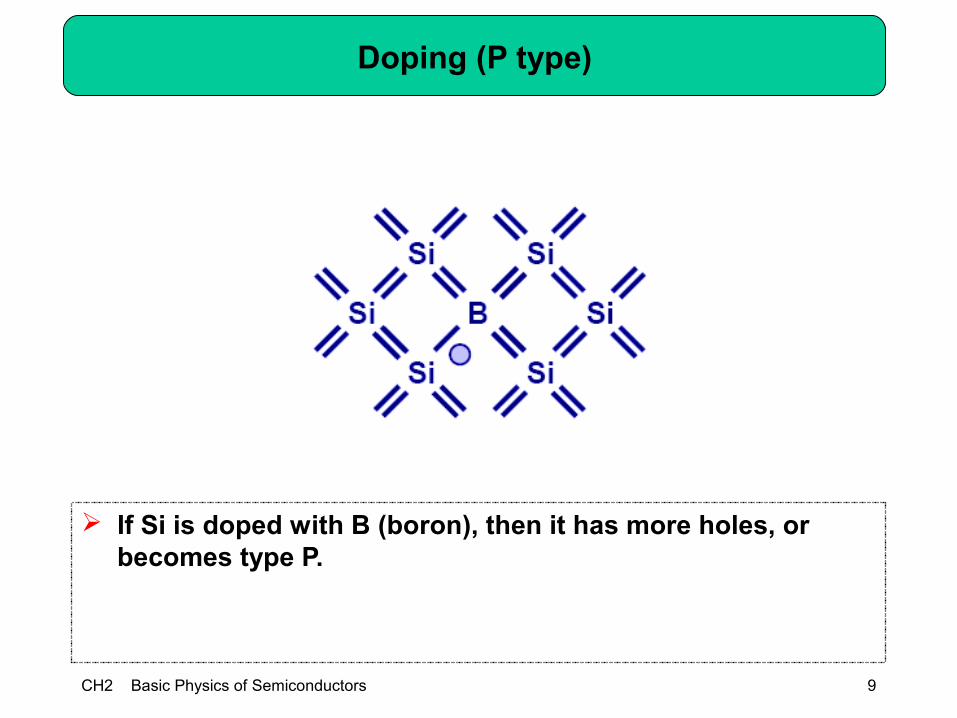
If Si is doped with B (boron), then it has more holes, or becomes type P.
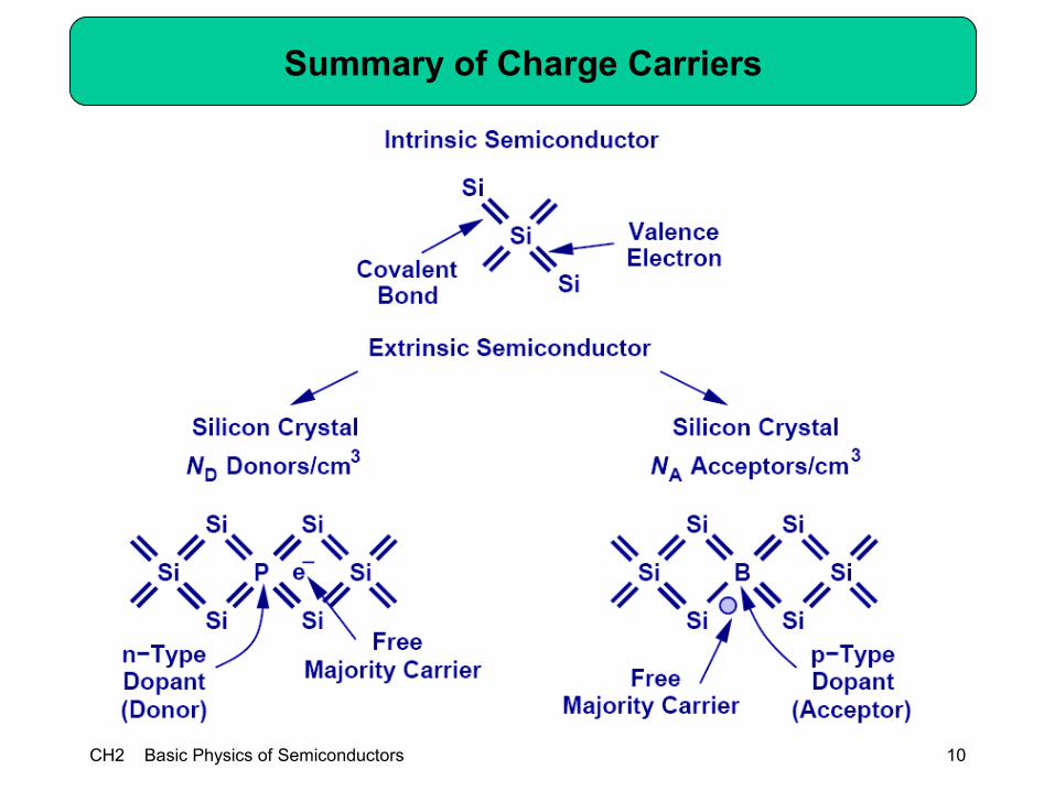
CH2 Basic Physics of Semiconductors 10
Summary of Charge Carriers
CH2 Basic Physics of Semiconductors 11
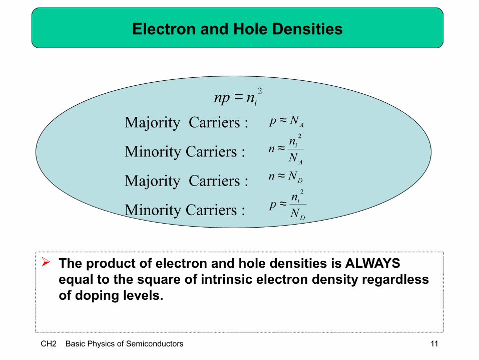
Electron and Hole Densities
The product of electron and hole densities is ALWAYS equal to the square of intrinsic electron density regardless of doping levels.
2
innp =
D
i
D
A
i
A
Nn
p
Nn
Nn
n
Np
2
2
≈
≈
≈
≈Majority Carriers :
Minority Carriers :
Majority Carriers :
Minority Carriers :
CH2 Basic Physics of Semiconductors
12
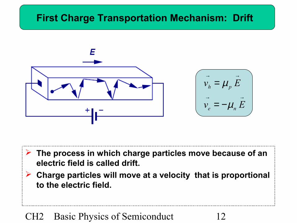
First Charge Transportation Mechanism: Drift
The process in which charge particles move because of an electric field is called drift.
Charge particles will move at a velocity that is proportional to the electric field.
→→
→→
−=
=
Ev
Ev
ne
ph
µ
µ
CH2 Basic Physics of Semiconductors
13
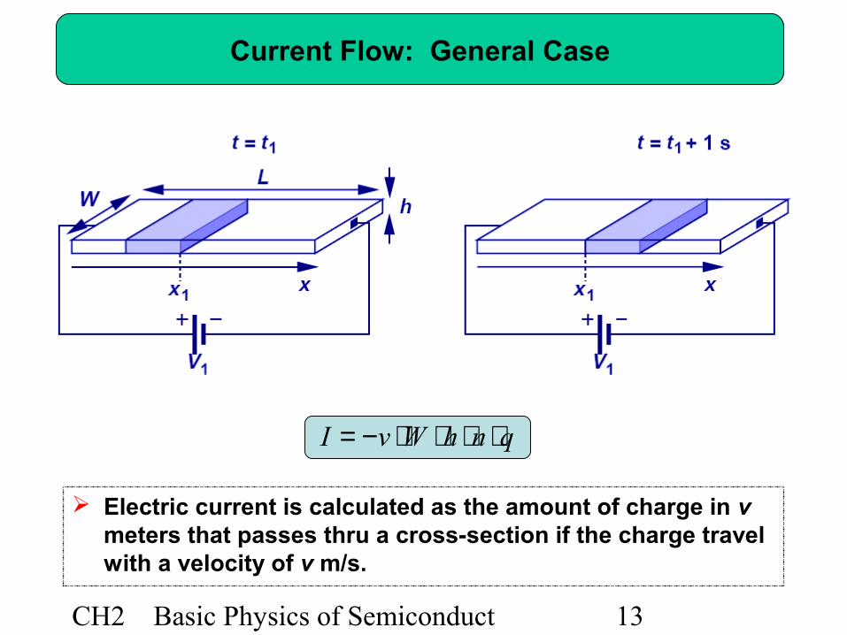
Current Flow: General Case
Electric current is calculated as the amount of charge in v meters that passes thru a cross-section if the charge travel with a velocity of v m/s.
qnhWvI ⋅⋅⋅⋅−=
CH2 Basic Physics of Semiconductors 14
Epnq
qpEqnEJ
qnEJ
pn
pntot
nn
)( µµµµ
µ
+=
⋅⋅+⋅⋅=⋅⋅=
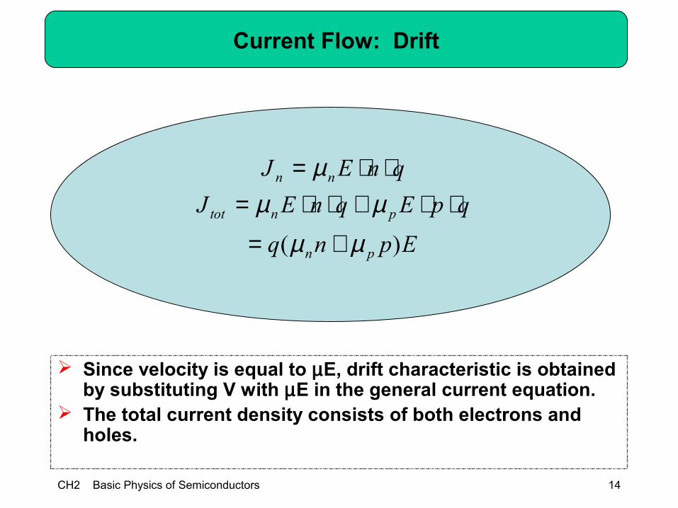
Current Flow: Drift
Since velocity is equal to µE, drift characteristic is obtained by substituting V with µE in the general current equation.
The total current density consists of both electrons and holes.
CH2 Basic Physics of Semiconductors
15
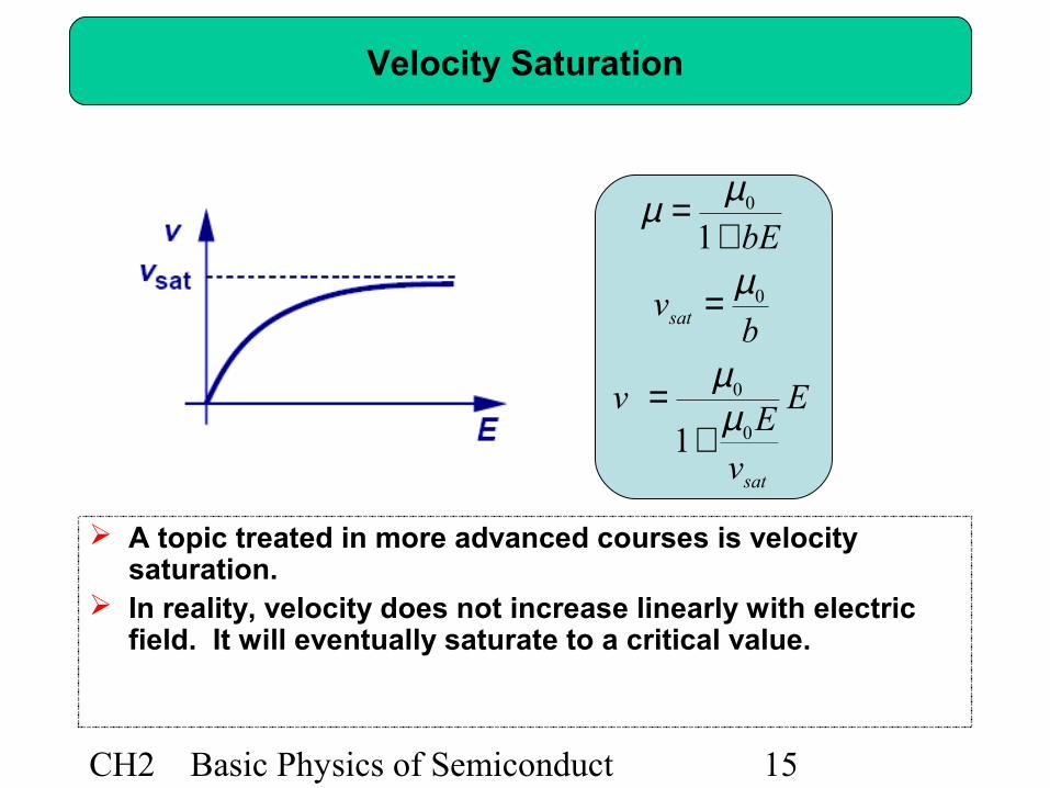
Velocity Saturation
A topic treated in more advanced courses is velocity saturation.
In reality, velocity does not increase linearly with electric field. It will eventually saturate to a critical value.
E
vE
v
bv
bE
sat
sat
0
0
0
0
1
1
µµ
µ
µµ
+=
=
+=
CH2 Basic Physics of Semiconductors 16
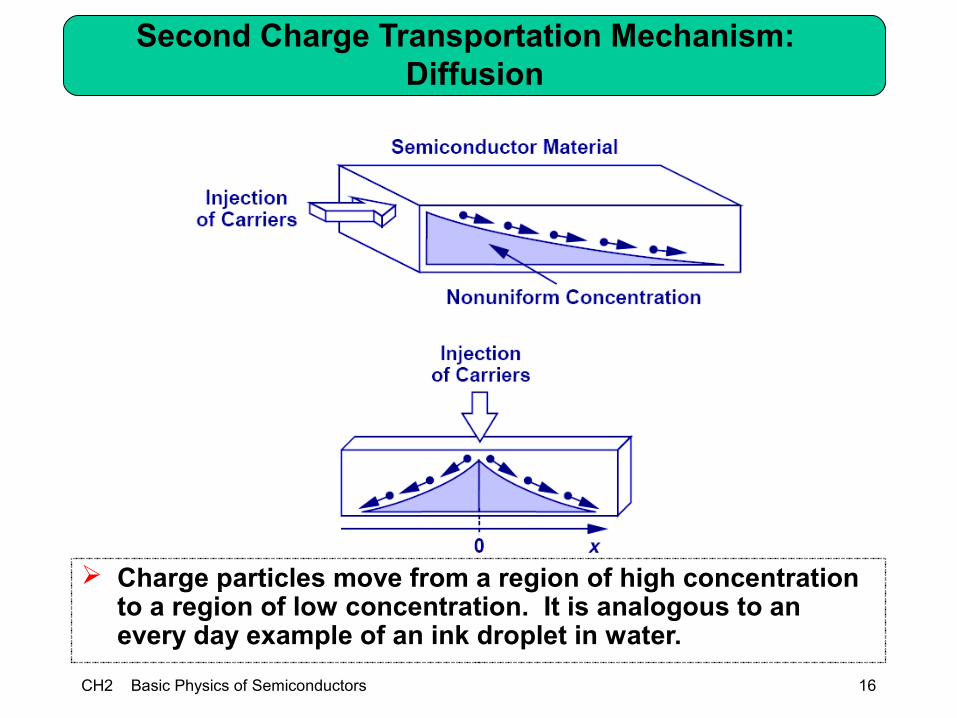
Second Charge Transportation Mechanism: Diffusion
Charge particles move from a region of high concentration to a region of low concentration. It is analogous to an every day example of an ink droplet in water.
CH2 Basic Physics of Semiconductors
17
Current Flow: Diffusion
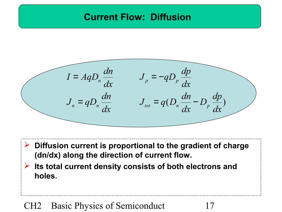
Diffusion current is proportional to the gradient of charge (dn/dx) along the direction of current flow.
Its total current density consists of both electrons and holes.
dxdn
qDJ
dxdn
AqDI
nn
n
=
=
)(dxdp
Ddxdn
DqJ
dxdp
qDJ
pntot
pp
−=
−=
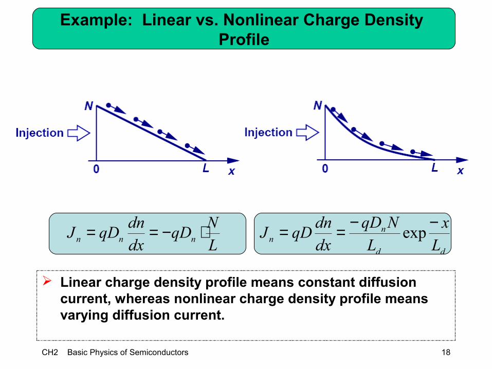
CH2 Basic Physics of Semiconductors 18
Example: Linear vs. Nonlinear Charge Density Profile
Linear charge density profile means constant diffusion current, whereas nonlinear charge density profile means varying diffusion current.
LN
qDdxdn
qDJ nnn ⋅−==dd
nn L
xL
NqDdxdn
qDJ−−== exp
CH2 Basic Physics of Semiconductors
19
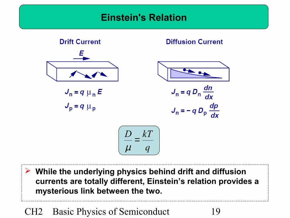
Einstein's Relation
While the underlying physics behind drift and diffusion currents are totally different, Einstein’s relation provides a mysterious link between the two.
qkTD =
µ
CH2 Basic Physics of Semiconductors 20
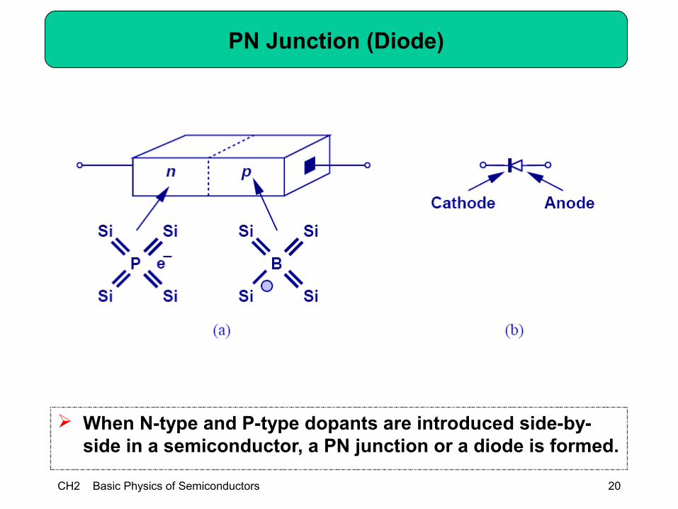
PN Junction (Diode)
When N-type and P-type dopants are introduced side-by-side in a semiconductor, a PN junction or a diode is formed.
CH2 Basic Physics of Semiconductors 21
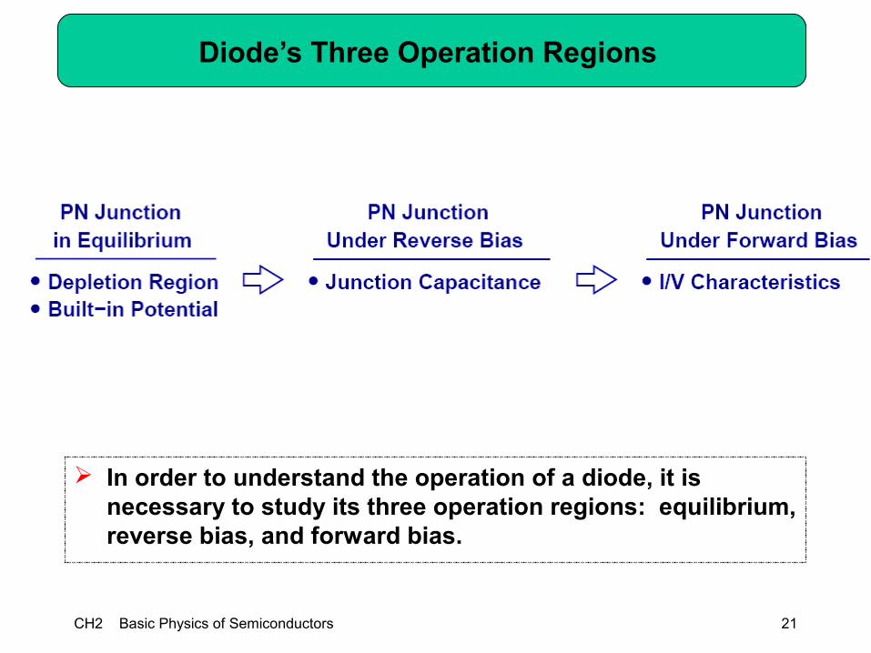
Diode’s Three Operation Regions
In order to understand the operation of a diode, it is necessary to study its three operation regions: equilibrium, reverse bias, and forward bias.
CH2 Basic Physics of Semiconductors 22
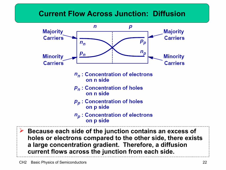
Current Flow Across Junction: Diffusion
Because each side of the junction contains an excess of holes or electrons compared to the other side, there exists a large concentration gradient. Therefore, a diffusion current flows across the junction from each side.
CH2 Basic Physics of Semiconductors
23
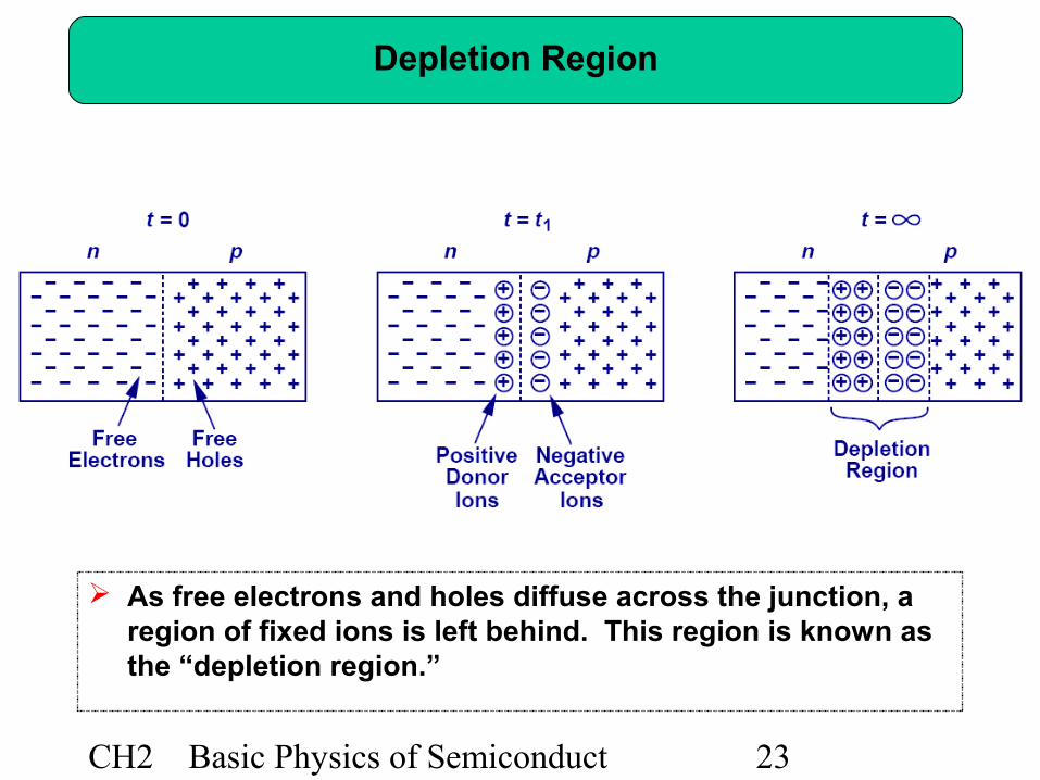
Depletion Region
As free electrons and holes diffuse across the junction, a region of fixed ions is left behind. This region is known as the “depletion region.”
CH2 Basic Physics of Semiconductors 24
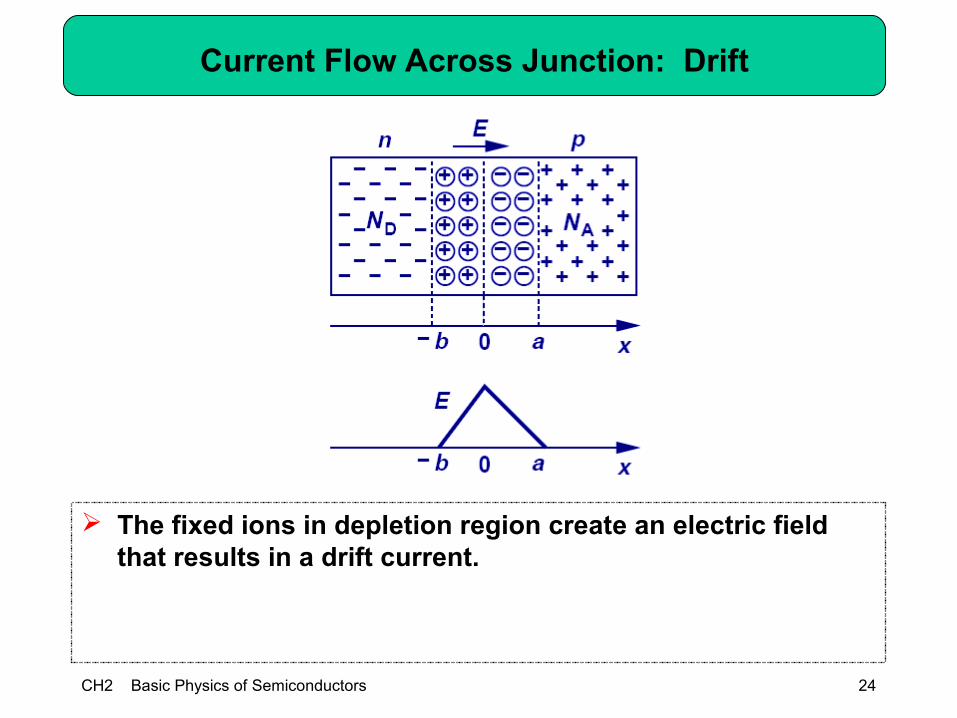
Current Flow Across Junction: Drift
The fixed ions in depletion region create an electric field that results in a drift current.
CH2 Basic Physics of Semiconductors 25
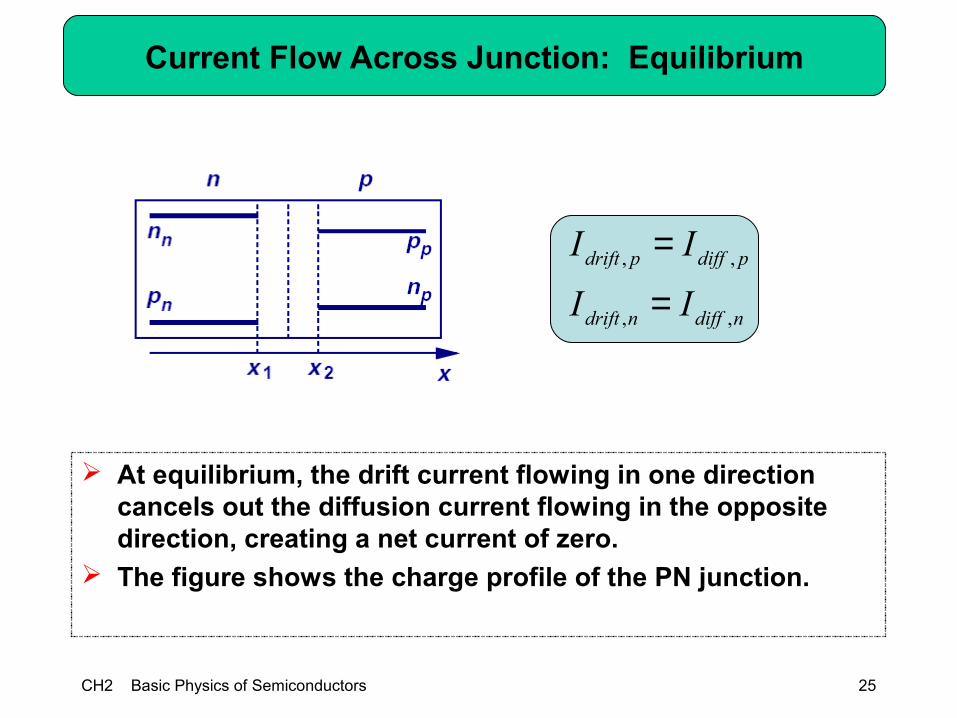
Current Flow Across Junction: Equilibrium
At equilibrium, the drift current flowing in one direction cancels out the diffusion current flowing in the opposite direction, creating a net current of zero.
The figure shows the charge profile of the PN junction.
ndiffndrift
pdiffpdrift
II
II
,,
,,
=
=
CH2 Basic Physics of Semiconductors
26
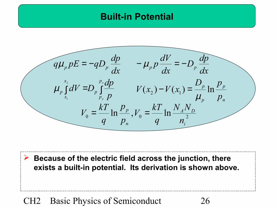
Built-in Potential
Because of the electric field across the junction, there exists a built-in potential. Its derivation is shown above.
∫∫ =
−=
n
p
p
pp
x
xp
pp
pdp
DdV
dxdp
qDpEq
2
1
µ
µ
n
p
p
p
pp
p
pDxVxV
dxdp
DdxdV
p
ln)()( 12 µ
µ
=−
−=−
200 ln,lni
DA
n
p
n
NNqkT
Vp
p
qkT
V ==
CH2 Basic Physics of Semiconductors 27
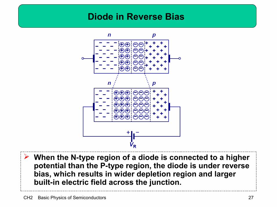
Diode in Reverse Bias
When the N-type region of a diode is connected to a higher potential than the P-type region, the diode is under reverse bias, which results in wider depletion region and larger built-in electric field across the junction.
CH2 Basic Physics of Semiconductors 28
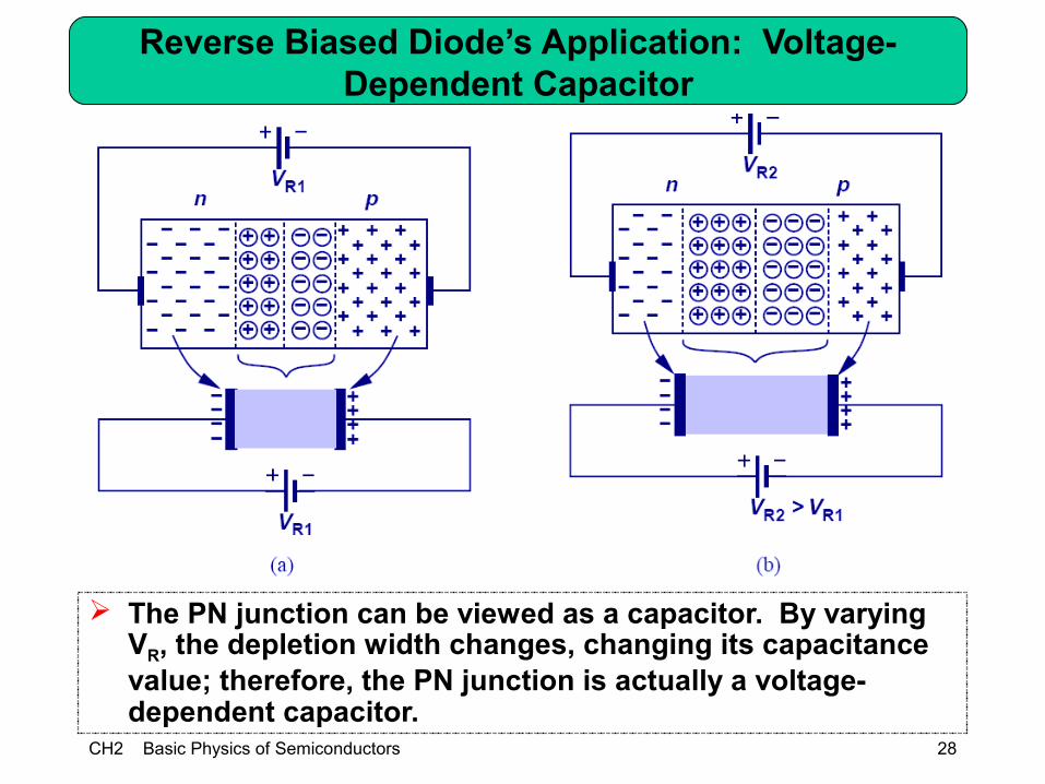
Reverse Biased Diode’s Application: Voltage-Dependent Capacitor
The PN junction can be viewed as a capacitor. By varying VR, the depletion width changes, changing its capacitance value; therefore, the PN junction is actually a voltage-dependent capacitor.
CH2 Basic Physics of Semiconductors
29
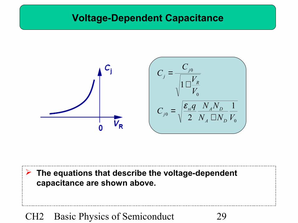
Voltage-Dependent Capacitance
The equations that describe the voltage-dependent capacitance are shown above.
0
0
0
0
1
2
1
VNN
NNqC
VV
CC
DA
DAsij
R
jj
+=
+=
ε
CH2 Basic Physics of Semiconductors
30
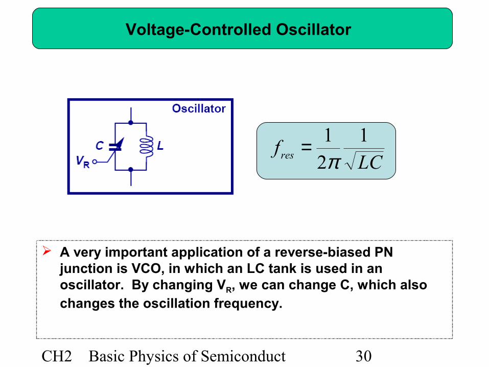
Voltage-Controlled Oscillator
A very important application of a reverse-biased PN junction is VCO, in which an LC tank is used in an oscillator. By changing VR, we can change C, which also changes the oscillation frequency.
LCf res
121π
=
CH2 Basic Physics of Semiconductors 31
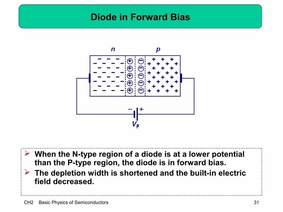
Diode in Forward Bias
When the N-type region of a diode is at a lower potential than the P-type region, the diode is in forward bias.
The depletion width is shortened and the built-in electric field decreased.
CH2 Basic Physics of Semiconductors
32
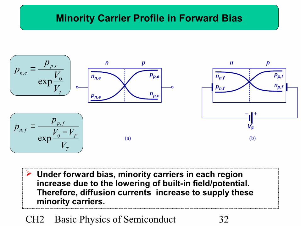
Minority Carrier Profile in Forward Bias
Under forward bias, minority carriers in each region increase due to the lowering of built-in field/potential. Therefore, diffusion currents increase to supply these minority carriers.
T
F
fpfn
VVV
pp −=
0
,,
exp
T
epen
VV
pp
0
,,
exp=
CH2 Basic Physics of Semiconductors
33
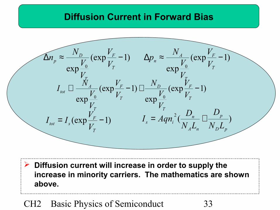
Diffusion Current in Forward Bias
Diffusion current will increase in order to supply the increase in minority carriers. The mathematics are shown above.
)1(expexp 0
−≈∆T
F
T
Dp V
V
VV
Nn )1(exp
exp 0
−≈∆T
F
T
An V
V
VV
Np
)(2
pD
p
nA
nis LN
D
LND
AqnI +=)1(exp −=T
Fstot V
VII
)1(expexp
)1(expexp 00
−+−∝T
F
T
D
T
F
T
Atot V
V
VV
NVV
VV
NI
CH2 Basic Physics of Semiconductors 34
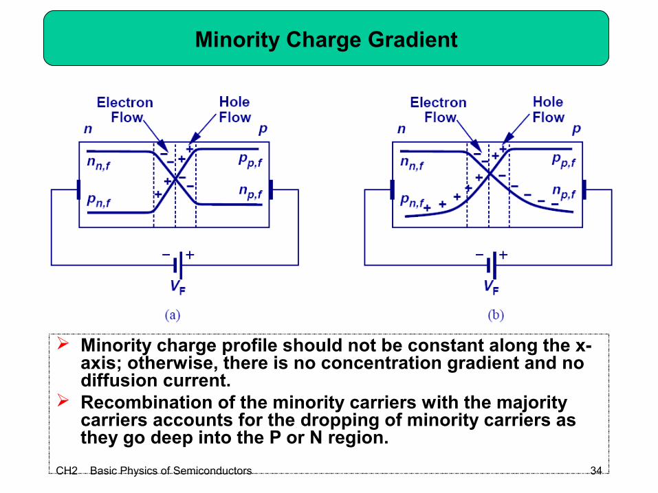
Minority Charge Gradient
Minority charge profile should not be constant along the x-axis; otherwise, there is no concentration gradient and no diffusion current.
Recombination of the minority carriers with the majority carriers accounts for the dropping of minority carriers as they go deep into the P or N region.
CH2 Basic Physics of Semiconductors 35
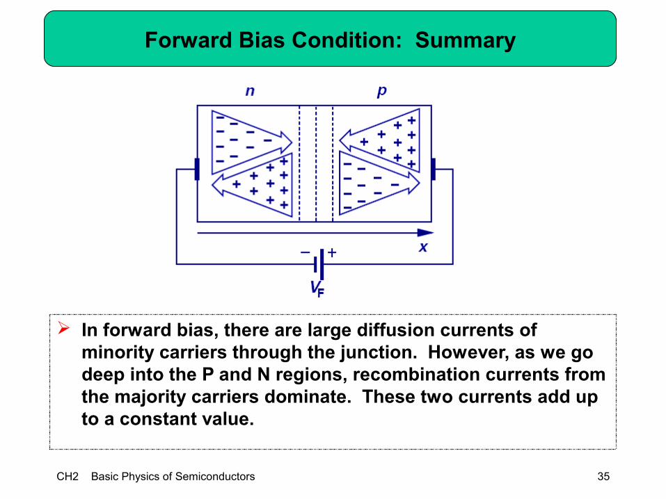
Forward Bias Condition: Summary
In forward bias, there are large diffusion currents of minority carriers through the junction. However, as we go deep into the P and N regions, recombination currents from the majority carriers dominate. These two currents add up to a constant value.
CH2 Basic Physics of Semiconductors
36
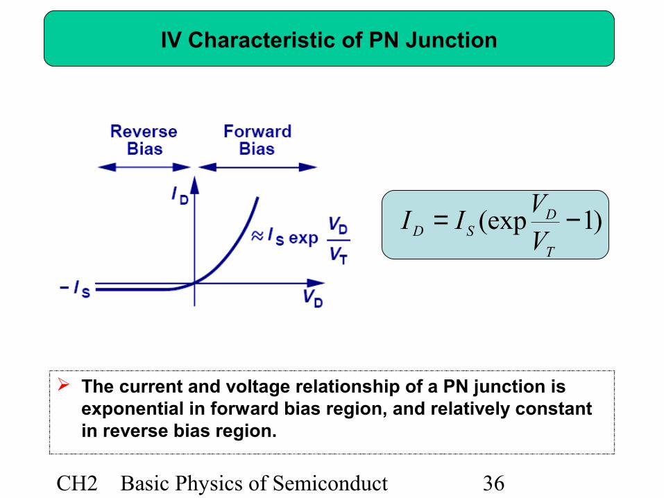
IV Characteristic of PN Junction
The current and voltage relationship of a PN junction is exponential in forward bias region, and relatively constant in reverse bias region.
)1(exp −=T
DSD V
VII
CH2 Basic Physics of Semiconductors 37
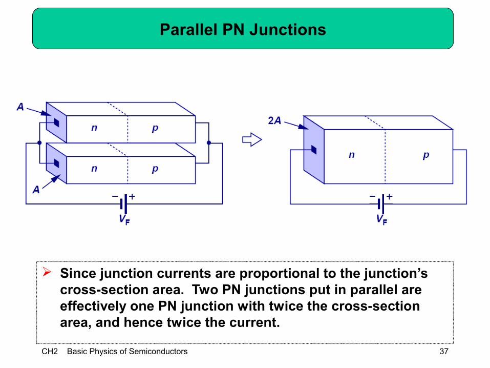
Parallel PN Junctions
Since junction currents are proportional to the junction’s cross-section area. Two PN junctions put in parallel are effectively one PN junction with twice the cross-section area, and hence twice the current.
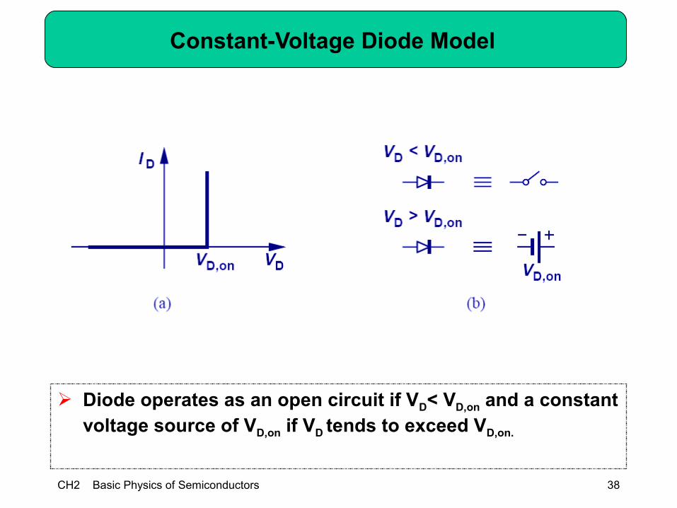
CH2 Basic Physics of Semiconductors 38
Constant-Voltage Diode Model
Diode operates as an open circuit if VD< VD,on and a constant voltage source of VD,on if VD tends to exceed VD,on.
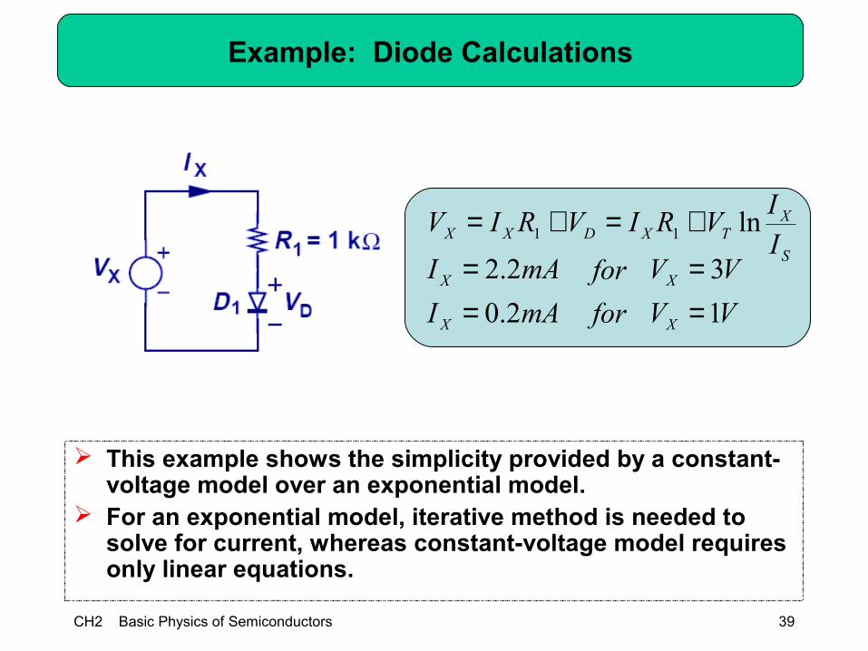
CH2 Basic Physics of Semiconductors 39
Example: Diode Calculations
This example shows the simplicity provided by a constant-voltage model over an exponential model.
For an exponential model, iterative method is needed to solve for current, whereas constant-voltage model requires only linear equations.
S
XTXDXX I
IVRIVRIV ln11 +=+=
mAI
mAI
X
X
2.0
2.2
==
VV
VV
X
X
1
3
==for
for
CH2 Basic Physics of Semiconductors 40
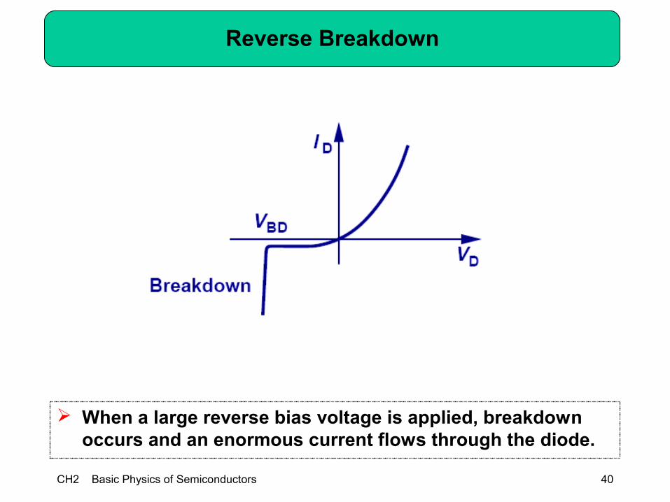
Reverse Breakdown
When a large reverse bias voltage is applied, breakdown occurs and an enormous current flows through the diode.
CH2 Basic Physics of Semiconductors 41
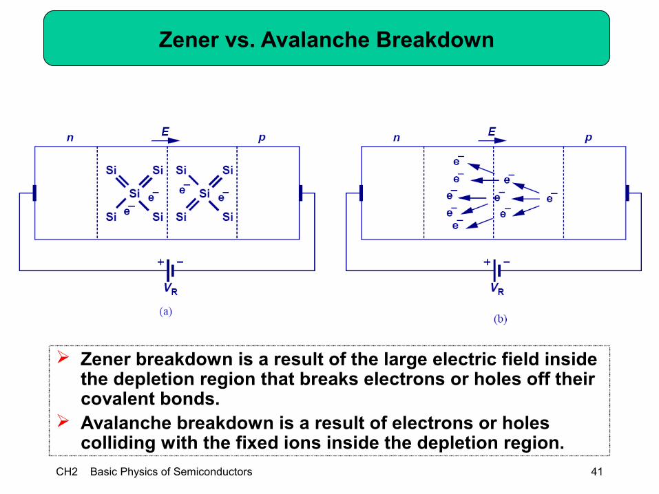
Zener vs. Avalanche Breakdown
Zener breakdown is a result of the large electric field inside the depletion region that breaks electrons or holes off their covalent bonds.
Avalanche breakdown is a result of electrons or holes colliding with the fixed ions inside the depletion region.