Embed Size (px)
Citation preview
Chapter 11: Basic I/O Interface

Copyright ©2009 by Pearson Education, Inc.
Upper Saddle River, New Jersey 07458 • All rights reserved.
The Intel Microprocessors: 8086/8088, 80186/80188, 80286, 80386, 80486 Pentium,
Pentium Pro Processor, Pentium II, Pentium, 4, and Core2 with 64-bit Extensions
Architecture, Programming, and Interfacing, Eighth Edition
Barry B. Brey
Introduction
• This chapter outlines some of the basic
methods of communications, both serial and
parallel, between humans or machines and
the microprocessor.
• We first introduce the basic I/O interface and
discuss decoding for I/O devices.
• Then, we provide detail on parallel and serial
interfacing, both of which have a variety of
applications.

Copyright ©2009 by Pearson Education, Inc.
Upper Saddle River, New Jersey 07458 • All rights reserved.
The Intel Microprocessors: 8086/8088, 80186/80188, 80286, 80386, 80486 Pentium,
Pentium Pro Processor, Pentium II, Pentium, 4, and Core2 with 64-bit Extensions
Architecture, Programming, and Interfacing, Eighth Edition
Barry B. Brey
Chapter Objectives
• Explain the operation of the basic input and
output interfaces.
• Decode an 8-, 16-, and 32-bit I/O device so
that they can be used at any I/O port address.
• Define handshaking and explain how to use it
with I/O devices.
• Interface and program the 82C55
programmable parallel interface.
Upon completion of this chapter, you will be able to:
Copyright ©2009 by Pearson Education, Inc.
Upper Saddle River, New Jersey 07458 • All rights reserved.
The Intel Microprocessors: 8086/8088, 80186/80188, 80286, 80386, 80486 Pentium,
Pentium Pro Processor, Pentium II, Pentium, 4, and Core2 with 64-bit Extensions
Architecture, Programming, and Interfacing, Eighth Edition
Barry B. Brey
Chapter Objectives
• Interface LCD displays, LED displays,
keyboards, ADC, DAC, and various other
devices to the 82C55.
• Interface and program the 16550 serial
communications interface adapter.
• Interface and program the 8254
programmable interval timer.
Upon completion of this chapter, you will be able to:
(cont.)

Copyright ©2009 by Pearson Education, Inc.
Upper Saddle River, New Jersey 07458 • All rights reserved.
The Intel Microprocessors: 8086/8088, 80186/80188, 80286, 80386, 80486 Pentium,
Pentium Pro Processor, Pentium II, Pentium, 4, and Core2 with 64-bit Extensions
Architecture, Programming, and Interfacing, Eighth Edition
Barry B. Brey
Chapter Objectives
• Interface an analog-to-digital converter and a
digital-to-analog converter to the
microprocessor.
• Interface both DC and stepper motors to the
microprocessor.
Upon completion of this chapter, you will be able to:
(cont.)

Copyright ©2009 by Pearson Education, Inc.
Upper Saddle River, New Jersey 07458 • All rights reserved.
The Intel Microprocessors: 8086/8088, 80186/80188, 80286, 80386, 80486 Pentium,
Pentium Pro Processor, Pentium II, Pentium, 4, and Core2 with 64-bit Extensions
Architecture, Programming, and Interfacing, Eighth Edition
Barry B. Brey
11–1 INTRO TO I/O INTERFACE
• I/O instructions (IN, INS, OUT, and OUTS) are
explained.
• Also isolated (direct or I/O mapped I/O) and
memory-mapped I/O, the basic input and
output interfaces, and handshaking.
• Knowledge of these topics makes it easier to
understand the connection and operation of
the programmable interface components
and I/O techniques.
Copyright ©2009 by Pearson Education, Inc.
Upper Saddle River, New Jersey 07458 • All rights reserved.
The Intel Microprocessors: 8086/8088, 80186/80188, 80286, 80386, 80486 Pentium,
Pentium Pro Processor, Pentium II, Pentium, 4, and Core2 with 64-bit Extensions
Architecture, Programming, and Interfacing, Eighth Edition
Barry B. Brey
The I/O Instructions
• One type of instruction transfers information
to an I/O device (OUT).
• Another reads from an I/O device (IN).
• Instructions are also provided to transfer
strings of data between memory and I/O.
– INS and OUTS, found except the 8086/8088

Copyright ©2009 by Pearson Education, Inc.
Upper Saddle River, New Jersey 07458 • All rights reserved.
The Intel Microprocessors: 8086/8088, 80186/80188, 80286, 80386, 80486 Pentium,
Pentium Pro Processor, Pentium II, Pentium, 4, and Core2 with 64-bit Extensions
Architecture, Programming, and Interfacing, Eighth Edition
Barry B. Brey
• Instructions that transfer data between an I/O
device and the microprocessor’s accumulator
(AL, AX, or EAX) are called IN and OUT.
• The I/O address is stored in register DX as a
16-bit address or in the byte (p8) immediately
following the opcode as an 8-bit address.
– Intel calls the 8-bit form (p8) a fixed address
because it is stored with the instruction, usually
in a ROM
• The 16-bit address is called a variable
address because it is stored in a DX, and
then used to address the I/O device.

Copyright ©2009 by Pearson Education, Inc.
Upper Saddle River, New Jersey 07458 • All rights reserved.
The Intel Microprocessors: 8086/8088, 80186/80188, 80286, 80386, 80486 Pentium,
Pentium Pro Processor, Pentium II, Pentium, 4, and Core2 with 64-bit Extensions
Architecture, Programming, and Interfacing, Eighth Edition
Barry B. Brey
• Other instructions that use DX to address
I/O are the INS and OUTS instructions.
• I/O ports are 8 bits in width.
– a 16-bit port is actually two consecutive 8-bit
ports being addressed
– a 32-bit I/O port is actually four 8-bit ports

Copyright ©2009 by Pearson Education, Inc.
Upper Saddle River, New Jersey 07458 • All rights reserved.
The Intel Microprocessors: 8086/8088, 80186/80188, 80286, 80386, 80486 Pentium,
Pentium Pro Processor, Pentium II, Pentium, 4, and Core2 with 64-bit Extensions
Architecture, Programming, and Interfacing, Eighth Edition
Barry B. Brey
• When data are transferred using IN or OUT,
the I/O address, (port number or simply
port), appears on the address bus.
• External I/O interface decodes the port
number in the same manner as a memory
address.
– the 8-bit fixed port number (p8) appears on
address bus connections A7–A0 with bits
A15–A8 equal to 000000002
– connections above A15 are undefined for
I/O instruction

Copyright ©2009 by Pearson Education, Inc.
Upper Saddle River, New Jersey 07458 • All rights reserved.
The Intel Microprocessors: 8086/8088, 80186/80188, 80286, 80386, 80486 Pentium,
Pentium Pro Processor, Pentium II, Pentium, 4, and Core2 with 64-bit Extensions
Architecture, Programming, and Interfacing, Eighth Edition
Barry B. Brey
• The 16-bit variable port number (DX)
appears on address connections A15–A0.
• The first 256 I/O port addresses (00H–FFH)
are accessed by both fixed and variable I/O
instructions.
– any I/O address from 0100H to FFFFH
is only accessed by the variable I/O address
• In a PC computer, all 16 address bus bits
are decoded with locations 0000H–03FFH.
– used for I/O inside the PC on the ISA
(industry standard architecture) bus

Copyright ©2009 by Pearson Education, Inc.
Upper Saddle River, New Jersey 07458 • All rights reserved.
The Intel Microprocessors: 8086/8088, 80186/80188, 80286, 80386, 80486 Pentium,
Pentium Pro Processor, Pentium II, Pentium, 4, and Core2 with 64-bit Extensions
Architecture, Programming, and Interfacing, Eighth Edition
Barry B. Brey
• INS and OUTS instructions address an I/O
device using the DX register.
– but do not transfer data between accumulator
and I/O device as do the IN/OUT instructions
– Instead, they transfer data between memory
and the I/O device
• Pentium 4 and Core2 operating in the 64-bit
mode have the same I/O instructions.
• There are no 64-bit I/O instructions in the 64-
bit mode.
– most I/O is still 8 bits and likely will remain so

Copyright ©2009 by Pearson Education, Inc.
Upper Saddle River, New Jersey 07458 • All rights reserved.
The Intel Microprocessors: 8086/8088, 80186/80188, 80286, 80386, 80486 Pentium,
Pentium Pro Processor, Pentium II, Pentium, 4, and Core2 with 64-bit Extensions
Architecture, Programming, and Interfacing, Eighth Edition
Barry B. Brey
Isolated and Memory-Mapped I/O
• Two different methods of interfacing I/O:
isolated I/O and memory-mapped I/O.
• In isolated I/O, the IN, INS, OUT, and OUTS
transfer data between the microprocessor’s
accumulator or memory and the I/O device.
• In memory-mapped I/O, any instruction that
references memory can accomplish the
transfer.
• The PC does not use memory-mapped I/O.

Copyright ©2009 by Pearson Education, Inc.
Upper Saddle River, New Jersey 07458 • All rights reserved.
The Intel Microprocessors: 8086/8088, 80186/80188, 80286, 80386, 80486 Pentium,
Pentium Pro Processor, Pentium II, Pentium, 4, and Core2 with 64-bit Extensions
Architecture, Programming, and Interfacing, Eighth Edition
Barry B. Brey
Isolated I/O
• The most common I/O transfer technique
used in the Intel-based system is isolated I/O.
– isolated describes how I/O locations are isolated
from memory in a separate I/O address space
• Addresses for isolated I/O devices, called
ports, are separate from memory.
• Because the ports are separate, the user can
expand the memory to its full size without
using any of memory space for I/O devices.
Copyright ©2009 by Pearson Education, Inc.
Upper Saddle River, New Jersey 07458 • All rights reserved.
The Intel Microprocessors: 8086/8088, 80186/80188, 80286, 80386, 80486 Pentium,
Pentium Pro Processor, Pentium II, Pentium, 4, and Core2 with 64-bit Extensions
Architecture, Programming, and Interfacing, Eighth Edition
Barry B. Brey
• A disadvantage of isolated I/O is that data
transferred between I/O and microprocessor
must be accessed by the IN, INS, OUT, and
OUTS instructions.
• Separate control signals for the I/O space are
developed (using M/IO and W/R ), which
indicate an I/O read (IORC) or an I/O write
(RD) operation.
• These signals indicate an I/O port address,
which appears on the address bus, is used
to select the I/O device.

Copyright ©2009 by Pearson Education, Inc.
Upper Saddle River, New Jersey 07458 • All rights reserved.
The Intel Microprocessors: 8086/8088, 80186/80188, 80286, 80386, 80486 Pentium,
Pentium Pro Processor, Pentium II, Pentium, 4, and Core2 with 64-bit Extensions
Architecture, Programming, and Interfacing, Eighth Edition
Barry B. Brey
Figure 11–1 The memory and I/O maps for the 8086/8088 microprocessors. (a)
Isolated I/O. (b) Memory-mapped I/O.
– in the PC, isolated I/O
ports are used to control
peripheral devices
– an 8-bit port address is
used to access devices
located on the system
board, such as the timer
and keyboard interface
– a 16-bit port is used to
access serial and parallel
ports, video and disk drive
systems
Copyright ©2009 by Pearson Education, Inc.
Upper Saddle River, New Jersey 07458 • All rights reserved.
The Intel Microprocessors: 8086/8088, 80186/80188, 80286, 80386, 80486 Pentium,
Pentium Pro Processor, Pentium II, Pentium, 4, and Core2 with 64-bit Extensions
Architecture, Programming, and Interfacing, Eighth Edition
Barry B. Brey
Memory-Mapped I/O
• Memory-mapped I/O does not use the IN, INS,
OUT, or OUTS instructions.
• It uses any instruction that transfers data
between the microprocessor and memory.
– treated as a memory location in memory map
• Advantage is any memory transfer instruction
can access the I/O device.
• Disadvantage is a portion of memory system
is used as the I/O map.
– reduces memory available to applications
Copyright ©2009 by Pearson Education, Inc.
Upper Saddle River, New Jersey 07458 • All rights reserved.
The Intel Microprocessors: 8086/8088, 80186/80188, 80286, 80386, 80486 Pentium,
Pentium Pro Processor, Pentium II, Pentium, 4, and Core2 with 64-bit Extensions
Architecture, Programming, and Interfacing, Eighth Edition
Barry B. Brey
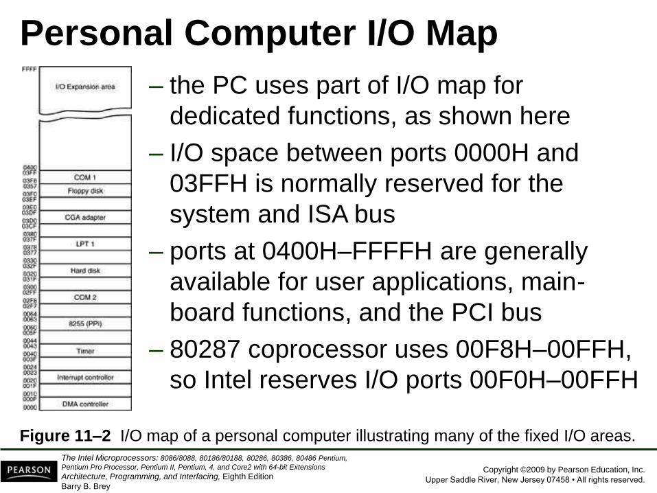
Figure 11–2 I/O map of a personal computer illustrating many of the fixed I/O areas.
Personal Computer I/O Map
– the PC uses part of I/O map for
dedicated functions, as shown here
– I/O space between ports 0000H and
03FFH is normally reserved for the
system and ISA bus
– ports at 0400H–FFFFH are generally
available for user applications, main-
board functions, and the PCI bus
– 80287 coprocessor uses 00F8H–00FFH,
so Intel reserves I/O ports 00F0H–00FFH

Copyright ©2009 by Pearson Education, Inc.
Upper Saddle River, New Jersey 07458 • All rights reserved.
The Intel Microprocessors: 8086/8088, 80186/80188, 80286, 80386, 80486 Pentium,
Pentium Pro Processor, Pentium II, Pentium, 4, and Core2 with 64-bit Extensions
Architecture, Programming, and Interfacing, Eighth Edition
Barry B. Brey
Basic Input and Output Interfaces
• The basic input device is a set of three-state
buffers.
• The basic output device is a set of data
latches.
• The term IN refers to moving data from the
I/O device into the microprocessor and
• The term OUT refers to moving data out of
the microprocessor to the I/O device.

Copyright ©2009 by Pearson Education, Inc.
Upper Saddle River, New Jersey 07458 • All rights reserved.
The Intel Microprocessors: 8086/8088, 80186/80188, 80286, 80386, 80486 Pentium,
Pentium Pro Processor, Pentium II, Pentium, 4, and Core2 with 64-bit Extensions
Architecture, Programming, and Interfacing, Eighth Edition
Barry B. Brey
The Basic Input Interface
• Three-state buffers are used to construct the
8-bit input port depicted in Figure 11–3.
• External TTL data are connected to the inputs
of the buffers.
– buffer outputs connect to the data bus
• The circuit of allows the processor to read the
contents of the eight switches that connect to
any 8-bit section of the data bus when the
select signal becomes a logic 0.

Copyright ©2009 by Pearson Education, Inc.
Upper Saddle River, New Jersey 07458 • All rights reserved.
The Intel Microprocessors: 8086/8088, 80186/80188, 80286, 80386, 80486 Pentium,
Pentium Pro Processor, Pentium II, Pentium, 4, and Core2 with 64-bit Extensions
Architecture, Programming, and Interfacing, Eighth Edition
Barry B. Brey
Figure 11–3 The basic input interface illustrating the connection of eight switches.
Note that the 74ALS244 is a three-state buffer that controls the application of the
switch data to the data bus.

Copyright ©2009 by Pearson Education, Inc.
Upper Saddle River, New Jersey 07458 • All rights reserved.
The Intel Microprocessors: 8086/8088, 80186/80188, 80286, 80386, 80486 Pentium,
Pentium Pro Processor, Pentium II, Pentium, 4, and Core2 with 64-bit Extensions
Architecture, Programming, and Interfacing, Eighth Edition
Barry B. Brey
• When the IN instruction executes, contents
of the switches copy to the AL register.
• This basic input circuit is not optional and
must appear any time input data are
interfaced to the microprocessor.
• Sometimes it appears as a discrete part of the
circuit, as shown in Figure 11–3.
– also built into a programmable I/O devices
• Sixteen- or 32-bit data can also be interfaced
but is not nearly as common as 8-bit data.

Copyright ©2009 by Pearson Education, Inc.
Upper Saddle River, New Jersey 07458 • All rights reserved.
The Intel Microprocessors: 8086/8088, 80186/80188, 80286, 80386, 80486 Pentium,
Pentium Pro Processor, Pentium II, Pentium, 4, and Core2 with 64-bit Extensions
Architecture, Programming, and Interfacing, Eighth Edition
Barry B. Brey
The Basic Output Interface
• Receives data from the processor and usually
must hold it for some external device.
– latches or flip-flops, like buffers in the input
device, are often built into the I/O device
• Fig 11–4 shows how eight light-emitting
diodes (LEDs) connect to the processor
through a set of eight data latches.
• The latch stores the number output by the
microprocessor from the data bus so that the
LEDs can be lit with any 8-bit binary number.

Copyright ©2009 by Pearson Education, Inc.
Upper Saddle River, New Jersey 07458 • All rights reserved.
The Intel Microprocessors: 8086/8088, 80186/80188, 80286, 80386, 80486 Pentium,
Pentium Pro Processor, Pentium II, Pentium, 4, and Core2 with 64-bit Extensions
Architecture, Programming, and Interfacing, Eighth Edition
Barry B. Brey
Figure 11–4 The basic output interface connected to a set of LED displays.
Copyright ©2009 by Pearson Education, Inc.
Upper Saddle River, New Jersey 07458 • All rights reserved.
The Intel Microprocessors: 8086/8088, 80186/80188, 80286, 80386, 80486 Pentium,
Pentium Pro Processor, Pentium II, Pentium, 4, and Core2 with 64-bit Extensions
Architecture, Programming, and Interfacing, Eighth Edition
Barry B. Brey
• Latches hold the data because when the
processor executes an OUT, data are only
present on the data bus for less than 1.0 µs.
– the viewer would never see the LEDs illuminate
• When the OUT executes, data from AL, AX,
or EAX transfer to the latch via the data bus.
• Each time the OUT executes, the SEL signal
activates, capturing data to the latch.
– data are held until the next OUT
• When the output instruction is executed, data
from the AL register appear on the LEDs.

Copyright ©2009 by Pearson Education, Inc.
Upper Saddle River, New Jersey 07458 • All rights reserved.
The Intel Microprocessors: 8086/8088, 80186/80188, 80286, 80386, 80486 Pentium,
Pentium Pro Processor, Pentium II, Pentium, 4, and Core2 with 64-bit Extensions
Architecture, Programming, and Interfacing, Eighth Edition
Barry B. Brey
Handshaking
• Many I/O devices accept or release
information slower than the microprocessor.
• A method of I/O control called handshaking
or polling, synchronizes the I/O device with
the microprocessor.
• An example is a parallel printer that prints a
few hundred characters per second (CPS).
• The processor can send data much faster.
– a way to slow the microprocessor down to match
speeds with the printer must be developed

Copyright ©2009 by Pearson Education, Inc.
Upper Saddle River, New Jersey 07458 • All rights reserved.
The Intel Microprocessors: 8086/8088, 80186/80188, 80286, 80386, 80486 Pentium,
Pentium Pro Processor, Pentium II, Pentium, 4, and Core2 with 64-bit Extensions
Architecture, Programming, and Interfacing, Eighth Edition
Barry B. Brey
• Fig 11–5 illustrates typical input and output
connections found on a printer.
– data transfers via data connections (D7–D0)
• ASCII data are placed on D7–D0, and a pulse
is then applied to the STB connection.
– BUSY indicates the printer is busy
– STB is a clock pulse used to send data to printer
• The strobe signal sends or clocks the data
into the printer so that they can be printed.
– as the printer receives data, it places logic 1 on
the BUSY pin, indicating it is printing data

Copyright ©2009 by Pearson Education, Inc.
Upper Saddle River, New Jersey 07458 • All rights reserved.
The Intel Microprocessors: 8086/8088, 80186/80188, 80286, 80386, 80486 Pentium,
Pentium Pro Processor, Pentium II, Pentium, 4, and Core2 with 64-bit Extensions
Architecture, Programming, and Interfacing, Eighth Edition
Barry B. Brey
Figure 11–5 The DB25 connector found on computers and the Centronics 36-pin
connector found on printers for the Centronics parallel printer interface.

Copyright ©2009 by Pearson Education, Inc.
Upper Saddle River, New Jersey 07458 • All rights reserved.
The Intel Microprocessors: 8086/8088, 80186/80188, 80286, 80386, 80486 Pentium,
Pentium Pro Processor, Pentium II, Pentium, 4, and Core2 with 64-bit Extensions
Architecture, Programming, and Interfacing, Eighth Edition
Barry B. Brey
• The software polls or tests the BUSY pin to
decide whether the printer is busy.
– If the printer is busy, the processor waits
– if not, the next ASCII character goes to the printer
• This process of interrogating the printer, or
any asynchronous device like a printer, is
called handshaking or polling.

Copyright ©2009 by Pearson Education, Inc.
Upper Saddle River, New Jersey 07458 • All rights reserved.
The Intel Microprocessors: 8086/8088, 80186/80188, 80286, 80386, 80486 Pentium,
Pentium Pro Processor, Pentium II, Pentium, 4, and Core2 with 64-bit Extensions
Architecture, Programming, and Interfacing, Eighth Edition
Barry B. Brey
Input Devices
• Input devices are already TTL and compatible,
and can be connected to the microprocessor
and its interfacing components.
– or they are switch-based
• Switch-based devices are either open or
connected; These are not TTL levels.
– TTL levels are a logic 0 (0.0 V–0.8 V)
– or a logic 1 (2.0 V–5.0 V)
• Using switch-based device as TTL-compatible
input requires conditioning applied.

Copyright ©2009 by Pearson Education, Inc.
Upper Saddle River, New Jersey 07458 • All rights reserved.
The Intel Microprocessors: 8086/8088, 80186/80188, 80286, 80386, 80486 Pentium,
Pentium Pro Processor, Pentium II, Pentium, 4, and Core2 with 64-bit Extensions
Architecture, Programming, and Interfacing, Eighth Edition
Barry B. Brey
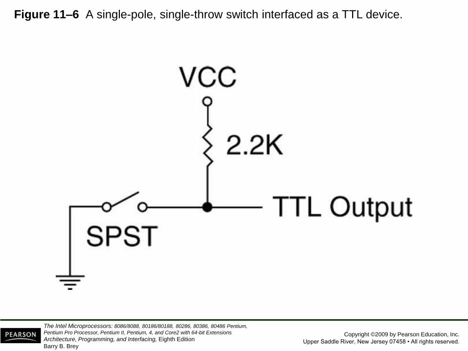
• Fig 11–6 shows a toggle switch properly
connected to function as an input device.
• A pull-up resistor ensures when the switch is
open, the output signal is a logic 1.
– when the switch is closed, it connects to
ground, producing a valid logic 0 level
• A standard range of values for pull-up
resistors is between 1K Ohm and 10K Ohm.
Copyright ©2009 by Pearson Education, Inc.
Upper Saddle River, New Jersey 07458 • All rights reserved.
The Intel Microprocessors: 8086/8088, 80186/80188, 80286, 80386, 80486 Pentium,
Pentium Pro Processor, Pentium II, Pentium, 4, and Core2 with 64-bit Extensions
Architecture, Programming, and Interfacing, Eighth Edition
Barry B. Brey
Figure 11–6 A single-pole, single-throw switch interfaced as a TTL device.

Copyright ©2009 by Pearson Education, Inc.
Upper Saddle River, New Jersey 07458 • All rights reserved.
The Intel Microprocessors: 8086/8088, 80186/80188, 80286, 80386, 80486 Pentium,
Pentium Pro Processor, Pentium II, Pentium, 4, and Core2 with 64-bit Extensions
Architecture, Programming, and Interfacing, Eighth Edition
Barry B. Brey
• Mechanical switch contacts physically bounce
when they are closed,
– which can create a problem if a switch is used
as a clocking signal for a digital circuit
• To prevent problems with bounces, one of the
circuits shown in Fig 11–7 can be used.
– the first is a classic textbook bounce eliminator
– second is a more practical version of the same
• The first version costs more to construct
– the second costs requires no pull-up resistors
and two inverters instead of two NAND gates

Copyright ©2009 by Pearson Education, Inc.
Upper Saddle River, New Jersey 07458 • All rights reserved.
The Intel Microprocessors: 8086/8088, 80186/80188, 80286, 80386, 80486 Pentium,
Pentium Pro Processor, Pentium II, Pentium, 4, and Core2 with 64-bit Extensions
Architecture, Programming, and Interfacing, Eighth Edition
Barry B. Brey
Figure 11–7 Debouncing switch contacts: (a) conventional debouncing and (b)
practical debouncing.
– as the Q input from the switch becomes a logic 0,
it changes the state of the flip-flop
– if the contact bounces away from the Q input, the
flip-flop remembers, no change occurs, and thus
no bounce

Copyright ©2009 by Pearson Education, Inc.
Upper Saddle River, New Jersey 07458 • All rights reserved.
The Intel Microprocessors: 8086/8088, 80186/80188, 80286, 80386, 80486 Pentium,
Pentium Pro Processor, Pentium II, Pentium, 4, and Core2 with 64-bit Extensions
Architecture, Programming, and Interfacing, Eighth Edition
Barry B. Brey
Output Devices
• Output devices are more diverse than input
devices, but many are interfaced in a uniform
manner.
• Before an output device can be interfaced, we
must understand voltages and currents from
the microprocessor or TTL interface.
• Voltages are TTL-compatible from the
microprocessor of the interfacing element.
– logic 0 = 0.0 V to 0.4 V
– logic 1 = 2.4 V to 5.0 V

Copyright ©2009 by Pearson Education, Inc.
Upper Saddle River, New Jersey 07458 • All rights reserved.
The Intel Microprocessors: 8086/8088, 80186/80188, 80286, 80386, 80486 Pentium,
Pentium Pro Processor, Pentium II, Pentium, 4, and Core2 with 64-bit Extensions
Architecture, Programming, and Interfacing, Eighth Edition
Barry B. Brey
• Currents for a processor and many interfacing
components are less than for standard TTL.
– Logic 0 = 0.0 to 2.0 mA
– logic 1 = 0.0 to 400 µA
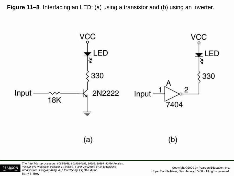
• Fig 11–8 shows how to interface a simple
LED to a microprocessor peripheral pin.
– a transistor driver is used in 11–8(a)
– a TTL inverter is used in 11–8(b)
• The TTL inverter (standard version) provides
up to 16 mA of current at a logic 0 level
– more than enough to drive a standard LED
Copyright ©2009 by Pearson Education, Inc.
Upper Saddle River, New Jersey 07458 • All rights reserved.
The Intel Microprocessors: 8086/8088, 80186/80188, 80286, 80386, 80486 Pentium,
Pentium Pro Processor, Pentium II, Pentium, 4, and Core2 with 64-bit Extensions
Architecture, Programming, and Interfacing, Eighth Edition
Barry B. Brey
Figure 11–8 Interfacing an LED: (a) using a transistor and (b) using an inverter.

Copyright ©2009 by Pearson Education, Inc.
Upper Saddle River, New Jersey 07458 • All rights reserved.
The Intel Microprocessors: 8086/8088, 80186/80188, 80286, 80386, 80486 Pentium,
Pentium Pro Processor, Pentium II, Pentium, 4, and Core2 with 64-bit Extensions
Architecture, Programming, and Interfacing, Eighth Edition
Barry B. Brey
• TTL input signal has minimum value of 2.4 V
• Drop across emitter-base junction is 0.7 V.
• The difference is 1.7 V
– the voltage drop across the resistor
• The value of the resistor is 1.7 V ÷ 0.1 mA or
17K W.
– as 17K W is not a standard value, an 18K W
resistor is chosen

Copyright ©2009 by Pearson Education, Inc.
Upper Saddle River, New Jersey 07458 • All rights reserved.
The Intel Microprocessors: 8086/8088, 80186/80188, 80286, 80386, 80486 Pentium,
Pentium Pro Processor, Pentium II, Pentium, 4, and Core2 with 64-bit Extensions
Architecture, Programming, and Interfacing, Eighth Edition
Barry B. Brey
• In 11–8(a), we elected to use a switching
transistor in place of the TTL buffer.
– 2N2222 is a good low-cost, general-purpose
switching transistor with a minimum gain of 100
– collector current is 10 mA; so base current will
be 1/100 of collector current of 0.1 mA
• To determine the value of the base current–
limiting resistor, use the 0.1 mA base current
and a voltage drop of 1.7 V across the base
current–limiting resistor.

Copyright ©2009 by Pearson Education, Inc.
Upper Saddle River, New Jersey 07458 • All rights reserved.
The Intel Microprocessors: 8086/8088, 80186/80188, 80286, 80386, 80486 Pentium,
Pentium Pro Processor, Pentium II, Pentium, 4, and Core2 with 64-bit Extensions
Architecture, Programming, and Interfacing, Eighth Edition
Barry B. Brey
• Suppose we need to interface a 12 V DC 1A
motor to the microprocessor.
• We cannot use a TTL inverter:
– 12 V signal would burn out the inverter
– current far exceeds 16 mA inverter maximum
• We cannot use a 2N2222 transistor:
– maximum current is 250 mA to 500 mA,
depending on the package style chosen
• The solution is to use a Darlington-pair, such
as a TIP120.
– costs 25¢, can handle 4A current with heat sink

Copyright ©2009 by Pearson Education, Inc.
Upper Saddle River, New Jersey 07458 • All rights reserved.
The Intel Microprocessors: 8086/8088, 80186/80188, 80286, 80386, 80486 Pentium,
Pentium Pro Processor, Pentium II, Pentium, 4, and Core2 with 64-bit Extensions
Architecture, Programming, and Interfacing, Eighth Edition
Barry B. Brey
• Fig 11–9 illustrates a motor connected to the
Darlington-pair with a minimum current gain
of 7000 and a maximum current of 4A.
• Value of the bias resistor is calculated exactly
the same as the one used in the LED driver.
• The current through the resistor is 1.0 A ÷
7000, or about 0.143 mA.
• Voltage drop is 0.9 V because of the two
diode drops (base/emitter junctions).
• The value of the bias resistor is 0.9 V ÷
0.143 mA or 6.29K W.

Copyright ©2009 by Pearson Education, Inc.
Upper Saddle River, New Jersey 07458 • All rights reserved.
The Intel Microprocessors: 8086/8088, 80186/80188, 80286, 80386, 80486 Pentium,
Pentium Pro Processor, Pentium II, Pentium, 4, and Core2 with 64-bit Extensions
Architecture, Programming, and Interfacing, Eighth Edition
Barry B. Brey
Figure 11–9 A DC motor interfaced to a system by using a Darlington-pair.
– The Darlington-pair must use
a heat sink because of the
amount of current
– the diode must be present to
prevent the Darlington-pair
from being destroyed by
inductive kickback

Copyright ©2009 by Pearson Education, Inc.
Upper Saddle River, New Jersey 07458 • All rights reserved.
The Intel Microprocessors: 8086/8088, 80186/80188, 80286, 80386, 80486 Pentium,
Pentium Pro Processor, Pentium II, Pentium, 4, and Core2 with 64-bit Extensions
Architecture, Programming, and Interfacing, Eighth Edition
Barry B. Brey
11–2 I/O PORT ADDRESS
DECODING
• Very similar to memory address decoding,
especially for memory-mapped I/O devices.
• The difference between memory decoding
and isolated I/O decoding is the number of
address pins connected to the decoder.
• In the personal computer system, we always
decode all 16 bits of the I/O port address.

Copyright ©2009 by Pearson Education, Inc.
Upper Saddle River, New Jersey 07458 • All rights reserved.
The Intel Microprocessors: 8086/8088, 80186/80188, 80286, 80386, 80486 Pentium,
Pentium Pro Processor, Pentium II, Pentium, 4, and Core2 with 64-bit Extensions
Architecture, Programming, and Interfacing, Eighth Edition
Barry B. Brey
Decoding 8-Bit I/O Port Addresses
• Fixed I/O instruction uses an 8-bit I/O port
address that on A15–A0 as 0000H–00FFH.
– we often decode only address connections
A7–A0 for an 8-bit I/O port address
• The DX register can also address I/O ports
00H–FFH.
• If the address is decoded as an 8-bit address,
we can never include I/O devices using a 16-
bit address.
– the PC never uses or decodes an 8-bit address

Copyright ©2009 by Pearson Education, Inc.
Upper Saddle River, New Jersey 07458 • All rights reserved.
The Intel Microprocessors: 8086/8088, 80186/80188, 80286, 80386, 80486 Pentium,
Pentium Pro Processor, Pentium II, Pentium, 4, and Core2 with 64-bit Extensions
Architecture, Programming, and Interfacing, Eighth Edition
Barry B. Brey
• Figure 11–10 shows a 74ALS138 decoder
that decodes 8-bit I/O ports F0H - F7H.
– identical to a memory address decoder except
we only connect address bits A7–A0 to the
inputs of the decoder
• Figure 11–11 shows the PLD version, using a
GAL22V10 (a low-cost device) for this
decoder.
• The PLD is a better decoder circuit because
the number of integrated circuits has been
reduced to one device.

Copyright ©2009 by Pearson Education, Inc.
Upper Saddle River, New Jersey 07458 • All rights reserved.
The Intel Microprocessors: 8086/8088, 80186/80188, 80286, 80386, 80486 Pentium,
Pentium Pro Processor, Pentium II, Pentium, 4, and Core2 with 64-bit Extensions
Architecture, Programming, and Interfacing, Eighth Edition
Barry B. Brey
Figure 11–10 A port decoder that decodes 8-bit I/O ports. This decoder generates
active low outputs for ports F0H–F7H.

Copyright ©2009 by Pearson Education, Inc.
Upper Saddle River, New Jersey 07458 • All rights reserved.
The Intel Microprocessors: 8086/8088, 80186/80188, 80286, 80386, 80486 Pentium,
Pentium Pro Processor, Pentium II, Pentium, 4, and Core2 with 64-bit Extensions
Architecture, Programming, and Interfacing, Eighth Edition
Barry B. Brey
Figure 11–11 A PLD that generates part selection signals

Copyright ©2009 by Pearson Education, Inc.
Upper Saddle River, New Jersey 07458 • All rights reserved.
The Intel Microprocessors: 8086/8088, 80186/80188, 80286, 80386, 80486 Pentium,
Pentium Pro Processor, Pentium II, Pentium, 4, and Core2 with 64-bit Extensions
Architecture, Programming, and Interfacing, Eighth Edition
Barry B. Brey
Decoding 16-Bit I/O Port Addresses
• PC systems typically use 16-bit I/O addresses.
– 16-bit addresses rare in embedded systems
• The difference between decoding an 8-bit and
a 16-bit I/O address is that eight additional
address lines (A15–A8) must be decoded.
• Figure 11–12 illustrates a circuit that contains
a PLD and a 4-input NAND gate used to
decode I/O ports EFF8H–EFFFH.
• PLD generates address strobes for I/O ports

Copyright ©2009 by Pearson Education, Inc.
Upper Saddle River, New Jersey 07458 • All rights reserved.
The Intel Microprocessors: 8086/8088, 80186/80188, 80286, 80386, 80486 Pentium,
Pentium Pro Processor, Pentium II, Pentium, 4, and Core2 with 64-bit Extensions
Architecture, Programming, and Interfacing, Eighth Edition
Barry B. Brey
Figure 11–12 A PLD that decodes 16-bit I/O ports EFF8H through EFFFH.

Copyright ©2009 by Pearson Education, Inc.
Upper Saddle River, New Jersey 07458 • All rights reserved.
The Intel Microprocessors: 8086/8088, 80186/80188, 80286, 80386, 80486 Pentium,
Pentium Pro Processor, Pentium II, Pentium, 4, and Core2 with 64-bit Extensions
Architecture, Programming, and Interfacing, Eighth Edition
Barry B. Brey
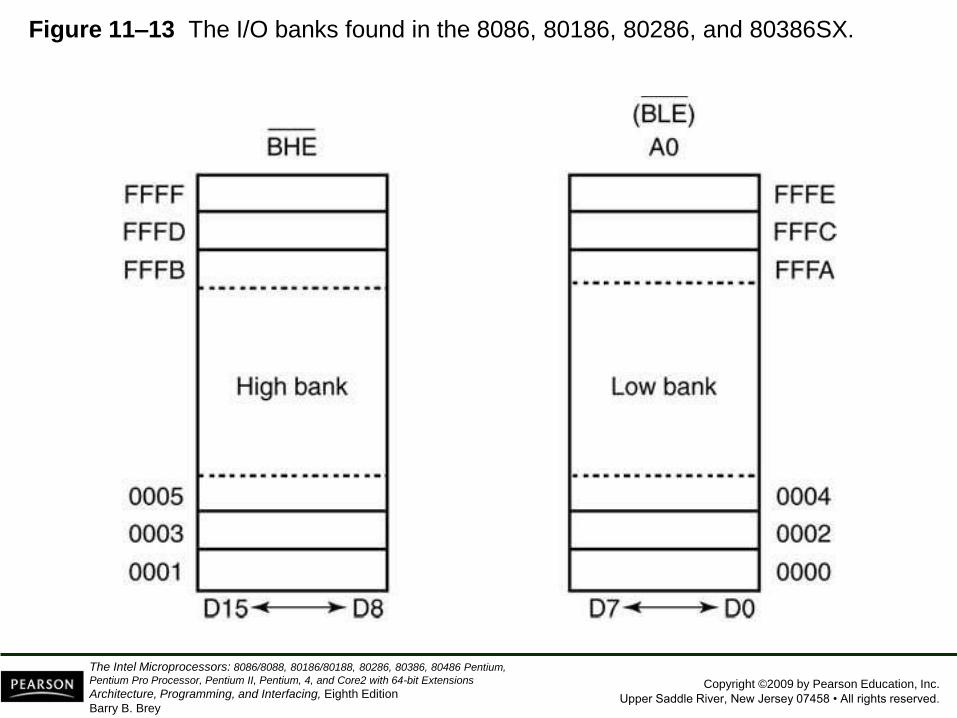
8- and 16-Bit Wide I/O Ports
• Data transferred to an 8-bit I/O device exist in
one of the I/O banks in a 16-bit processor
such as 80386SX.
• The I/O system on such a microprocessor
contains two 8-bit memory banks.
• Fig 11–13 shows separate I/O banks for a
16-bit system such as 80386SX.
• Because two I/O banks exist, any 8-bit I/O
write requires a separate write.
Copyright ©2009 by Pearson Education, Inc.
Upper Saddle River, New Jersey 07458 • All rights reserved.
The Intel Microprocessors: 8086/8088, 80186/80188, 80286, 80386, 80486 Pentium,
Pentium Pro Processor, Pentium II, Pentium, 4, and Core2 with 64-bit Extensions
Architecture, Programming, and Interfacing, Eighth Edition
Barry B. Brey
Figure 11–13 The I/O banks found in the 8086, 80186, 80286, and 80386SX.

Copyright ©2009 by Pearson Education, Inc.
Upper Saddle River, New Jersey 07458 • All rights reserved.
The Intel Microprocessors: 8086/8088, 80186/80188, 80286, 80386, 80486 Pentium,
Pentium Pro Processor, Pentium II, Pentium, 4, and Core2 with 64-bit Extensions
Architecture, Programming, and Interfacing, Eighth Edition
Barry B. Brey
• I/O reads don’t require separate strobes.
– as with memory, the processor reads only the
byte it expects and ignores the other byte
– a read can cause problems when an I/O device
responds incorrectly to a read operation
• Fig 11–14 showss a system with two different
8-bit output devices, located at 40H and 41H.
• These are 8-bit devices and appear in
different I/O banks.
– thus, separate I/O write signals are generated to
clock a pair of latches that capture port data

Copyright ©2009 by Pearson Education, Inc.
Upper Saddle River, New Jersey 07458 • All rights reserved.
The Intel Microprocessors: 8086/8088, 80186/80188, 80286, 80386, 80486 Pentium,
Pentium Pro Processor, Pentium II, Pentium, 4, and Core2 with 64-bit Extensions
Architecture, Programming, and Interfacing, Eighth Edition
Barry B. Brey
Figure 11–14 An I/O port decoder that selects ports 40H and 41H for output data.
– all I/O ports
use 8-bit
addresses
– ports 40H &
41H can be
addressed
as separate
8-bit ports
– or as one
16-bit port

Copyright ©2009 by Pearson Education, Inc.
Upper Saddle River, New Jersey 07458 • All rights reserved.
The Intel Microprocessors: 8086/8088, 80186/80188, 80286, 80386, 80486 Pentium,
Pentium Pro Processor, Pentium II, Pentium, 4, and Core2 with 64-bit Extensions
Architecture, Programming, and Interfacing, Eighth Edition
Barry B. Brey
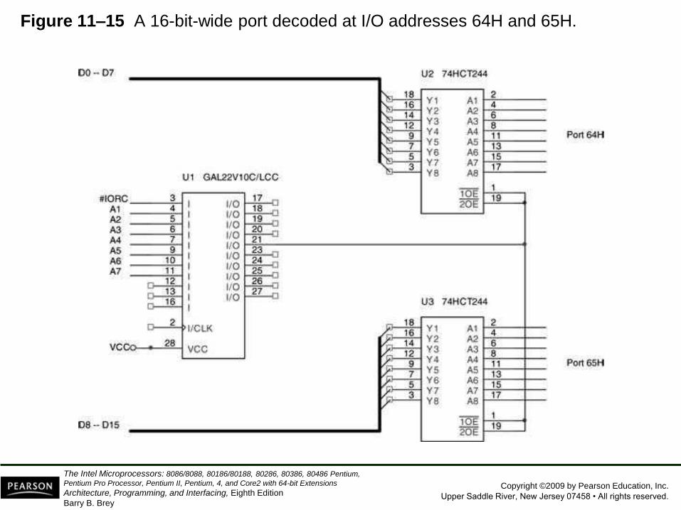
• Fig 11–15 shows a 16-bit device connected
to function at 8-bit addresses 64H & 65H.
• The PLD decoder does not have a connection
for address bits BLE (A0) and BHE because
the signals don’t apply to 16-bit-wide devices.
• The program for the PLD, illustrated in
Example 11–5, shows how the enable
signals are generated for the three-state
buffers (74HCT244) used as input devices.
Copyright ©2009 by Pearson Education, Inc.
Upper Saddle River, New Jersey 07458 • All rights reserved.
The Intel Microprocessors: 8086/8088, 80186/80188, 80286, 80386, 80486 Pentium,
Pentium Pro Processor, Pentium II, Pentium, 4, and Core2 with 64-bit Extensions
Architecture, Programming, and Interfacing, Eighth Edition
Barry B. Brey
Figure 11–15 A 16-bit-wide port decoded at I/O addresses 64H and 65H.

Copyright ©2009 by Pearson Education, Inc.
Upper Saddle River, New Jersey 07458 • All rights reserved.
The Intel Microprocessors: 8086/8088, 80186/80188, 80286, 80386, 80486 Pentium,
Pentium Pro Processor, Pentium II, Pentium, 4, and Core2 with 64-bit Extensions
Architecture, Programming, and Interfacing, Eighth Edition
Barry B. Brey
32-Bit-Wide I/O Ports
• May eventually become common because of
newer buses found in computer systems.
• The EISA system bus supports 32-bit I/O as
well as the VESA local and current PCI bus.
– not many I/O devices are 32 bits in width
• Fig 11–16 shows a 32-bit input port for
80386DX - 80486DX microprocessor.
• The circuit uses a single PLD to decode the
I/O ports and four 74HCT244 buffers to
connect the I/O data to the data bus.

Copyright ©2009 by Pearson Education, Inc.
Upper Saddle River, New Jersey 07458 • All rights reserved.
The Intel Microprocessors: 8086/8088, 80186/80188, 80286, 80386, 80486 Pentium,
Pentium Pro Processor, Pentium II, Pentium, 4, and Core2 with 64-bit Extensions
Architecture, Programming, and Interfacing, Eighth Edition
Barry B. Brey
Figure 11–16 A 32-bit-wide port decoded at 70H through 73H for the 80486DX
microprocessor.
– I/O ports decoded
by this interface
are the 8-bit ports
70H–73H
– When writing to
access this port,
it is crucial to use
the address 70H
for 32-bit input
– as instruction
IN EAX, 70H

Copyright ©2009 by Pearson Education, Inc.
Upper Saddle River, New Jersey 07458 • All rights reserved.
The Intel Microprocessors: 8086/8088, 80186/80188, 80286, 80386, 80486 Pentium,
Pentium Pro Processor, Pentium II, Pentium, 4, and Core2 with 64-bit Extensions
Architecture, Programming, and Interfacing, Eighth Edition
Barry B. Brey
• With the Pentium–Core2 and their 64-bit data
buses, I/O ports appear in various banks, as
determined by the I/O port address.
• A 32-bit I/O access in the Pentium system
can appear in any four consecutive I/O banks.
– 32-bit ports 0100H–0103H appear in banks 0–3
• I/O address range must begin at a location
where the rightmost two bits are zeros.
– 0100H–0103H is allowable
– 0101H–0104H is not

Copyright ©2009 by Pearson Education, Inc.
Upper Saddle River, New Jersey 07458 • All rights reserved.
The Intel Microprocessors: 8086/8088, 80186/80188, 80286, 80386, 80486 Pentium,
Pentium Pro Processor, Pentium II, Pentium, 4, and Core2 with 64-bit Extensions
Architecture, Programming, and Interfacing, Eighth Edition
Barry B. Brey
• Widest I/O transfers are 32 bits, and there are
no I/O instructions to support 64-bit transfers.
– true for Pentium 4 or Core2 in the 64-bit mode
• Suppose we need to interface a 16-bit-wide
output port at I/O address 2000H and 2001H.
– interface is illustrated in Figure 11–17
– PLD program is listed in Example 11–7
• The problem that can arise is when the I/O
port spans across a 64-bit boundary.
– example, a 16-bit- port at 2007H and 2008H

Copyright ©2009 by Pearson Education, Inc.
Upper Saddle River, New Jersey 07458 • All rights reserved.
The Intel Microprocessors: 8086/8088, 80186/80188, 80286, 80386, 80486 Pentium,
Pentium Pro Processor, Pentium II, Pentium, 4, and Core2 with 64-bit Extensions
Architecture, Programming, and Interfacing, Eighth Edition
Barry B. Brey
Figure 11–17 A Pentium 4 interfaced to a 16-bit-wide I/O port at port addresses
2000H and 2001H.

Copyright ©2009 by Pearson Education, Inc.
Upper Saddle River, New Jersey 07458 • All rights reserved.
The Intel Microprocessors: 8086/8088, 80186/80188, 80286, 80386, 80486 Pentium,
Pentium Pro Processor, Pentium II, Pentium, 4, and Core2 with 64-bit Extensions
Architecture, Programming, and Interfacing, Eighth Edition
Barry B. Brey
11–3 THE PROGRAMMABLE
PERIPHERAL
• 82C55 programmable peripheral interface
(PPI) is a popular, low-cost interface
component found in many applications.
• The PPI has 24 pins for I/O, programmable in
groups of 12 pins and groups that operate in
three distinct modes of operation.
• 82C55 can interface any TTL-compatible
I/O device to the microprocessor.
Copyright ©2009 by Pearson Education, Inc.
Upper Saddle River, New Jersey 07458 • All rights reserved.
The Intel Microprocessors: 8086/8088, 80186/80188, 80286, 80386, 80486 Pentium,
Pentium Pro Processor, Pentium II, Pentium, 4, and Core2 with 64-bit Extensions
Architecture, Programming, and Interfacing, Eighth Edition
Barry B. Brey
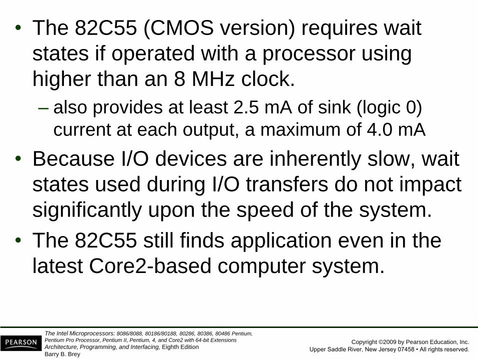
• The 82C55 (CMOS version) requires wait
states if operated with a processor using
higher than an 8 MHz clock.
– also provides at least 2.5 mA of sink (logic 0)
current at each output, a maximum of 4.0 mA
• Because I/O devices are inherently slow, wait
states used during I/O transfers do not impact
significantly upon the speed of the system.
• The 82C55 still finds application even in the
latest Core2-based computer system.
Copyright ©2009 by Pearson Education, Inc.
Upper Saddle River, New Jersey 07458 • All rights reserved.
The Intel Microprocessors: 8086/8088, 80186/80188, 80286, 80386, 80486 Pentium,
Pentium Pro Processor, Pentium II, Pentium, 4, and Core2 with 64-bit Extensions
Architecture, Programming, and Interfacing, Eighth Edition
Barry B. Brey
• 82C55 is used for interface to the keyboard
and parallel printer port in many PCs.
– found as a function within an interfacing chip set
– also controls the timer and reads data from the
keyboard interface
• An experimentation board is available that
plugs into the parallel port of a PC, to allow
access to an 8255 located on the board.
• The 8255 is programmed in either assembly
language or Visual C++ through drivers
available with the board.

Copyright ©2009 by Pearson Education, Inc.
Upper Saddle River, New Jersey 07458 • All rights reserved.
The Intel Microprocessors: 8086/8088, 80186/80188, 80286, 80386, 80486 Pentium,
Pentium Pro Processor, Pentium II, Pentium, 4, and Core2 with 64-bit Extensions
Architecture, Programming, and Interfacing, Eighth Edition
Barry B. Brey
Basic Description of the 82C55
• Fig 11–18 shows pin-outs of the 82C55 in
DIP and surface mount (flat pack) format.
• The three I/O ports (labeled A, B, and C) are
programmed as groups.
– group A connections consist of port A (PA7–PA0)
and the upper half of port C (PC7–PC4)
– group B consists of port B (PB7–PB0) and the
lower half of port C (PC3–PC0)
• 82C55 is selected by its CS pin for
programming and reading/writing to a port.

Copyright ©2009 by Pearson Education, Inc.
Upper Saddle River, New Jersey 07458 • All rights reserved.
The Intel Microprocessors: 8086/8088, 80186/80188, 80286, 80386, 80486 Pentium,
Pentium Pro Processor, Pentium II, Pentium, 4, and Core2 with 64-bit Extensions
Architecture, Programming, and Interfacing, Eighth Edition
Barry B. Brey
Figure 11–18 The pin-out of the 82C55 peripheral interface adapter (PPI).
Copyright ©2009 by Pearson Education, Inc.
Upper Saddle River, New Jersey 07458 • All rights reserved.
The Intel Microprocessors: 8086/8088, 80186/80188, 80286, 80386, 80486 Pentium,
Pentium Pro Processor, Pentium II, Pentium, 4, and Core2 with 64-bit Extensions
Architecture, Programming, and Interfacing, Eighth Edition
Barry B. Brey
• Table 11–2 shows I/O port assignments used
for programming and access to the I/O ports.
• In the PC, a pair of 82C55s, or equivalents,
are decoded at I/O ports 60H–63H and also
at ports 378H–37BH.
• The 82C55 is a fairly simple device to
interface to the microprocessor and program.
• For 82C55 to be read or written, the CS input
must be logic 0 and the correct I/O address
must be applied to the A1 and A0 pins.
• Remaining port address pins are don’t cares.

Copyright ©2009 by Pearson Education, Inc.
Upper Saddle River, New Jersey 07458 • All rights reserved.
The Intel Microprocessors: 8086/8088, 80186/80188, 80286, 80386, 80486 Pentium,
Pentium Pro Processor, Pentium II, Pentium, 4, and Core2 with 64-bit Extensions
Architecture, Programming, and Interfacing, Eighth Edition
Barry B. Brey
• Fig 11–19 shows an 82C55 connected to the
80386SX so it functions at 8-bit addresses
C0H (port A), C2H (port B), C4H (port C),
and C6H (command register).
– this interface uses the low bank of the I/O map
• All 82C55 pins are direct connections to the
80386SX, except the CS pin. The pin is
decoded/selected by a 74ALS138 decoder.
• A RESET to 82C55 sets up all ports as
simple input ports using mode 0 operation.
– initializes the device when the processor is reset

Copyright ©2009 by Pearson Education, Inc.
Upper Saddle River, New Jersey 07458 • All rights reserved.
The Intel Microprocessors: 8086/8088, 80186/80188, 80286, 80386, 80486 Pentium,
Pentium Pro Processor, Pentium II, Pentium, 4, and Core2 with 64-bit Extensions
Architecture, Programming, and Interfacing, Eighth Edition
Barry B. Brey
Figure 11–19 The 82C55 interfaced to the low bank of the 80386SX microprocessor.

Copyright ©2009 by Pearson Education, Inc.
Upper Saddle River, New Jersey 07458 • All rights reserved.
The Intel Microprocessors: 8086/8088, 80186/80188, 80286, 80386, 80486 Pentium,
Pentium Pro Processor, Pentium II, Pentium, 4, and Core2 with 64-bit Extensions
Architecture, Programming, and Interfacing, Eighth Edition
Barry B. Brey
• After a RESET, no other commands are
needed, as long as it is used as an input
device for all three ports.
• 82C55 is interfaced to the PC at port
addresses 60H–63H for keyboard control.
– also for controlling the speaker, timer, and other
internal devices such as memory expansion
• It is also used for the parallel printer port at
I/O ports 378H–37BH.

Copyright ©2009 by Pearson Education, Inc.
Upper Saddle River, New Jersey 07458 • All rights reserved.
The Intel Microprocessors: 8086/8088, 80186/80188, 80286, 80386, 80486 Pentium,
Pentium Pro Processor, Pentium II, Pentium, 4, and Core2 with 64-bit Extensions
Architecture, Programming, and Interfacing, Eighth Edition
Barry B. Brey
Programming the 82C55
• 82C55 is programmed through two internal
command registers shown in Figure 11–20.
• Bit position 7 selects either command byte A
or command byte B.
– command byte A programs functions of group
A and B
– byte B sets (1) or resets (0) bits of port C only
if the 82C55 is programmed in mode 1 or 2
• Group B (port B and the lower part of port C)
are programmed as input or output pins.

Copyright ©2009 by Pearson Education, Inc.
Upper Saddle River, New Jersey 07458 • All rights reserved.
The Intel Microprocessors: 8086/8088, 80186/80188, 80286, 80386, 80486 Pentium,
Pentium Pro Processor, Pentium II, Pentium, 4, and Core2 with 64-bit Extensions
Architecture, Programming, and Interfacing, Eighth Edition
Barry B. Brey
Figure 11–20 The command byte of the command register in the 82C55. (a)
Programs ports A, B, and C. (b) Sets or resets the bit indicated in the select a bit field.
– group B operates in mode 0 or
mode 1
– mode 0 is basic input/output mode
that allows the pins of group B to
be programmed as simple input
and latched output connections
– Mode 1 operation is the strobed
operation for group B connections
– data are transferred through port B
– handshaking signals are provided
by port C

Copyright ©2009 by Pearson Education, Inc.
Upper Saddle River, New Jersey 07458 • All rights reserved.
The Intel Microprocessors: 8086/8088, 80186/80188, 80286, 80386, 80486 Pentium,
Pentium Pro Processor, Pentium II, Pentium, 4, and Core2 with 64-bit Extensions
Architecture, Programming, and Interfacing, Eighth Edition
Barry B. Brey
• Group A (port A and the upper part of port C)
are programmed as input or output pins.
• Group A can operate in modes 0, 1, and 2.
– mode 2 operation is a bidirectional mode of
operation for port A
• If a 0 is placed in bit position 7 of the
command byte, command byte B is selected
• This allows any bit of port C to be set (1) or
reset (0), if the 82C55 is operated in either
mode 1 or 2.
– otherwise, this byte is not used for programming
Copyright ©2009 by Pearson Education, Inc.
Upper Saddle River, New Jersey 07458 • All rights reserved.
The Intel Microprocessors: 8086/8088, 80186/80188, 80286, 80386, 80486 Pentium,
Pentium Pro Processor, Pentium II, Pentium, 4, and Core2 with 64-bit Extensions
Architecture, Programming, and Interfacing, Eighth Edition
Barry B. Brey
Mode 0 Operation
• Mode 0 operation causes 82C55 to function:
– as a buffered input device
– as a latched output device
• Fig 11–21 shows 82C55 connected to a
set of eight seven-segment LED displays.
• These are standard LEDs.
– the interface can be modified with a change
in resistor values for an organic LED (OLED)
display or high-brightness LEDs

Copyright ©2009 by Pearson Education, Inc.
Upper Saddle River, New Jersey 07458 • All rights reserved.
The Intel Microprocessors: 8086/8088, 80186/80188, 80286, 80386, 80486 Pentium,
Pentium Pro Processor, Pentium II, Pentium, 4, and Core2 with 64-bit Extensions
Architecture, Programming, and Interfacing, Eighth Edition
Barry B. Brey
Figure 11–21 An 8-digit LED display interfaced to the 8088 microprocessor through
an 82C55 PIA.
– ports A & B are programmed as
(mode 0) simple latched output ports
– port A provides segment data inputs
port B provides a means of selecting
one display position at a time for
multiplexing the displays
– the 82C55 is interfaced to an 8088
through a PLD so it functions at
I/O port numbers 0700H–0703H
– PLD decodes the I/O address and
develops the write strobe for the WR
pin of the 82C55
Copyright ©2009 by Pearson Education, Inc.
Upper Saddle River, New Jersey 07458 • All rights reserved.
The Intel Microprocessors: 8086/8088, 80186/80188, 80286, 80386, 80486 Pentium,
Pentium Pro Processor, Pentium II, Pentium, 4, and Core2 with 64-bit Extensions
Architecture, Programming, and Interfacing, Eighth Edition
Barry B. Brey
• Resistor values in Fig 11–21 are chosen so
the segment current is 80 mA.
– required to produce average 10 mA current
per segment as the displays are multiplexed
• A six-digit display uses a segment current of
60 mA for an average of 10 mA per segment.
• Peak anode current in an eight-digit display
is 560 mA (seven segments 80 mA).
– average anode current is 80 mA
• In a six-digit display, peak current would be
420 mA (seven segments 60 mA).

Copyright ©2009 by Pearson Education, Inc.
Upper Saddle River, New Jersey 07458 • All rights reserved.
The Intel Microprocessors: 8086/8088, 80186/80188, 80286, 80386, 80486 Pentium,
Pentium Pro Processor, Pentium II, Pentium, 4, and Core2 with 64-bit Extensions
Architecture, Programming, and Interfacing, Eighth Edition
Barry B. Brey
• In this display, the segment load resistor
passes 80 mA current and has approximately
3.0 V across it.
• The value of the resistor is 3.0 V ÷ 180 mA =
37.5 Ohm. The closest standard resistor
value of 39 Ohm is used in Fig11–21.
• Programming the 82C55 is accomplished by
the short sequence of instructions listed in
Example 11–9.
• Ports A and B are programmed as outputs.
Copyright ©2009 by Pearson Education, Inc.
Upper Saddle River, New Jersey 07458 • All rights reserved.
The Intel Microprocessors: 8086/8088, 80186/80188, 80286, 80386, 80486 Pentium,
Pentium Pro Processor, Pentium II, Pentium, 4, and Core2 with 64-bit Extensions
Architecture, Programming, and Interfacing, Eighth Edition
Barry B. Brey
An LCD Display Interfaced to the
82C55
• LCDs (liquid crystal displays) have replaced
LED displays in many applications.
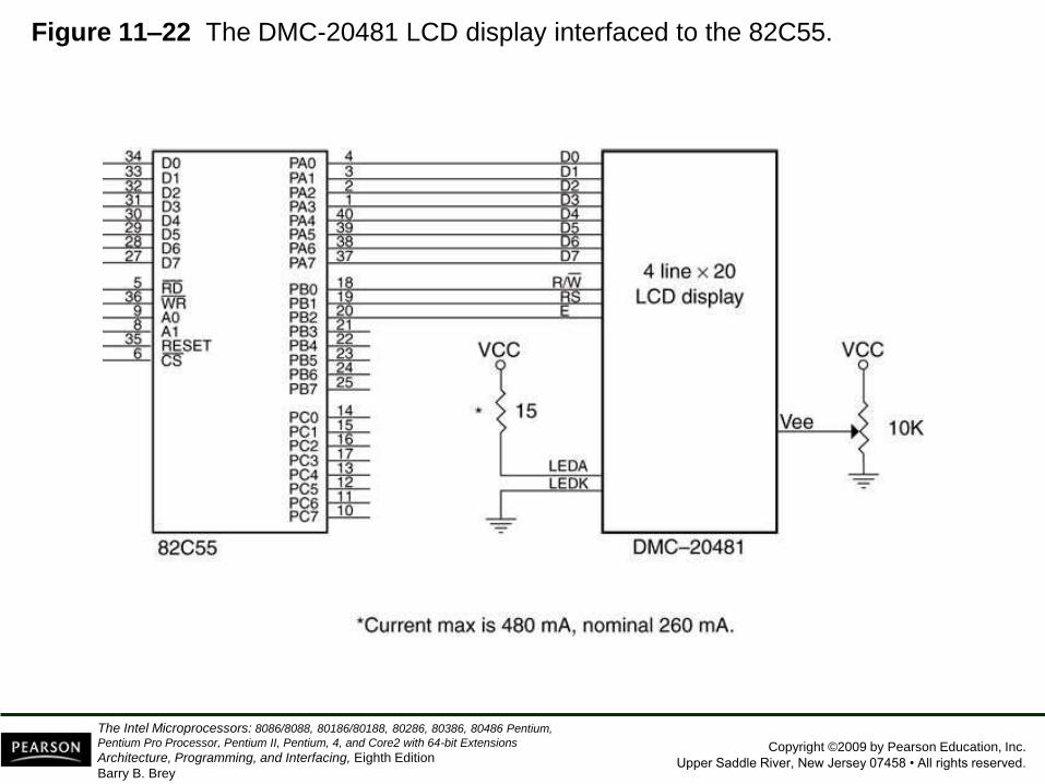
• Fig 11–22 shows an Optrex DMC-20481 LCD
display interfaced to an 82C55.
– DMC-20481 is a 4-line by 20-characters-per-line
display that accepts ASCII code as input data
• It also accepts commands that initialize it and
control its application.
Copyright ©2009 by Pearson Education, Inc.
Upper Saddle River, New Jersey 07458 • All rights reserved.
The Intel Microprocessors: 8086/8088, 80186/80188, 80286, 80386, 80486 Pentium,
Pentium Pro Processor, Pentium II, Pentium, 4, and Core2 with 64-bit Extensions
Architecture, Programming, and Interfacing, Eighth Edition
Barry B. Brey
Figure 11–22 The DMC-20481 LCD display interfaced to the 82C55.

Copyright ©2009 by Pearson Education, Inc.
Upper Saddle River, New Jersey 07458 • All rights reserved.
The Intel Microprocessors: 8086/8088, 80186/80188, 80286, 80386, 80486 Pentium,
Pentium Pro Processor, Pentium II, Pentium, 4, and Core2 with 64-bit Extensions
Architecture, Programming, and Interfacing, Eighth Edition
Barry B. Brey
• The data connections, which are attached to
the 82C55 port A, are used to input display
data and to read information from the display.
• For a 4-bit interface, D4–D7 pins are used
where the data must be formatted with the
high nibble first, followed by the low nibble.
• A few newer OLED devices contain a serial
interface that uses a single pin for the data.
Copyright ©2009 by Pearson Education, Inc.
Upper Saddle River, New Jersey 07458 • All rights reserved.
The Intel Microprocessors: 8086/8088, 80186/80188, 80286, 80386, 80486 Pentium,
Pentium Pro Processor, Pentium II, Pentium, 4, and Core2 with 64-bit Extensions
Architecture, Programming, and Interfacing, Eighth Edition
Barry B. Brey
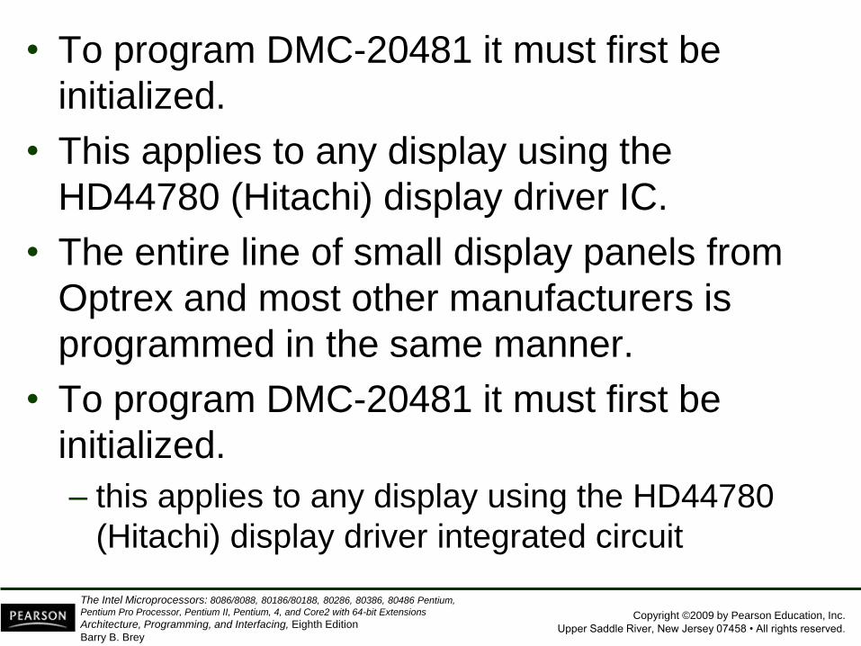
• To program DMC-20481 it must first be
initialized.
• This applies to any display using the
HD44780 (Hitachi) display driver IC.
• The entire line of small display panels from
Optrex and most other manufacturers is
programmed in the same manner.
• To program DMC-20481 it must first be
initialized.
– this applies to any display using the HD44780
(Hitachi) display driver integrated circuit

Copyright ©2009 by Pearson Education, Inc.
Upper Saddle River, New Jersey 07458 • All rights reserved.
The Intel Microprocessors: 8086/8088, 80186/80188, 80286, 80386, 80486 Pentium,
Pentium Pro Processor, Pentium II, Pentium, 4, and Core2 with 64-bit Extensions
Architecture, Programming, and Interfacing, Eighth Edition
Barry B. Brey
• Initialization is accomplished via the following:
– 1. Wait at least 15 ms after VCC rises to 5.0 V
– 2. Output the function set command (30H), and
wait at least 4.1 ms
– 3. Output the function set command (30H) a
second time, and wait at least 100 µs
– 4. Output the function set command (30H) a
third time, and wait at least 40 µs
– 5. Output the function set command (38H) a
fourth time, and wait at least 40 µs
– 6. Output 08H to disable the display, and wait
at least 40 µs
Copyright ©2009 by Pearson Education, Inc.
Upper Saddle River, New Jersey 07458 • All rights reserved.
The Intel Microprocessors: 8086/8088, 80186/80188, 80286, 80386, 80486 Pentium,
Pentium Pro Processor, Pentium II, Pentium, 4, and Core2 with 64-bit Extensions
Architecture, Programming, and Interfacing, Eighth Edition
Barry B. Brey
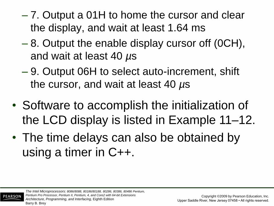
– 7. Output a 01H to home the cursor and clear
the display, and wait at least 1.64 ms
– 8. Output the enable display cursor off (0CH),
and wait at least 40 µs
– 9. Output 06H to select auto-increment, shift
the cursor, and wait at least 40 µs
• Software to accomplish the initialization of
the LCD display is listed in Example 11–12.
• The time delays can also be obtained by
using a timer in C++.

Copyright ©2009 by Pearson Education, Inc.
Upper Saddle River, New Jersey 07458 • All rights reserved.
The Intel Microprocessors: 8086/8088, 80186/80188, 80286, 80386, 80486 Pentium,
Pentium Pro Processor, Pentium II, Pentium, 4, and Core2 with 64-bit Extensions
Architecture, Programming, and Interfacing, Eighth Edition
Barry B. Brey
• After initialization, time delays are no longer
needed when sending data or many
commands to the display.
• The clear display command still needs a time
delay as the busy flag is not used .
• Instead of a time delay, the busy flag is tested
to see whether the display has completed an
operation.
• The BUSY procedure tests the LCD display
and only returns when the display has
completed a prior instruction.

Copyright ©2009 by Pearson Education, Inc.
Upper Saddle River, New Jersey 07458 • All rights reserved.
The Intel Microprocessors: 8086/8088, 80186/80188, 80286, 80386, 80486 Pentium,
Pentium Pro Processor, Pentium II, Pentium, 4, and Core2 with 64-bit Extensions
Architecture, Programming, and Interfacing, Eighth Edition
Barry B. Brey
• Once the BUSY procedure is available, data
can be sent to the display by writing another
procedure called WRITE.
• The WRITE procedure uses BUSY to test
before trying to write new data to the display.
• Example 11–14 shows the WRITE procedure,
which transfers the ASCII character from the
BL register to the current cursor position of
the display.

Copyright ©2009 by Pearson Education, Inc.
Upper Saddle River, New Jersey 07458 • All rights reserved.
The Intel Microprocessors: 8086/8088, 80186/80188, 80286, 80386, 80486 Pentium,
Pentium Pro Processor, Pentium II, Pentium, 4, and Core2 with 64-bit Extensions
Architecture, Programming, and Interfacing, Eighth Edition
Barry B. Brey
• The only other procedure needed for a basic
display is the clear & home cursor procedure,
called CLS, shown in Example 11–15.
• This procedure uses the SEND macro from
the initialization software to send the clear
command to the display.
• With CLS and the procedures presented thus
far, you can display any message on the
display, clear it, display another message,
and basically operate the display.

Copyright ©2009 by Pearson Education, Inc.
Upper Saddle River, New Jersey 07458 • All rights reserved.
The Intel Microprocessors: 8086/8088, 80186/80188, 80286, 80386, 80486 Pentium,
Pentium Pro Processor, Pentium II, Pentium, 4, and Core2 with 64-bit Extensions
Architecture, Programming, and Interfacing, Eighth Edition
Barry B. Brey
A Stepper Motor Interfaced to the
82C55.
• Another device often interfaced to a computer
system is the stepper motor.
– a digital motor because it is moved in discrete
steps as it traverses through 360°
• An inexpensive stepper motor is geared to
move perhaps 15° per step
• A more costly, high-precision stepper motor
can be geared to 1° per step.
Copyright ©2009 by Pearson Education, Inc.
Upper Saddle River, New Jersey 07458 • All rights reserved.
The Intel Microprocessors: 8086/8088, 80186/80188, 80286, 80386, 80486 Pentium,
Pentium Pro Processor, Pentium II, Pentium, 4, and Core2 with 64-bit Extensions
Architecture, Programming, and Interfacing, Eighth Edition
Barry B. Brey
• In all cases, these steps are gained through
many magnetic poles and/or gearing.
• Figure 11–23 shows a four-coil stepper motor
that uses an armature with a single pole.
– two coils are energized
• If less power is required, one coil may be
energized at a time, causing the motor to
step at 45°, 135°, 225°, and 315°.
• The motor is shown with the armature rotated
to four discrete places, called full stepping.
– accomplished by energizing the coils, as shown

Copyright ©2009 by Pearson Education, Inc.
Upper Saddle River, New Jersey 07458 • All rights reserved.
The Intel Microprocessors: 8086/8088, 80186/80188, 80286, 80386, 80486 Pentium,
Pentium Pro Processor, Pentium II, Pentium, 4, and Core2 with 64-bit Extensions
Architecture, Programming, and Interfacing, Eighth Edition
Barry B. Brey
Figure 11–23 The stepper motor showing full-step operation: (a) 45° (b) 135° (c)
225° (d) 315°.

Copyright ©2009 by Pearson Education, Inc.
Upper Saddle River, New Jersey 07458 • All rights reserved.
The Intel Microprocessors: 8086/8088, 80186/80188, 80286, 80386, 80486 Pentium,
Pentium Pro Processor, Pentium II, Pentium, 4, and Core2 with 64-bit Extensions
Architecture, Programming, and Interfacing, Eighth Edition
Barry B. Brey
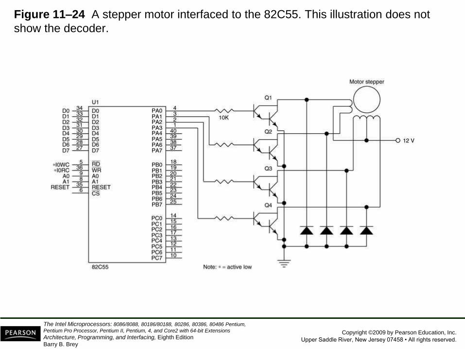
• The motor is driven by NPN Darlington amp
pairs to provide a large current to each coil.
• A circuit that can drive this stepper motor is
illustrated in Fig 11–24.
– with the four coils shown in place
• This circuit uses the 82C55 to provide drive
signals used to rotate the motor armature in
either the right- or left-hand direction.
• A simple procedure that drives the motor is
listed in Example 11–16 in both assembly
language and as a function in C++.
Copyright ©2009 by Pearson Education, Inc.
Upper Saddle River, New Jersey 07458 • All rights reserved.
The Intel Microprocessors: 8086/8088, 80186/80188, 80286, 80386, 80486 Pentium,
Pentium Pro Processor, Pentium II, Pentium, 4, and Core2 with 64-bit Extensions
Architecture, Programming, and Interfacing, Eighth Edition
Barry B. Brey
Figure 11–24 A stepper motor interfaced to the 82C55. This illustration does not
show the decoder.

Copyright ©2009 by Pearson Education, Inc.
Upper Saddle River, New Jersey 07458 • All rights reserved.
The Intel Microprocessors: 8086/8088, 80186/80188, 80286, 80386, 80486 Pentium,
Pentium Pro Processor, Pentium II, Pentium, 4, and Core2 with 64-bit Extensions
Architecture, Programming, and Interfacing, Eighth Edition
Barry B. Brey
Key Matrix Interface
• Keyboards come in a variety of sizes, from
standard 101-key QWERTY keyboards to
special keyboards that contain 4 to 16 keys.
• Fig 11–25 is a key matrix with 16 switches
interfaced to ports A and B of an 82C55.
– the switches are formed into a 4 4 matrix,
but any matrix could be used, such as a 2 8
• The keys are organized into four rows and
columns: (ROW0–ROW3) (COL0–COL3)

Copyright ©2009 by Pearson Education, Inc.
Upper Saddle River, New Jersey 07458 • All rights reserved.
The Intel Microprocessors: 8086/8088, 80186/80188, 80286, 80386, 80486 Pentium,
Pentium Pro Processor, Pentium II, Pentium, 4, and Core2 with 64-bit Extensions
Architecture, Programming, and Interfacing, Eighth Edition
Barry B. Brey
Figure 11–25 A 4 4 keyboard matrix connected to an 8088 microprocessor through
the 82C55 PIA.
– the 82C55 is decoded at I/O
ports 50H–53H for an 8088
– port A is programmed as an
input port to read the rows
– port B is programmed as an
output port to select a column
– a flowchart of the software
required to read a key from the
keyboard matrix and debounce
the key is illustrated in Fig 11–26
Copyright ©2009 by Pearson Education, Inc.
Upper Saddle River, New Jersey 07458 • All rights reserved.
The Intel Microprocessors: 8086/8088, 80186/80188, 80286, 80386, 80486 Pentium,
Pentium Pro Processor, Pentium II, Pentium, 4, and Core2 with 64-bit Extensions
Architecture, Programming, and Interfacing, Eighth Edition
Barry B. Brey
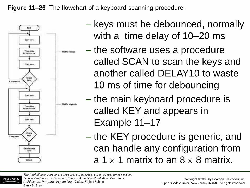
Figure 11–26 The flowchart of a keyboard-scanning procedure.
– keys must be debounced, normally
with a time delay of 10–20 ms
– the software uses a procedure
called SCAN to scan the keys and
another called DELAY10 to waste
10 ms of time for debouncing
– the main keyboard procedure is
called KEY and appears in
Example 11–17
– the KEY procedure is generic, and
can handle any configuration from
a 1 1 matrix to an 8 8 matrix.

Copyright ©2009 by Pearson Education, Inc.
Upper Saddle River, New Jersey 07458 • All rights reserved.
The Intel Microprocessors: 8086/8088, 80186/80188, 80286, 80386, 80486 Pentium,
Pentium Pro Processor, Pentium II, Pentium, 4, and Core2 with 64-bit Extensions
Architecture, Programming, and Interfacing, Eighth Edition
Barry B. Brey
• The ShortDelay procedure is needed as the
computer changes port B at a very high rate .
– the time delay allows the data sent to port B to
settle to their final state
• This is not needed if scan rate (time between
output instructions) does not exceed 30 KHz.
– if the scanning frequency is higher, the device
generates radio interference
• If so, the FCC will not approve application
in any accepted system
– without certification the system cannot be sold

Copyright ©2009 by Pearson Education, Inc.
Upper Saddle River, New Jersey 07458 • All rights reserved.
The Intel Microprocessors: 8086/8088, 80186/80188, 80286, 80386, 80486 Pentium,
Pentium Pro Processor, Pentium II, Pentium, 4, and Core2 with 64-bit Extensions
Architecture, Programming, and Interfacing, Eighth Edition
Barry B. Brey
Mode 1 Strobed Input
• Causes port A and/or port B to function as
latching input devices.
– allows external data to be stored to the port
until the microprocessor is ready to retrieve it
• Port C is used in mode 1 operation—not for
data, but for control or handshaking signals.
– to help operate either or both port A and B as
strobed input ports
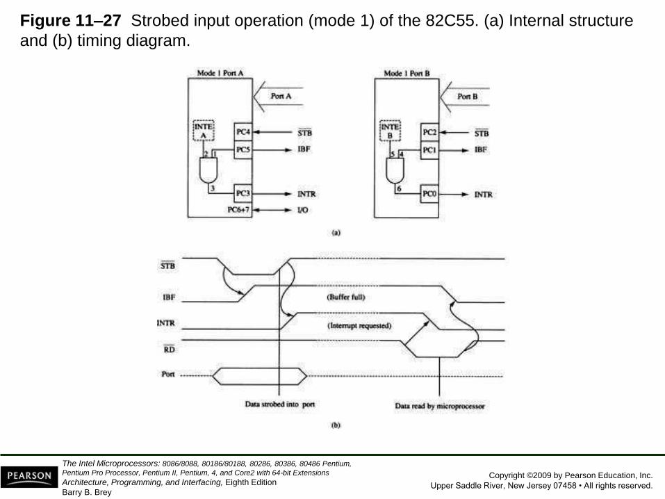
• Fig 11–27 shows how both ports are
structured for mode 1 strobed input operation.
Copyright ©2009 by Pearson Education, Inc.
Upper Saddle River, New Jersey 07458 • All rights reserved.
The Intel Microprocessors: 8086/8088, 80186/80188, 80286, 80386, 80486 Pentium,
Pentium Pro Processor, Pentium II, Pentium, 4, and Core2 with 64-bit Extensions
Architecture, Programming, and Interfacing, Eighth Edition
Barry B. Brey
Figure 11–27 Strobed input operation (mode 1) of the 82C55. (a) Internal structure
and (b) timing diagram.

Copyright ©2009 by Pearson Education, Inc.
Upper Saddle River, New Jersey 07458 • All rights reserved.
The Intel Microprocessors: 8086/8088, 80186/80188, 80286, 80386, 80486 Pentium,
Pentium Pro Processor, Pentium II, Pentium, 4, and Core2 with 64-bit Extensions
Architecture, Programming, and Interfacing, Eighth Edition
Barry B. Brey
Signal Definitions for Mode 1
Strobed Input
STB • The strobe input loads data to the port latch,
which holds the information until it is input to
the microprocessor via the IN instruction.
IBF
• Input buffer full is an output indicating that
the input latch contains information.

Copyright ©2009 by Pearson Education, Inc.
Upper Saddle River, New Jersey 07458 • All rights reserved.
The Intel Microprocessors: 8086/8088, 80186/80188, 80286, 80386, 80486 Pentium,
Pentium Pro Processor, Pentium II, Pentium, 4, and Core2 with 64-bit Extensions
Architecture, Programming, and Interfacing, Eighth Edition
Barry B. Brey
INTR
• Interrupt request is an output that requests
an interrupt. The INTR pin becomes a logic 1
when STB returns to a logic 1. Cleared when
data are input from the port by the processor.
INTE
• Interrupt enable signal is neither input nor
output; it is an internal bit programmed via
port PC4 (port A) or PC2 (port B) bit position.

Copyright ©2009 by Pearson Education, Inc.
Upper Saddle River, New Jersey 07458 • All rights reserved.
The Intel Microprocessors: 8086/8088, 80186/80188, 80286, 80386, 80486 Pentium,
Pentium Pro Processor, Pentium II, Pentium, 4, and Core2 with 64-bit Extensions
Architecture, Programming, and Interfacing, Eighth Edition
Barry B. Brey
PC7, PC6
• The port C pins 7 and 6 are general-purpose
I/O pins that are available for any purpose.
Copyright ©2009 by Pearson Education, Inc.
Upper Saddle River, New Jersey 07458 • All rights reserved.
The Intel Microprocessors: 8086/8088, 80186/80188, 80286, 80386, 80486 Pentium,
Pentium Pro Processor, Pentium II, Pentium, 4, and Core2 with 64-bit Extensions
Architecture, Programming, and Interfacing, Eighth Edition
Barry B. Brey
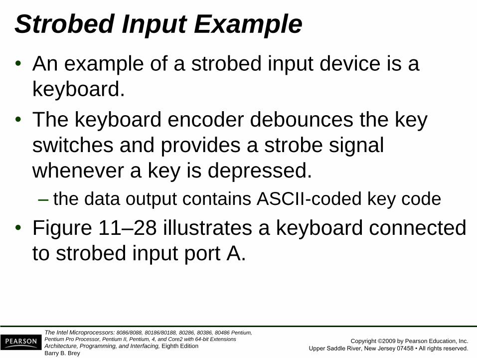
Strobed Input Example
• An example of a strobed input device is a
keyboard.
• The keyboard encoder debounces the key
switches and provides a strobe signal
whenever a key is depressed.
– the data output contains ASCII-coded key code
• Figure 11–28 illustrates a keyboard connected
to strobed input port A.

Copyright ©2009 by Pearson Education, Inc.
Upper Saddle River, New Jersey 07458 • All rights reserved.
The Intel Microprocessors: 8086/8088, 80186/80188, 80286, 80386, 80486 Pentium,
Pentium Pro Processor, Pentium II, Pentium, 4, and Core2 with 64-bit Extensions
Architecture, Programming, and Interfacing, Eighth Edition
Barry B. Brey
Figure 11–28 Using the 82C55 for strobed input operation of a keyboard.

Copyright ©2009 by Pearson Education, Inc.
Upper Saddle River, New Jersey 07458 • All rights reserved.
The Intel Microprocessors: 8086/8088, 80186/80188, 80286, 80386, 80486 Pentium,
Pentium Pro Processor, Pentium II, Pentium, 4, and Core2 with 64-bit Extensions
Architecture, Programming, and Interfacing, Eighth Edition
Barry B. Brey
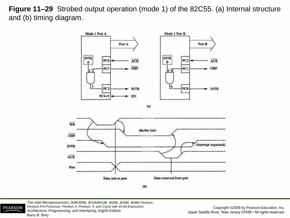
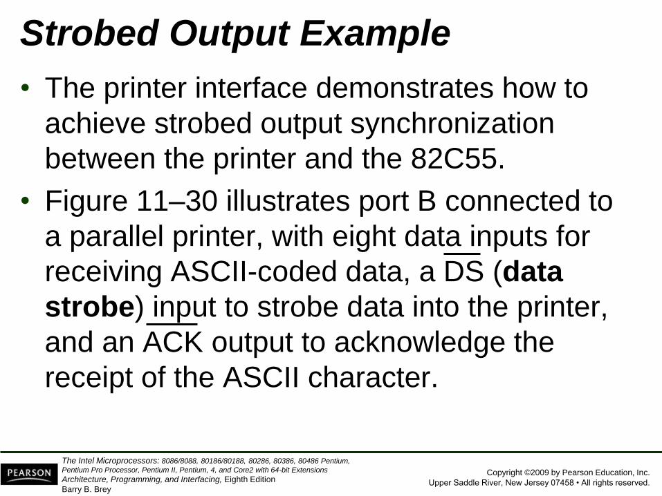
Mode 1 Strobed Output
• Fig 11–29 shows the internal configuration
and timing diagram of 82C55 when operated
as a strobed output device under mode 1.
• Strobed output operation is similar to mode 0
output operation.
– except control signals are included to provide
handshaking
• When data are written to a strobed output port,
the output buffer full signal becomes logic 0
to indicate data are present in the port latch.
Copyright ©2009 by Pearson Education, Inc.
Upper Saddle River, New Jersey 07458 • All rights reserved.
The Intel Microprocessors: 8086/8088, 80186/80188, 80286, 80386, 80486 Pentium,
Pentium Pro Processor, Pentium II, Pentium, 4, and Core2 with 64-bit Extensions
Architecture, Programming, and Interfacing, Eighth Edition
Barry B. Brey
Figure 11–29 Strobed output operation (mode 1) of the 82C55. (a) Internal structure
and (b) timing diagram.

Copyright ©2009 by Pearson Education, Inc.
Upper Saddle River, New Jersey 07458 • All rights reserved.
The Intel Microprocessors: 8086/8088, 80186/80188, 80286, 80386, 80486 Pentium,
Pentium Pro Processor, Pentium II, Pentium, 4, and Core2 with 64-bit Extensions
Architecture, Programming, and Interfacing, Eighth Edition
Barry B. Brey
Signal Definitions for Mode 1
Strobed Output
OBF • Output buffer full goes low whenever data
are output (OUT) to the port A or B latch. The
signal is set to logic 1 when the ACK pulse
returns from the external device.

Copyright ©2009 by Pearson Education, Inc.
Upper Saddle River, New Jersey 07458 • All rights reserved.
The Intel Microprocessors: 8086/8088, 80186/80188, 80286, 80386, 80486 Pentium,
Pentium Pro Processor, Pentium II, Pentium, 4, and Core2 with 64-bit Extensions
Architecture, Programming, and Interfacing, Eighth Edition
Barry B. Brey
ACK
• The acknowledge signal causes the OBF
pin to return to logic 1. The ACK signal is a
response from an external device, indicating
that it has received data from the 82C55 port.
INTR
• Interrupt request often interrupts the
processor when the external device receives
the data via the ACK signal. Qualified by the
internal INTE (interrupt enable) bit.

Copyright ©2009 by Pearson Education, Inc.
Upper Saddle River, New Jersey 07458 • All rights reserved.
The Intel Microprocessors: 8086/8088, 80186/80188, 80286, 80386, 80486 Pentium,
Pentium Pro Processor, Pentium II, Pentium, 4, and Core2 with 64-bit Extensions
Architecture, Programming, and Interfacing, Eighth Edition
Barry B. Brey
INTE
• Interrupt enable is neither input nor output;
it is an internal bit programmed to enable or
disable the INTR pin. INTE A is programmed
using PC6 bit. INTE B is programmed using
the PC2 bit.
PC4, PC5
• Port C pins PC4 and PC5 are general-purpose
I/O pins. The bit set and reset command is
used to set or reset these two pins.
Copyright ©2009 by Pearson Education, Inc.
Upper Saddle River, New Jersey 07458 • All rights reserved.
The Intel Microprocessors: 8086/8088, 80186/80188, 80286, 80386, 80486 Pentium,
Pentium Pro Processor, Pentium II, Pentium, 4, and Core2 with 64-bit Extensions
Architecture, Programming, and Interfacing, Eighth Edition
Barry B. Brey
Strobed Output Example
• The printer interface demonstrates how to
achieve strobed output synchronization
between the printer and the 82C55.
• Figure 11–30 illustrates port B connected to
a parallel printer, with eight data inputs for
receiving ASCII-coded data, a DS (data
strobe) input to strobe data into the printer,
and an ACK output to acknowledge the
receipt of the ASCII character.

Copyright ©2009 by Pearson Education, Inc.
Upper Saddle River, New Jersey 07458 • All rights reserved.
The Intel Microprocessors: 8086/8088, 80186/80188, 80286, 80386, 80486 Pentium,
Pentium Pro Processor, Pentium II, Pentium, 4, and Core2 with 64-bit Extensions
Architecture, Programming, and Interfacing, Eighth Edition
Barry B. Brey
Figure 11–30 The 82C55 connected to a parallel printer interface that illustrates the
strobed output mode of operation for the 82C55.
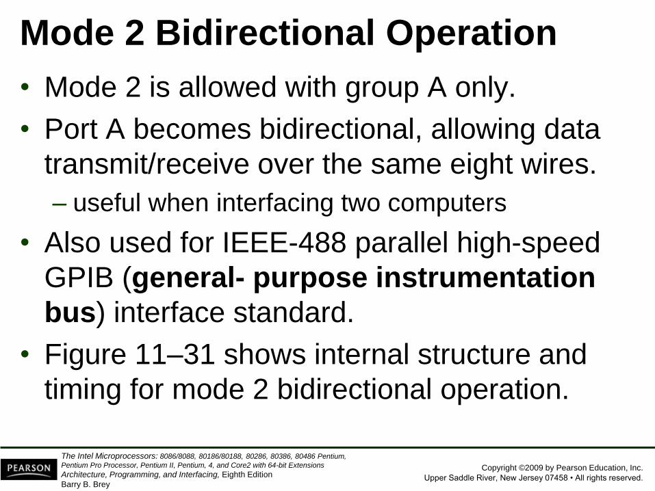
Copyright ©2009 by Pearson Education, Inc.
Upper Saddle River, New Jersey 07458 • All rights reserved.
The Intel Microprocessors: 8086/8088, 80186/80188, 80286, 80386, 80486 Pentium,
Pentium Pro Processor, Pentium II, Pentium, 4, and Core2 with 64-bit Extensions
Architecture, Programming, and Interfacing, Eighth Edition
Barry B. Brey
Mode 2 Bidirectional Operation
• Mode 2 is allowed with group A only.
• Port A becomes bidirectional, allowing data
transmit/receive over the same eight wires.
– useful when interfacing two computers
• Also used for IEEE-488 parallel high-speed
GPIB (general- purpose instrumentation
bus) interface standard.
• Figure 11–31 shows internal structure and
timing for mode 2 bidirectional operation.

Copyright ©2009 by Pearson Education, Inc.
Upper Saddle River, New Jersey 07458 • All rights reserved.
The Intel Microprocessors: 8086/8088, 80186/80188, 80286, 80386, 80486 Pentium,
Pentium Pro Processor, Pentium II, Pentium, 4, and Core2 with 64-bit Extensions
Architecture, Programming, and Interfacing, Eighth Edition
Barry B. Brey
Figure 11–31 Mode 2 operation of the 82C55. (a) Internal structure and (b) timing
diagram.

Copyright ©2009 by Pearson Education, Inc.
Upper Saddle River, New Jersey 07458 • All rights reserved.
The Intel Microprocessors: 8086/8088, 80186/80188, 80286, 80386, 80486 Pentium,
Pentium Pro Processor, Pentium II, Pentium, 4, and Core2 with 64-bit Extensions
Architecture, Programming, and Interfacing, Eighth Edition
Barry B. Brey
• Interrupt request is an output used to
interrupt the microprocessor for input
and output conditions.
Signal Definitions for Bidirectional
Mode 2
OBF • Output buffer full is an output indicating
the output buffer contains data for the
bidirectional bus.
INTR

Copyright ©2009 by Pearson Education, Inc.
Upper Saddle River, New Jersey 07458 • All rights reserved.
The Intel Microprocessors: 8086/8088, 80186/80188, 80286, 80386, 80486 Pentium,
Pentium Pro Processor, Pentium II, Pentium, 4, and Core2 with 64-bit Extensions
Architecture, Programming, and Interfacing, Eighth Edition
Barry B. Brey
ACK
• Acknowledge is an input that enables the
three-state buffers so that data can appear
on port A. If ACK is logic 1, the output buffers
of port A are at their high-impedance state.
STB
• The strobe input loads the port A input latch
with external data from the bidirectional
port A bus.

Copyright ©2009 by Pearson Education, Inc.
Upper Saddle River, New Jersey 07458 • All rights reserved.
The Intel Microprocessors: 8086/8088, 80186/80188, 80286, 80386, 80486 Pentium,
Pentium Pro Processor, Pentium II, Pentium, 4, and Core2 with 64-bit Extensions
Architecture, Programming, and Interfacing, Eighth Edition
Barry B. Brey
PC0, PC1, and PC2
• These pins are general-purpose I/O pins in
mode 2 controlled by the bit set and reset
command.
Copyright ©2009 by Pearson Education, Inc.
Upper Saddle River, New Jersey 07458 • All rights reserved.
The Intel Microprocessors: 8086/8088, 80186/80188, 80286, 80386, 80486 Pentium,
Pentium Pro Processor, Pentium II, Pentium, 4, and Core2 with 64-bit Extensions
Architecture, Programming, and Interfacing, Eighth Edition
Barry B. Brey
IBF
• Input buffer full is an output used to signal
that the input buffer contains data for the
external bidirectional bus.
INTE
• Interrupt enable are internal bits (INTE1 &
INTE2) that enable the INTR pin. The state
of the INTR pin is controlled through port C
bits PC6 (INTE1) and PC4 (INTE2).

Copyright ©2009 by Pearson Education, Inc.
Upper Saddle River, New Jersey 07458 • All rights reserved.
The Intel Microprocessors: 8086/8088, 80186/80188, 80286, 80386, 80486 Pentium,
Pentium Pro Processor, Pentium II, Pentium, 4, and Core2 with 64-bit Extensions
Architecture, Programming, and Interfacing, Eighth Edition
Barry B. Brey
The Bidirectional Bus
• The bidirectional bus is used by referencing
port A with the IN and OUT instructions.
• To transmit data through the bidirectional bus,
the program first tests to determine whether
the output buffer is empty.
– if so, data are sent to the output buffer via OUT
• The external circuitry also monitors the signal
to decide whether the microprocessor has
sent data to the bus.
Copyright ©2009 by Pearson Education, Inc.
Upper Saddle River, New Jersey 07458 • All rights reserved.
The Intel Microprocessors: 8086/8088, 80186/80188, 80286, 80386, 80486 Pentium,
Pentium Pro Processor, Pentium II, Pentium, 4, and Core2 with 64-bit Extensions
Architecture, Programming, and Interfacing, Eighth Edition
Barry B. Brey
• To receive data through the bidirectional port
A bus, IBF is tested with software to decide
whether data have been strobed into the port.
– if IBF = 1, data is input using IN
• The external interface sends data to the port
by using the STB signal.
– the IBF signal becomes logic 1 and data at
port A are held inside the port in a latch
• When the IN executes, the IBF bit is cleared
and data in the port are moved into AL.
• See Example 11–21 for a procedure.
Copyright ©2009 by Pearson Education, Inc.
Upper Saddle River, New Jersey 07458 • All rights reserved.
The Intel Microprocessors: 8086/8088, 80186/80188, 80286, 80386, 80486 Pentium,
Pentium Pro Processor, Pentium II, Pentium, 4, and Core2 with 64-bit Extensions
Architecture, Programming, and Interfacing, Eighth Edition
Barry B. Brey
• The INTR (interrupt request) pin can be
activated from both directions of data flow
through the bus.
• If INTR is enabled by both INTE bits, the
output and input buffers both cause interrupt
requests.
• This occurs when data are strobed into the
buffer using STB or when data are written
using OUT.
Copyright ©2009 by Pearson Education, Inc.
Upper Saddle River, New Jersey 07458 • All rights reserved.
The Intel Microprocessors: 8086/8088, 80186/80188, 80286, 80386, 80486 Pentium,
Pentium Pro Processor, Pentium II, Pentium, 4, and Core2 with 64-bit Extensions
Architecture, Programming, and Interfacing, Eighth Edition
Barry B. Brey
82C55 Mode Summary
• Figure 11–32 shows a graphical summary of
the three modes of operation for the 82C55.
• Mode 0 provides simple I/O.
• Mode 1 provides strobed I/O.
• Mode 2 provides bidirectional I/O.
• These modes are selected through the
command register of the 82C55.

Copyright ©2009 by Pearson Education, Inc.
Upper Saddle River, New Jersey 07458 • All rights reserved.
The Intel Microprocessors: 8086/8088, 80186/80188, 80286, 80386, 80486 Pentium,
Pentium Pro Processor, Pentium II, Pentium, 4, and Core2 with 64-bit Extensions
Architecture, Programming, and Interfacing, Eighth Edition
Barry B. Brey
Figure 11–32 A summary of the port connections for the 82C55 PIA.

Copyright ©2009 by Pearson Education, Inc.
Upper Saddle River, New Jersey 07458 • All rights reserved.
The Intel Microprocessors: 8086/8088, 80186/80188, 80286, 80386, 80486 Pentium,
Pentium Pro Processor, Pentium II, Pentium, 4, and Core2 with 64-bit Extensions
Architecture, Programming, and Interfacing, Eighth Edition
Barry B. Brey
The Serial EEPROM Interface
• In Chapter 10, Figure 10–23, a serial
EEPROM is illustrated, but at that point in
the text, no I/O existed for an interface.
• Suppose that port C of an 82C55 is used for
connection to this interface and software is
needed to drive the interface.
• The PC0 pin is programmed as an output to
send data and as an input to receive data
from the EEPROM.

Copyright ©2009 by Pearson Education, Inc.
Upper Saddle River, New Jersey 07458 • All rights reserved.
The Intel Microprocessors: 8086/8088, 80186/80188, 80286, 80386, 80486 Pentium,
Pentium Pro Processor, Pentium II, Pentium, 4, and Core2 with 64-bit Extensions
Architecture, Programming, and Interfacing, Eighth Edition
Barry B. Brey
Chapter 10, Figure 10–23 A serial EEPROM interface.
– this memory interface
has two signal lines
– one is a serial clock
(SCL); the other a
bidirectional serial data
line (SDA)
– not meant to replace
system main memory
– it is fast enough for music
or other low-speed data

Copyright ©2009 by Pearson Education, Inc.
Upper Saddle River, New Jersey 07458 • All rights reserved.
The Intel Microprocessors: 8086/8088, 80186/80188, 80286, 80386, 80486 Pentium,
Pentium Pro Processor, Pentium II, Pentium, 4, and Core2 with 64-bit Extensions
Architecture, Programming, and Interfacing, Eighth Edition
Barry B. Brey
• Refer to Figure 10–24.
• The data format for the software for reading
and writing data to the EEPROM is also
illustrated in Example 11–22.
• This software is written in C with some
assembly language, but it can also be
developed in assembly language.
• I/O port address for the command register is
0x1203, and 0x1202 for the port C register.
– the time delay should be 1.25 µs for a data
rate of 400 KHz

Copyright ©2009 by Pearson Education, Inc.
Upper Saddle River, New Jersey 07458 • All rights reserved.
The Intel Microprocessors: 8086/8088, 80186/80188, 80286, 80386, 80486 Pentium,
Pentium Pro Processor, Pentium II, Pentium, 4, and Core2 with 64-bit Extensions
Architecture, Programming, and Interfacing, Eighth Edition
Barry B. Brey
Chapter 10, Figure 10–24 Data signals to the serial EEPROM for a read or a write.
– the serial data contains
the address in the first
byte as well as a device
code of 1010, which
represents the EEPROM
– other serial devices have
different device codes
– this is followed by the
memory location and the
data in additional bytes

Copyright ©2009 by Pearson Education, Inc.
Upper Saddle River, New Jersey 07458 • All rights reserved.
The Intel Microprocessors: 8086/8088, 80186/80188, 80286, 80386, 80486 Pentium,
Pentium Pro Processor, Pentium II, Pentium, 4, and Core2 with 64-bit Extensions
Architecture, Programming, and Interfacing, Eighth Edition
Barry B. Brey
11–4 8254 PROGRAMMABLE
INTERVAL TIMER
• The 8254 consists of three independent
16-bit programmable counters (timers).
• Each counter is capable of counting in binary
or binary-coded decimal (BCD).
– maximum allowable input frequency to any
counter is 10 MHz
• Useful where the microprocessor must
control real-time events.

Copyright ©2009 by Pearson Education, Inc.
Upper Saddle River, New Jersey 07458 • All rights reserved.
The Intel Microprocessors: 8086/8088, 80186/80188, 80286, 80386, 80486 Pentium,
Pentium Pro Processor, Pentium II, Pentium, 4, and Core2 with 64-bit Extensions
Architecture, Programming, and Interfacing, Eighth Edition
Barry B. Brey
• Usage includes real-time clocks, event
counters, and motor speed/direction control.
• Timer appears in the PC decoded at ports
40H–43H to do the following:
– 1. Generate a basic timer interrupt that occurs
at approximately 18.2 Hz
– 2. Cause the DRAM memory system to be
refreshed
– 3. Provide a timing source to the internal
speaker and other devices.
• Timer in the PC is an 8253 instead of 8254.

Copyright ©2009 by Pearson Education, Inc.
Upper Saddle River, New Jersey 07458 • All rights reserved.
The Intel Microprocessors: 8086/8088, 80186/80188, 80286, 80386, 80486 Pentium,
Pentium Pro Processor, Pentium II, Pentium, 4, and Core2 with 64-bit Extensions
Architecture, Programming, and Interfacing, Eighth Edition
Barry B. Brey
8254 Functional Description
• Figure 11–33 shows the pin-out of the 8254,
a higher-speed version of the 8253, and a
diagram of one of the three counters.
• Each timer contains:
– a CLK input which provides the basic operating
frequency to the timer
– a gate input pin which controls the timer in some
modes
– an output (OUT) connection to obtain the output
of the timer

Copyright ©2009 by Pearson Education, Inc.
Upper Saddle River, New Jersey 07458 • All rights reserved.
The Intel Microprocessors: 8086/8088, 80186/80188, 80286, 80386, 80486 Pentium,
Pentium Pro Processor, Pentium II, Pentium, 4, and Core2 with 64-bit Extensions
Architecture, Programming, and Interfacing, Eighth Edition
Barry B. Brey
Figure 11–33 The 8254 programmable interval timer. (a) Internal structure and (b)
pin-out. (Courtesy of Intel Corporation.)

Copyright ©2009 by Pearson Education, Inc.
Upper Saddle River, New Jersey 07458 • All rights reserved.
The Intel Microprocessors: 8086/8088, 80186/80188, 80286, 80386, 80486 Pentium,
Pentium Pro Processor, Pentium II, Pentium, 4, and Core2 with 64-bit Extensions
Architecture, Programming, and Interfacing, Eighth Edition
Barry B. Brey
• The signals that connect to the processor are
the data bus pins (D7–D0), RD, WR, CS, and
address inputs A1 and A0.
• Address inputs are present to select any of
the four internal registers.
– used for programming, reading, or writing to a
counter
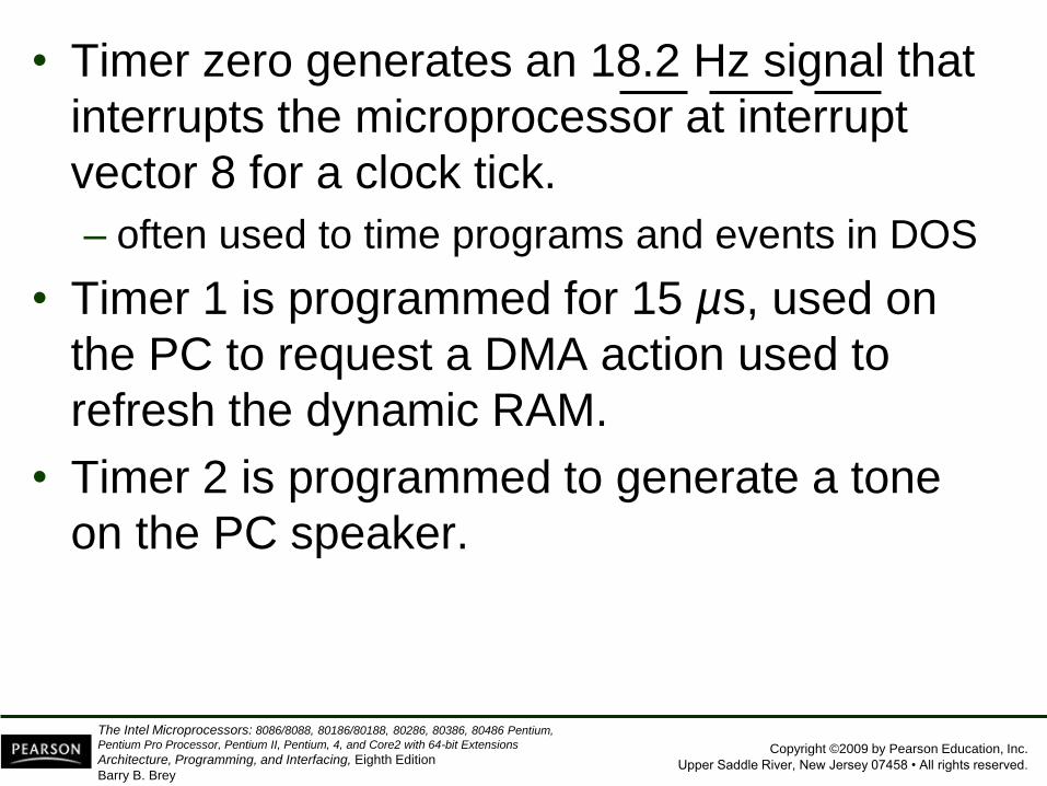
Copyright ©2009 by Pearson Education, Inc.
Upper Saddle River, New Jersey 07458 • All rights reserved.
The Intel Microprocessors: 8086/8088, 80186/80188, 80286, 80386, 80486 Pentium,
Pentium Pro Processor, Pentium II, Pentium, 4, and Core2 with 64-bit Extensions
Architecture, Programming, and Interfacing, Eighth Edition
Barry B. Brey
• Timer zero generates an 18.2 Hz signal that
interrupts the microprocessor at interrupt
vector 8 for a clock tick.
– often used to time programs and events in DOS
• Timer 1 is programmed for 15 µs, used on
the PC to request a DMA action used to
refresh the dynamic RAM.
• Timer 2 is programmed to generate a tone
on the PC speaker.

Copyright ©2009 by Pearson Education, Inc.
Upper Saddle River, New Jersey 07458 • All rights reserved.
The Intel Microprocessors: 8086/8088, 80186/80188, 80286, 80386, 80486 Pentium,
Pentium Pro Processor, Pentium II, Pentium, 4, and Core2 with 64-bit Extensions
Architecture, Programming, and Interfacing, Eighth Edition
Barry B. Brey
• The address inputs select one of four internal
registers within the 8254. See Table 11–4 for
the function of the A1 and A0 address bits.
Pin Definitions for 8254
CLK • The clock input is the timing source for each
of the internal counters. This input is often
connected to the PCLK signal from the
microprocessor system bus controller.
A0, A1
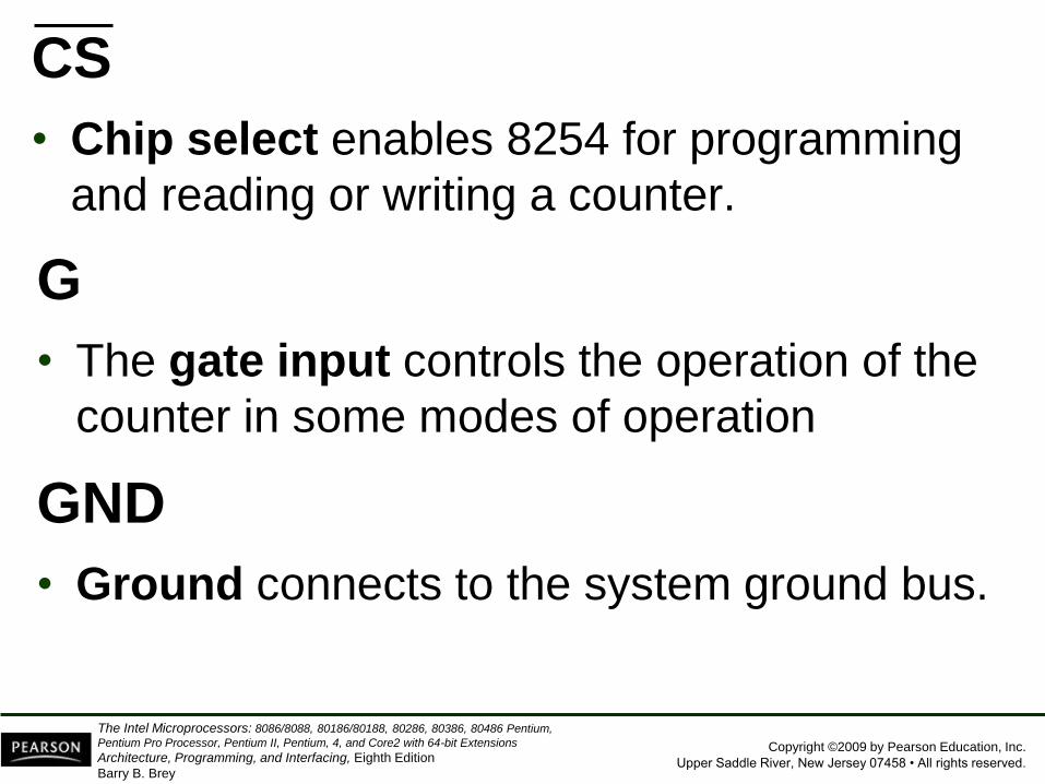
Copyright ©2009 by Pearson Education, Inc.
Upper Saddle River, New Jersey 07458 • All rights reserved.
The Intel Microprocessors: 8086/8088, 80186/80188, 80286, 80386, 80486 Pentium,
Pentium Pro Processor, Pentium II, Pentium, 4, and Core2 with 64-bit Extensions
Architecture, Programming, and Interfacing, Eighth Edition
Barry B. Brey
CS
• Chip select enables 8254 for programming
and reading or writing a counter.
G
• The gate input controls the operation of the
counter in some modes of operation
GND
• Ground connects to the system ground bus.

Copyright ©2009 by Pearson Education, Inc.
Upper Saddle River, New Jersey 07458 • All rights reserved.
The Intel Microprocessors: 8086/8088, 80186/80188, 80286, 80386, 80486 Pentium,
Pentium Pro Processor, Pentium II, Pentium, 4, and Core2 with 64-bit Extensions
Architecture, Programming, and Interfacing, Eighth Edition
Barry B. Brey
OUT
• A counter output is where the waveform
generated by the timer is available.
RD
• Read causes data to be read from the 8254
and often connects to the IORC signal.
Vcc
• Power connects to the +5.0 V power supply.

Copyright ©2009 by Pearson Education, Inc.
Upper Saddle River, New Jersey 07458 • All rights reserved.
The Intel Microprocessors: 8086/8088, 80186/80188, 80286, 80386, 80486 Pentium,
Pentium Pro Processor, Pentium II, Pentium, 4, and Core2 with 64-bit Extensions
Architecture, Programming, and Interfacing, Eighth Edition
Barry B. Brey
WR
• Write causes data to be written to the 8254
and often connects to write strobe IOWC.
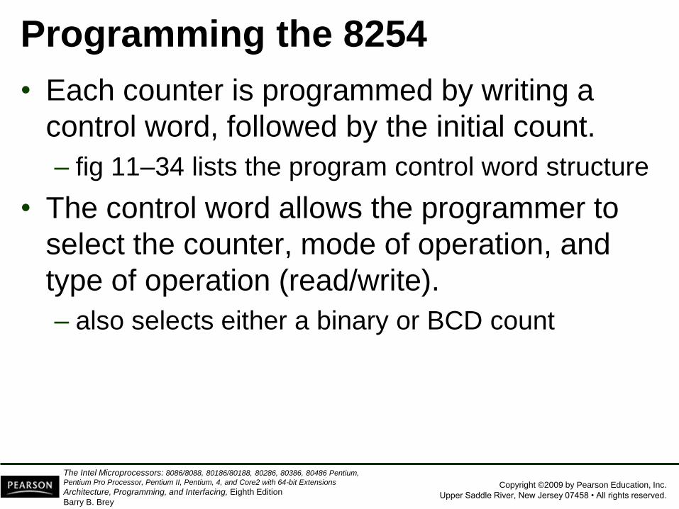
Copyright ©2009 by Pearson Education, Inc.
Upper Saddle River, New Jersey 07458 • All rights reserved.
The Intel Microprocessors: 8086/8088, 80186/80188, 80286, 80386, 80486 Pentium,
Pentium Pro Processor, Pentium II, Pentium, 4, and Core2 with 64-bit Extensions
Architecture, Programming, and Interfacing, Eighth Edition
Barry B. Brey
Programming the 8254
• Each counter is programmed by writing a
control word, followed by the initial count.
– fig 11–34 lists the program control word structure
• The control word allows the programmer to
select the counter, mode of operation, and
type of operation (read/write).
– also selects either a binary or BCD count

Copyright ©2009 by Pearson Education, Inc.
Upper Saddle River, New Jersey 07458 • All rights reserved.
The Intel Microprocessors: 8086/8088, 80186/80188, 80286, 80386, 80486 Pentium,
Pentium Pro Processor, Pentium II, Pentium, 4, and Core2 with 64-bit Extensions
Architecture, Programming, and Interfacing, Eighth Edition
Barry B. Brey
Figure 11–34 The control word for the 8254-2 timer.

Copyright ©2009 by Pearson Education, Inc.
Upper Saddle River, New Jersey 07458 • All rights reserved.
The Intel Microprocessors: 8086/8088, 80186/80188, 80286, 80386, 80486 Pentium,
Pentium Pro Processor, Pentium II, Pentium, 4, and Core2 with 64-bit Extensions
Architecture, Programming, and Interfacing, Eighth Edition
Barry B. Brey
• Each counter may be programmed with a
count of 1 to FFFFH; A count of 0 is equal
to FFFFH+l (65,536) or 10,000 in BCD.
• Timer 0 is used in the PC with a divide-by
count of 64K (FFFFH) to generate the
18.2 Hz (18.196 Hz) interrupt clock tick.
– timer 0 has a clock input frequency of
4.77 MHz + 4 or 1.1925 MHz
• The order of programming is important for
each counter, but programming of different
counters may be interleaved for better control.
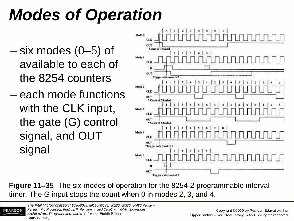
Copyright ©2009 by Pearson Education, Inc.
Upper Saddle River, New Jersey 07458 • All rights reserved.
The Intel Microprocessors: 8086/8088, 80186/80188, 80286, 80386, 80486 Pentium,
Pentium Pro Processor, Pentium II, Pentium, 4, and Core2 with 64-bit Extensions
Architecture, Programming, and Interfacing, Eighth Edition
Barry B. Brey
Figure 11–35 The six modes of operation for the 8254-2 programmable interval
timer. The G input stops the count when 0 in modes 2, 3, and 4.
Modes of Operation
– six modes (0–5) of
available to each of
the 8254 counters
– each mode functions
with the CLK input,
the gate (G) control
signal, and OUT
signal

Copyright ©2009 by Pearson Education, Inc.
Upper Saddle River, New Jersey 07458 • All rights reserved.
The Intel Microprocessors: 8086/8088, 80186/80188, 80286, 80386, 80486 Pentium,
Pentium Pro Processor, Pentium II, Pentium, 4, and Core2 with 64-bit Extensions
Architecture, Programming, and Interfacing, Eighth Edition
Barry B. Brey
Mode 0
• Allows 8254 to be used as an events counter.
• Output becomes logic 0 when the control
word is written and remains until N plus the
number of programmed counts.
• Note that gate (G) input must be logic 1 to
allow the counter to count.
• If G becomes logic 0 in the middle of the
count, the counter will stop until G again
becomes logic 1.

Copyright ©2009 by Pearson Education, Inc.
Upper Saddle River, New Jersey 07458 • All rights reserved.
The Intel Microprocessors: 8086/8088, 80186/80188, 80286, 80386, 80486 Pentium,
Pentium Pro Processor, Pentium II, Pentium, 4, and Core2 with 64-bit Extensions
Architecture, Programming, and Interfacing, Eighth Edition
Barry B. Brey
Mode 1
• Causes function as a retriggerable,
monostable multivibrator (one-shot).
• G input triggers the counter so it develops a
pulse at the OUT connection that becomes
logic 0 for the duration of the count.
– if the count is 10, the OUT connection goes
low for 10 clocking periods when triggered
• If G input occurs within the output pulse, the
counter is reloaded and the OUT connection
continues for the total length of the count.

Copyright ©2009 by Pearson Education, Inc.
Upper Saddle River, New Jersey 07458 • All rights reserved.
The Intel Microprocessors: 8086/8088, 80186/80188, 80286, 80386, 80486 Pentium,
Pentium Pro Processor, Pentium II, Pentium, 4, and Core2 with 64-bit Extensions
Architecture, Programming, and Interfacing, Eighth Edition
Barry B. Brey
Mode 2
• Allows the counter to generate a series of
continuous pulses one clock pulse wide.
– pulse separation is determined by the count
• For a count of 10, output is logic 1 for nine
clock periods and low for one clock period.
• The cycle is repeated until the counter is
programmed with a new count or until the G
pin is placed at logic 0.
– G input must be logic 1 for this mode to
generate a continuous series of pulses
Copyright ©2009 by Pearson Education, Inc.
Upper Saddle River, New Jersey 07458 • All rights reserved.
The Intel Microprocessors: 8086/8088, 80186/80188, 80286, 80386, 80486 Pentium,
Pentium Pro Processor, Pentium II, Pentium, 4, and Core2 with 64-bit Extensions
Architecture, Programming, and Interfacing, Eighth Edition
Barry B. Brey
Mode 3
• Generates a continuous square wave at the
OUT connection, provided the G pin is logic 1.
• If the count is even, output is high for one half
of the count and low for one half of the count.
• If the count is odd, output is high for one
clocking period longer than it is low.
– if the counter is programmed for a count of 5,
the output is high for three clocks and low for
two clocks

Copyright ©2009 by Pearson Education, Inc.
Upper Saddle River, New Jersey 07458 • All rights reserved.
The Intel Microprocessors: 8086/8088, 80186/80188, 80286, 80386, 80486 Pentium,
Pentium Pro Processor, Pentium II, Pentium, 4, and Core2 with 64-bit Extensions
Architecture, Programming, and Interfacing, Eighth Edition
Barry B. Brey
Mode 4
• Allows a single pulse at the output.
• If count is programmed as 10, output is high
for 10 clocking periods and low for one period.
– the cycle does not begin until the counter
is loaded with its complete count
• Operates as a software triggered one-shot.
• As with modes 2 and 3, this mode also uses
the G input to enable the counter.
– G input must be logic 1 for the counter to
operate for these three modes

Copyright ©2009 by Pearson Education, Inc.
Upper Saddle River, New Jersey 07458 • All rights reserved.
The Intel Microprocessors: 8086/8088, 80186/80188, 80286, 80386, 80486 Pentium,
Pentium Pro Processor, Pentium II, Pentium, 4, and Core2 with 64-bit Extensions
Architecture, Programming, and Interfacing, Eighth Edition
Barry B. Brey
Mode 5
• A hardware triggered one-shot that functions
as mode 4.
– except it is started by a trigger pulse on the
G pin instead of by software
• This mode is also similar to mode 1 because
it is retriggerable.

Copyright ©2009 by Pearson Education, Inc.
Upper Saddle River, New Jersey 07458 • All rights reserved.
The Intel Microprocessors: 8086/8088, 80186/80188, 80286, 80386, 80486 Pentium,
Pentium Pro Processor, Pentium II, Pentium, 4, and Core2 with 64-bit Extensions
Architecture, Programming, and Interfacing, Eighth Edition
Barry B. Brey
Generating a Waveform with the
8254
• Fig 11–36 shows an 8254 connected to I/O
ports 0700H, 0702H, 0704H, and 0706H of an
80386SX.
• The addresses are decoded by using a PLD
that also generates a write strobe signal for
the 8254, which is connected to the low-order
data bus connections.

Copyright ©2009 by Pearson Education, Inc.
Upper Saddle River, New Jersey 07458 • All rights reserved.
The Intel Microprocessors: 8086/8088, 80186/80188, 80286, 80386, 80486 Pentium,
Pentium Pro Processor, Pentium II, Pentium, 4, and Core2 with 64-bit Extensions
Architecture, Programming, and Interfacing, Eighth Edition
Barry B. Brey
Figure 11–36 The 8254 interfaced to an 8 MHz 8086 so that it generates a 100 KHz
square wave at OUT0 and a 200 KHz continuous pulse at OUT1.

Copyright ©2009 by Pearson Education, Inc.
Upper Saddle River, New Jersey 07458 • All rights reserved.
The Intel Microprocessors: 8086/8088, 80186/80188, 80286, 80386, 80486 Pentium,
Pentium Pro Processor, Pentium II, Pentium, 4, and Core2 with 64-bit Extensions
Architecture, Programming, and Interfacing, Eighth Edition
Barry B. Brey
• The PLD also generates a wait signal for the
microprocessor that causes two wait states
when the 8254 is accessed.
• The wait state generator connected to the
microprocessor actually controls the number
of wait states inserted into the timing.
• Example 11–24 lists the program that
generates a 100 KHz square-wave at OUT0
and a 200 KHz continuous pulse at OUT1.

Copyright ©2009 by Pearson Education, Inc.
Upper Saddle River, New Jersey 07458 • All rights reserved.
The Intel Microprocessors: 8086/8088, 80186/80188, 80286, 80386, 80486 Pentium,
Pentium Pro Processor, Pentium II, Pentium, 4, and Core2 with 64-bit Extensions
Architecture, Programming, and Interfacing, Eighth Edition
Barry B. Brey
Reading a Counter
• Each counter has an internal latch read with
the read counter port operation.
– the latches will normally follow the count
• If counter contents are needed, the latch can
remember the count by programming the
counter latch control word.
• See Figure 11–37.
– counter contents are held in a latch until read

Copyright ©2009 by Pearson Education, Inc.
Upper Saddle River, New Jersey 07458 • All rights reserved.
The Intel Microprocessors: 8086/8088, 80186/80188, 80286, 80386, 80486 Pentium,
Pentium Pro Processor, Pentium II, Pentium, 4, and Core2 with 64-bit Extensions
Architecture, Programming, and Interfacing, Eighth Edition
Barry B. Brey
Figure 11–37 The 8254-2 counter latch control word.
Copyright ©2009 by Pearson Education, Inc.
Upper Saddle River, New Jersey 07458 • All rights reserved.
The Intel Microprocessors: 8086/8088, 80186/80188, 80286, 80386, 80486 Pentium,
Pentium Pro Processor, Pentium II, Pentium, 4, and Core2 with 64-bit Extensions
Architecture, Programming, and Interfacing, Eighth Edition
Barry B. Brey
• When a read from the latch or counter is
programmed, the latch tracks the contents.
• When necessary for contents of more than
one counter to be read at the same time, the
read-back control word is used
• Illustrated in Figure 11–38.

Copyright ©2009 by Pearson Education, Inc.
Upper Saddle River, New Jersey 07458 • All rights reserved.
The Intel Microprocessors: 8086/8088, 80186/80188, 80286, 80386, 80486 Pentium,
Pentium Pro Processor, Pentium II, Pentium, 4, and Core2 with 64-bit Extensions
Architecture, Programming, and Interfacing, Eighth Edition
Barry B. Brey
Figure 11–38 The 8254-2 read-back control word.

Copyright ©2009 by Pearson Education, Inc.
Upper Saddle River, New Jersey 07458 • All rights reserved.
The Intel Microprocessors: 8086/8088, 80186/80188, 80286, 80386, 80486 Pentium,
Pentium Pro Processor, Pentium II, Pentium, 4, and Core2 with 64-bit Extensions
Architecture, Programming, and Interfacing, Eighth Edition
Barry B. Brey
• With the read-back control word, the CNT bit
is logic 0 to cause the counters selected by
CNT0, CNT1, and CNT2 to be latched.
• If the status register is to be latched, then the
bit is placed at logic 0.
• Figure 11–39 shows the status register,
which shows:
– the state of the output pin
– whether the counter is at its null state (0)
– how the counter is programmed

Copyright ©2009 by Pearson Education, Inc.
Upper Saddle River, New Jersey 07458 • All rights reserved.
The Intel Microprocessors: 8086/8088, 80186/80188, 80286, 80386, 80486 Pentium,
Pentium Pro Processor, Pentium II, Pentium, 4, and Core2 with 64-bit Extensions
Architecture, Programming, and Interfacing, Eighth Edition
Barry B. Brey
Figure 11–39 The 8254-2 status register.
Copyright ©2009 by Pearson Education, Inc.
Upper Saddle River, New Jersey 07458 • All rights reserved.
The Intel Microprocessors: 8086/8088, 80186/80188, 80286, 80386, 80486 Pentium,
Pentium Pro Processor, Pentium II, Pentium, 4, and Core2 with 64-bit Extensions
Architecture, Programming, and Interfacing, Eighth Edition
Barry B. Brey
DC Motor Speed and Direction
Control
• An application of 8254 is as a motor speed
controller for a DC motor.
• Fig 11–40 shows the schematic diagram
of the motor and associated driver circuitry.
• It also illustrates the interconnection of the
8254, a flip-flop, and the motor and its driver.

Copyright ©2009 by Pearson Education, Inc.
Upper Saddle River, New Jersey 07458 • All rights reserved.
The Intel Microprocessors: 8086/8088, 80186/80188, 80286, 80386, 80486 Pentium,
Pentium Pro Processor, Pentium II, Pentium, 4, and Core2 with 64-bit Extensions
Architecture, Programming, and Interfacing, Eighth Edition
Barry B. Brey
Figure 11–40 Motor speed and direction control using the 8254 timer.
– if Q output of the 74ALS112 is logic 1,
the motor spins in its forward direction
– if logic 0, the motor spins in reverse
– if flip-flop output alternates between
logic 1 and 0, the motor spins in either
direction at various speeds
– if the duty cycle of the Q output is
50%, the motor will not spin at all and
exhibits some holding torque

Copyright ©2009 by Pearson Education, Inc.
Upper Saddle River, New Jersey 07458 • All rights reserved.
The Intel Microprocessors: 8086/8088, 80186/80188, 80286, 80386, 80486 Pentium,
Pentium Pro Processor, Pentium II, Pentium, 4, and Core2 with 64-bit Extensions
Architecture, Programming, and Interfacing, Eighth Edition
Barry B. Brey
• Fig 11–41 shows some timing diagrams and
effects on the speed/direction of the motor.
• Each counter generates pulses at different
positions to vary the duty cycle at the Q
output of the flip-flop.
• This output is also called pulse width
modulation.
• Example 11–25 lists a procedure that controls
the speed and direction of the motor.

Copyright ©2009 by Pearson Education, Inc.
Upper Saddle River, New Jersey 07458 • All rights reserved.
The Intel Microprocessors: 8086/8088, 80186/80188, 80286, 80386, 80486 Pentium,
Pentium Pro Processor, Pentium II, Pentium, 4, and Core2 with 64-bit Extensions
Architecture, Programming, and Interfacing, Eighth Edition
Barry B. Brey
Figure 11–41 Timing for the motor speed and direction control circuit of Figure 11–
40. (a) No rotation, (b) high-speed rotation in the reverse direction, and (c) high-speed
rotation in the forward direction.
Copyright ©2009 by Pearson Education, Inc.
Upper Saddle River, New Jersey 07458 • All rights reserved.
The Intel Microprocessors: 8086/8088, 80186/80188, 80286, 80386, 80486 Pentium,
Pentium Pro Processor, Pentium II, Pentium, 4, and Core2 with 64-bit Extensions
Architecture, Programming, and Interfacing, Eighth Edition
Barry B. Brey
11–5 16550 PROGRAMMABLE
COMMUNICATIONS INTERFACE
• National Semiconductor Corp’s PC16550D
is a programmable communications interface
designed to connect to virtually any type of
serial interface.
• 16550 is a universal asynchronous
receiver/transmitter (UART) fully compatible
with Intel microprocessors.

Copyright ©2009 by Pearson Education, Inc.
Upper Saddle River, New Jersey 07458 • All rights reserved.
The Intel Microprocessors: 8086/8088, 80186/80188, 80286, 80386, 80486 Pentium,
Pentium Pro Processor, Pentium II, Pentium, 4, and Core2 with 64-bit Extensions
Architecture, Programming, and Interfacing, Eighth Edition
Barry B. Brey
• 16550 operates at 0–1.5 M baud.
– baud rate is bps (bits transferred per second)
including start, stop, data, and parity
– bps are bits per second; Bps is bytes per second
• 16550 also includes a programmable baud
rate generator and separate FIFOs for input
and output data to ease the load on the
microprocessor.
• Each FIFO contains 16 bytes of storage.
• The most common communications interface
found in the PC and many modems.

Copyright ©2009 by Pearson Education, Inc.
Upper Saddle River, New Jersey 07458 • All rights reserved.
The Intel Microprocessors: 8086/8088, 80186/80188, 80286, 80386, 80486 Pentium,
Pentium Pro Processor, Pentium II, Pentium, 4, and Core2 with 64-bit Extensions
Architecture, Programming, and Interfacing, Eighth Edition
Barry B. Brey
Figure 11–42 Asynchronous serial data.
Asynchronous Serial Data
• Asynchronous serial data are transmitted and
received without a clock or timing signal.
– shown here are two frames of asynchronous
serial data
– each frame contains a start bit, seven data bits,
parity, and one stop bit
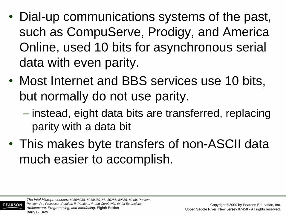
Copyright ©2009 by Pearson Education, Inc.
Upper Saddle River, New Jersey 07458 • All rights reserved.
The Intel Microprocessors: 8086/8088, 80186/80188, 80286, 80386, 80486 Pentium,
Pentium Pro Processor, Pentium II, Pentium, 4, and Core2 with 64-bit Extensions
Architecture, Programming, and Interfacing, Eighth Edition
Barry B. Brey
• Dial-up communications systems of the past,
such as CompuServe, Prodigy, and America
Online, used 10 bits for asynchronous serial
data with even parity.
• Most Internet and BBS services use 10 bits,
but normally do not use parity.
– instead, eight data bits are transferred, replacing
parity with a data bit
• This makes byte transfers of non-ASCII data
much easier to accomplish.

Copyright ©2009 by Pearson Education, Inc.
Upper Saddle River, New Jersey 07458 • All rights reserved.
The Intel Microprocessors: 8086/8088, 80186/80188, 80286, 80386, 80486 Pentium,
Pentium Pro Processor, Pentium II, Pentium, 4, and Core2 with 64-bit Extensions
Architecture, Programming, and Interfacing, Eighth Edition
Barry B. Brey
16550 Functional Description
• Fig 11–43 shows pin-outs of a 16550 UART.
• The device is available as a 40-pin DIP
(dual in-line package) or as a 44-pin PLCC
(plastic leadless chip carrier).
• Two completely separate sections are
responsible for data communications.
– the receiver and the transmitter
• Because each sections is independent, 16550
is able to function in simplex, half-duplex, or
full-duplex modes.

Copyright ©2009 by Pearson Education, Inc.
Upper Saddle River, New Jersey 07458 • All rights reserved.
The Intel Microprocessors: 8086/8088, 80186/80188, 80286, 80386, 80486 Pentium,
Pentium Pro Processor, Pentium II, Pentium, 4, and Core2 with 64-bit Extensions
Architecture, Programming, and Interfacing, Eighth Edition
Barry B. Brey
Figure 11–43 The pin-out of the 16550 UART.

Copyright ©2009 by Pearson Education, Inc.
Upper Saddle River, New Jersey 07458 • All rights reserved.
The Intel Microprocessors: 8086/8088, 80186/80188, 80286, 80386, 80486 Pentium,
Pentium Pro Processor, Pentium II, Pentium, 4, and Core2 with 64-bit Extensions
Architecture, Programming, and Interfacing, Eighth Edition
Barry B. Brey
• A major feature of the 16550 is its internal
receiver and transmitter FIFO (first-in, first-
out) memories.
• Because each is 16 bytes deep, the UART
requires attention from the processor only
after receiving 16 bytes of data.
– also holds 16 bytes before the processor
must wait for the transmitter
• The FIFO makes this UART ideal when
interfacing to high-speed systems because
less time is required to service it.

Copyright ©2009 by Pearson Education, Inc.
Upper Saddle River, New Jersey 07458 • All rights reserved.
The Intel Microprocessors: 8086/8088, 80186/80188, 80286, 80386, 80486 Pentium,
Pentium Pro Processor, Pentium II, Pentium, 4, and Core2 with 64-bit Extensions
Architecture, Programming, and Interfacing, Eighth Edition
Barry B. Brey
• A simplex system is one in which the
transmitter or receiver is used by itself.
– such as in an FM (frequency modulation)
radio station
• A half-duplex system is a CB (citizens
band) radio.
– transmit and receive, but not at the same time
• A full-duplex system allows transmission
and reception in both directions
simultaneously.
– the telephone is a full-duplex system

Copyright ©2009 by Pearson Education, Inc.
Upper Saddle River, New Jersey 07458 • All rights reserved.
The Intel Microprocessors: 8086/8088, 80186/80188, 80286, 80386, 80486 Pentium,
Pentium Pro Processor, Pentium II, Pentium, 4, and Core2 with 64-bit Extensions
Architecture, Programming, and Interfacing, Eighth Edition
Barry B. Brey
• The 16550 can control a modem
(modulator/demodulator), a device that
converts TTL serial data into audio tones
that can pass through the telephone system.
• Six pins on 16650 are for modem control:
DSR (data set ready), DTR (data terminal
ready), CTS (clear-to-send), RTS (request-
to-send), RI (ring indicator), and DCD (data
carrier detect).
• The modem is referred to as the data set and
the 16550 is referred to as the data terminal.

Copyright ©2009 by Pearson Education, Inc.
Upper Saddle River, New Jersey 07458 • All rights reserved.
The Intel Microprocessors: 8086/8088, 80186/80188, 80286, 80386, 80486 Pentium,
Pentium Pro Processor, Pentium II, Pentium, 4, and Core2 with 64-bit Extensions
Architecture, Programming, and Interfacing, Eighth Edition
Barry B. Brey
• The address inputs are used to select an
internal register for programming and also
data transfer.
• See Table 11–5 for a list of each
combination of the address inputs and
the registers selected.
16550 Pin Functions
A0, A1, A2
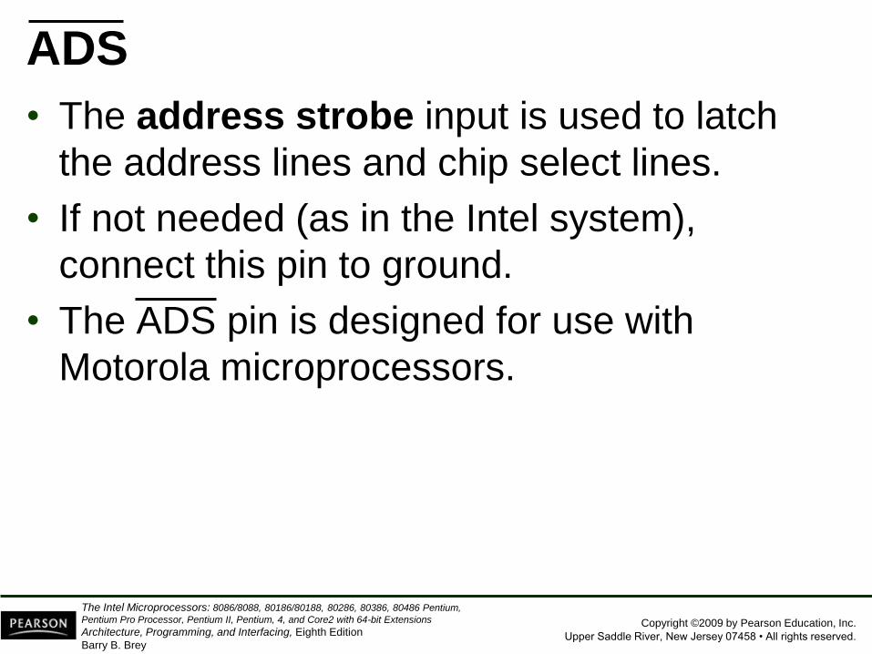
Copyright ©2009 by Pearson Education, Inc.
Upper Saddle River, New Jersey 07458 • All rights reserved.
The Intel Microprocessors: 8086/8088, 80186/80188, 80286, 80386, 80486 Pentium,
Pentium Pro Processor, Pentium II, Pentium, 4, and Core2 with 64-bit Extensions
Architecture, Programming, and Interfacing, Eighth Edition
Barry B. Brey
ADS
• The address strobe input is used to latch
the address lines and chip select lines.
• If not needed (as in the Intel system),
connect this pin to ground.
• The ADS pin is designed for use with
Motorola microprocessors.

Copyright ©2009 by Pearson Education, Inc.
Upper Saddle River, New Jersey 07458 • All rights reserved.
The Intel Microprocessors: 8086/8088, 80186/80188, 80286, 80386, 80486 Pentium,
Pentium Pro Processor, Pentium II, Pentium, 4, and Core2 with 64-bit Extensions
Architecture, Programming, and Interfacing, Eighth Edition
Barry B. Brey
BAUDOUT
• The baud out pin is where the clock signal
generated by the baud rate generator from
the transmitter section is made available.
• It is most often connected to the RCLK input
to generate a receiver clock that is equal to
the transmitter clock.
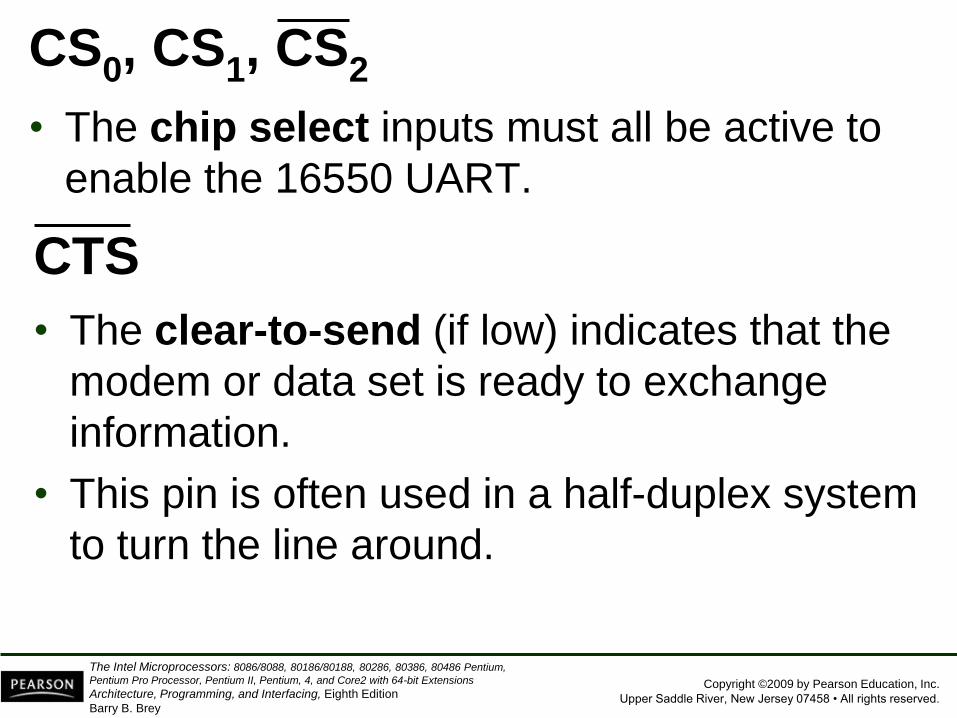
Copyright ©2009 by Pearson Education, Inc.
Upper Saddle River, New Jersey 07458 • All rights reserved.
The Intel Microprocessors: 8086/8088, 80186/80188, 80286, 80386, 80486 Pentium,
Pentium Pro Processor, Pentium II, Pentium, 4, and Core2 with 64-bit Extensions
Architecture, Programming, and Interfacing, Eighth Edition
Barry B. Brey
CS0, CS1, CS2
• The chip select inputs must all be active to
enable the 16550 UART.
CTS
• The clear-to-send (if low) indicates that the
modem or data set is ready to exchange
information.
• This pin is often used in a half-duplex system
to turn the line around.

Copyright ©2009 by Pearson Education, Inc.
Upper Saddle River, New Jersey 07458 • All rights reserved.
The Intel Microprocessors: 8086/8088, 80186/80188, 80286, 80386, 80486 Pentium,
Pentium Pro Processor, Pentium II, Pentium, 4, and Core2 with 64-bit Extensions
Architecture, Programming, and Interfacing, Eighth Edition
Barry B. Brey
D0–D7
• The data bus pins are connected to the
microprocessor data bus.
DCD
• Data carrier detect input is used by the
modem to signal the 16550 that a carrier
is present.

Copyright ©2009 by Pearson Education, Inc.
Upper Saddle River, New Jersey 07458 • All rights reserved.
The Intel Microprocessors: 8086/8088, 80186/80188, 80286, 80386, 80486 Pentium,
Pentium Pro Processor, Pentium II, Pentium, 4, and Core2 with 64-bit Extensions
Architecture, Programming, and Interfacing, Eighth Edition
Barry B. Brey
DTR
• Data terminal ready is an output that
indicates that the data terminal (16550)
is ready to function.
INTR
• Interrupt request is an output to the
microprocessor used to request an interrupt
(INTR=1) when the 16550 has a receiver
error, it has received data, and the
transmitter is empty.
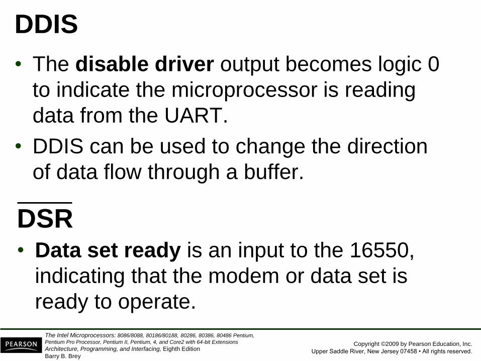
Copyright ©2009 by Pearson Education, Inc.
Upper Saddle River, New Jersey 07458 • All rights reserved.
The Intel Microprocessors: 8086/8088, 80186/80188, 80286, 80386, 80486 Pentium,
Pentium Pro Processor, Pentium II, Pentium, 4, and Core2 with 64-bit Extensions
Architecture, Programming, and Interfacing, Eighth Edition
Barry B. Brey
DDIS
• The disable driver output becomes logic 0
to indicate the microprocessor is reading
data from the UART.
• DDIS can be used to change the direction
of data flow through a buffer.
DSR • Data set ready is an input to the 16550,
indicating that the modem or data set is
ready to operate.
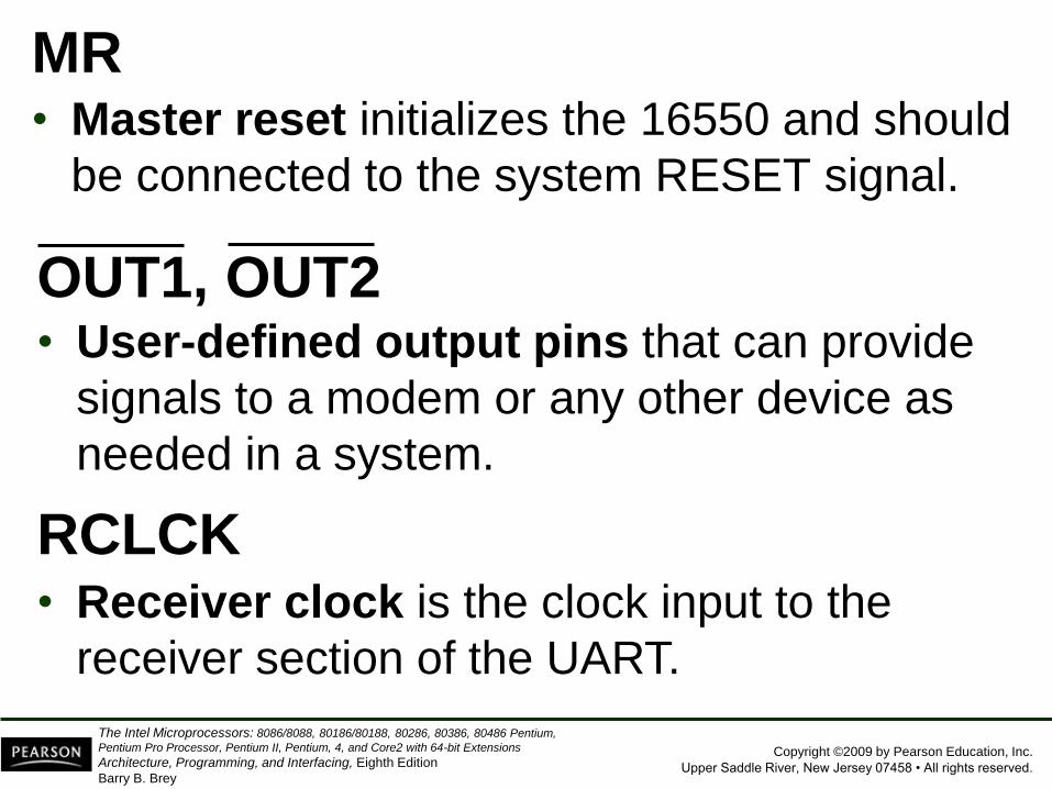
Copyright ©2009 by Pearson Education, Inc.
Upper Saddle River, New Jersey 07458 • All rights reserved.
The Intel Microprocessors: 8086/8088, 80186/80188, 80286, 80386, 80486 Pentium,
Pentium Pro Processor, Pentium II, Pentium, 4, and Core2 with 64-bit Extensions
Architecture, Programming, and Interfacing, Eighth Edition
Barry B. Brey
MR • Master reset initializes the 16550 and should
be connected to the system RESET signal.
OUT1, OUT2 • User-defined output pins that can provide
signals to a modem or any other device as
needed in a system.
RCLCK • Receiver clock is the clock input to the
receiver section of the UART.

Copyright ©2009 by Pearson Education, Inc.
Upper Saddle River, New Jersey 07458 • All rights reserved.
The Intel Microprocessors: 8086/8088, 80186/80188, 80286, 80386, 80486 Pentium,
Pentium Pro Processor, Pentium II, Pentium, 4, and Core2 with 64-bit Extensions
Architecture, Programming, and Interfacing, Eighth Edition
Barry B. Brey
RD, RD • Read inputs (either may be used) cause data
to be read from the register specified by the
address inputs to the UART.
RI • Ring indicator input is placed at logic 0 by
the modem to indicate the phone is ringing.
RTS • Request-to-send is a signal to the modem
indicating that the UART wishes to send data.

Copyright ©2009 by Pearson Education, Inc.
Upper Saddle River, New Jersey 07458 • All rights reserved.
The Intel Microprocessors: 8086/8088, 80186/80188, 80286, 80386, 80486 Pentium,
Pentium Pro Processor, Pentium II, Pentium, 4, and Core2 with 64-bit Extensions
Architecture, Programming, and Interfacing, Eighth Edition
Barry B. Brey
SIN, SOUT • These are the serial data pins. SIN accepts
serial data and SOUT transmits serial data.
RXRDY • Receiver ready is a signal used to transfer
received data via DMA techniques.
TXRDY • Transmitter ready is a signal used to
transfer transmitter data via DMA.

Copyright ©2009 by Pearson Education, Inc.
Upper Saddle River, New Jersey 07458 • All rights reserved.
The Intel Microprocessors: 8086/8088, 80186/80188, 80286, 80386, 80486 Pentium,
Pentium Pro Processor, Pentium II, Pentium, 4, and Core2 with 64-bit Extensions
Architecture, Programming, and Interfacing, Eighth Edition
Barry B. Brey
WR, WR • Write (either may be used) connects to the
microprocessor write signal to transfer
commands and data to the 16550.
XIN, XOUT • These are the main clock connections.
• A crystal is connected across these pins to
form a crystal oscillator, or XIN is connected
to an external timing source.

Copyright ©2009 by Pearson Education, Inc.
Upper Saddle River, New Jersey 07458 • All rights reserved.
The Intel Microprocessors: 8086/8088, 80186/80188, 80286, 80386, 80486 Pentium,
Pentium Pro Processor, Pentium II, Pentium, 4, and Core2 with 64-bit Extensions
Architecture, Programming, and Interfacing, Eighth Edition
Barry B. Brey
Programming the 16550
• Programming is a two-part process & includes
the initialization dialog and operational dialog.
• In the PC, which uses the 16550 or its
programming equivalent, I/O port addresses
are decoded at 3F8H - 3FFH for COM port 0
and 2F8H - 2FFH for COM port 2.

Copyright ©2009 by Pearson Education, Inc.
Upper Saddle River, New Jersey 07458 • All rights reserved.
The Intel Microprocessors: 8086/8088, 80186/80188, 80286, 80386, 80486 Pentium,
Pentium Pro Processor, Pentium II, Pentium, 4, and Core2 with 64-bit Extensions
Architecture, Programming, and Interfacing, Eighth Edition
Barry B. Brey
Initializing the 16550
• Initialization dialog after a hardware or
software reset, consists of two parts:
– programming the line control register
– programming the baud rate generator
• The line control register selects the number
of data bits, stop bits, and parity (whether
even or odd, or if parity is sent as a 1 or a 0)
• Baud rate generator is programmed with a
divisor that determines the baud rate of the
transmitter section.
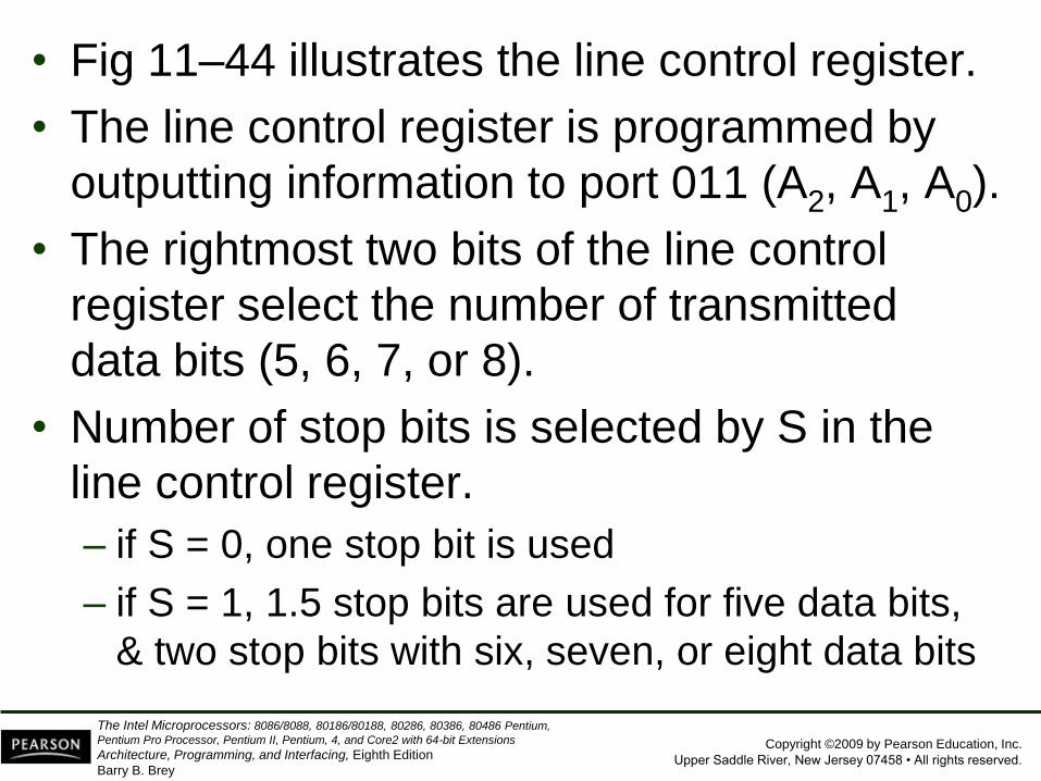
Copyright ©2009 by Pearson Education, Inc.
Upper Saddle River, New Jersey 07458 • All rights reserved.
The Intel Microprocessors: 8086/8088, 80186/80188, 80286, 80386, 80486 Pentium,
Pentium Pro Processor, Pentium II, Pentium, 4, and Core2 with 64-bit Extensions
Architecture, Programming, and Interfacing, Eighth Edition
Barry B. Brey
• Fig 11–44 illustrates the line control register.
• The line control register is programmed by
outputting information to port 011 (A2, A1, A0).
• The rightmost two bits of the line control
register select the number of transmitted
data bits (5, 6, 7, or 8).
• Number of stop bits is selected by S in the
line control register.
– if S = 0, one stop bit is used
– if S = 1, 1.5 stop bits are used for five data bits,
& two stop bits with six, seven, or eight data bits
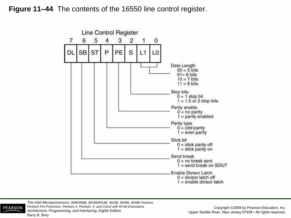
Copyright ©2009 by Pearson Education, Inc.
Upper Saddle River, New Jersey 07458 • All rights reserved.
The Intel Microprocessors: 8086/8088, 80186/80188, 80286, 80386, 80486 Pentium,
Pentium Pro Processor, Pentium II, Pentium, 4, and Core2 with 64-bit Extensions
Architecture, Programming, and Interfacing, Eighth Edition
Barry B. Brey
Figure 11–44 The contents of the 16550 line control register.

Copyright ©2009 by Pearson Education, Inc.
Upper Saddle River, New Jersey 07458 • All rights reserved.
The Intel Microprocessors: 8086/8088, 80186/80188, 80286, 80386, 80486 Pentium,
Pentium Pro Processor, Pentium II, Pentium, 4, and Core2 with 64-bit Extensions
Architecture, Programming, and Interfacing, Eighth Edition
Barry B. Brey
Programming the Baud Rate
• The baud rate generator is programmed at
I/O addresses 000 and 001 (A2, A1, A0).
• Port 000 is used to hold the least significant
part of the 16-bit divisor and port 001 is used
to hold the most significant part.
– value used for the divisor depends on the
external clock or crystal frequency
• Table 11–7 illustrates common baud rates
obtainable if an 18.432 MHz crystal is used
as a timing source.

Copyright ©2009 by Pearson Education, Inc.
Upper Saddle River, New Jersey 07458 • All rights reserved.
The Intel Microprocessors: 8086/8088, 80186/80188, 80286, 80386, 80486 Pentium,
Pentium Pro Processor, Pentium II, Pentium, 4, and Core2 with 64-bit Extensions
Architecture, Programming, and Interfacing, Eighth Edition
Barry B. Brey
Sample Initialization
• Suppose an asynchronous system requires
seven data bits, odd parity a baud rate of
9600, and one stop bit.
• Example 11–24 lists a procedure to initialize
the 16550 to function in this manner.
• Fig 11–45 shows the interface to the 8088
microprocessor, using a PLD to decode the
8-bit port addresses F0H through F7H.

Copyright ©2009 by Pearson Education, Inc.
Upper Saddle River, New Jersey 07458 • All rights reserved.
The Intel Microprocessors: 8086/8088, 80186/80188, 80286, 80386, 80486 Pentium,
Pentium Pro Processor, Pentium II, Pentium, 4, and Core2 with 64-bit Extensions
Architecture, Programming, and Interfacing, Eighth Edition
Barry B. Brey
Figure 11–45 The 16550 interfaced to the 8088 microprocessor at ports 00F0H–
00F7H.
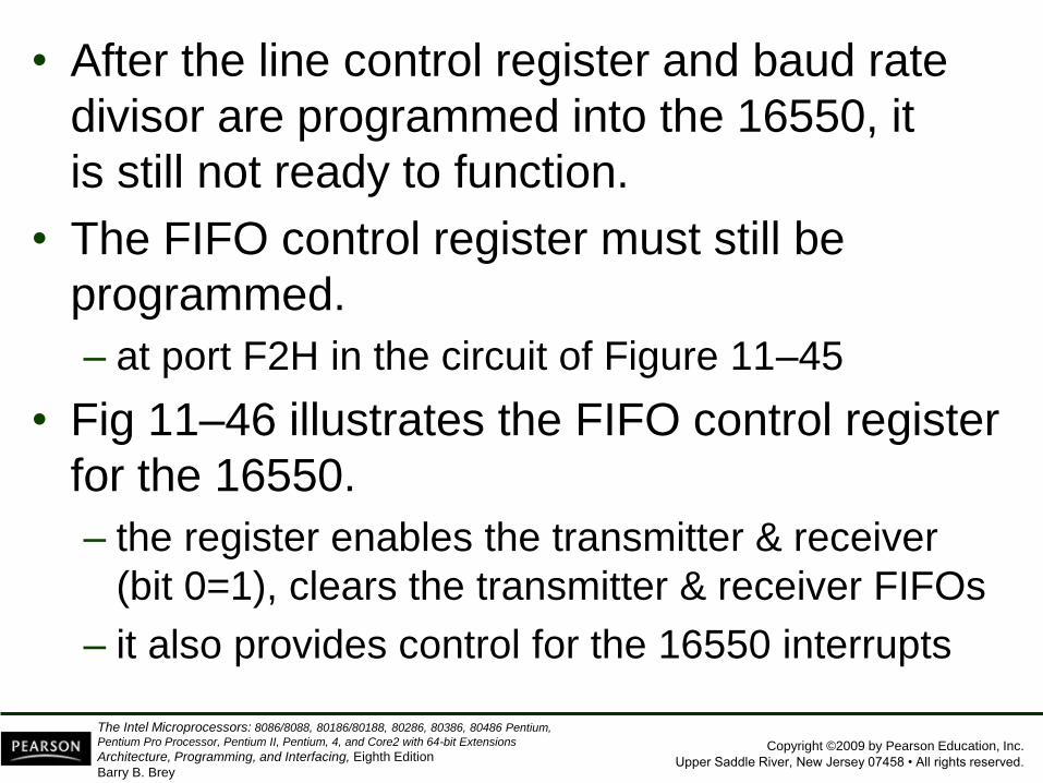
Copyright ©2009 by Pearson Education, Inc.
Upper Saddle River, New Jersey 07458 • All rights reserved.
The Intel Microprocessors: 8086/8088, 80186/80188, 80286, 80386, 80486 Pentium,
Pentium Pro Processor, Pentium II, Pentium, 4, and Core2 with 64-bit Extensions
Architecture, Programming, and Interfacing, Eighth Edition
Barry B. Brey
• After the line control register and baud rate
divisor are programmed into the 16550, it
is still not ready to function.
• The FIFO control register must still be
programmed.
– at port F2H in the circuit of Figure 11–45
• Fig 11–46 illustrates the FIFO control register
for the 16550.
– the register enables the transmitter & receiver
(bit 0=1), clears the transmitter & receiver FIFOs
– it also provides control for the 16550 interrupts

Copyright ©2009 by Pearson Education, Inc.
Upper Saddle River, New Jersey 07458 • All rights reserved.
The Intel Microprocessors: 8086/8088, 80186/80188, 80286, 80386, 80486 Pentium,
Pentium Pro Processor, Pentium II, Pentium, 4, and Core2 with 64-bit Extensions
Architecture, Programming, and Interfacing, Eighth Edition
Barry B. Brey
Figure 11–46 The FIFO control register of the 16550 UART.

Copyright ©2009 by Pearson Education, Inc.
Upper Saddle River, New Jersey 07458 • All rights reserved.
The Intel Microprocessors: 8086/8088, 80186/80188, 80286, 80386, 80486 Pentium,
Pentium Pro Processor, Pentium II, Pentium, 4, and Core2 with 64-bit Extensions
Architecture, Programming, and Interfacing, Eighth Edition
Barry B. Brey
• The last section of Example 11–26 places a
7 into the FIFO control register.
• This enables the transmitter and receiver,
and clears both FIFOs.
• The 16550 is now ready to operate, but
without interrupts.
– interrupts are automatically disabled when
the MR (master reset) input is placed at logic 1
by the system RESET signal.

Copyright ©2009 by Pearson Education, Inc.
Upper Saddle River, New Jersey 07458 • All rights reserved.
The Intel Microprocessors: 8086/8088, 80186/80188, 80286, 80386, 80486 Pentium,
Pentium Pro Processor, Pentium II, Pentium, 4, and Core2 with 64-bit Extensions
Architecture, Programming, and Interfacing, Eighth Edition
Barry B. Brey
Sending Serial Data
• Before serial data can be sent or received,
we need to know the function of the line
status register
– see Figure 11–47
• The line status register contains information
about error conditions and the state of the
transmitter and receiver.
• This register is tested before a byte is
transmitted or can be received.

Copyright ©2009 by Pearson Education, Inc.
Upper Saddle River, New Jersey 07458 • All rights reserved.
The Intel Microprocessors: 8086/8088, 80186/80188, 80286, 80386, 80486 Pentium,
Pentium Pro Processor, Pentium II, Pentium, 4, and Core2 with 64-bit Extensions
Architecture, Programming, and Interfacing, Eighth Edition
Barry B. Brey
Figure 11–47 The contents of the line status register of the 16550 UART.

Copyright ©2009 by Pearson Education, Inc.
Upper Saddle River, New Jersey 07458 • All rights reserved.
The Intel Microprocessors: 8086/8088, 80186/80188, 80286, 80386, 80486 Pentium,
Pentium Pro Processor, Pentium II, Pentium, 4, and Core2 with 64-bit Extensions
Architecture, Programming, and Interfacing, Eighth Edition
Barry B. Brey
Receiving Serial Data
• To read received information from the 16550,
test the DR bit of the line status register.
– example 11–28 lists a procedure to test the DR
bit to decide if the 16550 has received any data
• Upon the reception of data, the procedure
tests for errors.
– if an error is detected, the procedure returns
with AL equal to an ASCII ‘?’
– if no error has occurred, the procedure returns
with AL equal to the received character
Copyright ©2009 by Pearson Education, Inc.
Upper Saddle River, New Jersey 07458 • All rights reserved.
The Intel Microprocessors: 8086/8088, 80186/80188, 80286, 80386, 80486 Pentium,
Pentium Pro Processor, Pentium II, Pentium, 4, and Core2 with 64-bit Extensions
Architecture, Programming, and Interfacing, Eighth Edition
Barry B. Brey
UART Errors
• Errors detected by 16550 are:
– parity, framing, and overrun errors
• These errors should not occur during
normal operation.
• A parity error indicates the received data
contain the wrong parity.
– if a parity error occurs, it indicates noise
was encountered during reception

Copyright ©2009 by Pearson Education, Inc.
Upper Saddle River, New Jersey 07458 • All rights reserved.
The Intel Microprocessors: 8086/8088, 80186/80188, 80286, 80386, 80486 Pentium,
Pentium Pro Processor, Pentium II, Pentium, 4, and Core2 with 64-bit Extensions
Architecture, Programming, and Interfacing, Eighth Edition
Barry B. Brey
• A framing error indicates the start and stop
bits are not in their proper places.
– occurs if the receiver is receiving data at
an incorrect baud rate
• An overrun error indicates data have
overrun the internal receiver FIFO buffer.
– occurs only if the software fails to read the data
from the UART before the receiver FIFO is full

Copyright ©2009 by Pearson Education, Inc.
Upper Saddle River, New Jersey 07458 • All rights reserved.
The Intel Microprocessors: 8086/8088, 80186/80188, 80286, 80386, 80486 Pentium,
Pentium Pro Processor, Pentium II, Pentium, 4, and Core2 with 64-bit Extensions
Architecture, Programming, and Interfacing, Eighth Edition
Barry B. Brey
11–6 ANALOG-TO-DIGITAL (ADC)
& DIGITAL-TO-ANALOG (DAC)
CONVERTERS
• These devices are used to interface the
microprocessor to the analog world.
• Many events monitored and controlled by
the microprocessor are analog events.
• These range from monitoring all forms of
events, even speech, to controlling motors
and like devices.

Copyright ©2009 by Pearson Education, Inc.
Upper Saddle River, New Jersey 07458 • All rights reserved.
The Intel Microprocessors: 8086/8088, 80186/80188, 80286, 80386, 80486 Pentium,
Pentium Pro Processor, Pentium II, Pentium, 4, and Core2 with 64-bit Extensions
Architecture, Programming, and Interfacing, Eighth Edition
Barry B. Brey
The DAC0830 Digital-to-Analog
Converter
• A fairly common and low-cost digital-to-analog
converter is the DAC0830.
– a product of National Semiconductor Corp
• An 8-bit converter that transforms an 8-bit
binary number into an analog voltage.
• Other converters are available that convert
from 10-, 12-, or 16-bit binary numbers into
analog voltages.

Copyright ©2009 by Pearson Education, Inc.
Upper Saddle River, New Jersey 07458 • All rights reserved.
The Intel Microprocessors: 8086/8088, 80186/80188, 80286, 80386, 80486 Pentium,
Pentium Pro Processor, Pentium II, Pentium, 4, and Core2 with 64-bit Extensions
Architecture, Programming, and Interfacing, Eighth Edition
Barry B. Brey
• The number of voltage steps generated by
the converter is equal to the number of
binary input combinations.
– an 8-bit converter generates 256 voltage levels
– a 10-bit converter generates 1024 levels
• The DAC0830 is a medium-speed converter
that transforms a digital input to an analog
output in approximately 1.0 µs.

Copyright ©2009 by Pearson Education, Inc.
Upper Saddle River, New Jersey 07458 • All rights reserved.
The Intel Microprocessors: 8086/8088, 80186/80188, 80286, 80386, 80486 Pentium,
Pentium Pro Processor, Pentium II, Pentium, 4, and Core2 with 64-bit Extensions
Architecture, Programming, and Interfacing, Eighth Edition
Barry B. Brey
• Figure 11–48 shows pin-outs of a DAC0830.
• The device has eight data bus connections
for the application of the digital input code.
• Analog outputs labeled IOUT1 & IOUT2 are
inputs to an external operational amplifier.
• Because this is an 8-bit converter, its output
step voltage is defined as –VREF (reference
voltage), divided by 255.
– the step voltage is often called the resolution
of the converter

Copyright ©2009 by Pearson Education, Inc.
Upper Saddle River, New Jersey 07458 • All rights reserved.
The Intel Microprocessors: 8086/8088, 80186/80188, 80286, 80386, 80486 Pentium,
Pentium Pro Processor, Pentium II, Pentium, 4, and Core2 with 64-bit Extensions
Architecture, Programming, and Interfacing, Eighth Edition
Barry B. Brey
Figure 11–48 The pin-out of the DAC0830 digital-to-analog converter.

Copyright ©2009 by Pearson Education, Inc.
Upper Saddle River, New Jersey 07458 • All rights reserved.
The Intel Microprocessors: 8086/8088, 80186/80188, 80286, 80386, 80486 Pentium,
Pentium Pro Processor, Pentium II, Pentium, 4, and Core2 with 64-bit Extensions
Architecture, Programming, and Interfacing, Eighth Edition
Barry B. Brey
Internal Structure of the DAC0830
• Fig 11–49 shows the internal structure.
• This device contains two internal registers.
– the first is a holding register
– the second connects to the R–2R internal
ladder converter
• The two latches allow one byte to be held
while another is converted.
• The first latch is often disabled and the
second for entering data into the converter.
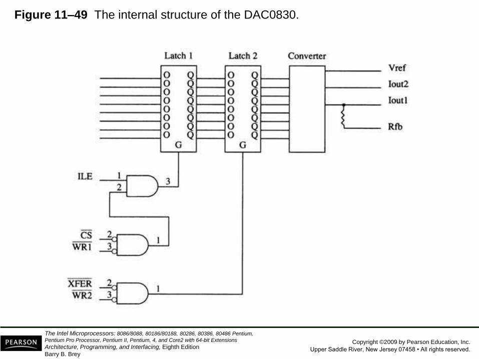
Copyright ©2009 by Pearson Education, Inc.
Upper Saddle River, New Jersey 07458 • All rights reserved.
The Intel Microprocessors: 8086/8088, 80186/80188, 80286, 80386, 80486 Pentium,
Pentium Pro Processor, Pentium II, Pentium, 4, and Core2 with 64-bit Extensions
Architecture, Programming, and Interfacing, Eighth Edition
Barry B. Brey
Figure 11–49 The internal structure of the DAC0830.

Copyright ©2009 by Pearson Education, Inc.
Upper Saddle River, New Jersey 07458 • All rights reserved.
The Intel Microprocessors: 8086/8088, 80186/80188, 80286, 80386, 80486 Pentium,
Pentium Pro Processor, Pentium II, Pentium, 4, and Core2 with 64-bit Extensions
Architecture, Programming, and Interfacing, Eighth Edition
Barry B. Brey
• Both latches within the DAC0830 are
transparent latches.
– when G input is logic 1, data pass through
– when G input becomes logic 0, data are latched
• The output of the R–2R ladder within the
converter appears at IOUT1 and IOUT2.
• These outputs are designed to be applied
to an operational amplifier such as a 741
or similar device.

Copyright ©2009 by Pearson Education, Inc.
Upper Saddle River, New Jersey 07458 • All rights reserved.
The Intel Microprocessors: 8086/8088, 80186/80188, 80286, 80386, 80486 Pentium,
Pentium Pro Processor, Pentium II, Pentium, 4, and Core2 with 64-bit Extensions
Architecture, Programming, and Interfacing, Eighth Edition
Barry B. Brey
Connecting the DAC0830 to the
Microprocessor.
• A PLD is used to decode the DAC0830 at I/O
port address 20H.
– when an OUT 20H,AL instruction is executed,
contents of data bus connections AD0–AD7 are
passed to the converter in the DAC0830
• The 741 operational amplifier, along with the –
12 V zener reference voltage, causes the full-
scale output voltage to equal +12 V.
• See Fig 11–50.

Copyright ©2009 by Pearson Education, Inc.
Upper Saddle River, New Jersey 07458 • All rights reserved.
The Intel Microprocessors: 8086/8088, 80186/80188, 80286, 80386, 80486 Pentium,
Pentium Pro Processor, Pentium II, Pentium, 4, and Core2 with 64-bit Extensions
Architecture, Programming, and Interfacing, Eighth Edition
Barry B. Brey
Figure 11–50 A DAC0830 interfaced to the 8086 microprocessor at 8-bit I/O location
20H.

Copyright ©2009 by Pearson Education, Inc.
Upper Saddle River, New Jersey 07458 • All rights reserved.
The Intel Microprocessors: 8086/8088, 80186/80188, 80286, 80386, 80486 Pentium,
Pentium Pro Processor, Pentium II, Pentium, 4, and Core2 with 64-bit Extensions
Architecture, Programming, and Interfacing, Eighth Edition
Barry B. Brey
The ADC080X Analog-to-Digital
Converter
• A common, low-cost ADC, compatible with a
wide range of microprocessors.
– while there are faster ADCs available with more
resolution, this device is ideal for applications
that do not require a high degree of accuracy
• ADC080X requires up to 100 µs to convert an
analog input voltage into a digital output code.
• Figure 11–51 shows the pin-out of the
ADC0804 converter.
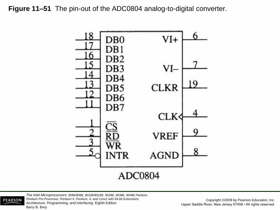
Copyright ©2009 by Pearson Education, Inc.
Upper Saddle River, New Jersey 07458 • All rights reserved.
The Intel Microprocessors: 8086/8088, 80186/80188, 80286, 80386, 80486 Pentium,
Pentium Pro Processor, Pentium II, Pentium, 4, and Core2 with 64-bit Extensions
Architecture, Programming, and Interfacing, Eighth Edition
Barry B. Brey
Figure 11–51 The pin-out of the ADC0804 analog-to-digital converter.

Copyright ©2009 by Pearson Education, Inc.
Upper Saddle River, New Jersey 07458 • All rights reserved.
The Intel Microprocessors: 8086/8088, 80186/80188, 80286, 80386, 80486 Pentium,
Pentium Pro Processor, Pentium II, Pentium, 4, and Core2 with 64-bit Extensions
Architecture, Programming, and Interfacing, Eighth Edition
Barry B. Brey
• To operate the converter, the WR pin is
pulsed with CS grounded to start the
conversion process.
• See Fig 11–52 for a timing diagram that
shows the interaction of the control signals.
• If a time delay is used that allows at least 100
µs of time, there is no need to test INTR pin.
• Another option is to connect the INTR pin to
an interrupt input, so when the conversion is
complete, an interrupt occurs.

Copyright ©2009 by Pearson Education, Inc.
Upper Saddle River, New Jersey 07458 • All rights reserved.
The Intel Microprocessors: 8086/8088, 80186/80188, 80286, 80386, 80486 Pentium,
Pentium Pro Processor, Pentium II, Pentium, 4, and Core2 with 64-bit Extensions
Architecture, Programming, and Interfacing, Eighth Edition
Barry B. Brey
Figure 11–52 The timing diagram for the ADC0804 analog-to-digital converter.

Copyright ©2009 by Pearson Education, Inc.
Upper Saddle River, New Jersey 07458 • All rights reserved.
The Intel Microprocessors: 8086/8088, 80186/80188, 80286, 80386, 80486 Pentium,
Pentium Pro Processor, Pentium II, Pentium, 4, and Core2 with 64-bit Extensions
Architecture, Programming, and Interfacing, Eighth Edition
Barry B. Brey
The Analog Input Signal
• Before ADC0804 can be connected, the two
analog inputs must be understood:
– VIN(+) and VIN(–)
• These differential inputs are summed by the
operational amplifier to produce a signal for
the internal analog-to-digital converter.
• These inputs are connected to an internal
operational amplifier as shown in Fig 11–53.

Copyright ©2009 by Pearson Education, Inc.
Upper Saddle River, New Jersey 07458 • All rights reserved.
The Intel Microprocessors: 8086/8088, 80186/80188, 80286, 80386, 80486 Pentium,
Pentium Pro Processor, Pentium II, Pentium, 4, and Core2 with 64-bit Extensions
Architecture, Programming, and Interfacing, Eighth Edition
Barry B. Brey
Figure 11–53 The analog inputs to the ADC0804 converter. (a) To sense a 0- to +5.0
V input. (b) To sense an input offset from ground.

Copyright ©2009 by Pearson Education, Inc.
Upper Saddle River, New Jersey 07458 • All rights reserved.
The Intel Microprocessors: 8086/8088, 80186/80188, 80286, 80386, 80486 Pentium,
Pentium Pro Processor, Pentium II, Pentium, 4, and Core2 with 64-bit Extensions
Architecture, Programming, and Interfacing, Eighth Edition
Barry B. Brey
Generating the Clock Signal
• ADC0804 requires a clock source to operate.
• It can be an external clock applied to CLK IN
pin or can be generated with an RC circuit.
– permissible range of clock frequencies is
100 KHz - 1460 KHz.
– desirable to use a frequency as close as possible
to 1460 KHz so conversion time is minimized
• If generated with an RC circuit, CLK IN and
CLK R pins are connected to an RC circuit,
as illustrated in Figure 11–54.

Copyright ©2009 by Pearson Education, Inc.
Upper Saddle River, New Jersey 07458 • All rights reserved.
The Intel Microprocessors: 8086/8088, 80186/80188, 80286, 80386, 80486 Pentium,
Pentium Pro Processor, Pentium II, Pentium, 4, and Core2 with 64-bit Extensions
Architecture, Programming, and Interfacing, Eighth Edition
Barry B. Brey
Figure 11–54 Connecting the RC circuit to the CLK IN and CLK R pins on the
ADC0804.

Copyright ©2009 by Pearson Education, Inc.
Upper Saddle River, New Jersey 07458 • All rights reserved.
The Intel Microprocessors: 8086/8088, 80186/80188, 80286, 80386, 80486 Pentium,
Pentium Pro Processor, Pentium II, Pentium, 4, and Core2 with 64-bit Extensions
Architecture, Programming, and Interfacing, Eighth Edition
Barry B. Brey
Connecting the ADC0804 to the
Microprocessor
• ADC0804 interfaced to an 8086 is illustrated
in Figure 11–55.
– VREF is not attached to anything, which is normal
• Suppose ADC0804 is decoded at I/O port
address 40H for the data and address 42H
for INTR.
• The procedure to read data is listed in
Example 11–29.

Copyright ©2009 by Pearson Education, Inc.
Upper Saddle River, New Jersey 07458 • All rights reserved.
The Intel Microprocessors: 8086/8088, 80186/80188, 80286, 80386, 80486 Pentium,
Pentium Pro Processor, Pentium II, Pentium, 4, and Core2 with 64-bit Extensions
Architecture, Programming, and Interfacing, Eighth Edition
Barry B. Brey
Figure 11–55 The ADC0804 interfaced to the 8086 microprocessor.

Copyright ©2009 by Pearson Education, Inc.
Upper Saddle River, New Jersey 07458 • All rights reserved.
The Intel Microprocessors: 8086/8088, 80186/80188, 80286, 80386, 80486 Pentium,
Pentium Pro Processor, Pentium II, Pentium, 4, and Core2 with 64-bit Extensions
Architecture, Programming, and Interfacing, Eighth Edition
Barry B. Brey
Using the ADC0804 and the
DAC0830
• This illustrates an example using an ADC0804
and a DAC0830 to capture and replay audio
signals or speech.
– a speech synthesizer has been used in the past
to generate speech, but quality was poor
• For human quality speech, we can use an
ADC0804 to capture an audio signal and
store it for later playback through a DAC0830.

Copyright ©2009 by Pearson Education, Inc.
Upper Saddle River, New Jersey 07458 • All rights reserved.
The Intel Microprocessors: 8086/8088, 80186/80188, 80286, 80386, 80486 Pentium,
Pentium Pro Processor, Pentium II, Pentium, 4, and Core2 with 64-bit Extensions
Architecture, Programming, and Interfacing, Eighth Edition
Barry B. Brey
• Fig 11–56 shows circuitry required to connect
the ADC0804 at I/O ports 0700H and 0702H.
• The DAC0830 is interfaced at I/O port 704H.
– These ports are in the low bank of a 16-bit
microprocessor such as the 8086/80386SX
• The software appears in Example 11–30.
• It reads a 1-second burst of speech and
plays it back 10 times.

Copyright ©2009 by Pearson Education, Inc.
Upper Saddle River, New Jersey 07458 • All rights reserved.
The Intel Microprocessors: 8086/8088, 80186/80188, 80286, 80386, 80486 Pentium,
Pentium Pro Processor, Pentium II, Pentium, 4, and Core2 with 64-bit Extensions
Architecture, Programming, and Interfacing, Eighth Edition
Barry B. Brey
Figure 11–56 A circuit that stores speech and plays it back through the speaker.

Copyright ©2009 by Pearson Education, Inc.
Upper Saddle River, New Jersey 07458 • All rights reserved.
The Intel Microprocessors: 8086/8088, 80186/80188, 80286, 80386, 80486 Pentium,
Pentium Pro Processor, Pentium II, Pentium, 4, and Core2 with 64-bit Extensions
Architecture, Programming, and Interfacing, Eighth Edition
Barry B. Brey
• A procedure called READS reads the speech.
• A second, PLAYS, plays it back.
• The speech is sampled and stored in a
section of memory called WORDS.
• The sample rate is chosen at 2048 samples
per second, which renders acceptable-
sounding speech.

Copyright ©2009 by Pearson Education, Inc.
Upper Saddle River, New Jersey 07458 • All rights reserved.
The Intel Microprocessors: 8086/8088, 80186/80188, 80286, 80386, 80486 Pentium,
Pentium Pro Processor, Pentium II, Pentium, 4, and Core2 with 64-bit Extensions
Architecture, Programming, and Interfacing, Eighth Edition
Barry B. Brey
SUMMARY
• The 8086-Core2 microprocessors have two
basic types of I/O instructions: IN and OUT.
• The IN instruction inputs data from an
external I/O device into either the AL (8-bit)
or AX (16-bit) register.
• The IN instruction is available as a fixed
port instruction, a variable port instruction,
or a string instruction (80286-Pentium 4)
INSB or INSW.
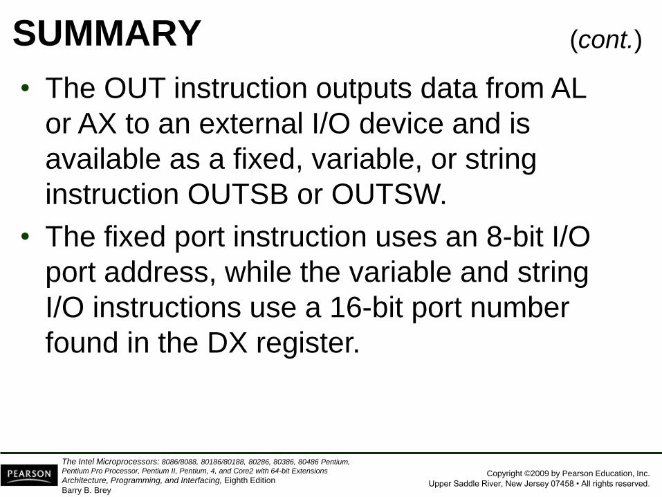
Copyright ©2009 by Pearson Education, Inc.
Upper Saddle River, New Jersey 07458 • All rights reserved.
The Intel Microprocessors: 8086/8088, 80186/80188, 80286, 80386, 80486 Pentium,
Pentium Pro Processor, Pentium II, Pentium, 4, and Core2 with 64-bit Extensions
Architecture, Programming, and Interfacing, Eighth Edition
Barry B. Brey
SUMMARY
• The OUT instruction outputs data from AL
or AX to an external I/O device and is
available as a fixed, variable, or string
instruction OUTSB or OUTSW.
• The fixed port instruction uses an 8-bit I/O
port address, while the variable and string
I/O instructions use a 16-bit port number
found in the DX register.
(cont.)
Copyright ©2009 by Pearson Education, Inc.
Upper Saddle River, New Jersey 07458 • All rights reserved.
The Intel Microprocessors: 8086/8088, 80186/80188, 80286, 80386, 80486 Pentium,
Pentium Pro Processor, Pentium II, Pentium, 4, and Core2 with 64-bit Extensions
Architecture, Programming, and Interfacing, Eighth Edition
Barry B. Brey
SUMMARY
• Isolated I/O, sometimes called direct I/O,
uses a separate map for the I/O space,
freeing the entire memory for use by the
program.
• Isolated I/O uses the IN and OUT
instructions to transfer data between the I/O
device and the micro-processor.
(cont.)

Copyright ©2009 by Pearson Education, Inc.
Upper Saddle River, New Jersey 07458 • All rights reserved.
The Intel Microprocessors: 8086/8088, 80186/80188, 80286, 80386, 80486 Pentium,
Pentium Pro Processor, Pentium II, Pentium, 4, and Core2 with 64-bit Extensions
Architecture, Programming, and Interfacing, Eighth Edition
Barry B. Brey
SUMMARY
• Memory-mapped I/O uses a portion of the
memory space for I/O transfers.
• In addition, any instruction that addresses a
memory location using any addressing
mode can be used to transfer data between
the microprocessor and the I/O device
using memory-mapped I/O.
(cont.)

Copyright ©2009 by Pearson Education, Inc.
Upper Saddle River, New Jersey 07458 • All rights reserved.
The Intel Microprocessors: 8086/8088, 80186/80188, 80286, 80386, 80486 Pentium,
Pentium Pro Processor, Pentium II, Pentium, 4, and Core2 with 64-bit Extensions
Architecture, Programming, and Interfacing, Eighth Edition
Barry B. Brey
SUMMARY
• All input devices are buffered so that the I/O
data are connected only to the data bus
during the execution of the IN instruction.
• The buffer is either built into a
programmable peripheral or located
separately.
• All output devices use a latch to capture
output data during the execution of the OUT
instruction.
(cont.)
Copyright ©2009 by Pearson Education, Inc.
Upper Saddle River, New Jersey 07458 • All rights reserved.
The Intel Microprocessors: 8086/8088, 80186/80188, 80286, 80386, 80486 Pentium,
Pentium Pro Processor, Pentium II, Pentium, 4, and Core2 with 64-bit Extensions
Architecture, Programming, and Interfacing, Eighth Edition
Barry B. Brey
SUMMARY
• Handshaking or polling is the act of two
independent devices synchronizing with a
few control lines.
• This communication between the computer
and the printer is a handshake or a poll.
• Interfaces are required for most switch-
based input devices and for most output
devices that are not TTL-compatible.
(cont.)

Copyright ©2009 by Pearson Education, Inc.
Upper Saddle River, New Jersey 07458 • All rights reserved.
The Intel Microprocessors: 8086/8088, 80186/80188, 80286, 80386, 80486 Pentium,
Pentium Pro Processor, Pentium II, Pentium, 4, and Core2 with 64-bit Extensions
Architecture, Programming, and Interfacing, Eighth Edition
Barry B. Brey
SUMMARY
• The I/O port number appears on address
bus connections A7-A0 for a fixed port I/O
instruction and on A15-A0 for a variable
port I/O instruction (note that A15-A8
contains zeros for an 8-bit port).
• In both cases, address bits above A15 are
undefined.
(cont.)

Copyright ©2009 by Pearson Education, Inc.
Upper Saddle River, New Jersey 07458 • All rights reserved.
The Intel Microprocessors: 8086/8088, 80186/80188, 80286, 80386, 80486 Pentium,
Pentium Pro Processor, Pentium II, Pentium, 4, and Core2 with 64-bit Extensions
Architecture, Programming, and Interfacing, Eighth Edition
Barry B. Brey
SUMMARY
• Because the 8086/80286/80386SX
microprocessors contain a 16-bit data bus
and the I/O addresses reference byte-sized
I/O locations, I/O space is also organized in
banks, as is the memory system.
• In order to interface an 8-bit I/O device to
the 16-bit data bus, we often require
separate write strobes (an upper and a
lower) for I/O write operations.
(cont.)

Copyright ©2009 by Pearson Education, Inc.
Upper Saddle River, New Jersey 07458 • All rights reserved.
The Intel Microprocessors: 8086/8088, 80186/80188, 80286, 80386, 80486 Pentium,
Pentium Pro Processor, Pentium II, Pentium, 4, and Core2 with 64-bit Extensions
Architecture, Programming, and Interfacing, Eighth Edition
Barry B. Brey
SUMMARY
• The I/O port decoder is much like the
memory address decoder, except instead of
decoding the entire address, the I/O port
decoder decodes only a 16-bit address for
variable port instructions and often an 8-bit
port number for fixed I/O instructions.
• The 82C55 is a programmable peripheral
interface (PIA) that has 24 I/O pins that are
programmable in two groups of 12 pins
each (group A and group B).
(cont.)

Copyright ©2009 by Pearson Education, Inc.
Upper Saddle River, New Jersey 07458 • All rights reserved.
The Intel Microprocessors: 8086/8088, 80186/80188, 80286, 80386, 80486 Pentium,
Pentium Pro Processor, Pentium II, Pentium, 4, and Core2 with 64-bit Extensions
Architecture, Programming, and Interfacing, Eighth Edition
Barry B. Brey
SUMMARY
• The 82C55 operates in three modes: simple
I/O (mode 0), strobed I/O (mode 1), and
bidirectional I/O (mode 2).
• When the 82C55 is interfaced to the 8086
operating at 8 MHz, we insert two wait
states because the speed of is faster than
the 82C55 can handle.
• The LCD display device requires a fair
amount of software, but it displays AS-CII-
coded information.
(cont.)
Copyright ©2009 by Pearson Education, Inc.
Upper Saddle River, New Jersey 07458 • All rights reserved.
The Intel Microprocessors: 8086/8088, 80186/80188, 80286, 80386, 80486 Pentium,
Pentium Pro Processor, Pentium II, Pentium, 4, and Core2 with 64-bit Extensions
Architecture, Programming, and Interfacing, Eighth Edition
Barry B. Brey
SUMMARY
• The 8254 is a programmable interval timer
with three 16-bit counters that count in
binary or binary-coded decimal (BCD).
• Each counter is independent and operates
in six different modes: (1) events counter,
(2) retriggerable, monostable multivibrator,
(3) pulse generator, (4) square-wave
generator, (5) software-triggered pulse
generator, and (6) hardware-triggered pulse
generator.
(cont.)

Copyright ©2009 by Pearson Education, Inc.
Upper Saddle River, New Jersey 07458 • All rights reserved.
The Intel Microprocessors: 8086/8088, 80186/80188, 80286, 80386, 80486 Pentium,
Pentium Pro Processor, Pentium II, Pentium, 4, and Core2 with 64-bit Extensions
Architecture, Programming, and Interfacing, Eighth Edition
Barry B. Brey
SUMMARY
• The 16550 is a programmable
communications interface, capable of
receiving and transmitting asynchronous
serial data.
• The DAC0830 is an 8-bit digital-to-analog
converter that converts a digital signal to an
analog voltage within 1.0 µs.
• The ADC0804 is an 8-bit analog-to-digital
converter that converts an analog signal
into a digital signal within 100 µs.


![Designingenergyefficient’ microprocessor:Howtofight ... Memory ... [MHz] 8086 80286 386DX 486DX 486DX4 Pentium Pentium Pro Pentium II Pentium MMX Pentium III ... Delay buffers are](https://img.dokumen.tips/doc/110x75/5ac1a5637f8b9ac6688d9ef1/designingenergyecient-microprocessorhowtoght-memory-mhz-8086.jpg)


