Embed Size (px)
Citation preview
CChhaapptteerr 11 TTrraannssppaarreenntt CCoonndduuccttiinngg OOxxiiddeess

2
3
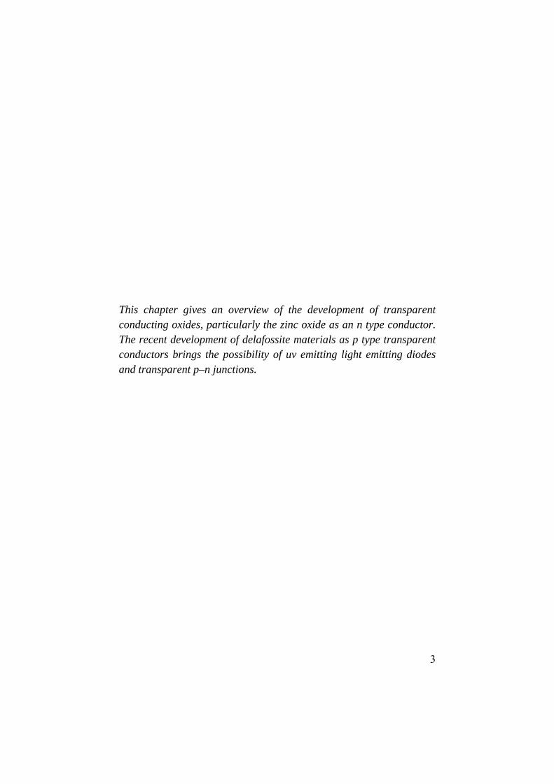
This chapter gives an overview of the development of transparent conducting oxides, particularly the zinc oxide as an n type conductor. The recent development of delafossite materials as p type transparent conductors brings the possibility of uv emitting light emitting diodes and transparent p–n junctions.

4
5
11..11 IInnttrroodduuccttiioonn Materials exhibiting transparency and electrical conductivity simultaneously, transparent conductors, have been the focus of frontier research ever since the first report of transparent conducting CdO films. [1] Transparent conducting oxides (TCOs), which have high transparency through the visible spectrum and high electrical conductivity are already being used in numerous applications. Low-emission windows that allow visible light through while reflecting the infrared, this keeps the heat out in summer, or the heat in, in winter. A thin conducting layer on or in between the glass panes achieves this. Low-emission windows use mostly F-doped SnO2. Most of these TCO’s are n type semiconductors and are utilized in a variety of commercial applications, such as flat-panel displays, photovoltaic devices, and electrochromic windows, in which they serve as transparent electrodes. Novel functions may be integrated into the materials since oxides have a variety of elements and crystal structures, providing great potential for realizing a diverse range of active functions. However, the application of TCOs has been restricted to transparent electrodes, notwithstanding the fact that TCOs are n-type semiconductors. The primary reason is the lack of p-type TCOs, because many of the active functions in semiconductors originate from the nature of the pn-junction. In 1997, H. Kawazoe et al.[2] reported CuAlO2 thin films as a first p-type TCO along with a chemical design concept for the exploration of other p-type TCOs. This has led to the fabrications of all oxide transparent diodes and transistors [3]. TCO’s are wide band gap materials that have relatively high concentration of carriers in the conduction band. These arise either from defects in the material or from extrinsic dopants, the impurity level of which lie near the conduction band edge. The high carrier concentration would cause absorption of electromagnetic radiation. Thus a TCO represents a compromise between electrical conductivity and optical transmission. Reduction of resistivity involves either increase in the carrier concentration or in their mobility. The mobility of typical semiconductor is about 40 cm2 V-1 s-1. Increasing the number of carriers leads to an increase in the
6
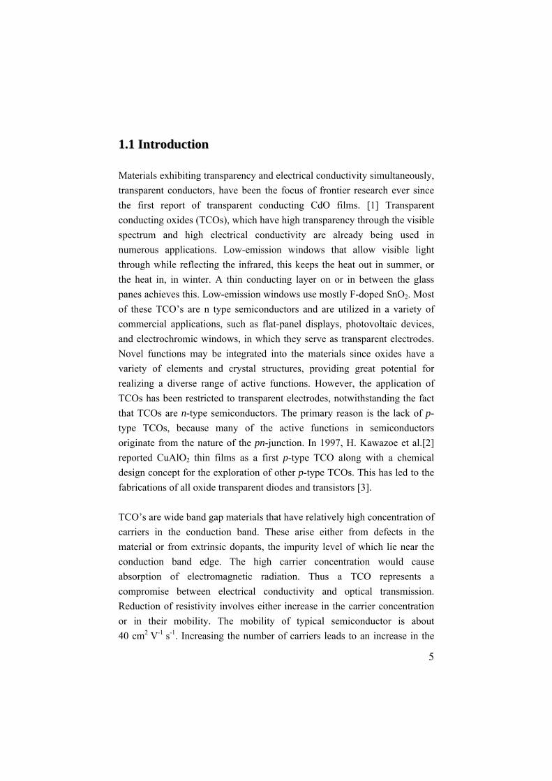
visible absorption while increasing the mobility has no negative effects on the figure of merit of the TCOs. Thus increasing the figure of merit of the TCOs essentially should aim to increase the mobility since this would increase the optical transmission and electrical conductivity The relationship between mobility and carrier density of semiconductors is shown in figure 1.1 [4] Conductivity is given by the relation
( )( )m
tne2=σ Ω-1cm-1 (1.1)
Where, n is the carrier density, e the electronic charge, t the thickness of the semiconductor and m the mass of the charge carriers.
Figure 1.1 Relationship between mobility and carrier density of semiconductors
7
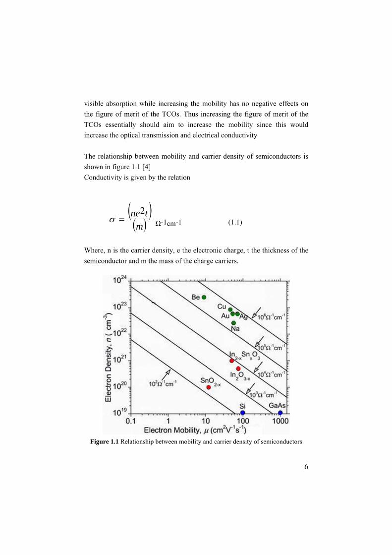
The lack of high-quality epitaxial or single-crystalline transparent oxide semiconductor films is another reason for their limited application. Although there have been many reports of the fabrication of transparent optoelectronic devices such as pn-junction diodes and transistors using transparent oxide semiconductors (TOSs), their performance is significantly inferior to III-V semiconductor devices because the thin films are polycrystalline, i.e. defects and grain boundaries in the active layer deteriorate the device performance. Optoelectronic properties and, therefore, device performance are expected to improve drastically by using single-crystalline or high-quality epitaxial film in place of nonoriented polycrystalline films [5]. The development of a high figure-of-merit p-type TCO would enable development of ultraviolet light emitting diodes, heterojunctions for solar cells, and all oxide transparent semiconductor devices such as diodes and transistors. 11..22 GGeenneerraall PPrrooppeerrttiieess OOff TTrraannssppaarreenntt CCoonndduuccttiinngg OOxxiiddeess 1.2.1 Theory of transparency and conductivity As far as the properties of a solid are concerned, one can see that optical transparency and electrical conductivity are antonyms to each other. This can be easily proved using the Maxwell’s equations of electromagnetic theory [6] as described below. For electromagnetic (em) waves passing through an uncharged semiconducting medium, the solution to Maxwell’s equation gives the real and complex parts of the refractive index as
⎥⎥⎥
⎦
⎤
⎢⎢⎢
⎣
⎡+
⎪⎭
⎪⎬⎫
⎪⎩
⎪⎨⎧
⎟⎠⎞
⎜⎝⎛+= 121
2
21
22
υσεn and
⎥⎥⎥
⎦
⎤
⎢⎢⎢
⎣
⎡−
⎪⎭
⎪⎬⎫
⎪⎩
⎪⎨⎧
⎟⎠⎞
⎜⎝⎛+= 121
2
21
22
υσεk (1.2)
8
where n is the refractive index of the medium, k is the extinction coefficient, ε is the dielectric constant, σ is the conductivity of the medium and ν is the frequency of the electromagnetic radiation. In the case of an insulator, where
0→σ , then 21
ε→n and 0→k . This implies that an insulator is transparent to electromagnetic waves. For a perfect conductor, the solution to the Maxwell’s equation yields, the reflected and transmitted component of the electric field vector as ER = -EI and ET = 0. This means that the wave is totally reflected with 1800 phase difference. In other words, a good conductor reflects the radiations incident on it, while a good insulator is transparent to the electromagnetic radiations. 1.2.2 Correlation of electrical and optical properties The optical phenomena in the IR range can be explained on the basis of Drude’s theory for free electrons in metals [7,8,9]. When the free electrons interact with an em field, it may lead to polarisation of the field within the material. It affects the relative permittivity ε. For an electron moving in an electric field, the equation of motion can be written as,
Ftv
dtdm =⎟
⎠⎞
⎜⎝⎛ + )(1 δ
τ (1.3)
where τ is the relaxation time . The force on an electron in an alternating field is given by F = -eE e -iωt (1.4)
Let us assume a solution to (1.4) in the form δv = δv e-iωt
Then (1.3) becomes,
eEvim −=⎟⎠⎞
⎜⎝⎛ +− δ
τω 1
or , ωτ
τδ
im
ev
−−=
1 (1.5)
9
The current density is
j = nqδv = ( ) Eim
neωττ
−1
2
,
where n is the electron concentration and q is the charge on the electron. The electrical conductivity is
( ) ( ) ( )20
2
11
1 ωτωτσ
ωττωσ
++
=−
=i
imne (1.6)
Here, σ0 = ne2τ / m is the dc conductivity. At high frequencies, ωτ >>1, we can write,
( )( ) ωτωωτωτ
σωσmnei
mnei 2
2
2
201
+=⎟⎟⎠
⎞⎜⎜⎝
⎛+=
In this equation the imaginary term is dominant and is independent of τ. Thus we can express the result as a complex dielectric constant instead of expressing it as a complex conductivity.
The dielectric constant ε = 1+ ( 4πP/E)
where Eim
neP
τωω +
−=2
2
Then, ( )τ
ωω
πωε
im
ne
+−=
2
241 ( 1.7)
This expression gives the dielectric constant of a free electron gas. For ∞→τ the dielectric constant is positive and real if m
ne22 4πω > .
Electromagnetic wave cannot propagate in a medium with negative dielectric constant because then wave vector is imaginary and the wave decays exponentially. Waves incident on such a medium are totally reflected. We
can denote the cut off frequency as ( ) 2124
mne
pπω = this is known as the
10
plasma frequency. The material is transparent to the em radiation whose frequency is greater than the plasma frequency. 1.2.3 Electrical properties Numerous investigations have been made on the electrical properties of transparent conducting oxide films to understand the conduction phenomena [10,11]. Researchers have made a systematic study on the effect of various parameters such as nature of substrate, substrate temperature, film thickness, dopant and its concentration etc [12,13] on the electrical properties of TCO films. The high conductivity of the TCO films results mainly from non stoichiometry. The conduction electrons in these films are supplied from donor sites associated with oxygen vacancies or excess metal ions[14]. These donor sites can be easily created by chemical reduction. Unintentional doping(which happens mainly in the case of film deposition by spray pyrolysis), intentional doping and contamination by alkali ions from the glass substrate can affect electrical conductivity. One of the major factor governing the conductivity of TCO films is the carrier mobility. The mobility of the carriers in the polycrystalline film is dependent on the mechanism by which carriers are scattered by lattice imperfections. The various scattering mechanisms involved in semiconducting thin films are acoustic deformation potential scattering [15], piezoelectric scattering [16], optical phonon scattering [17] neutral impurity scattering [18], ionized impurity scattering [19], electron-electron scattering [20] and grain boundary scattering [21]. In the case of a polycrystalline film, the conduction mechanism is dominated by the inherent inter-crystalline boundaries rather than the intra-crystalline characteristics. These boundaries generally contain fairly high densities of interface states that trap free carriers by virtue of the inherent disorders and the presence of trapped charges. The interface states results in a space charge
11
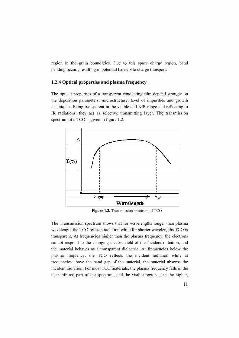
region in the grain boundaries. Due to this space charge region, band bending occurs, resulting in potential barriers to charge transport. 1.2.4 Optical properties and plasma frequency The optical properties of a transparent conducting film depend strongly on the deposition parameters, microstructure, level of impurities and growth techniques. Being transparent in the visible and NIR range and reflecting to IR radiations, they act as selective transmitting layer. The transmission spectrum of a TCO is given in figure 1.2.
Figure 1.2. Transmission spectrum of TCO
The Transmission spectrum shows that for wavelengths longer than plasma wavelength the TCO reflects radiation while for shorter wavelengths TCO is transparent. At frequencies higher than the plasma frequency, the electrons cannot respond to the changing electric field of the incident radiation, and the material behaves as a transparent dielectric. At frequencies below the plasma frequency, the TCO reflects the incident radiation while at frequencies above the band gap of the material, the material absorbs the incident radiation. For most TCO materials, the plasma frequency falls in the near-infrared part of the spectrum, and the visible region is in the higher,
12
transparent frequency range. The plasma frequency increases approximately with the square root of the conduction-electron concentration. The maximum obtainable electron concentration and the plasma frequency of TCOs generally increase in the same order as the resistivity[22].
1.2.5 Optical and Electrical Performance of Transparent Conductors TCOs have two important qualities with which they can be judged, optical transmission and electrical conductivity, and these two parameters are somewhat inversely related, a method of comparing the properties of these films is essential. Figure of merit have allowed researchers to compare the various results in a reasonable and direct manner. Researchers have developed different methods for finding the figures of merit of the films. One of the earliest equations defining a figure of merit was developed by
Fraser and Cook[23] and is given by the relation s
FC RTF = where T is the
transmission and Rs is the sheet resistance of the thin film. This value was often multiplied by 1000 to allow comparisons of numbers greater than one. This definition depends on the film thickness.
Another definition for figure of merit, FH, developed by Haacke [24] is also related to the above definition. However, FH puts more emphasis on the optical transparency because FFC was too much in favor of sheet resistance, resulting in a maximum figure of merit at relatively large film thicknesses.
The figure of merit was redefined as s
xa
H RT
F = where x>1. Haacke selected
the value of x = 10. The definition by Haacke is also thickness dependent.
13
The third definition for figure of merit was developed by Iles and Soclof [25]. A figure of merit that is independent of film thickness is given by
[ ]σα
=−= TRF ss 11
By this definition, a lower value of figure of merit indicates films of better quality.
Most of the variation in the figure of merit of TCO is due to differences in mobility, but the free-electron concentration does not affect the figure of merit. The electron mobility is determined by the electron-scattering mechanisms that operate in the material. First of all, some scattering mechanisms, such as scattering of electrons by phonons, are present in pure single crystals. Practical TCOs need much higher doping levels and for these high doping levels, scattering by the ionised dopant atoms become another important mechanism that alone limits the mobility. This maximum mobility is lowered still further by other scattering mechanisms such as grain-boundary scattering, present in polycrystalline thin films. The best TCO films, ZnO:F and Cd2SnO4, have been prepared with mobilities in the range of 50–60 cm2 V_1 s_1[26]. 1.2.6 Work Function The work function of a TCO is defined as the minimum energy required to remove an electron from the fermi level to the vacuum level. ZnO has a work function of 4.57eV [27]. 1.2.7 Thermal Stability of Transparent Conductors TCOs will generally will have an increase in resistivity if heated to a high enough temperature for a long enough time. TCOs remains stable to temperatures slightly above the optimised deposition temperature.
14
1.2.8 Minimum Deposition Temperature The substrate temperature, during deposition of TCO thin films, must be at a sufficiently high in order to develop the required properties for the TCO. The required temperatures are usually found to increase in the following order: ITO<ZnO<SnO2<Cd2SnO4 [10]. ITO is preferred for deposition on thermally sensitive substrates, such as plastic, while cadmium stannate requires highly refractory substrates to achieve its best properties. 1.2.9 Diffusion Barriers between Transparent Conductors and Sodium-Containing Glass Substrates When TCOs are deposited on sodium containing glass, such as soda-lime glass, sodium can diffuse into the TCO and increase its resistance. This effect is particularly noticeable for tin oxide, because sodium diffuses rapidly at the high substrate temperatures (often 5500C) used for its deposition. It is common to deposit a barrier layer on the glass prior to the deposition of tin oxide. Silica or alumina is used commonly as the barrier layer between soda-lime glass and tin oxide.
1.2.10 Etching Patterns in TCOs For some applications of TCOs, such as displays, heaters, or antennas, parts of the TCO must be removed. Zinc oxide is the easiest material to etch, tin oxide is the most difficult, and indium oxide is intermediate in etching difficulty [10]. Series-connected thin-film solar cells need to remove TCOs along patterns of lines. This removal is usually carried out by laser ablation.
1.2.11 Chemical Durability The ability of a TCO to withstand corrosive chemical environments is inversely related to its ease of etching. Tin oxide is the most resistant TCO, while Zinc oxide is readily attacked by acids or bases.

15
1.2.12. Mechanical Hardness of TCs The mechanical durability of TCOs is related to the hardness of the crystals from which they are formed. Titanium nitride and tin oxide are even harder than glass and can be used in applications that have these coatings exposed. Zinc oxide is readily scratched, but can be handled with care. Thin silver films are so fragile that they cannot be touched and can be used only when coated with protective layers. 1.2.13. Production Costs The costs of producing a transparent conducting material depend on the cost of the raw materials and the processing of it into a thin layer. The cost of the raw materials generally increases in this order: Cd <Zn<Ti< Sn< Ag< In. The costs of the deposition methods typically increase in the following order: Atmospheric pressure CVD<Vacuum Evaporation <Magnetron Sputtering<Low-Pressure CVD < Sol-gel <Pulsed Laser Deposition. The speed of the process is also very important in determining the cost.
1.2.14 Toxicity Some of the elements used in TCOs are toxic. This increases the cost of processing them because of the need to protect workers and prevent the escape of toxic materials into the environment[10]. Toxicity of the elements generally increases in as Zn<Sn<In<Ag<Cd. Cadmium compounds are carcinogens and thus are heavily regulated and even prohibited from being used for some applications.
11..33 SSttrruuccttuurraall CCllaassssiiffiiccaattiioonn OOff TTCCOO Ingram et al classifies TCO structurally into four main families [28] as given in table1.1. The first family has cations tetrahedrally coordinated by oxygen, and is n-type in character. ZnO is the only known oxide to possess this coordination exclusively. The second family has cations in octahedral

16
coordination, and is also n-type in character. This is the largest family of TCOs, including CdO, In2O3, SnO2,CdIn2O4, Cd2SnO4, and most of the best n-type complex oxide materials. The third family of TCOs has cations in linear coordination with oxygen, and is p-type in character. This family includes CuAlO2, related Cu- and Ag-based delafossites and SrCu2O2. Finally, the cage-structure oxide, 12CaO·7Al2O3, is listed as the first member of a potential new family of TCOs; it is n-type in character. Table 1.1. Families of transparent conducting oxides.
Structural feature Carrier type Examples
Tetrahedrally-coordinated cations n-type ZnO
Octahedrally-coordinated cations n-type CdO, In2O3, SnO2, Cd2SnO4, etc.
Linearly-coordinated cations p-type CuAlO2, SrCu2O2, etc.
Cage framework n-type 12CaO·7Al2O3 11..44 nn --TTyyppee TTrraannssppaarreenntt CCoonndduuccttoorrss Tin doped Indium oxide (ITO) is one of the most popular transparent oxide semiconductor that has been widely studied and used commercially. ITO has electrical conductivity of ~ 104 Ω-1 cm-1 and transmission of > 80%. This close to metallic conductivity, in a material that is transparent, has resulted in many important applications like current spreading layers in light emitting diodes and thermal insulation for windows [29]. The high cost of indium and tin has spawned the search for an alternative for ITO and zinc oxide is fast emerging as an alternative. The absolute limit to the resistivity would be 3 x 10⁻⁵ Ω cm for the TCOs and the corresponding carrier concentration would be about 9 x 1021 cm-3 [30]. At higher concentrations, the reflectivity due to the carriers would be very high and the film can no longer be used as a transparent conductor.
17
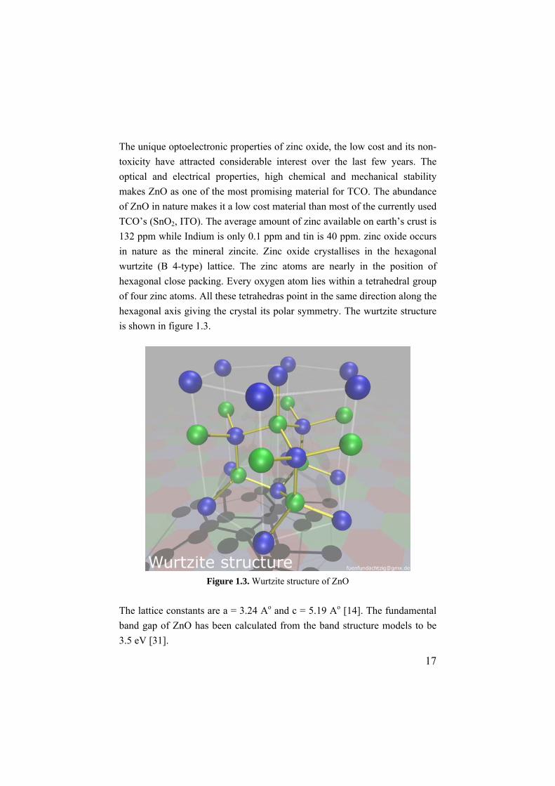
The unique optoelectronic properties of zinc oxide, the low cost and its non-toxicity have attracted considerable interest over the last few years. The optical and electrical properties, high chemical and mechanical stability makes ZnO as one of the most promising material for TCO. The abundance of ZnO in nature makes it a low cost material than most of the currently used TCO’s (SnO2, ITO). The average amount of zinc available on earth’s crust is 132 ppm while Indium is only 0.1 ppm and tin is 40 ppm. zinc oxide occurs in nature as the mineral zincite. Zinc oxide crystallises in the hexagonal wurtzite (B 4-type) lattice. The zinc atoms are nearly in the position of hexagonal close packing. Every oxygen atom lies within a tetrahedral group of four zinc atoms. All these tetrahedras point in the same direction along the hexagonal axis giving the crystal its polar symmetry. The wurtzite structure is shown in figure 1.3.
Figure 1.3. Wurtzite structure of ZnO
The lattice constants are a = 3.24 Ao and c = 5.19 Ao [14]. The fundamental band gap of ZnO has been calculated from the band structure models to be 3.5 eV [31].
18
Zinc oxide has attracted the interest of researchers due to its various properties over the years, as a TCO much research has been carried out and more recently the reports of p type doping in ZnO has ensured that this material remains in the focus of frontiers of material research for some more time. The stability of ZnO has prompted it to be used in space applications. Tonon et al have irradiated ZnO pigments coated on aluminium substrates with electrons and protons and studied the degradation of ZnO. The studies conclude that the damage rate is low for ZnO [32]. Thin films of ZnO are suitable as electrode material for optoelectronic devices. ZnO has been grown on InP and Si substrates with more than 80% transmission and resistivity as low as 3 X 10⁻⁴ Ω cm [33]. Acoustoelectric devices such as surface acoustic wave devices (SAW) have been fabricated with ZnO. For example a 1.5 G Hz. SAW filter with a minimum loss of 1.3 dB and a stopband attenuation of more than 30 dB in the frequency range below that of passband which can be used in mobile communication terminals has been fabricated [34]. Due to the unique conducting mechanism based on oxygen vacancies, ZnO has been used to fabricate oxygen gas sensors. ZnO also exhibit good piezoelectric properties. ZnO and ZnO:Al thin films have been deposited by rf planar magnetron sputtering. The piezoelectric properties of ZnO enable the fabrication of gas sensors in the SAW structure. ZnO:Al thin films have better sensitivity towards O2 [35]. Diluted magnetic semiconductors in which magnetic ions substitute for cations of the host semiconductor material are assumed to be ideal systems for spintronics. 3d transition metal doped ZnO have shown ferromagnetic behaviour above room temperature [36]. The varistors prepared by mixing zinc oxide with oxides of various metals finds application as surge controllers in electronic industry [37]. ZnO shows very strong spontaneous and stimulated emissions by excitons even at room temperature. This implies that the ZnO can be used for fabricating light emitting diodes(LED) and Laser diodes (LD). Theraja et al have demonstrated random lasing action in optically pumped ZnO powder
19
sample. The lasing action is attributed to multiple scattering in the powder [38]. Bagnall et al report the laser emission from exciton – exciton scattering at intermediate intensities and electron - hole plasma emission at higher intensities for MBE grown ZnO epilayers with a threshold intensity of 240 kW cm-1 [39]. The non linear optical response of ZnO thin films prepared by pulsed laser deposition (PLD) for various thickness and crystallinity show that the second order susceptibility to be as large as 10 pm/V. These non linear effects originate at the grain boundaries and interfaces. [40] Doping of ZnO films with Al, Ga, In, Ge, improves their electrical conductivity. [41] Aluminium doped zinc oxide films show high transmittance from UV to near IR region and nearly metallic electrical conductivity. They are used as the transparent electrodes in solar cells. Al doped ZnO films have been widely studied and have low resistivity of 2 – 5 x 10⁻⁴ Ω cm, which is comparable to that of ITO films. Various methods of thin film preparation have been used for the growth of ZnO; like evaporation [42], Chemical vapour deposition (CVD) [43], spray pyrolysis [44], magnetron sputtering [45] and pulsed laser deposition (PLD) [46]. For growing high quality ZnO films PLD has attracted much attention since PLD enables the growth of high quality thin film at relatively low substrate temperature. Ohya et. al [47] have used dip coating to deposit ZnO thin films. The films were initially fired at various temperatures ranging from 400 oC to 700 oC for 30 minutes or 1 hour. The resistivities of such films were very high. The films were later annealed at 500 oC to 700 oC in N2 atmosphere for 30 minutes this reduced the resistivity by two orders of magnitude. As the aluminium content is increased the resistivity increases while as the indium content increases, the resistivity decreases. ZnO thin films deposited by spray pyrolysis at a substrate temperature of 500 oC and the effect of Al and In doping has been studied. The effects of annealing in vacuum and argon atmosphere at 300 oC were also studied and indium is reported to be a better dopant than Al for ZnO [48].
20
Effect of N doping on the properties of ZnO films has been studied by Y. Sato et. al. [49] Zinc was evaporated in mixture of oxygen and nitrogen atmosphere. N2/ N2+ O2 varied from 0 % to 100%. 80 W RF discharge was used to excite the gasses in order to increase their reactivity. Resistivity increases from 0.1 Ω cm to 10 Ω cm as more N is incorporated into the films. Reactive evaporation with dc glow discharge in a controlled O2 atmosphere was used to grow ZnO films of resistivity 1.4 X 10⁻³ Ω cm and transmission greater than 90% [50]. The study of growth processes of ZnO thin films by PLD indicates polycrystalline growth for thin films as thin as 10 nm and oriented growth from about 50 nm. Initial growth is an amorphous layer of ZnO on glass, since the energy of formation of glass ZnO interface is very large, no crystalline phase occurs. The growth of ZnO further on the amorphous layer of ZnO requires less energy for crystallizing hence polycrystalline ZnO begins to grow from about 10 nm. After 50 nm thickness oriented ZnO grows upon the polycrystalline ZnO [51]. The films grown even in the presence of O2 background pressure were oxygen deficient. Though the films grown in vacuum (ZnO0.75) were more deficient than those grown in presence of 5 mtorr (ZnO0.95 ) O2 gas, none of the films were stoichiometric [52]. The PL emission spectrum of ZnO has been extensively studied. The large excitonic binding energy of ZnO, almost 60 MeV, make it a promising candidate as UV emitter. The PL emission at 385 nm is due to the band gap emission. The PL spectrum of ZnO obtained by exciting with 270 nm shows emissions at 380 nm and 520 nm. PL spectra obtained after the samples were irradiated with electrons and protons showed a quenching of the 520 nm line. The fact that the 520 nm line is more quickly quenched in both cases even though the total dose of the electron irradiation was less suggests that the nature of defects involved in optical degradiation is the same with electrons and protons. The 380 nm line is attributed to the band gap emission of the material while the 520 nm line is attributed to the emission due to structural
21
disorder. This could be either due to oxygen vacancies or interstitial zinc ions [53]. The luminescent centres should be related to one of the three charge states whose existence has been proved for vacancy.
1. The F centre which is a neutral vacancy occupied by two electrons, acting as a shallow donor at about 0.05 eV from the valance band.
2. The F+ centre, which is a positively charged centre and forms a trap at about 0.3 eV below the conduction band.
3. F2+ centre, a doubly ionised centre at 0.8 eV – 2.0 eV below the conduction band.
The PL intensities of 540 nm for the ZnO films depend more on the stoichiometry of the films than on the textured grain size of the polycrystalline films [54]. The 540 nm emission is attributed to the oxygen vacancies [55]. 11..55 pp-- TTyyppee TTrraannssppaarreenntt CCoonndduuccttoorrss NiO thin film was the first reported p-TCO with a moderate 40% transparency in the visible region and a high 7.0 S cm1 room-temperature conductivity [56]. The bandgap of NiO single crystal is between 3.6 and 4.0 eV.[57]. Nickel vacancies as well as excess oxygen in interstitial sites are responsible for enhanced p-type conductivity of the material.[58] The p type TCOs reported so far generally have less conductivity than that reported for n type TCOs. The large electronegativity of oxygen could be producing a strong localisation of the valance band edge of oxides thereby producing a deep trap where positive holes are localised [59]. These holes cannot migrate even under an applied field. Thus efforts should be made to modulate or modify the energy band structure to reduce the localisation of the valance band edge so as to increase the mobility of the holes. Cu2O and Ag2O show p type conductivity. However their low band gap (~ 2eV) make it impossible to use them as transparent conductors. Analysing the structure of these compounds show linear coordination of two oxygen ions to Cu+ ions
22
this could be an indication of the fact that the 3d10electrons of Cu+ have comparable energy with O 2p6 electrons. This could be reducing the localization effects of the traps produced at the valance band edge. But the three dimensional interaction of Cu+ ions should be expanding the band edge effectively reducing the band gap. Thus if the Cu+ interactions could be reduced while the linear coordination with two oxygen atoms be retained in any crystal structure, this would produce p type transparent conductors. Owing to the strong ionic nature of metal-oxygen bonding, holes are typically localized at the valence band edge, which is dominated by oxygen-2p levels therefore limiting p-type conduction. Two methods have been suggested to enhance the covalency between metal oxygen bonding, thereby limiting localization. Choosing cations having closed d-shells of energy comparable to that of the oxygen-2p levels (i.e., Cu+, Ag+, and Au+, especially when found in linear coordination with oxygen [60]), and choosing a structure in which oxygen adopts tetrahedral coordination. An aggressive search for a viable p-type TCO was motivated by the report of Kawazoe et al. on the optical and electrical properties of copper aluminate (CuAlO2) thin films prepared by laser ablation. CuAlO2, which crystallizes in the delafossite structure having the general formula A1+B3+O2- show p-type conduction. The delafossite structure comprises of alternating layers of slightly distorted edge-shared BO6 octahedral and two-dimensional close-packed A-cation planes forming linear O–A1+–O “dumbbells” [61] as found in the well-known p-type oxide semiconductor Cu2O[62]. The delafossite structure is shown in figure 1.4. Furthermore, the oxygen atoms are coordinated by four cations (one A+1 and three B3+). Depending on the stacking of the layers, two polytypes are possible.
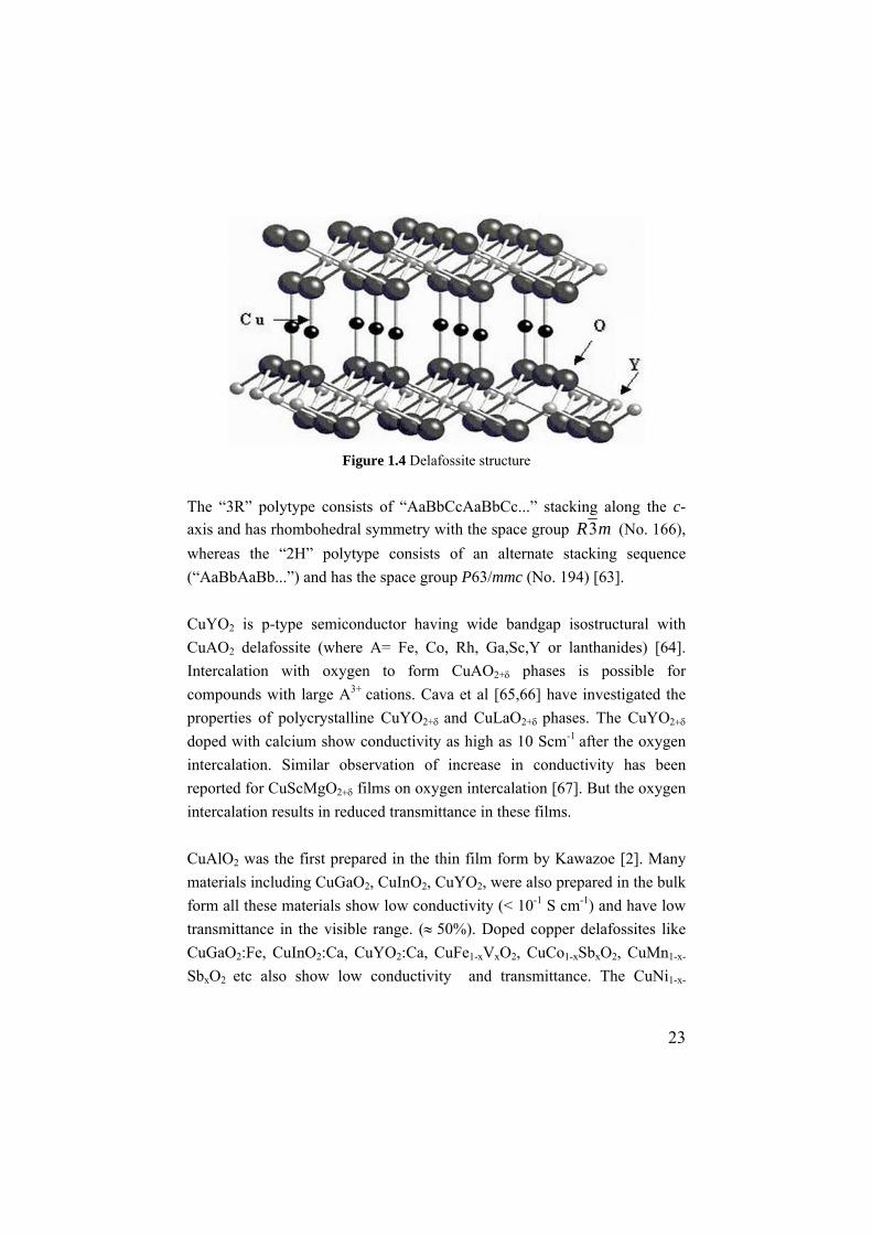
23
Figure 1.4 Delafossite structure
The “3R” polytype consists of “AaBbCcAaBbCc...” stacking along the c-axis and has rhombohedral symmetry with the space group mR3 (No. 166), whereas the “2H” polytype consists of an alternate stacking sequence (“AaBbAaBb...”) and has the space group P63/mmc (No. 194) [63]. CuYO2 is p-type semiconductor having wide bandgap isostructural with CuAO2 delafossite (where A= Fe, Co, Rh, Ga,Sc,Y or lanthanides) [64]. Intercalation with oxygen to form CuAO2+δ phases is possible for compounds with large A3+ cations. Cava et al [65,66] have investigated the properties of polycrystalline CuYO2+δ and CuLaO2+δ phases. The CuYO2+δ doped with calcium show conductivity as high as 10 Scm-1 after the oxygen intercalation. Similar observation of increase in conductivity has been reported for CuScMgO2+δ films on oxygen intercalation [67]. But the oxygen intercalation results in reduced transmittance in these films. CuAlO2 was the first prepared in the thin film form by Kawazoe [2]. Many materials including CuGaO2, CuInO2, CuYO2, were also prepared in the bulk form all these materials show low conductivity (< 10-1 S cm-1) and have low transmittance in the visible range. (≈ 50%). Doped copper delafossites like CuGaO2:Fe, CuInO2:Ca, CuYO2:Ca, CuFe1-xVxO2, CuCo1-xSbxO2, CuMn1-x-
SbxO2 etc also show low conductivity and transmittance. The CuNi1-x-

24
SbxO2:Sn delafossite thin films with were obtained reasonable conductivity of 5 x 10⁻² S cm-1 and transmittance of 60% in the visible range [68] Silver based delafossites are difficult to synthesis by solid state reactions. They are not as stable as the Cu based delafossites. Thin films of AgInO2 showed n type conductivity. Magnesium doping in bulk AgInO2 leads to p type conduction. Very low conductivity is observed for these powders. The other silver based delafossites reported are also low conducting. They include AgCrO2, AgScO2, and AgGaO2. p type conductivity of 2 x 10⁻¹ S cm-1 and transparency of 50% in the visible is obtained for thin films of AgCoO2 [68]. The cause of p type conductivity in these materials is due to excess oxygen (or metal deficit) in the crystallite sites. Changing the preparation conditions of the materials result in deviation of composition from stoichiometry in these materials. Thin film preparation of silver based delafossite compounds is a challenging task due to the instability of the silver compounds. The Cu – 3d character of the valance band edge of the copper based delafossite have an edge over the O – 2p character of the valance band edge of silver based delafossites. Since the d mainfold holes are more mobile than the p mainfold holes [69]. The origin of p type conductivity in zinc oxide has been controversial. From a first principles calculation, Yamamoto and Yoshida [70] proposed that ‘‘co-doping’’ of donor acceptor dopants (e.g. Ga and N, respectively) in ZnO might lead to p-type conduction. In this method the simultaneous doping of both acceptor (N) and donor (Ga) into the ZnO lattice were carried out with an acceptor concentration twice that of the donor concentration to get a maximum conductivity in p-ZnO. The essential approach of this method is to stabilize the N substitution in the appropriate ZnO lattice sites by the formation of N–Ga–N type bonds, which reduce the N–N repulsive interaction (Madelung Energy) thereby making the acceptor level shallower, thus enhancing the acceptor doping. Successful p type doping of ZnO was first demonstrated by Joseph et al. [71] with a room temperature resistivity
25
of 0.5 Ω cm and a carrier concentration of 5 x 1019 cm3 in p-type ZnO thin films deposited on glass substrate with Ga and N as dopants. Thin films grown by spray pyrolysis of nitrogen doped p type ZnO have a carrier concentration of 1018 cm3 and resistivity of 10-2 Ω cm [72]. The low density of compensative native defects as well as the hydrogen passivation in the ZnO:N film grown by ultrasonic spray pyrolysis (USP) probably account for the good p type conduction. The high hole mobility may be due to the nanocrystal structure of ZnO based films grown by ultrasonic spray pyrolysis. The photoluminescence spectrum exhibits a strong near-band-edge emission and a very weak deep-level emission in both undoped and N-doped ZnO films, indicating that the ZnO-based films grown by the USP technique are very close to stoichiometry and of optically high quality. p-type conductivity of intrinsic ZnO thin films deposited by plasma-assisted metal-organic chemical vapor deposition with a hole concentration above 1017 cm−3 was achieved at the growth temperatures of 250 and 300 °C. It is speculated that the oxygen chemical potential is enhanced by virtue of oxygen plasma, which can lower the formation energy of some acceptor defect, such as zinc vacancy, and this accounts for the p-type conductivity. Increasing the growth temperature to 350 and 400 °C results in n-type conductivity with an electron concentration around 1017 cm−3. The inversion to n-type conductivity can be explained as the compensation effect by the ionized oxygen vacancy donor, which is readily formed at a high growth temperatures. The p-type behavior is temperature dependent. The origin of intrinsic p-type behavior has been ascribed to the formation of zinc vacancy and some complex acceptor center. Understanding of these intrinsic acceptor states will help elucidate the extrinsic as well as intrinsic p-type doping mechanism in ZnO [73]. The films grown at optimum conditions show a resistivity of 12.7 Ω cm and a hole concentration of 1.88 x 1017 cm−3. Arsenic doped ZnO thin flms show p type conductivity. ZnO: As films grown on O – face of ZnO substrates and Si – face of SiC show p type conductivity with a carrier concentrationof 9 x 1016 cm-3 and mobility of 6 cm2/Vs. is obtained with resistivity of 12 Ω cm for thin films. The PL emission at 3.359 eV is attributed to acceptor bound exciton emission and the PL emission at 3.322 eV and 3.273 eV is attributed to recombination
26
emissions between free electrons and acceptor holes. The donor to acceptor recombinations result in PL emissions at 3.219 eV and 3.172 eV. [74]. p-type conduction in ZnO thin films has also been realized by Al–N co-doping method. ZnO:Al,N thin films were prepared in NH3–O2 atmosphere with the substrate temperature in the range of 360–600 OC. The conduction type of Al–N co-doped ZnO thin films are dependant greatly on the growth temperature. Room temperature resistivity of 24.5 Ω cm and a hole concentration of 7.48 x 1017 cm3 with a Hall mobility of 0.341 cm2 / V s in ZnO thin films on sapphire substrate. The substrate temperature exerts a remarkable influence on the structural characteristics this is because that the substrate temperature restricts diffusion behaviour of nucleation particle on substrate surface. According to the nucleation theory, for a perfect heteroepitaxy nucleation, it is necessary to satisfy surface diffusion condition, the substrate temperature must be higher than a critical value. Below this value, the sputtering molecules or atoms with higher energy can also be ‘‘cooled’’ quickly, their surface diffusion length is greatly reduced, and they cannot migrate to nucleation position. The surface of the film obtained under the critical temperature would be rough and with polycrystal or amorphous structure. When the growth temperature is too high, the absorption life of ZnO molecule will be shortened, and the decomposition of ZnO molecule is faster than the combination of Zn and O, even under high partial pressure of O2. This will introduce local Zn-rich region and result in a large number of point defect (Vo or Zno), even leading to amorphous state in the ZnO film [75]. The development of p type transparent oxide materials has lead to the fabrication of all oxide diodes and transistors. The progress achieved in the field of semiconductor oxide diodes and transistors has paved way for newer applications for transparent conductors and a new field of electronics called Transparent Electronics has been defined. The realization of a transistor is of great importance in the context of transparent electronics since the control electrode of such a device facilitates the achievement of logic, amplification, memory, and other types of signal conditioning and processing functions which, within the context of microelectronics, play an important role in our modern information society.
27
The conventional thin film transistors developed with opaque elements or polymers have a drawback that their control electrodes are opaque. Thus from the point of view of transparent electronics, one challenge facing polymer light emitting devices centres around the thin-film transistor (TFT) array control circuitry. While needed for maximized brightness and efficiency, the opaque TFTs restrict the amount of light that can be transmitted to the observer. OLEDs and PLEDs lack the intrinsic property of bistable emission, therefore they must be driven by higher voltages and currents for suitable brightness in a passive matrix addressing scheme. The light emitting pixels may be controlled by a thin-film transistor array for much better brightness and efficiency. Unfortunately, the current opaque TFTs severely restrict the amount of light detected by the observer. Depending upon the design of the array and interconnects, typically only a fraction of the emitted light is used by the observer for the information. A large portion of the energy of the display is lost. One method to increase the efficiency is to combine the recent progress in transparent oxides that are semiconducting to near-metallic with the PLEDs. ZnO is one of a few oxides that can be grown as a crystalline material at relatively low deposition temperatures on various substrates such as amorphous glasses and plastics. By using these characteristics it is possible to realize thin film transistors by using ZnO as the active channel layer. It is expected that the characteristics of ZnO–TFT’s will not degrade on exposure to visible light, due to the wide band gap of its active channel layer, whereas the characteristics of amorphous Si TFTs and poly-Si TFTs do degrade. Therefore, there is no need to shield the active channel layer from visible light in TFT’s when ZnO is used as the active channel. This makes the TFT structurally simple and transparent to visible light, which would allow the aperture ratio of active matrix arrays to be increased. [76] ZnO is a material with excellent properties for developing transparent electronic devices.

28
11..66 CCoonncclluussiioonn In general, the traditional groups of materials used to build transparent conducting oxides include SnO2, In2O3, ZnO (doped with F or Al), and CdO. However indium oxides are volatile, cadmium is poisonous. Several binary oxides are unstable, CdO converts to Cd(OH)2, In2O3 converts to In(OH)3 at less than 150oC, SnO2 absorbs water. Only zinc oxide can be doped to form either p type or n type material. The p type TCO’s of delafossite structure are generally less transparent (hardly 50% at 500nm) than ZnO. Thus useful devices can be fabricated only using ZnO thin films that show better than 80% transmittance over the entire visible spectrum. It would be sensible to work towards understanding the basic growth mechanisms and reasons for p type conduction in ZnO or for the methods to increase transmittance in delafossite structure materials. Thus on the point of the consideration of cost, toxicity or environmental considerations and applications zinc oxide far surpasses competition from any other material under current research interest.
29
11..77 RReeffeerreenncceess [1.] K. Badeker, Ann. Phys. 22 (1907) 749 [2.] H. Kawazoe, M. Yasukawa, H. Hyodo, M. Kurita, H. Yanagi and H. Hosono, Nature 389 (1997) 939
[3.] R.L.Hoffman, B.J.Norris and J.F.Wager, Appl. Phy.Lett 82 (2003) 733
[4.] P.P. Edwards, A. Porch, M.O. Jones, D.V. Morgan and R.M. Perks, Dalton Trans. (2004) 2995
[5.] H. Ohta and H. Hosono, Materials Today 7 (2004) 42 [6.] D. J. Griffits, Introduction to Electrodynamics, Prentice – Hall of India, New Delhi, (1994)
[7.] I. Hamberg and C.G. Granqvist, J. Appl. Phys. 60 (1986) R123 [8.] J. Hu and R. G. Gordon, J Appl. Phys. 71 (1992) 880 [9.] I. Hamberg, A. Hjortsberg, and C. G. Granqvist, Appl. Phys. Lett. 40 (1982) 362
[10.] R. G. Gordon, Proc. Of MRS workshop “Transparent conducting oxides (TCOs)” August (2000) 5
[11.] K. L. Chopra, S. Major and D. K. Pandya, Thin Solid Films 102 (1983) 1
[12.] E. Shanthi, V. Dutta, A. Banerjee, and K. L. Chopra, J. Appl. Phys. 51 (1980) 6243
[13.] A .De and S. Ray, J. Phys. D: Appl.Phys. 24 (1991) 719 [14.] H.L. Hartnagel, A.L. Dawar, A.K.Jain and C. Jagadish, Semiconducting transparent thin films, IOP publishers (1995)
[15.] J. Bardeen and W. Shockley, Phys. Rev. 80 (1950) 72 [16.] A. R. Huston, J. Appl. Phys. 32 (1961) 2287 [17.] H. Ehrenreich, J. Appl. Phys. 32 (1961) 2155 [18.] C. Erginsoy, Phys. Rev. 79 (1950) 1013 [19.] V. A. Johnson, and K. Lark–Horovitz, Phys. Rev. 71 (1947) 374 [20.] J. Appel, Phys. Rev. 122 (1961) 1760 [21.] R. L Petritz, Phys. Rev. 104 (1956) 1508 [22.] T. J.Coutts, D. L. Young and L. Xiaonan, MRS Bull. 8 (2000) 58 [23.] D. B. Fraser and H. D. Cook, J. Electrochem. Soc. 119, (1972) 1368
30
[24.] G. Haacke, Appl. Phys. 47, (1976) 4086 [25.] P. A. Iles and S. I. Soclof, I. E. E. Photovoltaic Specialists Conference, (1976) 978
[26.] Ti X. Li, T. Gessert, C. DeHart, T. Barnes, H. Moutinho, Y. Yan, D. Young, M. Young, J. Perkins, and T. Coutts, NREL/CP-520- 31017 (2001)
[27.] R. L. Hoffmann, Master of Sciences Thesis, Oregon State University (1992)
[28.] B.J. Ingram, G.B. Gonzalez, D.R. Kammler, M.I. Bertoni and T.O. Mason, Journal of Electroceramics, 13, (2004) 167
[29.] P.P. Edwards, A. Porch, M. O. Jones, D. V. Morgan, and R. M. Perks, Dalton transactions B408864F (2004)
[30.] M. Chen, Z.L. Pei, X. Wang, Y. H. Yu, X.H. Liu, C. Sun and L. S. Wen, J. Phys D 33, (2000) 2538
[31.] U. Rossler, Phys. Rev. 184 (1969) 733 [32.] C. Tonon, C. Duvignacq, G. Teyssedre and Magdeleine, J.Phys. D: Appl Phys. 34 (2001) 124
[33.] M. Purica, E. Budianu and E. Rusu, Thin solid films 383 (2001) 284
[34.] J.Kioke, K. Shimoe, H. Ieki, Jpn. J.Appl.Phys. 32. (1993) 2337 [35.] M. Penza, C. Martucci, V. I. Anisimkin, and L. Vasanelli, Materials science fourm 203 (1996) 137
[36.] P. Sharma A. Gupta, K. V. Rao, F. J. Owens, R. Sharma, R. Ahuja, J. M. O. Guillen, B. Johansson and G. A. Gehring Nature mater. 2. (2003) 673.
[37.] A. Bui, H. T. Nguyen and A. Loubiere J. Phys. D: Appl Phys. 28 (1995) 774.
[38.] R. K. Theraja, A. Mitra, Appl. Phys. B 71 (2000) 181 [39.] D. M. Bagnall, Y. F. Chen, Z. Zhu, T. Yao, S. Koyama, M.Y. Shen, T. Goto, Appl. Phys. Lett. 70 (1997) 230.
[40.] H. Cao, J. Y. Wu, H. C. Ong, J. Y. Dai, and R. P. H. Chang, Appl. Phys. Lett., 73 (1998) 3
[41.] Wang R, King L H and Sleight A W J Mater. Res. 11 (1996) 1659.
31
[42.] J. H. Morgan and D. E. Brodie, Can. J. Phys. 60, (1982) 1387. [43.] J. Lu, Z. Ye, J. Huang, L. Wang, and B. Zhao, Appl. Sur. Sci. 207, (2003) 295.
[44.] P. Nunes, E. Fortunato, R. Martins, Thin Solid Films 383 (2001) 277.
[45.] K. K. Kim, H. S. Kim, D. K. Hwang, J. H. Lim, S. J. Park, Appl. Phys. Lett 83, (2003) 63.
[46.] S. J. Henley, M. N. R. Ashfold, D. Cherns, Surface and Coatings Technology 177–178, (2004) 271
[47.] Y. Ohya, H. Saiki and Y. Takahashi, J. Mater. Sci. 29 (1994) 4099
[48.] P. Nunes, B. Fernandes, E. Fortunato, P. Vilarinho, R. Martins, Thin Solid Films 337 (1999) 176
[49.] Y. Sato and S. Sato, Thin Solid Films 281–282 (1996) 445 [50.] J. H. Morgan and D.E. Brodie, Can. J. Phys. 60 (1982) 1387. [51.] S. Hayamizu, H. Tabata, H. Tanaka, and T.Kawai J. Appl. Phys. 80 (1996) 787
[52.] S. V. Prasad, S. D. Walck, J.S. Zabinski, Thin solid Films 360 (2000) 107
[53.] C. Tonon, C. Duvignacq, G. Teyssedre and Magdeleine, J.Phys. D: Appl Phys. 34 (2001) 124
[54.] S.H. Bae, S. Y. Lee, B.J. Jin, S. Im Appl. Sur. Sci. 169–170, (2001) 525
[55.] K. Vanheusden, C.H. Seager, W. L. Warren, D. R. Tallant, J. A. Voigt, Appl. Phys. Lett. 68, (1996) 403.
[56.] H.Sato, T.Minami, S.Takata, T.Yamada, Thin Solid Films 236 (1993) 27
[57.] D. Adler, J. Feinleib, Phys. Rev. B 2 (1970) 3112. [58.] E. Antolini, J. Mater. Sci. 27 (1992) 3335. [59.] Hiroshi Yanagi, Transparent p/n type oxide semiconductors with delafossite structure: Chemical design and material exploration. Thesis (2001).
[60.] H. Kawazoe, M. Yasukawa, H. Hyodo, M. Kurita, H. Yanagi and H. Hosono, Nature 389 (1997) 939
32
[61.] Hiroshi Kawazoe, Hiroshi Yanagi,Kazushige Ueda, and Hideo Hosono MRS Bulletin (2000) 28
[62.] L. Kleinman, And K. Mednick, Phys. Rev. B 21, (1980) 1549 [63.] K. Ueda, S. Inoue, H. Hosono, N. Sarukura and M. Hirano. Appl. Phys. Lett. 78 (2001) 2333.
[64.] R. D. Shannon, D. B. Rogers, and C.T. Prewitt, Inorg Chem 10 (1971) 713.
[65.] R. J. Cava, H. W. Zandbergen, A. P. Ramierz, H. Takagi, C. T. Chen, J. J. Krajewski, W. F. Peck.jr, J. V. Waszczak, G. Meigs, R. S. Roth, and L. F. Schneemeyer, J. Solid state chem. 104 (1993) 437.
[66.] R. J. Cava, W. F. Peck.jr, J. J. Krajewski, S. W. Chenog, and H. Y. Hwang, J. Mater Res 9 (1994) 314.
[67.] H. Yanagi, S. Park, A. D. Draeseke, D. A. Keszler and J.Tate, J. Solid state chem 175 (2003) 34.
[68.] J. Tate, M. K. Jayaraj, A. D. Draeseke, T. Ulbrich, A. W. Sleight, K. A. Vanaja, R. Nagarajan, J. F. Wager, R. L. Hoffman, Thin solid films, 411 (2002) 119.
[69.] A.N. Banerjee, K. K. Chattopadhyay, Progress in Crystal Growth and Characterisation of materials. 50 (2005) 52
[70.] T. Yamamoto, H.K. Yoshida, Jpn. J. Appl. Phys. 38 (1999) L166. [71.] M. Joseph, H. Tabata, T. Kawai, Jpn. J. Appl. Phys. 38 (1999) L1205.
[72.] Jun-Liang Zhao, Xiao-Min Li, Ji-Ming Bian, Wei-Dong Yu, Can- Yun Zhang, Journal of Crystal Growth 280 (2005) 495.
[73.] Y. J. Zeng, Z. Z. Ye, W. Z. Xu, J. G. Lu, H. P. He, L. P. Zhu, B. H. Zhao, Y. Che and S. B. Zhang Applied Physics Letters 88, (2006) 262103
[74.] Y.R.Ryu, T.S.Lee and H.W.White, Appl. Phys. Lett. 83 (2003) 87. [75.] Guodong Yuan, Zhizhen Ye, Qing Qian, Liping Zhu, Jingyun Huang,Binghui Zhao, Journal of Crystal Growth 273 (2005) 451
[76.] Satoshi Masuda, Ken Kitamura, Yoshihiro Okumura, Shigehiro Miyatake, Hitoshi Tabata and Tomoji Kawai, J. Appl. Phys. 93 (2003) 1624