Embed Size (px)
Citation preview

CHAPTER 1
Introduction
Contents
1.1 Motivation 21.1.1 Advantages of Millimeter-Wave Radios 21.1.2 Deep-Submicron CMOS 51.1.3 Digitally Intensive Approach 7
1.2 Design Challenges 91.2.1 Toward All-Digital PLL in mm-Wave Regime 91.2.2 Wide Tuning Range and Fine Frequency Resolution 111.2.3 Linear Wideband FM 12
References 13
Wireless communication has evolved remarkably since Guglielmo Marconi
demonstrated the transmission and reception of Morse-coded messages
across the Atlantic Ocean in the early twentieth century. Since then, new
wireless communication methods and services have been continuously
adopted that revolutionize our lives. Today, cellular, mobile, and wireless
local-area networks (WLANs), afforded by breakthroughs in semiconductor
technologies and their capability of mass production, are in use worldwide.
They enable us to share images of our cherished moments with family and
friends anywhere, and at anytime. The current trends toward
portable wireless devices with ultra-high-speed (e.g., gigabit per second)
connectivity will soon allow us to go online via our notebooks, cell
phones, and tablets, simultaneously emailing, chatting with friends, web
browsing and downloading movies and music in a fraction of the time it
takes today. These devices will have to meet aggressive performance
specifications in a sufficiently small and low-cost product at low power
dissipation. This has prompted frantic research into new radio frequency
(RF)-integrated circuits, system architectures, and design approaches.
This book explores the feasibility, advantages, design, and testing of
digitally intensive frequency synthesis in the millimeter-wave (mm-wave)
frequency range. An all-digital phase-locked loop (ADPLL)-based transmitter
1Millimeter-Wave Digitally Intensive Frequency Generation in CMOS.DOI: http://dx.doi.org/10.1016/B978-0-12-802207-8.00001-0
© 2016 Elsevier Inc.All rights reserved.

demonstrator fabricated in a production bulk CMOS process is described,
which operates in the 60-GHz band, and achieves fractional frequency
generation and wideband frequency modulation (FM). This digitally
intensive design has the potential for low cost in volume production. It
is also amenable to scaling in future technology nodes as opposed to
other analog-intensive implementations. The silicon area and power
consumption of such transmitters may be reduced further in future by
harnessing the power of digital signal processing (DSP).
1.1 MOTIVATION
To achieve gigabit per second (i.e., Gb/s) transfer rates, Wi-Fi technology
(IEEE 802.11ac in the 5-GHz band) [1] has been developed in recent
years. Multistation WLAN throughput of at least 1 Gb/s, and a single link
throughput of at least 500 Mb/s is specified. It employs RF bandwidths of
up to 160 MHz, multiple-input and multiple-output (MIMO) array
transmitter/receiver streams (up to 8), multi-user MIMO, and up to
256-QAM (quadrature amplitude modulation) schemes in order to achieve
that level of performance. The mm-wave frequency bands, by contrast, are
less crowded than the low-gigahertz radio communication bands and, more
attractively, have wider license-free RF bandwidth available (e.g., 7 GHz
bandwidth in the 60-GHz band). This will enable the gigabit-per-second
short-range communication for consumer multimedia products and support
the development of emerging short-range wireless networking in many
important areas, for example, commerce, manufacturing, transport, etc.,
and thus provide significant growth potential in new internet applications
in price-sensitive communication markets.
In the following sections, the advantages and challenges of mm-wave
transceiver design in CMOS technology will be examined. The focus is
on mm-wave frequency synthesis.
1.1.1 Advantages of Millimeter-Wave RadiosThe mm-wave frequency band is defined as 30�300 GHz with a wave-
length between 1 and 10 mm in the air [2]. There are various aspects of
mm-wave bands that make it attractive for short-range applications. One
major advantage is the bandwidth available to carry information. To keep
operating costs low, regulatory licensed bands should be avoided, thus
calling for the exploitation of the unlicensed or the industrial, scientific,
and medical (ISM) radio bands. Figure 1.1 plots the available bandwidth
2 Millimeter-Wave Digitally Intensive Frequency Generation in CMOS
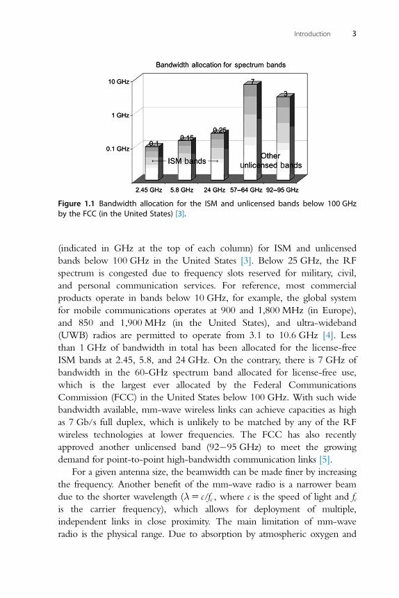
(indicated in GHz at the top of each column) for ISM and unlicensed
bands below 100 GHz in the United States [3]. Below 25 GHz, the RF
spectrum is congested due to frequency slots reserved for military, civil,
and personal communication services. For reference, most commercial
products operate in bands below 10 GHz, for example, the global system
for mobile communications operates at 900 and 1,800 MHz (in Europe),
and 850 and 1,900 MHz (in the United States), and ultra-wideband
(UWB) radios are permitted to operate from 3.1 to 10.6 GHz [4]. Less
than 1 GHz of bandwidth in total has been allocated for the license-free
ISM bands at 2.45, 5.8, and 24 GHz. On the contrary, there is 7 GHz of
bandwidth in the 60-GHz spectrum band allocated for license-free use,
which is the largest ever allocated by the Federal Communications
Commission (FCC) in the United States below 100 GHz. With such wide
bandwidth available, mm-wave wireless links can achieve capacities as high
as 7 Gb/s full duplex, which is unlikely to be matched by any of the RF
wireless technologies at lower frequencies. The FCC has also recently
approved another unlicensed band (92�95 GHz) to meet the growing
demand for point-to-point high-bandwidth communication links [5].
For a given antenna size, the beamwidth can be made finer by increasing
the frequency. Another benefit of the mm-wave radio is a narrower beam
due to the shorter wavelength (λ5 c/fc , where c is the speed of light and fcis the carrier frequency), which allows for deployment of multiple,
independent links in close proximity. The main limitation of mm-wave
radio is the physical range. Due to absorption by atmospheric oxygen and
Figure 1.1 Bandwidth allocation for the ISM and unlicensed bands below 100 GHzby the FCC (in the United States) [3].
3Introduction

water vapor, signal strength drops off rapidly with distance compared to
other bands. Figure 1.2 illustrates the general trend of increasing the
attenuation of radio waves with frequency (due only to atmospheric losses;
free space path loss is not accounted for) [6]. Atmospheric absorption by
oxygen causes more than 15 dB/km of attenuation. The loss of a link
budget at 60 GHz is therefore unacceptable for long-distance communica-
tion (e.g., .1 km), but can be used to an advantage in short-range indoor
communications because the limited range and narrow beamwidths prevent
interference between neighboring links. These attributes have led to greatly
reduced regulatory burdens for mm-wave communications.
Due to its potential for short-range, gigabit-per-second communications,
several standards in the 60-GHz band have been established in recent
years. The IEEE 802.15.3c standard was approved in 2009 for wireless
personal-area network [7]. A similar standard for Europe (ECMA-387 [8])
was published in 2008. The WirelessHD consortium has released a specifica-
tion version 1.0a for regulating the transmission of high-definition video in
this unlicensed band [9]. Most recently, the IEEE 802.11ad standard (known
as WiGig) [10] was adopted in 2013. It provides data rates up to 7 Gb/s, or
more than 103 the maximum speed previously supported by the IEEE
802.11 standard. IEEE 802.11ad also adds a “fast session transfer” feature,
Figure 1.2 Average atmospheric attenuation of radio waves propagating throughfree space versus frequency [6].
4 Millimeter-Wave Digitally Intensive Frequency Generation in CMOS
which enables wireless devices to seamlessly transition between the 60-GHz
frequency band and legacy bands at 2.4 and 5 GHz in order to optimize link
performance and range criteria.
In addition to the gigabit-per-second communication, the 60-GHz
unlicensed band also holds promise for integrating wireless sensors.
Frequency-modulated continuous-wave (FMCW) radars may be utilized
for presence detection and ranging at 60-GHz applications, where
high-frequency resolution is required [11]. This is also the intended
application for the realized ADPLL frequency synthesizer that is fully
described in this book. As an example of such FMCW application is a
gesture recognition system for cars, where the driver gestures (e.g.,
nodding the head) without taking the eyes off the road when interfacing
with applications such as navigation, phone, HVAC (heating, ventilating,
and air conditioning) controls, etc. The targeted detection range is
from 0.3 to 10 m and the range resolution is below 5 cm. A low-cost
implementation of short-range radar systems will enable numerous
applications in security, search and rescue, imaging, logistics, quality
control, to name just a few.
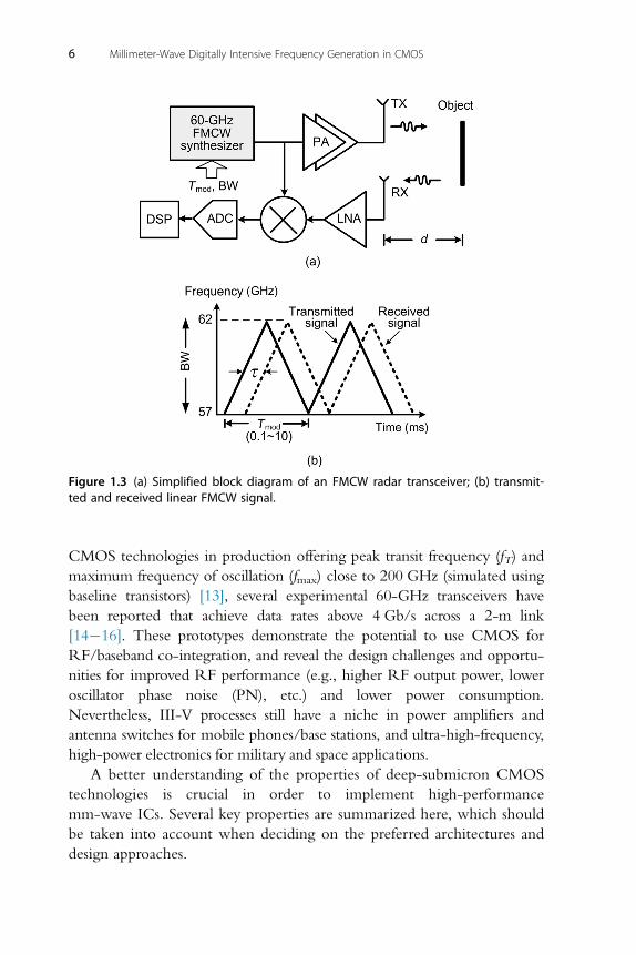
Figure 1.3 illustrates the operating principle of an FMCW radar
transceiver. The carrier signal is modulated as shown in Figure 1.3b,
resulting in a signal whose instantaneous frequency varies linearly with
time, i.e., a linear chirp [12]. This linear chirp is transmitted toward a
target, and the received echo is convolved with a portion of the transmit-
ted signal to determine the round-trip propagation time, τ. In an FMCW
radar, the achievable range resolution (Δr) is determined by
Δr5c
2UBW0 (1.1)
where c is the speed of light, and BW (Figure 1.3b) is the modulation
range of the transmit signal [12]. When the full 7 GHz of bandwidth at
60 GHz is utilized, a range resolution as fine as 2 cm can be achieved.
1.1.2 Deep-Submicron CMOSSilicon technologies (e.g., CMOS and SiGe-BiCMOS) are mainstream inte-
grated circuit (IC) processes driven largely by mass production of ICs used in
digital computers (e.g., desktops and notebooks) and other electronic devices
(e.g., cell phones, game consoles, and tablets). The demand for a higher inte-
gration level and lower cost in volume production has driven mm-wave
electronics development in silicon CMOS technology. With 65-nm bulk
5Introduction
CMOS technologies in production offering peak transit frequency (fT) and
maximum frequency of oscillation (fmax) close to 200 GHz (simulated using
baseline transistors) [13], several experimental 60-GHz transceivers have
been reported that achieve data rates above 4 Gb/s across a 2-m link
[14�16]. These prototypes demonstrate the potential to use CMOS for
RF/baseband co-integration, and reveal the design challenges and opportu-
nities for improved RF performance (e.g., higher RF output power, lower
oscillator phase noise (PN), etc.) and lower power consumption.
Nevertheless, III-V processes still have a niche in power amplifiers and
antenna switches for mobile phones/base stations, and ultra-high-frequency,
high-power electronics for military and space applications.
A better understanding of the properties of deep-submicron CMOS
technologies is crucial in order to implement high-performance
mm-wave ICs. Several key properties are summarized here, which should
be taken into account when deciding on the preferred architectures and
design approaches.
Figure 1.3 (a) Simplified block diagram of an FMCW radar transceiver; (b) transmit-ted and received linear FMCW signal.
6 Millimeter-Wave Digitally Intensive Frequency Generation in CMOS
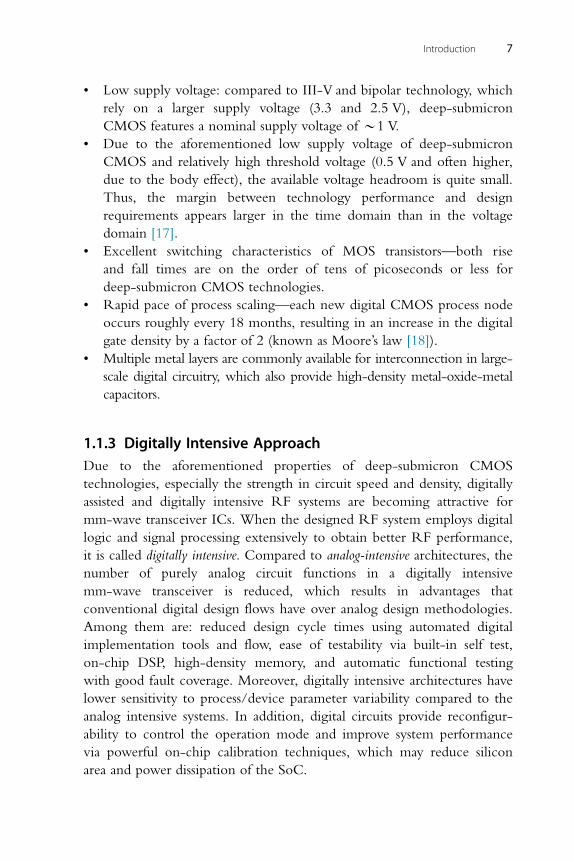
• Low supply voltage: compared to III-V and bipolar technology, which
rely on a larger supply voltage (3.3 and 2.5 V), deep-submicron
CMOS features a nominal supply voltage of B1 V.
• Due to the aforementioned low supply voltage of deep-submicron
CMOS and relatively high threshold voltage (0.5 V and often higher,
due to the body effect), the available voltage headroom is quite small.
Thus, the margin between technology performance and design
requirements appears larger in the time domain than in the voltage
domain [17].
• Excellent switching characteristics of MOS transistors—both rise
and fall times are on the order of tens of picoseconds or less for
deep-submicron CMOS technologies.
• Rapid pace of process scaling—each new digital CMOS process node
occurs roughly every 18 months, resulting in an increase in the digital
gate density by a factor of 2 (known as Moore’s law [18]).
• Multiple metal layers are commonly available for interconnection in large-
scale digital circuitry, which also provide high-density metal-oxide-metal
capacitors.
1.1.3 Digitally Intensive ApproachDue to the aforementioned properties of deep-submicron CMOS
technologies, especially the strength in circuit speed and density, digitally
assisted and digitally intensive RF systems are becoming attractive for
mm-wave transceiver ICs. When the designed RF system employs digital
logic and signal processing extensively to obtain better RF performance,
it is called digitally intensive. Compared to analog-intensive architectures, the
number of purely analog circuit functions in a digitally intensive
mm-wave transceiver is reduced, which results in advantages that
conventional digital design flows have over analog design methodologies.
Among them are: reduced design cycle times using automated digital
implementation tools and flow, ease of testability via built-in self test,
on-chip DSP, high-density memory, and automatic functional testing
with good fault coverage. Moreover, digitally intensive architectures have
lower sensitivity to process/device parameter variability compared to the
analog intensive systems. In addition, digital circuits provide reconfigur-
ability to control the operation mode and improve system performance
via powerful on-chip calibration techniques, which may reduce silicon
area and power dissipation of the SoC.
7Introduction
Note that the “digitally intensive” term doesn’t imply that analog/RF
design techniques are not important. On the contrary, they are as crucial
as before. The overall system performance is usually dominated by a few
key analog circuit blocks. The essence of the digitally intensive approach
is to make the inputs/outputs (IOs) of the RF/analog building blocks
digital so that the system can be modeled and analyzed using the digital
design flow, with its many advantages for design throughput and yield.
Consequently, it requires RF/analog designers to be conversant with
digital circuits and system design, to analyze the system from both analog
and digital perspectives, and to collaborate with digital designers.
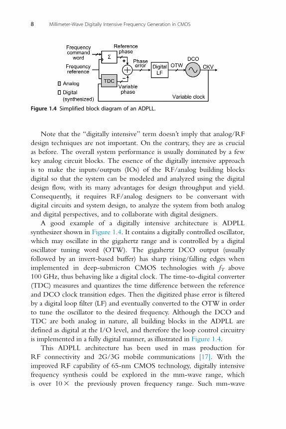
A good example of a digitally intensive architecture is ADPLL
synthesizer shown in Figure 1.4. It contains a digitally controlled oscillator,
which may oscillate in the gigahertz range and is controlled by a digital
oscillator tuning word (OTW). The gigahertz DCO output (usually
followed by an invert-based buffer) has sharp rising/falling edges when
implemented in deep-submicron CMOS technologies with fT above
100 GHz, thus behaving like a digital clock. The time-to-digital converter
(TDC) measures and quantizes the time difference between the reference
and DCO clock transition edges. Then the digitized phase error is filtered
by a digital loop filter (LF) and eventually converted to the OTW in order
to tune the oscillator to the desired frequency. Although the DCO and
TDC are both analog in nature, all building blocks in the ADPLL are
defined as digital at the I/O level, and therefore the loop control circuitry
is implemented in a fully digital manner, as illustrated in Figure 1.4.
This ADPLL architecture has been used in mass production for
RF connectivity and 2G/3G mobile communications [17]. With the
improved RF capability of 65-nm CMOS technology, digitally intensive
frequency synthesis could be explored in the mm-wave range, which
is over 103 the previously proven frequency range. Such mm-wave
Figure 1.4 Simplified block diagram of an ADPLL.
8 Millimeter-Wave Digitally Intensive Frequency Generation in CMOS

ADPLL increases the reconfigurability of frequency generation in a
mm-wave transceiver. Moreover, FM can be incorporated there to form a
digital transmitter with the potential for superior modulation quality and
lower cost in mass production.
1.2 DESIGN CHALLENGES
To realize low-cost, yet high-performance mm-wave transceivers in CMOS
technology, new concepts in IC implementations for ultra-wideband signal
generation and mm-wave front-ends are necessary. This book focuses on
frequency synthesis, which is critical to many modern communication
systems. Due to the high operating frequency, fine frequency resolution, and
wideband linear FM requirements, a fully integrated mm-wave frequency
synthesizer has various design challenges that are discussed in the following
sections.
1.2.1 Toward All-Digital PLL in mm-Wave RegimeBefore this very 60-GHz all-digital phase-locked loop (PLL) that will be
elaborated in this book, there had been no other reported successful
fractional-N synthesizer implementations above 10 GHz for wireless
applications that would employ an all-digital approach. There were,
however, two reports of digital PLL synthesizers [19,20] operating at 20
and 40 GHz, respectively, used for high-speed serial wireline applications,
and numerous successful ADPLL demonstrators operating below 10 GHz
for various wireless applications, for example, bluetooth, cellular, WLAN,
WiMAX, etc. [21�24]. For low-gigahertz applications, an LC oscillator
is normally used to satisfy stringent PN requirements, in which the
tuning of the oscillation frequency is achieved via digital control of an
array of MOS varactors that operate in flat regions of their C�V curve. It
is well-known that the PN of an LC oscillator in the upconverted
thermal noise or 1/f 2 regime (i.e., outside the loop bandwidth of a PLL
synthesizer) is inversely proportional to the square of the tank quality
factor Q [25]. The tank Q-factor below 10 GHz is dominated by the
Q-factor of the inductor, while the varactor Q-factor is normally much
higher (e.g., B100 at 2 GHz) in a 65-nm CMOS technology.
However, this is opposite to the situation at mm-wave frequencies.
Figure 1.5 plots the Q-factor and capacitance (Cv) versus bias voltage for
n1 /n-well and p1 /p-well accumulation mode varactors in a 65-nm
CMOS technology at minimum gate length [26]. Q-factor varies with
9Introduction

bias (due to changing Cv) and is approximately 20 or 5 in the flat regions.
While the inductor Q-factor (QL) increases with increasing frequency,
the Q-factor of capacitors and varactors (QC) is inversely proportional to
frequency. Therefore, Q of the tank capacitance (varactor plus parasitics)
becomes the primary factor limiting the quality of tunable on-chip
resonators, and the PN performance of mm-wave oscillators. Power
consumption of the oscillator must therefore be increased in order to
maintain signal swing and compensate for greater losses in the LC tank.
In addition, a frequency divider chain is necessary to bring the carrier
frequency down to a few GHz for further processing by the digital phase
detector. There are strong trade-offs between power, chip area (inductors),
maximum operating frequency, and operating range in the divider chain
design, which normally dissipates more than 50% of the total power in a
mm-wave analog PLL [27]. Moreover, the divider’s operating range should
be aligned with the DCO frequency tuning range in the presence of
process, voltage, and temperature (PVT) variations. The divider chain
introduces extra delay in the loop and may affect the stability of the PLL.
All these bring extra challenges to the design of mm-wave ADPLLs.
Although the digitally intensive nature of the ADPLL permits the fast
system-level simulation and verification by an event-driven simulator, the
transistor sizing and physical layout of the key “analog-nature” building
blocks, such as DCO, divider chain, and TDC have to be “handcrafted”
according to the design specifications, and then modeled at the behavioral
level for the closed-loop simulations. Compared to design for low-GHz
Figure 1.5 Capacitance and Q-factor at 60 GHz versus gate voltage for minimumlength, thin-oxide accumulation mode varactors (65-nm CMOS) [26].
10 Millimeter-Wave Digitally Intensive Frequency Generation in CMOS

applications, the interconnections between mm-wave frequency building
blocks affects the system performance due to parasitic capacitance, losses,
and unwanted capacitive and magnetic coupling effects. Therefore, inten-
sive electromagnetic simulation is also required for a successful ADPLL
design in the mm-wave regime.
1.2.2 Wide Tuning Range and Fine Frequency ResolutionAs mentioned earlier, one major benefit of the 60-GHz band is the 7-GHz
worth of unlicensed bandwidth. When the 7-GHz bandwidth is fully
employed, the 60-GHz FMCW radar, as shown in Figure 1.3, can theoreti-
cally achieve a range resolution as fine as 2 cm. Since PVT variations must
be accommodated by the tuning range of the oscillator, a wider than 9-GHz
tuning range is desired to ensure full coverage of the entire 60-GHz band.
However, a tuning range less than 5% is typically expected for an LC
voltage-controlled oscillator (VCO) operating at these frequencies [26].
The tank Q-factor and fractional tuning bandwidth for tanks
optimized at each frequency are plotted in Figure 1.6 (schematic shown
inset), using simulations in the same 65-nm RF-CMOS technology as
Figure 1.5 [26]. In order to construct the tuning range curve, we first
05
10
15
20
25
Frequency (GHz)
Tan
k Q
-fac
tor
0 802
0 10 20 30 40 50 60 70
4
6
8
10
Fra
ctio
nal t
unin
g ra
nge,
Δf/f
o (%
)CvCfixed RisoL
RF+
RF–
Vtune
Cv
VDDQ
Δf/fo
Figure 1.6 Optimum tank Q-factor and fractional tuning range for resonators in65-nm RF-CMOS from simulation (based on simulations with Cfixed5 20 fF) [26].
11Introduction
select an inductor that has the highest peak Q-factor when driven
differentially at each frequency (f0). The fixed and variable varactor
capacitances (Cfixed5 20 fF and n1 /n-well thick oxide varactor with
L5 0.4 μm) are then added to set the resonance at f0. The fixed portion
of the tank capacitance (Cfixed) accounts for wiring interconnects and
transistor parasitics. For example, the tunable capacitance ΔC will be
21 fF of the 70.4-fF total tank capacitance (C0), if a 100-pH tank
inductor (L0) resonant at 60 GHz is assumed. It can be seen that the
oscillator tuning range drops to B5% at higher frequencies. Tuning range
may be improved by sacrificing the tank Q-factor, i.e., using smaller
inductor values and larger varactors. However, the power consumption of
the oscillator or the size of core transistor need to be increased for PN
performance, which, in the latter case, can introduce more Cfixed, thus
limiting the achievable tuning range by this tradeoff.
In addition to the aforementioned difficulties in achieving a wide
tuning range for a mm-wave LC oscillator, it is also challenging to realize
fine frequency tuning under digital control. A mm-wave DCO is the
heart of a mm-wave ADPLL. It provides the means to convert digital
control words into output frequencies. The lack of a high-resolution
DCO has hindered the ADPLL from reaching mm-wave frequencies in
the past. The minimum-sized NMOS varactor in a 65-nm CMOS
process generates a ΔC of B40 aF, which results in a frequency
resolution of B17 MHz for a 60-GHz carrier (i.e., f051
2πffiffiffiffiffiffiffiffi
L0C0
p , assuming
@f0@C0
� Δf0ΔC0
52 f02C0
, thus Δf0560 GHz2U70 fF
U40 aF5 17 MHz). Based on an
analysis in Ref. [17], this corresponds to a quantization noise
of 262.2 dBc/Hz at 1-MHz offset (reference clock is 40 MHz), which is
28 dB higher than the natural PN of a 60-GHz DCO (e.g., 290 dBc/Hz
at 1-MHz offset). Moreover, minimum-sized devices do not track larger
devices well, resulting in a mismatch effect inside the tuning bank array.
Therefore, new digital fine-tuning techniques need to be developed for
mm-wave DCOs to achieve a raw frequency resolution on the order of
1 MHz. ΣΔ dithering of the least significant bits in the DCO tuning
bank can be employed to improve the frequency resolution further [17].
1.2.3 Linear Wideband FMTo maximally exploit the available bandwidth (e.g., 7 GHz in the
60-GHz band) allocated at mm-wave frequencies for high data rate
communications and high-precision radars, mm-wave transceivers should
12 Millimeter-Wave Digitally Intensive Frequency Generation in CMOS
provide linear wideband FM capability. For example, in a 60-GHz
FMCW radar transceiver shown in Figure 1.3, the frequency of the
transmit signal is linearly ramping up and down across 5-GHz range.
The radar range resolution is determined by Eq. (1.1) and degrades with
the sweep nonlinearity [12]. However, in practice, the DCO tuning must
be segmented into coarse- and fine-tuning banks, each with different
tuning step, KDCO (defined as frequency change per bit) to realize high
resolution and a wide tuning range simultaneously. Consequently, the
wideband triangular modulation, as shown in Figure 1.3a has to traverse
through various tuning banks and rely on linearized KDCO across multiple
banks. Moreover, the tuning step mismatches inside each bank also
introduce nonlinearities in the FM. Dummy structures can be added in
the physical layout to improve the matching performance but they may
not be possible at mm-wave frequencies due to the increased parasitics
and reduced overall tuning range. Alternatively, digital calibration and
compensation techniques should be developed and applied to implement
the wideband triangular modulation. In addition, since the Q-factor of
the tank also varies from 20 to 5 across the modulation range
(Figure 1.5), the output swing of the oscillator may vary by more than
3 dB. The output buffer must compensate for the signal power fluctuation
across the modulation range and produce a chirp with a flat output power
(e.g., 6 dB) at the FMCW transmitter output.
To address the aforementioned concerns and issues for high-
performance frequency synthesis at mm-wave frequencies, some new
circuits and system architectures arrangements have to be discovered. In
this book, alternative design approaches and architecture for mm-wave
PLLs are explored. We use a 60-GHz all-digital PLL for FMCW radar
application as a design example. The PLL architecture, mm-wave circuit
design, and the DSP techniques developed in this particular work can be
universally applied to other mm-wave applications that focus on high
performance and low cost.
REFERENCES[1] IEEE P802.11ac/D4.0, Part 11: wireless LAN medium access control and physical
layer specifications—amendment 4: enhancements for very high throughput foroperation in bands below 6 GHz, November 2012.
[2] P. Adhikari, Understanding millimeter wave wireless communication, 2008 [online].Available: ,http://www.loeacom.com/pdf%20files/L1104-WP_Understanding%20MMWCom.pdf..
13Introduction
[3] Federal Communications Commission, Title 47: telecommunication part 2—fre-quency allocations and radio treaty matters; general rules and regulations, May 6,2008 [online]. Available: ,http://www.gpo.gov/fdsys/pkg/CFR-2010-title47-vol1/pdf/CFR-2010-title47-vol1-part2.pdf..
[4] Federal Communications Commission. Revision of part 15 of the commission’srules regarding ultra-wideband transmission systems, April 22, 2002 [online].Available: ,http://transition.fcc.gov/Bureaus/Engineering_Technology/Orders/2002/fcc02048.pdf..
[5] International Technology Roadmap for Semiconductors. Radio frequency andanalog/mixed-signal technologies for wireless communications, 2009 [online].Available: ,http://www.itrs.net/Links/2009ITRS/2009Chapters_2009Tables/2009_Wireless.pdf..
[6] H.J. Liebe, D.H. Layton. Millimeter-wave properties of the atmosphere: laboratorystudies and propagation modeling, October 1987 [online]. Available: ,http://www.its.bldrdoc.gov/pub/ntia-rpt/87-224/index.php..
[7] IEEE 802.15.3c. Part 15.3: wireless medium access control (MAC) and physical layer(PHY) specifications for high rate wireless personal area networks (WPANs):amendment 2: millimeter-wave based alternative physical layer extension, October2009.
[8] ECMA International. Standard ECMA-387: high rate 60 GHz PHY, MAC andHDMI PAL, December 2008 [online]. Available: ,http://www.ecma-international.org/publications/files/ECMA-ST/ECMA-387.pdf..
[9] WirelessHD. Overview of wirelessHD specification version 1.0a, August 2009[online]. Available: ,http://www.wirelesshd.org/pdfs/WirelessHD-Specification-Overview-v1%200%204%20Aug09.pdf..
[10] IEEE 802.11ad. Part 11: wireless LAN medium access control (MAC) and physicallayer (PHY) specifications amendment 3: enhancements for very high throughput inthe 60 GHz band, 2012.
[11] J.A. Scheer, J.L. Kurtz, Coherent Radar Performance Estimation, Artech House,Inc., Boston, MA, 1993.
[12] G.M Brooker, Understanding millimeter wave FMCW radars, in: Proceedings ofInternational Conference on Sensing Technology, November 2005, pp. 152�157.
[13] Z. Luo, A. Steegen, M. Eller, et al., High performance and low power transistorsintegrated in 65 nm bulk CMOS technology, in: IEEE International ElectronDevice Meeting (IEDM) Digest of Technical Papers, 2004, pp. 661�664.
[14] A. Tomkins, R.A. Aroca, T. Yamamoto, S.T. Nicolson, Y. Doi, S.P. Voinigescu, Azero-IF 60 GHz 65 nm CMOS transceiver with direct BPSK modulationdemonstrating up to 6 Gb/s data rates over a 2 m wireless link, IEEE J. Solid-StateCircuits 44 (8) (2009) 2085�2099.
[15] K. Okada, N. Li, K. Matsushita, K. Bunsen, R. Murakami, A. Musa, et al., A60-GHz 16QAM/8PSK/QPSK/BPSK direct-conversion transceiver forIEEE802.15.3c, IEEE J. Solid-State Circuits 46 (12) (2011) 2988�3004.
[16] S. Emami, R.F. Wiser, E. Ali, M.G. Forbes, M.Q. Gordon, X. Guan, et al., A60 GHz CMOS phased-array transceiver pair for multi-Gb/s wireless communica-tions, in: IEEE International Solid-State Circuits Conference Digest of TechnicalPapers, February 2011, pp. 164�165.
[17] R.B. Staszewski, P.T. Balsara, All-Digital Frequency Synthesizer in Deep-SubmicronCMOS, WILEY-Interscience, Hoboken, NJ, 2006.
[18] G.E. Moore, Cramming more components onto integrated circuits, Electron. Mag.(1965) 4. Retrieved November 2006.
[19] A. Rylyakov, J. Tierno, H. Ainspan, J.-O. Plouchart, J. Bulzacchelli, Z.T. Deniz,et al., Bang-bang digital PLLs at 11 and 20 GHz with sub-200fs integrated jitter for
14 Millimeter-Wave Digitally Intensive Frequency Generation in CMOS

high-speed serial communication applications, in: IEEE International Solid-StateCircuits Conference Digest of Technical Papers, February 2009, pp. 94�95,95a.
[20] C.-C. Hung, S.-I. Liu, A 40-GHz fast-locked all-digital phase-locked loop using amodified bang-bang algorithm, IEEE Trans. Circuits Syst. II Express Briefs 58 (6)(2011) 321�325.
[21] R. Staszewski, J. Wallberg, All-digital PLL and transmitter for mobile phones, IEEEJ. Solid-State Circuits 40 (12) (2005) 2469�2482.
[22] M. Lee, M.E. Heidari, A.A. Abidi, A low-noise wideband digital phase-locked loopbased on a coarse-fine time-to-digital converter with subpicosecond Resolution,IEEE J. Solid-State Circuits 44 (10) (2009) 2808�2816.
[23] L. Vercesi, L. Fanori, F. De Bernardinis, A. Liscidini, R. Castello, A dither-less alldigital PLL for cellular transmitters, IEEE J. Solid-State Circuits 47 (8) (2012)1908�1920.
[24] G. Marzin, S. Levantino, C. Samori, A.L. Lacaita, A 20 Mb/s phase modulator basedon a 3.6 GHz digital PLL with 236 dB EVM at 5 mW power, IEEE J. Solid-StateCircuits 47 (12) (2012) 2974�2988.
[25] A. Hajimiri, T.H. Lee, A general theory of phase noise in electrical oscillators, IEEEJ. Solid-State Circuits 33 (2) (1998) 179�194.
[26] J.R. Long, Y. Zhao, W. Wu, M. Spirito, L. Vera, E. Gordon, Passive circuittechnologies for mm-wave wireless systems on silicon, IEEE Trans. Circuits Syst. IRegul. Pap. 59 (8) (2012) 1680�1693.
[27] C. Lee, S.-I. Liu, A 58-to-60.4 GHz frequency synthesizer in 90 nm CMOS, in:IEEE International Solid-State Circuits Conference Digest of Technical Papers,February 2007, pp. 196�197.
15Introduction


![Chapter 2. Women on Boards - SciTech Connectscitechconnect.elsevier.com/.../2016/03/Chapter-2-women-on-boards… · about 70% [12] of household purchasing decisions. Women are becom-ing](https://img.dokumen.tips/doc/110x75/5eb6dfd81ae2ed3f11096a68/chapter-2-women-on-boards-scitech-c-about-70-12-of-household-purchasing-decisions.jpg)
