Embed Size (px)
Citation preview

1
CHAPTER 1
INTRODUCTION
1.1 PROBLEM IDENTIFICATION
In the past few decades, the wireless communication technology
has seen tremendous growth for various applications. The wireless
communication industry faces challenges due to technological development in
the wireless network standards which are continuously evolving from 2G to
3G and then further onto 4G. Each generation of wireless network differs
significantly in link-layer protocol standards causing problems for the
subscribers, wireless network operators and equipment vendors. The
subscribers are forced to buy new handsets whenever a new generation of
network standards is deployed.
In a similar way, the wireless network operators are also facing
problems during migration of the network from one generation to next due to
presence of large number of subscribers. They use legacy handsets that may
be incompatible with newer generation network. The equipment vendors are
also facing problems in rolling out newer generation equipment due to the
short time-to-market requirements. The problems have inhibited the
deployment of global roaming facilities causing great inconvenience to
subscribers who travel frequently from one continent to another.
The Software Defined Radio (SDR) technology enables the
implementation of radio functions in networking infrastructure equipment and
subscriber terminals as software modules running on a generic hardware
2
platform. This significantly eases migration of networks from one generation
to another since the migration would involve only a software upgrade.
Further, the radio functions implemented as software modules, felicitate
different standards in the same equipment and handsets. An appropriate
software module can be chosen to run (either explicitly by the user or
implicitly by the network) depending on the network requirements.
This helps in building multi-mode handsets and equipment
resulting in ubiquitous connectivity irrespective of underlying network
technology used. According to SDR forum, SDR is used to describe radios
that provide software control of variety of modulation techniques, wide band
or narrowband operations, waveform requirements and communications
security functions, current and evolving standards over a broad frequency
range (Reed 2002).
Today’s SDR technology requires a frequency synthesizer for
waveform requirements that is capable of tuning to different output
frequencies with extremely fine frequency resolution with a switching speed
of the order of nanoseconds. The resolution requirements of many systems are
so severe that they are surpassing the performance capabilities of
conventional Direct Digital Synthesizer. For this reason, this research work
focuses on the study and implementation of efficient DDS techniques,
specifically concentrates on fine frequency resolution, low phase noise, fast
settling time with minimum area and power on reconfigurable hardware, to be
applied to multi-standard SDRs.
The architecture for implementing the physical layer signal
processing in a SDR should be selected, because it decides the flexibility,
modularity, scalability and performance of the final design. Any signal

3
processing algorithm can be implemented using variety of digital hardware
such as General Purpose Processors (GPPs), Digital Signal Processors
(DSPs), Application Specific Integrated Circuits (ASICs) and Field
Programmable Gate Arrays (FPGAs) (Mitola 1995). Because of high power
usage and low level of parallelism, GPPs and DSPs are not suitable for real
time applications.
ASICs provide the most optimized hardware choice suited for a
particular application, but due to their high initial cost and lack of flexibility,
they are not suitable in the design of reconfigurable radios. For this reason,
SDR designers have turned to FPGAs to provide a flexible and reconfigurable
hardware that can support complex and computationally intensive algorithms
used in voice, data and multimedia applications.
Keeping the above in view, the attempt has been made to develop a
system to improve the overall performance of the DDS in terms of Frequency
resolution, Operating frequency, Area utilization and Spectral purity for SDR
applications. This thesis focuses the design, analysis, implementation of
improved Direct Digital Synthesizer for SDR using Xilinx ISE 9.2i,
ModelSim 6.2g and MATLAB 7.5 tools. The FPGA is used to implement the
developed system as a partial reconfigurable device.
1.2 LITERATURE SURVEY
The literatures available related to the present research work have
been reviewed and presented in this section. Recent developments in SDR
require Direct Digital Synthesis with low power consumption, high output
frequency, fine frequency resolution and high throughput. Based on the

4
literature survey, the problems have been identified in existing DDS
architecture for SDR applications.
These problems have motivated the research to improve the overall
performance of DDS in terms of frequency resolution, phase resolution, low
power consumption and high throughput with minimum area requirement
which is highly suitable for SDRs.
The SDR forum defines SDR as a “radio in which some or the
entire physical layer functions are software defined.” This implies that the
architecture is flexible such that the radio may be configured, occasionally in
real time, to adapt to various air standards and waveforms, frequency bands,
bandwidths, and modes of operation. That is, the SDR is a multifunctional,
programmable, and easy to upgrade radio that can support a variety of
services and standards while at the same time provide a low-cost power-
efficient solution (Rouphael 2009).
SDR proposes a radio architecture where the analogue to digital
(and digital to analogue) conversion is performed as close as possible to the
antenna. In SDR most of the radio components, now in the digital domain, are
implemented in a reconfigurable platform. This reconfigurability makes SDR
particularly suitable for working with multi-standard systems and for
providing an upgrade path to future standards (Buracchini 2000).
Traditional designs of high bandwidth frequency synthesizers
employ the use of a Phase Locked Loop (PLL). A DDS provides many
significant advantages over the PLL approaches. Fast settling time, sub-hertz
frequency resolution, continuous-phase switching response and low phase
noise are features easily obtainable in the DDS systems. By programming the

5
DDS, adaptive channel bandwidths, modulation formats, frequency hopping
and data rates are easily achieved. The flexibility of the DDS makes it ideal
for signal generator for software defined radio. This is an important step
towards a “Software Defined Radio” which can be used in various systems
(Reed 2002).
All pass-band communication systems employ some form of
up/down conversion. Frequency conversion is required to transmit the data in
the desired frequency band. Different frequency bands are also used to allow
efficient use of the allocated spectrum when using Frequency Division
Multiple Access (FDMA).
The baseband signal is up/down converted by either multiplication
by a sinusoid of controllable frequency (e.g.QAM) or by directly modulating
the frequency of the sinusoid (e.g. FM, GMSK). A fully digital
implementation of any Communication system requires Direct Digital
Frequency Synthesis (DDFS). Digital frequency synthesis is also preferred
over the analog approach due to lower phase noise, fine frequency resolution
and the ability to rapidly change frequency (Tan1995).
The direct digital synthesizer is a well-known technique for the
reconfigurable generation of a sinusoidal waveform. The DDS architecture
was introduced by Tierney et al (1971). The system has two inputs: a clock
frequency, fclk and a Frequency Control Word (FCW).
6
Kang and Swartzlander (2006) proposed the direct digital
frequency synthesizer for generating sinusoids. Unlike conventional analog
oscillator structures, DDS can be applied where fast frequency switching, fine
tuning and a coherent phase relationship among sinusoids are required. In
1984 D.A. Sunderland et al have developed a single-chip, radiation-hardened
direct digital synthesizer using a 3.5 m gate length complementary metal-
oxide-semiconductor/silicon-on-sapphire technology. Sunderland’s DDS
resulting in 12bit output precision with 1084 logic gates and uses on-chip
read-only memory for phase to amplitude conversion. The spurious frequency
dynamic range was found to be 65dBc. The power consumption has been
measured at 300mW.
The DDS with Interpolation Circuit has been presented by
Nakagawa and Nosaka (1997).The power consumption of this Interpolated
DDS circuit was found to be 1.5W. A non-linear interpolation based ROM-
less Direct Digital Frequency Synthesizer and low power DDS Phase
Accumulation truncation were described by Nicholas (1988) and Bellaouar et
al (2000).
Liu et al (2001) proposed the direct digital frequency synthesizer
using a new decomposition method without the large sine ROM table. This
method maximum operating frequency was found to be 85MHz. For an
l0MHz sinusoidal output, the phase noise has observed at 114dBc.Its power
dissipation was measured at 80mW.
McEwan et al (2006a) had proposed a ROM-less Direct Digital
Frequency Synthesizer using non-linear interpolation method and achieved
only 60dBc of Spurious Free Dynamic Range. The 24-bit 5GHz Direct Digital
Synthesizer Radio Frequency Integrated Circuit (RFIC) with direct digital
7
modulation was developed by Geng et al (2010). It is reported that the ROM-
less architecture is found to have 24 bit and 12 bit for phase modulation and
frequency resolution respectively.
The Direct Digital Synthesizer using Analog Interpolation was
proposed by McEwan and Collins (2006b). It was implemented in 0.35µm
Complementary Metal Oxide Semiconductor (CMOS) technology and
achieved 50dBc of SFDR.
Song and Kim (2004a) had proposed the 14-bit direct digital
frequency synthesizer utilizing a sigma-delta noise shaping technique to
reduce spurs arising from phase truncation. The phase accumulator
architecture adopts a second-order sigma-delta modulator. The sigma-delta
noise shaping eliminates periodicity inherent in the phase truncation error.
The DDS Integrated Circuit(IC) was fabricated in 0.25µm CMOS technology
and the measured SFDR was 110 dBc for 16-bit phase value and 14-bit sine-
amplitude output. The fabricated IC consumed at 100 mW of power and
maximum operating frequency up to 250 MHz.
Dai et al (2004) had designed the low power high-speed direct
digital synthesizer (DDS) using ROM-less approach. The DDS core included
an 8-bit accumulator and an 8 bit cosine-weighted digital-to-analog converter
(DAC) operating at maximum 5GHz clock frequency and power dissipation
was found to be 2W.Turner et al (2006) had reported that the synthesizer with
ROM-Less architecture at 13GHz Clock Frequency using Indium Phosphide
Double Hetero junction Bipolar Transistor (InP DHBT) Technology. It was
found that the output frequency is 6.5 GHz and the measured SFDR is 34dBc.
8
The 2GHz 8-bit CMOS ROM-less direct digital frequency
synthesizer was presented by Xuefeng et al (2005).In order to achieve high
speed performance and low power dissipation, the CMOS Current Mode
Logic (CML) was chosen to implement the logic cells. The DDFS chip was
implemented in 0.35 m CMOS technology with power consumption of
820mW.
Caro et al (2005)have proposed a direct digital frequency
synthesizers using an optimized piecewise linear approximation for phase to
sine mapping, named dual-slope. The dual-slope technique allows reducing
ROM size with respect to piecewise-linear approximation approaches. The
high-speed DDFS was fabricated in 0.25µm CMOS technology and produced
a 12 bit outputs with a spectral purity of 80 dBc. The maximum operating
frequency was found to be480 MHz and its power dissipation was measured
at 72 mW.
Recently, Ching et al (2011) had developed the direct digital
frequency synthesizer using an analog-sine-mapping technique. The DDS
chip was designed in 0.35 mSiGeBiCMOS process. The method was used the
analog-interpolating technique, with 9 bits of phase resolution and 8 bits of
amplitude resolution. The DDS Chip was operated at 5GHz clock frequency
and power consumption was found to be 460mW. The SFDR of the DDS was
measured at 48 dBc.
The above mentioned methods have been developed DDS using
Application Specific Integrated Circuit (ASIC) design not on reconfigurable
hardware. In fact, ASICs possess high initial cost and less flexibility which
makes it poorly suitable in the design of reconfigurable radios or Software

9
Defined Radios. These facts made the radio designers choose either FPGA or
Digital Signal Processors with suitable software.
Several researchers have discussed and investigated Direct Digital
Synthesizer on FPGAs. These designs use more number of registers,
multiplexers and operating frequency is up to 160 MHz. The DDS using
nonlinear Read Only Memory addressing with improved compression ratio
and quantization noise has been proposed Lakshmi et al (2006). It was found
that 1 bit Phase resolution, 15 bits Amplitude resolution and 89dBc of spectral
purity have been found. The design was implemented in Xilinx Spartan 2
FPGA and ROM based DDS architecture.
Jeng et al (2010)have proposed an equi-section division method
utilizing the symmetry property and amplitude approximation of a sinusoidal
waveform to design a DDFS. The sinusoidal amplitude value is stored in a
Read-Only Memory (ROM) to reconstruct the real sinusoidal waveform. The
minimum size of the total ROMs can be computed according to the bit
number of the equi-sections and it has been implemented on a Field
Programmable Gate Array (FPGA) development board.
The DDFS architecture with reduced memory size design had
reported by Soudris et al (2003). It was based on a look up table method,
which performs functional mapping from Phase to sine amplitude conversion.
The ROM technique was utilized to design a DDS and produced a 16 bit
output with a spurious performance of 99.66dBc in a Xilinx FPGA Module.
Later on, the Multiplier less direct digital frequency synthesizer was proposed
by Sung et al, 2009. This method provides a spurious free dynamic range
(SFDR) of 84.4 dBc and the design implemented in Xilinx FPGA.
10
The methods so far discussed have utilized either ROMLUT
approach or ROM compression technique for phase to sine amplitude
conversion. However, this architecture demands a very large ROM for the
storage of sinusoid amplitude and consequently suffers from the inherent
drawback of large power dissipation, large chip area and slow speed. Even
though the ROM size has been significantly reduced by truncating the output
of the phase accumulator, the added spurious noise degrades the spectral
purity. Therefore, an effort has been made to eliminate ROMLUT approach
and alternative technique has been identified to solve the limitations in the
phase to amplitude conversion.
A modified direct-digital synthesizer using noise shaping to reduce
the effects of phase-accumulator truncation on the output spectrum have been
proposed by Paul and Franco Maloberti (1991).The discrete spectral
disturbances associated with this truncation error were reduced with this
method, making the synthesizer suitable for high performance signal
processing.
Later on, more researchers have been published direct digital
synthesizer with different design methodologies. An arbitrary waveform
Direct Digital Frequency Synthesis has been proposed by Ashrafi et al (2004).
In this method, one period of the desired periodic waveform is divided into
sections, and each section is approximated by a series of Chebyshev
polynomials up to degree. A Direct Digital Synthesizer implemented in
Indium Phosphide (InP) double hetero junction bipolar transistor technology
has been reported by Turner et al (2008).
The DDS has reported a 12 bit phase accumulator and a ROM-
based phase converter. The measured spurious free dynamic range is found at

11
40.4dBc. The high-speed SiGe BiCMOS direct digital frequency synthesizer
was proposed by Jinshan (2009). The DDS design has been processed in
0.35 m SiGe BiCMOS process technology and worked at 1 GHz system
frequency. The DDS was capable of generating a frequency of sine wave up
to 400MHz.
The two major blocks of DDS is Phase Accumulator and Phase to
Amplitude converter. Nakagawa and Nosaka (1997) have proposed DDS
using interpolation circuits which is used to reduce the effects of phase-
accumulator truncation on the output spectrum. This method used only 15bits
phase accumulator and spurious free dynamic range was less than 40 dBc.
More researchers have developed the DDS module using pipeline
or non pipelined architecture for DDS. This architecture can be implemented
in either CMOS logic cells or FPGAs. In conventional pipelining, clocked
elements such as latches and flip-flops are used to divide the circuit’s critical
paths into shorter paths (Tanner Corporation 1999). Conventional pipelining
tends to increase power consumption greatly, due to introduction of registers
and associated clock power. Additionally, a large number of pipeline stages
are necessary to attain a high throughput, and the latency of the circuit
increases proportionally to the number of stages. These limitations are
overcome by wave pipelining technique.
Reddy et al (2009) have proposed the FPGA implementation of
high speed, low power digital up converter for power line communication
systems. The major disadvantage in DDS is spectral purity. The main source
of the spurs in the DDS is precision with which the accumulator defines
phase. From the accumulator only a small number of bits are used as address
for the sine ROM, this corresponds to a phase truncation .The spur reduction
12
techniques used in the sine output direct digital synthesizers (Vankka 1996)
and phase accumulator (Zhang 2001) were discussed. The analysis was
restricted only to phase and amplitude quantization errors. Three spur
reduction methods in the DDS were presented: Modified phase accumulator,
a high-pass filtered amplitude dither and a tunable amplitude error feedback
structure.
Horowitz and George (2005) havedeveloped32 bit parallel phase
accumulator architecture for DDFS. The 32-bit parallel phase accumulator
was designed using TSMC’s 0.18µm CMOS process technology. The parallel
architecture requires about 1/3 less power dissipation than pipeline design at
the same process technology.
Caro et al (2005) investigated the optimized piecewise-polynomial
approximation technique for DDFS. The tradeoff between ROM and
arithmetic circuit complexity was discussed pointing out that a sensible
silicon area reduction can be achieved by increasing ROM size and reducing
arithmetic circuitry. The piecewise-quadratic DDFSs become effective against
piecewise-linear designs for an SFDR higher than100dBc. The maximum
frequency of this DDS was 156MHz and power consumption was
57.3µW/MHz.
Song and Kim(2004a)had reported a Quadrature Direct Digital
Frequency Synthesizer (QDDFS) architecture based on a new phase-to-sine
conversion technique. This technique used polynomial interpolation and
rotational transformation in a fine/coarse approach, achieved high-resolution
output with a wide spurious-free dynamic range. The fine/coarse
decomposition significantly reduces the size of required lookup tables, and
13
the polynomial interpolation enables accurate approximation of cosine and
sine values.
Two prototype QDDFS ICs were fabricated in 0.35µmCMOS
process. The final prototype IC produces 16bit cosine and sine outputs with a
spectral purity greater than 100dBc. It has a frequency tuning resolution of
0.03Hz at a 150MHz sampling rate and consumes 350mW. Elliott (2007)has
presented high speed direct digital synthesis for next generation RF systems.
The direct digital synthesizers ICs uses 0.25µmInP HBT technologies with
clock speed at 25GHz.
The technique described by Caro et al (2009) uses Hybrid CORDIC
digital synthesizer/mixer corresponds to a rotation of the input vector in the
complex plane. This architecture divides the rotation into three sub rotations.
The first one uses a few CORDIC stages, in which the rotation direction is
parallel that was computed with the help of a small lookup table. The
CORDIC algorithm is employed also in the second sub rotation, where the
rotation directions are readily available after a simple recoding of the bits of
the residual angle. The final rotation is multiplier based to reduce circuit
latency and increase performances. This architecture is implemented in
0.25µm CMOS technology.
Moran et al(2006) had proposed DDFS based on two co-prime
moduli DDS. The phase truncation is not required in this method which
results in low spurs. The design has been implemented in a field-
programmable gate array. Strollo et al (2007) had presented a direct digital
frequency synthesizer using a Multipartite Table Method (MTM) which is a
lookup table compression technique. The low-power operation is achieved
through a power-driven synthesis by using two flip-flop topologies (with
14
different power and delay performances). The test chip has been realized in
0.25 µm technology.
The circuit achieves a 90 dBc SFDR and operates at a maximum
clock frequency of 630 MHz, with 76 mW power dissipation. The Direct
Digital Frequency Synthesizer with CORDIC Algorithm and Taylor Series
Approximation was reported by Jridi et al (2009).The modulating direct
digital synthesizer in a quick logic FPGA was proposed using ROMLUT
architecture by Morelli (2004). The fundamentals of direct digital synthesis
and frequency/Phase hopping capabilities of DDS were extensively presented
in Analog devices (1999).
The sinusoidal signal generation which is based on the combination
of an IIR digital filter and Coordinate Rotations Digital Computer (CORDIC)
arithmetic was discussed by Chenshijie et al (2005).A WCDMA Digital Up
Converter (DUC) design based on FPGA was presented by Wei et al(2008).
The DDS module was generated by Xilinx DDS Compiler and design flow
based on Xilinx system generator. The carry-save arithmetic for high-speed
digital signal processing was proposed by Noll (1990).
The CORDIC algorithm for FPGA based computers was
investigated by Andraka (1998). A pre-computation based rotation CORDIC
algorithm (Kuhlmann and Parhi 2002) and high speed CORDIC algorithm
and architecture for DSP applications were proposed (Kuhlmann 1999). The
redundant CORDIC methods with a constant scale factor for sine and cosine
computation was proposed by Takagi et al in 1991. The low latency
redundant CORDIC was proposed to reduce the latency of redundant
CORDIC (Timmermann 1992). The pipelining flat CORDIC based
trigonometric function generators were presented by Gisuthan et al (2002).
15
Juang (2004) had reported Para-CORDIC algorithm to pre-compute
the direction of rotations without using ROM LUT approach. The semi-flat
architecture for high speed and reduced area CORDIC chip was investigated
by Kebbati(2006).The iterative based computation eliminates the polarity of
micro rotations in CORDIC based sine-cosine generators was investigated by
Srikanthan and Gisuthan(2002).
The fast VLSI implementation of CORDIC algorithm(Duprat and
Muller 1993) and Double step branching CORDIC algorithm for fast sine and
cosine generation was presented (Phatak 1998).The wave pipelining
technique for CMOS VLSI circuits and FPGA implementation of CORDIC
algorithm were deeply discussed by Parhi in 1999.
The fast binary sine/cosine generator (Baker 1976) and pipelined
CORDIC architecture for the implementation of rotational based algorithm
(Hu 1985)was investigated. The pipelined and parallel implementation of
CORDIC for reconfigurable computing is to achieve very high throughput for
rotation, and various other functions such as multiplication, division, as well
as hyperbolic and other higher order functions.
The higher radix CORDIC algorithms using SD arithmetic
(Lee 1992), (Bruguera 1993) and CS arithmetic (Antelo et al 1996 and 1997)
was proposed to address latency reduction. This is possible, since higher radix
representation reduces the number of iterations. When compared to the ROM
look-up-table approach, where all the required sine/cosine sample values are
stored in a ROM, the CORDIC approach does not incur the exponential
growth of hardware as the output word size increases (Vankka2005).
However, the sequential nature of the CORDIC algorithm makes it difficult to
achieve a high-throughput design.
16
The hybrid wave pipeline CORDIC architecture has overcome
these difficulties. The advantages of pipelined CORDIC architecture are high
throughput, memory less to store constant angle value, free from looping
iteration, and no delay between two data. The DDS system has been
implemented using pipelined CORDIC method suffers from two problems: (i)
the frequency resolution is determined by the number of pipeline stages (ii)
For high clock frequencies, a large number of CORDIC stages are needed to
obtain sufficiently fine frequency resolution.
The traditional pipeline CORDIC DDS architecture requires a large
number of stages to achieve fine frequency resolution at high clock
frequencies (Grayver and Daneshrad 1998).
Increasing the number of stages has a negative impact on both the
power consumption and the chip area. Hence an attempt has been made in this
present research work to modify the traditional CORDIC architecture into
hybrid wave pipeline CORDIC based on recursive computation technique.
FPGA vendors have introduced DDS IP cores to generate sine and
cosine waveforms. The Xilinx Logic core IP DDS was presented in Xilinx
Logic core DDS data sheet (2003). The core DDS is an RTL generator which
reported in Actel FPGA Core DDS Hand book (2006). The Quick Logic DDS
core was presented in Quick logic Application note(2006) and Altera DDS IP
core was described in Altera DDS IP core Application note (2003).
The above mentioned literatures have motivated the research to
improve the performance of DDS in terms of frequency resolution, Phase
resolution, Operating Frequency, speed, area utilization and throughput. The
proposed DDS design has been implemented on FPGAs to increase the speed
17
and reduce the resource utilization (Registers and LUTs). This design is
expected to reduce the number of slices in FPGA and increase the overall
throughput with high computational efficiency.
1.3 OBJECTIVES OF THE WORK
The objectives of the present research work are
To study and observe the performance degradation in the
existing Direct Digital Synthesizer
To modify the Conventional Phase Accumulator to reduce the
hardware complexity and increase the throughput
To replace the Sine Read Only Memory Look Up Table
(ROMLUT) with Hybrid Wave Pipeline Coordinate Rotation
Digital Computer (CORDIC) algorithm to increase the
precision, speed and minimize the power and area
To improve the performance of DDS in terms of Frequency
resolution, Phase Resolution, Spurious Free Dynamic Range,
Speed, Operating frequency and to reduce circuit complexity
To design and develop the new DDS architecture for SDR and
its functionalities are verified with various simulation tools.
To implement the developed DDS architecture in to FPGA
device and its performance has been analyzed
18
1.4 CONVENTIONAL DIRECT DIGITAL SYNTHESIZER
The Direct Digital Synthesis is a technique which uses digital-data
and mixed/analog-signal processing blocks as a means to generate signal
waveforms that are repetitive in nature. The DDS can achieve fast frequency
switching in small frequency step over a wide band. In addition, it provides
linear phase and frequency shifting with good spectral purity (Jeffrey Reed
2002). This enables the synthesizer for a precise, high frequency and a phase
tunable output. The synthesizer architecture consists of an accumulator, a
ROM /lookup table, a DAC and reconstruction filters.
In essence, the reference clock frequency is “divided down” in
DDS architecture by the scaling factor set forth in a programmable binary
tuning word. The tuning word is typically 24-48 bits long which enables a
DDS implementation to provide superior output frequency tuning resolution
(Xilinx Logic Core DDS 2003).
Today’s cost-competitive, high-performance, functionally-
integrated, and small package-sized DDS products are fast becoming an
alternative to traditional frequency-agile analog synthesizer solutions
(Paul and Maloberti1991). The integration of a high-speed, high-performance
and DDS architecture onto a single chip enabled this technology to target a
wider range of applications and provide, in many cases, an attractive
alternative to analog-based PLL synthesizers. For many applications, the DDS
solution holds some distinct advantages over the equivalent agile analog
frequency synthesizer employing PLL circuitry.
DDS solutions are implemented in LSI (large-scale integration) and
they play an ever-increasing role in digital waveform and clock generation,

19
and modulation. A major advantage of a DDS is that its output frequency,
phase and amplitude can be precisely and rapidly manipulated under digital
processor control (Vankka 2005).Other inherent DDS attributes include the
ability to tune with extremely fine frequency and phase resolution, and to
rapidly "hop" between frequencies.
It is easy to include different modulation capabilities in the DDS by
using digital signal processing methods, because the signal is in digital form.
By programming the DDS, adaptive channel bandwidths, modulation formats,
frequency hopping and data rates are easily achieved. The FPGA
implementation of digital functional blocks is used to achieve a high degree of
system integration.
The DDS provides micro-Hertz tuning resolution of the output
frequency and sub-degree phase tuning capability, all under complete digital
control. It produces extremely fast “hopping speed” in tuning output
frequency (or phase), phase-continuous frequency hops with no
over/undershoot or analog-related loop settling time anomalies. The DDS
digital architecture eliminates the need for the manual system tuning and
tweaking associated with component aging and temperature drift in analog
synthesizer solutions.
The present work investigates the performance of direct digital
synthesizer and shows the simulation and implementation details on Xilinx
FPGA platform. The different models of the DDS are created, implemented
and examined. The models are (i) Conventional DDS with ROMLUT
approach (ii) DDS Phase Accumulator is designed by using Hybrid wave
pipelined technique (iii) Pipelined PA and pipelined CORDIC DDS (iv) HWP
20
PA with pipelined CORDIC based DDS (v) Xilinx DDS IP Logic Core (vi)
HWP DDS architecture.
Recently, Direct Digital Synthesizers are preferred in precise
electronic equipment and few modern communication systems because of
their significant advantages over Phase Locked Loop based synthesizers
(Amir Sodagar 2001).The DDS is composed by the phase accumulator and a
block which computes sine and cosine functions with high speed and
accuracy (sine/cosine generator).Many applications like all digital QPSK
demodulators, tunable digital band-pass filters, mixers for digital receivers,
real-time digital spectrum analyzers, directly use the synthesized sine wave in
its digital form (De Caro 2005).
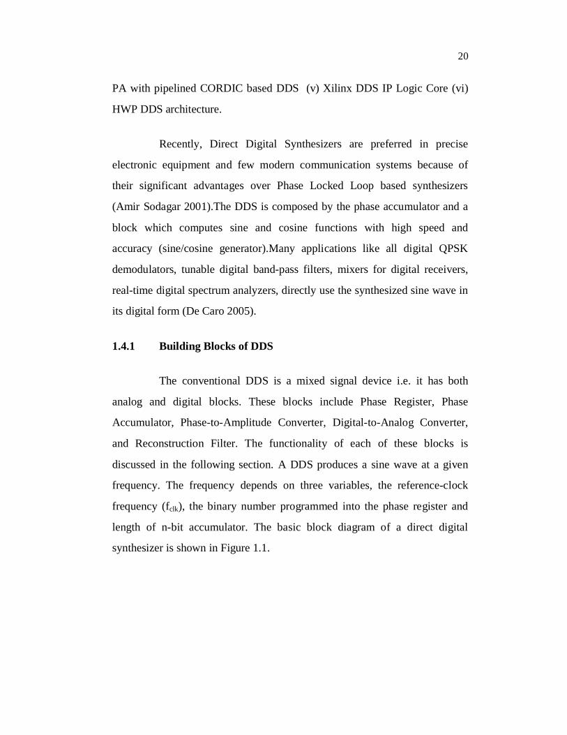
1.4.1 Building Blocks of DDS
The conventional DDS is a mixed signal device i.e. it has both
analog and digital blocks. These blocks include Phase Register, Phase
Accumulator, Phase-to-Amplitude Converter, Digital-to-Analog Converter,
and Reconstruction Filter. The functionality of each of these blocks is
discussed in the following section. A DDS produces a sine wave at a given
frequency. The frequency depends on three variables, the reference-clock
frequency (fclk), the binary number programmed into the phase register and
length of n-bit accumulator. The basic block diagram of a direct digital
synthesizer is shown in Figure 1.1.
21
PhaseAccumulator
FrequencyControlWord
fout
fclk
Figure 1.1 DDS functional Blocks and signal flow diagram
The binary number in the phase register provides the main input to
the phase accumulator. The binary number is also known as Frequency
Control Word.
If a sine look-up table is used, the phase accumulator computes a
phase (angle) address for the look-up table, which outputs the digital value of
the DAC, in turn it converts that number to a corresponding value of analog
voltage or current. To generate a fixed-frequency sine wave, the phase
increment is determined by the FCW is added to the phase accumulator with
each clock cycle. If the phase increment is large, the phase accumulator will
step quickly through the sine look-up table and thus generate a high frequency

22
sine wave. If the phase increment is small, the phase accumulator will take
more number of steps, accordingly generating a slower waveform (DDS
Technical Tutorial 1999).
1.4.2 Phase Accumulator
The phase accumulator consists of an-bit frequency register which
stores a digital phase increment word followed by a n-bit full adder and a
phase register. The digital input phase increment word is entered in the
frequency register. At each clock pulse this data is added to the data
previously held in the phase register. The phase increment word represents a
phase angle step that is added to the previous value at each 1/fclk seconds to
produce a linearly increasing digital value. The phase value is generated using
the modulo 2nproperty of a n-bit phase accumulator. The output frequency is
f = (1.1)
The Equation (1.1) is known as the DDS "tuning equation." fclk is
the clock frequency. The frequency resolution of the system equals fclk/2n. In a
practical DDS system, all the bits out of the phase accumulator are not passed
on to the LUT but are truncated. This reduces the size of the LUT and does
not affect the frequency resolution. The phase truncation only adds a small
but acceptable amount of phase noise to the final output (Sodagar et al 2001).
23
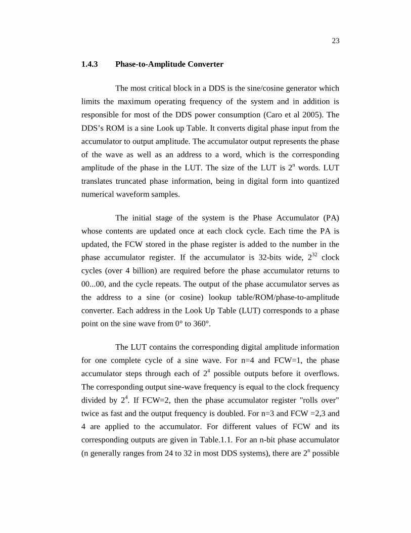
1.4.3 Phase-to-Amplitude Converter
The most critical block in a DDS is the sine/cosine generator whichlimits the maximum operating frequency of the system and in addition isresponsible for most of the DDS power consumption (Caro et al 2005). TheDDS’s ROM is a sine Look up Table. It converts digital phase input from theaccumulator to output amplitude. The accumulator output represents the phaseof the wave as well as an address to a word, which is the correspondingamplitude of the phase in the LUT. The size of the LUT is 2n words. LUTtranslates truncated phase information, being in digital form into quantizednumerical waveform samples.
The initial stage of the system is the Phase Accumulator (PA)whose contents are updated once at each clock cycle. Each time the PA isupdated, the FCW stored in the phase register is added to the number in thephase accumulator register. If the accumulator is 32-bits wide, 232 clockcycles (over 4 billion) are required before the phase accumulator returns to00...00, and the cycle repeats. The output of the phase accumulator serves asthe address to a sine (or cosine) lookup table/ROM/phase-to-amplitudeconverter. Each address in the Look Up Table (LUT) corresponds to a phasepoint on the sine wave from 0° to 360°.
The LUT contains the corresponding digital amplitude informationfor one complete cycle of a sine wave. For n=4 and FCW=1, the phaseaccumulator steps through each of 24 possible outputs before it overflows.The corresponding output sine-wave frequency is equal to the clock frequencydivided by 24. If FCW=2, then the phase accumulator register "rolls over"twice as fast and the output frequency is doubled. For n=3 and FCW =2,3 and4 are applied to the accumulator. For different values of FCW and itscorresponding outputs are given in Table.1.1. For an n-bit phase accumulator(n generally ranges from 24 to 32 in most DDS systems), there are 2n possible
24
phase points. The digital word FCW in the phase register represents theamount of the phase accumulator, incremented at each clock cycle.
Table 1.1 Accumulator of 3 bits (n=3) controlled with an input of
FCW= 2, 3 and 4
Accumulatoroutput
n=3, FCW=2
Carryoutput
Accumulatoroutput
n=3, FCW=3
Carryoutput
Accumulatoroutput
n=3, FCW=4
Carryoutput
000(0) 1(Cyclebegins)
000(0) 1(Cyclebegins)
000(0) 1(Cyclebegins)
010(2) 0 011(3) 0 100(4) 0
100(4) 0 110(6) 0 001(1) 1110(6) 0 011(1) 1 101(5) 0000(0) 1 100(4) 0 010(2) 1010(2) 0 101(7) 0 110(6) 0100(4) 0 110(2) 1 011(3) 1110(6) 0 111(5) 0 111(7) 0000(0) 1 000(0) 1 011(3) 1
Phase truncation is an important aspect of DDS architectures.
Consider a DDS with a 32-bit phase accumulator. To directly convert 32 bits
of phase to corresponding amplitude would require 232 entries in a lookup
table. That is 4,294,967,296 entries. If each entry is stored with 8-bit
accuracy, then 4-Gigabytes of lookup table memory would be required.
Clearly, it would be impractical to implement such a design.
Hence the solution is to use a fraction of the most significant bits of
the accumulator output to provide phase information. For example, In a 32-bit
DDS design, only the upper most bits might be used for phase information.
The lower bits would be ignored (truncated) in this case. To understand the
25
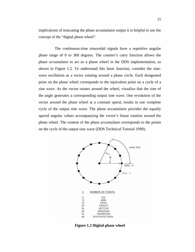
implications of truncating the phase accumulator output it is helpful to use the
concept of the “digital phase wheel”.
The continuous-time sinusoidal signals have a repetitive angular
phase range of 0 to 360 degrees. The counter’s carry function allows the
phase accumulator to act as a phase wheel in the DDS implementation, as
shown in Figure 1.2. To understand this basic function, consider the sine-
wave oscillation as a vector rotating around a phase circle. Each designated
point on the phase wheel corresponds to the equivalent point on a cycle of a
sine wave. As the vector rotates around the wheel, visualize that the sine of
the angle generates a corresponding output sine wave. One revolution of the
vector around the phase wheel at a constant speed, results in one complete
cycle of the output sine wave. The phase accumulator provides the equally
spaced angular values accompanying the vector’s linear rotation around the
phase wheel. The content of the phase accumulator corresponds to the points
on the cycle of the output sine wave (DDS Technical Tutorial 1999).
Figure 1.2 Digital phase wheel

26
1.5 FREQUENCY TUNING
A sine wave is generally expressed as x(t)= sin( t)which is non-
linear and is not easy to generate , except through constructing it from pieces.
However, the angular information is linear because the phase angle rotates
through a fixed angle for each unit of time. Thus, the angular rate depends on
the frequency of the signal described as =2 f where is the angular
frequency. As shown in Figure 1.3, the phase increases linearly from 0 to 2
over one complete cycle of the sine wave.
Figure 1.3 Representation of sine magnitude and phase
The phase of a sine wave is linear and that it depends on a reference
clock period, with clock frequency (f ), the phase rotation (Pr) for that
period can be determined by
P = t (1.2)
Where Pr is change in phase of sine wave, = angular frequency of wave, t
is small change in time. Solving for in Equation (1.2), gives
= (P | t) = 2 f (1.3)
27
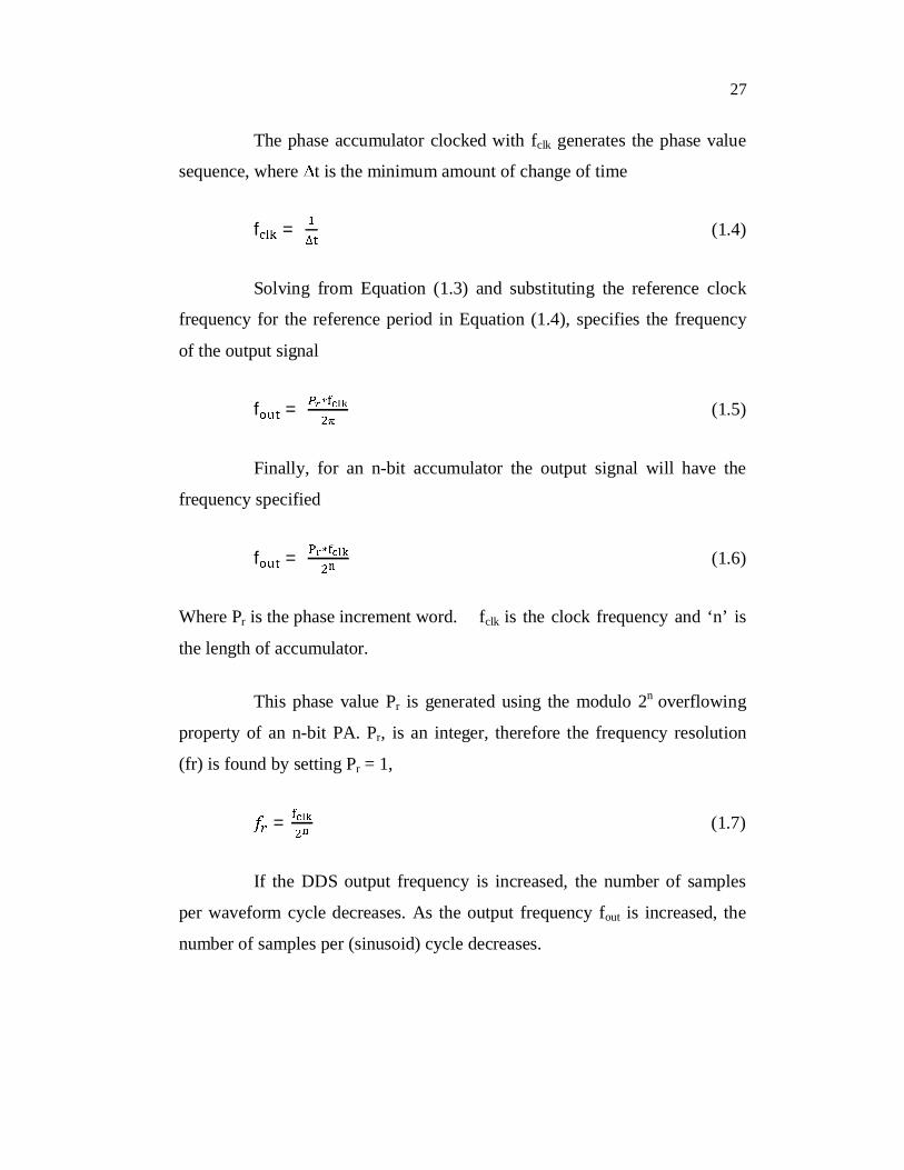
The phase accumulator clocked with fclk generates the phase value
sequence, where t is the minimum amount of change of time
f = (1.4)
Solving from Equation (1.3) and substituting the reference clock
frequency for the reference period in Equation (1.4), specifies the frequency
of the output signal
f = (1.5)
Finally, for an n-bit accumulator the output signal will have the
frequency specified
f = (1.6)
Where Pr is the phase increment word. fclk is the clock frequency and ‘n’ is
the length of accumulator.
This phase value Pr is generated using the modulo 2n overflowing
property of an n-bit PA. Pr, is an integer, therefore the frequency resolution
(fr) is found by setting Pr = 1,
= (1.7)
If the DDS output frequency is increased, the number of samples
per waveform cycle decreases. As the output frequency fout is increased, the
number of samples per (sinusoid) cycle decreases.
28
1.6 DDS DESIGN FEATURES
The current SDR implementations mostly rely on reconfigurable
hardware to support a particular standard or waveform while the algorithms
and the various setups for other waveforms are stored in memory. Although
application-specific integrated circuits lead to the most efficient
implementation of a single-standard radio, the same cannot be said when
addressing a multi-mode multi-standard device. The ASIC is a very complex
approach in terms of implementation and inefficient in terms of cost and
power consumption (Rouphael 2009). The present work might be a solution
which is obtained using Xilinx Spartan FPGA to develop the novel DDS
architecture.
1.6.1 FPGA Design Methodology
FPGA devices are an important component in many modern
devices. It is important that VLSI designers must have a thorough knowledge
of optimizing designs for FPGAs. When using an FPGA it is common to use
VHDL or VerilogHDL to describe the functionality of the FPGA. Specialized
software tools are used to translate the HDL source code into a configuration
bit stream for the FPGA. It instructs the configurable elements in the FPGA.
Traditionally, FPGA consists of two main parts: routing and
Configurable Logic Blocks (CLB). A CLB typically contains a small amount
of logic that can be configured to perform Boolean operations on the inputs to
the CLB block. The logic can be constructed by using a small memory that is
used as a lookup table. This is often referred to as a LUT. The logic in the
CLB block is connected to a small number of flip-flops in the CLB block. The
CLBs are also connected to switch matrices that in turn are connected to each
other using a network of wires.
29
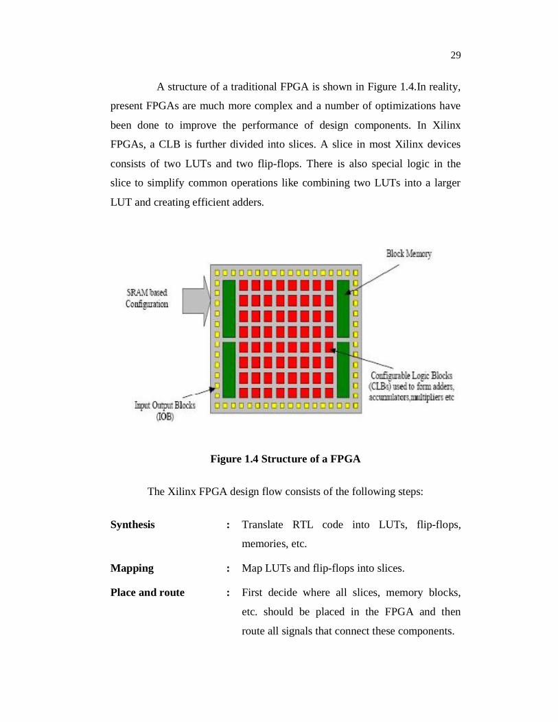
A structure of a traditional FPGA is shown in Figure 1.4.In reality,
present FPGAs are much more complex and a number of optimizations have
been done to improve the performance of design components. In Xilinx
FPGAs, a CLB is further divided into slices. A slice in most Xilinx devices
consists of two LUTs and two flip-flops. There is also special logic in the
slice to simplify common operations like combining two LUTs into a larger
LUT and creating efficient adders.
Figure 1.4 Structure of a FPGA
The Xilinx FPGA design flow consists of the following steps:
Synthesis : Translate RTL code into LUTs, flip-flops,
memories, etc.
Mapping : Map LUTs and flip-flops into slices.
Place and route : First decide where all slices, memory blocks,
etc. should be placed in the FPGA and then
route all signals that connect these components.

30
Bit file generation : Convert the net list produced by the place and
route step into a bit stream that can be used to
configure the FPGA.
FPGA Configuration : Download the bit stream into the FPGA.
A static timing analyser tool can be used to determine the critical
path of a present design. It can also be used to make sure that a design is
meeting the timing constraints but it’s seldom necessary as the place and route
tool will usually give a warning if the timing constraints are not met. There
are special tools available to inspect and modify the design. A floor planning
tool allows a designer to investigate the placement of all components in a
design and change the placement if necessary. FPGA editing tool can be used
to view and edit the exact configuration of a CLB and other components in
terms of logic equations for LUTs, flip-flop configuration, etc. It will also
show how signals are routed in the FPGA and can also change the routing if
necessary.
1.7 SPARTAN FPGA FEATURES
The Spartan family of Field-Programmable Gate Arrays is
specifically designed to meet the needs of high volume, cost-sensitive
consumer electronic applications. Spartan family is based on a 90nm, eight
layer metal processes, with densities up to 74K logic cells (LCs) and up to 1.8
Mbits of embedded RAM, with dedicated 18 × 18 multipliers, up to 4 Digital
Clock Managers (DCM), and high-speed, versatile external RAM interface.
Spartan devices support differential and single-ended I/O standards.
The Spartan-6 LX45 is optimized for high performance logic and
offers:
31
• 6,822 slices, each containing four 6- input LUTs and eight
flip-flops
• six phase-locked loops
• 58 DSP slices
• 500MHz clock speeds
1.8 OPTIMIZING A DESIGN FOR FPGAS
(i) High-Level Optimization
The simple way to increase the performance in FPGAs is adding
pipeline-stages. It is usually a special area efficient in FPGAs. Another way to
improve the performance of an FPGA is by utilizing all capabilities of the
embedded memories. In FPGAs, the basic memory block primitive is usually
dual-ported by default as it will simplify an algorithm. Similarly, each
memory block in an FPGA has a fixed size.
(ii) Low level optimization
In the high level optimizations the performance obtained is not
satisfactory as it is not possible to fine-tune the architecture for a certain
FPGA. In low level optimization the design can be fine tuned to make sure
that the algorithms are mapped to the FPGA in such a way that adders can be
efficiently combined with other components such as multiplexers and gates
while keeping the number of logic levels low.

32
(iii) Placement Optimizations
If the required performance is not reached through either high or
low level logic optimizations it is usually possible to gain more performance
by floor planning.
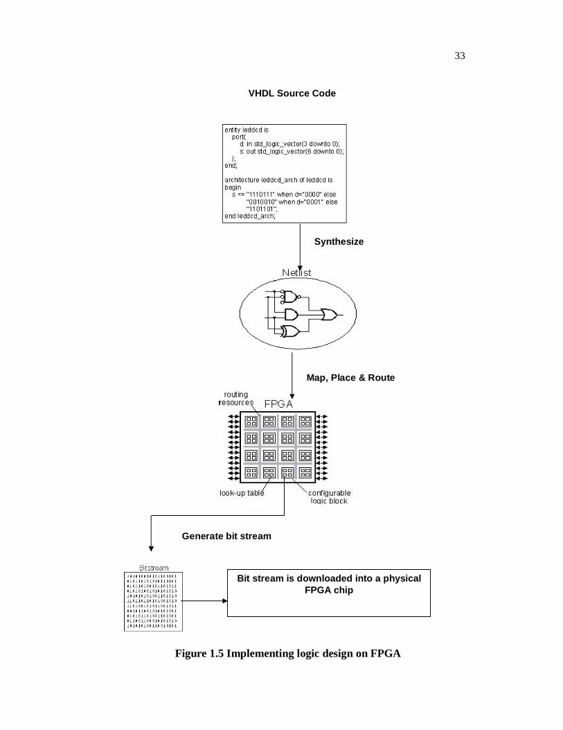
1.9 FPGA DESIGN FLOW
In a typical design flow, FPGA application developer will simulate
the design at multiple stages throughout the design process. Initially the RTL
description in VHDL or Verilog HDL is simulated by creating test benches to
stimulate the system and observe results.
Then, after the synthesis engine is mapped the design to a net list,
the net list is translated to a gate level description where simulation is
repeated to confirm the synthesis proceeded without errors. Finally, the design
is laid out in the FPGA at which point propagation delays are added and the
simulation is run again with these values back-annotated onto the net list.
33
Figure 1.5 Implementing logic design on FPGA
Synthesize
Map, Place & Route
Generate bit stream
Bit stream is downloaded into a physicalFPGA chip
VHDL Source Code

34
1.10 ORGANIZATION OF THESIS
This thesis is organized as follows.
CHAPTER 1 : Problem formulation, Motivation and Objectives for the
present research work are clearly stated. Literature
survey is extensively discussed.
CHAPTER 2 : Implementations of Pipelined Carry Look Ahead Phase
Accumulator and ROM Look up Table for DDS
architecture are described. The performance of Pipelined
DDS architecture is compared with Non-pipeline DDS.
Implementation and simulation results are discussed.
CHAPTER 3 : Hybrid Wave pipelining Technique for Phase
Accumulator has been explained. Comparison with
conventional pipeline and hybrid wave pipeline scheme
is also provided.
CHAPTER 4 : Comparison of different CORDIC architectures has been
analyzed. HWP CORDIC algorithm technique to
improve area efficiency is presented.
CHAPTER 5 : HWP based DDS architecture is implemented on to the
reconfigurable hardware and results are discussed.
Performance of various DDS architecture are compared
and analyzed.
CHAPTER 6 : Conclusion and the directions for the future work is
presented and followed by references are listed.