Embed Size (px)
Citation preview
Claudio Piemonte RD50 workshop CERN, 14-16 November 2005
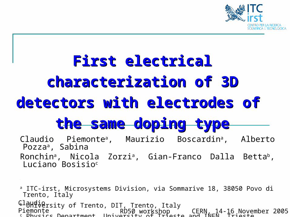
Claudio Piemontea, Maurizio Boscardina, Alberto Pozzaa, SabinaRonchina, Nicola Zorzia, Gian-Franco Dalla Bettab, Luciano Bosisioc
\
a ITC-irst, Microsystems Division, via Sommarive 18, 38050 Povo di Trento, Italy b University of Trento, DIT, Trento, Italy
c Physics Department, University of Trieste and INFN, Trieste, Italy
First electrical characterization First electrical characterization
of 3D detectors with electrodes of 3D detectors with electrodes
of the same doping typeof the same doping type
Claudio Piemonte RD50 workshop CERN, 14-16 November 2005
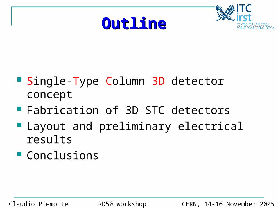
Single-Type Column 3D detector concept Fabrication of 3D-STC detectors Layout and preliminary electrical results Conclusions
OutlineOutline

Claudio Piemonte RD50 workshop CERN, 14-16 November 2005
STC-3D detectors - concept (1)STC-3D detectors - concept (1)
Sketch of the detector:
grid-like bulk contact
ionizing particle
cross-sectionbetween twoelectrodes
n+ n+
electrons are swept away by the transversalfield
holes drift in the central region and diffuse towards p+contact
n+-columns
p-type substrate
Adv. over standard 3D: etching and column doping performed only once
Functioning:
[C. Piemonte et al, Nucl. Instr. Meth. A 541 (2005)]

Claudio Piemonte RD50 workshop CERN, 14-16 November 2005
3DSTC detectors - concept (2)3DSTC detectors - concept (2)
Further simplification: holes not etched all through the wafer
p-type substraten+ electrodes
Uniform p+ layer
Bulk contact is provided by a backsideuniform p+ implant single side process.
No need of support wafer.

Claudio Piemonte RD50 workshop CERN, 14-16 November 2005
Potential distribution(vertical cross-section)
Potential distribution(horizontal cross-section)
null field regions0V
-10V
-5V
50m
300
m
-15VDrawbacks: • once full depletion is reached it is not possible to increase the electric field between the columns• large low field region
3DSTC detectors - 3D simulations3DSTC detectors - 3D simulations
Both can be improved using higher substrate doping concentration

Claudio Piemonte RD50 workshop CERN, 14-16 November 2005
Fabrication process (1)Fabrication process (1)
n+ diffusion
contact
metal
oxide
hole
MAIN STEPS:
1. Hole etching with Deep RIE machine (step performed at CNM, Barcelona, Spain)
2. n+ diffusion (column doping)
3. passivation of holes with oxide4. contact opening5. metallization
10 m
Hole depth: 120μm
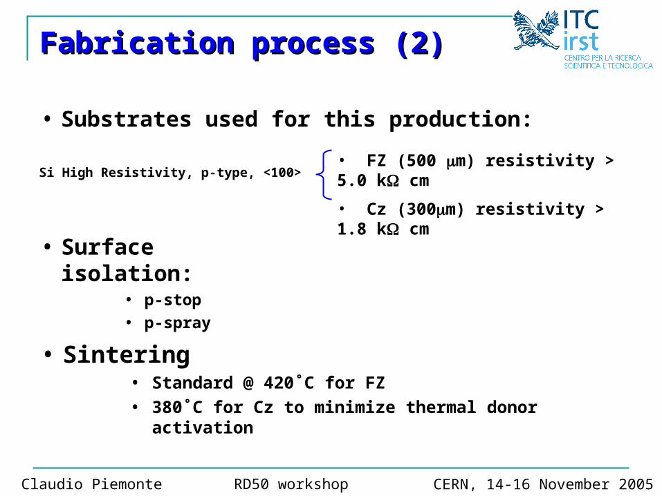
CHOICES FOR THIS PRODUCTION:
• No hole filling (with polysilicon)• Holes are not etched all through the wafer• Bulk contact provided by a uniform p+ implant
Claudio Piemonte RD50 workshop CERN, 14-16 November 2005
Si High Resistivity, p-type, <100>
• Surface isolation:• p-stop
• p-spray
• FZ (500 m) resistivity > 5.0 k cm
• Cz (300m) resistivity > 1.8 k cm
• Substrates used for this production:
• Sintering• Standard @ 420˚C for FZ
• 380˚C for Cz to minimize thermal donor activation
Fabrication process (2)Fabrication process (2)

Claudio Piemonte RD50 workshop CERN, 14-16 November 2005
Mask layoutMask layout
Small version of strip detectors
Planar and 3D test structures
“Low density layout”to increase mechanicalrobustness of the wafer
“Large” strip-like detectors

Claudio Piemonte RD50 workshop CERN, 14-16 November 2005
Planar test structures measurementsPlanar test structures measurements
Standard planar test structures
Electrical parameters compatible with standard planar processes
High variation due to different substrates
Ileak measured below full depletion due to Vbreak
Parameter Unitp-spray p-stop
Na [1E12 cm-3]Vdep [V]Ileak [nA/cm2]Vbreak [V] 60 - 140 155 - 175Tox [nm] 570 - 585 860 - 875Qox [1E10cm-2] 9.5 - 11 6 - 9.6So [cm/s] 1.3 - 1.7 7 - 7.5
typical range
1 - 3.5200 - 500
1 - 2050 - 60
Claudio Piemonte RD50 workshop CERN, 14-16 November 2005
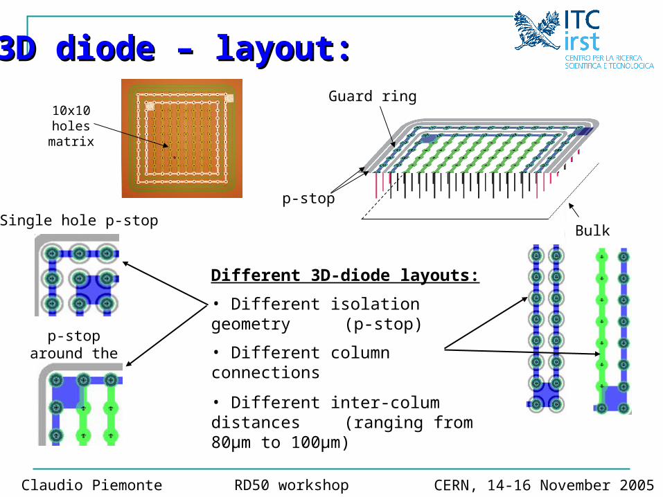
3D diode – layout:3D diode – layout:
Different 3D-diode layouts:
• Different isolation geometry (p-stop)
• Different column connections
• Different inter-colum distances (ranging from 80μm to 100μm)
Bulk
Guard ring
p-stop
10x10 holes matrix
Single hole p-stop
p-stop around the entire region
Claudio Piemonte RD50 workshop CERN, 14-16 November 2005
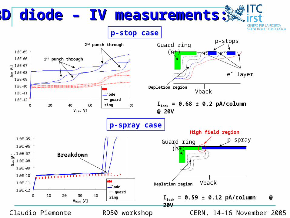
3D diode – IV measurements:3D diode – IV measurements:
Vback
Guard ring (n+) p-spray
Depletion region
High field region
diode
─ guard ring
1.0E-12
1.0E-11
1.0E-10
1.0E-09
1.0E-08
1.0E-07
1.0E-06
1.0E-05
1.0E-04
0 20 40 60 80 100Vbias [V]
I lea
k [
A]
p-stop case
diode
─ guard ring
1st punch through
2nd punch through
1.0E-12
1.0E-11
1.0E-10
1.0E-09
1.0E-08
1.0E-07
1.0E-06
1.0E-05
1.0E-04
0 10 20 30 40 50 60Vbias [V]
I lea
k [A
]
diode
─ guard ring
p-spray case
Breakdown
Vback
Guard ring (n+)p-stops
e- layer
- -
Depletion region
Ileak = 0.68 ± 0.2 pA/column @ 20V
Ileak = 0.59 ± 0.12 pA/column @ 20V

Claudio Piemonte RD50 workshop CERN, 14-16 November 2005
3D diode – CV measurements3D diode – CV measurements (preliminary)(preliminary)
Capacitance measurement versus back on a 300m thick wafer with ~150m deep columns, 100m picth
Back
1/C2
0
2
4
6
8
10
12
0 10 20 30 40 50 60
Vbias [V]
Cd
iod
e [p
F]
0.00
0.50
1.00
1.50
2.00
2.50
0 10 20 30 40 50 60
Vbias [V]
C-2
[p
F-2
]
1 2
Phase 1
Phase 2
region between col.is not fully depleted large capacitance
full dep. between columns~ 7V
region between col.is fully depleted depletion proceedsonly towards the back(almost like a planar diode)
full depletion ~40Vdepletion width of ~150m
Cd
1/C
d2 [
pF
-2]
Cd
[pF
]
f=10kHz
Claudio Piemonte RD50 workshop CERN, 14-16 November 2005
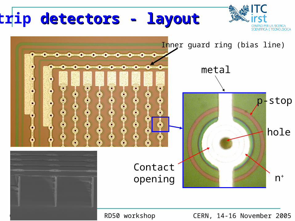
Strip detectors - layout detectors - layout
metal
p-stop
hole
Contact opening n+
Inner guard ring (bias line)

Claudio Piemonte RD50 workshop CERN, 14-16 November 2005
• Two different p-stop layouts:
Strip detectors – layout:Strip detectors – layout:
Different strip-detector layouts:
• Number of columns ranging from 12000 to 15000 • Inter-columns pitch 80-100 m• Holes Ø 6 or 10 m
Single p-stop for each hole
Common p-stop for each strip
Punch-through structures
• AC coupling: • DC coupling:
DC pads
Claudio Piemonte RD50 workshop CERN, 14-16 November 2005
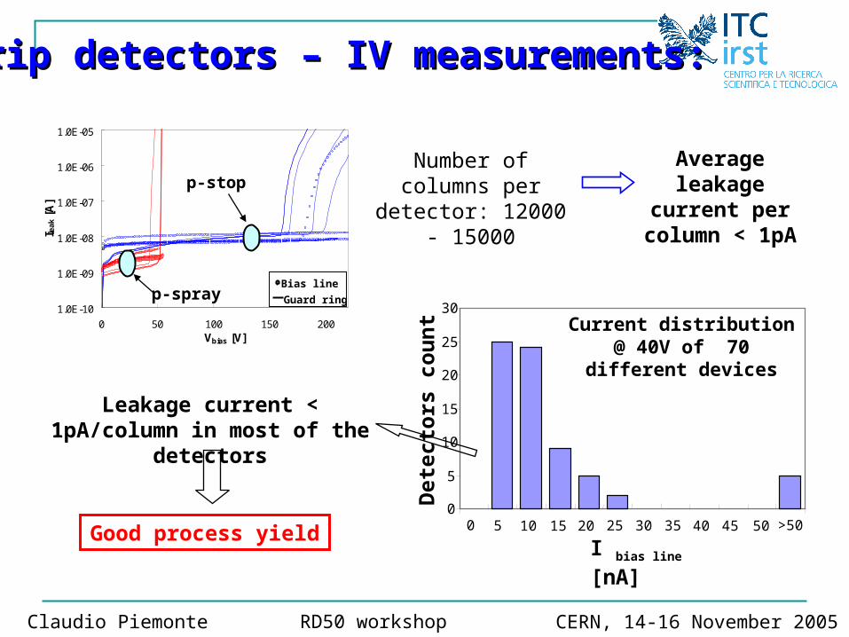
Current distribution @ 40V of 70 different devices
Good process yield
Strip detectors – IV measurements:Strip detectors – IV measurements:
1.0E-10
1.0E-09
1.0E-08
1.0E-07
1.0E-06
1.0E-05
0 50 100 150 200Vbias [V]
I lea
k [A
]
p-spray
p-stop
Bias line
Guard ring
Average leakage current per
column < 1pA
Number of columns per detector: 12000 -
15000
0
5
10
15
20
25
30
0 5 10 15 20 25 30 35 40 45 50 >50
I bias line [nA]
Det
ecto
rs c
ou
nt
Leakage current < 1pA/column in most of the detectors

Claudio Piemonte RD50 workshop CERN, 14-16 November 2005
ConclusioConclusionn• The first production has proved:
The feasibility of 3D-stc detectors Low leakage currents (< 1pA/column) Breakdown @ 50V for p-spray and >100V for p-stop structures Good process yield (typical detector current < 1pA/column)
• Samples have been given to: Glasgow (UK): CCE measurements with on 3D diodes
SCIPP (USA): CCE measurements on large strips

Claudio Piemonte RD50 workshop CERN, 14-16 November 2005
3D-stc TCAD 3D-stc TCAD simulationssimulationsSimulation of the electric field along a cut-line from the electrode to the center of the cell
Na=1e12 1/cm3
Na=5e12 1/cm3
Na=1e13 1/cm3 DRAWBACK:3D-stc: once full depletion is reached it is not possible to increase the electric field between the columns
Maximum electric field depends on substrate doping