Embed Size (px)
Citation preview

Book-to-Bill RatioFORJULY .83
MEMBER COMPANY PROFILE
Promex Industries Inc. has been a Silicon Valley microelectronics manufacturing services provider for over thirty years. Originally focused upon providing engi-neering build prototyping services to the local Silicon Valley community, Promex has outgrown those humble beginnings to become a full service IC Assembly & Cus-tom Chip Packaging Foundry. What makes Promex unique is its ability to enable their customers to take new products to market faster than by any other route. page 10
Semiconductor equipment bookings decrease 3% over June 2008 level. page 20
P romex’s customer base includes the major multi-national semiconductor companies, fab-less semi-
conductor houses, high tech start-ups and emerging high tech compa-nies. End-use markets include both commercial and military electron-ics as well as, RF, bio-tech, bio-met-ric, PV solar and optoelectronics products.
A Publication of The MicroElectronics Packaging & Test Engineering Council
One Day Technical Symposium and Exhibits Coming to San Jose, CA November 13th ... page 4
www.meptec.org Q3 2008 / MEPTEC Report 1
INDUSTRY NEWS
STATS ChipPAC Ltd. has announced an inno-vative USB module for NAND flash memory applications. page 15
Pac Tech Packaging Technologies held a grand opening celebration on September 18 at its new 55,000 square foot facility in Penang, Malaysia. The new facility provides state-of-the-art wafer bumping and backend process-ing for semiconductor companies within the Pacific Rim. page 16
Rudolph Technologies, Inc. has announced the receipt of orders from a major European semi-conductor manufacturer for two WaferWoRx® 300 Probing Process Analysis Systems.page 19
SEMI projects an over 20 percent increase in world semiconductor fab equipment spending in 2009, driven by over seventy fab projects, according to their World Fab Forecast report.page 21
The 5th Annual International Wafer-Level Pack-aging Conference returns to San Jose October 13 through 16. page 13
Volume 12, Number 3
QUARTER THREE 2008
Celebrating MEPTEC’s 30th Anniversary
Packaging Developments and InnovationsFrom System Design to Integrated Delivery

consistent quality
Contact Honeywell for solutions to your puzzle…visit www.honeywell.com/sm/em or call 1-408-962-2000.
© 2007 Honeywell International Inc. All rights reserved.
Six Sigma, metrics, unified operating systems…we leverage the appropriate tools and processes to ensure that our products meet or exceed your quality requirements.
Honeywell’s ongoing research and development in chemistry,
metallurgy, and the processes that bring them together—from
our new packaging R&D facility in Spokane, Washington, to our
technology center in Shanghai, China—ensure that wherever challenges arise, we’ll continue
to create solutions that solve them. And as a partner to most of the top semiconductor
houses worldwide, our technology portfolio is consistently at the forefront of invention,
empowering the global leaders of innovation. Honeywell Electronic Materials—because
the quality of your products depends upon ours.
Consistency-MR-Q308.indd 1 8/18/08 2:32:39 PM
Summer always seems to go by so quickly, and as this issue is being distributed it is officially the beginning of autumn. After taking a couple of months off, September marks our luncheon series kick-off with
Gartner-Dataquest’s traditional state-of-the-indus-try report. In both Sunnyvale and Phoenix, Mark Stromberg spoke on 2009: Return to Industry Growth or a Repeat of 2008? For a copy of this pre-sentation please contact [email protected]. Our first post-summer event was our 3rd Annual Medical Electronics Symposium, with emphasis on technology concepts that enable product reality. Arizona State University and Connection One (Ira A. Fulton School of Engineering) hosted the event at the historic Old Main building on the Tempe campus. We’d like to thank ASU for their great sup-port in putting this event together. If you missed it, CDs of the presentations will be available — contact MEPTEC for information on ordering. We’re also pleased to be offering a new series of MEMS Workshops, in conjunction with MEMS Investor Journal. On October 22 the first workshop will be held at the Ramada Inn in Sunnyvale called MEMS Testing and Reliability: Lessons Learned from the MEMS and Semiconductor Industries. See below for more information on this event. This issue will be distributed at our Q4 one-day technical symposium being held on November 13, 2008 at the Wyndham Hotel in San Jose, Califor-nia. The symposium is entitled “Packaging Devel-opments and Innovations: From System Design to Integrated Delivery”. We are celebrating our 30th anniversary with this event by teaming up with Advanced Packaging Magazine as co-sponsors. See page 4 for information. One of our feature articles this issue is from MEPTEC member company Bayside Design, Inc. In “Fundamental Challenges in High-Performance Package Design”, Daniel Lambalot, Director of Engineering at Bayside, discusses the challenges engineers face when designing a first-pass working package. Read this informative, thorough report on page 22. The other feature article is again from a MEPTEC member company, SemiProbe. Don Feuerstein discusses “Why 3D Interconnect and New SiP Pack-aging Schemes are Demanding KGD for MEMS
Devices” (see page 26). Don starts out by men-tioning that the creator of Moore’s Law, Gordon Moore, admits that the physical limits of his law are rapidly approaching. Don then goes into the reasons that make supplying MEMS KGD important. We’d like to thank both authors for their feature article contributions. Our University profile this issue is the Univer-sity of Colorado – iMint (Integrated Micro/Nano-Electromechanical Transducers) Center. The Center includes collaboration with many different entities, including universities, government agencies, and industry businesses. Several revolutionary discover-ies and inventions have resulted from the Center. One of the most interesting is Graphene – a material so strong that “it would take the weight of a two-ton car to puncture a sheet as thick as ordinary food wrap”. Read about “the stuff of science fiction” on page 8. Our Industry Analysis this issue is from Yole Développement on “3-D TSV Interconnects – The Next Revolution for Semiconductor Packaging and Circuit Assembly Industries” (page 5). They present their latest market forecast evaluating the impact of 3-D TSV technologies on several different segments of the semiconductor industry. Phil Marcoux, MEPTEC Advisory Board mem-ber and Director of Business Development at TPL Group contributed the editorial to this issue. In “Is it Time to Leave Solder?”, Phil offers his opinion on how the elimination of solder may solve many problems, one of which is a means to avoid the risks faced by the use of no-lead solder. Read his interest-ing and provocative piece on page 34. Our Member Company Profile this issue is from Corporate MEPTEC member Promex Industries Inc. Founded over 30 years ago, Promex began by providing engineering built prototyping services that serviced mostly the local Silicon Valley community. Over the years they have evolved into a full service IC assembly and custom chip packaging foundry serving customers worldwide. See page 10 for the profile of “Silicon Valley’s Packaging Foundry”. Thanks to all of our contributors for making this a great issue. If you’re reading our publication for the first time at one of the many events where we distribute, or if you’re a new member, we hope you enjoy it. Thanks for joining us! ◆
Council UpdateVolume 12, Number 3
A Publication of The MicroElectronics Packaging
& Test Engineering Council
P. O. Box 222Medicine Park, OK 73557
Tel: (650) 714-1570 Email: [email protected]
Published ByMEPCOM
EditorBette Cooper
Design and ProductionGary Brown
––––––––––––––MEPTEC Advisory Board
Seth AlaviSunSil
Jeffrey BradenLV Sensors, Inc.
Philippe BriotP. Briot & Associates
Joel CamardaExar Corporation
Gary CatlinPlexus
Tom Clifford
Rob Cole
John CraneJ. H. Crane & Associates
Jeffrey C. DemminTessera
Bruce EuzentAltera Corporation
Skip Fehr
Julia GoldsteinAdvanced Packaging Magazine
Anna GualtieriElle Technology
Bance HomConsultech International, Inc.
Ron JonesN-Able Group International
Nick LeonardiPremier Semiconductor Services
Phil MarcouxTPL Group
Bhavesh MuniHenkel Corporation
Mary OlssonGary Smith EDA
Marc PapageorgeSemiconductor Outsourcing Solutions
Rich RiceASE (US) Inc.
Jim WalkerGartner Dataquest
Russ WinslowSix Sigma
––––––––––––––
MEPTEC Report Vol. 12, No. 3. Published quarterly by MEPCOM, P. O. Box 222, Medicine Park, OK 73557. Copyright 2008 by MEPTEC/MEPCOM. All rights reserved. Materials may not be reproduced in whole or in part without written permission.
MEPTEC Report is sent without charge to members of MEPTEC. For non-members, yearly subscriptions are avail-able for $75 in the United States, $80US in Canada and Mexico, and $95US elsewhere.
For advertising rates and information contact John Waller at 215-646-7838, Fax 215-646-0504.
www.meptec.org Q3 2008 / MEPTEC Report 3
MEMS Testing and Reliability WorkshopOn October 22 a workshop will be held at the Ramada Inn in Sunnyvale titled MEMS Testing and Reli-ability: Lessons Learned from the MEMS and Semiconductor Industries. MEMS testing and reliability assurance are some of the most critical processes to ensure high yields and profitability. According to recent studies, the total world MEMS test equipment market generated revenues of $50-$60 million in 2007, at a growth rate of approximately 10 percent. While MEMS test-ing is similar to chip testing in the semiconductors industry, MEMS devices present further challenges because mechanical, chemical and optical parameters must be tested in addition to electrical properties. MEMS foundries and even fabless MEMS companies need to ensure that they have in-house expertise in MEMS testing and reliability. This workshop will ensure that your organization stays current with the latest MEMS testing and reliability trends and therefore decrease waste while increasing yields and profitability. The workshop will include a luncheon presentation by Dr. Leslie Field, Founder and Managing Member of SmallTech Consulting on Packaging of BioMEMS.
Go to www.meptec.org for complete program details and pricing.

R E G I S T E R O N L I N E T O D A Y A T W W W . M E P T E C . O R G
A O N E - D A Y T E C H N I C A L S Y M P O S I U M & E X H I B I T S
MEPTEC & Advanced Packaging Magazine Present
Celebrating MEPTEC’s 30th Anniversary
Packaging Developments and InnovationsFrom System Design to Integrated DeliveryNovember 13, 2008 Wyndham Hotel • San Jose, California
MEDIA SPONSORS
S A N J O S E
Sessions will include:
n Advanced Packages and Processes
n Packaging to Board Assembly Trends
n Design Tools and Co-Design Solutions
n Microelectronics Substrate Fabrication and Assembly Innovations
DIAMOND SPONSOR
PLATINUM SPONSOR
SILVER SPONSORS
GOLD SPONSOR
MEPTEC Industry Analysis
T he Semiconductor manufactur-ing industry is today facing more than ever the challenge to explore the so-called “More-than-Moore” 3-D integration route in order
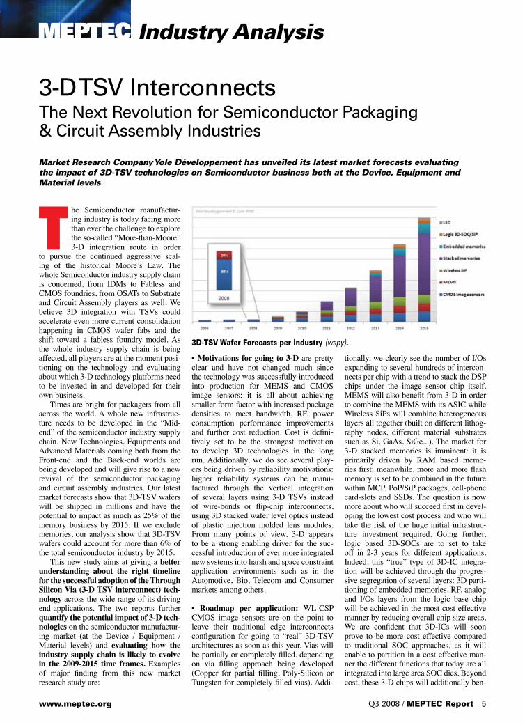
to pursue the continued aggressive scal-ing of the historical Moore’s Law. The whole Semiconductor industry supply chain is concerned, from IDMs to Fabless and CMOS foundries, from OSATs to Substrate and Circuit Assembly players as well. We believe 3D integration with TSVs could accelerate even more current consolidation happening in CMOS wafer fabs and the shift toward a fabless foundry model. As the whole industry supply chain is being affected, all players are at the moment posi-tioning on the technology and evaluating about which 3-D technology platforms need to be invested in and developed for their own business. Times are bright for packagers from all across the world. A whole new infrastruc-ture needs to be developed in the “Mid-end” of the semiconductor industry supply chain. New Technologies, Equipments and Advanced Materials coming both from the Front-end and the Back-end worlds are being developed and will give rise to a new revival of the semiconductor packaging and circuit assembly industries. Our latest market forecasts show that 3D-TSV wafers will be shipped in millions and have the potential to impact as much as 25% of the memory business by 2015. If we exclude memories, our analysis show that 3D-TSV wafers could account for more than 6% of the total semiconductor industry by 2015. This new study aims at giving a better understanding about the right timeline for the successful adoption of the Through Silicon Via (3-D TSV interconnect) tech-nology across the wide range of its driving end-applications. The two reports further quantify the potential impact of 3-D tech-nologies on the semiconductor manufactur-ing market (at the Device / Equipment / Material levels) and evaluating how the industry supply chain is likely to evolve in the 2009-2015 time frames. Examples of major finding from this new market research study are:
• Motivations for going to 3-D are pretty clear and have not changed much since the technology was successfully introduced into production for MEMS and CMOS image sensors: it is all about achieving smaller form factor with increased package densities to meet bandwidth, RF, power consumption performance improvements and further cost reduction. Cost is defini-tively set to be the strongest motivation to develop 3D technologies in the long run. Additionally, we do see several play-ers being driven by reliability motivations: higher reliability systems can be manu-factured through the vertical integration of several layers using 3-D TSVs instead of wire-bonds or flip-chip interconnects, using 3D stacked wafer level optics instead of plastic injection molded lens modules. From many points of view, 3-D appears to be a strong enabling driver for the suc-cessful introduction of ever more integrated new systems into harsh and space constraint application environments such as in the Automotive, Bio, Telecom and Consumer markets among others.
• Roadmap per application: WL-CSP CMOS image sensors are on the point to leave their traditional edge interconnects configuration for going to “real” 3D-TSV architectures as soon as this year. Vias will be partially or completely filled, depending on via filling approach being developed (Copper for partial filling, Poly-Silicon or Tungsten for completely filled vias). Addi-
tionally, we clearly see the number of I/Os expanding to several hundreds of intercon-nects per chip with a trend to stack the DSP chips under the image sensor chip itself. MEMS will also benefit from 3-D in order to combine the MEMS with its ASIC while Wireless SiPs will combine heterogeneous layers all together (built on different lithog-raphy nodes, different material substrates such as Si, GaAs, SiGe...). The market for 3-D stacked memories is imminent: it is primarily driven by RAM based memo-ries first; meanwhile, more and more flash memory is set to be combined in the future within MCP, PoP/SiP packages, cell-phone card-slots and SSDs. The question is now more about who will succeed first in devel-oping the lowest cost process and who will take the risk of the huge initial infrastruc-ture investment required. Going further, logic based 3D-SOCs are to set to take off in 2-3 years for different applications. Indeed, this “true” type of 3D-IC integra-tion will be achieved through the progres-sive segregation of several layers: 3D parti-tioning of embedded memories, RF, analog and I/Os layers from the logic base chip will be achieved in the most cost effective manner by reducing overall chip size areas. We are confident that 3D-ICs will soon prove to be more cost effective compared to traditional SOC approaches, as it will enable to partition in a cost effective man-ner the different functions that today are all integrated into large area SOC dies. Beyond cost, these 3-D chips will additionally ben-
3-D TSV InterconnectsThe Next Revolution for Semiconductor Packaging& Circuit Assembly Industries Market Research Company Yole Développement has unveiled its latest market forecasts evaluating the impact of 3D-TSV technologies on Semiconductor business both at the Device, Equipment and Material levels
3D-TSV Wafer Forecasts per Industry (wspy).
www.meptec.org Q3 2008 / MEPTEC Report 5
MEPTEC Industry Analysis
6 MEPTEC Report / Q3 2008 www.meptec.org
efit from performance improvements as interconnect length will be shortened and repeaters will be removed. This will allow the CMOS industry to “virtually” go beyond the 32nm node in terms of chip size, cost and performance.
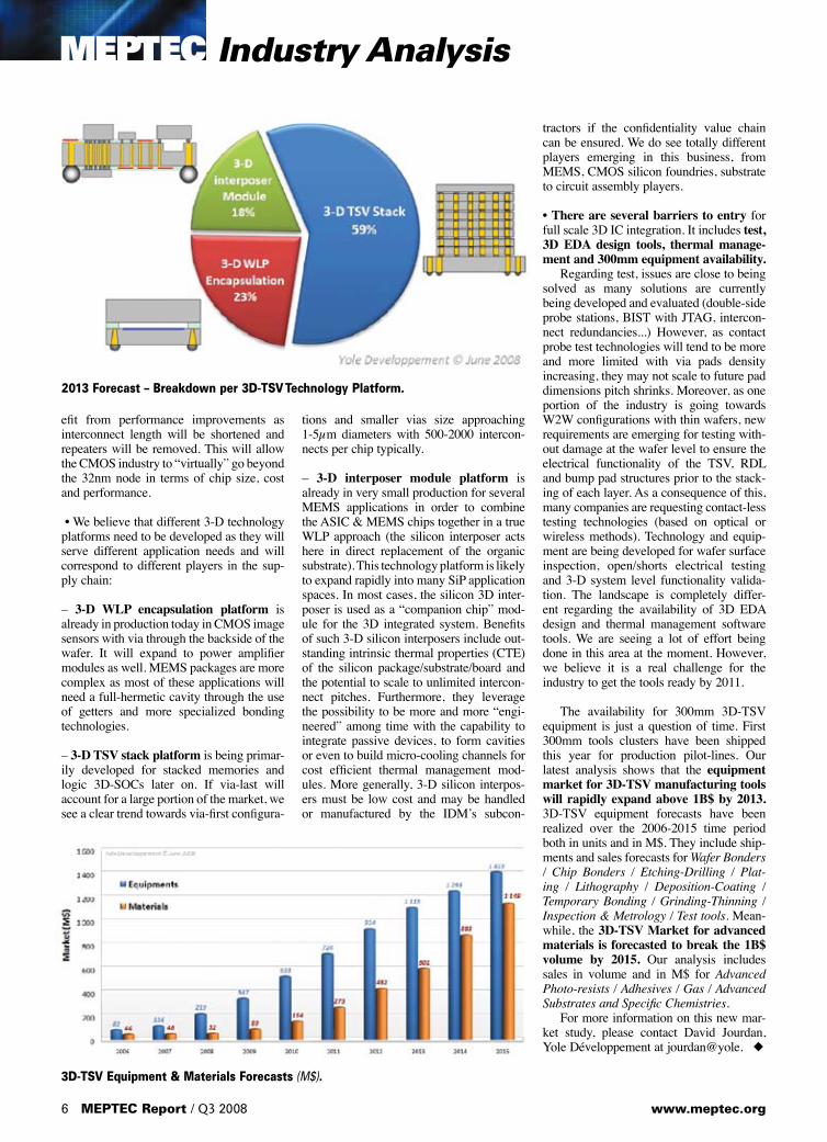
• We believe that different 3-D technology platforms need to be developed as they will serve different application needs and will correspond to different players in the sup-ply chain:
– 3-D WLP encapsulation platform is already in production today in CMOS image sensors with via through the backside of the wafer. It will expand to power amplifier modules as well. MEMS packages are more complex as most of these applications will need a full-hermetic cavity through the use of getters and more specialized bonding technologies.
– 3-D TSV stack platform is being primar-ily developed for stacked memories and logic 3D-SOCs later on. If via-last will account for a large portion of the market, we see a clear trend towards via-first configura-
tions and smaller vias size approaching 1-5µm diameters with 500-2000 intercon-nects per chip typically.
– 3-D interposer module platform is already in very small production for several MEMS applications in order to combine the ASIC & MEMS chips together in a true WLP approach (the silicon interposer acts here in direct replacement of the organic substrate). This technology platform is likely to expand rapidly into many SiP application spaces. In most cases, the silicon 3D inter-poser is used as a “companion chip” mod-ule for the 3D integrated system. Benefits of such 3-D silicon interposers include out-standing intrinsic thermal properties (CTE) of the silicon package/substrate/board and the potential to scale to unlimited intercon-nect pitches. Furthermore, they leverage the possibility to be more and more “engi-neered” among time with the capability to integrate passive devices, to form cavities or even to build micro-cooling channels for cost efficient thermal management mod-ules. More generally, 3-D silicon interpos-ers must be low cost and may be handled or manufactured by the IDM’s subcon-
tractors if the confidentiality value chain can be ensured. We do see totally different players emerging in this business, from MEMS, CMOS silicon foundries, substrate to circuit assembly players. • There are several barriers to entry for full scale 3D IC integration. It includes test, 3D EDA design tools, thermal manage-ment and 300mm equipment availability. Regarding test, issues are close to being solved as many solutions are currently being developed and evaluated (double-side probe stations, BIST with JTAG, intercon-nect redundancies...) However, as contact probe test technologies will tend to be more and more limited with via pads density increasing, they may not scale to future pad dimensions pitch shrinks. Moreover, as one portion of the industry is going towards W2W configurations with thin wafers, new requirements are emerging for testing with-out damage at the wafer level to ensure the electrical functionality of the TSV, RDL and bump pad structures prior to the stack-ing of each layer. As a consequence of this, many companies are requesting contact-less testing technologies (based on optical or wireless methods). Technology and equip-ment are being developed for wafer surface inspection, open/shorts electrical testing and 3-D system level functionality valida-tion. The landscape is completely differ-ent regarding the availability of 3D EDA design and thermal management software tools. We are seeing a lot of effort being done in this area at the moment. However, we believe it is a real challenge for the industry to get the tools ready by 2011.
The availability for 300mm 3D-TSV equipment is just a question of time. First 300mm tools clusters have been shipped this year for production pilot-lines. Our latest analysis shows that the equipment market for 3D-TSV manufacturing tools will rapidly expand above 1B$ by 2013. 3D-TSV equipment forecasts have been realized over the 2006-2015 time period both in units and in M$. They include ship-ments and sales forecasts for Wafer Bonders / Chip Bonders / Etching-Drilling / Plat-ing / Lithography / Deposition-Coating / Temporary Bonding / Grinding-Thinning / Inspection & Metrology / Test tools. Mean-while, the 3D-TSV Market for advanced materials is forecasted to break the 1B$ volume by 2015. Our analysis includes sales in volume and in M$ for Advanced Photo-resists / Adhesives / Gas / Advanced Substrates and Specific Chemistries. For more information on this new mar-ket study, please contact David Jourdan, Yole Développement at jourdan@yole. ◆
3D-TSV Equipment & Materials Forecasts (M$).
2013 Forecast – Breakdown per 3D-TSV Technology Platform.
Booth space available at gsaglobal.org/expo08
PLAT INUM SPONSORS
GOLD SPONSORS
MEDIA SPONSORS
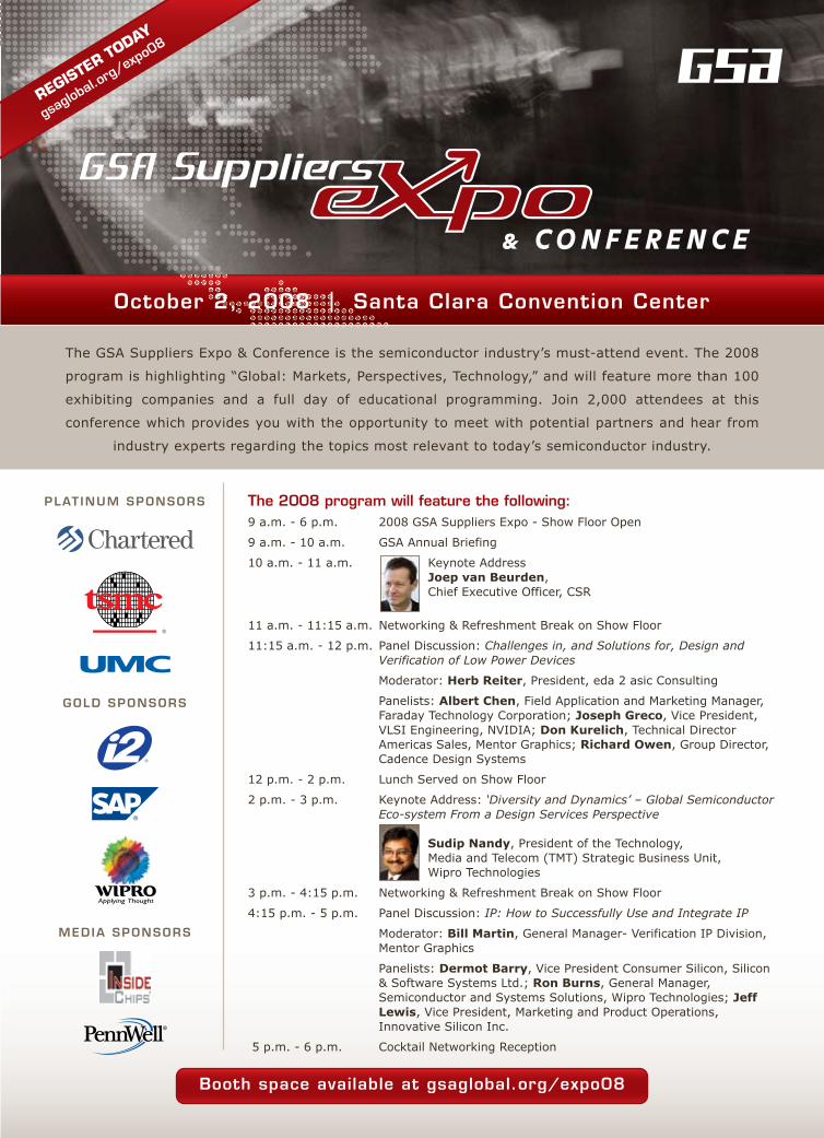
October 2, 2008 | Santa Clara Convention Center
The GSA Suppliers Expo & Conference is the semiconductor industry’s must-attend event. The 2008
program is highlighting “Global: Markets, Perspectives, Technology,” and will feature more than 100
exhibiting companies and a full day of educational programming. Join 2,000 attendees at this
conference which provides you with the opportunity to meet with potential partners and hear from
industry experts regarding the topics most relevant to today’s semiconductor industry.
The 2008 program will feature the following:9 a.m. - 6 p.m. 2008 GSA Suppliers Expo - Show Floor Open
9 a.m. - 10 a.m. GSA Annual Briefing
10 a.m. - 11 a.m. Keynote Address Joep van Beurden,Chief Executive Officer, CSR
11 a.m. - 11:15 a.m. Networking & Refreshment Break on Show Floor
11:15 a.m. - 12 p.m. Panel Discussion: Challenges in, and Solutions for, Design and Verification of Low Power Devices
Moderator: Herb Reiter, President, eda 2 asic Consulting
Panelists: Albert Chen, Field Application and Marketing Manager, Faraday Technology Corporation; Joseph Greco, Vice President, VLSI Engineering, NVIDIA; Don Kurelich, Technical Director Americas Sales, Mentor Graphics; Richard Owen, Group Director, Cadence Design Systems
12 p.m. - 2 p.m. Lunch Served on Show Floor
2 p.m. - 3 p.m. Keynote Address: ‘Diversity and Dynamics’ – Global Semiconductor Eco-system From a Design Services Perspective
Sudip Nandy, President of the Technology, Media and Telecom (TMT) Strategic Business Unit, Wipro Technologies
3 p.m. - 4:15 p.m. Networking & Refreshment Break on Show Floor
4:15 p.m. - 5 p.m. Panel Discussion: IP: How to Successfully Use and Integrate IP
Moderator: Bill Martin, General Manager- Verification IP Division, Mentor Graphics
Panelists: Dermot Barry, Vice President Consumer Silicon, Silicon & Software Systems Ltd.; Ron Burns, General Manager, Semiconductor and Systems Solutions, Wipro Technologies; JeffLewis, Vice President, Marketing and Product Operations, Innovative Silicon Inc.
5 p.m. - 6 p.m. Cocktail Networking Reception
REGISTER TO
DAY
gsaglo
bal.or
g/exp
o08

T he research accomplishments of the DARPA Center on Nanoscale Sci-ence and Technology for Integrated Micro/Nano-Electromechanical Transducers (iMINT), in its short
history of less than two years, are impressive. Under the guidance of Center Director, Dr. Y. C. Lee, and DARPA Program Manager, Dr. Dennis Polla, the iMINT Center draws on resources from a number of contributing entities: the University of Colorado-Boulder, Columbia University, the University of Texas-Austin, and Northwestern University; industry sponsors General Electric Global Research, Ibiden USA, Lockheed Martin, Ricoh Innova-tion, and wiSpry; and the National Institute for Standards and Technologies (NIST). Research-ers at this research center, based at the Univer-sity of Colorado at Boulder, have established nanowire (NW) spectroscopy as a vital tool to design defect-free/strain-free Galium Nitride NW laser components, light emitting diodes, and detectors. iMINT researchers are the only ones in the US who can grow defect-free GaN nanowires on silicon substrates. They have demonstrated the feasibility of a mass sen-sor with an atto-gram resolution operating at room temperature by using a defect-free GaN nanowire-based resonator with a quality factor Q greater than 35,000 at 2MHz. And they have demonstrated five times enhancement of the mechanical robustness of atomic layer deposi-tion-based barrier coatings. The potential outcomes based on these findings are even more impressive – the stuff of science fiction. Material so strong that it would take the weight of a two-ton car to puncture a sheet merely as thick as ordinary plastic food wrap. A card, as thin as a credit card, with the thermal conductivity 100 times better than copper. Skeptics of these futuristic
claims sarcastically say, “Right, and I’d like to sell you an interest in a perpetual motion machine.” The first description above is of a sheet of graphene, tested by Jim Hone’s DARPA iMINT group at Columbia University. Results of their study have recently been published in Science. Graphene proves to be the stron-gest material ever measured. Hone’s research required the development of atomic force microscope (AFM) tips that were durable enough to apply force capable of breaking graphene sheets. The second description is of the flexible thermal ground plane, subject of a research project headed by iMINT Center director Y.C. Lee at CU-Boulder. This single project under the guise of Program Man-ager Dr. Tom Kenny is generously funded by DARPA (the Defense Advanced Research Projects Agency). “Flexible thermal ground planes have 100 times better thermal con-ductivity than copper and will enable a new generation of high-performance, integrated microelectronic, photonic, or microwave sys-tems operating at high power density without constraints resulting from complex thermal management solutions,” according to Lee. These groundbreaking discoveries and ini-tiatives are the results of fundamental research performed by researchers at the iMINT Cen-ter, headquartered at CU-Boulder. One of eleven DARPA Nano- & Micro ElectroMe-chanical Systems Science & Technology Fun-damentals Centers, the iMINT Center is on the cutting edge of fundamental and advanced research in nano- and microsystems, nano-tubes, nanowires, and graphene. Fundamental research in engineering and applied science is the mechanism by which investigating, find-ing out, discovering, and knowing can change the possibilities of what can be created. And
advanced research turns the possibilities into reality, no longer the stuff of science fiction. Military and commercial applications will increasingly benefit from the use of microelec-tromechanical systems (MEMS), especially when anticipated significant improvements in performance are realized via the integration of microelectromechanical systems with novel nanoelectromechanical systems (NEMS). Dr. Lee relates these potential advancements to his role as director of the center and as a professor of Mechanical Engineering: “Nano-technology is the technology driver in the 21st century. Students must know more about how to integrate nano devices with micro devices. At the iMINT Center, students engage in such integration issues with hands-on, cutting-edge research experiences.” The Center draws researchers from a range of backgrounds in order to perform research that integrates micro and nano technologies. Graduate Research Assistant and National Science Foundation Graduate Research Fel-low, Joe Brown, came to the CU iMINT Center from private industry. The company he worked for in New Hampshire manufactures carbon nanotubes for use in macroscale mate-rials, using bulk quantities of nanotubes in actual electrical and mechanical applications. For example, they are developing macroscale nanotube wires that are at least as strong and conductive as copper, but at greatly reduced mass. Brown says, “Here at the University of Colorado, I’m designing microscale tools that enable nanotechnology research and develop-ment.” Research into nanotechnologies is not only aimed at making things small. “In order to access the behaviors in nanoscale devices, attention has to be paid at every level to scale – from the nano to the micro and from the micro to the macro. Nanoscale engineering requires designing at a range of size scales, not just the smallest scales.” Brown’s research aims to help other researchers to integrate nanomateri-als into active devices. It’s no longer a world of the single inventor. In the current active research environment, the new knowledge discovered and reported by one researcher is applied to new designs and new inventions by others. Collaborators within the iMINT Center plan to use Brown’s microdevices for optomechanical and electromechanical char-acterization of nanofibers, with the intent of using this knowledge in development of new sensors and other devices. Brown says, “I’m working with individual materials – one tube or one wire.” What he sees himself doing is “expanding the toolkit of what you can design with at the sub-micron scale and how things can be made at that scale.” Why is this kind of research impor-tant? “If something is small that means it’s cheap, and if it’s cheap it can be everywhere. Whether it’s a tool to build nanoscale devices
8 MEPTEC Report / Q3 2008 www.meptec.org
MEPTEC University News
University of Colorado – iMINT Center
Herbst Plaza, outside the Discovery Learning Center, home of the iMINT Center.

or a smaller microchip for a smoke detector, smaller things consume fewer resources, by reducing material consumption and energy consumption, leading to more efficient use of resources to meet the needs of real people.” Graduate Research Assistant Yadong Zhang’s research also contributes to building an effective toolkit. Zhang, who worked in the semiconductor industry in China before com-ing to CU-Boulder, is developing defect visu-alization techniques to be applied to nanoscale barrier coatings. He has developed techniques using electroplating decoration and fluores-cent tagging to quickly test the quality and reliability of barrier coatings. His approaches to inspecting surfaces test defect size and defect density and lead to higher quality, near-ly defect-free coatings. “This is the nanoscale characterization technique to help researchers know the quality of their nanoscale coatings.” As an example of useful nanoscale coating techniques, atomic layer deposition (ALD) is known for growing densely-packed, virtually pinhole-free conformal coatings. Now, ALD’s contribution to the study of nanotechnologies and barrier coatings is obvious. Y.C. Lee has pointed out that the knowledge derived from using Zhang’s approach to evaluating the quality of ALD barrier coatings on the Ther-mal Ground Plane project has led the ALD researchers to a 6000 times improvement in the quality of the hermetic sealing capabilities of their coatings. Zhang’s tests show research-ers, he says, “There is a crack; there is a defect. Good area – bad area. It’s obvious.” By virtue of this knowledge, they know which ALD coating techniques are better and which sub-strates provide better platforms for instance. Before using Zhang’s defect visualization technique, it had been hit and miss. Speaking of the quality of ALD coatings, Zhang says, “If you want to improve it, you have to know what the quality is – what’s the defect source? Where is the defect? How was it generated?” Knowing this, researchers can work towards improving the quality and reliability of their coatings. Something that makes his research important is that it saves time and increases the reliability and repeatability of the research findings. “It’s important to have a variety of defect visualization techniques,” Zhang says. His fluorescent tagging approach is applicable to ALD coatings of polymer substrates. In apply-ing this aspect of Zhang’s techniques, iMINT researchers from Mechanical Engineering and from CU’s Department of Chemistry have teamed up with industry researchers from Invitrogen. Invitrogen contributes to the col-laboration their fluorescent tag, having already been in general use in biotechnology, in hopes of finding new applications of their product. Zhang’s electroplating decoration technique applies to ALD nanoscale coatings of con-ductive substrates, such as those necessary for several research projects going on at the
iMINT Center. On this project, University of Colorado researchers from the departments of Chemistry and Mechanical Engineering are teaming up with long-time industrial partner Lockheed Martin. Prospects for more research breakthroughs are plentiful. Unprecedentedly, four mem-bers of the CU Department of Mechani-cal Engineering won DARPA MTO Young Faculty Awards in 2008 – Wei Tan for her Highly Selective, Stable and Manufacturable Nano-Bio-Sensor research, Harold Park for his research into Novel Multiscale CAE Tools for Surface-Dominated NEMS, Ronggui Yang for Surface-Plasmon Enabled High Efficiency Thermoelectric Devices, and in-coming CU faculty member Scott Bunch for his Graphene Membrane research. Dr. Bunch is the newest member of CU’s Mechanical Engineering faculty, fresh from his doctoral studies in physics and short post-doctoral assignment at Cornell Univer-sity where his research focused on graphene. “Basically, we made the world’s thinnest bal-loon.” Lots of graphene research has focused on the material’s electrical properties, but, like Jim Hone at Columbia, Bunch’s efforts have focused on graphene’s mechanical prop-erties. The carbon-carbon bonds like those of diamonds make graphene, single layers of graphite, incredibly stiff and absolutely fascinating to researchers. Making a balloon from graphene tells us that it is impermeable and opens up the study of its mechanical properties, such as its elastic modulus and its breaking strength. “You can push on graphene membranes with an AFM tip or you can inflate these membranes to make graphene balloons. In both cases, you apply controlled forces that allow you to learn about the mechanical properties of this remarkable material. The two techniques complement each other.” “Now, we’re going to poke holes in it, basically pop the balloons, see what goes through them.” Bunch asserts that with gra-phene having the best thermal and electrical conductivity and the best mechanical proper-ties of any substance ever tested, there have to be some important applications. Directions for future research include finding methods of fabrication for these yet undiscovered applica-tions. The foundations for further advanced research are firmly in place. The potential for turning more science fiction into science fact grows with each iMINT Center project. Researchers at the Center have also earned a DARPA MTO seed grant for a study to demonstrate the feasibility of a novel GaN NW-based light emitting diode with extremely high efficiency and low thermal resistance. Based on the findings from the first two years of research at the Center and the possibilities that will grow from those findings, we can say that the future burns brightly. For more infor-mation visit http://imintcenter.org/. ◆
1 - Defect morphology of ALD alumina on a copper substrate demonstrated using electroplating decoration. 2 - “Mechanical channel cracks” on ALD alumina on a polymer substrate visualized using fluorescent tags. 3 - Graphene membrane schematic. 4 - Zoom in of graphene membrane schematic.
www.meptec.org Q3 2008 / MEPTEC Report 9
n2
n4
n3
n1
University of Colorado – iMINT Center

MEPTEC Member Company Profile
Silicon Valley’s Packaging Foundry
10 MEPTEC Report / Q3 2008 www.meptec.org
P romex Industries has been a Silicon Valley microelectronics manufacturing services provider for over thirty years. Originally focused upon providing engi-
neering build prototyping services to the local Silicon Valley community, Promex has outgrown those humble beginnings to become a full service IC Assembly & Cus-tom Chip Packaging Foundry serving a world-wide customer base. What makes Promex unique is its ability to enable their customers to take new prod-ucts to market faster than by any other route. Promex has an impressive skill set of tech-nical capabilities that gives their customers “one-stop shopping” for traditional chip assembly or custom IC packaging design, development and assembly. For those customers that Promex is able to serve, Promex will “go the extra mile” and leave “no stone unturned” to help these customers take products to market quickly.
IC Assembly Services, Custom Package Development & Assembly Promex’s customer base includes the major multi-national semiconductor com-panies, fab-less semiconductor houses, high tech start-ups and emerging high tech companies. This growing customer base is attracted by their ability to lever-age Promex’s resources for a rapid, cost effective new product launch coupled with agile, scalable production. End-use markets include both commercial and military elec-tronics as well as, RF, bio-tech, bio-metric, PV solar and optoelectronics products. Promex is seeing rapidly growing demand for MEMS & MOEMS packag-ing and has pioneered stacked die and thin molded modules, especially over molded QFN configurations. The company provides IC assembly in open cavity plastic or ceramic packages, sealed ceramic packages and over-molded plastic with less than 24 hour quick turns or stepped premium deliveries of one, two or three days. No-premium standard lead time is 4 to 5 working days. On-shore pre-Asia volume production of various lead frame based packages as well as custom package and module assembly are readily available.
Much More Than Quick Turns “Several U.S. based companies provide quick turn IC assembly services which are certainly a key area of our business.” states Richard Otte, CEO and President of Promex Industries since 1995, “However… we con-sider our materials expertise a distinctive core competency. Promex extends itself further to the many customers seeking mate-rials-centric custom package development coupled with follow-on production. We offer these customers a reliable partner with the depth to develop and process engineer custom packages for high first pass yield
in production. We have capacity to scale from initial prototypes through medium production volume. This applies to tra-ditional IC assembly as well as the more complex custom packages utilizing mixed process and material sets such as are found in SiPs and MEMs products.” Responsive On Shore Assembly Otte further remarks “We have noticed two recent trends in the IC Assembly and Packaging market. First, some Asian assem-blers appear to have imposed higher mini-mum order volumes over the past few years.
Promex is experienced with stacked die, thin-molded and SiP QFN’s.
Promex is located in the heart of Silicon Valley.

As a result, some companies, especially small firms and startups that do not have high volume needs, are having difficulties finding a reliable production partner in Asia to meet their needs. Secondly, the true total cost of doing business with Asia is being recognized by non-Asian companies. The hidden costs such as freight, increased inventory carrying cost, engineering sup-port, communications difficulties etc, have CFO’s concerned. For stable commercial high volume, it usually makes sense to produce offshore, but there exists a volume range, we’ve coined the term “pre-Asia vol-ume” that many companies need fulfilled, but cannot find an offshore assembly partner willing to provide the needed service. That’s where Promex comes in. We act as a bridge
to help our customers cross the volume chasm.”
Broad Technical Capabilities After touring the Santa Clara, Califor-nia facility, it is easy to understand how Promex’s broad capabilities are attractive to their growing customer base. A 2,200 square feet, Class 1000 engi-neered clean room supports wafer sawing, die attach, wire bonding (Au ball, Au wedge, Al wedge, controlled loop Au ribbon for RF applications, copper wire), wafer handling, flip chip and custom package assembly. All wire bonders are fully automatic and sev-eral are dedicated for high reliability wire bonding on various lead frames. Wire bond pitches to 35 microns are possible. A plastic molding operation provides precision over-molding of the many lead frame based plastic packages as well as Promex’s rapidly expanding line of QFN and DFN packages. X-ray and laser mark-ing capabilities both reside in-house. Two SMT (pcba) lines, including a hands-free line optimized for RoHS compli-ant lead free assembly, offers precision SMT assembly of highly panelized boards as well as SiP (system-in-package) and COB (Chip-on-Board) assembly support. Components as small as 01005 are automatically and reliably placed on FR-4, Rogers material, flex or custom substrates.
IC Assembly in Plastic Packages Promex provides leaded plastic over molded packages as well as the increasingly in demand line of QFN/ DFN’s. Eutectic solder or epoxy die attach are standard. Assembly options include Commercial and MIL-STD-883. All plastic packages are either ink stamp marked or in-house laser marked if package serialization is requested. A listing of available leaded packages is shown in Table 1.
JEDEC Standard, Custom and SiP QFN’s The number of new QFN package sizes supplied by Promex increases monthly. All QFN and DFN over molded plastic pack-ages conform to either JEDEC MO-220 or MO-229. Nickel palladium gold lead frame finish is standard. Promex’s QFN and DFN packages are certified RoHS compliant. All QFN and DFN packages are saw singulated. Table 2 shows current open tooled plastic over molded QFN/ DFN package offerings. Check with Promex for new QFN package introductions.
www.meptec.org Q3 2008 / MEPTEC Report 11
Size DFN QFN Lead Thickness (mm) Leads Leads Pitch (nom. mm)
2 x 2 6, 8 0.50 0.9
3 x 3 8 0.65 0.9
3 x 3 8, 10 12, 16 0.50 0.9
3 x 3 20 0.40 0.9
4 x 3 12 0.50 0.9
4 x 4 16 0.65 0.9
4 x 4 20, 24 0.50 0.9
5 x 5 20 0.65 0.9
5 x 5 28, 32 0.50 0.9
6 x 6 40 0.50 0.9
7 x 7 48 0.50 0.9
7 x 7 56 0.40 0.9
8 x 8 52, 56 0.50 0.9
9 x 9 64 0.50 0.9
12x12 100 0.40 0.9
Promex Open Tooled QFN & DFN Over Molded Packages
Table 1.
State of the art wire bonding for QFN lead frame based packages.
2,200 sq ft of Class 1000 engineered clean room.
Package Lead Count Body Size Solder
SOIC 8, 16 (heat sink option) 0.150” Plate
14 0.150” Plate
16, 20, 24, 28 0.300” Coat
QSOP 16 (heat sink option) 0.150” Plate
SSOP 30 .3 mm Plate
MSOP 8, 10 3.0 mm Plate
TSSOP 8, 20, 28 4.4 mm Plate
PDIP 14, 16, 18, 20, 24, 28 0.300” Coat
24, 28, 40 0.600” Coat
Promex Open Tooled Plastic Over Molded Packages
Table 2.

MEPTEC Member Company Profile
12 MEPTEC Report / Q3 2008 www.meptec.org
While the demand for quick turn evalu-ation and characterization assembly builds using JEDEC QFN standard packages is strong, Promex is seeing an increasing market demand for custom QFN packages with irregular dimensions, non-standard footprints or deviations from the 0.9 mm +/- 0.1mm JEDEC standard height. Many emerging MEMS and RF applications must duplicate an existing footprint on a circuit board. The QFN concept is a flexible and cost effective method of designing and developing a custom plastic over molded package. A single or multiple package con-figuration is designed on a standard lead frame template, which fits a common mold. After die attach, wire bonding and over molding, the individual packages are saw singulated. This method eliminates expen-sive new molding tools for each unique package configuration. New JEDEC stan-dard or custom QFN/ DFN packages may be quickly adapted by Promex with assem-bled first articles shipped within a maximum of 4 to 5 weeks. The company has been assembling stacked die MEMS devices in custom QFN’s for the past 18 months and builds thin molded custom QFN packages with an overall height as low as 0.454 mm. In addition to MEMS packaging, Promex is experiencing a strong market demand for system-in-package (SiP) QFN assembly uti-lizing single, side-by-side and stacked die. Many customers see a need to place more than just the traditional single IC on the die attach pad and are searching for ways to save cost and space by integrating resistors, capacitors and often other semiconductor chips within an over-molded lead frame based QFN package. “There is particularly strong demand for QFN SiP’s in RF applications” comments Dr. Edward Binkley, the Chief Technology Officer of Promex. “The QFN packaging concept can offer better parasitics and ther-mal management than traditional leaded packages while also providing added design flexibility to save space and ultimately cost. Our in-house, integrated SMT capability allows us to provide a continuous process flow for over molded QFN and other cus-tom SiP’s. Promex does not need to out source the SMT portion of SiP assembly to this week’s low cost bidder. Continuous process control is particularly important with Military customers, not to mention any customer concerned about limiting the exposure of their IP to third parties. We believe we have a distinct advantage with continuous process flow for SiP assembly”.
Materials Centric Custom Package Development and Assembly In addition to lead frame based QFN SiP’s, Promex designs, develops and pro-
cess engineers a wide variety of custom packages and modules including 2-D, 3-D, Flip Chip and SMT SiP’s on various sub-strates including flex. Land Grid Arrays (LGA), Multi-chip modules (MCM) and custom Flip Chip packages are developed utilizing Promex’s core competencies and materials exper-tise focused upon providing high first pass production yield. The materials-centric cus-tom packaging approach can dramatically enhance new product introduction by opti-mizing first article approval as well as the follow on development cycle. “Materials-centric packaging combines material and volume process knowledge.” says Binkley. “The complexity of elec-tronic modules and custom packages are increasing dramatically while their size is shrinking. The drivers of RoHS compli-ance and miniaturization result in a need for higher processing temperatures, more complex assembly steps as well as a higher attention to thermal issues for the finished package. Reliable high yield production assembly processes are in-separately linked to packaging materials synergies.”
Quality Through Process Control Promex is ISO 9001:2000 certified by the British Standards Institute and utilizes Statistical Process Control (SPC) in all facets of assembly operations. Operator certification, detailed ISO and assembly documentation are coupled with the adopted “5S” philosophy to provide customers with the highest level of reliable, repeatable qual-ity. Quality control charts are readily vis-ible in the Operations area and monitor key assembly and machine settings. Process metrics, statistical trends and CpK values are integral components that drive pro-cess control and Quality Assurance within Promex’s Total Quality culture. A 3-D solder paste measurement system and on line x-ray are routinely used to verify first article set-up and ongoing process con-trol during product assembly. Clean room particle counts and relative humidity are monitored as well as wire bond pull strengths and molding parameters for each and every job.
Silicon Valley’s Packaging Foundry Silicon Valley based innovations have changed the way we live our daily lives, the way we work, communicate and do busi-ness. Several decades later, and for the fore-seeable future, Silicon Valley remains the center of global technology innovation. Promex Industries’ location in the heart of Silicon Valley means the company is exposed to, and must support, much of the emerging IC assembly and custom packag-ing requirements that emanate from this innovative part of the world. It’s those same Silicon Valley based business and communication innovations that allow customers from various parts of the country and the world to easily connect with Promex for their IC assembly and cus-tom packaging needs. Reliable new product introductions, engineering and developmen-tal prototypes, materials-centric packaging and “pre-Asia” on shore volume production are equally attractive to high tech compa-nies world wide, not just innovative Silicon Valley companies. Promex is a vital part of the packaging infrastructure that enables customers to take new products to market faster than by any other route. The future looks bright for the IC assem-bly and materials-centric packaging world of Promex Industries… Silicon Valley’s Packaging Foundry. For more information about Promex Industries, Silicon Valley’s Packaging Foundry, visit www.promex-ind.com or e-mail Chris Pugh, VP Sales & Marketing at [email protected]. Calls are wel-come at 408-496-0222. ◆
Fully automated lead free SMT optimized for SiP’s and COB.
IC assembly using ceramic packages.

RESERVE THOSE DATES FOR THE FIFTH ANNUAL
INTERNATIONAL WAFER-LEVEL PACKAGING CONFERENCEIf your business involves using or producing
chip-scale packages, wafer-level packages or anyform of advanced semiconductor packaging, you
should attend the International Wafer-LevelPackaging Conference in October.
Sign-up today to attend!
THE GOLD STANDARD WORLDWIDE INSEMICONDUCTOR PACKAGING EVENTS!
OCTO BER 13-16, 2008
SA
NJOSE, CALIFORNIA
The event of the year for buyers,specifiers and producers of chip-scale andwafer-level packaging equipment, materialsand services will be presented in San Jose
from Oct. 13-16, 2008.
If your business involves developing, marketing orselling any equipment, materials or services usedby the people who use advanced semiconductor
packaging, you should be exhibiting at theInternational Wafer-Level Packaging Conference.
Sign-up today to exhibit on Oct. 15-16!
Wafer-level packaging and much, much more!
SCHEDULED EVENTSCo-presented by
Oct. 13-14 Professional WorkshopsOct. 15 Keynote Dinner with
Dr. Thomas H. Di Stefano,Centipede Systems
Oct. 15-16 Tabletop Exhibits, TechnicalPresentations (two tracks),Special Panels and Poster Sessions
IWLPC TOPICSWLP Materials • 3D and Stacked Die
Manufacturing Processes • MEMSFlip-Chip Bumping • Photoresists
Polymers for WLP • ElectroplatingCSP/MoP/PoP/PiP/SiP/SoP
Screen Printing • Wire BondingThermal Management • UBM • Testing
Visit www.iwlpc.org or [email protected] for more information.
Platinum Sponsor Platinum Sponsor Gold Sponsor Gold Sponsor Gold Sponsor Gold Sponsor Silver Sponsor Book Sponsor Coffee Sponsors
IWLPC Ad for MR 6/19/08 3:29 PM Page 1

Indium Announces PromotionsCLINTON, NY – Indium Cor-poration recently announced the promotion of three indi-viduals - all based at Indium’s headquarters in Clinton, NY.
Eric Bastow has been promoted to Senior Technical Support Engineer. In his new role, Eric is responsible for sup-porting customer inquiries and traveling to customer sites to provide a higher level of prod-uct support in customer related projects. Eric joined Indium Corporation in 2001, where he started as a Lab Technician in Research and Development.
Mario Scalzo has been promoted to Senior Techni-cal Support Engineer. Mario is responsible for supporting Indium’s product lines and for advanced SMT problem solv-ing, as well as special assign-ments involving key customer-related projects, product educa-tion, and process training of new employees. Mario joined Indium Corporation in 2000. He served, most recently, as a Technical Support Engineer supporting the North America and Asia regions.
Tom Pearson has been pro-moted to the position of Inside Sales Manager for Indium’s Solder Products, Global Pro-cesses. Tom is responsible for managing the inside sales process across the Americas, Europe, and Asia. His focus is on small business, resource management, quality improve-ment, and sales of all solder products. Tom has worked at Indium Corporation for 24 years, serving most recently as Market Manager for Small Accounts. For more information about Indium visit www.indium.com.
APM Reaches Alliance Agreement with UMCHSINCHU – APM has an-nounced that it has reached an alliance agreement with leading global semiconductor foundry UMC for 8-inch MEMS wafer fab capacity. As part of this agreement, UMC and APM will collaborate to support current and future customers for the 8-inch MEMS process. UMC will provide the fab manufacturing, logistic management and any required capacity expansion. APM will bring its MEMS pro-cess technologies based on its development and manufactur-ing expertise dating back to 2001. The joint APM-UMC MEMS team has been work-ing together during the last 18 months for this development. An 8-inch MEMS prototype line has been set up in one of UMC’s fabs and will soon begin process qualification on one product.
Dr. Kurt Petersen, an indus-try pioneer and a member of APM’s Technical Advisory Board, says: “The 8-inch migra-tion path is key to the MEMS industry as it brings MEMS into the main stream CMOS lines, which offer many benefits from engineering innovation to cost. This is the tipping point for MEMS products to reach the consumer electronics mar-ketplace at affordable prices”. APM is one of the world’s leading independent MEMS foundry service providers. It is currently running 6-inch MEMS wafer processes in its twenty seven thousand square feet facility at Hsinchu Science Park of Taiwan. APM serves many global customers who are designing state-of-art MEMS sensors and actuators, such as pressure sensors, inkjet heads, inertia sensors, microphones, RF relay and optical mirror actuators. Kurt Petersen is one of the founders of SiTime. Prior to SiTime, he was co-founder, President, and CTO at Cepheid. Prior to Cepheid, he was a co-founder and VP of Technol-ogy at NovaSensor for over 10 years. Kurt was listed by Red Herring Magazine as a Top 10 Innovators of the Year. He is a member of the National Academy of Engineering and a recipient of the 2001 IEEE Simon Ramo medal.
STMicroelectronics, STATS ChipPAC and Infineon to Set New Milestone in Establishing Wafer-Level-Packaging Industry StandardGENEVA, SWITZERLAND, SINGAPORE and NEUBIB-ERG, GERMANY – STMicro-electronics, STATS ChipPAC, and Infineon Technologies AG have announced that they have signed an agreement to jointly develop the next-generation of embedded Wafer-Level Ball Grid Array (eWLB) technol-ogy, based on Infineon’s first-
generation technology, for use in manufacturing future-genera-tion semiconductor packages. ST and Infineon, two of the world’s leading semiconduc-tor makers, have joined forces with STATS ChipPAC, a leader in advanced three dimension-al (3D) packaging solutions, to fully exploit the potential of Infineon’s existing eWLB packaging technology, which has been licensed by Infineon to ST and STATS ChipPAC. The new R&D effort, for which the resulting IP will be owned by the three companies, will focus on using both sides of a reconstituted wafer to provide solutions for semiconductor de-vices with a higher integration level and a greater number of contact elements. The eWLB technology uses a combina-tion of traditional ‘front-end’ and ‘back-end’ semiconduc-tor manufacturing techniques with parallel processing of all the chips on the wafer, lead-ing to reduced manufacturing costs. This together with the increased level of integration of the silicon’s overall protec-tive package, in addition to a dramatically higher number of external contacts, means the technology can provide signifi-cant cost and size benefits for makers of cutting-edge wireless and consumer products. ST’s decision to work with Infineon to jointly develop and use this innovative technology, with its greater integration level of package size, marks an impor-tant milestone for eWLB on its way to becoming an industry standard for cost-efficient and highly integrated wafer-level packages. ST plans to use the technology in several products of its ST-NXP Wireless joint venture and in other applica-tion markets, with first samples expected by the end of 2008 and production by early 2010.
Hesse & Knipps to Introduce Wire Bonder for Solar MarketSAN JOSE, CA – Hesse & Knipps has announced that it
14 MEPTEC Report / Q3 2008 www.meptec.org
MEPTEC Industry News

will soon introduce a new wire bonder dedicated to the needs of the solar market in produc-ing CPV (concentrated photo-voltaic) cells. The new BondJet 820 CPV will offer all of the advanced features of the company’s Bondjet BJ 820 wedge bonder, in addition to an extended table travel of 900mm x 350mm and expanded X axis travel via the use of intelligent automation. The BONDJET BJ820 plat-form is an industry benchmark for wire bonding, offering the fastest wiring speed, largest work area and greatest axis accuracy available. “The bonding speed and flexibility of the 820 platform, coupled with the extended bonding area, will lend itself very well to the CPV market-place as well as other markets requiring such extended trav-els,” states Joseph S. Bubel, president of Hesse & Knipps, Inc. For more information call +1-408-436-9300, email [email protected], or visit www.hesse-knipps.com.
SUSS MicroTec Announces CB Wafer Bonders Series for Advanced MEMSWATERBURY, CT – SUSS MicroTec has announced the CB Series, semi- and fully-automated wafer bonders, for Advanced MEMS devices for the automotive and consumer markets. There are a variety of wafer level bonding methods for MEMS fabrication processes like anodic and glass frit, with the most commonly used in Advanced MEMS being eutec-tic, fusion, and metal diffusion bonding. The most challenging wafer level encapsulation and inte-gration needs for MEMS are met by the newly released CB series wafer bonders designed for metal bonding applications that require high temperature and high force. CB technology features bond force to 90kN and temperatures to 600˚C
along with precision tempera-ture and pressure control for unrivaled process uniformity. These features enable signifi-cant die size and cost reduction for MEMS devices. To meet the demanding alignment needs of advanced MEMS manufacturing SUSS MicroTec is releasing the BA200 Gen2, a high-precision alignment system, to comple-ment the CB series. For a smooth transition from the lab or low-volume production to full production recipes developed on the CB8, semi-automated wafer bonder, can easily be transferred to the CBC200, multi-chamber clus-ter tools.
STATS ChipPAC Offers Innovative USB Module for NAND Flash Memory ApplicationsSINGAPORE & UNITED STATES – STATS ChipPAC Ltd. has announced an inno-vative USB (Universal Serial Bus) module for NAND flash memory applications. STATS ChipPAC’s new USB flash drive design uti-lizes System-in-Package (SiP) and three dimensional (3D) die stacking technology to inte-grate NAND flash memory die, controller and passives onto a single packaging substrate for a cost-effective module solution. The USB module has the flexibility to accommodate multiple die configurations and can be customized for each customer or end application. Integrating all of the key com-ponents of a USB flash drive into a single package saves considerable space and allows for more effective signal rout-ing at a lower overall cost. In a typical design for a USB drive, the NAND flash memory die and controller are packaged in Thin Small Out-line Package (TSOP), Quad Flat Pack (QFP) or Ball Grid Array (BGA) packages. These packages may contain stacked dies, depending on the memo-
www.meptec.org Q4 2007 / MEPTEC Report 13
SonoLab, a division of Sonoscan®, is the world’s largest inspection service specializing in Acoustic Micro Imaging (AMI). Through SonoLab, you’ll have access to the superior image quality and reliable data accuracy of Sonoscan C-SAM® acoustic microscopes, plus the capabilities and careful analysis of the world’s leading AMI experts.
To learn more visit www.sonoscan.com/sonolab
With worldwide locations, unmatched capabilities, extensive experience and the best equipment available, SonoLab gives you the ability, flexibility and capacity you need to meet all your AMI requirements.
SonoLab™ Services
to Industry Standards
and Evaluation
and Lot Reclamation
Constructional Analysis
SonoLab is Your Lab
Surface mounted device with delamination (red) along the entire
length of several leads. This part would fail per J-STD-020 criteria.
®
™

ry density requirements of the end application. The discrete NAND flash memory and con-troller along with passives are then mounted onto a printed circuit board (PCB) using sur-face mount technology. This normally consumes most of the usable area allowed by the form factor of the USB flash drive. The innovative USB mod-ule design is the latest addi-tion to the Company’s portfo-lio of solutions for removable solid-state storage applications. STATS ChipPAC offers a vari-ety of memory card formats which utilize the most up-to-date technologies and process-es unique to memory cards, including integrated curve-cut-ting, labeling, mechanical card assembly and card packaging. In addition to assembly, STATS ChipPAC offers memory card test services with dedicated re-sources to support test develop-ment. With global headquarters in Singapore, STATS Chip-PAC has design, research and
development, manufacturing or customer support offices in 10 different countries. STATS ChipPAC is listed on the SGX-ST. Further information is avail-able at www.statschippac.com.
Pac Tech USA Announces Grand Opening Celebration for New Asian FacilitySANTA CLARA, CA – Pac Tech Packaging Technologies held a grand opening celebra-tion on September 18 at its new 55,000 square foot facility in Penang, Malaysia. In conjunc-tion with the opening celebra-tions, Pac Tech held a techni-cal symposium on September 19 at the Equatorial Hotel in Penang. The facility is located at 11900 Bayan Lepas, Byan Lepas Industrial Zone, Penang, Malaysia. Government offi-
cials, dignitaries and industry leaders were in attendance. The new facility provides state-of-the-art wafer bump-ing and backend processing for semiconductor companies within the Pacific Rim. The building has 40,000 square feet of remodeled production floor space, including cleanroom area. Both are equipped with the latest generation equipment for 300mm wafers. The new Malaysian facility
is designed and laid-out to ac-commodate mass-production, and is capable of handling up to 600,000 wafers per year. Pac Tech Asia will provide a variety of special applica-tions designed to enhance and support the Asian semiconduc-tor manufacturing community. The applications supported will include: electroless Ni/Au under-bump metallization for copper and aluminum devic-es, solder-paste stencil print-
16 MEPTEC Report / Q3 2008 www.meptec.org
MEPTEC Industry News
U.S. and Canada Representative:Please contact [email protected] or call408-588-1925
www.pactech.de
� Perfect reflow soldering� Rapid thermal annealing under
controlled atmosphere, vacuum and pressure
� Perfect solder joints, no voids
Also available PEO –Semiconductor
Process Furnaces
SRO – Solder Reflow Ovens
• Free Wireless Internet Access• 176 Spacious Guest Rooms• Full Service Restaurant• In Room Coffee Makers, Refrigerators, Hairdryers, Irons and Ironing Boards, AM/FM Clock Radios and Digital Safes• On Demand Movies• Voice Mail• Heated Outdoor Pool and Jacuzzi• Banquet/Meeting Space for 250• Japanese Tatami Rooms
• Minutes from Light Rail, Santa Clara Convention Center and Paramount’s Great America• 24 Hour San Jose Airport Transportation• Special Group Rates and Packages
S I L I C O N V A L L E Y
The only full services Ramada in Silicon Valley408-245-5330
1217 WILDWOOD AVENUE • SUNNYVALE, CA 94089

www.meptec.org Q3 2008 / MEPTEC Report 17
ing for flip-chips, solder-ball placement for wafer-level CSPs down to 200µm ball diameters, and micro solder-ball place-ment for fine-pitch applications down to 80µm. More advanced applications include: Ni/Pd/Au metalization for today’s power MOSFET devices and gold wire bonding, tall Ni/Au bumping for RFID applications. The facility offers up to 300mm wafer pro-cessing capability. The facility is now accepting process quali-fication orders. Semiconductor companies can begin to provide Pac Tech GmbH and Pac Tech USA with their wafer forecasts in order to begin allocation of time and schedule them into the production planning. Pac Tech GmbH and Pac Tech USA can also be contacted to begin the pre-qualification of processes to be used in the new Asian facil-ity. Dr. Thorsten Teutsch, Pres-ident of Pac Tech USA and Vice President of Operations for Pac Tech Asia, comments, “The new facility in Malaysia
establishes our global presence. It will also help Pac Tech USA address new customers and increase our domestic business as an entry portal for high-volume customers to our Asian facility.” More information is avail-able at www.pactech.com.
Hesse & Knipps Presents Most Flexible and Fastest Wedge Bonder for Both Ribbon and Wire BondingSAN JOSE, CA – Hesse & Knipps, leading manufacturer of high-speed, fine pitch wedge bonders for the back-end semi-conductor industry, introduced the BONDJET BJ820 during Semicon West’08. The BOND-JET BJ820 is a high-speed, fully automatic wedge bonder that offers the ultimate in flexi-
bility for both high-speed round wire and deep access ribbon and wire bonding. It handles all challenging fine pitch wire bonding applications in a sin-gle platform - including RF and microwave devices, COB, MCM and hybrids, fiber optics and automotive - using alumi-num or gold wire or ribbon. The fastest wedge bonder on
the market, BONDJET BJ820 offers bond speeds up to 7 wires/second. With axis repeatability of 1µm at a balanced encoder res-olution of 20nm, the BOND-JET BJ820 provides increased process stability that enables reliable bonding of extremely small bond pads with a larger wire diameter. A highly versa-tile 12” x 16.1” work area can serve as two or more smaller stations for efficient handling of smaller products or substrates. Coupled with intelligent auto-mation solutions, parallel bond stations in one work area can eliminate significant indexing time, resulting in 60% greater throughput than competing machines. Other significant machine capabilities include:• 12.5µm to 85µm diameter wire bonding• Ribbon bonding from 6µm x 35µm to 25µm x 250µm• Constant loop height and wire length• Maintains parallel loops with


in mixed reference system• Auto teach for linear applica- tions, reducing programming time “The BONDJET BJ820 defines the benchmark in the industry by offering the fast-est wiring speed, largest work area and greatest axis accuracy among its competition,” sum-marizes Bubel. With a footprint of only 720 x 1250mm, the BONDJET BJ820 can be easily integrated into existing floor plan configu-rations or new concepts. For more information on the BONDJET BJ820, email [email protected] or visit www.hesse-knipps.com.
Rudolph Technologies Announces Ordersfor WaferWoRx 300 Probing Process Analysis SystemsISSAQUAH, WA – Rudolph Technologies, Inc. has an-nounced the receipt of orders from a major European semi-conductor manufacturer for two WaferWoRx® 300 Probing Process Analysis Systems. The orders were placed as part of a multi-tool agreement signed in June 2008. The WaferWoRx 300 Sys-tem allows semiconductor man-ufacturers to make informed decisions based on quantifiable data about their wafer prob-ing process in order to increase yields and reduce operating costs. Rudolph’s Probe Card Test and Analysis product manager, Darren James, stated, “We are continually seeking opportuni-ties to reduce the cost and com-plexity of wafer probing and other final test processes. With today’s multi-site, multiple test probe processes, determining the root cause of yield loss is a challenge for our custom-ers. The WaferWoRx generates analyses that helps pin-point the most likely source of prob-ing process problems.” The WaferWoRx 300 is a probing process analysis system that uncovers potential process
problems and defines practical solutions based on data from individual probe tips and scrub marks, and on the detection and analysis of larger-scale patterns within the aggregated data. Using automated analysis from WaferWoRx, test engineers can
evaluate the stage accuracy, per-formance under load and test at temperature characteristics of the prober. They can prequalify test cells without risk to produc-tion wafers and evaluate the readiness of the probing pro-cess for advanced technologies
such as multi-DUT and high pin count probe cards. In addi-tion, probe card performance can be tracked to predict the need for maintenance. This step is designed to extend card life and maximize card availability while avoiding the yield losses
MEPTEC Industry News
www.meptec.org Q3 2008 / MEPTEC Report 19
� Quick-turn and mass-production
� Highly competitive, low-cost bumping technology
� Exceptional quality through high-level expertise
Available Processes� Electroless Ni/Au under-bump metallization � Ni/Au bump for ACF or NCP assembly� Solder paste stencil printing� Solder ball drop for wafer-level CSP� Solder jet for micro-ball placement� BGA and CSP reballing� Wafer backside thinning and wafer dicing
Special Features/Technologies� Over 10 years experience� U.S. Government Certified� 4- to 12-inch wafer capability� Wafer pad metallization: Al and Cu� Solder alloys: eutectic SnPb37, lead-free,
low-alpha, and AuSn� Fluxless and contactless bumping for MEMS
and optoelectronics� Ni/Au interface for wire-bond applications
The leader in low-cost electroless wafer bumping.
Pac Tech GmbHTel: +49 (0)3321/[email protected]
Pac Tech USATel: 408-588-1925, ext. [email protected]
Pac Tech Asia Sdn. Bhd.Tel: +60 (4) 6430 [email protected]
NAGASE & CO., LTD.Tel: [email protected]
Global Low-CostWafer Bumping Services
• Europe – USA – Asia •

that can occur when a card fails during use. Data generated by the Wafer-WoRx 300 can produce quanti-fiable benefits by reducing yield losses in the probing process and increase the lifetime and availability of expensive con-sumables, such as probe cards. Additional information can be found at www.rudolphtech.com.
Sonoscan Launches HiRes Generation THRU-ScanELK GROVE VILLAGE, IL – Sonoscan, Inc., has introduced
the HiRes Generation THRU-Scan™, which significantly en-hances through-transmission imaging with Sonoscan’s C-SAM® line of acoustic micro-scopes. Reflection-mode acoustic imaging (the most frequently used mode) is limited to a de-fined depth within a sample, but THRU-Scan images the whole thickness in one scan. For example, a plastic-encapsulated microcircuit might have five layers. Reflection-mode imag-ing typically selects one or two internal interfaces to image for anomalies or defects. But THRU-Scan images the whole thickness of the part – all five layers and all four interfaces
– simultaneously, and reveals a defect or anomaly at any depth. By itself, THRU-Scan provides a fast non-destructive method for determining whether an in-ternal defect is present. Often THRU-Scan is used along with reflection-mode imaging to simultaneously verify the x-y location of a defect and specify its depth. HiRes Generation THRU-Scan differs from previous versions by permitting much higher resolution in the acoustic image without sacrificing pene-tration. Edges are more sharply defined, contrast is greater, and thicker samples can be imaged. For more information, con-tact Steve Martell, manager
of technical support services, Sonoscan, Inc., 2149 E. Pratt Blvd., Elk Grove Village, IL 60007. Phone: 847-437-6400 x 240. [email protected].
SAN JOSE, CA – North America-based manufacturers of semiconductor equip-ment posted $905 million in orders in July 2008 and a book-to-bill ratio of 0.83 according to the July 2008 Book-to-Bill Report published by SEMI. A book-to-bill of 0.83 means that $83 worth of orders were received for every $100 of product billed for the month. The three-month average of worldwide bookings in July 2008 was $905 million. The bookings figure is three percent less than the final June 2008 level of $934 million, and 36 percent less than the $1.41 billion in orders posted in July 2007. The three-month average of worldwide billings in July 2008 was $1.09 billion. The billings figure is about six percent less than the final June 2008 level of $1.16 billion, and about 36 percent less than the July 2007 billings level of $1.69 billion. “Orders for semiconductor equipment continue to reflect the pronounced cut-back in capital expenditures this year and are at the lowest levels since November 2003,” said Daniel Tracy, senior direc-tor of Industry Research and Statistics at SEMI. “While chip-makers remain atten-tive to cost controls, this remains a highly cyclic industry. Factory utilization levels, unit demand growth and planned fab proj-ects suggest that new investment activity will resume in 2009.
The SEMI book-to-bill is a ratio of three-month moving average bookings to three-month moving average shipments.
Shipments and bookings figures are in millions of U.S. dollars. ◆
Bar scale starts at 255 per increment
1400
1500
1600
1700
1800
1900
2000
20 MEPTEC Report / Q3 2008 www.meptec.org
North American Semiconductor Equipment Industry Posts July 2008 Book-To-Bill Ratio of .83
Aug Sep Oct Nov Dec Jan Feb Mar Apr May Jun Jul 08
$904.8
12 Months Ending July 20082000
1500
500
0
1000
$1087.4
MEPTEC Industry News
Book-to-Bill RatioBook-to-Bill Ratio
.81 .83.78.87 .82.92.79 .80.82 .85 .89.82
Average Bookingsin Millions of Dollars
Average Shipmentsin Millions of Dollars
Previous THRU-Scan (top) sacrificed resolution for penetration. New HiRes Generation THRU-Scan (bot-tom) gives superior resolution and has better penetration.

SUSS MicroTec Unveils 300mm Mask Aligner for 3D PackagingMUNICH, GERMANY – At Semicon West 2008, SUSS MicroTec unveiled the second generation of its MA300 Pro-duction Mask Aligner featuring a dedicated alignment kit for creating 3D interconnects for applications like chip stacking and 3D image sensor packag-ing. High alignment accuracy is required to enable 3D applica-tions ranging from latest-gen-eration mobile consumer elec-tronics to supercomputers The new 3D-Alignment platform enables bottom side and infrared alignment for 300mm based three-dimension-al (3D) packaging lithography applications, thereby enabling cost effective mask aligner sys-tems to meet the most aggres-sive technology roadmaps for thick resist applications and
keep costs low relative to 1X Stepper lithography solutions. While bottom-side align-ment enables SUSS 300mm Mask Aligners to process dou-ble-sided structured wafers, the infrared alignment option allows the handling of opaque, yet IR-transparent materials such as adhesives, in particu-lar for thin wafer handling or encapsulation applications. For more information visit www.suss.com.
Seventy Fab Projects Brighten Industry Outlook in 2009SAN JOSE, CA – According to the World Fab Forecast report, recently released by SEMI, a projected decline in world semi-conductor fab equipment spend-ing of 20 percent is expected for 2008, but a rebound of over 20 percent in spending is expected in 2009, driven by over seventy fab projects. The August 2008 edition of the report lists 53 fab
equipping projects and up to 21 construction projects for fabs in 2009. In 2008, 300mm projects make up about 90 percent of all fabs equipment spending, while about 69 percent of all equip-ment spending is for 65 nm and below technology nodes. Over-all annual semiconductor fab capacity in 2008 is expected to be about 16 million wafers (in 200mm equivalents), a growth rate of just nine percent com-pared to 17 percent capacity growth in 2007. In 2009, capacity is expect-ed to grow about 10 percent. Memory makes up the larg-est share of total semiconductor fab capacity with a 40 per-cent share in 2008, followed by foundries with over 20 per-cent, and logic with 15 percent. In 2009, memory will slightly increase its share to 42 percent, while foundries and logic are forecasted to remain at about the same share levels. There have been dramatic changes in spending on fab
construction projects. Many projects have been delayed during 2008 (with a decline in construction spend-ing of 38 percent from 2007), but 2009 will show over 50 percent growth in construction spending when many of the pushed out projects begin. Over most of the past decade, Japan has spent the largest share of money on fabs equipping. This will change in 2009 with Taiwan and S. Korea exceeding Japan in fab equipment and construction spending. By 2009, the share in total spending throughout the Asia Pacific region (excluding Japan) will rise to over 67 per-cent (from 50 percent in 2006). In 2008, only four semiconduc-tor companies spent over $1.5 billion. In 2009, the World Fab Forecast predicts twice as many will spend at that level. For more information on SEMI’s World Fab Forecast reports visit the SEMI website at www.semi.org/fabs. ◆
www.meptec.org Q3 2008 / MEPTEC Report 21

T oday’s processors are becom-ing increasingly complex con-sisting of many different I/O standards such as PCIe Gen2, DDR3, XAUI, RGMII, etc,
with each block likely from a different IP provider. Each IP block may come as a hard macro with a unique bump arrangement, or pad arrangement in case of wirebond, for signal, power, and ground, they also can each have a unique bump pitch, and may have sev-eral different power and ground. Ideally, the IP provider should provide package integration guidelines, but these guide-lines may not be practical for the end-user as they are typically written as best design practices with no consideration for the conflicting requirements of the various other IP or cost considerations of the design. It is up to the end user to confirm that the electrical require-ments of the IP or standard are being met and the only way to ensure this is by performing signal integrity analy-sis as part of the design and planning process for both pre- and post-layout. The challenges of designing a first pass working package start long before the die is complete, and in order to ensure a solid design in which all of the electrical requirements are to be met the package must be designed with a sound founda-tion (Figure 1). The most critical phases of the design are during the Package Technol-ogy Selection and Bump/Ball definition stages. The first consideration are what types of interfaces are required, where are they floor-planned on the die, and how the balls will be assigned to match their relative positions in the system. Without proper floor-planning the result can be poor power-integrity due to sub-optimal signal via placement or signal crossings/jumpers in the design. The bump arrangement drives the stackup assignment of power/ground/signal lay-ers and if the bump assignment is not done properly it can lead to increased layer count requirement, higher cost,
and poor performance. An example of stackup/bump co-design (Figure 2) may have power/ground referenced microstrip for all signals, and decou-pling capacitors may be desirable. If the outer row of bumps are assigned ground, then the natural selection for top package layer is ground. If the second layer is to be signal, the next ring(s) of bumps should be signal bumps and in the case of multiple signal rings, they should have sufficient pitch and small enough pad size to ensure that inner bumps targeted for the same layer can breakout. For high-performance designs power-integrity design and analysis is vital. It has been the author’s experience that
most package failures are a direct result of power-integrity issues related to either the core-supply or the I/O interface supplies. Generally speaking, package power-integrity failures cannot be solved at the board level and require either a respin of the die or the package (or both) in order to meet target spec for operating frequency and voltage. Of course, increasing the supply voltage may remedy the problem at cost of high-er power, but if this is not an option then respin of the die/package is necessary. As described earlier, the bumps drive the stackup and if later it is determined that on-package capacitors are required, the bumps will not be optimum for package capacitor hookup, limiting the number of possible capacitor component place-ment locations if signal routing is on the top layer of the package, and insufficient plane distribution which is required to ensure low impedance connection be-tween ground and power supply from the cap to the die. In general it will be simpler to connect capacitors between I/O power and ground than it is between core power and ground. Other practical limitations for substrate capacitor place-ment are dictated by assembly rules due to spacing requirements between sub-strate capacitor and die edge to allow for underfill bleed out (Figure 3). Addition-ally there is component size and spacing to the lid/stiffener, if one is present, to
22 MEPTEC Report / Q3 2008 www.meptec.org
MEPTEC Package Design
Fundamental Challenges in High-Performance Package DesignDaniel Lambalot, Director of Engineering Bayside Design, Inc.
Figure 1. Building blocks for a well designed package.
Figure 2. Optimum die bump to plane layer breakout.

avoid assembly issue and/or short-cir-cuits. For these reasons the substrate body size needs to be sufficiently larger than the die to allow for capacitors on some or all sides. Of course, the best place for capacitance is on the die, how-ever IC design teams struggle to this day with accurate prediction of total on-die capacitance from the various sources of not just explicit decap, but also parasitic metal and junction/side-wall capaci-tance; therefore it is sometimes safe to plan for substrate caps in advance. The separation from die-edge to capacitor builds in a physical separation which results in a mounting inductance, in addition to the high intrinsic induc-tance of the capacitor itself making it less effective than on-die cap. A well designed stackup can have a low mount-ing-inductance of anywhere from 80pH for the package capacitor nearest the die and as high as 175pH for large body package capacitor placed furthest from die. Despite the lower effectiveness of substrate capacitors vs on-die cap, they may still be desirable if one considers that either during test/characterization
or perhaps in actual system there will be a socket which will add significant height, and therefore inductance, to the package. Core supply power balls as well as ground balls are typically restricted to the region directly under the die core, sometimes referred to as the die-shadow. The assignment of power vs. ground is often arranged in a checker-board pattern for high-performance flip-chip devices which maximizes coupling between power and ground balls and vias thus resulting in lower inductance and typically better performance. Having laid the foundation for power-integrity and clean breakout, to ensure signal integrity the traces for each inter-face should be the correct width to achieve the desired impedance target for the interface. As feature sizes shrink it is increasingly difficult to control imped-ance in the package. Driving factors for impedance are more than just reduc-ing signal reflections but also standards compliance. More and more SerDes standards are ratified with return-loss specifications and these must be met in order to claim compliance. Return-loss is a Microwave/RF term which in early times was literally defined as the round-trip (return) power loss of a cable or other waveguiding structure with a short-circuit at the end. In recent years it has become more synonymous with source or load impedance match-ing quality. A 100-ohm differential pair in a package is typically specified to be 100ohm +/- 10%. XAUI, a popular standard for 10Gb ethernet backplane applications has a frequency dependent return-loss mask (Figure 5). It is seen that at +/-10% impedance mismatch
from nominal, the return-loss is already -20dB leaving only 10dB margin for receiver return-loss compliance. At +/-20% matching tolerance there is a mere 6.8dB margin - a loss of over 7dB dynamic range. Considering pro-cess variation of 65nm and soon 45nm SerDes and capacitance of on-die ESD structures it is extremely challenging to design such that the assembled die/pack-age meets the letter of the standard. Once the design is complete and meets signal integrity requirement ad-ditional time is required time to go through CAM checks and vendor spe-cific design for manufacturing checks to help improve yield. Substrate indus-try lead times change from quarter to quarter, and in recent months at time of this publication substrate lead times for HDBU organic substrates have become comparable to that of the die fabrication process. This means that for the substrate to be available when the silicon is back from fab for assembly, any required sig-nal integrity analysis and design checks should ideally be completed several weeks before final tapeout of the die. Signal-integrity analysis requires sufficient information about the sys-tem while designing the package. The amount of switching noise will depend on the PCB loading of the I/O, the I/O strength and edge-rates, and amount of available on-die decap. As edge-rates increase, noise and crosstalk will increase. Configurable I/Os can eas-ily have settings which will exceed the capabilities of the package, particularly in wirebond designs. The performance limits of the package should be deter-mined to restrict operating beyond the
www.meptec.org Q3 2008 / MEPTEC Report 23
Figure 4. Restricted component placement due to dense trace routing on top layer.
Figure 3. Substrate capacitor placement feasibility and keepout restrictions.
Figure 5. XAUI Return-Loss Compliance Mask vs. Impedance Tolerance.

capabilities of the substrate which will reduce customer support/debug later. Before analysis can be started appro-priate models must be extracted from the post-layout data (Figure 6). The model format is dependent on whether it contains coupled signals and power/ground, if it is just for core-supply network, or if it is coupled differential pairs for crosstalk and serial interface analysis. Ultimately the signal integrity engineer will depend on electromagnet-ic field solvers to most accurately model the package using post-layout design data. To keep the design cycle moving along, the layout can be partitioned into phases such that core-supply or another interface is routed either partially or to completion so that model extraction and analysis can start. While the analysis of the first interface is being performed the
layout of the second interface can be designed, and layout and analysis can proceed in lock-step fashion. This ensures quick completion of layout and signal integrity activities and if both lay-out and signal integrity activities are in-house an efficient and effective means to deliver signal integrity driven layout. Another important design consider-ation is if the package will be used in a socket in which case the socket should be included as part of the design, model-ing, and analysis of the package. Even if the end-user application does not require a socket, the part will ultimately need to be tested and a pogo-pin socket may be the interposer between the assembled die/package and the board. Sockets are typically several millimeters thick and this is several times thicker than the package resulting in several times more
inductance. If the part is required to test at speed for whatever reason, it may well experience failures in this environ-ment. For this reason careful attention should be paid to signal to return-ratio (the number of signal balls divided by the number of power/ground pairs) as well as the proximity/placement of power/ground relative to signals. Eventually parts will come back from fab and it must be determined whether the modeling methodology correctly predicted the actual performance or not. It is not enough that the part works, but does it work for the right reasons? Are the impedances being met, and if not is it due to the tools, the material information or finished trace widths and dielectric thicknesses? It is an extremely complicated process to go from physical design to broadband models which are accurate across a broad range of fre-quencies, and most EDA vendors do not have lab equipment and test structures to correlate their tools to measurement and rely on their customers to provide this feedback. For this reason it is important for any design team to perform correla-tion of actual hardware with modeling as it is essential to develop a robust design flow, and to do it properly is expensive. The equipment required is substantial in cost as well as complexity and the required skill set to do it accurately is rare. Essential to a package character-ization lab is a microwave probe sta-tion with optics that allow for probing features as small as 50µm-250µm pitch, adjustable micromanipulators, calibra-tion standards, high-speed oscilloscope with TDR (Time-Domain-Reflectom-etry) generators to measure impedance and delay of single-ended and differ-ential signals, and microwave vector network analyzer for measurement of supply impedance, return-loss/insertion-loss, and dielectric information such as permittivity and losses. ◆
Daniel Lambalot is Director of Engineering at Bayside Design, a high-speed design services company situated in Silicon Valley, with hundreds of high-performance package and board designs. Daniel holds an MSEE from the University of Illinois at Urbana-Champaign. His experience includes full-custom CMOS design for high-speed I/O and die-architecture modeling while at Com-paq Computer (Digital Equipment Corporation) as well as signal integrity for package/board design.
24 MEPTEC Report / Q3 2008 www.meptec.org
MEPTEC Package Design
Figure 6. Translation from complex 3D structure to lumped R,L,C,G or S-Parameters.
Figure 7. Characterization lab. (Bayside Design)

“I found a new supplier whose product will save us thousands of dollars a year.”
Barry BorwegeSPX Service Solutions
Owatonna, MN
Mandalay Bay Resort & Convention CenterLas Vegas, Nevada
Conference & ExhibitionMarch 31–April 2, 2009
MeetingsMarch 29–April 2, 2009
PCB and Electronics Assembly Trade ShowSolve your manufacturing challenges, visit hundreds of exhibitors and meet thousands of peers and industry experts in board design and manufacture, electronics assembly, and test. Take advantage of 60+ full- and half-day courses and IPC standards meetings. Focus on advanced technologies, environmental regulations, materials and SMT processes. Pre-register for free exhibit hall admission and take advantage of free keynotes, posters and forums.
www.IPCAPEXEXPO.org

A ccording to Gordon Moore, Intel founder, CEO and cre-ator of Moore’s Law, the physical limits of his “law” are rapidly approaching.
When asked about it recently, he stated that “we’re approaching the size of atoms which is a fundamental barrier.” The spir-it and successes generated by an Industry focusing on Moore’s law will hopefully continue using modified definitions of the law to maintain the pace of innova-tion and improvement. One way this is accomplished is to build more capable “systems” whether they are built from multiple chips bonded in a System in a Package (SiP) or chips/wafers bonded in a stack using 3D interconnect/thru via technology. Either of these processes will demand that the die to be mated are KGD (Known Good Die) prior to whatever scheme is used. Failure of any die in the stack renders the entire stack or package useless. Because MEMS devices many times require a control ASIC or are a part of a more complete complex system, these new packaging schemes will rapidly grow in volume. Supplying KGD to the final assembly will reduce costs, reduce system size, and shorten time to market. There are several reasons that make supplying MEMS KGD important. The rise in use and acceptance of SiP, multi-chip modules, and expensive packaging schemes dictate that the lowest possible cost to manufacture the final device will come as a result of 100% working die. Previously, KGD were primarily desig-nated statistically. While this can indicate a very high percentage of good die, it is not capable of guaranteeing that every chip put into the packaging process start-ed as a fully functional chip. Traditional wafer level test of full wafers allows the test engineer to deter-mine that the chip is fully functional prior to the singulation process. With newer methods of singulation rapidly replacing the older processes, the loss of die at singulation has dropped. However, with up to 70% of the final cost of
the MEMS product in the packaging process, the packaging of even a small number of “bad” die can increase the total cost of production significantly. This is especially true for devices mounted in extremely expensive packages such as some IR sensors which are mounted in very expensive vacuum dewers.
MEMS devices, however, present a more challenging problem due to the need for many of these devices to be packaged in a specific environment (such as vacuum), simulated by an outside non-electrical source (sound, temperature, vibration, motion, etc.) and the unique non-electrical measurements that must be taken to measure proper operation of the DUT(motion, light, etc.). These same requirements also make the device more susceptible to damage in the singulation process. Small structures can be dam-aged by the singulation process itself or from minute debris that contaminates the device during the process. Testing singulated die on stretch frame has been possible for many years. With the ability of pattern recognition sys-tems, the “new” position of the DUT after stretch could be determined and the device positioned for test. However, these systems required an interim step between die to allow the pattern recogni-tion system to find the device and make the corrections required. This was and is a time consuming process increasing the time and cost of test and making such schemes many times unpractical. A new system offered by SemiProbe, a provider of manual semi and fully automatic prob-ing systems, utilizes a unique EVA system to scan fields of die at high speed and then using these images “learns” the X,Y, theta and Z position of each individual die after stretch. The prober is then able to step at normal speeds making high speed, high thruput, and cost effective testing pos-sible. Because the scanning process is automatic and away from the test prob-ing field, the area above and around the DUT is available for special stimulation or measurement instruments. EVA has proved to provide an additional benefit. Traditional test sys-tems have not been able to take bro-ken wafers and fragments and test them efficiently. With EVA, a fragment is auto scanned, a wafer map automati-cally drawn, and the fragment is probed without operator intervention. All test
26 MEPTEC Report / Q3 2008 www.meptec.org
MEPTEC KGD Testing for MEMS
Why 3D Interconnect and New SiP Packaging Schemes are Demanding KGD for MEMS DevicesDon FeuersteinSemiProbe
KGD Test Sequence.

data is exported in a standard wafer map format. After a device failure, the ability to do failure analysis to determine the root cause is difficult due to the destructive nature of the process to delaminate the layers. While a variety of new test pro-cesses can help the test engineer deter-mine where the failure is, they are time consuming and a “wrong” guess as to the layer where the failure is occurring will render the sample useless for fur-ther analysis. By supplying KGD to this “package,” the test engineer can greatly reduce the prospect of system failure as a result of this chip. KGD has proved to be a smart busi-ness decision as Macronix (a memory producer) increased revenues by 12 per-cent, despite an increase in price pressure, while the gross profit jumped an impres-sive 39 percent as compared with the same time period last year after moving to KGD! 1 For MEMS companies, the “mating” of their die with a control ASIC and/or other device used to create a com-plete system makes KGD essential. KGD can be accomplished at costs comparable to full wafer test, and the added benefit of salvaging broken wafers, removing critical alignment from operator respon-sibility and your choice of semi or fully automatic systems based upon wafer test times make financial sense for you and your customers. For more information please visit www.semiprobe.com or email Don Feuer-stein at [email protected]. ◆
1 Industry News – Memory Semiconductor Electron-ics, “Macronix offers KGD chips”, Thursday, August 02, 2007, CST Inc., 2336 Lu Field Road, Dallas, Texas 75229, www.simmtester.com, Tel: +1 (972) 241.2662.
www.meptec.org Q3 2008 / MEPTEC Report 27
SemiProbe SA-8 EVA.
MEPTEC Special Report
L ast year Bette Cooper of MEPTEC was contacted by a Department of Labor contrac-tor asking to assist the D.O.L. in creating job descriptions
and identifying professional training resources associated with the MEMS and microelectronics industry. Several MEPTEC advisory board members responded, providing a variety of tech-nical inputs, resulting in up-to-date information and resources. This input has resulted in new official govern-ment text describing this industry and its practitioners, now appearing in sev-eral D.O.L. documents, notably. The project leader, Ms. Christy Kroustalis, of Research Triangle Institute, RTI, has acknowledged our help. In December of 2007, Bette was contacted by Ron Wandscher of RTI in North Carolina, retained by the US D.O.L, to update the O*NET Data-base. To paraphrase their request: O*NET stands for Occupational Infor-mation Network and is a database accessible by the public via the inter-net (at no cost, which provides infor-mation about the skills, tasks, work context, and knowledge requirements of 900+ occupations in the United States. http://www.onetcenter.org/) It replaces the 70-year old Dictionary of Occupational Titles as the nation’s primary source of occupational infor-mation. The U.S. Department of Labor believes the maintenance of this data-base plays an integral role in assuring the vitality of the American economy. More information about this program is available at the U.S. Department of Labor’s website at http://www.doleta.gov/programs/onet/.
Ron contacted MEPTEC, as a leading microelectronics trade orga-nization, to identify experts in the field, and to provide needed facts and contacts to help RTI. Their objective is to incorporate this emerging and increasingly important profession into the governments database of technical industries. Bette sent out a heads-up to several MEPTEC Advisory Board and members. Response (by Phil Marcoux, Joe Fjelstad, Rich Rice, Jeff Braden, Dhiraj Bora, and many others) was immediate and gratifying, resulting in suggestions on resources and identifi-cation of experts in the field. Tom Clif-ford provided overview summaries and graphics as well as coordination of responses, suggested revisions to their document #17-22199.06, conference reports, and suggested job descrip-tions. Ms. Kroustalis offers her appre-ciation to all of MEPTECs efforts: “The information you provided us was very valuable. We took your informa-tion and incorporated it into O*NETs formatting for task development and descriptions. We believe the end result is a more defined, well-rounded description of MEMS and Microelec-tronic engineers. We very much appre-ciate all the work you have done with the revisions to our Microelectonics Engineer profile”. MEPTEC welcomes the opportu-nity to assist government efforts to support our domestic microelectronics industry and profession. For the D.O.L. “Microsystems Engi-neers” task list summary and descrip-tion please contact Bette Cooper at [email protected]. ◆
MEPTEC Assists U.S. Department Of Labor:Provides Job Descriptions and Skill-Sets for MEMS and MicroElectronics Professions
Tom CliffordMEPTEC Advisory Board
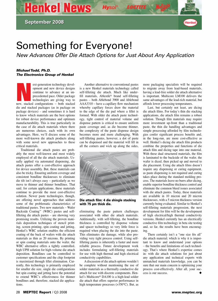
N ext-generation technology devel-opment and new device designs continue to advance at an un-precedented pace. Older package technologies are giving way to
new, stacked configurations – both stacked die and stacked packages (as in package on package devices) – and sometimes it is hard to know which materials are the best options for robust device performance and optimum manufacturability. This is true particularly in the case of die attach materials where there are numerous choices, each with its own advantages. Here, we’ll discuss some of the more well-known die attach products along with some novel new approaches to these critical materials. Traditional die attach pastes are prob-ably the most well-known and most widely employed of all the die attach materials. Us-ually applied via automated dispensing, die attach pastes offer a cost-effective approach for device assembly. But, these materials can also be tricky. Ensuring uniform coverage and consistent bondline thicknesses to eliminate die tilt isn’t always easy – particularly as we move to thinner and thinner bondlines. That said, for certain applications, these materials continue to provide the most cost-effective solution. Newer paste technologies, though, are offering novel approaches that address some of the problematic characteristics of traditional pastes. Two new materials – Wafer Backside Coating™ (WBC) pastes and self-filleting die attach pastes – are showing very promising results. Utilizing the proven mate-rials deposition techniques of stencil print-ing, screen printing, spin coating and jetting, Henkel’s WBC solution enables the efficient coating of the back of wafers with die attach materials as thin as 20 microns. By printing or spin coating materials onto the wafer, the WBC alternative offers a tightly controlled, high UPH solution for high-volume die attach deposition. Bondlines can be controlled to customer specifications and the chip footprint is maximized through fillet elimination. Cur-rently, this technology is primarily employed for smaller die size, single die configurations but spin coating and jetting have the potential to extend WBC’s effectiveness for thinner bondlines and, therefore, stacked die applica-tions.
Another alternative to conventional pastes is a new Henkel materials technology called self-filleting die attach. Much like under-fill materials, Ablestik® brand self-filleting pastes – both Ablebond 3900 and Ablebond AAA3310 – have a capillary flow mechanism whereby capillary forces draw the material to the edge of the die pad where a fillet is formed. With older die attach paste technol-ogy, tight control of material volume and dispense pattern is critical to ensure uniform paste coverage and, as die become thinner, the complexity of the paste dispense design becomes more and more challenging. With self-filleting pastes, however, a dot of paste can be dispensed and the material will fill in all the corners and wick up along the sides,
eliminating the paste pattern challenges associated with other die attach materials. Additionally, with self-filleting, the bondline thickness is controlled by dispense volume and spacer technology so very little force is required when placing the die into the paste. This eliminates die damage, while also pro-viding very tight process control. Using self-filleting pastes is inherently a faster and more reliable process. Future development work includes formulating self-filleting materials for use with high thermal and high electrical conductivity capabilities. A discussion of die attach options wouldn’t be complete without mentioning the use of solder materials as a thermally conductive die attach for use with discrete components. Hen-kel’s Multicore® DA100 is a high-lead solder die attach that offers superior performance in high temperature processes (>350°C). But, as
more packaging specialists will be required to migrate away from lead-based materials, having a lead-free solder die attach alternative is important. Multicore LM100 delivers the same advantages of the lead-rich material, but affords lower processing temperatures. Last, but certainly not least, are dicing die attach films. For today’s thin die stacking applications, die attach film remains a robust solution. Though film materials may require more investment up-front than a traditional paste, the thin die handling advantages and simple processing afforded by film technolo-gies confer significant process benefits and, in the long-run, are more cost-effective as well. Henkel’s dicing die attach film products combine the properties and functions of die attach film and dicing tape into one material. With these dual structured materials, the film is laminated to the backside of the wafer, the wafer is diced, then picked up and moved to die placement. Using die attach films doesn’t require any dispensing or curing equipment, as paste dispensing is not required and curing takes place during the standard molding pro-cess. The materials leave no burrs after dicing, enable superior bondline thickness control and eliminate the common bleed issues associated with die attach pastes. Today, these materials are available in 10 micron and 20 micron thicknesses, with a 5 micron thickness version currently being evaluated. Similar to Henkel’s self-filleting materials progression, the next development for film will be the development of high electrical/high thermal conductivity versions. Henkel currently has an electrically conductive film technology in beta site testing and, so far, the results have been encourag-ing. There certainly isn’t a “one size fits all” die attach material; which is why it is impor-tant to know and understand your options – the benefits and limitations of each technol-ogy. That’s where Henkel’s expertise comes in: with die attach solutions for just about any application and technical experts with unmatched materials knowledge, you can be sure that our main concern is optimizing your process cost-effectively. After all, your suc-cess is our success. ◆
28 MEPTEC Report / Q3 2008 www.meptec.org
Something for Everyone!New Advances Offer Die Attach Options for Just About Any Application
Michael Todd, Ph.D.The Electronics Group of Henkel
September 2008
Die attach film: 4 die shingle stacking with 75 µm thick die.


SMT, COB, COF, IC ASSEMBLYSAME DAY, 1 - 5 DAYS TURN
— SMT ASSEMBLY,Lead-Free, 0201, uBGA, CSP
— COB, COF, IC ASSEMBLY, Cleanroom ISO 7 (Class 10,000), Aluminum and Gold wire— NPI - PROTOTYPE, 8, 24 to 72 hours turn— Low to Medium Volume PRODUCTION, MRP, IPC-A-610 Class 2 and 3, MIL-STD-883
Your NPI Manufacturing Solution!
Phone (408) 227-8885Email: [email protected]
AmTECH is a leadingSilicon Valley providerfor SMT, COB, COF andIC Assembly.
Gold ball, aluminumand gold wedge wirebonding, AutomatedOptical Inspection(AOI) and XRAY.
www.amtechmicro.com
30 MEPTEC Report / Q3 2008 www.meptec.org
MEPTEC Network
“Time Critical” Semiconductor Substrates
BGA, CSP, Flip Chip, High Frequency, High Speed and Thermally Enhanced
Rigid and Flex Packages
ACL is the onlyNorth American companyfocusing exclusively on thefabrication of “Quick Turn”semiconductor packages.
Phone: 408.327.0200 Email: [email protected]
www.aclusa.com
AdvancedComponentLabs, Inc.
COMPLEX FLIP-CHIP ASSEMBLY WITH SAME DAY TURN
• Over 3200 bump/ball IO’s• Flexible Process Flows• Wide Material Selection• Gold Stud Bumping• Prototypes: as quick as 8 hours! • Production: 1000’s of units per week
CORWIL has developed into the premier U.S.-based packaging subcontractor with world-class wafer thinning, dicing, pick-and-place and visual inspection, plus state-of-the-art IC assembly in BGA, ceramic, plastic, QFN, COB and MCM packages. In addition to flip-chip capability, CORWIL has outstanding wirebonding expertise for ultra-fine pitch applications in gold and aluminum wire.
Since 1990 CORWIL has built its reputation providing customers with:
Excellent Quality and Superior ServicePhone 408-321-6404 • Fax 408-321-6407
www.corwil.com
NOW! 300mm WAFER DICING
CORWIL is the leader in wafer backgrinding, wafer dicing and visual inspection to commercial, military and medical specs. CORWIL’s newest addition in dicing equipment is a fully automatic, latest state-of-the-art 12 inch dicing saw that strengthens CORWIL’s technical leadership for chip-free and fast turn-around dicing. CORWIL dices Si, GaAs, Sapphire, SiGe, laminates and many other materials and CORWIL is unsur-passed in IC assembly in ceramic, BGA, flip-chip, and MLF/QFN type packages.• High Volume – millions of dice per month.• Automatic High-Speed Pick & Place• Automatic Vision Inspection Systems • Low K, MEMS and Optical/Imaging wafers processed• Experts in Multi-die Type Wafer dicing • Highest Quality and Best Service in the Industry
Since 1990 CORWIL has built its reputation providing customers with:
Excellent Quality and Superior ServicePhone 408-321-6404 • Fax 408-321-6407
www.corwil.com
CT-910 3D INSPECTION HANDLER
The CT-910 Inspection System is a compact PC controlled pick and place handler designed to meet low to medium volume production requirements.
• Small Foot Print • Low Cost • PC Controller with Windows XP • Single Pick and Place Gantry• Servo Motor/Ball Screw for Optimal Accuracy
• Two Single JEDEC Trays for Input/Output • Coherix 3D Vision Module with 25/50mm FOV• On the Fly Inspection • Audio Alert – Safety
Covers – ESD • 2000 Units per hour
990 Richard Ave., Suite 109, Santa Clara, CA 95050408-969-9918
Contact: [email protected]
www.cusjca.com

MEPTEC Network
www.meptec.org Q3 2008 / MEPTEC Report 31
HANA Microelectronics
Servicing the Semiconductor Industry for over 25 years with manufacturing locations in Thailand and China.• Specializing in Low Pin count Plastic Packages• Ceramic and Laminate LGA’s• Standard and Custom QFN’s• Custom Package Development for Sensor Applications.• Full service Semiconductor processing including; Back Grinding, Wafer Saw, Packaging, Test and Drop Shipment coordination• Lead Free, Green and RoHS compliant Packages available• QS9000, TS16949, and ISO14001 Certified
For more information visit our website or call Bruce Stromstad at 408-467-0911.
www.Hanagroup.com
Enabling you to take new products to market faster than by any other route
• IC Assembly Services: molded plastic & ceramic • Custom Package Development & Assembly• Quick Turns through pre-Asia Volume Production
Molded plastic, ceramic and materials-centric custom package develop-ment & assembly services including SiPs, MEMS, MOEMS, MCM and LGAs. JEDEC standard and cus-tom QFN/ DFNs available. PROMEX is a recognized leader in stacked die, thin
molded, 2D, 3D, SMT and RoHS compliant packag-ing. Same day quick turns, development prototyp-ing, “fast track” new product introductions and beta manufacturing through pre-Asia volume production.
Silicon Valley’s Packaging FoundryTel. 408.496.0222
www.promex-ind.com
Quick Turn •DaisyChain •TestDie •Mechanicals •BGA •QFP •FlipChip
[email protected](800) 776-9888
Best Dummiesin Town
www.TopLine.tv
SOLDER SPHERES
LEAD FREE SPHERESEUTECTIC SPHERES
ISO 9001 & 14000 & QS 9000 CERTIFIEDLOCAL STOCK
Profound Materials Technology Co. Ltd. products supported and distributed by
990 Richard Ave., Suite 109, Santa Clara, CA 95050408-969-9918
Contact: [email protected]
www.cusjca.com
Don’t Miss Your Chance to Advertise
in the Next Issue of the
MEPTEC Report
For Advertising Rates Contact
John WallerMEPTEC Advertising Sales
(215) 646-7838
Join Us!
www.meptec.org

Area Military Contractors: Lockheed Martin, BAE, Northrop Grumman, Harris, Sikorsky, Raytheon, United Technologies, Martin Marietta,
Draper Labs, Concord Labs, Allied Signal, DoD
New England companies working with Alternative Energy received over $500 million in venture capital monies last year!
Local Engineering Schools include; MIT, Worcester Polytechnic Institute, ASS, Yale, Stevens, Rensselaer, Colgate, Northeastern
Headquarters for; Analog Devices, GE, IBM, Honeywell, Raytheon, Xerox, Kodak, L-3, Textron, EMC, Fisher Scientific, Corning, Raytheon, Boston Scientific, GTE
Along with the IMAPS 2008:
Superb Technical Program Global Business Marketing Forum Professional Development Courses Japanese and Chinese Translated
Sessions.
Providence has big city amenities and small town charm. It’s easy to get to and to get around with great restaurants, museums and entertainment at your fingertips.
There is a lot going on in Providence!

26 27
NO
VE
MB
ER
2
00
81
29 30
16 17 18 19 20 2221
23 24 25 26 27 2928
30 1 2 3 4 65
7 8 9 10 11 1312
14 15 16 17 18 2019
21 22 23 24 25
2 43
7 8 9
SUNDAY MONDAY TUESDAY WEDNESDAY THURSDAY FRIDAY SATURDAY
3029
OC
TO
BE
R
20
08
28
1 1
31
19 20 21 22 23 2524
2 3 4 5 6 87
9 10 11 12 13 1514
5 6
26 27
12 13 14 15 16 1817
1110
131
www.meptec.org Q3 2008 / MEPTEC Report 33
28
DE
CE
MB
ER
2
00
8
SOUTHWESTMEPTEC LUNCHEON
Dobson Ranch InnMesa, AZ
3D ARCHITECTURE FOR SEMICONDUCTOR INTEGRATION AND PACKAGING
November 17 - 19 • Burlingame, California
SUNNYVALE MEPTEC LUNCHEONRamada Silicon Valley
Sunnyvale, CA
WINTER BEGINS
15th INTERNATIONAL WAFER-LEVEL PACKAGING CONFERENCEOctober 13 - 16 • San Jose, CA
MEPTECPACKAGING DEVELOP-MENTS & INNOVATIONS
SYMPOSIUM San Jose, CA
HALLOWEEN
VETERANS DAY
THANKSGIVING
CHRISTMAS DAY
SOUTHWESTMEPTEC LUNCHEON
Dobson Ranch InnMesa, AZ
SUNNYVALE MEPTEC LUNCHEON & MEMS WORKSHOPRamada Silicon Valley
Sunnyvale, CA
GSA SUPPLIERS EXPO
Santa Clara Convention Center
Santa Clara, CA
IMAPS 41st ANNUAL INTERNATIONAL SYMPOSIUM ON MICROELECTRONICS
November 2 - 6 • Providence, Rhode island
DAYLIGHT SAVING TIME ENDS

34 MEPTEC Report / Q3 2008 www.meptec.org
Is It Time to Leave Solder?Phil MarcouxDirector of Business DevelopmentTPL Group
MEPTEC Editorial
S older has been the faithful alloy that we’ve used for decades to assure that reli-able electrical and mechani-cal connections are formed.
Since the conversion to alloys other than the well understood Sn 63 (63% tin, 37% lead) some of us are asking if the end of solder is near. In the early nineties various gov-ernment arms lobbied for the elimi-nation of lead from all electronic products. This started the conversion to no-lead solders, such as the com-mon SAC alloy (Tin – Silver – Cop-per). These alloys, while eliminating the solder, brought other undesirable features. The main drawback is the higher temperature needed to melt the solder. Another concern is wheth-er no-lead solder provides the same long-term reliability as lead bearing solder. While several studies have been conducted the results don’t pro-vide a convincing picture, especially for the demands of drop testing. Typical SAC solder liquidus tem-peratures are > 210˚C versus 183˚C for Sn63 solder. SAC405 is consid-ered by some as the ideal alloy for a no-lead solder that offers a relatively low melting point and superior use-life. However some studies have chal-lenged this and encouraged the use of higher tin, lower silver alloys. This trend causes two dangerous situations. First, the higher tin SAC solders, such as SAC101, melt at tempera-tures approximately 10 to 25 degrees higher than SAC405 (melting temp. ~217˚C). Second, the higher tin con-centration increases the probability of growing tin whiskers. For many of us this change seems foolhardy. Exposing components to 240˚C melting temperatures will re-duce the reliability of many compo-nents, and a tin whisker of adequate length will cause an electrical short at
some point. In an effort for our indus-try to comply with the forces for no-lead, the notion of departing from a single, well understood, reliable alloy for alloys with little to no experience defies all of the tenets of sound qual-ity, business, and judgment.
About the same time that the no-lead effort began, a different move-ment began in response to the indus-try’s desire for smaller, denser circuits. This movement was called multichip modules, or MCMs. The MCM move-ment never reached the forecasted market size due to a lack of “known good die” or KGD. Even though MCMs never became a mainstream manufacturing approach the effort did spawn the genesis of a means to avoid the risks posed by the use of no-lead solder. Namely, the elimination of the sol-der entirely! Plating, printing, or other means of applying the traces directly to the
component terminations appears to be a viable answer. One novel approach, called The OCCAM™ Process by its inventor Joe Fjelstad uses packaged, fully tested components which are mounted first and then the intercon-necting traces are “grown” to the component leads using plated or print-ed metals and patterned dielectrics. Another approach called the “IMB” technology for Integrated Module Board is being promoted from Europe by Imbera Electronics. With IMB com-ponents, including bare, tested die are embedded inside organic substrates. Again this approach has the intercon-nections formed after the components have been placed and secured. The OCCAM™ and IMB processes offer additional benefits besides the freedom from blistering reflow tem-peratures and solder whiskers turning into shorts. They both enable manu-facturers to encase their circuits and hide them from copycats, they elimi-nate the greatest cause of rework, namely solder defects, and they lay to rest the worries of which alloys to use. Both of these approaches will need more development and the growth of an adequate infrastructure. There’s every reason to believe that this can happen just as the industry worked together to create the infrastructure needed to support Surface Mount Technology (SMT) starting in the early 1980s. MEPTEC was instrumental in helping the SMT infrastructure, and I believe it can be equally instrumental in helping with the SFT, or Solder Free Technology Infrastructure. ◆
Even though MCMs never became a
mainstream manu-facturing approach, the effort did spawn
the genesis of a means to avoid the risks posed by the
use of no-lead solder. Namely, the elimination of the
solder entirely!
Preserve your
environment through
high performance.
Day after day
w e s u p p o r t y o u r i n n o v a t i o n
PageWafer®
Powered performance reliabilityand extended lifetime for hermeticallysealed MEMS packages
� The innovative getter thin film
for wafer-level packaged MEMS
� Improved performance reliability
for accelerometers, gyroscopes,
RF filters, IR sensors
� The easiest integration of getter thin
film at wafer-level
� MEMS vacuum long-term stability
MEPTEC ADV MEMS 2008.qxp 14/02/2008 12.04 Pagina 1

Perfection Products Inc.1320 S. Indianapolis Ave. • Lebanon, IN 46052Phone: (765) 482-7786 • Fax: (765) 482-7792
Check out our Website: www.perfection-products.comEmail: [email protected]
Grip Ring Shippers
I. C. Trays - Multi-Channel
Lead Frame Magazines - F.O.L./E.O.L.
Film Frame Magazines
Film Frames Film Frame Shippers
TO Tapes & Magazines
Magazines and Carriers for Process Handling Solutions
Accept Nothing Less.
Substrate Carrier Magazines
Stack Magazines - E.O.L.
Wafer Carriers
Process Carriers (Boats)
Boat Magazines
Grip Rings
Miscellaneous Magazines
I. C. Tubes and Rails
Grip Ring Magazines