Embed Size (px)
Citation preview
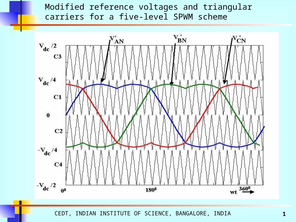
CEDT, INDIAN INSTITUTE OF SCIENCE, BANGALORE, INDIA 1
Modified reference voltages and triangular carriers for a five-level SPWM scheme

CEDT, INDIAN INSTITUTE OF SCIENCE, BANGALORE, INDIA 2
The inverter switching vectors and their switching time durations during sampling interval TS (Reference voltages are within the inner carrier region, M <
0.433)
CEDT, INDIAN INSTITUTE OF SCIENCE, BANGALORE, INDIA 3
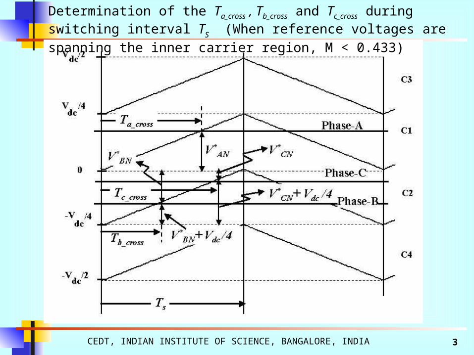
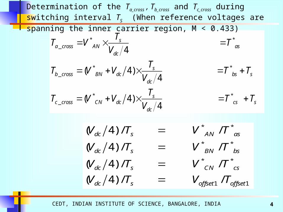
Determination of the Ta_cross , Tb_cross and Tc_cross during switching interval TS
(When reference voltages are spanning the inner carrier region, M < 0.433)
CEDT, INDIAN INSTITUTE OF SCIENCE, BANGALORE, INDIA 4
* *_
* *_
* *_
4
( 4)4
( 4)4
sa cross AN as
dc
sb cross BN dc bs s
dc
sc cross CN dc cs s
dc
TT V T
V
TT V V T T
V
TT V V T T
V
* *
* *
* *
1 1
( 4) / /
( 4) / /
( 4) / /
( 4) / /
dc s AN as
dc s BN bs
dc s CN cs
dc s offset offset
V T V T
V T V T
V T V T
V T V T
Determination of the Ta_cross , Tb_cross and Tc_cross during switching interval TS
(When reference voltages are spanning the inner carrier region, M < 0.433)

CEDT, INDIAN INSTITUTE OF SCIENCE, BANGALORE, INDIA 5
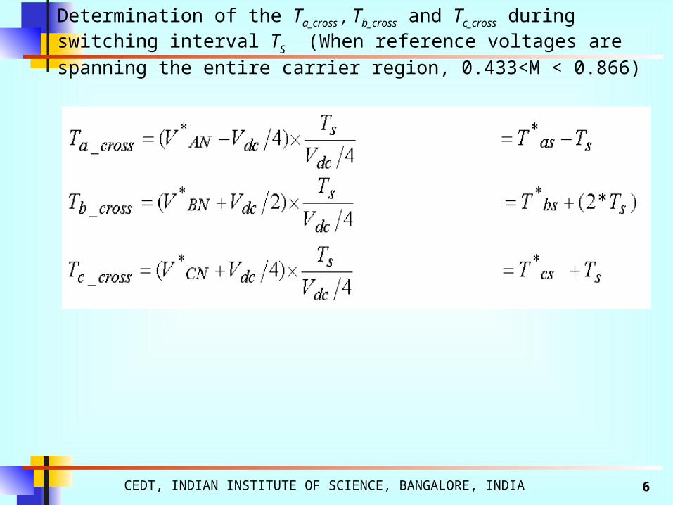
Determination of the Ta_cross , Tb_cross and Tc_cross during switching interval TS (When
reference voltages are spanning the entire carrier region, 0.433<M < 0.866)
CEDT, INDIAN INSTITUTE OF SCIENCE, BANGALORE, INDIA 6
Determination of the Ta_cross , Tb_cross and Tc_cross during switching interval TS (When
reference voltages are spanning the entire carrier region, 0.433<M < 0.866)

CEDT, INDIAN INSTITUTE OF SCIENCE, BANGALORE, INDIA 7
SUMMARY: Ta_cross , Tb_cross and Tc_cross for various carrier regions
CEDT, INDIAN INSTITUTE OF SCIENCE, BANGALORE, INDIA 8
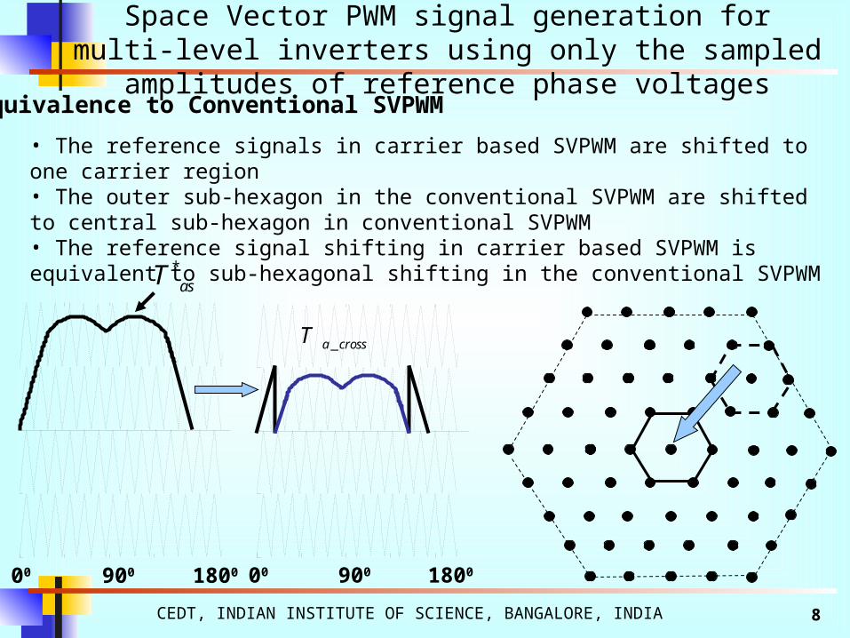
Space Vector PWM signal generation for multi-level inverters using only the sampled amplitudes of reference phase voltages
Equivalence to Conventional SVPWM
• The reference signals in carrier based SVPWM are shifted to one carrier region • The outer sub-hexagon in the conventional SVPWM are shifted to central sub-hexagon in conventional SVPWM• The reference signal shifting in carrier based SVPWM is equivalent to sub-hexagonal shifting in the conventional SVPWM
180090000
*asT
180090000
_a crossT

CEDT, INDIAN INSTITUTE OF SCIENCE, BANGALORE, INDIA 9
_ _min ( )first cross x crossT T
sec _ _( )ond cross x crossT mid T)(max __ crossxcrossthird TT , x= a, b, c
_ _middle third cross first crossT T T
0 s middleT T T
0 _ 2
2 0 _
/ 2
/ 2
first cross offset
offset first cross
T T T
T T T
_ 2
_ 2
_ 2
ga a cross offset
gb b cross offset
gc c cross offset
T T T
T T T
T T T
Algorithm for inverter leg switching time calculation

CEDT, INDIAN INSTITUTE OF SCIENCE, BANGALORE, INDIA 10
The traces of Tfirst_cross , Tsecond_cross and Tthird_cross showing non-centered time duration for middle vectors

CEDT, INDIAN INSTITUTE OF SCIENCE, BANGALORE, INDIA 11
The traces of Tg_first_cross , Tg_second_cross and Tg third_cross showing centered time duration for middle vectors

CEDT, INDIAN INSTITUTE OF SCIENCE, BANGALORE, INDIA 12
Toffset1 + Toffset2 waveforms for various modulation indices
CEDT, INDIAN INSTITUTE OF SCIENCE, BANGALORE, INDIA 13
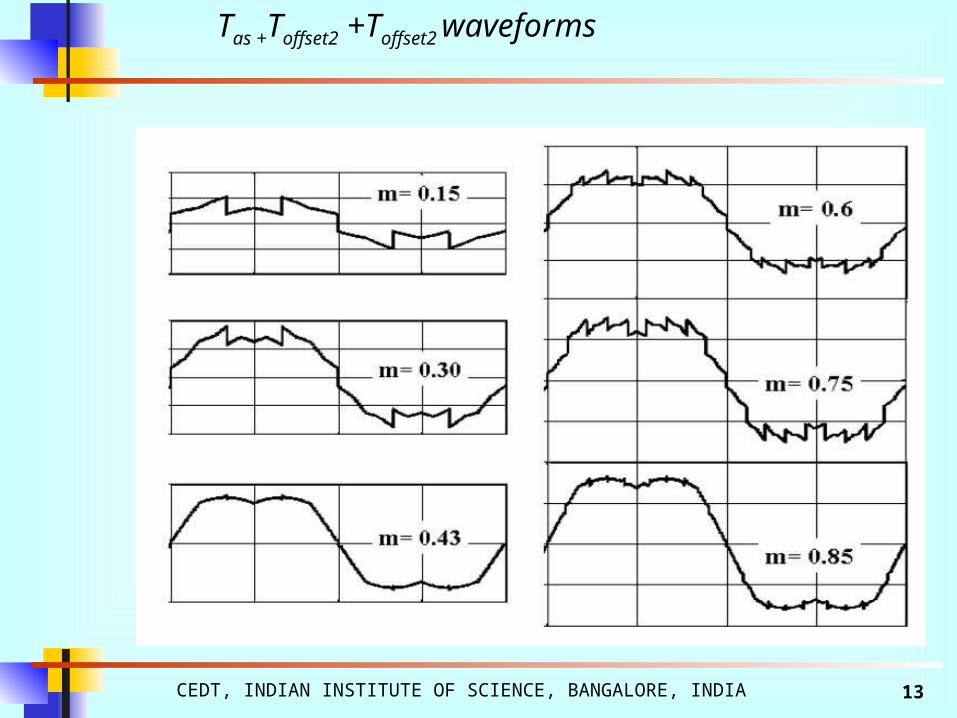
Tas +Toffset2 +Toffset2 waveforms
CEDT, INDIAN INSTITUTE OF SCIENCE, BANGALORE, INDIA 14
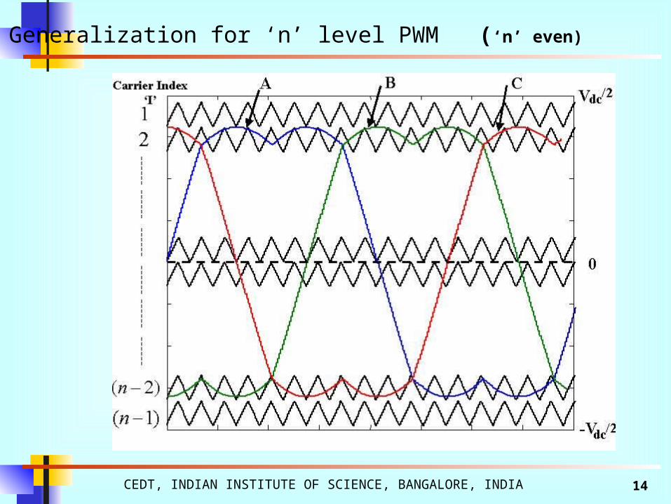
Generalization for ‘n’ level PWM (‘n’ even)
CEDT, INDIAN INSTITUTE OF SCIENCE, BANGALORE, INDIA 15
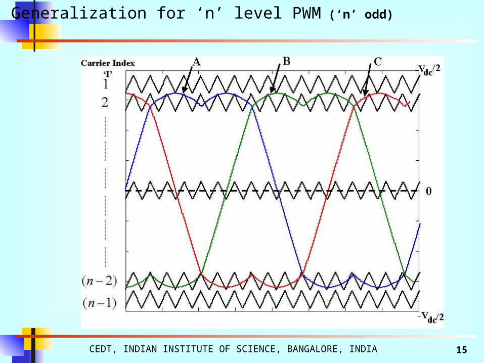
Generalization for ‘n’ level PWM (‘n’ odd)

CEDT, INDIAN INSTITUTE OF SCIENCE, BANGALORE, INDIA 16
*_
*_
*_
( / 2) (( ( / 2))* )
( / 2) (( ( / 2))* )
( / 2) (( ( / 2))* )
a cross s as a s
b cross s bs b s
c cross s cs c s
T T T I n T
T T T I n T
T T T I n T
Generalization for ‘n’ level PWM
‘n’ even
‘n’ odd
*_
*_
*_
(( ( 1) / 2)* )
(( ( 1) / 2)* )
(( ( 1) / 2)* )
a cross as a s
b cross bs b s
c cross cs c s
T T I n T
T T I n T
T T I n T

CEDT, INDIAN INSTITUTE OF SCIENCE, BANGALORE, INDIA 17
Proposed SVPWM signal generation in over-modulation
CEDT, INDIAN INSTITUTE OF SCIENCE, BANGALORE, INDIA 18
Proposed SVPWM signal generation in over-modulation
CEDT, INDIAN INSTITUTE OF SCIENCE, BANGALORE, INDIA 19
Proposed SVPWM signal generation in over-modulation

CEDT, INDIAN INSTITUTE OF SCIENCE, BANGALORE, INDIA 20
Proposed SVPWM signal generation in over-modulation
CEDT, INDIAN INSTITUTE OF SCIENCE, BANGALORE, INDIA 21
Proposed SVPWM signal generation in over-modulation
2 _offset s third crossT T T
sec _ sec _ 2g ond cross ond cross offsetT T T

CEDT, INDIAN INSTITUTE OF SCIENCE, BANGALORE, INDIA 22
Proposed SVPWM signal generation in over-modulation
2 _offset first crossT Tsec _ sec _ 2g ond cross ond cross offsetT T T
CEDT, INDIAN INSTITUTE OF SCIENCE, BANGALORE, INDIA 23
Summary: linear range of modulation

CEDT, INDIAN INSTITUTE OF SCIENCE, BANGALORE, INDIA 24
Summary: over-modulation condition
CEDT, INDIAN INSTITUTE OF SCIENCE, BANGALORE, INDIA 25
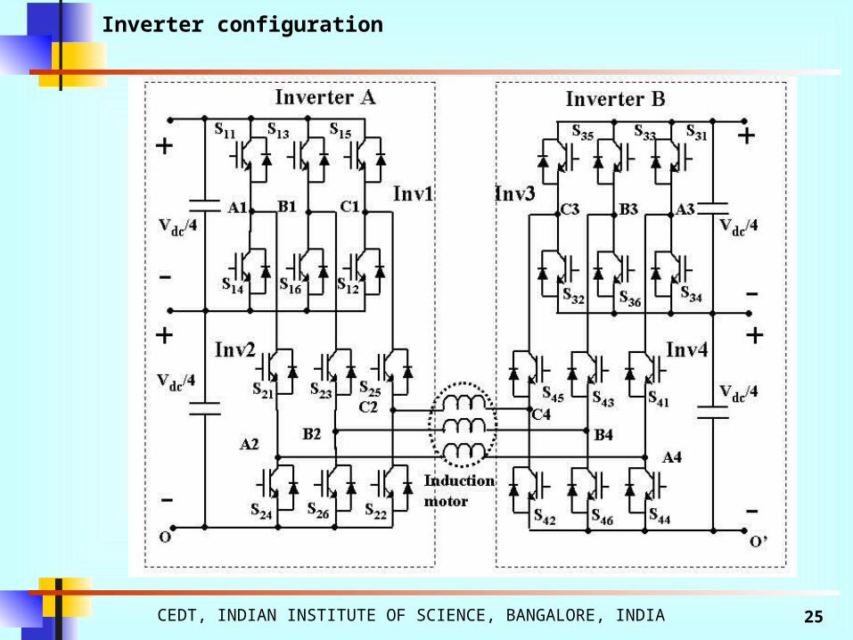
Inverter configuration

CEDT, INDIAN INSTITUTE OF SCIENCE, BANGALORE, INDIA 26
Phase-A voltage and phase-A current waveforms for modulation index 0.15 (Layer 1 operation).

CEDT, INDIAN INSTITUTE OF SCIENCE, BANGALORE, INDIA 27
Plot of Tga and offset time Toffset1 + Toffset2 for modulation index 0.15 (Layer 1 operation). [DAC output]
CEDT, INDIAN INSTITUTE OF SCIENCE, BANGALORE, INDIA 28
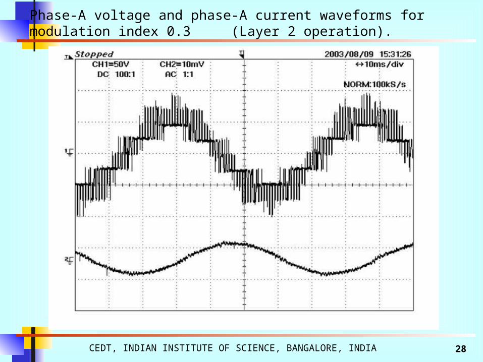
Phase-A voltage and phase-A current waveforms for modulation index 0.3 (Layer 2 operation).
CEDT, INDIAN INSTITUTE OF SCIENCE, BANGALORE, INDIA 29
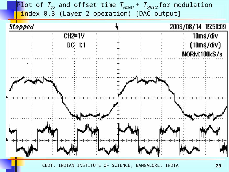
Plot of Tga and offset time Toffset1 + Toffset2 for modulation index 0.3 (Layer 2 operation) [DAC output]
CEDT, INDIAN INSTITUTE OF SCIENCE, BANGALORE, INDIA 30
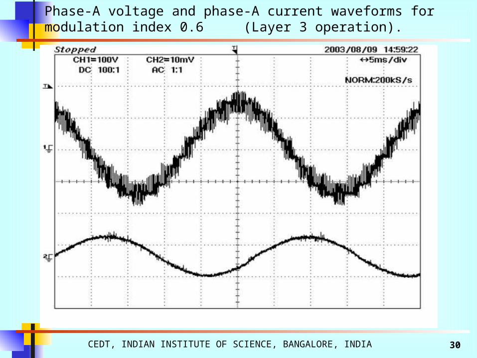
Phase-A voltage and phase-A current waveforms for modulation index 0.6 (Layer 3 operation).
CEDT, INDIAN INSTITUTE OF SCIENCE, BANGALORE, INDIA 31
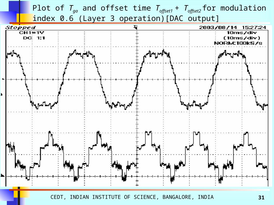
Plot of Tga and offset time Toffset1 + Toffset2 for modulation index 0.6 (Layer 3 operation)[DAC output]
CEDT, INDIAN INSTITUTE OF SCIENCE, BANGALORE, INDIA 32
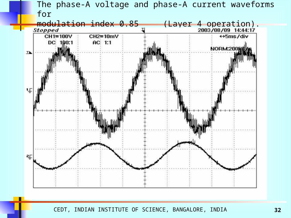
The phase-A voltage and phase-A current waveforms for modulation index 0.85 (Layer 4 operation).
CEDT, INDIAN INSTITUTE OF SCIENCE, BANGALORE, INDIA 33
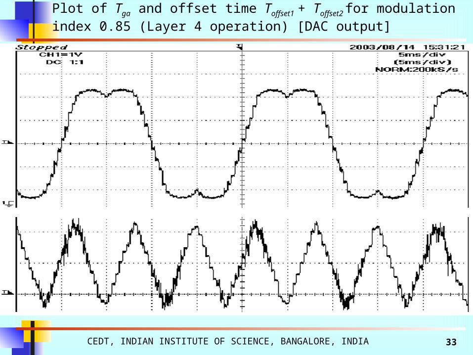
Plot of Tga and offset time Toffset1 + Toffset2 for modulation index 0.85 (Layer 4 operation) [DAC output]
CEDT, INDIAN INSTITUTE OF SCIENCE, BANGALORE, INDIA 34
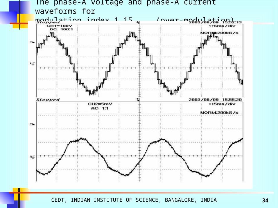
The phase-A voltage and phase-A current waveforms for modulation index 1.15 (over-modulation).

CEDT, INDIAN INSTITUTE OF SCIENCE, BANGALORE, INDIA 35
Phase-A current waveform for speed reversal from 40Hz to -40 Hz [modulation index 0.70]

CEDT, INDIAN INSTITUTE OF SCIENCE, BANGALORE, INDIA 36
Space Phasor Based Self Adaptive Current Hysteresis Controller

37
A Space Phasor Based Self Adaptive Current Hysteresis Controller Using Adjacent Inverter Voltage Vectors
with Smooth Transition to Six Step Operation for a Three Phase Voltage Source Inverter

CEDT, INDIAN INSTITUTE OF SCIENCE, BANGALORE, INDIA 38
• A self adaptive space phasor based current hysteresis controller is proposed for a voltage source inverter
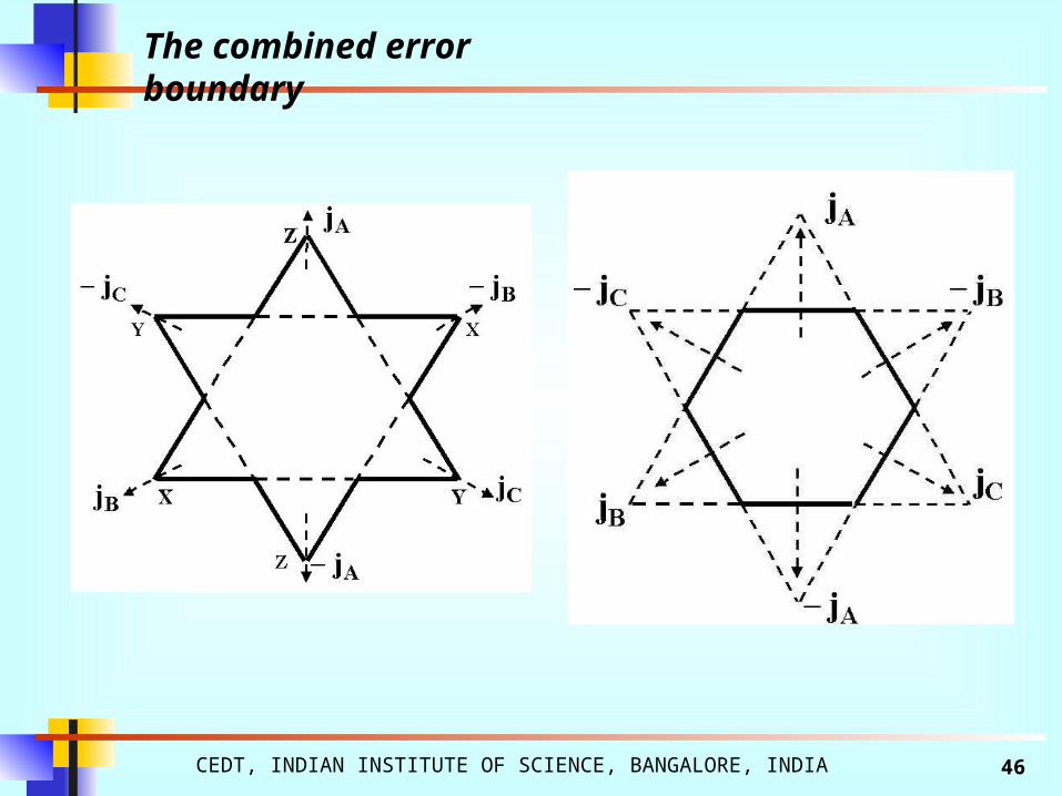
• Current error space phasor is held within a hexagonal boundary
• Current errors are monitored along jA, jB , jC axes
• Ensures optimum switching
• Does not require computations, uses simple look up table
• Uses a self adaptive sector change logic
Introduction
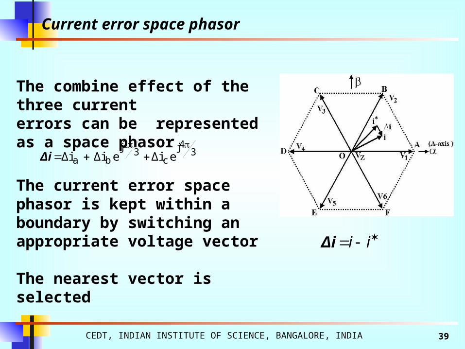
CEDT, INDIAN INSTITUTE OF SCIENCE, BANGALORE, INDIA 39
iiΔi
The combine effect of the three current errors can be represented as a space phasor
34j
c3
2jba eΔieΔi Δi
Δi
The current error space phasor is kept within a boundary by switching an appropriate voltage vector
The nearest vector is selected
Current error space phasor
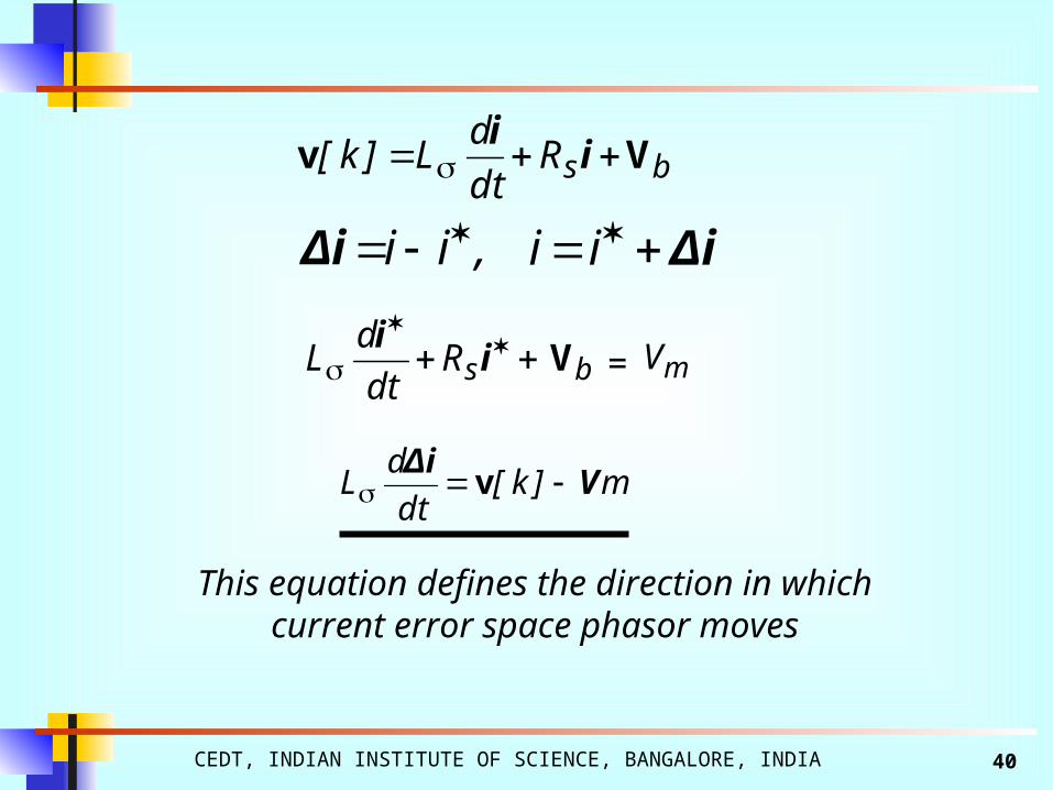
CEDT, INDIAN INSTITUTE OF SCIENCE, BANGALORE, INDIA 40
m]k[dt
dL V
Δi v
i i , Δi Δi ii
bsRdt
dL]k[ Vv i
i
bsRdt
dL V
ii
This equation defines the direction in whichcurrent error space phasor moves
= mV
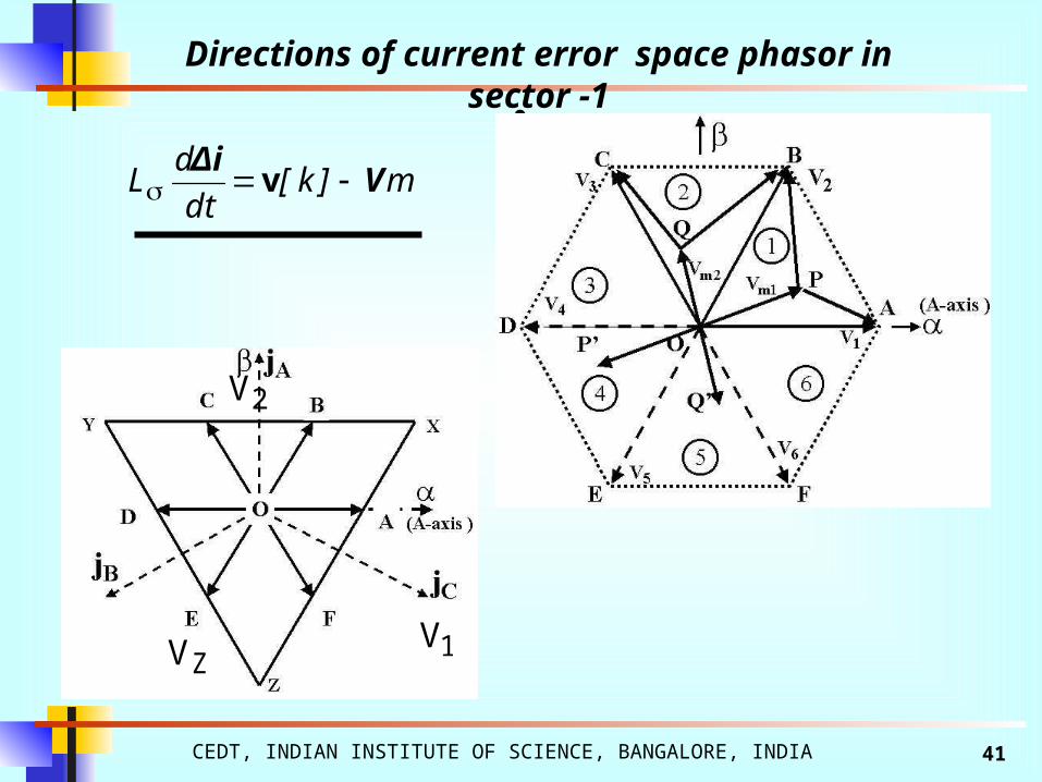
CEDT, INDIAN INSTITUTE OF SCIENCE, BANGALORE, INDIA 41
Aj
Directions of current error space phasor in sector -1
m]k[dt
dL V
Δi v
1V
2V
ZV
42
V1
V2
VZ
R1 R2
R3
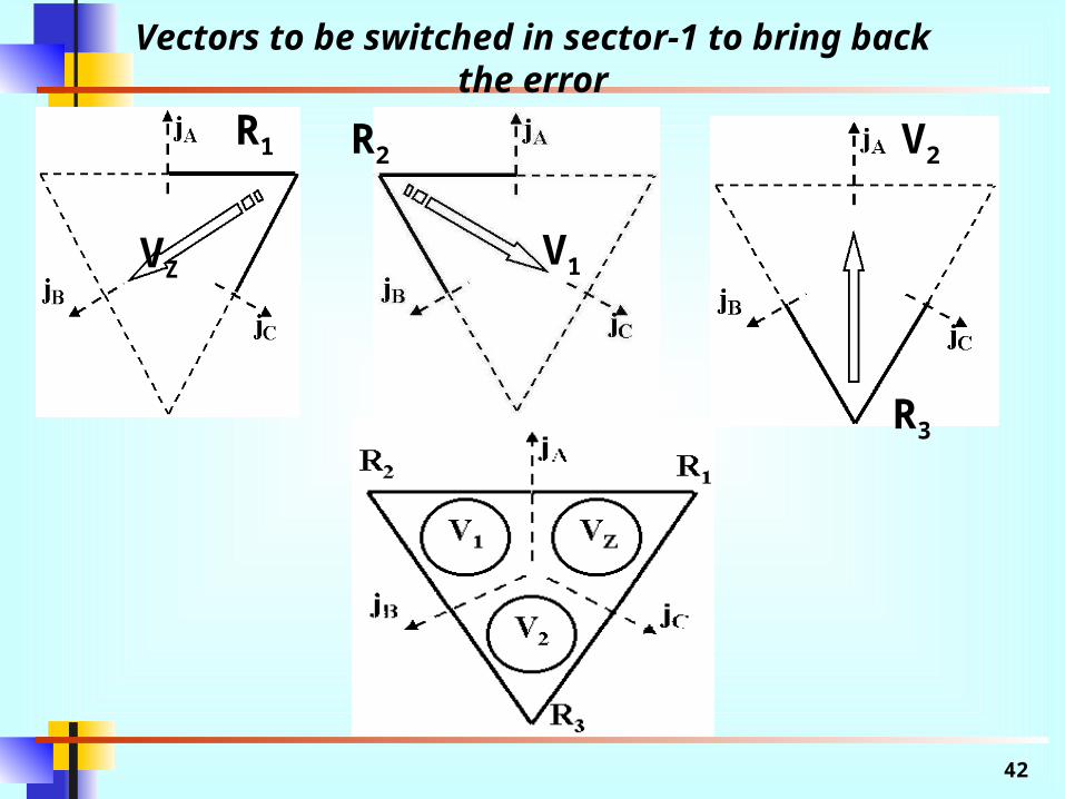
Vectors to be switched in sector-1 to bring back the error

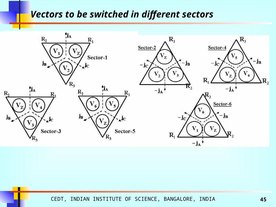
CEDT, INDIAN INSTITUTE OF SCIENCE, BANGALORE, INDIA 43
Directions of current error space phasor in sector -2
m]k[dt
dL V
Δi v
2V3V
ZV

44
V2 V3 VZ
V3
VZ
V2
1R 2R
3R
1R
3R
2R
Vectors to be switched in sector-2 to bring back the error
V3
CEDT, INDIAN INSTITUTE OF SCIENCE, BANGALORE, INDIA 45
Vectors to be switched in different sectors
CEDT, INDIAN INSTITUTE OF SCIENCE, BANGALORE, INDIA 46
The combined error boundary

47
1R
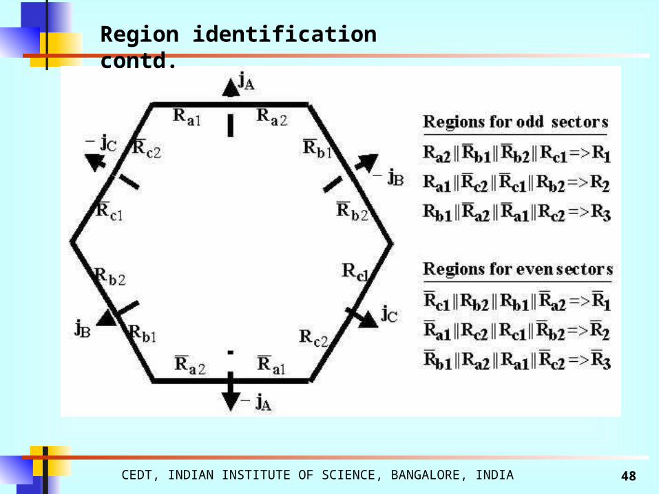
Modified regions for odd sectors
Modified regions for even sectors
Region identification
CEDT, INDIAN INSTITUTE OF SCIENCE, BANGALORE, INDIA 48
Region identification contd.
CEDT, INDIAN INSTITUTE OF SCIENCE, BANGALORE, INDIA 49
O
mVP
Q
1
2
3
4
5
6
P’1V
2V3V
4V
5V6VF
A
BC
D
ECj
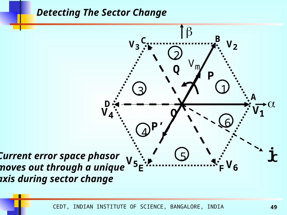
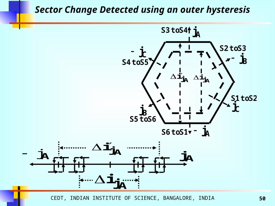
Detecting The Sector Change
Current error space phasor moves out through a uniqueaxis during sector change
CEDT, INDIAN INSTITUTE OF SCIENCE, BANGALORE, INDIA 50
Aj
Bj Cj
Aj
BjCj
AjiAji
S3toS2
S4toS3
S5toS4
S6toS5
S1toS6
S2toS1
Sector Change Detected using an outer hysteresis
Aji
AjAj Aji

CEDT, INDIAN INSTITUTE OF SCIENCE, BANGALORE, INDIA 51
AjOver modulation
Switching between the active vectors , V1 and V2
Sector 1

CEDT, INDIAN INSTITUTE OF SCIENCE, BANGALORE, INDIA 52
Over modulation
Sector change logic for over modulation region

CEDT, INDIAN INSTITUTE OF SCIENCE, BANGALORE, INDIA 53
Simulation Results
The error boundary
Sectors & Vectors
Nearest vectors are selected in every
sector
54
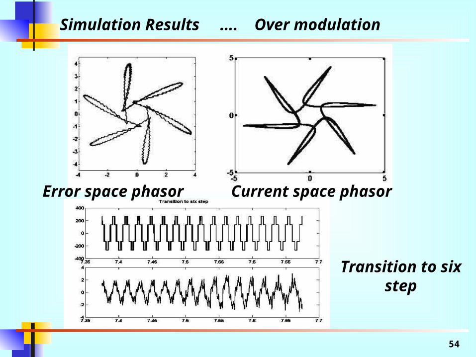
Simulation Results …. Over modulation
Transition to six step
Error space phasor Current space phasor
CEDT, INDIAN INSTITUTE OF SCIENCE, BANGALORE, INDIA 55
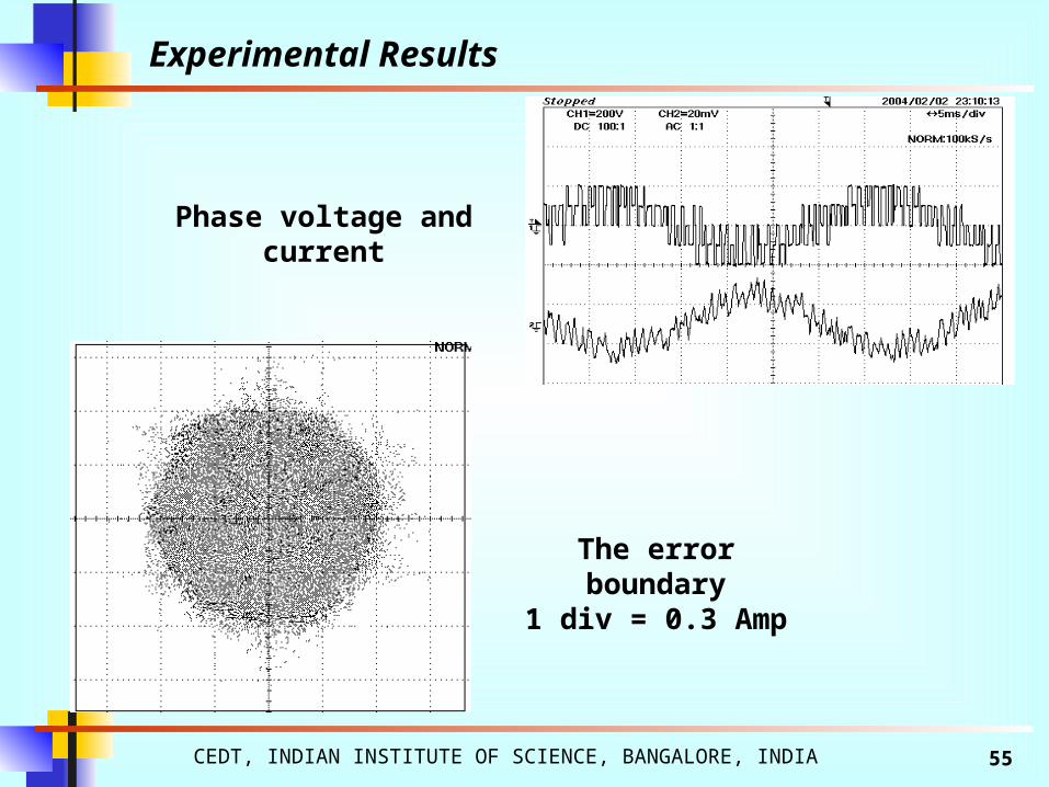
The error boundary1 div = 0.3 Amp
Phase voltage and current
Experimental Results

CEDT, INDIAN INSTITUTE OF SCIENCE, BANGALORE, INDIA 56
The machine current space phasor( no load ) 1 div = 1 amp
The machine current space phasor when loaded ( 1 div = 2 A mp )
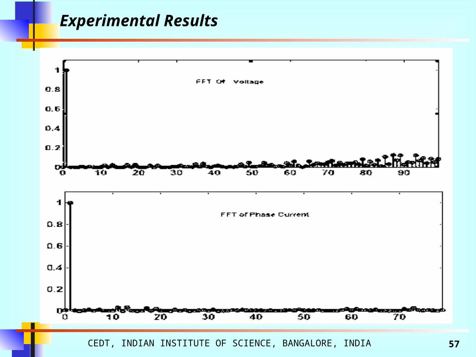
Experimental Results
CEDT, INDIAN INSTITUTE OF SCIENCE, BANGALORE, INDIA 57
Experimental Results

CEDT, INDIAN INSTITUTE OF SCIENCE, BANGALORE, INDIA 58
Experimental Results
Over modulation Six step operation
Transition to six step mode

CEDT, INDIAN INSTITUTE OF SCIENCE, BANGALORE, INDIA 59
The error boundary1 div = 1 amp
The machine current space phasor ( 1 div = 3 A mp )
Experimental Results : Over modulation

CEDT, INDIAN INSTITUTE OF SCIENCE, BANGALORE, INDIA 60
Salient Features
Space phasor based hysteresis controller with optimum switching is proposed
Self adaptive sector change logic
Smooth transition to over modulation and to six step mode
No computation of machine back emf is required
Uses simple look up tables
Ensures that only one inverter leg is switched during transition of inverter state

CEDT, INDIAN INSTITUTE OF SCIENCE, BANGALORE, INDIA 61
Current Error Space Phasor Based Hysteresis PWM Controller with Self Adaptive Logic and Adjacent Voltage Vector Selection
for The Entire Modulation Range for Three-level Voltage Source Inverter Fed Drive
CEDT, INDIAN INSTITUTE OF SCIENCE, BANGALORE, INDIA 62
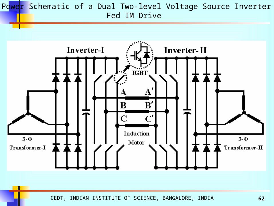
Power Schematic of a Dual Two-level Voltage Source InverterFed IM Drive

CEDT, INDIAN INSTITUTE OF SCIENCE, BANGALORE, INDIA 63
Combined Voltage Space Phasor Locations and Inverter SwitchingVector Combinations for Three-level Inverter
j 2 3 j 4 3AA BB CCv v e v e
sV
24 Sectors19 Vectors64 Switching States

CEDT, INDIAN INSTITUTE OF SCIENCE, BANGALORE, INDIA 64
Directions of Current Error Space Phasor for Tip of Vm in Sector -7
d
dt L
k mΔi V V
CEDT, INDIAN INSTITUTE OF SCIENCE, BANGALORE, INDIA 65
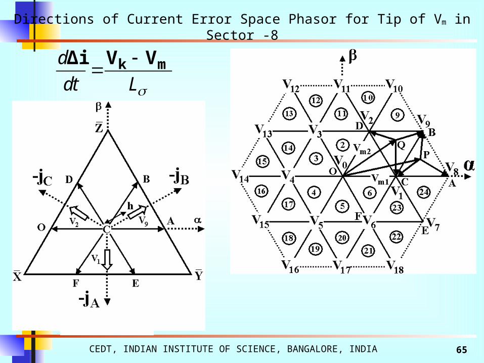
Directions of Current Error Space Phasor for Tip of Vm in Sector -8
d
dt L
k mΔi V V

CEDT, INDIAN INSTITUTE OF SCIENCE, BANGALORE, INDIA 66
Directions of Current Error Space Phasor for Tip of Vm in Sector –1 and Sector-2
d
dt L
k mΔi V V
CEDT, INDIAN INSTITUTE OF SCIENCE, BANGALORE, INDIA 67
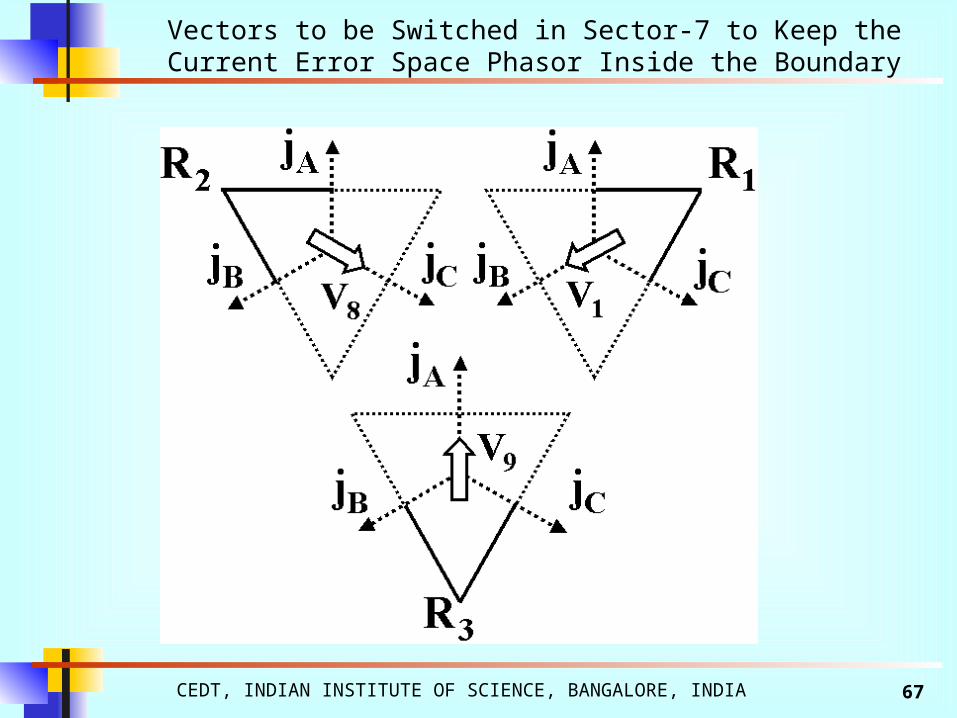
Vectors to be Switched in Sector-7 to Keep the Current Error Space Phasor Inside the Boundary
CEDT, INDIAN INSTITUTE OF SCIENCE, BANGALORE, INDIA 68
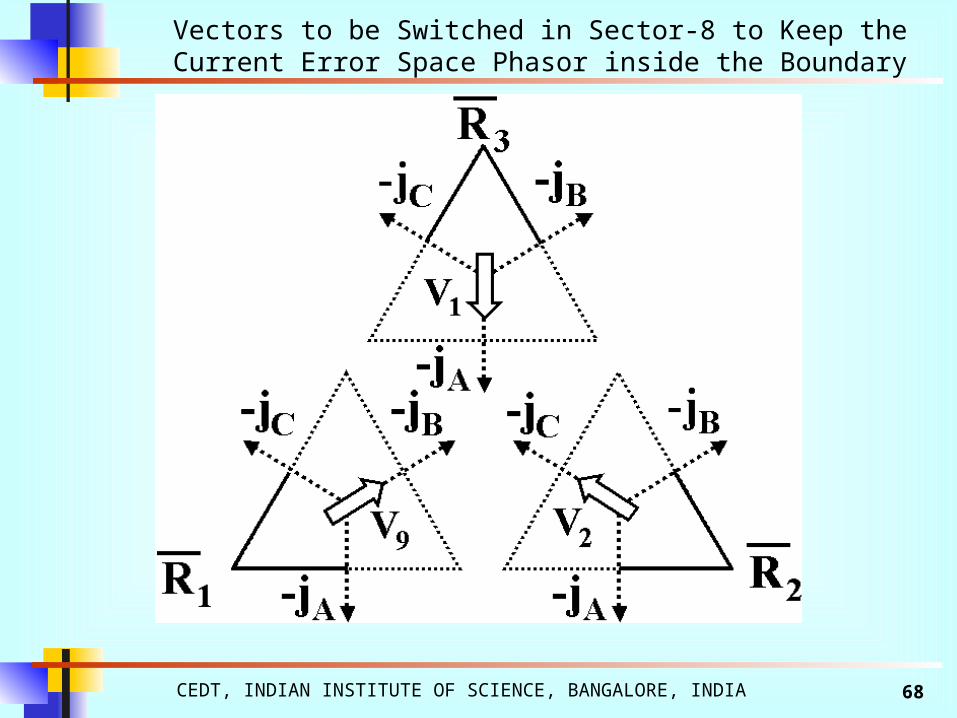
Vectors to be Switched in Sector-8 to Keep the Current Error Space Phasor inside the Boundary
CEDT, INDIAN INSTITUTE OF SCIENCE, BANGALORE, INDIA 69
Vectors to be Switched in Different Sectors for Different Regions
CEDT, INDIAN INSTITUTE OF SCIENCE, BANGALORE, INDIA 70
Vectors to be Selected in Different Sectors for Different Regions
Sector Region
R1 R2 R3 R1 R2 R3
1 V0 V1 V2 - - -
2 - - - V2 V3 V0
3 V4 V0 V3 - - -
4 - - - V0 V4 V5
5 V5 V6 V0 - - -
6 - - - V1 V0 V6
7 V1 V8 V9 - - -
: : : : : : :
24 - - - V8 V1 V7

CEDT, INDIAN INSTITUTE OF SCIENCE, BANGALORE, INDIA 71
Clamping of Inverters for Adjacent Sectors
Sector Region
R1 R2 R3 R1 R2 R3
1 87’ 17’ 27’ - - -
2 - - - 85’ 86’ 88’
3 48’ 88’ 38’ - - -
4 - - - 88’ 81’ 82’
5 57’ 67’ 77’ - - -
6 - - - 74’ 77’ 73’
7 84’ 14’ 24’ - - -
: : : : : : :
24 - - - 14’ 17’ 13’
CEDT, INDIAN INSTITUTE OF SCIENCE, BANGALORE, INDIA 72
Comparators Used for Region Detection
Aj B C
3i i i
2
A A Aj j ji i i
CEDT, INDIAN INSTITUTE OF SCIENCE, BANGALORE, INDIA 73
Region Formation from the Segments of the Hexagonal Boundary
When comparator along jA is ON and
else
B Cj jΔi Δ i [ a1R
a2R[
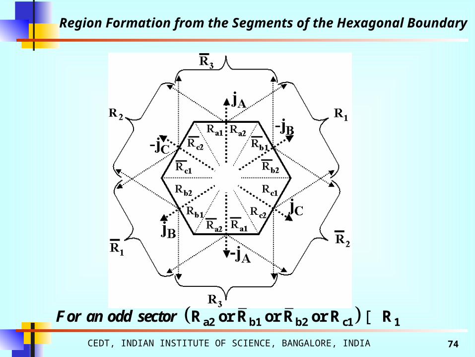
CEDT, INDIAN INSTITUTE OF SCIENCE, BANGALORE, INDIA 74
Region Formation from the Segments of the Hexagonal Boundary
a2 b1 b2 c1 1R or R or R or R RFor an odd sector [
CEDT, INDIAN INSTITUTE OF SCIENCE, BANGALORE, INDIA 75
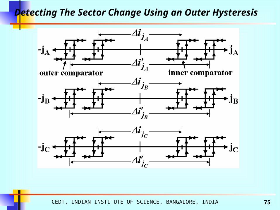
Detecting The Sector Change Using an Outer Hysteresis

CEDT, INDIAN INSTITUTE OF SCIENCE, BANGALORE, INDIA 76
Sector Change Detection for Two-level Operation (Trajectory ‘a’)
Current error space phasor moves out through a uniqueaxis during a sector change
CEDT, INDIAN INSTITUTE OF SCIENCE, BANGALORE, INDIA 77
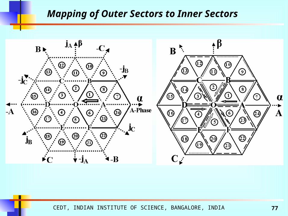
Mapping of Outer Sectors to Inner Sectors
CEDT, INDIAN INSTITUTE OF SCIENCE, BANGALORE, INDIA 78
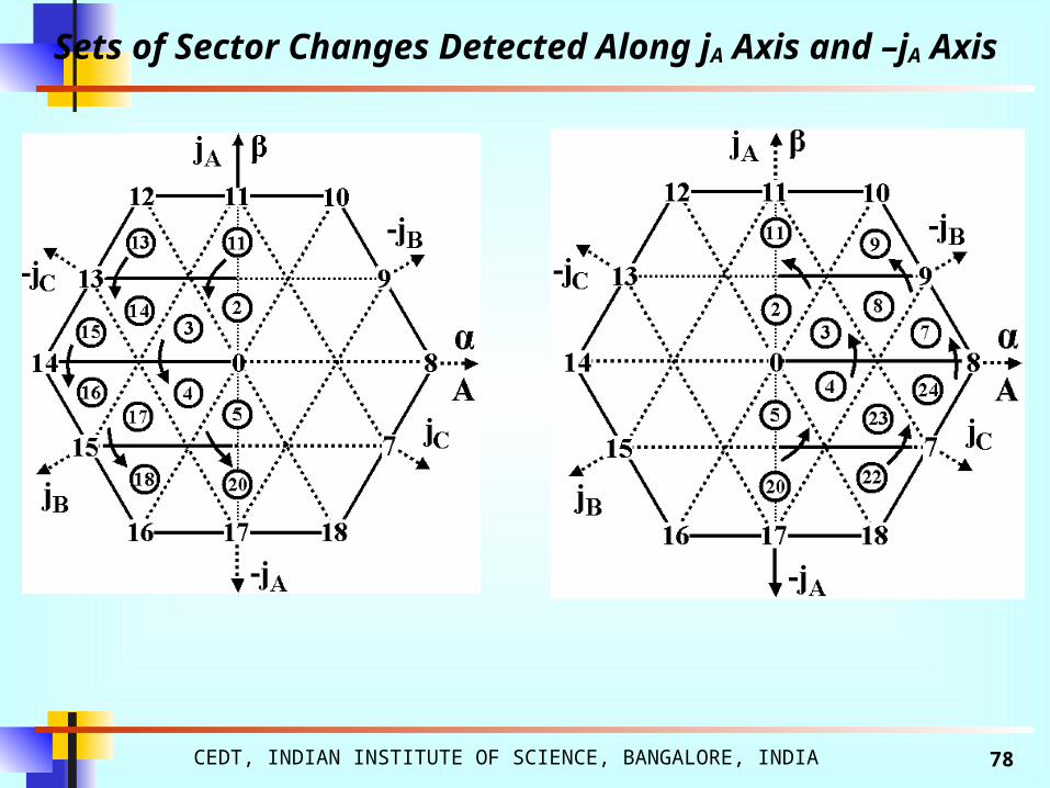
Sets of Sector Changes Detected Along jA Axis and –jA Axis
CEDT, INDIAN INSTITUTE OF SCIENCE, BANGALORE, INDIA 79
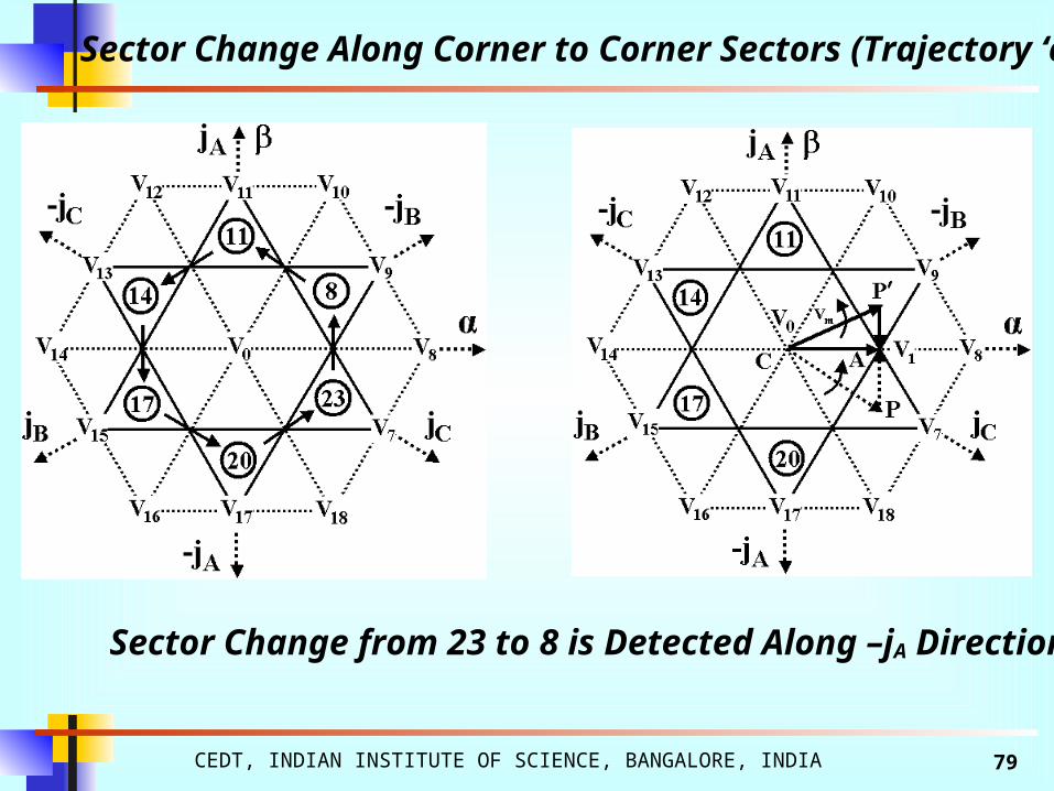
Sector Change Along Corner to Corner Sectors (Trajectory ‘c’)
Sector Change from 23 to 8 is Detected Along –jA Direction

CEDT, INDIAN INSTITUTE OF SCIENCE, BANGALORE, INDIA 80
Prevention of Jitter Prevention of False Sector Change

CEDT, INDIAN INSTITUTE OF SCIENCE, BANGALORE, INDIA 81
Sector Change During Over Modulation (Trajectory ‘f’)

CEDT, INDIAN INSTITUTE OF SCIENCE, BANGALORE, INDIA 82
Sector Change During Over Modulation (Sector-7 to Sector-9)
Trajectory of Current Error Space Phasor

CEDT, INDIAN INSTITUTE OF SCIENCE, BANGALORE, INDIA 83
Sector Change During Over Modulation (Sector-9 to Sector-10)
Trajectory of Current Error Space Phasor
CEDT, INDIAN INSTITUTE OF SCIENCE, BANGALORE, INDIA 84
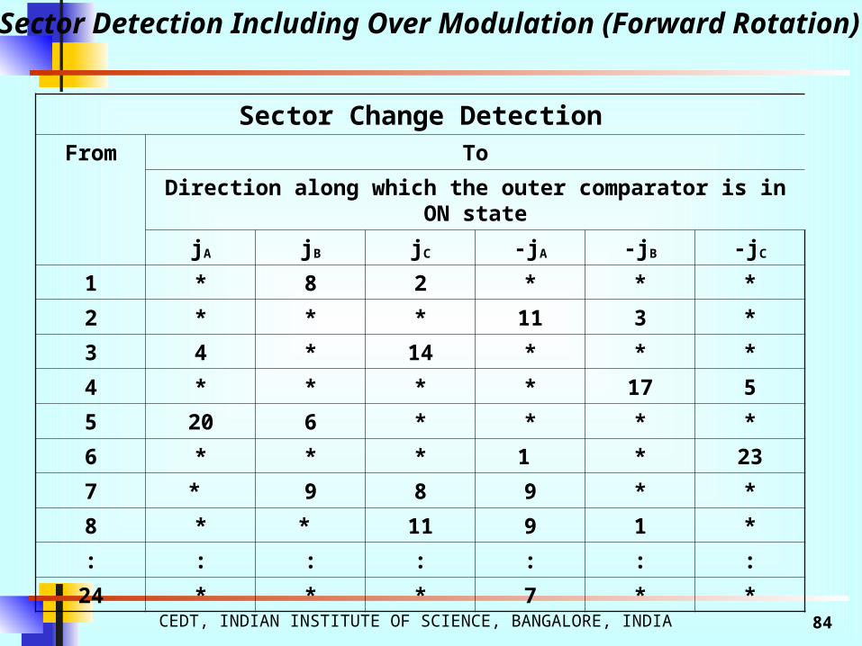
Sector Detection Including Over Modulation (Forward Rotation)
Sector Change DetectionFrom To
Direction along which the outer comparator is in ON state
jA jB jC -jA -jB -jC
1 * 8 2 * * *
2 * * * 11 3 *
3 4 * 14 * * *
4 * * * * 17 5
5 20 6 * * * *
6 * * * 1 * 23
7 * 9 8 9 * *
8 * * 11 9 1 *
: : : : : : :
24 * * * 7 * *
CEDT, INDIAN INSTITUTE OF SCIENCE, BANGALORE, INDIA 85
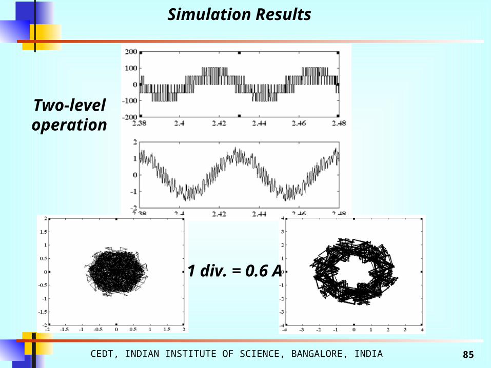
Simulation Results
Two-leveloperation
1 div. = 0.6 A

CEDT, INDIAN INSTITUTE OF SCIENCE, BANGALORE, INDIA 86
Simulation Results
Transition from two-level
to three-level
Transition from three-level
to over modulation

CEDT, INDIAN INSTITUTE OF SCIENCE, BANGALORE, INDIA 87
Simulation Results
Three-leveloperation
1 div. = 0.6 A
CEDT, INDIAN INSTITUTE OF SCIENCE, BANGALORE, INDIA 88
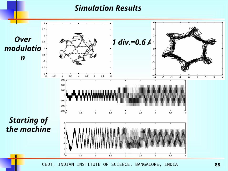
Simulation Results
Overmodulation
1 div.=0.6 A
Starting of the machine
CEDT, INDIAN INSTITUTE OF SCIENCE, BANGALORE, INDIA 89
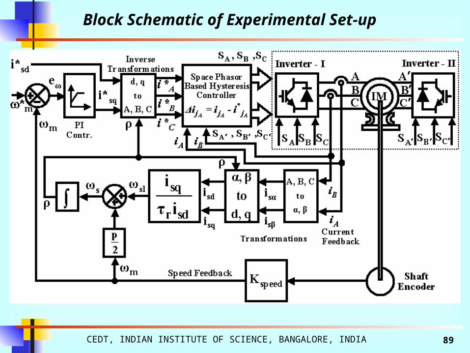
Block Schematic of Experimental Set-up

CEDT, INDIAN INSTITUTE OF SCIENCE, BANGALORE, INDIA 90
1 div = 0.3 Amp
Two-leveloperation
Experimental Results
1 div = 0.75Amp

CEDT, INDIAN INSTITUTE OF SCIENCE, BANGALORE, INDIA 91
Transition form two-level to
three-level and vice versa
Experimental Results

CEDT, INDIAN INSTITUTE OF SCIENCE, BANGALORE, INDIA 921 div = 0.3 Amp
Three-leveloperation
Experimental Results
1 div = 0.75Amp
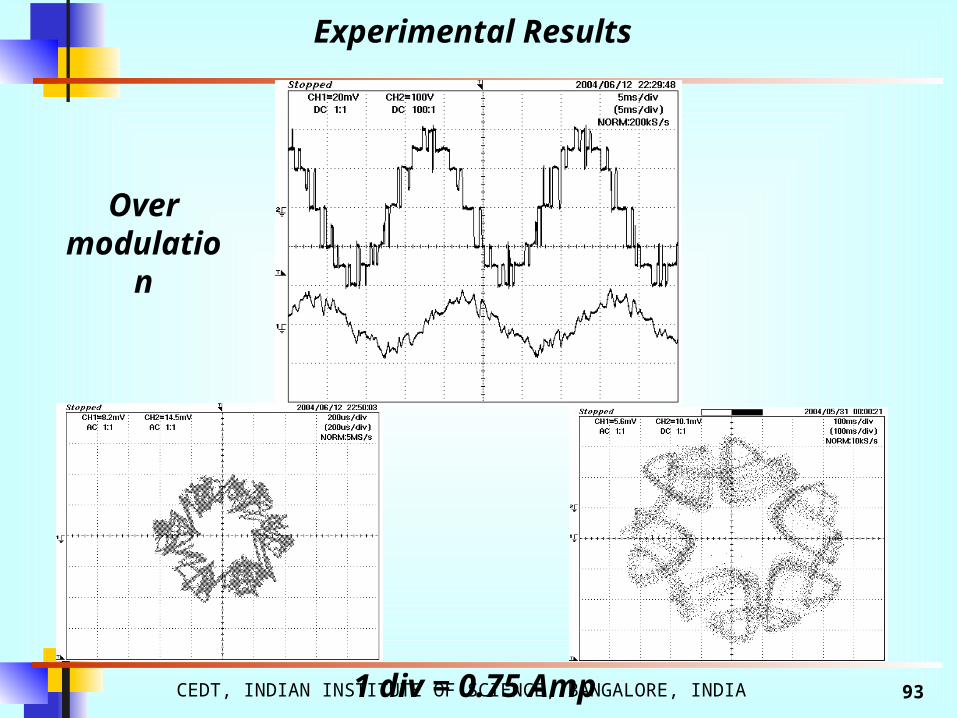
CEDT, INDIAN INSTITUTE OF SCIENCE, BANGALORE, INDIA 931 div = 0.75 Amp
Overmodulation
Experimental Results
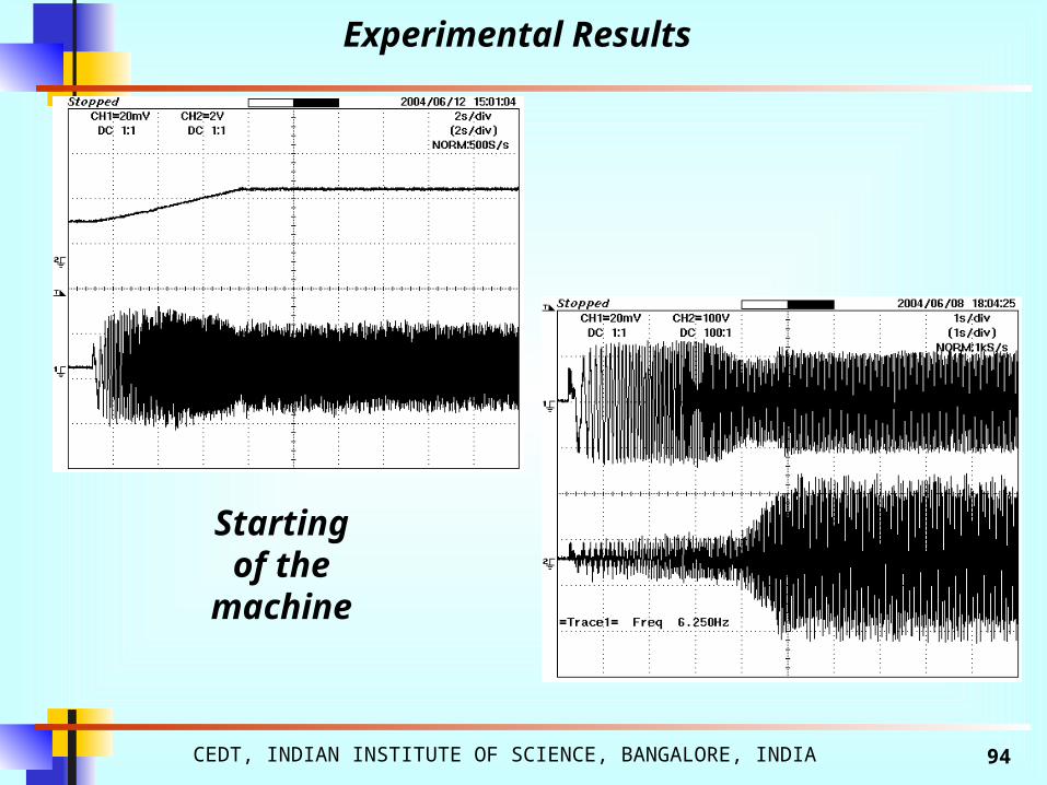
CEDT, INDIAN INSTITUTE OF SCIENCE, BANGALORE, INDIA 94
Starting of the
machine
Experimental Results

CEDT, INDIAN INSTITUTE OF SCIENCE, BANGALORE, INDIA 95
Speed reversal of
the machine
Experimental Results
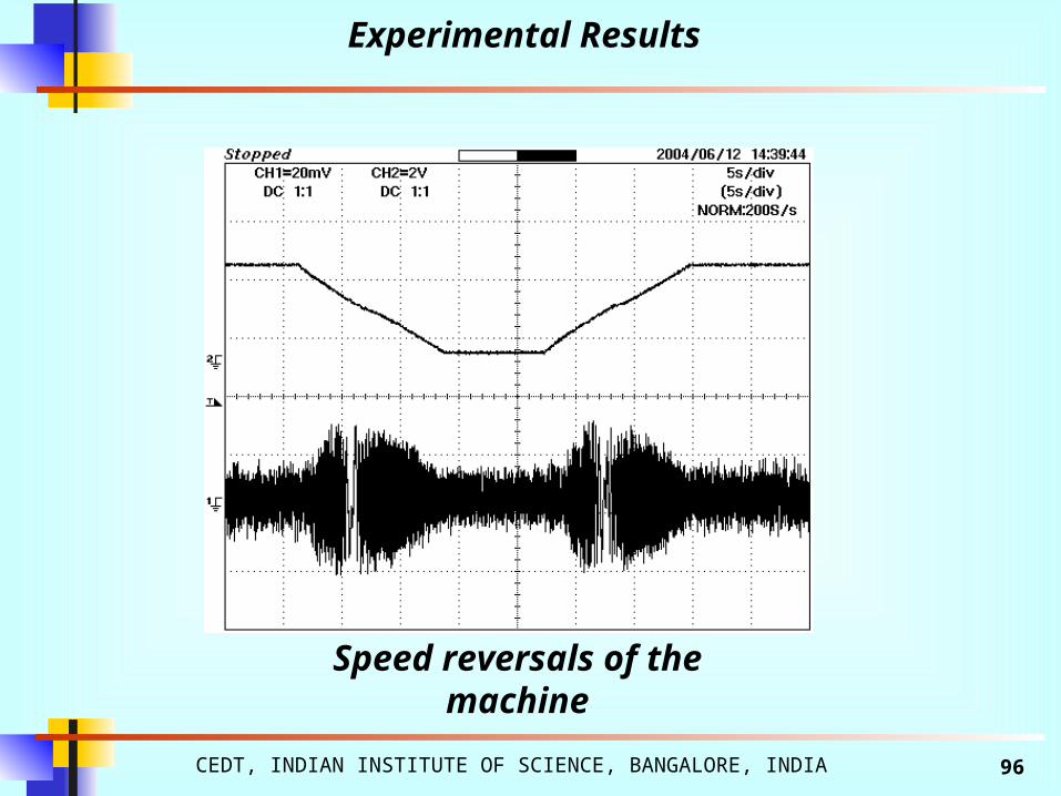
CEDT, INDIAN INSTITUTE OF SCIENCE, BANGALORE, INDIA 96
Speed reversals of the machine
Experimental Results

CEDT, INDIAN INSTITUTE OF SCIENCE, BANGALORE, INDIA 97
Normalized harmonic spectrum
of current waveforms
Two-level operation
Experimental Results
Three-level operation
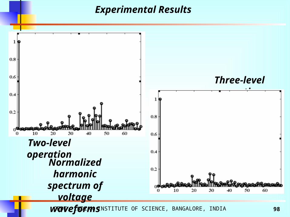
CEDT, INDIAN INSTITUTE OF SCIENCE, BANGALORE, INDIA 98
Normalized harmonic spectrum
of voltage waveforms
Two-level operation
Experimental Results
Three-level operation
A HARMONIC ELIMINATION SCHEME FOR AN OPEN – END WINDING INDUCTION MOTOR DRIVE FED FROM
TWO INVERTERS WITH ASYMMETRICAL DC LINK VOLTAGES
CEDT, INDIAN INSTITUTE OF SCIENCE, BANGALORE, INDIA 100
A low order harmonic elimination technique for an open–end winding induction motor drive is proposed.
For the present open–end winding drive, the induction motor is fed from two 2-level inverters with different isolated DC-link voltages of ratio equal to 1:0.366.
With such a scheme it is found that all the 5th and 7th order (6n 1, where n = 1,3,5,7 etc.) harmonics are absent in the motor phase voltage.
The third harmonic order currents are eliminated from the motor by using isolated DC-link supply for the two inverters.
A smooth transition to the over-modulation region is also achievable from the present open– end winding IM drive.
Salient features
CEDT, INDIAN INSTITUTE OF SCIENCE, BANGALORE, INDIA 101
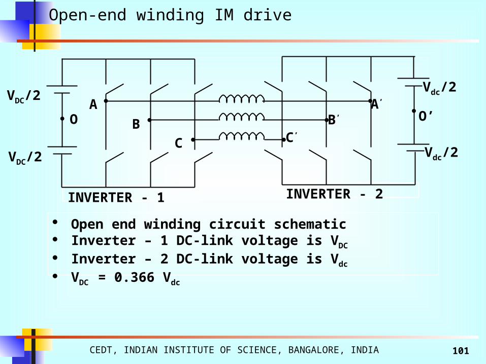
Open end winding circuit schematic Inverter – 1 DC-link voltage is VDC
Inverter – 2 DC-link voltage is Vdc
VDC = 0.366 Vdc
INVERTER - 2
O
INVERTER - 1
A
B
C C’
B’
A’
O’
Vdc/2
Vdc/2
VDC/2
VDC/2
Open-end winding IM drive

CEDT, INDIAN INSTITUTE OF SCIENCE, BANGALORE, INDIA 102
Vector diagram inverter – 1Vector magnitude = VDC
VDC4 (-++)
4’(-++)
1’(+--)
6’(+-+)5’(--+)
2’(++-)3’(-+-)
5 (--+) 6 (+-+)
1 (+--)
2 (++-)3 (-+-)
Vector diagram inverter – 2Vector magnitude = Vdc
Voltage space phasor diagrams of individual inverters
0.366 VDC

CEDT, INDIAN INSTITUTE OF SCIENCE, BANGALORE, INDIA 103
30
30
6’ 1,1’ (+--) 2,2’ (++-) 3,3’ (-+-) 4,4’ (-++) 5,5’ (--+) 6,6’ (+-+) 7,7’ (+++) 8,8’ (---)
1
23
4
5`
6
3’5’
4’1’
6’
2’
1’ 3’ 2’ 4’
5’
450
1.223 VDC
VDC
VDC sin150 = k VDC sin450 So k = sin150 / sin450 = 0.366
150
1200 k VDC
Selected combinations of the vector positions from inverter – 1 and inverter – 2 and calculation of DC – link voltage ratio (k) for both the inverters.
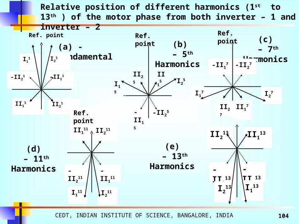
CEDT, INDIAN INSTITUTE OF SCIENCE, BANGALORE, INDIA 104
(a) - Fundamental
II21II1
1
-II21 -II1
1
I11 I2
1
Ref. point
(b) – 5th Harmonics
-II15 -II2
5
II15II2
5
I15 I2
5
Ref. point (c) – 7th Harmonics
-II17 -II2
7
I27I1
7
II17II2
7
Ref. point
(d) – 11th Harmonics
-II211 -II1
11
I111 I2
11
II211II1
11
Ref. point
(e) – 13th Harmonics
-II113 -II2
13
I113I2
13
II213 II1
13
Relative position of different harmonics (1st to 13th ) of the motor phase from both inverter – 1 and inverter – 2
CEDT, INDIAN INSTITUTE OF SCIENCE, BANGALORE, INDIA 105
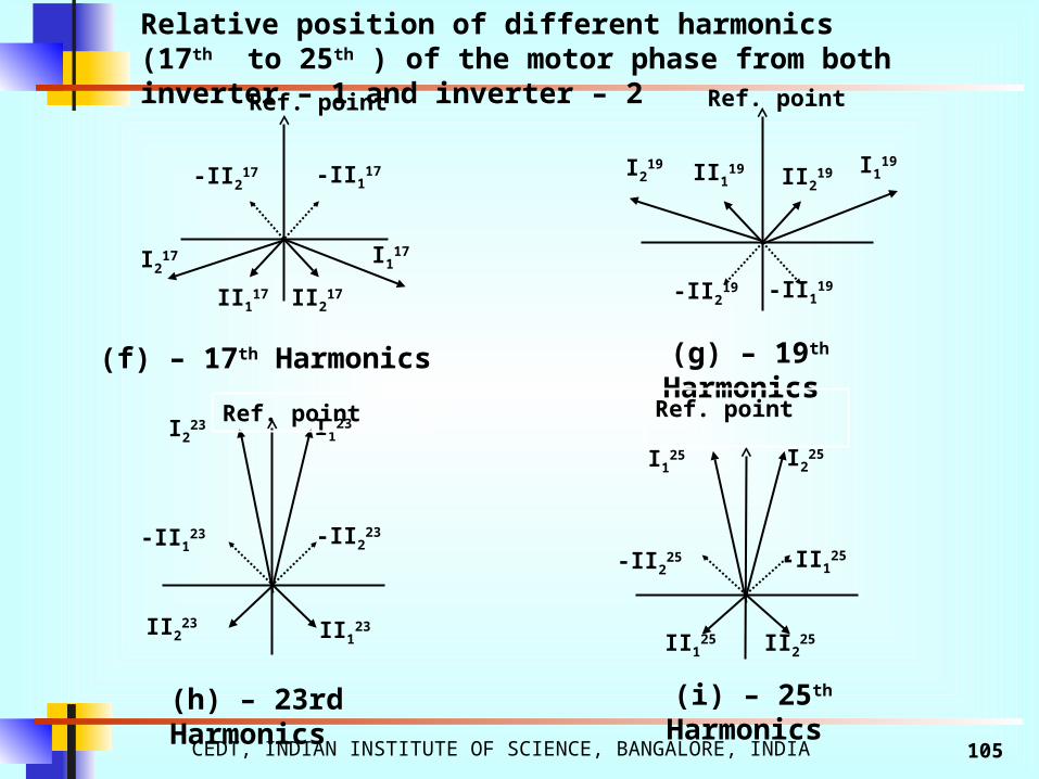
Relative position of different harmonics (17th to 25th ) of the motor phase from both inverter – 1 and inverter – 2
(f) – 17th Harmonics (g) – 19th Harmonics
II223 II1
23
-II123
I223 I1
23
-II223
(h) – 23rd Harmonics (i) – 25th Harmonics
II117 II2
17
I217 I1
17
-II217 -II1
17
Ref. point
-II219 -II1
19
II219II1
19 I119I2
19
Ref. point
Ref. point
II125 II2
25
-II125-II2
25
I125 I2
25
Ref. point

CEDT, INDIAN INSTITUTE OF SCIENCE, BANGALORE, INDIA 106
60
VCO t
VAO
VBO
Switching vectors and pole voltage (VAO , VBO , VCO ) of inverter-1
16655433221 4I 1
360300240180120600
VA’O
VB’O
VC’O t
3423153 4 6 15 6 2II
3603002401801200
Switching vectors and pole voltage (VA’O , VB’O , VC’O ) of inverter - 2

CEDT, INDIAN INSTITUTE OF SCIENCE, BANGALORE, INDIA 107
EXPERIMENTAL RESULTS
OVER MODULATION
Phase voltage
Harmonic spectrum
Phase current
Phase current and Fourier spectrum
show absence of all 6n±1 (n = 1,3,5 .. etc) harmonics
Y- axis : 75v/div
Y- axis : 1 amp/div

CEDT, INDIAN INSTITUTE OF SCIENCE, BANGALORE, INDIA 108
EXPERIMENTAL RESULTS
MODULATING WAVE,TRIANGLE CARRIER WAVE AND CORRESPONDING GATE SIGNAL
a – Modulating wave and triangle carrier wave (inverter-1). b – Inverter-1 pole voltage. c – Modulating wave and triangle carrier wave (inverter-2). d – Inverter-2 pole voltage (fc = 6f)
Phase-A and A’
Phase-B and B’
Phase-C and C’
a
b
c
d
a
b
c
d
a
b
c
d
CEDT, INDIAN INSTITUTE OF SCIENCE, BANGALORE, INDIA 109
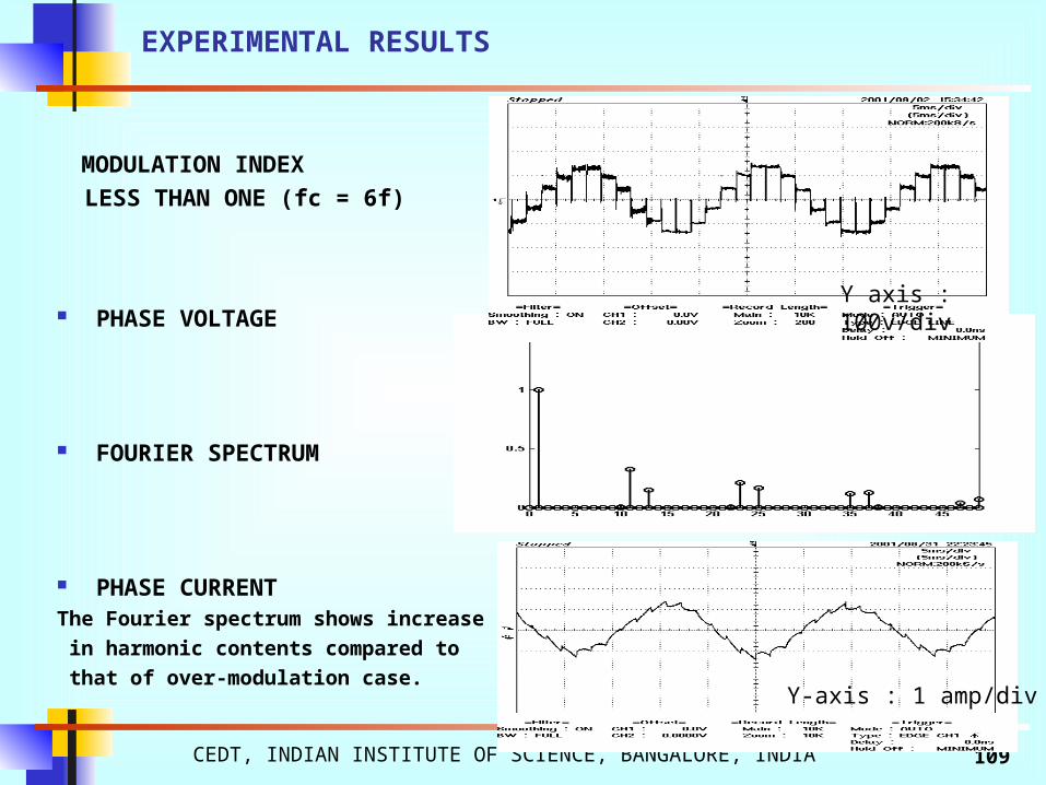
EXPERIMENTAL RESULTS
MODULATION INDEX LESS THAN ONE (fc = 6f)
PHASE VOLTAGE
FOURIER SPECTRUM
PHASE CURRENTThe Fourier spectrum shows increase in harmonic contents compared to that of over-modulation case.
Y axis : 100v/div
Y-axis : 1 amp/div
CEDT, INDIAN INSTITUTE OF SCIENCE, BANGALORE, INDIA 110
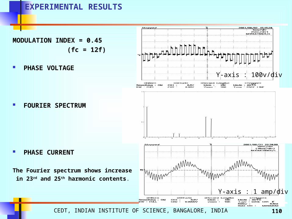
EXPERIMENTAL RESULTS
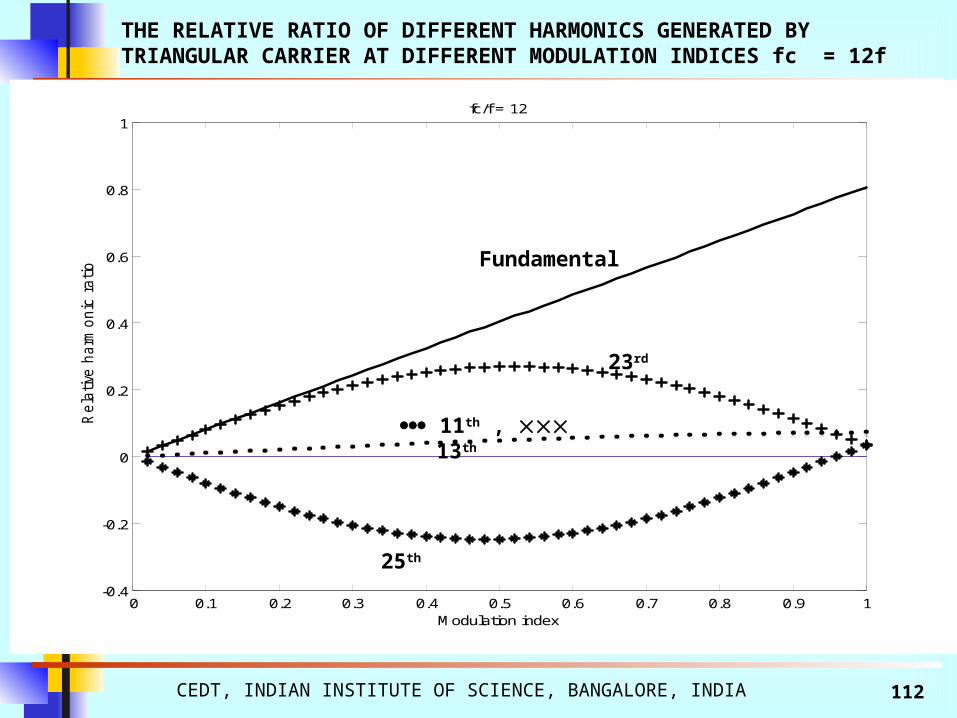
MODULATION INDEX = 0.45 (fc = 12f)
PHASE VOLTAGE
FOURIER SPECTRUM
PHASE CURRENT
The Fourier spectrum shows increase in 23rd and 25th harmonic contents.
0 5 10 15 20 25 30 35 40 450
0.5
1
1.5
Y-axis : 100v/div
Y-axis : 1 amp/div
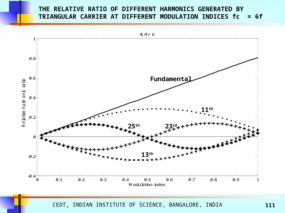
CEDT, INDIAN INSTITUTE OF SCIENCE, BANGALORE, INDIA 111
0 0.1 0.2 0.3 0.4 0.5 0.6 0.7 0.8 0.9 1-0.4
-0.2
0
0.2
0.4
0.6
0.8
1fc/f = 6
Modulation index
Rela
tive
harm
onic
ratio Fundamental
11th
25th 23rd
13th
THE RELATIVE RATIO OF DIFFERENT HARMONICS GENERATED BY TRIANGULAR CARRIER AT DIFFERENT MODULATION INDICES fc = 6f
CEDT, INDIAN INSTITUTE OF SCIENCE, BANGALORE, INDIA 112
THE RELATIVE RATIO OF DIFFERENT HARMONICS GENERATED BY TRIANGULAR CARRIER AT DIFFERENT MODULATION INDICES fc = 12f
0 0.1 0.2 0.3 0.4 0.5 0.6 0.7 0.8 0.9 1-0.4
-0.2
0
0.2
0.4
0.6
0.8
1fc/f = 12
Modulation index
Rela
tive
harm
onic
ratio Fundamental
23rd
11th , 13th
25th
CEDT, INDIAN INSTITUTE OF SCIENCE, BANGALORE, INDIA 113
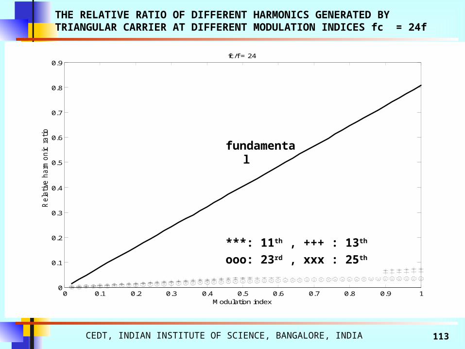
THE RELATIVE RATIO OF DIFFERENT HARMONICS GENERATED BY TRIANGULAR CARRIER AT DIFFERENT MODULATION INDICES fc = 24f
0 0.1 0.2 0.3 0.4 0.5 0.6 0.7 0.8 0.9 10
0.1
0.2
0.3
0.4
0.5
0.6
0.7
0.8
0.9fc/f = 24
Modulation index
Rela
tive
harm
onic
ratio
fundamental
***: 11th , +++ : 13th
ooo: 23rd , xxx : 25th
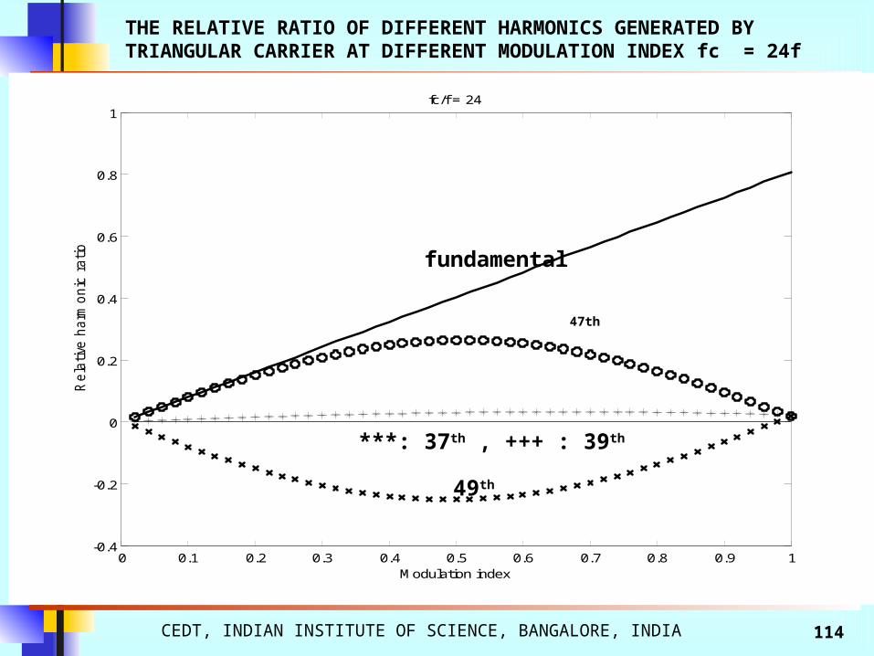
CEDT, INDIAN INSTITUTE OF SCIENCE, BANGALORE, INDIA 114
THE RELATIVE RATIO OF DIFFERENT HARMONICS GENERATED BY TRIANGULAR CARRIER AT DIFFERENT MODULATION INDEX fc = 24f
fundamental
0 0.1 0.2 0.3 0.4 0.5 0.6 0.7 0.8 0.9 1-0.4
-0.2
0
0.2
0.4
0.6
0.8
1fc/f = 24
Modulation index
Rela
tive
harm
onic
ratio
fundamental
47th
***: 37th , +++ : 39th
49th
CEDT, INDIAN INSTITUTE OF SCIENCE, BANGALORE, INDIA 115
All the 6n 1, n = 1, 3, 5 etc,. order harmonics are eliminated from the motor phase voltage in the entire speed range.
A linear transition to the maximum modulation is possible.
By properly choosing the frequency modulation ratio (6, 12, 24, 48) at different speed ranges, the switching frequency of both inverters can be controlled within 500hz.
In the extreme speed range the lower voltage inverter is
switched more frequently than the higher voltage inverter. The 11th and 13th order harmonic voltage amplitudes in the
motor phase voltage can be suppressed by introducing notches in the modulating wave.
The resultant fundamental is reduced to 99.57%. The resultant 11th order harmonic is reduced to 50%.
And the 13th order harmonic is reduced to 31.86%.
CONCLUSION & SALIENT FEATURES

CEDT, INDIAN INSTITUTE OF SCIENCE, BANGALORE, INDIA 116
a – Modulating wave (11th and 13th harmonics suppressed) and triangle carrier wave (inverter-1)
b – Inverter-1 pole voltage
c – Modulating wave (11th and 13th harmonics suppressed) and triangle carrier wave (inverter-2)
d – Inverter-2 pole voltage
EXPERIMENTAL RESULTS: 11th and 13th suppression
Pole voltage of inverter-2 ( Over modulation)
Pole voltage of inverter-1 ( Over modulation)
Modulating wave and triangular carrier wave (over modulation ) fc/f = 12
CEDT, INDIAN INSTITUTE OF SCIENCE, BANGALORE, INDIA 117
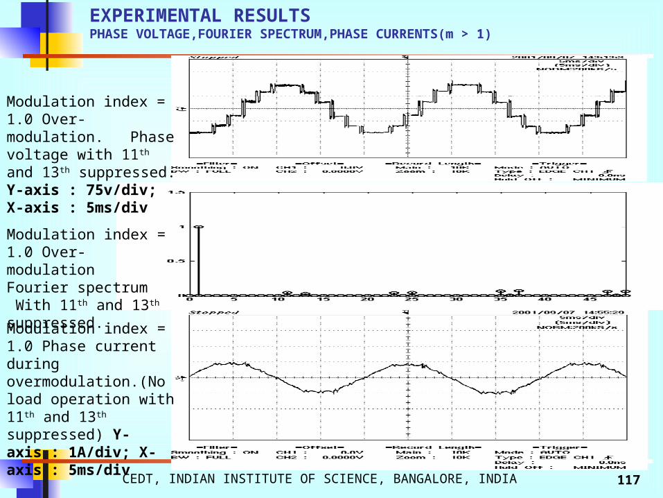
EXPERIMENTAL RESULTSPHASE VOLTAGE,FOURIER SPECTRUM,PHASE CURRENTS(m > 1)
Modulation index = 1.0 Over-modulation. Phase voltage with 11th and 13th suppressed. Y-axis : 75v/div; X-axis : 5ms/div
Modulation index = 1.0 Over-modulation Fourier spectrum With 11th and 13th suppressed.
Modulation index = 1.0 Phase current during overmodulation.(No load operation with 11th and 13th suppressed) Y-axis : 1A/div; X-axis : 5ms/div

CEDT, INDIAN INSTITUTE OF SCIENCE, BANGALORE, INDIA 118
EXPERIMENTAL RESULTSPHASE VOLTAGE,FOURIER SPECTRUM,PHASE CURRENTS(m > 0.9)
Y- axis : 1A/div
Y- axis : 75v/div
Modulation index = 0.9. Phase voltage. fc = 12f, With 11th and 13th suppressed. Y-axis : 75v/div; X-axis : 5ms/div
Modulation index = 0.9. fourier spectrum. fc = 12f.
With 11th and 13th suppressed
Modulation index = 0.9. Phase current waveform. fc = 12f ( no load operation with 11th and 13th suppressed). Y-axis : 1A/div; X-axis : 5ms/div

CEDT, INDIAN INSTITUTE OF SCIENCE, BANGALORE, INDIA 119
EXPERIMENTAL RESULTSPHASE VOLTAGE,FOURIER SPECTRUM,PHASE CURRENTS(m > 0.45)
Y- axis : 1A/div
Y- axis : 75v/div
Modulation index = 0.45. Phase voltage. fc = 12f. With 11th and 13th suppressed. Y-axis : 75v/div; X-axis : 5ms/div
Modulation index = 0.45. Phase current waveform. fc = 12f
( no load operation with 11th and 13th suppressed). Y-axis : 1A/div; X-axis : 10ms/div
Modulation index = 0.45. Fourier spectrum. fc = 12f.
With 11th and 13th suppressed
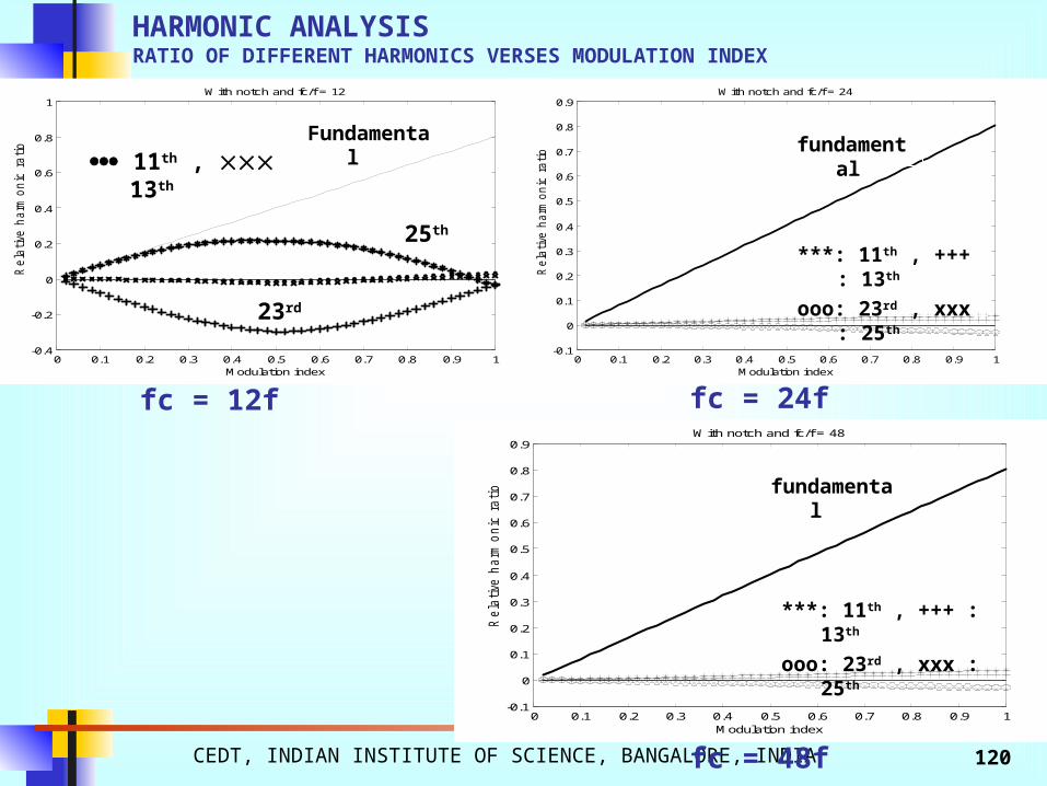
CEDT, INDIAN INSTITUTE OF SCIENCE, BANGALORE, INDIA 120
0 0.1 0.2 0.3 0.4 0.5 0.6 0.7 0.8 0.9 1-0.4
-0.2
0
0.2
0.4
0.6
0.8
1With notch and fc/f = 12
Modulation index
Rela
tive
harm
onic
ratio
Fundamental
25th
23rd
11th , 13th
0 0.1 0.2 0.3 0.4 0.5 0.6 0.7 0.8 0.9 1-0.1
0
0.1
0.2
0.3
0.4
0.5
0.6
0.7
0.8
0.9With notch and fc/f = 24
Modulation index
Rela
tive
harm
onic
ratio fundamental
***: 11th , +++ : 13th
ooo: 23rd , xxx : 25th
fc = 12f fc = 24f
0 0.1 0.2 0.3 0.4 0.5 0.6 0.7 0.8 0.9 1-0.1
0
0.1
0.2
0.3
0.4
0.5
0.6
0.7
0.8
0.9With notch and fc/f = 48
Modulation index
Rela
tive
harm
onic
ratio fundamental
***: 11th , +++ : 13th
ooo: 23rd , xxx : 25th
fc = 48f
HARMONIC ANALYSISRATIO OF DIFFERENT HARMONICS VERSES MODULATION INDEX
A Novel Modulation Scheme for a Six Phase Induction Motor with Open-End Windings

CEDT, INDIAN INSTITUTE OF SCIENCE, BANGALORE, INDIA 122
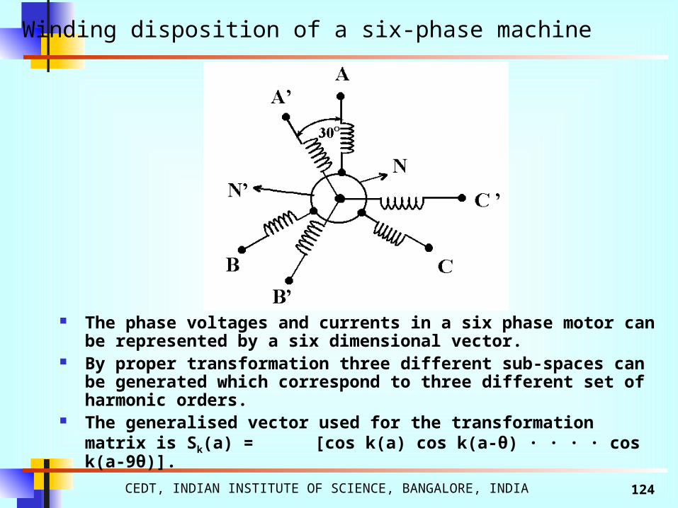
Six phase (split phase)motor configuration is achieved by splitting the phase belt of a conventional 3-phase induction motor into two halves namely abc and a’b’c’.
The phase separation between a and a’, b and b’ and c and c’ is 30°
Winding disposition of a six-phase machine

CEDT, INDIAN INSTITUTE OF SCIENCE, BANGALORE, INDIA 123
For a six phase induction motor drive harmonics of the order 6n 1( n=1,3,5 etc.,) will not contribute to the air gap flux.
All these 6n 1 ( n=1,3,5 etc.,) order harmonic currents are limited by the stator impedance only and hence contribute to large harmonic currents.
Inverter fed six-phase IM drive
CEDT, INDIAN INSTITUTE OF SCIENCE, BANGALORE, INDIA 124
The phase voltages and currents in a six phase motor can be represented by a six dimensional vector.
By proper transformation three different sub-spaces can be generated which correspond to three different set of harmonic orders.
The generalised vector used for the transformation matrix is Sk(a) = [cos k(a) cos k(a-θ) · · · · cos k(a-9θ)].
Winding disposition of a six-phase machine

CEDT, INDIAN INSTITUTE OF SCIENCE, BANGALORE, INDIA 125
By putting a = 0 and π/2, and θ equals to multiples of 30º in the generalised vector a transformation matrix is obtained.
θ = angular space separation between the two sets of 3-phase windings.

CEDT, INDIAN INSTITUTE OF SCIENCE, BANGALORE, INDIA 126
The harmonics of order 6n1 ( n = 0, 2,4 etc.,) span a 2-dimesional subspace ‘s1’.
The harmonics of order 6n1 ( n = 1, 3,5 etc.,) span a 2-dimesional subspace ‘s2’.
The triplen order harmonics span a 2-dimesional subspace ‘s3’.
They are orthogonal to each other.

CEDT, INDIAN INSTITUTE OF SCIENCE, BANGALORE, INDIA 127
All switching vectors projected on subspace‘S1’ generates 6n1 ( n = 0, 2,4 etc.,) harmonics.
Switching vectors in sub-space ‘S1’
CEDT, INDIAN INSTITUTE OF SCIENCE, BANGALORE, INDIA 128
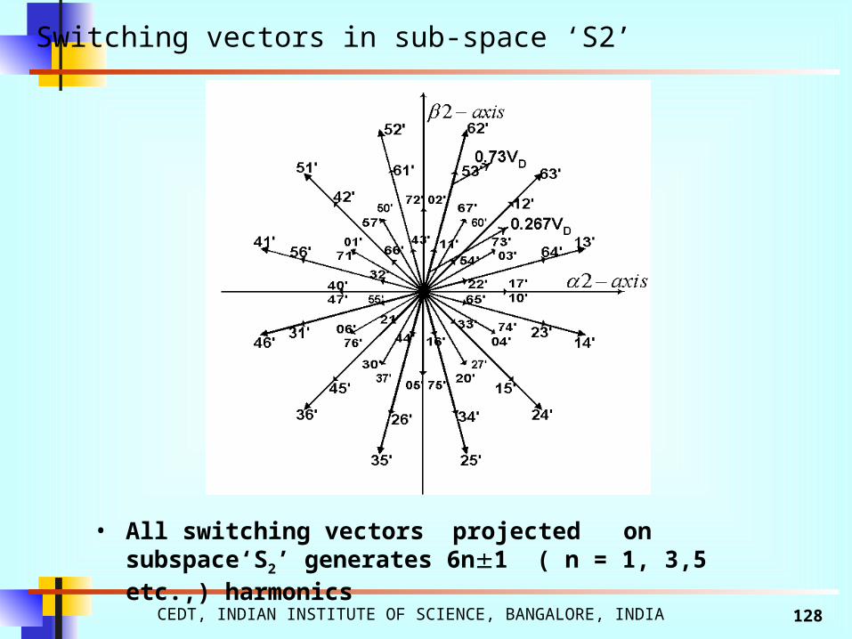
• All switching vectors projected on subspace‘S2’ generates 6n1 ( n = 1, 3,5 etc.,) harmonics
Switching vectors in sub-space ‘S2’
CEDT, INDIAN INSTITUTE OF SCIENCE, BANGALORE, INDIA 129
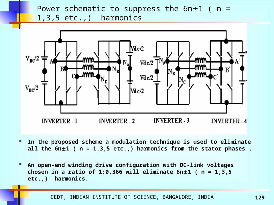
In the proposed scheme a modulation technique is used to eliminate all the 6n1 ( n = 1,3,5 etc.,) harmonics from the stator phases .
An open-end winding drive configuration with DC-link voltages chosen in a ratio of 1:0.366 will eliminate 6n1 ( n = 1,3,5 etc.,) harmonics.
Power schematic to suppress the 6n1 ( n = 1,3,5 etc.,) harmonics

CEDT, INDIAN INSTITUTE OF SCIENCE, BANGALORE, INDIA 130
From one side of open-end winding (inverter-1 and inverter-4) 11’,21’, 22’,
32’,33’,43’,44’,54,,55’,65’,66’ and 16’ vectors are switched. From the opposite side (inverter-2 and inverter-3) vectors 53’,
45’, 64’, 56’, 15’, 61’, 26’, 12’, 31’, 23’, 42’, and 34’ are switched.
Inverter vector selection to suppress the 6n1 ( n = 1,3,5 etc.,) harmonics
CEDT, INDIAN INSTITUTE OF SCIENCE, BANGALORE, INDIA 131
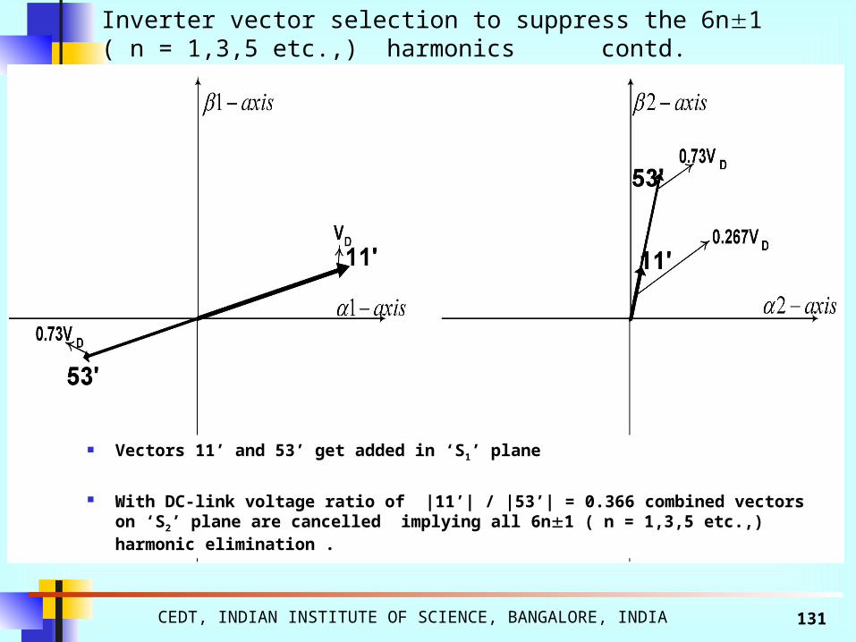
Vectors 11’ and 53’ get added in ‘S1’ plane
With DC-link voltage ratio of |11’| / |53’| = 0.366 combined vectors on ‘S2’ plane are cancelled implying all 6n1 ( n = 1,3,5 etc.,) harmonic elimination .
Inverter vector selection to suppress the 6n1 ( n = 1,3,5 etc.,) harmonics contd.

CEDT, INDIAN INSTITUTE OF SCIENCE, BANGALORE, INDIA 132
With DC-link voltage ratio of 0.366 12-sided polygonal voltage space phasor combinations are achieved for each 3-phase groups independently.
A modulation scheme based on 12-sided polygonal voltage space phasors will cancel the 6n1 ( n = 1,3,5 etc.,) harmonics voltage from all the motor phases.

CEDT, INDIAN INSTITUTE OF SCIENCE, BANGALORE, INDIA 133
Phase voltage
Harmonic spectrum
Phase currents.
6n1 ( n = 1,3,5 etc.,) harmonics are absent.
Experimental results
CEDT, INDIAN INSTITUTE OF SCIENCE, BANGALORE, INDIA 134
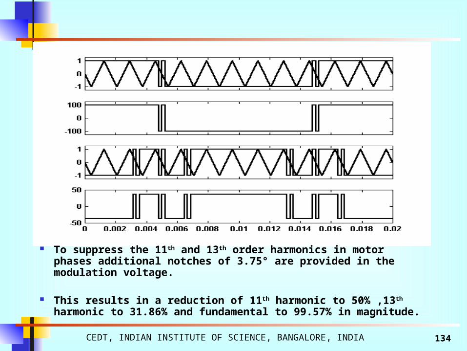
To suppress the 11th and 13th order harmonics in motor phases additional notches of 3.75° are provided in the modulation voltage.
This results in a reduction of 11th harmonic to 50% ,13th harmonic to 31.86% and fundamental to 99.57% in magnitude.
CEDT, INDIAN INSTITUTE OF SCIENCE, BANGALORE, INDIA 135
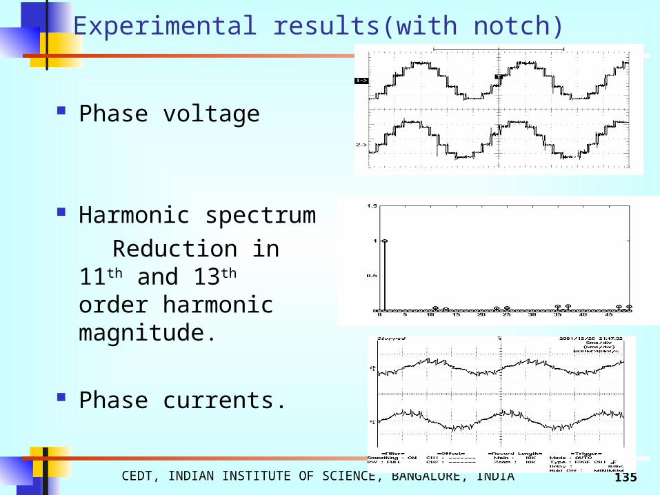
Experimental results(with notch)
Phase voltage
Harmonic spectrum Reduction in 11th
and 13th order harmonic magnitude.
Phase currents.

CEDT, INDIAN INSTITUTE OF SCIENCE, BANGALORE, INDIA 136
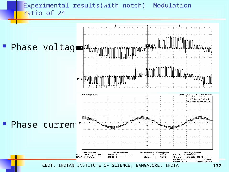
Experimental results(with notch) Modulation ratio of 12.
Phase voltage
Phase currents
CEDT, INDIAN INSTITUTE OF SCIENCE, BANGALORE, INDIA 137
Experimental results(with notch) Modulation ratio of 24
Phase voltage
Phase currents
IA
CEDT, INDIAN INSTITUTE OF SCIENCE, BANGALORE, INDIA 138
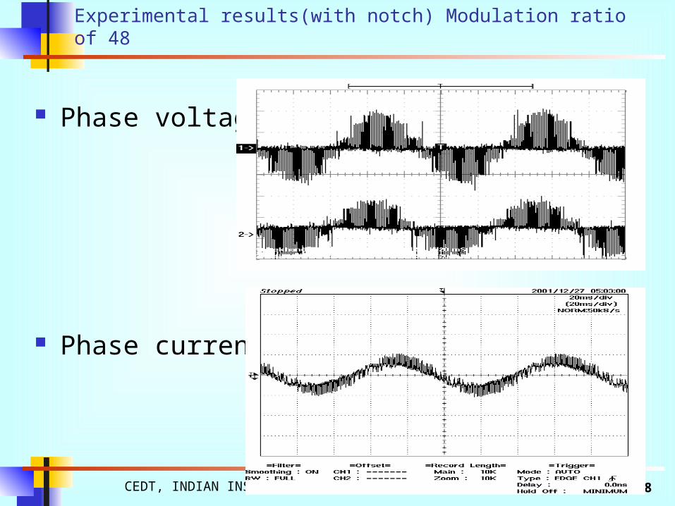
Experimental results(with notch) Modulation ratio of 48
Phase voltage
Phase currents
CEDT, INDIAN INSTITUTE OF SCIENCE, BANGALORE, INDIA 139
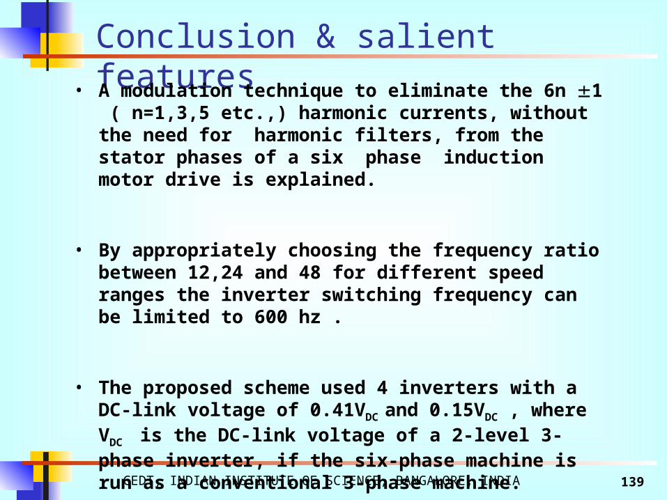
Conclusion & salient features• A modulation technique to eliminate the 6n 1 ( n=1,3,5 etc.,)
harmonic currents, without the need for harmonic filters, from the stator phases of a six phase induction motor drive is explained.
• By appropriately choosing the frequency ratio between 12,24 and 48 for different speed ranges the inverter switching frequency can be limited to 600 hz .
• The proposed scheme used 4 inverters with a DC-link voltage of 0.41VDC and 0.15VDC , where VDC
is the DC-link voltage of a 2-level 3-phase inverter, if the six-phase machine is run as a conventional 3-phase machine.
INDEPENDENT SPEED CONTROL OF TWO SIX PHASE INDUCTION MOTORS USING A SINGLE SIX PHASE INVERTER
CEDT, INDIAN INSTITUTE OF SCIENCE, BANGALORE, INDIA 141
A method of independent speed control of two induction motors from a single six-phase inverter is proposed.
The positive sequence component consists of all the 12n 1 (n = 0,1,2, ….etc.) order harmonics.
One of the two zero sequence components consists of all the 6n 1 (n = 1,3,5 ….etc.) order harmonics .
Introduction
CEDT, INDIAN INSTITUTE OF SCIENCE, BANGALORE, INDIA 142
30˚
INVERTER – 2 INVERTER - 1
AVDC/2
NN’ C ’
CB’B
A’A
A’
B’o BCVDC/2
C’
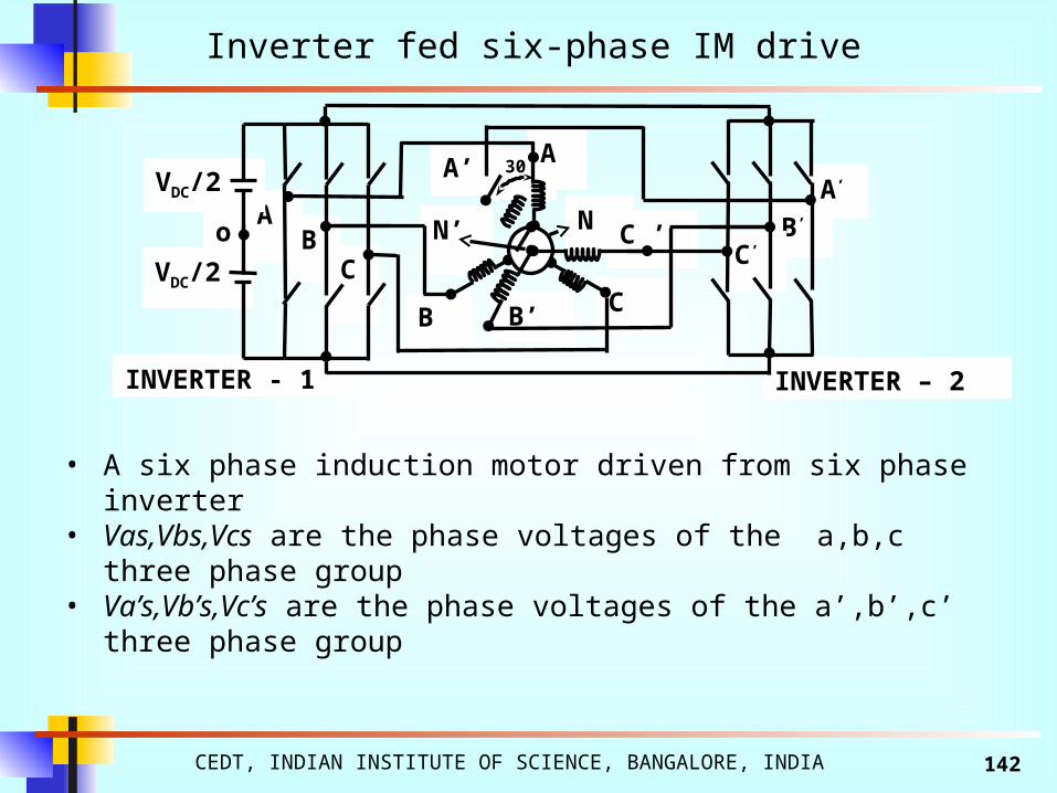
• A six phase induction motor driven from six phase inverter• Vas,Vbs,Vcs are the phase voltages of the a,b,c three
phase group• Va’s,Vb’s,Vc’s are the phase voltages of the a’,b’,c’ three
phase group
Inverter fed six-phase IM drive

CEDT, INDIAN INSTITUTE OF SCIENCE, BANGALORE, INDIA 143
s'Vc
Vcs
s'Vb
Vbs
s'Va
Vas
101010
010101
9sin4sinsin8sin5sin0
9cos4coscos8cos5cos1
9sin8sin5sin4sinsin0
9cos8cos5cos4coscos1
)3/1(
2V
1V
2V
1V
V
V
• Vas, Vbs, Vcs for a,b,c group.• Va’s, Vb’s, Vc’s for a’,b’,c’ group.
• Vα, Vβ … Harmonics spanning subspace S1 [12n 1 (n = 0,1,2,3 ….etc.,)]
• V1, V2 … Harmonics spanning subspace S2
[6n 1 (n = 1,3,5 order ….etc.,)]
• Vo1, Vo2… Harmonics spanning subspace S3 [triplen harmonic ]

CEDT, INDIAN INSTITUTE OF SCIENCE, BANGALORE, INDIA 144
risrLsissLdt
dsisRVs
Stator Voltage equation
Vs is input voltage vectors, si is input stator current vectors,
is input stator current vectors, ri
sR is stator resistance matrix, ssL is stator self inductance matrix,
srL is stator to rotor mutual inductance matrix.
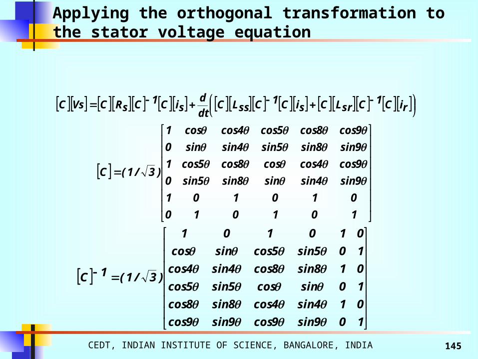
CEDT, INDIAN INSTITUTE OF SCIENCE, BANGALORE, INDIA 145
riC1CsrLCsiC1CssLC
dt
dsiC1CsRCVsC
101010
010101
9sin4sinsin8sin5sin0
9cos4coscos8cos5cos1
9sin8sin5sin4sinsin0
9cos8cos5cos4coscos1
)3/1(C
109sin9cos9sin9cos
014sin4cos8sin8cos
10sincos5sin5cos
018sin8cos4sin4cos
105sin5cossincos
010101
)3/1(1C
Applying the orthogonal transformation to the stator voltage equation

CEDT, INDIAN INSTITUTE OF SCIENCE, BANGALORE, INDIA 146
r2ir1iriri
.
0000
0000
00)rcos(M3)rsin(M3
00)rsin(M3)rcos(M3
dt
d
s2is1isisi
.
lsL000
0lsL00
00M3lsL0
000M3lsL
dt
d
s2is1isisi
44sR
2V1V
V
V
si,si are two orthogonal components of stator currents spanning subspace S1 ,
s2i,s1i are two orthogonal components of stator currents spanning subspace S2 ,
ri,ri are the two orthogonal components of rotor currents spanning subspace S1 ,
r2i,r1i are two orthogonal components of rotor currents spanning subspace S2 .

CEDT, INDIAN INSTITUTE OF SCIENCE, BANGALORE, INDIA 147
Rotor voltage equation
si.rsLri.rrLdt
dri.Rr0
rR is stator resistance matrix, rrL is stator self inductance matrix,
rsL is rotor to stator mutual inductance matrix.

CEDT, INDIAN INSTITUTE OF SCIENCE, BANGALORE, INDIA 148
si.C1C.rsL.Cri.C1C.rrL.C
dt
dri.C1C.rR.C0
• By applying the orthogonal transformation to the rotor voltage equation
s2is1isisi
.
0000
0000
00)rcos(M3)rsin(M3
00)rsin(M3)rcos(M3
dt
d
r2ir1iriri
.
lrL000
0lrL00
00M3lrL0
000M3lrL
dt
d
r2ir1iriri
44rR
0
0
0
0

CEDT, INDIAN INSTITUTE OF SCIENCE, BANGALORE, INDIA 149
• The corresponding voltage equations of stator and rotor spanning subspaces S1 and S2 can be separated out
ririsisi
.
M3lrL0)rcos(M3)rsin(M3
0M3lrL)rsin(M3)rcos(M3
)rcos(M3)rsin(M3M3lsL0
)rsin(M3)rcos(M30M3lsL
dt
d
ririsisi
rR000
0rR00
00sR0
000sR
0
0
V
V
r2ir1is2is1i
.
lrL000
0lrL00
00lsL0
000lsL
dt
d
r2ir1is2is1i
rR000
0rR00
00sR0
000sR
0
02V1V
Subspaces S1 ….
Subspaces S2 ….

CEDT, INDIAN INSTITUTE OF SCIENCE, BANGALORE, INDIA 150
•Only the positive sequence components traversing subspace S1 contribute for the air gap flux and electromagnetic torque production in machine.
•The zero sequence components do not contribute towards air gap flux production with the existing winding
disposition.
CEDT, INDIAN INSTITUTE OF SCIENCE, BANGALORE, INDIA 151
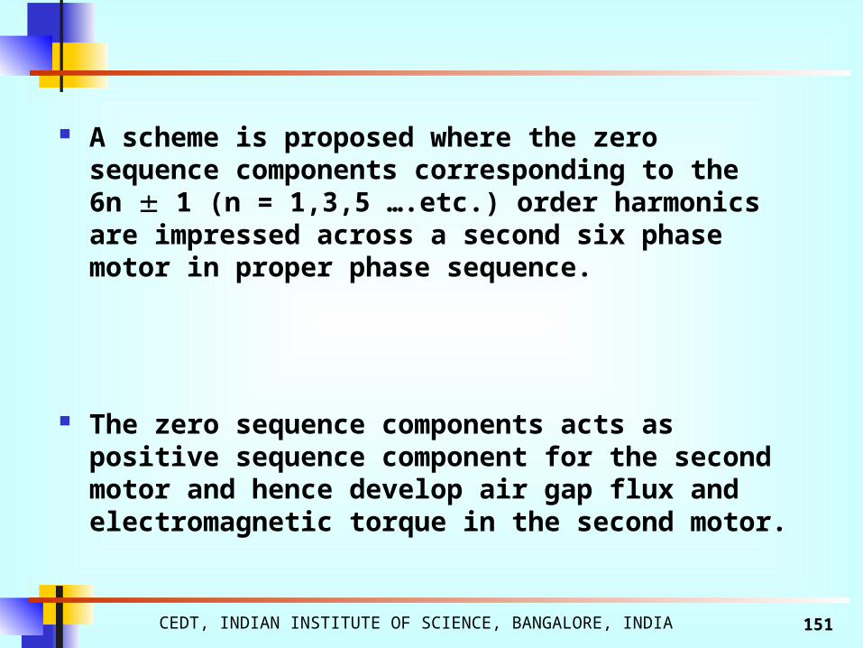
A scheme is proposed where the zero sequence components corresponding to the 6n 1 (n = 1,3,5 ….etc.) order harmonics are impressed across a second six phase motor in proper phase sequence.
The zero sequence components acts as positive sequence component for the second motor and hence develop air gap flux and electromagnetic torque in the second motor.

CEDT, INDIAN INSTITUTE OF SCIENCE, BANGALORE, INDIA 152
B’
180˚ +30˚
N
N’C ’
C
B
A’
A
Stator schematic of the reconfigured six phase induction machine ( voltage components in the S2 plane create air gap flux and torque)
Six-phase IM winding disposition:-S2 subspace components produce torque
CEDT, INDIAN INSTITUTE OF SCIENCE, BANGALORE, INDIA 153
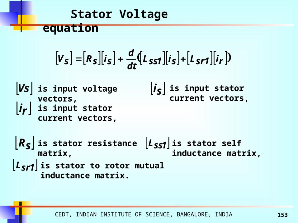
ri1srLsi1ssLdt
dsisRsV
Stator Voltage equation
Vs is input voltage vectors, si is input stator current vectors,
is input stator current vectors, ri
sR is stator resistance matrix, 1ssL is stator self inductance matrix,
1srL is stator to rotor mutual inductance matrix.
CEDT, INDIAN INSTITUTE OF SCIENCE, BANGALORE, INDIA 154
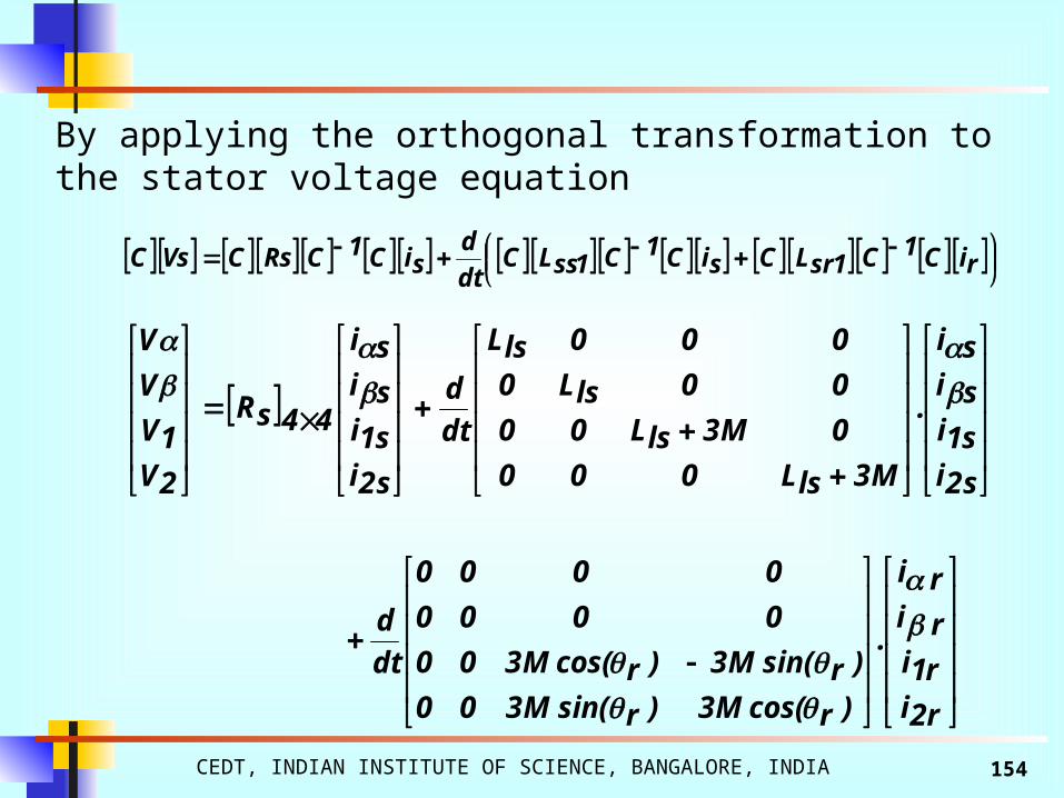
riC1C1srLCsiC1C1ssLC
dt
dsiC1CRsCVsC
By applying the orthogonal transformation to the stator voltage equation
r2ir1iriri
.
)rcos(M3)rsin(M300
)rsin(M3)rcos(M300
0000
0000
dt
d
s2is1isisi
.
M3lsL000
0M3lsL00
00lsL0
000lsL
dt
d
s2is1isisi
44sR
2V1V
V
V

CEDT, INDIAN INSTITUTE OF SCIENCE, BANGALORE, INDIA 155
si.1rsLri.1rrLdt
dri.Rr0
Rotor Voltage equation
rR is stator resistance matrix, 1rrL is stator self inductance matrix,
1rsL is rotor to stator mutual inductance matrix.

CEDT, INDIAN INSTITUTE OF SCIENCE, BANGALORE, INDIA 156
siC1C1rsLCriC1C1rrLC
dt
driC1CrRC0
• By applying the orthogonal transformation to the rotor voltage equation
s2is1isisi
.
)rcos(M3)rsin(M300
)rsin(M3)rcos(M300
0000
0000
dt
d
r2ir1iriri
.
M3lrL000
0M3lrL00
00lrL0
000lrL
dt
d
r2ir1iriri
44rR
0
0
0
0

CEDT, INDIAN INSTITUTE OF SCIENCE, BANGALORE, INDIA 157
• The corresponding voltage equations of stator and rotor spanning subspaces S1 and S2 can be separated out
Subspaces S1 ….
Subspaces S2 ….
ririsisi
.
lrL000
0lrL00
00lsL0
000lsL
dt
d
ririsisi
rR000
0rR00
00sR0
000sR
0
0
V
V
r2ir1is2is1i
.
M3lrL0)rcos(M3)rsin(M3
0M3lrL)rsin(M3)rcos(M3
)rcos(M3)rsin(M3M3lsL0
)rsin(M3)rcos(M30M3lsL
dt
d
r2ir1is2is1i
rR000
0rR00
00sR0
000sR
0
02V1V
CEDT, INDIAN INSTITUTE OF SCIENCE, BANGALORE, INDIA 158
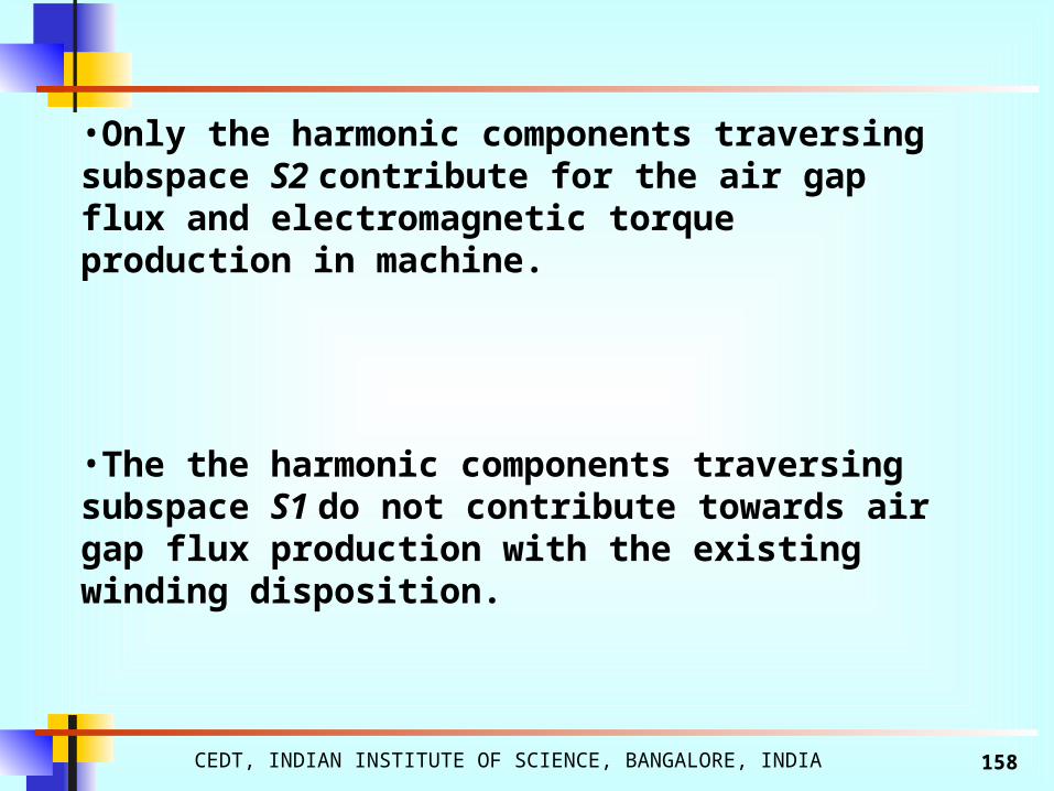
•Only the harmonic components traversing subspace S2 contribute for the air gap flux and electromagnetic torque production in machine.
•The the harmonic components traversing subspace S1 do not contribute towards air gap flux production with the existing winding disposition.
CEDT, INDIAN INSTITUTE OF SCIENCE, BANGALORE, INDIA 159
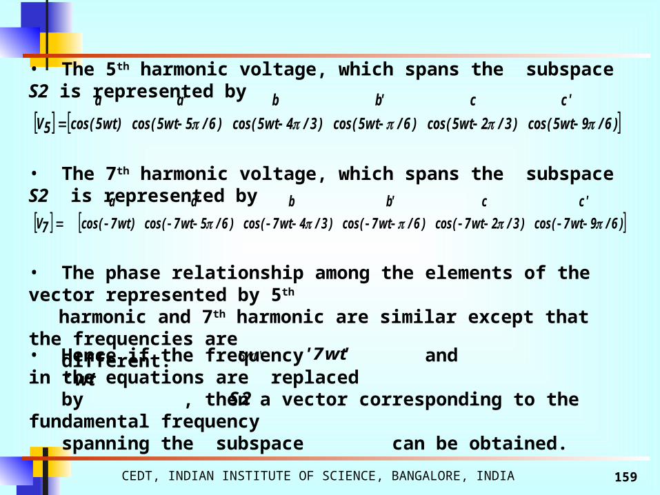
)6/9wt5(cos)3/2wt5(cos)6/wt5(cos)3/4wt5(cos)6/5wt5(cos)wt5(cos5V
'cc'bb'aa
)6/9wt7(cos)3/2wt7(cos)6/wt7(cos)3/4wt7(cos)6/5wt7(cos)wt7(cos7V
'cc'bb'aa
• The 5th harmonic voltage, which spans the subspace S2 is represented by
• The 7th harmonic voltage, which spans the subspace S2 is represented by
• The phase relationship among the elements of the vector represented by 5th
harmonic and 7th harmonic are similar except that the frequencies are different.
• Hence if the frequency and in the equations are replaced by , then a vector corresponding to the fundamental frequency spanning the subspace can be obtained.
'5' wt 'wt7'
'wt'2S
CEDT, INDIAN INSTITUTE OF SCIENCE, BANGALORE, INDIA 160
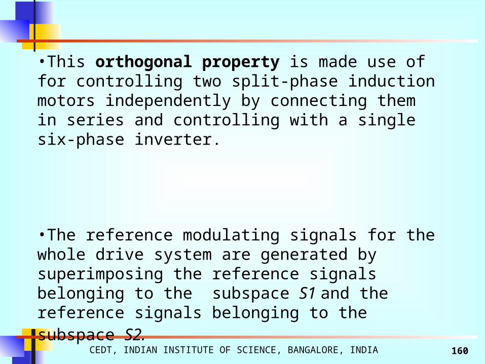
•This orthogonal property is made use of for controlling two split-phase induction motors independently by connecting them in series and controlling with a single six-phase inverter.
•The reference modulating signals for the whole drive system are generated by superimposing the reference signals belonging to the subspace S1 and the reference signals belonging to the subspace S2.

CEDT, INDIAN INSTITUTE OF SCIENCE, BANGALORE, INDIA 161
30˚
N2
N2
N2
A2B2’
C2’
C2 B2
A2’
C1’
C1
B1’
B1
A1’A1
MACHINE-1( 2-pole 2kw)
MACHINE-2( 4-pole 1kw)
180˚ +30˚
N’
Schematic of the stator phase windings of the two series connected six phase induction motors
CEDT, INDIAN INSTITUTE OF SCIENCE, BANGALORE, INDIA 162
0
0
0
0
V
V
1C
1s'Vc
1Vcs
1s'Vb
1Vbs
1s'Va
1Vas
0
0
2V
1V
0
0
1C
2s'Vc
2Vcs
2s'Vb
2Vbs
2s'Va
2Vas
2s'Vc1s'Vc
2Vcs1Vcs
2s'Vb1s'Vb
2Vbs1Vbs
2s'Va1s'Va
2Vas1Vas
s'Vc
Vcs
s'Vb
Vbs
s'Va
Vas
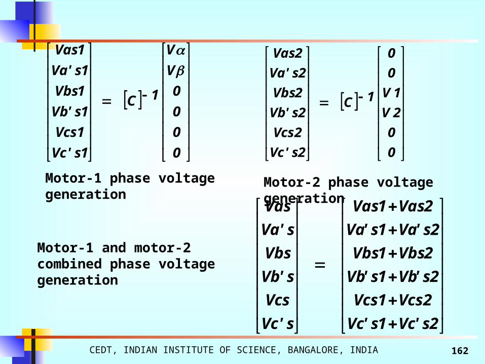
Motor-1 phase voltage generation
Motor-1 and motor-2 combined phase voltage generation
Motor-2 phase voltage generation
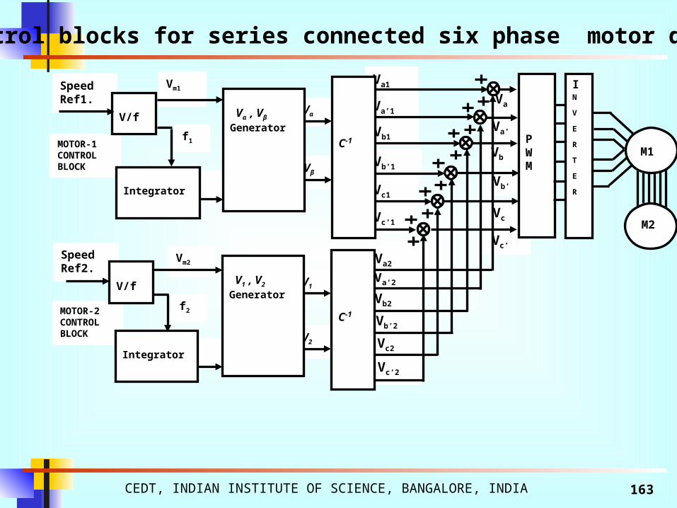
CEDT, INDIAN INSTITUTE OF SCIENCE, BANGALORE, INDIA 163
MOTOR-1 CONTROL BLOCK
MOTOR-2 CONTROLBLOCK
Integrator
Vc2
Vc’2
Vb2
Va’2
SpeedRef2.
SpeedRef1.
Va2
Vc’
Vc
Vb’
Vb
Va’
Va
Vb’2
Vc’1
Vc1
Vb’1
Vb1
Va’1
Va1
Vβ
Vα
Vm1
V/f
Integrator
Vα , Vβ Generator C-1
V2
V1
Vm2
V1 , V2 Generator
C-1
PWM
IN
V
E
R
T
E
R
M1
M2
V/f
f1
f2
Control blocks for series connected six phase motor drive
CEDT, INDIAN INSTITUTE OF SCIENCE, BANGALORE, INDIA 164
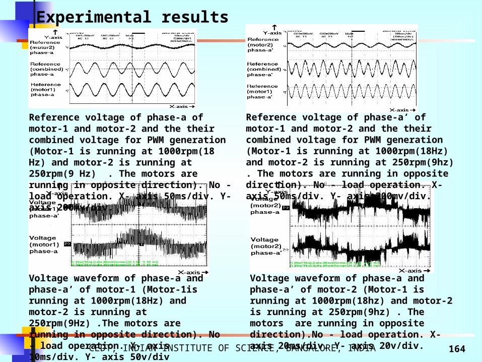
Voltage waveform of phase-a and phase-a’ of motor-2 (Motor-1 is running at 1000rpm(18hz) and motor-2 is running at 250rpm(9hz) . The motors are running in opposite direction).No - load operation. X- axis 20ms/div. Y- axis 20v/div.
Voltage waveform of phase-a and phase-a’ of motor-1 (Motor-1is running at 1000rpm(18Hz) and motor-2 is running at 250rpm(9Hz) .The motors are running in opposite direction). No - load operation. X- axis 10ms/div. Y- axis 50v/div
Reference voltage of phase-a’ of motor-1 and motor-2 and the their combined voltage for PWM generation (Motor-1 is running at 1000rpm(18Hz) and motor-2 is running at 250rpm(9hz) . The motors are running in opposite direction). No - load operation. X- axis 50ms/div. Y- axis 200mv/div.
Reference voltage of phase-a of motor-1 and motor-2 and the their combined voltage for PWM generation (Motor-1 is running at 1000rpm(18 Hz) and motor-2 is running at 250rpm(9 Hz) . The motors are running in opposite direction). No - load operation. X- axis 50ms/div. Y- axis 200mv/div.
Experimental results
CEDT, INDIAN INSTITUTE OF SCIENCE, BANGALORE, INDIA 165
0 10 20 30 40 500
0.2
0.4
0.6
0.8
1
RELATIVE AMPLITUDES OF DIFFERENT FREQUENCY COMPONENTS IN PHASE CURRENT
NORMALISED FREQUENCY
RE
LA
TIV
E A
MP
LIT
UD
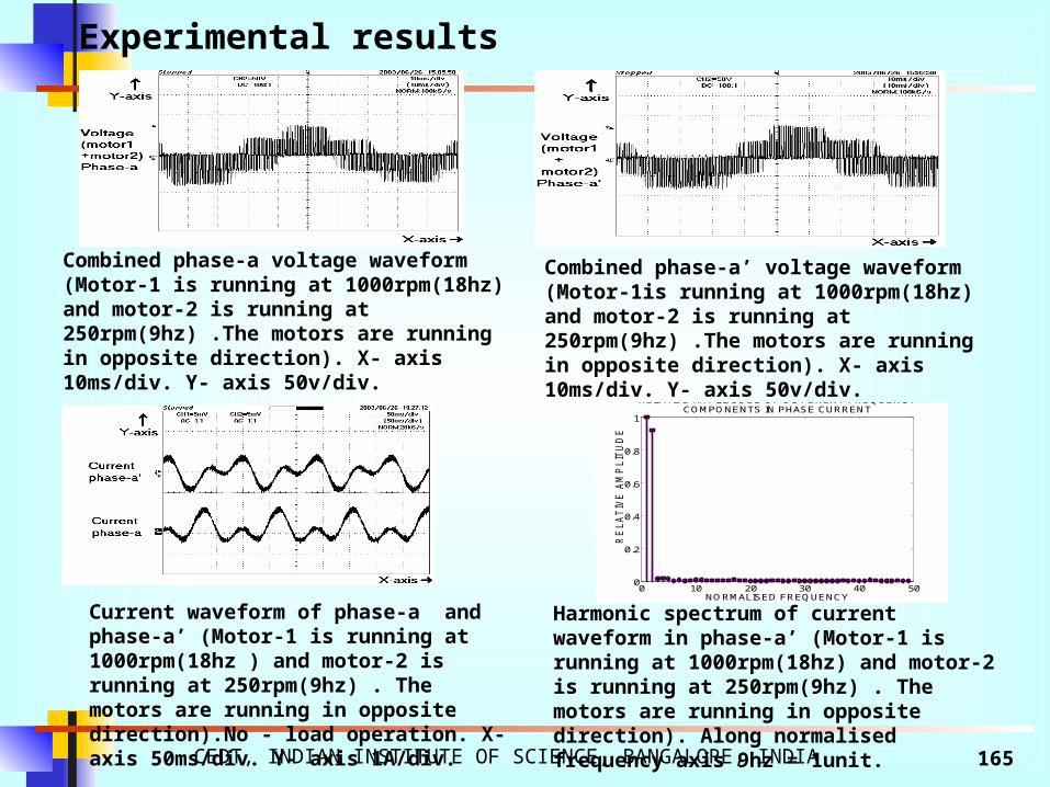
EHarmonic spectrum of current waveform in phase-a’ (Motor-1 is running at 1000rpm(18hz) and motor-2 is running at 250rpm(9hz) . The motors are running in opposite direction). Along normalised frequency axis 9hz = 1unit.
Current waveform of phase-a and phase-a’ (Motor-1 is running at 1000rpm(18hz ) and motor-2 is running at 250rpm(9hz) . The motors are running in opposite direction).No - load operation. X- axis 50ms/div. Y- axis 1A/div.
Combined phase-a’ voltage waveform (Motor-1is running at 1000rpm(18hz) and motor-2 is running at 250rpm(9hz) .The motors are running in opposite direction). X- axis 10ms/div. Y- axis 50v/div.
Combined phase-a voltage waveform (Motor-1 is running at 1000rpm(18hz) and motor-2 is running at 250rpm(9hz) .The motors are running in opposite direction). X- axis 10ms/div. Y- axis 50v/div.
Experimental results
CEDT, INDIAN INSTITUTE OF SCIENCE, BANGALORE, INDIA 166
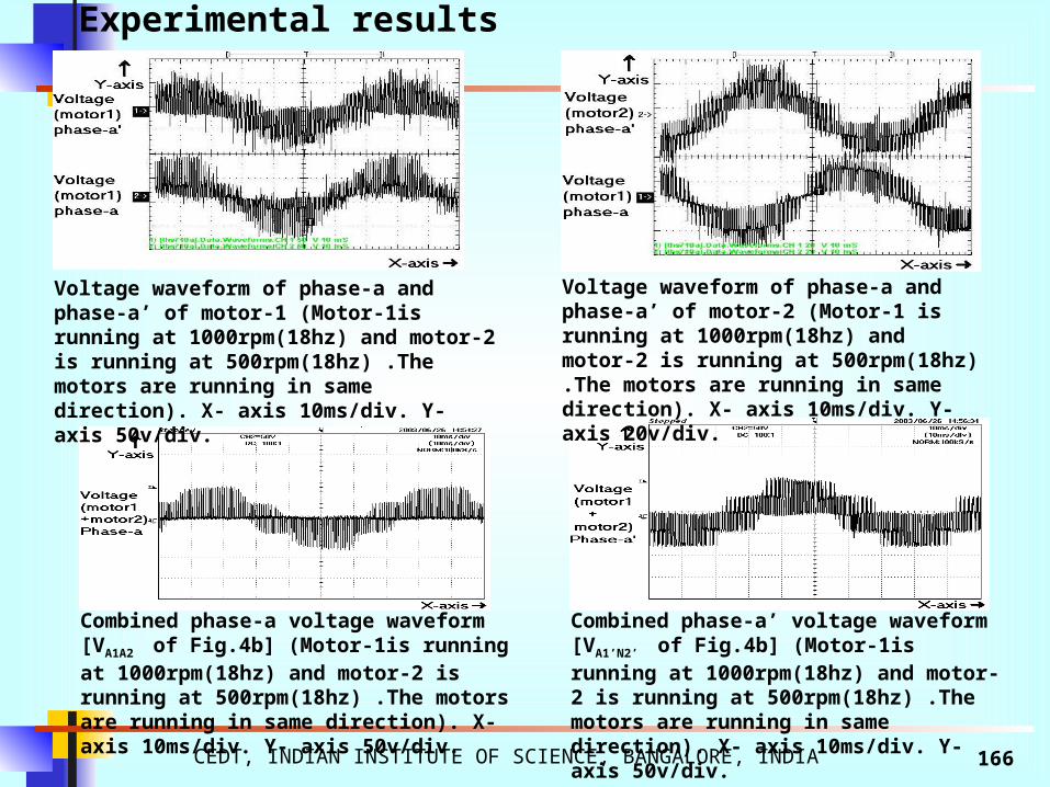
Combined phase-a’ voltage waveform [VA1’N2’ of Fig.4b] (Motor-1is running at 1000rpm(18hz) and motor-2 is running at 500rpm(18hz) .The motors are running in same direction). X- axis 10ms/div. Y- axis 50v/div.
Combined phase-a voltage waveform [VA1A2 of Fig.4b] (Motor-1is running at 1000rpm(18hz) and motor-2 is running at 500rpm(18hz) .The motors are running in same direction). X- axis 10ms/div. Y- axis 50v/div.
Voltage waveform of phase-a and phase-a’ of motor-2 (Motor-1 is running at 1000rpm(18hz) and motor-2 is running at 500rpm(18hz) .The motors are running in same direction). X- axis 10ms/div. Y- axis 20v/div.
Voltage waveform of phase-a and phase-a’ of motor-1 (Motor-1is running at 1000rpm(18hz) and motor-2 is running at 500rpm(18hz) .The motors are running in same direction). X- axis 10ms/div. Y- axis 50v/div.
Experimental results
CEDT, INDIAN INSTITUTE OF SCIENCE, BANGALORE, INDIA 167
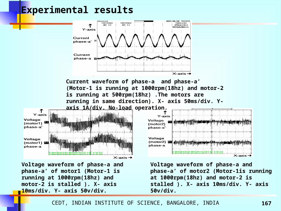
Voltage waveform of phase-a and phase-a’ of motor1 (Motor-1 is running at 1000rpm(18hz) and motor-2 is stalled ). X- axis 10ms/div. Y- axis 50v/div.
Voltage waveform of phase-a and phase-a’ of motor2 (Motor-1is running at 1000rpm(18hz) and motor-2 is stalled ). X- axis 10ms/div. Y- axis 50v/div.
Current waveform of phase-a and phase-a’ (Motor-1 is running at 1000rpm(18hz) and motor-2 is running at 500rpm(18hz) .The motors are running in same direction). X- axis 50ms/div. Y- axis 1A/div. No-load operation.
Experimental results
CEDT, INDIAN INSTITUTE OF SCIENCE, BANGALORE, INDIA 168
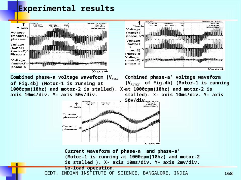
Current waveform of phase-a and phase-a’ (Motor-1 is running at 1000rpm(18hz) and motor-2 is stalled ). X- axis 10ms/div. Y- axis 2mv/div. No-load operation.
Combined phase-a voltage waveform [VA1A2 of Fig.4b] (Motor-1 is running at 1000rpm(18hz) and motor-2 is stalled). X- axis 10ms/div. Y- axis 50v/div.
Combined phase-a’ voltage waveform [VA1’N2’ of Fig.4b] (Motor-1 is running at 1000rpm(18hz) and motor-2 is stalled). X- axis 10ms/div. Y- axis 50v/div.
Experimental results
CEDT, INDIAN INSTITUTE OF SCIENCE, BANGALORE, INDIA 169
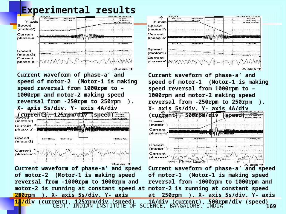
Current waveform of phase-a’ and speed of motor-2 (Motor-1 is making speed reversal from -1000rpm to 1000rpm and motor-2 is running at constant speed at 250rpm ). X- axis 5s/div. Y- axis 1A/div (current), 125rpm/div (speed)
Current waveform of phase-a’ and speed of motor-1 (Motor-1 is making speed reversal from -1000rpm to 1000rpm and motor-2 is running at constant speed at 250rpm ). X- axis 5s/div. Y- axis 1A/div (current), 500rpm/div (speed)
Current waveform of phase-a’ and speed of motor-2 (Motor-1 is making speed reversal from 1000rpm to –1000rpm and motor-2 making speed reversal from -250rpm to 250rpm ). X- axis 5s/div. Y- axis 4A/div (current), 125rpm/div (speed)
Current waveform of phase-a’ and speed of motor-1 (Motor-1 is making speed reversal from 1000rpm to –1000rpm and motor-2 making speed reversal from -250rpm to 250rpm ). X- axis 5s/div. Y- axis 4A/div (current), 500rpm/div (speed)
Experimental results
CEDT, INDIAN INSTITUTE OF SCIENCE, BANGALORE, INDIA 170
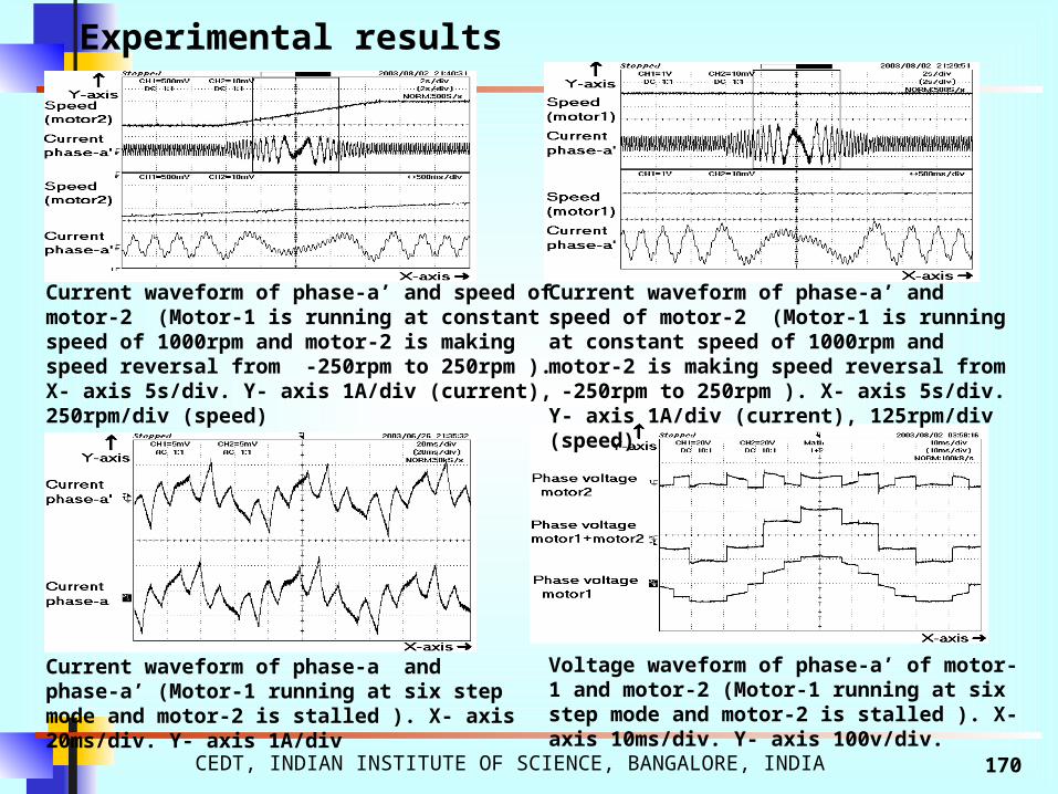
Current waveform of phase-a’ and speed of motor-2 (Motor-1 is running at constant speed of 1000rpm and motor-2 is making speed reversal from -250rpm to 250rpm ). X- axis 5s/div. Y- axis 1A/div (current), 250rpm/div (speed)
Current waveform of phase-a’ and speed of motor-2 (Motor-1 is running at constant speed of 1000rpm and motor-2 is making speed reversal from -250rpm to 250rpm ). X- axis 5s/div. Y- axis 1A/div (current), 125rpm/div (speed)
Current waveform of phase-a and phase-a’ (Motor-1 running at six step mode and motor-2 is stalled ). X- axis 20ms/div. Y- axis 1A/div
Voltage waveform of phase-a’ of motor-1 and motor-2 (Motor-1 running at six step mode and motor-2 is stalled ). X- axis 10ms/div. Y- axis 100v/div.
Experimental results

CEDT, INDIAN INSTITUTE OF SCIENCE, BANGALORE, INDIA 171
0 10 20 30 40 500
0.5
1
1.5
2
2.5
3x 10
5
NORMALISED FREQUENCY
RE
LA
TIV
E A
MP
LIT
UD
E
0 10 20 30 40 500
0.5
1
1.5
2
2.5
3
3.5x 10
4
NORMALISED FREQUENCY
RE
LA
TIV
E A
MP
LIT
UD
E
Harmonic spectrum of voltage waveform in phase-a’ of motor-1 (Motor-1 is running in over modulation (12 step) and motor-2 is stalled).
Harmonic spectrum of voltage waveform in phase-a’ of motor-2 (Motor-1 is running in over modulation (12 step) and motor-2 is stalled).
Current waveform of phase-a and phase-a’ (Motor-1 is stalled and motor-2 is running at six step mode). X- axis 20ms/div. Y- axis 1A/div
Voltage waveform of phase-a’ of motor-1 and motor-2 (Motor-1 is stalled and motor-2 is running at six step mode). X- axis 10ms/div. Y- axis 100v/div.
Experimental results

CEDT, INDIAN INSTITUTE OF SCIENCE, BANGALORE, INDIA 172
Conclusion & salient features• A de-coupled speed control of two split phase (six phase) induction motor, from a single six phase inverter system is presented.
• In normal six phase motor the phase voltages corresponding to the 6n 1 (n = 1,3,5 ….etc.,) harmonic orders do not create torque and air gap flux.
• But the phase voltages corresponding to the 6n 1(n = 1,3,5 ….etc.,) harmonic orders when applied to another six phase motor in proper phase sequence , torque and air gap flux are created.
• Thus by the proper series connections of phases of the two six phase motors, the two motors can be run independently from a single six phase inverter.
• Independent speed control of the two motors are possible without the need for costly and bulky harmonic filters to suppress the high amplitude 6n 1 (n = 1,3,5 ….etc.,) order zero sequence harmonic current components.
CEDT, INDIAN INSTITUTE OF SCIENCE, BANGALORE, INDIA 173
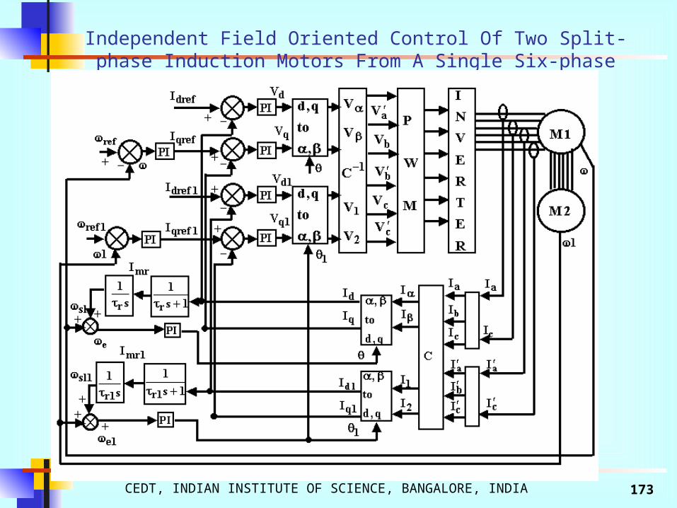
Independent Field Oriented Control Of Two Split-phase Induction Motors From A Single Six-phase Inverter
CEDT, INDIAN INSTITUTE OF SCIENCE, BANGALORE, INDIA 174
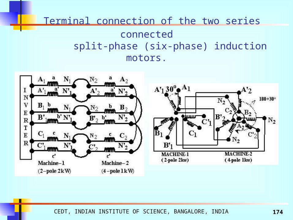
Terminal connection of the two series connected split-phase (six-phase) induction motors.
CEDT, INDIAN INSTITUTE OF SCIENCE, BANGALORE, INDIA 175
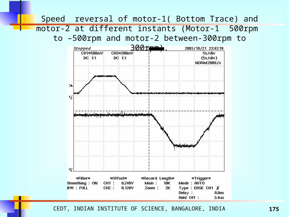
Speed reversal of motor-1( Bottom Trace) and motor-2 at different instants (Motor-1 500rpm to –500rpm and motor-2 between-300rpm to
300rpm).
CEDT, INDIAN INSTITUTE OF SCIENCE, BANGALORE, INDIA 176
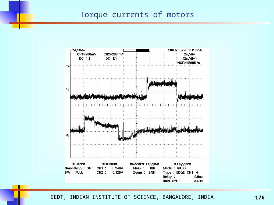
Torque currents of motors

CEDT, INDIAN INSTITUTE OF SCIENCE, BANGALORE, INDIA 177
simultaneous speed reversal of motors [( motor-1( Bottom trace) 500rpm to –500rpm and motor-2 ( Top Trace) -300rpm to 300rpm]

CEDT, INDIAN INSTITUTE OF SCIENCE, BANGALORE, INDIA 178
Torque currents of motor-1 ( Bottom Trace) and motor-2 (Top Trace)
CEDT, INDIAN INSTITUTE OF SCIENCE, BANGALORE, INDIA 179
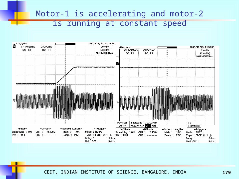
Motor-1 is accelerating and motor-2is running at constant speed

CEDT, INDIAN INSTITUTE OF SCIENCE, BANGALORE, INDIA 180
Motor-1 is doing speed reversal and Motor-2 is at constant speed operation

CEDT, INDIAN INSTITUTE OF SCIENCE, BANGALORE, INDIA 181

CEDT, INDIAN INSTITUTE OF SCIENCE, BANGALORE, INDIA 182
• Independent speed control of the two motors are possible without the need for costly and bulky harmonic filters to suppress the high amplitude 6n 1 (n = 1,3,5 ….etc.,) order zero sequence harmonic current components.

A SENSORLESS SPEED CONTROL FOR INDUCTION MOTORS USING RIPPLE CURRENTS IN SPACE PHASOR BASED PWM CONTROL

CEDT, INDIAN INSTITUTE OF SCIENCE, BANGALORE, INDIA 184
A new method to estimate speed of induction motor without shaft transducer is proposed.
The motor phase current ripple is used for estimation of rotor flux position.
Two different schemes are used for flux position estimation in two different regions, one in low speed region and the other in high speed region.
The proposed method uses space vector modulation with constant switching frequency.
Introduction
CEDT, INDIAN INSTITUTE OF SCIENCE, BANGALORE, INDIA 185
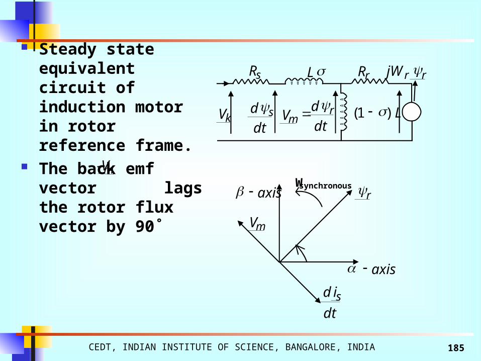
Steady state equivalent circuit of induction motor in rotor reference frame.
The back emf vector lags the rotor flux vector by 90˚
rR L
sR rrjW
kV L)1(
dt
d s
dt
dV r
m
Wsynchronous
dt
id s
mV
axis
axis r
m-V
CEDT, INDIAN INSTITUTE OF SCIENCE, BANGALORE, INDIA 186
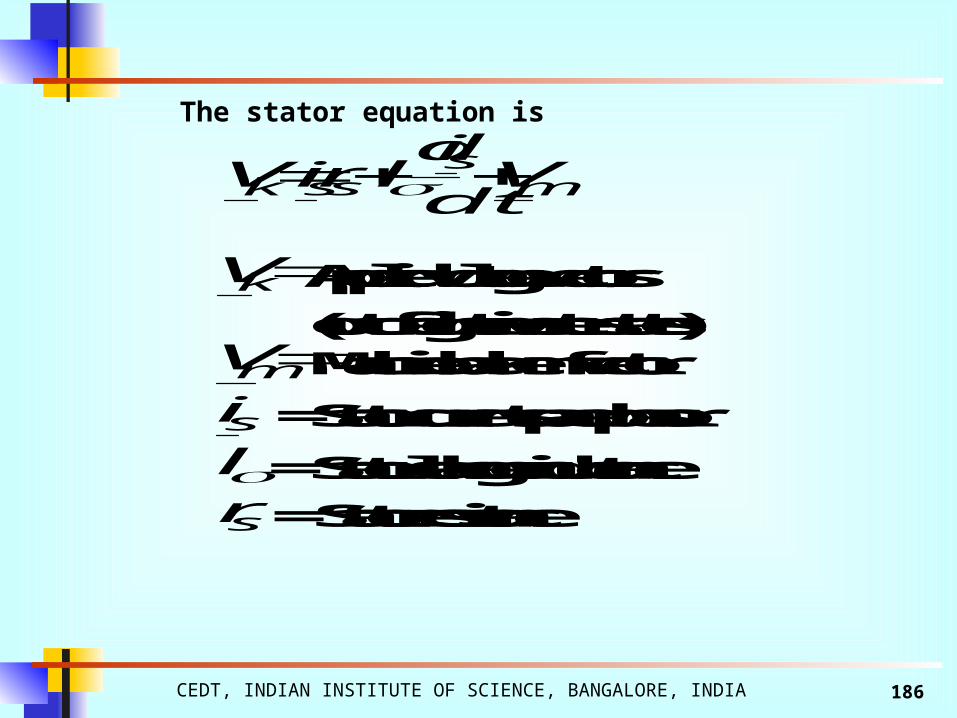
The stator equation is
ms
ssk Vdt
idlriV
kV Applied voltage vectors
(out of eight inverter states) mV Machine back emf vector
si = Stator current space phasor
l = Stator leakage inductance sr = Stator resistance
CEDT, INDIAN INSTITUTE OF SCIENCE, BANGALORE, INDIA 187
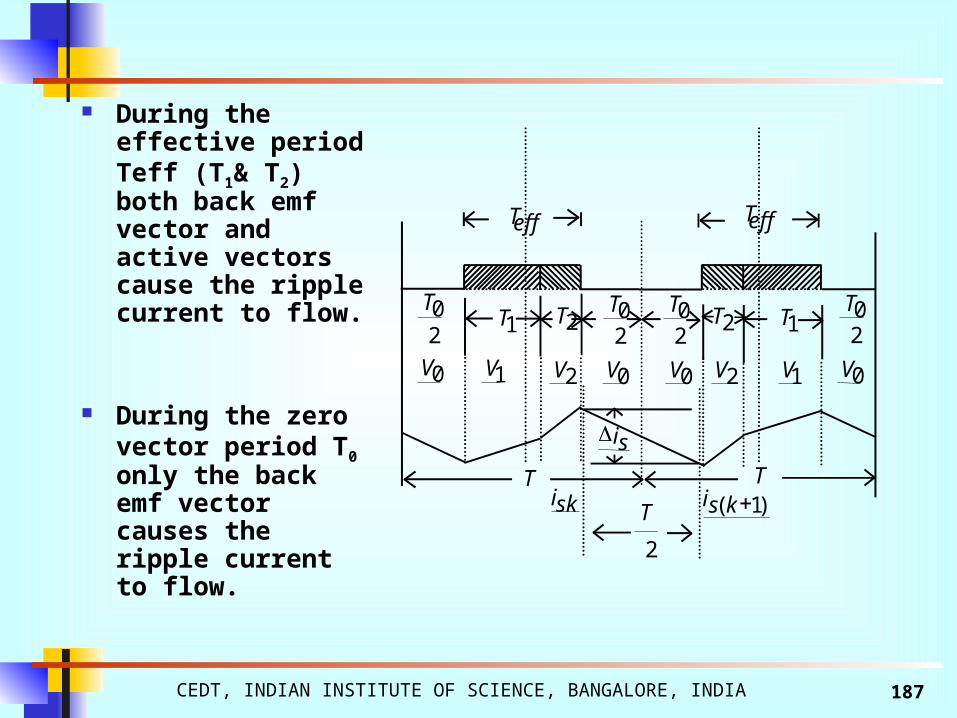
During the effective period Teff (T1& T2) both back emf vector and active vectors cause the ripple current to flow.
During the zero vector period T0
only the back emf vector causes the ripple current to flow.
20T
2T 2T
ski
20T
20T
1T
1V
20T
0V 0V 0V 0V
)1( ksi
effT
2V
1T
1V 2V
2
T
si
T T
effT

CEDT, INDIAN INSTITUTE OF SCIENCE, BANGALORE, INDIA 188
Two samples of current vectors are taken in T/2 time period difference during the zero vector period.
When the modulating frequency is less than 50% of the base frequency the zero vector period T0 is more than the the effective period Teff i.e. T0 is more than half of the switching period T/2 and hence there is sufficient deviation in current vector during zero period T0 .
Flux position estimation in low speed region

CEDT, INDIAN INSTITUTE OF SCIENCE, BANGALORE, INDIA 189
Flux position estimation in high speed region
Three samples of current are taken at t = 0, t = T/2 and t = T. Effective period Teff is more than T/2(half of the
switching period).
Ripple current dependent on the two consecutive active vectors and the back emf vector.
The flux position is estimated by creation of a virtual short circuit i.e. by eliminating the effect of active vectors from the ripple current.

CEDT, INDIAN INSTITUTE OF SCIENCE, BANGALORE, INDIA 190
When the reference vector position θ is within 30˚ from the first active vector in any sector, i.e. 0 < θ <= 30˚, the time period T1 for the first active vector, is greater than the time period T2 for the second active vector
Three samples of current are taken at t = 0, t = T/2 and t = T
20T
20T
effT
1T 2T
0V 1V 2V 0V
1errI 2errI
ski )1( ksi )2( ksi
2
T
2
T

CEDT, INDIAN INSTITUTE OF SCIENCE, BANGALORE, INDIA 191
2
T
2
T
20T
20T
effT
1T 2T
0V 1V 2V 0V
1errI 2errI
ski )1( ksi )2( ksi
When the reference vector position θ is more than 30˚ from the first active vector in a sector i.e. 30˚ < θ <= 60˚,the time period T1 for the first active vector is less than the time period T2 for the second active vector
Three samples of current are taken at t = 0, t = T/2 and t = T
CEDT, INDIAN INSTITUTE OF SCIENCE, BANGALORE, INDIA 192
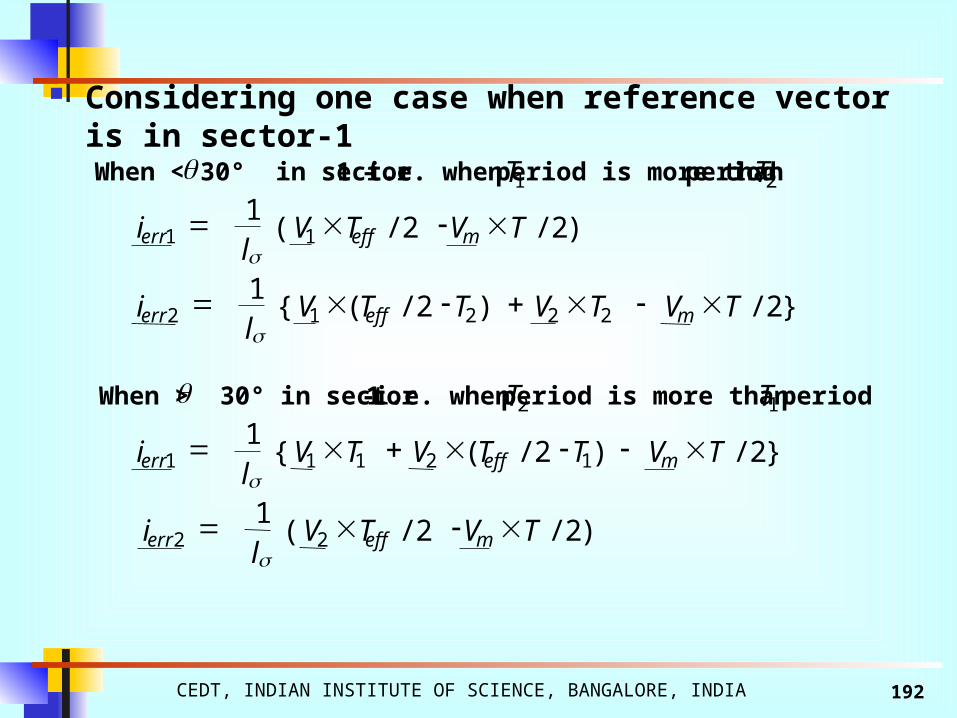
Considering one case when reference vector is in sector-1
When < 30° in sector-1 i.e. when 1T period is more than 2T period
)2/2/(1
11 TVTVl
i mefferr
}2/)2/({1
22212 TVTVTTVl
i mefferr
When > 30° in sector-1 i.e. when 2T period is more than 1T period
}2/)2/({1
12111 TVTTVTVl
i mefferr
)2/2/(1
22 TVTVl
i mefferr
CEDT, INDIAN INSTITUTE OF SCIENCE, BANGALORE, INDIA 193
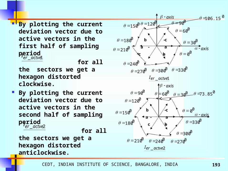
By plotting the current deviation vector due to active vectors in the first half of sampling period
for all the sectors we get a hexagon distorted clockwise.
By plotting the current deviation vector due to active vectors in the second half of sampling period
for all the sectors we get a hexagon distorted anticlockwise.
00
030
0120 090
b -c
-a a
c -b
0150
0180
0210
0240 0270
0300 0330
axis
060
axis
00
030
0120
090
b -c
-a a
c -b
0150
0180
0210 0240
0270
0300
axis
060
1_ actveerI
2_ actveerI
axis
0330
0106.15
073.85
1_ actveeri
2_ actveeri

CEDT, INDIAN INSTITUTE OF SCIENCE, BANGALORE, INDIA 194
By extracting the fundamental components we get that , the fundamental component of lags by Φ from
, the fundamental component of reference vector and , the fundamental component of leads by Φ from
.
Φ = 16.15˚.
fV
1_ actveerfI
2_ actveerfI
t
t
t
1_ actveerfi
1_ actveeri
fV
2_ actveerfi
2_ actveeri
fV
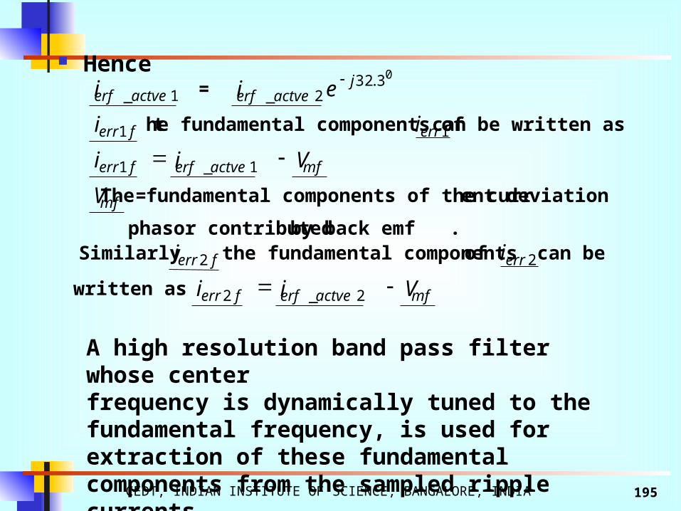
CEDT, INDIAN INSTITUTE OF SCIENCE, BANGALORE, INDIA 195
Hence 1_actveerfi =
03.322_
jactveerf ei
ferri 1 t he fundamental components of 1erri can be written as
mfactveerfferr Vii 1_1
mfV = The fundamental components of the current deviation
phasor contributed by back emf . Similarly ferri 2 the fundamental components of 2erri can be
written as mfactveerfferr Vii 2_2
A high resolution band pass filter whose center frequency is dynamically tuned to the fundamental frequency, is used for extraction of these fundamental components from the sampled ripple currents .

CEDT, INDIAN INSTITUTE OF SCIENCE, BANGALORE, INDIA 196
From the three equations the back emf position is found as
The rotor flux position leads by 90˚ from the back emf position, hence it can be obtained by adding 90˚ to the position of back emf vector.
A speed control scheme is implemented based on the estimated rotor flux position.
)1(0
0
3.32
3.3221
j
jferrferr
mfe
eiiV

CEDT, INDIAN INSTITUTE OF SCIENCE, BANGALORE, INDIA 197
Block diagram of sensorless speed control scheme
V/F actual
slipW
*slipW
*Vsd
*Vsq
Isd
*
*
*
c
b
a
V
V
V
2 – phase to 3 – phase Tra nsfn
I N V E R T E R
***cba VVV
Low Pass Filter
K
Threshold
sW V/F estimator
V/F ref
mfbW
Isq
*Isd
*Isq PI
PI
PI
setW *mrefW
Soft Start
ba ii
ba ii
Current change calculation
Flux Position estimator
est
est
Isd
Isq 3- phase
to dq Slip calculation
sW 3- phase to dq
Slip calculation

CEDT, INDIAN INSTITUTE OF SCIENCE, BANGALORE, INDIA 198
Flux position at frequency equal to 10 hertz.
Flux position at frequency equal to 30 hertz.
Experimental Results
CEDT, INDIAN INSTITUTE OF SCIENCE, BANGALORE, INDIA 199
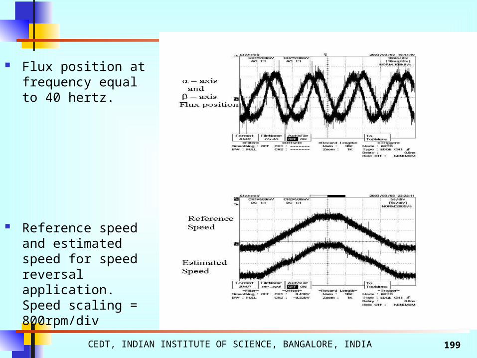
Flux position at frequency equal to 40 hertz.
Reference speed and estimated speed for speed reversal application. Speed scaling = 800rpm/div

CEDT, INDIAN INSTITUTE OF SCIENCE, BANGALORE, INDIA 200
Phase current and estimated speed for speed reversal application. Current scaling = 5A/div, Speed scaling = 800rpm/div.
Speed reversal (zoomed).
CEDT, INDIAN INSTITUTE OF SCIENCE, BANGALORE, INDIA 201
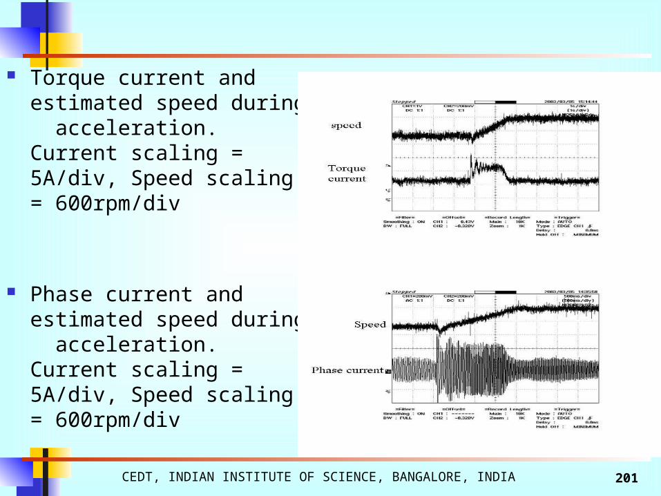
Torque current and estimated speed during acceleration. Current scaling = 5A/div, Speed scaling = 600rpm/div
Phase current and estimated speed during acceleration. Current scaling = 5A/div, Speed scaling = 600rpm/div

CEDT, INDIAN INSTITUTE OF SCIENCE, BANGALORE, INDIA 202
A Five-level Inverter Topology With Common-mode Voltage Elimination for Induction Motor Drives

CEDT, INDIAN INSTITUTE OF SCIENCE, BANGALORE, INDIA 203
• A five-level inverter topology and the switching state selection strategy for the PWM control, is proposed.
• The proposed scheme completely eliminates the common-mode voltages in the entire modulation range of the induction motor drive.
• The proposed scheme is based on a dual five-level inverter fed open-end winding induction motor configuration.
• With the absence of common-mode voltage, associated problems, such as, shaft voltages, bearing currents, etc., are also eliminated in the proposed drive.
Introduction
• A five-level inverter topology is proposed.
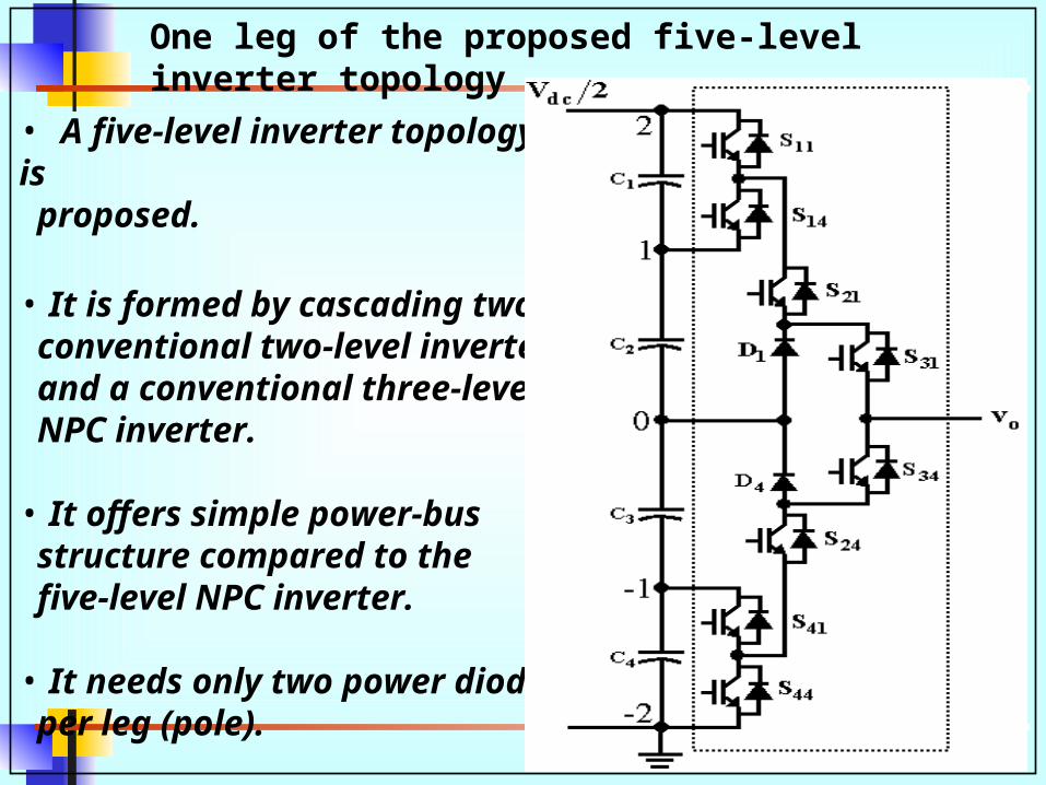
• It is formed by cascading two conventional two-level inverters and a conventional three-level NPC inverter. • It offers simple power-bus structure compared to the five-level NPC inverter. • It needs only two power diodes per leg (pole).
One leg of the proposed five-level inverter topology

CEDT, Indian Institute of Science CEDT, INDIAN INSTITUTE OF SCIENCE, BANGALORE, INDIA 205
*[“1” ON, “0” OFF]**S11-S14, S21-S34, S24-S31, and S41-S44 are
complementary pairs of switches
Realization of the five different voltage levels
Voltage
Level
PoleVolta
ge
State of the switch**
S11 S21 S24 S41
2 Vdc/4 1 1 0 1
1 Vdc/8 0 1 0 1
0 0 0 0 0 1
-1 -Vdc/8 0 0 1 1
-2 -Vdc/4 0 0 1 0
IGBT Gating Logic*

Requirement of blocking voltage capability of devices
• The requirement of blocking voltage capability of individual device goes to as low as
Vdc/8 for S11, S14, S41, and S44 while, it is Vdc/5.33 (3xVdc/2x8) for S21, S34, S24, and S31 in the proposed open-end winding IM drive.

CEDT, INDIAN INSTITUTE OF SCIENCE, BANGALORE, INDIA 207
Power schematic of the dual-five level inverter fed IM drive
CEDT, INDIAN INSTITUTE OF SCIENCE, BANGALORE, INDIA 208
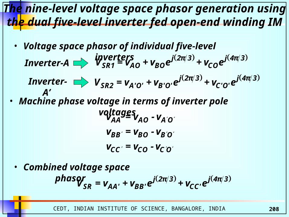
The nine-level voltage space phasor generation using the dual five-level inverter fed open-end winding IM
• Voltage space phasor of individual five-level inverters
• Machine phase voltage in terms of inverter pole voltages
j 2π 3 j 4π 3SR1 AO BO COV = v + v e + v e
j 2π 3 j 4π 3SR2 A'O' B'O' C'O'V = v + v e + v e
AA AO A O
BB BO B O
CC CO C O
v = v - v
v = v - v
v = v - v
j 2π 3 j 4π 3SR AA' BB' CC'V = v + v e + v e
Inverter-A
Inverter-A’
• Combined voltage space phasor
CEDT, INDIAN INSTITUTE OF SCIENCE, BANGALORE, INDIA 209
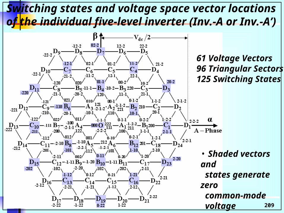
Switching states and voltage space vector locations of the individual five-level inverter (Inv.-A or Inv.-A’)
61 Voltage Vectors96 Triangular Sectors125 Switching States
• Shaded vectors and states generate zero common-mode voltage