Embed Size (px)
Citation preview

Electronic Materials Letters, Vol. 9, No. 3 (2013), pp. 371-374
CdS Nanopowder and Nanofilm: Simultaneous Synthesis and
Structural Analysis
Suresh Kumar, Pankaj Sharma,* and Vineet Sharma
Department of Physics and Materials Science, Jaypee University of Information Technology, Waknaghat, H.P. (173234) India
(received date: 5 September 2012 / accepted date: 7 January 2013 / published date: 10 May 2013)
Chemical bath deposition technique has been used for simultaneous synthesis of CdS nanopowder andnanofilm. X-ray diffraction (XRD), Scanning Electron Microscopy (SEM) and Atomic Force Microscopy(AFM) studies show a predominant α-CdS structure. Structural parameters show a random lattice disorderand bond length contraction leading to high density of nanopowder and nanofilm in comparison to standardCdS. The columnar structure growth of the nanofilm devoid of grain boundaries may be explored forwindow layers.
Keywords: nanocrystalline materials, optical materials, lattice defects, atomic force microscopy (AFM), X-raydiffraction (XRD)
1. INTRODUCTION
Because of the unique shape, size and tunable physio-chemical properties in low dimensional nanostructuredmaterials, these are used for various scientific and technologicalapplications.[1] Major efforts have been devoted to synthesizebinary metal chalcogenide of group II-VI semiconductors innanocrystalline form owing to the quantum confinement andtheir potential applications.[2-6] Due to wide band gap,compact unit cell and electron affinity, CdS is preferred forcoating over other p-type semiconducting materials as anoptical window layer.[7-9] CdS exists in two crystalline formsviz. cubic - zinc blende (β-CdS) and hexagonal- wurtzite (α-CdS) phases.[10,11] Both these phases are closely related andshare several common inter-planar spacing.[12,13] The freeenergies of formation of both forms differ marginally andcoexistence of a mixed phase has often been observed.[10,13,14]
Present work reports on the synthesis and structuralanalysis of nanopowder (NP) and nanofilm (NF) of CdS. It isan effort to understand physical and structural characteristics ofnanosized CdS particulates, in powder and film form,obtained under similar growth conditions. Besides, to thebest of our knowledge such work has rarely been reportedparticularly for CdS. XRD, SEM and AFM have been usedfor micro structural and morphological analysis of CdSpowder and film in nano range.
2. EXPERIMENTAL PROCEDURE
For simultaneous synthesis of CdS nanopowder andnanofilm, ammonia solution (2 M) was added drop wiseinto the aqueous solution of cadmium chloride (0.02 M), tilltransparent solution was obtained. The complexing agent(ammonia) was able to dissolve the white precipitates ofCd(OH)2 under constant stirring and form cadmium-tetra-amine complex (Cd(NH3)4
2+). A clean glass substrate wasinclined vertically in the solution for film deposition. Finally,aqueous solution of thiourea (0.04 M) was added. Constantstirring at 300 rpm, temperature 343 K ± 2 K and pH 11 ±0.1 was maintained during the reaction process for a growthperiod of 45 min. The formation of CdS from the reactantsolution had an initial stage of nucleation. In this stageCd(OH)2 was formed in the solution and on substrate as aninitial layer. This Cd(OH)2 was chemically converted intoCd(NH3)4
2+ complex reacting with NH4OH. Finally, Cd(NH3)42+
reacted with S2− ions available in the bath from hydrolysis ofthiourea. Hence, CdS in the form of layer on the substrateand as powder in solution was obtained. The former wasgrowth mechanism on the substrate surface via ion by ionprocess and latter, the agglomeration of colloids in solutionvia cluster by cluster process.[10,13] The obtained powder andfilm were thermally annealed in air at 573 K ± 5 K for 1 h.CdS nanofilm and nanopowder were characterized forsurface morphology and microstructure by using XRD(PANalytical's X’Pert-PRO), SEM (ZEISS EVO40) andAFM (NTMDT-NTEGRA).
*Corresponding author: [email protected] ©KIM and Springer
DOI: 10.1007/s13391-013-2151-1
372 S. Kumar et al.
Electron. Mater. Lett. Vol. 9, No. 3 (2013)
3. RESULTS AND DISCUSSION
The intensity of prominent reflection plane (002) shown inFig. 1 has been observed to be high for NF as compared toNP. The diffused back ground in XRD pattern of NP (Fig.1(a)) indicates the formation of weak crystalline structure.This behavior may be due to distorted periodicity of latticeelements and short range order structure of nano crystallites.However, NF has smooth XRD pattern (Fig. 1(b)). This maybe attributed to the high crystallinity and long range order oflarge crystallites. Both samples have multiple reflectionpeaks with broad profile reflecting polycrystalline nature andexistence of nano crystallites. Besides, samples exhibitprominent α-CdS phase. NP (Fig. 1(a)) has additional peaksat 2θ = 29.82°, 31.84° and 55.14° that correspond to (200)reflections of β-CdS, (002) reflection of hcp - Cd and (004)/(222) reflection of mixed α and β-CdS phases respectively.[15,16]
However, for NF (Fig. 1(b)), only one additional peak at2θ = 24.03° corresponding to (222) phase of orthorhombic[16]
(α-S8) has been observed. Thus, NF has prominent α-CdS
structure with rich crystalline state in comparison to NP. Thegrowth of NP via cluster by cluster process may be attributedto predominant β-CdS phase in comparison to α-CdSstructure. In NF, ion-by-ion growth process may be responsiblefor enhancing α-CdS structure.
The occurrence of hcp phase of Cd in NP and orthorhombicα-S8 in NF may be attributed to the size of Cd2+ and S2− ions.In the later stages of reaction, the large size Cd2+ ions aremore favored in solution whereas, in the initial stage thetendency for adsorption of small S2− ions on substrate ismore in comparison to Cd2+ ions. The identical nature of 2θand (hkl) suggests that the growth of CdS in solution and itsadsorption on the substrate have evolved under the samegrowth parameters. The dhkl values are in reasonable agreementwith standard dhkl values of CdS.[15]
The texture coefficient (TChkl)[17] is a measure of the degree
of orientation of each reflection in contrast to a randomlyoriented sample. TChkl indicates that NF has higher degree oforientation (TChkl = 3.54 at 2θ = 26.68°) in comparison to NP(TChkl = 1.27 at 2θ = 26.75°). For NF, crystallites illustratestrong orientation along (002) plane whereas, for NP theyare weakly oriented. The evolution of the texture duringgrowth mechanism has a strong effect on surface features ofgrains. The initial ion-by-ion growth on substrate contributesto the strong texture development in comparison to cluster-by-cluster growth in the residue.
SEM micrograph of NP (Fig. 2(a)) consists of nanocrystallites and their aggregates. The formation of compactagglomerates and flocks of crystallites in NP may be due tohomogeneous precipitation of CdS. The nano crystallites areembedded densely in these clusters. SEM micrograph of NF(Fig. 2(b)) shows the surface of film to be homogeneous anduniformly spread, devoid of pores and cracks. The averagesize of individually accessible crystallites in NP micrographis 5 nm - 20 nm whereas, for NF, it is 10 nm - 100 nm.
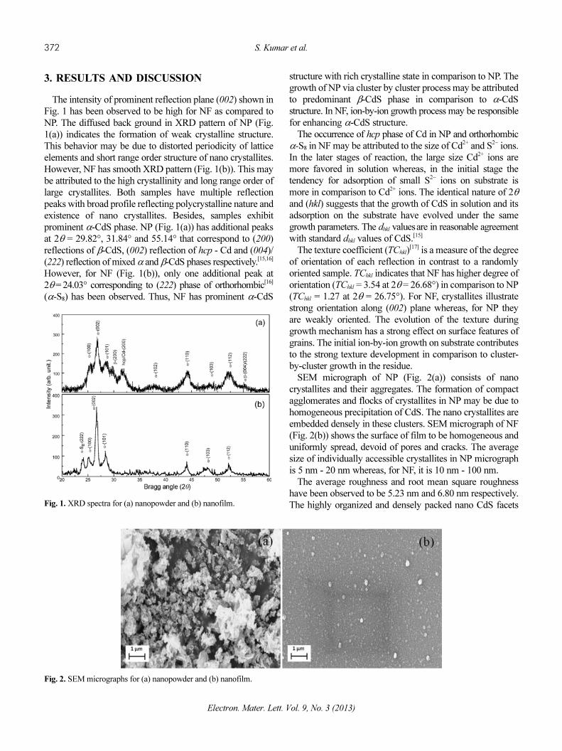
The average roughness and root mean square roughnesshave been observed to be 5.23 nm and 6.80 nm respectively.The highly organized and densely packed nano CdS facetsFig. 1. XRD spectra for (a) nanopowder and (b) nanofilm.
Fig. 2. SEM micrographs for (a) nanopowder and (b) nanofilm.
S. Kumar et al. 373
Electron. Mater. Lett. Vol. 9, No. 3 (2013)
have been observed for NF (Fig. 3(a)). CdS particles grow incolumnar structure parallel to the plane of substrate (Fig.3(b)) indicating the growth of hexagonal-wurtzite structurewith (002) orientation. Hence, no grain boundaries arepresent in NF to disrupt the flow of charge carriers. Thisaspect may be explored for application of NF in windowlayers.
The lattice constants a and c for hexagonal structure havebeen determined by analytical method.[18] The average latticeconstants for NP are, a = 4.083 Å and c = 6.659 Å withcorresponding c/a ratio = 1.6311 Å whereas, for NF they are,a = 4.093 Å and c = 6.677 Å with c/a ratio = 1.6314 Årespectively. The error in the calculation of a and c is± 2.4 × 10⁻³ Å and ± 3.5 × 10⁻³ Å respectively. The c/a ratiofor both the samples has been found to be slightly greaterthan the standard value (1.623) for the α-CdS.[15] Thus, forNP and NF, the lattice deviation along c-axis is high. In NP,both the lattice constants are less than standard value,[15]
which indicates that crystallites in NP are under compressivestrain. However, higher c value for NF indicates tensilestrain.[18] The lattice constants of the nanoparticles aredifferent from the bulk particles due to the existence ofdefects like surface or interface stress, strain, grain boundaries,dislocations, etc. The deviations in c/a ratios are 0.80% and0.84% for NP and NF respectively and is <1% confirming amarginal structural distortion.
In a real crystal, the wurtzite structure deviates from theideal arrangement due to changing c/a axial ratio andinternal parameter (uip)
[19] (for NP and NF, uip = 0.375). Theparameter uip represents the shift of anionic sub-lattice tocationic sub-lattice in z-direction. The structural deviationdue to the change in c/a ratio is responsible for contraction orexpansion of lattice and hence, bond length (LCd-S)
[19] (for NPand NF, LCd-S = 2.499 Å and 2.506 Å respectively). Thelattice deviation in terms of distortion parameter (εv),
[19] forNP and NF is −0.0338 and −0.0264 respectively. The unitcell volume (for NP = 96.133 Å3 and and NF = 96.873 Å3),
uip and LCd-S are less than the standard value[15] for both NPand NF. At the same time negative value of εv and higherdensity (for NP and NF = 4.992 g/cc and 4.954 g/ccrespectively) w.r.t. standard CdS[15] directly indicate thatthere is a contraction of the lattice. In nano crystallinematerials, the smaller surface energy of the nanocrystallitescause size contraction and solidification by elastic distortionof lattice.[20] The correlated arrangement in nanoparticles isalso responsible for the random lattice disorder and bondlength contraction. This contracted bond length stiffens thenanoparticles leading to high density.[21]
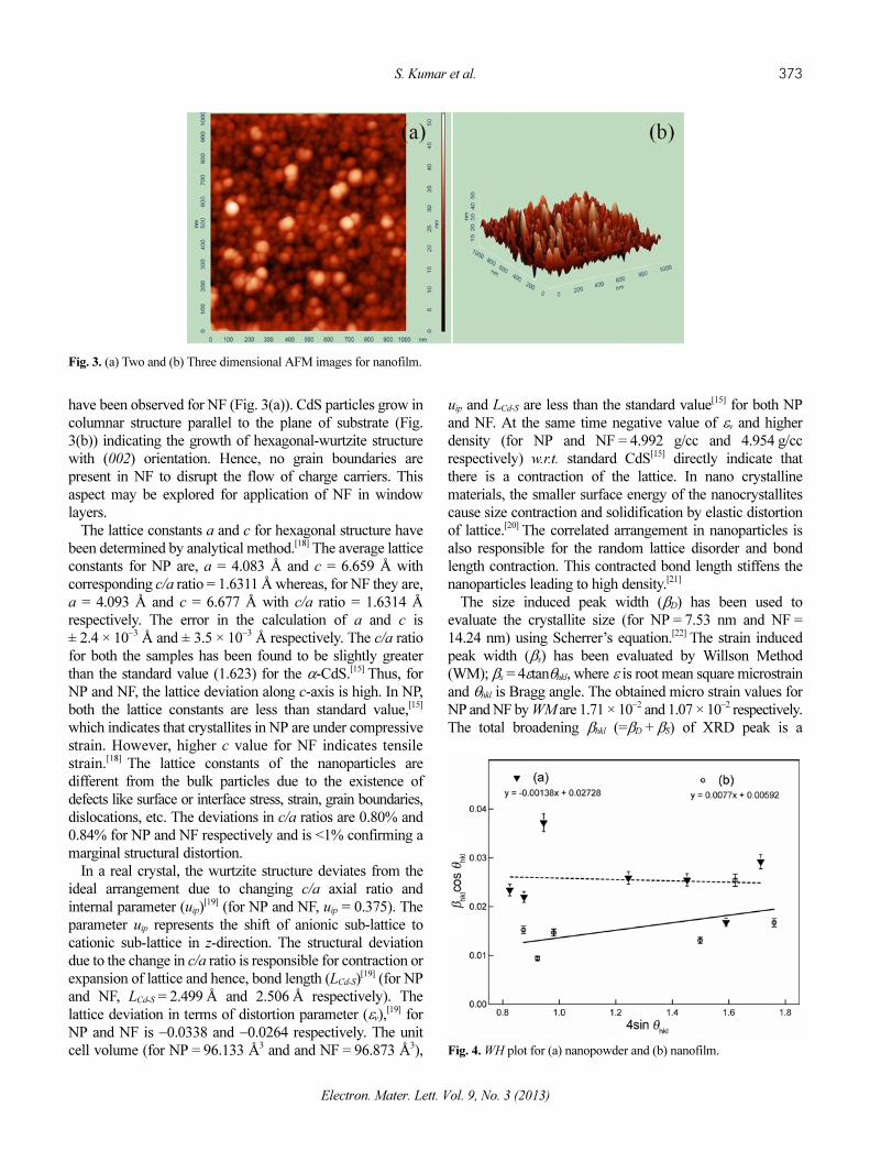
The size induced peak width (βD) has been used toevaluate the crystallite size (for NP = 7.53 nm and NF =14.24 nm) using Scherrer’s equation.[22] The strain inducedpeak width (βs) has been evaluated by Willson Method(WM); βs = 4εtanθhkl, where ε is root mean square microstrainand θhkl is Bragg angle. The obtained micro strain values forNP and NF by WM are 1.71 × 10⁻² and 1.07 × 10⁻² respectively.The total broadening βhkl (=βD + βS) of XRD peak is a
Fig. 3. (a) Two and (b) Three dimensional AFM images for nanofilm.
Fig. 4. WH plot for (a) nanopowder and (b) nanofilm.
374 S. Kumar et al.
Electron. Mater. Lett. Vol. 9, No. 3 (2013)
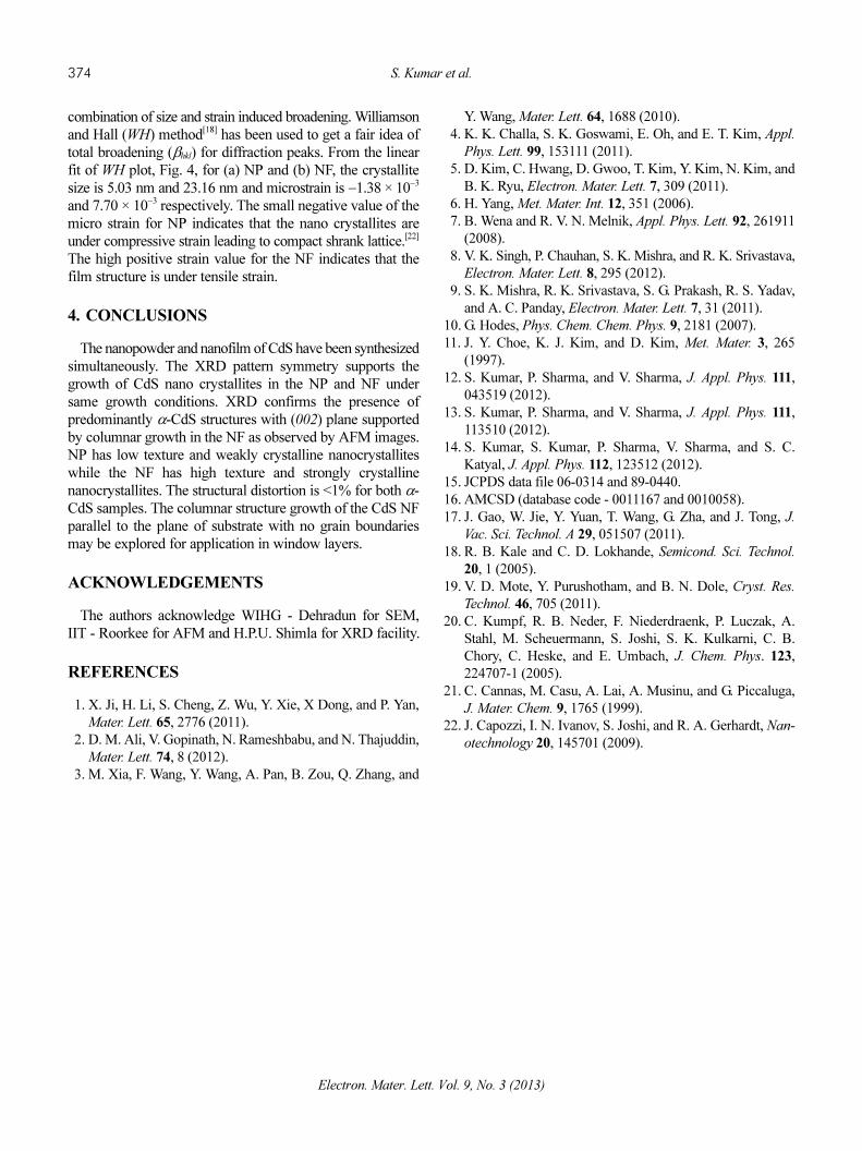
combination of size and strain induced broadening. Williamsonand Hall (WH) method[18] has been used to get a fair idea oftotal broadening (βhkl) for diffraction peaks. From the linearfit of WH plot, Fig. 4, for (a) NP and (b) NF, the crystallitesize is 5.03 nm and 23.16 nm and microstrain is −1.38 × 10⁻³
and 7.70 × 10⁻³ respectively. The small negative value of themicro strain for NP indicates that the nano crystallites areunder compressive strain leading to compact shrank lattice.[22]
The high positive strain value for the NF indicates that thefilm structure is under tensile strain.
4. CONCLUSIONS
The nanopowder and nanofilm of CdS have been synthesizedsimultaneously. The XRD pattern symmetry supports thegrowth of CdS nano crystallites in the NP and NF undersame growth conditions. XRD confirms the presence ofpredominantly α-CdS structures with (002) plane supportedby columnar growth in the NF as observed by AFM images.NP has low texture and weakly crystalline nanocrystalliteswhile the NF has high texture and strongly crystallinenanocrystallites. The structural distortion is <1% for both α-CdS samples. The columnar structure growth of the CdS NFparallel to the plane of substrate with no grain boundariesmay be explored for application in window layers.
ACKNOWLEDGEMENTS
The authors acknowledge WIHG - Dehradun for SEM,IIT - Roorkee for AFM and H.P.U. Shimla for XRD facility.
REFERENCES
1. X. Ji, H. Li, S. Cheng, Z. Wu, Y. Xie, X Dong, and P. Yan,
Mater. Lett. 65, 2776 (2011).
2. D. M. Ali, V. Gopinath, N. Rameshbabu, and N. Thajuddin,
Mater. Lett. 74, 8 (2012).
3. M. Xia, F. Wang, Y. Wang, A. Pan, B. Zou, Q. Zhang, and
Y. Wang, Mater. Lett. 64, 1688 (2010).
4. K. K. Challa, S. K. Goswami, E. Oh, and E. T. Kim, Appl.
Phys. Lett. 99, 153111 (2011).
5. D. Kim, C. Hwang, D. Gwoo, T. Kim, Y. Kim, N. Kim, and
B. K. Ryu, Electron. Mater. Lett. 7, 309 (2011).
6. H. Yang, Met. Mater. Int. 12, 351 (2006).
7. B. Wena and R. V. N. Melnik, Appl. Phys. Lett. 92, 261911
(2008).
8. V. K. Singh, P. Chauhan, S. K. Mishra, and R. K. Srivastava,
Electron. Mater. Lett. 8, 295 (2012).
9. S. K. Mishra, R. K. Srivastava, S. G. Prakash, R. S. Yadav,
and A. C. Panday, Electron. Mater. Lett. 7, 31 (2011).
10. G. Hodes, Phys. Chem. Chem. Phys. 9, 2181 (2007).
11. J. Y. Choe, K. J. Kim, and D. Kim, Met. Mater. 3, 265
(1997).
12. S. Kumar, P. Sharma, and V. Sharma, J. Appl. Phys. 111,
043519 (2012).
13. S. Kumar, P. Sharma, and V. Sharma, J. Appl. Phys. 111,
113510 (2012).
14. S. Kumar, S. Kumar, P. Sharma, V. Sharma, and S. C.
Katyal, J. Appl. Phys. 112, 123512 (2012).
15. JCPDS data file 06-0314 and 89-0440.
16. AMCSD (database code - 0011167 and 0010058).
17. J. Gao, W. Jie, Y. Yuan, T. Wang, G. Zha, and J. Tong, J.
Vac. Sci. Technol. A 29, 051507 (2011).
18. R. B. Kale and C. D. Lokhande, Semicond. Sci. Technol.
20, 1 (2005).
19. V. D. Mote, Y. Purushotham, and B. N. Dole, Cryst. Res.
Technol. 46, 705 (2011).
20. C. Kumpf, R. B. Neder, F. Niederdraenk, P. Luczak, A.
Stahl, M. Scheuermann, S. Joshi, S. K. Kulkarni, C. B.
Chory, C. Heske, and E. Umbach, J. Chem. Phys. 123,
224707-1 (2005).
21. C. Cannas, M. Casu, A. Lai, A. Musinu, and G. Piccaluga,
J. Mater. Chem. 9, 1765 (1999).
22. J. Capozzi, I. N. Ivanov, S. Joshi, and R. A. Gerhardt, Nan-
otechnology 20, 145701 (2009).