Embed Size (px)
Citation preview
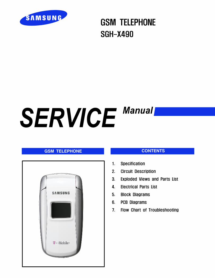
GSM TELEPHONE
SGH-X490
GSM TELEPHONE CONTENTS
1. Specification
2. Circuit Description
3. Exploded Views and Parts List
4. Electrical Parts List
5. Block Diagrams
6. PCB Diagrams
7. Flow Chart of Troubleshooting
Samsung Electronics Co.,Ltd. December. 2005
Printed in Korea.
Code No.: GH68-08926A
BASIC.
This Service Manual is a property of Samsung Electronics Co.,Ltd.Any unauthorized use of Manual can be punished under applicableInternational and/or domestic law.
ⓒ

SAMSUNG Proprietary-Contents may change without notice
1. Specification
This Document can not be used without Samsung's authorization
1-1
GSM900Phase 1
EGSM900Phase 2
DCS1800Phase 1
PC1900Phase 1
Freq. Band[MHz]Upl ink/Downlink
890~915935~960
880~915925~960
1710~17851805~1880
1850~19101930~1990
ARFCN range 1~124 0~124 &915~1023 512~885 512~810
Tx/Rx spacing 45MHz 45MHz 95MHz 80MHz
Mod. Bit rate/Bi t Per iod
270.833kbps3.692us
270.833kbps3.692us
270.833kbps3.692us
270.833kbps3.692us
Time SlotPeriod/Frame Period
576.9us4.615ms
576.9us4.615ms
576.9us4.615ms
576.9us4.615ms
Modulat ion 0.3GMSK 0.3GMSK 0.3GMSK 0.3GMSK
MS Power 33dBm~5dBm 33dBm~5dBm 30dBm~0dBm 30dBm~0dBm
Power Class 5pcl ~ 19pcl 5pcl ~ 19pcl 0pcl ~ 15pcl 0pcl ~ 15pcl
Sensi t ivi ty -102dBm -102dBm -100dBm -100dBm
TDMA Mux 8 8 8 8
Cell Radius 35Km 35Km 2Km 2Km
1-1. GSM General Specification

SAMSUNG Proprietary-Contents may change without noticeThis Document can not be used without Samsung's authorization
Specification
1-2
TX Powercontrol level
GSM900
5 33±3 dBm
6 31±3 dBm
7 29±3 dBm
8 27±3 dBm
9 25±3 dBm
10 23±3 dBm
11 21±3 dBm
12 19±3 dBm
13 17±3 dBm
14 15±3 dBm
15 13±3 dBm
16 11±5 dBm
17 9±5dBm
18 7±5 dBm
19 5±5 dBm
TX Powercontrol level
DCS1800
0 30±3 dBm
1 28±3 dBm
2 26±3 dBm
3 24±3 dBm
4 22±3 dBm
5 20±3 dBm
6 18±3 dBm
7 16±3 dBm
8 14±3 dBm
9 12±4 dBm
10 10±4 dBm
11 8±4dBm
12 6±4 dBm
13 4±4 dBm
14 2±5 dBm
15 0±5 dBm
1-2. GSM TX power class
TX Powercontrol level
PCS1900
0 30±3 dBm
1 28±3 dBm
2 26±3 dBm
3 24±3 dBm
4 22±3 dBm
5 20±3 dBm
6 18±3 dBm
7 16±3 dBm
8 14±3 dBm
9 12±4 dBm
10 10±4 dBm
11 8±4dBm
12 6±4 dBm
13 4±4 dBm
14 2±5 dBm
15 0±5 dBm
SAMSUNG Proprietary-Contents may change without notice
2. Circuit Description
2-1
This Document can not be used without Samsung's authorization
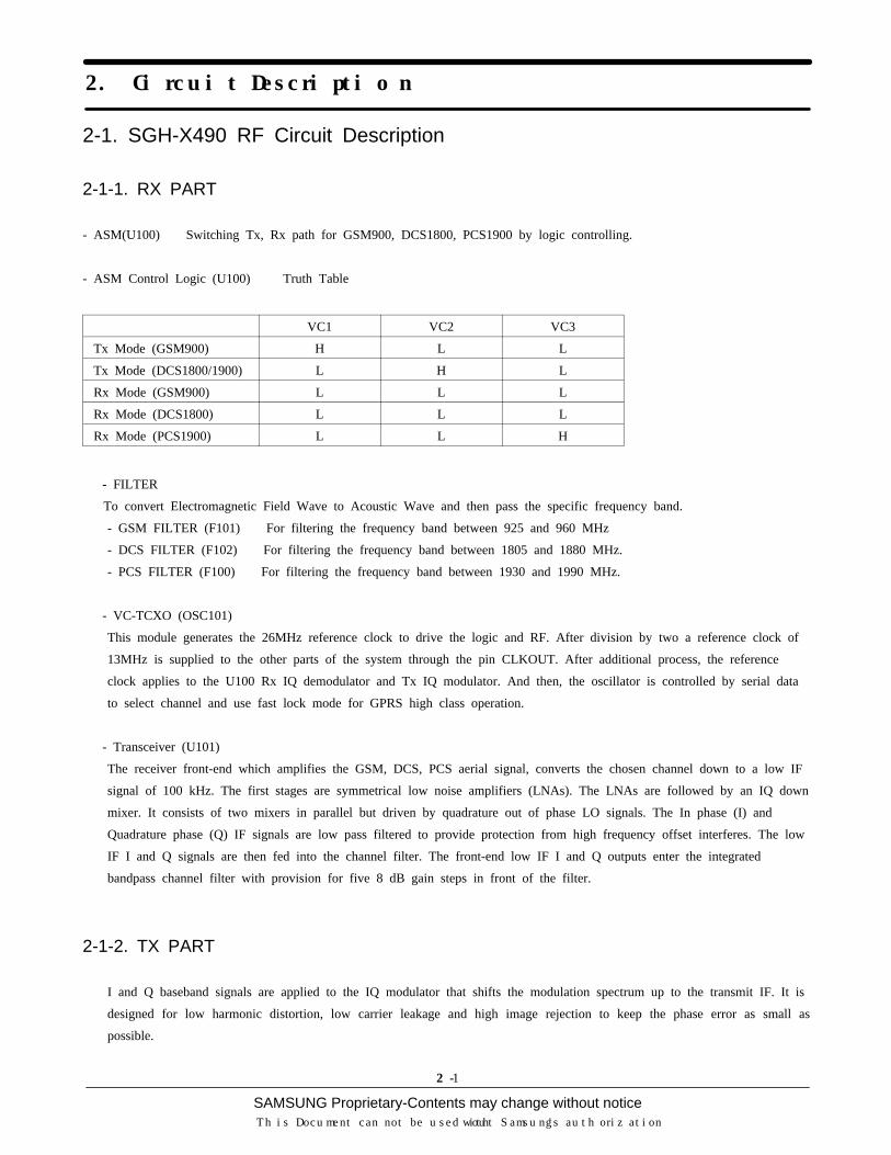
2-1. SGH-X490 RF Circuit Description
2-1-1. RX PART
- ASM(U100) → Switching Tx, Rx path for GSM900, DCS1800, PCS1900 by logic controlling.
- ASM Control Logic (U100) → Truth Table
VC1 VC2 VC3
Tx Mode (GSM900) H L L
Tx Mode (DCS1800/1900) L H L
Rx Mode (GSM900) L L L
Rx Mode (DCS1800) L L L
Rx Mode (PCS1900) L L H
- FILTER
To convert Electromagnetic Field Wave to Acoustic Wave and then pass the specific frequency band.
- GSM FILTER (F101) → For filtering the frequency band between 925 and 960 MHz
- DCS FILTER (F102) → For filtering the frequency band between 1805 and 1880 MHz.
- PCS FILTER (F100) → For filtering the frequency band between 1930 and 1990 MHz.
- VC-TCXO (OSC101)
This module generates the 26MHz reference clock to drive the logic and RF. After division by two a reference clock of
13MHz is supplied to the other parts of the system through the pin CLKOUT. After additional process, the reference
clock applies to the U100 Rx IQ demodulator and Tx IQ modulator. And then, the oscillator is controlled by serial data
to select channel and use fast lock mode for GPRS high class operation.
- Transceiver (U101)
The receiver front-end which amplifies the GSM, DCS, PCS aerial signal, converts the chosen channel down to a low IF
signal of 100 kHz. The first stages are symmetrical low noise amplifiers (LNAs). The LNAs are followed by an IQ down
mixer. It consists of two mixers in parallel but driven by quadrature out of phase LO signals. The In phase (I) and
Quadrature phase (Q) IF signals are low pass filtered to provide protection from high frequency offset interferes. The low
IF I and Q signals are then fed into the channel filter. The front-end low IF I and Q outputs enter the integrated
bandpass channel filter with provision for five 8 dB gain steps in front of the filter.
2-1-2. TX PART
I and Q baseband signals are applied to the IQ modulator that shifts the modulation spectrum up to the transmit IF. It is
designed for low harmonic distortion, low carrier leakage and high image rejection to keep the phase error as small as
possible.
SAMSUNG Proprietary-Contents may change without notice
Circuit Description
2-2
This Document can not be used without Samsung's authorization
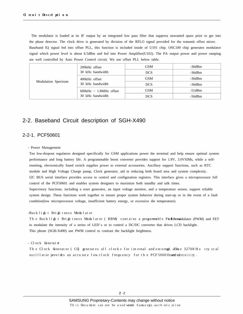
The modulator is loaded at its IF output by an integrated low pass filter that suppress unwanted spurs prior to get into
the phase detector. The clock drive is generated by division of the RFLO signal provided for the transmit offset mixer.
Baseband IQ signal fed into offset PLL, this function is included inside of U101 chip. OSC100 chip generates modulator
signal which power level is about 6.5dBm and fed into Power Amplifier(U102). The PA output power and power ramping
are well controlled by Auto Power Control circuit. We use offset PLL below table.
Modulation Spectrum
200kHz offset30 kHz bandwidth
GSM -36dBm
DCS -36dBm
400kHz offset30 kHz bandwidth
GSM -36dBm
DCS -36dBm
600kHz ~ 1.8MHz offset30 kHz bandwidth
GSM -51dBm
DCS -56dBm
2-2. Baseband Circuit description of SGH-X490
2-2-1. PCF50601
- Power Management
Ten low-dropout regulators designed specifically for GSM applications power the terminal and help ensure optimal system
performance and long battery life. A programmable boost converter provides support for 1.8V, 3.0VSIMs, while a self-
resetting, electronically fused switch supplies power to external accessories. Ancillary support functions, such as RTC
module and High Voltage Charge pump, Clock generator, aid in reducing both board area and system complexity.
I2C BUS serial interface provides access to control and configuration registers. This interface gives a microprocessor full
control of the PCF50601 and enables system designers to maximize both standby and talk times.
Supervisory functions. including a reset generator, an input voltage monitor, and a temperature sensor, support reliable
system design. These functions work together to ensure proper system behavior during start-up or in the event of a fault
condition(low microprocessor voltage, insufficient battery energy, or excessive die temperature).
-Backlight Brightness Modulator
The Backlight Brightness Modulator (BBM) contains a programmable Pulse-width modulator (PWM) and FET
to modulate the intensity of a series of LED’ s or to control a DC/DC converter that drives LCD backlight.
This phone (SGH-X490) use PWM control to contrast the backlight brightness.
- Clock Generator
The Clock Generator (CG) generates all clocks for internal and external usage. The 32768 Hz crystal
oscillator provides an accurate low clock frequency for the PCF50601 and other circuitry.

SAMSUNG Proprietary-Contents may change without notice
Circuit Description
2-3
This Document can not be used without Samsung's authorization
2-2-2. LCD ConnectorLCD is consisted of main LCD(color 65K UFB LCD) and sub LCD (B/W LCD).
Chip select signals LCD_MAIN_CS and LCD_SUB_CS, can enable Each LCD. BACKLIGHT signal enables white LED
of main LCD. "LCD_RESET" signal initiates the reset process of the LCD.
16-bit data lines(HD(0)~HD(15)) transfers data and commands to LCD. Data and commands use "HA(1)" signal. If this
signal is low, inputs to LCD are commands. If it is high, inputs to LCD are data.
The signal which informs the state of LCD is whether input or output, is required. But in this system, there is no input
state from LCD. So only "HA(1)" signal is used to indicate write data or command to LCD. Power signals for LCD are
"VBAT and "VDD3".
"SPK_P" and "SPK_N" are used for audio speaker containing voice or melody. And "VDD_VIB" from PCF50601
enables the motor.
2-2-3. KeyThis is consisted of key interface pins among OM6359, KBIO(0:7). These signals compose the matrix. Result of matrix
informs the key status to key interface in the OM6359. Power on/off key is separated from the matrix. So power on/off
signal is connected with PCF50601 to enable PCF50601. Twelve key LEDs are use the "VDD_KEY" as supply voltage.
"FLIP" informs the status of folder (open or closed) to the OM6359. This uses the hall effect IC, A321ELH-SAMSUNG.
A magnet under main LCD enables A321ELH-SAMSUNG.
2-2-4. EMI ESD FilterThis system uses the EMI ESD filter, EMIF09 to protect noise from IF CONNECTOR part.
2-2-5. IF connetorIt is 18-pin connector. They are designed to use VBAT, V_EXT_CHARGE, TXD0, RXD0, RTS0, CTS0, JIG_REC,
CHARGER_OK, RXD1, TXD1, AUX_MIC, AUX_SPK and GND. They connected to power supply IC, microprocessor
and signal processor IC.
2-2-6. Battery Charge ManagementA complete constant-current/constant-voltage linear charger is used for single cell lithium-ion batteries.
If TA connected to phone, "+DCVOLT" enable charger IC and supply current to battery.
When fault condition caused, "CHG_ON" signal level change low to high and charger IC stop charging
process.
2-2-7. AudioEARP_P and EARP_N from OM6359 are connected to the main speaker. MIC_P and MIC_N are connected to the main
MIC. YMU788 is a synthesizer LSI for mobile phones. It is a LSI as an input/output device for sound sources, which is
the mobile phones, such as MP3, AAC, etc, in addition to ringing-melodies.
As a synthesis, YMU788 is equipped 32 voices with different tones. Since the device is capable of simultaneously
generating up to synchronous with the play of the FM synthesizer, various sampled voices can be used as sound effects.
Since the play data of YMU788 are interpreted at anytime through FIFO, the length of the data(playing period) is not
limited, so the device can flexibly support application such as incoming call melody music distribution service.
SAMSUNG Proprietary-Contents may change without notice
Circuit Description
2-4
This Document can not be used without Samsung's authorization
The hardware sequencer built in this device allows playing of the complex music without giving excessive load to the
CPU of the portable telephones.
For the purpose of enabling YMU788 to demonstrate its full capabilities, Yamaha purpose to use "SMAF:Synthetic music
Mobile Application Format" as a data distribution format that is compatible with multimedia. Since the SMAF takes a
structure that sets importance on the synchronization between sound and images, various contents can be written into it
including incoming call melody with words that can be used for training karaoke, and commercial channel that combines
texts, images and sounds, and others. The hardware sequencer of YMU788 directly interprets and plays blocks relevant to
synthesis (playing music and reproducing ADPCM with FM synthesizer) that are included in data distributed in SMAF.
2-2-8. MemorySignals in the OM6359 enable two memories. They use two volt supply voltage, VDD3 in the PCF50601 & VDD_1.9V
with a LDO. This system uses Intel's memory, RD38F3050LOZTQ0. It is consisted of 128M bits flash NOR memory and
64M bits SRAM. It has 16 bit data line, HD[0~15] which is connected to OM6359. It has 26 bit address lines,
HA[1~26]. NCSFLASH & NCSRAM signals are chip select. Writing process, HWR_N is low and it enables writing
process to flash memory and SRAM. During reading process, HRD_N is low and it enables reading process to flash
memory and SRAM. Reading or writing procedure is processed after HWR_N or HRD_N is enabled.
2-2-9. OM6359OM6359 is consisted of ARM core and DSP core. It has 8x1Kword on-chip program/data RAM, 55 Kwords
on-chip program ROM in the DSP. It has 4K*32bits ROM and 2K*32bits RAM in the ARM core. DSP is consisted
of KBS, JTAG, EMI and UART. ARM core is consisted of EMI, PIC(Programmable Interrupt Controller),
reset/power/clock unit, DMA controller, TIC(Test Interface Controller), peripheral bridge, PPI, SSI(Synchronous Serial
Interface), ACC(Asynchronous communications controllers), timer, ADC, RTC(Real-Time Clock) and keyboard interface.
KBIO(0:7), address lines of DSP core and HD[0~15]. HA[1~26], address lines of ARM core and HD[0~15], data lines of
ARM core are connected to memory, YMU788.
NCSRAM, NCSFLASH in the ARM core are connected to each memory. HWR_N and HRD_N control the process of
memory. External IRQ(Interrupt ReQuest) signals from each units, such as, PMU need the compatible process.
KBIO[0~7] receive the status from key and RXD0/TXD0 are used for the communication using data link
cable(DEBUG_DTR/RTS/TXD/RXD/CTS/DSR).
It has JTAG control pins(TDI/TDO/TCK) for ARM core and DSP core. It receives 13MHz clock in CKI pin from
external TCXO. ADC(Analog to Digital Convertor) part receives the status of temperature, battery type and battery voltage.
2-2-10. TOH2600DGI4KRA(26MHz)This system uses the 26MHz TCXO, TOH2600DGI4KRA, SEM. AFC control signal from OM6359 controls frequency
from 26MHz x-tal. The clock output frequency of UAA3536 is 13MHz. This clock is connected to OM6359, YMU788.
SAMSUNG Proprietary-Contents may change without notice
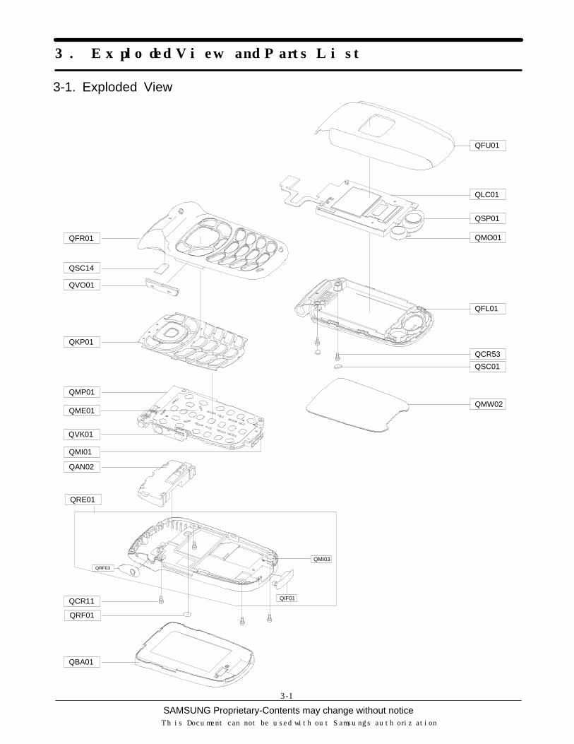
3. Exploded View and Parts List
3-1
This Document can not be used without Samsung's authorization
3-1. Exploded View
QIF01
QMI03
QFR01
QSC14
QMP01
QKP01
QVO01
QME01
QAN02
QRE01
QCR11
QRF03
QMI01
QBA01
QFU01
QSP01
QMO01
QLC01
QFL01
QMW02
QSC01QCR53
QRF01
QVK01

SAMSUNG Proprietary-Contents may change without notice
Exploded view and Part List
3-2
This Document can not be used without Samsung's authorization
Location NO. Description SEC CODE
QAN02 INTENNA-SGHX490 GH42-00699A
QBA01 BATTERY-1000MAH,WH/SIL,MAIN GH43-02197A
QCR11 SCREW-MACHINE 6001-001654
QCR53 SCREW-MACHINE 6001-001639
QFL01 MEC-FOLDER LOWER GH75-08664A
QFR01 MEC-FRONT COVER GH75-06966A
QFU01 MEC-FOLDER UPPER GH75-06471A
QKP01 MEC-KEYPAD(TMB/WST) GH75-08152A
QLC01 MEA-LCD MODULE KIT(X495) GH97-05095A
QME01 UNIT-METAL DOME GH59-02046A
QMI01 MICROPHONE-ASSY-SGHX497 GH30-00198A
QMO01 MOTOR DC-SGHZ130 GH31-00154D
QMP01 PBA MAIN-SGHX490 GH92-02444A
QMW02 PCT-WINDOW MAIN GH72-19918B
QRF01 MPR-RF SHEET GH74-14435B
QSC01 MPR-SCREW SHEET GH74-13610B
QSC14 MPR-TAPE FRONT FPC GH74-08876A
QSP01 SPEAKER 3001-001779
QVK01 UNIT-VOLUME KEY GH59-02053A
QVO01 MEC-VOLUME KEY GH75-07274A
QRE01 MEC-REAR COVER GH75-08454A
QRF03 PMO-EAR COVER GH72-23535A
QIF01 PMO-IF COVER GH72-23556A
QMI03 RMO-RUBBER MIC REAR GH73-04847A
3-2. Parts List

SAMSUNG Proprietary-Contents may change without notice
Exploded view and Part List
3-3
This Document can not be used without Samsung's authorization
Description SEC CODE
CARD-REGISTRATION 6801-001446
BAG PE 6902-000634
CBF INTERFACE-SGHS500 TEST CAB GH39-00217A
CBF SIGNAL-SGHE800TEST GH39-00283A
ADAPTOR-TAD GH44-00482A
LABEL(P)-WATER SOAK GH68-02026A
MANUAL-USER GH68-08536A
LABEL(R)-MAIN(EU) GH68-08622A
CUSHION-CASE(1-2) GH69-03333A
BOX(P)-UNIT(T-MOBILE) GH69-03459A
PMO-BATT LOCKER GH72-19954A
PCT-WINDOW SUB GH72-19964A
RMO-RUBBER TOP LCD A GH73-04923A
RMO-RUBBER TOP LCD B GH73-04924A
MPR-BOHO VINYL SUB(S-R) GH74-03429B
MPR-BOHO VINYL REAR GH74-12905A
MPR-TAPE WINDOW SUB GH74-13223A
MPR-TAPE WINDOW MAIN GH74-13608A
MPR-BOHO VINYL SUB GH74-14432A
MPR-TAPE EL GH74-14881A
MPR-BOHO VINYL LCD CONN GH74-15350A
MPR-TAPE PBA EMI GH74-15484A
MPR-SPONGE MOTOR GH74-15610A
MPR-SPONGE PBA GH74-15911A
MPR-TAPE PBA A GH74-16066A
MPR-BOHO VINYL MAIN GH74-16545B
MPR-BOHO VINYL MAIN(S) GH74-16545C
MPR-BOHO VINYL SUB GH74-17302A
INSTALL-SGHS500 TEST JIG GH80-01909A

SAMSUNG Proprietary-Contents may change without notice
Exploded view and Part List
3-4
This Document can not be used without Samsung's authorization
3-3. Test Jig (GH80-01909A)
3-3-1. RF Test Cable(GH39-00283A)
3-3-2. Test Cable(GH39-00217A)
3-3-3. Serial Cable
3-3-4. Power Supply Cable 3-3-5. DATA CABLE(GH39-00219A)
3-3-6. TA(GH44-00184G)

SAMSUNG Proprietary-Contents may change without notice
4. Electrical Parts List
4-1
This Document can not be used without Samsung's authorization
Design LOC Description SEC CODE STATUS
BAT300 BATTERY-LI(2ND) 4302-001180 SAC101 C-CER,CHIP 2203-000278 SAC102 C-CER,CHIP 2203-000812 SAC103 C-CER,CHIP 2203-000854 SAC104 C-CER,CHIP 2203-000854 SAC105 C-CER,CHIP 2203-000278 SAC106 C-CER,CHIP 2203-000278 SAC107 C-CER,CHIP 2203-000854 SAC108 C-CER,CHIP 2203-005057 SAC109 C-CER,CHIP 2203-005482 SAC110 C-CER,CHIP 2203-005057 SAC111 C-CER,CHIP 2203-005482 SAC112 C-CER,CHIP 2203-000233 SAC113 C-CER,CHIP 2203-000233 SAC114 C-CER,CHIP 2203-005482 SAC115 C-CER,CHIP 2203-005057 SAC116 C-CER,CHIP 2203-005138 SAC117 C-CER,CHIP 2203-001383 SAC118 C-CER,CHIP 2203-000359 SAC119 C-CER,CHIP 2203-000696 SAC120 C-CER,CHIP 2203-000836 SAC121 C-CER,CHIP 2203-001101 SAC122 C-CER,CHIP 2203-005482 SAC123 C-CER,CHIP 2203-005057 SAC124 C-CER,CHIP 2203-006053 SAC125 C-CER,CHIP 2203-000438 SAC126 C-CER,CHIP 2203-000233 SAC127 C-TA,CHIP 2404-001239 SAC128 C-CER,CHIP 2203-006141 SAC129 C-CER,CHIP 2203-000438 SAC130 C-CER,CHIP 2203-006190 SAC132 C-CER,CHIP 2203-005503 SAC133 C-CER,CHIP 2203-000311 SAC134 C-CER,CHIP 2203-000233 SAC135 C-CER,CHIP 2203-000254 SAC136 C-CER,CHIP 2203-001153 SAC137 C-CER,CHIP 2203-000550 SAC138 C-CER,CHIP 2203-006137 SAC139 C-CER,CHIP 2203-005482 SAC140 C-CER,CHIP 2203-000679 SAC141 C-CER,CHIP 2203-005482 SAC142 C-CER,CHIP 2203-005057 SAC143 C-CER,CHIP 2203-000233 SAC144 C-CER,CHIP 2203-000254 SAC145 C-CER,CHIP 2203-000438 SAC146 C-CER,CHIP 2203-000438 SAC147 C-CER,CHIP 2203-000438 SAC152 C-CER,CHIP 2203-000278 SAC153 C-CER,CHIP 2203-000278 SAC156 C-CER,CHIP 2203-000438 SA

SAMSUNG Proprietary-Contents may change without notice
Electrical Parts List
4-2
This Document can not be used without Samsung's authorization
Design LOC Description SEC CODE STATUS
C157 C-CER,CHIP 2203-000359 SAC158 C-CER,CHIP 2203-000359 SAC200 C-CER,CHIP 2203-005061 SAC203 C-CER,CHIP 2203-005061 SAC204 C-CER,CHIP 2203-000254 SAC206 C-CER,CHIP 2203-005061 SAC207 C-CER,CHIP 2203-000254 SAC208 C-CER,CHIP 2203-000254 SAC210 C-CER,CHIP 2203-006423 SAC212 C-CER,CHIP 2203-005061 SAC213 C-CER,CHIP 2203-005482 SAC214 C-CER,CHIP 2203-000854 SAC215 C-CER,CHIP 2203-006423 SAC216 C-CER,CHIP 2203-000854 SAC218 C-CER,CHIP 2203-005061 SAC219 C-CER,CHIP 2203-005482 SAC220 C-CER,CHIP 2203-000254 SAC221 C-CER,CHIP 2203-006423 SAC222 C-CER,CHIP 2203-006423 SAC223 C-CER,CHIP 2203-005482 SAC224 C-CER,CHIP 2203-000438 SAC225 C-CER,CHIP 2203-005482 SAC300 C-CER,CHIP 2203-005482 SAC301 C-CER,CHIP 2203-006105 SAC302 C-CER,CHIP 2203-005482 SAC304 C-TA,CHIP 2404-001394 SAC305 C-CER,CHIP 2203-005482 SAC306 C-CER,CHIP 2203-005482 SAC307 C-TA,CHIP 2404-001374 SAC308 C-CER,CHIP 2203-006257 SAC309 C-CER,CHIP 2203-005482 SAC310 C-CER,CHIP 2203-006208 SAC311 C-TA,CHIP 2404-001225 SAC312 C-CER,CHIP 2203-005395 SAC313 C-CER,CHIP 2203-000386 SAC314 C-CER,CHIP 2203-005482 SAC315 C-CER,CHIP 2203-006257 SAC316 C-CER,CHIP 2203-000386 SAC317 C-CER,CHIP 2203-006562 SAC318 C-CER,CHIP 2203-000386 SAC319 C-CER,CHIP 2203-006562 SAC320 C-CER,CHIP 2203-006053 SAC321 C-CER,CHIP 2203-000885 SAC322 C-CER,CHIP 2203-006208 SAC323 C-CER,CHIP 2203-006324 SAC324 C-CER,CHIP 2203-000812 SAC325 C-CER,CHIP 2203-005065 SAC326 C-TA,CHIP 2404-001225 SAC327 C-TA,CHIP 2404-001225 SAC328 C-CER,CHIP 2203-005482 SA

SAMSUNG Proprietary-Contents may change without notice
Electrical Parts List
4-3
This Document can not be used without Samsung's authorization
Design LOC Description SEC CODE STATUS
C329 C-CER,CHIP 2203-005482 SAC330 C-CER,CHIP 2203-005482 SAC332 C-CER,CHIP 2203-006257 SAC333 C-CER,CHIP 2203-006562 SAC334 C-CER,CHIP 2203-006208 SAC335 C-CER,CHIP 2203-006208 SAC336 C-CER,CHIP 2203-000679 SAC337 C-CER,CHIP 2203-006053 SAC338 C-CER,CHIP 2203-006208 SAC339 C-CER,CHIP 2203-006208 SAC340 C-CER,CHIP 2203-006053 SAC400 C-TA,CHIP 2404-001348 SAC401 C-CER,CHIP 2203-000995 SAC402 C-CER,CHIP 2203-005482 SAC403 C-CER,CHIP 2203-005061 SAC404 C-CER,CHIP 2203-006562 SAC406 C-CER,CHIP 2203-000278 SAC407 C-CER,CHIP 2203-000679 SAC408 C-CER,CHIP 2203-005482 SAC409 C-CER,CHIP 2203-005061 SAC410 C-CER,CHIP 2203-005736 SAC411 C-CER,CHIP 2203-000679 SAC412 C-CER,CHIP 2203-005482 SAC413 C-CER,CHIP 2203-000679 SAC415 C-CER,CHIP 2203-000489 SAC416 C-CER,CHIP 2203-000679 SAC418 C-CER,CHIP 2203-000278 SAC419 C-CER,CHIP 2203-006423 SAC420 C-CER,CHIP 2203-005736 SAC421 C-CER,CHIP 2203-000885 SAC422 C-CER,CHIP 2203-000254 SAC423 C-CER,CHIP 2203-001153 SAC424 C-CER,CHIP 2203-005483 SAC425 C-CER,CHIP 2203-005483 SAC426 C-CER,CHIP 2203-006562 SAC429 C-CER,CHIP 2203-000995 SAC430 C-CER,CHIP 2203-000995 SAC437 C-CER,CHIP 2203-006053 SAC438 C-CER,CHIP 2203-005482 SAC439 C-TA,CHIP 2404-001352 SAC501 C-CER,CHIP 2203-002443 SAC502 C-CER,CHIP 2203-005482 SAC503 C-CER,CHIP 2203-005482 SAC504 C-CER,CHIP 2203-000278 SAC505 C-CER,CHIP 2203-000679 SAC507 C-CER,CHIP 2203-000995 SAC508 C-CER,CHIP 2203-000278 SAC509 C-CER,CHIP 2203-000995 SAC510 C-CER,CHIP 2203-000995 SAC511 C-CER,CHIP 2203-000278 SA

SAMSUNG Proprietary-Contents may change without notice
Electrical Parts List
4-4
This Document can not be used without Samsung's authorization
Design LOC Description SEC CODE STATUS
C513 C-CER,CHIP 2203-006562 SAC514 C-CER,CHIP 2203-006562 SAC515 C-CER,CHIP 2203-006562 SA
CN300 CONNECTOR-CARD EDGE 3709-001355 SACN502 CONNECTOR-INTERFACE 3710-001611 SACN503 HEADER-BATTERY 3711-005783 SA
CON101 CONNECTOR-COAXIAL 3705-001358 SAEAR400 JACK-EAR PHONE 3722-002067 SA
F100 FILTER-SAW 2904-001571 SAF101 FILTER-SAW 2904-001550 SAF102 FILTER-SAW 2904-001570 SAHEA1 HEADER-BOARD TO BOARD 3711-005728 SAL101 INDUCTOR-SMD 2703-002207 SAL102 INDUCTOR-SMD 2703-002199 SAL103 INDUCTOR-SMD 2703-002207 SAL104 INDUCTOR-SMD 2703-002203 SAL105 INDUCTOR-SMD 2703-002700 SAL106 INDUCTOR-SMD 2703-001726 SAL107 INDUCTOR-SMD 2703-002308 SAL108 INDUCTOR-SMD 2703-002700 SAL109 INDUCTOR-SMD 2703-002308 SAL110 INDUCTOR-SMD 2703-002308 SAL111 INDUCTOR-SMD 2703-002199 SAL112 INDUCTOR-SMD 2703-002176 SAL113 INDUCTOR-SMD 2703-001727 SAL114 INDUCTOR-SMD 2703-002176 SAL115 INDUCTOR-SMD 2703-002203 SAL116 INDUCTOR-SMD 2703-002368 SAL117 INDUCTOR-SMD 2703-001708 SAL300 BEAD-SMD 3301-001105 SAL400 BEAD-SMD 3301-001362 SAL401 BEAD-SMD 3301-001362 SAL402 BEAD-SMD 3301-001105 SAL403 BEAD-SMD 3301-001105 SAL501 BEAD-SMD 3301-001438 SA
LED501 LED 0601-002037 SALED502 LED 0601-002037 SALED503 LED 0601-002037 SALED504 LED 0601-002037 SALED505 LED 0601-002037 SALED506 LED 0601-002037 SALED507 LED 0601-002037 SALED508 LED 0601-002037 SALED509 LED 0601-002037 SALED510 LED 0601-002037 SALED511 LED 0601-002037 SALED512 LED 0601-002037 SAOSC100 OSCILLATOR-VCO 2806-001326 SAOSC101 OSCILLATOR-VCTCXO 2809-001281 SA
Q100 TR-DIGITAL 0504-001151 SA

SAMSUNG Proprietary-Contents may change without notice
Electrical Parts List
4-5
This Document can not be used without Samsung's authorization
Design LOC Description SEC CODE STATUS
R101 R-CHIP 2007-000162 SAR102 R-CHIP 2007-000162 SAR103 R-CHIP 2007-000162 SAR104 R-CHIP 2007-007148 SAR105 R-CHIP 2007-000141 SAR106 R-CHIP 2007-007528 SAR107 R-CHIP 2007-001288 SAR108 R-CHIP 2007-000171 SAR109 R-CHIP 2007-001329 SAR110 R-CHIP 2007-000144 SAR111 R-CHIP 2007-001308 SAR112 R-CHIP 2007-001308 SAR113 R-CHIP 2007-000566 SAR114 R-CHIP 2007-000148 SAR115 R-CHIP 2007-001288 SAR116 R-CHIP 2007-007311 SAR117 R-CHIP 2007-000566 SAR118 R-CHIP 2007-007699 SAR119 R-CHIP 2007-007699 SAR120 R-CHIP 2007-001308 SAR121 R-CHIP 2007-001308 SAR122 R-CHIP 2007-000171 SAR123 R-CHIP 2007-000171 SAR125 R-CHIP 2007-008672 SAR126 R-CHIP 2007-001308 SAR127 R-CHIP 2007-000142 SAR128 R-CHIP 2007-000148 SAR129 R-CHIP 2007-000138 SAR130 R-CHIP 2007-008213 SAR131 R-CHIP 2007-008213 SAR132 R-CHIP 2007-008213 SAR133 R-CHIP 2007-008213 SAR134 R-CHIP 2007-000140 SAR135 R-CHIP 2007-000140 SAR136 R-CHIP 2007-000171 SAR200 R-CHIP 2007-000174 SAR201 R-CHIP 2007-008055 SAR204 R-CHIP 2007-000162 SAR205 R-CHIP 2007-008055 SAR206 R-CHIP 2007-008055 SAR207 R-CHIP 2007-008055 SAR208 R-CHIP 2007-008052 SAR209 R-CHIP 2007-008516 SAR210 R-CHIP 2007-008055 SAR211 R-CHIP 2007-007107 SAR212 R-CHIP 2007-007142 SAR213 R-CHIP 2007-007001 SAR214 R-CHIP 2007-007142 SAR215 R-CHIP 2007-001284 SAR216 R-CHIP 2007-000148 SA

SAMSUNG Proprietary-Contents may change without notice
Electrical Parts List
4-6
This Document can not be used without Samsung's authorization
Design LOC Description SEC CODE STATUS
R217 R-CHIP 2007-001284 SAR218 R-CHIP 2007-000162 SAR219 R-CHIP 2007-000162 SAR220 R-CHIP 2007-007107 SAR221 R-CHIP 2007-007001 SAR222 R-CHIP 2007-000171 SAR223 R-CHIP 2007-008588 SAR224 R-CHIP 2007-008588 SAR225 R-CHIP 2007-008542 SAR227 R-CHIP 2007-008542 SAR228 R-CHIP 2007-008542 SAR300 R-CHIP 2007-000157 SAR301 R-CHIP 2007-000148 SAR302 R-CHIP 2007-007573 SAR303 R-CHIP 2007-007334 SAR304 R-CHIP 2007-008117 SAR305 R-CHIP 2007-000151 SAR306 R-CHIP 2007-007100 SAR400 R-CHIP 2007-002796 SAR401 R-CHIP 2007-000140 SAR402 R-CHIP 2007-000148 SAR403 R-CHIP 2007-008054 SAR404 R-CHIP 2007-000140 SAR405 R-CHIP 2007-008542 SAR406 R-CHIP 2007-008055 SAR407 R-CHIP 2007-002796 SAR408 R-CHIP 2007-008055 SAR409 R-CHIP 2007-007334 SAR410 R-CHIP 2007-001313 SAR411 R-CHIP 2007-008542 SAR412 R-CHIP 2007-007483 SAR413 R-CHIP 2007-007589 SAR414 R-CHIP 2007-007138 SAR415 R-CHIP 2007-007981 SAR416 R-CHIP 2007-007488 SAR417 R-CHIP 2007-007489 SAR418 R-CHIP 2007-000138 SAR422 R-CHIP 2007-000138 SAR424 R-CHIP 2007-008542 SAR500 R-CHIP 2007-000162 SAR501 R-CHIP 2007-008055 SAR502 R-CHIP 2007-008531 SAR503 R-CHIP 2007-008531 SAR504 R-CHIP 2007-008531 SAR505 R-CHIP 2007-008531 SAR506 R-CHIP 2007-008531 SAR507 R-CHIP 2007-000162 SAR508 R-CHIP 2007-008531 SAR510 R-CHIP 2007-001298 SAR511 R-CHIP 2007-001298 SA

SAMSUNG Proprietary-Contents may change without notice
Electrical Parts List
4-7
This Document can not be used without Samsung's authorization
Design LOC Description SEC CODE STATUS
R512 R-CHIP 2007-001298 SAR513 R-CHIP 2007-001298 SAR514 R-CHIP 2007-001298 SAR515 R-CHIP 2007-001298 SAR516 R-CHIP 2007-001298 SAR517 R-CHIP 2007-001298 SAR518 R-CHIP 2007-001298 SAR519 R-CHIP 2007-001298 SAR520 R-CHIP 2007-001298 SAR521 R-CHIP 2007-001298 SAR522 R-CHIP 2007-008055 SAR529 R-CHIP 2007-008055 SAR530 R-CHIP 2007-008055 SAR531 R-CHIP 2007-009084 SAR532 R-CHIP 2007-009084 SAR533 R-CHIP 2007-009084 SAR534 R-CHIP 2007-009084 SAR535 R-CHIP 2007-009084 SAR536 R-CHIP 2007-009084 SAR537 R-CHIP 2007-009084 SAR538 R-CHIP 2007-009084 SAR539 R-CHIP 2007-009084 SAR540 R-CHIP 2007-009084 SAR541 R-CHIP 2007-009084 SAR542 R-CHIP 2007-009084 SAR543 R-CHIP 2007-009084 SAR544 R-CHIP 2007-009084 SAR545 R-CHIP 2007-009084 SAR546 R-CHIP 2007-009084 SAR547 R-CHIP 2007-000162 SA
SW500 IC-HALL EFFECT S/W 1009-001010 SATH200 THERMISTOR-NTC 1404-001221 SATH501 VARISTOR 1405-001093 SATH502 VARISTOR 1405-001093 SATH503 VARISTOR 1405-001093 SAU100 DUPLEXER-ASM 2909-001246 SAU101 IC-TRANSCEIVER 1205-002327 SAU102 IC-POWER AMP 1201-002075 SAU201 IC-MCP 1108-000019 SAU202 IC-COMM. CONTROLLER 1205-002607 SAU300 IC-BATTERY 1203-003109 SAU301 DIODE-TVS 0406-001200 SAU302 IC-CONTROLLER 1205-002350 SAU303 IC-POSI.FIXED REG. 1203-003808 SAU401 IC-VOLTAGE COMP. 1202-001036 SAU402 IC-ANALOG MULTIPLEX 1001-001306 SAU404 TR-DIGITAL 0504-001100 SAU406 IC-MELODY 1204-002461 SAU408 IC-CMOS LOGIC 0801-002237 SAU501 FILTER-EMI/ESD 2901-001325 SA

SAMSUNG Proprietary-Contents may change without notice
Electrical Parts List
4-8
This Document can not be used without Samsung's authorization
Design LOC Description SEC CODE STATUS
U502 IC-CMOS LOGIC 0801-002882 SAU503 FILTER-EMI/ESD 2901-001246 SAU504 FILTER-EMI/ESD 2901-001325 SAU506 FILTER-EMI/ESD 2901-001325 SAU507 FILTER-EMI/ESD 2901-001325 SAU508 IC-CMOS LOGIC 0801-002882 SAU510 IC-BUS SWITCH 1205-002779 SAU511 IC-BUS SWITCH 1205-002779 SAU512 IC-BUS SWITCH 1205-002779 SAV401 DIODE-TVS 0406-001201 SAV402 DIODE-TVS 0406-001201 SAV501 VARISTOR 1405-001121 SAV502 VARISTOR 1405-001121 SAV504 VARISTOR 1405-001121 SAV505 VARISTOR 1405-001121 SAV506 VARISTOR 1405-001121 SAV507 VARISTOR 1405-001121 SAV509 VARISTOR 1405-001121 SAX300 CRYSTAL-SMD 2801-004339 SA
ZD300 DIODE-ZENER 0403-001427 SAZD401 DIODE-TVS 0406-001201 SAZD402 DIODE-TVS 0406-001197 SAZD406 DIODE-TVS 0406-001201 SAZD501 DIODE-ZENER 0403-001387 SAZD502 DIODE-TVS 0406-001167 SAZD503 DIODE-TVS 0406-001197 SAZD504 DIODE-TVS 0406-001197 SA

SAMSUNG Proprietary-Contents may change without noticeThis Document can not be used without Samsung's authorization
5. Block Diagrams
5-1
5-1. RF Solution Block Diagram
100 kHz+fmod
REFINVC-TCXO
GSM
DCS/PCS
I+
fmodI-
Q+
Q-
~~
VAPC
EPCOS GSM RX SAW Filter B7845 (2.0X1.4)
IL=1.4dB typ 1.5dB maxRipple=0.5dB typ 0.6dB max
Vcc_RF_VCO
Discrete 3rd Order Loop Filter
fc = ? kHz
삼성전기 TX VCOVOT1810F27KRA (6.0X5.0X1.7)
GSM = 880 ~ 915MHz(Vt=0.5V ~ 3.0V )Tuning Sensitivity = 55±11MHz/VDCS = 1710 ~ 1785MHz(Vt=0.5V ~ 3.0V )Tuning Sensitivity = 115±23 MHz/VPout= 6.5±3 dBm typ.,Ic <= 30mA Harmonics <= -10dBc
Micro Devices Quadband PAMRF3146 (7 X 7)
GSM: Pout = 34.2 dBm , E = 55%DCS: Pout= 32.0 dBm , E = 55%
RXON
Vcc_Tx_BURST
VBAT
HITACHI METAL ANT S/W
ESHS-C090TImax = 8 mAFreq (MHz) Loss(typ.)
880 - 915 1.2 dB 925 - 960 0.8 dB 1710 -1910 1.5 dB 1805 -1880 1.2dB
Atten 2xfo : 43dB,26dB(GSM,DCS/PCS)
3xfo : 40dB,26dB(GSM,DCS/PCS)
EN
CLK
DATA
DCS/PCS S/W
OFFSET Mixer input power-16dBm max, -22dBm min
f compRF =26MHz
Philips TransceiverUAA3536
Pins IA,IB,QA and QBV I
Q : 1.25V ty
p. , 1.15V mi
n, 1.35Vmax
V mod : 0.5V pp
QUAD
DIV
PFDCP
VREG
~
Vcc_RF_LO
FracNDIV
1:1/2
VREG
26MHz
Vcc_REF(2.4V typ.)
Vcc_SYN
FE_SW1
FE_SW2
3WBUSCTLREG
PWREN
GSM/DCS/PCS
DIVQUAD
PFDCP
f TXIF
60MHz
+ I OUT-
-+
FESWONSYNONTXON
GSM S/W
PMU
HVS
VDD1 (1.35V min 2.95V max , 150mA )
VBat (3.6V typ 3.0V min)
V_MODE
RF1_VDD
RF2_VDD
RF1_VDDS
RF2_VDDS
VDD2 (1.35V min 3.45V max , 150mA )VDD3 (1.35V min 3.45V max , 100mA )
VDD4 (1.35V min 3.45V max , 150mA )
AVDD(1.35V min 2.65V max , 100mA )
VCC_RX_TX (2.7V ,100mA )VCC_SYN (2.7V , 100mA )
VCC_RF_VCO (2.7V , 100mA )
VCC_CP (4.0V , 25mA )
VCC_TX_BURST (2.7V , 100mA )
PON_SYNT
PON_TX
IL=1.5dB typ 2.1dB maxRipple=0.5dB typ 1.0dB max
I OUT
Q OUTQ OUT
GSM_TX_MODE_SW
VCC_RX_TX
DCS/PCS_TX_MODE_SWInverter circuits
PCS_RX_MODE_SW
Vc_GSM Vc_DCS Vc_PCS(2.7V)
Ripple=0.5dB typ 1.0dB maxIL=1.4dB typ 2.1dB max
EPCOS DCS RX SAW Filter B7852 (2.0X1.4)
EPCOS PCS RX SAW Filter B7851 (2.0X1.4)
1930 -1990 1.2dB
PCS: Pout= 32.0 dBm , E = 52%
(2.7V)
SEM

SAMSUNG Proprietary-Contents may change without notice
Block Diagrams
This Document can not be used without Samsung's authorization
5-2
5-2. Base Band Solution Block Diagram
BatteryType
BatteryVoltage
BatteryTemperature
AFC
RAMP
Charging Circuit
Li-Ion Battery(Standard)
OM6359VIBRATOR
SYSTEM CLOCK(13MHz)
RTC_CLOCK(32.768KHz)
KEY_BOARD
RECEIVER
MIC
LCD
RF INTERFACEVCC_RX_TX
VCC_RF_VCO
VCC_TX_BURST
PMU
VCC_SYN
Serial DataInterface
I/OInterface
A/DInterface
BB INTERFACE
MELODY IC(40 Poly)
SPEAKER
VDD1
VDD2
VDD3
VDD_VIB
MIC_BIAS
VCC_CP
VDD_KEY
VDD_AMP
AVDD
AVDD_TEMP
SIM CARD
BL_VDD

SAMSUNG Proprietary-Contents may change without notice
6. PCB Diagrams
6-1
This Document can not be used without Samsung's authorization
6-1. PCB Top Diagram
SAMSUNG Proprietary-Contents may change without notice
PCB Diagrams
6-2
This Document can not be used without Samsung's authorization
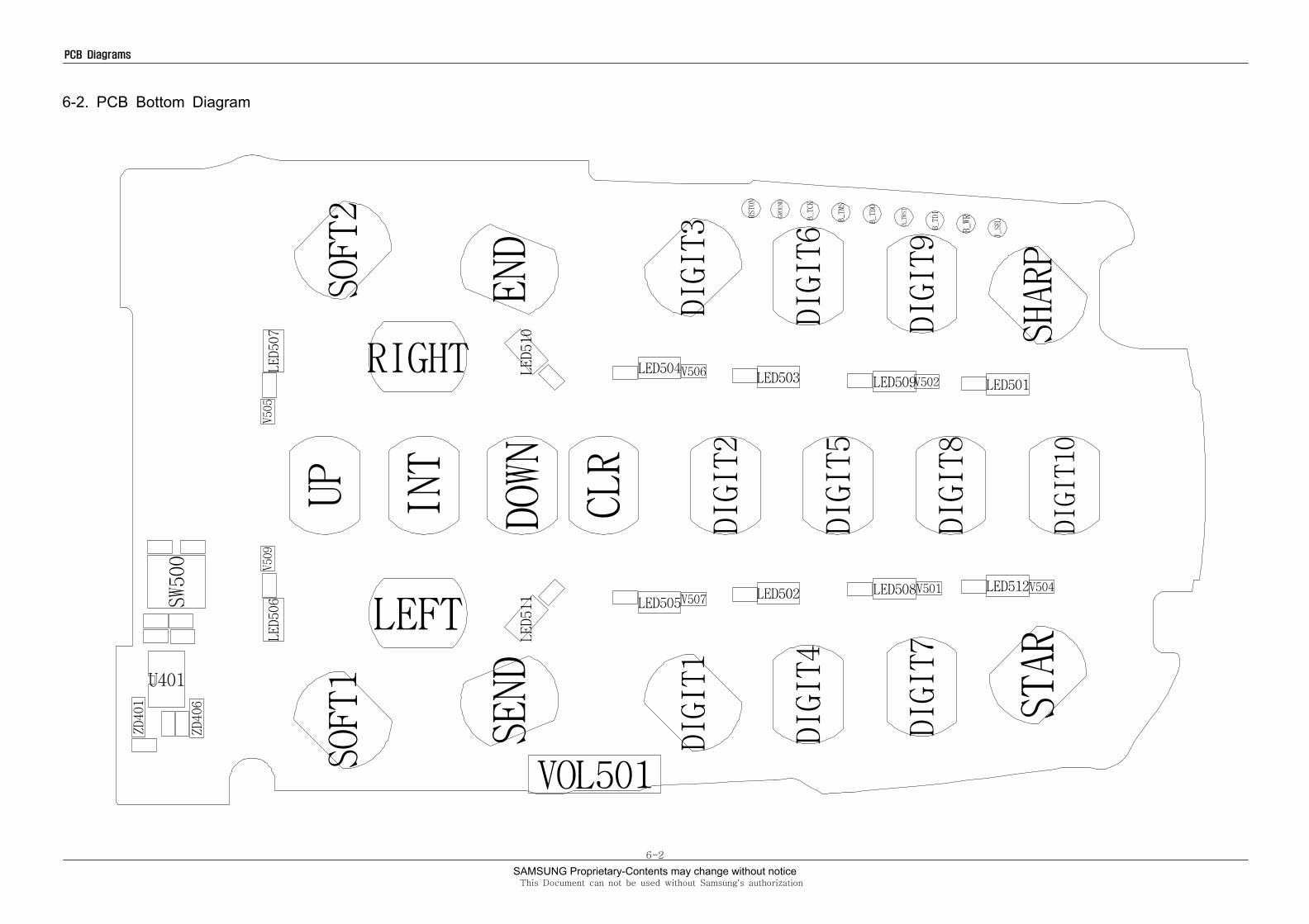
6-2. PCB Bottom Diagram

SAMSUNG Proprietary-Contents may change without notice
7. Flow Chart of Troubleshooting
This Document can not be used without Samsung's authorization
7-1
7-1. Power On
Check the Battery Voltageis more than 3.4V
' Power On ' does not work
Change the Battery
END
No
Yes
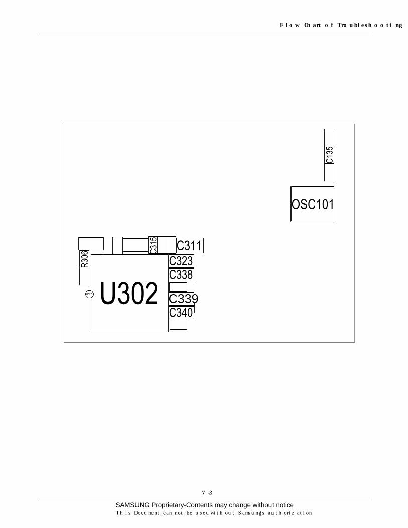
C315(V_ISUP) = 2.7V? Check the PMU related to V_ISUPNo
Yes
Check the Clock atR306=32KHZ
Resolder X300No
Yes
C340 (VDD1) = "H"? Check the VDD1 circuitNo
Yes
C339(VDD2) & C338(VDD3)= 2.85V?
Check the VDD2,VDD3 circuitNo
Yes
Check for the clock at C135= 13MHz
Check the clock generation circuit
(related to U101)
No
Yes
Check the initial operation
Yes
Yes

SAMSUNG Proprietary-Contents may change without noticeThis Document can not be used without Samsung's authorization
Flow Chart of Troubleshooting
7-2
Power On
SIM
PUMP+
BATTERY
refgnd
GE
NER
ATO
R
LINREG)
CONTROL
data
SENSOR
ON/OFF
SIM
internal
12C
PLL
VBATVOLTAGE
DV
DD
2
CLOCK
ovdd
control
32KHz XTAL
SUPPLY &
INTERFACE
SUPPLY
clocks
AV
DD
CHARGE
INTE
RR
UP
T
SUPPLYD
VD
D3
REFERENCE
HFA
(CHARGE
CONTROL
BACKLIGHT
INTERNAL
htmp
bias currents
LINREG
INTERFACEON-CHIPreference
MODULE
OSCILLATORTEMP HIGH
htm
p
POWER MANAGERMENT UNIT(PMU IC)
supply
CHARGE
&
VIB
MIC BIAScalibration
MONITOR
internal
DV
DD
1
HIGH VOLTAGE
CLOCKvoltage
PUMP
DV
DD
4
REAL-TIME
CONTROL
status
GENERATOR
SWITCH
C323
VCC_SYN_2V7
AVDD_2V65
VBAT
VBAT
C324
C305
VDD_VIB_3V05
BLVDD_3V25
VDD3_2V85
C339
C320
TP300
CLOCK6
GND2
IO1
NC5
3 SIM VCC 4
VDD2_2V85
BAT300
VBAT
U301
C337
C309
VDD1_1V8
VCC_RX_TX_2V7
VCC_RF_VCO_2V7
V_ISUP_2V5
C310
C316
C318
C341
C314
C322
C336
VBAT
VBAT
21
VDD1_1V8
R301
CC7V-T1AX300
C328
TP301
C315
VCC_TX_BURST_2V7
C326 C330
C333
C313
R305
C335
V_ISUP_2V5
L300
C329C327
C302
MIC_BIAS_2V1
C338
C325
C340
AVDD_TEMP_2V65
C321
VBATVDD_KEY_2V95
C301
C312
34 45566
7GG
89GG
10
G6
VCC_CP_4V
CN300
1122
3
D4
VSS
20VS
S21
C4F4
VSS
3
G4
VSS
4VS
S5
J3 G5
VSS
6VS
S7
K5F6
VSS
8VS
S9
E6 E7
VSS
14VS
S15
D7C7
VSS
16
D6
VSS
17
E5
VSS
18VS
S19
D5F5
VSS
2
C2VCC
VIB
VBA
T
B3 A3
VIB
VDD
H7
VPR
OG
VSS
1
E4 G7
VSS
10VS
S11
G8F7
VSS
12VS
S13
B8
A1
SIM
SC
N
B1
SIM
SC
P
B2
SIM
VB
AT
SLP
MO
D
D10H5
TM
VBACKJ5K4 VBAT
C1
RST
O
D9
E3 SCLF2 SDA
SEL
12R
B
E9 H4
SEL
3RB
C6SIMCLK
A2
SIM
GN
D
SIMIO
E8
G10 RF1VDD
F9RF1VDDS
H9 RF2SNS
RF2SWSE10
H10 RF2VDD
J10RF2VDDS
G9 RFVBAT
RST
OSC32I K8
OSC32O K9
K1
REC
1
J2
RE
C2
K2
REC
3
H8 REFCK6 REFGND
F10 RF1SNS
RF1SWS
C10
D2IO
H6ISUPAJ4ISUPD
MICBIASJ6
1NC
2NC
ON
KEY
H3
HFA
VD
DA6B6
HFA
VD
D
B9HVSGND
B10HVSOCHVSSCN A10
C9HVSSCP
C8HVSVBAT
D8HVSVDD
INT
H1
DVD
D3
DVD
D3
J1H2
DVD
D3V
BA
T
A4
DVD
D4
DVD
D4O
N
F8 B4
DVD
D4V
BA
T
A5H
FAV
BA
TH
FAV
BA
TB5
C3CLK
A9
CLK
32
D1CPRES
F1
DVD
D1
DVD
D1V
BA
T
F3 G2
DVD
D2
DVD
D2
G1G3
DVD
D2V
BA
T
J9
A8 BBMGND
C5BBMSW
B7BLVBATA7 BLVDD
E1CHRIVCHRREG E2
D3CHRVBAT
AU
XO
N
K3
AVD
D
J7 K7
AVD
D
AVD
DS
K10J8
AVD
DV
BA
TA
VDD
VB
AT
C332
U302
C311
R306
C334
32K
CHARGER_OK
PON_SYNT
PON_TX
SDASCL
BACKLIGHT
VIB
BLVDD_3V25
SIMCLKSIMIO
REF_ON
RSTON
JIG_REC
JACK_INRECO1
ONKEY_N
IT_PMU
SAMSUNG Proprietary-Contents may change without notice
Flow Chart of Troubleshooting
This Document can not be used without Samsung's authorization
7-3
C339

SAMSUNG Proprietary-Contents may change without noticeThis Document can not be used without Samsung's authorization
Flow Chart of Troubleshooting
7-4
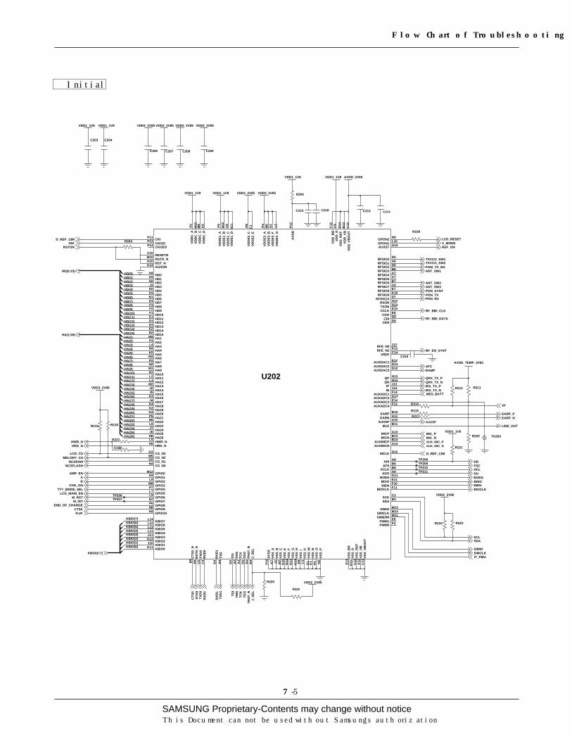
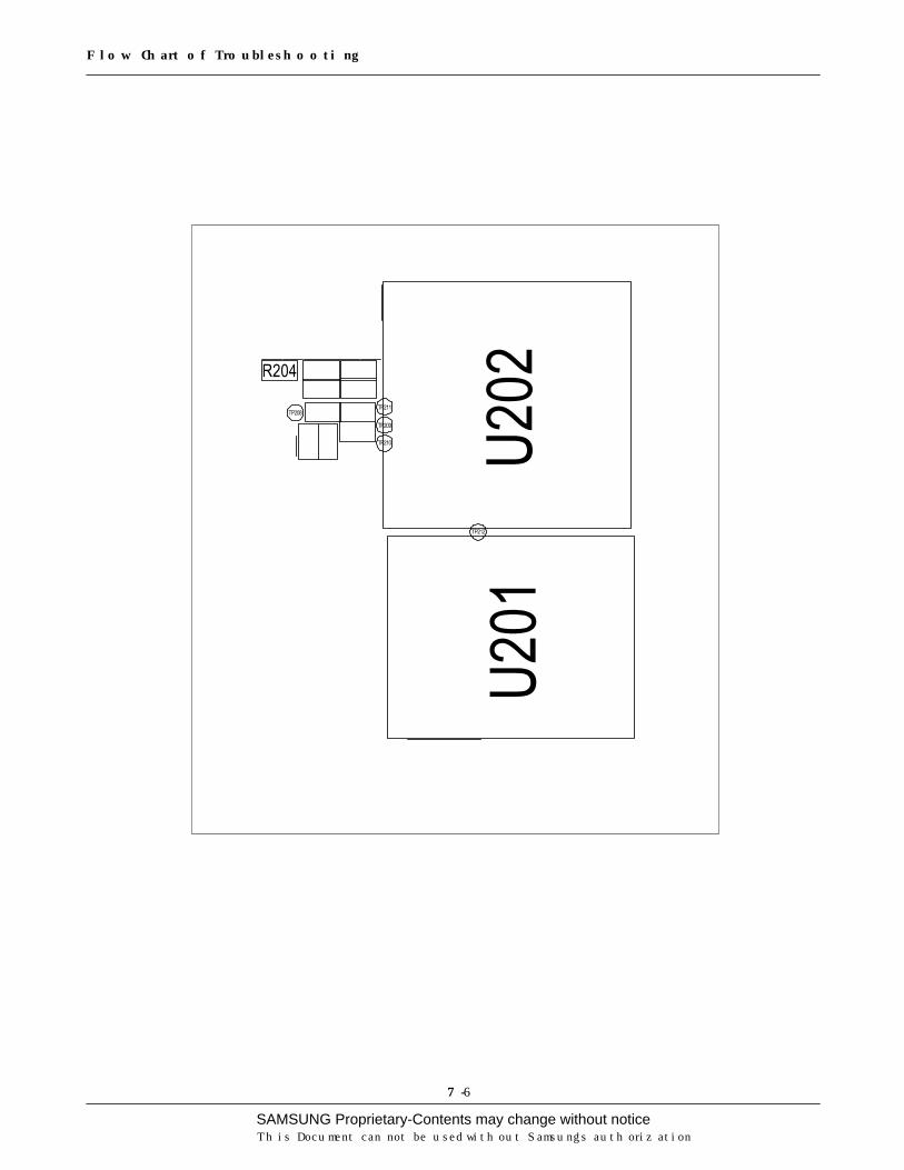
7-2. Initial
R204 (RSTON) ="H"?
Initial Failure
Check the circuit related to reset
END
No
Yes
Is U201 Pin(memory CE) OK?
Yes
Yes
No
Check the U201
Check the circuit aroundLCD & U201 (Short or not solder)
Yes
SAMSUNG Proprietary-Contents may change without notice
Flow Chart of Troubleshooting
This Document can not be used without Samsung's authorization
7-5
Initial
R218
VDD3_2V85
C207
R219
VDD1_1V8
VDD2_2V85
VDD1_1V8
R223
VSS_
NK
1
VSS_
OP1 N
5VS
S_P
C13
VSS_
REF
A12
VSS_
VBC
11VS
S_VB
OU
T
C206
M7
D11
VSS_
D
N10
VSS_
EN
14VS
S_F
N11
VSS_
GVS
S_H
G13 E8
VSS_
IC
3VS
S_K
G1
VSS_
M
C9
D14
VDD
_REF
VDD
_VB
B12
C12
VDD
_VB
OU
TC14VREF
K7
VSS_
AJ1
VSS_
B
E13
VSS_
BB
VSS_
C
H11
VDD
E2_C
P8
VDD
E2_E
C1
VDD
E3_A
P4
VDD
E3_B
M6
VDD
E3_F
G2 L3
VDD
E3_G
F12
VDD
_BB
VDD
_D
F5VD
DC
_AN
13VD
DC
_BM
8VD
DC
_CK
6VD
DC
_D
P9VD
DE1
_AN
12VD
DE1
_BVD
DE1
_CC
8VD
DE1
_D
A3
TCK
D2
TDI
TDO
D3
TMS
A2
A1
TRST
_N
C5
TXD
0
TXD
A4
G12TXON
C4
RXD
0
D4
RXD
1
H12RXON
C2SCKSDA B3
SIMCLK M14
SIMERR M11
M13SIMIO
RFSIG5 C7B7RFSIG6
RFSIG7 C6E7RFSIG8
RFSIG9 K10
M10 RSTO_NRST_NH10
RXT
0_N
A5
C10
J12RFE_N0 K12RFE_N2
D5RFSIG0 A6RFSIG1
RFSIG10 D7
D6RFSIG2RFSIG3 B6
A7RFSIG4
KBIO7
D10MCLK
MICN B13A13MICP
PWM0 F4E6PWM1
QN H14QP H13
RESETNJ_
SELKBIO0K11
KBIO1J10 KBIO2K13J11 KBIO3
L11 KBIO4
L13 KBIO5
L12 KBIO6
L14
E4 HD7F3 HD8
HD9F2
HRD_NH5L5 HWR_N
IN J14IP J13
B4
D1E3 HD13
HD14E2
HD15B2
H2 HD2HD3J3
HD4E5
HD5H1B1 HD6
M3
HA7P2
HA8N2M1 HA9
H4 HD0H3 HD1
HD10F1
HD11E1
HD12
HA22L6 HA23HA24J7
J6 HA25HA26H6
HA3L4
HA4N3
HA5K5
HA6
HA16K3J4 HA17
HA18K4K2 HA19
P3 HA2
G4 HA20HA21P5
N6
GPON2 N9
M4 HA1
HA10N1L2 HA11L1 HA12M2 HA13
HA14J2J5 HA15
GPIO3M9
GPIO4P7L7 GPIO5
GPIO6L9
GPIO7N7
GPIO8P6
GPIO9N8
GPON1 L10
CS_N2CS_N3G3
B5
CTS
0_N
A11EARNEARP B10
M12 GPIO0K9 GPIO1
K8 GPIO10
GPIO2L8
D8E9CDO
D9CEN
CKIP11P13 CKI32I
CKI32OP14
CS_N0N4 CS_N1G5M5
P10
AVS
S
BDIO E11
BIEN F10F11BIOCLK
BOEN G11
B11BUZ
CCLK E10
CDI
E12D13AUXDAC2 D12AUXDAC3
AUXMICN A14B14AUXMICP
K14 AUXON
AUXSP A10
AUXST G10
P12
AVD
D
ACLK
ADI A8
ADO A9
AFS B9
F14AUXADC1AUXADC2 G14
E14AUXADC3AUXADC4 F13
AUXDAC1
U202
B8
VDD1_1V8
C200
TP207
VDD2_2V85
R227
VDD2_2V85
R224
TP210
C203
R204
R214
TP206
VDD3_2V85
TP208
VDD1_1V8
R225
C219
R211
R217
TP209
TH200
VDD1_1V8
VDD3_2V85
VDD2_2V85
R228
R221
AVDD_TEMP_2V65
C204
TP211
R220
C213
AVDD_2V65
VDD2_2V85
VDD1_1V8 VDD1_1V8
C214
R200
C229
R212
C208
C216C215
R215
HWR_N
VDD2_2V85
R226
TTY_MODE_SEL
LCD_RESET
FLIP
VF
EARP_NEARP_P
AUXSP
AUX_MIC_PAUX_MIC_N
HA(10)HA(9)HA(8)HA(7)HA(6)HA(5)HA(4)
HD(15)HD(14)HD(13)HD(12)HD(11)HD(10)HD(9)HD(8)HD(7)HD(6)HD(5)HD(4)HD(3)HD(2)HD(1)HD(0)
HD(0:15)
AMP_EN
KBIO(2)KBIO(3)KBIO(4)KBIO(5)KBIO(6)KBIO(7)
KBIO(0:7)
HA(22)HA(21)HA(20)HA(19)HA(18)HA(17)HA(16)HA(15)HA(14)HA(13)HA(12)HA(11)
SDA
RXD
0TX
D0
CTS
0
BIENBDIOBOEN
BIOCLK
ANT_SW2
PON_SYNTPON_TX
NCSRAMMELODY_CS
HRD_N
RSTON
D_REF_13M
KBIO(0)KBIO(1)
D_REF_13M
RAMPAFC
32K
TXD
1
TRST
_N
TMS
TDO
TDI
TCK
RXD
1
RTS
0
J_SE
LREF_ON
CTS0
SIMCLKSIMIO
IT_PMU
SCL
MES_BATT
LCD_CS
CHG_ON
END_OF_CHARGE
A
FSC
DUDCL
DD
MIC_NMIC_P
IRX_TX_NIRX_TX_PQRX_TX_NQRX_TX_P
V_MODE
HA(26)HA(25)HA(24)
ANT_SW3
TXVCO_SW1
NCSFLASH
ANT_SW1PAM_TX_EN
PON_RX
RF_EN_SYNT
HA(3)
HA(23)
HA(2)HA(1)
RF_BBI_DATA
RF_BBI_CLK
LINE_OUT
M_RSTLCD_MAIN_EN
M_INT
B
TXVCO_SW2
HA(1:26)
SAMSUNG Proprietary-Contents may change without noticeThis Document can not be used without Samsung's authorization
Flow Chart of Troubleshooting
7-6

SAMSUNG Proprietary-Contents may change without notice
Flow Chart of Troubleshooting
This Document can not be used without Samsung's authorization
7-7
7-3. Charging Part
Check the U300 pin 2> 4.9V
Abnormal charging part
END
No
Yes
U300 pin 4 = "H"?No
Yes
Check the C300≒ 4.2V
No
Yes
Check the the circuit related to
+DCVOLT
Resolder or replace U300
Check the circuit related to
CHG_ON signal
Yes
U300 pin 5 = "L"?
Yes
No
Resolder or replace U300

SAMSUNG Proprietary-Contents may change without noticeThis Document can not be used without Samsung's authorization
Flow Chart of Troubleshooting
7-8
Charging
CHARGER IC
R302
R303
VDD2_2V85VBAT
C306
UD
ZS8.
2B
+DCVOLT_5V
C307
R300
C308
C300
C303C304
R30
4
12G
3 GND
IN2
ISET4
1 VL
6_ACOK
_CHG 8
5_EN
U300
7BATT
9G
10GG
11
MES_BATT
CHARGER_OK
END_OF_CHARGE
CHG_ON

SAMSUNG Proprietary-Contents may change without notice
Flow Chart of Troubleshooting
This Document can not be used without Samsung's authorization
7-9

SAMSUNG Proprietary-Contents may change without noticeThis Document can not be used without Samsung's authorization
Flow Chart of Troubleshooting
7-10
7-4. Sim Part
CN300 pin 1,5 = "H"?
Phone can't access SIM Card
Check the sim charge pump
Check the SIM Card
END
No
Yes
Yes
Yes
No
Check the 32k OSCAfter Power ON,
Check SIMCLK Signal onCN300 pin3 in a few second
Yes
No
Replace PBAAfter SIM card insert,
CN300 pin 2 = "H(SIM_RST)"?
Yes

SAMSUNG Proprietary-Contents may change without notice
Flow Chart of Troubleshooting
This Document can not be used without Samsung's authorization
7-11
7-5. Microphone Part
Check the connectionfrom MIC
Check the circuitfrom U202 to MIC
Resolder MIC
Resolder the R400, R401, R404, R407,
L400, L401, C408 and C412
END
No
Yes
Yes
Yes
Yes
No
Check the MIC
No
Replace the MIC
Microphone does not work

SAMSUNG Proprietary-Contents may change without noticeThis Document can not be used without Samsung's authorization
Flow Chart of Troubleshooting
7-12
Close to MCPClose to microphone
MICROPHONER400
C405
C412
VDD2_2V85
MIC_BIAS_2V1
R401C407
V402
C400
C414C411
V401
5
6
7
R409
U401-2
C418
R416
L401
VDD2_2V85
C408
R415
R404
C406
C417
R412
VDD2_2V85
R402
L400
2
81
U401-14
3
C416
C413
R407
M400
MIC+
MIC_P
MIC_N
JACK_INEAR_SWITCH
Microphone
SAMSUNG Proprietary-Contents may change without notice
Flow Chart of Troubleshooting
This Document can not be used without Samsung's authorization
7-13
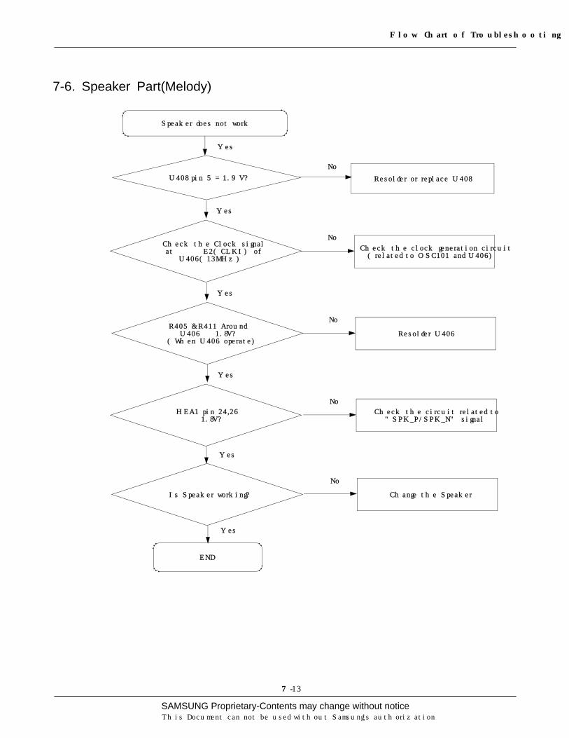
7-6. Speaker Part(Melody)
U408 pin 5 = 1.9V?
Speaker does not work
Check the Clock signalat E2(CLKI) ofU406(13MHz)
Check the clock generation circuit(related to OSC101 and U406)
END
No
Yes
No
Resolder or replace U408
R405 & R411 AroundU406 ≒ 1.8V?
(When U406 operate)Resolder U406
Yes
No
HEA1 pin 24,26≒ 1.8V?
Check the circuit related to"SPK_P/SPK_N" signal
Yes
No
Is Speaker working?
No
Yes
Change the Speaker
Yes
Yes

SAMSUNG Proprietary-Contents may change without noticeThis Document can not be used without Samsung's authorization
Flow Chart of Troubleshooting
7-14
Speaker
MELODY IC
VDD_1.9V
R411
C422
C401
R410
C402
R414
C439
VDD3_2V85
R403/WR,SCKJ5
J6 SO
LED2 J7
MTR J8
H5SMODE
GPIOH6
LED1H7LED0 H8
J1 D4
D1J2
J3 DVDDJ4DVSS
G5 IFSEL
TESTI2 G6
G7 MTR
BCLKG8
D4H1
D2H2
IOVDD2 H3
/CS,_SSH4
D5F3
TESTI1 F6
LRCK F7
SDINF8
D6G1
D3G2
D0G3
/RD,SIG4
DVDDE1
CLKIE2
E3A1
MCLKE6
/IRQE7
IOVDD1E8
A0F1
D7F2
C8 SPVDD
DVSSD1
PLLCD2
/RSTD3
D4 INDEX
D6TESTI0
DVDDD7
DVSS D8
SPVSS B8
AVDDC1
TXOUTC2
RXIN C3
EXTINC4
BBRC5
EXTOUTC6
TESTI3C7
SPOUT1 A8
AVSS B1
VREFB2
HPCB3
EQ1B4
BBLB5
HPOUTL B6
SPOUT1B7
NC 2
A1RXIN
EXCA2
EQ2A3
EQ3A4
A5HPVSSHPOUTR A6
SPOUT2 A7
U406
YMU788
NC1
C424
VDD_1.9V
R417
R405
VDD_1.9V
C421
C420R406
R408
C409
C419
C425
C423
C403
C415
C404
C426
C410
U408
GND3
IN2
NC1
OUT 4
VCC5
R424
R413
VBATVDD2_2V85
AMP_IN
AMP_P
AMP_N
LINE_OUT
HRD_N
VIB
HD(4)
HD(2)
MELODY_CS
HD(1)
HWR_N
MEL_13M
HD(6)HD(7)
HD(5)
M_RST
HA(2)
M_INT
HA(1)
HD(3)
HD(0)

SAMSUNG Proprietary-Contents may change without notice
Flow Chart of Troubleshooting
This Document can not be used without Samsung's authorization
7-15

SAMSUNG Proprietary-Contents may change without noticeThis Document can not be used without Samsung's authorization
Flow Chart of Troubleshooting
7-16
7-7. Key Data Input
When one of the keys ispushed,
is it displayed on LCD?
Check the Dome sheet & Key rubber
END
No
Yes
Yes
Check Initial Operation
When one of the keys ispushed,
KBIO signal is OK?
Replace the PBA
No
Yes

SAMSUNG Proprietary-Contents may change without notice
Flow Chart of Troubleshooting
This Document can not be used without Samsung's authorization
7-17
7-8. Receiver Part
U402 pin 3, 15 = 1.5V? Resolder or replace U402
END
No
Yes
Yes
Receiver does not work
SPK +,- PAD = 1.5V? Change LCD module
No
Yes
Is Receiver working? Replace the Receiver
No
Yes
No
Resolder or replace U402
Yes
No
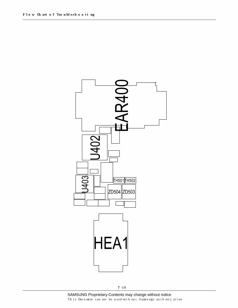
Resolder EAR400EAR400 pin 5, 2 = short?
Yes
HEA1 pin 24, 26 = 1.5V?
No
Resolder HEA1
Yes
Check the soldering of thespeaker wire
No
Modify the speaker wire soldering
Yes
U402 pin 8, 12 = 1.5?
SAMSUNG Proprietary-Contents may change without noticeThis Document can not be used without Samsung's authorization
Flow Chart of Troubleshooting
7-18

SAMSUNG Proprietary-Contents may change without notice
Flow Chart of Troubleshooting
This Document can not be used without Samsung's authorization
7-19
7-9. LCD Part (for Color Main )
Is LCD Contrast set onhigh level in the Menu?
Set LCD Contrast on high level
END
No
Yes
Yes
LCD does not work
HEA1 pin 2 = 2.8V? Check the U502
No
Yes
HEA1 pin 19(HWR_N)21(HA(1)) is OK?
Check the U202
No
Yes
Yes
Replace the LCD Module

SAMSUNG Proprietary-Contents may change without noticeThis Document can not be used without Samsung's authorization
Flow Chart of Troubleshooting
7-20
TP212

SAMSUNG Proprietary-Contents may change without notice
Flow Chart of Troubleshooting
This Document can not be used without Samsung's authorization
7-21
7-10. Key Back Light
C333 = "H"? Check the PMU related to "VDD_KEY"
END
No
Yes
Key Backlight does not work
Yes
SAMSUNG Proprietary-Contents may change without noticeThis Document can not be used without Samsung's authorization
Flow Chart of Troubleshooting
7-22
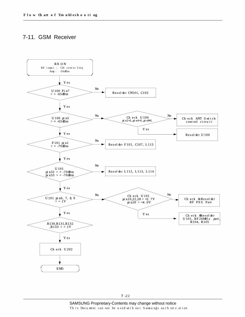
7-11. GSM Receiver
U100 Pin7>= -65dBm Resolder CN101, C102
END
No
Yes
RX ONRF input : CH center freq
Amp : -50dBm
Check U100pin2=L,pin4=L,pin8=L
U100 pin5>= -65dBm
F101 pin1>= -70dBm
U101 pin6, 7, 8, 9>= 1V
U101pin32 >= -70dBmpin33 >= -70dBm
Check ANT Switchcontrol circuit
Resolder U100
Resolder F101, C107, L115
Resolder L112, L113, L114
Check U101pin10,22,28 >=2.7Vpin20 >=4.0V
Check & ResolderRF PSU Part
Check &ResolderU101, RF26MHz part,
R104, R105R130,R131,R132,R133 >= 1V
Yes
Yes
Yes
Yes
Yes
Yes
Yes
Yes
No
No
No
No No
No
Check U202

SAMSUNG Proprietary-Contents may change without notice
Flow Chart of Troubleshooting
This Document can not be used without Samsung's authorization
7-23

SAMSUNG Proprietary-Contents may change without noticeThis Document can not be used without Samsung's authorization
Flow Chart of Troubleshooting
7-24
7-12. GSM Transmitter
TX ON (5Level)
U100 Pin7>= 20dBm
U100 Pin11>= 20dBm
U102 Pin6>= 20dBm
U102 Pin48>= 3dBm
OSC100 pin1>= 6Bm
U101 Pin6, 7, 8, 9>= 500mV
Resolder CN101, C102
Check U100pin2=L,pin4=H,pin8=L
Resolder C119, L117
Check U101pin4 >= 4.0V
pin22, 28 >= 2.7V
Changeor Resolder U100
Check ANT Switchcontrol circuit
Check & ResolderRF PSU part
Resolder U101or check Txcpo(R129)
Yes
No
Yes
Yes
Yes
Yes
Yes
Yes
No
No
No
No
No
No
No
Check U102+VBATT(pin42,43)
OK?
Resolder or change U102or check PAM control
signal
Check +VBATT
Yes
No
Resolder R107, R111, R112
Yes
Check U202
END

SAMSUNG Proprietary-Contents may change without notice
Flow Chart of Troubleshooting
This Document can not be used without Samsung's authorization
7-25

SAMSUNG Proprietary-Contents may change without noticeThis Document can not be used without Samsung's authorization
Flow Chart of Troubleshooting
7-26
7-13. DCS Receiver
RX ONRF input : CH center freq
Amp : -50dBm
U100 Pin7>= -65dBm
U100 pin1>= -65dBm
F102 pin1>= -70dBm
U101Pin38>=-70dBmPin39>=-70dBm
U101 pin6, 7, 8, 9>= 1V
R130,R131,R132,R133 >= 1V
Check U202
END
Resolder CN101, C102
Check U100pin2=L,pin4=L,pin8=L
Check ANT Switchcontrol circuit
Resolder U100
No
Yes
Resolder F102, C104, L111
Resolder L105, L106, L108
Check U101pin22,28 >= 2.7Vpin4 >= 4.0V
Check & ResolderRF PSU Part
Check & ResolderU101, RF26MHz part
R104, R105
Yes
Yes
Yes
Yes
Yes
Yes
Yes
No No
No
No
No No
Yes

SAMSUNG Proprietary-Contents may change without notice
Flow Chart of Troubleshooting
This Document can not be used without Samsung's authorization
7-27

SAMSUNG Proprietary-Contents may change without noticeThis Document can not be used without Samsung's authorization
Flow Chart of Troubleshooting
7-28
7-14. DCS Transmitter
TX ON (0Level)
Resolder C117, L116
Check ANT Switchcontrol circuit
Changeor Resolder U100
Check U100pin2=L,pin4=L,pin8=H
YesResolder CN101, C102
END
Check U202
U101 Pin6, 7, 8, 9>= 500mV
OSC100 pin2>= 6Bm
U102 Pin37>= 3dBm
U102 Pin31>= 20dBm
U100 Pin9>= 20dBm
U100 Pin7>= 20dBm
Resolder U101or check Txcpo(R129)
Check & ResolderRF PSU part
Check U101pin4 >= 4.0V
pin22, 28 >= 2.7V
Resolder R115, R120, R121
No
Yes
Yes
Yes
Check U102+VBATT(pin42,43)
OK?
Resolder or change U102or check PAM control
signal
Check +VBATT
No
No
No
No
No
Yes
Yes
Yes Yes
Yes
No
No
No

SAMSUNG Proprietary-Contents may change without notice
Flow Chart of Troubleshooting
This Document can not be used without Samsung's authorization
7-29

SAMSUNG Proprietary-Contents may change without noticeThis Document can not be used without Samsung's authorization
Flow Chart of Troubleshooting
7-30
7-15. PCS Receiver
RX ONRF input : CH center freq
Amp : -50dBm
Resolder F100, C103, L104
Check ANT Switchcontrol circuit
Changeor Resolder U100
Check U100pin2=H,pin4=L,pin8=L
Resolder CN101, C102
END
Check U202
R130,R131,R132,R133 >= 1V
U101 Pin 6,7,8,9>= 1V
U101 Pin35,36>= -70dBm
F100 Pin1>= -70dBm
U100 Pin3>= -65dBm
U100 Pin7>= -65dBm
Check & ResolderU101, RF 26MHz part,
R104, R105
Check & ResolderRF PSU part
Check U101pin4 >= 4.0V
pin22, 28 >= 2.7V
Resolder L101, L102, L103
Yes
No
Yes
Yes
Yes
Yes
Yes
Yes
No
No
No
No
No
Yes

SAMSUNG Proprietary-Contents may change without notice
Flow Chart of Troubleshooting
This Document can not be used without Samsung's authorization
7-31

SAMSUNG Proprietary-Contents may change without noticeThis Document can not be used without Samsung's authorization
Flow Chart of Troubleshooting
7-32
7-16. PCS Transmitter
TX ON (0Level)
Resolder U101or check Txcpo(R129)
Check & ResolderRF PSU part
Check U101pin4 >= 4.0V
pin22, 28 >= 2.7V
Resolder R115, R120, R121
Check +VBATT
Check U102+VBATT(pin42,43)
OK?
Resolder or change U102or check PAM control
signal
Resolder C117, L116
Check ANT Switchcontrol circuit
Changeor Resolder U100
Check U100pin2=L,pin4=L,pin8=H
YesResolder CN101, C102
END
Check U202
U101 Pin6, 7, 8, 9>= 500mV
OSC100 pin2>= 6Bm
U102 Pin37>= 3dBm
U102 Pin31>= 20dBm
U100 Pin9>= 20dBm
U100 Pin7>= 20dBm
No
No
No
No
No
No
Yes
Yes
Yes
Yes
Yes Yes
Yes
Yes
No
No
No

SAMSUNG Proprietary-Contents may change without notice
Flow Chart of Troubleshooting
This Document can not be used without Samsung's authorization
7-33

SAMSUNG Proprietary-Contents may change without noticeThis Document can not be used without Samsung's authorization
Flow Chart of Troubleshooting
7-34
Transmitter & Receiver
L
L
LD
CS/
PCS
TxH
_EC
OS
L
VC1
L
VC3
L L
LL
H
LLD
CS
Rx
GSM
850
/900
Tx
L
PCS
Rx
H
GSM
Rx
VC2
C10
1
C10
8
R10
5
C11
5
C15
8
R11
2
L102
L103
C11
2
1O
UT1
OU
T25
11
VCC17
VCC2
C15
7
GN
D2 4
BA
ND
9C
ON
TRO
L
3
BANDGND
6
GND
810
GNDGND
12
L108
OS
C10
0
R12
0C
134
C13
8
R12
3
C12
0
C11
9
R11
7
C12
2
C12
7
C15
6
C15
2
AN
T2
C14
4
L110
C11
0
L118
R11
4
F100
B78
51
2GG
5
IN1
3O
UT
OU
T4
C12
9
R13
3
C12
51N
F50
V
C14
3
C10
3
R10
2
C13
7
L115
C11
1C
109
R13
2
L105
R10
1L1
19
R13
6
R13
4
C14
7
R11
8
R10
6
R10
9
C12
1
C13
6
C11
7
C10
5
C13
0
0R
108
R12
8
B78
45
2GG
5
1IN
OU
T3 4
OU
T
F101
C10
4
R12
1
R12
922K
,1%
C15
4
R11
6R
115
R13
5
L101
L113
L109
GN
D
OU
T34
VCC
1VC
ON
R12
2
OSC
101
2
C13
5
R11
0
R12
5
C12
41U
F10
V
R11
3
4O
UT
C14
5
B78
52F1
02
2GG
5
1IN
3O
UT
C15
5
L111
L107
C1
6
C2
3
E1
1
E2
4
AN
T1
L104
Q10
0
PEM
D10
B1
2
B2
5
C11
4L1
16
C13
1
C10
6
1.8N
FC
116
C15
3
50V
R12
6
L112
R11
1
C12
6
C13
2
R12
7
C13
9
C14
1
1
TXRFI
R10
7
37R
FGN
D2
RFLOVCC28RFTUNE26
RFV
CC
3125 RFVCOVCC
RXON2324 SYNON
22 SYNVCC
TXCPO
3
TXCPVCC
45
TXON
4635PC
SIA
36PC
SIB
8
QA
QB
9
REF
GN
D1415
REF
IN
REF
VCC
16
RFCPO21
20R
FCPV
CC
34R
FGN
D1
GN
D2
42 43G
ND
3G
ND
444
27 GNDTUNE32
GSM
IA
33G
SMIB
6
IA
7
IB
IFVCC10
45N
C1
NC
2
CLK
FDB
X
11C
LKO
UT
DA
TA17
38D
CSI
A
39D
CSI
B
EN19
EXTRES
2
FESW12930 FESW2
40FE
SWO
N
41GND1
U10
1
12C
AFC
SUP
18C
LK
13
R12
4
VCC3DCS/PCS2118VCC3GSM
VCCOUT19
VCCOUT20
VRAMP45
NC15
TXENABLE41
VBATT4243 VBATT
VCC139
VCC1GSM46
VCC
2DC
S/PC
S35
VCC
2GSM
2
NC38
NC44
NC
9
NC
10
NC
11
NC
12
NC13
NC14
NC
25N
C26
NC
2728N
C
NC
29
NC
8
NC
33
NC
36
GSM
850/
900O
UT
6
GSM
INTE
RG
ND
1
NC
3
NC16
NC17
NC22
NC23
NC24
7G
ND
GN
D30
GN
D3234
GN
D
49 GND
50 GNDGND51
GSM850/900IN48
DCS/PCSIN37
DC
S/PC
SOU
T31
GN
D4GND52
GN
D53
GN
D54
GND1GSM47
GN
D5
U10
2
BANDSEL40
C13
3
L106
C14
0
C12
3
KM
S-5
12
2A
C 3
G 1
G4
C10
2
CO
N10
1
R10
4
C14
6
100K
C14
2
R11
9
C10
7
C11
3
C11
8
R13
0
L117
C12
8
G5
1314
G6G
SM_R
X5
GSM
_TX
113
PCS_
RX
4VC
1VC
28 2
VC3
U10
0
AN
T7
1D
CS_
RX
DC
S|PC
S_T
9
6
G2G
3
10
G4
12
R13
1
VCC
_CP_
4V
L114
VCC
_RX_
TX_2
V7
FE_S
W1
FE_S
W2
AN
T
FE_S
W1
FE_S
W2
VCC
_SYN
_2V7
PON
_TX
IRX_
TX_P
IRX_
TX_N
QR
X_TX
_P
QR
X_TX
_N
MEL
_13M
VB
AT
PCS_
RX
AN
T_SW
2
AN
T_SW
1
PCS_
RX
AN
T_S
W3
PA
M_T
X_E
N
RA
MP
TXVC
O_S
W1
TXVC
O_S
W2
VCC
_TX_
BU
RST
_2V7
AFC
D_R
EF_1
3M
RF_
BB
I_C
LK
RF_
BB
I_D
ATA
RF_
EN_S
YNT
VCC
_CP_
4V
VCC
_RF_
VCO
_2V7
VCC
_RX_
TX_2
V7
PON
_RX
PON
_SYN
T
VCC
_SYN
_2V7