Embed Size (px)
Citation preview

CDCE906/CDCE706 PerformanceEvaluation Module
User's Guide
August 2007 High Performance Analog/CDC
SCAU016B

2 SCAU016B–August 2006–Revised August 2007Submit Documentation Feedback

Contents
1 Introduction................................................................................................................ 52 Quick Start ................................................................................................................. 83 EVM Hardware ............................................................................................................ 9
3.1 Board View and Connector Location .......................................................................... 9
3.2 Hardware Configuration ......................................................................................... 9
4 TI Pro-Clock™........................................................................................................... 114.1 CDCE906-706 SMBus Interface.............................................................................. 11
4.2 CDCE906-706 Programming Assistant...................................................................... 12
4.3 Tutorial ........................................................................................................... 14
4.4 Software Installation............................................................................................ 15
5 FAQ ......................................................................................................................... 166 Parts List.................................................................................................................. 167 Board Layout and Schematic ...................................................................................... 18
Important Notices ............................................................................................................... 25
SCAU016B–August 2006–Revised August 2007 Table of Contents 3Submit Documentation Feedback

List of Figures
1 CDCE906/CDCE706 Functional Block Diagram......................................................................... 62 CDCE906/CDCE706 Default Setup ....................................................................................... 83 Board View ................................................................................................................... 94 CDCE906-706 SMBus Interface ......................................................................................... 115 Programming Assistant.................................................................................................... 136 Top Silkscreen .............................................................................................................. 187 Top Side ..................................................................................................................... 198 Ground....................................................................................................................... 209 Power ........................................................................................................................ 2110 Bottom Silkscreen .......................................................................................................... 2211 Schematic - Page 1 ........................................................................................................ 2312 Schematic - Page 2 ........................................................................................................ 24
List of Tables
1 Parts List .................................................................................................................... 16
4 List of Figures SCAU016B–August 2006–Revised August 2007Submit Documentation Feedback

1 Introduction
User's GuideSCAU016B–August 2006–Revised August 2007
CDCE906/CDCE706 Performance Evaluation Module
This user's guide explains how to use the CDCE906/CDCE706 performance evaluation module andprovides guidelines to build a customer's own systems. The device is soldered on the board to supportperformance measurements. The device is preprogrammed (Default Setting), but can be reprogrammedvia the parallel port to meet the customer application. There is another EVM with socket available for thepurpose of sample programming. The list below shows the four devices, which can be evaluated with theCDCE906/CDCE706 Performance Evaluation Module
- CDCE706 (EEPROM, fmax = 300 MHz, industrial temperature range)
- CDCE906 (EEPROM, fmax = 167 MHz, commercial temperature range)
- CDC706 (ROM, fmax = 300 MHz, industrial temperature range)
- CDC906 (ROM, fmax = 167 MHz, commercial temperature range)
The performance of the CDCE906 and the CDCE706 is equal, but the CDCE906 has a limited outputfrequency and temperature range for operating. Because of this, the CDCE706 is used on this board forevaluation purposes. This EVM can also be used to evaluate the generic ROM versionsCDC906/CDC706, because the functionality and performance is equal to the EEPROM versionCDCE906/CDCE706, except the EEPROM functionality.
If you need assistance with this device, email: [email protected]
The CDCE906/CDCE706 is one of the smallest and powerful PLL synthesizer / multiplier / divideravailable today. Despite its small physical outlines, the CDCE906/CDCE706 is the most flexible. It has thecapability to produce an almost independent output frequency from a given input frequency.
The input frequency can be derived from a LVCMOS, a differential input clock, or a single crystal. Theappropriate input waveform can be selected via the SMBus data interface controller.
To achieve an independent output frequency the reference divider M and the feedback divider N for eachPLL can be set to values from 1 up to 511 for the M-Divider and from 1 up to 4095 for the N-Divider. ThePLL-VCO (voltage controlled oscillator) frequency than is routed to the free programmable outputswitching matrix to any of the six outputs. The switching matrix includes an additional 7-bit post-divider(1-to-127) and an inverting logic for each output.
The deep M/N divider ratio allows the generation of zero ppm clocks from e.g., a 27-MHz reference inputfrequency.
The CDCE906/CDCE706 includes three PLLs of those one supports SSC (spread-spectrum clocking).PLL1, PLL2, and PLL3 are designed for frequencies up to 300 MHz and optimized for zero-ppmapplications with wide divider factors.
PLL2 also supports center-spread and down-spread spectrum clocking (SSC). This is a proven method toeffectively reduce the energy for the selected frequency range. The electro-magnetic interference (EMI)will be significantly reduced. Also, the slew-rate controllable (SRC) output edges minimize EMI noise.
Based on the PLL frequency and the divider settings, the internal loop filter components will beautomatically adjusted to achieve high stability and optimized jitter transfer characteristic of the PLL.
SCAU016B–August 2006–Revised August 2007 CDCE906/CDCE706 Performance Evaluation Module 5Submit Documentation Feedback

www.ti.com
CLK_IN0
CLK_IN1
Factory Prg.
PLL1
MUX
MUX
prg. 9 BitDivider M
prg. 9 BitDivider M
MUX
prg. 9 BitDivider M
PLL3
PFD
Filter
VCO
PLL2 w/ SSC
PFDFilterVCO
SSC
prg. 12 BitDivider N
prg. 12 BitDivider N
prg. 12 BitDivider N
SO/AO/CLK_SEL
S1/A1
SCLOCK
Output Switch Matrix
PLL Bypass
Y4
LVCMOS
LVCMOS
Y3
Y2
LVCMOS
LVCMOS
Y1
Y0
LVCMOS
LVCMOS
EEPROMLOGIC
Y5
PFD
Filter
VCO
SDATA
XO or
2 LVCMOSor
DifferentialInput
VCC GND VCCOUT1
GND VCCOUT2
Cry
stal
or
Clo
ck In
put
14 p
F14
pF
5 x
6 P
rogr
amm
able
Sw
itch
A
6 x
Pro
gram
mab
le 7
-Bit
Div
ider
P0,
P1,
P2,
P3,
P4,
P5,
and
Inve
rsio
n Lo
gic
6 x
6 P
rogr
amm
able
Sw
itch
B
Introduction
The device supports non-volatile EEPROM programming for easy customized applications. It ispre-programmed with a factory default configuration (see Figure 2) and can be re-programmed to adifferent application configuration before it goes onto the PCB or re-programmed by in-systemprogramming. A different register setting is programmed via the serial SMBus interface.
Two free programmable inputs, S0 and S1, can be used to control for each application the mostdemanding logic control settings (outputs disable to low, outputs 3-state, power down, PLL bypass, etc).
The CDCE906/CDCE706 has three power supply pins, VCC, VCCOUT1, and VCCOUT2. VCC is thepower supply for the device. It operates from a single 3.3-V supply voltage. VCCOUT1 and VCCOUT2 arethe power supply pins for the outputs. VCCOUT1 supplies the outputs Y0 and Y1 and VCCOUT2 suppliesthe outputs Y2, Y3, Y4, and Y5. Both outputs supplies can be 2.3 V to 3.6 V. The output works even at1.7V VCCOUT. However, some limitations apply at VCCOUT below 2.3V.
The CDCE906/CDCE706 is characterized for operation from 0°C to 70°C/–40°C to 85°C.
Figure 1. CDCE906/CDCE706 Functional Block Diagram
CDCE906/CDCE706 Performance Evaluation Module6 SCAU016B–August 2006–Revised August 2007Submit Documentation Feedback

www.ti.com
Introduction
Related Documentation From Texas Instruments• CDCE906, Programmable 3-PLL Clock Synthesizer/Multiplier/Divider data sheet (SCAS814)
• CDCE706, Programmable 3-PLL Clock Synthesizer/Multiplier/Divider data sheet (SCAS815)
SCAU016B–August 2006–Revised August 2007 CDCE906/CDCE706 Performance Evaluation Module 7Submit Documentation Feedback
www.ti.com
2 Quick Start
SO/AO/CLK_SEL
S1/A1
SCLOCK
Output Switch Matrix
27 MHz
SDATA
f = 216 MHzVCO1
f = 250 MHzVCO2
f = 225.792 MHzVCO3
CLK_IN0
CLK_IN1
27-MHz
Crystal
14 pF
14 pF
Y5
Y4
Y3
Y2
Y1
Y0
27 MHz
27 MHz
27 MHz
27 MHz
27 MHz
P2-Div
8
P3-Div
9
P4-Div
32
P5-Div
4
LV
CMOS
LV
CMOS
LV
CMOS
LV
CMOS
LV
CMOS
LV
CMOS
Divider M
27
Divider M
375
Divider N
250
Divider N
3136
SSC-OFF
PLL1
PLL3
PLL2
w/ SSC
XO
or
2 LVCMOS
or
Differential
Input
EEPROM
LOGIC
SMBUS
LOGIC
PFDFilterVCO
PFDFilterVCO
PFDFilterVCO
Divider M
1
Divider N
8
MUX
P0-Div
10
P1-Div
20
MUX
MUX
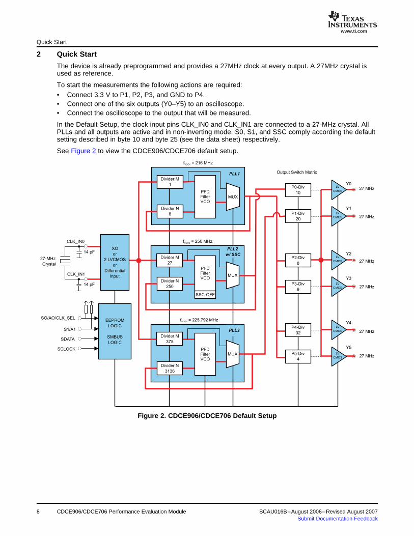
Quick Start
The device is already preprogrammed and provides a 27MHz clock at every output. A 27MHz crystal isused as reference.
To start the measurements the following actions are required:
• Connect 3.3 V to P1, P2, P3, and GND to P4.• Connect one of the six outputs (Y0–Y5) to an oscilloscope.• Connect the oscilloscope to the output that will be measured.
In the Default Setup, the clock input pins CLK_IN0 and CLK_IN1 are connected to a 27-MHz crystal. AllPLLs and all outputs are active and in non-inverting mode. S0, S1, and SSC comply according the defaultsetting described in byte 10 and byte 25 (see the data sheet) respectively.
See Figure 2 to view the CDCE906/CDCE706 default setup.
Figure 2. CDCE906/CDCE706 Default Setup
CDCE906/CDCE706 Performance Evaluation Module8 SCAU016B–August 2006–Revised August 2007Submit Documentation Feedback

www.ti.com
3 EVM Hardware
3.1 Board View and Connector Location
GND (P4)
VCC (P3)
VCC Y0-Y1 (P2)
VCC Y2-Y5 (P1)
Parallel Port
(J18)
CDCE706
SMA connector for Y0 – Y5
connector for single/differential ended input clock
(J3, J6)
27 MHz Crystal
TSX-3225 (Y1)
S1 S0
SN74LV125
J17
3.2 Hardware Configuration
3.2.1 Power Supply (P1, P2, P3, P4)
3.2.2 Onboard Jumper (J12 and J10)
EVM Hardware
Figure 3. Board View
This section describes the board configuration using on-board jumpers and solder-bridges as well as theSMBUS interface.
Use a stabilized external power supply for the EVM board.
• Supply 3.3 V ± 0.3 V on P3 for chip operation.• Supply 2.3 V – 3.6 V on P2 to supply the outputs Y0 and Y1.• Supply 2.3 V – 3.6 V on P1 to supply the outputs Y2–Y5.• Connect GND to P4.
WARNINGNever supply more than 3.6 V on P1, P2, or P3.
Use Jumper J10 to set the user programmable control input S0 to low or high.
Use Jumper J12 to set the user programmable control input S1 to low or high.
Default setting: J12 and J10 are not used.
Note: S0 and S1 are logic high due to their internal pull-up resistors if J10 and J12 are not used.
SCAU016B–August 2006–Revised August 2007 CDCE906/CDCE706 Performance Evaluation Module 9Submit Documentation Feedback

www.ti.com
3.2.3 Programming Interfaces (J18, J17)
3.2.4 Flexible Crystal, Differential or LVCMOS Input (J3, J6)
3.2.5 LVCMOS Outputs (Y0 –Y5)
EVM Hardware
To enhance the flexibility and function of the clock synthesizer, a two-signal serial interface is provided. Itfollows the SMBus specification Version 2.0, which is based upon the principals of operation of I2C. Moredetails of the SMBus specification can be found at http://www.smbus.org.
Through the SMBus, various device functions, such as individual clock output buffers, can be individuallyenabled or disabled. The registers associated with the SMBus data interface initialize to their defaultsetting, written in the EEPROM, upon power-up and therefore using this interface is optional. Clock deviceregister changes are normally made upon system initialization, if any are required. There are two ways toprogram the device externally.
• Connect the parallel port cable to PC and EVM parallel port. This needs the TI Pro Clock™ Software(see section 4).
• By external pattern generator connected to J17 (it is not possible to detect an acknowledge at J17)
Note: The shield of the parallel cable should be connected to both cable plugs.
The CDCE906/CDCE706 can use a crystal, a differential clock, or a single-ended clock as reference. Thedefault setting is a 27MHz crystal.
For a differential or a single-ended clock R2, R4, R5, and R6 must be assembled with 100 Ω, pin 2 and 3of J4 and pin 1 and pin 2 of J5 must be shorted. This will assure correct biasing and results in a 50Ωparallel termination at the CDCE906/CDCE706 input. The assembly of R3 and R7 is not necessary. Asingle-ended clock can then be applied to J3 or J6. A differential-ended clock must be applied to J3 andJ6.
Default settings: 27-MHz Crystal
The CDCE906/CDCE706 drives up to six LVCMOS outputs. All outputs are ac-coupled and have a 0-Ωseries termination resistor. The device output’s trace impedance is 50 Ω and all traces are matched inlength. The output has additional resistor and capacitor footprints to provide high flexibility for differentuser defined terminations. All traces have option for pull-up, pull-down resistors and on board dc-biasing.
There is no additional load on the EVM Default Setting. This provides the maximum possible swing to ascope, a spectrum analyzer, or another EVM with high impedance input, that is connected to theCDCE906/E706 performance EVM. However, the output load is too low if Y0–Y5 is connected directly to a50 Ω parallel termination. This results in a violation of the ac-parameters mentioned in the data sheet.
To maintain the ac-parameters by connecting 50 Ω to Y0–Y5 a voltage divider is needed to provide asufficient output load for the LVCMOS outputs. The following steps are necessary to create the voltagedivider:
• Replace R10, R15, R25, R30, R40, and R43 with 0 Ω.• Assemble R8, R12, R23, R26, R38, and R42 with 1 kΩ.• Assemble C7, C8, C9, C10, C11, and C12 with 950 Ω.• Assemble R17, R19, R34, R35, R46, and R47 with 10 pF.
The output voltage of Y0-Y5 will be divided by 20 in this configuration. The overall ac load to GND will be500 Ω//10 pF if the input impedance of the measurement equipment is 50 Ω.
Alternative R10, R15, R25, R30, R40, and R43 can be replaced with 450 Ω to provide 500 Ω to GND. Theoutput voltage of Y0–Y5 will be divided by 10, if the input impedance of the measurement equipment is 50Ω.
CDCE906/CDCE706 Performance Evaluation Module10 SCAU016B–August 2006–Revised August 2007Submit Documentation Feedback

www.ti.com
4 TI Pro-Clock™
4.1 CDCE906-706 SMBus Interface
4.1.1 Quick Start Instructions
TI Pro-Clock™
TI Pro-Clock™ is the evaluation software for the CDCE906 and the CDCE706. The software contains theCDCE906-706 SMBus Interface and the CDCE906-706 Programming Assistant. In the future, the softwarewill be expanded for new devices. The software runs under Windows 2000, XP, and XP*64. A quickinstallation is required prior to use. See Section 4.4 Software Installation.
The CDCE906-706 SMBus Interface allows the user direct access to all programmable features of theCDCE906/CDCE706 via the parallel port of the PC.
The CDCE906-706 Programming Assistant helps the user to find a proper device setup by choosing theinput and output settings.
The SMBus Interface is an easy-to-use programming environment and supports many features. It providesdirect access to the register and the EEPROM of the CDCE906/CDCE706 and therefore makes evaluationeasy.
Figure 4. CDCE906-706 SMBus Interface
The following steps are necessary for device programming after TI Pro-Clock™ has been installed on yourPC:
1. Power up the CDCE706/CDCE906EVM.2. Connect the EVM and the PC with a parallel cable.3. Start the TI Pro-Clock™ software.4. Click the button CDCE906/CDCE706.5. Make a user-defined setup.6. Click the write register button.
SCAU016B–August 2006–Revised August 2007 CDCE906/CDCE706 Performance Evaluation Module 11Submit Documentation Feedback

www.ti.com
4.1.2 Main Screen
4.1.3 Save/Load Setup
4.2 CDCE906-706 Programming Assistant
TI Pro-Clock™
The main screen of the CDCE906/CDCE706 SMBUS interface as shown in Figure 4 allows directcontrol to all programmable features of the CDCE906/CDCE706. All programmable PLL parameters,like divider settings, SSC settings as well as all input and output settings, can be controlled. Clickingthe write register button transfers the setup to the CDCE906/CDCE706EVM. The parameter byteselects if the whole setup (all bytes) or only the selected byte will be updated in theCDCE906/CDCE706 control register.By selecting auto write in the upper right corner, the CDCE906/CDCE706 SMBus control register getsan update after each change in the setup of the CDCE906-706 SMBus Interface. If graph ser data isselected, the bit pattern of SCLK and SDATA is shown on a screen.Click read register to load the current control register setup of the CDCE906/CDCE706 into the SMBusInterface. The write EEPROM button updates the CDCE906/706 control register and writes theupdated control register contents into the EEPROM.After the SSC settings were changed, PLL 2 must get a reset by setting the PLL into bypass mode fora short time. This is done automatically by the SMBus interface. Due to this, there will be multiple writecycles on the SMBUS after pressing the write register or write EEPROM button.A yellow write LED indicates an active writing cycle. If the LEDs write error or read error are switchingfrom green to red, a write/read error occurred. Check the EVM and the parallel cable and try again.
A Bit Viewer is available in the menu bar. This feature shows the current setup of the SMBus Interfacebit per bit. This allows an easy evaluation of the register setting that is currently set in the SMBusinterface.It is possible to lock the EEPROM permanently. This avoids undesirable reprogramming of theEEPROM. Clicking EEPROM→ EEPROM lock in the menu bar permanently locks the EEPROM. Afterlocking the EEPROM, it cannot be unlocked.After pressing the Verify Register button (also located in the menu bar), the current SMBus Interfacesetting is compared bit-wise with the CDCE906/CDCE706 control register that is connected to the PC.All bits of the control register that are different to the SMBus Interface setting are shown in a table. Thebits, which show either 0 or 1, represent the control register setting of the CDCE906/CDCE706.Click Programming Assistant in the menu bar to switch to the CDCE906-706 Programming Assistant,which helps to create a setup for the CDCE906/CDCE706 by choosing the input and output settings.
Saving and loading the setup of the CDCE906-706 SMBus Interface can be done in four different ways.Click File, and select one of the following options to save or load the current setup.
1. Save Setup/Load Setup - Saves/loads the setup as/from an encrypted file.2. Export *.txt/Import *.txt - Exports/imports the setup as/from a text file. Use this format if you want to
view the setup with a text editor later.3. Export *.csv/Import *.csv - Exports/imports the setup as/from a comma-delimited file. Use this format if
you want to view the setup with Microsoft™ Excel later4. Export Intel Hex *.hex/Import Intel Hex *.hex - Exports/imports the setup as/from Hexadecimal Object
File Format. Usually programmers can directly read-in this file format.5. Configuration Code Release Sheet - Use this option if you want to order factory-programmed
EEPROM specials of the CDCE906/CDCE706. Contact your regional marketing or salesrepresentative for further information.
The CDCE906-706 Programming Assistant is a useful feature, which creates a setup for the CDCE906 orthe CDCE706. The setup can be transferred to the serial interface software, by selecting Accept Setup.Final setup adjustment and CDCE906/CDCE706 programming is done with the CDCE906-706 SMBusInterface.
12 CDCE906/CDCE706 Performance Evaluation Module SCAU016B–August 2006–Revised August 2007Submit Documentation Feedback

www.ti.com
TI Pro-Clock™
Figure 5. Programming Assistant
The Programming Assistant starts with its own default setup. The default setup of the ProgrammingAssistant is different to the default setup of the CDCE906/CDCE706. This is why, the ProgrammingAssistant has a simple startup setup, which makes it easy to create a new user-defined setup. From thisdefault setup, different parameters can be edited to create a user setup. All dividers, the VCO frequency,the SSC modulation frequency, the switch A/B settings, as well as the actual output frequency, and theactual error of all outputs, are calculated by defining the following parameters:
signal source Choose among crystal oscillator, LVMOS, and differential clock source
fin Choose from 1 MHz to 167/200 MHz for CDCE906/CDCE706 LVCMOS/differentialinput and from 8 MHz to 54 MHz for crystal oscillator
CDCE906/ Choose if a CDCE706 or a CDCE906 setup is providedCDCE706 Switch
SSC Modulation Choose between no modulation and different center and down-spread modulationsprovided by PLL 2
fmod Choose a modulation frequency for SSC; actual fmod shows the closest possiblemodulation frequency
fout Choose the output frequency for Y0–Y5; actual fout displays the closest possibleoutput frequency with an error in frequency smaller than |error|
error Choose the maximum allowed error between fout and actual fout; actual errordisplays the error of current frequency actual fout
disable PLL If the input frequency is a multiple of fout, fout is derived directly from fin. Clickbypass disable PLL bypass if Yx should be derived from a PLL.
activate SSC Choose which outputs will have SSC. All outputs with SSC activated must bederived from the same PLL.
disable output Choose which outputs will be disabled. The Switch A will be set to input clock and PDivider will be set to 1 for each disabled output.
SCAU016B–August 2006–Revised August 2007 CDCE906/CDCE706 Performance Evaluation Module 13Submit Documentation Feedback

www.ti.com
4.3 Tutorial
TI Pro-Clock™
An Error is displayed, if the setup cannot be provided by the CDCE906/CDCE706
A Warning is displayed if something in the setup needs special attention from the user.
The Accept Setup button transfers the setup to the CDCE906-706 SMBus interface, where an individualadjustment of the setup is possible. This function is blocked if an error in the setup occurs. Discard Setupreturns to the SMBus Interface without transferring the setup.
This section contains a step-by-step tutorial for creating a user-defined setup and programming theCDCE906/E706. The 27-MHz crystal of the EVM is used for reference. A 64-MHz CPU clock, differentaudio sample clocks for 24-kHz audio rate, a 27-MHz clock for an MPEG/AC-3 Audio Dec, and anadditional 60-MHz clock is provided. The tutorial contains instructions and comments explaining thefunctionality of the software.
Step-by-step instruction:1. Start TI Pro-Clock™.2. Select CDCE906/E706.
• The CDCE906-706 SMBus Interface is started.3. Select Programming Assistant in the menu bar.
• TheCDCE906-706 Programming Assistant is started.4. Select CDCE906 Default Setting from Default Setup in the menu bar.
• All Outputs are in use. All PLLs are in bypass mode.5. Click disable output for Y1-Y5.
• Only Y0 is in use. All PLLs are in bypass mode.6. Set fout of Y0 to 64 MHz.
• Y0 has an output frequency of 64 MHz; PLL 1 is set up automatically.7. Click disable output for Y1.8. Set fout of Y1 to 9.216 MHz.
• Y1 is set to 9.216 MHz; PLL 2 in use by Y1.9. Click disable output for Y2.10. Set fout of Y2 to 18.432 MHz.
• 18.432 MHz is set to Y2; PLL 1 is in use by Y1 and Y2 because Y1 and Y2 are derived from thesame PLL (groups of outputs are preferred to a single output).
11. Click disable output for Y3.12. Set fout of Y3 to 6.144 MHz.
• Y1, Y2, and Y3 are derived by PLL 1.13. Click disable output for Y4.14. Set fout of Y4 to 27 MHz.
• 27 MHz is provided to Y4 by the input clock; PLL 3 is still not in use.
The 27 MHz of Y4 can be provided by a PLL if additional jitter cleaning is necessary:
1. Click disable PLL bypass at Y4.
• PLL3 now provides 27 MHz; additional jitter cleaning is possible.2. Click disable output at Y5.3. Set fout of Y5 to 60 MHz.
• Error message The error for fout of Y5 is not procurable! appears; this is why no PLL is left toderive 60 MHz for Y5.
4. Set error of Y5 to 50000 ppm.
• Y5 now provides 59.4 MHz ; the error compared to 60 MHz is 10000 ppm.5. Click Accept Setup.
14 CDCE906/CDCE706 Performance Evaluation Module SCAU016B–August 2006–Revised August 2007Submit Documentation Feedback

www.ti.com
4.4 Software Installation
TI Pro-Clock™
• The CDCE906-706 Programming Assistant is closing; the CDCE906-706 SMBus Interface opens,the setup of the Programming Assistant is transferred to the SMBus Interface.
6. Click write.
• The SMBus interface transfers the setup to the CDCE906/E706.
To install the TI Pro-Clock™, perform the following steps:
1. Download TI Pro-Clock™ from www.ti.com.2. Run program setup.exe.3. Reboot your computer.4. Run the Software from Start → Programs → Texas Instruments → TI Pro Clock.
SCAU016B–August 2006–Revised August 2007 CDCE906/CDCE706 Performance Evaluation Module 15Submit Documentation Feedback

www.ti.com
5 FAQ
6 Parts List
FAQ
The output swing decreases rapidly by enlarging the slew rate. Why does this happen?The output impedance is probably too small. Enlarge the output impedance as written in section 3.2.5.
The CDCE906/CDCE706 register cannot be programmed. What is wrong?Check if the parallel port is connected to your PC and your EVM. Check if all voltages are applied.Check if the multi-use pins 1 and 2 are used as address bits. Set the correct address via J10 and J12if this applies.
Which setup provides optimized jitter performance?Choose a VCO frequency as high as possible (implemented in the Programming Assistant). Select noSSC at "SSC Modulation Amount" if no SSC is necessary.
Why is there some cross coupling between Y4 and Y5?The routing of Y4 and Y5 is differential, in contrary to Y0-Y3, which are routed for single ended signals.This allows to evaluate pseudo-differential clocking. Each of the six outputs Y0 - Y5 can be individuallyinverted. So, three pseudo-differential pairs can be generated out of six outputs. As there is a slightmismatch between the rise and the fall times, the cross-point does not occur at the middle.
Table 1. Parts List
Item Quantity Reference Part Part Number
1 3 C1, C2 15 pF Murata GRM36C0G150J50
2 8 C4, C5, C7, C8, C9, C10, C11, C12 10 nF Panasonic ECJ-0EB1E103K
3 8 C13, C14, C15, C16, C23, C26, C31, 100 nF Panasonic ECJ-0EB1A104KC36
4 3 C17, C18, C27 100 pF Panasonic ECJ-0EB1E101K
5 2 C19, C25 10 pF Panasonic ECD-G0E100C
6 3 C20, C28, C33 22 μF MurataGRM32ER71A226KE20L
7 3 C21, C29, C34 10 μF MurataGRM31CR70J106KA01L
8 3 C22, C30, C35 1 μF Panasonic ECJ-0EB0J105M
9 3 C24, C32, C37 1000 pF Panasonic ECJ-0EB1E102K
10 3 D1, D2, D3 Green Fairchild Semi QTLP651C-IG
11 2 J3, J6 SMA Johnson Comp 142-0701-841
12 2 J4, J5 SMD3P_BRIDGE Panasonic ERJ-2GE0R00X
13 1 J9 Y5 Johnson Comp 142-0701-841
14 2 J10, J12 HDR3 Header 3 pos, 0.1 ctr
15 1 J11 Y4 Johnson Comp 142-0701-841
16 1 J13 Y3 Johnson Comp 142-0701-841
17 1 J14 Y2 Johnson Comp 142-0701-841
18 1 J15 Y1 Johnson Comp 142-0701-841
19 1 J16 Y0 Johnson Comp 142-0701-841
20 1 J17 HDR4 Header 4 pos, 0.0 ctr
21 1 J18 Parallel Port SPC Technology DB-25P-PCB(male)
22 3 L1, L2, L3 75 Ω at 100 MHz Murata BLM31PG500SN1L
23 1 P1 PWR_IN12 SPC Technologies 845R
24 1 P2 PWR_IN1 SPC Technologies 845R
25 1 P3 PWR_IN SPC Technologies 845R
26 1 P4 GND SPC Technologies 845B
16 CDCE906/CDCE706 Performance Evaluation Module SCAU016B–August 2006–Revised August 2007Submit Documentation Feedback

www.ti.com
Parts List
Table 1. Parts List (continued)
Item Quantity Reference Part Part Number
27 2 R1, R3 NU NU
28 4 R2, R4, R5, R6 NU NU
29 1 R7 NU 50 NU
30 12 R8, R12, R17, R19, R23, R26, R34, NU 100 Panasonic ERJ-2RKF1000XR35, R38, R42, R46, R47
31 6 R10, R15, R25, R30, R40, R43 0 Ω Panasonic ERJ-2GE0R00X
32 6 R11, R16, R29, R33, R41, R45 0 Ω Panasonic ERJ-2GE0R00X
33 4 R14, R21, R22, R28 1 kΩ Panasonic ERJ-2RKF1001X
34 7 R27, R37, R53, R55, R56, R57, R58 10K Panasonic ERJ-2RKF1002X
35 2 R50, R51 100 Ω Panasonic ERJ-2RKF1000X
36 2 R52, R54 100 kΩ Panasonic ERJ-2RKF1003X
37 1 U1 CDCE706 CDCE706
38 1 U2 SN74LV125 Texas InstrumentsSN74LV125AD
39 1 Y1 27 MHz Crystal Epson Toyocom TSX 3225
40 4 MP3 Stand Off
41 4 MP32 Screw
SCAU016B–August 2006–Revised August 2007 CDCE906/CDCE706 Performance Evaluation Module 17Submit Documentation Feedback

www.ti.com
7 Board Layout and Schematic
Board Layout and Schematic
The following figures show the board layout and schematic.
Figure 6. Top Silkscreen
18 CDCE906/CDCE706 Performance Evaluation Module SCAU016B–August 2006–Revised August 2007Submit Documentation Feedback

www.ti.com
Board Layout and Schematic
Figure 7. Top Side
SCAU016B–August 2006–Revised August 2007 CDCE906/CDCE706 Performance Evaluation Module 19Submit Documentation Feedback

www.ti.com
Board Layout and Schematic
Figure 8. Ground
20 CDCE906/CDCE706 Performance Evaluation Module SCAU016B–August 2006–Revised August 2007Submit Documentation Feedback

www.ti.com
Board Layout and Schematic
Figure 9. Power
SCAU016B–August 2006–Revised August 2007 CDCE906/CDCE706 Performance Evaluation Module 21Submit Documentation Feedback

www.ti.com
Board Layout and Schematic
Figure 10. Bottom Silkscreen
22 CDCE906/CDCE706 Performance Evaluation Module SCAU016B–August 2006–Revised August 2007Submit Documentation Feedback

www.ti.com
S0
Y1_S
MA
Y0_S
MA
Y3_S
MAY
4_S
MA Y
2_S
MA
Y5_S
MA
CLK
_IN
1_S
MA
CLK
IN1_S
MA
XIN1
SD
A
SC
L
XIN0
CLK
IN0_S
MA
CLK
_IN
0_S
MA
S1
GN
D
VC
C_O
UT
2
VC
C_O
UT
1V
CC
GN
DG
ND
GN
D
GN
D
VC
C
VC
C
GN
D
GN
D
VC
C
GN
D
GN
DV
CC
VC
C
GN
D
VC
C
GN
D
GN
D
GN
D
GN
D
GN
D
GN
D
VC
C
GN
DV
CC
GN
D
GN
D
VC
C
VC
C
GN
D
GN
DG
ND
VC
C_O
UT
2V
CC
_O
UT
1V
CC
GN
DGN
D
GN
D
VC
C
VC
C
CLK
_IN
0
CLK
_IN
1
CLK
_IN
0C
LK
_IN
1
SC
L
SD
A
Mult
iple
footp
rint
for
Xta
l in
put
Defa
ult
: S
hort
1 &
2 o
n J4
Defa
ult
: S
hort
3 &
2 o
n J5
U1
CD
CE
906
U1
CD
CE
906
GN
D13
GN
D8
VC
C7
CLK
_IN
16
CLK
_IN
05
Y1
12
Y0
11
SC
LO
CK
10
SD
ATA
9
Y4
19
VC
C_O
UT
114
Y2
15
Y3
16
GN
D17
VC
C_O
UT
218
S0/A
0/C
LK
_S
EL
1
S1/A
12
VC
C3
GN
D4
Y5
20
R2 N
UR
2 NU
12
R17
NU
100
R17
NU
100
1 2
R40
0 o
hm
R40
0 o
hm
12
R43
0 o
hm
R43
0 o
hm
12
R15
0 o
hm
R15
0 o
hm
12
C5
10n
C5
10n
12
R1
NU
R1
NU
12
R10
0 o
hm
R10
0 o
hm
12
R22
1K
R22
1K
12
R21 1K
R21 1K
12
R28
1K
R28
1K
12
R37
10K
R37
10K
12
C9
10n
C9
10n
12
R6 N
UR
6 NU
12
J11
Y4
J11
Y4
12
3
J6
SM
A
J6
SM
A
12
3
R16 0 o
hm
R16 0 o
hm
12
R12
NU
100
R12
NU
100
1 2
R29 0 o
hm
R29 0 o
hm
12
R30
0 o
hm
R30
0 o
hm
12
J9
Y5 J
9
Y5
12
3
R47
NU
100
R47
NU
100
1 2
C14
100n
C14
100n
12
R35
NU
100
R35
NU
100
1 2
C13
100n
C13
100n
12
R41 0 o
hm
R41 0 o
hm
12
R3
NU
R3
NU
1 2
R8
NU
100
R8
NU
100
1 2
J10
J10
123
R34
NU
100
R34
NU
100
1 2
C15
100n
C15
100n
12
C2
15pF
C2
15pF
1 2
R46
NU
100
R46
NU
100
1 2
R4 N
UR
4 NU
12
C12
10n
C12
10n
12
J4
J4
12
3
Y1
Y1
1
3
2
4
R7
NU
50
R7
NU
50
1 2
R14
1K
R14
1K
12
C8
10n
C8
10n
12
J3
SM
A
J3
SM
A
12
3
J5
J5
12
3
R27
10K
R27
10K
12
J12
J12
123
J16
Y0
J16
Y0
12
3
C10
10n
C10
10n
12
J14
Y2
J14
Y2
12
3
C4
10n
C4
10n
12
R45 0 o
hm
R45 0 o
hm
12
R25
0 o
hm
R25
0 o
hm
12
R33 0 o
hm
R33 0 o
hm
12
R42
NU
100
R42
NU
100
1 2
C17
100P
C17
100P
12
R5 N
UR
5 NU
12
R26
NU
100
R26
NU
100
1 2
J15
Y1 J
15
Y1
12
3J13
Y3 J
13
Y3
12
3
R38
NU
100
R38
NU
100
1 2R23
NU
100
R23
NU
100
1 2
C11
10n
C11
10n
12
C18
100P
C18
100P
12
C16
100n
C16
100n
12
R19
NU
100
R19
NU
100
1 2
C1
15pF
C1
15pF
1 2
R11 0 o
hm
R11 0 o
hm
12
C7
10n
C7
10n
12
Board Layout and Schematic
Figure 11. Schematic - Page 1
SCAU016B–August 2006–Revised August 2007 CDCE906/CDCE706 Performance Evaluation Module 23Submit Documentation Feedback

www.ti.com
SP
I_C
LK
PW
R_
IN1
SP
I_D
ATA
GN
D
GN
D
GN
D
VC
C
GN
D
GN
D
GN
D
VC
C
GN
D
VC
C
VC
C
GN
DG
ND
VC
C
VC
C_
OU
T1
GN
D
GN
D
VC
C_
OU
T2
SD
A
SC
L
SD
A
R5
7
10
K
R5
7
10
K
1 2
C2
91
0u
FC
29
10
uF
C2
11
0u
FC
21
10
uF
C2
41
00
0p
FC
24
10
00
pF
1 2
C3
71
00
0p
FC
37
10
00
pF
1 2
R5
01
00
R5
01
00
1 2
R5
61
0K
R5
61
0K
12
L2
75
OH
M @
10
0M
HZ
L2
75
OH
M @
10
0M
HZ
12
R5
3
10
K
R5
3
10
K
1 2
D3
GR
EE
N
D3
GR
EE
N
12
C3
61
00
nC
36
10
0n
1 2
J1
7
HD
R4
J1
7
HD
R4
1 2 3 4
J1
8
PA
RA
LL
EL
PO
RT
J1
8
PA
RA
LL
EL
PO
RT
11
42
15
31
64
17
51
86
19
72
08
21
92
21
02
311
24
12
25
13
26
27
C2
31
00
nC
23
10
0n
1 2
C2
61
00
nC
26
10
0n
12
R5
21
00
KR
52
10
0K 1
2
C3
51
uF
C3
51
uF
1 2
D1
GR
EE
N
D1
GR
EE
N
12
C2
21
uF
C2
21
uF
1 2
C3
41
0u
FC
34
10
uF
C2
02
2u
FC
20
22
uF
P1
PW
R_
IN2
P1
PW
R_
IN2
11
C1
91
0p
C1
91
0p
12
C2
71
00
PC
27
10
0P
12 U
2S
N7
4LV
12
5U
2S
N7
4LV
12
5
1Y
3
2O
E4
2A
5
2Y
6
1O
E1
4O
E1
3
4Y
11
3O
E1
0
3A
9
3Y
8
VC
C1
4
GN
D7
4A
12
1A
2
P2
PW
R_
IN1
P2
PW
R_
IN1
11
P4
GN
D
P4
GN
D
11
R5
5
10
K
R5
5
10
K
1 2
R5
41
00
KR
54
10
0K 1
2
P3
PW
R_
IN
P3
PW
R_
IN11
R5
11
00
R5
11
00
1 2
C3
32
2u
FC
33
22
uF
C3
01
uF
C3
01
uF
1 2
C3
21
00
0p
FC
32
10
00
pF
1 2
C2
82
2u
FC
28
22
uF
D2
GR
EE
N
D2
GR
EE
N
12
L1
75
OH
M @
10
0M
HZ
L1
75
OH
M @
10
0M
HZ
12
R5
81
0K
R5
81
0K
12
C3
11
00
nC
31
10
0n
1 2
C2
51
0p
C2
51
0p
12
L3
75
OH
M @
10
0M
HZ
L3
75
OH
M @
10
0M
HZ
12
Board Layout and Schematic
Figure 12. Schematic - Page 2
24 CDCE906/CDCE706 Performance Evaluation Module SCAU016B–August 2006–Revised August 2007Submit Documentation Feedback

EVM IMPORTANT NOTICE (CATEGORY B)
IMPORTANT: TI is providing the enclosed CDCE906/CDCE706 evaluation module under the following conditions:
This evaluation module (EVM) being provided by Texas Instruments (TI) is intended for use for ENGINEERING DEVELOPMENT OREVALUATION PURPOSES ONLY and is not considered by Texas Instruments to be fit for commercial use. As such, this EVM may not becomplete in terms of design and/or manufacturing related protective considerations including product safety measures typically found in theend-product incorporating the module. As a prototype, this product does not fall within the scope of the European Union Directive onelectromagnetic compatibility and on low voltage and therefore may not meet the technical requirements of the directive. This EVM is notsubject to the EU marking requirements.
• Should this EVM not meet the specifications indicated in the User’s Guide the EVM may be returned within 30 days from thedate of delivery for a full refund. THE FOREGOING WARRANTY IS THE EXCLUSIVE WARRANTY MADE BY TI AND IS IN LIEUOF ALL OTHER WARRANTIES, EXPRESSED, IMPLIED, OR STATUTORY, INCLUDING ANY WARRANTY OFMERCHANTABILITY OR FITNESS FOR ANY PARTICULAR PURPOSE.
• The user assumes all responsibility and liability for proper and safe handling of the EVM. The user acknowledge that the use of theEVM could present serious hazards and that it is the user’s responsibility to take all precautions for the handling and use of the EVMsin accordance with good laboratory practices. Please be aware that the products received may not be regulatory compliant or agencycertified (FCC, UL, etc.). Due to the open construction of the product, it is the user’s responsibility to take any and all appropriateprecautions with regard to electrostatic discharge.
• NEITHER PARTY WILL BE LIABLE TO THE OTHER FOR ANY INDIRECT, SPECIAL, INCIDENTAL, OR CONSEQUENTIALDAMAGES.
• TI is currently dealing with various customers for products, and therefore our arrangement with the user will not be exclusive.• TI assumes no liability for applications assistance, customer product design, software performance, or infringement of
patents or services described herein.• Please read the User’s Guide and specifically the section in the User’s Guide pertaining to warnings and restrictions prior to handling
the product. This section contains important information regarding high temperature and voltages which TI recommends to be readbefore handling the EVMs. In case of any doubt regarding safety, please contact the TI application engineer.
• Persons handling the product should have electronics training and observe good laboratory practice standards.• No license is granted under any patent right or other intellectual property right of TI covering or relating to any combination, machine,
or process in which such TI products or services might be or are used.• This Agreement is subject to the laws of the State of Texas, excluding the body of conflicts of laws and the United Nations Convention
on the International Sale of Goods, and will be subject to the exclusive jurisdiction of the courts of the State of Texas.

EVM WARNINGS AND RESTRICTIONS
It is important to operate this EVM within the input voltage range of 3 V to 3.6 V and the outputvoltage range of 2.3 V to 3.6 V.
Exceeding the specified input range may cause unexpected operation and/or irreversible damageto the EVM. If there are questions concerning the input range, please contact a TI fieldrepresentative prior to connecting the input power.
Applying loads outside of the specified output range may result in unintended operation and/orpossible permanent damage to the EVM. Please consult the EVM User's Guide prior toconnecting any load to the EVM output. If there is uncertainty as to the load specification, pleasecontact a TI field representative.
During normal operation, some circuit components may have case temperatures greater than85°C. The EVM is designed to operate properly with certain components above 85°C as long asthe input and output ranges are maintained. These components include but are not limited tolinear regulators, switching transistors, pass transistors, and current sense resistors. These typesof devices can be identified using the EVM schematic located in the EVM User's Guide. Whenplacing measurement probes near these devices during operation, please be aware that thesedevices may be very warm to the touch.
Mailing Address: Texas Instruments, Post Office Box 655303, Dallas, Texas 75265Copyright 2006-2007, Texas Instruments Incorporated
FCC Warning
This evaluation board/kit is intended for use for ENGINEERING DEVELOPMENT, DEMONSTRATION, OR EVALUATION PURPOSESONLY and is not considered by TI to be a finished end-product fit for general customer use. It generates, uses, and can radiate radiofrequency energy and has not been tested for compliance with the limits of computing devices pursuant to part 15 of FCC rules, which aredesigned to provide reasonable protection against radio frequency interference. Operation of this equipment in other environments maycause interference with radio communications, in which case the user at his own expense will be required to take whatever measures maybe required to correct this interference.

IMPORTANT NOTICE
Texas Instruments Incorporated and its subsidiaries (TI) reserve the right to make corrections, modifications, enhancements,improvements, and other changes to its products and services at any time and to discontinue any product or service without notice.Customers should obtain the latest relevant information before placing orders and should verify that such information is current andcomplete. All products are sold subject to TI’s terms and conditions of sale supplied at the time of order acknowledgment.
TI warrants performance of its hardware products to the specifications applicable at the time of sale in accordance with TI’sstandard warranty. Testing and other quality control techniques are used to the extent TI deems necessary to support thiswarranty. Except where mandated by government requirements, testing of all parameters of each product is not necessarilyperformed.
TI assumes no liability for applications assistance or customer product design. Customers are responsible for their products andapplications using TI components. To minimize the risks associated with customer products and applications, customers shouldprovide adequate design and operating safeguards.
TI does not warrant or represent that any license, either express or implied, is granted under any TI patent right, copyright, maskwork right, or other TI intellectual property right relating to any combination, machine, or process in which TI products or servicesare used. Information published by TI regarding third-party products or services does not constitute a license from TI to use suchproducts or services or a warranty or endorsement thereof. Use of such information may require a license from a third party underthe patents or other intellectual property of the third party, or a license from TI under the patents or other intellectual property of TI.
Reproduction of TI information in TI data books or data sheets is permissible only if reproduction is without alteration and isaccompanied by all associated warranties, conditions, limitations, and notices. Reproduction of this information with alteration is anunfair and deceptive business practice. TI is not responsible or liable for such altered documentation. Information of third partiesmay be subject to additional restrictions.
Resale of TI products or services with statements different from or beyond the parameters stated by TI for that product or servicevoids all express and any implied warranties for the associated TI product or service and is an unfair and deceptive businesspractice. TI is not responsible or liable for any such statements.
TI products are not authorized for use in safety-critical applications (such as life support) where a failure of the TI product wouldreasonably be expected to cause severe personal injury or death, unless officers of the parties have executed an agreementspecifically governing such use. Buyers represent that they have all necessary expertise in the safety and regulatory ramificationsof their applications, and acknowledge and agree that they are solely responsible for all legal, regulatory and safety-relatedrequirements concerning their products and any use of TI products in such safety-critical applications, notwithstanding anyapplications-related information or support that may be provided by TI. Further, Buyers must fully indemnify TI and itsrepresentatives against any damages arising out of the use of TI products in such safety-critical applications.
TI products are neither designed nor intended for use in military/aerospace applications or environments unless the TI products arespecifically designated by TI as military-grade or "enhanced plastic." Only products designated by TI as military-grade meet militaryspecifications. Buyers acknowledge and agree that any such use of TI products which TI has not designated as military-grade issolely at the Buyer's risk, and that they are solely responsible for compliance with all legal and regulatory requirements inconnection with such use.
TI products are neither designed nor intended for use in automotive applications or environments unless the specific TI productsare designated by TI as compliant with ISO/TS 16949 requirements. Buyers acknowledge and agree that, if they use anynon-designated products in automotive applications, TI will not be responsible for any failure to meet such requirements.
Following are URLs where you can obtain information on other Texas Instruments products and application solutions:
Products Applications
Amplifiers amplifier.ti.com Audio www.ti.com/audio
Data Converters dataconverter.ti.com Automotive www.ti.com/automotive
DSP dsp.ti.com Broadband www.ti.com/broadband
Interface interface.ti.com Digital Control www.ti.com/digitalcontrol
Logic logic.ti.com Military www.ti.com/military
Power Mgmt power.ti.com Optical Networking www.ti.com/opticalnetwork
Microcontrollers microcontroller.ti.com Security www.ti.com/security
RFID www.ti-rfid.com Telephony www.ti.com/telephony
Low Power www.ti.com/lpw Video & Imaging www.ti.com/videoWireless
Wireless www.ti.com/wireless
Mailing Address: Texas Instruments, Post Office Box 655303, Dallas, Texas 75265Copyright © 2007, Texas Instruments Incorporated