Embed Size (px)
Citation preview

Copyrig(
Cirrus Logic, Inc.www.cirrus.com
CDB4272
Evaluation Board For CS4272
Features!Differential Analog Inputs!CS8406 S/PDIF digital audio transmitter!CS8416 S/PDIF digital audio receiver!Header for optional external configuration of
CS4272!Header for external DSP serial audio I/O!3.3V to 5.0V Logic Interface!Demonstrates recommended layout and
grounding arrangements!Windows compatible software interface to
configure CS4272 and inter-boardconnections
ORDERING INFORMATIONCDB4272 Evaluation Board
DescriptionThe CDB4272 demonstration board is an excellentmeans for evaluating the CS4272 stereo CODEC. Eval-uation requires an analog/digital signal source andanalyzer, and power supplies. Optionally, a Windows PCcompatible computer may be used to evaluate theCS4272 in control port mode.
System timing can be provided by the CS4272, by theCS8416 phase-locked to its S/PDIF input, by an I/Ostake header or by an on-board oscillator. RCA phonojacks are provided for the CS4272 analog outputs. Bal-anced XLR jacks are provided for the CS4272 analoginputs. Digital data I/O is available via RCA phono or op-tical connectors to the CS8416 and CS8406.
The Windows software provides a GUI to make configu-ration of the board easy. The software communicatesthrough the PC’s parallel port to configure the hardwareso that all features of the CS4272 can be evaluated. Theevaluation board may also be configured to accept exter-nal timing and data signals for operation in a userapplication during system development.
I
CS4272
DifferentialAnalogInputs
Control Port
CS8406
S/PDIFTransmitter
CS8416
I/OHeader forClocks &
Data
Oscillator
S/PDIFOutput
S/PDIFInput
MCLK
LRCK
SCLK
SDIN
SDOUT
Differential toSingle-Ended
AnalogOutputs S/PDIF
Receiver
1
ht Cirrus Logic, Inc. 2003All Rights Reserved)
APR ‘03DS593DB1

CDB4272
TABLE OF CONTENTS1. SYSTEM OVERVIEW 4
1.1 CS4272 Stereo Audio CODEC .......................................................................................... 41.2 CS8406 Digital Audio Transmitter ...................................................................................... 41.3 CS8416 Digital Audio Receiver .......................................................................................... 41.4 Canned Oscillator .............................................................................................................. 51.5 Analog Input ....................................................................................................................... 51.6 Analog Outputs .................................................................................................................. 51.7 Stand-Alone Control ........................................................................................................... 71.8 PC Parallel Port Control ..................................................................................................... 71.9 External Control Headers ................................................................................................... 71.10 Power ............................................................................................................................... 81.11 Grounding and Power Supply Decoupling ....................................................................... 8
2. INITIAL BOARD SETUP 112.1 Power Supplies: ............................................................................................................... 112.2 Installing the Software: ..................................................................................................... 11
2.2.1 Verifying Board Operation: .................................................................................. 123. CDB427X.EXE USER'S GUIDE 13
3.1 Main Window ................................................................................................................... 133.2 Advanced Window ........................................................................................................... 143.3 I2C Mode No Acknowledge Error .................................................................................... 14
4. BLOCK DIAGRAM 155. SCHEMATICS AND LAYOUT 166. APPENDIX 29
6.1 Board Modifications ......................................................................................................... 296.2 Complete Analog Input Buffer Schematic ................................................................... 30
Contacting Cirrus Logic SupportFor all product questions and inquiries contact a Cirrus Logic Sales Representative.To find one nearest you go to www.cirrus.com
IIMPORTANT NOTICE
Cirrus Logic, Inc. and its subsidiaries ("Cirrus") believe that the information contained in this document is accurate and reliable. However, the information is sub-ject to change without notice and is provided "AS IS" without warranty of any kind (express or implied). Customers are advised to obtain the latest version ofrelevant information to verify, before placing orders, that information being relied on is current and complete. All products are sold subject to the terms and con-ditions of sale supplied at the time of order acknowledgment, including those pertaining to warranty, patent infringement, and limitation of liability. No responsi-bility is assumed by Cirrus for the use of this information, including use of this information as the basis for manufacture or sale of any items, or for infringementof patents or other rights of third parties. This document is the property of Cirrus and by furnishing this information, Cirrus grants no license, express or impliedunder any patents, mask work rights, copyrights, trademarks, trade secrets or other intellectual property rights. Cirrus owns the copyrights associated with theinformation contained herein and gives consent for copies to be made of the information only for use within your organization with respect to Cirrus integratedcircuits or other parts of Cirrus. This consent does not extend to other copying such as copying for general distribution, advertising or promotional purposes, orfor creating any work for resale.
An export permit needs to be obtained from the competent authorities of the Japanese Government if any of the products or technologies described in this ma-terial and controlled under the "Foreign Exchange and Foreign Trade Law" is to be exported or taken out of Japan. An export license and/or quota needs to beobtained from the competent authorities of the Chinese Government if any of the products or technologies described in this material is subject to the PRC ForeignTrade Law and is to be exported or taken out of the PRC.
CERTAIN APPLICATIONS USING SEMICONDUCTOR PRODUCTS MAY INVOLVE POTENTIAL RISKS OF DEATH, PERSONAL INJURY, OR SEVEREPROPERTY OR ENVIRONMENTAL DAMAGE ("CRITICAL APPLICATIONS"). CIRRUS PRODUCTS ARE NOT DESIGNED, AUTHORIZED OR WARRANT-ED FOR USE IN AIRCRAFT SYSTEMS, MILITARY APPLICATIONS, PRODUCTS SURGICALLY IMPLANTED INTO THE BODY, LIFE SUPPORT PRODUCTSOR OTHER CRITICAL APPLICATIONS (INCLUDING MEDICAL DEVICES, AIRCRAFT SYSTEMS OR COMPONENTS AND PERSONAL OR AUTOMOTIVESAFETY OR SECURITY DEVICES). INCLUSION OF CIRRUS PRODUCTS IN SUCH APPLICATIONS IS UNDERSTOOD TO BE FULLY AT THE CUSTOM-ER'S RISK AND CIRRUS DISCLAIMS AND MAKES NO WARRANTY, EXPRESS, STATUTORY OR IMPLIED, INCLUDING THE IMPLIED WARRANTIES OFMERCHANTABILITY AND FITNESS FOR PARTICULAR PURPOSE, WITH REGARD TO ANY CIRRUS PRODUCT THAT IS USED IN SUCH A MANNER. IFTHE CUSTOMER OR CUSTOMER'S CUSTOMER USES OR PERMITS THE USE OF CIRRUS PRODUCTS IN CRITICAL APPLICATIONS, CUSTOMERAGREES, BY SUCH USE, TO FULLY INDEMNIFY CIRRUS, ITS OFFICERS, DIRECTORS, EMPLOYEES, DISTRIBUTORS AND OTHER AGENTS FROMANY AND ALL LIABILITY, INCLUDING ATTORNEYS' FEES AND COSTS, THAT MAY RESULT FROM OR ARISE IN CONNECTION WITH THESE USES.
Cirrus Logic, Cirrus, and the Cirrus Logic logo designs are trademarks of Cirrus Logic, Inc. All other brand and product names in this document may be trade-marks or service marks of their respective owners.
I2C is a registered trademark of Philips Semiconductor. Purchase of I2C Components of Cirrus Logic, Inc., or one of its sublicensed Associated Companiesconveys a license under the Philips I2C Patent Rights to use those components in a standard I2C system.
2

CDB4272
LIST OF FIGURESFigure 1. Instrumentation Amplifier Configuration........................................................................... 6Figure 2. Main Window ................................................................................................................. 13Figure 3. Advanced Window ......................................................................................................... 14Figure 4. I2C Error Message......................................................................................................... 14Figure 5. Clock and Data Routing ................................................................................................. 15Figure 6. Hierarchy, Schematic Sheet 1 ....................................................................................... 16Figure 7. CS4272, Schematic Sheet 2.......................................................................................... 17Figure 8. AnalogI nput, Schematic Sheet 3................................................................................... 18Figure 9. Analog Output, Schematic Sheet 4................................................................................ 19Figure 10. CS8416 S/PDIF Receiver, Schematic Sheet 5 ............................................................ 20Figure 11. CS8406 S/PDIF Transmitter, Schematic Sheet 6 ........................................................ 21Figure 12. Board Setup, Schematic Sheet 7................................................................................. 22Figure 13. PCM Header, Schematic Sheet 8 ................................................................................ 23Figure 14. Control Port, Schematic Sheet 9.................................................................................. 24Figure 15. Power, Schematic Sheet 10......................................................................................... 25Figure 16. Component Placement and Reference Designators.................................................... 26Figure 17. Top Layer..................................................................................................................... 27Figure 18. Bottom Layer................................................................................................................ 28Figure 19. Complete Analog Input Buffer Schematic .................................................................... 30
LIST OF TABLESTable 1. System Connections ......................................................................................................... 9Table 2. Jumper/Switch Settings................................................................................................... 10
3

CDB4272
1. SYSTEM OVERVIEW
The CDB4272 demonstration board is an excellent means for evaluating the CS4272 stereoCODEC. Analog and digital audio signal interfaces are provided, as well as a DB-25 computerparallel port interface for use with the supplied Windows configuration software.
The CDB4272 schematic set has been partitioned into 10 pages and is shown in Figures 6through 15.
1.1 CS4272 Stereo Audio CODEC
A complete description of the CS4272 is included in the CS4272product data sheet.
1.2 CS8406 Digital Audio Transmitter
The operation of the CS8406 transmitter (see Figure 11) and a discussion of the digital audiointerface are included in the CS8406 data sheet.
The CS8406 converts the PCM data generated by the CS4272 to the standard S/PDIF datastream. The CDB4272 is able to operate the CS8406 in either master or slave mode. Theserial audio input data for the CS8406 is received from the serial audio output of the CS4272.Using the GUI, the user may elect to supply the CS8406 with an external serial audio datasource through a stake header (J17). Digital Interface format selection of either Left Justifiedor I2S can be made via the control port GUI or via the I2S/LJ position on switch, S1(see Table 2 for switch control options).
1.3 CS8416 Digital Audio Receiver
The operation of the CS8416 receiver (see Figure 10) and a discussion of the digital audiointerface are included in the CS8416 data sheet.
The CS8416 converts the input S/PDIF data stream into PCM data for the CS4272. TheCDB4272 is able to operate the CS8416 in master or slave mode. Digital Interface format se-lection of either Left Justified or I2S can be made via the I2S/LJ position on S1. Left Justified,I2S or Right Justified interface formats can be selected via the control port GUI.
The CS8416 always sources an MCLK signal. As a result, it should be noted that the CS8416will provide invalid data in modes where the MCLK signal is generated by the CS4272 or re-ceived through the stake header (J26). Care should be taken to ensure that the crystal (Y2)is removed when the board is configured to receive MCLK from the CS8416.
The CS8416 contains an internal input multiplexer which must be set to receive the appropri-ate stream from the Optical or Coaxial input connector. This may be done via theCoaxial/Optical position on S1, or through the control port GUI.
4

CDB4272
1.4 Canned Oscillator
Oscillator Y1 provides a System Clock (OMCK) to the CS8416. This clock can be routedthrough the CS8416 and out the RMCK pin by simply disconnecting the S/PDIF input. To usethe canned oscillator as the source of the MCLK signal, configure the board to receive MCLKfrom the CS8416 using either the MCLK[1:0] positions on S1 or the GUI, and remove the in-put S/PDIF stream. Care should be taken to ensure that the crystal (Y2) is removed when theboard is configured to receive MCLK from the canned oscillator.
The oscillator is mounted in pin sockets, allowing easy removal or replacement. The board isshipped with a 12.000 MHz crystal oscillator stuffed at Y1. Please refer to the CS8416 datasheet for details on OMCK operation.
1.5 Analog Input
XLR connectors supply the CS4272 analog inputs through unity gain, AC-coupled differentialcircuits. A 2 Vrms differential signal will drive the CS4272 inputs to full scale.
The CDB4272 was designed for use with not only the CS4272, but also the CS421 with asimple change of assembly options. For this reason, the input buffer schematic shown inFigure 11 reflects only the configuration assembled on the CDB4272. For a complete sche-matic of the analog input buffer printed on the PCB, refer to Figure 19
1.6 Analog Outputs
The CS4272 analog output is routed through a differential to single-ended, unity-gain lowpass filter, which is AC-coupled to an RCA phono jack (see Figure 9). The analog output filteron the CDB4272 has been designed to add flexibility when evaluating the CS4272 DAC out-puts. The output filter was designed in a two stage format, with the first stage being an op-tional instrumentation amplifier, and the second stage a 2-pole butterworth low pass filter.
The 2-pole low pass filter provides an example of an inexpensive circuit with good distortionand dynamic range performance. It is designed to have the in-band impedance matched be-tween the positive and negative legs. It also provides a balanced to single-ended conversionfor standard un-balanced outputs. Evaluate this circuit by placing the FILT jumpers (three peroutput channel) to position 1 (selectable by J13, J14 & J15 for AOUTR, etc.).
The instrumentation amplifier is optionally inserted before the LPF by changing the FILTjumpers to position 2. The instrumentation amplifier incorporates a 5x gain (+14 dB) whicheffectively lowers the noise contribution of the following 2-pole LPF. This improves the overalldynamic range of the system. The gain of this stage is determined from thefollowing equation:
Gain 1 2 R( )R2
------------+=
5

CDB4272
The resistor designated by R2 (see Figure 1) can be adjusted to change the gain of the in-strumentation amp. The feedback resistors ‘R’ on the two sides of the instrumentation ampmust be equal.
Figure 1. Instrumentation Amplifier Configuration
A resistor divider pad (R9 and R22 for AOUTR) has been placed after the low pass filter tobring the circuit back to unity gain (selectable with jumper J15 for AOUTR).
The attenuation provided by the output mute transistor (Q2 for AOUTR) is determined by theresistor-divider formed between the collector-emitter on-resistance and the output resistor ofthe LPF (R9 for AOUTR). The greater the output resistor, the greater the attenuation will befor a given transistor. The trade off is that a high output impedance is not usually desirable,and may affect the voltage transfer to the next stage based upon its input impedance.
The same resistor that affects the transistor mute level also affects the HPF formed with theoutput DC-block capacitor (C26 for AOUTR). For LPF configuration 2, the values for theDC-block capacitor and output resistor pad (R9 and R22 for AOUTR) were chosen to mini-mize the rise in distortion performance at low frequency due to the electrolytic's dielectric ab-sorption properties. The HPF formed by this R-C pair must be such that the voltage acrossthe aluminum electrolytic DC-block capacitor is minimal at 20 Hz. This keeps the distortiondue to the electrolytic's dielectric absorption properties to a minimum. For a design utilizingonly LPF configuration 1, there is no post-LPF resistor-divider pad, and a much smaller valuecapacitor can be used (22 µF).
Similar to the output DC-block capacitor described above, the value of the AC couplingcapacitor from the non-inverting input of the 2-pole low pass to ground (C23 for AOUTR) wasalso chosen to minimize the rise in distortion performance at low frequency due to the elec-trolytic's dielectric absorption properties. These properties become apparent only as thesignal level on that leg increases to the levels output from the differential amp used in LPFconfiguration 2. For a design utilizing only LPF configuration 1, the levels on that leg are suf-ficiently low, and a much smaller value capacitor can be used (22 µF).
-
+
R
-
+
R
R2
In+
In-
Out+
Out-
6

CDB4272
1.7 Stand-Alone Control
Switch S1 allows stand-alone hardware signal routing and configuration of the CDB4272.See Table 2 for a list of the various options available. After changing settings using S1, theuser must assert a reset by pressing the RESET button (S2).
Operation in stand-alone mode requires the parallel port cable to remain disconnected fromthe DB-25 connector (J31). Connecting a cable to the connector will enable the PC controlport, automatically disabling switch S1 and its associated logic.
1.8 PC Parallel Port Control
A graphical user interface is included with the CDB4272 to allow easy manipulation of all reg-isters of the CS4272 and hardware configuration of the CDB4272. Connecting a cable to theDB-25 connector (J31) will enable the PC control port, automatically disabling switch S1 andits associated logic.
1.9 External Control Headers
The evaluation board has been designed to allow interfacing with external systems via theheaders J26, J32, J17, and J24.
The 10-pin header, J26, allows the user bidirectional access to MCLK, SCLK, and LRCK. Thedirection of these signals is set using S1 (see Table 2 for switch control options) or the controlport GUI. Also accessible from this header is a buffered version of the SDOUT signal fromthe CS4272, and a buffered input which, using S1 or the GUI, can be configured to drive theCS4272 SDIN pin. Care should be taken to ensure that the crystal (Y2) is removed when theboard is configured to receive MCLK from this header.
The 2-pin header, J17, allows the user to supply the CS8406 with an external data source.This option is available through the control port GUI and may be asserted by setting theCS8406 data source to “Header”.
The 2-pin header, J24, supplies the user with a buffered version of the SDOUT signal gener-ated by the CS8416. This may be used, for instance, to route received S/PDIF data off-boardfor processing before introducing it at the SDIN position on J26.
The 6-pin header, J32, allows the user bidirectional access to the SPI/I2C control signals. Thesignals on J32 default to outputs. When a jumper is placed across J34, the header (J32) maybe used as an input. When set as an input, the control signals on J32 are routed to the cor-responding control pins on the CS4272 and external control signals may be applied.
7

CDB4272
1.10 Power
Power must be supplied to the evaluation board through at least three binding posts, +5.0 V(J1), +18.0 V (J6), and -18.0 V (J7). Jumper J10 allows the user to connect the VA supply ofthe CS4272 to a fixed +5.0 V supply or to another separate binding post (J5). Jumpers J8and J9 connect the VL and VD supply, respectively, to a fixed +5.0 V or +3.3 V supply or totwo separate binding posts (J2 and J3) for variable voltage settings. All voltage inputs mustbe referenced to the single black banana-type ground connector (see Figure 15).
It should be noted that devices other than the CS4272 are powered from the VL supply andtherefore VL must be limited to a minimum of 3.3 V.
WARNING:Please refer to the CS4272 data sheet for allowable voltage levels.
1.11 Grounding and Power Supply Decoupling
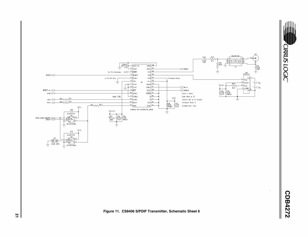
The CS4272 requires careful attention to power supply and grounding arrangements to opti-mize performance. Figure 5 provides an overview of the connections to the CS4272,Figure 16 shows the component placement, Figure 17 shows the top layout, and Figure 18shows the bottom layout. The decoupling capacitors are located as close to the CS4272 aspossible. Extensive use of ground plane fill in the evaluation board yields large reductions inradiated noise.
8

CDB4272
CONNECTOR INPUT/OUTPUT SIGNAL PRESENT
+5V - J1 Input +5.0 V Power Supply
-18V - J7 Input -18.0 V to -5.0 V Power Supply for the op-amps
+18V - J6 Input +5.0 V to +18.0 V Power Supply for the op-amps
VA - J5 Input +5.0 V Power Supply for VA
VD - J3 Input +3.3 V to +5.0 V Variable Power Supply for VD
VL - J2 Input +3.3 V to +5.0 V Variable Power Supply for VL
GND - J4 Input Ground Reference
RX-COAX - J25 Input Digital audio input via coaxial cable
RX-OPT - OPT1 Input Digital audio input via optical cable
TX-COAX - J12 Output CS8406 digital audio output via coaxial cable
TX-OPT - J18 Output CS8406 digital audio output via optical cable
PC Port - J31 Input/Output Parallel connection to PC for SPI / I2C control port signals and sys-tem configuration
PCM HEADER - J26 Input/Output I/O for Clocks & Data
8416 SDOUT - J24 Output CS8416 serial data output (SDOUT)
8406 SDIN - J17 Input External data source for CS8406 SDIN
EXT CTRL I/O Input/Output I/O for external SPI / I2C control port signals (J32) and control signalheader in/out selection (J34)
AINL - J33AINR - J30
Input XLR jacks for differential analog input signal to CS4272
AOUTL - J23AOUTR - J16
Output RCA phono jacks for analog outputs
Table 1. System Connections
9

CDB4272
JUMPER /SWITCH PURPOSE POSITION FUNCTION SELECTED
M/S[1:0](S1)
Subclock Master/Slave Select *00011011
CS4272 is MasterCS8416 is MasterCS8406 is MasterPCM Header, J26, is Master
MCLK[1:0](S1)
Master Clock Source Select *00011011
CS8416 Provides MCLKCS4272 Provides MCLKPCM Header, J26, Provides MCLKPCM Header, J26, Provides MCLK
Header/8416(S1)
CS4272 SDIN Source Select *01
CS8416 Provides SDIINPCM Header, J26, Provides SDIN
Coaxial/Optical
(S1)
Optical or Coaxial S/PDIFInput Select
*01
Optical InputCoaxial Input
I2S/LJ(S1)
Digital Interface Format Select *01
Left Justified, 24-bitI2S, 24-Bit
128/256(S1)
Master Clock Speed Select *01
256*Fs128*Fs
M[1:0](S1)
CS4272 Speed Mode Select 00*011011
Single-Speed Mode, with De-emphasisSingle-Speed Mode, w/out De-emphasisDouble-Speed ModeQuad-Speed Mode
J11, J19 Selects LED or Mute Circuit forAOUTA, AOUTB
1*2
Mute Circuit Affects Analog OutputMute Circuit Disconnected (LED displaysxMUTEC status)
J10 Selects source of voltage forthe VA supply
*+5VADJ
Voltage source is J1, +5.0 V binding postVoltage source is J5, VA binding post
J9 Selects source of voltage forthe VD supply
*+5V+3.3VADJ
Voltage source is J1, +5V binding postVoltage source is +3.3 V regulatorVoltage source is J3, VD binding post
J8 Selects source of voltage forthe VL supplies
*+5V+3.3VADJ
Voltage source is J1, +5V binding postVoltage source is +3.3 V regulatorVoltage source is J2, VL binding post
J13, J14,J15, J20,J21, J22
Selects DAC Output Filter *12
Selects standard 2-pole filterInserts instrumentation-amp and resistordivider.
*Default factory settings
Table 2. Jumper/Switch Settings
10

CDB4272
2. INITIAL BOARD SETUP
2.1 Power Supplies:
1) Verify that all power supplies are off before making connections.
2) Connect a +5.0 VDC power supply to the +5V (J1) red binding post. If correct configura-tion is other than the factory default, select VL and VD operating voltage by placing ajumper on J8 and J9 to select either +5.0 V or +3.3 V.
3) Connect a +18.0 to +5.0 VDC power supply to the +18V (J6) green binding post. If usingthe FILT position number 2 for the output filter stage, +18.0 V is required on J6.
4) Connect a -18.0 to -5.0 VDC power supply to the -18V (J7) yellow binding post. If usingthe FILT position number 2 for the output filter stage, -18.0 V is required on J7.
5) Connect the common ground of the power supplies to the GND (J4) binding post.
6) Attach all required analog and digital cables to the board jacks and connectors.
7) If software control is desired, attach parallel port cable between board and PC.
8) If using the External Control Header connection, attach the required user supplied flat rib-bon cable to the header with the power supplies turned off.
9) With all cables and connections in place, turn on the power supplies to the board. Turn onsupplies in this order: +5 V, +18 V, -18 V.
10)Press and release the RESET switch S2. The LED, D5, will illuminate as long as S2 isdepressed indicating a reset condition. Once S2 is released, the LED should turn off. If itremains on, an error has occurred. At this point, power off the power supplies and re-check all connections. Apply power to the board and press and release S2. Once the LEDhas turned off, the board will be setup for use.
2.2 Installing the Software:
1) Create a directory called CDB4272 anywhere on your PC.
2) Copy CDB427X.exe from the included CD into this directory.
3) Run port95nt.exe from the CD. After running the program the system will need tobe restarted.
4) If desired, create a shortcut to CDB427X.exe on your desktop. You should now be able torun CDB427X.exe. Double-click on CDB427X.exe or its shortcut.
5) Select the LPT port you are using to connect to the CDB4272.
6) Shut down the application, reset the board, and then restart the application.
11

CDB4272
2.2.1Verifying Board Operation:
1) If connected, disconnect the PC parallel cable.
2) Set all positions on S1 to LO, with the exception of M0 which should be set to HI.
3) Assert a reset by pressing the RESET button (S2).
4) Apply a S/PDIF input signal to the optical connector (OPT1). The converted signal shouldappear at the analog output jacks AOUTR and AOUTL.
5) Apply an analog input signal to the analog input jacks AINR and AINL. The converted sig-nal should appear at the S/PDIF TX output jacks (J12 and J18).
12

CDB4272
3. CDB427X.EXE USER'S GUIDE
3.1 Main Window
The main window of the CDB4272 Graphical User Interface allows the user to view andchange the configuration of the CS4272 and on-board configuration logic.
The Board Setup box contains all the controls necessary to manage clock and data routingand formats. To apply changes to the board, the “Send Board Setup” button must be pressedafter making changes within the Board Setup box.
The CS4271/2 Setup box allows configuration of the internal registers of the CS4272. Chang-es made within this box will be reflected immediately. When in I2C mode, the “Update” buttonwill read the registers of the CS4272 and update the CS4271/2 Setup box to match.
Clicking the “Advanced...” button will launch a graphical register map of the CS4272.
Figure 2. Main Window
13

CDB4272
3.2 Advanced Window
Clicking the “Advanced...” button on the main window will launch a graphical register map ofthe CS4272. Changes made to the register map will be immediately reflected in the main win-dow, so you may wish to arrange them so that they do not obscure each other. When in I2Cmode, the “Update” button will read the registers of the CS4272 and update the AdvancedRegister Settings box to match. See Figure 3 below.
3.3 I2C Mode No Acknowledge Error
The control port of the CS4272 requires the presence of an MCLK signal for correct opera-tion. Because of this, if the board is set up to receive MCLK from a source that isn’t activelyproviding the signal, a no acknowledge error may result. This means that the GUI is expectingan acknowledgement from the CS4272, but isn’t receiving it. If this occurs, ensure that theappropriate source of MCLK is providing the signal. For example, if the board is set up to re-ceive MCLK from the header, be sure that there is an active MCLK signal applied to theMCLK position on the header (J26). See Figure 4 below.
Figure 3. Advanced Window
Figure 4. I2C Error Message
14

CD
B427215
4.B
LO
CK
DIA
GR
AM
CS8406
OMCK
ISCLKILRCK
ource
SDIN
CS8416
MC
LK
LRC
K
SC
LK
RMCK
OSCLK
OLRCK
MCLK I/OLRCK I/OSCLK I/O
SDIN InSDOUT Out
RMCKDisable
Subclock DirMCLK Dir
C annedO scilla tor
OMCK
SDOUT
SDIN
4272 SDIN Source
8416 SDOUT
8406 SDIN S
8406 SDIN
SDOUT
(HW/SW)
(HW/SW)
(HW/SW)
(HW/SW)
(SW)
XT
I
XT
O
CS4272
Figure 5. Clock and Data Routing

CD
B4272
16 5.S
CH
EM
AT
ICS
AN
DL
AY
OU
T
Figure 6. Hierarchy, Schematic Sheet 1

CD
B427217
Figure 7. CS4272, Schematic Sheet 2

CD
B4272
18
Figure 8. AnalogI nput, Schematic Sheet 3

CD
B427219
Figure 9. Analog Output, Schematic Sheet 4

CD
B4272
20
Figure 10. CS8416 S/PDIF Receiver, Schematic Sheet 5
CD
B427221
Figure 11. CS8406 S/PDIF Transmitter, Schematic Sheet 6

CD
B4272
22
Figure 12. Board Setup, Schematic Sheet 7

CD
B427223
Figure 13. PCM Header, Schematic Sheet 8

CD
B4272
24
Figure 14. Control Port, Schematic Sheet 9

CD
B427225
Figure 15. Power, Schematic Sheet 10

CD
B4272
26
Figure 16. Component Placement and Reference Designators

CD
B427227
Figure 17. Top Layer
CD
B4272
28
Figure 18. Bottom Layer

CDB4272
6. APPENDIX
6.1 Board Modifications
There are two modifications to the circuit board as follows:
1) Locations R9 and R47 are each populated with 6 parallel 1/8 W 7.87 kΩ resistors to pro-vide a combined resistance of 1.312 kΩ and a combined power dissipation rating of3/4 W.
Locations R22 and R60 are each populated with 2 parallel 1/8 W 681 Ω resistors to provide acombined resistance of 341 Ω and a combined power dissipation rating of 1/4 W.
29

CD
B4272
30
6.2C
om
plete
An
alog
Inp
ut
Bu
fferS
chem
atic
Figure 19. Complete Analog Input Buffer Schematic

• Notes •