Embed Size (px)
Citation preview

DALSA Corporation 2009
CCD Image Sensors for Astronomy
Erik Bogaart, Inge Peters, Jan Bosiers, and Nixon O
DALSA Professional ImagingEindhoven, The Netherlands
October 13th, 2009
& CMOS

2DALSA Corporation 2009 - Bogaart
Outline
• DALSA Corp.
• CCD Image Sensors• Architecture• Ultra-low dark current• Backside thinned devices
• CMOS Image Sensors• Wafer-scale• Radiation hardness
• Summary

3DALSA Corporation 2009 - Bogaart
DALSA Corp at a Glance
• Established in 1980• Headquarters in Waterloo ON, Canada• Listed at Toronto Stock Exchange
• Stock Symbol: DSA (TSX)• Shares Outstanding: ~20M
4DALSA Corporation 2009 - Bogaart
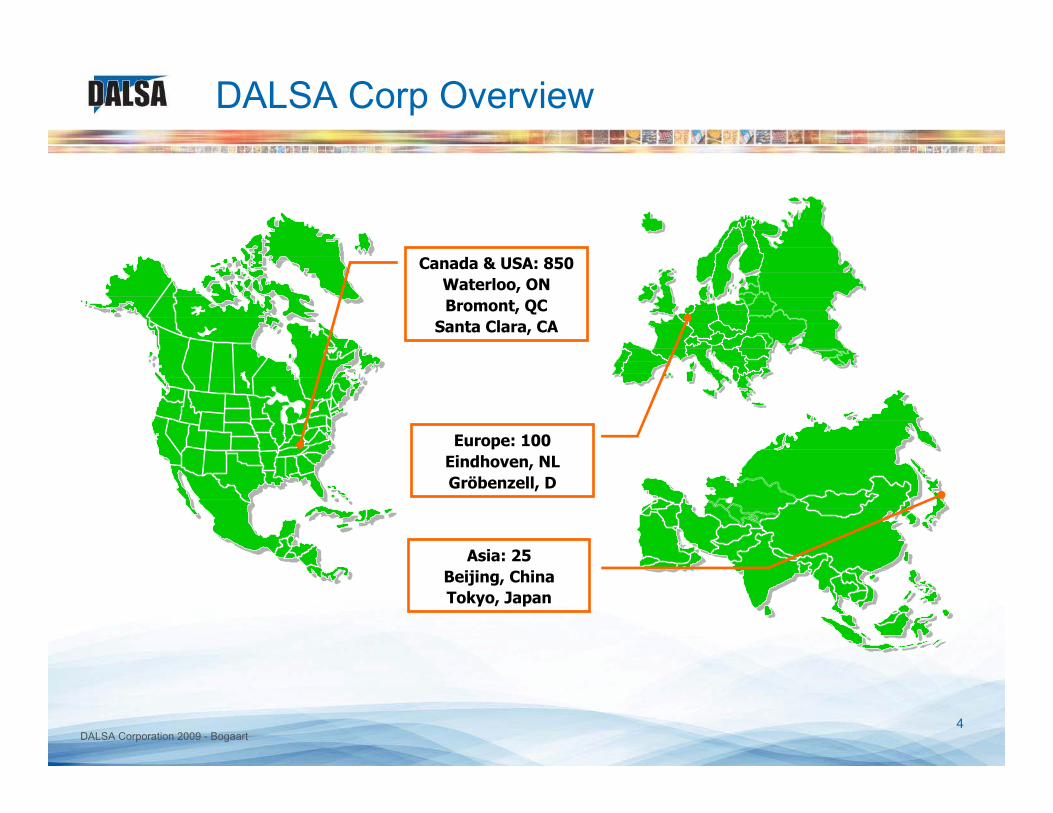
DALSA Corp Overview
Europe: 100Eindhoven, NLGröbenzell, D
Asia: 25Beijing, ChinaTokyo, Japan
Canada & USA: 850Waterloo, ONBromont, QC
Santa Clara, CA

5DALSA Corporation 2009 - Bogaart
DALSA Corp – Our Businesses
• Semiconductor fab - Bromont, Canada• CCD & CMOS image sensors• Digital cameras• Vision processors & software
Image sensors
MEM technology

6DALSA Corporation 2009 - Bogaart
DALSA Corp – Our Businesses
• Semicondcutor fab - Bromont, Canada• CCD & CMOS image sensors• Digital cameras• Vision processors & software
Professional DSC
Broadcast& video

7DALSA Corporation 2009 - Bogaart
DALSA Corp – Our Businesses
• Semiconductor fab - Bromont• CCD & CMOS image sensors• Digital cameras• Vision processors & software Medical X-ray &
Dental applications

8DALSA Corporation 2009 - Bogaart
DALSA Corp – Our Businesses
• Semiconductor fab - Bromont• CCD & CMOS image sensors• Digital cameras• Vision processors & software
AerialPhotogrammetry
Scientific& Space

9DALSA Corporation 2009 - Bogaart
DALSA Corp – Our Businesses
• Semiconductor fab - Bromont, Canada• CCD & CMOS image sensors• Digital cameras• Vision processors & software

10DALSA Corporation 2009 - Bogaart
Outline
• DALSA Corp.
• CCD Image Sensors• Architecture• Ultra-low dark current• Backside thinned devices
• CMOS Image Sensors• Wafer-scale• Radiation hardness
• Summary
11DALSA Corporation 2009 - Bogaart
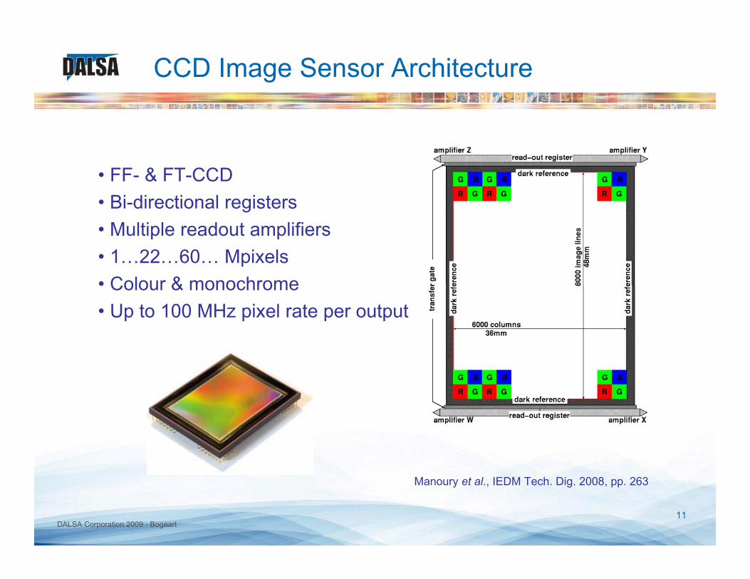
CCD Image Sensor Architecture
• FF- & FT-CCD• Bi-directional registers• Multiple readout amplifiers• 1…22…60… Mpixels• Colour & monochrome• Up to 100 MHz pixel rate per output
Manoury et al., IEDM Tech. Dig. 2008, pp. 263
12DALSA Corporation 2009 - Bogaart
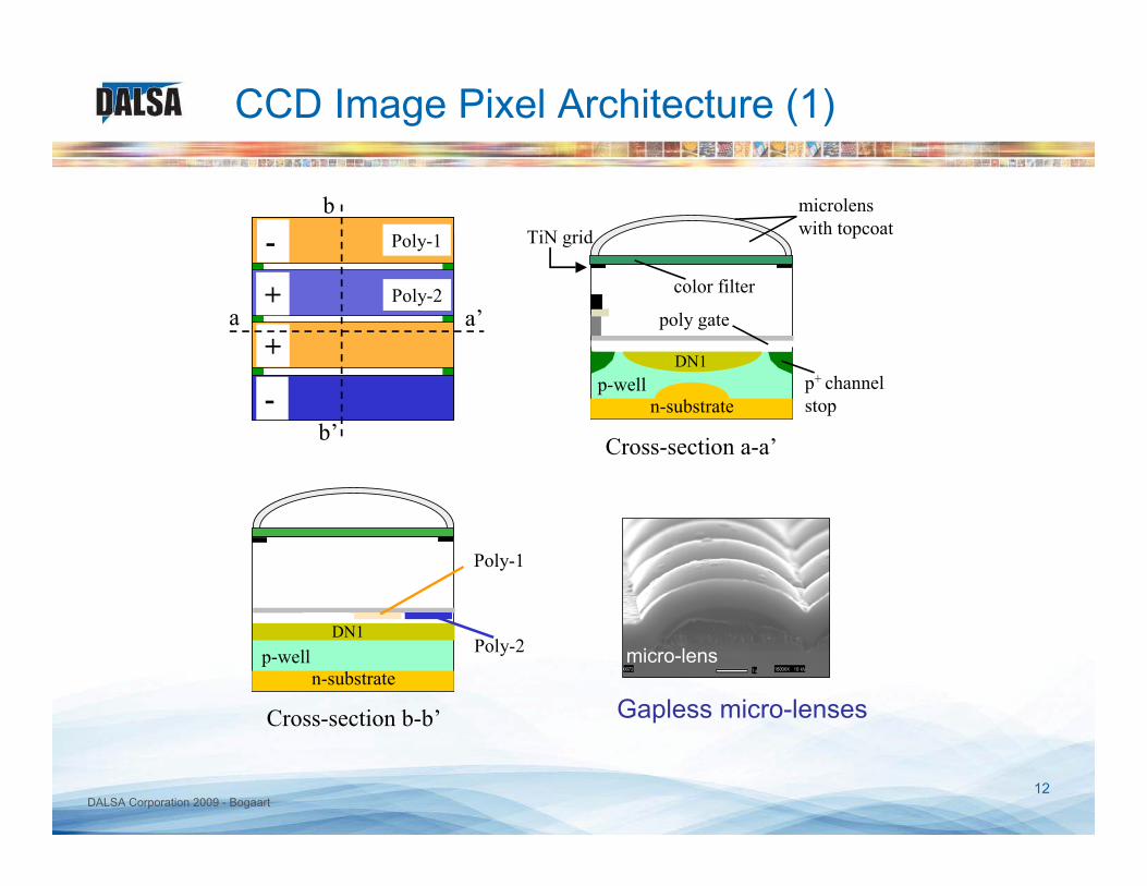
Poly-1
Poly-2+
+
-
-
color filter
TiN grid
p-well p+ channelstop
a a’
microlenswith topcoat
DN1
n-substrate
poly gate
n-substrate
DN1p-well
b
b’ Cross-section a-a’
Cross-section b-b’
Poly-1
Poly-2
CCD Image Pixel Architecture (1)
micro-lens
Gapless micro-lenses
13DALSA Corporation 2009 - Bogaart
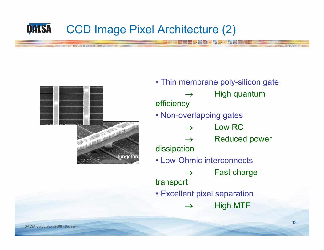
CCD Image Pixel Architecture (2)
tungsten
• Thin membrane poly-silicon gate→ High quantum
efficiency• Non-overlapping gates
→ Low RC→ Reduced power
dissipation• Low-Ohmic interconnects
→ Fast charge transport• Excellent pixel separation
→ High MTF

14DALSA Corporation 2009 - Bogaart
CCD Image Pixel Architecture (3)
nitride layer
microlenswith topcoat
n-channel
n-substratep-well
p+ channelstop
poly gate
TiN grid
14
12
10
8
6
n-substratep-welln-channelP
oten
tial (
V)Depth in silicon
0.0
1.0
2.0
3.0
4.0
SiO
2
Silicon
e-density under the integrating gate
integrating gate
blocking gate
barrier to neighboranti-blooming barrier
Ele
ctro
n de
nsity
(arb
. uni
ts)
• 4-phase buried-channel
• Vertical overflow drain to handle overexposure
• Low dark current
• High charge capacity
• Fast electronic shuttering Bogaart et al., Proc. SPIE 7250, pp. 725 003 (2009)
15DALSA Corporation 2009 - Bogaart
Outline
• DALSA Corp.
• CCD Image Sensors• Architecture• Ultra-low dark current• Backside thinned devices
• CMOS Image Sensors• Wafer-scale• Radiation hardness
• Summary

16DALSA Corporation 2009 - Bogaart
Dark Current in Image Pixels
Dark current generation can be divided in three components:
Suppression• ISurface: interface of the buried channel biased into inversion
→ MPP• IBulk: built-in potential barrier reduces carrier diffusion
→ vertical anti-blooming
++=
++=
nA
ni
ggi
BulkDepletionSurfaceDark
LNDnWSqn
IIII
τ
Bogaart et al., IEEE TED (2009) accepted

17DALSA Corporation 2009 - Bogaart
CCD image sensors - Ultra-low dark current (1)
Multi-pinned phase
Anti-blooming
Electronic shuttering
All-gates pinning(AGP)
Poly-1
Poly-2+
+
-
-
color filter
TiN grid
p-well p+ channelstop
a a’
DN1
n-substrate
-
-
-
-
a a’
n-substrate
tungsten wirepoly gate
DN1 + DN2
Additional n-channelimplant area
n-substrate
DN1p-well
n-substratep-well
DN1DN1+DN2
b
b’
Cross-section a-a’
Cross-section b-b’
contact
p-well
Standard AGP
Bosiers et al., IEEE TED 42, 1449 (1995)Peters et al., IEDM Tech. Dig. 2004, pp. 993

18DALSA Corporation 2009 - Bogaart
CCD Image Sensors – Ultra-low dark current (2)
0 50 100 150 200
1
10
100
1000
10000
# o
f pix
els
Signal level (DN)0 50 100 150 200
1
10
100
1000
10000
# of
pix
els
Signal level (DN)
Non-AGP AGP
Dark images at room temperature with 6 s integration time(equally contrast enhanced)

19DALSA Corporation 2009 - Bogaart
CCD Image Sensors – Ultra-low dark current (3)
80x reductionDark current over full well factor (DCFF) improved 28x
80 fA/cm2 @ 10 °C
Allows low-light imaging, long integration times, and astronomical observations at elevated temperatures
Bogaart et al., IEEE TED (2009) accepted
3.0 3.2 3.4 3.6
0.1
1
10
100
AGP pixel
non-AGP pixel
I Dar
k (pA
/cm
2 )
1000/T (K-1)
20DALSA Corporation 2009 - Bogaart
Outline
• DALSA Corp.
• CCD Image Sensors• Architecture• Ultra-low dark current• Backside thinned devices
• CMOS Image Sensors• Wafer-scale• Radiation hardness
• Summary

21DALSA Corporation 2009 - Bogaart
CCD Image Sensors - Backside thinned devices (1)
• Backside thinning: p--epi on p+ andSOI substrates
• Die thinning up to 10 × 10 cm2 devices• Wafer level thinning on 6″ wafers• Si-thickness ~ 8..12 µm• In-bumps, OK at cryogenic temperatures
Substrate
CCD~ 12 µm
Au
In

22DALSA Corporation 2009 - Bogaart
CCD Image Sensors - Backside thinned devices (2)
200 400 600 800 10000
20
40
60
80
100
16 µm pixel, ~ 10 µm Si-thickness
15 nm HfO2
20 nm HfO2
VIS-NIR
Optimized for UV
New resultsM
easu
red
QE
(%)
Wavelength (nm)

23DALSA Corporation 2009 - Bogaart
Outline
• DALSA Corp.
• CCD Image Sensors• Architecture• UItra-low dark current• Backside thinned devices
• CMOS Image Sensors• Wafer-scale• Radiation hardness
• Summary

24DALSA Corporation 2009 - Bogaart
CMOS Image Sensors – Wafer-scale (1)
• 8” wafer, p-substrate
• 77 x 145 mm2 active area
• 33.55 µm pixel pitch
• 2,304 x 4,320 resolution
• Buttable on three sides
• Radiation-hard pixel design

25DALSA Corporation 2009 - Bogaart
CMOS Image Sensors – Wafer-scale (2)
• 2 x 3 CMOS sensors tiled toCsI-coated FOP
• 231 x 290 mm2 active area
• 6,912 x 8,640 resolution(60 Mpixel)
26DALSA Corporation 2009 - Bogaart
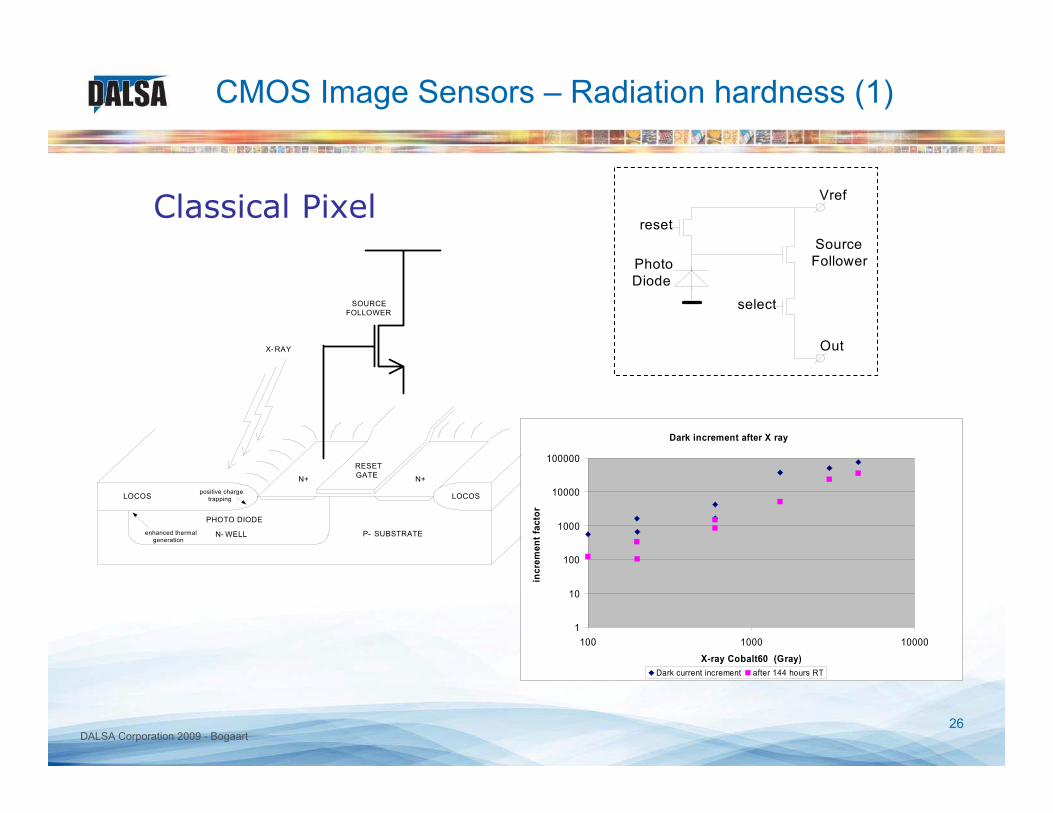
CMOS Image Sensors – Radiation hardness (1)
PHOTO DIODE
N- WELL P- SUBSTRATE
LOCOS
N+ N+
RESETGATE
positive chargetrappingLOCOS
enhanced thermal generation
SOURCE FOLLOWER
X- RAY
Dark increment after X ray
1
10
100
1000
10000
100000
100 1000 10000X-ray Cobalt60 (Gray)
incr
emen
t fac
tor
Dark current increment after 144 hours RT
Vref
Out
reset
select
SourceFollowerPhoto
Diode
Classical Pixel

27DALSA Corporation 2009 - Bogaart
CMOS Image Sensors – Radiation hardness (2)
Radiation Hard PPD Pixel
100x better radiation hard
0 25 50 75 1000
2
4
6
8
10Cobalt 60 - 1.2 MeV
Dar
k cu
rren
t inc
reas
e fa
ctor
Radiation dose (Gray)
Measurement Linear fit
28DALSA Corporation 2009 - Bogaart
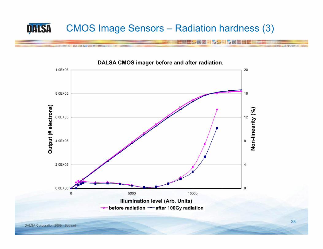
CMOS Image Sensors – Radiation hardness (3)
DALSA CMOS imager before and after radiation.
0.0E+00
2.0E+05
4.0E+05
6.0E+05
8.0E+05
1.0E+06
0 5000 10000
Illumination level (Arb. Units)
Out
put (
# el
ectr
ons)
0
4
8
12
16
20
Non
-line
arity
(%)
before radiation after 100Gy radiation

29DALSA Corporation 2009 - Bogaart
• World record ultra-low dark current CCD image sensor with All-Gates Pinning» 1.5 pA/cm2 @ 60 °C» 0.08 pA/cm2 @ 10 °C
• Dark current over full well factor (DCFF) improved 28x(6 µm pixel)
• Charge transport efficiency, anti-blooming, and electronic shuttering performance are not compromised
• Die level – 10x10 cm2 – and 6” wafer level BST CCD» UV – QE 94% @ 240 nm» VIS – QE 97% @ 565 nm
• 8” Wafer scale buttable CMOS image sensor• PPD pixel design, radiation hardness 100x better
Summary

30DALSA Corporation 2009 - Bogaart
Thank youfor your attention
Info: www.dalsa.com/sensors/E-mail: [email protected]