Embed Size (px)
Citation preview

CATALOG
Fixed Resistors
2018
2018.3 industrial.panasonic.com/

– 1 –
Fixed Resistors CONTENTS
All products in this catalog comply with the RoHS Directive.
The RoHS Directive is “the Directive (2011/65/EU) on the Restriction of the Use of Certain
Hazardous Substances in Electrical and Electronic Equipment “ and its revisions.
Classifi cation Product Item Part No. Page
Safety Precautions (Common precautions for Fixed Resistors) 2
Surface MountResistors
Chip Resistors
Thick Film Chip Resistors ERJ XG, 1G, 2G, 3G, 6G, 8G, 14, 12, 12Z, 1T 3
Precision Thick Film Chip Resistors ERJ XG, 1G, 1R, 2R, 3R, 6R, 3E, 6E, 8E, 14, 12, 1T 6
High Precision
Metal Film (Thin Film) Chip Resistors,
High Reliability TypeERA 1A, 2A, 3A, 6A, 8A 10
Current Sensing
Thick Film Chip Resistors
/ Low Resistance Type
ERJ 2LW, 3LW, 6LW, 2BW,3BW,6BW,8BW,6CW,8CW
ERJ 2B, 3B, 6D, 6B, 8B, 14B, 3R, 6R, 8R, 14R, 12R,12Z,
ERJ 1TR, L03, L06, L08, L14, L12, L1D, L1W
13
Current Sensing Resistors, Metal Plate Type ERJ MS4S, MS4H, MS6S, MB1S 18
Current Sensing Resistors, Metal Plate Type ERJ M1WS, M1WT 22
Current Sensing Resistors, Metal Foil Type ERJ MFBA 24
High Power Chip Resistors / Wide Terminal Type ERJ A1, B1, B2, B3 26
Small&High Power
High Precision
Thick Film Chip ResistorsERJ PB3, PB6 30
Anti-Surge Thick Film Chip Resistors ERJ PA2, P03, PA3, P06, P08, P14 32
Anti-Pulse Thick Film Chip Resistors ERJ T06, T08, T14 35
Anti-Sulfurated
Anti-Sulfurated Thick Film
Chip Resistors
ERJ S02, S03, S06, S08, S14, S12, S1D, S1T
ERJ U01, U02, U03, U06, U08, U14, U12, U1D, U1T
ERJ U6S, U6Q
38
Anti-Sulfurated Thick Film Chip Resistors /
Anti-Surge TypeERJ UP6, UP8 41
Anti-Sulfurated High Power Chip Resistors /
Wide Terminal TypeERJ C1 44
Resistor Network/Array
Chip Resistor ArrayEXB 14V, 18V, 24V, 28V, N8V, 2HV, 34V,
V4V, 38V, V8V, S8V46
Anti-Sulfurated Chip Resistor Array EXB U14, U18, U24, U28, U2H, U34, U38 50
Chip Resistor Networks EXB D, E, A, Q 53
Chip Attenuator EXB 14AT, 24AT 55
Commonspecifi cations
Packaging Methods (Taping) 57
Recommended Land Pattern 62
Recommended Soldering Conditions 64
Safety Precautions (Common precautions for Surface Mount Resistors) 65
PowerType Resistors
(Leaded)
Metal (Oxide) Film Resistors,
Flame-Retardant
ERG 12S, 1S, 1F, 2S, 2F, 3S, 3F, 5S, 5F
ERX 12S, 1S, 1F, 2S, 2F, 3S, 3F, 5S, 5F66
Anti-Pulse Power Resistors ERG 12D, 1D, 2D, 3D 73
Metal Film Resistors / Low Resistance Value ERX 12L, 1L, 2L 75
Fusing Resistors Metal Film Fusing ResistorsERQ 1Z, 2Z, 12Z, 14Z
ERQ 1AB, 2AB, 12A, 14A77
Fixed Resistors Appendix 83
Mar. 201804
– 2 –
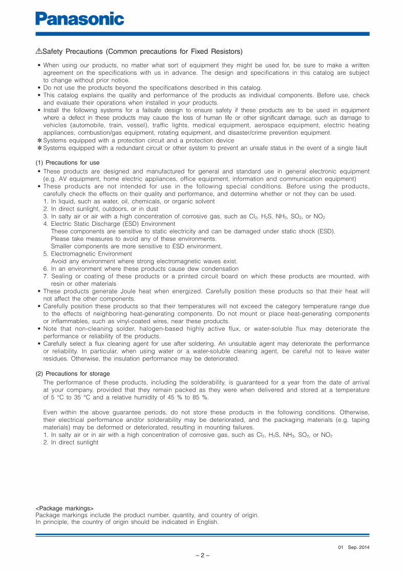
Safety Precautions (Common precautions for Fixed Resistors)
• When using our products, no matter what sort of equipment they might be used for, be sure to make a written
agreement on the specifications with us in advance. The design and specifications in this catalog are subject
to change without prior notice.
• Do not use the products beyond the specifications described in this catalog.
• This catalog explains the quality and performance of the products as individual components. Before use, check
and evaluate their operations when installed in your products.
• Install the following systems for a failsafe design to ensure safety if these products are to be used in equip ment
where a defect in these products may cause the loss of human life or other significant dam age, such as damage to
vehicles (automobile, train, vessel), traffic lights, medical equipment, aerospace equipment, electric heating
appliances, combustion/gas equipment, rotating equipment, and disaster/crime prevention equipment.
✽ Systems equipped with a protection circuit and a protection device
✽ Systems equipped with a redundant circuit or other system to prevent an unsafe status in the event of a sin gle fault
(1) Precautions for use
• These products are designed and manufactured for general and standard use in general elec tron ic equipment
(e.g. AV equipment, home electric appliances, office equipment, information and communication equipment)
• These products are not intended for use in the following special conditions. Before using the products,
carefully check the effects on their quality and performance, and determine whether or not they can be used.
1. In liquid, such as water, oil, chemicals, or organic solvent
2. In direct sunlight, outdoors, or in dust
3. In salty air or air with a high concentration of corrosive gas, such as Cl2, H2S, NH3, SO2, or NO2
4. Electric Static Discharge (ESD) Environment
These components are sensitive to static electricity and can be damaged under static shock (ESD).
Please take measures to avoid any of these environments.
Smaller components are more sensitive to ESD environment.
5. Electromagnetic Environment
Avoid any environment where strong electromagnetic waves exist.
6. In an environment where these products cause dew condensation
7. Sealing or coating of these products or a printed circuit board on which these products are mounted, with
resin or other materials
• These products generate Joule heat when energized. Carefully position these products so that their heat will
not affect the other components.
• Carefully position these products so that their temperatures will not exceed the category temperature range due
to the effects of neighboring heat-generating components. Do not mount or place heat-generating components
or inflammables, such as vinyl-coated wires, near these products.
• Note that non-cleaning solder, halogen-based highly active flux, or water-soluble flux may deteriorate the
performance or reliability of the products.
• Carefully select a flux cleaning agent for use after soldering. An unsuitable agent may deteriorate the performance
or reliability. In particular, when using water or a water-soluble cleaning agent, be careful not to leave water
residues. Otherwise, the insulation performance may be deteriorated.
(2) Precautions for storage
The performance of these products, including the solderability, is guaranteed for a year from the date of ar riv al
at your company, provided that they remain packed as they were when delivered and stored at a tem per a ture
of 5 °C to 35 °C and a relative humidity of 45 % to 85 %.
Even within the above guarantee periods, do not store these products in the following conditions. Otherwise,
their electrical performance and/or solderability may be deteriorated, and the packaging materials (e.g. taping
materials) may be deformed or deteriorated, resulting in mounting failures.
1. In salty air or in air with a high concentration of corrosive gas, such as Cl2, H2S, NH3, SO2, or NO2
2. In direct sunlight
<Package markings>Package markings include the product number, quantity, and country of origin.In principle, the country of origin should be indicated in English.
Sep. 201401
Design and specifications are each subject to change without notice. Ask factory for the current technical specifications before purchase and/or use.
Should a safety concern arise regarding this product, please be sure to contact us immediately.
Thick Film Chip Resistors
– 3 –
E
1
R
2
J
3
3
4
G
5
E
6
Y
7
J
8
1
9
0
10
2
11
V
12
Thick FilmChip Resistors
Product Code Size, Power Rating
01005
0201
0402
0603
0805
1206
1210
1812
2010
2512
XGN
1GN
2GE
3GE
6GE
8GE
14
12
12Z
1T
0.031 W
0.05 W
0.1 W
0.1 W
0.125 W
0.25 W
0.5 W
0.75 W
0.75 W
1 W
Power R.
Marking
Code
Y
✽Nil
Marking
Value Marking onblack side
No marking
Resistance Tolerance
Code
J
0
Tolerance
±5 %
Jumper
The first two digits are significant figures of resistance and the third one denotes number of zeros following. Decimal Point is expressed by R as 4.7 = 4R7.
Jumper is expressed by R00.
Resistance Value
Packaging Methods
Code
Y
U
Packaging Part No.
Embossed Carrier Taping W4P1, 40,000 pcs.
Pressed Carrier Taping W8P2, 20,000 pcs.
CPressed Carrier Taping 2 mm pitch, 15,000 pcs.
ERJXGN
X
YPunched Carrier Taping 2 mm pitch, 20,000 pcs.
U
Embossed Carrier Taping 4 mm pitch, 5,000 pcs.
Punched Carrier Taping 2 mm pitch, 10,000 pcs.
ERJ2GE
ERJ1GN
Embossed Carrier Taping 4 mm pitch, 4,000 pcs. ERJ1T
ERJ14
ERJ12
ERJ12Z
Code
VPunched Carrier Taping 4 mm pitch, 5,000 pcs.
ERJ3GE
ERJ6GE
ERJ8GE
Inch
Thick Film Chip Resistors
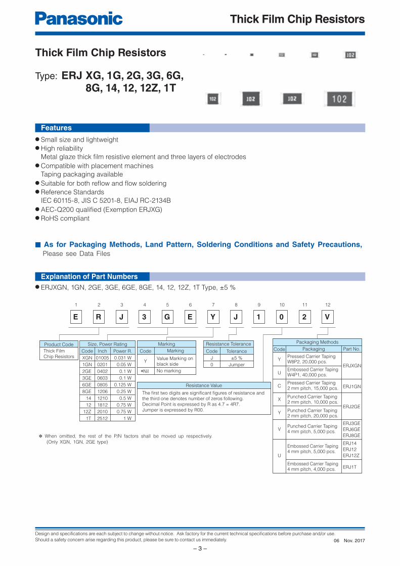
Type: ERJ XG, 1G, 2G, 3G, 6G, 8G, 14, 12, 12Z, 1T
Explanation of Part Numbers
Features
● Small size and lightweight● High reliability
Metal glaze thick fi lm resistive element and three layers of electrodes
● Compatible with placement machines
Taping packaging available
● Suitable for both refl ow and fl ow sol der ing● Reference Standards
IEC 60115-8, JIS C 5201-8, EIAJ RC-2134B
● AEC-Q200 qualifi ed (Exemption ERJXG)● RoHS compliant
✽ When omitted, the rest of the P/N factors shall be moved up respectively.
(Only XGN, 1GN, 2GE type)
■ As for Packaging Methods, Land Pattern, Soldering Conditions and Safety Precautions, Please see Data Files
● ERJXGN, 1GN, 2GE, 3GE, 6GE, 8GE, 14, 12, 12Z, 1T Type, ±5 %
Nov. 201706

Design and specifications are each subject to change without notice. Ask factory for the current technical specifications before purchase and/or use.
Should a safety concern arise regarding this product, please be sure to contact us immediately.
Thick Film Chip Resistors
– 4 –
Protective coating
Alumina substrate Electrode (Inner)
Electrode
(Between)
Thick filmresistive element Electrode (Outer)
–40 –20 0 20 40 60 80 100 120 140 1600
180–60
155 °C
70 °C
Ambient Temperature (°C)
20
40
60
80
100
Rate
d L
oad
(%
)
–55 °C
2G, 3G, 6G, 8G,
14, 12, 12Z, 1T
XG, 1G
125 °C
a
b
t
W
L
Ratings
Part No.Dimensions (mm) Mass (Weight)
(g/1000 pcs.)L W a b t
ERJXG 0.40±0.02 0.20±0.02 0.10±0.03 0.10±0.03 0.13±0.02 0.04
ERJ1G 0.60±0.03 0.30±0.03 0.10±0.05 0.15±0.05 0.23±0.03 0.15
ERJ2G 1.00±0.05 0.50±0.05 0.20±0.10 0.25±0.05 0.35±0.05 0.8
ERJ3G 1.60±0.15 0.80+0.15 0.30±0.20 0.30±0.15 0.45±0.10 2
ERJ6G 2.00±0.20 1.25±0.10 0.40±0.20 0.40±0.20 0.60±0.10 4
ERJ8G 3.20+0.05 1.60+0.05 0.50±0.20 0.50±0.20 0.60±0.10 10
ERJ14 3.20±0.20 2.50±0.20 0.50±0.20 0.50±0.20 0.60±0.10 16
ERJ12 4.50±0.20 3.20±0.20 0.50±0.20 0.50±0.20 0.60±0.10 27
ERJ12Z 5.00±0.20 2.50±0.20 0.60±0.20 0.60±0.20 0.60±0.10 27
ERJ1T 6.40±0.20 3.20±0.20 0.65±0.20 0.60±0.20 0.60±0.10 45
–0.05
–0.15–0.20
Part No.
(inch size)
Power Rating (3)
at 70 °C
(W)
Limiting Element
Voltage (1)
(V)
Maximum Overload
Voltage (2)
(V)
Resistance
Tolerance
(%)
Resistance
Range
(Ω)
T.C.R.
(×10–6/°C)
Category
Temperature Range
(°C)
AEC-Q200
Grade
ERJXG(01005) 0.031 15 30 ±5 4.7 to 1M (E24)
<10 Ω : –100 to +60010 Ω to 100 Ω : ±300100 Ω< : ±200
–55 to +125 –
ERJ1G(0201) 0.05 25 50 ±5 1 to 10M (E24)
<10 Ω:–100 to +600
10 Ω to 1M Ω:±200
1M Ω<:–400 to +150
–55 to +125 Grade 1
ERJ2G(0402) 0.1 50 100 ±5 1 to 10M (E24) –55 to +155 Grade 0
ERJ3G(0603) 0.1 75 150 ±5 1 to 10M (E24) –55 to +155 Grade 0
ERJ6G(0805) 0.125 150 200 ±5 1 to 10M (E24) –55 to +155 Grade 0
ERJ8G(1206) 0.25 200 400 ±5 1 to 10M (E24) –55 to +155 Grade 0
ERJ14(1210) 0.5 200 400 ±5 1 to 10M (E24) –55 to +155 Grade 0
ERJ12(1812) 0.75 200 500 ±5 1 to 10M (E24) –55 to +155 Grade 0
ERJ12Z(2010) 0.75 200 500 ±5 1 to 10M (E24) –55 to +155 Grade 0
ERJ1T(2512) 1 200 500 ±5 1 to 1M (E24) –55 to +155 Grade 0
Part No.(inch size)
Rated Current(A)
Maximum Over load Current (1)
(A)
ERJXG (01005)0.5 1
ERJ1G (0201)ERJ2G (0402)
1 2ERJ3G (0603)ERJ6G (0805)
2 4
ERJ8G (1206)ERJ14 (1210)ERJ12 (1812)ERJ12Z (2010)ERJ1T (2512)
Power Derating CurveFor resistors operated in ambient temperatures above 70 °C, power rating shall be derated in accordance with the figure below.
[For Resistor]
[For Jumper]
Construction Dimensions in mm (not to scale)
(1) Rated Continuous Working Voltage (RCWV) shall be de ter mined from RCWV=√Power Rating × Re sis tance Values, or Limiting Element Voltage list ed above, whichever less.
(2) Overload Test Voltage (OTV) shall be determined from OTV=Specified Magnification (refer to performance) × RCWV or Maximum Overload Voltage listed above, whichever less.
(3) Use it on the condition that the case temperature is below the upper category temperature.
(1) Overload test current
Nov. 201706

Design and specifications are each subject to change without notice. Ask factory for the current technical specifications before purchase and/or use.
Should a safety concern arise regarding this product, please be sure to contact us immediately.
Thick Film Chip Resistors
– 5 –
Test ItemPerformance Requirements
Test ConditionsResistor type Jumper type
ResistanceWithin Specifi ed
Tolerance50m Ω or less 20 °C
T. C. R.Within Specifi ed
T. C. R.50m Ω or less +25 °C/+155 °C (ERJXG, ERJ1G : +25 °C/+125 °C)
Overload ±2% 50m Ω or lessRated Voltage × 2.5, 5 s
Jumper type : Max. Overload Current, 5 s
Resistance to Soldering Heat ±1% 50m Ω or less 270 °C, 10 s
Rapid Change of
Temperature±1% 50m Ω or less
–55 °C (30min.) / +155 °C (ERJXG, ERJ1G : +125 °C) (30min.),
100 cycles
High Temperature
Exposure±1% 50m Ω or less +155 °C (ERJXG, ERJ1G : +125 °C) , 1000 h
Damp Heat, Steady State ±1% 50m Ω or less 60 °C, 90% to 95 %RH, 1000 h
Load Life in Humidity ±3% 50m Ω or less60 °C, 90% to 95 %RH, Rated Voltage (Jumper type: Rated Current),
1.5 h ON/0.5 h OFF cycle, 1000 h
Endurance at 70 °C ±3% 50m Ω or less70 °C, Rated Voltage(Jumper type: Rated Current),
1.5 h ON/0.5 h OFF cycle, 1000 h
Perfomance
Nov. 201706

Design and specifications are each subject to change without notice. Ask factory for the current technical specifications before purchase and/or use.
Should a safety concern arise regarding this product, please be sure to contact us immediately.
Precision Thick Film Chip Resistors
– 6 –
E
1
R
2
J
3
3
4
R
5
B
6
D
7
1
8
0
9
0
10
V
11
2
12
Product Code
Thick FilmChip Resistors
Size, Power Rating
Code
1R
2R
3R
6R
Power R.
0.05 W
0.063 W
0.1 W
0.1 W
T.C.R. Marking
T.C.R. Code
H
B
K
E
±50×10–6/˚C (1R, 2R)
±50×10–6/˚C (3R, 6R)
±100×10–6/˚C (2R)
±100×10–6/˚C (3R, 6R)
Resistance Value
Resistance Tolerance
Code
D
Tolerance
±0.5 %
Packaging Methods
Code
C
X
V
Pressed Carrier Taping2 mm pitch, 15,000 pcs.
Punched Carrier Taping2 mm pitch, 10,000 pcs.
Punched Carrier Taping4 mm pitch, 5,000 pcs.
ERJ1R
ERJ2R
ERJ3R
ERJ6R
Packaging Part No.
The first three digits are significant figures of resistance
and the last one denotes number of zeros following. Example: 1002 →10k Ω
Inch
0201
0402
0603
0805
Precision Thick Film Chip Resistors
Type: ERJ XG, 1G ERJ 1R, 2R, 3R, 6R ERJ 3E, 6E, 8E, 14, 12, 1T
Explanation of Part Numbers
Features
● Small size and lightweight● High reliability Metal glaze thick fi lm resistive element and three layers of electrodes● Compatible with placement machines Taping packaging available● Suitable for both refl ow and fl ow soldering● Low Resistance Tolerance ERJXG, 1G, 2R, 3E, 6E, 8E, 14, 12, 1T Type : ±1 % ERJ1R, 2R, 3R, 6R Type : ±0.5 %● Reference Standards IEC 60115-8, JIS C 5201-8, EIAJ RC-2134B● AEC-Q200 qualifi ed (Exemption ERJXG, ERJ1R)● RoHS compliant
■ As for Packaging Methods, Land Pattern, Soldering Conditions and Safety Precautions, Please see Data Files
● ERJ1R, 2R, 3R, 6R Type, ±0.5 %
Nov. 201708

Design and specifications are each subject to change without notice. Ask factory for the current technical specifications before purchase and/or use.
Should a safety concern arise regarding this product, please be sure to contact us immediately.
Precision Thick Film Chip Resistors
– 7 –
a
b
t
W
L
E
1
R
2
J
3
8
4
E
5
N
6
F
7
1
8
0
9
0
10
2
11
V
12
Product Code
Thick Film
Chip Resistors
Size, Power Rating
Code
XGN
1GN
2RC
2RK
3EK
6EN
8EN
14N
12N
12S
1TN
Inch
01005
0201
0402
0402
0603
0805
1206
1210
1812
2010
2512
Power R.
0.031 W
0.05 W
0.1 W
0.1 W
0.1 W
0.125 W
0.25 W
0.5 W
0.75 W
0.75 W
1 W
The first three digits are significant figures
of resistance and the last one denotes
number of zeros following.
Decimal point is expressed by "R".
Example : 1002 → 10k Ω
Resistance Value
Resistance Tolerance
Code
F
Tolerance
±1 %
Packaging Methods
Code
UEmbossed Carrier Taping
W4P1, 40,000 pcs.
ERJXGN
CPressed Carrier Taping
2 mm pitch, 15,000 pcs.ERJ1GN
XPunched Carrier Taping
2 mm pitch, 10,000 pcs.ERJ2RCERJ2RK
Embossed Carrier Taping
4 mm pitch, 4,000 pcs.ERJ1TN
VPunched Carrier Taping
4 mm pitch, 5,000 pcs.
ERJ3EK
ERJ6EN
ERJ8EN
U
Embossed Carrier Taping
4 mm pitch, 5,000 pcs.
ERJ14N
ERJ12N
ERJ12S
Packaging Part No.
YPressed Carrier Taping
W8P2, 20,000 pcs.
Construction Dimensions in mm (not to scale)
Protective coating
Alumina substrateElectrode (Inner)
Electrode(Between)
Thick filmresistive element Electrode (Outer)
Part No.Dimensions (mm) Mass (Weight)
[g/1000 pcs.]L W a b t
ERJXG 0.40±0.02
0.20±0.02
0.10±0.03
0.10±0.03
0.13±0.02
0.04
ERJ1G, 1R 0.60±0.03
0.30±0.03
0.10±0.05
0.15±0.05
0.23±0.03
0.15
ERJ2R□ 1.00±0.05
0.50±0.05
0.20±0.10
0.25±0.05
0.35±0.05
0.8
ERJ3R□ERJ3EK 1.60
±0.150.80
+0.150.30
±0.200.30
±0.150.45
±0.102
ERJ6R□ERJ6EN 2.00
±0.201.25
±0.100.40
±0.200.40
±0.200.60
±0.104
ERJ8EN 3.20+0.05
1.60+0.05
0.50±0.20
0.50±0.20
0.60±0.10
10
ERJ14N 3.20±0.20
2.50±0.20
0.50±0.20
0.50±0.20
0.60±0.10
16
ERJ12N 4.50±0.20
3.20±0.20
0.50±0.20
0.50±0.20
0.60±0.10
27
ERJ12S 5.00±0.20
2.50±0.20
0.60±0.20
0.60±0.20
0.60±0.10
27
ERJ1TN 6.40±0.20
3.20±0.20
0.65±0.20
0.60±0.20
0.60±0.10
45
–0.05
–0.15–0.20
● ERJXGN, 1GN, 2RC, 2RK, 3EK, 6EN, 8EN, 14N, 12N, 12S, 1TN Type, ±1%
Nov. 201708

Design and specifications are each subject to change without notice. Ask factory for the current technical specifications before purchase and/or use.
Should a safety concern arise regarding this product, please be sure to contact us immediately.
Precision Thick Film Chip Resistors
– 8 –
–40 –20 0 20 40 60 80 100 120 140 1600
180–60
70 °C–55 °C
Ambient Temperature (°C)
20
40
60
80
100
Rate
d L
oad
(%
)
125 °C 155 °C
2R, 3R, 6R, 3E, 6E, 8E, 14, 12, 1T
XG, 1G, 1R
Part No.(inch size)
Power Ratingat 70 °C (4)
(W)
Limiting Element Voltage (1)
(V)
Maximum Overload Voltage (2)
(V)
ResistanceTolerance
(%)
ResistanceRange
(Ω)
T.C.R.(×10–6/°C)
CategoryTemperature Range
(°C)
AEC-Q200Grade
ERJ1RH(0201)
0.05 15 30 ±0.5 1k to 1M(E24, E96) ±50 –55 to +125 –
ERJ2RH(0402)
0.063 50 100 ±0.5 100 to 100k(E24, E96) ±50 –55 to +155 Grade 0
ERJ2RK(0402)
0.063 50 100 ±0.510 to 97.6102k to 1M(E24, E96)
±100 –55 to +155 Grade 0
ERJ3RB(0603)
0.1 50 100 ±0.5 100 to 100k(E24, E96) ±50 –55 to +155 Grade 0
ERJ3RE(0603)
0.1 50 100 ±0.510 to 97.6102k to 1M(E24, E96)
±100 –55 to +155 Grade 0
ERJ6RB(0805)
0.1 150 200 ±0.5 100 to 100k(E24, E96) ±50 –55 to +155 Grade 0
ERJ6RE(0805)
0.1 150 200 ±0.510 to 97.6102k to 1M(E24, E96)
±100 –55 to +155 Grade 0
Part No.(inch size)
Power Ratingat 70 °C (4)
(W)
Limiting Element Voltage (1)
(V)
Maximum Overload Voltage (2)
(V)
ResistanceTolerance
(%)
ResistanceRange
(Ω)
T.C.R.(×10
–6/°C)
CategoryTemperature Range
(°C)
AEC-Q200Grade
ERJXGN(01005)
0.031 15 30 ±110 to 1 M(E24, E96)
<100 Ω : ±300100 Ω ≤ : ±200
–55 to +125 –
ERJ1GN(0201)
0.05 25 50 ±110 to 1 M(3)
(E24, E96)±200 –55 to +125 Grade 1
ERJ2RC(0402)
0.1 50 100 ±11 to 9.76
(E24, E96)–100 to +600 –55 to +155 Grade 0
ERJ2RK(0402)
0.1 50 100 ±110 to 1 M(E24, E96)
±100 –55 to +155 Grade 0
ERJ3EK(0603)
0.1 75 150 ±110 to 1 M(E24, E96)
±100 –55 to +155 Grade 0
ERJ6EN(0805)
0.125 150 200 ±110 to 2.2 M(E24, E96)
±100 –55 to +155 Grade 0
ERJ8EN(1206)
0.25 200 400 ±110 to 2.2 M(E24, E96)
±100 –55 to +155 Grade 0
ERJ14N(1210)
0.5 200 400 ±110 to 1 M(E24, E96)
±100 –55 to +155 Grade 0
ERJ12N(1812)
0.75 200 500 ±110 to 1 M(E24, E96)
±100 –55 to +155 Grade 0
ERJ12S(2010)
0.75 200 500 ±110 to 1 M(E24, E96)
±100 –55 to +155 Grade 0
ERJ1TN(2512)
1 200 500 ±110 to 1 M(E24, E96)
±100 –55 to +155 Grade 0
<±1 %>
Ratings
<±0.5 %>
Power Derating CurveFor resistors operated in ambient temperatures above 70 °C, power rating shall be derated in accordance with the figure on the right.
(1) Rated Continuous Working Voltage (RCWV) shall be de ter mined from RCWV=√Power Rating × Re sis tance Values, or Limiting Element Voltage list ed above, whichever less.
(2) Overload Test Voltage (OTV) shall be determined from OTV=Specified Magnification (refer to performance) × RCWV or Maximum Overload Voltage listed above, whichever less.
(3) Please contact us when you need a type with a resistance of less than 10 Ω.(4) Use it on the condition that the case temperature is below the upper category temperature.
Nov. 201708
Design and specifications are each subject to change without notice. Ask factory for the current technical specifications before purchase and/or use.
Should a safety concern arise regarding this product, please be sure to contact us immediately.
Precision Thick Film Chip Resistors
– 9 –
Test ItemPerformance
RequirementsTest Conditions
ResistanceWithin Specifi ed
Tolerance20 °C
T. C. R.Within Specifi ed
T. C. R.+25 °C/+155 °C (ERJXG, ERJ1G : +25 °C/+125 °C)
Overload ±2% Rated Voltage × 2.5, 5 s
Resistance to Soldering Heat ±1% 270 °C, 10 s
Rapid Change of
Temperature±1%
–55 °C (30min.) / +155 °C (ERJXG, ERJ1G : +125 °C) (30min.),
100 cycles
High Temperature
Exposure±1% +155 °C (ERJXG, ERJ1G : +125 °C) , 1000 h
Damp Heat, Steady State ±1% 60 °C, 90% to 95 %RH, 1000 h
Load Life in Humidity ±2%ERJXG, ERJ1G: ±3%
60 °C, 90% to 95 %RH, Rated Voltage,
1.5 h ON/0.5 h OFF cycle, 1000 h
Endurance at 70 °C ±2%ERJXG, ERJ1G: ±3% 70 °C, Rated Voltage, 1.5 h ON/0.5 h OFF cycle, 1000 h
Test ItemPerformance
RequirementsTest Conditions
ResistanceWithin Specifi ed
Tolerance20 °C
T. C. R.Within Specifi ed
T. C. R.+25 °C/+125 °C
Overload ±2% Rated Voltage × 2.5, 5 s
Resistance to Soldering Heat ±1% 270 °C, 10 s
Rapid Change of
Temperature±1% –55 °C (30min.) / +155 °C (ERJ1R : +125 °C) (30min.), 100 cycles
High Temperature
Exposure±1% +155 °C (ERJ1R : +125 °C) , 1000 h
Damp Heat, Steady State ±1% 60 °C, 90% to 95 %RH, 1000 h
Load Life in Humidity ±2%ERJ1R: ±3%
60 °C, 90% to 95 %RH, Rated Voltage,
1.5 h ON/0.5 h OFF cycle, 1000 h
Endurance at 70 °C ±2%ERJ1R: ±3% 70 °C, Rated Voltage, 1.5 h ON/0.5 h OFF cycle, 1000 h
Perfomance
● ERJXGN, 1GN, 2RC, 2RK, 3EK, 6EN, 8EN, 14N, 12N, 12S, 1TN Type, ±1%(F)
● ERJ1R, 2R, 3R, 6R Type, ±0.5%(D)
Nov. 201708

Design and specifications are each subject to change without notice. Ask factory for the current technical specifications before purchase and/or use.
Should a safety concern arise regarding this product, please be sure to contact us immediately.
Metal Film (Thin Film) Chip Resistors, High Reliability Type
– 10 –
E
1
R
2
A
3
3
4
A
5
E
6
B
7
1
8
0
9
2
10
V
11
Inch
0201
0402
0603
0805
1206
Metal FilmChip Resistors
Product Code Size, Power Rating
Code Power Rating
0.05 W
0.063 W
0.1 W
0.125 W
0.25 W
Temperature Coefficient
Code
R
P
E
H
K
±10×10–6/°C
±15×10–6/°C
±25×10–6/°C
±50×10–6/°C
±100×10–6/°C
Resistance Tolerance
Code
W
B
C
D
Tolerance
±0.05 %
±0.1 %
±0.25 %
±0.5 %
Resistance Value
Consist of three figures for E24 series resistance value.The first two digits are significant figures of resistanceand the third one denotes number of zeros following.
(example) 102 : 1k Ω
Packaging Methods
Code
C
X
V
Packaging Part No.T.C.R.
1A
2A
3A
6A
8A
Punched Carrier Taping 2 mm pitch, 10000 pcs.
Punched CarrierTaping4 mm pitch, 5000 pcs.
ERA2A
Pressed Carrier Taping 2 mm pitch, 15000 pcs.
ERA1A
ERA3AERA6AERA8A
E
1
R
2
A
3
3
4
A
5
E
6
B
7
1
8
0
9
1
11
V
12
Metal Film
Chip Resistors
Product Code Size, Power Rating
Code Power Rating
0.05 W
0.063 W
0.1 W
0.125 W
0.25 W
Temperature Coefficient
Code
R
P
E
H
K
±10×10–6/°C
±15×10–6/°C
±25×10–6/°C
±50×10–6/°C
±100×10–6/°C
Resistance Tolerance
Code
W
B
C
D
Tolerance
±0.05 %
±0.1 %
±0.25 %
±0.5 %
Resistance Value
Consist of four figures for E96 series resistance value.The first three digits are significant figures of resistance
and the fourth one denotes number of zeros following.(example) 1051 : 1.05k Ω
T.C.R.
1A
2A
3A
6A
8A
5
10
Packaging Methods
Code
C
X
V
Packaging Part No.
Punched Carrier Taping 2 mm pitch, 10000 pcs.
Punched CarrierTaping4 mm pitch, 5000 pcs.
ERA2A
Pressed Carrier Taping 2 mm pitch, 15000 pcs.
ERA1A
ERA3AERA6AERA8A
Inch
0201
0402
0603
0805
1206
Metal Film (Thin Film) Chip Resistors,High Reliability Type
Type: ERA 1A, 2A, 3A, 6A, 8A
Explanation of Part Numbers
Features
● High reliability ................ Stable at high temperature and humidity (85 °C 85 %RH rated load, Category temperature range : –55 °C to +155 °C)● High accuracy ............... Small resistance tolerance and Temperature Coeffi cient of Resistance● High performance ......... Low current noise, excellent linearity● Reference Standard ...... IEC 60115-8, JIS C 5201-8, EIAJ RC-2133B● AEC-Q200 qualifi ed● RoHS compliant
■ As for Packaging Methods, Land Pattern, Soldering Conditions and Safety Precautions, Please see Data Files
● E24 Series
● E96 Series and other Resistance values
note : Duplicated resistance values as E24 series part numbers shall follow E24 part numbers. (apply three digit resistance value)
Feb. 201610

Design and specifications are each subject to change without notice. Ask factory for the current technical specifications before purchase and/or use.
Should a safety concern arise regarding this product, please be sure to contact us immediately.
Metal Film (Thin Film) Chip Resistors, High Reliability Type
– 11 –
a
b
t
W
L
Construction Dimensions in mm (not to scale)
Ratings
(1) Rated Continuous Working Voltage (RCWV) shall be de ter mined from RCWV=√Rated Power × Re sis tance Values, or Limiting Element Voltage list ed above, whichever less.(2) Overload (Short-time Overload) Test Voltage (SOTV) shall be de termined from SOTV=2.5 × RCWV or max. Over load Volt age list ed above which ev er less.(3) E192 series resistance values are also available. Please contact us for details.(4) Duplicated resistance values between E96, E192 and E24 series shall follow E24 Part Numbers. (apply three digit resistance value)
Part No.(inch size)
Power Ratingat 85 °C
(W)
Limiting ElementVoltage
(1)
(V)
MaximumOverload Voltage
(2)
(V)
Part No.(detail)
ResistanceTolerance
(%)
T.C.R.(×10–6/°C)
ResistanceRange
(3)(4)
(Ω)
CategoryTemperature Range
(°C)
ERA1A(0201)
0.05 25 50
ERA1AEB ±0.1±25 100 to 10k (E24, E96)
–55 to +155
ERA1AEC ±0.25
ERA1ARC ±0.25
±10 100 to 10k (E24, E96)
ERA1ARB ±0.1
ERA1ARW ±0.05 1k to 10k (E24, E96)
ERA2A(0402)
0.063 50 100
ERA2AKD ±0.5 ±100 10 to 46.4 (E24, E96)
ERA2AED ±0.5
±25 47 to 100k (E24, E96)ERA2AEC ±0.25
ERA2AEB ±0.1
ERA2APC ±0.25±15 200 to 47k (E24, E96)
ERA2APB ±0.1
ERA2ARC ±0.25±10 200 to 47k (E24, E96)
ERA2ARB ±0.1
ERA3A(0603)
0.1 75 150
ERA3AHD ±0.5 ±50 10 to 46.4 (E24, E96)
ERA3AED ±0.5
±25 47 to 330k (E24, E96)ERA3AEC ±0.25
ERA3AEB ±0.1
ERA3APC ±0.25±15 470 to 100k (E24, E96)
ERA3APB ±0.1
ERA3ARC ±0.25
±10 1k to 100k (E24, E96)ERA3ARB ±0.1
ERA3ARW ±0.05
ERA6A(0805)
0.125 100 200
ERA6AHD ±0.5 ±50 10 to 46.4 (E24, E96)
ERA6AED ±0.5
±25 47 to 1M (E24, E96)ERA6AEC ±0.25
ERA6AEB ±0.1
ERA6APC ±0.25±15 470 to 100k (E24, E96)
ERA6APB ±0.1
ERA6ARC ±0.25
±10 1k to 100k (E24, E96)ERA6ARB ±0.1
ERA6ARW ±0.05
ERA8A(1206)
0.25 150 300
ERA8AHD ±0.5 ±50 10 to 46.4 (E24, E96)
ERA8AED ±0.5
±25 47 to 1M (E24, E96)ERA8AEC ±0.25
ERA8AEB ±0.1
ERA8APC ±0.25±15 470 to 100k (E24, E96)
ERA8APB ±0.1
ERA8ARC ±0.25
±10 1k to 100k (E24, E96)ERA8ARB ±0.1
ERA8ARW ±0.05
Protective coating
Alumina substrate
Electrode (Inner)
Electrode
(Between)
High reliability
metal filmElectrode (Outer)
Part No.(inch size)
Dimensions (mm) Mass (Weight) [g/1000 pcs.]L W a b t
ERA1A (0201) 0.60±0.03 0.30±0.03 0.15±0.05 0.15±0.05 0.23±0.03 0.14
ERA2A (0402) 1.00±0.10 0.50+0.10 0.15±0.10 0.25±0.10 0.35±0.05 0.6
ERA3A (0603) 1.60±0.20 0.80±0.20 0.30±0.20 0.30±0.20 0.45±0.10 2
ERA6A (0805) 2.00±0.20 1.25±0.10 0.40±0.25 0.40±0.25 0.50±0.10 4ERA8A (1206) 3.20±0.20 1.60+0.05 0.50±0.25 0.50±0.25 0.60±0.10 8
–0.05
–0.15
Feb. 201610

Design and specifications are each subject to change without notice. Ask factory for the current technical specifications before purchase and/or use.
Should a safety concern arise regarding this product, please be sure to contact us immediately.
Metal Film (Thin Film) Chip Resistors, High Reliability Type
– 12 –
–40 –20 0 20 40 60 80 100 120 140 1600
180–60
85 °C–55 °C
20
40
60
80
100
Ra
ted
Lo
ad
(%
)
Ambient Temperature (°C)
155 °C
Power Derating CurveFor resistors operated in ambient temperatures above 85 °C, power rating shall be derated in accordance with the figure on the right.
Feb. 201610

Design and specifications are each subject to change without notice. Ask factory for the current technical specifications before purchase and/or use.
Should a safety concern arise regarding this product, please be sure to contact us immediately.
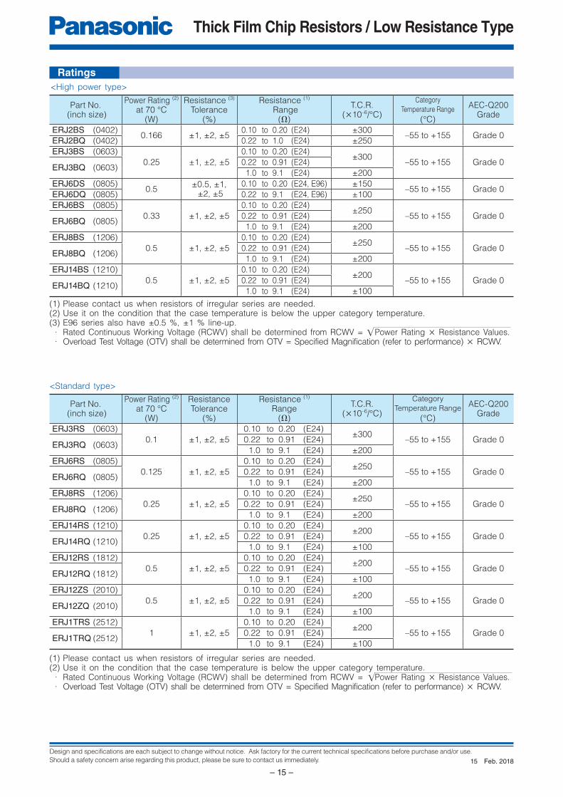
Thick Film Chip Resistors / Low Resistance Type
– 13 –
E
1
R
2
J
3
2
4
B
5 6
W
7
G
8
R
9
0
10
4
11
7
12
X
Thick FilmChip Resistors
Product Code Resistance Tolerance
Code
D
F
G
J
Tolerance
± 0.5 %✽
± 1 %
± 2 %
± 5 %
Shown by 4 digits or letters.
(Ex.) R047 : 0.047 Ω=47m Ω
Resistance Value Packaging Methods
Code Packaging Part No.
XPressed Carrier Taping
2 mm pitch, 10,000 pcs.
ERJ3LWERJ6LWERJ3BWERJ6BWERJ8BWERJ6CWERJ8CW
ERJ2LWERJ2BW
VPunched Carrier Taping
4 mm pitch, 5,000 pcs.
Code Inch
2LW
3LW
6LW
2BW
3BW
6BW
8BW
6CW
8CW
0402
0603
0805
0402
0603
0805
1206
0805
1206
0.2 W
0.25 W
0.5 W
0.25 W
0.33 W
0.5 W
1 W
0.5 W
1 W
Power Rating Resistance Value
10m Ω5m Ω,10m Ω
5, 6, 7, 8, 9m Ω47m Ω to 100m Ω20m Ω to 100m Ω10m Ω to 100m Ω10m Ω to 100m Ω10m Ω to 30m Ω10m Ω to 50m Ω
✽ Please refer to the rating table
for the resistance tolerance
Explanation of Part Numbers
■ As for Packaging Methods, Land Pattern, Soldering Conditions and Safety Precautions, Please see Data Files
Thick Film Chip Resistors / Low Resistance Type
Type: ERJ 2LW, 3LW, 6LW 2BW, 3BW, 6BW, 8BW, 6CW, 8CW ERJ 2B, 3B, 6D, 6B, 8B, 14B, 3R, 6R, 8R, 14R, 12R, 12Z, 1TR ERJ L03, L06, L08, L14, L12, L1D, L1W
● Current Sensing resistor● Small size and lightweight● Realize both low-resistance & High-precision by original thick fi lm resistive element & special electrode structure● Suitable for both refl ow and fl ow sol der ing● Realize High-power by double-sided resistive elements structure that aimed
to suppress temperature rising : ERJ2LW, 3LW, 6LW, 2BW, 3BW, 6BW, 8BW, 6CW, 8CW
● Low TCR : ±75×10–6/°C (ERJ6CW, 8CW)● Low Resistance Value : Thick fi lm resistors available from 5m Ω (ERJ3LW, 6LW)● Reference Standards : IEC 60115-8, JIS C 5201-8, JEITA RC-2144● AEC-Q200 qualifi ed ● RoHS compliant
Features
● ERJ2LW, 3LW, 6LW, 2BW, 3BW, 6BW, 8BW, 6CW, 8CW
<High power (double-sided resistive elements structure) type>
Feb. 201815

Design and specifications are each subject to change without notice. Ask factory for the current technical specifications before purchase and/or use.
Should a safety concern arise regarding this product, please be sure to contact us immediately.
Thick Film Chip Resistors / Low Resistance Type
– 14 –
E
1
R
2
J
3
L
4
1
5
4
6
K
7
J
8
5
9
0
10
M
11
U
12
Thick FilmChip Resistors
Product Code Size, Power Rating
Type Inch
0.2 W
0.25 W
0.33 W
0.33 W
0.5 W
0.5 W
1 W
Power R.
Code
K
U
Resistance Tolerance
Code
F
J
Tolerance
± 1 %
± 5 %
Shown by 3 digits or letters.(Ex.) 50M:50m Ω, 10 C:100m Ω
Resistance Value
Packaging Methods
Code
V
U
Packaging Part No.
Punched Carrier Taping
4 mm pitch, 5,000 pcs.
Embossed Carrier Taping
4 mm pitch, 5,000 pcs.
Embossed Carrier Taping
4 mm pitch, 3,000 pcs.
ERJL03
ERJL06
ERJL08
ERJL14
ERJL12
ERJL1D
ERJL1W
Std.
20m Ω to 100m Ω
Res. Value
L03
L06
L08
L14
L12
L1D
L1W
20m Ω, 22m Ω, 33m Ω,39m Ω, 47m Ω, 50m Ω,100m Ω
✽
✽
✽ L03, L06, L08 : 47m Ω to 100m ΩL1D, L1W : 40m Ω to 100m Ω
0603
0805
1206
1210
1812
2010
2512
E
1
R
2
J
3
8
4
R
5 6
Q
7
F
8
R
9
2
10
2
11
V
Thick Film
Chip Resistors
Product Code Size, Power Rating
Type
0.166 W
0.25 W
0.1 W
0.5 W
0.33 W
0.125 W
0.5 W
0.25 W
0.5 W
0.25 W
0.5 W
0.5 W
1 W
Power R.
Resistance Value
Code
S
Q
0.1 Ω to 0.2 Ω
0.22 Ω to 9.1 Ω✽
Resistance Tolerance
Code
D
F
G
J
Tolerance
± 0.5 %✽
± 1 %
± 2 %
± 5 %
Shown by 3 digits or letters.Only when it is D (E24,E96) or F (E96), shown by 4 digits or letters.(Ex.) R22 : 0.22 Ω R102 : 0.102 Ω
Resistance Value
Packaging Methods
Code Packaging Part No.
Punched Carrier Taping4 mm pitch, 5,000 pcs.
Embossed Carrier Taping4 mm pitch, 5,000 pcs.
2B
3B
3R
6D
6B
6R
8B
8R
14B
14R
12R
12Z
1TR
Res. Value
V
X
U
Punched Carrier Taping2 mm pitch, 10,000 pcs.
Embossed Carrier Taping4 mm pitch, 4,000 pcs.
ERJ2B
ERJ3B/3R
ERJ6D/6B/6R
ERJ8B/8R
ERJ14B/14R
ERJ12R
ERJ12Z
ERJ1TR
✽ 2B : 0.22 Ω to 1.0 Ω
Inch
0402
0603
0603
0805
0805
0805
1206
1206
1210
1210
1812
2010
2512
✽ Please refer to the rating table for the resistance tolerance
● ERJL03, L06, L08, L14, L12, L1D, L1W <Low TCR type>
<High power (double-sided resistive elements structure) type>
(1) Please contact us when resistors of irregular series are needed.(2) Use it on the condition that the case temperature is below the upper category temperature. · Rated Continuous Working Voltage (RCWV) shall be determined from RCWV = Power Rating × Resistance Values. · Overload Test Voltage (OTV) shall be determined from OTV = Specified Magnification (refer to performance) × RCWV.
Part No. (inch size)
Power Rating (2)
at 70 °C(W)
ResistanceTolerance
(%)
Resistance (1)
Range(Ω)
T.C.R.(×10–6/°C)
CategoryTemperature Range
(°C)
AEC-Q200Grade
ERJ2LW (0402) 0.2 ±1, ±2, ±5 10m 0 to 500 –55 to +125 Grade 1
ERJ3LW (0603) 0.25 ±1, ±2, ±5 5m 0 to 700 –55 to +125
Grade 110m 0 to 300 –55 to +125
ERJ6LW (0805) 0.5 ±1, ±2, ±5 5, 6, 7, 8, 9m 0 to 300 –55 to +125 Grade 1
ERJ2BW (0402) 0.25 ±1, ±2, ±5 47m to 100m (E24) ±300 –55 to +155 Grade 0
ERJ3BW (0603) 0.33 ±1, ±2, ±5 20m to 100m (E24)20m Ω ≤ R < 39m Ω : ±25039m Ω ≤ R ≤ 100m Ω : ±150
–55 to +155 Grade 0
ERJ6BW (0805) 0.5 ±1, ±2, ±5 10m to 100m (E24)10m Ω ≤ R < 15m Ω : ±30015m Ω ≤ R ≤ 100m Ω : ±200
–55 to +155 Grade 0
ERJ8BW (1206) 1 ±1, ±2, ±5 10m to 100m (E24)10m Ω ≤ R < 20m Ω : ±20020m Ω ≤ R < 47m Ω : ±15047m Ω ≤ R ≤ 100m Ω : ±100
–55 to +155 Grade 0
ERJ6CW (0805) 0.5 ±0.5, ±1, ±2, ±5 10m to 30m (E24) ±75 –55 to +125 Grade 1
ERJ8CW (1206) 1 ±1, ±2, ±5 10m to 50m (E24) ±75 –55 to +125 Grade 1
● ERJ2BS/2BQ, 3BS/3BQ, 6BS/6BQ, 8BS/8BQ, 14BS/14BQ, 6D, 3R, 6R, 8R, 14R, 12R, 12Z, 1TR
<High power type/Standard type>
Ratings
√
Feb. 201815
Design and specifications are each subject to change without notice. Ask factory for the current technical specifications before purchase and/or use.
Should a safety concern arise regarding this product, please be sure to contact us immediately.
Thick Film Chip Resistors / Low Resistance Type
– 15 –
Part No. (inch size)
Power Rating (2)
at 70 °C(W)
ResistanceTolerance
(%)
Resistance (1)
Range(Ω)
T.C.R.(×10–6/°C)
Category
Temperature Range
(°C)
AEC-Q200Grade
ERJ3RS (0603)
0.1 ±1, ±2, ±5
0.10 to 0.20 (E24)±300
–55 to +155 Grade 0ERJ3RQ (0603)
0.22 to 0.91 (E24)
1.0 to 9.1 (E24) ±200
ERJ6RS (0805)
0.125 ±1, ±2, ±5
0.10 to 0.20 (E24)±250
–55 to +155 Grade 0ERJ6RQ (0805)
0.22 to 0.91 (E24)
1.0 to 9.1 (E24) ±200
ERJ8RS (1206)
0.25 ±1, ±2, ±5
0.10 to 0.20 (E24)±250
–55 to +155 Grade 0ERJ8RQ (1206)
0.22 to 0.91 (E24)
1.0 to 9.1 (E24) ±200
ERJ14RS (1210)
0.25 ±1, ±2, ±5
0.10 to 0.20 (E24)±200
–55 to +155 Grade 0ERJ14RQ (1210)
0.22 to 0.91 (E24)
1.0 to 9.1 (E24) ±100
ERJ12RS (1812)
0.5 ±1, ±2, ±5
0.10 to 0.20 (E24)±200
–55 to +155 Grade 0ERJ12RQ (1812)
0.22 to 0.91 (E24)
1.0 to 9.1 (E24) ±100
ERJ12ZS (2010)
0.5 ±1, ±2, ±5
0.10 to 0.20 (E24)±200
–55 to +155 Grade 0ERJ12ZQ (2010)
0.22 to 0.91 (E24)
1.0 to 9.1 (E24) ±100
ERJ1TRS (2512)
1 ±1, ±2, ±5
0.10 to 0.20 (E24)±200
–55 to +155 Grade 0ERJ1TRQ (2512)
0.22 to 0.91 (E24)
1.0 to 9.1 (E24) ±100
<Standard type>
(1) Please contact us when resistors of irregular series are needed.(2) Use it on the condition that the case temperature is below the upper category temperature.(3) E96 series also have ±0.5 %, ±1 % line-up. · Rated Continuous Working Voltage (RCWV) shall be determined from RCWV = Power Rating × Resistance Values. · Overload Test Voltage (OTV) shall be determined from OTV = Specified Magnification (refer to performance) × RCWV.
(1) Please contact us when resistors of irregular series are needed.(2) Use it on the condition that the case temperature is below the upper category temperature. · Rated Continuous Working Voltage (RCWV) shall be determined from RCWV = Power Rating × Resistance Values. · Overload Test Voltage (OTV) shall be determined from OTV = Specified Magnification (refer to performance) × RCWV.
<High power type>
Ratings
Part No. (inch size)
Power Rating (2)
at 70 °C(W)
Resistance (3)
Tolerance(%)
Resistance (1)
Range(Ω)
T.C.R.(×10–6/°C)
Category
Temperature Range
(°C)
AEC-Q200Grade
ERJ2BS (0402)0.166 ±1, ±2, ±5
0.10 to 0.20 (E24) ±300–55 to +155 Grade 0
ERJ2BQ (0402) 0.22 to 1.0 (E24) ±250
ERJ3BS (0603)
0.25 ±1, ±2, ±5
0.10 to 0.20 (E24)±300
–55 to +155 Grade 0ERJ3BQ (0603)
0.22 to 0.91 (E24)
1.0 to 9.1 (E24) ±200
ERJ6DS (0805)0.5
±0.5, ±1, ±2, ±5
0.10 to 0.20 (E24, E96) ±150–55 to +155 Grade 0
ERJ6DQ (0805) 0.22 to 9.1 (E24, E96) ±100
ERJ6BS (0805)
0.33 ±1, ±2, ±5
0.10 to 0.20 (E24)±250
–55 to +155 Grade 0ERJ6BQ (0805)
0.22 to 0.91 (E24)
1.0 to 9.1 (E24) ±200
ERJ8BS (1206)
0.5 ±1, ±2, ±5
0.10 to 0.20 (E24)±250
–55 to +155 Grade 0ERJ8BQ (1206)
0.22 to 0.91 (E24)
1.0 to 9.1 (E24) ±200
ERJ14BS (1210)
0.5 ±1, ±2, ±5
0.10 to 0.20 (E24)±200
–55 to +155 Grade 0ERJ14BQ (1210)
0.22 to 0.91 (E24)
1.0 to 9.1 (E24) ±100
√
√
Feb. 201815

Design and specifications are each subject to change without notice. Ask factory for the current technical specifications before purchase and/or use.
Should a safety concern arise regarding this product, please be sure to contact us immediately.
Thick Film Chip Resistors / Low Resistance Type
– 16 –
–40 –20 0 20 40 60 80 100 120 140 1600
180–60
155 °C
70 °C
Ambient Temperature (°C)
20
40
60
80
100
Rate
d L
oad
(%
)
–55 °C
125 °C
Protective coating
Alumina
substrate
Electrode (Inner)
Electrode(Between)
Electrode (Outer)Thick filmresistive element
a
b
t
W
L
Power Derating CurveFor resistors operated in ambient temperatures above 70 °C, power rating shall be derated in accordance with the figure below.
Dimensions in mm (not to scale)
Construction
Part No. (inch size)
Power Rating (2)
at 70 °C(W)
ResistanceTolerance
(%)
Resistance (1)
Range(Ω)
T.C.R.(×10–6/°C)
CategoryTemperature Range
(°C)
AEC-Q200Grade
ERJL03 (0603) 0.2 ±1, ±5 47m to 100m ±200 –55 to +125 Grade 1
ERJL06 (0805) 0.25 ±1, ±5 47m to 100m ±100 –55 to +125 Grade 1
ERJL08 (1206) 0.33 ±1, ±5 47m to 100m ±100 –55 to +125 Grade 1
ERJL14 (1210) 0.33 ±1, ±5 20m to 100m
R < 47m Ω : ±300
R ≥ 47m Ω : ±100
–55 to +125 Grade 1
ERJL12 (1812) 0.5 ±1, ±5 20m to 100m –55 to +125 Grade 1
ERJL1D (2010) 0.5 ±1, ±5 40m to 100m –55 to +125 Grade 1
ERJL1W (2512) 1 ±1, ±5 40m to 100m –55 to +125 Grade 1
<Low TCR type>
(1) Standard R.V. : 20m Ω, 22m Ω, 33m Ω, 39m Ω, 47m Ω, 50m Ω, 100m Ω, Custom R.V. : Each 1m Ω within upper range.(2) Use it on the condition that the case temperature is below the upper category temperature. ∙ Rated Continuous Working Voltage (RCWV) shall be determined from RCWV = Power Rating × Resistance Values. · Overload Test Voltage (OTV) shall be determined from OTV = Specified Magnification (refer to performance) × RCWV.
√
Part No.Dimensions (mm) Mass(Weight)
[g/1000 pcs.]L W a b t
ERJ2LW 1.00±0.10
0.50+0.10
0.25±0.10
0.25±0.10
0.40±0.05
0.8
ERJ2BW 1.00±0.10
0.50+0.10
0.24±0.10
0.24±0.10
0.35±0.05
0.8
ERJ2BS1.00
±0.100.50
+0.100.20
±0.100.27
±0.100.35
±0.050.8
ERJ2BQ
ERJ3LW(5m Ω)
1.60±0.15 0.80±0.15 0.50±0.20 0.50±0.20 0.55±0.10 3
ERJ3LW(10m Ω)
ERJ3BW1.60±0.15 0.80±0.15 0.40±0.20 0.40±0.20 0.55±0.10 3
ERJ3R
1.60±0.15 0.80+0.15
0.30±0.20 0.30±0.15 0.45±0.10 2ERJ3B
ERJL03
ERJ6LW 2.00±0.20 1.25±0.20 0.63±0.20 0.63±0.20 0.70±0.10 6
ERJ6BW 2.00±0.20 1.25±0.20 0.55±0.20 0.55±0.20 0.65±0.10 6
ERJ6CW(10 to 13m Ω)
2.05±0.20 1.30±0.20
0.60±0.20 0.60±0.20
0.65±0.10 6ERJ6CW(15 to 30m Ω)
0.45±0.20 0.45±0.20
ERJ6D 2.00±0.20 1.25±0.10 0.40±0.20 0.55±0.25 0.60±0.10 5
ERJ6R
2.00±0.20 1.25±0.10 0.40±0.20 0.40±0.20 0.60±0.10 5ERJ6B
ERJL06
–0.05
–0.05
–0.05
–0.05
Part No.Dimensions (mm) Mass(Weight)
[g/1000 pcs.]L W a b t
ERJ8BW 3.20±0.20 1.60±0.20 1.00±0.20 1.00±0.20 0.65±0.10 13
ERJ8CW(10 to 16m Ω)
3.20±0.20 1.60±0.20 1.10±0.20 1.10±0.20 0.65±0.10 13
ERJ8CW(18 to 50m Ω)
3.20±0.20 1.60±0.20 0.60±0.20 0.60±0.20 0.65±0.10 13
ERJ8R
3.20+0.05
1.60+0.05
0.50±0.20 0.50±0.20 0.60±0.10 10ERJ8B
ERJL08
ERJ14R
3.20±0.20 2.50±0.20 0.50±0.20 0.50±0.20 0.60±0.10 16ERJ14B
ERJL14
ERJ12R4.50±0.20 3.20±0.20 0.50±0.20 0.50±0.20 0.60±0.10 27
ERJL12
ERJ12ZERJL1D
5.00±0.20
2.50±0.20
0.60±0.20
0.60±0.20
0.60±0.10
27
ERJ1TR 6.40±0.20
3.20±0.20
0.65±0.20
0.60±0.20
0.60±0.10
45
ERJL1W 6.40±0.20
3.20±0.20
0.65±0.20
1.30±0.20
1.10±0.10
79
–0.20 –0.15
Feb. 201815

Design and specifications are each subject to change without notice. Ask factory for the current technical specifications before purchase and/or use.
Should a safety concern arise regarding this product, please be sure to contact us immediately.
Thick Film Chip Resistors / Low Resistance Type
– 17 –
Test ItemPerformance
RequirementsTest Conditions
ResistanceWithin Specifi ed
Tolerance20 °C
T. C. R.Within Specifi ed
T. C. R.+25 °C/+125 °C
Overload ±2%
Rated Voltage × 2.0, 5 s
ERJ6LW : × 1.77, 5 s
ERJ8BW (R > 0.05 Ω) : × 1.77, 5 s
Resistance to Soldering Heat ±1% 270 °C, 10 s
Rapid Change of
Temperature±1%
ERJ2LW : ±2%–55 °C (30 min.) / +155 °C (ERJ✽LW, ERJ✽CW : +125 °C) (30 min.), 100 cycles
High Temperature Exposure ±1% +155 °C (ERJ✽LW, ERJ✽CW : +125 °C), 1000 h
Damp Heat, Steady State ±1% 60 °C, 90% to 95%RH, 1000 h
Load Life in Humidity ±3%60 °C, 90% to 95%RH, Rated Voltage,
1.5 h ON/0.5 h OFF cycle, 1000 h
Endurance at 70 °C ±3% 70 °C, Rated Voltage, 1.5 h ON/0.5 h OFF cycle, 1000 h
Test ItemPerformance
RequirementsTest Conditions
ResistanceWithin Specifi ed
Tolerance20 °C
T. C. R.Within Specifi ed
T. C. R.+25 °C/+125 °C
Overload ±2% Rated Voltage × 2.5 (ERJ6D : × 1.77), 5 s
Resistance to Soldering Heat ±1% 270 °C, 10 s
Rapid Change of
Temperature±1% –55 °C (30 min.) / +155 °C (30 min.), 100 cycles
High Temperature Exposure ±1% +155 °C, 1000 h
Damp Heat, Steady State ±1% 60 °C, 90% to 95%RH, 1000 h
Load Life in Humidity ±3%60 °C, 90% to 95%RH, Rated Voltage,
1.5 h ON/0.5 h OFF cycle, 1000 h
Endurance at 70 °C ±3% 70 °C, Rated Voltage, 1.5 h ON/0.5 h OFF cycle, 1000 h
Test ItemPerformance
RequirementsTest Conditions
ResistanceWithin Specifi ed
Tolerance20 °C
T. C. R.Within Specifi ed
T. C. R.+25 °C/+125 °C
Overload ±2% Rated Voltage × 2.5, 5 s
Resistance to Soldering Heat ±1% 270 °C, 10 s
Rapid Change of
Temperature±1% –55 °C (30 min.) / +125 °C (30 min.), 100 cycles
High Temperature Exposure ±1% +125 °C, 1000 h
Damp Heat, Steady State ±1% 60 °C, 90% to 95%RH, 1000 h
Load Life in Humidity ±3%60 °C, 90% to 95%RH, Rated Voltage,
1.5 h ON/0.5 h OFF cycle, 1000 h
Endurance at 70 °C ±3% 70 °C, Rated Voltage, 1.5 h ON/0.5 h OFF cycle, 1000 h
● ERJ2LW, 3LW, 6LW, 2BW, 3BW, 6BW, 8BW, 6CW, 8CW
<High power (double-sided resistive elements structure) type>
● ERJ2BS/2BQ, 3BS/3BQ, 6BS/6BQ, 8BS/8BQ, 14BS/14BQ, 6D, 3R, 6R, 8R, 14R, 12R, 12Z, 1TR
<High power type/Standard type>
● ERJL03, L06, L08, L14, L12, L1D, L1W <Low TCR type>
Performance
Feb. 201815

Design and specifications are each subject to change without notice. Ask factory for the current technical specifications before purchase and/or use.
Should a safety concern arise regarding this product, please be sure to contact us immediately.
Current Sensing Resistors, Metal Plate Type
– 18 –
E
1
R
2
J
3
M
4
S
5
4
6 7
S
8
F
9
2
10
M
11
0
12
U
Product Code Resistance Value Packaging Methods
Code Packaging
Embossed Carrier Taping4 mm pitch, 3,000 pcs.
U
Part No.
ERJMS4
ERJMB1
Embossed Carrier Taping4 mm pitch, 2,000 pcs.
Metal PlateChip Resistors
Resistance Tolerance
Tolerance
±1 %
Shown by 3 digits or
letters.Decimal point
is expressed by M as
2.0m Ω=2M0,
0.5m Ω=M50,
10.0m Ω=10M
Code
F
Type Code
Inch size
2512
2512
2526
1020
Electrode type
Standard
Narrow
Standard
Standard
Code
S4S
S4H
S6S
B1S
Embossed Carrier Taping8 mm pitch, 1,000 pcs.
ERJMS6
–40 0 40 80 120 1600
200–80
100 °C−65 °C 130 °C
170 °C
Terminal Temperature (°C)
20
40
60
100
80
120
Rate
d L
oad
(%
)
ERJMS4H(7 to 10m Ω)
Current Sensing Resistors, Metal Plate Type
Type: ERJ MS4, MS6, MB1
Explanation of Part Numbers
● Ideal for current sensing solution● Small case size with high power ● Metal plate bonding technology. Excellent long term stability● Outer Resin with high heat dissipation. Wide temperature range (-65 °C to +170 °C) ● AEC-Q200 qualifi ed ● RoHS compliant● ISO9001, ISO/TS16949 certifi ed
■ As for Packaging Methods, Soldering Conditions and Safety Precautions, Please see Data Files
Part No.(inch size)
Power Ratingat 70 °C
(W)
ResistanceRange(mΩ)
ResistanceTolerance
(%)
T.C.R.(×10–6/°C)
CategoryTemperature Range
(°C)
Terminal temp.upper limit
(°C)
ERJMS4S(2512)
3 1, 2, 3, 4 F : ±1 ±75 –65 to +170 130
ERJMS4H(2512)
3 5, 6 F : ±1 ±75 –65 to +170 130
2 7, 8, 9, 10 F : ±1 ±75 –65 to +170 100
ERJMS6S(2526)
5 0.5, 1, 2 F : ±1 ±75 –65 to +170 130
ERJMB1S(1020)
2 1, 2, 3, 4, 5 F : ±1 ±75 –65 to +170 130
✽ Please contact us when resistors of irregular series are needed.
<Supplemented>In the case of the temperature measurement of the terminal portion of the resistor, Please perform under the following conditions.
1) Tarminal temperature measurement, please apply the temperature of the higher of either the left or right electrode upper surface of the resistor.
2) Please measure the temperature of the resistor in the land pattern printed of circuit board and plan to use by real conditions.
Power Derating CurveIf the terminal temperature of the resistor is more than terminal temperature upper limit value of the rated table, please reduce the rated power according to the Power Derating Curve shown in the figure on the right.
Features
Ratings
Oct. 201604

Design and specifications are each subject to change without notice. Ask factory for the current technical specifications before purchase and/or use.
Should a safety concern arise regarding this product, please be sure to contact us immediately.
Current Sensing Resistors, Metal Plate Type
– 19 –
Resistive Element (Metal Plate)
Protective Film
Surface Treatment (Ni/Sn)
Electrode (Metal)
LA
W
LA
t
W
t
ac
b
ac
b
LA
W
t
ac
b
Land Pattern
–1
–0.5
0
0.5
1
–80 –60 –40 –20 0 20 40 60 80 100 120 140 160 180
Chang
e o
f R
esis
tance (
%)
Temperature (°C)
–1
–0.5
0
0.5
1
2000
ERJMS4SF2M0U 140 °C Storage
0 4000 6000 8000
Chang
e o
f R
esis
tance (
%)
Test Time (hrs)
● ERJMS4S/ERJMS4H ● ERJMS6S ● ERJMB1S
Construction
Dimensions in mm (not to scale), Recommended Land Pattern
Part No.(inch size)
Dimension (mm) Recommended Land Pattern (mm) Mass (Weight)(g/1000 pcs.)L W A t a b c
ERJMS4S(2512)
6.40±0.25 3.20±0.25 2.20±0.25 1.20±0.15 2.7 3.4 2.0 120
ERJMS4H(2512)
6.40±0.25 3.20±0.25 1.25±0.25 1.20±0.15 1.7 3.4 4.0 115
ERJMS6S(2526)
6.40±0.25 6.80±0.25 2.20±0.25 1.20±0.15 2.7 7.0 2.0 260
ERJMB1S(1020)
2.55±0.25 5.00±0.25 0.68+0.15 0.90±0.15 1.15 5.5 1.1 40−0.20
Typical Temperature dependence of electrical resistance Long-term stability
Oct. 201604
Design and specifications are each subject to change without notice. Ask factory for the current technical specifications before purchase and/or use.
Should a safety concern arise regarding this product, please be sure to contact us immediately.
Current Sensing Resistors, Metal Plate Type
– 20 –
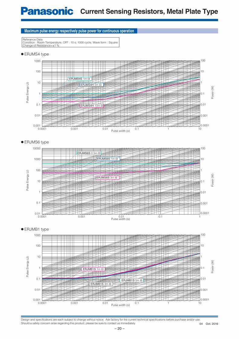
Maximum pulse energy respectively pulse power for continuous operation
0.0001 0.001 0.01 0.1 1 100.0001
0.001
0.01
0.1
1
10
1001000
100
10
1
0.1
0.01
0.001
Pulse width (s)
Po
we
r (W
)
Pu
lse
En
erg
y (
J)
ERJMS4S 1m Ω
ERJMS4H 5m Ω
ERJMS4H 10m Ω
0.0001 0.001 0.01 0.1 10.0001
0.001
0.01
0.1
1
10
100
100
1000
10000
10
1
0.1
0.01
Pulse width (s)
Pow
er
(W)
Puls
e E
nerg
y (
J)
ERJMS6S 0.5m Ω
ERJMS6S 1m Ω
ERJMS6S 3m Ω
0.0001 0.001 0.01 0.1 1 100.0001
0.001
0.01
0.1
1
10
1001000
100
10
1
0.1
0.01
0.001
Pulse width (s)
Pow
er
(W)
Puls
e E
nerg
y (
J)
ERJMB1S 5m ΩERJMB1S 3m Ω
ERJMB1S 1m Ω
Referance DataCondition : Room Temperature, OFF : 10 s, 1000 cycle, Wave form : SquareChange of Resistance=±1 %
● ERJMS4 type
● ERJMS6 type
● ERJMB1 type
Oct. 201604

Design and specifications are each subject to change without notice. Ask factory for the current technical specifications before purchase and/or use.
Should a safety concern arise regarding this product, please be sure to contact us immediately.
Current Sensing Resistors, Metal Plate Type
– 21 –
温度上昇
(°C
)
電力 (W)
00
10
20
30
40
50
60
70
80
90
100
1 2 3
Tem
pera
ture
Ris
e (
°C)
Power (W)
00
10
20
30
40
50
60
70
80
90
100
1 432 5
Tem
pera
ture
Ris
e (
°C)
Power (W)
00
10
20
30
40
50
60
70
80
1 2
Resistor Soldering
PWB
21
Sense terminal
Land
<Condition>
Base material : FR-4 (t1.6mm) Copper Thickness : 70 μm, Two layer2
1
● ERJMS4, ERJMS6 type
Performance (AEC-Q200)
Temperature Rise
● ERJMS4HF5M0U ● ERJMS6SF2M0U ● ERJMB1SF3M0U
● ERJMB1 type
Test Item Test Condition Specification Typical value
Thermal Shock −55 °C/155 °C, 1000cycles ±1 % 0.20 %
Overload 3 × Rated Power, 5 sec ±0.5 % 0.10 %
Solderability 245 °C, 3 sec > 95% coverage > 95% coverage
Resistance to Solvents MIL-STD-202 method 215, 2.1a, 2.1d No damage No damage
Low Temperature Storage and Operation −65 °C, 24 h ±0.5 % 0.03 %
Resistance to Soldering Heat MIL-STD-202 method 210 (260 °C, 10s) ±0.5 % 0.10 %
Moisture Resistance MIL-STD-202 method 106 ±0.5 % 0.10 %
Shock MIL-STD-202 method 213-A ±0.5 % 0.10 %
Vibration, High Frequency 10 to 2000 (Hz) ±0.5 % 0.05 %
Life 70 °C, Rated Power, 2000 h ±1 % 0.30 %
Storage Life at Elevated Temperature 170 °C, 2000 h ±1 % 0.30 %
High Temperature Characteristics 140 °C, 2000 h ±0.5 % 0.05 %
Frequency Characteristics Inductance < 5 nH < 2 nH
Test Item Test Condition Specification Typical value
Thermal Shock −55 °C/155 °C, 1000cycles ±1 % 0.30 %
Overload 2.5 × Rated Power, 5 sec ±1 % 0.30 %
Solderability 245 °C, 3 sec > 95% coverage > 95% coverage
Resistance to Solvents MIL-STD-202 method 215, 2.1a, 2.1d No damage No damage
Low Temperature Storage and Operation −65 °C, 24 h ±0.5 % 0.03 %
Resistance to Soldering Heat MIL-STD-202 method 210 (260 °C, 10s) ±0.5 % 0.10 %
Moisture Resistance MIL-STD-202 method 106 ±0.5 % 0.10 %
Shock MIL-STD-202 method 213-A ±0.5 % 0.10 %
Vibration, High Frequency 10 to 2000 (Hz) ±0.5 % 0.05 %
Life 70 °C, Rated Power, 2000 h ±1 % 0.30 %
Storage Life at Elevated Temperature 170 °C, 2000 h ±1 % 0.30 %
High Temperature Characteristics 140 °C, 2000 h ±0.5 % 0.05 %
Frequency Characteristics Inductance < 5 nH < 2 nH
Sense terminal-Layout
Oct. 201604
Design and specifications are each subject to change without notice. Ask factory for the current technical specifications before purchase and/or use.
Should a safety concern arise regarding this product, please be sure to contact us immediately.
Current Sensing Resistors, Metal Plate Type
– 22 –
E
1
R
2
J
3
M
4
1
5
W
6
S
7
F
8
3
9
M
10
0
11
U
12
Product Code Size, Power Rating
Code
M1W 1 W
Power R.
Code
S
T
Type
General type
Wide terminal type
Resistance Tolerance
Code
F
J
Tolerance
± 1 %
± 5 %
Shown by 3 digits or letters.Decimal point is expressed by M as 3 mΩ=3M0, 10 mΩ=10M
Resistance Value
Packaging Methods
Code
U
Packaging
Embossed Carrier Taping
4 mm pitch, 3,000 pcs.
Thick FilmChip Resistors
Inch
2512
120
100
80
60
40
20
0–55 –40 0 40 80
70 °C
120 160
170 °C
200
Ambient Temperature (°C)
Rate
d L
oad
(%
)
155 °C
■ As for Packaging Methods, Soldering Conditions and Safety Precautions, Please see Data Files
Features
Current Sensing Resistors, Metal Plate Type
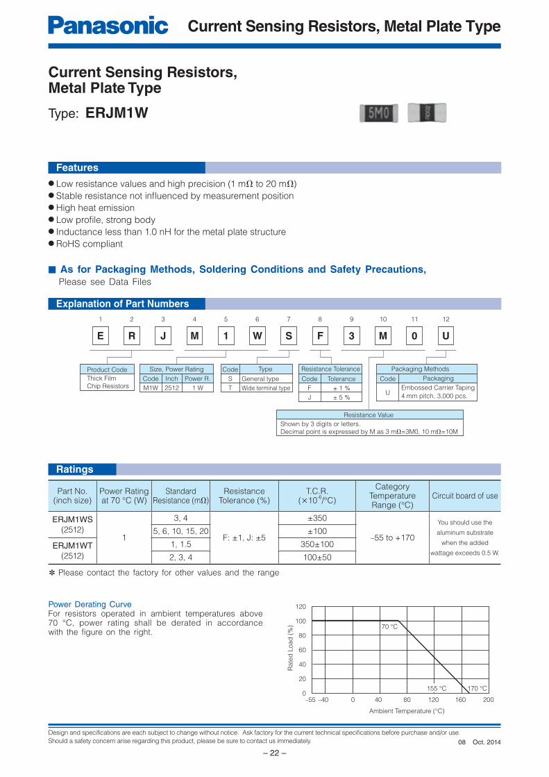
Type: ERJM1W
● Low resistance values and high precision (1 mΩ to 20 mΩ)● Stable resistance not infl uenced by measurement position● High heat emission● Low profi le, strong body● Inductance less than 1.0 nH for the metal plate structure● RoHS compliant
✽ Please contact the factory for other values and the range
Explanation of Part Numbers
Ratings
Power Derating CurveFor resistors operated in ambient temperatures above 70 °C, power rating shall be derated in accordance with the figure on the right.
Part No.(inch size)
Power Ratingat 70 °C (W)
StandardResistance (mΩ)
ResistanceTolerance (%)
T.C.R.(×10
-6/°C)
CategoryTemperatureRange (°C)
Circuit board of use
ERJM1WS
(2512)1
3, 4
F: ±1, J: ±5
±350
–55 to +170
You should use the
aluminum substrate
when the added
watt age exceeds 0.5 W.
5, 6, 10, 15, 20 ±100
ERJM1WT
(2512)
1, 1.5 350±100
2, 3, 4 100±50
Oct. 201408

Design and specifications are each subject to change without notice. Ask factory for the current technical specifications before purchase and/or use.
Should a safety concern arise regarding this product, please be sure to contact us immediately.
Current Sensing Resistors, Metal Plate Type
– 23 –
L
WT
a
a
b
c
Wiring pattern(copper trace)
Land pattern
Solder resist
Terminal; Plated Metal
Resistive Body; Alloy Plate
Protective coating; Resin
Construction Dimensions in mm (not to scale)
● An example of a land pattern
Part No.Dimensions (mm)
a b c
ERJM1WS 2.1 3.4 4.2
ERJM1WT 3.1 3.4 2.2
TypePart No.
(inch size)
Dimensions (mm)
L W T aMass (Weight)[g/1000 pcs.]
S TypeERJM1WS
(2512)6.40±0.25
3.20±0.25 0.80±0.30
1.00±0.25 70
T TypeERJM1WT
(2512)6.40±0.40 2.10±0.30 90
Recommended Land Pattern
Oct. 201408

Design and specifications are each subject to change without notice. Ask factory for the current technical specifications before purchase and/or use.
Should a safety concern arise regarding this product, please be sure to contact us immediately.
Current Sensing Resistors, Metal Foil Type
– 24 –
E
1
R
2
J
3
M
4
F
5
B
6 7
A
8
F
9
1
10
0
11
M
12
X
Product Code Resistance Value Packaging Methods
Code Packaging
XPunched Carrier Taping2 mm pitch, 10,000 pcs.
Metal FoilChip Resistors
Shown by 3 digits or letters.
Decimal point is expressed
by M as
Size, Power Rating
Power R.
0.33 W
Code
BA
Inch
0402
Resistance Tolerance
Tolerance
±1 %
Code
F
5M0=5m Ω10M=10m Ω
–40 –20 0 806020 12010040 1601400
180–60
Ambient Temperature (°C)
20
40
60
100
80
120
Rate
d P
ow
er
(%)
70 °C−55 °C
125 °C
■ As for Packaging Methods, Soldering Conditions and Safety Precautions, Please see Data Files
Current Sensing Resistors, Metal Foil Type
Type: ERJ MFBA
● Suitable for current sensing for smartphones and other small devices● Unique metal foil process achieved high power and low temperature coeffi cient● RoHS compliant ● ISO9001 certifi ed
Features
Ratings
Power Derating CurveIf the ambient temperature of the resistor is more than ambient temperature upper limit value of the rated table, please reduce the rated power according to the Power Derating Curve shown in the figure on the right.
Explanation of Part Numbers
Part No.(inch size)
Power Ratingat 70 °C
(W)
ResistanceRange✽
(mΩ)
ResistanceTolerance
(%)
T.C.R.(×10–6/°C)
CategoryTemperature Range
(°C)
ERJMFBA(0402)
0.33 5, 10, 20 F : ±1 ±150 –55 to +125
✽ Use it on the condition that the case temperature is below 125 °C.
Jan. 201800
Design and specifications are each subject to change without notice. Ask factory for the current technical specifications before purchase and/or use.
Should a safety concern arise regarding this product, please be sure to contact us immediately.
Current Sensing Resistors, Metal Foil Type
– 25 –
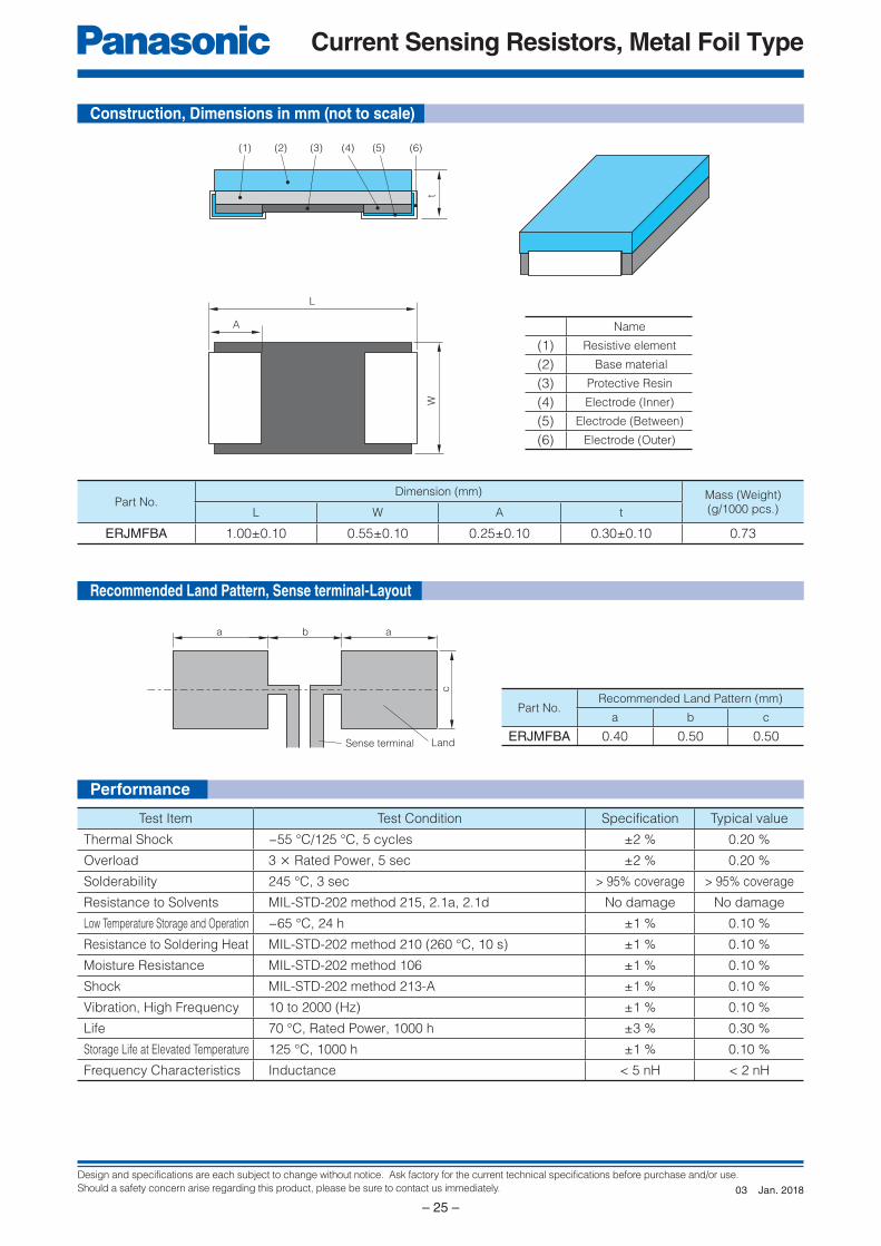
(1) (2) (3)
L
tW
A
(4) (5) (6)
Part No.Dimension (mm) Mass (Weight)
(g/1000 pcs.)L W A t
ERJMFBA 1.00±0.10 0.55±0.10 0.25±0.10 0.30±0.10 0.73
Part No.Recommended Land Pattern (mm)
a b c
ERJMFBA 0.40 0.50 0.50
Name
(1) Resistive element
(2) Base material
(3) Protective Resin
(4) Electrode (Inner)
(5) Electrode (Between)
(6) Electrode (Outer)
Sense terminal Land
a a
c
b
Performance
Construction, Dimensions in mm (not to scale)
Recommended Land Pattern, Sense terminal-Layout
Test Item Test Condition Specification Typical value
Thermal Shock −55 °C/125 °C, 5 cycles ±2 % 0.20 %
Overload 3 × Rated Power, 5 sec ±2 % 0.20 %
Solderability 245 °C, 3 sec > 95% coverage > 95% coverage
Resistance to Solvents MIL-STD-202 method 215, 2.1a, 2.1d No damage No damage
Low Temperature Storage and Operation −65 °C, 24 h ±1 % 0.10 %
Resistance to Soldering Heat MIL-STD-202 method 210 (260 °C, 10 s) ±1 % 0.10 %
Moisture Resistance MIL-STD-202 method 106 ±1 % 0.10 %
Shock MIL-STD-202 method 213-A ±1 % 0.10 %
Vibration, High Frequency 10 to 2000 (Hz) ±1 % 0.10 %
Life 70 °C, Rated Power, 1000 h ±3 % 0.30 %
Storage Life at Elevated Temperature 125 °C, 1000 h ±1 % 0.10 %
Frequency Characteristics Inductance < 5 nH < 2 nH
Jan. 201803

Design and specifications are each subject to change without notice. Ask factory for the current technical specifications before purchase and/or use.
Should a safety concern arise regarding this product, please be sure to contact us immediately.
High Power Chip Resistors / Wide Terminal Type
– 26 –
E
1
R
2
J
3
A
4
1
5
A
6 7
J
8
1
9
0
10
2
11
U
Thick FilmChip Resistors
Product Code Size, Power Rating
Code
A1
B1
B2
B3
Resistance Value Region
A
B
C
D
Resistance Value
Packaging Methods
VERJB2
ERJB3
ERJA1
Code Packaging Part No.
Punched Carrier Taping
4 mm pitch, 5,000 pcs.
Embossed Carrier Taping
4 mm pitch, 5,000 pcs.
Embossed Carrier Taping
4 mm pitch, 4,000 pcs.
10 Ω
0.22 Ω
0.01 Ω
0.005 Ω
≤ R
≤ R <10 Ω
≤ R < 0.22 Ω
≤ R < 0.01 Ω
Resistance Tolerance
F
G
J
± 1 %
± 2 %
± 5 %
Shown by 3 digits or letters. Only when it is impossible, shown by 4 digits or letters.
Power R.
1.33 W
1 W,2 W(R ≤ 10 Ω)
0.75 W,1 W(R ≤ 10 Ω)
0.33 W,0.5 W(R ≤ 1 Ω)
U
ERJB1
(Ex.) 102 : 1.0k Ω 4R7 : 4.7 Ω
R01 : 0.01 Ω = 10m ΩR015 : 0.015 Ω = 15m Ω
Inch
1225
1020
0612
0508
High Power Chip Resistors / Wide Terminal Type
Type: ERJ A1, B1, B2, B3
● High solder-joint reliability by wide terminal con struc tion● Excellent heat dissipation characteristics by wide terminal construction● AEC-Q200 qualifi ed● RoHS compliant
● Automotive electronic circuits including ECUs (Electrical control unit), anti-lock breaking systems and air-bag systems ● Current sensing for power supply circuits in a variety of equipment
■ As for Packaging Methods, Land Pattern, Soldering Conditions and Safety Precautions, Please see Data Files
Features
Recommended Applications
Explanation of Part Numbers
Oct. 201707

Design and specifications are each subject to change without notice. Ask factory for the current technical specifications before purchase and/or use.
Should a safety concern arise regarding this product, please be sure to contact us immediately.
High Power Chip Resistors / Wide Terminal Type
– 27 –
Protective coating
Thick filmresistive element
Electrode (Inner) Electrode (Between)
Electrode (Outer)
Alumina substrate
–60 –40 –20 0 20 40 60 80 100 120 140 160 1800
20
40
60
80
10070 °C
155 °C
Ambient Temperature (°C)
Rate
d L
oad
(%
) –55 °C
Power Derating CurveFor resistors operated in ambient temperatures above 70 °C, power rating shall be derated in accordance with the figure below.
Construction (Example : ERJA1 type)
Part No.(inch size)
PowerRating
(3)
at 70 °C (W)
LimitingElementVoltage
(1)
(V)
MaximumOverloadVoltage
(2)
(V)
ResistanceTolerance
(%)
ResistanceRange
(Ω)
T.C.R.(×10
–6/°C)
CategoryTemperature
Range(°C)
AEC-Q200Grade
ERJA1(1225)
1.33 200 400
±1 100m to 10k (E24) ±100
–55 to +155 Grade 0±2, ±5 10m to 10k (E24)
R < 100m Ω : ±350100m Ω ≤ R : ±200
ERJB1(1020)
1
2(R ≤ 10 Ω)200 400
±1 10m to 10k (E24)
R < 22m Ω : ±350 22m Ω ≤ R < 47m Ω : ±200 47m Ω ≤ R < 100m Ω : ±150 100m Ω ≤ R : ±100 –55 to +155 Grade 0
±2, ±5 10m to 10k (E24) R < 22m Ω : ±350 22m Ω ≤ R : ±200
ERJB2(0612)
0.75
1(R ≤ 10 Ω)200 400
±1 10m to 1M (E24)
R < 22m Ω : 0 to +300 22m Ω ≤ R < 47m Ω : 0 to +200 47m Ω ≤ R < 100m Ω : 0 to +150 100m Ω ≤ R < 220m Ω : 0 to +100220m Ω ≤ R : ±100
–55 to +155 Grade 0±2 10m to 1M (E24) R < 22m Ω : 0 to +300
22m Ω ≤ R < 47m Ω : 0 to +200 47m Ω ≤ R < 100m Ω : 0 to +150 100m Ω ≤ R < 220m Ω : 0 to +200220m Ω ≤ R : ±200
±55m, 6m, 7m, 8m, 9m,
10m to 1M (E24)
ERJB3(0508)
0.33
0.5(R ≤ 1 Ω)150 200
±1 20m to 10 (E24) R < 47m Ω : 0 to +300 47m Ω ≤ R < 1 Ω : 0 to +200 1 Ω ≤ R : ±100
–55 to +155 Grade 0
±2, ±5 20m to 10 (E24) R < 47m Ω : 0 to +300 47m Ω ≤ R < 1 Ω : 0 to +200 1 Ω ≤ R : ±200
Ratings
(1) Rated Continuous Working Voltage (RCWV) shall be de ter mined from RCWV=√Power Rating × Re sis tance Values, or Limiting Element Voltage list ed above, whichever less.
(2) Overload Test Voltage (OTV) shall be determined from OTV=Specified Magnification (refer to performance) × RCWV or Maximum Overload Voltage listed above, whichever less.
(3) Use it on the condition that the case temperature is below the upper category temperature.
Oct. 201707
Design and specifications are each subject to change without notice. Ask factory for the current technical specifications before purchase and/or use.
Should a safety concern arise regarding this product, please be sure to contact us immediately.
High Power Chip Resistors / Wide Terminal Type
– 28 –
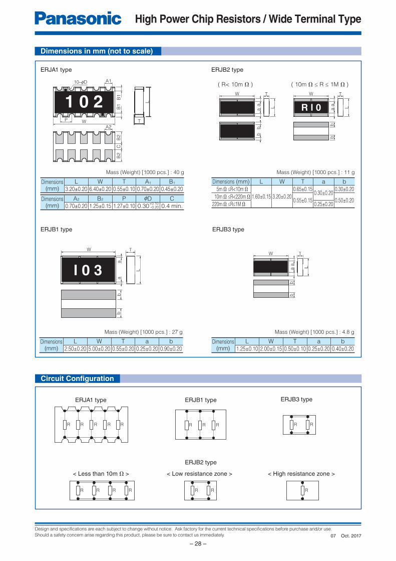
A2
B2
B1
A110–fD
B1
L
B2
CP TW
1 0 2
l 0 3
bb
TW
aa
L
R l 0
bb
TW
aa L
bb
TW
aa L
bb
TW
aa L
R RR RR R RR R R
RR RR R R R
ERJA1 type
Di men sions(mm)
L W T A1 B1
3.20±0.20 6.40±0.20 0.55±0.10 0.70±0.20 0.45±0.20
Di men sions(mm)
A2 B2 P 0D C
0.70±0.20 1.25±0.15 1.27±0.10 0.30+0.10
0.4 min.–0.20
Di men sions(mm)
L W T a b
1.25±0.10 2.00±0.15 0.50±0.10 0.25±0.20 0.40±0.20
ERJB2 type
Mass (Weight) [1000 pcs.] : 11 g
Di men sions(mm)
L W T a b
2.50±0.20 5.00±0.20 0.55±0.20 0.25±0.20 0.90±0.20
ERJB3 type ERJB1 type
Mass (Weight) [1000 pcs.] : 27 g
Mass (Weight) [1000 pcs.] : 40 g
( R< 10m Ω ) ( 10m Ω ≤ R ≤ 1M Ω )
Di men sions (mm) L W T a b
5m Ω ≤R<10m Ω1.60±0.15 3.20±0.20
0.65±0.150.30±0.20
0.30±0.20
10m Ω ≤R<220m Ω0.55±0.15 0.50±0.20
220m Ω ≤R≤1M Ω 0.25±0.20
Mass (Weight) [1000 pcs.] : 4.8 g
Dimensions in mm (not to scale)
ERJA1 type ERJB1 type ERJB3 type
ERJB2 type
< High resistance zone >< Less than 10m Ω > < Low resistance zone >
Circuit Confi guration
Oct. 201707

Design and specifications are each subject to change without notice. Ask factory for the current technical specifications before purchase and/or use.
Should a safety concern arise regarding this product, please be sure to contact us immediately.
High Power Chip Resistors / Wide Terminal Type
– 29 –
Test ItemPerformance
RequirementsTest Conditions
ResistanceWithin Specifi ed
Tolerance20 °C
T. C. R.Within Specifi ed
T. C. R.+25 °C/+125 °C
Overload ±2%
ERJA1, ERJB1 (R > 10), ERJB3 (R > 1) : Rated Voltage × 2.5, 5 s
ERJB2 (R > 10) : Rated Voltage × 2.2, 5 s
ERJB1 (R ≤ 10), ERJB2 (R ≤ 10), ERJB3 (R ≤ 1) : Rated Voltage × 2.0, 5 s
Resistance to Soldering Heat ±1% 270 °C, 10 s
Rapid Change of
Temperature±2% –-55 °C (30min.) / +125 °C (30min.), 1000 cycles
High Temperature
Exposure±1% +155 °C, 1000 h
Damp Heat, Steady State ±1% 60 °C, 90% to 95 %RH, 1000 h
Load Life in Humidity ±3% 60 °C, 90% to 95 %RH, Rated Voltage, 1.5 h ON/0.5 h OFF cycle, 1000 h
Endurance at 70 °C ±3% 70 °C, Rated Voltage, 1.5 h ON/0.5 h OFF cycle, 1000 h
Perfomance
Oct. 201707

Design and specifications are each subject to change without notice. Ask factory for the current technical specifications before purchase and/or use.
Should a safety concern arise regarding this product, please be sure to contact us immediately.
High Precision Thick Film Chip Resistors
– 30 –
E
1
R
2
J
3
P
4
B
5
6
6
B
7
1
8
0
9
0
10
2
11
V
12
Thick FilmChip Resistors
Product Code Size, Power Rating
Code
PB3
PB6
Power R.
0.20 W
0.25 W
Resistance Tolerance
Code
B
D
Tolerance
± 0.1 %
± 0.5 %
The first three digits are significant figures of resistance and the last one denotes number of zeros following. Example : 5110 → 511 Ω : 1003 → 100k Ω
Resistance Value Packaging Methods
Code Part No.
ERJPB3ERJPB6
Packaging
VPunched Carrier Taping4 mm pitch, 5,000 pcs.
Inch
0603
0805
a
b
t
W
L
High Precision Thick Film Chip Resistors
Type: ERJ PB3, PB6
● Achieve the resistance tolerance ±0.1 % with high reliability metal glaze thick fi lm resistor ● Guarantee the temperature coeffi cient of Resistance ±50×10−6/°C in high resistance range up to 1M Ω● Suitable for both refl ow and fl ow soldering● High power … 0.20 W : 0603 inch / 1608 mm size (ERJPB3)
0.25 W : 0805 inch / 2012 mm size (ERJPB6)
● Reference Standards… IEC 60115-8, JIS C 5201-8, EIAJ RC-2134B● AEC-Q200 qualifi ed● RoHS compliant
■ As for Packaging Methods, Land Pattern, Soldering Conditions and Safety Precautions, Please see Data Files
Features
Explanation of Part Numbers
Thick fi lmresistive element
Electrode (Inner)
Electrode (Outer)
Electrode(Between)
Alumina substrate
Protective coating
Part No.(inch size)
Dimensions (mm) Mass (Weight) [g/1000 pcs.]L W a b t
ERJPB3(0603)
1.60±0.15 0.80+0.15 0.15+0.15 0.25±0.10 0.45±0.10 2
ERJPB6(0805)
2.00±0.20 1.25±0.10 0.25±0.20 0.40±0.20 0.60±0.10 4
–0.05 –0.10
Construction Dimensions in mm (not to scale)
Feb. 201600

Design and specifications are each subject to change without notice. Ask factory for the current technical specifications before purchase and/or use.
Should a safety concern arise regarding this product, please be sure to contact us immediately.
High Precision Thick Film Chip Resistors
– 31 –
–60 –40 –20 0 20 40 60 80 100 120 140 160 1800
20
40
60
80
10070 °C
155 °C
Ambient Temperature (°C)
Ra
ted
Lo
ad
(%
) –55 °C
(1) Rated Continuous Working Voltage (RCWV) shall be de ter mined from RCWV=√Power Rating × Re sis tance Values, or Limiting Element Voltage list ed above, whichever less.(2) Overload (Short-time Overload) Test Voltage (SOTV) shall be de termined from SOTV=2.5 × RCWV or max. Over load Volt age list ed above which ev er less.(3) Use it on the condition that the case temperature is below 155 °C.
Power Derating Curve
For resistors operated in ambient temperatures above
70 °C, power rating shall be derated in accordance with
the fi gure on the right.
Ratings
Part No.(inch size)
Power Rating(3)
at 70 °C(W)
LimitingElementVoltage
(1)
(V)
MaximumOverloadVoltage
(2)
(V)
ResistanceTolerance
(%)
ResistanceRange
(Ω)
T.C.R.(×10
–6/°C)
CategoryTemperatureRange (°C)
ERJPB3(0603)
0.20 150 200±0.1±0.5
200 to 100k (E24, E96)
±50 –55 to +155
ERJPB6(0805)
0.25 150 200±0.1±0.5
200 to 1M (E24, E96)
±50 –55 to +155
Feb. 201600

Design and specifications are each subject to change without notice. Ask factory for the current technical specifications before purchase and/or use.
Should a safety concern arise regarding this product, please be sure to contact us immediately.
Anti-Surge Thick Film Chip Resistors
– 32 –
E
1
R
2
J
3
P
4
0
5
6
6
D
7
1
8
0
9
0
10
2
11
V
12
Thick FilmChip Resistors
Product Code Size, Power Rating
Code
PA2
P03
PA3
P06
P08
P14
Power R.
0.20 W
0.20 W
0.25 W
0.50 W
0.66 W
0.50 W
Resistance Tolerance
Code
D
F
J
Tolerance
± 0.5 %
± 1 %
± 5 %
The first two or three digits are significant figures of resistance and the third or 4th one denotes number of zeros following.Three digit type (±5 %), four digit type (±1 %, ±0.5 %) Example: 222→2.2k Ω, 1002→10k Ω
Resistance Value Packaging Methods
Code
V
U
Part No.
ERJP14
ERJPA2
ERJP03ERJPA3ERJP06ERJP08
Packaging
Punched Carrier Taping4 mm pitch, 5,000 pcs.
XPunched Carrier Taping2 mm pitch, 10,000 pcs.
Embossed Carrier Taping4 mm pitch, 5,000 pcs.
Inch
0402
0603
0603
0805
1206
1210
a
b
t
W
L
Anti-Surge Thick Film Chip Re sis tors
Type: ERJ PA2, P03, PA3, P06, P08, P14
● ESD surge characteristics superior to standard metal fi lm resistors● High reliability
Metal glaze thick fi lm resistive element and three layers of electrodes
● Suitable for both refl ow and fl ow soldering● High power … 0.20 W : 0402 inch / 1005 mm size (ERJPA2), 0603 inch / 1608 mm size (ERJP03)
0.25 W : 0603 inch / 1608 mm size (ERJPA3)
0.50 W : 0805 inch / 2012 mm size (ERJP06), 1210 inch / 3225 mm size (ERJP14)
0.66 W : 1206 inch / 3216 mm size (ERJP08)
● Reference Standards… IEC 60115-8, JIS C 5201-8, EIAJ RC-2134B● AEC-Q200 qualifi ed● RoHS compliant
■ As for Packaging Methods, Land Pattern, Soldering Conditions and Safety Precautions, Please see Data Files
Features
Explanation of Part Numbers
Thick fi lmresistive element
Electrode (Inner)
Electrode (Outer)
Electrode(Between)
Alumina substrate
Protective coating
Part No.Dimensions (mm) Mass (Weight)
[g/1000 pcs.]L W a b t
ERJPA2 1.00±0.05 0.50±0.05 0.20±0.15 0.25±0.05 0.35±0.05 0.8
ERJP03 1.60±0.15 0.80+0.15 0.15+0.15 0.30±0.15 0.45±0.10 2
ERJPA3 1.60±0.15 0.80+0.15 0.15+0.15 0.25±0.10 0.45±0.10 2
ERJP06 2.00±0.20 1.25±0.10 0.25±0.20 0.40±0.20 0.60±0.10 4
ERJP08 3.20+0.05
1.60+0.05
0.40±0.20 0.50±0.20 0.60±0.10 10
ERJP14 3.20±0.20 2.50±0.20 0.35±0.20 0.50±0.20 0.60±0.10 16
–0.20 –0.15
–0.05 –0.10
–0.05 –0.10
Construction Dimensions in mm (not to scale)
Nov. 201711
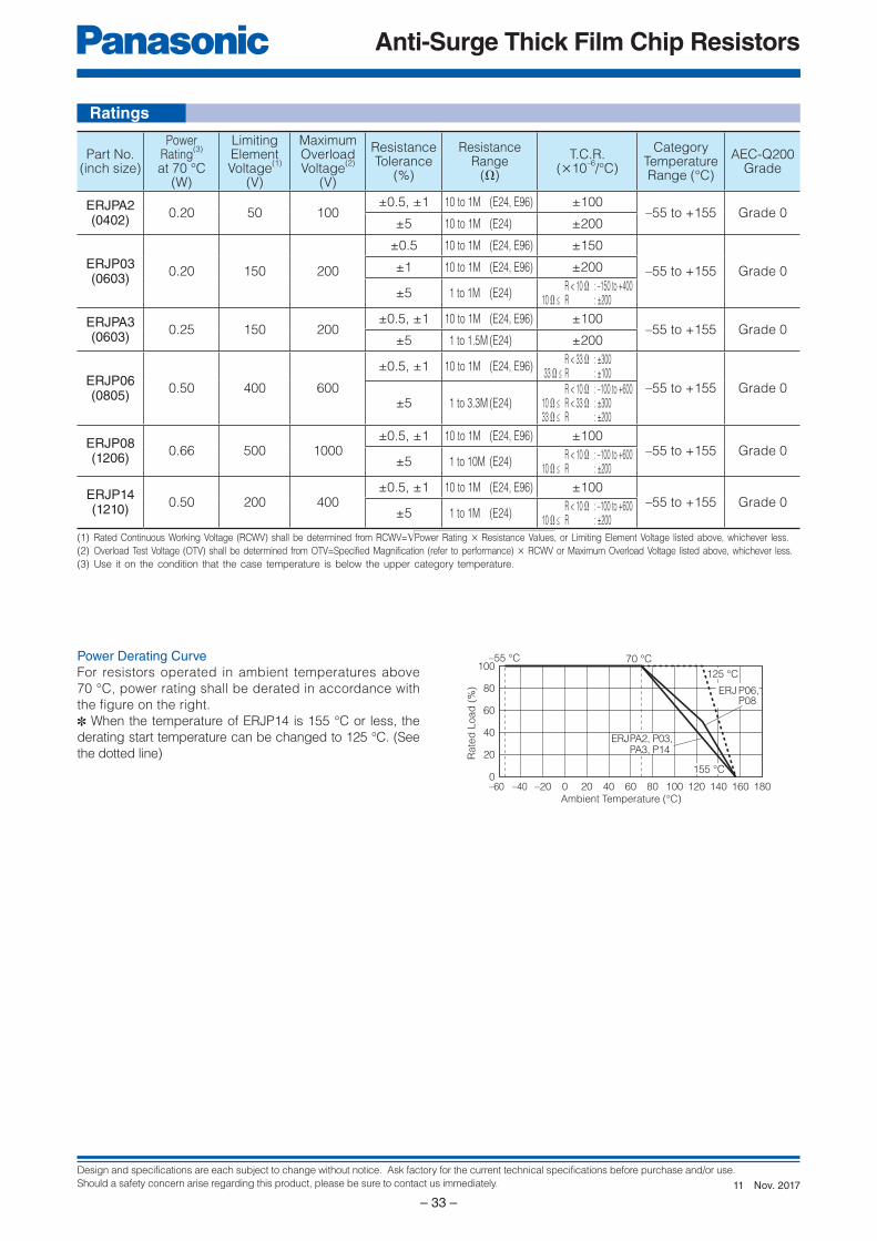
Design and specifications are each subject to change without notice. Ask factory for the current technical specifications before purchase and/or use.
Should a safety concern arise regarding this product, please be sure to contact us immediately.
Anti-Surge Thick Film Chip Resistors
– 33 –
–40 –20 0 20 40 60 80 100 120 140 1600
180–60
70 °C–55 °C
20
40
60
80
100
Rate
d L
oad
(%
)
Ambient Temperature (°C)
155 °C
125 °C
ERJ P06, P08
ERJ PA2, P03, PA3, P14
(1) Rated Continuous Working Voltage (RCWV) shall be de ter mined from RCWV=√Power Rating × Re sis tance Values, or Limiting Element Voltage list ed above, whichever less.
(2) Overload Test Voltage (OTV) shall be determined from OTV=Specified Magnification (refer to performance) × RCWV or Maximum Overload Voltage listed above, whichever less.
(3) Use it on the condition that the case temperature is below the upper category temperature.
Power Derating Curve
For resistors operated in ambient temperatures above
70 °C, power rating shall be derated in accordance with
the fi gure on the right.
✽ When the temperature of ERJP14 is 155 °C or less, the
derating start temperature can be changed to 125 °C. (See
the dotted line)
Ratings
Part No.(inch size)
Power Rating
(3)
at 70 °C(W)
LimitingElementVoltage
(1)
(V)
MaximumOverloadVoltage
(2)
(V)
ResistanceTolerance
(%)
ResistanceRange
(Ω)
T.C.R.(×10
–6/°C)
CategoryTemperatureRange (°C)
AEC-Q200 Grade
ERJPA2(0402)
0.20 50 100±0.5, ±1 10 to 1M (E24, E96) ±100
–55 to +155 Grade 0±5 10 to 1M (E24) ±200
ERJP03(0603)
0.20 150 200
±0.5 10 to 1M (E24, E96) ±150
–55 to +155 Grade 0±1 10 to 1M (E24, E96) ±200
±5 1 to 1M (E24) R < 10 Ω : –150 to +40010 Ω ≤ R : ±200
ERJPA3(0603)
0.25 150 200±0.5, ±1 10 to 1M (E24, E96) ±100
–55 to +155 Grade 0±5 1 to 1.5M (E24) ±200
ERJP06(0805)
0.50 400 600
±0.5, ±1 10 to 1M (E24, E96) R < 33 Ω : ±30033 Ω ≤ R : ±100
–55 to +155 Grade 0±5 1 to 3.3M (E24)
R < 10 Ω : –100 to +60010 Ω ≤ R < 33 Ω : ±30033 Ω ≤ R : ±200
ERJP08(1206)
0.66 500 1000±0.5, ±1 10 to 1M (E24, E96) ±100
–55 to +155 Grade 0±5 1 to 10M (E24)
R < 10 Ω : –100 to +60010 Ω ≤ R : ±200
ERJP14(1210)
0.50 200 400±0.5, ±1 10 to 1M (E24, E96) ±100
–55 to +155 Grade 0±5 1 to 1M (E24)
R < 10 Ω : –100 to +60010 Ω ≤ R : ±200
Nov. 201711
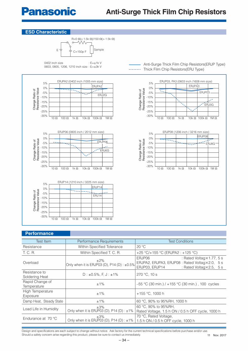
Design and specifications are each subject to change without notice. Ask factory for the current technical specifications before purchase and/or use.
Should a safety concern arise regarding this product, please be sure to contact us immediately.
Anti-Surge Thick Film Chip Resistors
– 34 –
Cha
nge
Rat
io o
fR
esis
tanc
e V
alue
Cha
nge
Rat
io o
fR
esis
tanc
e V
alue
Cha
nge
Rat
io o
fR
esis
tanc
e V
alue
Cha
nge
Rat
io o
fR
esis
tanc
e V
alue
-30%
-25%
-15%
-10%
-5%
0%
5%
-20%
-30%
-25%
-15%
-10%
-5%
0%
5%
-20%
-30%
-25%
-15%
-10%
-5%
0%
5%
-20%
ERJP03, PA3 (0603 inch /1608 mm size)
ERJP08 (1206 inch / 3216 mm size)ERJP06 (0805 inch / 2012 mm size)
ERJP14 (1210 inch / 3225 mm size)
-30%
-25%
-15%
-10%
-5%
0%
5%
-20%
ERJ6G
ERJP06
ERJ3G
ERJP14
ERJ14
ERJP08
ERJ8G
ERJP03
ERJPA3
Cha
nge
Rat
io o
fR
esis
tanc
e V
alue
-30%
-25%
-15%
-10%
-5%
0%
5%
-20%
ERJPA2 (0402 inch /1005 mm size)
ERJ2G
ERJPA2
10 Ω 100 Ω 1k Ω 10k Ω 100k Ω 1M Ω
10 Ω 100 Ω 1k Ω 10k Ω 100k Ω 1M Ω
10 Ω 100 Ω 1k Ω 10k Ω 100k Ω 1M Ω
10 Ω 100 Ω 1k Ω 10k Ω 100k Ω 1M Ω
10 Ω 100 Ω 1k Ω 10k Ω 100k Ω 1M Ω
R=0 Ω(≤ 1.5k Ω)/150 Ω(> 1.5k Ω)
C=150p FSampleE
Anti-Surge Thick Film Chip Resistors(ERJP Type)
Thick Film Chip Resistors(ERJ Type)
ESD Characteristic
0402 inch size : E=±1k V
0603, 0805, 1206, 1210 inch size : E=±3k V
Test Item Performance Requirements Test Conditions
Resistance Within Specifi ed Tolerance 20 °C
T. C. R. Within Specifi ed T. C. R. +25 °C/+155 °C (ERJPA2 : +125 °C)
Overload±2%
Only when it is ERJP03 (D), P14 (D) : ±0.5%
ERJP06 : Rated Voltag×1.77, 5 s
ERJPA2, ERJPA3, ERJP08 : Rated Voltag×2.0, 5 s
ERJP03, ERJP14 : Rated Voltag×2.5, 5 s
Resistance to
Soldering HeatD : ±0.5%, F, J : ±1% 270 °C, 10 s
Rapid Change of
Temperature±1% –55 °C (30 min.) / +155 °C (30 min.) , 100 cycles
High Temperature
Exposure±1% +155 °C, 1000 h
Damp Heat, Steady State ±1% 60 °C, 90% to 95%RH, 1000 h
Load Life in Humidity ±3%Only when it is ERJP03 (D), P14 (D) : ±1%
60 °C, 90% to 95%RH,
Rated Voltage, 1.5 h ON / 0.5 h OFF cycle, 1000 h
Endurance at 70 °C ±3%Only when it is ERJP03 (D), P14 (D) : ±1%
70 °C, Rated Voltage,
1.5 h ON / 0.5 h OFF cycle, 1000 h
Performance
Nov. 201711

Design and specifications are each subject to change without notice. Ask factory for the current technical specifications before purchase and/or use.
Should a safety concern arise regarding this product, please be sure to contact us immediately.
Anti-Pulse Thick Film Chip Resistors
– 35 –
E
1
R
2
J
3
T
4
0
5
6
6
J
7
1
8
0
9
0
10 11
V
Thick FilmChip Resistors
Product Code Size, Power Rating
Code
T06
T08
T14
Power R.
0.25 W
0.33 W
0.5 W
Resistance Tolerance
Code
J
Tolerance
± 5 %
The first two digits are significant figures of resistanceand the third one denotes number of zeros following.
Example: 222→2.2 kΩ
Resistance Value
Packaging Methods
Code
V
U
Part No.
ERJT06ERJT08
ERJT14
Packaging
Punched Carrier Taping4 mm pitch, 5,000 pcs.
Embossed Carrier Taping4 mm pitch, 5,000 pcs.
Inch
0805
1206
1210
E
1
R
2
J
3
T
4
1
5
4
6
M
7
1
8
0
9
0
10 11
U
Thick FilmChip Resistors
Product Code Size, Power Rating
Code
T14
Power R.
0.5 W
Resistance Tolerance
Code
K
M
Tolerance
±10 %
±20 %
Product specifications
Code
L
Specifications
Trimming-less
The first two digits are significant figures of resistance
and the third one denotes number of zeros following.
Example: 222→2.2 kΩ
Resistance Value
Packaging Methods
Code
U
Part No.
ERJT14L
Packaging
Embossed Carrier Taping4 mm pitch, 5,000 pcs.
Inch
1210
L
7
✽ Please contact us for 2012 (mm) and 3216 (mm) size trimming-less types.
Anti-PulseThick Film Chip Re sis tors
Type: ERJ T06, T08, T14 ERJ T14L
Explanation of Part Numbers
Features
● Anti-Pulse characteristics High pulse characteristics achieved by the optimized trimming specifi cations (ERJT06, T08, T14)● Further high pulse characteristics achieved by trimming-less specifi cations (ERJT14L)● High reliability Metal glaze thick fi lm resistive element and three layers of electrodes● Suitable for both refl ow and fl ow soldering● High power … 0.25W : 0805 inch / 2012 mm size (ERJT06) 0.33W : 1206 inch / 3216 mm size (ERJT08) 0.50W : 1210 inch / 3225 mm size (ERJT14, ERJT14L)● Reference Standards…IEC 60115-8, JIS C 5201-8, EIAJ RC-2134B● AEC-Q200 qualifi ed● RoHS compliant
● ERJT06, T08, T14 Type
● ERJT14L Type
■ As for Packaging Methods, Land Pattern, Soldering Conditions and Safety Precautions, Please see Data Files
Nov. 201506

Design and specifications are each subject to change without notice. Ask factory for the current technical specifications before purchase and/or use.
Should a safety concern arise regarding this product, please be sure to contact us immediately.
Anti-Pulse Thick Film Chip Resistors
– 36 –
–40 –20 0 20 40 60 80 100 120 140 1600
180–60
70 °C–55 °C
20
40
60
80
100
Rate
d L
oad
(%
)
Ambient Temperature (°C)
155 °C
a
b
t
W
L
Ratings
(1) Rated Continuous Working Voltage (RCWV) shall be de ter mined from RCWV=√Power Rating × Re sis tance Values, or Limiting Element Voltage list ed above, whichever less.
(2) Overload (Short-time Overload) Test Voltage (SOTV) shall be de termined from SOTV=2.5 × RCWV or max. Over load Volt age list ed above which ev er less.
Part No.(inch size)
Power Ratingat 70 °C
(W)
LimitingElementVoltage
(1)
(V)
MaximumOverloadVoltage
(2)
(V)
ResistanceTolerance
(%)
ResistanceRange
(Ω)
T.C.R.(×10
–6/°C)
CategoryTemperature
Range (°C)
ERJT06(0805)
0.25 150 200 ±51 to 1 M
(E24)
Less than 10 Ω : –100 to +600Less than 33 Ω : ±300More than 33 Ω : ±200
–55 to +155
ERJT08(1206)
0.33 200 400 ±51 to 1 M
(E24)Less than 10 Ω : –100 to +600More than 10 Ω : ±200
–55 to +155
ERJT14(1210)
0.50 200 400 ±51 to 1 M
(E24)Less than 10 Ω : –100 to +600More than 10 Ω : ±200
–55 to +155
ERJT14L(1210)
0.50 200 400±10±20
1 to 1 M(E12)
Less than 10 Ω : –100 to +600More than 10 Ω : ±200
–55 to +155
Power Derating CurveFor resistors operated in ambient temperatures above 70 °C, power rating shall be derated in accordance with the figure on the right.
Thick fi lmresistive element
Electrode (Inner)
Electrode (Outer)
Electrode(Between)
Alumina substrate
Protective coating
Part No.(inch size)
Dimensions (mm) Mass (Weight) [g/1000 pcs.]L W a b t
ERJT06(0805)
2.00±0.20
1.25±0.10
0.25±0.20
0.40±0.20
0.60±0.10
4
ERJT08(1206)
3.20+0.05
1.60+0.05
0.40±0.20
0.50±0.20
0.60±0.10
10
ERJT14ERJT14L(1210)
3.20±0.20
2.50±0.20
0.35±0.20
0.50±0.20
0.60±0.10
16
–0.15–0.20
Construction Dimensions in mm (not to scale)
Nov. 201506

Design and specifications are each subject to change without notice. Ask factory for the current technical specifications before purchase and/or use.
Should a safety concern arise regarding this product, please be sure to contact us immediately.
Anti-Pulse Thick Film Chip Resistors
– 37 –
Pulse duration t (msec)
Lim
iting
Pow
er
: P
p (
W)
Pulse duration t (msec) Pulse duration t (msec)
Lim
iting
Pow
er
: P
p (
W)
Lim
iting
Pow
er
: P
p (
W)
1
10
100
1 10 100 10001
10
100
1 10 100 10001
10
100
1000
1 10 100 1000
✽ Please contact us for 2012 (mm) and 3216 (mm) size trimming-less types.
Period time : 10 s
Pulse duration : t
0
Pp
Limiting
Power
: Anti-Pulse Thick Film Chip Resistors (ERJT14L Type) : Anti-Pulse Thick Film Chip Resistors (ERJT Type) : Thick Film Chip Resistors (ERJ Type)
● In rush pulse Characteristic
● ERJT06 (0805 inch/2012 mm size) ● ERJT08 (1206 inch/3216 mm size) ● ERJT14,ERJT14L (1210 inch/3225 mm size)
Test cycle : 1000 cyclesSpec : Resistance value = within ±5%
Limiting Power Curve
Nov. 201506
Design and specifications are each subject to change without notice. Ask factory for the current technical specifications before purchase and/or use.
Should a safety concern arise regarding this product, please be sure to contact us immediately.
Anti-Sulfurated Thick Film Chip Resistors
– 38 –
E
1
R
2
J
3
S
4
0
5
6
6
F
7
1
8
0
9
0
10
2
11
V
12
Thick Film Chip Resistors
Product Code
Size, Power Rating
InchCode
U01
S02
U02S03
U03S06U06S08U08
0.05 W
0.1 W
0.1 W
0.125 W
0.25 W
0201
0402
0603
0805
1206
1210
1812
2010
2512
Power R.
Resistance Tolerance
Code
D
F
Tolerance
± 0.5 %
± 1 %
Code
J
0
Tolerance
± 5 %
Jumper
The first two or three digits are significant figures ofresistance and the third or 4th one denotes numberof zeros following. Jumper is expressed by R00.Three digit type (±5%), four digit type (±0.5%, ±1%) Example: 222→2.2k Ω, 1002→10k Ω
Resistance Value
Code Inch
S14U14S12
U12S1DU1DS1TU1T
0.5 W
0.75 W
0.75 W
1 W
Power R.
Packaging Methods
Code Packaging Part No.
Pressed Carrier Taping2 mm pitch, 15,000 pcs.
ERJU01
Embossed Carrier Taping4 mm pitch, 4,000 pcs.
Embossed Carrier Taping4 mm pitch, 5,000 pcs.
ERJS1T, ERJU1T
ERJS03, ERJU03ERJS06, ERJU06ERJS08, ERJU08ERJS14, ERJU14ERJS12, ERJU12ERJS1D, ERJU1D
ERJS02, ERJU02
C
Punched Carrier Taping2 mm pitch, 10,000 pcs.X
Punched Carrier Taping4 mm pitch, 5,000 pcs.V
U
6 S J R 2 0 VE
1
R
2
J
3
U
4 5 6 7 8 9 10 11
Code
U6 0.25 W
Power R. Code
S
Q
Resistance Value
0.1 Ω to 0.2 Ω
0.22 Ω to 1 Ω
Resistance Tolerance
Code
F
G
J
Tolerance
±1 %
±2 %
±5 %
Packaging Methods
Code Part No.PackagingShown by 3 digits or letters.
(Example)
R20 : 0.20 Ω=200m Ω 1R0 : 1.0 Ω=1000m Ω
Resistance Value
ERJU6SERJU6Q
Res. Value
Punched Carrier Taping4 mm pitch, 5,000 pcs.V
Thick Film Chip Resistors
Product Code
Size, Power Rating
Inch
0805
Anti-SulfuratedThick Film Chip Resistors
Type: ERJ S02, S03, S06, S08, S14, S12, S1D, S1T (Au-based inner electrode type)Type: ERJ U01, U02, U03, U06, U08, U14, U12, U1D, U1T, U6S, U6Q (Ag-Pd-based inner electrode type)
Explanation of Part Numbers
Features
● High resistance to sulfurization achieved by adopting an Au-based inner electrode (ERJS type) and Ag-Pd-based inner electrode (ERJU type)● High reliability Metal glaze thick fi lm resistive element and three layers of electrodes● Suitable for both refl ow and fl ow soldering● Low Resistance type…ERJU6S, U6Q : 0.1 Ω to 1.0 Ω● Reference Standard…IEC 60115-8, JIS C 5201-8, EIAJ RC-2134B● AEC-Q200 qualifi ed (Exemption ERJU01)● RoHS compliant
■ As for Packaging Methods, Land Pattern, Soldering Conditions and Safety Precautions, Please see Data Files
● ERJU01 to ERJU1T, ERJS02 to ERJS1T Type
● ERJU6S, U6Q Type
Nov. 201710

Design and specifications are each subject to change without notice. Ask factory for the current technical specifications before purchase and/or use.
Should a safety concern arise regarding this product, please be sure to contact us immediately.
Anti-Sulfurated Thick Film Chip Resistors
– 39 –
a
b
t
W
L
Ratings
(1) Rated Continuous Working Voltage (RCWV) shall be de ter mined from RCWV=√Power Rating × Re sis tance Values, or Limiting Element Voltage list ed above, whichever less.
(2) Overload Test Voltage (OTV) shall be determined from OTV=Specified Magnification (refer to performance) × RCWV or Maximum Overload Voltage listed above, whichever less.
(3) Use it on the condition that the case temperature is below the upper category temperature.
(1) Use it on the condition that the case temperature is below the upper category temperature.
· Rated Continuous Working Voltage (RCWV) shall be determined from RCWV = Power Rating × Resistance Values.
· Overload Test Voltage (OTV) shall be determined from OTV = Specified Magnification (refer to performance) × RCWV.
Part No.(inch size)
PowerRating (3)
at 70 °C(W)
LimitingElementVoltage(1)
(V)
MaximumOverloadVoltage(2)
(V)
ResistanceTolerance
(%)
ResistanceRange
(Ω)
T.C.R.(×10
-6/°C )
CategoryTemperature
Range(°C)
AEC-Q200 Grade
ERJU01(0201) 0.05 25 50
±1 10 to 1M (E24, E96)
<10 Ω:–100 to +600
10 Ω to 1M Ω:±200(±5%)±100(±0.5, ±1%)✽
✽ ERJU01,ERJS02,ERJU02 : ±200
1M Ω<:–400 to +150
–55 to +125 –±5 1 to 1M (E24)
ERJS02ERJU02(0402)
0.1 50 100±0.5, ±1 1 to 1M (E24, E96)
–55 to +155 Grade 0±5 1 to 3.3M (E24)
ERJS03ERJU03(0603)
0.1 75 150±0.5, ±1 1 to 1M (E24, E96)
–55 to +155 Grade 0±5 1 to 10M (E24)
ERJS06ERJU06(0805)
0.125 150 200±0.5, ±1 1 to 1M (E24, E96)
–55 to +155 Grade 0±5 1 to 10M (E24)
ERJS08ERJU08(1206)
0.25 200 400±0.5, ±1 1 to 1M (E24, E96)
–55 to +155 Grade 0±5 1 to 10M (E24)
ERJS14ERJU14(1210)
0.5 200 400±0.5, ±1 1 to 1M (E24, E96)
–55 to +155 Grade 0±5 1 to 10M (E24)
ERJS12ERJU12(1812)
0.75 200 500±0.5, ±1 1 to 1M (E24, E96)
–55 to +155 Grade 0±5 1 to 10M (E24)
ERJS1DERJU1D(2010)
0.75 200 500±0.5, ±1 1 to 1M (E24, E96)
–55 to +155 Grade 0±5 1 to 10M (E24)
ERJS1TERJU1T(2512)
1.0 200 500±0.5, ±1 1 to 1M (E24, E96)
–55 to +155 Grade 0±5 1 to 10M (E24)
Thick fi lmresistive element
Electrode (Inner)Au-based :ERJS type
Ag-Pd-based:ERJU type
Electrode (Outer)
Electrode(Between)
Alumina substrate
Protective coating
Part No.Dimensions (mm) Mass (Weight)
[g/1000 pcs.]L W a b t
ERJU01 0.60±0.03
0.30±0.03
0.10±0.05
0.15±0.05
0.23±0.03
0.15
ERJS02ERJU02
1.00±0.05
0.50±0.05
0.20±0.10
0.25±0.10
0.35±0.05
0.8
ERJS03ERJU03
1.60±0.15
0.80+0.15
0.30±0.20
0.30±0.15
0.45±0.10
2
ERJS06ERJU06
2.00±0.20
1.25±0.10
0.40±0.20
0.40±0.20
0.60±0.10
4
ERJU6□ 2.00±0.20
1.25±0.10
0.45±0.20
0.45±0.20
0.55±0.10
6
ERJS08 ERJU08
3.20+0.05
1.60+0.05
0.50±0.20
0.50±0.20
0.60±0.10
10
ERJS14ERJU14
3.20±0.20
2.50±0.20
0.50±0.20
0.50±0.20
0.60±0.10
16
ERJS12ERJU12
4.50±0.20
3.20±0.20
0.50±0.20
0.50±0.20
0.60±0.10
27
ERJS1DERJU1D
5.00±0.20
2.50±0.20
0.60±0.20
0.60±0.20
0.60±0.10
27
ERJS1TERJU1T
6.40±0.20
3.20±0.20
0.65±0.20
0.60±0.20
0.60±0.10
45
–0.05
–0.15–0.20
[Low Resistance type]
Part No.(inch size)
PowerRating(1)
at 70 °C(W)
ResistanceTolerance
(%)
ResistanceRange
(Ω)
T.C.R.
(×10-6/°C )
CategoryTemperature
Range(°C)
AEC-Q200 Grade
ERJU6S (0805)0.25 ±1, ±2, ±5
0.1 to 0.2 (E24)±150 –55 to +155 Grade 0
ERJU6Q (0805) 0.22 to 1 (E24)
Construction Dimensions in mm (not to scale)
√
Nov. 201710

Design and specifications are each subject to change without notice. Ask factory for the current technical specifications before purchase and/or use.
Should a safety concern arise regarding this product, please be sure to contact us immediately.
Anti-Sulfurated Thick Film Chip Resistors
– 40 –
–40 –20 0 20 40 60 80 100 120 140 1600
180–60
70 °C
Ambient Temperature (°C)
20
40
60
80
100
Ra
ted
Lo
ad
(%
)
–55 °C
125 °C
ERJU01
155 °C
[For Jumper]
Part No.(inch size)
Rated Current(A)
Maximum Overload Current (1)
(A)
ERJU01(0201) 0.5 1
ERJS02ERJU02(0402)
1 2ERJS03ERJU03(0603)
ERJS06ERJU06(0805)
2 4
ERJS08ERJU08(1206)
ERJS14ERJU14(1210)
ERJS12ERJU12(1812)
ERJS1DERJU1D(2012)
ERJS1TERJU1T(2512)
Power Derating CurveFor resistors operated in ambient temperatures above 70 °C, power rating shall be derated in accordance with the figure below.
Test ItemPerformance Requirements
Test ConditionsResistor type Jumper type
ResistanceWithin Specifi ed
Tolerance100m Ω or less 20 °C
T. C. R.Within Specifi ed
T. C. R.200m Ω or less +25 °C/+155 °C (ERJU01 : +25 °C/+125 °C)
Overload ±2% 100m Ω or lessRated Voltage × 2.5, 5sJumper type : Max. Overload Current, 5 s
Resistance to Soldering Heat
±1% 100m Ω or less 270 °C, 10 s
Rapid Change of Temperature
±1% 100m Ω or less–55 °C (30min.) / +155 °C (ERJU01: +125 °C) (30min.), 100 cycles
High Temperature Exposure
±1% 100m Ω or less +155 °C (ERJU01 : +125 °C), 1000 h
Damp Heat, Steady State ±1% 100m Ω or less 60 °C, 90% to 95 %RH, 1000 h
Load Life in Humidity ±3% 100m Ω or less60 °C, 90% to 95 %RH, Rated Voltage (Jumper type : Rated Current), 1.5 h ON/0.5 h OFF cycle, 1000h
Endurance at 70 °C ±3% 100m Ω or less70 °C, Rated Voltage (Jumper type : Rated Current), 1.5 h ON/0.5 h OFF cycle, 1000 h
Test ItemPerformance Requirements
Test Conditions
ResistanceWithin Specifi ed
Tolerance20 °C
T. C. R.Within Specifi ed
T. C. R.+25 °C/+125 °C
Overload ±1% Rated Voltage × 2.5, 5 s
Resistance to Soldering Heat ±1% 270 °C, 10 s
Rapid Change of Temperature ±1% –55 °C (30min.) / +125 °C (30min.), 100 cycles
High Temperature Exposure ±1% +155 °C, 1000 h
Damp Heat, Steady State ±1% 60 °C, 90% to 95%RH, 1000 h
Load Life in Humidity ±3%60 °C, 90% to 95%RH, Rated Voltage, 1.5 h ON/0.5 h OFF cycle, 1000 h
Endurance at 70 °C ±3% 70 °C, Rated Voltage, 1.5 h ON/0.5 h OFF cycle, 1000 h
● ERJU01 to ERJU1T, ERJS02 to ERJS1T Type
● ERJU6S, U6Q Type
Performance
(1) Overload test current
Nov. 201710
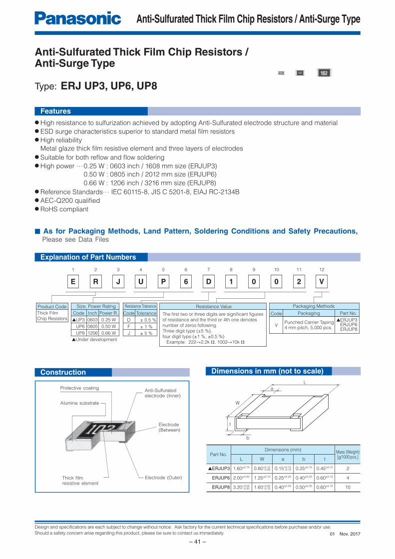
Design and specifications are each subject to change without notice. Ask factory for the current technical specifications before purchase and/or use.
Should a safety concern arise regarding this product, please be sure to contact us immediately.
Anti-Sulfurated Thick Film Chip Resistors / Anti-Surge Type
– 41 –
a
b
t
W
L
E
1
R
2
J
3
U
4
P
5
6
6
D
7
1
8
0
9
0
10
2
11
V
12
Thick FilmChip Resistors
Product Code Size, Power Rating
Code
▲UP3
UP6
UP8
▲Under development
Power R.
0.25 W
0.50 W
0.66 W
Resistance Tolerance
Code
D
F
J
Tolerance
± 0.5 %
± 1 %
± 5 %
The first two or three digits are significant figures of resistance and the third or 4th one denotes number of zeros following.Three digit type (±5 %), four digit type (±1 %, ±0.5 %)
Example: 222→2.2k Ω, 1002→10k Ω
Resistance Value Packaging Methods
Code Part No.
▲ERJUP3ERJUP6ERJUP8
Packaging
VPunched Carrier Taping4 mm pitch, 5,000 pcs.
Inch
0603
0805
1206
Thick fi lmresistive element
Anti-Sulfurated electrode (Inner)
Electrode (Outer)
Electrode(Between)
Alumina substrate
Protective coating
Anti-Sulfurated Thick Film Chip Resistors / Anti-Surge Type
Type: ERJ UP3, UP6, UP8
● High resistance to sulfurization achieved by adopting Anti-Sulfurated electrode structure and material● ESD surge characteristics superior to standard metal fi lm resistors● High reliability
Metal glaze thick fi lm resistive element and three layers of electrodes
● Suitable for both refl ow and fl ow soldering● High power … 0.25 W : 0603 inch / 1608 mm size (ERJUP3) 0.50 W : 0805 inch / 2012 mm size (ERJUP6) 0.66 W : 1206 inch / 3216 mm size (ERJUP8)
● Reference Standards… IEC 60115-8, JIS C 5201-8, EIAJ RC-2134B● AEC-Q200 qualifi ed● RoHS compliant
■ As for Packaging Methods, Land Pattern, Soldering Conditions and Safety Precautions, Please see Data Files
Features
Construction Dimensions in mm (not to scale)
Explanation of Part Numbers
Part No.Dimensions (mm) Mass (Weight)
[g/1000 pcs.]L W a b t
▲ERJUP3 1.60±0.15 0.80+0.15 0.15+0.15 0.25±0.10 0.45±0.10 2
ERJUP6 2.00±0.20 1.25±0.10 0.25±0.20 0.40±0.20 0.60±0.10 4
ERJUP8 3.20+0.05 1.60+0.05 0.40±0.20 0.50±0.20 0.60±0.10 10–0.20 –0.15
–0.05 –0.10
Nov. 201701

Design and specifications are each subject to change without notice. Ask factory for the current technical specifications before purchase and/or use.
Should a safety concern arise regarding this product, please be sure to contact us immediately.
Anti-Sulfurated Thick Film Chip Resistors / Anti-Surge Type
– 42 –
–60 –40 –20 0 20 40 60 80 100 120 140 160 1800
20
40
60
80
100
155 °C
Ambient Temperature (°C)
Rate
d L
oa
d (
%) –55 °C 70 °C
125 °C50 %
ERJUP6, UP8
ERJUP3
10 Ω-30%
-25%
-15%
Cha
nge
Rat
io o
fR
esis
tanc
e V
alue
-10%
-5%
0%
5%
-20%
100 Ω 1k Ω 10k Ω 100k Ω 1M Ω
ERJUP8 (1206 inch / 3216 mm size)
ERJUP8
ERJU08
Cha
nge
Rat
io o
fR
esis
tanc
e V
alue
Cha
nge
Rat
io o
fR
esis
tanc
e V
alue
10 Ω-30%
-25%
-15%
-10%
-5%
0%
5%
-20%
100 Ω
▲ERJUP3 (0603 inch / 1608 mm size)
1k Ω 10k Ω 100k Ω 1M Ω
ERJU03
ERJUP3
ERJUP6 (0805 inch / 2012 mm size)
10 Ω-30%
-25%
-15%
-10%
-5%
0%
5%
-20%
100 Ω 1k Ω 10k Ω 100k Ω 1M Ω
ERJU06
ERJUP6
(1) Rated Continuous Working Voltage (RCWV) shall be de ter mined from RCWV=√Power Rating × Re sis tance Values, or Limiting Element Voltage list ed above, whichever less.
(2) Overload Test Voltage (OTV) shall be determined from OTV=Specified Magnification (refer to performance) × RCWV or Maximum Overload Voltage listed above, whichever less.
(3) Use it on the condition that the case temperature is below the upper category temperature.
Power Derating Curve
For resistors operated in ambient temperatures above
70 °C, power rating shall be derated in accordance with
the fi gure on the right.
Anti-Sulfurated Thick Film Chip Resistors / Anti-Surge Type (ERJUP Type)
Anti-Sulfurated Thick Film Chip Resistors (ERJU Type)E=±3k V
Ratings
R=0 Ω(≤ 1.5k Ω)/150 Ω(> 1.5k Ω)
C=150p FSampleE
ESD Characteristic
Part No.(inch size)
Power Rating
(3)
at 70 °C(W)
LimitingElementVoltage
(1)
(V)
MaximumOverloadVoltage
(2)
(V)
ResistanceTolerance
(%)
ResistanceRange
(Ω)
T.C.R.(×10
–6/°C)
CategoryTemperatureRange (°C)
AEC-Q200
Grade
▲ERJUP3
(0603)0.25 150 200
±0.5, ±1 10 to 1M (E24, E96) ±100–55 to +155 Grade 0
±5 1 to 1.5M (E24) ±200
ERJUP6
(0805)0.50 400 600
±0.5, ±1 10 to 1M (E24, E96) ±100
–55 to +155 Grade 0±5 1 to 3.3M (E24)
R < 10 Ω : –100 to +600
10 Ω ≤ R : ±200
ERJUP8
(1206)0.66 500 1000
±0.5, ±1 10 to 1M (E24, E96) ±100
–55 to +155 Grade 0±5 1 to 10M (E24)
R < 10 Ω : –100 to +600
10 Ω ≤ R : ±200
Nov. 201701

Design and specifications are each subject to change without notice. Ask factory for the current technical specifications before purchase and/or use.
Should a safety concern arise regarding this product, please be sure to contact us immediately.
Anti-Sulfurated Thick Film Chip Resistors / Anti-Surge Type
– 43 –
Test Item Performance Requirements Test Conditions
Resistance Within Specifi ed Tolerance 20 °C
T. C. R. Within Specifi ed T. C. R. +25 °C/+155 °C
Overload ±2%ERJUP6 : Rated Voltage × 1.77, 5 s
▲ERJUP3, ERJUP8 : Rated Voltage × 2.0, 5 s
Resistance to Soldering Heat D :±0.5%F, J :±1% 270 °C, 10 s
Rapid Change of
Temperature±1% –55 °C (30 min.) / +155 °C (30 min.), 100 cycles
High Temperature Exposure ±1% +155 °C, 1000 h
Damp Heat, Steady State ±1% 60 °C, 90% to 95%RH, 1000 h
Load Life in Humidity ±3%60 °C, 90% to 95%RH,
Rated Voltage, 1.5 h ON / 0.5 h OFF cycle, 1000 h
Endurance at 70 °C ±3% 70 °C, Rated Voltage, 1.5 h ON / 0.5 h OFF cycle, 1000 h
Performance
Nov. 201701
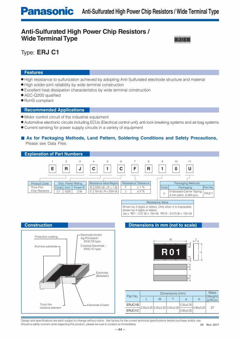
Design and specifications are each subject to change without notice. Ask factory for the current technical specifications before purchase and/or use.
Should a safety concern arise regarding this product, please be sure to contact us immediately.
Anti-Sulfurated High Power Chip Resistors / Wide Terminal Type
– 44 –
R 0 1
bb
TW
aa
L
1 2 3 4 5 6 7 8 9 10 11
Thick FilmChip Resistors
Product Code Size, Power Rating
Code
C1
Resistance Value Region
B
C
Resistance Value
Packaging Methods
U
Code Packaging Part No.
Embossed Carrier Taping
4 mm pitch, 5,000 pcs.
220m Ω ≤ R ≤ 1 Ω
10m Ω ≤ R < 220m Ω
Resistance Tolerance
F
J
± 1 %
± 5 %
Shown by 3 digits or letters. Only when it is impossible, shown by 4 digits or letters.
Power R.
2 WERJC1
(ex.) R01 : 0.01 Ω = 10m Ω R015 : 0.015 Ω = 15m Ω
E R J C 1 F R 1 0 UC
Inch
1020
Anti-Sulfurated High Power Chip Resistors / Wide Terminal Type
Type: ERJ C1
Explanation of Part Numbers
Features
Recommended Applications
● High resistance to sulfurization achieved by adopting Anti-Sulfurated electrode structure and material● High solder-joint reliability by wide terminal con struc tion● Excellent heat dissipation characteristics by wide terminal construction● AEC-Q200 qualifi ed● RoHS compliant
● Motor control circuit of the industrial equipment● Automotive electronic circuits including ECUs (Electrical control unit), anti-lock breaking systems and air-bag systems● Current sensing for power supply circuits in a variety of equipment
■ As for Packaging Methods, Land Pattern, Soldering Conditions and Safety Precautions, Please see Data Files
Part No.Di men sions (mm) Mass
(Weight)[g/1000 pcs.]L W T a b
ERJC1B2.50±0.20 5.00±0.20 0.55±0.20
0.35±0.200.90±0.20 27
ERJC1C 0.60±0.20
Alumina substrate
Thick fi lmresistive element
Electrode (Inner)Ag-Pd-based : ERJC1B type
Covered Electrode : ERJC1C type
Electrode (Outer)
Electrode(Between)
Protective coating
Construction Dimensions in mm (not to scale)
Nov. 201705

Design and specifications are each subject to change without notice. Ask factory for the current technical specifications before purchase and/or use.
Should a safety concern arise regarding this product, please be sure to contact us immediately.
Anti-Sulfurated High Power Chip Resistors / Wide Terminal Type
– 45 –
R RR
–60 –40 –20 0 20 40 60 80 100 120 140 160 1800
20
40
60
80
10070 °C
155 °C
Ambient Temperature (°C)
Rate
d L
oad
(%
) –55 °C
Ratings
Circuit Confi guration
Power Derating CurveFor resistors operated in ambient temperatures above 70 °C, power rating shall be derated in accordance with the figure on the right.
Type ERJC1
Part No.(inch size)
Power Ratingat 70 °C
(1)
(W)
ResistanceTolerance (%)
ResistanceRange
(Ω)
T.C.R.(×10
-6/°C )
CategoryTemperature
Range(°C)
AEC-Q200Grade
ERJC1(1020)
2
±1
10m to 1 (E24)
10m Ω ≤ R < 22m Ω : ±35022m Ω ≤ R < 47m Ω : ±20047m Ω ≤ R < 100m Ω : ±150100m Ω ≤ R ≤ 1 Ω : ±100
–55 to +155 Grade 0
±510m Ω ≤ R < 22m Ω : ±35022m Ω ≤ R < 1 Ω : ±200
(1) Use it on the condition that the case temperature is below the upper category temperature. · Rated Continuous Working Voltage (RCWV) shall be determined from RCWV = Power Rating × Resistance Values. · Overload Test Voltage (OTV) shall be determined from OTV = Specified Magnification (refer to performance) × RCWV.
√
Test ItemPerformance
RequirementsTest Conditions
ResistanceWithin Specifi ed
Tolerance20 °C
T. C. R.Within Specifi ed
T. C. R.+25 °C/+125 °C
Overload ±2% Rated Voltage × 2.0, 5 s
Resistance to Soldering Heat ±1% 270 °C, 10 s
Rapid Change of
Temperature±2% –55 °C (30min.) / +125 °C (30min.), 1000 cycles
High Temperature
Exposure±1% +155 °C, 1000 h
Damp Heat, Steady State ±1% 60 °C, 90% to 95 %RH, 1000 h
Load Life in Humidity ±3%60 °C, 90% to 95 %RH, Rated Voltage,
1.5 h ON/0.5 h OFF cycle, 1000 h
Endurance at 70 °C ±3% 70 °C, Rated Voltage, 1.5 h ON/0.5 h OFF cycle, 1000 h
Perfomance
Nov. 201705

Design and specifications are each subject to change without notice. Ask factory for the current technical specifications before purchase and/or use.
Should a safety concern arise regarding this product, please be sure to contact us immediately.
Chip Resistor Array
– 46 –
E
1
X
2
B
3
V
4
8
5
V
6
4
7
7
8
2
9
J
10
V
11
Thick FilmChip Resistor Networks
Product Code Schematics
VIsolatedtype
The first two digits aresignificant figures ofresistance value andthe third one denotesthe number of zeros
following. Jumper is
expressed by R00
Resistance Value
Example : 222 → 2.2k Ω
ResistanceTolerance
J
0
±5 %
Jumper
Packaging Methods
Code
Nil
X
V
Packaging Part No.
Embossed Carrier Taping4 mm pitch, 2,500 pcs.
Punched Carrier Taping2 mm pitch, 10,000 pcs.
Punched Carrier Taping4 mm pitch, 5,000 pcs.
EXBS8V
EXB14V, 18V,24V, 28V, N8V
EXB2HV, 34V, 38V, V4V, V8V
0201×2
0201×4
0402×2
0402×4
0602×8
0603×2
0603×4
0402×4
0603×2
0603×4
0805×4
14
18
24
28
2H
34
38
N8
V4
V8
S8
Convex Terminal
Flat Terminal
Convex Terminal
Convex Terminal
Convex Terminal
Convex Terminal
Convex Terminal
Concave Terminal
Concave Terminal
Concave Terminal
Concave Terminal
Code ConstructionInch
4
1
3
2
8
1
7
2
6
3
5
4
16
1
15
2
14
3
13
4
12
5
11
6
10
7
9
8
Protective coating
Thick filmresistive element
Electrode (Inner)
Electrode (Between)
Electrode (Outer)
Alumina substrate
Chip Resistor Array
Type: EXB 14V, 18V, 24V, 28V, N8V, 2HV, 34V, V4V, 38V, V8V, S8V
■ As for Packaging Methods, Land Pattern, Soldering Conditions and Safety Precautions, Please see Data Files
● Isolated type
● High density 2 resistors in 0.8 mm × 0.6 mm size / 0302 inch size : EXB14V 4 resistors in 1.4 mm × 0.6 mm size / 0502 inch size : EXB18V 2 resistors in 1.0 mm × 1.0 mm size / 0404 inch size : EXB24V 4 resistors in 2.0 mm × 1.0 mm size / 0804 inch size : EXB28V, EXBN8V 8 resistors in 3.8 mm × 1.6 mm size / 1506 inch size : EXB2HV 2 resistors in 1.6 mm × 1.6 mm size / 0606 inch size : EXB34V, EXBV4V 4 resistors in 3.2 mm × 1.6 mm size / 1206 inch size : EXB38V, EXBV8V 4 resistors in 5.1 mm × 2.2 mm size / 2009 inch size : EXBS8V● Improvement of placement effi ciency Placement effi ciency of Chip Resistor Array is two, four or eight times of the fl at type chip resistor● Reference Standard…IEC 60115-9, JIS C 5201-9, EIAJ RC-2129● AEC-Q200 qualifi ed (EXB2, EXB3)● RoHS compliant
14V, 24V,
34V, V4V
18V, 28V, N8V,
38V, V8V, S8V
2HV
2 resistors 4 resistors 8 resistors
SchematicsConstruction (Example : Concave Terminal)
Features
Explanation of Part Numbers
Feb. 201805

Design and specifications are each subject to change without notice. Ask factory for the current technical specifications before purchase and/or use.
Should a safety concern arise regarding this product, please be sure to contact us immediately.
Chip Resistor Array
– 47 –
–60 –40 –20 0 20 40 60 80 100 120 140 160 1800
20
40
60
80
10070 °C–55 °C
125 °C
Ambient Temperature (°C)
Rate
d L
oad
(%
)
Part No.
(inch size)
Power Rating
at 70 °C
(W / element)
Limiting Element
Voltage (1)
(V)
Maximum Overload
Voltage (2)
(V)
Resistance
Tolerance
(%)
Resistance
Range
(Ω)
T.C.R.
(×10–6
/°C)
Category
Temperature Range
(°C)
AEC-Q200
Grade
EXB14V(0201×2)
0.031 12.5 25 ±5 10 to 1M (E24)
<10 Ω :–200 to +600
10 Ω to1M Ω :±200
–55 to +125 –
EXB18V(0201×2)
0.031
(0.1 W / package)12.5 25 ±5 10 to 1M (E24) –55 to +125 –
EXB24V(0402×2)
0.063 50 100 ±5 1 to 1M (E24) –55 to +125 Grade 1
EXB28V(0402×4)
0.063 50 100 ±5 1 to 1M (E24) –55 to +125 Grade 1
EXB2HV(0602×8)
0.063
(0.25 W / package)25 50 ±5 10 to 1M (E24) –55 to +125 Grade 1
EXB34V(0603×2)
0.063 50 100 ±5 1 to 1M (E24) –55 to +125 Grade 1
EXB38V(0603×4)
0.063 50 100 ±5 1 to 1M (E24) –55 to +125 Grade 1
EXBN8V(0402×4)
0.031 50 100 ±5 10 to 1M (E24) –55 to +125 –
EXBV4V(0603×2)
0.063 50 100 ±5 10 to 1M (E24) –55 to +125 –
EXBV8V(0603×4)
0.063 50 100 ±5 10 to 1M (E24) –55 to +125 –
EXBS8V(0805×4)
0.1 100 200 ±5 10 to 1M (E24) –55 to +125 –
Ratings
Part No.(inch size)
Rated Current(A / element)
Maximum Over load Current (1)
(A)
EXB14V(0201×2)
0.5 1
EXB18V(0201×4)
0.5 1
EXB24V(0402×2)
1 2
EXB28V(0402×4)
1 2
EXB2HV(0602×8)
1 2
EXB34V(0603×2)
1 2
EXB38V(0603×4)
1 2
EXBN8V(0402×4)
1 2
EXBV4V(0603×2)
1 2
EXBV8V(0603×4)
1 2
EXBS8V(0805×4)
2 4
Power Derating CurveFor resistors operated in ambient temperatures above 70 °C, power rating shall be derated in accordance with the figure below.
(1) Overload test current
(1) Rated Continuous Working Voltage (RCWV) shall be de ter mined from RCWV=√Power Rating × Re sis tance Values, or Limiting Element Voltage list ed above, whichever less.
(2) Overload Test Voltage (OTV) shall be determined from OTV=Specified Magnification (refer to performance) × RCWV or Maximum Overload Voltage listed above, whichever less.
[For Jumper]
[For Resistor]
Feb. 201805

Design and specifications are each subject to change without notice. Ask factory for the current technical specifications before purchase and/or use.
Should a safety concern arise regarding this product, please be sure to contact us immediately.
Chip Resistor Array
– 48 –
P PL L
GG G
W
GBB
W
BB
A1 A1 A2EXBV4V EXBN8V, V8V, S8V
T T
PL
T
G
W
GBB
A1 A2 EXB18V
A1
P T P
L
TL
BB
G BB
GG
WW
G
A1 A2EXB14V, 24V, 34V EXB28V, 38V
PTL
G
W
G
BB
A1 A2 EXB2HV
Part No.(inch size)
Dimensions (mm) Mass (Weight)[g/1000 pcs.]L W T A1 A2 B P G
EXBN8V (0402×4) 2.00 ±0.10
1.00±0.10
0.45±0.10
0.30 ±0.10
0.30 ±0.10
0.20±0.15
(0.50) 0.30±0.15
3.0
EXBV4V (0603×2) 1.60+0.20
1.60+0.20
0.60±0.10
0.60 ±0.10
— 0.30±0.15
(0.80) 0.45±0.15
5.0
EXBV8V (0603×4) 3.20+0.20
1.60+0.20
0.60±0.10
0.60 ±0.10
0.60 ±0.10
0.30±0.15
(0.80) 0.45±0.15
10
EXBS8V (0805×4) 5.08+0.20
2.20+0.20
0.70±0.20
0.80±0.15
0.80±0.15
0.50±0.15
(1.27) 0.55±0.15
30
Part No.(inch size)
Dimensions (mm) Mass (Weight)[g/1000 pcs.]L W T A1 A2 B P G
EXB14V (0201×2) 0.80 ±0.10
0.60±0.10
0.35±0.10
0.35±0.10
— 0.15±0.10
(0.50) 0.15±0.10
0.5
EXB24V (0402×2) 1.00±0.10
1.00±0.10
0.35±0.10
0.40±0.10
— 0.18±0.10
(0.65) 0.25±0.10
1.2
EXB28V (0402×4) 2.00±0.10
1.00±0.10
0.35±0.10
0.45±0.10
0.35±0.10
0.20±0.10
(0.50) 0.25±0.10
2.0
EXB2HV (0602×8) 3.80±0.10
1.60±0.10
0.45±0.10
0.35±0.10
0.35±0.10
0.30±0.10
(0.50) 0.30±0.10
9.0
EXB34V (0603×2) 1.60±0.20
1.60±0.15
0.50±0.10
0.65±0.15
— 0.30±0.20
(0.80) 0.30±0.20
3.5
EXB38V (0603×4) 3.20±0.20
1.60±0.15
0.50±0.10
0.65±0.15
0.45±0.15
0.30±0.20
(0.80) 0.35±0.20
7.0
–0.10
–0.10
–0.10
–0.10
–0.10
–0.10
Part No.(inch size)
Dimensions (mm) Mass (Weight)[g/1000 pcs.]L W T A1 A2 B P G
EXB18V (0201×4) 1.40±0.10 0.60±0.10 0.35±0.10 0.20±0.10 0.20±0.10 0.10±0.10 (0.40) 0.20±0.10 1.0
( ) Reference
(1) Convex Terminal type
(2) Concave Terminal type
(3) Flat Terminal type
( ) Reference
( ) Reference
Dimensions in mm (not to scale)
Feb. 201805

Design and specifications are each subject to change without notice. Ask factory for the current technical specifications before purchase and/or use.
Should a safety concern arise regarding this product, please be sure to contact us immediately.
Chip Resistor Array
– 49 –
Test ItemPerformance
RequirementsTest Conditions
ResistanceWithin Specifi ed
Tolerance20 °C
T. C. R.Within Specifi ed
T. C. R.+25 °C/+125 °C
Overload ±2%Rated Voltage × 2.5, 5 s
Jumper type : Max. Overload Current, 5 s
Resistance to Soldering Heat ±1% 270 °C, 10 s
Rapid Change of Temperature ±1% –55 °C (30min.) / +125 °C (30min.), 100 cycles
High Temperature Exposure ±1% +125 °C , 1000 h
Damp Heat, Steady State ±1% 60 °C, 90% to 95 %RH, 1000 h
Load Life in Humidity ±3%60 °C, 90% to 95 %RH, Rated Voltage (Jumper type: Rated Current),
1.5 h ON/0.5 h OFF cycle, 1000 h
Endurance at 70 °C ±3%70 °C, Rated Voltage(Jumper type: Rated Current),
1.5 h ON/0.5 h OFF cycle, 1000 h
Perfomance
Feb. 201805
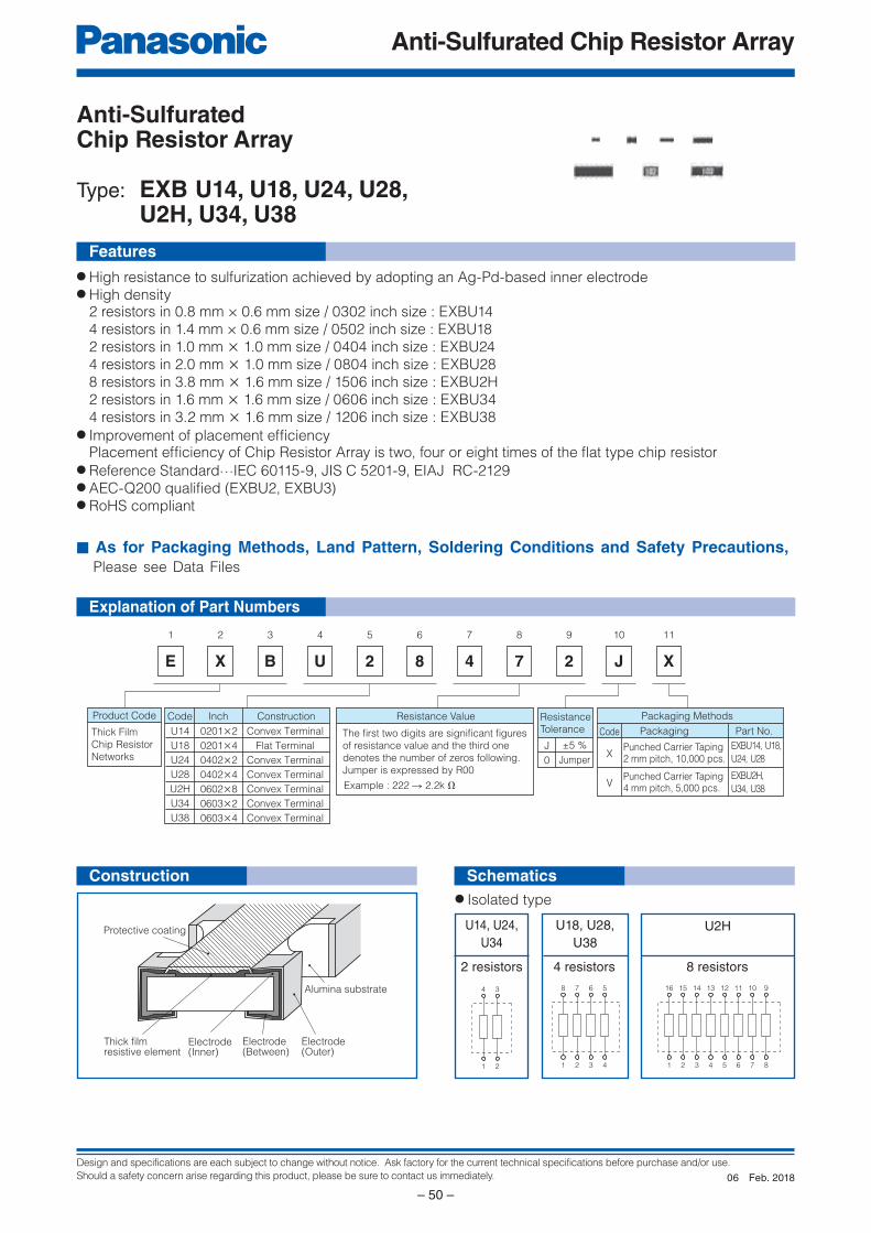
Design and specifications are each subject to change without notice. Ask factory for the current technical specifications before purchase and/or use.
Should a safety concern arise regarding this product, please be sure to contact us immediately.
Anti-Sulfurated Chip Resistor Array
– 50 –
E
1
X
2
B
3
U
4
2
5
8
6
4
7
7
8
2
9
J
10
X
11
Thick FilmChip Resistor Networks
Product Code
The first two digits are significant figures of resistance value and the third one
denotes the number of zeros following. Jumper is expressed by R00
Resistance Value
Example : 222 → 2.2k Ω
ResistanceTolerance
J
0
±5 %
Jumper
Packaging Methods
Code
X
V
Packaging Part No.
Punched Carrier Taping2 mm pitch, 10,000 pcs.
Punched Carrier Taping4 mm pitch, 5,000 pcs.
EXBU2H,
U34, U38
EXBU14, U18,
U24, U28
0201×2
0201×4
0402×2
0402×4
0602×8
0603×2
0603×4
U14
U18
U24
U28
U2H
U34
U38
Convex Terminal
Flat Terminal
Convex Terminal
Convex Terminal
Convex Terminal
Convex Terminal
Convex Terminal
Code Inch Construction
4
1
3
2
8
1
7
2
6
3
5
4
16
1
15
2
14
3
13
4
12
5
11
6
10
7
9
8
Protective coating
Electrode(Inner)
Electrode(Between)
Electrode (Outer)
Alumina substrate
Thick filmresistive element
Anti-SulfuratedChip Resistor Array
Type: EXB U14, U18, U24, U28, U2H, U34, U38
■ As for Packaging Methods, Land Pattern, Soldering Conditions and Safety Precautions, Please see Data Files
● Isolated type
● High resistance to sulfurization achieved by adopting an Ag-Pd-based inner electrode● High density 2 resistors in 0.8 mm × 0.6 mm size / 0302 inch size : EXBU14 4 resistors in 1.4 mm × 0.6 mm size / 0502 inch size : EXBU18 2 resistors in 1.0 mm × 1.0 mm size / 0404 inch size : EXBU24 4 resistors in 2.0 mm × 1.0 mm size / 0804 inch size : EXBU28 8 resistors in 3.8 mm × 1.6 mm size / 1506 inch size : EXBU2H 2 resistors in 1.6 mm × 1.6 mm size / 0606 inch size : EXBU34 4 resistors in 3.2 mm × 1.6 mm size / 1206 inch size : EXBU38● Improvement of placement effi ciency Placement effi ciency of Chip Resistor Array is two, four or eight times of the fl at type chip resistor● Reference Standard…IEC 60115-9, JIS C 5201-9, EIAJ RC-2129● AEC-Q200 qualifi ed (EXBU2, EXBU3)● RoHS compliant
U14, U24,
U34
U18, U28,
U38
U2H
2 resistors 4 resistors 8 resistors
Features
Explanation of Part Numbers
Construction Schematics
Feb. 201806

Design and specifications are each subject to change without notice. Ask factory for the current technical specifications before purchase and/or use.
Should a safety concern arise regarding this product, please be sure to contact us immediately.
Anti-Sulfurated Chip Resistor Array
– 51 –
–60 –40 –20 0 20 40 60 80 100 120 140 160 1800
20
40
60
80
10070 °C–55 °C
125 °C
Ambient Temperature (°C)
Rate
d L
oad
(%
)
Part No.
(inch size)
Power Rating
at 70 °C
(W / element)
Limiting Element
Voltage (1)
(V)
Maximum Overload
Voltage (2)
(V)
Resistance
Tolerance
(%)
Resistance
Range
(Ω)
T.C.R.
(×10–6
/°C)
Category
Temperature Range
(°C)
AEC-Q200
Grade
EXBU14(0201×2) 0.031 12.5 25 ±5 10 to 1M (E24)
<10 Ω :–200 to +600
10 Ω to1M Ω :±200
–55 to +125 –
EXBU18(0201×4)
0.031
(0.1 W / package)12.5 25 ±5 10 to 1M (E24) –55 to +125 –
EXBU24(0402×2) 0.063 50 100 ±5 1 to 1M (E24) –55 to +125 Grade 1
EXBU28(0402×4) 0.063 50 100 ±5 1 to 1M (E24) –55 to +125 Grade 1
EXBU2H(0602×8)
0.063
(0.25 W / package)25 50 ±5 10 to 1M (E24) –55 to +125 Grade 1
EXBU34(0603×2) 0.063 50 100 ±5 1 to 1M (E24) –55 to +125 Grade 1
EXBU38(0603×4) 0.063 50 100 ±5 1 to 1M (E24) –55 to +125 Grade 1
Ratings
(1) Rated Continuous Working Voltage (RCWV) shall be de ter mined from RCWV=√Power Rating × Re sis tance Values, or Limiting Element Voltage list ed above, whichever less.
(2) Overload Test Voltage (OTV) shall be determined from OTV=Specified Magnification (refer to performance) × RCWV or Maximum Overload Voltage listed above, whichever less.
[For Resistor]
Part No.(inch size)
Rated Current(A / element)
Maximum Over load Current (1)
(A)
EXBU24
(0402×2)
1 2
EXBU28
(0402×4)
EXBU2H
(0602×8)
EXBU34
(0603×2)
EXBU38
(0603×4)
Power Derating CurveFor resistors operated in ambient temperatures above 70 °C, power rating shall be derated in accordance with the figure below.
(1) Overload test current
[For Jumper]
Feb. 201806

Design and specifications are each subject to change without notice. Ask factory for the current technical specifications before purchase and/or use.
Should a safety concern arise regarding this product, please be sure to contact us immediately.
Anti-Sulfurated Chip Resistor Array
– 52 –
A1
P T
P
L
T
L
BB
G
BB
GG
W
W
G
A1 A2
EXBU14, U24, U34
EXBU28, U38
PTL
G
W
G
BB
A1 A2 EXBU2H
PL
T
G
W
GBB
A1 A2 EXBU18
Test ItemPerformance
RequirementsTest Conditions
ResistanceWithin Specifi ed
Tolerance20 °C
T. C. R.Within Specifi ed
T. C. R.+25 °C/+125 °C
Overload ±2%Rated Voltage × 2.5, 5 s
Jumper type : Max. Overload Current, 5 s
Resistance to Soldering Heat ±1% 270 °C, 10 s
Rapid Change of Temperature ±1% –55 °C (30min.) / +125 °C (30min.), 100 cycles
High Temperature Exposure ±1% +125 °C , 1000 h
Damp Heat, Steady State ±1% 60 °C, 90% to 95 %RH, 1000 h
Load Life in Humidity ±3%60 °C, 90% to 95 %RH, Rated Voltage (Jumper type: Rated Current),
1.5 h ON/0.5 h OFF cycle, 1000 h
Endurance at 70 °C ±3%70 °C, Rated Voltage(Jumper type: Rated Current),
1.5 h ON/0.5 h OFF cycle, 1000 h
Perfomance
Dimensions in mm (not to scale)
Part No.(inch size)
Dimensions (mm) Mass (Weight)[g/1000 pcs.]L W T A1 A2 B P G
EXBU14 (0201×2) 0.80 ±0.10 0.60±0.10 0.35±0.10 0.35±0.10 — 0.15±0.10 (0.50) 0.15±0.10 0.5
EXBU18 (0201×4) 1.40±0.10 0.60±0.10 0.35±0.10 0.20±0.10 0.20±0.10 0.10±0.10 (0.40) 0.20±0.10 1.0
EXBU24 (0402×2) 1.00±0.10 1.00±0.10 0.35±0.10 0.40±0.10 — 0.18±0.10 (0.65) 0.25±0.10 1.2
EXBU28 (0402×4) 2.00±0.10 1.00±0.10 0.35±0.10 0.45±0.10 0.35±0.10 0.20±0.10 (0.50) 0.25±0.10 2.0
EXBU2H (0602×8) 3.80±0.10 1.60±0.10 0.45±0.10 0.35±0.10 0.35±0.10 0.30±0.10 (0.50) 0.30±0.10 9.0
EXBU34 (0603×2) 1.60±0.20 1.60±0.15 0.50±0.10 0.65±0.15 — 0.30±0.20 (0.80) 0.30±0.20 3.5
EXBU38 (0603×4) 3.20±0.20 1.60±0.15 0.50±0.10 0.65±0.15 0.45±0.15 0.30±0.20 (0.80) 0.35±0.20 7.0
( ) Reference
Feb. 201806

Design and specifications are each subject to change without notice. Ask factory for the current technical specifications before purchase and/or use.
Should a safety concern arise regarding this product, please be sure to contact us immediately.
Chip Resistor Networks
– 53 –
E
1
X
2
B
3
E
4
1
5
0
6
C
7
1
8
0
9
3
10
J
11 12
Product Code
Thick Film
Resistor
Network
Number of
Terminals
10(EXBD,E,A)
16(EXBQ)
Circuit Configuration
Code
C
Common Terminal Position The first two digits are
significant figures ofresistance value andthe third one denotes
the number of zeros
following.
Resistance Value ResistanceTolerance
J
Suffix for Special
Requirements
Dimension Code ofChip Resistor Network
Code Dimensions
4.0 mm×2.1 mm
6.4 mm×3.1 mm
3.8 mm×1.6 mm
P
P
E
Center common circuit
(EXBD, EXBE)
Diagonal common circuit
(Terminal 5 and Terminal 10)(EXBA)
D
E
A
Q
3.2 mm×1.6 mm
One side common circuit(Terminal 16)
(EXBQ)
Diagonal common circuit
(Terminal 1 and Terminal 6)(EXBA)
±5 %Inch
1206
1608
2512
1506
No through hole
Through holes
Pull up resistors
0.4 mm pitch 0.635 mm pitch
EXBE10C EXBA10P
Direct placement on the bus line
IC IC
VCC
IC IC
VCC
IC IC
VCC
Explanation of Part Numbers
Features
● High density placing for digital signal circuits
· Bussed 8 or 15 resistors for pull up/down circuits
EXBD: 3.2 mm × 1.6 mm × 0.55 mm, 0.635 mm pitch
EXBE: 4.0 mm × 2.1 mm × 0.55 mm, 0.8 mm pitch
EXBA: 6.4 mm × 3.1 mm × 0.55 mm, 1.27 mm pitch
EXBQ: 3.8 mm × 1.6 mm × 0.45 mm, 0.5 mm pitch
· Available direct placing on the bus line by means of half pitch spacing without through-holes on PWB
(“High density placing” is shown below)
● High speed mounting using conventional placing machine● Reference Standard…IEC 60115-9, JIS C 5201-9, EIAJ RC-2130● RoHS compliant
■ As for Packaging Methods, Land Pattern, Soldering Conditions and Safety Precautions, Please see Data Files
[High density placing]
Chip Resistor Networks
Type: EXBD EXBE EXBA EXBQ
Sep. 201402

Design and specifications are each subject to change without notice. Ask factory for the current technical specifications before purchase and/or use.
Should a safety concern arise regarding this product, please be sure to contact us immediately.
Chip Resistor Networks
– 54 –
I03
0.3±0.2
0.5±0.2f0.3+0.1 –0.2 0.3±0.2
0.25
±0.
20
0.5
±0.2
0.8±0.14.0±0.2
0.25
±0.
20
0.35±0.200.4±0.2
0.35±0.20
0.4
±0.2
0.5
±0.2
0.4
±0.2
2.1
±0.2
0.55±0.10
f0.3+0.1 –0.2
0.7±0.2
0.3
±0.2
0.3
±0.2
6.4±0.21.27±0.10
0.5±0.2
0.5
±0.2
0.5
±0.2
3.1
±0.2
0.55±0.10
I03
EXBA10E
I03 I03
EXBA10P
0.25±0.100.3±0.1
0.25±0.10
0.3
5±
0.1
50.
35±
0.15
0.4
0±
0.1
5
1.60
±0.
15
0.55±0.10
0.2±0.10.33±0.15
0.2±0.1
0.2
±0.1
0.2±
0.1
f0.2±0.1
3.20±0.150.635±0.10
0.4
0±
0.1
5
0.15+0.15 –0.05
0.15+0.20 –0.05
0.1
5+
0.1
5 –
0.0
5
0.3±0.1
0.2±0.1
0.2
5±
0.1
5
3.8±0.2
0.5±0.1
0.3
0±
0.1
5
1.6
±0.2
0.45±0.10
472
10 9 8 7
2 3 4 5
61
10 6
1 5
9 8 7
2 3 4
10 6
1 5
9 8 7
2 3 4
10
1 5
9
2 3 4 6 7 8
111213141516
Protective coating
Thick filmresistive element
Electrode (Inner)
Electrode (Between)Electrode (Outer)
Alumina substrate
Alumina substrate
Protective coating
Electrode(Inner)
Thick filmresistive element
0
20
40
60
80
100
–60 –40 –20 0 20 40 60 80 100120140160180
–55 °C 70 °C
125 °C
Rate
d L
oad
(%
)
Ambient Temperature (°C)
Construction (Example : EXBD)
Dimensions in mm (not to scale)
Circuit Confi guration
Power Derating CurveFor resistors operated in ambient temperatures above 70 °C, power rating shall be derated in accordance with the figure on the right.
Ratings
EXBD EXBE EXBA EXBQ
Mass (Weight)[1000 pcs.] : 10 g Mass (Weight)[1000 pcs.] : 16 g Mass (Weight)[1000 pcs.] : 40 g Mass (Weight)[1000 pcs.] : 9 g
EXBD, EXBE EXBA EXBQ
Item Specifi cations
Series EXBD EXBE EXBA EXBQ
Resistance Range 47 Ω to 1 MΩ (E12) 100 Ω to 470 kΩ (E6 series)
Resistance Tolerance ±5%
Number of Terminals 10 terminals 16 terminals
Number of Resistors 8 element 15 element
Power Rating at 70 °C 0.05 W/element 0.063 W/element 0.025 W/element
Limiting Element Voltage(1)
25V 50 V 25V
Maximum Overload Voltage(2)
50 V 100 V 50 V
T. C. R. ±200 × 10–6
/ °C
Category Temperature Range –55 °C to +125 °C
EXBA10P EXBA10E
(1) Rated Continuous Working Voltage (RCWV) shall be determined from RCWV=√Power Rating × Resistance Value, or Limiting Element Voltage listed above, whichever less.
(2) Overload (Short-time Overload) Test Voltage (SOTV) shall be determinedfrom SOTV=2.5 × RCWV✽ or Maximum Overload Voltage list ed above which ev er less.
Sep. 201402

Design and specifications are each subject to change without notice. Ask factory for the current technical specifications before purchase and/or use.
Should a safety concern arise regarding this product, please be sure to contact us immediately.
Chip Attenuator
– 55 –
0.8 mm × 0.6 mm
(inch size : 0302)
π type attenuator
1.0 mm × 1.0 mm
(inch size : 0404)
π type attenuator
One-digit number /one letter
shows attenuation value
(ex.) 1→1 dB, A→10 dB
Thick Film Resistor
Network
E
1
X
2
B
3
1
4
4
5 6
T
7
3
8
A
9
R
10
3 X
11 12
A
R3 ±0.3 dB
R5 ±0.5 dB
Product Code Attenuation Value ToleranceDimensions and Circuit ConfigurationCode
14AT
24AT
A 50 Ω
CharacteristicsImpedance
Punched Carrier Taping
2 mm pitch, 10,000 pcs.X
Packaging
11
10
9
8
7
6
5
4
3
2
1
0
Attenuation (
dB
)
30 k 100 k 10 M1 M 100 M 3 G1 G
Frequency (Hz)
1dB
2dB
3dB
4dB
5dB
6dB
10dB
R1
R2R2
Unbalanced π type
1 2
4 3
Explanation of Part Numbers
Features
Recommended Applications
● Unbalanced π type attenuator circuit in one chip
EXB14AT (0.8 mm × 0.6 mm), EXB24AT (1.0 mm × 1.0 mm)
● Reduced mounting area :
EXB14AT : About 60 % smaller than the area of an attenuator circuit consisting of three 0603 chip resistors,
almost equal to the area of three 0402 chip resistors
EXB24AT : About 50 % smaller than the area of an attenuator circuit consisting of
three 1005 chip resistors, almost equal to the area of three 0603 chip resistors
● Mounting cost reduction : (Only 1 chip placed as compared to 3)● Attenuation : 1 dB to 10 dB● RoHS compliant
● Attenuation / level control / impedance matching of high frequency
(communication signalling equipment cellular phones(GSM, CDMA, PDC, etc.), PHS, PDAs)
■ As for Packaging Methods, Land Pattern, Soldering Conditions and Safety Precautions, Please see Data Files
Chip Attenuator
Type: EXB 14AT EXB 24AT
(EXB14AT, EXB24AT)
Attenuation-Frequency Characteristics Circuit Confi guration
Sep. 201402

Design and specifications are each subject to change without notice. Ask factory for the current technical specifications before purchase and/or use.
Should a safety concern arise regarding this product, please be sure to contact us immediately.
Chip Attenuator
– 56 –
–40 –20 0 20 40 60 80 100 120 140 1600–60
70 °C–55 °C
20
40
60
80
100
120
125 °C
Ambient Temperature (°C)
Rate
d P
ow
er
(%)
Protective coating
Thick filmresistive element
Electrode (Inner) Electrode (Between)
Electrode (Outer)
Alumina substrate
A4 3
1 2
B
W
C
TPL
C
1 2
34A
B
W
TPL
Protectivecoating
Aluminasubstrate
Electrode (Between)
Electrode (Outer)Electrode (Inner)Thick filmresistive element
Construction
Dimensions in mm (not to scale)
Ratings
✽ Please inquire about the other Attenuator value
Part No. EXB14AT, EXB24AT
Attenuation Value 1 dB, 2 dB, 3 dB, 4 dB, 5 dB, 6 dB, 10 dB✽
Attenuation Value Tolerance 1 dB, 2 dB, 3 dB, 4 dB, 5 dB : ±0.3 dB
6 dB, 10 dB : ±0.5 dB
Characteristic Impedance 50 ΩPower Rating 0.04 W /package
Frequency Range at 70 °C DC to 3.0 GHz
VSWR (Voltage Standing Wave Ratio) 1.3 max.
Number of Resistors 3 resistors
Number of Terminals 4 terminals
Category Temperature Range –55 °C to +125 °C
<Marking Configuration>The bar marking for recognizing terminal direction is located on the side of terminal 4.Mass (Weight) [1000 pcs.] : 1.1 g
Di men sions
(mm)
L W T A B CP
(typical value)
1.00±0.10 1.00±0.10 0.35±0.10 0.40±0.10 0.15±0.10 0.25±0.10 0.65
<Marking Configuration>The bar marking for recognizing terminal direction is located on the side of terminal 3, 4.Mass (Weight) [1000 pcs.] : 0.7 g
Di men sions(mm)
L W T A B CP
(typical value)
0.80±0.10 0.60±0.10 0.35±0.10 0.35±0.10 0.15±0.10 0.15±0.10 0.50
EXB14AT EXB24AT
EXB14AT EXB24AT
Power Derating CurveFor resistors operated in ambient temperatures above 70 °C, power rating shall be derated in accordance with the figure on the right.
Sep. 201402

Surface Mount Resistors Packaging Method (Taping)
– 57 –
Surface Mount Resistors Series Packaging (Standard Quantity : pcs./reel)
Products Part No.Size mm (inch)
PressedCarrier Taping(2 mm pitch)
PunchedCarrier Taping(2 mm pitch)
PunchedCarrier Taping(4 mm pitch)
EmbossedCarrier Taping(4 mm pitch)
Thick FilmChip Resistors
ERJXGN 0402(01005) 20,000 ✽
— — 4,0000 ✽✽
ERJ1GN 0603(0201) 15,000 — — —
ERJ2GE 1005(0402) — 10,000, 20,000 — —
ERJ3GE 1608(0603) — — 5,000 —
ERJ6GE 2012(0805) — — 5,000 —
ERJ8GE 3216(1206) — — 5,000 —
ERJ14 3225(1210) — — — 5,000
ERJ12 4532(1812) — — — 5,000
ERJ12Z 5025(2010) — — — 5,000
ERJ1T 6432(2512) — — — 4,000
PrecisionThick Film
Chip Resistors
ERJXGN 0402(01005) 20,000 ✽
— — 4,0000 ✽✽
ERJ1GN/1RH 0603(0201) 15,000 — — —
ERJ2RC/2RH/2RK 1005(0402) — 10,000 — —
ERJ3RB/3RE/3EK 1608(0603) — — 5,000 —
ERJ6RB/6RE/6EN 2012(0805) — — 5,000 —
ERJ8EN 3216(1206) — — 5,000 —
ERJ14N 3225(1210) — — — 5,000
ERJ12N 4532(1812) — — — 5,000
ERJ12S 5025(2010) — — — 5,000
ERJ1TN 6432(2512) — — — 4,000
Metal Film (Thin Film)Chip Resistors,
High Reliability Type /High Sound Quality Type
ERA1A 0603(0201) 15,000 — — —
ERA2A/2H 1005(0402) — 10,000 — —
ERA3A 1608(0603) — — 5,000 —
ERA6A 2012(0805) — — 5,000 —
ERA8A 3216(1206) — — 5,000 —
Thick FilmChip Resistors/Low Resistance
Type
ERJ2LW/2BW 1005(0402) 10,000 — — —
ERJ2BS/2BQ 1005(0402) — 10,000 — —
ERJ3L/3B/3R/L03 1608(0603) — — 5,000 —
ERJ6L/6B/6CERJ6D/6R/L06
2012(0805) — — 5,000 —
ERJ8B/8C/8R/L08 3216(1206) — — 5,000 —
ERJ14B/14R/L14 3225(1210) — — — 5,000
ERJ12R/L12 4532(1812) — — — 5,000
ERJ12Z/L1D 5025(2010) — — — 5,000
ERJ1TR 6432(2512) — — — 4,000
ERJL1W 6432(2512) — — — 3,000
Current SensingResistors,
Metal Plate Type
ERJMP2 3216(1206) — — — 3,000
ERJMP3 5025(2010) — — — 3,000
ERJMP4 6432(2512) — — — 2,000
ERJMS4 6432(2512) — — — 2,000
ERJMS6 6468(2526) — — — 1,000 (8 mm Pitch)
ERJMB1 2550(1020) — — — 3,000
ERJM1W 6432(2512) — — — 3,000
Current Sensing Resistors, Metal Foil Type
ERJMFBA 1005(0402) — 10,000 — —
✽ W8P2 : Width 8 mm, Pitch 2 mm, ✽✽ W4P1 : Width 4 mm, Pitch 1 mm
(1) Anti-Sulfurated High Power Chip Resistors / Wide Terminal Type
Jan. 201814

Surface Mount Resistors Packaging Method (Taping)
– 58 –
Surface Mount Resistors Series Packaging (Standard Quantity : pcs./reel)
Products Part No.Size mm(inch)
PressedCarrier Taping(2 mm pitch)
PunchedCarrier Taping(2 mm pitch)
PunchedCarrier Taping(4 mm pitch)
EmbossedCarrier Taping(4 mm pitch)
High PowerChip Resistors/
Wide Terminal Type
ERJA1 3264(1225) — — — 4,000
ERJB1/ERJC1(1)
2550(1020) — — — 5,000
ERJB2 1632(0612) — — 5,000 —
ERJB3 1220(0508) — — 5,000 —
High Precision/ Anti-SurgeThick Film
Chip Resistors
ERJPA2 1005(0402) — 10,000 — —
ERJPB3/P03/PA3 1608(0603) — — 5,000 —
ERJPB6/P06 2012(0805) — — 5,000 —
ERJP08 3216(1206) — — 5,000 —
ERJP14 3225(1210) — — — 5,000
Anti-PulseThick Film
Chip Resistors
ERJT06 2012(0805) — — 5,000 —
ERJT08 3216(1206) — — 5,000 —
ERJT14 3225(1210) — — — 5,000
Anti-SulfuratedThick Film
Chip Resistors
ERJU01 0603(0201) 15,000 — — —
ERJS02/U02 1005(0402) — 10,000 — —
ERJS03/U03 1608(0603) — — 5,000 —
ERJS06/U06ERJU6S/U6Q/UP6
2012(0805) — — 5,000 —
ERJS08/U08/UP8 3216(1206) — — 5,000 —
ERJS14/U14 3225(1210) — — — 5,000
ERJS12/U12 4532(1812) — — — 5,000
ERJS1D/U1D 5025(2010) — — — 5,000
ERJS1T/U1T 6432(2512) — — — 4,000
Chip ResistorArray
EXB14V 0806(0302) — 10,000 — —
EXB24V 1010(0404) — 10,000 — —
EXB34V 1616(0606) — — 5,000 —
EXBV4V 1616(0606) — — 5,000 —
EXB18V 1406(0502) — 10,000 — —
EXB28V 2010(0804) — 10,000 — —
EXBN8V 2010(0804) — 10,000 — —
EXB38V 3216(1206) — — 5,000 —
EXBV8V 3216(1206) — — 5,000 —
EXBS8V 5022(2009) — — — 2,500
EXB2HV 3816(1506) — — 5,000 —
Anti-SulfuratedChip Resistor
Array
EXBU14 0806(0302) — 10,000 — —
EXBU18 1406(0502) — 10,000 — —
EXBU24 1010(0404) — 10,000 — —
EXBU34 1616(0606) — — 5,000 —
EXBU28 2010(0804) — 10,000 — —
EXBU38 3216(1206) — — 5,000 —
EXBU2H 3816(1506) — — 5,000 —
Chip ResistorNetworks
EXBD 3216(1206) — — 5,000 —
EXBE 4021(1608) — — — 4,000
EXBA 6431(2512) — — — 4,000
EXBQ 3816(1506) — — 5,000 —
Chip AttenuatorEXB14AT 0806(0302) — 10,000 — —
EXB24AT 1010(0404) — 10,000 — —
(1) Anti-Sulfurated High Power Chip Resistors / Wide Terminal Type
Jan. 201814

Design and specifications are each subject to change without notice. Ask factory for the current technical specifications before purchase and/or use.
Should a safety concern arise regarding this product, please be sure to contact us immediately.
Surface Mount Resistors Packaging Method (Taping)
– 59 –
T T T A
P0P2P1
P1
fD0
fD1 (Only Emboss)
B
F
W
E
(2 mm Pitch)
Carrier Tape
0
Part No.Size mm
(inch)A B W F E P1 P2 P0 0D0 T
ERJXGN 0402(01005) 0.24±0.03 0.45±0.03
8.00±0.20 3.50±0.05 1.75±0.10 2.00±0.10 2.00±0.05 4.00±0.10 1.50+0.10
0.31±0.05
ERJ1GNERJ1R□ERJU01ERA1A
0603(0201)
0.38±0.05 0.68±0.05 0.42±0.05
ERJ2LW 1005(0402) 0.68±0.10 1.20±0.10 0.60±0.05
ERJ2BW 1005(0402) 0.67±0.10 1.17±0.10 0.61±0.05
Pressed Carrier Taping (2 mm Pitch)
● Chip Resistors / Precision Chip / Metal Film(Thin Film)Chip / Low Resistance / Anti-Surge / Anti-Sulfur (Unit : mm)
Part No.Size mm
(inch)A B W F E P1 P2 P0 0D0 T
ERJ3□ERJ3LW(10 mΩ)ERJ3BWERJ□□3ERA3A
1608(0603)
1.10±0.10 1.90±0.10
8.00±0.20 3.50±0.05 1.75±0.10 4.00±0.10 2.00±0.05 4.00±0.10 1.50+0.10
0.70±0.05
ERJ3LW(5 mΩ)
0.84±0.05
ERJ6□ERJ□□6ERJU6S, U6QERA6A
2012(0805) 1.65±0.15 2.50±0.20
ERJB3 1220(0508)
ERJ6BW2012
(0805)1.55±0.15 2.30±0.20
ERJ6LWERJ6CW
0.94±0.05
ERJ8□ERJ8□WERJ□□8ERA8A
3216(1206) 2.00±0.15 3.60±0.20 0.84±0.05
ERJB2 1632(0612)
0
Punched Carrier Taping (4 mm Pitch)
● Chip Resistors / Precision Chip / Metal Film(Thin Film)Chip / Low Resistance / High Power / High Precision / Anti-Surge / Anti-Pulse / Anti-Sulfur (Unit : mm)
Part No.Size mm
(inch)A B W F E P1 P2 P0 0D0 T
ERJ2□ERJPA2ERJ□□2ERA2□
1005(0402)
0.67±0.05 1.17±0.05 8.00±0.20 3.50±0.05 1.75±0.10 2.00±0.10 2.00±0.05 4.00±0.10 1.50+0.10 0.52±0.05
ERJMFBA 0.60±0.05
0
Punched Carrier Taping (2 mm Pitch)
● Chip Resistors / Precision Chip / Metal Film(Thin Film)Chip / Low Resistance / Anti-Surge / Anti-Sulfur / Metal Foil Type (Unit : mm)
Part No.Size mm
(inch)A B W F E P1 P2 P0 0D0 T
EXB14VEXB14AT
0806(0302) 0.70+0.10
0.95+0.05
8.00±0.20 3.50±0.05 1.75±0.10 2.00±0.10 2.00±0.05 4.00±0.10 1.50+0.10 0.52±0.05
EXB18V 1406(0502) 1.60±0.10
EXB24VEXBU24EXB24AT
1010(0404)
1.20±0.10
1.20±0.10
EXB28VEXBU28EXBN8V
2010(0804)
2.20±0.10
−0.05−0.10
0
● Chip Resistor Array / Anti-Sulfurated Chip Resistor Array / Chip Attenuator (Unit : mm)
Pressed Carrier Punched Carrier Embossed Carrier
Jan. 201812
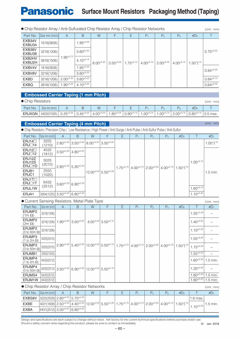
Design and specifications are each subject to change without notice. Ask factory for the current technical specifications before purchase and/or use.
Should a safety concern arise regarding this product, please be sure to contact us immediately.
Surface Mount Resistors Packaging Method (Taping)
– 60 –
Part No. Size mm (inch) A B W F E P1 P2 P0 0D0 T
EXB34VEXBU34
1616(0606)
1.95±0.15
1.95±0.20
8.00±0.20 3.50±0.05 1.75±0.10 4.00±0.10 2.00±0.05 4.00±0.10 1.50+0.10
0.70±0.05EXB38VEXBU38
3216(1206) 3.60±0.20
EXB2HVEXBU2H
3816(1506) 4.10±0.15
EXBV4V 1616(0606) 1.95±0.20
0.84±0.05
EXBV8V 3216(1206) 3.60±0.20
EXBD 3216(1206) 2.00±0.20 3.60±0.20 0.84±0.10
EXBQ 3816(1506) 1.90±0.20 4.10±0.20 0.64±0.05
0
● Chip Resistor Array / Anti-Sulfurated Chip Resistor Array / Chip Resistor Networks (Unit : mm)
Part No. Size mm (inch) A B W F E P1 P2 P0 0D0 T
ERJXGN 0402(01005) 0.25±0.05 0.45±0.05 4.00±0.20 1.80±0.05 0.90±0.10 1.00±0.10 1.00±0.10 2.00±0.10 0.80±0.10 0.5 max.
Embossed Carrier Taping (1 mm Pitch)
● Chip Resistors (Unit : mm)
Part No. Size mm (inch) A B W F E P1 P2 P0 0D0 T 0D1
ERJ14□ERJ□14
3225(1210)
2.80±0.20 3.50±0.20 8.00±0.30 3.50±0.05
1.75±0.10 4.00±0.10 2.00±0.05 4.00±0.10 1.50+0.10
1.00±0.10
1.00+0.10
ERJ12□ERJ□12
4532(1812)
3.50±0.20 4.80±0.20
12.00±0.30 5.50±0.20 1.5 min.
ERJ12ZERJ12SERJ□1D
5025(2010)
2.80±0.20 5.30±0.20
ERJB1ERJC1
2550(1020)
ERJ1T□ERJ□1T 6432
(2512)3.60±0.20 6.90±0.20
ERJL1W 1.60±0.10
ERJA1 3264(1225) 3.50±0.20 6.80±0.20 1.10±0.20
0
0
Embossed Carrier Taping (4 mm Pitch)
● Chip Resistors / Precision Chip / Low Resistance / High Power / Anti-Surge / Anti-Pulse / Anti-Sulfur Pulse / Anti-Sulfur
(Unit : mm)
● Chip Resistor Array / Chip Resistor Networks
Part No. Size mm (inch) A B W F E P1 P2 P0 0D0 T 0D1
EXBS8V 5022(2029) 2.80±0.20 5.70±0.20
12.00±0.30 5.50±0.20 1.75±0.10 4.00±0.10 2.00±0.05 4.00±0.10 1.50+0.10
1.6 max.
1.5 min.EXBE 4021(1608) 2.50±0.20 4.40±0.20
1.10±0.20
EXBA 6431(2512) 3.50±0.20 6.80±0.20
0
(Unit : mm)
● Current Sensing Resistors, Metal Plate Type (Unit : mm)
Part No. Size mm (inch) A B W F E P1 P2 P0 0D0 T 0D1
ERJMP2(1m Ω)
3216(1206)
1.90±0.20 3.50±0.20 8.00±0.30 3.50±0.10
1.75±0.10 4.00±0.10 2.00±0.05 4.00±0.10 1.50+0.10
1.55±0.20 −
ERJMP2(2m Ω)
3216(1206) 1.40±0.20 −
ERJMP2(3 to 50m Ω)
3216(1206) 1.10±0.20 −
ERJMP3(1 to 2m Ω)
5025(2010)
2.90±0.20 5.40±0.20 12.00±0.30 5.50±0.10
1.55±0.20 −
ERJMP3(3 to 50m Ω)
5025(2010) 1.15±0.20 −
ERJMB1 2550(1020) 1.55±0.20 −
ERJMP4(1 to 2m Ω)
6432(2512)
3.50±0.20 6.90±0.20 12.00±0.30 5.50±0.10
1.60±0.20 1.5 min.
ERJMP4(3 to 50m Ω)
6432(2512) 1.20±0.20 −
ERJMS4 6432(2512) 1.60±0.20 1.5 min.
ERJM1W 6432(2512) 1.80±0.20 1.5 min.
0
Jan. 201812

Design and specifications are each subject to change without notice. Ask factory for the current technical specifications before purchase and/or use.
Should a safety concern arise regarding this product, please be sure to contact us immediately.
Surface Mount Resistors Packaging Method (Taping)
– 61 –
fN
W2
W1
fA
fC Tape Width (W)
0A 0N 0C W1 W2
4mm Width 180.0±3.0
60.0+1.0
13.0±0.2
4.5±0.5 7.0±0.5
8mm Width 180.0 –1.5
9.0+1.0 11.4±1.0
12mm Width 13.0+1.0 15.4±1.0
24mm Width 380.0±2.0 80.0±1.0 25.4±1.0 29.4±1.0
00 0
0
(Unit : mm)
● Current Sensing Resistors, Metal Plate Type (Unit : mm)
Embossed Carrier Taping (8 mm Pitch)
Taping Reel
Part No. Size mm (inch) A B W F E P1 P2 P0 0D0 T 0D1
ERJMS6 6468(2526) 6.90±0.20 7.50±0.20 12.00±0.30 5.50±0.05 1.75±0.10 8.00±0.10 2.00±0.05 4.00±0.10 1.50+0.10 2.45±0.20 1.5 min.0
Jan. 201812
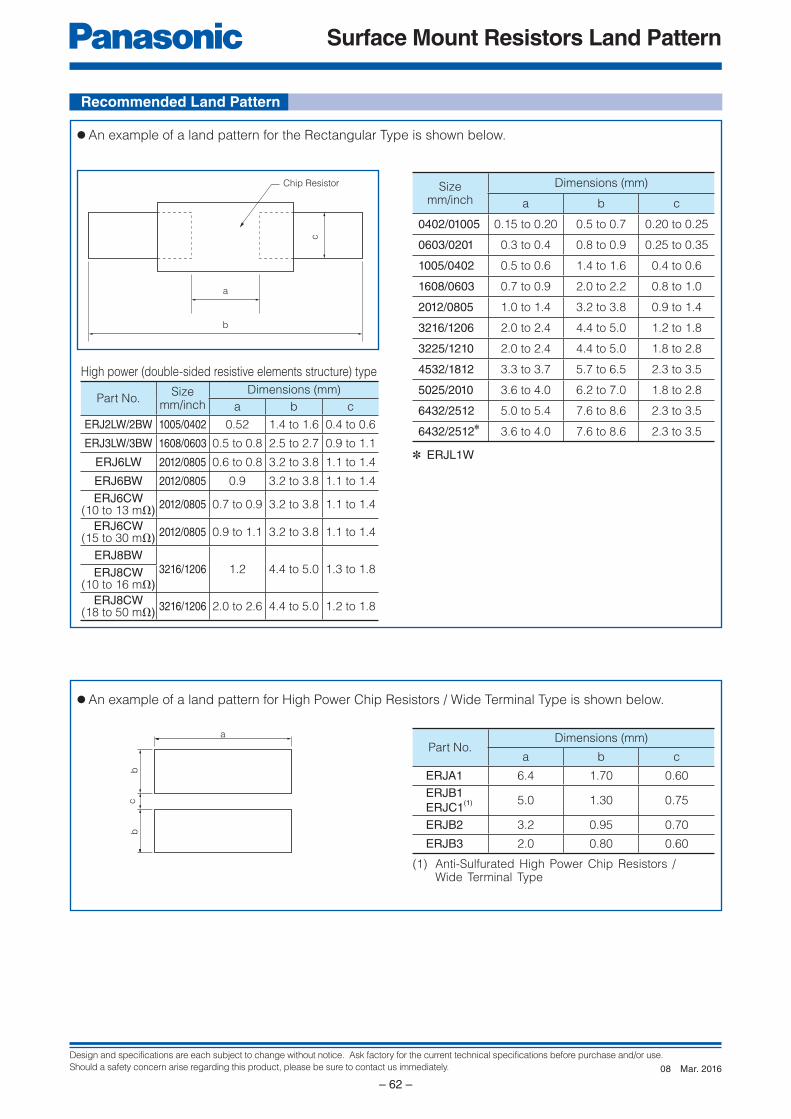
Design and specifications are each subject to change without notice. Ask factory for the current technical specifications before purchase and/or use.
Should a safety concern arise regarding this product, please be sure to contact us immediately.
Surface Mount Resistors Land Pattern
– 62 –
c
a
b
Chip Resistor
a
cb
b
Recommended Land Pattern
Sizemm/inch
Dimensions (mm)
a b c
0402/01005 0.15 to 0.20 0.5 to 0.7 0.20 to 0.25
0603/0201 0.3 to 0.4 0.8 to 0.9 0.25 to 0.35
1005/0402 0.5 to 0.6 1.4 to 1.6 0.4 to 0.6
1608/0603 0.7 to 0.9 2.0 to 2.2 0.8 to 1.0
2012/0805 1.0 to 1.4 3.2 to 3.8 0.9 to 1.4
3216/1206 2.0 to 2.4 4.4 to 5.0 1.2 to 1.8
3225/1210 2.0 to 2.4 4.4 to 5.0 1.8 to 2.8
4532/1812 3.3 to 3.7 5.7 to 6.5 2.3 to 3.5
5025/2010 3.6 to 4.0 6.2 to 7.0 1.8 to 2.8
6432/2512 5.0 to 5.4 7.6 to 8.6 2.3 to 3.5
6432/2512✽
3.6 to 4.0 7.6 to 8.6 2.3 to 3.5
✽ ERJL1W
● An example of a land pattern for High Power Chip Resistors / Wide Terminal Type is shown below.
Part No.Dimensions (mm)
a b c
ERJA1 6.4 1.70 0.60
ERJB1
ERJC1(1) 5.0 1.30 0.75
ERJB2 3.2 0.95 0.70
ERJB3 2.0 0.80 0.60
● An example of a land pattern for the Rectangular Type is shown below.
Part No.Size
mm/inch
Dimensions (mm)
a b c
ERJ2LW/2BW 1005/0402 0.52 1.4 to 1.6 0.4 to 0.6
ERJ3LW/3BW 1608/0603 0.5 to 0.8 2.5 to 2.7 0.9 to 1.1
ERJ6LW 2012/0805 0.6 to 0.8 3.2 to 3.8 1.1 to 1.4
ERJ6BW 2012/0805 0.9 3.2 to 3.8 1.1 to 1.4
ERJ6CW(10 to 13 mΩ)
2012/0805 0.7 to 0.9 3.2 to 3.8 1.1 to 1.4
ERJ6CW(15 to 30 mΩ)
2012/0805 0.9 to 1.1 3.2 to 3.8 1.1 to 1.4
ERJ8BW3216/1206 1.2 4.4 to 5.0 1.3 to 1.8ERJ8CW
(10 to 16 mΩ)
ERJ8CW(18 to 50 mΩ)
3216/1206 2.0 to 2.6 4.4 to 5.0 1.2 to 1.8
High power (double-sided resistive elements structure) type
(1) Anti-Sulfurated High Power Chip Resistors / Wide Terminal Type
Mar. 201608

Design and specifications are each subject to change without notice. Ask factory for the current technical specifications before purchase and/or use.
Should a safety concern arise regarding this product, please be sure to contact us immediately.
Surface Mount Resistors Land Pattern
– 63 –
a dcb
Conductor
Solder resist
f a
b
P
c
b bd d d d d d dc c c c c c
aff a
b d bc cd d
0.8
0.4
to 0
.5
3.3 to 3.45.0 to 5.4
0.35 to 0.4
1.4 to
1.5
3.1
to 3
.5
2.1
to 2
.5
4.3
to 4
.7
1.27 0.4 to 0.6
4.4
2.2
0.2
0.4 to 0.51.27
4.42.2
0.2
1.27
EXBA10P EXBA10E1.27 0.635 1.27 0.635
0.4 to 0.5
3.4
1.4
5.23.3
0.5
0.8 0.4 0.35 to 0.40.1 to 0.15
0.635
0.9 to
1.1
2.0
to 2
.6
0.3
to 0
.4
0.2 to 0.3
2.6 to 2.83.6 to 4.2
0.50
0.9
to 1
.1
2.0
to 2
.6
0.20 to 0.25
● An example of a land pattern for Chip Resistor Array, Anti-Sulfurated Chip Resistor Array and Chip Attenuator is shown below.
Part No.Dimensions (mm)
a b c d
EXB14VEXB14A
0.30 0.30 0.30 0.80 to 0.90
EXB24VEXBU24EXB24A
0.5 0.35 to 0.40 0.30 1.4 to 1.5
Part No.Dimensions (mm)
a b c f P
EXB18V 0.20 to 0.30 0.15 to 0.20 0.15 to 0.20 0.80 to 0.90 0.40
EXBV4V,V8V 0.7 to 0.9 0.4 to 0.45 0.4 to 0.45 2 to 2.4 0.80
EXB34V,38VEXBU34,U38
0.7 to 0.9 0.4 to 0.5 0.4 to 0.5 2.2 to 2.6 0.80
EXBS8V 1 to 1.2 0.5 to 0.75 0.5 to 0.75 3.2 to 3.8 1.27
Part No.Dimensions (mm)
a b c d f
EXB28VEXBU28
0.40 0.525 0.25 0.25 1.40
EXBN8V 0.45 to 0.50 0.35 to 0.38 0.25 0.25 1.40 to 2.00
Part No.Dimensions (mm)
a b c d f
EXB2HVEXBU2H
1.00 0.425 0.25 0.25 2.00
✽ When designing high density land patterns, examine the reliability of isolation among the lines and adopt the chip resistor networks.
EXBA EXBE
For popular pattern
Pitch 1.27 mm Pitch 0.8 mm
For high density pattern
✽
Pitch 0.635 mmThrough-hole less
Pitch 0.4 mmThrough-hole less
EXBD EXBQ
For popular pattern
Pitch 0.635 mm Pitch 0.5 mm
● An example of a land pattern for Chip Resistor Networks is shown below.
Mar. 201608

Design and specifications are each subject to change without notice. Ask factory for the current technical specifications before purchase and/or use.
Should a safety concern arise regarding this product, please be sure to contact us immediately.
Surface Mount Resistors Recommended Soldering Conditions
– 64 –
Preheating
Peak
Heating
Tem
pe
ratu
re
Time
Preheating
Peak
Heating
Tem
pera
ture
Time
Recommended Soldering Conditions
● Flow soldering We do not recommend flow soldering, because a solder bridge may form. Please contact us regarding flow sol der ing of EXBA se ries.
Temperature Time
Preheating 140 °C to 160 °C 60 s to 120 s
Main heating Above 200 °C 30 s to 40 s
Peak 235 ± 5 °C max. 10 s
Temperature Time
Preheating 150 °C to 180 °C 60 s to 120 s
Main heating Above 230 °C 30 s to 40 s
Peak max. 260 °C max. 10 s
For soldering For lead-free soldering
Temperature Time Temperature Time
Preheating 140 °C to 180 °C 60 s to 120 s 150 °C to 180 °C 60 s to 120 s
Soldering 245 ± 5 °C 20 s to 30 s max. 260 °C max. 10 s
For soldering (Example : Sn/Pb)
For lead-free soldering (Example : Sn/Ag/Cu)
● Recommended soldering conditions for fl ow
● Recommended soldering conditions for reflow
· Reflow soldering shall be performed a maximum of two times. · Please contact us for additional information when used in conditions other than those specified. · Please measure the temperature of the terminals and study every kind of solder and printed circuit board for solderability be fore ac tu al use.
Temperature Time
Preheating 140 °C to 160 °C 60 s to 120 s
Main heating Above 200 °C 30 s to 40 s
Peak 235 ± 5 °C max. 10 s
Temperature Time
Preheating 150 °C to 180 °C 60 s to 120 s
Main heating Above 230 °C 30 s to 40 s
Peak max. 260 °C max. 10 s
For soldering (Example : Sn/Pb)
For lead-free soldering (Example : Sn/Ag/Cu)
● Chip Resistor Array, Chip Resistor Networks and Chip Attenuator
● Rectagular Type
Recommendations and precautions are described below.
Sep. 201402
Design and specifications are each subject to change without notice. Ask factory for the current technical specifications before purchase and/or use.
Should a safety concern arise regarding this product, please be sure to contact us immediately.
Surface Mount Resistors Safety precautions
– 65 –
Safety Precautions (Common precautions for Surface Mount Resistors)
The following are precautions for individual products. Please also refer to the common precautions for Fixed Resistors
in this catalog.
1. Take measures against mechanical stress during and after mounting of Surface Mount Resistors (hereafter called the
resistors) so as not to damage their electrodes and protective coatings.
Be careful not to misplace the resistors on the land patterns. Otherwise, solder bridging may occur.
2. Keep the rated power and ambient temperature within the specified derating curve.
Some circuit boards, wiring patterns, temperatures of heat generated by adjacent components, or am bi ent
tem per a tures can become factors in the rise of the temperature of the re sis tors, regardless of the level of power
applied. Therefore, check the conditions before use and op ti mize them so as not to damage the boards and peripheral
components.
Make sure to contact us before using the resistors under special conditions.
3. If a transient load (heavy load in a short time) like a pulse is expected to be applied, check and evaluate the
operations of the resistors when installed in your products before use.
Never exceed the rated power. Otherwise, the performance and/or reliability of the resistors may be impaired.
4. Before using halogen-based or other high-activity flux, check the possible effects of the flux residues on the
per for mance and reliability of the resistors.
5. When soldering with a soldering iron, never touch the resistors'bodies with the tip of the soldering iron. When using a
soldering iron with a high temperature tip, finish soldering as quickly as possible (within three seconds at 350 °C max.).
6. As the amount of applied solder becomes larger, the mechanical stress applied to the resistors increases, causing
problems such as cracks and faulty characteristics. Avoid applying an excessive amounts of solder.
7. When the resistors' protective coatings are chipped, flawed, or removed, the characteristics of the resistors may be
impaired. Take special care not to apply mechanical shock during automatic mounting or cause damage during
handling of the boards with the resistors mounted.
8. Do not apply shock to the resistors or pinch them with a hard tool (e.g. pliers and tweezers). Otherwise, the resistors'
protective coatings and bodies may be chipped, affecting their performance.
9. Avoid excessive bending of printed circuit boards in order to protect the resistors from abnormal stress.
10. Do not immerse the resistors in solvent for a long time. Before using solvent, carefully check the effects of im mer sion.
11. Transient voltage
If there is a possibility that the transient phe nom e non (significantly high voltage ap plied in a short time) may
oc cur or that a high voltage pulse may be applied, make sure to evaluate and check the char ac ter is tics of
Fixed Metal (Oxide) Film Resistors mounted on your product rather than only depending on the calculated
pow er limit or steady-state conditions to complete the de sign or decide to use the resistors.
12. Do not apply excessive tension to the terminals.
Sep. 201402

Design and specifications are each subject to change without notice. Ask factory for the current technical specifications before purchase and/or use.
Should a safety concern arise regarding this product, please be sure to contact us immediately.
Metal (Oxide) Film Resistors
– 66 –
Product Code
ERXMetal Film Resistors
121235
0.5 W1 W2 W3 W5 W
Power Rating at 70 °C
S
F
Small size0.5 W to 5 W
Small size Anti-heatconducting type(Fe lead wire)1 W to 5 W
Style · Specification
JG
±5 %±2 %
Resistance Tolerance
Resistance Value
E
1
R
2
X
3 4
2
5
S Z W
6
J
7 8
1
9
R
10
0 E
11 12
□···□□···P□···VU···V□···EW···E□··HS···E
Straight lead wire typeCut & Forming typeAxial taping type (Straight lead)Axial taping type (Stand off)Radial taping type (E type)Radial taping type (WE type)Cut & Forming type Radial taping type (SE type)
The first two digits are significant figuresof resistance and the third one denotesnumber of zeros following.Decimal point is expressed by(Ex.) 1R0 : 1.0 Ω
ERX12S ±5 % 0.10 to 0.18 0.20 to 9.1
±2 % 0.10 to 0.91 1.0 to 9.1ERX1S ±5 % 0.10 to 0.18 0.20 to 9.1ERX1F ±2 % 0.10 to 0.91 1.0 to 9.1ERX2S ±5 % 0.10 to 0.20 0.22 to 9.1ERX2F ±2 % 0.10 to 0.91 1.0 to 9.1ERX3S ±5 % 0.10 to 0.20 0.22 to 9.1ERX3F ±2 % 0.10 to 0.91 1.0 to 9.1ERX5S ±5 % — 0.33 to 9.1ERX5F ±2 % 1.0 to 9.1
Part No.
Resistance Resistance Value Range (Ω) Tolerance ERX□□SZ ERX□□S Forming / Packaging
The matrix of forming and packaging is as shown in the table below.“Z” is added according to resistance.Forming & Taping matrix
Code 12S 1S 2S 3S 5S 1F 2F 3F 5F
○ ○ ○ ○ ○ ○ ○ ○ ○ ○ ○ ○ ○ ○ ○ ○ ○ ○ ○ ○ ○ ○ ○ ○ ○ ○ ○ ○ ○ ○ ○ ○ ○ ○ ○ ○ ○ ○
Product Code
ERGMetal Oxide
Film Resistors121235
0.5 W1 W2 W3 W5 W
Power Rating at 70 °C
S
F
Small size0.5 W to 5 WSmall size Anti-heatconducting type (Fe lead wire)1 W to 5 W
Style · Specification
JG
±5 %±2 %
Resistance Tolerance
Resistance Value
E
1
R
2
G
3 4
2
5
S W
6
J
7 8
1
9
0
10
3 E
11 12
□···□□···P□···VU···V□···EW···E□···HS···E
Straight lead wire typeCut & Forming typeAxial taping type(Straight lead)Axial taping type(Stand off)Radial taping type(E type)Radial taping type(WE type)Cut & Forming typeRadial taping type(SE type)
The first two digits are significant figuresof resistance and the third one denotesnumber of zeros following.Decimal point is expressed by(Ex.) 103 : 10 kΩ
Forming / Packaging
The matrix of forming and packaging is as shown in the table below.
Forming & Taping matrixCode
12S 1S 2S 3S 5S 1F 2F 3F 5F
○ ○ ○ ○ ○ ○ ○ ○ ○ ○ ○ ○ ○ ○ ○ ○ ○ ○ ○ ○ ○ ○ ○ ○ ○ ○ ○ ○ ○ ○ ○ ○ ○ ○ ○ ○ ○ ○ ○
Explanation of Part Numbers
Features
● Miniaturized 50 % smaller compared to existing models● Non-fl ammable● High Reliability● Automatic Insertion● Reference Standards IEC 60115-2, IEC 60115-4, JIS C 5201-4, EIAJ RC-2138● RoHS compliant
Metal (Oxide) Film Re sis tors
Type: ERG(X)S (Small size) (0.5 W, 1 W, 2 W, 3 W, 5 W)
ERG(X)F (Anti-heat conducting for PCB) (1 W, 2 W, 3 W, 5 W)
Ex.1 : ERX type
The above example 1 shows a small metal film resistor, 2 W power rating, resistance value of 1.0 Ω, tolerance ±5 %, and package of radial taping.
The above example 2 shows a small metal oxide film resistor, 2 W power rating, resistance value of 10 kΩ, tolerance ±5 %, and package of radial taping.
Ex.2 : ERG type
Sep. 201402

Design and specifications are each subject to change without notice. Ask factory for the current technical specifications before purchase and/or use.
Should a safety concern arise regarding this product, please be sure to contact us immediately.
Metal (Oxide) Film Resistors
– 67 –
fd
fDkk L
–60 –40 –20 0 20 40 60 80 100 120 140 160 180 200 220 2400
20
40
60
80
100
120
130 °C
70 °C–55 °C
ERG(X)12S
ERG(X)1S, 1F
ERG(X)3S, 3F
ERG(X)5S, 5F
235 °C
Ambient Temperature (°C)
Rate
d L
oad
(%
)
ERG(X)2S, 2F
Power Derating CurveFor resistors operated in ambient temperatures above 70 °C, power rating shall be derated in accordance with the figure on the right.
Ratings
Part No.
Power
Rating
at 70 °C
(W)
Limiting
Element
Voltage(1)
(V)
Maximum
Overload
Voltage(2)
(V)
Maximum
Intermittent
Overload
Voltage(3)
(V)
Dielectric
With stand ing
Voltage
(VAC)
Res.
Tol.
(%)(4)
Resistance
Range (Ω)(5) T.C.R.
(×10–6
/°C)
Standard
Resistance
Valuemin.
(6)max.
ERG(X)12S 0.5 300 600 600 350G (±2) 1 22 k
±350 E24J (±5) 0.2 47 k
ERG(X)1S
ERG(X)1F1 350 600 600 350
G (±2) 1 68 k±350 E24
J (±5) 0.2 100 k
ERG(X)2S
ERG(X)2F2 350 700 1000 600
G (±2) 1 100 k±350 E24
J (±5) 0.22 100 k
ERG(X)3S
ERG(X)3F3 350 700 1000 1000
G (±2) 1 100 k±300 E24
J (±5) 0.22 100 k
ERG(X)5S
ERG(X)5F5 500 1000 1500 1000
G (±2) 1 100 k±200 E24
J (±5) 0.33 100 k
Part No.Dimensions (mm) Mass
(Weight)
[g/pc.]L 0D k 0d
ERG(X)12S 6.35+0.65
2.3+0.5
30.0±3.0
0.65±0.05
0.26
ERG(X)1S9.00
+1.502.8
±0.530.0
±3.00.65
±0.05
0.33ERG(X)1F 0.80
±0.05
ERG(X)2S
ERG(X)2F12.00
+1.504.0
±1.030.0
±3.00.80
±0.050.66
ERG(X)3S
ERG(X)3F15.00
±1.505.5
±1.038.0
±3.00.80
±0.051.47
ERG(X)5S
ERG(X)5F24.00
±1.508.0
±1.038.0
±3.00.80
±0.053.54
–0.3–0.35
–1.00
–1.00
Code Part No. Res.Tol. Res. Value Range Code Part No. Res.Tol. Res. Value Range
Z
12S±2 % 0.1 to 0.91 Ω
Z
2S
2F
±2 % 0.1 to 0.91 Ω
±5 % 0.1 to 0.18 Ω ±5 % 0.1 to 0.2 Ω
1S
1F
±2 % 0.1 to 0.91 Ω 3S
3F
±2 % 0.1 to 0.91 Ω
±5 % 0.1 to 0.18 Ω ±5 % 0.1 to 0.2 Ω
(1) Rated Continuous Working Voltage (RCWV) shall be determined from RCWV=√Power Rating×Resistance Value or Limiting Element Voltage listed above whichever less.
(2) Overload (Short-time Overload) Test Voltage (SOTV) shall be determined from SOTV=2.5×Power Rating or max. Overload Voltage listed above whichever less.
(3) Intermittent Overload Test Voltage (IOTV) shall be determined from IOTV=4.0×Power Rating or max. Intermittent Overload Voltage listed above whichever less.
(4) Resistance tolerance is of use besides range listed, please inquire.(5) Resistance Range Type ERG : >10 Ω Type ERX : <9.1 Ω(6) As for the low resistance value range, "Z" is given to the part
number. (Refer to the explanation of part numbers.)
✽ Z type is non standard resistance values.
High reliable metal oxide fi lm (ERG)High reliable metal plating fi lm(ERX)
Flame and solvent retardant
End cap
Spi ral ling turns
Ceramic core(High ther mal con duc tiv i ty)
Lead wireS type : Cu wireF type : Fe wire( )
Marking
Construction Dimensions in mm (not to scale)
Sep. 201402
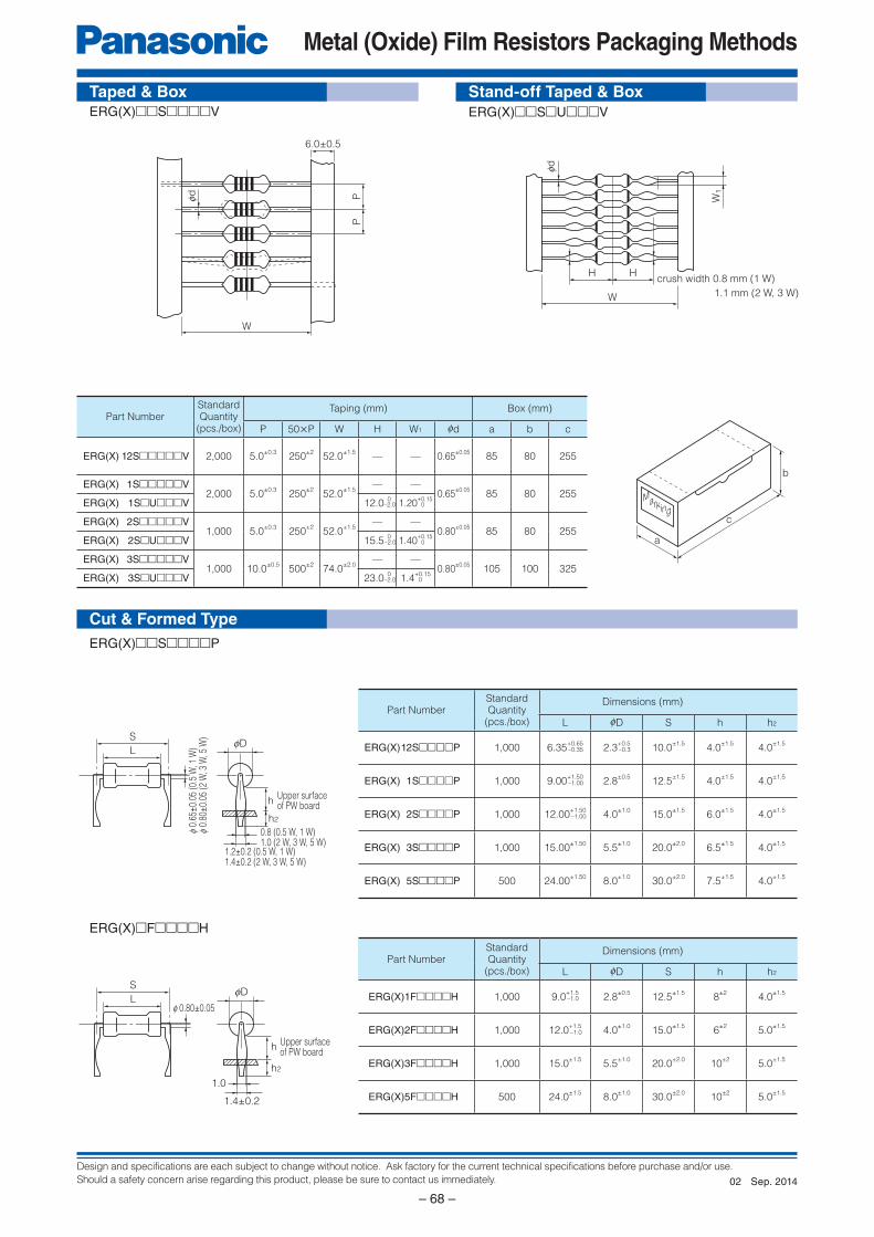
Design and specifications are each subject to change without notice. Ask factory for the current technical specifications before purchase and/or use.
Should a safety concern arise regarding this product, please be sure to contact us immediately.
Metal (Oxide) Film Resistors Packaging Methods
– 68 –
Marking
a
b
c
6.0±0.5
W
PPfd
crush width 0.8 mm (1 W)
1.1 mm (2 W, 3 W)
H H
W
W1
fd
S
Lf 0.80±0.05
1.0
1.4±0.2
fD
Upper surfaceof PW board
h
h2
S
LfD
Upper surfaceof PW board
h
0.8 (0.5 W, 1 W)1.0 (2 W, 3 W, 5 W)
1.2±0.2 (0.5 W, 1 W)1.4±0.2 (2 W, 3 W, 5 W)
f 0.6
5±0.
05 (0
.5 W
, 1 W
)f 0
.80±
0.05
(2 W
, 3 W
, 5 W
)
h2
Taped & Box
Cut & Formed Type
Stand-off Taped & BoxERG(X)□□S□□□□V ERG(X)□□S□U□□□V
Part NumberStandardQuantity
(pcs./box)
Dimensions (mm)
L 0D S h h2
ERG(X) 12S□□□□P 1,000 6.35+0.65
2.3+0.5
10.0±1.5
4.0±1.5
4.0±1.5
ERG(X) 1S□□□□P 1,000 9.00+1.50
2.8±0.5
12.5±1.5
4.0±1.5
4.0±1.5
ERG(X) 2S□□□□P 1,000 12.00+1.50
4.0±1.0
15.0±1.5
6.0±1.5
4.0±1.5
ERG(X) 3S□□□□P 1,000 15.00±1.50
5.5±1.0
20.0±2.0
6.5±1.5
4.0±1.5
ERG(X) 5S□□□□P 500 24.00±1.50
8.0±1.0
30.0±2.0
7.5±1.5
4.0±1.5
–1.00
–1.00
–0.35 –0.3
Part NumberStandardQuantity
(pcs./box)
Dimensions (mm)
L 0D S h h2
ERG(X)1F□□□□H 1,000 9.0+1.5
2.8±0.5
12.5±1.5
8±2
4.0±1.5
ERG(X)2F□□□□H 1,000 12.0+1.5
4.0±1.0
15.0±1.5
6±2
5.0±1.5
ERG(X)3F□□□□H 1,000 15.0±1.5
5.5±1.0
20.0±2.0
10±2
5.0±1.5
ERG(X)5F□□□□H 500 24.0±1.5
8.0±1.0
30.0±2.0
10±2
5.0±1.5
–1.0
ERG(X)□□S□□□□P
ERG(X)□F□□□□H
Part NumberStandardQuantity
(pcs./box)
Taping (mm) Box (mm)
P 50×P W H W1 0d a b c
ERG(X) 12S□□□□□V 2,000 5.0±0.3
250±2
52.0±1.5
— — 0.65±0.05
85 80 255
ERG(X) 1S□□□□□V2,000 5.0
±0.3250
±252.0
±1.5— —
0.65±0.05
85 80 255ERG(X) 1S□U□□□V 12.0
01.20
+0.15
ERG(X) 2S□□□□□V1,000 5.0
±0.3250
±252.0
±1.5— —
0.80±0.05
85 80 255ERG(X) 2S□U□□□V 15.5
01.40
+0.15
ERG(X) 3S□□□□□V1,000 10.0
±0.5500
±274.0
±2.0— —
0.80±0.05
105 100 325ERG(X) 3S□U□□□V 23.0
01.4
+0.15–2.0
–2.0
–2.0 0
0
0
–1.0
Sep. 201402

Design and specifications are each subject to change without notice. Ask factory for the current technical specifications before purchase and/or use.
Should a safety concern arise regarding this product, please be sure to contact us immediately.
Metal (Oxide) Film Resistors Packaging Methods
– 69 –
a
b
cMarking
P1 P
A B
FP2
H1
H0
W1
W
fd
fD
P0fD0
P0 fD0
fd
W
H1P1F
P P2
fD
A
InsulatedLead
W1
H0
ERG(X)□□S□□□□E (12S, 1S, 2S)
ERG(X)□□S□W□□□E (12S, 1S, 2S, 3S)
Dimensions (mm) Dimensions (mm) Dimensions (mm) Dimensions (mm) Dimensions (mm)
P 12.7±1.0 W 18.0±0.5
H1
12S 32 max.
A
12S 6.35+0.65
0D
12S 2.3+0.5
P0 12.7±0.3 W1 9.0±0.5 1S 32 max. 1S 9.0+1.5
1S 2.8±0.5
P1 3.85±0.70 2S 38 max. 2S 12.0+1.5
2S 4.0±1.0
P2 6.35±1.00 H0 16.0±0.5 0d 0.65±0.05
F 5.0±0.8 0D0 4.0±0.2
–0.3–0.35
–1.0
–1.0
Part NumberDimensions (mm) Standard Quantity
(pcs./box)a b c
ERG(X) 12S□□□□E 46 130 335 2,000
ERG(X) 1S□□□□E 46 130 335 2,000
ERG(X) 2S□□□□E 49 100 335 1,000
● Radial Tape Package Specifi cations
–0.35
–1.0
–1.0
–0.3
Dimensions (mm) Dimensions (mm)
P12S 12.7±1.0 0D0 12S, 1S, 2S, 3S 4.0±0.2
1S, 2S, 3S 30.0±1.0
A
12S 6.35+0.65
P0
12S 12.7±0.3 1S 9.0+1.5
1S, 2S, 3S 15.0±0.3 2S 12.0+1.5
P1
12S 6.35±1.00 3S 15.0±1.5
1S, 2S, 3S 7.5±1.0
B
12S 11.2 max.
P2
12S 3.85±0.70 1S 14.0 max.
1S, 2S, 3S 3.75±0.50 2S 17.0 max.
F12S 5.0±0.5 3S 21.0 max.
1S, 2S, 3S 7.5±0.8
0D
12S 2.3+0.5
W 12S, 1S, 2S, 3S 18.0±0.5 1S 2.8±0.5
W1 12S, 1S, 2S, 3S 9.0±0.5 2S 4.0±1.0
H0
12S 16.0±0.5 3S 5.5±1.0
1S, 2S 18.0±1.00d
12S 00.65±0.05
3S 19.0±1.0 1S, 2S, 3S 00.80±0.05
H1
12S 6.5+0.6
1S, 2S 6.5+1.0
3S 8.0+1.0
0
0
0
For Panasert Au to mat ic Insertion Machine Radial Taped & Box
For Panasert Automatic Insertion Machine Radial Taped & Box
Sep. 201402
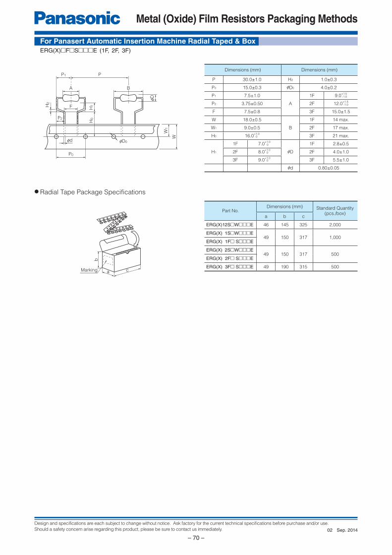
Design and specifications are each subject to change without notice. Ask factory for the current technical specifications before purchase and/or use.
Should a safety concern arise regarding this product, please be sure to contact us immediately.
Metal (Oxide) Film Resistors Packaging Methods
– 70 –
P1 P
F
P2
H2
H1
H0
fd
P0
fD0
fD
W1
W
A B
a
b
cMarking
ERG(X)□F□S□□□E (1F, 2F, 3F)
Part No.Dimensions (mm) Standard Quantity
(pcs./box)a b c
ERG(X) 12S□ W□□□E 46 145 325 2,000
ERG(X) 1S□ W□□□E49 150 317 1,000
ERG(X) 1F□ S□□□E
ERG(X) 2S□ W□□□E49 150 317 500
ERG(X) 2F□ S□□□E
ERG(X) 3F□ S□□□E 49 190 315 500
● Radial Tape Package Specifi cations
Dimensions (mm) Dimensions (mm)
P 30.0±1.0 H2 1.0±0.3
P0 15.0±0.3 0D0 4.0±0.2
P1 7.5±1.0
A
1F 9.0+1.5
P2 3.75±0.50 2F 12.0+1.5
F 7.5±0.8 3F 15.0±1.5
W 18.0±0.5
B
1F 14 max.
W1 9.0±0.5 2F 17 max.
H0 16.0+1.0
3F 21 max.
H1
1F 7.0+1.0
0D
1F 2.8±0.5
2F 8.0+1.0
2F 4.0±1.0
3F 9.0+1.0
3F 5.5±1.0
0d 0.80±0.05
–1.0
–1.0
0
0
0
0
For Panasert Automatic Insertion Machine Radial Taped & Box
Sep. 201402
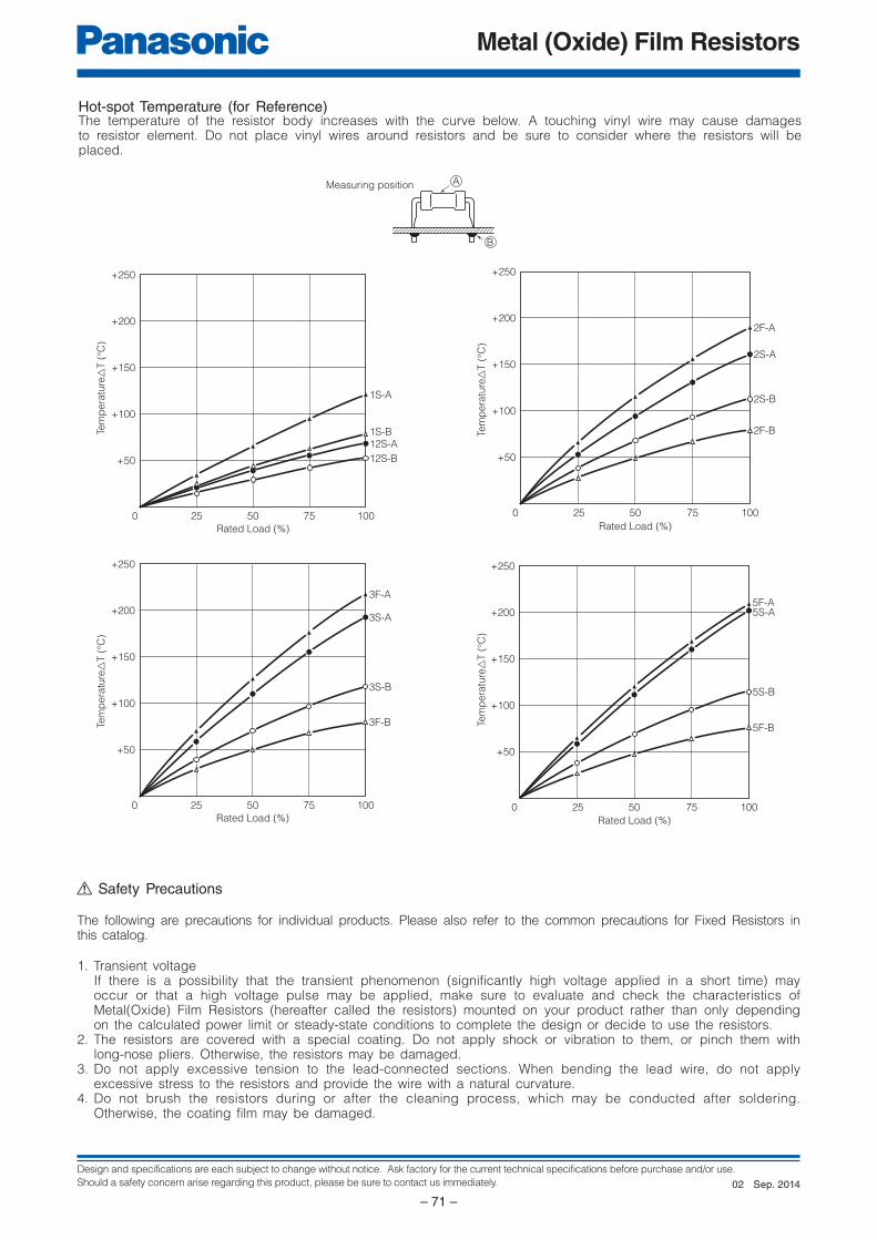
Design and specifications are each subject to change without notice. Ask factory for the current technical specifications before purchase and/or use.
Should a safety concern arise regarding this product, please be sure to contact us immediately.
Metal (Oxide) Film Resistors
– 71 –
A
B
Measuring position
25 50 75 1000
+50
+100
+150
+200
+250
Rated Load (%)
Tem
pe
ratu
re△
T (
°C)
1S-A
1S-B12S-A
12S-B
25 50 75 1000
+50
+100
+150
+200
+250
Rated Load (%)
Tem
pe
ratu
re△
T (
°C)
2F-A
2S-A
2S-B
2F-B
25 50 75 1000
+50
+100
+150
+200
+250
Rated Load (%)
Tem
pera
ture
△T (
°C)
3F-A
3S-A
3S-B
3F-B
25 50 75 1000
+50
+100
+150
+200
+250
Rated Load (%)
Tem
pera
ture
△T (
°C)
5F-A5S-A
5S-B
5F-B
Hot-spot Temperature (for Reference)The temperature of the resistor body increases with the curve below. A touching vinyl wire may cause damages to resistor element. Do not place vinyl wires around resistors and be sure to consider where the resistors will be placed.
Safety Precautions
The following are precautions for individual products. Please also refer to the common precautions for Fixed Resistors in this catalog.
1. Transient voltageIf there is a possibility that the transient phenomenon (significantly high voltage applied in a short time) may occur or that a high voltage pulse may be applied, make sure to evaluate and check the characteristics of Metal(Oxide) Film Resistors (hereafter called the resistors) mounted on your product rath er than only dependingon the calculated pow er limit or steady-state conditions to complete the design or decide to use the resistors.
2. The resistors are covered with a special coating. Do not apply shock or vibration to them, or pinch them with long-nose pliers. Otherwise, the resistors may be damaged.
3. Do not apply excessive tension to the lead-connect ed sections. When bending the lead wire, do not applyexcessive stress to the resistors and provide the wire with a natural curvature.
4. Do not brush the resistors during or after the cleaning process, which may be conducted after soldering.Otherwise, the coating film may be damaged.
Sep. 201402

Design and specifications are each subject to change without notice. Ask factory for the current technical specifications before purchase and/or use.
Should a safety concern arise regarding this product, please be sure to contact us immediately.
Metal (Oxide) Film Resistors
– 72 –
t
T
PP (VP)
Part No. K Vp max. (V)
ERG(X) 12S 0.5 600
ERG(X) 1S 0.5 600
ERG(X) 2S 0.5 700
ERG(X) 3S 0.5 700
ERG(X) 5S 0.5 1000
PP : Pulse limit power (W)
VP : Pulse limit voltage (V)
t : Pulse continuous time (s)
T : Period (s)
VR : Rated voltage (V)
P : Rated power (W)
R : Resistance value (Ω)
Vp max. : Max. pulse limit volt age (V)
(Data for Reference)
● T>1(s) → T=1(s)● T/t>100 → T/t=100● PP<P → P stands for PP
(VP<VR → VR stands for VP)● Added voltage<Vp max.
● PP or VP is referent value Conditions: Pulse added time=1000 h Resistance change=±5 % Room temperature
Withstand pulse limit power is calculated by the next
method.
PP = K·P·T/tVP =√K·P·R·T/tReference to the right about a fixed number of VP max.
Pulse Char ac ter is tics (Usual)
Sep. 201402

Design and specifications are each subject to change without notice. Ask factory for the current technical specifications before purchase and/or use.
Should a safety concern arise regarding this product, please be sure to contact us immediately.
Anti-Pulse Power Resistors
– 73 –
E
1
R
2
G
3 4
2
5
D
6
J
7 8
2
9
2
10
4
11 12
12
1
2
3
0.5 W
1 W
2 W
3 W
Power Rating Product Code
G
J
±2 %
±5 %
Resistance Tolerance
Resistance Value
The first two digits are significant figures of resistance and the third one denotes number of zeros following.
(Ex.) 224 : 220 kΩ
Anti-PulsePower Resistors
Forming &Taping matrixCode
□···□□···V
□···P
U···V
□···E
W···E
Straight lead wire type
Axial paping type (Straight lead)
Cut & Forming type
Axial paping type (Stand off)
Radial Taping type (E type)
Radial Taping type (WE type)
Forming / Packaging 12D 1D 2D 3D
○ ○ ○ ○ ○ ○ ○ ○ ○ ○ ○ ○ ○ ○ ○ ○ ○ ○ ○ ○ ○
fd
fDkk L
Explanation of Part Numbers
Features
● Miniaturized● Non-fl ammable● Anti-Pulse Characteristic● Automatic Insertion● RoHS compliant
Anti-Pulse Power Resistors
Type: ERGD (0.5 W, 1 W, 2 W, 3 W)
The above example shows an anti-pulse resistor, 2 W pow er rat ing, re sis tance value of 220 k ohms, tolerance ±5 %, and pack age of stan dard bulk
packing.
High reliable special fi lm Lead wire
Marking
Flame and solvent retardant
End cap
Spi ral ling turns
Ceramic core(High ther mal con duc tiv i ty)
Part No.Dimensions (mm) Mass
(Weight)[g/pc.]L 0D k 0d
ERG12D 6.35+0.65
2.3+0.5
30.0±3.0
0.65±0.05
0.26
ERG1D 9.00+1.50
2.8±0.5
30.0±3.0
0.65±0.05
0.33
ERG2D 12.00+1.50
4.0±1.0
30.0±3.0
0.80±0.05
0.66
ERG3D 15.00±1.50
5.5±1.0
38.0±3.0
0.80±0.05
1.47
–0.3–0.35
–1.00
–1.00
Construction Dimensions in mm (not to scale)
Sep. 201402

Design and specifications are each subject to change without notice. Ask factory for the current technical specifications before purchase and/or use.
Should a safety concern arise regarding this product, please be sure to contact us immediately.
Anti-Pulse Power Resistors
– 74 –
–60 –40 –20 0 20 40 60 80 100 120 140 160 180 200 220 2400
20
40
60
80
100
120
130 °C
70 °C–55 °C
ERG12D
235 °C
Ambient Temperature (°C)
Rate
d L
oad
(%
)
ERG1D ~ 3D
Power Derating CurveFor resistors operated in ambient temperatures above 70 °C, power rating shall be derated in accordance with the figure on the right.
Ratings
Safety Precautions
The following are precautions for individual products. Please also refer to the common precautions for Fixed Resistors
in this catalog.
1. Transient voltage
If there is a possibility that the transient phenomenon (significantly high volt age applied in a short time) may
occur or that a high voltage pulse may be applied, make sure to evaluate and check the characteristics of
Anti-Pulse Power Resistors (hereafter called the resistors) mount ed on your product rather than only depending on
the calculated power limit or steady-state conditions to complete the design or decide to use the resistors.
2. The resistors are covered with a special coating. Do not ap ply shock or vibration to them, or pinch them with
long-nose pliers. Otherwise, the resistors may be damaged.
3. Do not apply excessive tension to the lead-connect ed sections. When bend ing the lead wire, do not apply
excessive stress to the resistors and provide the wire with a natural curvature.
4. Do not brush the resistors during or after the cleaning process, which may be conducted after soldering.
Otherwise, the coating film may be damaged.
Part No.
PowerRating
at 70 °C(W)
LimitingElement Voltage
(1)
(V)
MaximumOverloadVoltage
(2)
(V)
MaximumIntermittentOverloadVoltage
(3)
(V)
DielectricWith stand ing
Voltage
(VAC)
Res.Tol.(%)
ResistanceRange (Ω)
(4)Standard
ResistanceValue
min. max.
ERG12D 0.5 400 800 800 500J (±5)G (±2)
51 k 240 k E24
ERG1D 1 500 1000 1000 500J (±5)G (±2)
110 k 330 k E24
ERG2D 2 500 1000 1000 700J (±5)G (±2)
110 k 510 k E24
ERG3D 3 500 1000 1000 700J (±5)G (±2)
110 k 750 k E24
(1) Rated Continuous Working Voltage (RCWV) shall be determined from RCWV=√Power Rating×Resistance Val ue or Limiting Element Voltage list ed above whichever less.
(2) Overload (Short-time Overload) Test Voltage (SOTV) shall be determined from SOTV=2.5×Power Rating or max. Overload Volt age list ed above which ev er less.
(3) Intermittent Overload Test Voltage (IOTV) shall be determined from IOTV=4.0×Power Rating or max. Intermittent Over load Volt age listed above whichever less.
(4) Resistance tolerance and resistance range is of use besides range listed, please inquire.
■ As for Packaging Methods and / or cut formed leads, Please see Metal (Oxide) Film Resistors Packaging Methods
Sep. 201402

Design and specifications are each subject to change without notice. Ask factory for the current technical specifications before purchase and/or use.
Should a safety concern arise regarding this product, please be sure to contact us immediately.
Metal Film Resistors, Low Re sis tance Value
– 75 –
E
1
R
2
X
3 4
2
5
L
6
J
7 8
4
9
7
10
M
11 12
12
1
2
0.5 W
1 W
2 W
Power Rating
ERXMetal Film Resistors
Product Code Special Feature
L
Small size
Low
resistance
value
J ±5 %
Resistance Tolerance
Resistance Value Forming &Taping matrixCode
□···□□···V
□···P
□···E
W···E
Straight lead wire type
Axial paping type (Straight lead)
Cut & Forming type
Radial Taping type (E type)
Radial Taping type (WE type)
Forming / PackagingThe first two digits are significant figures of resistance and it shows by the unit of the "mΩ". Decimal point is expressed by M as 47 mΩ = 47M.
12L 1L 2L
○ ○ ○ ○ ○ ○ ○ ○ ○ ○ ○ ○ ○ ○ ○
fd
fDkk L
Explanation of Part Numbers
Features
● Miniaturized● Non-fl ammable● Automatic Insertion● RoHS compliant
The above example shows a small size and low resistance value met al film re sis tor, 2 W pow er rat ing, resistance value of 47 m ohms, tol er ance ±5 %,
and pack age of standard bulk packing.
Construction Dimensions in mm (not to scale)
High reliable metal plating fi lm Lead wire
Marking
Flame and solvent retardant
End cap
Spiral ling turns
Ceramic core(High ther mal con duc tiv i ty)
Part No.Dimensions (mm) Mass
(Weight)[g/pc.]L 0D k 0d
ERX12L 6.35+0.65
2.3+0.5
30.0±3.0
0.65±0.05
0.26
ERX1L 9.00+1.50
2.8±0.5
30.0±3.0
0.65±0.05
0.33
ERX2L 12.00+1.50
4.0±1.0
30.0±3.0
0.80±0.05
0.66
–0.3–0.35
–1.00
–1.00
Metal Film Re sis tors
Type: ERXL (Low Resistance Value) (0.5 W, 1 W, 2 W)
Sep. 201402

Design and specifications are each subject to change without notice. Ask factory for the current technical specifications before purchase and/or use.
Should a safety concern arise regarding this product, please be sure to contact us immediately.
Metal Film Resistors, Low Re sis tance Value
– 76 –
–60 –40 –20 0 20 40 60 80 100 120 140 160 180 200 220 2400
20
40
60
80
100
120
130 °C
70 °C–55 °C
ERX12L
ERX1L, 2L
235 °C
Ambient Temperature (°C)
Rate
d L
oa
d (
%)
Power Derating CurveFor resistors operated in ambient temperatures above 70 °C, power rating shall be derated in accordance with the figure on the right.
Ratings
Part No.
Power
Rating
at 70 °C (1)
(W)
Dielectric
With stand ing
Voltage
(VAC)
Res. Tol.
(%) (2)
Resistance
Range (Ω) (2) T.C.R.
(×10–6
/°C)
Standard
Resistance
Valuemin. max.
ERX12L 0.5 350 J (±5) 22 m 82 m
22 to 39 mΩ=±1000
47 to 82 mΩ=± 500
E12
ERX1L 1 350 J (±5) 22 m 82 m E12
ERX2L 2 600 J (±5) 22 m 82 m E12
(1) Rated Continuous Working Voltage (RCWV) shall be determined from RCWV=√Power Rating×Resistance Value.(2) Resistance tolerance and resistance range is of use besides range listed, please inquire.
Safety Precautions
■ As for Packaging Methods and / or cut formed leads, Please see Metal (Oxide) Film Resistors Packaging Methods
The following are precautions for individual products. Please also refer to the common precautions for Fixed Resistors
in this catalog.
1. Transient voltage
If there is a possibility that the tran sient phenomenon (significantly high volt age applied in a short time) may
oc cur or that a high voltage pulse may be applied, make sure to evaluate and check the characteristics of
Metal Film Re sis tors (hereafter called the resistors) mount ed on your product rather than only depending on
the cal cu lat ed power limit or steady-state conditions to complete the design or decide to use the resistors.
2. The resistors are covered with a special coating. Do not ap ply shock or vibration to them, or pinch them with
long-nose pli ers. Otherwise, the re sis tors may be dam aged.
3. Do not apply excessive tension to the lead-con nect ed sec tions. When bend ing the lead wire, do not apply
ex ces sive stress to the resistors and provide the wire with a natural curvature.
4. Do not brush the resistors during or after the cleaning pro cess, which may be conducted after soldering.
Otherwise, the coat ing film may be dam aged.
Sep. 201402

Design and specifications are each subject to change without notice. Ask factory for the current technical specifications before purchase and/or use.
Should a safety concern arise regarding this product, please be sure to contact us immediately.
Metal Film Fusing Resistors
– 77 –
E
1
R
2
Q
3 4
2
5
A
6
B
7
J
8
1
9
0
10
1
11
Product Code Power Rating at70 °C amb.
14
12
0.25 W
0.5 W
Special Feature
A
Z
Standard
Less than 2 Ω
ResistanceTolerance
J ±5 %
Resistance Value
The first two digits aresignificant figures ofresistance and the thirdone denotes number of zeros following.Decimal point is expressed by R as 2.2=2R2.
Suffix for Packaging and/orCut & Formed Leads
Nil
P
P···S
E
W···E
Std.bulk packing
P type cut & formed
P···S type cut & formed
Radial Taped & Box
Radial Taped & Box
12
Metal FilmFusing Resistors
1
2
1 W
2 WAB
Z
Standard
Less than 2 Ω
Construction
Features
● Accurate fusing● Small size and lightweight● Uniform quality, consistent per for mance and reliability● Flame retardant, utilizing exclusive silicon insulation material● Reference Standard
EIAJ RC-2125
● RoHS compliant
Metal Film Fusing Resistors
Type: ERQA ERQZ (0.25 W, 0.5 W, 1 W, 2 W coating type )
Metal alloy fi lm
Spiraling turns
Ceramic core
End cap
Lead wire
Insulative lacquer
Marking
The above example shows a standard Metal Film Fusing Resistors, 2 W pow er rat ing, resistance val ue of 100 Ω, tolerance of ±5 %, and pack age of
stan dard bulk pack ing.
Explanation of Part Numbers
Sep. 201402

Design and specifications are each subject to change without notice. Ask factory for the current technical specifications before purchase and/or use.
Should a safety concern arise regarding this product, please be sure to contact us immediately.
Metal Film Fusing Resistors
– 78 –
120
100
80
60
40
20
0 –60 –40 –20 0 20 40 60 80 100 120 140 160 180 200 220
Ambient temperature (°C)
Rate
d load
(%
)
–30 °C 70 °C
150 °C
130 °C
ERQ14ERQ12
ERQ1ERQ2
Part No.
PowerRatingat 70°C
(W)
MaximumOpenCircuit
Voltage(1)
(V)
MaximumOverloadVoltage
DielectricWith-
standingVoltage
(V)
ResistanceTol er ance
(%)
ResistanceRange (Ω)
T.C.R.(×10
-6/°C)
StandardResistance
Values
MarkingMethodon Body
Mass(Weight)[g/pc.]
min. max.
ERQ14Z0.25 200
3 times ofrated
voltage(2)
AC 350 J (± 5)1.0 1.8
±350 E24Colorcode
0.24ERQ14A 2.0 470
ERQ12Z0.5 250 AC 350 J (± 5)
1.0 1.8±350 E24
Stamp0.32
ERQ12A 2.0 560 Color code
ERQ1Z1 250 AC 600 J (± 5)
1.0 1.8±350 E24 Stamp 0.64
ERQ1AB 2.0 560
ERQ2Z2 250 AC 1000 J (± 5)
1.0 1.8±350 E24 Stamp 1.54
ERQ2AB 2.0 560
(1) Maximum Open Circuit Voltage: Referring to the maximum value of the voltage applied between terminals of the resistor when the resistor is opened in an electric circuit 1000 times power rating or voltage specified above whichever less is regarded as the maximum open circuit voltage.
(2) Rated Continuous Working Voltage (RCWV) shall be determined from RCWV=√Power Rating × Resistance Value
Ratings
Power Derating CurveFor resistors operated in ambient temperatures above 70 °C, power rating shall be derated in accordance with the figure on the right.
Characteristics Specifi cations Test Methods
Fusing
Characteristics
RatedPower
Res. Value(Ω)
Limit
0.25 W 0.5 W
1 to 1.8
Open w i th in 30 seconds at 30 t imes the rated power
1 W2 W
Open w i th in 30 seconds at 25 t imes the rated power
0.25 W0.5 W1 W2 W
2 to 9.1
Open w i th in 30 seconds at 16 t imes the rated power
0.25 W 10 to 470Open w i th in 30 seconds at 12 t imes the rated power
0.5 W1 W2 W
10 to 560
The test potential shall be preadjusted using a dummy
re sis tor and then be subjected to the test specimens.
The potential shall be readjusted within two seconds
to reach the exact value of specified current. This test
shall be made under the conditions at 20 °C and 65
% RH (or at a temperature of 5 °C to 35 °C and 45 to
85 % RH, only when any doubt may not be caused),
and the use of sta bi lized pow er source is sug gest ed.
Fus ing time shall be mea sured as the duration un til
the circuit cur rent is de creased to a 1/50 the initial test
current or less.
Performance Spec i fi ca tions
Sep. 201402

Design and specifications are each subject to change without notice. Ask factory for the current technical specifications before purchase and/or use.
Should a safety concern arise regarding this product, please be sure to contact us immediately.
Metal Film Fusing Resistors
– 79 –
L fD
fd
l l
3 max.
S
L
f0.6
5±
0.0
5
fD
0.8
1.2±0.2
4.0
±1.0
h
3.5 max.
S
L
f0.8
0±
0.0
5
fD
1.0
1.4±0.2
4.0
±1.5
h
1st significant
figure
Multipier Resistance tolerance
White color
shows Fuse Resistor
2nd significant figure
Q
105
1W100ΩJ
711
Q Shows Fuse Resistor Symbol Power rating
Manufacturing
Series No.
Date code
(Year, Month, Week)Resistance value and tolerance
ERQ□□AJ□□□PERQ□□ZJ□□□P
ERQ□ABJP□□□SERQ□ZJP□□□S
Part No.Dimensions (mm)
L 0D k 0d
ERQ14 6.3+1.5
2.3±0.5
30.0±3.0
0.65±0.05
ERQ12 9.0+1.5
2.8±0.5
30.0±3.0
0.65±0.05
ERQ1 12.0+1.5
4.0±1.0
30.0±3.0
0.80±0.05
ERQ2 15.0±1.5
5.5±1.0
38.0±3.0
0.80±0.05
–1.0
–1.0
–1.0
Part No.Power Rating
at 70 °C(W)
StandardQ’ty/Packing
(pcs.)
Dimensions (mm)
L 0D S h
ERQ14□J□□□P 0.25 2,000 6.3+1.5
2.3±0.5
10.0±1.5
4.0±1.5
ERQ12□J□□□P 0.5 2,000 9.0+1.5
2.8±0.5
12.5±1.5
4.0±1.5
–1.0
–1.0
Part No.Power Rating
at 70 °C(W)
StandardQ’ty/Packing
(pcs.)
Dimensions (mm)
L 0D S h
ERQ1□□JP□□□S 1 1,000 12.0+1.5
4.0±1.0
15.0±1.5
6.0±1.5
ERQ2□□JP□□□S 2 1,000 15.0±1.5
5.5±1.0
20.0±2.0
6.5±1.5
–1.0
Type ERQ14, ERQ12 (0.25 W, 0.5 W) Type ERQ1, ERQ2 (1W, 2W)
Dimensions in mm (not to scale)
Explanation of Marking
Cut & Formed Type
Sep. 201402

Design and specifications are each subject to change without notice. Ask factory for the current technical specifications before purchase and/or use.
Should a safety concern arise regarding this product, please be sure to contact us immediately.
Metal Film Fusing Resistors
– 80 –
P0 fD0
fd
W
H1
P1F
P P2
D
A
Insulated
Lead
W1
H0
a
b
cMarking
P1 P
A B
FP2
H1
H0
W1
W
fd
fD
P0fD0
ERQ□□AJ□□□EERQ□□ZJ□□□E(14A/14Z, 12A/12Z, 1AB/1Z)
● Radial Tape Packaging Methods
ERQ□□A/ZJW□□□E (14A/14Z, 12A/12Z, 1AB/1Z)
Dimensions (mm) Dimensions (mm) Dimensions (mm) Dimensions (mm) Dimensions (mm)
P 12.7±1.0 W 18.0±0.5
H1
14A/14Z 12 max.
A
14A/14Z 6.35+0.65
D
14A/14Z 2.3±0.5
P0 12.7±0.3 W1 9.0±0.5 12A/12Z 15.5 max. 12A/12Z 9.0+1.5 12A/12Z 2.8±0.5
P1 3.85±0.70 1AB/1Z 19 max. 1AB/1Z 12.0+1.5 1AB/1Z 4.0±1.0
P2 6.35±1.00 H0 16.0±0.5 0d 0.65±0.05
F 5.0±0.8 0D0 4.0±0.2
–0.35
–1.0
–1.0
Part NumberDimensions (mm) Standard Quantity
(pcs./box)a b c
ERQ14AJ□□□E
ERQ14ZJ□□□E46 130 335 2,000 pcs./box
ERQ12AJ□□□E
ERQ12ZJ□□□E46 130 335 2,000 pcs./box
ERQ1ABJ□□□E
ERQ1ZJ□□□E49 100 335 1,000 pcs./box
Dimensions (mm) Dimensions (mm)
P14A/14Z 12.7±1.0
H1
14A/14Z 6.5+0.6
12A/12Z, 1AB/1Z 30.0±1.0 12A/12Z 6.5+1.0
P0
14A/14Z 12.7±0.3 1AB/1Z 6.5+1.0
12A/12Z, 1AB/1Z 15.0±0.3 0D0 4.0±0.2
P1
14A/14Z 6.35±1.00
A
14A/14Z 6.35+0.65
12A/12Z, 1AB/1Z 7.5±1.0 12A/12Z 9.0+1.5
P2
14A/14Z 3.85±0.70 1AB/1Z 12.0+1.5
12A/12Z, 1AB/1Z 3.75±0.50
B
14A/14Z 11.2 max.
F14A/14Z 5.0+0.6 12A/12Z 14 max.
12A/12Z, 1AB/1Z 7.5+0.6 1AB/1Z 17 max.
W 18.0±0.5
0D
14A/14Z 2.3+0.5
W1 9.0±0.5 12A/12Z 2.8±0.5
H0
14A/14Z 16.0±0.5 1AB/1Z 4.0±1.0
12A/12Z 18.0±1.00d
14A/14Z 0.65±0.05
1AB/1Z 18.0±1.0 12A/12Z, 1AB/1Z 0.80±0.05
0
–0.35
–1.0
–1.0
–0.3
–0.2
–0.2
0
0
For Panasert Au to mat ic Insertion Machine Radial Taped & Box
For Panasert Au to mat ic Insertion Machine Radial Taped & Box
Sep. 201402

Design and specifications are each subject to change without notice. Ask factory for the current technical specifications before purchase and/or use.
Should a safety concern arise regarding this product, please be sure to contact us immediately.
Metal Film Fusing Resistors
– 81 –
Measuring point
600
500
400
300
200
100
0 0 1 2 3 4 5 6 7 8 9 10 11 12
14A
12A
1AB
2AB
Multiple of the power rating
Tem
pera
ture
ris
e △
T (
K)
2.0 to 9.1 (Ω)
10 to 560 (Ω)
ERQ12A200
100
50
30
10
5
1 0 7 9 12 16 20 25 30
Fu
sin
g tim
e (
s)
Multiple of the power rating
2.0 to 9.1 (Ω)
10 to 470 (Ω)
ERQ14A200
100
50
30
10
5
1 0 7 9 12 16 20 25 30
Multiple of the power rating
Fu
sin
g tim
e (
s)
2.0 to 9.1 (Ω)
10 to 560 (Ω)
ERQ1AB200
100
50
30
10
5
1 0 7 9 12 16 20 25 30
Multiple of the power rating
Fusin
g t
ime (
s)
2.0 to 9.1 (Ω)
10 to 560 (Ω)
ERQ2AB200
100
50
30
10
5
1 0 7 9 12 16 20 25 30
Multiple of the power rating
Fusin
g t
ime (
s)
This data is for reference only, specifications should be verified in written form with the engineering division.
Fusing Characteristics (Constant Voltage Cir cuit)
Hot Spot Temperature (for reference)
Sep. 201402

Design and specifications are each subject to change without notice. Ask factory for the current technical specifications before purchase and/or use.
Should a safety concern arise regarding this product, please be sure to contact us immediately.
Metal Film Fusing Resistors
– 82 –
T
Pp
(V
p)
t
Safety Precautions
PP : Pulse limit power (W)
VP : Pulse limit voltage (V)
t : Pulse continuous time (s)
T : Period (s)
VR : Rated voltage (V)
P : Rated power (W)
R : Resistance value (Ω)
Vp max. : Max. pulse limit voltage (V)
Part No. K Vp max. (V)
ERQ14A 0.6 200
ERQ12A 0.6 250
ERQ1AB 0.6 250
ERQ2AB 0.4 250
Withstand pulse limit power is calculated by the next meth od.
PP = K · P · T/tVP = √ K · P · R · T/tReference to the right about a fixed number of VP max.
● T>1(s) → T=1(s)● T/t>100 → T/t=100● PP<P → P stands for PP
(VP<VR → VR stands for VP)● Added voltage<Vp max.
● PP or VP is reference value Conditions : Pulse added time=1000 h, Resistance change=±5 % Room temperature
The following are precautions for individual products. Please also refer to the common precautions for Fixed Resistors
in this catalog.
1. Checking the fusing conditions
1) Fusing characteristics differ depending on the type, shape, and resistance. Check the fusing conditions be fore
selecting the type of Metal Film Fusing Re sis tors (hereafter called the fusing resistor) to be used.
2) Use the fusing resistors under the maximum open circuit voltage. Otherwise, arc ing may oc cur when a volt age
much higher than the rated one is applied in the event of an abnormality in the circuit, or when a high volt age
is applied after fus ing.
3) Under abnormal conditions of a constant voltage circuit, a current of about 2 or 3 times the initial abnormal
current passes through, accelerating the speed at which the fusing resistors blows. When using a constant
current circuit, carefully check the conditions because the fusing resistors may not blow in a constant cur rent
circuit.
2. Checking for pulse voltage, impact voltage, and transient voltage
Make sure to evaluate and check the fusing resistors mounted on your product if they are to be mounted on a
circuit that generates an impact voltage, or if there is a possibility that the tran sient phenomenon (sig nifi cant ly
high voltage applied in a short time) may oc cur or that a pulse voltage with a high peak volt age may be ap plied.
Make sure to consult our sales staff before using the fusing resistors under spe cial con di tions.
3. Conditions of use in a steady state
Make sure that the load conditions have a suffi cient allowance for the power de r at ing curve. The char ac ter is tics of
the fusing resistors are set by using a constant voltage circuit.
4. The solvent resistance of the fusing resistors is not assured. If you use a solvent for clean ing after soldering or
other processes, make sure to consult our sales staff before use and per form a prior test and evaluation to
ensure that the solvent will not affect the re li abil i ty of the fusing resistors.
(Data for Reference)
Pulse Char ac ter is tics (Usual)
Sep. 201402

Design and specifications are each subject to change without notice. Ask factory for the current technical specifications before purchase and/or use.
Should a safety concern arise regarding this product, please be sure to contact us immediately.
Fixed Resistors Appendix
– 83 –
Basis Standard
Resistance Values
How to express the resistance val ue with a Panasonic part number
Series Resistance Tolerance
(Standard)Ratio Remarks
E6 ±20 %6√10=1.46
Please refer to standard resistance values
shown on this catalog.
E12 ±10 %12√10=1.21
E24 ± 5 %24√10=1.10
E48 ± 2 %48√10=1.05
E96 ± 1 %96√10=1.02
Resistance Code Value in ohms
R56 0.56
5R6 5.6
100 10
271 270
102 1 k
273 27 k
104 100 k
275 2.7 M
106 10 M
107 100 M
Resistance Code Value in ohms
R562 0.562
5R62 5.62
56R2 56.2
1000 100
2711 2.71 k
1002 10 k
2713 271 k
1004 1 M
2715 27.1 M
1006 100 M
The examples of a four digit numberThe examples of a three digit number
The resistance value expressed in ohms is iden ti fied by a three digit number or a four digit number.
The last digit specifies the number of zeroes to follow.
The letter “R” shall be used as the decimal point for less than 10 Ω.
Standard for Resistance Value, Resistance Tolerance and Color Code
IEC Publication 60062 : Marking codes for resistors and ca pac i tors.IEC Publication 60063 : Preferred number series for re sis tors and capacitors.JIS C 5062 : Marking codes for resistors and capacitors.JIS C 5063 : Preferred number series for re sis tors and capacitors.
The resistance values are notched by “Ratio” below in each series.
Sep. 201402

Design and specifications are each subject to change without notice. Ask factory for the current technical specifications before purchase and/or use.
Should a safety concern arise regarding this product, please be sure to contact us immediately.
Fixed Resistors Appendix
– 84 –
Tolerance CodeTolerance
(%)Examples
WBCDFGJKM
±0.05±0.1
±0.25±0.5±1±2±5
±10±20
W1001 : 1000 Ω±0.05 %B1001 : 1000 Ω±0.1 %C1001 : 1000 Ω±0.25 %D1001 : 1000 Ω±0.5 %F1001 : 1000 Ω±1 %G1001 : 1000 Ω±2 %J101 : 100 Ω±5 %K101 : 100 Ω±10 %M101 : 100 Ω±20 %
Color First digit Second digit Third digit Mul ti pli erResistance tolerance
% Code
Black 0 0 0 1
Brown 1 1 1 10 ±1 F
Red 2 2 2 102
±2 G
Orange 3 3 3 103
±0.05 W
Yellow 4 4 4 104
Green 5 5 5 105
±0.5 D
Blue 6 6 6 106
±0.25 C
Violet 7 7 7 107
±0.1 B
Gray 8 8 8
White 9 9 9
Gold 10–1
±5 J
Silver 10–2
±10 K
None ±20 M
1st Color 2nd Color 3rd Color 4th Color 5th Color
Brown
(1)
Green
(5)
Yellow
(4)
Orange
(1000)
Brown
(±1 %)
1st Color 2nd Color 3rd Color 4th Color
Brown
(1)
Green
(5)
Orange
(1000)
Gold
(±5 %)
Indication example
Color code of 5 color bands
When the standard resistance value follows E48 se ries or 96
se ries, color code of the resistors are in di cat ed by five color
bands. Example below is 154 kΩ.
Example 1
Color code of 4 color bands
When the standard resistance value follows E6 series, 12
se ries or 24 series, color code of the resistors are in di cat ed
by four color bands. Example below is 15 kΩ.
Example 2
Color code
How to express the resistance tol er ance with a Panasonic part number
Color code indication for the resistance value and the tolerance
The resistance tolerance is identified by a single letter in accordance with the following table and the code is
placed just before the resistance code in the following examples.
Fixed resistors whose resistance value and tolerance are indicated by color code follow the stan dard below.
Sep. 201402
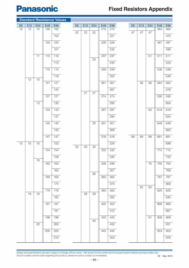
Design and specifications are each subject to change without notice. Ask factory for the current technical specifications before purchase and/or use.
Should a safety concern arise regarding this product, please be sure to contact us immediately.
Fixed Resistors Appendix
– 85 –
Standard Resistance Values
E6 E12 E24 E48 E96
10 10 10 100 100
102
105 105
107
11 110 110
113
115 115
11812 12
121 121
124
127 127
13 130
133 133
137
140 140
143
147 147
15 15 15 150
154 154
15816
162 162
165
169 169
174
178 17818 18
182
187 187
191
196 196
20 200
205 205
210
E6 E12 E24 E48 E96
215 21522 22 22
221
226 226
232
237 23724
243
249 249
255
261 261
26727 27
274 274
280
287 287
294
30 301 301
309
316 316
32433 33 33
332 332
340
348 348
35736
365 365
374
383 38339 39
392
402 402
412
422 42243
432
442 442
453
E6 E12 E24 E48 E96
464 46447 47 47
475
487 487
499
51 511 511
523
536 536
549
56 56 562 562
576
590 590
604
62 619 619
634
649 649
665
68 68 68 681 681
698
715 715
732
75 750 750
768
787 787
80682 82
825 825
845
866 866
887
91 909 909
931
953 953
976
Sep. 201402

● Please contact ● Factory
1. The electronic components contained in this catalog are designed and produced for use in home electric appliances, office equipment, information equipment, communications equipment, and other general purpose electronic devices.
Before use of any of these components for equipment that requires a high degree of safety, such as medical instruments, aerospace equipment, disaster-prevention equipment, security equipment, vehicles (automobile, train, vessel),
please be sure to contact our sales representative.2. When applying one of these components for equipment requiring a high degree of safety, no matter what sort of application it might be, be sure to install a protective
circuit or redundancy arrangement to enhance the safety of your equipment. In addition, please carry out the safety test on your own responsibility.3. When using our products, no matter what sort of equipment they might be used for, be sure to make a written agreement on the specifications with us in advance. 4. Technical information contained in this catalog is intended to convey examples of typical performances and/or applications and is not intended to make any
warranty with respect to the intellectual property rights or any other related rights of our company or any third parties nor grant any license under such rights. 5. In order to export products in this catalog, the exporter may be subject to the export license requirement under the Foreign Exchange and Foreign Trade Law of
Japan.6. No ozone-depleting substances (ODSs) under the Montreal Protocol are used in the manufacturing processes of Automotive & Industrial Systems Company, Panasonic
Corporation.
CAUTION AND WARNING
The information in this catalog is valid as of March. 2018.
Device Solutions Business DivisionAutomotive & Industrial Systems Company Panasonic Corporation1006 Kadoma, Kadoma City, Osaka 571-8506, JAPAN