Embed Size (px)
Citation preview

C ATALOG 2015

INTRODUCTION AbOUT LAYERTEC 2
12
26
42
62
54
50
3
14
31
44
64
56
52
4
16
32
46
66
58
5
18
33
48
68
60
6
19
8
20
22
HOw TO spECIfY sUbsTRATEs
COmpONENTs fOR f2 LAsERs
COmpONENTs fOR Nd :YAG/Nd :YVO4 LAsERs
OpTICAL INTERfERENCE COATINGs
pRECIsION OpTICs
sTANDARD qUALITY sUbsTRATEs
COmpONENTs fOR Arf LAsERs
COmpONENTs fOR THE sECOND HARmONIC Of Nd:YAG, Yb:YAG LAsERs
mETALLIC COATINGs
spUTTERING
AspHEREs, Off AxIs AND fREE fORm OpTICs
COmpONENTs fOR Krf, xeCl AND xef LAsERs
COmpONENTs fOR THE THIRD HARmONIC Of Nd:YAG, Yb:YAG LAsERs
mETAL-DIELECTRIC COATINGs
THERmAL AND E-bEAm EVApORATION
spECIAL OpTICAL COmpONENTs
COmpONENTs fOR RUbY AND ALExANDRITE LAsERs
COmpONENTs fOR THE HIGHER HARmONICs Of Nd:YAG, Yb:YAG LAsERs
mEAsUREmENT TOOLs fOR COATINGs
mEAsUREmENT TOOLs fOR pRECIsION OpTICs
sUbsTRATE mATERIALs fOR UV, VIs AND NIR/IR OpTICs
COmpONENTs fOR Ti : sAppHIRE LAsERs IN THE ns REGImE
COmpONENTs fOR wEAK Nd :YAG/Nd :YVO4 LAsER LINEs
mEAsUREmENT TOOLs fOR COATINGs
TRANsmIssION CURVEs
COmpONENTs fOR DIODE LAsERs
COmpONENTs fOR Ho:YAG AND Tm:YAG LAsERs
mEAsUREmENT TOOLs fOR pRECIsION OpTICs
COmpONENTs fOR Yb :YAG, Yb : KGw AND Yb - DOpED fIbER LAsERs
COmpONENTs fOR Er :YAG LAsERs AND THE 3µm REGION
pRECIsION OpTICs
OpTICAL COATINGs
sELECTION Of OpTICAL COmpONENTs fOR COmmON LAsER TYpEs
COnTenTs
INTRODUCTION PRECISION OPTICS OPTICAL COATINGS SELECTION OF OPTICAL COMPONENTS FOR COMMON LASER TYPES

FEMTOSECOND LASER OPTICS
STANDARD FEMTOSECOND LASER OPTICS
INTRODuCTION TO FEMTOSECOND LASER OPTICS
74
72
92
102
120
114
80
94
108
122
116
84
96
110
124
86
98
112
128
88
90
COMPONENTS FOR ThE ThIRD hARMONIC OF ThE Ti :SAPPhIRE LASER
COMPONENTS FOR OPTICAL PARAMETRIC OSCILLATORS (OPO)
FRONT SuRFACE ALuMINuM MIRRORS
BROADBAND FEMTOSECOND LASER OPTICS
COMPONENTS FOR ThE hIghER hARMONICS OF ThE Ti :SAPPhIRE LASER
BROADBAND AND SCANNINg MIRRORS
SPECIAL METALLIC COATINgS
OCTAVE SPANNINg FEMTOSECOND LASER OPTICS
gIRES -TOuRNOIS - INTERFEROMETER (gTI) MIRRORS
FILTERS FOR LASER APPLICATIONS
SILVER MIRRORS FOR FEMTOSECOND LASERS
OPTICS FOR FEMTOSECOND LASERS IN ThE 1100 –1600nm wAVELENgTh RANgE
ThIN FILM POLARIzERS
hIgh POwER FEMTOSECOND LASER OPTICS
LOw LOSS OPTICAL COMPONENTS
COMPONENTS FOR ThE SECOND hARMONIC OF ThE Ti :SAPPhIRE LASER
COATINgS ON CRySTAL OPTICS
FRONT SuRFACE SILVER MIRRORS
SELECTED SPECIAL COMPONENTS
CLEANINg OF OPTICAL SuRFACES
REgISTER
METALLIC COATINgS FOR LASER AND ASTRONOMICAL APPLICATIONS
126
FEMTOSECOND LASER OPTICS SELECTED SPECIAL COMPONENTS METALLIC COATINGS FOR LASER AND ASTRONOMICAL APPLICATIONS

11
FEMTOSECOND LASER OPTICS SELECTED SPECIAL COMPONENTS METALLIC COATINGS FOR LASER AND ASTRONOMICAL APPLICATIONS
PRECISION OPTICS

12
Price and quality of substrates are determined by material, shape, size, tolerances and polishing quality.
MATERiAL
The first decision is the material of the substrate. It should be free of absorption for all wavelengths of high transmission. If no transmission occurs, a low cost material can be used, e.g. Borofloat® (SCHOTT AG), for metallic mirrors. With respect to the surface form tolerance, a low thermal expansion is beneficial.
SHAPE
The shape must be specified for both sides sepa-rately. Basically all combinations of plane, convex and concave surfaces are possible. A special role plays the wedge. A wedge (e.g. 30 arcmin) can be applied to any kind of surface (plane as well as con-vex or concave). For curved substrates there are different conven-tions for the sign of the radius. Sometimes “+” means convex and “-” means concave. Other users refer “+” and “-” to the light propagation. In this case, “+” means “curvature with the direction of propagation” and “-” means “curvature against the direction of propagation”. Please specify concave or convex in words or by the acronyms CC or CX to avoid confusion.
SizE
The main decision should be about the size, i.e. the edge length or diameter. Small diameters are more favorable for the production. The sagitta heights become lower and it is easier to achieve a good form tolerance.
Although often specified otherwise in optical designs, the thickness description means the maximum thick-ness of the substrate, i.e. the center thickness for plano-convex substrates and the edge thickness for plano-concave substrates. Consequently, the thickness of a wedged plate is measured on the thicker side.
In order to achieve a good form tolerance one should consider the ratio of diameter and thick-ness. As a rule of thumb the thickness should be the fifth of the diameter. Of course, other ratios are possible but the production cost and therefore the price increases.
ToLERAnCES
Besides size and material, the tolerances are most important for manufacturing costs and therefore also for the price. Of course, the optics must fit into the mount, so that the diameter should not be larger than specified. The most common specifica-tion is + 0 - 0.1 mm. Mostly, the thickness is free in both directions. LAYERTEC usually specifies it with a tolerance of ± 0.1 mm. There is a lot of confusion about the specification of wedge, parallelism and centering. Please note that
wedge and parallelism describe the angle between the optical surfaces while centering describes the angle between the optical surfaces and the side surfaces (see fig. 2).
LAYERTEC standard substrates have a parallelism better than 5 arcmin. Specially made parallels may have a parallelism as low as < 10 arcsec. Stand-ard wedged substrates have wedges of 0.5° or 1°. Larger wedge angles are possible depending on the substrate size. Normally, the 90° angle to the side surface has a precision of 20 arcmin. Centering is an additional optics processing step which improves this accuracy to a few arcmin.Using the same nomenclature, one can describe curved substrates. It should be distinguished between mirrors and lenses. The side surfaces of mirror substrates are just parallel. Nevertheless, the direction of the optical axis can be inclined to the side surfaces. After centering, the side surfaces are parallel to the optical axis. In that way, the mirror substrate becomes a lens.
INTRODUCTION PRECISION OPTICS OPTICAL COATINGS SELECTION OF OPTICAL COMPONENTS FOR COMMON LASER TYPES
figure 2: Different kinds of plane substrates with respect to wedge and centering (schematic drawing)
figure 1: Conventions for the specification of the thickness of dif-ferent types of substrates (schematic drawing)
hOw TO SPECIfY SUBSTRATES
planewedge plano-concave
plano-convex
concave-convex
centred substrate
bad substrate
wedged substrate
parallel substrate

13
FEMTOSECOND LASER OPTICS SELECTED SPECIAL COMPONENTS METALLIC COATINGS FOR LASER AND ASTRONOMICAL APPLICATIONS
SuRfACE foRM ToLERAnCE
The surface form tolerance is normally measured by interferometers and is specified in terms of lambda, which is the reference wavelength (λ = 546 nm if not otherwise stated). To avoid confusion, one must clearly distinguish between flatness, power and irregularity. In the following, flatness and irregu-larity shall be explained for a plane surface. Gen-erally speaking, every real surface is more or less curved. Imagine that the “peaks” and “valleys” of a real surface are covered by parallel planes (see fig. 3). The distance between these planes is called the flatness. This flatness consists of two contribu-tions. The first contribution is a spherical bend of the surface, which may be described by two best fitted spheres for the “peaks” and “valleys”. With respect to an ideal plane, the sagitta of this curva-ture is denoted as power. This spherical bend does not affect the quality of the reflected beam. It just causes a finite focal length. The second contribution is the deviation of the best fitted spheres, which is named irregularity. This is the most important value for the quality of the beam.
The standard ISO 10110 provides a sufficient oppor-tunity for specifying the surface form tolerance. Having the best comparability with the measure-ment results, all values are specified as numbers of interference fringes. They should be read as 1 fringe = λ / 2. In the drawings, the surface form tolerance is allocated as item number three: 3 / power (irregularity)Example: A slightly bent (λ / 4) optics which is regu-lar (λ / 10) would be specified as follows: 3 / 0.5 (0.2) Using the optics only for transmission (e.g. laser windows), the power as well as the irregularity do not matter. An uprightly transmitted beam is not affected if the optics has the same thickness all over the free aperture. The deviation from this equality is defined in a similar way as the flatness. It is also measured in parts of the reference wavelength and called “transmitted wave front”. For instance, the window in fig. 3c has a flatness of λ /4 but a trans-mitted wave front of λ /10.
CoATing STRESS
Thin substrates cannot withstand the coating stress. The coating will cause a spherical deformation. This means that a finite sagitta or power occurs. In case of circular substrates, the irregularity is not affected by this issue.The flatness becomes poor when seriously consider-ing the mentioned values. Nevertheless, the quality of a normally incident beam is not affected.
dEfECTS
MIL-O-13830 and ISO 10110 are different standards for the description of optical elements. This often causes obscurities. Basically, one should distinguish between scratches and digs. The scratch number
in MIL-O-13830 means the visibility of the biggest scratch compared to the corresponding one on a norm template. Actually “10” is the smallest scratch on this template. Thus, better qualities cannot be specified seriously. The MIL norm does not specify a directly measured scratch width. Sometimes the number is interpreted as tenths of a micron, some-times as microns. Actually, a direct measurement never corresponds to the MIL norm. In contrast to the scratch, the dig number can be measured easily. The numerical value means the maximum dig diameter in hundredths of a millimeter. Maximum size digs can be one per 20 mm of diam-eter. According to ISO 10110 the defects are speci-fied as item number 5. The grade number means the side length in millimeters of a quadratic area which is equivalent to the total fault area. So, 5 / 1 x 0.025 means a surface fault area of 0.000625 mm². Addi-tionally, scratches of any length are denoted with a leading L. A long scratch with a width of 4 microns would be specified as L 1 x 0.004.All these explanations are very simplified. For a detailed specification please read the complete text of the relevant standard.
PLEASE noTE:
There is no direct conversion between MIL-O-13830 and ISO 10110. All specifications in this catalog cor-respond to ISO 10110. The mentioned scratch/dig values are a rough analog to MIL-O-13830.
figure 3: Schematic drawing for the explanation of substrate properties: a) Flatness of λ /10 b) Spherical bending (power of λ /4) c) Irregularity of λ /4, but transmitted wavefront of λ /10
a) Flatness
λ /10
c) Irregularity
λ /4
b) Power
λ /10
λ /4

14
Plane substrates, parallels and wedges• Standard plane substrates: wedge < 5 arcmin • Standard parallels: wedge < 1 arcmin or wedge < 10 arcsec• Standard wedges: wedge = 30 arcmin or wedge = 1 deg
Plano- concave and plano- convex substrates• Standard radii: 25, 30, 38, 50, 75, 100, 150, 200, 250, 300,
400, 500, 600, 750, 1000, 2000, 3000, 4000, 5000 mm
dimensions• Fused silica, ULE®, Zerodur®, N-BK7®: diameter 6.35 mm … 508 mm (¼ inch … 20 inches)• Calcium fluoride, YAG, sapphire: diameter 6.35 mm … 50.8 mm (¼ inch … 2 inches)• Rectangular substrates and other diameters avail-
able on request
Tolerances• Diameter: + 0 mm, - 0.1 mm• Thickness: ± 0.1 mm• Clear aperture: central 85 % of dimension• Chamfer: 0.2 … 0.4 mm at 45°
The precision optics facility of LAYERTEC produces plane and spherical curved mirror substrates, lenses and prisms of fused silica, optical glasses like N-BK7® and SF14® and some crystalline materials, e.g. cal-cium fluoride and YAG. In the following you can find information on the specifications of our standard substrates. Please do not hesitate to contact us also for other sizes, shapes, radii and materials or for special com-ponents.
STANdARd QUALITY SUBSTRATES
INTRODUCTION PRECISION OPTICS OPTICAL COATINGS SELECTION OF OPTICAL COMPONENTS FOR COMMON LASER TYPES
materials • Fused silica: Corning 7980® or equivalent• Fused silica for high power applications: Suprasil® 300 / 3001 / 3002 or equivalent• UV fused silica (excimer grade): SQ1 E-193® and SQ1 E-248®
• IR fused silica: Infrasil 302® or equivalent• ULE®
• Zerodur®
• N-BK7® or equivalent• CaF
2:
single crystal, random oriented, special orien-tations on request, excimer grade (248 nm and 193 nm) on request
• Sapphire: single crystal, random oriented, special orienta-
tions on request• YAG: undoped, single crystal, random oriented
All trademarks mentioned are the property of the respective owners.
STAndARd SPECifiCATionS
tc
r
te
r
tt
tc
r
te
r
tttc
r
te
r
tt
tc
r
te
r
tttc
r
te
r
tt
tc
r
te
r
tt
Ø: Diameter [mm]t
e: Edge thickness [mm]
tc: Center thickness [mm]
t: Thickness [mm]

15
FEMTOSECOND LASER OPTICS SELECTED SPECIAL COMPONENTS METALLIC COATINGS FOR LASER AND ASTRONOMICAL APPLICATIONS
Material Standard Specification on request
Fused silica planespherical
λ / 10λ / 4 reg. (typical λ / 10 reg.)
λ / 30λ / 30 reg. (Ø < 51 mm)
ULE® and Zerodur® planespherical
λ / 10λ / 4 (typical λ / 10 reg.)
λ / 30λ / 30 reg. (Ø < 51 mm)
N-BK7® planespherical
λ / 10λ / 4 reg. (typical λ / 10 reg.)
λ / 30λ / 30 reg. (Ø < 51 mm)
CaF2 plane Ø < 26 mm
plane Ø < 51 mmspherical
λ / 10λ / 4λ / 4 reg.
λ / 20λ / 20λ / 20 reg.
Sapphire λ / 2 λ / 30
YAG planespherical
λ / 10λ / 4 reg. (typical λ / 10 reg.)
λ / 30λ / 30 reg. (Ø < 51 mm)
Si planespherical
λ / 10λ / 4 reg. (typical λ / 10 reg.)
λ / 20λ / 20 reg. (Ø < 51 mm)
Surface form tolerance (reference wavelength: 633nm)
Material Standard Roughness
Standard Specification on request
Fused silica < 2 Å 5 / 1 x 0.025 L1 x 0.001 Scratch-Dig 10-3
< 1.2 Å 5 / 1 x 0.010 L1 x 0.0005 Scratch-Dig 5-1
ULE® < 2 Å 5 / 3 x 0.025 L1 x 0.001 Scratch-Dig 10-5
< 2 Å 5 / 1 x 0.010 L1 x 0.0005 Scratch-Dig 5-1
Zerodur® < 4 Å 5 / 2 x 0.040 L1 x 0.001 Scratch-Dig 10-5
< 3 Å 5 / 2 x 0.025 L1 x 0.0010 Scratch-Dig 10-3
N-BK7® < 3 Å 5 / 2 x 0.040 L1 x 0.001 Scratch-Dig 10-5
< 3 Å 5 / 2 x 0.025 L1 x 0.0010 Scratch-Dig 10-3
CaF2 < 4 Å 5 / 3 x 0.025 L1 x 0.0025
Scratch-Dig 20-3< 1.5 Å 5 / 3 x 0.016 L1 x 0.0010
Scratch-Dig 10-2
Sapphire < 5 Å 5 / 3 x 0.025 L20 x 0.0025 Scratch-Dig 20-3
< 3 Å 5 / 3 x 0.016 L1 x 0.0010 Scratch-Dig 10-2
YAG < 3 Å 5 / 1 x 0.025 L2 x 0.0025 Scratch-Dig 20-3
< 3 Å 5 / 1 x 0.010 L1 x 0.0005 Scratch-Dig 5-1
Si < 3 Å 5 / 3 x 0.025 L1 x 0.001 Scratch-Dig 10-5
< 2 Å 5 / 1 x 0.010 L3 x 0.0005 Scratch-Dig 5-1
Surface quality
All specifications according to ISO 10110 (Ø 25 mm). The mentioned Scratch-Dig values are approximately equivalent to MIL-O-13830

16
ASPhERES, Off-AXIS ANd fREE fORm OPTICS
INTRODUCTION PRECISION OPTICS OPTICAL COATINGS SELECTION OF OPTICAL COMPONENTS FOR COMMON LASER TYPES
Plane and spherical optics can be efficiently manu-factured by using traditional techniques of area grinding and polishing. The tool always works on a significant fraction of the substrate area at once. It is not or hardly possible to manufacture surface geometries that differ from regular forms like planes, spheres or cylinders.
Using ultra precision CNC machinery, surfaces can be zonally processed, i.e. the tool works on one point at a time. The possible surface forms and tolerances are only limited by the precision of the machine and the measurement equipment. In contrast to the areal techniques, zonal processing usually works with one single piece per run only.
The non-spherical optics can be divided in three groups: rotational symmetric non-spherical, off-axis and free form optics.
The focal length of the parent parabola (parent focal length) is measured from the vertex on the optical axis. For the off-axis parabola, an effective focal length f
eff is introduced.
The off-axis distance is measured from the optical axis to the middle of the OAP. The radius R denotes the radius of curvature in the vertex of the parent parabola. The conic constant k is -1.
Neglecting the aspheric coefficients leads to a profile of conic sections:• Ellipse: -1 < k < 0• Sphere: k = 0• Parabola: k = -1
An off-axis surface can be seen as a section of a bigger on-axis surface. The focal point still is on the original optical axis but not the center of the section. It is located off axis.
Off-axis surfaces derived from aspheres are described by the mentioned equation, the off-axis distance a and / or the off-axis angle α.
Examples:• Off-axis parabolas• Off-axis ellipses• Off-axis hyperbolas• Off-axis spheres• Off-axis cylinders
BASiCS RoTATionAL SYMMETRiC non SPHERiCALoPTiCS (ASPHERES) off-AXiS SuRfACES
dimension Tolerances
Total diameter 25 … 560 mm < 0.1 mm
inspection range < 550 mm
Total thickness < 100 mm < 0.1 mm
displacement < 50 mm
Centering error < 50 μm
Tilting error < 30 ''
Surface formtolerance
< λ / 4 (< λ / 10 on request)
Roughness < 3 Å
Table 1: Production dimensions and tolerances
figure 2: Profile of an aspheric mirror
figure 3: Schematic drawing of an off-axis parabolafigure 1: Aspheric lens
z = displacementk = conic constantr = distance from axisR = radius of curvatureA
i = aspheric coefficients
z (r) =R 1 + 1 – (1 + k)
r2
+ A4 r4 + A
6 r6 + …
r2
R2
Although the term “asphere” may stand for any non-spherical optics, it is often referenced to rotationally symmetric non-spherical optics. They are described by the following equation (ISO 10110):
Example: off-Axis Parabola (oAP)
z
r
total diameteropening diameterinspection range
centering errortilting error
cent
erth
ickn
ess
sagi
tta
heig
ht
tota
l thi
ckne
ss
z
ra
f-pa
rent
f-eff
Ø
α

17
FEMTOSECOND LASER OPTICS SELECTED SPECIAL COMPONENTS METALLIC COATINGS FOR LASER AND ASTRONOMICAL APPLICATIONS
In principle an off-axis substrate can always be mechanically cut from an on-axis substrate. The alternative way is a direct manufacturing. Depending on the size and tolerances, both ways are possible. Fig. 4 shows the common process of manufacturing a number of smaller OAPs from a parent parabola.
Free form surfaces are always customer specific, defined by a number of points or equations. No symmetry may be assumed. Free form surfaces are manufactured as single pieces.Table 2 shows LAYERTEC’s production dimensions and tolerances for free form surfaces.
The surface quality and the final tolerances depend very strongly on the material of the substrate. LAYERTEC has an optimized process for fused silica. Materials like Zerodur®, ULE® or N-BK7® may be used in special cases.
Measuring aspheric surfaces requires sophisticated devices. LAYERTEC applies 4 different measurement principles.
• Tactile measuring The tip has mechanical contact to the surface and
its excursion is recorded. It measures one line at a time. Precision < 200 nm on a 200 mm line.
• Single point interferometer Contactless measurement of the surface, measur-
ing the surface point by point. Precision < 50 nm on a diameter of 420 mm.
• interferometer with reference surface It compares the surface to a well-known reference
surface. Precision < 50 nm, diameter 300 mm. Concave surfaces preferred.• interferometer with hologram It compares the surface to the wave front which is
generated by a computer generated hologram (CGH).
fREE foRM SuRfACES MATERiALS
MEASuREMEnT
Table 2: Dimensions and tolerances of free form substrates
figure 6: Schematic drawing of an off axis ellipses
figure 4: Manufacturing off-axis parabolas as pieces of one "parent parabola"
figure 5: Basic properties of a free form substrate
figure 6: LuphoScan single point interferometer
dimension Tolerances
Ø < 300 mm 0.2 mm
b < 300 mm 0.1 mm
c < 450 mm 0.1 mm
α < 45°
t < 80 mm 0.1 mm
a
Surface formtolerance
< λ / 2 (λ / 4 on request)
Roughness < 3 Å
a
d ± 0.1 mm
Ø /2opening diamete
r
t ± 0
.1 m
m
d M±
0.2
mm
b ±
0.1
mm
c ± 0.1 mm
a = off-axis distanceb = widthc = lengtht = thicknessα = off-axis angled = distance between center beam and reference edge
α
α
z
r
Off-Axis
Parent parabola
A A
a ± 0.1 mm
Ø ± 0.1 mm
d ±
0.2
mm

18
As a kind of a Fabry-Pérot interferometer, the etalon is typically made of a transparent plate with two reflective surfaces. Its transmission spectrum, as a function of wavelength, exhibits peaks of high transmission corresponding to resonances of the etalon. Etalons are widely used in telecommunica-tion, lasers and spectroscopy for controlling and measuring the wavelength of laser sources.
LAYERTEC offers etalons of customized diameters and various materials depending on the wavelength range. Thicknesses down to 50 μm and a parallel-ism < 1 arcsec are possible subject to the diameter. Do not hesitate to contact us for the customized diameter and thickness you need.
SPECIAL OPTICAL COmPONENTS
INTRODUCTION PRECISION OPTICS OPTICAL COATINGS SELECTION OF OPTICAL COMPONENTS FOR COMMON LASER TYPES
ThicknessParallelism
Ø = 50 mm Ø = 25 mm Ø = 12.7 mm
fused Silica ≥ 200 μm ≥ 130 μm ≥ 50 μm < 1 arcsec
YAg ≥ 200 μm ≥ 130 μm ≥ 50 μm < 1 arcsec
Caf2
–––– ≥ 300 μm ≥ 100 μm < 5 arcsec
order Ø = 38 mm Ø = 25 mm Ø = 12.7 mm Precision Parallelism
λ / 2 Available wavelengths
K = 0 ––– ––– λ = 900 nm ± 1 μm < 1 arcsec
K = 1 λ = 900 nm λ = 800 nm λ = 350 nm ± 1 μm < 1 arcsec
K = 2 λ = 550 nm λ = 500 nm λ = 300 nm ± 1 μm < 1 arcsec
λ / 4 Available wavelengths
K = 1 λ = 1060 nm λ = 940 nm λ = 400 nm ± 1 μm < 1 arcsec
K = 2 λ = 620 nm λ = 530 nm λ = 300 nm ± 1 μm < 1 arcsec
CuSToMizEd PRiSMS And SHAPES
In addition to the mentioned circular substrates, LAYERTEC is able to produce a lot of different shapes. Uncommon optics are possible besides rectangular substrates, wedges and prisms. Typical examples of uncommon optics are defined holes through the optics. So-called D-cuts and notches can be produced.
PoLiSHing of CRYSTALS
Besides the high quality optical coatings on crystals (see pages 116, 117), LAYERTEC supports the polish-ing of various types of crystals such as YAG, KGW, KYW, ZGP or LBO. Our polishing technology also enables the careful handling and processing of small crystal sizes or extraordinary forms. Do not hesitate to contact us for your special problem.
ETALonS
wAVEPLATES
LAYERTEC has established a production line for plane and spherical optics up to a diameter of 500 mm. This also includes interferometers. Mea-surements for large optics are described on page 22. The optics can be coated using magnetron sputtering and IAD. The main products are large scale laser mirrors. A coating uniformity of ± 0.5 % was demonstrated which also enables the produc-tion of large scale thin film polarizers and other complex coating designs.
LARgE SCALE oPTiCS
figure 1: Mirror substrate with a diameter of 500 mm
LAYERTEC offers customer specific retardation plates made of crystalline quartz. due to the mini-mal required thickness the below mentioned wave plates are available:

19
SUBSTRATE mATERIALS fOR Uv, vIS ANd NIR/IR OPTICS
FEMTOSECOND LASER OPTICS SELECTED SPECIAL COMPONENTS METALLIC COATINGS FOR LASER AND ASTRONOMICAL APPLICATIONS
YAg (undoped)
Sapphire Baf2
Caf2
infrasil®1) fused silica(uV) n-BK7®2) Sf10®2)
wavelength range free of absorption
400 nm – 4 µm
400 nm – 4 µm
400 nm – 10 µm
130 nm – 7 µm
300 nm – 3 µm
190 nm – 2.0 µm3)
400 nm – 1.8 µm
400 nm – 2.0 µm
Refractive index at
200 nm 1.49516 1.55051
300 nm 1.45403 1.48779
500 nm 1.8450 1.775 1.479 1.43648 1.46233 1.46243 1.5214 1.7432
1 µm 1.8197 1.756 1.468 1.42888 1.45042 1.45051 1.5075 1.7039
3 µm 1.7855 1.71 1.461 1.41785 1.41941
5 µm 1.624 1.451 1.39896
9 µm 1.408 1.32677
Absorbing in the 3 µm region no no no no yes yes yes yes
Absorbing in the 940 nm region For high power applications at 940 nm we recommend the fused silica types SuPRASIL 300®1) and SuPRASIL 3001/3002®1)
Birefringence no yes no no4) no no no no
Thermal expansion coefficient[10–6K] 5)
7 5 19 18 0.5 0.5 7 8
Resistance against temperature gradients and thermal shock
high high very low low high high medium medium
gdd fs² per mm
400 nm 240 150 90 68 98 98 120 640
800 nm 97 58 38 28 36 36 45 160
1064 nm 61 29 26 17 16 16 22 100
1500 nm 13 -25 13 1.9 -22 -22 -19 38
2000 nm -59 -120 -2.4 -21 -100 -100 -99 -36
Tod fs3 per mm
400 nm 75 47 27 19 30 30 41 500
800 nm 57 42 20 16 27 27 32 100
1064 nm 71 65 22 21 44 44 49 100
1500 nm 140 180 34 46 130 130 140 140
2000 nm 360 530 72 120 450 450 460 350
1) Registered trademark of Heraeus Quarzglas GmbH & Co. KG2) Registered trademark of SCHOTT AG3) Absorption band within this wavelength range, please see transmission curve4) Measurable effects only in the VUV wavelength range
5) The values given here are rounded, because the measurements of different authors in the literature are inconsistent.
Please note that the thermal expansion coefficient of crystals depends also on the crystal orientation.
All values are for informational purposes only. LAYERTEC cannot guarantee the correctness of the values given.
20
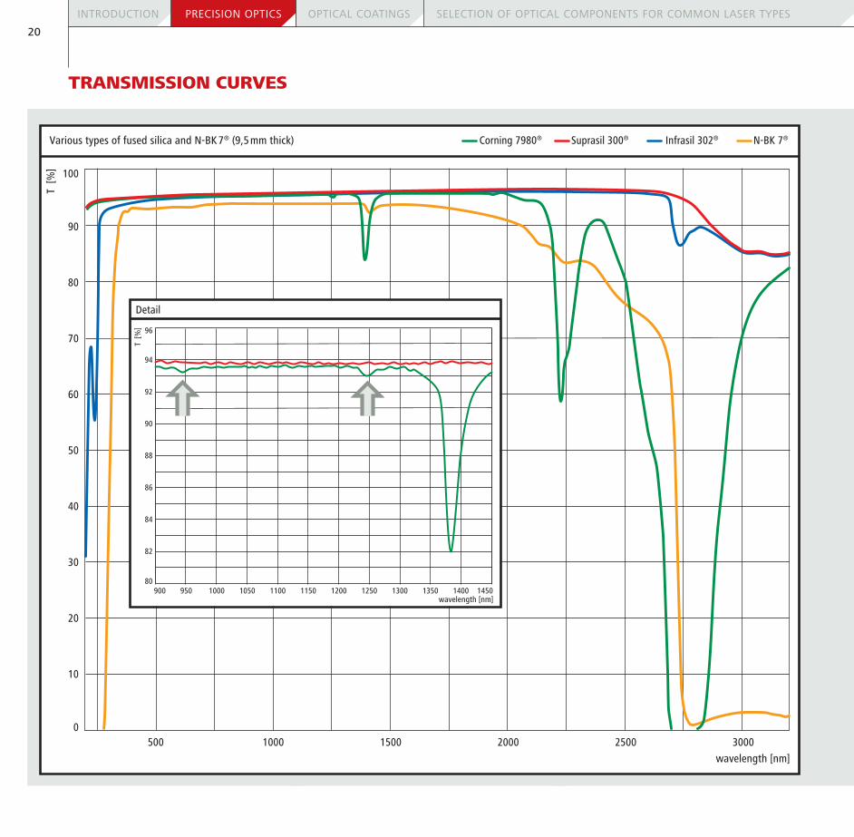
TRANSmISSION CURvES
INTRODUCTION PRECISION OPTICS OPTICAL COATINGS SELECTION OF OPTICAL COMPONENTS FOR COMMON LASER TYPES
Various types of fused silica and N-BK7® (9,5mm thick)
wavelength [nm]
T [%
]
20
60
100
80
40
01500 2500
70
50
30
10
1000 2000 3000500
90
Corning 7980® Suprasil 300® Infrasil 302® N-BK 7®
84
92
96
88
80
94
90
82
T [%
]
86
950900 1250 1300 145010501000 1100 1150 1200 1350 1400wavelength [nm]
Detail

21
FEMTOSECOND LASER OPTICS SELECTED SPECIAL COMPONENTS METALLIC COATINGS FOR LASER AND ASTRONOMICAL APPLICATIONS
YAG undoped (3mm thick) Sapphire (3mm thick)
Calcium fluoride (3mm thick)
wavelength [nm] wavelength [nm]
wavelength [nm] wavelength [nm]
200 3200 6200
20
40
60
80
100
0
T [%
]
1200 4200 52002200 300 3300 6300
20
40
60
80
100
0
T [%
]
1300 4300 53002300
5300120 10300
20
40
60
80
100
0
T [%
]
180 6300 8300240 123007300 9300 11300300
Barium fluoride (3mm thick)
20
40
60
80
100
0
T [%
]
190 4200 10200390 6200 82002200 12200 14200 16200

22
For the measurement of surface form and regularity, the precision optics facility of LAYERTEC is equipped with laser interferometers and special interferometer setups for plane, spherical and parabolic surfaces. Additionally, a tactile measurement device (Taylor Hobson PGI 1240 Asphere) is available for general aspheric and grinded surfaces. Besides the purpose of quality control, surface form measurement is a key function for the zonal polishing technology established at LAYERTEC.
Abbreviations• P-V: The peak-to valley height difference• RoC: Radius of curvature of a spherically curved
surface.• : measuring wavelength of the laser interfer-
ometer (e.g. 633 nm or 546 nm). The P-V value is stated in a fractional amount of λ. The concrete value of λ is stated in our protocols.
For detailed information about the standards con-cerning surface form measurement please refer to ISO 10110-5.
Accuracy of interferometric measurementsWithout special calibration procedures, the accu-racy of an interferometric measurement is only as accurate as the reference surface. Calibration can increase the accuracy by a factor of 2 or more. Furthermore, the precision is influenced by the size of the measured area and in case of a curved surface by the radius of curvature itself. The accuracy values stated as “P-V better than …” in the following articles are guaranteed values. Very often accuracies of λ / 20 or better will be achieved.
Standard measurementsIn general, the form tolerance of spherical and plane optics with diameters Ø ≤ 100 mm can be measured with an accuracy of P-V better than λ / 10 by using
ZYGO Fizeau interferometers. To cover a measure-ment range of ROC = ± 1200 mm over an aperture of Ø = 100 mm, LAYERTEC uses high precision JenFIZAR Fizeau objectives. In many cases, a higher accuracy up to P-V = λ / 30 is possible. Measurement protocols can be provided on request.
Large Radius Test (LRT)Surfaces with radii of curvature beyond ± 1200 mm are tested with a special Fizeau zoom lens setup called Large Radius Test (LRT). This setup was developed by DIOPTIC GmbH in cooperation with LAYERTEC.Its operating range is ROC = ± 1000 mm … ± 20.000 mm at working distances lower than 500 mm. The accuracy is guaranteed as P-V = λ / 8 over Ø ≤ 100 mm, but typically it is better than P-V = λ / 15. LRT has the advantages that only one Fizeau-objective is needed to cover a wide range of radii of curvature and that the working distance is kept small. This reduces the influence of disturbing air turbulences during the measurement.
Large aperture interferometryLAYERTEC uses high performance interferometers especially for laser optics with large dimensions. A wavelength-shifting Fizeau interferometer (ADE Phaseshift MiniFIZ 300®) is used for flat surfaces. LAYERTEC has enlarged the measurement aperture of the system with a special stitching setup. The measurement range of the system is:
• P-V up to λ / 50 (633 nm) at Ø ≤ 300 mm with a full aperture measurement
• P-V better than λ / 10 (633 nm) at Ø ≤ 600 mm with a special stitching measurement setup.
Figure 1 shows the height map of a flat surface with diameter of Ø = 520 mm which was measured with the MiniFIZ 300 interferometer and the stitching configuration at LAYERTEC.
The measurements of spherical concave surfaces are made with a Twyman-Green interferometer (Phase-Cam 5030®; 4D-Technology). This interferometer uses a special technology which allows measurement times in the region of a few milliseconds. Therefore, the interferometer is insensitive to vibrational errors when measuring over long distances up to 20 m between the device and the specimen. The measure-ment accuracy of the system is P-V better than λ / 10 at Ø ≤ 600 mm with a full aperture measurement (in case of concave surfaces).
.
mEASUREmENT TOOLS fOR PRECISION OPTICS
INTRODUCTION PRECISION OPTICS OPTICAL COATINGS SELECTION OF OPTICAL COMPONENTS FOR COMMON LASER TYPES
SuRfACE foRM MEASuREMEnT
figure 1: Height map of a flat surface with a diameter of Ø = 520 mm polished and measured at LAYERTEC. The P-V value is λ / 10 over the full aperture (Ø = 500 mm inspection area) after zonal correction.

23
The surface roughness value of an optical surface is denoted as roughness parameter Rq or Sq. This parameter is also named “RMS roughness” because it is calculated as the root mean square of the surface height values. The letter “R” indicates that only a two-dimensional roughness profile is the basis of the calculation according to ISO 4287-1. The letter “S” means a three-dimensional measurement and calculation (3D-Reference ISO 25178-2).
The corresponding measurement device and the spectral range within which the optical surface should be used have to be taken into account when measuring and stating roughness parameters of optical surfaces. The spatial resolution of the roughness measurement device plays an important role with respect to the roughness value. A higher spatial resolution allows the detection of smaller surface structures and higher spatial frequencies. Furthermore, the amount of stray light losses on the surface depends on the spatial frequencies of the surface structures and the wavelength of the light itself. Fig. 2 shows the spatial frequencies which influence the scattering losses in different spectral ranges and typical spatial resolutions of roughness measurement devices.
Generally, for the characterization of optical surfaces which are appointed to be used in the NIR, VIS and UV spectral range, surface roughness measurements should be accomplished with spatial resolutions which are equal or better than 10 / μm to obtain roughness information over the entire relevant spatial frequency range. Fig. 3 clarifies the differ-ences between an AFM measurement and an optical surface profiler measurement with respect to the calculated RMS roughness and the spatial resolution.
FEMTOSECOND LASER OPTICS SELECTED SPECIAL COMPONENTS METALLIC COATINGS FOR LASER AND ASTRONOMICAL APPLICATIONS
* For more information on stray light losses please see: A. Duparré, "Light scattering on thin dielectric films" in "Thin films for optical coatings", eds. R. Hummel and K. Günther, p. 273 – 303, CRC Press, Boca Raton, 1995.
figure 3: Surface roughness measurement of a super polished Low Loss substrate for an UV application made of fused silica. Both images show the same region on the surface, but they were recorded with different measurement devices (optical surface profiler and AFM). The color bar scaling is ± 1 nm for both images. With equivalent lateral pixel scaling, the AFM measurement with high spatial resolution shows fine structures which are relevant for stray light losses. The opti-cal profiler measurement only shows a few pixels but no significant information about the surface roughness and structures. Therefore, undersampling yields better rough-ness values and overstates the surface quality.
figure 2: Spatial frequency resolution of AFM and 3D optical surface profiler at LAYERTEC for typical scan sizes. Additionally, the figure shows the spatial frequency ranges which influence the scattering losses in the VIS and DUV spectral range*.
LAYERTEC has available a phase shifting three-dimen-sional optical surface profiler (Sensofar) and a scan-ning probe microscope (AFM) DI Nanoscope 3100 for the purpose of measuring and analyzing the surface roughness of optical components. The optical profiler provides a low spatial resolution < 2 / μm combined with an acquisition time of only a few seconds. The device is used for the measurement of optics with lower surface roughness requirements and for the general inspection of the polishing processes. Surface defects and inhomogeneities can be characterized too. The AFM is used for the characterization of polished surfaces with roughness values Sq < 0.5 nm. This device has a very high spatial resolution hori-zontally and vertically, but the acquisition time is approximately 10 – 30 minutes. Therefore, it is primarily used for the further development of the polishing processes. Our premium polishing process and especially our optics for UV applications with Sq <0.2nm are checked periodically for quality control reasons. The standard AFM measurement parameters at LAYERTEC are: Scan size of 10 x 10 μm² and a spatial resolution of 25 / μm (see fig. 2). Measure-ment reports are available on request.
SuRfACE RougHnESS MEASuREMEnT
Spatial Frequency [1 / µm]1 10 1000.001 10000.01 0.1
Spatial Resolution Bandwidth
3D optrical surface profiler250 x 250 µm2
AFM 10 x 10 µm2
AFM 1 x 1 µm2
Scattering Losses λ = 193 nm(DUV)
Scattering Losses λ = 633 nm

INTRODUCTION PRECISION OPTICS OPTICAL COATINGS SELECTION OF OPTICAL COMPONENTS FOR COMMON LASER TYPES
24
OPTICAL COATINgS