Embed Size (px)
Citation preview

Carbon Nanotubes by MicrowaveCarbon Nanotubes by MicrowavePlasmaPlasma--Enhanced Chemical Enhanced Chemical
Vapor DepositionVapor Deposition
M. Maschmann2, A. Goyal3, Z. Iqbal3, T.S. Fisher2, R. Gat1
1. Seki Technotron USA. Santa Clara CA, USA. [email protected]. Purdue University, School of Mechanical Engineering and BirckNanotechnology Center3. New Jersey Institute of Technology, Department of Chemistry
pdfMachine by Broadgun Software - a great PDF writer! - a great PDF creator! - http://www.pdfmachine.com http://www.broadgun.com

MWCNT- 100mm wafer� Spin on multiwall
catalyst- no sputtering
� 6nm Fe particles suspended in oil
� Process:� 50% CH4 in H2, � 300 W, � 5 Torr, � 850 C
100 mm

Significance of PECVD
� Plasma dissociates hydrogen/methane mix into reactive radicals mostly atomic hydrogen (H), and methyl (CH3)
� Plasma CVD has shown vertically oriented, dense forests of carbon nanotubes. L. C. Chen, National Taiwan Univ

MWCNT/MWCVD
0
100
200
300
400
500
600
1200 1400 1600 1800
Raman Shift cm^-1
0 cm(edge)
1 cm
2 cm

Motivation� Provide microwave plasma deposition technology to enable:
� Large area 200-300mm� deposition temperature <450C. � Particle and impurity control� Reliable, reproducible� Semiconductor process compatible
� Reduce required growth temperatures for SWCNTs by thermal CVD from 900-1200 oC.
� MICROWAVE Plasma generates radical density characteristic of 2000C at much lower effective temperature e.g < 450C and can be highly ionized (Low pressure ECR mode) or highly neutral (high pressure mode).

Microwave PECVD System1.5kW and 2.5GHz
Microwave Generator
Dual WavelengthPyrometer MeasuresSurface Temperature
Vacuum Chamber
Seki Technotron Corp.AX5200 Series
Process Gasses:H2: 0-1000 sccmCH4: 0-10 sccm
Substrate DC Bias:0 � 600 V; 0 � 1.7 A
3.5 Kilowatt, 900C RFHeating of 4� Substrate
External Interlocksfor Safe Hands-FreeOperation
Embedded K-type thermocouple monitorsstage temperature
Plasma Deposition system
� Microwave plasma
� DC bias
� RF induction heating � water cooled coil
� thermocouple Pump
+ + +
Substrate
� Ellipsometry, IR Pyrometry and laser interferometry

SWCNT Catalyst Synthesis
� Catalyst/support made by sol-gel method: � Mix powders and form �Sol�:
� Magnesium NitrateMg(NO3).6H2O, 0.5g
� Cobalt Nitrate Co(NO3).6H2O, � Ammonium Heptamolybdate
(NH4)6Mo7O24.4H2O,� citric acid, 3g� distilled water
� typically 4:1 Mo:Co supported on MgO:MgO(1-x-y)CoxMoy

Catalyst/support Synthesis
� Solution placed in ceramic boat and loaded into 550 oC furnace for 5 minutes in air
� Resulting bimetallic Mo:Co catalyst and MgOsupport was ground to a fine powder using a mortar and pestle
� 0.030 grams of powder added to 25mL and ultrasonically agitated for 3 hours before being dispersed onto silicon substrates
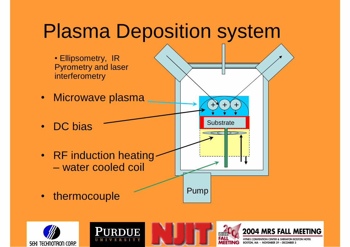
Synthesis Conditions
Catalyst Temperature Pressure Feedstock Gasses PlasmaMo / Co catalyst with 600 - 800 C 10 Torr 10:1 H2 : CH4 200 W
MgO support
Catalyst Temperature Pressure Feedstock Gasses Plasma1 Fe / Co catalyst with
Faujasite-type zeolite 550 - 850 C 0.5 Torr 7 : 4 H2 : CH4 900 Wsupport
Ferratin nanoparticles and2 sub-monolayer e-beam 600 C 0.5 Torr 1 : 4 Ar : CH4 75 W
evaporated iron
Current work
Prior PECVD SWCNT but not MICROWAVE plasma:1) T. Kato et a., Chem. Phys. Lett., 381, 422 (2003).
2) Y. Li et al., Nano Lett., 4, 317 (2004).

SEM � Microns long bundles of SWCNTs

AFM ImageAFM Image

Deposition temperature 800 oC
1000 1200 1400 1600 1800
Raman shift (cm-1)
Inte
nsity
(a.
u.)
1308 1593
Horiba/Jobin Yvon LabRam system with cooled CCD (charge coupled device) detection and 632.8 nm laser excitation with 15 mW intensity at the source and approximately 1.5 mW at the sample
� D (disorder)-band at 1308 cm-1 � High intensity consistent with a:C or poor resonance condition
� G (graphite)-band at 1593 cm-1

Deposition temperature 800 oC
� Radial breathing modes at 189 and 254 cm-1
correspond to 1.3 and 0.9 nm diameter, respectively*
� Based on laser excitation energy and Raman shift, 0.9 nm CNTs are semiconducting while 1.3 nm CNTs are metallic**
100 200 300 400 500
Raman Shift (cm-1)In
tens
ity (
a.u.
)
189
299
254
*S. M. Bachiloet al., Science, 298, 2361 (2002). **H. Kataura et al., Synth. Met., 103, 2555 (1999).

Deposition temperature 600 oC� Weak Radial breathing
modes at 175, 192, 206, and 226 cm-1 corresponding to diameters from 1.2 to 1.5 nm.
� Strong D band likely a:C
7000
8000
9000
10000
11000
12000
13000
14000
15000
100 150 200 250 300
Raman Shift (cm -1)
Inte
nsi
ty (
a.u
.)175
192206
226
1000 1400 1800
Raman Shift (cm-1)
Inte
nsi
ty (
a.u
.)
1305 1591
1160
(b)
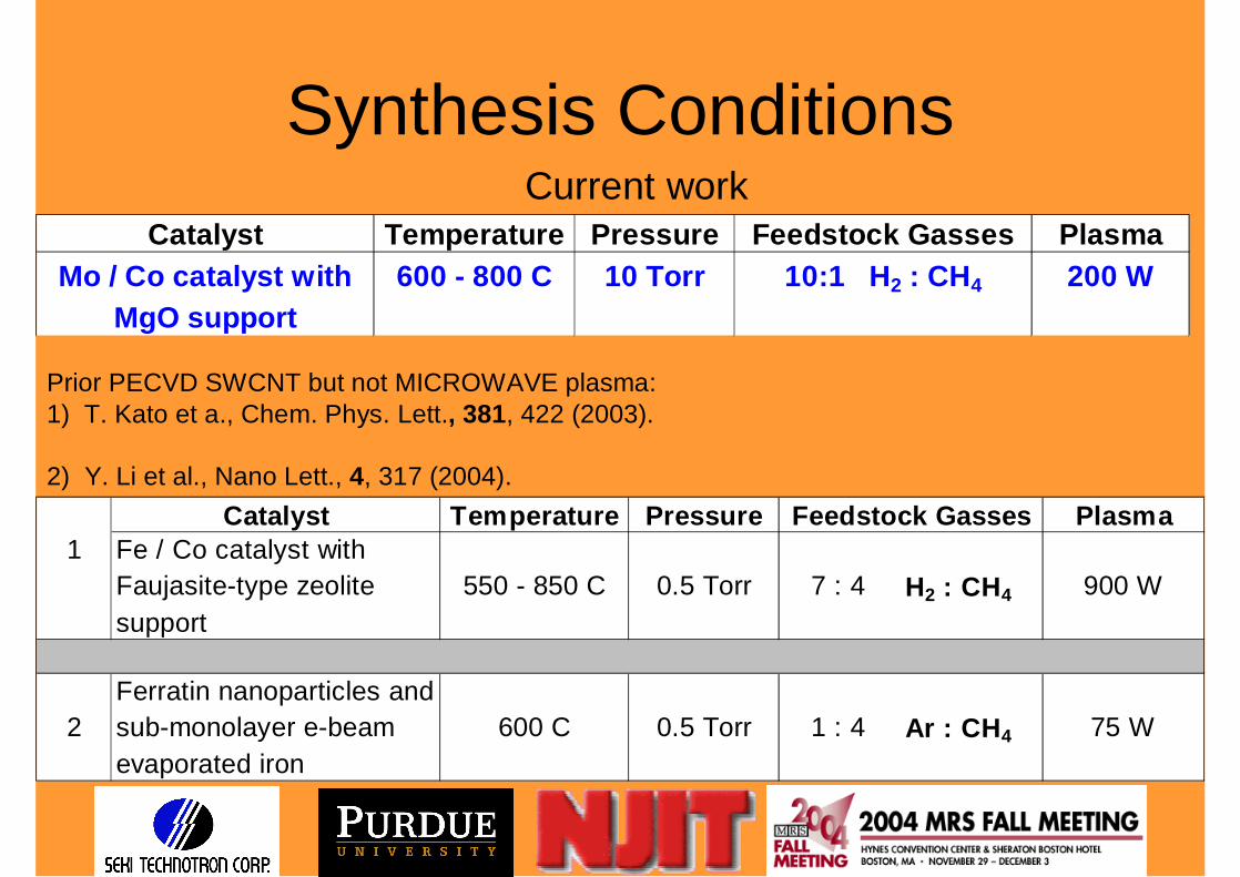
Data: �Diamond 2003�, 14th European Conference on Diamond, Diamond-like Materials, Carbon Nanotubes, Nitrides and Silicon Carbide
MW and SW CNT deposition temp vs. Pressure (multiple sources)
0100200300400500600700800900
1000
0 200 400 600 800
Pressure (Torr)
Su
bst
rate
Tem
p (C
)
Robertson, Cambridge U., UK, DC plasma
Woo, KIST, Korea, ECR-MW
plasma

Electron Cyclotron Resonance ECR
� mTorr Operation� Room
temperature deposition
� High rate� plasma density� radical flux

ECR- CNT Deposition
System

Conclusions� Multiwall and Single wall CNT were
deposited using Sekitechnotron/ASTeX microwave PECVD.
� Deposition area 100mm diameter wafers
� Both semiconducting and metallic SWCNTs were synthesized at 600C and higher temperatures.

Acknowledgements
� NJIT thanks the US Army and NSF
� Purdue thanks NASA-Purdue Institute for Nanoelectronics and Computing and BirckNanotechnology Center
� Sekitechnotron thanks Dr. Tarun Sharda for depositions.