Embed Size (px)
Citation preview

..........................................................................CollectionTechnique
Cahier technique n° 187
Cohabitation of high and lowcurrents
R. CalvasJ. Delaballe
Merlin Gerin Square D Telemecanique

Cahiers Techniques are a collection of documents intended for engineersand technicians people in the industry who are looking for information ingreater depth in order to complement that given in display productcatalogues.
These Cahiers Techniques go beyond this stage and constitute praticaltraining tools.They contain data allowing to design and implement electrical equipement,industrial electronics and electrical transmission and distribution.Each Cahier Technique provides an in-depth study of a precise subject inthe fields of electrical networks, protection devices, monitoring and controland industrial automation systems.
The latest publications can be remote-loaded on Internet from theSchneider server.code: http://www.schneiderelectric.comsection: mastering electrical power
Please contact your Schneider representative if you want either a CahierTechnique or the list of available titles.
The « Cahiers Techniques » collection is part of the Groupe Schneider’s« Collection Technique ».
ForewordThe author disclaims all responsibility further to incorrect use of informationor diagrams reproduced in this document, and cannot be held responsiblefor any errors or oversights, or for the consequences of using informationand diagrams contained in this document.
Reproduction of all or part of a Cahier Technique is authorised with theprior consent of the Scientific and Technical Division. The statement« Extracted from Schneider Cahier Technique no..... (please specify) » iscompulsory.

CT 187 / pp.1
n° 187Cohabitation of high and lowcurrents
E/CT 187 first issued april 1997
Roland CALVAS
Graduated from the ENSERG engineering school in 1964 and alsoholds a degree in Business Administration. He started at Merlin Gerinin 1966 and is currently in charge of technical communications atSchneider Electric Technical Management. In this position, he hasalready provided coordination for a number of publications andseminars on EMC.
Jacques DELABALLE
Ph.D University of Limoges in 1980, started at Merin Gerin in 1986,after seven years at Thomson. Since 1991, he has headed the EMClaboratory of the Schneider Electric Corporate ResearchOrganisation. He is the secretary of Technical Sub-committee 77B(HF phenomena) of the International Electrotechnical Committee (IEC).

CT 187 / pp.2
Glossary
Bus:A low current link conveying digital signals.
Disturbed device:Load sensitive to electromagnetic disturbances.See disturbing device.
Disturbing device:Source of electromagnetic disturbances.See disturbed device.
Earth (ground) loop:Loop made up of two conductors, one of which isa live conductor (phase and neutral) or a lowcurrent link, and the other one of the conductorsof an EBS loop.
Electromagnetic compatibility:The ability of an equipment or system to functionsatisfactorily in its electromagnetic environmentwithout introducing intolerable electromagneticdisturbances to anything in that environment.
Equipotential Bonding System loop (EBSloop):Loop made up of two conductors which may bethe PE, a parallel earthing conductor, a shield,an additional equipotential bonding, a conductivepart (not electrical).
Equipotential Bonding System (IEV 195)(EBS):Interconnection of conductive parts providingequipotential bonding between those parts.
Exposed conductive part:From the electrical engineer’s viewpoint,VEI 195, NF C 15-100 para. 232-9: conductivepart of an electrical device at risk of beingtouched and which, although not normally live,may become so as a result of an insulation fault.
Extraneous-conductive-part:Conductive part not forming part of the electricinstallation and liable to introduce an electricpotential, generally the electric potential of alocal earth.
Functional earth:Point of a system or device which must beearthed for reasons other than safety of persons.
High currents:Currents and links able to convey power andmainly links supplying electrical power from the
distribution mains, including the protectiveconductor.
Loop:Surface delimited by two conductors, irrespectiveof their functions, likely to disturb byelectromagnetic induction a sensitive and/orcommunicating load.
Low currents:Typically buses and Voice-Data-Image signals.All electrical signals conveying information andnot power.
Parallel earthing conductor:Conductive device accompanying a low currentlink in order to minimise the surface of the loopformed by the low current link and the EBS: itmay be a conductor, a trunking or a shield. Theparallel earthing conductor is also a functionalequipotential bonding.
Pig tail:Connection in loose wire wound in corkscrewform. Absolutely to be banned for earthing ofshields. High HF impedance.
Protective conductor (PE)NF C 15-100 para. 241-1:Conductor specified in certain protectionmeasures against electrical shocks anddesigned to electrically connect some of thefollowing parts: (electrical) exposed conductiveparts, main earthing terminal, point of the supplyconnected to the earth or to the artificial neutralpoint.
Pulse Width Modulation (P.W.M.):One of its functions is to monitor the mean valueof the output signal by converting the input signalinto pulses of modulable width.
Screen (IEV 195):Device intended to reduce the penetration of anelectric, magnetic or electromagnetic field into agiven region, or to enclose or separate electricalcircuits.
Shield (IEV 195):Barrier or enclosure provided for mechanicalprotection (≠ screen). This term is still commonlyused to mean screen.

CT 187 / pp.3
Cohabitation of high and low currents
Contents
1 Introduction 1.1 EMC: a discipline covering many professions pp.41.2 Review of disturbances and coupling mechanisms pp.4
1.3 Distinction between high and low currents pp.7
2 Earth and exposed conductive parts 2.1 Earth electrode pp.8
2.2 Equipotential bonding system pp.10
2.3 Mesh monting between protective ESB and other ESB pp.12
3 EMC in non-communicating 3.1 Self-induced disturbances pp.13
electronic devices 3.2 Exposure to radiated fields pp.14
3.3 Conducted disturbances pp.15
4 EMC in communicating electronic devices 4.1 Example of a disturbance caused by common impedance pp.16
4.2 Example of a disturbance caused by radiation pp.18
5 Conclusion pp.20
Appendix: bibliography pp.22
In our society today, the rapid development of digital systems using lowcurrent links (bus) has given rise to the critical problem formed bycohabitation of high and low currents.
The real problem is how to reconcile electrical safety and electromagneticcompatibility. The following issues thus arise for which solutions must befound:
c how to treat the problem of exposed conductive parts,
c which earthing system should be chosen,
c which shields, mitigating planes, Faraday cages should be chosen andfor what purpose,
c how to organise routing of high and low current circuits,
c and many others.
Although written with electrical engineers in mind, this Cahier Techniquewill certainly also be of interest to low current specialists since it mainlydeals with low frequency disturbances of < 1 MHz.

CT 187 / pp.4
1 Introduction
1.1. EMC: a discipline covering many professions
Electromagnetic compatibility (EMC), a rapidlydeveloping field, came into being with the start ofradio broadcasting. One of the first applications,a half-century ago, was the shields of spark-plugs of internal combustion engines to avoidinterference with radios receivers.
Today, EMC is the subject of numerous studiescarried out by experts, particularly in the fields ofelectronics and telecommunications. Manystandards and even an european directive havebeen published to ensure the cohabitation ofdisturbing and disturbed devices and systems.For this, they set electromagnetic disturbanceemission limits and immunity levels.
In spite of all efforts, there remains a complexfield in which not all experts agree:the cohabitation of high-current and low-current systems.
This concerns non-communicating electronicdevices because they are supplied by theelectrical distribution system and are sensitiveto LF and HF radiated fields as well as toconducted disturbances. However, thesubject is of even greater importance tocommunicating systems making use ofdistributed intelligence.
In this case, disturbances may affect thedependability of systems designed forinformation technology, building and energymanagement (BEMs), power management,automatic process control, etc.
All these systems are increasingly prevalenttoday and make essentially use of digitalcommunications via low-current media.
In the design and installation of such systems,people working in computing, electricalengineering, automatic control and electronicsfrequently encounter problems in communicatingwith each other and in coordinating theirrespective tasks.A common understanding of the phenomenainvolved must be achieved to avoid design andinstallation errors that can lead to malfunctionsor even serious damage to equipment.The purpose of this Cahier Technique is tocontribute to that common understanding whichis becoming all the more important with the rapidevolution of techniques, because:c electrical distribution systems are increasinglypowerful, carry more and more harmoniccurrents and use system earthing arrangementsthat may have a negative impact,c digital communication networks are expandingrapidly, with ever lower electrical levels (a fewvolts) and ever higher bit rate (measured in Mbit).
Electricians and electronics experts must worktogether to optimise EMC conditions in buildingsand improve the cohabitation of high and lowcurrents.
In this Cahier Technique we will focus moreon LF rather than HF phenomena: the limitbetween LF and HF is set at 1 MHz.
1.2 Review of disturbances and coupling mechanisms
Disturbances
A wide range of electromagnetic disturbancesexist and they may be classed according to anumber of criteria.They may be continuous or transient, sinusoidalor pulsating, low or high frequency (> 1 MHz),conducted or radiated, common or differentialmode, and have their cause either inside oroutside the building.
The disturbing phenomena studied for EMC aremany. This Cahier Technique will concentratemainly on the following:c harmonic currents and high fault currents,c switching surges,c voltage and current impulses resulting fromlightning.
fig. 1 : wave impedance Z = f(d).
High voltages and currents generateelectromagnetic fields.
Log(d)
Log(Z)
λ/2π
377 Ω
High impedance source(E predominates)
Low impedance source(H predominates)

CT 187 / pp.5
fig. 2 : some emitters of electromagnetic disturbances.
fig. 3 : common-impedance coupling. The disturbances generated by a disturbing load have a negative effect on asensitive load when the power supplies are not decoupled ( a ) or the EBS are not decoupled (PE) ( b ).
IMC
Disturbing load
ZMC1
U
PEZMC2
U - ZMC IMC Electronic device(disturbed device)
ZMC = ZMC1+ ZMC2
Electrical distribution system
Note that all electromagnetic fields are made upof a magnetic field H and an electric field E.
Near a LF current, the magnetic field isdominant up to a distance of approximatelyλ/2π… i.e. 1 000 km for a 50 Hz field.
Near a high impedance HF source, the electricalfield is dominant. This is often the case forswitching surges on electrical distributionsystems.
Beyond λ/2π (for sources with small dimensionscompared to λ), the ratio between E and H isconstant and determines the wave impedance:
Z0 = E
H =
µ0
ε0
= 377 Ω in the air
(see. fig. 1 ).
The table in figure 2 provides several examplesof disturbance emitters with their frequency
(average value) and the fields that they arecapable of radiating, given their respectivepowers.
The coupling mechanismsNote that depending on the nature of thedisturbance, the coupling between the disturbingphenomenon and the disturbed device may beone of the following:v common impedance (conducted disturbance),v electrical (stray capacitance and radiation),v magnetic (mutual inductance and radiation).
c Common-impedance couplingThis is the result of a circuit that is common totwo or more devices. The common circuit maybe the electrical distribution system,equipotential-bonding system, protective EBS,etc.
Figure 3 illustrates this type of coupling.
a - Differential mode coupling (DM)
b - Common mode coupling (CM)
ZMD2
Disturbing load
U+ZMD IMD IMD IMD Harmonic transients
ZMD1
Disturbed device
ZMD = ZMD1+ ZMD2
Electrical distribution system
U
Emitter Frequency (f) Wave length ( λ) Field
Mains (1 kA, 1 ph) 50 Hz 6000 km 20 A/m at 10 mLightning 30 kHz at 3 MHz 10 km 10 A/m at 500 mDrying oven 27 MHz 11 m 1.5 V/m at 10 m20 kV switch 75 MHz 4 m 5 kV/m at 1 mFM radio 100 MHz 3 m 1 V/m at 500 mLong wave radio 200 kHz 1500 m 30 V/m at 500 mWalkie-Talkie 450 MHz 66 cm 10 V/m at 1 mUHF television 600 MHz 50 cm 0.5 V/m at 500 mMobile telephone 900 MHz 33 cm 20 V/m at 1 mRadar 1 GHz 30 cm 40 V/m at 500 mMicrowave oven 2.45 GHz 12 cm 1.5 V/m at 1 m

CT 187 / pp.6
controlled by the manufacturers of the electronicequipment incorporated in electricalswitchboards. These « waves » have beencharacterised by standard-makers (see fig. 6 ),v lightning when it falls on or near a building oron an electrical line is a highly disturbingpulsating phenomenon which may generate amagnetic field, an electrical field, a conductedwave or a difference in potential between twoelectrical points of the installation.
c Electrical couplingThis type of coupling is due to the presence ofeither an external electric field, or a straycapacitance between two circuits or twoconductors (see fig. 4 ).
c Magnetic coupling
This type of coupling is due to the effect ofmagnetic field, either external or generated by acable, on an inductive loop (generated by 2cables located in the same circuit)(see figure 5 ).In many cases, several of these couplingmechanisms may simultaneous exist.
Particularly concerning electrical powerdistribution:v short-circuit currents (or insulation faultcurrents in TN systems) generate very strongmagnetic fields. According to Ampere’s theorem:
H = I
2πd, where d is the distance between the
conductor and the disturbed device,v « switching » of switchgear:switches, contactors, circuit-breakers and fusesall generate a variety of strong radiated andconducted disturbances which need to be
fig. 4 : a sudden variation in voltage V1 between twowires generates a field which, over a short distance,may be considered primarily electric and may induce avoltage VN in another parallel set of wires. Thisphenomenon is called capacitive crosstalk.
e
V1
H
H
R
VNC20
C12
C10
H
I
Cable(power)
Pair of wires(low-level)
e
fig. 5 : a variation in the current in a cable generates anelectromagnetic field which, over a short distance, maybe considered exclusively magnetic, in which case itinduces a disturbing voltage in wires forming a loop.This phenomenon is called inductive crosstalk.
fig. 6 : a few disturbance test standards.
CEI 1000-4-2 Electrostatic dischargesCEI 1000-4-3 Radiated disturbancesCEI 1000-4-4 Rapid transient burstsCEI 1000-4-5 Shock waves (lightning type)CEI 1000-4-6 Conducted disturbances f > 9 kHzCEI 1000-4-8 Magnetic fields at power system
frequencyCEI 1000-4-9 Pulsating magnetic fieldsCEI 1000-4-10 Damped oscillating magnetic
fieldsCEI 1000-4-12 Damped oscillating wavesCEI 1000-4-13 Harmonics

CT 187 / pp.7
1.3 Distinction between high and low currents
The term « high currents » is applied to normalphenomena such as flow of a 50 Hz electricalcurrent or abnormal phenomena such aslightning currents. Figure 7 classifies the variouselectrical links into four groups.
c Group 1 for high currents.
c Group 2 for insensitive, non-disturbing andnormally short links.
c Group 3 for digital links (bus) is rapidly growingboth in tertiary and industry; mutiple routings
4 separate groups:
c Group 1:not very sensitive but disturbsthe groups below.
c Group 2:not very sensitive but disturbsthe group below.
c Group 3:sensitive to pulses, disturbs the groupe below.
c Group 4:very sensitive.
Power links
(power supplies)
System
Relay linksDigitalI.O.
Digital links (bus)
Analog links
sensorInterface
3
fig. 7 : classification of electrical link types in order of increasing sensitivity.
between communicating devices mark this groupout for cohabitation with the « high current »links.
c Group 4 for high impedance analog links whichseldom cohabitate with links from the othergroups due to their sensitivity: links are rare andshort.
A link belonging to one of the « low current »groups 2 or 3 may disturb a more sensitive link.

CT 187 / pp.8
2 Earth and exposed conductive parts
2.1 Earth electrode
The prime function of an earth electrode isthe protection of persons.
It is a fact that we live on Earth ! And it is vital toearth exposed metal parts of electricalequipment to avoid electrocution by indirectcontact should an insulation fault occur. Thismeasure has been stipulated in the standardssince 1923 (IEC 364; NF C 15-100).
The fault current varies in strength according tothe earthing system used, and measures aretaken to ensure that contact voltage does notexceed conventional safety voltage for astipulated time: UL (50 V in a.c.) (see CahiersTechniques 172 and 173).
The exposed metal parts of electrical equipmentare connected to the protective conductors (PE)in turn connected to the earth, thus forming theearthing arrangement.
The second function of an earth electrode isto minimise common mode disturbancesexternal to the LV installation.An example is 50/60 Hz overvoltage in the eventof MV/LV transformer breakdown (see fig. 8 ) orovervoltage due to lightning (see fig. 9 ). Withreference to the above, NF C 13-100 has laiddown limit earth electrode values in France.
Lightning, MV/LV faults and safety of personscall for use of low impedance earth electrodes(IhMV can reach 1000 A and the insulatingvoltage of sensitive devices is 1500 V !). Thisproblem particularly needs to be managedin TT earthing systems.
Naturally multiple earth electrodes should beavoided unless they are interconnected.The earth electrode may be one or more spikespressed into the ground or a foundation ditchloop, or a combination of both.
For a spike: Rp = ρL
For the foundation ditch loop: RFF = 2ρL
where L is the length of the spike or theperimeter of the loop. The earth electrode mustbe a solid copper or stainless steel conductor soas to limit oxidation. Ground resistivity (ρ) is animportant parameter, varying considerably withground humidity and nature from 1 to 5000 Ω.m.It is vital to place the « right » earth at the bottomof the foundation ditch around the loop conductor(see fig. 10 ).
fig. 8 : MV/LV breakdown; the power system potentialrises with respect to the earth: U = RN Ih resulting inrisk for the equipment in TT system or for persons inTN system if the building is not completelyequipotentially bound.
fig. 9 : lightning surge: the power system is subjectedto pulsating overvoltage on all live conductors,resulting in a high « EMC » risk. Requires use oflightning arresters whatever the earthing system used.
MV LV3
TN
TTRN RU
NIh
The impedance of an earth electrode varies onlyslightly between 50 Hz and 500 kHz.If the building is equipped with lightning rods, therod downcomers must be connected to earthelectrodes in triangular crossbracing. Allconductors which might be required to conveylightning currents must be flat conductors inorder to reduce the self-induction factor and skineffect and consequently the drop in linearvoltage (see fig. 11 ).
MV LV3
N
OR

CT 187 / pp.9
QQQQQ¢¢¢¢¢
@@@@@@@@@@@@
ÀÀÀÀÀÀÀÀÀÀÀÀ
@@@@@@@@@@@@
ÀÀÀÀÀÀÀÀÀÀÀÀ
@@@@@@@@@@@@
ÀÀÀÀÀÀÀÀÀÀÀÀ
@@@@@@@@@@@@
ÀÀÀÀÀÀÀÀÀÀÀÀ
@@@@@@@@@@@@
ÀÀÀÀÀÀÀÀÀÀÀÀ
@@@@@@@@@@@@
ÀÀÀÀÀÀÀÀÀÀÀÀ
@@@@@@@@@@@@
ÀÀÀÀÀÀÀÀÀÀÀÀ
QQQQQQQQQQQQ
¢¢¢¢¢¢¢¢¢¢¢¢
yyyyyyyyyy
External wall
Backfill
Foundation
Top soil
Tinned copperflat bar 30 x 2
Clean concrete
fig. 10 : earth electrode: creating a loop in the foundation ditch.
fig. 11 : impedance of conductors depending on their geometry and frequency.
c Continuous resistance of a conductor isRC = ρ l / s , i.e. RC = 1.7 mΩ for a 10 m longcylindrical copper conductor with a 100 mm2
cross-section. As frequency increases, the skineffect strengthens this resistance. This isbecause HF currents are concentrated at theedges of the conductor over a depth ofδ = (π f µ σ)-1/2 which decreases withfrequency. δ is known as the skin depth.
For copper, δ(50 Hz) = 9.3 mm,δ(1 MHz) = 65.8 µm,δ(10 MHz) = 21 µm.
As a result the real cross-section of theconductor decreases. The ratio between RHF
and RC is given for a cylindrical conductor witha radius r by:
RHF
RC
= 14
+ r2δ
6
+ 0.178
16
≈ 0.25 + r2δ
This formula only applies if the radius r of theconductor is greater than the skin depth δ.
Our copper conductor is such that:
v at 50 Hz: RHF = RC = 1.7 mΩ,v at 1 MHz: RHF = 43.1 RC = 73 mΩ,v at 10 MHz: RHF = 135 RC = 230 mΩ.
c The self-inductance L (µH) of a conductor ofa length l is:v for a cylindrical conductor:
0.2l 2.303 log10
4ld
−1+100µr δ
v for a conductor with rectangular cross-section:
0.2l 2.303 log10
2lw + e
+ 0.5 + 0.2235w + e
l
l, d(diameter), δ, w (width), e (thickness) areexpressed in metres.
Dimensions Inductance Impedance Z
d (mm) w (mm) e (mm) L( µH) at 50 Hz (Ω) at 1 MHz (Ω) at 10 MHz (Ω)
11.28 16.2* 0.0068 90 90010 10 14.8 0.00635 93 93050 2 12.9 0.00575 81 810100 1 11.6 0.00535 73 730500 0.2 8.4 0.00435 53 530
Self-inductance and impedance of a 10 m long copper conductor with a 100 mm2 cross-sectiondepending on its geometry.
(*) in the table the self-inductance of thecylindrical conductor is given at 50 Hz.In HF the term 100 µr.δ becomes negligible,and L ≈ 14.35 µH becomes, like the
rectangular cross-section conductor,independant of frequency. Finally note that inHF the impedance Z = 2π.f.L becomespreponderant compared with the resistance RHF.

CT 187 / pp.10
It is important for these conductors to be as shortas possible. Let us take the example of anLV lightning arrester designed to limit commonmode voltage to 1.5 kV. If it is connectedbetween the protected phase and the earth stripby a 1 m long conductor with circular cross-section, a 5 kA current and a 8 µs rising edge, itwill develop the following voltage:
Û ≈ Ldidt
= 1 10−6 5 x 10³
8 x 10−6 = 625 V
hence a total overvoltage of 2.1 kV which isdangerous as many devices have an impulsevoltage withstand of 1.5 kV. The solution is to
fig. 12 : optimum connection of a lightning arrester.
2.2 Equipotential bonding system
Types of conductive partsA building contains a variety of metal conductiveparts, for example:
c the metal casings of electrical loads andelectronic equipment,
c the metal structures of buildings,
c the water or gas pipes and facilities,
c the functional bonding conductors of the signaltransmission electronic equipment (0 volt),
c the shield and Faraday cage type exposedconductive parts whose function is to blockelectromagnetic fields.
Like the earth, the EBS have two functions:
First function:protection of persons
Dangerous potentials may be present betweenmetal casings, gas or water pipes and the metalstructures of buildings. To ensure protection ofpersons, all simultaneously accessible exposedconductive parts must therefore beinterconnected and the building must be madeequipotential. It is with this in mind thatinstallation standards stipulate that all the above-
fig. 13 : connection of all exposed conductive parts to the main equipotential bonding.
Gas Water StructuresBuilding earthelectrode
PE
mentioned exposed conductive parts must beconnected to the main equipotential bondingregardless of the earthing system (see fig. 13 ).The earthing of load exposed conductive partsforms a star-shaped protection equipotential-bonding system, with tree-structured distributionof the protective conductors (PE) as they are inthe same cables as the live conductors.
Second function:dependability of electronic systemsElectronic systems are more sensitive thanpeople to differences in potential andelectromagnetic radiation. In addition toconducted disturbance blocking devices, theyrequire ground planes, shields and Faradaycages to block the electromagnetic fields, as wellas equipotential-bonding system, particularly inthe case of devices communicating via datatransmission bus. In this case equipotentialbonding must be optimum in the building sincecommunicating devices, whether used forcontrol/monitoring or computer purposes, maybe located geographically at some distance fromeach other on the same floor of a building oreven on different floors.
connect the application directly to the terminalsof the lightning arrester (see fig. 12 ).

CT 187 / pp.11
The advantage is the division of currents andhence of magnetic fields, and the self-attenuation of these fields inside the building dueto their mutual opposition.
Lightning may fall near a building. If this occurs,protection of the installations inside this building
The return arc can be likened to a vertical aerialseveral kilometres high through which a peakcurrent of several dozen kiloamps flows. Thisaerial radiates an electrical field and a magneticfield which decrease by 1/D beyond a distance:
d = λ2π
= c
2πfd = 50 m at 1 MHz.
The return arc is a pulse current with anextremely rich frequency content (broadfrequency spectrum) and varying considerablefrom one lightning stroke to another. Figure 15ashows the graph for the average spectrumcharacterising lightning flashes, obtained frommany field measurements at several points of theworld.IEC standard-makers have chosen for inducedvoltages on electrical distribution systems, a1.2/50 µs wave whose spectrum is given infigure 15b . It is very similar to Pierce’s curve.
103102 104 105 106 107
Peak amplitude of the field (µV/m)10 Km from the flash
Relative amplitude
Frequency (Hz)
102
103
104
105
106
103102 104 105 106 107
Frequency (Hz)
10-4
10-3
10-2
10-1
1
fig. 15 : frequency spectrum of the “ lightning ” electromagnetic phenomenon.
a - Mean spectral amplitude density of theelectromagnetic fields of lightning flashes(PIERCE curve)
b - Frequency spectrum of the standardisedlightning wave (1.2 / 50 µs)
SolutionThe solution is a meshed equipotential bondingsystem. A number of reasons justify this choice:
c the fight against lightning electromagneticfields.Lightning may directly strike the building. If thishappens, if only one lightning rod downcomerconductor is used, the lightning current willresult in:v appearance of a very strong magnetic field inthe building,v a pulsating electrical field due to the very highvoltage developed in the downcoming conductor
(v = l L
didt
).
The solution is vertical mesh bonding with adowncoming conductor every 10 m for example.
requires creation of a Faraday cage and thusaddition of a horizontal mesh bonding to thevertical mesh bonding (see fig. 14 ).
If we consider that the frequency spectrum oflightning (see fig. 15 ) is essentially, from anenergy point of view, less than 1 MHz and that
fig. 14 : horizontal and vertical mesh bonding of thebuilding. It forms a Faraday cage.

CT 187 / pp.12
the cage is effective for a pitch of λ/30, the mesh
must be c
30f =
3 x 10⁸
3 x 107 = 10 m
c Locally, reduction of electromagnetic fields asa result of the ground plane effect.If a sensitive device or communication bus isplaced on a conductive surface, it is lessexposed to electromagnetic fields as this surfacedevelops a field which opposes the disturbingfield.
This is why computer rooms have meshed floorsand why low current cables are placed on metaltrunkings.
c Minimisation of bonding impedances betweenany two points.The impedance of a copper conductor rises withthe frequency of the current that it conveys (induc-tance and skin effect). Thus at 1 MHz, Z is of theorder of 10 Ω a metre. Equipotential-bonding isconsiderably improved if the disturbing current isable to choose between a large number of routes.
2.3 Mesh bonding between protective ESB and other ESB
We have seen above that earthing arrangementsdedicated to the protection of persons are starstructured (tree-structured for the protectiveconductor) and that a single meshed EBS isrequired for dependability of electronic systems.In theory these circuits can be separated in thebuilding even if they are connected to the sameearth connection.
Even if standards define several types ofpotential references (see fig. 16 ), in practice fewelectrical and electronic devices and systemsmake such distinctions. For example the notionof a noise-less exposed conductive part isquestionable and rapidly going out of use in viewof the development of communicating systemsand the large number of interconnections.
In high frequency, stray capacitances makethese distinctions even more illusory. Theequipotential protection system (electricalexposed conductive parts) and the equipotentialfunctional system (other exposed conductiveparts) thus need to be connected in the newbuildings to form one single system of
fig. 16 : examples of earth and exposed conductivepart symbols as in NF C 03-202.
Earth Portectiveconductor
Noiselessearth
Exposed conductive part
equipotential bondings. This system mustguarantee the integrity of the protective links(PE) to ensure protection of persons. There is noneed to oppose high current star-shapedsystems and the meshed systems required forlow currents.
In existing buildings it is advisable to ensureinterconnection of exposed conductive partsbetween sensitive devices (if they communicate),to increase electrical continuity of trunkings andcreate meshed ground planes if required.
CT 187 / pp.13
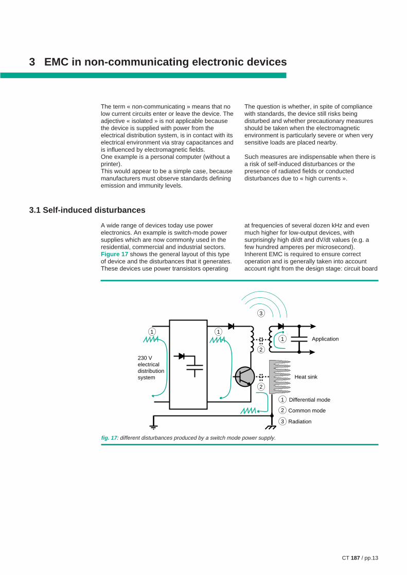
3 EMC in non-communicating electronic devices
The term « non-communicating » means that nolow current circuits enter or leave the device. Theadjective « isolated » is not applicable becausethe device is supplied with power from theelectrical distribution system, is in contact with itselectrical environment via stray capacitances andis influenced by electromagnetic fields.One example is a personal computer (without aprinter).This would appear to be a simple case, becausemanufacturers must observe standards definingemission and immunity levels.
The question is whether, in spite of compliancewith standards, the device still risks beingdisturbed and whether precautionary measuresshould be taken when the electromagneticenvironment is particularly severe or when verysensitive loads are placed nearby.
Such measures are indispensable when there isa risk of self-induced disturbances or thepresence of radiated fields or conducteddisturbances due to « high currents ».
3.1 Self-induced disturbances
A wide range of devices today use powerelectronics. An example is switch-mode powersupplies which are now commonly used in theresidential, commercial and industrial sectors.Figure 17 shows the general layout of this typeof device and the disturbances that it generates.These devices use power transistors operating
fig. 17 : different disturbances produced by a switch mode power supply.
Differential mode
Common mode
Radiation
230 V electrical distribution system
Application
Heat sink
1
111
2
3
2
2
3
at frequencies of several dozen kHz and evenmuch higher for low-output devices, withsurprisingly high di/dt and dV/dt values (e.g. afew hundred amperes per microsecond).Inherent EMC is required to ensure correctoperation and is generally taken into accountaccount right from the design stage: circuit board

CT 187 / pp.14
fig. 18 : inductive couplings due to loop presence: the lefthand line shows two large loops to supply the twocircuits; the righthand line is preferable.
routing (see fig. 18 ), limitation of straycapacitances, shields, HF filters on the mainsside, minimum distances from disturbing cables,etc, with tests to ensure compliance.In spite of all the above, the risk of self-induced
disturbances remains, due in particular todevices frequently being implemented differentlyfrom standard test implementation: for exampleinsufficient earthing links which are too long andsuitable for common-impedance coupling, etc.
H
3.2 Exposure to radiated fields
Electric fieldsSurrounding electric fields can disturb a deviceand its supply circuits (50/60 Hz) via the antennaeffect.
Counter-measures include:c minimising the antenna effect (for example, noconductors with free ends, conductors near EBSconductive parts),c using HF filters on the power supply cable tostop incoming disturbances,c shielding the building by limiting the size ofopenings.
J
E
H
radiation
fig. 19 : slot coupling.
An opening of length l in a shield acts behaveslike a dipole of the same length (Babinet’sprinciple) and re-radiates part of the incidentfield from the other side of the shield. Openingtransparency becomes total when l ≥ λ/2.Beneath its resonance frequency, i.e. whenl < λ/2 (a condition encountered in lowfrequency phenomena) a slot can be likened toan inductance which equals roughly 1 nH/cm. Asurface current J broken by such a slotgenerates a difference in potential between itsedges and lets through some magnetic field. Itthen radiates an electric field E at right anglesand a magnetic field H (dominant) parallel to itslength.
Magnetic fields
The attenuation resulting from shields dependsmainly on absorption which is reverselyproportional to skin depth (δ). For steel thisis 0.07 mm at 30 kHz and 1.7 mm at 50 Hz,whereas for copper it is 10 mm at 50 Hz!(attentuation is 8.7 dB where shieldingthickness e = δ).
The above makes clear that effective shields inlow frequency is very difficult and costly. What ismore, some openings or slots allow penetration ofinduction by magnetic dipole effect (see fig. 19 ).

CT 187 / pp.15
The magnetic field penetrating the system and/orthe magnetic fields generated in the cubicle byhigh currents, induce common mode anddifferential mode voltages in the loops.
Note that attenuation of LF magneticdisturbances arriving via the power supply cable,using standard filters (termed « HF »), is verylimited.
In buildings, radiated magnetic fields may have anumber of sources, notably lightning, transformerleakage flux, incoming and outgoing circuits ofstatic converters as well as the protectiveconductors of TN-C systems. This case isillustrated in figure 20 .
Take the case of a power cable running in abuilding void. The system is TN-C. The loadimbalance current flows continuously through theprotective conductor (PE), which is also theneutral conductor (N), along with the third orderharmonic currents and their multiples. Use ofnon-linear loads such as static converters and inparticular switch mode power supplies isresponsible for the increasing importance ofthese harmonic currents.
Due to the current drawn off to the metallicstructure of the building, the vectorial sum of thecurrents in the cable is not equal to zero.
This differential current, which may amount toseveral dozen amperes, generates, over adistance d, a disturbing magnetic field H = Ι/2πd.
For example a 63 A current generates, over10 metres, a 1 A/m field which is sufficient todisturb not only cathode ray tubes but alsocertain magnetic components, giventhat HF shields do not block LF magnetic fields.Note that the magnetic field developed in the
fig. 20 : magnetic radiation due to neutral or faultcurrent in TN-C system.
VISU
ΣI ≠ 0
PEN PhasesMetal structures of building
H
H
event of an insulation fault, still in the TN system,is very strong (Id = Icc).
For low frequency magnetic fields, the counter-measures are:c distance,c power cables incorporating the phase, theneutral and the protective conductor. Single-corecables must be avoided wherever possible,c a suitable system earthing arrangement,c metal trunking (mitigating plane),c use of metal enclosures, preferably ferro-magnetic.
3.3 Conducted disturbances
Above 1 MHz, the impedance of cables rapidlylimits the level of disturbances (L = 1 µH/m).Troublesome disturbances are therefore madeup essentially of harmonics, overvoltages due toswitching and lightning voltages and currents.c Harmonic voltages are, generally speaking, nottroublesome for non-communicating devices.They may disturb controlled rectifiers (variationof zero crossing point).c Harmonic currents may generate, throughinductive crosstalk, conducted disturbances inlow current circuits.
c Overvoltages due to switching or lightning maycause malfunctions or even the destruction ofcomponents. The counter-measure is the use ofsurge limiters (lightning arresters) or waveabsorbers combining filters, lightning arrestersand a shielded transformer. The latter attenuateHF disturbances and, above all, block common-mode LF voltages.

CT 187 / pp.16
4 EMC in communicating electronic devices
Communicating systems are more sensitive todisturbances than non-communicating devicesbecause digital links involve very low voltagelevels and are more exposed to disturbancesgenerated by common impedance and radiation.Digital signals are particularly sensitive totransient phenomena.Their susceptibility is increased by the increasinglengths of connections and number of sources ofdisturbances.
For disturbances with frequencies less than1 MHz, the phenomena that must be taken intoaccount are, once again, primarily the 50 Hzmains disturbances and harmonics, overvoltagesdue to switching and the effects of lightning.Switching overvoltages are generally differentialmode and are best blocked where emitted usingsurge limiters (RC circuits-ZnO limiters, etc).This subject will not be dealt with in this CahierTechnique (see CT 179).
fig. 21 : TN-C system; the neutral current developsdifferences in potential which disturb the voltagereferences of the digital links; the fault current(several kA) develops a destructive ∆V.
Device 1∆V
PENL
IdIn
Device 2
LVMV
Digitallink
∆V≠0
Id
(≈ 20 kA)
Device 1
Device 2
Conductive parts of building
LVMV
Digital link
PENL
fig. 22 : TN-C system with mesh bonding: thepermanent ∆V (unbalance, harmonic multiples of 3)and temporary ∆V (fault) is attenuated, but there are« stray currents »: risk of fire and disturbing magneticfields, including at power cable level (see fig. 20 ).

CT 187 / pp.17
4.1 Example of a disturbance caused by common impedance
Consider two communicating devices that arepart of a « distributed intelligence » system andsupplied by the same electrical distributionsystem.What happens when an insulation fault occurs(see fig. 21 ):If there is no mesh bonding in the TN-C system,the insulation fault generates a short-circuitcurrent Id.The voltage drop ∆d in the electricalequipotential bonding conductor may exceed halfphase voltage (PE cross-section < phase cross-section). This voltage is also present betweenthe exposed conductive parts of the two devices,which disturbs communication and may evenseriously damage the transmitters/receivers ofthe digital link if appropriate protection is not
∆V≠0
PEN L
Id
(≈ 20 kA)
Device 1
Device 2
LVMV
Digital link
Conductive partsof building
∆V≈0
PEN L
Id
(≈ 20 A)
RU
RN
Device 1
Device 2
LVMV
Digital link
Conductive partsof building
fig. 23 : TN-S diagram, temporary ∆V; the fault currentin the protection cable temporarily destroysequipotential-bonding. As the PE is connected to thestructures, division of currents and magnetic fieldsoccurs as in figure 20 .
fig. 24 : TT system; the low current in the PE does notdisturb the equipotential-bonding of the potentialreferences of the communicating electronic devices(RPE is low compared with RU and RN and Id small; themagnetic fields and ∆V are 1000 times smaller thanin TN-C or TN-S.
provided. This is because in cases where the lowcurrent cable is coaxial, ∆V will be applied indifferential mode. The figures 22, 23 and 24show what happens if the conductive parts aremeshed in the various earthing systempossibilities (on the second fault in the IT systemthe risks are the same as those present inthe TN-S).Note that if the mesh bonding of all conductiveparts is very dense, the problem ofthe ∆V ceases to exist in the TN system, but theinsulation fault current is now greater than 3PhIcc (very small impedance of the neutral returncircuit).What conclusions must be drawn for existing andnew buildings where conductive part meshbonding is insufficient?

CT 187 / pp.18
fig. 25 : disturbance of a digital link by inductive loopand the solution.
c Avoid system earthing arrangements which, inthe event of an insulation fault, generate a short-circuit current (see fig. 24 ).c Divide the fault currents by making numerousconnections between the exposed conductiveparts and the metal structure of the building.The ∆V is reduced to a minimum… however, theradiation of the power cables, including
Reduced earth (ground) loop
EBS loop
a - Loop formed by the electrical distributionsystem and the digital link
b - The trunking, connected to the exposedconductive parts of both devices, minimises theinduced current effect with the digital link
c - Using parallel trunkings for the power supplyand digital link: reduced loops, mitigating planesand effects attenuated by mesh bonding
the PE conductor, must be controlled (see thesection on radiated fields in the precedingsection).c Use twisted shielded pairs where possiblebecause the current flowing in the shield haslimited effects in view of the small transferimpedance.
4.2 Example of a disturbance caused by radiation
For two computers interconnected by a network(see fig. 25a ), what happens when lightningstrikes?Consider a lightning strike 200 m from thebuilding with di/dt = 25 x 109 A/s(Î = 25 kA, tm = 1 µs).If the loop, formed by the 50 Hz distributionsystem and the digital links (see fig. 25a ) formsa surface area of 50 m2 for the impulse field, theresulting EMF is equal to:
e = dφdt
= µ0SdHdt
=µ0S2πd
didt
e = 4π 10−7 502π 200
25 109 = 1.25 kV
That is a dangerously high level for the digitaltransmitters/receivers. If the loop is closed, it isthe resulting current that causes the damage.
What counter-measures can be used?Minimisation of loop surface, power cables, lowcurrent cables: the problem is that if the loop isopen, a voltage which is dangerous for electronicdevices is developed and, if it is closed, theinduced current (transfer impedance) will disturbthe signal or even destroy the transmitter-receiver circuits. Figure 25a shows that the loopmay be a large one.
A parallel earthing conductor, trunking or metaltube (see fig. 25b ) can be used to minimiseloop surface.
A word of warning, however, as this creates anEBS loop. The conductive link between the twocommunicating devices must therefore be a lowimpedance one to prevent developing inducedvoltage between the exposed conductive parts ofthe communicating devices (avoid pig tails). Notethat if this link impedance is small, a large part ofthe fault current will flow through it should aninsulation fault arise.
The solution is once again to mesh the exposedconductive parts as densely as possible in orderto divide the currents and/or an earthing systemwith low fault current.
Earth loops and EBS loops reduced
Digitallink
Power supply PE
H

CT 187 / pp.19
fig. 26 : separation of conductors of different types inthe same trunking.
≥ 10 cm
AnalogDigital
AnalogDigital
Power PowerdV/dtdI/dt
Whatever the circumstances we recommend thatyou apply the solution shown in figure 25c inwhich the high/low current loop is removed as isalso the EBS loop. Three conductors areconnected in parallel: the two trunkings and theprotective conductor (PE). The trunkings shouldpreferably be separate, follow the same routeand run close to one another: for example ariser. On a floor of a building (high currents ofreduced strength) the power and signal cablescan run on the same trunking (see fig. 26 ).The distance between power and signal cables ona metal trunking depends on a number of factors:c the level of immunity of the communicatingdevices,c the capacity of the communication protocols tomanage disturbed messages,c the distance over which the cables run together,c the current flowing in the power cables,c whether the cable contains the PE or single-pole conductors,
c the electrical characteristics of the signals(electrical level, frequency, impedance…).
Communicating equipment manufacturersrecommend a minimum distance,normally 30 cm. However the distance to beused in a given case should always be validatedby an expert.

CT 187 / pp.20
5 Conclusion
This Cahier Technique has shown that a variety ofprofessions are concerned by the cohabitation ofhigh and low currents. We have not dealt withcommunication softwares for which designers mustfind solutions for the disturances which couldaffect them. Electronic, electrical, automaticcontrol and software experts must join forces andwork together to design and produce installations.In France Sub-Committee 15D of the UTE iscurrently working on the guide designed to meetthis need.
Electronic engineers know that preference shouldbe given to shielded twisted cables, that thereshould be no conductors with free ends, thatcables should be flattened against an equipotentialmetal surface, that pig tails should be avoided andthat great care must be taken with choosing andimplementing cable glands. However they are notalways aware that it is highly advisable for lowcurrent cables to follow the paths of high currentones, that copper links between two buildings aredangerous even if their respective earthelectrodes are connected by a 35 mm2 conductor(L = 1 µH/m) and that exposed conductive partmesh bonding, if required, may cause problems(for example risk of fire in TN-C).
Electrical engineers are disturbed by thedistinction made between protective EBS
and EBS. They do not always understand theimportance of total mesh bonding and do notalways grasp why interconnection of exposedconductive parts and continuity of trunkings needto be ensured with such care.
We have shown that non-communicating devices,even when correctly designed and in compliancewith emission and immunity standards, arenonetheless affected by the disturbances andcoupling mechanisms found in installations andnot always perfectly elucidated.
Communicating systems, increasingly numerousand wide-spread, clearly pose the problem of howto make use of high currents and low currents in aspecific building. Inductive loops must be avoidedor shunted by a parallel earthing equipotentialbonding conductor. The best possibleequipotential bonding must be achieved for bothhigh and low frequencies, not only on each floor,but also between floors to form a completeequipotential bonding mesh. In all cases correctuse of cableways, trunkings and metal skirtingboards is vital.
Figure 27 reflects the electrical engineer’svision, that of the EMC expert, and offers aminimum, inexpensive solution for existingbuildings.

CT 187 / pp.21
PipesPEMetal
structures
1
2
2
2
3
3
3
a - Equipotential protection system with a bus (betweenfloors) and star (on each floor) topology. The same appliesto electrical power distribution.
c Purpose: safety of persons/indirect contactc Attributes:- no EBS loops,- possible calculation of fault current,- monitored fault current routing,- low impedance at 50 Hz but high in HF,- no common impedance coupling (except in TN at the riser).
parallel earthing conductors
high current trunkings
fig. 27 : searching for equipotential bonding in LF and HF.
c - Minimum protection and equipotential-bonding system.Optimum use of trunkings.
c Purpose: same as in figures 22a and 22b .c Attributes:- does away with high current/low current loops, earth loops andEBS loops,- HF equipotential-bonding,- LF equipotential-bonding (if low Id),- no stray currents,- mitigating plane effect/EM fields.NB:- can be completed by local meshed ground planes,- does not prevent direct links between two loads close to eachother (with parallel earthing conductor),- at floor level, a single trunking may be enough,- the riser in the centre limits external influences.
c On the upper floors, type 3 links must be provided if theelectrical equipment is less than one metre away from the metalstructures outside the building.
b - Meshed equipotential bonding system
c Purpose:- equipotential-bonding in HF,- low impedance in LF and HF.c Attributes:- random, multiple routing of 50 Hz fault currents and neutralcurrents (TN-C) as earths in PE,- small earth loops (HF),- common impedance coupling,- increased fault current in TN.NB: to ensure efficiency, particularly in HF, mesh bonding mustbe very dense.
Type 3 links, if made, create EBS loops which will affect deviceslocated on different floors.Thus, if links of this type are made, the equipotential bondingsbetween floors must be multiplied in order to minimise thesurface of the EBS loops.
(1) Equipotential-bonding conductor encirclingthe floor of a building.(2) Shield or parallel earthing conductor, metaltrunking.(3) Additional equipotential bonding conductor.
Safety and EMC
EMC equipotential-bonding
Electrical safety

CT 187 / pp.22
Standards
c IEC 1000-4: sections 2 to 13: Electromagneticcompatibility (EMC), part 4: testing andmeasurement techniques. (see fig. 6 )
c European Directive CEM 89/336/CEE
c UTE C 90-490: recommendations for cablingintelligent buildings, October 1995
Schneider Cahiers Techniques
c Les perturbations électriques en BT,Cahier Technique n°141, April 1991 -R. CALVAS
c EMC: electromagnetic compatibility,Cahier Technique n°149, August 1996 -F. VAILLANT
c Perturbations des systèmes électroniques etschémas des liaisons à la terreCahier Technique n°177, September 1995 -R. CALVAS
Various publications
c La compatibilité électromagnétiqueEditions Schneider 07/96 MD1CEM1F
c Manuel didactique CEMEditions Schneider 01/96 ART 62920
c REE April 96(Revue de l’électricité et de l’électronique)
c REE November 95
Appendix: bibliography

Schneider Direction Scientifique et Technique,Service Communication TechniqueF-38050 Grenoble cedex 9Fax: (33) 04 76 57 98 60
Design: AXESS - Saint-Péray (07).Photos: Merlin Gerin et Telemecanique.Printing: CLERC Fontaine - 1500.- 100 FF- ©
199
7 S
chne
ider
08-9786415