Embed Size (px)
Citation preview

University of Arkansas, FayettevilleScholarWorks@UARK
Theses and Dissertations
8-2013
CAD Tool Design for NCL and MTNCLAsynchronous CircuitsVijay Mani PillaiUniversity of Arkansas, Fayetteville
Follow this and additional works at: http://scholarworks.uark.edu/etd
Part of the Digital Circuits Commons, and the VLSI and Circuits, Embedded and HardwareSystems Commons
This Thesis is brought to you for free and open access by ScholarWorks@UARK. It has been accepted for inclusion in Theses and Dissertations by anauthorized administrator of ScholarWorks@UARK. For more information, please contact [email protected], [email protected].
Recommended CitationPillai, Vijay Mani, "CAD Tool Design for NCL and MTNCL Asynchronous Circuits" (2013). Theses and Dissertations. 829.http://scholarworks.uark.edu/etd/829


CAD TOOL DESIGN FOR NCL AND MTNCL ASYNCHRONOUS CIRCUITS

CAD TOOL DESIGN FOR NCL AND MTNCL ASYNCHRONOUS CIRCUITS
A thesis submitted in partial fulfillment of the requirements
for the degree of
Master of Science in Electrical Engineering
By
Vijay Pillai
University of Pune
Bachelor of Engineering in Electronics & Telecommunications, 2004
University of Arkansas
Master of Business Administration, 2010
August 2013
University of Arkansas
This thesis is approved for recommendation to the Graduate Council.
Thesis Director:
____________________________________
Dr. Scott Christopher Smith
Thesis Committee:
____________________________________ _____________________________________
Dr. Randy Brown Dr. Alan Mantooth
____________________________________
Dr. Jia Di

ABSTRACT
This thesis presents an implementation of a method developed to readily convert Boolean
designs into an ultra-low power asynchronous design methodology called MTNCL, which
combines multi-threshold CMOS (MTCMOS) with NULL Convention Logic (NCL) systems.
MTNCL provides the leakage power advantages of an all high-Vt implementation with a
reasonable speed penalty compared to the all low-Vt implementation, and has negligible area
overhead. The proposed tool utilizes industry-standard CAD tools. This research also presents
an Automated Gate-Level Pipelining with Bit-Wise Completion (AGLPBW) method to
maximize throughput of delay-insensitive full-word pipelined NCL circuits. These methods have
been integrated into the Mentor Graphics and Synopsis CAD tools, using a C-program, which
performs the majority of the computations, such that the method can be easily ported to other
CAD tool suites. Both methods have been successfully tested on circuits, including a
4-bit × 4-bit multiplier, an unsigned Booth2 multiplier, and a 4-bit/8-operation arithmetic logic
unit (ALU)

ACKNOWLEDGEMENTS
I owe sincere thankfulness to my research advisor, Dr. Scott Smith, who guided me
through the Master’s program. I am sure that this thesis would not have been possible without his
support, understanding and encouragement. Working with him has been a wonderful experience
and he has been extremely supportive of my endeavors outside the engineering curriculum.
I would like to show my gratitude to my brothers, sister-in-law, colleagues, and friends
for their help and moral support. I would also like to thank Hrishikesh Pai, for all his support and
inspiration.

DEDICATION
This thesis is lovingly dedicated to my parents, Laxmi Mani Pillai and S.V. Mani Pillai.
Their selfless love, support, guidance, and encouragement have sustained me throughout my life.

TABLE OF CONTENTS
1. Introduction 1
1.1 Objectives 1
1.2 Need for Asynchronous circuits 1
1.3 Thesis Overview 2
2. Introduction to NCL 3
2.1 Delay-insensitivity 3
2.2 NCL logic gates 4
2.3 Input-completeness and observability 10
2.4 Dual-rail combinational NCL circuits design 12
2.5 NCL completion 13
3. Introduction to MTCMOS 14
4. Introduction to MTNCL 17
4.1 Early-Completion Input-Incomplete (ECII) MTNCL Architecture 17
4.2 MTNCL Threshold Gate Design for ECII Architecture 18
4.3 Delay-Insensitivity Analysis 20
5. MTNCL CAD tool 24
5.1 Process Input Boolean Circuit Design 26
5.2 Place all the corresponding MTNCL Gates in the Design 28
5.3 Insertion of Registration, Completion and Sleep Logic 30
5.4 Optimization of Design by Minimization 34
5.5 Place Component Definitions and Libraries 35
5.6 Creating the Equivalent MTNCL VHDL Design 36

5.7 MCT Implementation 37
6. Automated Gate-Level Pipelining with Bit-Wise Completion 38
6.1 Previous Work 38
6.2 Bit-Wise Completion Strategy 39
6.3 Automated Gate-Level Pipelining with Bit-Wise Completion tool 40
7. Simulation Results 44
7.1 MTNCL CAD tool 44
7.2 Automated Gate-Level Pipelining with Bit-Wise Completion Tool 46
8. Conclusion and Future Work 49
8.1 MTNCL CAD tool 49
8.2 Automated Gate-Level Pipelining with Bit-Wise Completion Tool 50
References 51

1
Chapter 1. Introduction
1.1 Objectives
This thesis has 2 main sections. First, an automated method is developed to convert gate-
level Boolean designs into an equivalent gate-level MTNCL circuit. MTNCL is an ultra-low
power design methodology for asynchronous circuits, which combines Multi-Threshold CMOS
(MTCMOS) with NULL Convention Logic (NCL). Second, the thesis presents an Automated
Gate-Level Pipelining method with Bit-Wise Completion (AGLPBW) to maximize throughput
of delay insensitive NCL circuits. Analytical and simulation results are discussed to validate the
proposed schemes.
1.2 Need for asynchronous circuits
Synchronous circuits are predominant in the semiconductor IC industry, in large part due
to the synthesis CAD tools which create optimized synchronous circuits from high-level
descriptions, with a shortened design cycle. However, as feature size diminishes, transistor count
escalates into the billions, and clock frequency increases. This causes the clock distribution,
process variation, and power dissipation to become severely problematic for synchronous
circuits. On the other hand, delay-insensitive (DI) asynchronous circuits, such as NCL, utilize
hand-shaking protocols with completion detection, thus removing clocks and the necessity for
complex timing analysis. The result is more robust with lower power consumption, making these
circuits an excellent choice in the long run. To support this, the International Technology
Roadmap for Semiconductors (ITRS) predicts that asynchronous circuits will account for 49% of
the multi-billion dollar industry by 2024 [1].

2
1.3 Thesis Overview
This thesis is organized into 8 chapters. Chapter 2 introduces NULL Convention Logic
(NCL). Chapter 3 introduces Multi-Threshold CMOS. Chapter 4 introduces MTNCL. These
chapters provide the basis for the rest of the research. Chapter 5 discusses the
implementation of a MTNCL CAD tool to convert synthesized Boolean designs
into their MTNCL version. Chapter 6 presents an Automated Gate-Level Pipelining with
Bit-Wise Completion (AGLPBW) method to maximize throughput of delay-insensitive NCL
circuits. Chapter 7 presents simulation results; and Chapter 8 concludes the research.

3
Chapter 2. Introduction to NCL
2.1 Delay-insensitivity
Generally, asynchronous circuits fall into one of two categories: bounded-delay model or
delay-insensitive model. NCL circuits belong to the delay-insensitive model, which means they
can operate correctly with little timing analysis [2]. Symbolic completeness of expression is
utilized in NCL to realize delay-insensitive behavior. Specifically, dual-rail and quad-rail logic
are used in NCL design. Symbolically complete means that the outputs are only determined by
the presence of the input signals, regardless of the timing relationship between the input signals
[4].
In NCL, both dual-rail and quad-rail signals use space optimal 1-hot encoding, requiring
two wires per bit. A dual-rail signal, D, comprises two wires: D0 and D
1. The value of D
0 and D
1
is chosen from the set {DATA0, DATA1, NULL}. DATA0 corresponds to logic 0 in Boolean
logic, with D0 =1 and D
1=0, while DATA1 is the same as logic 1 in Boolean logic, with D
0 =0
and D1=1. NULL means the dual-rail signal is not available, so D
0 =0 and D
1=0. Just as logic 0
and logic 1 are mutually exclusive in Boolean logic, DATA0 and DATA1 are also mutually
exclusive. Therefore, D0 and D
1 cannot be 1 simultaneously; this is an illegal state. Likewise, a
quad-rail signal uses
4 wires, D0, D
1,D
2, D
3, which can have a value of { DATA0, DATA1, DATA2, DATA3,
NULL}. A quad-rail signal corresponds to two Boolean logic signals, X and Y. DATA0 is
represented with D0 =1 and D
1 =0, D
2 =0, D
3 =0, which corresponds to X=0 and Y=0. DATA1 is
represented with D1 =1 and the rest of the rails are 0, which corresponds to X=0 and Y=1.
DATA2 is expressed as D2 =1 and the rest of the rails are 0, which corresponds to X=1 and Y=0.
DATA3 is expressed as D3 =1 and the rest of the rails

4
are 0, which corresponds to X=1 and Y=1. NULL means the data is not available, so all the rails
are 0. The four wires of a quad-rail signal are mutually exclusive, which means only one of them
can be asserted at a time. If more than one rail is asserted, this state is defined as an illegal state
[2], [5].
Figure 1. Example of Boolean OR gate and NCL OR function
We can see from Figure1 above that regular Boolean OR gate has an incorrect output
during the transition, while NCL OR function does not; the output is valid when DATA (non-
NULL).
2.2 NCL logic gates
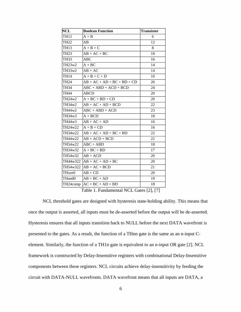
NCL logic is comprised of 27 fundamental gates. Each rail in NCL logic, both dual-rail
and quad-rail, counts as a separate variable. Each of the fundamental gates can have four or
fewer variables as its inputs. NCL gates are an extension of the C-element. A C-element output
assumes the value of the inputs when all inputs have the same value. Otherwise, the output stays
X
YZ
X
Y
Z
0
0
0
1
1
11 ns
incorrectvalid valid
NCL OR
Function
X0
X1
Y0
Y1
Z0
Z1
X0
X1
Y0
Y1
Z0
Z1
0
1
0
1
0
1
0
1
0
1
DATA0 NULL DATA1
0
1

5
at its previous value [2]. The primary type of NCL gate is the THmn gate, where 1 m n, as
shown in Figure 2 [2].
Figure 2. THmn NCL Gate [2], [7]
The THmn gate has n inputs and threshold of m. The output of the gate will only be
asserted when at least m inputs are asserted. The inputs are connected to the round part of the
gate. The output is connected from the pointed end of the gate [2].
Another type of NCL gate is called a weighted threshold gate, denoted as
THmnWw1w2…wR. This type of gate has a threshold of m and weight integer values
w1, w2, …wR applied to input1, input2, … inputR, where m wR > 1. Here 1 R < n, where n is
the number of inputs [2], [8]. Take TH23W2 gate for example. It has 3 inputs labeled as A, B,
C, shown in Figure 3. The threshold for the gate is 2, and weight for input A, W(A), is 2. In order
for the output to be asserted, either inputs B and C must be asserted or input A must be asserted.
Therefore, the Boolean function of this gate is
Z = A + BC. Some NCL gates have a reset input that is used to initialize the output. An
n inside an NCL gate means it is reset to 0, while a d means it is set to 1.
Figure 3. TH23W2 gate [2]
2
A
B
C
Z
m
Input 1Input 2
Input n
….. Output
6
NCL
Macro
Boolean Function Transistor
Count TH12 A + B 6
TH22 AB 12
TH13 A + B + C 8
TH23 AB + AC + BC 18
TH33 ABC 16
TH23w2 A + BC 14
TH33w2 AB + AC 14
TH14 A + B + C + D 10
TH24 AB + AC + AD + BC + BD + CD 26
TH34 ABC + ABD + ACD + BCD 24
TH44 ABCD 20
TH24w2 A + BC + BD + CD 20
TH34w2 AB + AC + AD + BCD 22
TH44w2 ABC + ABD + ACD 23
TH34w3 A + BCD 18
TH44w3 AB + AC + AD 16
TH24w22 A + B + CD 16
TH34w22 AB + AC + AD + BC + BD 22
TH44w22 AB + ACD + BCD 22
TH54w22 ABC + ABD 18
TH34w32 A + BC + BD 17
TH54w32 AB + ACD 20
TH44w322 AB + AC + AD + BC 20
TH54w322 AB + AC + BCD 21
THxor0 AB + CD 20
THand0 AB + BC + AD 19
TH24comp AC + BC + AD + BD 18
Table 1. Fundamental NCL Gates [2], [7]
NCL threshold gates are designed with hysteresis state-holding ability. This means that
once the output is asserted, all inputs must be de-asserted before the output will be de-asserted.
Hysteresis ensures that all inputs transition back to NULL before the next DATA wavefront is
presented to the gates. As a result, the function of a THnn gate is the same as an n-input C-
element. Similarly, the function of a TH1n gate is equivalent to an n-input OR gate [2]. NCL
framework is constructed by Delay-Insensitive registers with combinational Delay-Insensitive
components between these registers. NCL circuits achieve delay-insensitivity by feeding the
circuit with DATA-NULL wavefronts. DATA wavefront means that all inputs are DATA, a

7
combination of DATA0 and DATA1; while NULL wavefront means all inputs are NULL.
DATA wavefronts are separated by NULL wavefronts to make sure that current DATA
wavefronts don’t overwrite previous DATA wavefronts, thus eliminating the race condition.
When all inputs of a circuit become DATA, the output transitions to DATA. Then NULL
wavefront is fed into the circuit to make the output change to NULL. After that, another DATA
wavefront is fed into the circuit, to produce DATA at the output [2].
Figure 4. a) DATA Wavefront [2]
Figure 4. b) DATA Completion Detection [2]
NCL
Register 0
In Out
Ko Ki
NCL
Register 1
In Out
Ko Ki
NCL
Combinational
Circuit
Completion
Detection
DATA DATA
n n m m
NULL NULL
mn
0 1 1 0
NCL
Register 0
In Out
Ko Ki
NCL
Register 1
In Out
Ko Ki
NCL
Combinational
Circuit
Completion
Detection
DATA DATA
n n m m
DATA DATA
mn
0 1 0 1

8
Figure 4. c) NULL Wavefront [2]
Figure 4. d) NULL Completion Detection [2]
Handshaking signals, Ki and Ko, are used in DI registers to request and acknowledge
DATA and NULL wavefronts between adjacent stages [2].
Figure 5. NCL System Framework [2]
Similar to clock period in synchronous circuits, the DATA-to-DATA cycle, denoted as
TDD, is used to measure the speed of a NCL circuit. TDD is considered to be maximum delay of
any stage in a pipelined NCL circuit in the worst case scenario. To account for both the DATA
NCL
Register 0
In Out
Ko Ki
NCL
Register 1
In Out
Ko Ki
NCL
Combinational
Circuit
Completion
Detection
NULL NULL
n n m m
DATA DATA
mn
1 0 0 1
NCL
Register 0
In Out
Ko Ki
NCL
Register 1
In Out
Ko Ki
NCL
Combinational
Circuit
Completion
Detection
NULL NULL
n n m m
NULL NULL
mn
1 0 1 0
n
n
NCL Reg
In Out
Ko Ki
NCL
Combinational
Circuit
Completion
Detection
n n
n
In Out
Ko Ki
NCL
Combinational
Circuit
Completion
Detection
n n
n
…….
NCL Reg
n
n
In Out
Ko Ki
n
NCL Reg

9
and NULL wavefront, TDD is calculated as twice the sum of the worst case delay of
combinational and completion delay [2], [8].
Figure 6. DATA-NULL cycle [3]
A single bit dual-rail register is shown in Figure 7. This dual-rail register consists of
TH22 gates, with data inputs and Ki connected to inputs of TH22 gate. If Ki is request for data
(rfd, logic1), it will allow DATA value at the input to pass through. Similarly, it will pass NULL
at the input when Ki is request for null (rfn, logic0). The inverting TH12 gate (i.e., NOR gate) is
used to generate acknowledge signal, Ko. Ko will be rfn if the register output is DATA; it will be
rfd if the register output is NULL. The acknowledgement signals are combined in Completion
Detection circuitry, in Figure 8, to produce the request signals for the previous register stage.
Figure 7. Dual-Rail register [2]
2n
2n Outo1
1
Outo0
Ino1
Ino0
Ki
Ko
Reset
DATA Combinational
Evaluation
DATA Completion
Acknowledgement
NULL Combinational
EvaluationNULL Completion
Acknowledgement
DATA-to-DATA Cycle Time ( TDD )

10
Since the maximum number of inputs for a single gate is 4, we use TH44 gates in the
Completion Detection. As a result, the gate delay of the Completion Detection component,
combining N number of Ko signals from separate registers, is log4N [8].
Figure 8. N-bit Completion Detection Component [2], [8]
2.3 Input-completeness and observability
To achieve delay-insensitivity, NCL circuits must be input-complete and observable [2].
Input-complete means that the complete set of outputs of a combinational circuit cannot change
from NULL to DATA until all inputs are DATA; and the complete set of output cannot transition
from DATA to NULL until all inputs become NULL. As stated by Seitz’s “weak condition” of
delay-insensitive signaling [6], for a circuit which has more than one output, some of the outputs
4
4
4
4
4
4
4
4
4
4
….
…. 4
….
….
…. Ko
Ko(N)
Ko(N-1)
Ko(N-2)
Ko(N-3)
Ko(N-4)
Ko(N-5)Ko(N-6)
Ko(N-7)
Ko(N-8)
Ko(N-9)
Ko(N-10)
Ko(N-11)
Ko(N-12)
Ko(N-13)
Ko(N-14)
Ko(N-15)
Ko(4)Ko(3)
Ko(2)Ko(1)
Ko(8)Ko(7)
Ko(6)Ko(5)
Ko(12)Ko(11)
Ko(10)
Ko(9)
Ko(16)Ko(15)
Ko(14)
Ko(13)

11
can transition before a complete set of inputs are present, on the condition that all outputs cannot
transition before all inputs arrive. Consider a NCL half adder in Figure 9.
Figure 9. NCL Half Adder [2]
The output sum is input-complete with respect to X and Y, but Cout is not input-complete.
However, the whole set of {sum, Cout } is input-complete, because when S transitions to DATA,
both inputs must be DATA. On the other hand, the hysteresis property of NCL gates requires that
all inputs must transition to NULL before the output can transition to NULL, thus guaranteeing
the output is input-complete with respect to NULL. When deriving equations for a NCL circuit,
by making sure every non-don’t care product term contains any rail of a particular input, we can
make the NCL circuit input-complete with respect to that input.
In order to achieve observability, there must be no orphans propagating through a gate
[2]. The definition of an orphan is a wire not used to determine the output, that transitions during
the current DATA wavefront. Observability ensures that any transition of an internal gate causes
at least one of the circuit outputs to transition. That means if the output of one gate is connected
AB
C
D
F
TH24comp
AB
C
D
F
TH24comp
1
X0
Y0
2
X1
Y1
Co0
Co1
S0
S1

12
to inputs of other gates, it is imperative that the transition on this gate causes at least one output
of the other gates to transition [5].
2.4 Dual-rail combinational NCL circuit design
Designing dual-rail combinational NCL circuits using a K-map is very similar to the
procedure used to design regular synchronous combinational circuits. The difference is that
equations are needed for both rail1 and rail0. After equations are obtained, we need to see if they
are input-complete. If not, the missing input terms need to be added to the product terms in the
equations. In addition, it is necessary to carefully map the equations using the 27 NCL gates to
ensure observability by not partitioning product terms [2].
For example, consider the design of an NCL AND function with 2-inputs
0 1
0 0 0
1 0 1
Minimized equation for AND2 can be found as :
F1= A
1 B
1 (2.1)
F0= A
0 +B
0 (2.2)
Notably, rail1 is input-complete to A and B. However, rail0 is not input-complete. So, the
missing input needs to be added to each of the terms.
F1
= A0 +B
0 (2.3)
= A
0(B
0 +B
1) + B
0 (A
0 +A
1)
B
A

13
= A0 B
0 + A
0 B
1 + A
1 B
0
By multiplying redundant terms, rail0 is input-complete to both A and B.
2.5 NCL completion
NCL can be divided into two completion categories. The first is full-word completion and
the second is bit-wise completion. Full-word completion requires that the completion signals
from each bit of the receiving stage be conjoined together by completion component and sent
back to the sourcing stage. Bit-wise completion only returns completion signals from a specific
bit back to the bits in a previous stage that are used to calculate this bit [2], [8].

14
Chapter 3. Introduction to MTCMOS
MTCMOS reduces leakage power by disconnecting the power supply from the circuit
during idle (or sleep) mode while maintaining high performance in active mode by utilizing
different transistor threshold voltages (Vt) [12]. Low-Vt transistors are faster but have high
leakage, whereas high-Vt transistors are slower but have far less leakage current. MTCMOS
combines these two types of transistors by utilizing low-Vt transistors for circuit switching to
preserve performance and high-Vt transistors to gate the circuit power supply to significantly
decrease sub-threshold leakage.
One MTCMOS method uses low-Vt transistors for critical paths to maintain high
performance, while using slower high-Vt transistors for the non-critical paths to reduce leakage.
Besides this path replacement methodology, there are two other architectures for implementing
MTCMOS. A course-grained technique investigated in [13] uses low-Vt logic for all circuit
functions and gates the power to entire logic blocks with high-Vt sleep transistors, denoted by a
dotted circle, as shown in Figure 10. The sleep transistors are controlled by a Sleep signal.
During active mode, the Sleep signal is de-asserted, causing both high-Vt transistors to turn on
and provide a virtual power and ground to the low-Vt logic. When the circuit is idle, the Sleep
signal is asserted, forcing both high-Vt transistors to turn off and disconnect power from the low-
Vt logic, resulting in a very low sub-threshold leakage current. One major drawback of this
method is that partitioning the circuit into appropriate logic blocks and sleep transistor sizing is
difficult for large circuits. An alternative fine-grained architecture, shown in Figure 11,
incorporates the MTCMOS technique within every gate [14], using low-Vt transistors for the
Pull-Up Network (PUN) and Pull-Down Network (PDN) and a high-Vt transistor to gate the
leakage current between the two networks. Two additional low-Vt transistors are included in

15
parallel with the PUN and PDN to maintain nearly equivalent voltage potential across these
networks during sleep mode (i.e., X1 is approximately VDD and X2 is approximately GND).
Implementing MTCMOS within each gate resolves the issue of logic block partitioning and sleep
transistor sizing, since each gate within the gate library is sized separately. However, this results
in a large area overhead.
In general, three serious drawbacks hinder the widespread usage of MTCMOS in
synchronous circuits [13]: 1) the generation of Sleep signals is timing critical, often requiring
complex logic circuits; 2) synchronous storage elements lose data when the power transistors are
turned off during sleep mode; and 3) logic block partitioning and transistor sizing is very
difficult for the course-grained approach; and the fine-grain approach results in excessive area
overhead. However, all three of these drawbacks are eliminated by utilizing NCL in conjunction
with the MTCMOS technique.

16
VDD
Low-Vt CMOS Logic
SLEEP
SLEEP
INPUTS OUTPUTS
Virtual VDD
Virtual GND
Reduce sub-threshold
leakage during sleep mode
Reduce sub-threshold
leakage during sleep mode
Maintain high performance
during active mode
Figure 10. General MTCMOS circuit architecture [13].
Figure 11. MTCMOS applied to a Boolean gate [14].
PUN
PDN
Sleep
Sleep
Sleep
In 1
In n
Out
P 0
P 1
N 0
X 1
X 2

17
Chapter 4. Introduction to MTNCL
MTNCL was originally developed in [14-18], as summarized below.
4.1 Early-Completion Input-Incomplete (ECII) MTNCL Architecture
NCL threshold gates are larger and implement more complicated functions than basic
Boolean gates, such that fewer threshold gates are needed to implement an arbitrary function
compared to the number of Boolean gates. However, the NCL implementation often requires
more transistors. Consequently, incorporating MTCMOS inside each threshold gate facilitates
easy sleep transistor sizing without requiring as large of an area overhead. Since floating nodes
may result in substantial short circuit power consumption at the following stage, an MTCMOS
structure similar to the one shown in Figure 11 is used to pull the output node to ground during
sleep mode. When all MTNCL gates in a pipeline stage are in sleep mode, all gate outputs are
logic 0. At this point the pipeline stage is in the NULL state. Hence, after each DATA cycle, all
MTNCL gates in a pipeline stage can be forced to output logic 0 by asserting the sleep control
signal instead of propagating a NULL wavefront through the stage; hence, data is not lost during
sleep mode.
Since the completion detection signal, Ko, indicates whether the corresponding pipeline
stage is ready to undergo a DATA or NULL cycle, Ko can be naturally used as the sleep control
signal without requiring any additional hardware. This is in contrast to the complex Sleep signal
generation circuitry needed for synchronous MTCMOS circuits. Unfortunately, the direct
implementation of this idea using regular NCL completion compromises delay-insensitivity [18].
To solve this problem, Early Completion [20] can be used in lieu of regular completion, as
shown in Figure 12, where each completion signal is used as the sleep signal for all threshold
gates in the subsequent pipeline stage. Early Completion utilizes the inputs of registeri-1 along

18
with the Ki request to registeri-1, instead of just the outputs of registeri-1 as in regular completion,
to generate the request signal to registeri-2, Koi-1. The combinational logic will not be put in sleep
mode until all inputs are NULL and the stage is requesting NULL. Therefore the NULL
wavefront is ready to propagate through the stage, so the stage can instead be put to sleep
without compromising delay-insensitivity. The stage will then remain in sleep mode until all
inputs are DATA and the stage begins requesting DATA, and is therefore ready to evaluate. This
Early Completion MTNCL architecture, denoted as ECII, ensures input-completeness and
observability through the sleep mechanism (i.e., the circuit is only put to sleep after all inputs are
NULL, when all gates are then simultaneously forced to
logic 0, and only evaluates after all inputs are DATA), such that input-incomplete logic functions
can be used to design the circuit, decreasing area and power and increasing speed.
DI
Register
i-2
Ki
MTNCL
Logic
DI
Register
i-1
Ki
Early
Completion
MTNCL
Logic
DI
Register
i
Ki
Early
Completion
SleepSleep
Early
Completion
Sleep
Koi-1
Figure 12. MTNCL pipeline architecture using Early Completion.
4.2 MTNCL Threshold Gate Design for ECII Architecture
The MTCMOS structure is incorporated inside each NCL threshold gate, causing a
number of the original transistors to become irrelevant. As shown in Figure 13a, the reset
circuitry is no longer necessary, as the gate output will now be forced to NULL by the
MTCMOS sleep mechanism. Hold1 is used to ensure that the gate remains asserted until all
inputs are de-asserted, in order to guarantee input-completeness with respect to the NULL

19
wavefront. However, since the ECII architecture guarantees input-completeness through the
sleep mechanism, as explained in Chapter 4.1, it follows that NCL gate hysteresis is no longer
required. Hence, the hold1 circuitry and corresponding NMOS transistor are removed, and the
PMOS transistor is removed to maintain the complementary nature of CMOS logic (i.e., set and
hold0 are complements of each other), such that the gate is never floating.
Improved from the direct MTCMOS NCL threshold gate implementation [15] similar to
the structure shown in Figure 11, a modified Static MTNCL threshold gate structure, referred to
as SMTNCL, is shown in Figure 13b. This modification eliminates the output wake-up glitch by
moving the power gating high-Vt transistor to the PDN, and removing the two bypass transistors.
All PMOS transistors except the output inverter are high-Vt, because they are only turned on
when the gate enters sleep mode and the inputs become logic 0, and remain on when the gate
exits sleep mode, until the gate’s set condition becomes true. In both cases, the gate output is
already logic 0. Therefore, the speed of these PMOS transistors does not affect performance, so
high-Vt transistors are used to reduce leakage current. During active mode, the Sleep signal is
logic 0 and Sleep is logic 1, such that the gate functions as normal. During sleep mode, Sleep is
logic 1 and Sleep is logic 0, such that the output low-Vt pull-down transistor is turned on quickly
to pull the output to logic 0, while the high-Vt NMOS gating transistor is turned off to reduce
leakage. Note that since the internal node, between set and hold0, is logic 1 during sleep mode
and the output is logic 0, the NMOS transistor in the output inverter is no longer on the critical
path and therefore can be a high-Vt transistor. As an example, this SMTNCL implementation of
the static TH23 gate is shown in Figure 13c.

20
Reset hold0
Z
set hold1
a)
hold0
(high-Vt)
set
OutputSleep
Sleep
C
B
A
A
B C C
Z
B
Sleep
C
A
Sleep
b) c)
Figure 13. (a) Incorporating MTCMOS into NCL threshold gates, (b) SMTNCL gate structure,
and (c) TH23 implementation.
4.3 Delay-Insensitivity Analysis
Combining the ECII architecture with the SMTNCL gate structure, results in a delay-
sensitivity problem, as shown in Figure 14. After a DATA cycle, if most, but not all, inputs
become NULL, this Partial NULL (PN) wavefront can pass through the stage’s input register,
because the subsequent stage is requesting NULL, and cause all stage outputs to become NULL,

21
before all inputs are NULL and the stage is put to sleep, because the hold1 logic has been
removed from the SMTNCL gates. This violates the input-completeness criteria, discussed in
Chapter 2, and can cause the subsequent stage to request the next DATA while the previous
stage input is still a partial NULL, such that the preceding wavefront bits that are still DATA will
be retained and utilized in the subsequent operation, thereby compromising delay-insensitivity,
similar to the problem when using regular completion instead of Early Completion for MTNCL
[18].
There are two solutions to this problem, one at the architecture level and the other at the
gate level. Since the problem is caused by a partial NULL passing through the register, this can
be fixed at the architecture-level by ensuring that the NULL wavefront is only allowed to pass
through the register after all register inputs are NULL, which is easily achievable by using the
stage’s inverted sleep signal as its input register’s Ki signal. This Fixed Early Completion Input-
Incomplete (FECII) architecture is shown in Figure 15. Compared to ECII, FECII is slower
because the registers must wait until all inputs become DATA/NULL before they are latched.
Note that a partial DATA wavefront passing through the register does not pose a problem,
because the stage will remain in sleep mode until all inputs are DATA, thereby ensuring that all
stage outputs will remain NULL until all inputs are DATA.
This problem can also be solved at the gate level by using the new SMTNCL1 gate
shown in Figure 16, to ensure input-completeness with respect to NULL, such that a partial
NULL wavefront cannot cause all outputs to become NULL. Note that the feedback NMOS
transistor holds the output at logic1, which ensures that once the output of the gate has been
asserted due to current DATA wavefront, it will only get de-asserted when the sleep signal is

22
activated for the gate (i.e., when all circuit inputs are NULL), and will block a partial NULL
wavefront from de-asserting the gate output.
To summarize, the ECII architecture only works with new SMTNCL1 gates. However,
FECII works better with the SMTNCL gates since they require fewer transistors. Additionally,
the ECII architecture is faster than FECII, when both use the same MTNCL gates.
rfd
rfn
rfnrfn
Previous Partial DATA
can propagate through C/L
DI
Register
Ki
MTNCL
Logic
DI
Register
Ki
Early
Completion
MTNCL
Logic
DI
Register
Ki
Early
Completion
SleepSleep
Early
Completion
Sleep
PN PN N N N D
Figure 14. Delay-sensitivity problem combining ECII architecture with SMTNCL gates.
DI
Register
Ki
MTNCL
Logic
DI
Register
Ki
Early
Completion
MTNCL
Logic
DI
Register
Ki
Early
Completion
SleepSleep
Early
Completion
Sleep
Figure 15. Fixed Early Completion Input-Incomplete (FECII) architecture.

23
hold0
(high-Vt)
set
Output
Sleep
Sleep
A
B A B
C
C
B
A
C
A
Sleep
Sleep
Z
a) b)
Figure 16. (a) New SMTNCL1 gate structure, and (b) TH23 implementation.

24
Chapter 5. MTNCL CAD Tool
This thesis develops an automated tool to convert combinational Boolean circuits into
their equivalent MTNCL circuits. The process flow for this conversion is shown in Figure 17.
The conversion process starts with combinational Boolean design like a full adder circuit, which
is then synthesized into hierarchical gate level design using the industry standard Synopsys
synthesis tool. The MTNCL CAD Tool (MCT) accepts the hierarchical design as input, along
with the Synopsys log file and outputs the MTNCL equivalent circuit for the Boolean design.
Synopsys Synthesis tool
MTNCL CAD tool
Gate level boolean
design file Synthesis Log File
MTNCL design
Combinational boolean design
Figure 17. Process Flow for MTNCL conversion
The Synopsys CAD tool, Design Vision, is used for initial synthesis and could be run in
GUI or batch mode. The standard GTECH library is used as the target library for the purpose of

25
synthesis. The “SET_DONT_USE” command is used such that only the gates mentioned in Table
2 are employed.
Table 2. GTECH Library – Gates used for synthesis
A sample batch script for synthesis is shown in Figure 18.
Figure 18. Sample script for Synopsys Design Vision.
On successful completion of synthesis, we get a gate-level hierarchical circuit, which is
used as an input for the MTNCL CAD tool. Thereafter, the MTNCL CAD tool translates the
GTECH Library – Gates
GTECH_NOT
GTECH_AND2
GTECH_AND3
GTECH_AND4
GTECH_NAND2
GTECH_NAND3
GTECH_NAND4
GTECH_OR2
GTECH_OR3
GTECH_OR4
GTECH_NOR2
GTECH_NOR3
GTECH_NOR4
GTECH_XOR2
GTECH_XNOR2
GTECH_ADD_AB
GTECH_ADD_ABC
GTECH_MUX2
GTECH_MUX4
read_file /opt/ELEG_Software/Synopsys/synthesis/libraries/syn/gtech.db
read_file -format vhdl {full_add.vhd}
set_dont_use gtech/GTECH_LIST
compile -exact_map
write -hierarchy -format vhdl -output Boolean_design.vhd

26
design into its equivalent MTNCL circuit. The flowchart for the MTNCL CAD tool is shown in
Figure 19. This tool is comprised of several steps, described in the following subsections.
Process Input boolean circuit
Hierarchical gate-level boolean combinational
circuit
Place all corresponding MTNCL components in the
design
Insertion of Sleep Logic, Registration and Completion logic
Optimization of design
Equivalent MTNCL circuit
Place component definitions and libraries
Look-Up Table (LUT)
MTNCL Gate Definitions
Figure 19. MTNCL CAD tool flowchart
5.1 Process Input Boolean Circuit Design
MCT first reads the Synopsys log file named “command.log”. MCT searches for the main
design entity name in file. The last instance of the pattern: “read_file -format vhdl” has the

27
main design name specified at the end of the corresponding line. For example, in the log file
snippet shown below design name is full_add.
MCT assumes the file name to be the same as the entity name for standardization. This name
is stored in a variable named main_entity. MCT then reads the Boolean circuit’s VHDL
description, which is the output from the synthesis tool (i.e., Design Vision of the Synopsys
CAD tool suite) so as to be in a standardized format. The output VHDL file from the synthesis
tool is named “Boolean_design.vhd” for uniformity. MCT reads and stores the input and output
signals of the main entity in two separate arrays. Each array element is a data structure as defined
below.
Struct Signals
char name[]
char type[]
int size
Information related to input signals is stored in main_inputs[], and that pertaining to output
signals is stored in main_outputs[]. For demonstration, we will consider the example of a full
adder circuit that needs to be converted to its MTNCL equivalent. The full adder circuit, shown
in Figure 20, is the output from the synthesis tool, a VHDL hierarchical model.
read_file -format vhdl {/home/vpillai/DV/full_add.vhd}

28
A
B
Cin
Sum
Cout
GTECH_XOR2GTECH_XOR2
GTECH_NAND2 GTECH_NAND2
GTECH_NAND2
Figure 20. Full Adder Circuit (Output from Synthesis tool)
In the full adder example,
main_inputs[0].name=’A’; main_inputs[0].type=’std_logic’; main_inputs[0].size=1
main_inputs[1].name=’B’; main_inputs[1].type=’std_logic’; main_inputs[1].size=1
main_inputs[2].name=’Cin’; main_inputs[2].type=’std_logic’; main_inputs[2].size=1
main_outputs[0].name=’Sum’; main_outputs[0].type=’std_logic’;main_outputs[0].size=1
main_outputs[1].name=’Cout’; main_outputs[1].type=’std_logic’;main_outputs[1].size=1
This data structure is used for remapping of input and output ports while adding the register and
completion logic to the circuit design.
5.2 Place all the corresponding MTNCL Components in the Design
After extracting the circuit inputs and outputs from the main design’s VHDL description, the
next step is to parse through the input design file called “Boolean_design.vhd” and make gate
replacements as per the lookup table (LUT) shown in Table 3 below. The lookup table is
programmable and hence could be easily adapted for a different target library or for a different
technology. MCT programs the lookup table before every run. In its initialization routine, the
program reads a file named “program_LUT.txt” and updates its internal lookup data structure
accordingly. The LUT has two columns of data. The values in the first column of table array are

29
the values searched by a key (lookup value). These values can only be names of the GTECH
library gates.
When the MCT parser encounters any of the GTECH library gates in the input design file, it
uses the corresponding gate as the lookup value (key) to search the first column of the LUT and
returns the equivalent MTNCL component in the same row from the second column of the LUT.
MCT then uses the returned MTNCL component as a replacement for the GTECH library gate in
the input circuit.
BOOLEAN GATE (Key) MTNCL COMPONENT
GTECH_NOT INV
GTECH_AND2 AND2M
GTECH_AND3 AND3M
GTECH_AND4 AND4M
GTECH_NAND2 NAND2M
GTECH_NAND3 NAND3M
GTECH_NAND4 NAND4M
GTECH_OR2 OR2M
GTECH_OR3 OR3M
GTECH_OR4 OR4M
GTECH_NOR2 NOR2M
GTECH_NOR3 NOR3M
GTECH_NOR4 NOR4M
GTECH_XOR2 XOR2M
GTECH_XNOR2 NXOR2M
GTECH_MUX2 MUX21M
GTECH_MUX4 MUX41M
GTECH_ADD_AB HAM
GTECH_ADD_ABC FAM
Table 3. Programmable Lookup Table
After all the Boolean gates have been replaced, MCT then converts all the inputs, outputs, and
internal signal definitions from std_logic and std_logic_vector to dual_rail_logic and

30
dual_rail_logic_vector, respectively. Considering the full adder circuit as an example, Figure 21
shows the result of the LUT operation.
A
B
Cin
Sum
Cout
XOR2MXOR2M
NAND2M
NAND2M
NAND2M
Figure 21. Full Adder MTNCL Circuit
In Figure 21, inputs A, B, Cin, and outputs Sum, Cout are dual_rail_logic. The program also
maintains a separate array named gate_array for the MTNCL gates fetched from the LUT. For
example, if the values {gtech_not, gtech_and2, gtech_or2} were found in the input design file,
then gate_array should have corresponding replacement values {inv, and2m, or2m}. The
elements of this array are unique, i.e., no duplicates are allowed. Please refer to Section 5.5 of
this thesis to learn how this array is used in the placing of component definitions.
5.3 Insertion of Registration, Completion and Sleep Logic
For the purpose of this thesis, we chose to implement the Fixed Early Completion Input
Incomplete (FECII) architecture of MTNCL [2]. This architecture avoids delay-insensitivity
issues by ensuring that the NULL wavefront is only allowed to pass through the register after all
register inputs are NULL, which is achieved by using the stage’s inverted sleep signal as its input
register’s Ki signal as shown in Figure 22.
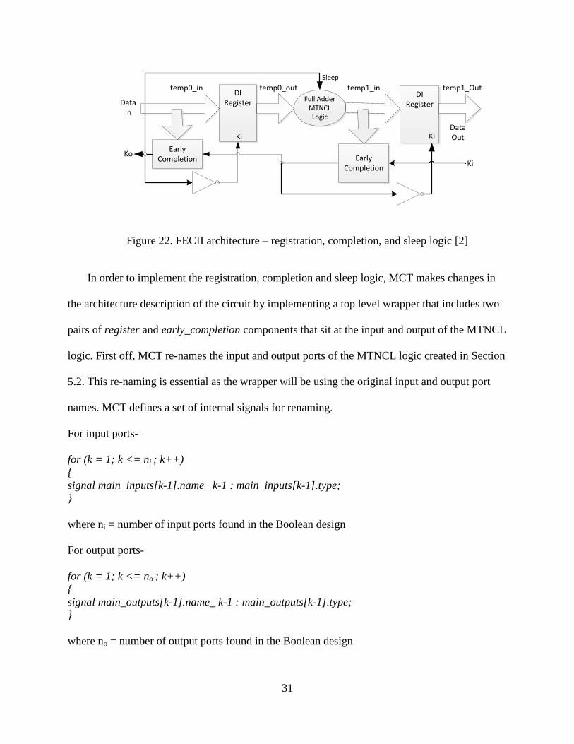
31
DI Register
Ki
Full Adder MTNCL Logic
DI Register
Ki
Early Completion
Sleep
Early Completion
KiKo
Data In
Data Out
temp0_in temp0_out temp1_in temp1_Out
Figure 22. FECII architecture – registration, completion, and sleep logic [2]
In order to implement the registration, completion and sleep logic, MCT makes changes in
the architecture description of the circuit by implementing a top level wrapper that includes two
pairs of register and early_completion components that sit at the input and output of the MTNCL
logic. First off, MCT re-names the input and output ports of the MTNCL logic created in Section
5.2. This re-naming is essential as the wrapper will be using the original input and output port
names. MCT defines a set of internal signals for renaming.
For input ports-
for (k = 1; k <= ni ; k++)
{
signal main_inputs[k-1].name_ k-1 : main_inputs[k-1].type;
}
where ni = number of input ports found in the Boolean design
For output ports-
for (k = 1; k <= no ; k++)
{
signal main_outputs[k-1].name_ k-1 : main_outputs[k-1].type;
}
where no = number of output ports found in the Boolean design
32
For the full adder example, the input ports would be renamed as A_0, B_1, and Cin_2; while
output ports would be renamed as Sum_0 and Cout_1. Thus, the full adder MTNCL circuit
depicted in Figure 21 would now look like Figure 23 shown below.
A_0
B_1
Cin_2
Sum_0
Cout_1
XOR2MXOR2M
NAND2M
NAND2M
NAND2M
Figure 23. Full Adder MTNCL Circuit with Renamed Ports
For the top-level wrapper, the size of the input register is named REGIN_size and calculated as
REGIN_size = 0
for (k = 0; k < ni; k++)
{
REGIN_size = REGIN_size + main_inputs[k].size
}
where ni = number of input ports found in the Boolean design
Two internal signals are defined to carry the data in and out of the input_register
signal temp0_in, temp0_out: dual_rail_logic_vector( REGIN_size-1 downto 0);
The data from all the input ports of the design gets combined to form a single bus named
“temp0_in”, which acts as the input for the input_register and input_early_completion
component. The output of the input_register is mapped to the signal “temp0_out”. For the full
adder example, temp0_in <= A & B & Cin.
The signal “temp0_out” is used to drive the inputs of the MTNCL logic created in Section 5.2.
For the full adder example, “temp0_out” gets used as
33
A_0 <= temp0_out(2)
B_1 <= temp0_out(1)
Cin_2 <= temp0_out(0)
The size of the output register is named REGOUT_size and is calculated as
REGOUT_size = 0
for (k = 0; k < no; k++)
{
REGOUT_size = REGOUT_size + main_outputs[k].size
}
where no = number of output ports in the Boolean design
Two additional signals are defined to carry the data in and out of the output_register
signal temp1_in, temp1_out: dual_rail_logic_vector( REGOUT_size-1 downto 0);
All the outputs from the MTNCL logic are concatenated into a single bus named “temp1_in”
which is connected to the input of the output_register and output_early_completion component.
For the full adder example, the re-named outputs Sum_0, Cout_1 would be mapped as temp1_in
<= Sum_0 & Cout_1. The output of the output_register is mapped to “temp1_out”. Finally,
temp1_out is decoded and separated to drive the output ports of the wrapper to complete the data
flow. For the full adder example, temp1_out would be uncombined as
Sum <= temp1_out(1);
Cout <= temp1_out(0);
As shown in Figure 22, the Ko signal from the input_early_completion component is used to
sleep the MTNCL logic. This master sleep signal is propagated through to every MTNCL gate in
the design to ensure simultaneous sleeping of all the gates. MCT adds two input ports named ki,
reset and an output port ko to the top level wrapper, which is now the main entity.

34
5.4 Optimization of Design by Minimization
After implementing the registration, completion, and sleep logic, we have the MTNCL
equivalent of the Boolean design. However, some gates and components may be redundant or
could be replaced by simpler gates or components and therefore removing or replacing them
will help reduce the area and power. MCT removes all the buffers in the design by replacing
every GTECH_BUF instance with a simple wire. For example
“B_0 : GTECH_BUF port map( A => u, Z => N0);” gets replaced by “N0 <= u;”
MCT handles the signals mapped to VDD or GND, based on how they are used in the design.
MCT maintains two array structures, zeros_mapped_arr for all signals mapped to GND and
ones_mapped_arr for all signals mapped to VDD. For every element of zeros_mapped_arr,
MCT parses the design for every port map instance of that particular element and performs the
following operations
If the signal is mapped to one of the inputs of a full adder component, then MCT
replaces the full adder component with a half adder.
If the signal is mapped to one of the inputs of a 2-input OR gate, then MCT replaces the
gate with a simple wire i.e., directly mapping the other input to the output.
If the signal is mapped to the ‘select’ input port of a 2:1 Mux, then MCT replaces the
2:1 Mux with a simple wire connecting the output of the Mux directly to the first data
input of the Mux.
If the signal is mapped to a port that is unused within a component, then MCT
permanently removes that port from the component and all its mappings.

35
Once all the signals in zeros_mapped_arr are handled, MCT deletes them from the design. Next,
for every element of ones_mapped_arr, MCT parses the design for every port map instance of
that particular element and performs the following operations
If the signal is mapped to one of the inputs of a 2-input AND gate, then MCT replaces
the gate with a simple wire i.e directly mapping the other input to the output.
If the signal is mapped to the ‘select’ input port of a 2:1 Mux, then MCT replaces the
2:1 Mux with a simple wire connecting the output of the Mux directly to the second
data input of the Mux.
After handling all the signals in ones_mapped_arr, MCT deletes them from the design.
5.5 Place Component Definitions and Libraries
MCT accesses the VHDL definitions for all the MTNCL gates and components used in the
LUT, by parsing through a file named “Comp_Definitions.txt”. The motive is to make MCT
programmable so that it could be easily adapted for future libraries of MTNCL or a different
technology. The file “Comp_Definitions.txt” has component definitions in a standard format as
shown below.
Component Name = inv
Definition Begins
--mtncl inverter
library ieee;
use ieee.std_logic_1164.all;
use work.ncl_signals.all;
entity inv is
port(a: in dual_rail_logic;
f: out dual_rail_logic);
end inv;
architecture arch of inv is

36
signal ft:dual_rail_logic;
begin
ft.rail0<=a.rail1;
ft.rail1<=a.rail0;
f.rail0<=ft.rail0;
f.rail1<=ft.rail1;
end arch;
Definition Ends
The component name is preceded by the tag “Component Name =” and the VHDL definition for
the component resides between the tags “Definition Begins” and “Definitions Ends”. MCT reads
the component name along with its definition and stores it in an internal data structure.
The gate_array structure (created in Section 5.2) has a list of MTNCL components that have
been employed in the equivalent MTNCL design. MCT also adds register and early_completion
components to the gate_array structure. MCT then fetches the definitions for every element in
the gate_array structure for the creation of the MTNCL VHDL design.
5.6 Creating the Equivalent MTNCL VHDL Design
After sourcing the definitions for MTNCL components, the equivalent MTNCL design is
ready for implementation. The main_entity, main_inputs, main_outputs, gate_array data
structures and the top-level wrapper are used to create the structural VHDL model. First, all the
definitions for the elements in gate_array structure are written into the output VHDL file.
Second, main_entity, main_inputs[] and main_outputs[] are used to generate the main design’s
entity statement. The algorithm then writes the main design architecture, starting with
component declarations. Internal signals are copied from the original VHDL file into the output
VHDL file and their type is changed to the corresponding dual_rail_logic or
dual_rail_logic_vector, followed by internal signal declarations for the top-level wrapper and its
mapping. Following this, in the architecture description, main entity inputs are mapped to the
37
input_register and input_early_completion component. The output of input_early_completion
component drives the Ko output of the main entity. The output of input_register gets mapped to
the MTNCL logic. The MTNCL logic is an exact replica of the original design, with MTNCL
components used instead of Boolean gates and signal types changed to dual_rail_logic and
dual_rail_logic_vector, followed by logic minimization. The output of the MTNCL logic is then
mapped to the input of output_register and output_early_completion component. The Ki of the
main entity is mapped to the Ki of the output_early_completion component. The output Ko of the
output_early_completion component drives the Ki signal of the input_early_completion
component. After creating port mappings for the output_register and output_early_completion
component, MCT maps the outputs of the output_register to the entity description outputs.
5.7 MCT Implementation
The MCT tool has been merged into the Synopsys CAD tools, using a script that calls a
master C-program, which is executed from within Design Vision interface. The idea is to follow
a design methodology that is similar to the synchronous circuits, thereby reducing the need for
an entirely different environment for asynchronous circuits. MCT is intended to help designers
automatically convert existing synchronous circuits into their MTNCL equivalents. Also, MCT
creates an ‘include-all’ VHDL file for easy compilation. MCT has been designed such that it
could be adapted for other CAD tool suites or a technology other than MTNCL, requiring slight
modifications.

38
Chapter 6. Automated Gate-Level Pipelining with Bit-Wise Completion.
6.1 Previous Work
An Automated Gate-Level Pipelining (AGLP) method was proposed to maximize
throughput of delay-insensitive NCL circuits [10]. This AGLP algorithm starts with a
hierarchical non-pipelined or partially pipelined NCL system and optimally partitions the circuit
and inserts the minimal number of generic registration and completion components that
maximize throughput. The AGLP method created pipelined designs in minutes as opposed to the
hand-optimized designs that took days. The AGLP algorithm was incorporated into the industry
standard Mentor Graphics CAD tool using a Tcl script that calls a C-program, which is executed
from within Leonardo Spectrum, such that NCL synthesis and optimization will utilize the same
CAD tools and follow a similar design methodology as synchronous circuits. This helps in
making asynchronous circuit design accessible to most designers, just like synchronous circuit
design. This approach aids in the wider adoption of asynchronous design within the
semiconductor industry.
AGLP starts by creating a bi-directional linked-list tree structure of the entire circuit, and
then partitions the tree into stages of primary components, where a primary component is defined
as a component whose inputs only consist of the circuit’s inputs or outputs of components that
have already been added to a previous stage, starting from both top-down and bottom-up. Next, it
moves non-critical components to further maximize throughput, then merges stages to minimize
latency and area without decreasing throughput, before outputting the optimally pipelined design
as a VHDL model. AGLP also allows for an initial lower bound on throughput to be specified,
such that the resulting circuit is not overly pipelined when only a finite increase in throughput is
required.

39
The AGLP method [10] produced only full-word completion designs. This means there is
only one completion component employed per pipeline stage. As AGLP uses partitioning to
maximize throughput, further increase in performance could be achieved by applying bit-wise
completion detection logic to the design. Since the wavefronts flow through the circuit
independent of global clock control, additional registers can be inserted in the design to increase
performance without changing the functionality of the original design, unlike synchronous
circuits where inserting registers changes the overall function of the circuit. Subsequent
partitioning may or may not increase performance, because if partitioning causes registers of
significantly larger width to be inserted then the decrease in combinational delay per stage could
be offset by an increase in completion delay, such that the throughput of the system may not
necessarily increase, since throughput is based on both combinational and completion delays, as
explained in Section 2.2. Therefore, there is a need to modify the AGLP method to
accommodate bit-wise completion detection logic for further increase in throughput of the
design.
6.2 Bit-Wise Completion Strategy
In bit-wise completion [9], the completion signal is generated from bit x in stagej’s
register back to the bits in stagej-1’s register that were used for calculating bit x. In other words,
the Ki signal for every instance of 1-bit NCL register of stagej-1 is driven by the output of the
completion component that conjoins all the bits of stagej that use that particular bit from stagej-1
for their calculation, as shown in Figure 24. On the other hand, in case of full-word completion
the completion component conjoins each bit in stagej’s register to generate a completion signal
that drives all Ki lines for stagej-1’s register. The throughput for bit-wise completion will always
be equal to or less than the throughput for full-word completion, since the worst case for bit-wise

40
completion is that all bits of stagej-1’s register are used to calculate any bit in stagej’s register.
Bit-wise completion may or may not employ more logic gates than full-word completion. This
means that bit-wise completion should be used instead of full-word completion either when it
increases throughput or when it uses fewer transistors for an identical throughput.
NCL Completion NCL Completion NCL Completion NCL Completion
NCL Register
NCL Register
NCL Register NCL Register NCL Register NCL Register NCL Register
NCL Register NCL Register NCL Register
A(5) A(4) A(3) A(2) A(1) A(0)Ki(4)Ki(5) Ki(3) Ki(2) Ki(1) Ki(0)
Ko(3) X(3) Ko(2) X(2) Ko(1) X(1) Ko(0) X(0) RESET
3 Ko
Ki
Ko
Ki
Ko
Ki
Ko
Ki
Ko
Ki
Ko
Ki
Ko
Ki
Ko
Ki
Ko
Ki
Ko
Ki
Figure 24. Bit-wise completion strategy [9]
6.3 Automated Gate-Level Pipelining with Bit-Wise Completion Tool
In this section an Automated Gate-Level Pipelining of NCL circuits with Bit-Wise
Completion, called AGLPBW, is developed. This method is based on the AGLP method

41
presented in [10]. The source code for the C-Program used in AGLP was modified to implement
this tool. The flowchart for AGLPBW is shown in Figure 25.
Hierarchical full-word
pipelined NCL circuit
Throughput optimal Bit-Wise
pipelined NCL circuit
Process circuit components
Process main design and create tree
structure
Calculate ki/ko vector indices using recursive
depth-first-search (DFS) algorithm
Implement bit-wise completion by adding
completion components based on the ki/ko
vectors per stage
Area optimization – remove redundant completion
logic by re-using completion components with identical
ki/ko index vectors
Loop until all pipeline Stages are
accounted for
Figure 25. AGLPBW Flowchart
The output VHDL file from AGLP, which is a full-word pipelined design, is first
synthesized using the Leonardo Spectrum tool. The structural pipelined NCL netlist obtained
from Leonardo is submitted as an input to the AGLPBW algorithm. AGLPBW is comprised of
several steps, which modify the completion strategy of the full-word pipelined design to generate

42
a bit-wise pipelined design. As shown in the AGLPBW flowchart, Steps 1 and 2 initially process
the main design to understand the stages of the pipeline and generate a node-tree structure. In
Step 3 and 4, the recursive depth-first-search algorithm is utilized to find all bits of registeri-1 that
are used to calculate each bit of registeri. In Step 5, completion logic optimization is achieved by
removing redundant completion components, thereby improving area. Finally, in Step 6 the bit-
wise pipelined VHDL design is written by utilizing the node-tree structure to recreate original
pipeline with the newly computed bit-wise completion logic.
The algorithm starts with Stage1 and works its way down to StageN, where N is the
number of stages found while processing the design. Stagei resides between
registeri-1and registeri. AGLPBW forms a node-tree structure from the structural architecture
description, where each node represents a primary component. Starting with the first register
node in the tree, for each output the algorithm does a recursive depth-first-search (DFS) of the
design node tree structure to find all inputs of the subsequent register affected by this output. The
algorithm keeps track of the number of input bits of the registeri affected by each output bit of
registeri-1 and updates a separate ki/ko index vector used to create a completion component with
corresponding ki/ko signal mappings to satisfy the bit-wise requirement for each bit in registeri-1.
This is repeated till the last register in the hierarchy has been accounted for.
It is possible to reduce the number of completion components, and therefore area, by
eliminating some redundant completion components without affecting the bit-wise strategy.
AGLPBW algorithm identifies the group of bits of the registeri that use the same bits of registeri-
1 for their calculation. For such instances the duplicate completion components are deleted and a
single completion component is used to drive the Ki for each bit in the group from registeri. The

43
number of completion components is reduced by first analyzing Stage 1, and then all subsequent
stages.
After area optimization for redundant completion components, the bit-wise pipelined
design is ready for implementation. First, all component entities and architectures are copied
from the input VHDL file into the output VHDL file. Second, the reconstructed dual-rail and
quad-rail inputs and outputs are used to generate the main design’s entity statement. Next, the
main design architecture is started by writing component declarations for generic NCL register
and generic completion component, followed by signal declarations for all register inputs and
outputs, and all completion component inputs and outputs according to the bit-wise
requirements.
Following this, the NCL registers and their corresponding completion components are
mapped for all stages based on the Ki/Ko index vectors that were created during recursive DFS.
For each stage, the Ki signal for every instance of 1-bit NCL register is driven by the output of
the completion component which conjoins all the bits of the subsequent register that use that
particular input bit for its calculation. The main entity inputs are mapped to the input register and
the outputs of the output register are mapped to the entity. AGLPBW then creates port mappings
for all components in each pipeline stage and makes connections to the inputs of the next register
in sequence. The main design tree structure is used to generate the mappings of all components.
Like AGLP, AGLPBW is integrated into Leonardo Spectrum using a TCL script that
calls a master C program. This is done so that NCL synthesis and optimization will utilize the
same CAD tools and follow a similar design methodology as synchronous circuits. AGLPBW
could be easily ported to other CAD tool suites with slight modifications to the script and C
code.

44
Chapter 7. Simulation Results
7.1 MTNCL CAD Tool (MCT)
The MCT was applied on two Boolean designs, a 4-bit x 4-bit Multiplier and an 8-bit
Arithmetic Logic Unit (ALU). First, a 4-bit x 4-bit Multiplier was converted into its MTNCL
equivalent by applying MCT to the synthesized design. The MTNCL VHDL file for the
multiplier was successfully checked for compilation. A self-checking VHDL testbench was
written for functional testing of the MTNCL version. The testbench controller was made to pump
in data patterns exhaustively. The output was auto-checked for correctness within the testbench.
The simulation results were found to be accurate. The inputs to the multiplier are in a dual_rail
format [2] where each bit consists of two wires {D1 D
0}. Boolean logic 0 and logic 1 are
represented as {0 1} and {1 0} respectively, while {0 0} represents the NULL state. A snippet of
the 4-bit x 4-bit multiplier simulation is shown below in Figure 26.
Figure 26. Simulation snapshot for 4-bit x 4-bit MTNCL multiplier
The initial state is assumed to be NULL. When Ko is rfd (i.e. logic 1, request for data),
the inputs are applied to the design. As seen in the waveform, for the first DATA cycle the input
A = “1010” (Boolean) or “{10}{01}{10}{01}” (NCL) and input B = “1011” (Boolean) or
“{10}{01}{10}{10}” (NCL). The asserted Ko signal switches the MTNCL multiplier logic to
sleep mode. Ko is de-asserted with detection of input completeness, the multiplier logic gets

45
activated and begins computation. The correct output is observed at the subsequent falling edge
of Ki. The result is “01101110” (Boolean) or {01}{10}{10}{01}{10}{10}{10}{01} (NCL).
MCT was then tested on an 8-operation Arithmetic Logic Unit (ALU) design. The ALU
design was converted into its MTNCL equivalent by applying MCT to its synthesized design.
The MTNCL VHDL file for the ALU was successfully checked for compilation. Another VHDL
testbench was written for the functional testing of ALU’s MTNCL version. The testbench
controller was made to pump in data patterns exhaustively for all 8 operations. The interface
protocol is: when Ko is rfd/rfn, pump in DATA/NULL. The output was checked manually for
correctness. The simulation results were found to be accurate. The inputs to the ALU are also in
a dual_rail format [2] where each bit consists of two wires {D1 D
0}. Boolean logic 0 and logic 1
are represented as {0 1} and {1 0} respectively, while {0 0} represents the NULL state. A
snippet of the ALU simulation is shown below in Figure 27.
Figure 27. Simulation snapshot for 8-operation MTNCL ALU
The initial state is assumed to be NULL. When Ko is rfd (i.e. logic 1, request for data),
the inputs are applied to the design. As seen in the waveform, for the first DATA cycle the input
46
A = “1110” (Boolean) or “{10}{10}{10}{01}” (NCL) and input B = “1111” (Boolean) or
“{10}{10}{10}{10}” (NCL). The selected operation is AND, which has a operation value of
“010” (Boolean) or “{01}{10}{01}” (NCL). The asserted Ko signal switches the MTNCL ALU
logic to sleep mode. Ko is de-asserted with detection of input completeness, the multiplier logic
gets activated and begins computation. The correct output is observed at the subsequent falling
edge of Ki. The result is computed as “1110” (Boolean) or {10}{10}{10}{01} (NCL).
Both the MTNCL designs, generated by using MCT, were exhaustively simulated using a
gate-level MTNCL VHDL library with gate delays generated from physical level simulation of
1.8V, 0.18µm TSMC CMOS process [21].
7.2 Automated Gate-Level Pipelining with Bit-Wise Completion Tool
The AGLPBW tool was first applied to a 4-bit x 4-bit multiplier. The simulation was
found to be valid and the design was found to have accurate waveforms. Secondly, an unsigned
Booth2 multiplier design was used for testing the AGLPBW tool. When bit-wise completion
strategy is utilized with input-incomplete components, such as the Booth2 partial product
generation stage, the resulting design is not delay-insensitive, as it is not completion-complete
[9]. The Booth2 design was made delay-insensitive by modifying the completion strategy for this
particular stage (Stage 1) to full-word completion. Therefore, bit-wise completion was utilized
for all stages except Stage 1. The simulation for this partially bit-wise pipelined Booth2
multiplier was verified to be functionally correct. Both the bit-wise pipelined designs, generated
by AGLPBW, were thoroughly simulated using a gate-level NCL VHDL library with gate delays
generated from physical level simulation of 1.8V, 0.18µm TSMC CMOS process [21].
47
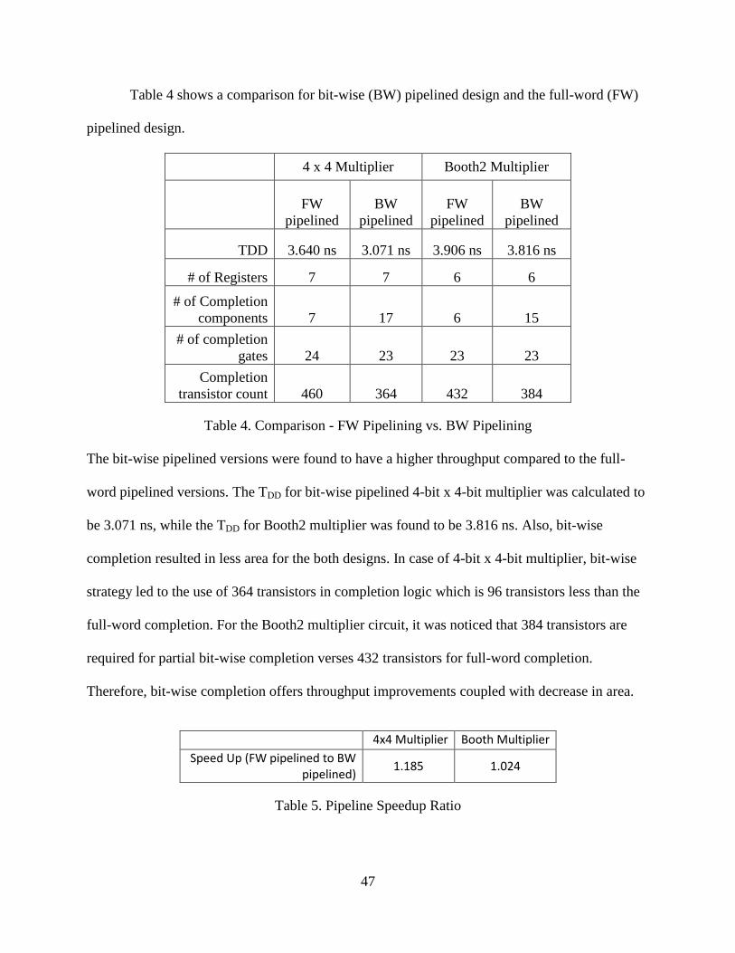
Table 4 shows a comparison for bit-wise (BW) pipelined design and the full-word (FW)
pipelined design.
4 x 4 Multiplier Booth2 Multiplier
FW
pipelined
BW
pipelined
FW
pipelined
BW
pipelined
TDD 3.640 ns 3.071 ns 3.906 ns 3.816 ns
# of Registers 7 7 6 6
# of Completion
components 7 17 6 15
# of completion
gates 24 23 23 23
Completion
transistor count 460 364 432 384
Table 4. Comparison - FW Pipelining vs. BW Pipelining
The bit-wise pipelined versions were found to have a higher throughput compared to the full-
word pipelined versions. The TDD for bit-wise pipelined 4-bit x 4-bit multiplier was calculated to
be 3.071 ns, while the TDD for Booth2 multiplier was found to be 3.816 ns. Also, bit-wise
completion resulted in less area for the both designs. In case of 4-bit x 4-bit multiplier, bit-wise
strategy led to the use of 364 transistors in completion logic which is 96 transistors less than the
full-word completion. For the Booth2 multiplier circuit, it was noticed that 384 transistors are
required for partial bit-wise completion verses 432 transistors for full-word completion.
Therefore, bit-wise completion offers throughput improvements coupled with decrease in area.
4x4 Multiplier Booth Multiplier
Speed Up (FW pipelined to BW pipelined)
1.185 1.024
Table 5. Pipeline Speedup Ratio

48
The speedup ratios shown in Table 5 indicate that bit-wise pipelined designs are faster than their
full-word pipelined versions, 1.185 times faster in case of 4 x 4 multiplier and 1.024 times faster
for Booth2 multiplier.

49
Chapter 8 Conclusion and Future Work
8.1 MTNCL CAD tool
An MTNCL CAD Tool (MCT) for converting Boolean circuits into their MTNCL
version was developed. It starts by processing the synthesized Boolean circuit, and then employs
equivalent MTNCL components instead of the standard Boolean gates. Next, it implements the
registration, completion, and sleep logic by applying FECII architecture. The algorithm then
performs logic minimization by eliminating signals/ports mapped to VDD and GND as required,
thereby reducing area. Then the MCT outputs the MTNCL version of the design as a hierarchical
VHDL model. MCT also has a programmable LUT and component declarations module to make
it easily adaptable to future MTNCL libraries, or different CAD tool suites.
MCT’s functionality was tested on a 4-bit x 4-bit multiplier circuit. The simulation results
proved the correctness of the algorithm. Further, MCT was tested on a larger circuit, 8-bit
Arithmetic Logic Unit (ALU) with eight operations, producing its MTNCL version in seconds.
The ALU’s simulation was accurate. This automated process for converting existing Boolean
circuits into its MTNCL equivalent will aid in reducing design time. Also, MCT has been
incorporated into the Synopsys CAD suite through a TCL script that calls a C-program. This
script is executed from within Design Vision’s user interface. As a design methodology similar
to that of synchronous circuits is utilized, it helps shorten the learning period for asynchronous
circuit design. The tool will assist and support wider adoption of asynchronous technologies like
MTNCL within the industry.
Currently, MCT supports only combinational circuits and is limited to handling specific number
of gates from the standard GTECH library. Future work includes expanding the scope of MCT so
that it supports the entire GTECH library and sequential circuits. This will enable MCT to tackle

50
more complex synchronous circuits and convert them into an equivalent MTNCL design with
ease. This will drastically help the asynchronous design landscape, as it will change the design-
from-scratch approach generally adopted for MTNCL asynchronous circuits. The designers
could easily convert synchronous circuits into MTNCL circuits, and employ them as modules for
quickly designing larger, more complex asynchronous circuits.
8.2 Automated Gate-Level Pipelining with Bit-Wise Completion Tool
An automated gate-level pipelining method for NULL Convention Logic (NCL) circuits
that implements bit-wise completion to achieve higher throughput was developed. AGLPBW’s
functionality was tested on a 4-bit x 4-bit NCL multiplier and an unsigned Booth2 multiplier.
The simulation results proved the correctness of the algorithm. The bit-wise pipelined designs
were found to be faster than their full-word pipelined versions. Additionally, bit-wise completion
offered comparatively less area.
Future work includes implementing an optimal AGLPBW by calculating completion and
combinational delays as per the bit-wise completion strategy and utilizing these delays to
partition and merge stages in the pipeline. It is also possible to merge the AGLP and AGLPBW
methods into a single tool that outputs the most optimized design, whether it is a bit-wise
pipelined or full-word pipelined design, for given user constraints on minimum throughput, area,
and latency. Further, AGLPBW could be expanded to include a process to apply NULL Cycle
Reduction (NCR) [11], to slower stages of the pipeline to further increase throughput for the
entire pipeline.

51
References
[1] "International Technology Roadmap for Semiconductors, 2011 Edition,"
http://www.itrs.net/Links/2011ITRS/Home2011.htm (available February 2013)
[2] Scott C. Smith and Jia Di, "Designing Asynchronous Circuits using NULL Convention Logic
(NCL)," Morgan & Claypool Publishers, July 2009.
[3] S. C. Smith, "Gate and throughput optimizations for null convention self-timed digital
circuits," pp. 154, 2001.
[4] K. M. Fant and S. A. Brandt, "NULL convention LogicTM: A complete and consistent logic
for asynchronous digital circuit synthesis," in Proceedings of International Conference on
Application Specific Systems, Architectures and Processors: ASAP '96, 1996, pp. 261-73.
[5] S. C. Smith, "Speedup of NULL convention digital circuits using NULL cycle reduction," J.
Syst. Archit., vol. 52, pp. 411-22, 07, 2006.
[6] G. E. Sobelman and K. Fant, "CMOS circuit design of threshold gates with hysteresis," in
ISCAS '98 Proceedings of the 1998 IEEE International Symposium on Circuits and Systems,
1998, pp. 61-4.
[7] S. C. Smith, R. F. DeMara, J. S. Yuan, D. Ferguson and D. Lamb, "Optimization of NULL
convention self-timed circuits," Integration, the VLSI Journal, vol. 37, pp. 135-65, 08, 2004.
[8] S. C. Smith, R. F. DeMara, J. S. Yuan, M. Hagedorn and D. Ferguson, "Delay-insensitive
gate-level pipelining," Integration, the VLSI Journal, vol. 30, pp. 103-31, 10, 2001.
[9] S. C. Smith, "Completion-Completeness for NULL Convention Digital Circuits Utilizing the
Bit-wise Completion Strategy," The 2003 International Conference on VLSI, pp. 143-149, June
2003.
[10] Venkat Satagopan, “Automated Pipelining Optimization, Energy Estimation, and DFT
Techniques for Asynchronous NULL Convention Circuits using Industry-Standard CAD Tools,”
University of Missouri – Rolla, May 2007.
[11] S. C. Smith, R. F. DeMara, J. S. Yuan, M. Hagedorn, and D. Ferguson, "Speedup of Delay-
Insensitive Digital Systems Using NULL Cycle Reduction," The 10th International Workshop on
Logic and Synthesis, pp. 185-189, June 2001.
[12] S. Mutoh, T. Douseki, Y. Matsuya, T. Aoki, S. Shigematsu, and J. Yamada, "1-V Power
Supply High-Speed Digital Circuit Technology with Multithreshold-Voltage CMOS," IEEE
Journal of Solid-State Circuits, Vol. 30/8, August 1995, pp. 847-854.

52
[13] J. T. Kao and A. P. Chandrakasan, "Dual-Threshold Voltage Techniques for Low-Power
Digital Circuits," IEEE Journal of Solid-State Circuits, Vol. 35/7, July 2000, pp. 1009-1018.
[14] P. Lakshmikanthan, K. Sahni, and A. Nunez, "Design of Ultra-Low Power Combinational
Standard Library Cells Using a Novel Leakage Reduction Methodology," IEEE International
SoC Conference, 2006.
[15] A. D. Bailey, J. Di, S. C. Smith, and H. A. Mantooth, "Ultra-Low Power Delay-Insensitive
Circuit Design," IEEE Midwest Symposium on Circuits and Systems, August 2008, pp. 503-506.
[16] A. D. Bailey, A. Al Zahrani, G. Fu, J. Di, and S. C. Smith, "Multi-Threshold Asynchronous
Circuit Design for Ultra-Low Power," Journal of Low Power Electronics, Vol. 4/3, December
2008, pp. 337-348.
[17] A. Alzahrani, A. D. Bailey, G. Fu, and J. Di, "Glitch-Free Design for Multi-Threshold
CMOS NCL Circuits," 2009 Great Lakes Symposium on VLSI, May 2009.
[18] S. C. Smith and J. Di, Designing Asynchronous Circuits using NULL Convention Logic
(NCL), Synthesis Lectures on Digital Circuits and Systems, Morgan & Claypool Publishers (doi:
10.2200/S00202ED1V01Y200907DCS023), Vol. 4/1, July 2009.
[19] L. Zhou, S. C. Smith, and J. Di, "Bit-Wise MTNCL: An Ultra-Low Power Bit-Wise
Pipelined Asynchronous Circuit Design Methodology," IEEE Midwest Symposium on Circuits
and Systems, August 2010, pp. 217-220.
[20] S. C. Smith, "Speedup of Self-Timed Digital Systems Using Early Completion," IEEE
Computer Society Annual Symposium on VLSI, April 2002, pp. 107-113.
[21] http://comp.uark.edu/~smithsco/CCLI_async.html(available February 2013).