Embed Size (px)
Citation preview

834766A1.CDR
C70 Capacitor Bank Protection and Control System
UR Series Instruction ManualC70 Revision: 7.0x
Manual P/N: 1601-9015-Y3 (GEK-113663B)
GE Digital Energy
650 Markland Street
Markham, Ontario
Canada L6C 0M1
Tel: +1 905 927 7070 Fax: +1 905 927 5098
Internet: http://www.GEDigitalEnergy.com
GE Multilin's Quality Management System is registered to ISO
9001:2008
QMI # 005094UL # A3775
*1601-9015-Y3*
LISTED
52TL
IND.CONT. EQ.
E83849
GEDigital Energy

Copyright © 2013 GE Multilin Inc. All rights reserved.
C70 Capacitor Bank Protection and Control System UR Series Instruction Manual revision 7.0x.
FlexLogic, FlexElement, FlexCurve, FlexAnalog, FlexInteger, FlexState, EnerVista, CyberSentry, HardFiber, Digital Energy, Multilin, and GE Multilin are trademarks or registered trademarks of GE Multilin Inc.
The contents of this manual are the property of GE Multilin Inc. This documentation is furnished on license and may not be reproduced in whole or in part without the permission of GE Multilin. The content of this manual is for informational use only and is subject to change without notice.Part number: 1601-9015-Y3 (April 2013)

GE Multilin C70 Capacitor Bank Protection and Control System iii
TABLE OF CONTENTS
0. BATTERY DISPOSAL 0.1 BATTERY DISPOSAL
1. GETTING STARTED 1.1 IMPORTANT PROCEDURES1.1.1 CAUTIONS AND WARNINGS ........................................................................... 1-11.1.2 INSPECTION CHECKLIST ................................................................................ 1-2
1.2 UR OVERVIEW1.2.1 INTRODUCTION TO THE UR ........................................................................... 1-31.2.2 HARDWARE ARCHITECTURE ......................................................................... 1-31.2.3 SOFTWARE ARCHITECTURE.......................................................................... 1-51.2.4 IMPORTANT CONCEPTS ................................................................................. 1-5
1.3 ENERVISTA UR SETUP SOFTWARE1.3.1 PC REQUIREMENTS ........................................................................................ 1-61.3.2 INSTALLATION.................................................................................................. 1-61.3.3 CONFIGURING THE C70 FOR SOFTWARE ACCESS .................................... 1-71.3.4 USING THE QUICK CONNECT FEATURE..................................................... 1-101.3.5 CONNECTING TO THE C70 RELAY .............................................................. 1-16
1.4 UR HARDWARE1.4.1 MOUNTING AND WIRING............................................................................... 1-171.4.2 COMMUNICATIONS........................................................................................ 1-171.4.3 FACEPLATE DISPLAY .................................................................................... 1-17
1.5 USING THE RELAY1.5.1 FACEPLATE KEYPAD..................................................................................... 1-181.5.2 MENU NAVIGATION ....................................................................................... 1-181.5.3 MENU HIERARCHY ........................................................................................ 1-181.5.4 RELAY ACTIVATION....................................................................................... 1-181.5.5 RELAY PASSWORDS ..................................................................................... 1-191.5.6 FLEXLOGIC CUSTOMIZATION ...................................................................... 1-191.5.7 COMMISSIONING ........................................................................................... 1-20
2. PRODUCT DESCRIPTION 2.1 INTRODUCTION2.1.1 OVERVIEW........................................................................................................ 2-12.1.2 ORDERING........................................................................................................ 2-32.1.3 REPLACEMENT MODULES ............................................................................. 2-6
2.2 SPECIFICATIONS2.2.1 PROTECTION ELEMENTS ............................................................................... 2-82.2.2 USER-PROGRAMMABLE ELEMENTS........................................................... 2-112.2.3 MONITORING.................................................................................................. 2-122.2.4 METERING ...................................................................................................... 2-122.2.5 INPUTS ............................................................................................................ 2-132.2.6 POWER SUPPLY ............................................................................................ 2-142.2.7 OUTPUTS ........................................................................................................ 2-142.2.8 COMMUNICATIONS........................................................................................ 2-162.2.9 INTER-RELAY COMMUNICATIONS............................................................... 2-162.2.10 ENVIRONMENTAL .......................................................................................... 2-172.2.11 TYPE TESTS ................................................................................................... 2-182.2.12 PRODUCTION TESTS .................................................................................... 2-182.2.13 APPROVALS ................................................................................................... 2-192.2.14 MAINTENANCE ............................................................................................... 2-19
3. HARDWARE 3.1 DESCRIPTION3.1.1 PANEL CUTOUT ............................................................................................... 3-13.1.2 MODULE WITHDRAWAL AND INSERTION ..................................................... 3-63.1.3 REAR TERMINAL LAYOUT............................................................................... 3-8
3.2 WIRING3.2.1 TYPICAL WIRING.............................................................................................. 3-9
iv C70 Capacitor Bank Protection and Control System GE Multilin
TABLE OF CONTENTS
3.2.2 DIELECTRIC STRENGTH................................................................................3-103.2.3 CONTROL POWER..........................................................................................3-103.2.4 CT/VT MODULES.............................................................................................3-113.2.5 PROCESS BUS MODULES .............................................................................3-133.2.6 CONTACT INPUTS AND OUTPUTS................................................................3-133.2.7 TRANSDUCER INPUTS/OUTPUTS.................................................................3-213.2.8 RS232 FACEPLATE PORT..............................................................................3-223.2.9 CPU COMMUNICATION PORTS.....................................................................3-223.2.10 IRIG-B...............................................................................................................3-25
3.3 DIRECT INPUT/OUTPUT COMMUNICATIONS3.3.1 DESCRIPTION .................................................................................................3-263.3.2 FIBER: LED AND ELED TRANSMITTERS ......................................................3-283.3.3 G.703 INTERFACE...........................................................................................3-293.3.4 RS422 INTERFACE .........................................................................................3-323.3.5 IEEE C37.94 INTERFACE................................................................................3-34
4. HUMAN INTERFACES 4.1 ENERVISTA UR SETUP INTERFACE4.1.1 INTRODUCTION ................................................................................................4-14.1.2 CREATING A SITE LIST ....................................................................................4-14.1.3 ENERVISTA UR SETUP OVERVIEW................................................................4-14.1.4 ENERVISTA UR SETUP MAIN WINDOW..........................................................4-3
4.2 EXTENDED ENERVISTA UR SETUP FEATURES4.2.1 SETTINGS TEMPLATES ...................................................................................4-44.2.2 SECURING AND LOCKING FLEXLOGIC EQUATIONS....................................4-84.2.3 SETTINGS FILE TRACEABILITY.....................................................................4-10
4.3 FACEPLATE INTERFACE4.3.1 FACEPLATE.....................................................................................................4-134.3.2 LED INDICATORS............................................................................................4-144.3.3 CUSTOM LABELING OF LEDS .......................................................................4-174.3.4 DISPLAY...........................................................................................................4-224.3.5 KEYPAD ...........................................................................................................4-224.3.6 BREAKER CONTROL ......................................................................................4-234.3.7 MENUS.............................................................................................................4-244.3.8 CHANGING SETTINGS ...................................................................................4-26
5. SETTINGS 5.1 OVERVIEW5.1.1 SETTINGS MENU ..............................................................................................5-15.1.2 INTRODUCTION TO ELEMENTS......................................................................5-45.1.3 INTRODUCTION TO AC SOURCES..................................................................5-5
5.2 PRODUCT SETUP5.2.1 SECURITY..........................................................................................................5-85.2.2 CYBERSENTRY SECURITY............................................................................5-125.2.3 DISPLAY PROPERTIES ..................................................................................5-195.2.4 CLEAR RELAY RECORDS ..............................................................................5-205.2.5 COMMUNICATIONS ........................................................................................5-215.2.6 MODBUS USER MAP ......................................................................................5-475.2.7 REAL TIME CLOCK .........................................................................................5-475.2.8 USER-PROGRAMMABLE FAULT REPORTS .................................................5-525.2.9 OSCILLOGRAPHY ...........................................................................................5-535.2.10 DATA LOGGER................................................................................................5-555.2.11 USER-PROGRAMMABLE LEDS .....................................................................5-575.2.12 USER-PROGRAMMABLE SELF TESTS .........................................................5-605.2.13 CONTROL PUSHBUTTONS ............................................................................5-615.2.14 USER-PROGRAMMABLE PUSHBUTTONS....................................................5-625.2.15 FLEX STATE PARAMETERS ..........................................................................5-675.2.16 USER-DEFINABLE DISPLAYS ........................................................................5-685.2.17 DIRECT INPUTS AND OUTPUTS....................................................................5-705.2.18 INSTALLATION ................................................................................................5-78

GE Multilin C70 Capacitor Bank Protection and Control System v
TABLE OF CONTENTS
5.3 REMOTE RESOURCES5.3.1 REMOTE RESOURCES CONFIGURATION................................................... 5-79
5.4 SYSTEM SETUP5.4.1 AC INPUTS ...................................................................................................... 5-805.4.2 POWER SYSTEM............................................................................................ 5-815.4.3 SIGNAL SOURCES ......................................................................................... 5-835.4.4 BREAKERS...................................................................................................... 5-865.4.5 DISCONNECT SWITCHES ............................................................................. 5-905.4.6 FLEXCURVES ................................................................................................. 5-93
5.5 FLEXLOGIC5.5.1 INTRODUCTION TO FLEXLOGIC ................................................................ 5-1005.5.2 FLEXLOGIC RULES ...................................................................................... 5-1115.5.3 FLEXLOGIC EVALUATION ........................................................................... 5-1115.5.4 FLEXLOGIC EXAMPLE ................................................................................. 5-1125.5.5 FLEXLOGIC EQUATION EDITOR................................................................. 5-1165.5.6 FLEXLOGIC TIMERS .................................................................................... 5-1165.5.7 FLEXELEMENTS........................................................................................... 5-1175.5.8 NON-VOLATILE LATCHES ........................................................................... 5-121
5.6 GROUPED ELEMENTS5.6.1 OVERVIEW.................................................................................................... 5-1225.6.2 SETTING GROUP ......................................................................................... 5-1225.6.3 BREAKER FAILURE...................................................................................... 5-1235.6.4 PHASE CURRENT ........................................................................................ 5-1325.6.5 NEUTRAL CURRENT.................................................................................... 5-1475.6.6 GROUND CURRENT..................................................................................... 5-1595.6.7 NEGATIVE SEQUENCE CURRENT ............................................................. 5-1615.6.8 VOLTAGE ELEMENTS.................................................................................. 5-166
5.7 CONTROL ELEMENTS5.7.1 OVERVIEW.................................................................................................... 5-1855.7.2 TRIP BUS....................................................................................................... 5-1855.7.3 SETTING GROUPS ....................................................................................... 5-1875.7.4 SELECTOR SWITCH..................................................................................... 5-1885.7.5 TIME OF DAY TIMERS.................................................................................. 5-1945.7.6 CAPACITOR CONTROL................................................................................ 5-1955.7.7 AUTOMATIC VOLTAGE REGULATOR......................................................... 5-2005.7.8 DIGITAL ELEMENTS..................................................................................... 5-2055.7.9 DIGITAL COUNTERS .................................................................................... 5-2085.7.10 MONITORING ELEMENTS ........................................................................... 5-210
5.8 INPUTS AND OUTPUTS5.8.1 CONTACT INPUTS........................................................................................ 5-2225.8.2 VIRTUAL INPUTS.......................................................................................... 5-2245.8.3 CONTACT OUTPUTS.................................................................................... 5-2255.8.4 VIRTUAL OUTPUTS...................................................................................... 5-2275.8.5 REMOTE DEVICES ....................................................................................... 5-2285.8.6 REMOTE INPUTS.......................................................................................... 5-2295.8.7 REMOTE DOUBLE-POINT STATUS INPUTS .............................................. 5-2305.8.8 REMOTE OUTPUTS...................................................................................... 5-2305.8.9 RESETTING................................................................................................... 5-2315.8.10 DIRECT INPUTS AND OUTPUTS................................................................. 5-2325.8.11 IEC 61850 GOOSE ANALOGS...................................................................... 5-2355.8.12 IEC 61850 GOOSE INTEGERS..................................................................... 5-236
5.9 TRANSDUCER INPUTS AND OUTPUTS5.9.1 DCMA INPUTS .............................................................................................. 5-2375.9.2 RTD INPUTS.................................................................................................. 5-2385.9.3 DCMA OUTPUTS .......................................................................................... 5-240
5.10 TESTING5.10.1 TEST MODE .................................................................................................. 5-2435.10.2 FORCE CONTACT INPUTS .......................................................................... 5-2445.10.3 FORCE CONTACT OUTPUTS ...................................................................... 5-245

vi C70 Capacitor Bank Protection and Control System GE Multilin
TABLE OF CONTENTS
6. ACTUAL VALUES 6.1 OVERVIEW6.1.1 ACTUAL VALUES MENU...................................................................................6-1
6.2 STATUS6.2.1 CONTACT INPUTS ............................................................................................6-36.2.2 VIRTUAL INPUTS ..............................................................................................6-36.2.3 REMOTE INPUTS ..............................................................................................6-36.2.4 REMOTE DOUBLE-POINT STATUS INPUTS ...................................................6-46.2.5 CONTACT OUTPUTS ........................................................................................6-46.2.6 VIRTUAL OUTPUTS ..........................................................................................6-46.2.7 REMOTE DEVICES............................................................................................6-56.2.8 DIGITAL COUNTERS.........................................................................................6-56.2.9 SELECTOR SWITCHES ....................................................................................6-66.2.10 TIME OF DAY TIMERS ......................................................................................6-66.2.11 FLEX STATES....................................................................................................6-66.2.12 ETHERNET ........................................................................................................6-66.2.13 REAL TIME CLOCK SYNCHRONIZING ............................................................6-76.2.14 DIRECT INPUTS ................................................................................................6-86.2.15 DIRECT DEVICES STATUS ..............................................................................6-86.2.16 IEC 61850 GOOSE INTEGERS .........................................................................6-96.2.17 REMAINING CONNECTION STATUS ...............................................................6-9
6.3 METERING6.3.1 METERING CONVENTIONS ...........................................................................6-106.3.2 SOURCES ........................................................................................................6-136.3.3 CAPACITOR CONTROL ..................................................................................6-176.3.4 CAPACITOR BANK ..........................................................................................6-186.3.5 TRACKING FREQUENCY................................................................................6-196.3.6 FLEXELEMENTS .............................................................................................6-196.3.7 IEC 61580 GOOSE ANALOG VALUES ...........................................................6-206.3.8 TRANSDUCER INPUTS/OUTPUTS.................................................................6-20
6.4 RECORDS6.4.1 USER-PROGRAMMABLE FAULT REPORTS .................................................6-216.4.2 EVENT RECORDS...........................................................................................6-216.4.3 OSCILLOGRAPHY ...........................................................................................6-216.4.4 DATA LOGGER................................................................................................6-22
6.5 PRODUCT INFORMATION6.5.1 MODEL INFORMATION...................................................................................6-236.5.2 FIRMWARE REVISIONS..................................................................................6-23
7. COMMANDS AND TARGETS
7.1 COMMANDS7.1.1 COMMANDS MENU...........................................................................................7-17.1.2 CAPACITOR BANK AUTOMATIC SETTINGS...................................................7-17.1.3 VIRTUAL INPUTS ..............................................................................................7-67.1.4 CLEAR RECORDS.............................................................................................7-67.1.5 SET DATE AND TIME ........................................................................................7-67.1.6 RELAY MAINTENANCE.....................................................................................7-77.1.7 SECURITY..........................................................................................................7-7
7.2 TARGETS7.2.1 TARGETS MENU ...............................................................................................7-97.2.2 TARGET MESSAGES ........................................................................................7-97.2.3 RELAY SELF-TESTS .........................................................................................7-9
8. SECURITY 8.1 USER ACCOUNTS8.1.1 OVERVIEW ........................................................................................................8-18.1.2 ENABLING THE SECURITY MANAGEMENT SYSTEM....................................8-18.1.3 ADDING A NEW USER ......................................................................................8-18.1.4 MODIFYING USER PRIVILEGES ......................................................................8-28.1.5 PASSWORD REQUIREMENTS.........................................................................8-3
GE Multilin C70 Capacitor Bank Protection and Control System vii
TABLE OF CONTENTS
8.2 CYBERSENTRY8.2.1 OVERVIEW........................................................................................................ 8-48.2.2 SECURITY MENU ............................................................................................. 8-6
9. THEORY OF OPERATION 9.1 OVERVIEW9.1.1 GENERAL OPERATION.................................................................................... 9-19.1.2 BANK PHASE OVERVOLTAGE (ANSI 59B)..................................................... 9-19.1.3 VOLTAGE DIFFERENTIAL (ANSI 87V) ............................................................ 9-39.1.4 COMPENSATED BANK NEUTRAL VOLTAGE UNBALANCE (ANSI 59NU).... 9-69.1.5 PHASE CURRENT UNBALANCE (ANSI 60P) ................................................ 9-109.1.6 NEUTRAL CURRENT UNBALANCE (ANSI 60N) ........................................... 9-12
10. APPLICATION OF SETTINGS
10.1 ARRANGEMENT OF SHUNT CAPACITOR BANKS10.1.1 OVERVIEW...................................................................................................... 10-110.1.2 EXTERNALLY FUSED CAPACITORS ............................................................ 10-110.1.3 INTERNALLY FUSED CAPACITORS ............................................................. 10-110.1.4 FUSELESS CAPACITORS .............................................................................. 10-210.1.5 UNFUSED CAPACITORS ............................................................................... 10-2
10.2 CONNECTIONS OF SHUNT CAPACITOR BANKS10.2.1 GROUNDED WYE-CONNECTED BANKS...................................................... 10-310.2.2 UNGROUNDED WYE-CONNECTED BANKS................................................. 10-310.2.3 DELTA-CONNECTED BANKS ........................................................................ 10-310.2.4 H-CONFIGURATION ....................................................................................... 10-310.2.5 TAPPED CONFIGURATION............................................................................ 10-310.2.6 SUMMARY....................................................................................................... 10-4
10.3 PROTECTION METHODS FOR CAPACITOR BANKS10.3.1 DESCRIPTION................................................................................................. 10-510.3.2 CAPACITOR UNBALANCE PROTECTION..................................................... 10-510.3.3 PROTECTION FOR RACK FAULTS (ARC-OVER WITHIN CAPACITOR BANK)
....................................................................................................................... 10-1010.3.4 OVERVOLTAGE ............................................................................................ 10-1010.3.5 OVERCURRENT ........................................................................................... 10-1110.3.6 LOSS OF BUS VOLTAGE ............................................................................. 10-11
10.4 SETTING EXAMPLE10.4.1 DESCRIPTION............................................................................................... 10-1210.4.2 VT AND CT SETUP ....................................................................................... 10-1210.4.3 SOURCE ASSIGNMENT ............................................................................... 10-1310.4.4 BANK UNBALANCE CALCULATIONS.......................................................... 10-1410.4.5 BANK VOLTAGE DIFFERENTIAL SETTINGS.............................................. 10-1610.4.6 BANK PHASE CURRENT UNBALANCE SETTINGS.................................... 10-1810.4.7 BANK PHASE OVERVOLTAGE SETTINGS ................................................. 10-1910.4.8 BANK PHASE UNDERVOLTAGE SETTINGS .............................................. 10-2010.4.9 BANK OVERCURRENT PROTECTION ........................................................ 10-21
A. FLEXANALOG AND FLEXINTEGER PARAMETERS
A.1 PARAMETER LISTSA.1.1 FLEXANALOG ITEMS .......................................................................................A-1A.1.2 FLEXINTEGER ITEMS ....................................................................................A-30
B. MODBUS COMMUNICATIONS
B.1 MODBUS RTU PROTOCOLB.1.1 INTRODUCTION................................................................................................B-1B.1.2 PHYSICAL LAYER.............................................................................................B-1B.1.3 DATA LINK LAYER............................................................................................B-1B.1.4 CRC-16 ALGORITHM........................................................................................B-2
viii C70 Capacitor Bank Protection and Control System GE Multilin
TABLE OF CONTENTS
B.2 MODBUS FUNCTION CODESB.2.1 SUPPORTED FUNCTION CODES ................................................................... B-3B.2.2 READ ACTUAL VALUES OR SETTINGS (FUNCTION CODE 03/04H) ........... B-3B.2.3 EXECUTE OPERATION (FUNCTION CODE 05H)........................................... B-4B.2.4 STORE SINGLE SETTING (FUNCTION CODE 06H)....................................... B-4B.2.5 STORE MULTIPLE SETTINGS (FUNCTION CODE 10H) ................................ B-5B.2.6 EXCEPTION RESPONSES............................................................................... B-5
B.3 FILE TRANSFERSB.3.1 OBTAINING RELAY FILES VIA MODBUS........................................................ B-6B.3.2 MODBUS PASSWORD OPERATION............................................................... B-7
B.4 MEMORY MAPPINGB.4.1 MODBUS MEMORY MAP ................................................................................. B-8B.4.2 DATA FORMATS............................................................................................. B-69
C. IEC 61850 COMMUNICATIONS
C.1 OVERVIEWC.1.1 INTRODUCTION ...............................................................................................C-1C.1.2 COMMUNICATION PROFILES.........................................................................C-1
C.2 SERVER DATA ORGANIZATIONC.2.1 OVERVIEW .......................................................................................................C-2C.2.2 GGIO1: DIGITAL STATUS VALUES .................................................................C-2C.2.3 GGIO2: DIGITAL CONTROL VALUES..............................................................C-2C.2.4 GGIO3: DIGITAL STATUS AND ANALOG VALUES FROM RECEIVED GOOSE
DATA .................................................................................................................C-2C.2.5 GGIO4: GENERIC ANALOG MEASURED VALUES.........................................C-2C.2.6 MMXU: ANALOG MEASURED VALUES ..........................................................C-3C.2.7 PROTECTION AND OTHER LOGICAL NODES...............................................C-3
C.3 SERVER FEATURES AND CONFIGURATIONC.3.1 BUFFERED/UNBUFFERED REPORTING........................................................C-5C.3.2 FILE TRANSFER...............................................................................................C-5C.3.3 TIMESTAMPS AND SCANNING.......................................................................C-5C.3.4 LOGICAL DEVICE NAME .................................................................................C-5C.3.5 LOCATION ........................................................................................................C-5C.3.6 LOGICAL NODE NAME PREFIXES..................................................................C-6C.3.7 CONNECTION TIMING .....................................................................................C-6C.3.8 NON-IEC 61850 DATA ......................................................................................C-6C.3.9 COMMUNICATION SOFTWARE UTILITIES.....................................................C-6
C.4 GENERIC SUBSTATION EVENT SERVICES: GSSE AND GOOSEC.4.1 OVERVIEW .......................................................................................................C-7C.4.2 GSSE CONFIGURATION..................................................................................C-7C.4.3 FIXED GOOSE ..................................................................................................C-7C.4.4 CONFIGURABLE GOOSE ................................................................................C-7C.4.5 ETHERNET MAC ADDRESS FOR GSSE/GOOSE ........................................C-10C.4.6 GSSE ID AND GOOSE ID SETTINGS............................................................C-10
C.5 IEC 61850 IMPLEMENTATION VIA ENERVISTA UR SETUPC.5.1 OVERVIEW .....................................................................................................C-11C.5.2 CONFIGURING IEC 61850 SETTINGS ..........................................................C-12C.5.3 ABOUT ICD FILES ..........................................................................................C-13C.5.4 CREATING AN ICD FILE WITH ENERVISTA UR SETUP..............................C-17C.5.5 ABOUT SCD FILES.........................................................................................C-17C.5.6 IMPORTING AN SCD FILE WITH ENERVISTA UR SETUP...........................C-20
C.6 ACSI CONFORMANCEC.6.1 ACSI BASIC CONFORMANCE STATEMENT ................................................C-22C.6.2 ACSI MODELS CONFORMANCE STATEMENT............................................C-22C.6.3 ACSI SERVICES CONFORMANCE STATEMENT.........................................C-23
C.7 LOGICAL NODESC.7.1 LOGICAL NODES TABLE ...............................................................................C-26

GE Multilin C70 Capacitor Bank Protection and Control System ix
TABLE OF CONTENTS
D. IEC 60870-5-104 COMMUNICATIONS
D.1 OVERVIEWD.1.1 INTEROPERABILITY DOCUMENT ...................................................................D-1D.1.2 POINT LIST........................................................................................................D-9
E. DNP COMMUNICATIONS E.1 DEVICE PROFILE DOCUMENTE.1.1 DNP V3.00 DEVICE PROFILE ..........................................................................E-1E.1.2 IMPLEMENTATION TABLE...............................................................................E-4
E.2 DNP POINT LISTSE.2.1 BINARY INPUT POINTS....................................................................................E-8E.2.2 BINARY AND CONTROL RELAY OUTPUT ......................................................E-9E.2.3 COUNTERS .....................................................................................................E-10E.2.4 ANALOG INPUTS ............................................................................................E-11
F. MISCELLANEOUS F.1 CHANGE NOTESF.1.1 REVISION HISTORY ......................................................................................... F-1F.1.2 CHANGES TO THE C70 MANUAL.................................................................... F-1
F.2 ABBREVIATIONSF.2.1 STANDARD ABBREVIATIONS ......................................................................... F-4
F.3 WARRANTYF.3.1 GE MULTILIN WARRANTY ............................................................................... F-7

x C70 Capacitor Bank Protection and Control System GE Multilin
TABLE OF CONTENTS
GE Multilin C70 Capacitor Bank Protection and Control System xi
0 BATTERY DISPOSAL 0.1 BATTERY DISPOSAL
00 BATTERY DISPOSAL 0.1BATTERY DISPOSAL
EN Battery DisposalThis product contains a battery that cannot be disposed of as unsorted municipal waste in the European Union. See the product documentation for specific battery information. The battery is marked with this symbol, which may include lettering to indicate cadmium (Cd), lead (Pb), or mercury (Hg). For proper recycling return the battery to your supplier or to a designated collection point. For more information see: www.recyclethis.info.
CS Nakládání s bateriemiTento produkt obsahuje baterie, které nemohou být zneškodněny v Evropské unii jako netříděný komunální odpadu. Viz dokumentace k produktu pro informace pro konkrétní baterie. Baterie je označena tímto symbolem, který může zahrnovat i uvedena písmena, kadmium (Cd), olovo (Pb), nebo rtuť (Hg). Pro správnou recyklaci baterií vraťte svémudodavateli nebo na určeném sběrném místě. Pro více informací viz: www.recyclethis.info.
DA Batteri affaldDette produkt indeholder et batteri som ikke kan bortskaffes sammen med almindeligt husholdningsaffald i Europa. Se produktinformation for specifikke informationer om batteriet. Batteriet er forsynet med indgraveret symboler for hvad batteriet indeholder: kadmium (Cd), bly (Pb) og kviksølv (Hg). Europæiske brugere af elektrisk udstyr skal aflevere kasserede produkter til genbrug eller til leverandøren. Yderligere oplysninger findes på webstedet www.recyclethis.info.
DE Entsorgung von BatterienDieses Produkt beinhaltet eine Batterie, die nicht als unsortierter städtischer Abfall in der europäischen Union entsorgt werden darf. Beachten Sie die spezifischen Batterie-informationen in der Produktdokumentation. Die Batterie ist mit diesem Symbol gekennzeichnet, welches auch Hinweise auf möglicherweise enthaltene Stoffe wie Kadmium (Cd), Blei (Pb) oder Quecksilber (Hektogramm) darstellt . Für die korrekte Wiederverwertung bringen Sie diese Batterie zu Ihrem lokalen Lieferanten zurück oder entsorgen Sie das Produkt an den gekennzeichneten Sammelstellen. Weitere Informationen hierzu finden Sie auf der folgenden Website: www.recyclethis.info.
EL Απόρριψη μπαταριώνΑυτό το προϊόν περιέχει μια μπαταρία που δεν πρέπει να απορρίπτεται σε δημόσια συστήματα απόρριψης στην Ευρωπαϊκή Κοινότητα. ∆είτε την τεκμηρίωση του προϊόντος για συγκεκριμένες πληροφορίες που αφορούν τη μπαταρία. Η μπαταρία είναι φέρει σήμανση με αυτό το σύμβολο, το οποίο μπορεί να περιλαμβάνει γράμματα για να δηλώσουν το κάδμιο (Cd), τον μόλυβδο (Pb), ή τον υδράργυρο (Hg). Για την κατάλληλη ανακύκλωση επιστρέψτε την μπαταρία στον προμηθευτή σας ή σε καθορισμένο σημείο συλλογής. Για περισσότερες πληροφορίες δείτε: www.recyclethis.info.
ES Eliminacion de bateriasEste producto contiene una batería que no se pueda eliminar como basura normal sin clasificar en la Unión Europea. Examine la documentación del producto para la información específica de la batería. La batería se marca con este símbolo, que puede incluir siglas para indicar el cadmio (Cd), el plomo (Pb), o el mercurio (Hg ). Para el reciclaje apropiado, devuelva este producto a su distribuidor ó deshágase de él en los puntos de reciclaje designados. Para mas información : wwwrecyclethis.info.
ET Patareide kõrvaldamineKäesolev toode sisaldab patareisid, mida Euroopa Liidus ei tohi kõrvaldada sorteerimata olmejäätmetena. Andmeid patareide kohta vaadake toote dokumentatsioonist. Patareid on märgistatud käesoleva sümboliga, millel võib olla kaadmiumi (Cd), pliid (Pb) või elavhõbedat (Hg) tähistavad tähed. Nõuetekohaseks ringlusse võtmiseks tagastage patarei tarnijale või kindlaksmääratud vastuvõtupunkti. Lisainformatsiooni saab Internetist aadressil: www.recyclethis.info.
FI Paristoje ja akkujen hävittäminenTuote sisältää pariston, jota ei saa hävittää Euroopan Unionin alueella talousjätteen mukana. Tarkista tuoteselosteesta tuotteen tiedot. Paristo on merkitty tällä symbolilla ja saattaa sisältää cadmiumia (Cd), lyijyä (Pb) tai elohopeaa (Hg). Oikean kierrätystavan varmistamiseksi palauta tuote paikalliselle jälleenmyyjälle tai palauta se paristojen keräyspisteeseen. Lisätietoja sivuilla www.recyclethis.info.
FR Élimination des pilesCe produit contient une batterie qui ne peuvent être éliminés comme déchets municipaux non triés dans l'Union européenne. Voir la documentation du produit au niveau des renseignements sur la pile. La batterie est marqué de ce symbole, qui comprennent les indications cadmium (Cd), plomb (Pb), ou mercure (Hg). Pour le recyclage, retourner la batterie à votre fournisseur ou à un point de collecte. Pour plus d'informations, voir: www.recyclethis.info.
HU Akkumulátor hulladék kezeléseEzen termék akkumulátort tartalmaz, amely az Európai Unión belül csak a kijelölt módon és helyen dobható ki. A terméken illetve a mellékelt ismertetőn olvasható a kadmium (Cd), ólom (Pb) vagy higany (Hg) tartalomra utaló betűjelzés. A hulladék akkumulátor leadható a termék forgalmazójánál új akkumulátor vásárlásakor, vagy a kijelölt elektronikai hulladékudvarokban. További információ a www.recyclethis.info oldalon.

xii C70 Capacitor Bank Protection and Control System GE Multilin
0.1 BATTERY DISPOSAL 0 BATTERY DISPOSAL
0IT Smaltimento batterieQuesto prodotto contiene una batteria che non può essere smaltita nei comuni contenitori per lo smaltimento rifiuti, nell' Unione Europea. Controllate la documentazione del prodotto per le informazioni specifiche sulla batteria. La batteria è contrassegnata con questo simbolo e può includere alcuni caratteri ad indicare la presenza di cadmio (Cd), piombo (Pb) oppure mercurio (Hg). Per il corretto smaltimento, potete restituirli al vostro fornitore locale, oppure rivolgervi e consegnarli presso i centri di raccolta preposti. Per maggiori informazioni vedere: ww.recyclethis.info.
LT Baterijų šalinimasŠios įrangos sudėtyje yra baterijų, kurias draudžiama šalinti Europos Sąjungos viešose nerūšiuotų atliekų šalinimo sistemose. Informaciją apie baterijas galite rasti įrangos techninėje dokumentacijoje. Baterijos žymimos šiuo simboliu, papildomai gali būti nurodoma kad baterijų sudėtyje yra kadmio (Cd), švino (Pb) ar gyvsidabrio (Hg). Eksploatavimui nebetinkamas baterijas pristatykite į tam skirtas surinkimo vietas arba grąžinkite jas tiesioginiam tiekėjui, kad jos būtų tinkamai utilizuotos. Daugiau informacijos rasite šioje interneto svetainėje: www.recyclethis.info.
LV Bateriju likvidēšanaŠis produkts satur bateriju vai akumulatoru, kuru nedrīkst izmest Eiropas Savienībā esošajās sadzīves atkritumu sistēmās. Sk. produkta dokumentācijā, kur ir norādīta konkrēta informācija par bateriju vai akumulatoru. Baterijas vai akumulatora marķējumā ir šis simbols, kas var ietvert burtus, kuri norāda kadmiju (Cd), svinu (Pb) vai dzīvsudrabu (Hg). Pēc ekspluatācijas laika beigām baterijas vai akumulatori jānodod piegādātājam vai specializētā bateriju savākšanas vietā. Sīkāku informāciju var iegūt vietnē: www.recyclethis.info.
NL Verwijderen van baterijenDit product bevat een batterij welke niet kan verwijdert worden via de gemeentelijke huisvuilscheiding in de Europese Gemeenschap. Gelieve de product documentatie te controleren voor specifieke batterij informatie. De batterijen met deze label kunnen volgende indictaies bevatten cadium (Cd), lood (Pb) of kwik (Hg). Voor correcte vorm van kringloop, geef je de producten terug aan jou locale leverancier of geef het af aan een gespecialiseerde verzamelpunt. Meer informatie vindt u op de volgende website: www.recyclethis.info.
NO Retur av batteriDette produkt inneholder et batteri som ikke kan kastes med usortert kommunalt søppel i den Europeiske Unionen. Se produktdokumentasjonen for spesifikk batteriinformasjon. Batteriet er merket med dette symbolet som kan inkludere symboler for å indikere at kadmium (Cd), bly (Pb), eller kvikksølv (Hg) forekommer. Returner batteriet til leverandøren din eller til et dedikert oppsamlingspunkt for korrekt gjenvinning. For mer informasjon se: www.recyclethis.info.
PL Pozbywanie się zużytych bateriiTen produkt zawiera baterie, które w Unii Europejskiej mogą być usuwane tylko jako posegregowane odpady komunalne. Dokładne informacje dotyczące użytych baterii znajdują się w dokumentacji produktu. Baterie oznaczone tym symbolem mogą zawierać dodatkowe oznaczenia literowe wskazujące na zawartość kadmu (Cd), ołowiu (Pb) lub rtęci (Hg). Dla zapewnienia właściwej utylizacji, należy zwrócić baterie do dostawcy albo do wyznaczonego punktu zbiórki. Więcej informacji można znaleźć na stronie internetowej www.recyclethis.info.
PT Eliminação de BateriasEste produto contêm uma bateria que não pode ser considerado lixo municipal na União Europeia. Consulte a documentação do produto para obter informação específica da bateria. A bateria é identificada por meio de este símbolo, que pode incluir a rotulação para indicar o cádmio (Cd), chumbo (Pb), ou o mercúrio (hg). Para uma reciclagem apropriada envie a bateria para o seu fornecedor ou para um ponto de recolha designado. Para mais informação veja: www.recyclethis.info.
RU Утилизация батарейСогласно европейской директиве об отходах электрического и электронного оборудования, продукты, содержащие батареи, нельзя утилизировать как обычные отходы на территории ЕС. Более подробную информацию вы найдете в документации к продукту. На этом символе могут присутствовать буквы, которые означают, что батарея собержит кадмий (Cd), свинец (Pb) или ртуть (Hg). Для надлежащей утилизации по окончании срока эксплуатации пользователь должен возвратить батареи локальному поставщику или сдать в специальный пункт приема. Подробности можно найти на веб-сайте: www.recyclethis.info.
SK Zaobchádzanie s batériamiTento produkt obsahuje batériu, s ktorou sa v Európskej únii nesmie nakladať ako s netriedeným komunálnym odpadom. Dokumentácia k produktu obsahuje špecifické informácie o batérii. Batéria je označená týmto symbolom, ktorý môže obsahovať písmená na označenie kadmia (Cd), olova (Pb), alebo ortuti (Hg). Na správnu recykláciu vráťte batériu vášmu lokálnemu dodávateľovi alebo na určené zberné miesto. Pre viac informácii pozrite: www.recyclethis.info.
SL Odlaganje baterijTa izdelek vsebuje baterijo, ki je v Evropski uniji ni dovoljeno odstranjevati kot nesortiran komunalni odpadek. Za posebne informacije o bateriji glejte dokumentacijo izdelka. Baterija je označena s tem simbolom, ki lahko vključuje napise, ki označujejo kadmij (Cd), svinec (Pb) ali živo srebro (Hg). Za ustrezno recikliranje baterijo vrnite dobavitelju ali jo odstranite na določenem zbirališču. Za več informacij obiščite spletno stran: www.recyclethis.info.
SV Kassering av batteriDenna produkt innehåller ett batteri som inte får kastas i allmänna sophanteringssytem inom den europeiska unionen. Se produktdokumentationen för specifik batteriinformation. Batteriet är märkt med denna symbol, vilket kan innebära att det innehåller kadmium (Cd), bly (Pb) eller kvicksilver (Hg). För korrekt återvinning skall batteriet returneras till leverantören eller till en därför avsedd deponering. För mer information, se: www.recyclethis.info.
GE Multilin C70 Capacitor Bank Protection and Control System xiii
0 BATTERY DISPOSAL 0.1 BATTERY DISPOSAL
0TR Pil Geri DönüşümüBu ürün Avrupa Birliği genel atık sistemlerine atılmaması gereken pil içermektedir. Daha detaylı pil bilgisi için ürünün kataloğunu inceleyiniz. Bu sembolle işaretlenmiş piller Kadmiyum(Cd), Kurşun(Pb) ya da Civa(Hg) içerebilir. Doğru geri dönüşüm için ürünü yerel tedarikçinize geri veriniz ya da özel işaretlenmiş toplama noktlarına atınız. Daha fazla bilgi için: www.recyclethis.info.
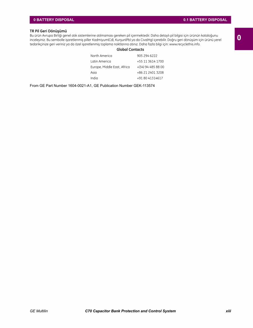
Global Contacts
From GE Part Number 1604-0021-A1, GE Publication Number GEK-113574
North America 905 294 6222
Latin America +55 11 3614 1700
Europe, Middle East, Africa +(34) 94 485 88 00
Asia +86 21 2401 3208
India +91 80 41314617

xiv C70 Capacitor Bank Protection and Control System GE Multilin
0.1 BATTERY DISPOSAL 0 BATTERY DISPOSAL
0

GE Multilin C70 Capacitor Bank Protection and Control System 1-1
1 GETTING STARTED 1.1 IMPORTANT PROCEDURES
11 GETTING STARTED 1.1IMPORTANT PROCEDURES
Read this chapter to help guide you through the initial setup of your new C70 Capacitor Bank Protection and ControlSystem.
1.1.1 CAUTIONS AND WARNINGS
Before attempting to install or use the device, review all safety indicators in this document to help prevent injury, equipmentdamage, or downtime.
The following safety and equipment symbols are used in this document.
Indicates a hazardous situation which, if not avoided, will result in death or serious injury.
Indicates a hazardous situation which, if not avoided, could result in death or serious injury.
Indicates a hazardous situation which, if not avoided, could result in minor or moderateinjury.
Indicates practices not related to personal injury.
a) GENERAL CAUTIONS AND WARNINGS
The following general safety precautions and warnings apply.
Ensure that all connections to the product are correct so as to avoid accidental risk of shockand/or fire, for example such as can arise from high voltage connected to low voltage termi-nals.
Follow the requirements of this manual, including adequate wiring size and type, terminal torque settings, voltage,current magnitudes applied, and adequate isolation/clearance in external wiring from high to low voltage circuits.
Use the device only for its intended purpose and application.
Ensure that all ground paths are uncompromised for safety purposes during device operation and service.
Ensure that the control power applied to the device, the AC current, and voltage input match the ratings specifiedon the relay nameplate. Do not apply current or voltage in excess of the specified limits.
Only qualified personnel are to operate the device. Such personnel must be thoroughly familiar with all safety cau-tions and warnings in this manual and with applicable country, regional, utility, and plant safety regulations.
Hazardous voltages can exist in the power supply and at the device connection to current transformers, voltagetransformers, control, and test circuit terminals. Make sure all sources of such voltages are isolated prior toattempting work on the device.
Hazardous voltages can exist when opening the secondary circuits of live current transformers. Make sure thatcurrent transformer secondary circuits are shorted out before making or removing any connection to the currenttransformer (CT) input terminals of the device.
For tests with secondary test equipment, ensure that no other sources of voltages or currents are connected tosuch equipment and that trip and close commands to the circuit breakers or other switching apparatus are iso-lated, unless this is required by the test procedure and is specified by appropriate utility/plant procedure.
When the device is used to control primary equipment, such as circuit breakers, isolators, and other switchingapparatus, all control circuits from the device to the primary equipment must be isolated while personnel areworking on or around this primary equipment to prevent any inadvertent command from this device.
Use an external disconnect to isolate the mains voltage supply.
LED transmitters are classified as IEC 60825-1 Accessible Emission Limit (AEL) Class 1M.Class 1M devices are considered safe to the unaided eye. Do not view directly with opticalinstruments.
This product is rated to Class A emissions levels and is to be used in Utility, Substation Industrialenvironments. Not to be used near electronic devices rated for Class B levels.

1-2 C70 Capacitor Bank Protection and Control System GE Multilin
1.1 IMPORTANT PROCEDURES 1 GETTING STARTED
11.1.2 INSPECTION CHECKLIST
1. Open the relay packaging and inspect the unit for physical damage.
2. View the rear nameplate and verify that the correct model has been ordered and delivered.
Figure 1–1: REAR NAMEPLATE (EXAMPLE)
3. Ensure that the following items are included:
• Instruction manual (if ordered)
• GE EnerVista™ CD (includes the EnerVista UR Setup software and manuals in PDF format)
• Mounting screws
For product information, instruction manual updates, and the latest software updates, visit the GE Digital Energy website athttp://www.gedigitalenergy.com.
If there is any noticeable physical damage, or any of the contents listed are missing, please contact GE DigitalEnergy immediately.
GE DIGITAL ENERGY CONTACT INFORMATION AND CALL CENTER FOR PRODUCT SUPPORT:
GE Digital Energy650 Markland StreetMarkham, OntarioCanada L6C 0M1
TELEPHONE: Worldwide +1 905 927 7070Europe/Middle East/Africa +34 94 4854 88 54North America toll-free 1 800 547 8629
FAX: +1 905 927 5098EMAIL: [email protected] PAGE: http://www.gedigitalenergy.com/multilin
NOTE

GE Multilin C70 Capacitor Bank Protection and Control System 1-3
1 GETTING STARTED 1.2 UR OVERVIEW
11.2UR OVERVIEW 1.2.1 INTRODUCTION TO THE UR
Historically, substation protection, control, and metering functions were performed with electromechanical equipment. Thisequipment was gradually replaced by analog equipment, most of which emulated the single-function approach of their elec-tromechanical precursors. Both technologies required expensive cabling and auxiliary equipment to produce functioningsystems.
Recently, digital electronic equipment has begun to provide protection, control, and metering functions. Initially, this equip-ment was either single function or had very limited multifunction capability, and it did not significantly reduce the cabling andauxiliary equipment required. However, recent digital relays are multifunctional, reducing cabling and auxiliaries signifi-cantly. These devices also transfer data to central control facilities and software using electronic communications. Thefunctions performed have become so broad that many users now prefer the term Intelligent Electronic Device (IED).
It is obvious to station designers that the amount of cabling and auxiliary equipment installed can be even further reduced,to 20% to 70% of levels common in 1990, and achieve large cost reductions. This requires placing even more functionswithin the IEDs.
Users of power equipment are also interested in reducing cost by improving power quality and personnel productivity, andin increasing system reliability and efficiency. These objectives are realized through software that is used to perform func-tions at both the station and supervisory levels. The use of these systems is growing rapidly.
High-speed communication is required to meet the data transfer rates required by modern automatic control and monitoringsystems. Very high speed communications are required to perform protection signaling with a performance target responsetime for a command signal between two IEDs, from transmission to reception, of less than 3 milliseconds. This has beenestablished by the IEC 61850 standard.
IEDs with such capabilities also provide significantly more power system data than was available, enhanced operations andmaintenance, and permit the use of adaptive system configuration for protection and control systems. This new generationof equipment is easily incorporated into automation systems, at both the station and enterprise levels. The GE Multilin Uni-versal Relay (UR) series meets these goals.
1.2.2 HARDWARE ARCHITECTURE
a) UR BASIC DESIGN
The UR is a digital-based device containing a central processing unit (CPU) that handles multiple types of input and outputsignals. The UR device can communicate over a local area network (LAN) with an operator interface, a programmingdevice, or another UR device.
Figure 1–2: UR CONCEPT BLOCK DIAGRAM
The CPU module contains firmware that provides protection elements in the form of logic algorithms, as well as program-mable logic gates, timers, and latches for control features.

1-4 C70 Capacitor Bank Protection and Control System GE Multilin
1.2 UR OVERVIEW 1 GETTING STARTED
1Input elements accept a variety of analog or digital signals from the field. The UR isolates and converts these signals intologic signals used by the relay.
Output elements convert and isolate the logic signals generated by the relay into digital or analog signals that can be usedto control field devices.
b) UR SIGNAL TYPES
The contact inputs and outputs are digital signals associated with connections to hard-wired contacts. Both ‘wet’ and ‘dry’contacts are supported.
The virtual inputs and outputs are digital signals associated with UR-series internal logic signals. Virtual inputs includesignals generated by the local user interface. The virtual outputs are outputs of FlexLogic™ equations used to customizethe device. Virtual outputs can also serve as virtual inputs to FlexLogic equations.
The analog inputs and outputs are signals that are associated with transducers, such as Resistance Temperature Detec-tors (RTDs).
The CT and VT inputs refer to analog current transformer and voltage transformer signals used to monitor AC power lines.The UR-series relays support 1 A and 5 A CTs.
The remote inputs and outputs provide a means of sharing digital point state information between remote UR-seriesdevices. The remote outputs interface to the remote inputs of other UR-series devices. Remote outputs are FlexLogic oper-ands inserted into IEC 61850 GSSE and GOOSE messages.
The direct inputs and outputs provide a means of sharing digital point states between a number of UR-series IEDs over adedicated fiber (single or multimode), RS422, or G.703 interface. No switching equipment is required as the IEDs are con-nected directly in a ring or redundant (dual) ring configuration. This feature is optimized for speed and intended for pilot-aided schemes, distributed logic applications, or the extension of the input/output capabilities of a single relay chassis.
c) UR SCAN OPERATION
The UR-series devices operate in a cyclic scan fashion. The device reads the inputs into an input status table, solves thelogic program (FlexLogic equation), and then sets each output to the appropriate state in an output status table. Any result-ing task execution is priority interrupt-driven.
Figure 1–3: UR-SERIES SCAN OPERATION

GE Multilin C70 Capacitor Bank Protection and Control System 1-5
1 GETTING STARTED 1.2 UR OVERVIEW
11.2.3 SOFTWARE ARCHITECTURE
The firmware (software embedded in the relay) is designed in functional modules that can be installed in any relay asrequired. This is achieved with object-oriented design and programming (OOD/OOP) techniques.
Object-oriented techniques involve the use of objects and classes. An object is defined as “a logical entity that containsboth data and code that manipulates that data”. A class is the generalized form of similar objects. By using this concept,one can create a protection class with the protection elements as objects of the class, such as time overcurrent, instanta-neous overcurrent, current differential, undervoltage, overvoltage, underfrequency, and distance. These objects representcompletely self-contained software modules. The same object-class concept can be used for metering, input/output control,software interface, communications, or any functional entity in the system.
Employing OOD/OOP in the software architecture of the C70 achieves the same features as the hardware architecture:modularity, scalability, and flexibility. The application software for any UR-series device (for example, feeder protection,transformer protection, distance protection) is constructed by combining objects from the various functional classes. Thisresults in a common interface across the UR series.
1.2.4 IMPORTANT CONCEPTS
As described above, the architecture of the UR-series relays differ from previous devices. To achieve a general understand-ing of this device, some sections of Chapter 5 are quite helpful. The most important functions of the relay are contained in“elements”. A description of the UR-series elements can be found in the Introduction to elements section in chapter 5.Examples of simple elements, and some of the organization of this manual, can be found in the Control elements section ofchapter 5. An explanation of the use of inputs from CTs and VTs is in the Introduction to AC sources section in chapter 5. Adescription of how digital signals are used and routed within the relay is contained in the Introduction to FlexLogic section inchapter 5.

1-6 C70 Capacitor Bank Protection and Control System GE Multilin
1.3 ENERVISTA UR SETUP SOFTWARE 1 GETTING STARTED
11.3ENERVISTA UR SETUP SOFTWARE 1.3.1 PC REQUIREMENTS
The faceplate keypad and display or the EnerVista UR Setup software can be used to communicate with the relay. TheEnerVista UR Setup software interface is the preferred method to edit settings and view actual values because the com-puter monitor can display more information.
The following minimum requirements must be met for the EnerVista UR Setup software to properly operate on a computer:
• Pentium class or higher processor (Pentium II 300 MHz or higher recommended)
• Windows 95, 98, 98SE, ME, NT 4.0 (Service Pack 4 or higher), 2000, XP
• Internet Explorer 4.0 or higher
• 128 MB of RAM (256 MB recommended)
• 200 MB of available space on system drive and 200 MB of available space on installation drive
• Video capable of displaying 800 x 600 or higher in high-color mode (16-bit color)
• RS232 and/or Ethernet port for communications to the relay
The following qualified modems have been tested to be compliant with the C70 and the EnerVista UR Setup software:
• US Robotics external 56K FaxModem 5686
• US Robotics external Sportster 56K X2
• PCTEL 2304WT V.92 MDC internal modem
1.3.2 INSTALLATION
After ensuring the minimum requirements for using EnerVista UR Setup are met (previous section), install the EnerVista URSetup from the GE EnerVista CD. Or download the UR EnerVista software from http://www.gedigitalenergy.com/multilinand install it.
1. Insert the GE EnerVista CD into your CD-ROM drive.
2. Click the Install Now button and follow the installation instructions to install the EnerVista software.
3. When installation is complete, start the EnerVista Launchpad application.
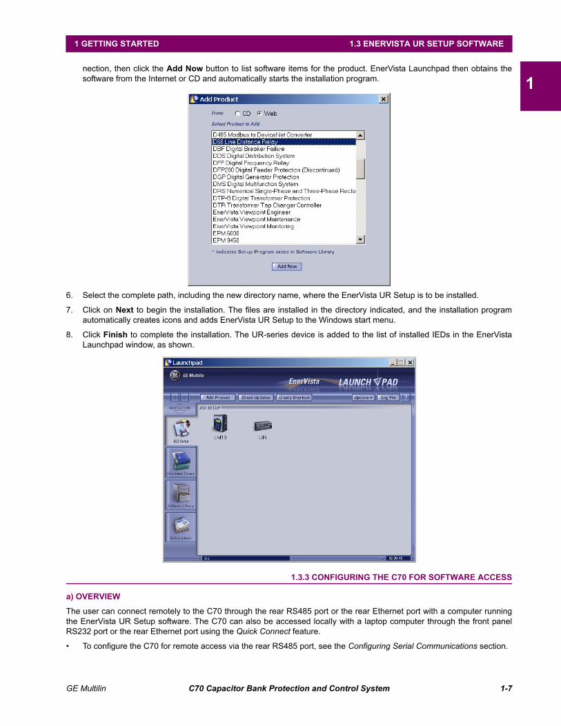
4. Click the IED Setup section of the Launch Pad window.
5. In the EnerVista Launch Pad window, click the Add Product button and select the appropriate product, shown as fol-lows. Select the "Web" option to ensure the most recent software release, or select "CD" if you do not have a web con-
GE Multilin C70 Capacitor Bank Protection and Control System 1-7
1 GETTING STARTED 1.3 ENERVISTA UR SETUP SOFTWARE
1nection, then click the Add Now button to list software items for the product. EnerVista Launchpad then obtains thesoftware from the Internet or CD and automatically starts the installation program.
6. Select the complete path, including the new directory name, where the EnerVista UR Setup is to be installed.
7. Click on Next to begin the installation. The files are installed in the directory indicated, and the installation programautomatically creates icons and adds EnerVista UR Setup to the Windows start menu.
8. Click Finish to complete the installation. The UR-series device is added to the list of installed IEDs in the EnerVistaLaunchpad window, as shown.
1.3.3 CONFIGURING THE C70 FOR SOFTWARE ACCESS
a) OVERVIEW
The user can connect remotely to the C70 through the rear RS485 port or the rear Ethernet port with a computer runningthe EnerVista UR Setup software. The C70 can also be accessed locally with a laptop computer through the front panelRS232 port or the rear Ethernet port using the Quick Connect feature.
• To configure the C70 for remote access via the rear RS485 port, see the Configuring Serial Communications section.

1-8 C70 Capacitor Bank Protection and Control System GE Multilin
1.3 ENERVISTA UR SETUP SOFTWARE 1 GETTING STARTED
1• To configure the C70 for remote access via the rear Ethernet port, see the Configuring Ethernet Communications sec-
tion. An Ethernet module must be specified at the time of ordering.
• To configure the C70 for local access with a laptop through either the front RS232 port or rear Ethernet port, see theUsing the Quick Connect Feature section.
b) CONFIGURING SERIAL COMMUNICATIONS
Before starting, verify that the serial cable is properly connected to the RS485 terminal on the back of the device. The face-plate RS232 port is intended for local use and is not described in this section; see the Using the Quick Connect Featuresection.
A GE Multilin F485 converter (or compatible RS232-to-RS485 converter) is required. Refer to the F485 instruction manualfor details.
1. Verify that the latest version of the EnerVista UR Setup software is installed (available from the GE EnerVista CD oronline from http://www.gedigitalenergy.com/multilin). See the Software Installation section if not already installed.
2. Select the “UR” device from the EnerVista Launchpad to start EnerVista UR Setup.
3. Click the Device Setup button to open the Device Setup window and click the Add Site button to define a new site.
4. Enter a site name in the “Site Name” field. Optionally add a short description of the site along with the display order ofdevices defined for the site. In this example, we use “Location 1” as the site name. Click the OK button when complete.The new site appears in the upper-left list in the EnerVista UR Setup window.
5. Click the Device Setup button, then select the new site to re-open the Device Setup window.
6. Click the Add Device button to define the new device.
7. Enter a name in the "Device Name” field and a description (optional) of the site.
8. Select “Serial” from the Interface drop-down list. This displays a number of interface parameters that must be enteredfor serial communications.
Figure 1–4: CONFIGURING SERIAL COMMUNICATIONS
9. Enter the relay slave address, COM port, baud rate, and parity settings from the SETTINGS PRODUCT SETUP COM-
MUNICATIONS SERIAL PORTS menu in their respective fields.

GE Multilin C70 Capacitor Bank Protection and Control System 1-9
1 GETTING STARTED 1.3 ENERVISTA UR SETUP SOFTWARE
110. Click the Read Order Code button to connect to the C70 device and upload the order code. If a communications error
occurs, ensure that the EnerVista UR Setup serial communications values entered in the previous step correspond tothe relay setting values.
11. Click the OK button when the relay order code has been received. The new device is added to the Site List window (orOnline window) located in the top left corner of the main EnerVista UR Setup window.
The device has now been configured for RS232 communications. Proceed to the Connecting to the C70 section to begincommunication.
c) CONFIGURING ETHERNET COMMUNICATIONS
Before starting, verify that the Ethernet network cable is properly connected to the Ethernet port on the back of the relay. Tosetup the relay for Ethernet communications, you define a Site, then add the relay as a Device at that site.The computerand UR device must be on the same subnet.
1. Verify that the latest version of the EnerVista UR Setup software is installed (available from the GE EnerVista CD oronline from http://www.gedigitalenergy.com/multilin). See the Software Installation section for installation details.
2. Select the “UR” device from the EnerVista Launchpad to start EnerVista UR Setup.
3. Click the Device Setup button to open the Device Setup window, then click the Add Site button to define a new site.
4. Enter the desired site name in the “Site Name” field. If desired, a short description of site can also be entered alongwith the display order of devices defined for the site. In this example, we use “Location 2” as the site name. Click theOK button when complete.
5. The new site appears in the upper-left list in the EnerVista UR Setup window. Click the Device Setup button thenselect the new site to re-open the Device Setup window.
6. Click the Add Device button to define the new device.
7. Enter the desired name in the “Device Name” field and a description (optional) of the site.
8. Select “Ethernet” from the Interface drop-down list. This displays a number of interface parameters that must beentered for proper Ethernet functionality.
Figure 1–5: CONFIGURING ETHERNET COMMUNICATIONS
9. Enter the relay IP address specified in the SETTINGS PRODUCT SETUP COMMUNICATIONS NETWORK IP
ADDRESS in the “IP Address” field.

1-10 C70 Capacitor Bank Protection and Control System GE Multilin
1.3 ENERVISTA UR SETUP SOFTWARE 1 GETTING STARTED
110. Enter the relay slave address and Modbus port address values from the respective settings in the SETTINGS PROD-
UCT SETUP COMMUNICATIONS MODBUS PROTOCOL menu.
11. Click the Read Order Code button to connect to the C70 device and upload the order code. If an communicationserror occurs, ensure that the three EnerVista UR Setup values entered in the previous steps correspond to the relaysetting values.
12. Click OK when the relay order code has been received. The new device is added to the Site List window (or Onlinewindow) located in the top left corner of the main EnerVista UR Setup window.
The Site Device has now been configured for Ethernet communications. Proceed to the Connecting to the C70 section tobegin communications.
1.3.4 USING THE QUICK CONNECT FEATURE
a) USING QUICK CONNECT VIA THE FRONT PANEL RS232 PORT
Before starting, verify that the serial cable is properly connected from the computer to the front panel RS232 port with astraight-through 9-pin to 9-pin RS232 cable.
1. Verify that the latest version of the EnerVista UR Setup software is installed (available from the GE EnerVista CD oronline from http://www.gedigitalenergy.com/multilin). See the Software Installation section if not already installed.
2. Select the “UR” device from the EnerVista Launchpad to start EnerVista UR Setup.
3. Click the Quick Connect button to open the Quick Connect dialog box.
4. Select the Serial interface and the correct COM Port, then click Connect.
5. The EnerVista UR Setup software creates a site named “Quick Connect” with a corresponding device also named“Quick Connect” and displays them at the upper-left of the screen. Expand the sections to view data directly from theC70 device.
Each time that the EnerVista UR Setup software is initialized, click the Quick Connect button to establish direct communi-cations to the C70 device. This ensures that configuration of the EnerVista UR Setup software matches the C70 modelnumber.
b) USING QUICK CONNECT VIA THE REAR ETHERNET PORTS
To use the Quick Connect feature to access the C70 from a computer through Ethernet, first assign an IP address to therelay from the front panel keyboard.
1. Press the MENU key until the SETTINGS menu displays.
2. Navigate to the SETTINGS PRODUCT SETUP COMMUNICATIONS NETWORK IP ADDRESS setting.
3. Enter an IP address, for example “1.1.1.1,” and select the ENTER key to save the value.
4. In the same menu, select the SUBNET IP MASK setting.
5. Enter a subnet IP address, for example “255.0.0.0,” and press the ENTER key to save the value.

GE Multilin C70 Capacitor Bank Protection and Control System 1-11
1 GETTING STARTED 1.3 ENERVISTA UR SETUP SOFTWARE
1Next, use an Ethernet cross-over cable to connect the computer to the rear Ethernet port. In case you need it, the figureshows the pinout for an Ethernet cross-over cable.
Figure 1–6: ETHERNET CROSS-OVER CABLE PIN LAYOUT
Now, assign the computer an IP address compatible with the relay’s IP address.
1. From the Windows desktop, right-click the My Network Places icon and select Properties to open the network con-nections window.
2. Right-click the Local Area Connection icon and select Properties.
842799A1.CDR
END 1 END 2
Pin Wire color Diagram Pin Wire color Diagram
1 White/orange 1 White/green
2 Orange 2 Green
3 White/green 3 White/orange
4 Blue 4 Blue
5 White/blue 5 White/blue
6 Green 6 Orange
7 White/brown 7 White/brown
8 Brown 8 Brown
1
2
34 5
6
7
8

1-12 C70 Capacitor Bank Protection and Control System GE Multilin
1.3 ENERVISTA UR SETUP SOFTWARE 1 GETTING STARTED
13. Select the Internet Protocol (TCP/IP) item from the list, and click the Properties button.
4. Click the “Use the following IP address” box.
5. Enter an IP address with the first three numbers the same as the IP address of the C70 relay and the last number dif-ferent (in this example, 1.1.1.2).
6. Enter a subnet mask equal to the one set in the C70 (in this example, 255.0.0.0).
7. Click the OK button to save the values.
Before continuing, test the Ethernet connection.
1. Open a Windows console window by selecting Start > Run from the Windows Start menu and typing “cmd”.
2. Type the following command, substituting the IP address of 1.1.1.1 with yours:
C:\WINNT>ping 1.1.1.1
3. If the connection is successful, the system returns four replies similar to the following:
Pinging 1.1.1.1 with 32 bytes of data:
Reply from 1.1.1.1: bytes=32 time<10ms TTL=255Reply from 1.1.1.1: bytes=32 time<10ms TTL=255Reply from 1.1.1.1: bytes=32 time<10ms TTL=255Reply from 1.1.1.1: bytes=32 time<10ms TTL=255
Ping statistics for 1.1.1.1:Packets: Sent = 4, Received = 4, Lost = 0 (0% loss),
Approximate round trip time in milliseconds:Minimum = 0ms, Maximum = 0ms, Average = 0 ms
4. Note that the values for time and TTL vary depending on local network configuration.
5. If the following sequence of messages appears when entering the C:\WINNT>ping 1.1.1.1 command:

GE Multilin C70 Capacitor Bank Protection and Control System 1-13
1 GETTING STARTED 1.3 ENERVISTA UR SETUP SOFTWARE
1Pinging 1.1.1.1 with 32 bytes of data:
Request timed out.Request timed out.Request timed out.Request timed out.
Ping statistics for 1.1.1.1:Packets: Sent = 4, Received = 0, Lost = 4 (100% loss),
Approximate round trip time in milliseconds:Minimum = 0ms, Maximum = 0ms, Average = 0 ms
Pinging 1.1.1.1 with 32 bytes of data:
verify the physical connection between the C70 and the laptop computer, and double-check the programmed IPaddress in the PRODUCT SETUP COMMUNICATIONS NETWORK IP ADDRESS setting, then repeat step 2.
6. If the following sequence of messages appears when entering the C:\WINNT>ping 1.1.1.1 command:
Pinging 1.1.1.1 with 32 bytes of data:
Hardware error.Hardware error.Hardware error.Hardware error.
Ping statistics for 1.1.1.1:Packets: Sent = 4, Received = 0, Lost = 4 (100% loss),
Approximate round trip time in milliseconds:Minimum = 0ms, Maximum = 0ms, Average = 0 ms
Pinging 1.1.1.1 with 32 bytes of data:
verify the physical connection between the C70 and the laptop computer, and double-check the programmed IPaddress in the PRODUCT SETUP COMMUNICATIONS NETWORK IP ADDRESS setting, then repeat step 2.
7. If the following sequence of messages appears when entering the C:\WINNT>ping 1.1.1.1 command:
Pinging 1.1.1.1 with 32 bytes of data:
Destination host unreachable.Destination host unreachable.Destination host unreachable.Destination host unreachable.
Ping statistics for 1.1.1.1:Packets: Sent = 4, Received = 0, Lost = 4 (100% loss),
Approximate round trip time in milliseconds:Minimum = 0ms, Maximum = 0ms, Average = 0 ms
Pinging 1.1.1.1 with 32 bytes of data:
verify the IP address is programmed in the local computer by entering the ipconfig command in the command window.
C:\WINNT>ipconfig
Windows 2000 IP Configuration
Ethernet adapter <F4FE223E-5EB6-4BFB-9E34-1BD7BE7F59FF>:
Connection-specific DNS suffix. . :IP Address. . . . . . . . . . . . : 0.0.0.0Subnet Mask . . . . . . . . . . . : 0.0.0.0Default Gateway . . . . . . . . . :
Ethernet adapter Local Area Connection:
Connection-specific DNS suffix . :IP Address. . . . . . . . . . . . : 1.1.1.2Subnet Mask . . . . . . . . . . . : 255.0.0.0Default Gateway . . . . . . . . . :
C:\WINNT>
It can be necessary to restart the computer for the change in IP address to take effect (Windows 98 or NT).

1-14 C70 Capacitor Bank Protection and Control System GE Multilin
1.3 ENERVISTA UR SETUP SOFTWARE 1 GETTING STARTED
1Before using the Quick Connect feature through the Ethernet port, disable any configured proxy settings in InternetExplorer.
1. Start the Internet Explorer software.
2. Select the Tools > Internet Options menu item and click the Connections tab.
3. Click on the LAN Settings button to open the following window.
4. Ensure that the “Use a proxy server for your LAN” box is not checked.
If this computer is used to connect to the Internet, re-enable any proxy server settings after the laptop has been discon-nected from the C70 relay.
1. Start the Internet Explorer software.
2. Select the “UR” device from the EnerVista Launchpad to start EnerVista UR Setup.
3. Click the Quick Connect button to open the Quick Connect dialog box.
4. Select the Ethernet interface and enter the IP address assigned to the C70, then click the Connect button. TheEnerVista UR Setup software creates a site named “Quick Connect” with a corresponding device also named “QuickConnect” and displays them at the upper-left of the screen.
5. Expand the sections to view data directly from the C70 device.
Each time the EnerVista UR Setup software is initialized, click the Quick Connect button to establish direct communica-tions to the C70. This ensures that configuration of the EnerVista UR Setup software matches the C70 model number.
When direct communications with the C70 via Ethernet is complete, make the following changes:
1. From the Windows desktop, right-click the My Network Places icon and select Properties to open the network con-nections window.
2. Right-click the Local Area Connection icon and select the Properties item.
3. Select the Internet Protocol (TCP/IP) item from the list provided and click the Properties button.

GE Multilin C70 Capacitor Bank Protection and Control System 1-15
1 GETTING STARTED 1.3 ENERVISTA UR SETUP SOFTWARE
14. Set the computer to “Obtain a relay address automatically” as shown.
If this computer is used to connect to the Internet, re-enable any proxy server settings after the computer has been discon-nected from the C70 relay.
AUTOMATIC DISCOVERY OF ETHERNET DEVICES
The EnerVista UR Setup software can automatically discover and communicate to all UR-series IEDs located on an Ether-net network.
Using the Quick Connect feature, a single click of the mouse triggers the software to automatically detect any UR-seriesrelays located on the network. The EnerVista UR Setup software then proceeds to configure all settings and order codeoptions in the Device Setup menu. This feature allows the user to identify and interrogate all UR-series devices at a loca-tion.

1-16 C70 Capacitor Bank Protection and Control System GE Multilin
1.3 ENERVISTA UR SETUP SOFTWARE 1 GETTING STARTED
11.3.5 CONNECTING TO THE C70 RELAY
1. Open the Display Properties window through the Site List tree as shown. The Display Properties window opens with astatus indicator on the lower left of the EnerVista UR Setup window.
2. If the status indicator is red, verify that the Ethernet network cable is properly connected to the Ethernet port on theback of the relay and that the relay has been properly setup for communications (steps A and B earlier).
If a relay icon appears in place of the status indicator, than a report (such as an oscillography or event record) is open.Close the report to re-display the green status indicator.
3. The Display Properties settings can now be edited, printed, or changed.
See chapter 4 in this manual or the EnerVista UR Setup Help File for information about the using the EnerVista URSetup software interface.
QUICK ACTION HOT LINKS
The EnerVista UR Setup software has several quick action buttons to provide instant access to several functions that areoften performed when using C70 relays. From the online window, users can select the relay to interrogate from a pull-downwindow, then click the button for the action they want to perform. The following quick action functions are available:
• View the C70 event record
• View the last recorded oscillography record
• View the status of all C70 inputs and outputs
• View all of the C70 metering values
• View the C70 protection summary
• Generate a service report
842743A3.CDR
Communications status indicators:
Green = OK
Red = No communications
UR icon = report is open
Quick action hot links
Expand the site list by double-clicking
or selecting the +/– box.
NOTE

GE Multilin C70 Capacitor Bank Protection and Control System 1-17
1 GETTING STARTED 1.4 UR HARDWARE
11.4UR HARDWARE 1.4.1 MOUNTING AND WIRING
See Chapter 3: Hardware for mounting and wiring instructions.
1.4.2 COMMUNICATIONS
The EnerVista UR Setup software communicates to the relay via the faceplate RS232 port or the rear panel RS485 / Ether-net ports. To communicate via the faceplate RS232 port, a standard straight-through serial cable is used. The DB-9 maleend is connected to the relay and the DB-9 or DB-25 female end is connected to the computer COM2 port as described inthe CPU communications ports section of chapter 3.
Figure 1–7: RELAY COMMUNICATION OPTIONS
To communicate through the C70 rear RS485 port from a computer RS232 port, the GE Multilin RS232/RS485 converterbox is required. This device (catalog number F485) connects to the computer using a straight-through serial cable. Ashielded twisted-pair (20, 22, or 24 AWG) connects the F485 converter to the C70 rear communications port. The converterterminals (+, –, GND) are connected to the C70 communication module (+, –, COM) terminals. See the CPU communica-tions ports section in chapter 3 for details. The line is terminated with an R-C network (that is, 120 , 1 nF) as described inthe chapter 3.
1.4.3 FACEPLATE DISPLAY
All messages are displayed on a backlit liquid crystal display (LCD) to make them visible under poor lighting conditions.While the keypad and display are not actively being used, the display defaults to user-defined messages. Any high-priorityevent-driven message automatically overrides the default message and appears on the display.

1-18 C70 Capacitor Bank Protection and Control System GE Multilin
1.5 USING THE RELAY 1 GETTING STARTED
11.5USING THE RELAY 1.5.1 FACEPLATE KEYPAD
Display messages are organized into pages under the following headings: actual values, settings, commands, and targets.The MENU key navigates through these pages. Each heading page is divided further into logical subgroups.
The MESSAGE keys navigate through the subgroups. The VALUE keys increment or decrement numerical setting valueswhen in programming mode. These keys also scroll through alphanumeric values in the text edit mode. Alternatively, val-ues can be entered with the numeric keypad.
The decimal key initiates and advances to the next character in text edit mode or enters a decimal point.
The HELP key can be pressed at any time for context-sensitive help messages.
The ENTER key stores altered setting values.
1.5.2 MENU NAVIGATION
Press the MENU key to select a header display page (top-level menu). The header title appears momentarily followed by aheader display page menu item. Each press of the MENU key advances through the following main heading pages:
• Actual values
• Settings
• Commands
• Targets
• User displays (when enabled)
1.5.3 MENU HIERARCHY
The setting and actual value messages are arranged hierarchically. The header display pages are indicated by doublescroll bar characters (), while sub-header pages are indicated by single scroll bar characters (). The header displaypages represent the highest level of the hierarchy and the sub-header display pages fall below this level. The MESSAGEUP and DOWN keys move within a group of headers, sub-headers, setting values, or actual values. Continually pressingthe MESSAGE RIGHT key from a header display displays specific information for the header category. Conversely, contin-ually pressing the MESSAGE LEFT key from a setting value or actual value display returns to the header display.
1.5.4 RELAY ACTIVATION
The relay is in the default “Not Programmed” state when it leaves the factory. When powered up successfully, the TroubleLED is on and the In Service LED off. The relay in the “Not Programmed” state blocks signaling of any output relay. Theseconditions remain until the relay is explicitly put in the “Programmed” state.
Select the menu message SETTINGS PRODUCT SETUP INSTALLATION RELAY SETTINGS
1. To put the relay in the “Programmed” state, press either of the VALUE keys once and then press ENTER. The face-plate Trouble LED turns off and the In Service LED turns on.
HIGHEST LEVEL LOWEST LEVEL (SETTING VALUE)
SETTINGS PRODUCT SETUP
PASSWORD SECURITY
ACCESS LEVEL:Restricted
SETTINGS SYSTEM SETUP
RELAY SETTINGS:Not Programmed

GE Multilin C70 Capacitor Bank Protection and Control System 1-19
1 GETTING STARTED 1.5 USING THE RELAY
1The settings for the relay can be programmed manually (see Chapter 5) via the faceplate keypad or remotely via theEnerVista UR Setup software (see the EnerVista UR Setup help file).
1.5.5 RELAY PASSWORDS
It is recommended that passwords be set for each security level and assigned to specific personnel. There are two usersecurity access levels, COMMAND and SETTING.
1. COMMAND
The COMMAND access level restricts the user from making any settings changes, but allows the user to perform the fol-lowing operations:
• Change state of virtual inputs
• Clear event records
• Clear oscillography records
• Operate user-programmable pushbuttons
2. SETTING
The SETTING access level allows the user to make any changes to any of the setting values.
See the Changing Settings section in Chapter 4 for complete instructions on setting security-level passwords.
1.5.6 FLEXLOGIC CUSTOMIZATION
FlexLogic equation editing is required for setting user-defined logic for customizing the relay operations. See the FlexLogicsection in Chapter 5.
NOTE
1-20 C70 Capacitor Bank Protection and Control System GE Multilin
1.5 USING THE RELAY 1 GETTING STARTED
11.5.7 COMMISSIONING
The C70 requires minimal maintenance after it is commissioned into service. Since the C70 is a microprocessor-basedrelay, its characteristics do not change over time. As such, no further functional tests are required.
The C70 performs a number of continual self-tests and takes the necessary action in case of any major errors (see theRelay Self-tests section in chapter 7). However, it is recommended that C70 maintenance be scheduled with other systemmaintenance. This maintenance can involve in-service, out-of-service, or unscheduled maintenance.
In-service maintenance:
1. Visual verification of the analog values integrity, such as voltage and current (in comparison to other devices on thecorresponding system).
2. Visual verification of active alarms, relay display messages, and LED indications.
3. LED test.
4. Visual inspection for any damage, corrosion, dust, or loose wires.
5. Event recorder file download with further events analysis.
Out-of-service maintenance:
1. Check wiring connections for firmness.
2. Analog values (currents, voltages, RTDs, analog inputs) injection test and metering accuracy verification. Calibratedtest equipment is required.
3. Protection elements setting verification (analog values injection or visual verification of setting file entries against relaysettings schedule).
4. Contact inputs and outputs verification. This test can be conducted by direct change of state forcing or as part of thesystem functional testing.
5. Visual inspection for any damage, corrosion, or dust.
6. Event recorder file download with further events analysis.
7. LED Test and pushbutton continuity check.
Unscheduled maintenance, such as a disturbance causing system interruption:
1. View the event recorder and oscillography or fault report for correct operation of inputs, outputs, and elements.
If it is concluded that the relay or one of its modules is of concern, contact GE Multilin for service.

GE Multilin C70 Capacitor Bank Protection and Control System 2-1
2 PRODUCT DESCRIPTION 2.1 INTRODUCTION
2
2 PRODUCT DESCRIPTION 2.1INTRODUCTION 2.1.1 OVERVIEW
The C70 Capacitor Bank Protection and Control System is a UR-series microprocessor-based relay for protection and con-trol of small, medium, and large three-phase capacitor banks. The relay can be ordered with up to three CT/VT modules,allowing for flexible application to variety of bank configurations.
The key protection functions are designed to cover grounded and ungrounded, single and parallel banks. Sensitive protec-tion functions support compensation for both external (system) unbalance and inherent unbalance of the capacitor bankitself. Both voltage and current-based balance protection functions are available. Algorithms are developed to automaticallyselect compensation settings after repairs or other alternations of the bank.
The relay supports variety of bank configurations through flexible configurations of its AC inputs, installed voltage and cur-rent transformers, and resulting protection techniques.
The relay incorporates an automatic voltage regulator (AVR) responding to either voltage, reactive power, or power factor.A separate timer function initiates controls on a pre-defined time/date basis. These on-off type controls are meant to auto-matically close or open the associated breaker. A supervisory function is provided to program the local/remote, auto/man-ual functionality, temporary inhibit closing after tripping, and other auxiliary functions such as operation counters.
A capacitor control element provides remote/local and auto/manual control regulation, trip/close interlocking, and seal-in. Auser-programmable time delay inhibits closing until after the bank discharges itself to a safe level.
Up to six contact input/output modules can be ordered. The relay can also equipped with a serial 64/128 kbps direct input/output module for fast and reliable peer-to-peer communication with other UR-series IEDs.
The C70 metering functions include true RMS and phasors for currents and voltages, current and voltage harmonics andTHD, symmetrical components, frequency, power, power factor.
Diagnostic features include an event recorder capable of storing 1024 time-tagged events, oscillography capable of storingup to 64 records with programmable trigger, content and sampling rate, and data logger acquisition of up to 16 channels,with programmable content and sampling rate. The internal clock used for time-tagging can be synchronized with an IRIG-B signal or via the SNTP protocol over the Ethernet port. This precise time stamping allows the sequence of events to bedetermined throughout the system. Events can also be programmed (via FlexLogic™) to trigger oscillography data capturewhich may be set to record the measured parameters before and after the event for viewing on a personal computer. Thesetools significantly reduce troubleshooting time and simplify report generation in the event of a system fault.
Several options are available for communication. A faceplate RS232 port can be used to connect to a computer for the pro-gramming of settings and the monitoring of actual values. The RS232 port has a fixed baud rate of 19.2 kbps. The rearRS485 port allows independent access by operating and engineering staff. It can be connected to system computers withbaud rates up to 115.2 kbps. All serial ports use the Modbus RTU protocol. The 100Base-FX Ethernet interface providesfast, reliable communications in noisy environments. The Ethernet port supports IEC 61850, Modbus/TCP, and TFTP proto-cols, PTP (according to IEEE Std. 1588-2008 or IEC 61588), and allows access to the relay via any standard web browser(C70 web pages). The IEC 60870-5-104 protocol is supported on the Ethernet port, and DNP 3.0 and IEC 60870-5-104cannot be enabled at the same time.
The C70 IEDs use flash memory technology which allows field upgrading as new features are added. The following singleline diagram illustrates the relay functionality using ANSI (American National Standards Institute) device numbers.

2-2 C70 Capacitor Bank Protection and Control System GE Multilin
2.1 INTRODUCTION 2 PRODUCT DESCRIPTION
2
Figure 2–1: SINGLE LINE DIAGRAM
Table 2–1: ANSI DEVICE NUMBERS AND FUNCTIONS
NUMBER FUNCTION NUMBER FUNCTION
27P Phase undervoltage 59N Neutral overvoltage
50BF Breaker failure 59NU Neutral voltage unbalance
50DD Disturbance detector 59P Phase overvoltage
50G Ground instantaneous overcurrent 59X Auxiliary overvoltage
50N Neutral instantaneous overcurrent 59_2 Negative-sequence overvoltage
50P Phase instantaneous overcurrent 60N Bank neutral current unbalance
50_2 Negative-sequence instantaneous overcurrent 60P Bank phase current unbalance
51G Ground time overcurrent 67N Neutral directional overcurrent
51N Neutral time overcurrent 67P Phase directional overcurrent
51P Phase time overcurrent 67_2 Negative-sequence directional overcurrent
51_2 Negative-sequence time overcurrent 87V Bank voltage differential
59B Bank phase overvoltage
Table 2–2: OTHER DEVICE FUNCTIONS
FUNCTION FUNCTION FUNCTION
Breaker control Direct inputs and outputs (32) Time synchronization over IRIG-B or IEEE 1588
Breaker flashover Event recorder Time synchronization over SNTP
Breaker restrike FlexElements™ (16) Transducer inputs and outputs
Capacitor control supervision FlexLogic equations User-definable displays
Contact inputs (up to 96) Frequency metering User-programmable fault reports
Contact outputs (up to 64) IEC 61850 communications (optional) User-programmable LEDs
Control pushbuttons Modbus communications User-programmable pushbuttons
CyberSentry™ security Modbus user map User-programmable self-tests

GE Multilin C70 Capacitor Bank Protection and Control System 2-3
2 PRODUCT DESCRIPTION 2.1 INTRODUCTION
2
2.1.2 ORDERING
a) OVERVIEW
The C70 is available as a 19-inch rack horizontal mount and consists of the following modules: power supply, CPU, CT/VT,digital input and output, transducer input and output, and inter-relay communications. Each of these modules can be sup-plied in a number of configurations specified at the time of ordering. The information required to completely specify therelay is provided in the following tables (see chapter 3 for full details of relay modules).
Order codes are subject to change without notice. See the GE Multilin ordering page athttp://www.gedigitalenergy.com/multilin/order.htm for the latest C70 ordering options.
The order code structure is dependent on the mounting option (horizontal or vertical) and the type of CT/VT modules (regu-lar CT/VT modules or the HardFiber modules). The order code options are described in the following sub-sections.
b) ORDER CODES WITH TRADITIONAL CTS AND VTS
The order codes for the horizontal mount units with standard CTs and VTs are shown below.
Current metering: true RMS, phasors, symmetrical
Non-volatile latches Virtual inputs (64)
Non-volatile selector switch Virtual outputs (96)
Data logger Oscillography Voltage metering: true RMS, phasors, symmetrical
Digital counters (8) Power metering
Digital elements (48) Power factor metering Voltage regulator
Disconnect switches (24) Setting groups (6) VT fuse failure
DNP 3.0 or IEC 60870-5-104 protocol Time and date
Table 2–3: C70 ORDER CODES (HORIZONTAL UNITS WITH TRADITIONAL CTS AND VTS)C70 - * ** - * * * - F ** - H ** - M ** - P ** - U ** - W/X ** Full Size Horizontal Mount
BASE UNIT C70 | | | | | | | | | | | Base UnitCPU T | | | | | | | | | | RS485 with 3 100Base-FX Ethernet, multimode, SFP with LCSOFTWARE 00 | | | | | | | | | No software options
03 | | | | | | | | | IEC 61850; not available for type E CPUs12 | | | | | | | | | Enhanced capacitor bank control (time and date, capacitor control supervision, automatic voltage regulator)13 | | | | | | | | | Enhanced capacitor bank control and IEC 61850; not available for type E CPUsA0 | | | | | | | | | CyberSentry Lvl 1A3 | | | | | | | | | CyberSentry Lvl 1 and IEC 61850AC | | | | | | | | | CyberSentry Lvl 1 and enhanced capacitor bank controlAD | | | | | | | | | CyberSentry Lvl 1, IEC 61850, and enhanced capacitor bank controlB0 | | | | | | | | | IEEE 1588B3 | | | | | | | | | IEEE 1588 and IEC 61850BC | | | | | | | | | IEEE 1588 and enhanced capacitor bank controlBD | | | | | | | | | IEEE 1588, IEC 61850, and enhanced capacitor bank controlD0 | | | | | | | | | IEEE 1588 and CyberSentry Lvl 1D3 | | | | | | | | | IEEE 1588, CyberSentry Lvl 1, and IEC 61850DC | | | | | | | | | IEEE 1588, CyberSentry Lvl 1, and enhanced capacitor bank controlDD | | | | | | | | | IEEE 1588, CyberSentry Lvl 1, IEC 61850, and enhanced capacitor bank control
MOUNT/COATING H | | | | | | | | Horizontal (19” rack)A | | | | | | | | Horizontal (19” rack) with harsh-environment coating
FACEPLATE/ DISPLAY C | | | | | | | English displayP | | | | | | | English display with 4 small and 12 large programmable pushbuttonsD | | | | | | | French displayR | | | | | | | Russian displayA | | | | | | | Chinese displayK | | | | | | | Enhanced front panel with English displayM | | | | | | | Enhanced front panel with French displayQ | | | | | | | Enhanced front panel with Russian displayU | | | | | | | Enhanced front panel with Chinese displayL | | | | | | | Enhanced front panel with English display and user-programmable pushbuttonsN | | | | | | | Enhanced front panel with French display and user-programmable pushbuttonsT | | | | | | | Enhanced front panel with Russian display and user-programmable pushbuttonsV | | | | | | | Enhanced front panel with Chinese display and user-programmable pushbuttonsW | | | | | | | Enhanced front panel with Turkish display Y | | | | | | | Enhanced front panel with Turkish display and user-programmable pushbuttons
POWER SUPPLY H | | | | | | 125 / 250 V AC/DC power supplyL | | | | | | 24 to 48 V (DC only) power supply
CT/VT MODULES | | XX | XX | None8L | 8L | 8L | Standard 4CT/4VT with enhanced diagnostics8N | 8N | 8N | Standard 8CT with enhanced diagnostics8V | 8V | 8V | Standard 8VT with enhanced diagnostics
DIGITAL INPUTS/OUTPUTS XX XX XX XX XX None6A 6A 6A 6A 6A 2 Form-A (voltage with optional current) and 2 Form-C outputs, 8 digital inputs6B 6B 6B 6B 6B 2 Form-A (voltage with optional current) and 4 Form-C outputs, 4 digital inputs6C 6C 6C 6C 6C 8 Form-C outputs6D 6D 6D 6D 6D 16 digital inputs6E 6E 6E 6E 6E 4 Form-C outputs, 8 digital inputs6F 6F 6F 6F 6F 8 Fast Form-C outputs6G 6G 6G 6G 6G 4 Form-A (voltage with optional current) outputs, 8 digital inputs6H 6H 6H 6H 6H 6 Form-A (voltage with optional current) outputs, 4 digital inputs6K 6K 6K 6K 6K 4 Form-C and 4 Fast Form-C outputs6L 6L 6L 6L 6L 2 Form-A (current with optional voltage) and 2 Form-C outputs, 8 digital inputs6M 6M 6M 6M 6M 2 Form-A (current with optional voltage) and 4 Form-C outputs, 4 digital inputs6N 6N 6N 6N 6N 4 Form-A (current with optional voltage) outputs, 8 digital inputs6P 6P 6P 6P 6P 6 Form-A (current with optional voltage) outputs, 4 digital inputs6R 6R 6R 6R 6R 2 Form-A (no monitoring) and 2 Form-C outputs, 8 digital inputs6S 6S 6S 6S 6S 2 Form-A (no monitoring) and 4 Form-C outputs, 4 digital inputs6T 6T 6T 6T 6T 4 Form-A (no monitoring) outputs, 8 digital inputs6U 6U 6U 6U 6U 6 Form-A (no monitoring) outputs, 4 digital inputs6V 6V 6V 6V 6V 2 Form-A outputs, 1 Form-C output, 2 Form-A (no monitoring) latching outputs, 8 digital inputs
TRANSDUCER INPUTS/OUTPUTS (maximum of 3 per unit) 5A 5A 5A 5A 5A 4 dcmA inputs, 4 dcmA outputs (only one 5A module is allowed)
Table 2–2: OTHER DEVICE FUNCTIONS
FUNCTION FUNCTION FUNCTION
NOTE
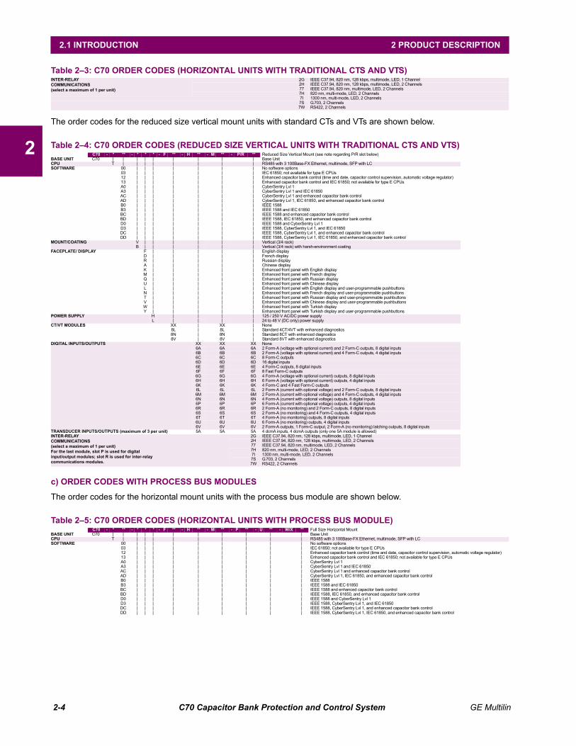
2-4 C70 Capacitor Bank Protection and Control System GE Multilin
2.1 INTRODUCTION 2 PRODUCT DESCRIPTION
2
The order codes for the reduced size vertical mount units with standard CTs and VTs are shown below.
c) ORDER CODES WITH PROCESS BUS MODULES
The order codes for the horizontal mount units with the process bus module are shown below.
INTER-RELAYCOMMUNICATIONS(select a maximum of 1 per unit)
2G IEEE C37.94, 820 nm, 128 kbps, multimode, LED, 1 Channel2H IEEE C37.94, 820 nm, 128 kbps, multimode, LED, 2 Channels77 IEEE C37.94, 820 nm, multimode, LED, 2 Channels7H 820 nm, multi-mode, LED, 2 Channels7I 1300 nm, multi-mode, LED, 2 Channels7S G.703, 2 Channels7W RS422, 2 Channels
Table 2–4: C70 ORDER CODES (REDUCED SIZE VERTICAL UNITS WITH TRADITIONAL CTS AND VTS)C70 - * ** - * * * - F ** - H ** - M ** - P/R ** Reduced Size Vertical Mount (see note regarding P/R slot below)
BASE UNIT C70 | | | | | | | | | Base UnitCPU T | | | | | | | | RS485 with 3 100Base-FX Ethernet, multimode, SFP with LCSOFTWARE 00 | | | | | | | No software options
03 | | | | | | | IEC 61850; not available for type E CPUs12 | | | | | | | Enhanced capacitor bank control (time and date, capacitor control supervision, automatic voltage regulator)13 | | | | | | | Enhanced capacitor bank control and IEC 61850; not available for type E CPUsA0 | | | | | | | CyberSentry Lvl 1A3 | | | | | | | CyberSentry Lvl 1 and IEC 61850AC | | | | | | | CyberSentry Lvl 1 and enhanced capacitor bank controlAD | | | | | | | CyberSentry Lvl 1, IEC 61850, and enhanced capacitor bank controlB0 | | | | | | | IEEE 1588B3 | | | | | | | IEEE 1588 and IEC 61850BC | | | | | | | IEEE 1588 and enhanced capacitor bank controlBD | | | | | | | IEEE 1588, IEC 61850, and enhanced capacitor bank controlD0 | | | | | | | IEEE 1588 and CyberSentry Lvl 1D3 | | | | | | | IEEE 1588, CyberSentry Lvl 1, and IEC 61850DC | | | | | | | IEEE 1588, CyberSentry Lvl 1, and enhanced capacitor bank controlDD | | | | | | | IEEE 1588, CyberSentry Lvl 1, IEC 61850, and enhanced capacitor bank control
MOUNT/COATING V | | | | | | Vertical (3/4 rack)B | | | | | | Vertical (3/4 rack) with harsh-environment coating
FACEPLATE/ DISPLAY F | | | | | English displayD | | | | | French displayR | | | | | Russian displayA | | | | | Chinese displayK | | | | | Enhanced front panel with English displayM | | | | | Enhanced front panel with French displayQ | | | | | Enhanced front panel with Russian displayU | | | | | Enhanced front panel with Chinese displayL | | | | | Enhanced front panel with English display and user-programmable pushbuttonsN | | | | | Enhanced front panel with French display and user-programmable pushbuttonsT | | | | | Enhanced front panel with Russian display and user-programmable pushbuttonsV | | | | | Enhanced front panel with Chinese display and user-programmable pushbuttonsW | | | | | Enhanced front panel with Turkish displayY | | | | | Enhanced front panel with Turkish display and user-programmable pushbuttons
POWER SUPPLY H | | | | 125 / 250 V AC/DC power supplyL | | | | 24 to 48 V (DC only) power supply
CT/VT MODULES XX | XX | None8L | 8L | Standard 4CT/4VT with enhanced diagnostics8N | 8N | Standard 8CT with enhanced diagnostics8V | 8V | Standard 8VT with enhanced diagnostics
DIGITAL INPUTS/OUTPUTS XX XX XX None6A 6A 6A 2 Form-A (voltage with optional current) and 2 Form-C outputs, 8 digital inputs6B 6B 6B 2 Form-A (voltage with optional current) and 4 Form-C outputs, 4 digital inputs6C 6C 6C 8 Form-C outputs6D 6D 6D 16 digital inputs6E 6E 6E 4 Form-C outputs, 8 digital inputs6F 6F 6F 8 Fast Form-C outputs6G 6G 6G 4 Form-A (voltage with optional current) outputs, 8 digital inputs6H 6H 6H 6 Form-A (voltage with optional current) outputs, 4 digital inputs6K 6K 6K 4 Form-C and 4 Fast Form-C outputs6L 6L 6L 2 Form-A (current with optional voltage) and 2 Form-C outputs, 8 digital inputs6M 6M 6M 2 Form-A (current with optional voltage) and 4 Form-C outputs, 4 digital inputs6N 6N 6N 4 Form-A (current with optional voltage) outputs, 8 digital inputs6P 6P 6P 6 Form-A (current with optional voltage) outputs, 4 digital inputs6R 6R 6R 2 Form-A (no monitoring) and 2 Form-C outputs, 8 digital inputs6S 6S 6S 2 Form-A (no monitoring) and 4 Form-C outputs, 4 digital inputs6T 6T 6T 4 Form-A (no monitoring) outputs, 8 digital inputs6U 6U 6U 6 Form-A (no monitoring) outputs, 4 digital inputs6V 6V 6V 2 Form-A outputs, 1 Form-C output, 2 Form-A (no monitoring) latching outputs, 8 digital inputs
TRANSDUCER INPUTS/OUTPUTS (maximum of 3 per unit) 5A 5A 5A 4 dcmA inputs, 4 dcmA outputs (only one 5A module is allowed)INTER-RELAYCOMMUNICATIONS(select a maximum of 1 per unit)For the last module, slot P is used for digital input/output modules; slot R is used for inter-relaycommunications modules.
2G IEEE C37.94, 820 nm, 128 kbps, multimode, LED, 1 Channel2H IEEE C37.94, 820 nm, 128 kbps, multimode, LED, 2 Channels77 IEEE C37.94, 820 nm, multimode, LED, 2 Channels7H 820 nm, multi-mode, LED, 2 Channels7I 1300 nm, multi-mode, LED, 2 Channels7S G.703, 2 Channels7W RS422, 2 Channels
Table 2–5: C70 ORDER CODES (HORIZONTAL UNITS WITH PROCESS BUS MODULE)C70 - * ** - * * * - F ** - H ** - M ** - P ** - U ** - W/X ** Full Size Horizontal Mount
BASE UNIT C70 | | | | | | | | | | | Base UnitCPU T | | | | | | | | | | RS485 with 3 100Base-FX Ethernet, multimode, SFP with LCSOFTWARE 00 | | | | | | | | | No software options
03 | | | | | | | | | IEC 61850; not available for type E CPUs12 | | | | | | | | | Enhanced capacitor bank control (time and date, capacitor control supervision, automatic voltage regulator)13 | | | | | | | | | Enhanced capacitor bank control and IEC 61850; not available for type E CPUsA0 | | | | | | | | | CyberSentry Lvl 1A3 | | | | | | | | | CyberSentry Lvl 1 and IEC 61850AC | | | | | | | | | CyberSentry Lvl 1 and enhanced capacitor bank controlAD | | | | | | | | | CyberSentry Lvl 1, IEC 61850, and enhanced capacitor bank controlB0 | | | | | | | | | IEEE 1588B3 | | | | | | | | | IEEE 1588 and IEC 61850BC | | | | | | | | | IEEE 1588 and enhanced capacitor bank controlBD | | | | | | | | | IEEE 1588, IEC 61850, and enhanced capacitor bank controlD0 | | | | | | | | | IEEE 1588 and CyberSentry Lvl 1D3 | | | | | | | | | IEEE 1588, CyberSentry Lvl 1, and IEC 61850DC | | | | | | | | | IEEE 1588, CyberSentry Lvl 1, and enhanced capacitor bank controlDD | | | | | | | | | IEEE 1588, CyberSentry Lvl 1, IEC 61850, and enhanced capacitor bank control
Table 2–3: C70 ORDER CODES (HORIZONTAL UNITS WITH TRADITIONAL CTS AND VTS)

GE Multilin C70 Capacitor Bank Protection and Control System 2-5
2 PRODUCT DESCRIPTION 2.1 INTRODUCTION
2
The order codes for the reduced size vertical mount units with the process bus module are shown below.
MOUNT/COATING H | | | | | | | | Horizontal (19” rack)A | | | | | | | | Horizontal (19” rack) with harsh environmental coating
FACEPLATE/ DISPLAY C | | | | | | | English displayP | | | | | | | English display with 4 small and 12 large programmable pushbuttonsD | | | | | | | French displayR | | | | | | | Russian displayA | | | | | | | Chinese displayK | | | | | | | Enhanced front panel with English displayM | | | | | | | Enhanced front panel with French displayQ | | | | | | | Enhanced front panel with Russian displayU | | | | | | | Enhanced front panel with Chinese displayL | | | | | | | Enhanced front panel with English display and user-programmable pushbuttonsN | | | | | | | Enhanced front panel with French display and user-programmable pushbuttonsT | | | | | | | Enhanced front panel with Russian display and user-programmable pushbuttonsV | | | | | | | Enhanced front panel with Chinese display and user-programmable pushbuttonsW | | | | | | | Enhanced front panel with Turkish display Y | | | | | | | Enhanced front panel with Turkish display and user-programmable pushbuttons
POWER SUPPLY H | | | | | | 125 / 250 V AC/DC power supplyL | | | | | | 24 to 48 V (DC only) power supply
PROCESS BUS MODULE XX | XX | | | None| 81 | | | | Standard 4CT/4VT with enhanced diagnostics
DIGITAL INPUTS/OUTPUTS XX XX XX None6A 6A | 2 Form-A (voltage with optional current) and 2 Form-C outputs, 8 digital inputs6B 6B | 2 Form-A (voltage with optional current) and 4 Form-C outputs, 4 digital inputs6C 6C | 8 Form-C outputs6D 6D | 16 digital inputs6E 6E | 4 Form-C outputs, 8 digital inputs6F 6F | 8 Fast Form-C outputs6G 6G | 4 Form-A (voltage with optional current) outputs, 8 digital inputs6H 6H | 6 Form-A (voltage with optional current) outputs, 4 digital inputs6K 6K | 4 Form-C and 4 Fast Form-C outputs6L 6L | 2 Form-A (current with optional voltage) and 2 Form-C outputs, 8 digital inputs6M 6M | 2 Form-A (current with optional voltage) and 4 Form-C outputs, 4 digital inputs6N 6N | 4 Form-A (current with optional voltage) outputs, 8 digital inputs6P 6P | 6 Form-A (current with optional voltage) outputs, 4 digital inputs6R 6R | 2 Form-A (no monitoring) and 2 Form-C outputs, 8 digital inputs6S 6S | 2 Form-A (no monitoring) and 4 Form-C outputs, 4 digital inputs6T 6T | 4 Form-A (no monitoring) outputs, 8 digital inputs6U 6U | 6 Form-A (no monitoring) outputs, 4 digital inputs6V 6V | 2 Form-A outputs, 1 Form-C output, 2 Form-A (no monitoring) latching outputs, 8 digital inputs
INTER-RELAYCOMMUNICATIONS(select a maximum of 1 per unit)
2G IEEE C37.94, 820 nm, 128 kbps, multimode, LED, 1 Channel2H IEEE C37.94, 820 nm, 128 kbps, multimode, LED, 2 Channels77 IEEE C37.94, 820 nm, multimode, LED, 2 Channels7H 820 nm, multi-mode, LED, 2 Channels7I 1300 nm, multi-mode, LED, 2 Channels7S G.703, 2 Channels7W RS422, 2 Channels
Table 2–6: C70 ORDER CODES (REDUCED SIZE VERTICAL UNITS WITH PROCESS BUS MODULE)C70 - * ** - * * * - F ** - H ** - M ** - P/R ** Reduced Size Vertical Mount (see note regarding P/R slot below)
BASE UNIT C70 | | | | | | | | | Base UnitCPU T | | | | | | | | RS485 with 3 100Base-FX Ethernet, multimode, SFP with LCSOFTWARE 00 | | | | | | | No software options
03 | | | | | | | IEC 61850; not available for type E CPUs12 | | | | | | | Enhanced capacitor bank control (time and date, capacitor control supervision, automatic voltage regulator)13 | | | | | | | Enhanced capacitor bank control and IEC 61850; not available for type E CPUsA0 | | | | | | | CyberSentry Lvl 1A3 | | | | | | | CyberSentry Lvl 1 and IEC 61850AC | | | | | | | CyberSentry Lvl 1 and enhanced capacitor bank controlAD | | | | | | | CyberSentry Lvl 1, IEC 61850, and enhanced capacitor bank controlB0 | | | | | | | IEEE 1588B3 | | | | | | | IEEE 1588 and IEC 61850BC | | | | | | | IEEE 1588 and enhanced capacitor bank controlBD | | | | | | | IEEE 1588, IEC 61850, and enhanced capacitor bank controlD0 | | | | | | | IEEE 1588 and CyberSentry Lvl 1D3 | | | | | | | IEEE 1588, CyberSentry Lvl 1, and IEC 61850DC | | | | | | | IEEE 1588, CyberSentry Lvl 1, and enhanced capacitor bank controlDD | | | | | | | IEEE 1588, CyberSentry Lvl 1, IEC 61850, and enhanced capacitor bank control
MOUNT/COATING V | | | | | | Vertical (3/4 rack)B | | | | | | Vertical (3/4 rack) with harsh environmental coating
FACEPLATE/ DISPLAY F | | | | | English displayD | | | | | French displayR | | | | | Russian displayA | | | | | Chinese displayK | | | | | Enhanced front panel with English displayM | | | | | Enhanced front panel with French displayQ | | | | | Enhanced front panel with Russian displayU | | | | | Enhanced front panel with Chinese displayL | | | | | Enhanced front panel with English display and user-programmable pushbuttonsN | | | | | Enhanced front panel with French display and user-programmable pushbuttonsT | | | | | Enhanced front panel with Russian display and user-programmable pushbuttonsV | | | | | Enhanced front panel with Chinese display and user-programmable pushbuttonsW | | | | | Enhanced front panel with Turkish display Y | | | | | Enhanced front panel with Turkish display and user-programmable pushbuttons
POWER SUPPLY H | | | | 125 / 250 V AC/DC power supplyL | | | | 24 to 48 V (DC only) power supply
PROCESS BUS MODULE XX | XX | None| 81 | | Standard 4CT/4VT with enhanced diagnostics
DIGITAL INPUTS/OUTPUTS XX None| 2 Form-A (voltage with optional current) and 2 Form-C outputs, 8 digital inputs| 2 Form-A (voltage with optional current) and 4 Form-C outputs, 4 digital inputs| 8 Form-C outputs| 16 digital inputs| 4 Form-C outputs, 8 digital inputs| 8 Fast Form-C outputs| 4 Form-A (voltage with optional current) outputs, 8 digital inputs| 6 Form-A (voltage with optional current) outputs, 4 digital inputs| 4 Form-C and 4 Fast Form-C outputs| 2 Form-A (current with optional voltage) and 2 Form-C outputs, 8 digital inputs| 2 Form-A (current with optional voltage) and 4 Form-C outputs, 4 digital inputs| 4 Form-A (current with optional voltage) outputs, 8 digital inputs| 6 Form-A (current with optional voltage) outputs, 4 digital inputs| 2 Form-A (no monitoring) and 2 Form-C outputs, 8 digital inputs| 2 Form-A (no monitoring) and 4 Form-C outputs, 4 digital inputs| 4 Form-A (no monitoring) outputs, 8 digital inputs| 6 Form-A (no monitoring) outputs, 4 digital inputs| 2 Form-A outputs, 1 Form-C output, 2 Form-A (no monitoring) latching outputs, 8 digital inputs
INTER-RELAYCOMMUNICATIONS(select a maximum of 1 per unit)For the last module, slot P is used for digital and transducerinput/output modules; slot R is used for inter-relaycommunications modules.
2G IEEE C37.94, 820 nm, 128 kbps, multimode, LED, 1 Channel2H IEEE C37.94, 820 nm, 128 kbps, multimode, LED, 2 Channels77 IEEE C37.94, 820 nm, multimode, LED, 2 Channels7H 820 nm, multi-mode, LED, 2 Channels7I 1300 nm, multi-mode, LED, 2 Channels7S G.703, 2 Channels7W RS422, 2 Channels
Table 2–5: C70 ORDER CODES (HORIZONTAL UNITS WITH PROCESS BUS MODULE)

2-6 C70 Capacitor Bank Protection and Control System GE Multilin
2.1 INTRODUCTION 2 PRODUCT DESCRIPTION
2
2.1.3 REPLACEMENT MODULES
Replacement modules can be ordered separately. When ordering a replacement CPU module or faceplate, provide theserial number of your existing unit.
Not all replacement modules may be applicable to the C70 relay. Only the modules specified in the order codes areavailable as replacement modules.
Replacement module codes are subject to change without notice. See the GE Multilin ordering page at http://www.gedigitalenergy.com/multilin/order.htm for the latest C70 ordering options.
The replacement module order codes for the horizontal mount units are shown below.
Table 2–7: ORDER CODES FOR REPLACEMENT MODULES, HORIZONTAL UNITSUR - ** - *
POWER SUPPLY (redundant supply only available in horizontal units; must be same type as main supply)
| RH H | Redundant 125 / 250 V AC/DC| RL H | Redundant 24 to 48 V (DC only)
CPU | T | RS485 with 3 100Base-FX Ethernet, multimode, SFP with LCFACEPLATE/DISPLAY | 3C | Horizontal faceplate with keypad and English display
| 3D | Horizontal faceplate with keypad and French display| 3R | Horizontal faceplate with keypad and Russian display| 3A | Horizontal faceplate with keypad and Chinese display| 3P | Horizontal faceplate with keypad, user-programmable pushbuttons, and English display| 3G | Horizontal faceplate with keypad, user-programmable pushbuttons, and French display| 3S | Horizontal faceplate with keypad, user-programmable pushbuttons, and Russian display| 3B | Horizontal faceplate with keypad, user-programmable pushbuttons, and Chinese display| 3K | Enhanced front panel with English display| 3M | Enhanced front panel with French display| 3Q | Enhanced front panel with Russian display| 3U | Enhanced front panel with Chinese display| 3L | Enhanced front panel with English display and user-programmable pushbuttons| 3N | Enhanced front panel with French display and user-programmable pushbuttons| 3T | Enhanced front panel with Russian display and user-programmable pushbuttons| 3V | Enhanced front panel with Chinese display and user-programmable pushbuttons
DIGITAL INPUTS AND OUTPUTS | 4A | 4 Solid-State (no monitoring) MOSFET outputs| 4B | 4 Solid-State (voltage with optional current) MOSFET outputs| 4C | 4 Solid-State (current with optional voltage) MOSFET outputs| 4D | 16 digital inputs with Auto-Burnishing| 4L | 14 Form-A (no monitoring) Latching outputs| 67 | 8 Form-A (no monitoring) outputs| 6A | 2 Form-A (voltage with optional current) and 2 Form-C outputs, 8 digital inputs| 6B | 2 Form-A (voltage with optional current) and 4 Form-C outputs, 4 digital inputs| 6C | 8 Form-C outputs| 6D | 16 digital inputs| 6E | 4 Form-C outputs, 8 digital inputs| 6F | 8 Fast Form-C outputs| 6G | 4 Form-A (voltage with optional current) outputs, 8 digital inputs| 6H | 6 Form-A (voltage with optional current) outputs, 4 digital inputs| 6K | 4 Form-C and 4 Fast Form-C outputs| 6L | 2 Form-A (current with optional voltage) and 2 Form-C outputs, 8 digital inputs| 6M | 2 Form-A (current with optional voltage) and 4 Form-C outputs, 4 digital inputs| 6N | 4 Form-A (current with optional voltage) outputs, 8 digital inputs| 6P | 6 Form-A (current with optional voltage) outputs, 4 digital inputs| 6R | 2 Form-A (no monitoring) and 2 Form-C outputs, 8 digital inputs| 6S | 2 Form-A (no monitoring) and 4 Form-C outputs, 4 digital inputs| 6T | 4 Form-A (no monitoring) outputs, 8 digital inputs| 6U | 6 Form-A (no monitoring) outputs, 4 digital inputs| 6V | 2 Form-A outputs, 1 Form-C output, 2 Form-A (no monitoring) latching outputs, 8 digital inputs
CT/VTMODULES(NOT AVAILABLE FOR THE C30)
| 8F | Standard 4CT/4VT| 8G | Sensitive Ground 4CT/4VT| 8H | Standard 8CT| 8J | Sensitive Ground 8CT| 8L | Standard 4CT/4VT with enhanced diagnostics| 8M | Sensitive Ground 4CT/4VT with enhanced diagnostics| 8N | Standard 8CT with enhanced diagnostics| 8R | Sensitive Ground 8CT with enhanced diagnostics
INTER-RELAY COMMUNICATIONS | 2A | C37.94SM, 1300nm single-mode, ELED, 1 channel single-mode| 2B | C37.94SM, 1300nm single-mode, ELED, 2 channel single-mode| 2E | Bi-phase, single channel| 2F | Bi-phase, dual channel| 2G | IEEE C37.94, 820 nm, 128 kbps, multimode, LED, 1 Channel| 2H | IEEE C37.94, 820 nm, 128 kbps, multimode, LED, 2 Channels| 72 | 1550 nm, single-mode, LASER, 1 Channel| 73 | 1550 nm, single-mode, LASER, 2 Channel| 74 | Channel 1 - RS422; Channel 2 - 1550 nm, single-mode, LASER| 75 | Channel 1 - G.703; Channel 2 - 1550 nm, Single-mode LASER| 76 | IEEE C37.94, 820 nm, multimode, LED, 1 Channel| 77 | IEEE C37.94, 820 nm, multimode, LED, 2 Channels| 7A | 820 nm, multi-mode, LED, 1 Channel| 7B | 1300 nm, multi-mode, LED, 1 Channel| 7C | 1300 nm, single-mode, ELED, 1 Channel| 7D | 1300 nm, single-mode, LASER, 1 Channel| 7E | Channel 1 - G.703; Channel 2 - 820 nm, multi-mode| 7F | Channel 1 - G.703; Channel 2 - 1300 nm, multi-mode| 7G | Channel 1 - G.703; Channel 2 - 1300 nm, single-mode ELED| 7H | 820 nm, multi-mode, LED, 2 Channels| 7I | 1300 nm, multi-mode, LED, 2 Channels| 7J | 1300 nm, single-mode, ELED, 2 Channels| 7K | 1300 nm, single-mode, LASER, 2 Channels| 7L | Channel 1 - RS422; Channel 2 - 820 nm, multi-mode, LED| 7M | Channel 1 - RS422; Channel 2 - 1300 nm, multi-mode, LED| 7N | Channel 1 - RS422; Channel 2 - 1300 nm, single-mode, ELED| 7P | Channel 1 - RS422; Channel 2 - 1300 nm, single-mode, LASER| 7Q | Channel 1 - G.703; Channel 2 - 1300 nm, single-mode LASER| 7R | G.703, 1 Channel| 7S | G.703, 2 Channels| 7T | RS422, 1 Channel| 7W | RS422, 2 Channels
TRANSDUCERINPUTS/OUTPUTS
| 5A | 4 dcmA inputs, 4 dcmA outputs (only one 5A module is allowed)| 5C | 8 RTD inputs| 5D | 4 RTD inputs, 4 dcmA outputs (only one 5D module is allowed)| 5E | 4 dcmA inputs, 4 RTD inputs| 5F | 8 dcmA inputs
NOTE
NOTE

GE Multilin C70 Capacitor Bank Protection and Control System 2-7
2 PRODUCT DESCRIPTION 2.1 INTRODUCTION
2
The replacement module order codes for the reduced-size vertical mount units are shown below.
Table 2–8: ORDER CODES FOR REPLACEMENT MODULES, VERTICAL UNITSUR - ** - *
POWER SUPPLY | RH V | 125 / 250 V AC/DC| RL V | 24 to 48 V (DC only)
CPU | T | RS485 with 3 100Base-FX Ethernet, multimode, SFP with LCFACEPLATE/DISPLAY | 3F | Vertical faceplate with keypad and English display
| 3D | Vertical faceplate with keypad and French display| 3R | Vertical faceplate with keypad and Russian display| 3K | Vertical faceplate with keypad and Chinese display| 3K | Enhanced front panel with English display| 3M | Enhanced front panel with French display| 3Q | Enhanced front panel with Russian display| 3U | Enhanced front panel with Chinese display| 3L | Enhanced front panel with English display and user-programmable pushbuttons| 3N | Enhanced front panel with French display and user-programmable pushbuttons| 3T | Enhanced front panel with Russian display and user-programmable pushbuttons| 3V | Enhanced front panel with Chinese display and user-programmable pushbuttons
DIGITALINPUTS/OUTPUTS
| 4A | 4 Solid-State (no monitoring) MOSFET outputs| 4B | 4 Solid-State (voltage with optional current) MOSFET outputs| 4C | 4 Solid-State (current with optional voltage) MOSFET outputs| 4D | 16 digital inputs with Auto-Burnishing| 4L | 14 Form-A (no monitoring) Latching outputs| 67 | 8 Form-A (no monitoring) outputs| 6A | 2 Form-A (voltage with optional current) and 2 Form-C outputs, 8 digital inputs| 6B | 2 Form-A (voltage with optional current) and 4 Form-C outputs, 4 digital inputs| 6C | 8 Form-C outputs| 6D | 16 digital inputs| 6E | 4 Form-C outputs, 8 digital inputs| 6F | 8 Fast Form-C outputs| 6G | 4 Form-A (voltage with optional current) outputs, 8 digital inputs| 6H | 6 Form-A (voltage with optional current) outputs, 4 digital inputs| 6K | 4 Form-C and 4 Fast Form-C outputs| 6L | 2 Form-A (current with optional voltage) and 2 Form-C outputs, 8 digital inputs| 6M | 2 Form-A (current with optional voltage) and 4 Form-C outputs, 4 digital inputs| 6N | 4 Form-A (current with optional voltage) outputs, 8 digital inputs| 6P | 6 Form-A (current with optional voltage) outputs, 4 digital inputs| 6R | 2 Form-A (no monitoring) and 2 Form-C outputs, 8 digital inputs| 6S | 2 Form-A (no monitoring) and 4 Form-C outputs, 4 digital inputs| 6T | 4 Form-A (no monitoring) outputs, 8 digital inputs| 6U | 6 Form-A (no monitoring) outputs, 4 digital inputs| 6V | 2 Form-A outputs, 1 Form-C output, 2 Form-A (no monitoring) latching outputs, 8 digital inputs
CT/VTMODULES(NOT AVAILABLE FOR THE C30)
| 8F | Standard 4CT/4VT| 8G | Sensitive Ground 4CT/4VT| 8H | Standard 8CT| 8L | Standard 4CT/4VT with enhanced diagnostics| 8N | Standard 8CT with enhanced diagnostics
INTER-RELAY COMMUNICATIONS | 2A | C37.94SM, 1300nm single-mode, ELED, 1 channel single-mode| 2B | C37.94SM, 1300nm single-mode, ELED, 2 channel single-mode| 2E | Bi-phase, single channel| 2F | Bi-phase, dual channel| 2G | IEEE C37.94, 820 nm, 128 kbps, multimode, LED, 1 Channel| 2H | IEEE C37.94, 820 nm, 128 kbps, multimode, LED, 2 Channels| 72 | 1550 nm, single-mode, LASER, 1 Channel| 73 | 1550 nm, single-mode, LASER, 2 Channel| 74 | Channel 1 - RS422; Channel 2 - 1550 nm, single-mode, LASER| 75 | Channel 1 - G.703; Channel 2 - 1550 nm, Single-mode LASER| 76 | IEEE C37.94, 820 nm, 64 kbps, multimode, LED, 1 Channel| 77 | IEEE C37.94, 820 nm, 64 kbps, multimode, LED, 2 Channels| 7A | 820 nm, multi-mode, LED, 1 Channel| 7B | 1300 nm, multi-mode, LED, 1 Channel| 7C | 1300 nm, single-mode, ELED, 1 Channel| 7D | 1300 nm, single-mode, LASER, 1 Channel| 7E | Channel 1 - G.703; Channel 2 - 820 nm, multi-mode| 7F | Channel 1 - G.703; Channel 2 - 1300 nm, multi-mode| 7G | Channel 1 - G.703; Channel 2 - 1300 nm, single-mode ELED| 7H | 820 nm, multi-mode, LED, 2 Channels| 7I | 1300 nm, multi-mode, LED, 2 Channels| 7J | 1300 nm, single-mode, ELED, 2 Channels| 7K | 1300 nm, single-mode, LASER, 2 Channels| 7L | Channel 1 - RS422; Channel 2 - 820 nm, multi-mode, LED| 7M | Channel 1 - RS422; Channel 2 - 1300 nm, multi-mode, LED| 7N | Channel 1 - RS422; Channel 2 - 1300 nm, single-mode, ELED| 7P | Channel 1 - RS422; Channel 2 - 1300 nm, single-mode, LASER| 7Q | Channel 1 - G.703; Channel 2 - 1300 nm, single-mode LASER| 7R | G.703, 1 Channel| 7S | G.703, 2 Channels| 7T | RS422, 1 Channel| 7W | RS422, 2 Channels
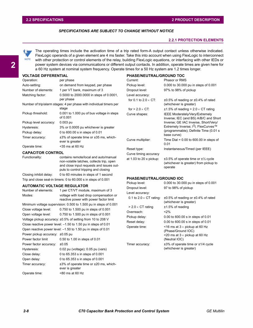
2-8 C70 Capacitor Bank Protection and Control System GE Multilin
2.2 SPECIFICATIONS 2 PRODUCT DESCRIPTION
2
2.2SPECIFICATIONSSPECIFICATIONS ARE SUBJECT TO CHANGE WITHOUT NOTICE
2.2.1 PROTECTION ELEMENTS
The operating times include the activation time of a trip rated form-A output contact unless otherwise indicated.FlexLogic operands of a given element are 4 ms faster. Take this into account when using FlexLogic to interconnectwith other protection or control elements of the relay, building FlexLogic equations, or interfacing with other IEDs orpower system devices via communications or different output contacts. In addition, operate times are given here fora 60 Hz system at nominal system frequency. Operate times for a 50 Hz system are 1.2 times longer.
VOLTAGE DIFFERENTIALOperation: per phase
Auto-setting: on demand from keypad, per phase
Number of elements: 1 per VT bank, maximum of 3
Matching factor: 0.5000 to 2000.0000 in steps of 0.0001, per phase
Number of trip/alarm stages: 4 per phase with individual timers per stage
Pickup threshold: 0.001 to 1.000 pu of bus voltage in steps of 0.001
Pickup level accuracy: 0.003 pu
Hysteresis: 3% or 0.0005 pu whichever is greater
Pickup delay: 0 to 600.00 s in steps of 0.01
Timer accuracy: ±3% of operate time or ±35 ms, which-ever is greater
Operate time: <35 ms at 60 Hz
CAPACITOR CONTROLFunctionality: contains remote/local and auto/manual
non-volatile latches, collects trip, open and close input requests and issues out-puts to control tripping and closing
Closing inhibit delay: 0 to 60 minutes in steps of 1 second
Trip and close seal-in timers: 0 to 60.000 s in steps of 0.001
AUTOMATIC VOLTAGE REGULATORNumber of elements: 1 per CT/VT module, maximum of 3
Modes: voltage with load drop compensation or reactive power with power factor limit
Minimum voltage supervision: 0.500 to 1.500 pu in steps of 0.001
Close voltage level: 0.750 to 1.500 pu in steps of 0.001
Open voltage level: 0.750 to 1.500 pu in steps of 0.001
Voltage pickup accuracy: ±0.5% of setting from 10 to 208 V
Close reactive power level: –1.50 to 1.50 pu in steps of 0.01
Open reactive power level: –1.50 to 1.50 pu in steps of 0.01
Power pickup accuracy: ±0.05 pu
Power factor limit 0.50 to 1.00 in steps of 0.01
Power factor accuracy: ±0.05
Hysteresis: 0.02 pu (voltage); 0.05 pu (vars)
Close delay: 0 to 65.353 s in steps of 0.001
Open delay: 0 to 65.353 s in steps of 0.001
Timer accuracy: ±3% of operate time or ±20 ms, which-ever is greater
Operate time: <80 ms at 60 Hz
PHASE/NEUTRAL/GROUND TOCCurrent: Phasor or RMS
Pickup level: 0.000 to 30.000 pu in steps of 0.001
Dropout level: 97% to 98% of pickup
Level accuracy:
for 0.1 to 2.0 CT: ±0.5% of reading or ±0.4% of rated(whichever is greater)
for > 2.0 CT: ±1.5% of reading > 2.0 CT rating
Curve shapes: IEEE Moderately/Very/Extremely Inverse; IEC (and BS) A/B/C and Short Inverse; GE IAC Inverse, Short/Very/ Extremely Inverse; I2t; FlexCurves™ (programmable); Definite Time (0.01 s base curve)
Curve multiplier: Time Dial = 0.00 to 600.00 in steps of 0.01
Reset type: Instantaneous/Timed (per IEEE)
Curve timing accuracy
at 1.03 to 20 x pickup: ±3.5% of operate time or ±½ cycle (whichever is greater) from pickup to operate
PHASE/NEUTRAL/GROUND IOCPickup level: 0.000 to 30.000 pu in steps of 0.001
Dropout level: 97 to 98% of pickup
Level accuracy:
0.1 to 2.0 CT rating: ±0.5% of reading or ±0.4% of rated(whichever is greater)
> 2.0 CT rating ±1.5% of reading
Overreach: <2%
Pickup delay: 0.00 to 600.00 s in steps of 0.01
Reset delay: 0.00 to 600.00 s in steps of 0.01
Operate time: <16 ms at 3 pickup at 60 Hz(Phase/Ground IOC)<20 ms at 3 pickup at 60 Hz(Neutral IOC)
Timer accuracy: ±3% of operate time or ±1/4 cycle (whichever is greater)
NOTE

GE Multilin C70 Capacitor Bank Protection and Control System 2-9
2 PRODUCT DESCRIPTION 2.2 SPECIFICATIONS
2
NEGATIVE SEQUENCE TOCPickup level: 0.000 to 30.000 pu in steps of 0.001
Dropout level: 97% to 98% of pickup
Level accuracy: ±0.5% of reading or ±0.4% of rated (whichever is greater)from 0.1 to 2.0 x CT rating±1.5% of reading > 2.0 x CT rating
Curve shapes: IEEE Moderately/Very/Extremely Inverse; IEC (and BS) A/B/C and Short Inverse; GE IAC Inverse, Short/Very/ Extremely Inverse; I2t; FlexCurves™ (programmable); Definite Time (0.01 s base curve)
Curve multiplier (Time dial): 0.00 to 600.00 in steps of 0.01
Reset type: Instantaneous/Timed (per IEEE) and Lin-ear
Curve timing accuracy
at 1.03 to 20 x pickup: ±3.5% of operate time or ±½ cycle (whichever is greater) from pickup to operate
NEGATIVE SEQUENCE IOCPickup level: 0.000 to 30.000 pu in steps of 0.001
Dropout level: 97 to 98% of pickup
Level accuracy: 0.1 to 2.0 CT rating: ±0.5% of reading or ±0.4% of rated (whichever is greater); 2.0 CT rating: ±1.5% of reading
Overreach: 2%
Pickup delay: 0.00 to 600.00 s in steps of 0.01
Reset delay: 0.00 to 600.00 s in steps of 0.01
Operate time: <20 ms at 3 pickup at 60 Hz
Timer accuracy: ±3% of operate time or ±1/4 cycle (whichever is greater)
PHASE DIRECTIONAL OVERCURRENTRelay connection: 90° (quadrature)
Quadrature voltage: ABC phase seq.: phase A (VBC), phase B (VCA), phase C (VAB); ACB phase seq.: phase A (VCB), phase B (VAC), phase C (VBA)
Polarizing voltage threshold: 0.000 to 3.000 pu in steps of 0.001
Current sensitivity threshold: 0.05 pu
Characteristic angle: 0 to 359° in steps of 1
Angle accuracy: ±2°
Operation time (FlexLogic operands):Tripping (reverse load, forward fault):
12 ms, typicallyBlocking (forward load, reverse fault):
8 ms, typically
NEUTRAL DIRECTIONAL OVERCURRENTDirectionality: Co-existing forward and reverse
Polarizing: Voltage, Current, Dual
Polarizing voltage: V_0 or VX
Polarizing current: IG
Operating current: I_0
Level sensing: 3 (|I_0| – K |I_1|), IGIndependent for forward and reverse
Restraint, K: 0.000 to 0.500 in steps of 0.001
Characteristic angle: –90 to 90° in steps of 1
Limit angle: 40 to 90° in steps of 1, independent for forward and reverse
Angle accuracy: ±2°
Offset impedance: 0.00 to 250.00 in steps of 0.01
Pickup level: 0.002 to 30.000 pu in steps of 0.01
Dropout level: 97 to 98%
Operation time: <16 ms at 3 pickup at 60 Hz
NEGATIVE SEQUENCE DIRECTIONAL OCDirectionality: Co-existing forward and reverse
Polarizing: Voltage
Polarizing voltage: V_2
Operating current: I_2
Level sensing:Zero-sequence:|I_0| – K |I_1|Negative-sequence:|I_2| – K |I_1|
Restraint, K: 0.000 to 0.500 in steps of 0.001
Characteristic angle: 0 to 90° in steps of 1
Limit angle: 40 to 90° in steps of 1, independent for forward and reverse
Angle accuracy: ±2°
Offset impedance: 0.00 to 250.00 in steps of 0.01
Pickup level: 0.015 to 30.000 pu in steps of 0.01
Dropout level: 97 to 98%
Operation time: <16 ms at 3 pickup at 60 Hz
PHASE CURRENT UNBALANCEOperation: per phase
Auto-setting: on demand from keypad, per phase
Number of elements: 1 per CT bank, maximum of 3
Inherent unbalance factor:–0.1000 to 0.1000 in steps of 0.0001, per phase
Number of trip/alarm stages: 4 per phase with individual timers per stage
Pickup threshold: 0.001 to 5.000 pu of split-phase CT nom-inal in steps of 0.001
Pickup level accuracy: 0.002 pu for <1 pu current and <20 CT mismatch between phase and differen-tial CT
Hysteresis: 3% or 0.001 pu, whichever is greater
Pickup delay: 0 to 600.00 s in steps of 0.01
Timer accuracy: ±3% of operate time or ±35 ms, which-ever is greater
Operate time: <35 ms at 60 Hz

2-10 C70 Capacitor Bank Protection and Control System GE Multilin
2.2 SPECIFICATIONS 2 PRODUCT DESCRIPTION
2
NEUTRAL CURRENT UNBALANCEAuto-setting: on demand from keypad
Number of elements: 1 per CT bank, to a maximum of 3
Inherent unbalance factor: magnitude of 0 to 0.1500 in steps of 0.0001, angle of 0 to 359° in steps of 1
Number of trip/alarm stages: 4, with individual timers per stage
Pickup threshold: 0.001 to 5.000 pu of ground input CT in steps of 0.001
Pickup level accuracy: 0.002 pu for <1 pu current and < 20 CT mismatch between phase and neutral CT
Hysteresis: 3% or 0.001 pu, whichever is greater
Slope: 0.0 to 10.0% in steps of 0.1
Pickup delay: 0 to 600.00 s in steps of 0.01
Timer accuracy: ±3% of operate time or ±35 ms, which-ever is greater
Operate time: <35 ms at 60 Hz
NEUTRAL VOLTAGE UNBALANCEOperation: compensated for inherent bank and sys-
tem unbalance
Auto-setting: on demand from keypad
Number of elements: 1 per VT bank, maximum of 3
Compensating factor: 0.7500 to 1.2500 in steps of 0.0001
Number of trip/alarm stages: 4 with individual timers
Pickup threshold: 0.001 to 1.000 pu of nominal of the bank neutral point VT in steps of 0.001
Slope: 0 to 10% in steps of 0.1
Pickup level accuracy: 0.003 pu for <10 VT mismatch between phase and neutral VT
Hysteresis: 3% or 0.001 pu whichever is greater
Pickup delay: 0 to 600.00 s in steps of 0.01
Timer accuracy: ±3% of operate time or ±35 ms, which-ever is greater
Operate time: <35 ms at 60 Hz
PHASE UNDERVOLTAGEPickup level: 0.000 to 3.000 pu in steps of 0.001
Dropout level: 102 to 103% of pickup
Level accuracy: ±0.5% of reading from 10 to 208 V
Curve shapes: GE IAV Inverse;Definite Time (0.1s base curve)
Curve multiplier: Time dial = 0.00 to 600.00 in steps of 0.01
Curve timing accuracy
at <0.90 x pickup: ±3.5% of operate time or ±1/2 cycle (whichever is greater) from pickup to operate
BANK OVERVOLTAGEOperation: per phase, 3 stages of definite-time, 1
stage of inverse-time
Application: grounded and ungrounded banks
Number of elements: 1 per VT bank, maximum of 3
Pickup threshold: 0.800 to 2.000 pu of bus voltage in steps of 0.001, per phase
Pickup level accuracy: 0.002 pu for operating voltage <70 V
Hysteresis: 0.02 pu
Pickup delay: 0 to 600.00 s in steps of 0.01
Curve: any user-programmable FlexCurve
Timer accuracy: ±3% of operate time or ±35 ms, which-ever is greater
Operate time: <35 ms at 60 Hz
PHASE OVERVOLTAGEVoltage: Phasor only
Pickup level: 0.000 to 3.000 pu in steps of 0.001
Dropout level: 97 to 98% of pickup
Level accuracy: ±0.5% of reading from 10 to 208 V
Pickup delay: 0.00 to 600.00 in steps of 0.01 s
Operate time: 30 ms at 1.10 pickup at 60 Hz
Timer accuracy: ±3% of operate time or ±1/4 cycle (whichever is greater)
NEUTRAL OVERVOLTAGEPickup level: 0.000 to 3.000 pu in steps of 0.001
Dropout level: 97 to 98% of pickup
Level accuracy: ±0.5% of reading from 10 to 208 V
Pickup delay: 0.00 to 600.00 s in steps of 0.01 (definite time) or user-defined curve
Reset delay: 0.00 to 600.00 s in steps of 0.01
Curve timing accuracy
at >1.1 x pickup: ±3.5% of operate time or ±1 cycle (whichever is greater) from pickup to operate
Operate time: 30 ms at 1.10 pickup at 60 Hz
AUXILIARY OVERVOLTAGEPickup level: 0.000 to 3.000 pu in steps of 0.001
Dropout level: 97 to 98% of pickup
Level accuracy: ±0.5% of reading from 10 to 208 V
Pickup delay: 0 to 600.00 s in steps of 0.01
Reset delay: 0 to 600.00 s in steps of 0.01
Timer accuracy: ±3% of operate time or ±1/4 cycle (whichever is greater)
Operate time: 30 ms at 1.10 pickup at 60 Hz
NEGATIVE SEQUENCE OVERVOLTAGEPickup level: 0.000 to 1.250 pu in steps of 0.001
Dropout level: 97 to 98% of pickup
Level accuracy: ±0.5% of reading from 10 to 208 V
Pickup delay: 0 to 600.00 s in steps of 0.01
Reset delay: 0 to 600.00 s in steps of 0.01
Timer accuracy: ±3% of operate time or ±20 ms, which-ever is greater
Operate time: <30 ms at 1.10 pickup at 60 Hz

GE Multilin C70 Capacitor Bank Protection and Control System 2-11
2 PRODUCT DESCRIPTION 2.2 SPECIFICATIONS
2
BREAKER FAILUREMode: 1-pole, 3-pole
Current supervision: phase, neutral current
Current supv. pickup: 0.001 to 30.000 pu in steps of 0.001
Current supv. dropout: 97 to 98% of pickup
Current supv. accuracy:
0.1 to 2.0 CT rating: ±0.75% of reading or ±2% of rated(whichever is greater)
above 2 CT rating: ±2.5% of reading
BREAKER FLASHOVEROperating quantity: phase current, voltage and voltage differ-
ence
Pickup level voltage: 0 to 1.500 pu in steps of 0.001
Dropout level voltage: 97 to 98% of pickup
Pickup level current: 0 to 1.500 pu in steps of 0.001
Dropout level current: 97 to 98% of pickup
Level accuracy: ±0.5% or ±0.1% of rated, whichever is greater
Pickup delay: 0 to 65.535 s in steps of 0.001
Timer accuracy: ±3% of operate time or ±42 ms, which-ever is greater
Operate time: <42 ms at 1.10 pickup at 60 Hz
BREAKER RESTRIKEPrinciple: detection of high-frequency overcurrent
condition ¼ cycle after breaker opens
Availability: one per CT/VT module (not including 8Z modules)
Pickup level: 0.1 to 2.00 pu in steps of 0.01
Reset delay: 0.000 to 65.535 s in steps of 0.001
THERMAL OVERLOAD PROTECTIONThermal overload curves: IEC 255-8 curve
Base current: 0.20 to 3.00 pu in steps of 0.01
Overload (k) factor: 1.00 to 1.20 pu in steps of 0.05
Trip time constant: 0 to 1000 min. in steps of 1
Reset time constant: 0 to 1000 min. in steps of 1
Minimum reset time: 0 to 1000 min. in steps of 1
Timer accuracy (cold curve): ±100 ms or 2%, whichever is greater
Timer accuracy (hot curve): ±500 ms or 2%, whichever is greater for Ip < 0.9 × k × Ib and I / (k × Ib) > 1.1
TRIP BUS (TRIP WITHOUT FLEXLOGIC)Number of elements: 6
Number of inputs: 16
Operate time: <2 ms at 60 Hz
Timer accuracy: ±3% or 10 ms, whichever is greater
2.2.2 USER-PROGRAMMABLE ELEMENTS
FLEXLOGICProgramming language: Reverse Polish Notation with graphical
visualization (keypad programmable)
Lines of code: 512
Internal variables: 64
Supported operations: NOT, XOR, OR (2 to 16 inputs), AND (2 to 16 inputs), NOR (2 to 16 inputs), NAND (2 to 16 inputs), latch (reset-domi-nant), edge detectors, timers
Inputs: any logical variable, contact, or virtual input
Number of timers: 32
Pickup delay: 0 to 60000 (ms, sec., min.) in steps of 1
Dropout delay: 0 to 60000 (ms, sec., min.) in steps of 1
FLEXCURVES™Number: 4 (A through D)
Reset points: 40 (0 through 1 of pickup)
Operate points: 80 (1 through 20 of pickup)
Time delay: 0 to 65535 ms in steps of 1
FLEX STATESNumber: up to 256 logical variables grouped
under 16 Modbus addresses
Programmability: any logical variable, contact, or virtual input
FLEXELEMENTS™Number of elements: 16
Operating signal: any analog actual value, or two values in differential mode
Operating signal mode: signed or absolute value
Operating mode: level, delta
Comparator direction: over, under
Pickup Level: –90.000 to 90.000 pu in steps of 0.001
Hysteresis: 0.1 to 50.0% in steps of 0.1
Delta dt: 20 ms to 60 days
Pickup & dropout delay: 0.000 to 65.535 s in steps of 0.001
NON-VOLATILE LATCHESType: set-dominant or reset-dominant
Number: 16 (individually programmed)
Output: stored in non-volatile memory
Execution sequence: as input prior to protection, control, and FlexLogic
USER-PROGRAMMABLE LEDsNumber: 48 plus trip and alarm
Programmability: from any logical variable, contact, or vir-tual input
Reset mode: self-reset or latched

2-12 C70 Capacitor Bank Protection and Control System GE Multilin
2.2 SPECIFICATIONS 2 PRODUCT DESCRIPTION
2
LED TESTInitiation: from any digital input or user-program-
mable condition
Number of tests: 3, interruptible at any time
Duration of full test: approximately 3 minutes
Test sequence 1: all LEDs on
Test sequence 2: all LEDs off, one LED at a time on for 1 s
Test sequence 3: all LEDs on, one LED at a time off for 1 s
USER-DEFINABLE DISPLAYSNumber of displays: 16
Lines of display: 2 20 alphanumeric characters
Parameters: up to 5, any Modbus register addresses
Invoking and scrolling: keypad, or any user-programmable con-dition, including pushbuttons
CONTROL PUSHBUTTONSNumber of pushbuttons: 7
Operation: drive FlexLogic operands
USER-PROGRAMMABLE PUSHBUTTONS (OPTIONAL)Number of pushbuttons: 12 (standard faceplate);
16 (enhanced faceplate)
Mode: self-reset, latched
Display message: 2 lines of 20 characters each
Drop-out timer: 0.00 to 60.00 s in steps of 0.05
Autoreset timer: 0.2 to 600.0 s in steps of 0.1
Hold timer: 0.0 to 10.0 s in steps of 0.1
SELECTOR SWITCHNumber of elements: 2
Upper position limit: 1 to 7 in steps of 1
Selecting mode: time-out or acknowledge
Time-out timer: 3.0 to 60.0 s in steps of 0.1
Control inputs: step-up and 3-bit
Power-up mode: restore from non-volatile memory or syn-chronize to a 3-bit control input or synch/restore mode
TIME OF DAY TIMERSNumber of timers: 5
Setting resolution: 1 minute
DIGITAL ELEMENTSNumber of elements: 48
Operating signal: any FlexLogic operand
Pickup delay: 0.000 to 999999.999 s in steps of 0.001
Dropout delay: 0.000 to 999999.999 s in steps of 0.001
Timing accuracy: ±3% or ±4 ms, whichever is greater
2.2.3 MONITORING
OSCILLOGRAPHYMaximum records: 64
Sampling rate: 64 samples per power cycle
Triggers: any element pickup, dropout, or operate; digital input change of state; digital out-put change of state; FlexLogic equation
Data: AC input channels; element state; digital input state; digital output state
Data storage: in non-volatile memory
EVENT RECORDERCapacity: 1024 events
Time-tag: to 1 microsecond
Triggers: any element pickup, dropout, or operate; digital input change of state; digital out-put change of state; self-test events
Data storage: in non-volatile memory
USER-PROGRAMMABLE FAULT REPORTNumber of elements: 2
Pre-fault trigger: any FlexLogic operand
Fault trigger: any FlexLogic operand
Recorder quantities: 32 (any FlexAnalogTM value)
DATA LOGGERNumber of channels: 1 to 16
Parameters: any available analog actual value
Sampling rate: 15 to 3600000 ms in steps of 1
Trigger: any FlexLogic operand
Mode: continuous or triggered
Storage capacity: (NN is dependent on memory)
1-second rate:01 channel for NN days
16 channels for NN days
60-minute rate:
01 channel for NN days16 channels for NN days
2.2.4 METERING
RMS CURRENT: PHASE, NEUTRAL, AND GROUNDAccuracy at
0.1 to 2.0 CT rating: ±0.25% of reading or ±0.1% of rated(whichever is greater)
2.0 CT rating: ±1.0% of reading
RMS VOLTAGEAccuracy: ±0.5% of reading from 10 to 208 V

GE Multilin C70 Capacitor Bank Protection and Control System 2-13
2 PRODUCT DESCRIPTION 2.2 SPECIFICATIONS
2
REAL POWER (WATTS)Accuracy at 0.1 to 1.5 x
CT rating and 0.8 to
1.2 x VT rating: ±1.0% of reading at –1.0 PF< –0.8
REACTIVE POWER (VARS)Accuracy at 0.1 to 1.5 x
CT rating and 0.8 to
1.2 x VT rating: ±1.0% of reading at –0.2 PF 0.2
APPARENT POWER (VA)Accuracy at 0.1 to 1.5 x
CT rating and 0.8 to
1.2 x VT rating: ±1.0% of reading
CURRENT HARMONICSHarmonics: 2nd to 25th harmonic: per phase, dis-
played as a % of f1 (fundamental fre-quency phasor)THD: per phase, displayed as a % of f1
Accuracy:HARMONICS: 1. f1 > 0.4pu: (0.20% + 0.035% / harmonic) of
reading or 0.15% of 100%, whichever is greater2. f1 < 0.4pu: as above plus %error of f1
THD: 1. f1 > 0.4pu: (0.25% + 0.035% / harmonic) of reading or 0.20% of 100%, whichever is greater2. f1 < 0.4pu: as above plus %error of f1
VOLTAGE HARMONICSHarmonics: 2nd to 25th harmonic: per phase, dis-
played as a % of f1 (fundamental fre-quency phasor)THD: per phase, displayed as a % of f1
Accuracy:HARMONICS: 1. f1 > 0.4pu: (0.20% + 0.035% / harmonic) of
reading or 0.15% of 100%, whichever is greater2. f1 < 0.4pu: as above plus %error of f1
THD: 1. f1 > 0.4pu: (0.25% + 0.035% / harmonic) of reading or 0.20% of 100%, whichever is greater2. f1 < 0.4pu: as above plus %error of f1
FREQUENCYAccuracy at
V = 0.8 to 1.2 pu: ±0.001 Hz (when voltage signal is used for frequency measurement)
I = 0.1 to 0.25 pu: ±0.05 HzI > 0.25 pu: ±0.001 Hz (when current signal is used
for frequency measurement)
2.2.5 INPUTS
AC CURRENTCT rated primary: 1 to 50000 A
CT rated secondary: 1 A or 5 A by connection
Relay burden: < 0.2 VA at rated secondary
Conversion range:Standard CT: 0.02 to 46 CT rating RMS symmetrical
Current withstand: 20 ms at 250 times rated1 sec. at 100 times ratedcontinuous 4xInom; URs equipped with 24 CT inputs have a maximum operating temp. of 50°C
Short circuit rating: 150000 RMS symmetrical amperes, 250 V maximum (primary current to external CT)
AC VOLTAGEVT rated secondary: 50.0 to 240.0 V
VT ratio: 1.00 to 24000.00Relay burden:< 0.25 VA at 120 V
Conversion range: 1 to 275 V
Voltage withstand: continuous at 260 V to neutral1 min./hr at 420 V to neutral
FREQUENCYNominal frequency setting:25 to 60 Hz
Sampling frequency: 64 samples per power cycle
Tracking frequency range:20 to 70 Hz
CONTACT INPUTSDry contacts: 1000 maximum
Wet contacts: 300 V DC maximum
Selectable thresholds: 17 V, 33 V, 84 V, 166 V
Tolerance: ±10%
Contacts per common return: 4
Recognition time: < 1 ms
Debounce time: 0.0 to 16.0 ms in steps of 0.5
Continuous current draw:3 mA (when energized)
CONTACT INPUTS WITH AUTO-BURNISHINGDry contacts: 1000 maximum
Wet contacts: 300 V DC maximum
Selectable thresholds: 17 V, 33 V, 84 V, 166 V
Tolerance: ±10%
Contacts per common return: 2
Recognition time: < 1 ms
Debounce time: 0.0 to 16.0 ms in steps of 0.5
Continuous current draw:3 mA (when energized)
Auto-burnish impulse current: 50 to 70 mA
Duration of auto-burnish impulse: 25 to 50 ms

2-14 C70 Capacitor Bank Protection and Control System GE Multilin
2.2 SPECIFICATIONS 2 PRODUCT DESCRIPTION
2
DCMA INPUTSCurrent input (mA DC): 0 to –1, 0 to +1, –1 to +1, 0 to 5, 0 to 10,
0 to 20, 4 to 20 (programmable)
Input impedance: 379 ±10%
Conversion range: –1 to + 20 mA DC
Accuracy: ±0.2% of full scale
Type: Passive
IRIG-B INPUTAmplitude modulation: 1 to 10 V pk-pk
DC shift: TTL–Compatible
Input impedance: 50 kIsolation: 2 kV
REMOTE INPUTS (IEC 61850 GSSE/GOOSE)Input points: 32, configured from 64 incoming bit pairs
Remote devices: 16
Default states on loss of comms.: On, Off, Latest/Off, Latest/On
Remote DPS inputs: 5
DIRECT INPUTSInput points: 32
Remote devices: 16
Default states on loss of comms.: On, Off, Latest/Off, Latest/On
Ring configuration: Yes, No
Data rate: 64 or 128 kbps
CRC: 32-bit
CRC alarm:Responding to: Rate of messages failing the CRCMonitoring message count: 10 to 10000 in steps of 1Alarm threshold: 1 to 1000 in steps of 1
Unreturned message alarm:Responding to: Rate of unreturned messages in the ring
configurationMonitoring message count: 10 to 10000 in steps of 1Alarm threshold: 1 to 1000 in steps of 1
2.2.6 POWER SUPPLY
LOW RANGENominal DC voltage: 24 to 48 V
Minimum DC voltage: 20 V
Maximum DC voltage: 60 V
Voltage loss hold-up: 20 ms duration at nominal
NOTE: Low range is DC only.
HIGH RANGENominal DC voltage: 125 to 250 V
Minimum DC voltage: 88 V
Maximum DC voltage: 300 V
Nominal AC voltage: 100 to 240 V at 50/60 Hz
Minimum AC voltage: 88 V at 25 to 100 Hz
Maximum AC voltage: 265 V at 25 to 100 Hz
Voltage loss hold-up: 200 ms duration at nominal
ALL RANGESVolt withstand: 2 Highest Nominal Voltage for 10 ms
Power consumption: typical = 15 to 20 W/VAmaximum = 50 W/VAcontact factory for exact order code con-sumption
INTERNAL FUSERATINGS
Low range power supply: 8 A / 250 VHigh range power supply: 4 A / 250 V
INTERRUPTING CAPACITYAC: 100 000 A RMS symmetricalDC: 10 000 A
2.2.7 OUTPUTS
FORM-A RELAY
Make and carry for 0.2 s: 30 A as per ANSI C37.90
Carry continuous: 6 A
Break (DC inductive, L/R = 40 ms):
Operate time: < 4 ms
Contact material: silver alloy
LATCHING RELAYMake and carry for 0.2 s: 30 A as per ANSI C37.90
Carry continuous: 6 A as per IEEE C37.90
Break (DC resistive as per IEC61810-1):
Operate time: < 4 ms
Contact material: silver alloy
Control: separate operate and reset inputs
Control mode: operate-dominant or reset-dominant
FORM-A VOLTAGE MONITORApplicable voltage: approx. 15 to 250 V DC
Trickle current: approx. 1 to 2.5 mA
VOLTAGE CURRENT
24 V 1 A
48 V 0.5 A
125 V 0.3 A
250 V 0.2 A
VOLTAGE CURRENT
24 V 6 A
48 V 1.6 A
125 V 0.4 A
250 V 0.2 A

GE Multilin C70 Capacitor Bank Protection and Control System 2-15
2 PRODUCT DESCRIPTION 2.2 SPECIFICATIONS
2
FORM-A CURRENT MONITORThreshold current: approx. 80 to 100 mA
FORM-C AND CRITICAL FAILURE RELAYMake and carry for 0.2 s: 30 A as per ANSI C37.90
Carry continuous: 8 A
Break (DC inductive, L/R = 40 ms):
Operate time: < 8 ms
Contact material: silver alloy
FAST FORM-C RELAYMake and carry: 0.1 A max. (resistive load)
Minimum load impedance:
Operate time: < 0.6 ms
Internal Limiting Resistor: 100 , 2 W
SOLID-STATE OUTPUT RELAYOperate and release time: <100 s
Maximum voltage: 265 V DC
Maximum continuous current: 5 A at 45°C; 4 A at 65°C
Make and carry:for 0.2 s: 30 A as per ANSI C37.90for 0.03 s 300 A
Breaking capacity:
CONTROL POWER EXTERNAL OUTPUT(FOR DRY CONTACT INPUT)Capacity: 100 mA DC at 48 V DC
Isolation: ±300 Vpk
REMOTE OUTPUTS (IEC 61850 GSSE/GOOSE)Standard output points: 32
User output points: 32
DIRECT OUTPUTSOutput points: 32
DCMA OUTPUTSRange: –1 to 1 mA, 0 to 1 mA, 4 to 20 mA
Max. load resistance: 12 k for –1 to 1 mA range12 k for 0 to 1 mA range600 for 4 to 20 mA range
Accuracy: ±0.75% of full-scale for 0 to 1 mA range±0.5% of full-scale for –1 to 1 mA range±0.75% of full-scale for 0 to 20 mA range
99% Settling time to a step change: 100 ms
Isolation: 1.5 kV
Driving signal: any FlexAnalog quantity
Upper and lower limit for the driving signal: –90 to 90 pu in steps of 0.001
VOLTAGE CURRENT
24 V 1 A
48 V 0.5 A
125 V 0.3 A
250 V 0.2 A
INPUTVOLTAGE
IMPEDANCE
2 W RESISTOR 1 W RESISTOR
250 V DC 20 K 50 K
120 V DC 5 K 2 K
48 V DC 2 K 2 K
24 V DC 2 K 2 K
Note: values for 24 V and 48 V are the same due to a required 95% voltage drop across the load impedance.
UL508 Utility application
(autoreclose scheme)
Industrial application
Operations/interval
5000 ops /1 s-On, 9 s-Off
5 ops /0.2 s-On, 0.2 s-Offwithin 1 minute
10000 ops /0.2 s-On, 30 s-Off 1000 ops /
0.5 s-On, 0.5 s-Off
Break capability(0 to 250 V DC)
3.2 AL/R = 10 ms
10 AL/R = 40 ms
10 AL/R = 40 ms
1.6 AL/R = 20 ms
0.8 AL/R = 40 ms
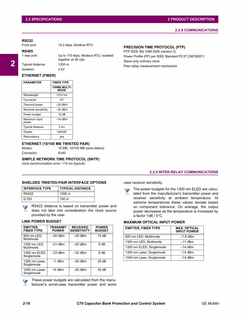
2-16 C70 Capacitor Bank Protection and Control System GE Multilin
2.2 SPECIFICATIONS 2 PRODUCT DESCRIPTION
2
2.2.8 COMMUNICATIONS
RS232Front port: 19.2 kbps, Modbus RTU
RS4851 rear port: Up to 115 kbps, Modbus RTU, isolated
together at 36 Vpk
Typical distance: 1200 m
Isolation: 2 kV
ETHERNET (FIBER)
ETHERNET (10/100 MB TWISTED PAIR)Modes: 10 MB, 10/100 MB (auto-detect)
Connector: RJ45
SIMPLE NETWORK TIME PROTOCOL (SNTP)clock synchronization error: <10 ms (typical)
PRECISION TIME PROTOCOL (PTP)PTP IEEE Std 1588 2008 (version 2)
Power Profile (PP) per IEEE Standard PC37.238TM2011
Slave-only ordinary clock
Peer delay measurement mechanism
2.2.9 INTER-RELAY COMMUNICATIONS
SHIELDED TWISTED-PAIR INTERFACE OPTIONS
RS422 distance is based on transmitter power anddoes not take into consideration the clock sourceprovided by the user.
LINK POWER BUDGET
These power budgets are calculated from the manu-facturer’s worst-case transmitter power and worst
case receiver sensitivity.
The power budgets for the 1300 nm ELED are calcu-lated from the manufacturer's transmitter power andreceiver sensitivity at ambient temperature. Atextreme temperatures these values deviate basedon component tolerance. On average, the outputpower decreases as the temperature is increased bya factor 1dB / 5°C.
MAXIMUM OPTICAL INPUT POWER
PARAMETER FIBER TYPE
100MB MULTI-MODE
Wavelength 1310 nm
Connector ST
Transmit power –20 dBm
Receiver sensitivity –30 dBm
Power budget 10 dB
Maximum input power
–14 dBm
Typical distance 2 km
Duplex full/half
Redundancy yes
INTERFACE TYPE TYPICAL DISTANCE
RS422 1200 m
G.703 100 m
EMITTER, FIBER TYPE
TRANSMIT POWER
RECEIVED SENSITIVITY
POWER BUDGET
820 nm LED,Multimode
–20 dBm –30 dBm 10 dB
1300 nm LED,Multimode
–21 dBm –30 dBm 9 dB
1300 nm ELED, Singlemode
–23 dBm –32 dBm 9 dB
1300 nm Laser, Singlemode
–1 dBm –30 dBm 29 dB
1550 nm Laser, Singlemode
+5 dBm –30 dBm 35 dB
NOTE
NOTE
EMITTER, FIBER TYPE MAX. OPTICALINPUT POWER
820 nm LED, Multimode –7.6 dBm
1300 nm LED, Multimode –11 dBm
1300 nm ELED, Singlemode –14 dBm
1300 nm Laser, Singlemode –14 dBm
1550 nm Laser, Singlemode –14 dBm
NOTE
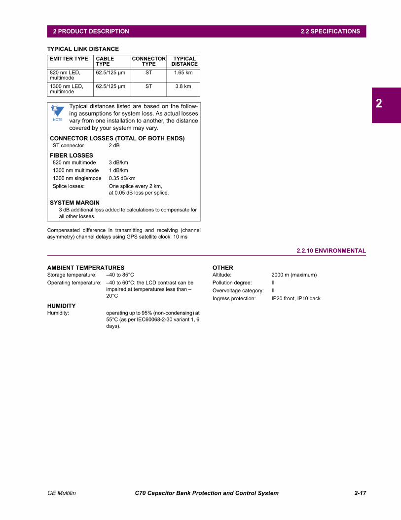
GE Multilin C70 Capacitor Bank Protection and Control System 2-17
2 PRODUCT DESCRIPTION 2.2 SPECIFICATIONS
2
TYPICAL LINK DISTANCE
Compensated difference in transmitting and receiving (channelasymmetry) channel delays using GPS satellite clock: 10 ms
2.2.10 ENVIRONMENTAL
AMBIENT TEMPERATURESStorage temperature: –40 to 85°C
Operating temperature: –40 to 60°C; the LCD contrast can be impaired at temperatures less than –20°C
HUMIDITYHumidity: operating up to 95% (non-condensing) at
55°C (as per IEC60068-2-30 variant 1, 6 days).
OTHERAltitude: 2000 m (maximum)
Pollution degree: II
Overvoltage category: II
Ingress protection: IP20 front, IP10 back
EMITTER TYPE CABLE TYPE
CONNECTOR TYPE
TYPICALDISTANCE
820 nm LED,multimode
62.5/125 μm ST 1.65 km
1300 nm LED,multimode
62.5/125 μm ST 3.8 km
Typical distances listed are based on the follow-ing assumptions for system loss. As actual lossesvary from one installation to another, the distancecovered by your system may vary.
CONNECTOR LOSSES (TOTAL OF BOTH ENDS)ST connector 2 dB
FIBER LOSSES820 nm multimode 3 dB/km
1300 nm multimode 1 dB/km
1300 nm singlemode 0.35 dB/km
Splice losses: One splice every 2 km,at 0.05 dB loss per splice.
SYSTEM MARGIN3 dB additional loss added to calculations to compensate for all other losses.
NOTE

2-18 C70 Capacitor Bank Protection and Control System GE Multilin
2.2 SPECIFICATIONS 2 PRODUCT DESCRIPTION
2
2.2.11 TYPE TESTS
C70 TYPE TESTS
2.2.12 PRODUCTION TESTS
THERMALProducts go through an environmental test based upon an
Accepted Quality Level (AQL) sampling process.
TEST REFERENCE STANDARD TEST LEVEL
Dielectric voltage withstand EN60255-5 2.2 kV
Impulse voltage withstand EN60255-5 5 kV
Damped oscillatory IEC61000-4-18 / IEC60255-22-1 2.5 kV CM, 1 kV DM
Electrostatic discharge EN61000-4-2 / IEC60255-22-2 Level 3
RF immunity EN61000-4-3 / IEC60255-22-3 Level 3
Fast transient disturbance EN61000-4-4 / IEC60255-22-4 Class A and B
Surge immunity EN61000-4-5 / IEC60255-22-5 Level 3 and 4
Conducted RF immunity EN61000-4-6 / IEC60255-22-6 Level 3
Power frequency immunity EN61000-4-7 / IEC60255-22-7 Class A and B
Voltage interruption and ripple DC IEC60255-11 12% ripple, 200 ms interrupts
Radiated and conducted emissions CISPR11 / CISPR22 / IEC60255-25 Class A
Sinusoidal vibration IEC60255-21-1 Class 1
Shock and bump IEC60255-21-2 Class 1
Seismic IEC60255-21-3 Class 1
Power magnetic immunity IEC61000-4-8 Level 5
Pulse magnetic immunity IEC61000-4-9 Level 4
Damped magnetic immunity IEC61000-4-10 Level 4
Voltage dip and interruption IEC61000-4-11 0, 40, 70, 80% dips; 250 / 300 cycle interrupts
Damped oscillatory IEC61000-4-12 2.5 kV CM, 1 kV DM
Conducted RF immunity, 0 to 150 kHz IEC61000-4-16 Level 4
Voltage ripple IEC61000-4-17 15% ripple
Ingress protection IEC60529 IP40 front, IP10 back
Cold IEC60068-2-1 –40°C for 16 hours
Hot IEC60068-2-2 85°C for 16 hours
Humidity IEC60068-2-30 6 days, variant 1
Damped oscillatory IEEE/ANSI C37.90.1 2.5 kV, 1 MHz
RF immunity IEEE/ANSI C37.90.2 20 V/m, 80 MHz to 1 GHz
Safety UL508 e83849 NKCR
Safety UL C22.2-14 e83849 NKCR7
Safety UL1053 e83849 NKCR

GE Multilin C70 Capacitor Bank Protection and Control System 2-19
2 PRODUCT DESCRIPTION 2.2 SPECIFICATIONS
2
2.2.13 APPROVALS
APPROVALS
2.2.14 MAINTENANCE
MOUNTINGAttach mounting brackets using 20 inch-pounds (±2 inch-pounds) of torque.
CLEANINGNormally, cleaning is not required; but for situations where dust has accumulated on the faceplate display, a dry cloth can be used.
To avoid deterioration of electrolytic capacitors, power up units that are stored in a de-energized state once per year, for one hour continuously.
COMPLIANCE APPLICABLE COUNCIL DIRECTIVE
ACCORDING TO
CE Low voltage directive EN 60255-5
EMC directive EN 60255-26 / EN 50263
EN 61000-6-5
C-UL-US --- UL 508
UL 1053
C22.2 No. 14

2-20 C70 Capacitor Bank Protection and Control System GE Multilin
2.2 SPECIFICATIONS 2 PRODUCT DESCRIPTION
2

GE Multilin C70 Capacitor Bank Protection and Control System 3-1
3 HARDWARE 3.1 DESCRIPTION
3
3 HARDWARE 3.1DESCRIPTION 3.1.1 PANEL CUTOUT
a) HORIZONTAL UNITS
The C70 Capacitor Bank Protection and Control System is available as a 19-inch rack horizontal mount unit with a remov-able faceplate. The faceplate can be specified as either standard or enhanced at the time of ordering. The enhanced face-plate contains additional user-programmable pushbuttons and LED indicators.
The modular design allows the relay to be easily upgraded or repaired by a qualified service person. The faceplate ishinged to allow easy access to the removable modules, and is itself removable to allow mounting on doors with limited reardepth.
The case dimensions are shown below, along with panel cutout details for panel mounting. When planning the location ofyour panel cutout, ensure that provision is made for the faceplate to swing open without interference to or from adjacentequipment.
The relay must be mounted such that the faceplate sits semi-flush with the panel or switchgear door, allowing the operatoraccess to the keypad and the RS232 communications port. The relay is secured to the panel with the use of four screwssupplied with the relay.
Figure 3–1: C70 HORIZONTAL DIMENSIONS (ENHANCED PANEL)
17.56”
[446,02 mm]
9.687”
[246,05 mm]
11.016”
[279,81 mm]
7.460”
[189,48 mm]
6.960”
[176,78 mm]
19.040”
[483,62 mm]
6.995”
[177,67 mm]
842807A1.CDR
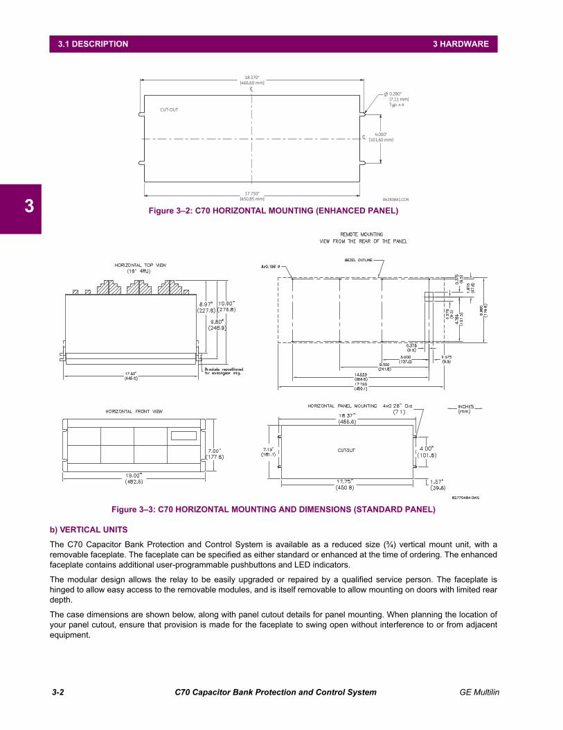
3-2 C70 Capacitor Bank Protection and Control System GE Multilin
3.1 DESCRIPTION 3 HARDWARE
3 Figure 3–2: C70 HORIZONTAL MOUNTING (ENHANCED PANEL)
Figure 3–3: C70 HORIZONTAL MOUNTING AND DIMENSIONS (STANDARD PANEL)
b) VERTICAL UNITS
The C70 Capacitor Bank Protection and Control System is available as a reduced size (¾) vertical mount unit, with aremovable faceplate. The faceplate can be specified as either standard or enhanced at the time of ordering. The enhancedfaceplate contains additional user-programmable pushbuttons and LED indicators.
The modular design allows the relay to be easily upgraded or repaired by a qualified service person. The faceplate ishinged to allow easy access to the removable modules, and is itself removable to allow mounting on doors with limited reardepth.
The case dimensions are shown below, along with panel cutout details for panel mounting. When planning the location ofyour panel cutout, ensure that provision is made for the faceplate to swing open without interference to or from adjacentequipment.
18.370”
[466,60 mm]
842808A1.CDR
0.280”
[7,11 mm]
Typ. x 4
4.000”
[101,60 mm]
17.750”
[450,85 mm]
CUT-OUT

GE Multilin C70 Capacitor Bank Protection and Control System 3-3
3 HARDWARE 3.1 DESCRIPTION
3
The relay must be mounted such that the faceplate sits semi-flush with the panel or switchgear door, allowing the operatoraccess to the keypad and the RS232 communications port. The relay is secured to the panel with the use of four screwssupplied with the relay.
Figure 3–4: C70 VERTICAL DIMENSIONS (ENHANCED PANEL)
14.025”
7.482”
15.000”
4.000”
9.780”
11.015”
1.329”
13.560”
843809A1.CDR

3-4 C70 Capacitor Bank Protection and Control System GE Multilin
3.1 DESCRIPTION 3 HARDWARE
3
Figure 3–5: C70 VERTICAL MOUNTING AND DIMENSIONS (STANDARD PANEL)
For details on side mounting C70 devices with the enhanced front panel, refer to the following documents available onlinefrom the GE Multilin website.
• GEK-113180: UR-series UR-V side-mounting front panel assembly instructions.
• GEK-113181: Connecting the side-mounted UR-V enhanced front panel to a vertical UR-series device.
• GEK-113182: Connecting the side-mounted UR-V enhanced front panel to a vertically-mounted horizontal UR-seriesdevice.
For details on side mounting C70 devices with the standard front panel, refer to the figures below.

GE Multilin C70 Capacitor Bank Protection and Control System 3-5
3 HARDWARE 3.1 DESCRIPTION
3
Figure 3–6: C70 VERTICAL SIDE MOUNTING INSTALLATION (STANDARD PANEL)

3-6 C70 Capacitor Bank Protection and Control System GE Multilin
3.1 DESCRIPTION 3 HARDWARE
3
Figure 3–7: C70 VERTICAL SIDE MOUNTING REAR DIMENSIONS (STANDARD PANEL)
3.1.2 MODULE WITHDRAWAL AND INSERTION
Withdraw or insert a module only when control power has been removed from the unit, and besure to inserting only the correct module type into a slot, else personal injury, damage to theunit or connected equipment, or undesired operation can result.
To avoid damage to the equipment, use proper electrostatic discharge protection (for example, astatic strap) when coming in contact with modules while the relay is energized.
The relay, being modular in design, allows for the withdrawal and insertion of modules. Modules must only be replaced withlike modules in their original factory configured slots.
The enhanced faceplate can be opened to the left, once the thumb screw has been removed, as shown below. This allowsfor easy accessibility of the modules for withdrawal. The new wide-angle hinge assembly in the enhanced front panel openscompletely and allows easy access to all modules in the C70.

GE Multilin C70 Capacitor Bank Protection and Control System 3-7
3 HARDWARE 3.1 DESCRIPTION
3Figure 3–8: UR MODULE WITHDRAWAL AND INSERTION (ENHANCED FACEPLATE)
The standard faceplate can be opened to the left, once the sliding latch on the right side has been pushed up, as shownbelow. This allows for easy accessibility of the modules for withdrawal.
Figure 3–9: UR MODULE WITHDRAWAL AND INSERTION (STANDARD FACEPLATE)
To properly remove a module, the ejector/inserter clips, located at the top and bottom of each module, must be pulledsimultaneously. Before performing this action, control power must be removed from the relay. Record the original loca-tion of the module to ensure that the same or replacement module is inserted into the correct slot. Modules with currentinput provide automatic shorting of external CT circuits.
To properly insert a module, ensure that the correct module type is inserted into the correct slot position. The ejector/inserter clips located at the top and at the bottom of each module must be in the disengaged position as the module issmoothly inserted into the slot. Once the clips have cleared the raised edge of the chassis, engage the clips simultaneously.When the clips have locked into position, the module will be fully inserted.
CPU modules have 100Base-FX connectors. These connectors must be individually disconnected from the modulebefore it can be removed from the chassis.
842812A1.CDR
NOTE

3-8 C70 Capacitor Bank Protection and Control System GE Multilin
3.1 DESCRIPTION 3 HARDWARE
3
3.1.3 REAR TERMINAL LAYOUT
Figure 3–10: REAR TERMINAL VIEW
Do not touch any rear terminals while the relay is energized!
The small form-factor pluggable ports (SFPs) are pluggable transceivers. Do not use non-validatedtransceivers or install validated transceivers in the wrong Ethernet slot, else damage can occur.
The relay follows a convention with respect to terminal number assignments which are three characters long assigned inorder by module slot position, row number, and column letter. Two-slot wide modules take their slot designation from thefirst slot position (nearest to CPU module) which is indicated by an arrow marker on the terminal block. See the followingfigure for an example of rear terminal assignments.
Figure 3–11: EXAMPLE OF MODULES IN F AND H SLOTS

GE Multilin C70 Capacitor Bank Protection and Control System 3-9
3 HARDWARE 3.2 WIRING
3
3.2WIRING 3.2.1 TYPICAL WIRING
Figure 3–12: TYPICAL WIRING DIAGRAM

3-10 C70 Capacitor Bank Protection and Control System GE Multilin
3.2 WIRING 3 HARDWARE
3
3.2.2 DIELECTRIC STRENGTH
The dielectric strength of the UR-series module hardware is shown in the following table:
Filter networks and transient protection clamps are used in the hardware to prevent damage causedby high peak voltage transients, radio frequency interference (RFI), and electromagnetic interference(EMI). These protective components can be damaged by application of the ANSI/IEEE C37.90 spec-ified test voltage for a period longer than the specified one minute.
3.2.3 CONTROL POWER
Control power supplied to the relay must be connected to the matching power supply range of therelay. If the voltage is applied to the wrong terminals, damage can occur.
The C70 relay, like almost all electronic relays, contains electrolytic capacitors. These capacitors arewell known to be subject to deterioration over time if voltage is not applied periodically. Deteriorationcan be avoided by powering the relays up once a year.
The power supply module can be ordered for two possible voltage ranges, with or without a redundant power option. Eachrange has a dedicated input connection for proper operation. The ranges are as shown below (see the Technical specifica-tions section of chapter 2 for additional details):
• Low (LO) range: 24 to 48 V (DC only) nominal.
• High (HI) range: 125 to 250 V nominal.
The power supply module provides power to the relay and supplies power for dry contact input connections.
The power supply module provides 48 V DC power for dry contact input connections and a critical failure relay (see theTypical wiring diagram earlier). The critical failure relay is a form-C device that is energized once control power is appliedand the relay has successfully booted up with no critical self-test failures. If on-going self-test diagnostic checks detect acritical failure (see the Self-test errors section in chapter 7) or control power is lost, the relay is de-energize.
For high reliability systems, the C70 has a redundant option in which two C70 power supplies are placed in parallel on thebus. If one of the power supplies become faulted, the second power supply assumes the full load of the relay without anyinterruptions. Each power supply has a green LED on the front of the module to indicate it is functional. The critical fail relayof the module also indicates a faulted power supply.
An LED on the front of the control power module shows the status of the power supply:
Table 3–1: DIELECTRIC STRENGTH OF UR-SERIES MODULE HARDWARE
MODULE TYPE
MODULE FUNCTION TERMINALS DIELECTRIC STRENGTH (AC)
FROM TO
1 Power supply High (+); Low (+); (–) Chassis 2000 V AC for 1 minute
1 Power supply 48 V DC (+) and (–) Chassis 2000 V AC for 1 minute
1 Power supply Relay terminals Chassis 2000 V AC for 1 minute
2 Reserved N/A N/A N/A
3 Reserved N/A N/A N/A
4 Reserved N/A N/A N/A
5 Analog inputs/outputs All except 8b Chassis < 50 V DC
6 Digital inputs/outputs All Chassis 2000 V AC for 1 minute
7G.703 All except 2b, 3a, 7b, 8a Chassis 2000 V AC for 1 minute
RS422 All except 6a, 7b, 8a Chassis < 50 V DC
8 CT/VT All Chassis 2000 V AC for 1 minute
9 CPU All Chassis 2000 V AC for 1 minute
LED INDICATION POWER SUPPLY
CONTINUOUS ON OK
ON / OFF CYCLING Failure
OFF Failure

GE Multilin C70 Capacitor Bank Protection and Control System 3-11
3 HARDWARE 3.2 WIRING
3
Figure 3–13: CONTROL POWER CONNECTION
3.2.4 CT/VT MODULES
A CT/VT module can have voltage inputs on channels 1 through 4 inclusive, or channels 5 through 8 inclusive. Channels 1and 5 are intended for connection to phase A, and are labeled as such in the relay. Likewise, channels 2 and 6 are intendedfor connection to phase B, and channels 3 and 7 are intended for connection to phase C.
Channels 4 and 8 are intended for connection to a single-phase source. For voltage inputs, these channel are labelled asauxiliary voltage (VX). For current inputs, these channels are intended for connection to a CT between system neutral andground, and are labelled as ground current (IG).
Verify that the connection made to the relay nominal current of 1 A or 5 A matches the secondary rat-ing of the connected CTs. Unmatched CTs may result in equipment damage or inadequate protec-tion.
CT/VT modules can be ordered with a standard ground current input that is the same as the phase current input. Each ACcurrent input has an isolating transformer and an automatic shorting mechanism that shorts the input when the module iswithdrawn from the chassis. There are no internal ground connections on the current inputs. Current transformers with 1 to50000 A primaries and 1 A or 5 A secondaries may be used.
The above modules are available with enhanced diagnostics. These modules can automatically detect CT/VT hardwarefailure and take the relay out of service.
CT connections for both ABC and ACB phase rotations are identical as shown in the Typical wiring diagram.
The exact placement of a zero-sequence core balance CT to detect ground fault current is shown below. Twisted-paircabling on the zero-sequence CT is recommended.

3-12 C70 Capacitor Bank Protection and Control System GE Multilin
3.2 WIRING 3 HARDWARE
3
Figure 3–14: ZERO-SEQUENCE CORE BALANCE CT INSTALLATION
The phase voltage channels are used for most metering and protection purposes. The auxiliary voltage channel is used asinput for the synchrocheck and volts-per-hertz features.
Substitute the tilde “~” symbol with the slot position of the module in the following figure.
Figure 3–15: CT/VT MODULE WIRING
NOTE
842809A1.CDR
~ ~~~~~~~~~~~~~~~~~~~~~~~
1a
5a
1b
5b
1c
5c
2a
6a
2b
6b
2c
6c
3a
7a
4a
8a
3b
7b
4b
8b
3c
7c
4c
8c
Current inputs
IA IAIC ICIB IBIG IG
IA5
IA5
IC5
IC5
IB5
IB5
IG5
IG5
IA1
IA1
IC1
IC1
IB1
IB1
IG1
IG1
8H, 8J, 8N, and 8R modules (8 CTs)
~ ~~~~~~~~~~~~~~~~~~~
1a
1b
1c
2a
2b
2c
3a
4a
5a
6a
7a
8a
3b
4b
5c
6c
7c
8c
3c
4c
Current inputs
8F, 8G, 8L, and 8M modules (4 CTs and 4 VTs)
Voltage inputs
VA
VB
VC
VX
VA
VB
VC
VX
IA ICIB IG
IA5
IC5
IB5
IG5
IA1
IC1
IB1
IG1
~5
a
~6
a
~7
a
~8
a
~5
c
~6
c
~7
c
~8
c
8V modules (8 VTs)
VA
VB
VC
VX
VA
VB
VC
VX
~1
a
~2
a
~3
a
~4
a
~1
c
~2
c
~3
c
~4
c
VA
VB
VC
VX
VA
VB
VC
VX
Voltage inputs
~
GE Multilin C70 Capacitor Bank Protection and Control System 3-13
3 HARDWARE 3.2 WIRING
3
3.2.5 PROCESS BUS MODULES
The C70 can be ordered with a process bus interface module. This module is designed to interface with the GE MultilinHardFiber system, allowing bidirectional IEC 61850 fiber optic communications with up to eight HardFiber merging units,known as Bricks. The HardFiber system has been designed to integrate seamlessly with the existing UR-series applica-tions, including protection functions, FlexLogic, metering, and communications.
The IEC 61850 process bus system offers the following benefits:
• Reduces labor associated with design, installation, and testing of protection and control applications using the C70 byreducing the number of individual copper terminations
• Integrates seamlessly with existing C70 applications, since the IEC 61850 process bus interface module replaces thetraditional CT/VT modules
• Communicates using open standard IEC 61850 messaging
For additional details on the HardFiber system, see GE publication GEK-113658: HardFiber Process Bus System Instruc-tion Manual.
3.2.6 CONTACT INPUTS AND OUTPUTS
Every contact input/output module has 24 terminal connections. They are arranged as three terminals per row, with eightrows in total. A given row of three terminals can be used for the outputs of one relay. For example, for form-C relay outputs,the terminals connect to the normally open (NO), normally closed (NC), and common contacts of the relay. For a form-Aoutput, there are options of using current or voltage detection for feature supervision, depending on the module ordered.The terminal configuration for contact inputs is different for the two applications.
The contact inputs are grouped with a common return. The C70 has two versions of grouping: four inputs per commonreturn and two inputs per common return. When a contact input/output module is ordered, four inputs per common is used.The four inputs per common allows for high-density inputs in combination with outputs, with a compromise of four inputssharing one common. If the inputs must be isolated per row, then two inputs per common return should be selected (4Dmodule).
The tables and diagrams on the following pages illustrate the module types (6A, etc.) and contact arrangements that can beordered for the relay. Since an entire row is used for a single contact output, the name is assigned using the module slotposition and row number. However, since there are two contact inputs per row, these names are assigned by module slotposition, row number, and column position.
Some form-A / solid-state relay outputs include circuits to monitor the DC voltage across the output contact when it is open,and the DC current through the output contact when it is closed. Each of the monitors contains a level detector whose out-put is set to logic “On = 1” when the current in the circuit is above the threshold setting. The voltage monitor is set to “On =1” when the current is above about 1 to 2.5 mA, and the current monitor is set to “On = 1” when the current exceeds about80 to 100 mA. The voltage monitor is intended to check the health of the overall trip circuit, and the current monitor can beused to seal-in the output contact until an external contact has interrupted current flow.
Block diagrams are shown as follows for form-A and solid-state relay outputs with optional voltage monitor, optional currentmonitor, and with no monitoring. The actual values shown for contact output 1 are the same for all contact outputs.

3-14 C70 Capacitor Bank Protection and Control System GE Multilin
3.2 WIRING 3 HARDWARE
3
Figure 3–16: FORM-A AND SOLID-STATE CONTACT OUTPUTS WITH VOLTAGE AND CURRENT MONITORING
The operation of voltage and current monitors is reflected with the corresponding FlexLogic operands (CONT OP # VON,CONT OP # VOFF, and CONT OP # ION) which can be used in protection, control, and alarm logic. The typical application ofthe voltage monitor is breaker trip circuit integrity monitoring; a typical application of the current monitor is seal-in of thecontrol command.
Refer to the Digital elements section of chapter 5 for an example of how form-A and solid-state relay contacts can beapplied for breaker trip circuit integrity monitoring.
Consider relay contacts unsafe to touch when the unit is energized. If the relay contacts needto be used for low voltage accessible applications, ensure proper insulation levels.
USE OF FORM-A AND SOLID-STATE RELAY OUTPUTS IN HIGH IMPEDANCE CIRCUITS
For form-A and solid-state relay output contacts internally equipped with a voltage measuring circuit across the con-tact, the circuit has an impedance that can cause a problem when used in conjunction with external high inputimpedance monitoring equipment such as modern relay test set trigger circuits. These monitoring circuits may con-tinue to read the form-A contact as being closed after it has closed and subsequently opened, when measured asan impedance.
The solution is to use the voltage measuring trigger input of the relay test set, and connect the form-A contactthrough a voltage-dropping resistor to a DC voltage source. If the 48 V DC output of the power supply is used as asource, a 500 , 10 W resistor is appropriate. In this configuration, the voltage across either the form-A contact orthe resistor can be used to monitor the state of the output.
Wherever a tilde “~” symbol appears, substitute with the slot position of the module; wherever a number sign “#”appears, substitute the contact number
When current monitoring is used to seal-in the form-A and solid-state relay contact outputs, the Flex-Logic operand driving the contact output should be given a reset delay of 10 ms to prevent damageof the output contact (in situations when the element initiating the contact output is bouncing, at val-ues in the region of the pickup value).
NOTE
NOTE

GE Multilin C70 Capacitor Bank Protection and Control System 3-15
3 HARDWARE 3.2 WIRING
3
Table 3–2: CONTACT INPUT AND OUTPUT MODULE ASSIGNMENTS
~6A MODULE ~6B MODULE ~6C MODULE ~6D MODULE
TERMINAL ASSIGNMENT
OUTPUT OR INPUT
TERMINAL ASSIGNMENT
OUTPUT OR INPUT
TERMINAL ASSIGNMENT
OUTPUT TERMINAL ASSIGNMENT
OUTPUT
~1 Form-A ~1 Form-A ~1 Form-C ~1a, ~1c 2 Inputs
~2 Form-A ~2 Form-A ~2 Form-C ~2a, ~2c 2 Inputs
~3 Form-C ~3 Form-C ~3 Form-C ~3a, ~3c 2 Inputs
~4 Form-C ~4 Form-C ~4 Form-C ~4a, ~4c 2 Inputs
~5a, ~5c 2 Inputs ~5 Form-C ~5 Form-C ~5a, ~5c 2 Inputs
~6a, ~6c 2 Inputs ~6 Form-C ~6 Form-C ~6a, ~6c 2 Inputs
~7a, ~7c 2 Inputs ~7a, ~7c 2 Inputs ~7 Form-C ~7a, ~7c 2 Inputs
~8a, ~8c 2 Inputs ~8a, ~8c 2 Inputs ~8 Form-C ~8a, ~8c 2 Inputs
~6E MODULE ~6F MODULE ~6G MODULE ~6H MODULE
TERMINAL ASSIGNMENT
OUTPUT OR INPUT
TERMINAL ASSIGNMENT
OUTPUT TERMINAL ASSIGNMENT
OUTPUT OR INPUT
TERMINAL ASSIGNMENT
OUTPUT OR INPUT
~1 Form-C ~1 Fast Form-C ~1 Form-A ~1 Form-A
~2 Form-C ~2 Fast Form-C ~2 Form-A ~2 Form-A
~3 Form-C ~3 Fast Form-C ~3 Form-A ~3 Form-A
~4 Form-C ~4 Fast Form-C ~4 Form-A ~4 Form-A
~5a, ~5c 2 Inputs ~5 Fast Form-C ~5a, ~5c 2 Inputs ~5 Form-A
~6a, ~6c 2 Inputs ~6 Fast Form-C ~6a, ~6c 2 Inputs ~6 Form-A
~7a, ~7c 2 Inputs ~7 Fast Form-C ~7a, ~7c 2 Inputs ~7a, ~7c 2 Inputs
~8a, ~8c 2 Inputs ~8 Fast Form-C ~8a, ~8c 2 Inputs ~8a, ~8c 2 Inputs
~6K MODULE ~6L MODULE ~6M MODULE ~6N MODULE
TERMINAL ASSIGNMENT
OUTPUT TERMINAL ASSIGNMENT
OUTPUT OR INPUT
TERMINAL ASSIGNMENT
OUTPUT OR INPUT
TERMINAL ASSIGNMENT
OUTPUT OR INPUT
~1 Form-C ~1 Form-A ~1 Form-A ~1 Form-A
~2 Form-C ~2 Form-A ~2 Form-A ~2 Form-A
~3 Form-C ~3 Form-C ~3 Form-C ~3 Form-A
~4 Form-C ~4 Form-C ~4 Form-C ~4 Form-A
~5 Fast Form-C ~5a, ~5c 2 Inputs ~5 Form-C ~5a, ~5c 2 Inputs
~6 Fast Form-C ~6a, ~6c 2 Inputs ~6 Form-C ~6a, ~6c 2 Inputs
~7 Fast Form-C ~7a, ~7c 2 Inputs ~7a, ~7c 2 Inputs ~7a, ~7c 2 Inputs
~8 Fast Form-C ~8a, ~8c 2 Inputs ~8a, ~8c 2 Inputs ~8a, ~8c 2 Inputs
~6P MODULE ~6R MODULE ~6S MODULE ~6T MODULE
TERMINAL ASSIGNMENT
OUTPUT OR INPUT
TERMINAL ASSIGNMENT
OUTPUT OR INPUT
TERMINAL ASSIGNMENT
OUTPUT OR INPUT
TERMINAL ASSIGNMENT
OUTPUT OR INPUT
~1 Form-A ~1 Form-A ~1 Form-A ~1 Form-A
~2 Form-A ~2 Form-A ~2 Form-A ~2 Form-A
~3 Form-A ~3 Form-C ~3 Form-C ~3 Form-A
~4 Form-A ~4 Form-C ~4 Form-C ~4 Form-A
~5 Form-A ~5a, ~5c 2 Inputs ~5 Form-C ~5a, ~5c 2 Inputs
~6 Form-A ~6a, ~6c 2 Inputs ~6 Form-C ~6a, ~6c 2 Inputs
~7a, ~7c 2 Inputs ~7a, ~7c 2 Inputs ~7a, ~7c 2 Inputs ~7a, ~7c 2 Inputs
~8a, ~8c 2 Inputs ~8a, ~8c 2 Inputs ~8a, ~8c 2 Inputs ~8a, ~8c 2 Inputs

3-16 C70 Capacitor Bank Protection and Control System GE Multilin
3.2 WIRING 3 HARDWARE
3
~6U MODULE ~6V MODULE ~67 MODULE ~4A MODULE
TERMINAL ASSIGNMENT
OUTPUT OR INPUT
TERMINAL ASSIGNMENT
OUTPUT OR INPUT
TERMINAL ASSIGNMENT
OUTPUT TERMINAL ASSIGNMENT
OUTPUT
~1 Form-A ~1 Form-A ~1 Form-A ~1 Not Used
~2 Form-A ~2 Form-A ~2 Form-A ~2 Solid-State
~3 Form-A ~3 Form-C ~3 Form-A ~3 Not Used
~4 Form-A ~4 2 Outputs ~4 Form-A ~4 Solid-State
~5 Form-A ~5a, ~5c 2 Inputs ~5 Form-A ~5 Not Used
~6 Form-A ~6a, ~6c 2 Inputs ~6 Form-A ~6 Solid-State
~7a, ~7c 2 Inputs ~7a, ~7c 2 Inputs ~7 Form-A ~7 Not Used
~8a, ~8c 2 Inputs ~8a, ~8c 2 Inputs ~8 Form-A ~8 Solid-State
~4B MODULE ~4C MODULE ~4D MODULE ~4L MODULE
TERMINAL ASSIGNMENT
OUTPUT TERMINAL ASSIGNMENT
OUTPUT TERMINAL ASSIGNMENT
OUTPUT TERMINAL ASSIGNMENT
OUTPUT
~1 Not Used ~1 Not Used ~1a, ~1c 2 Inputs ~1 2 Outputs
~2 Solid-State ~2 Solid-State ~2a, ~2c 2 Inputs ~2 2 Outputs
~3 Not Used ~3 Not Used ~3a, ~3c 2 Inputs ~3 2 Outputs
~4 Solid-State ~4 Solid-State ~4a, ~4c 2 Inputs ~4 2 Outputs
~5 Not Used ~5 Not Used ~5a, ~5c 2 Inputs ~5 2 Outputs
~6 Solid-State ~6 Solid-State ~6a, ~6c 2 Inputs ~6 2 Outputs
~7 Not Used ~7 Not Used ~7a, ~7c 2 Inputs ~7 2 Outputs
~8 Solid-State ~8 Solid-State ~8a, ~8c 2 Inputs ~8 Not Used

GE Multilin C70 Capacitor Bank Protection and Control System 3-17
3 HARDWARE 3.2 WIRING
3
Figure 3–17: CONTACT INPUT AND OUTPUT MODULE WIRING (1 of 2)

3-18 C70 Capacitor Bank Protection and Control System GE Multilin
3.2 WIRING 3 HARDWARE
3
Figure 3–18: CONTACT INPUT AND OUTPUT MODULE WIRING (2 of 2)
For proper functionality, observe correct polarity for all contact input and solid state output connec-tions.
DIG
ITA
L I/
O6K1b
2b
3b
4b
5b
7b
6b
8b
1a
2a
3a
4a
5a
7a
6a
8a
1c
2c
3c
4c
5c
7c
6c
8c
1
5
7
2
6
8
3
4
~
~
~
~
~
~
~
~
~
~~~~~~~~~~~~~~~~~~~~~~~
IV
IV
IV
IV
IV
IV
DIGITAL I/O 6P1b
2b
3b
4b
5b
6b
1a
2a
3a
4a
5a
6a
1c
2c
3c
4c
5c
6c
1
5
2
6
3
4
8a
7b
7a~
~~~~~~~~~~~~~~~~~~
~
~
~
~
~
~
~~~~~
~
~~~~
CONTACT IN 7aCONTACT IN 7cCONTACT IN 8aCONTACT IN 8c
COMMON 7b
SURGE
8c
7c
8b
DIGITAL I/O 6U1b
2b
3b
4b
5b
6b
1a
2a
3a
4a
5a
6a
1c
2c
3c
4c
5c
6c
1
5
2
6
3
4
8a
7b
7a~
~~~~~~~~~~~~~~~~~~
~
~
~
~
~
~
~~~~~
~
~~~~
CONTACT IN 7aCONTACT IN 7cCONTACT IN 8aCONTACT IN 8c
COMMON 7b
SURGE
8c
7c
8b
~
~~~~~~~~~~~~~~~~~~
~
~
~
~
~
~
~~~~~
~
~~~~ I
V
IV
DIGITAL I/O 6M1b
2b
3b
4b
5b
6b
1a
2a
3a
4a
5a
6a
1c
2c
3c
4c
5c
6c
1
5
2
6
3
4
8a
7b
7a CONTACT IN 7aCONTACT IN 7cCONTACT IN 8aCONTACT IN 8c
COMMON 7b
SURGE
8c
7c
8b
~
~~~~~~~~~~~~~~~~~~
~
~
~
~
~
~
~~~~~
~
~~~~
DIGITAL I/O 6S1b
2b
3b
4b
5b
6b
1a
2a
3a
4a
5a
6a
1c
2c
3c
4c
5c
6c
1
5
2
6
3
4
8a
7b
7a CONTACT IN 7aCONTACT IN 7cCONTACT IN 8aCONTACT IN 8c
COMMON 7b
SURGE
8c
7c
8b
~
~~~~~~~~~~~~
~
~
~
~
~~~~~
~~~~~
~
~~~~~
~~~~ I
V
IV
IV
IV
DIGITAL I/O 6N1b
2b
3b
4b
6c
1a
2a
3a
4a
5a
6a 1c
2c
3c
4c
5c
5b
1
2
3
4
8a
7b
7a CONTACT IN 7a
CONTACT IN 5a
CONTACT IN 7c
CONTACT IN 5c
CONTACT IN 8a
CONTACT IN 6a
CONTACT IN 8c
CONTACT IN 6c
COMMON 7b
COMMON 5b
SURGE
8c
7c
8b
~
~~~~~~~~~~~~
~
~
~
~
~~~~~
~~~~~
~
~~~~~
~~~~
DIGITAL I/O 6T1b
2b
3b
4b
6c
1a
2a
3a
4a
5a
6a 1c
2c
3c
4c
5c
5b
1
2
3
4
8a
7b
7a CONTACT IN 7a
CONTACT IN 5a
CONTACT IN 7c
CONTACT IN 5c
CONTACT IN 8a
CONTACT IN 6a
CONTACT IN 8c
CONTACT IN 6c
COMMON 7b
COMMON 5b
SURGE
8c
7c
8b
~
~~~~~~~~~~~~
~
~
~
~
~~~~~
~~~~~
~
~~~~~
~~~~ I
V
IV
DIGITAL I/O 6L1b
2b
3b
4b
6c
1a
2a
3a
4a
5a
6a 1c
2c
3c
4c
5c
5b
1
2
3
4
8a
7b
7a CONTACT IN 7a
CONTACT IN 5a
CONTACT IN 7c
CONTACT IN 5c
CONTACT IN 8a
CONTACT IN 6a
CONTACT IN 8c
CONTACT IN 6c
COMMON 7b
COMMON 5b
SURGE
8c
7c
8b
~
~~~~~~~~~~~~
~
~
~
~
~~~~~
~~~~~
~
~~~~~
~~~~
DIGITAL I/O 6R1b
2b
3b
4b
6c
1a
2a
3a
4a
5a
6a 1c
2c
3c
4c
5c
5b
1
2
3
4
8a
7b
7a CONTACT IN 7a
CONTACT IN 5a
CONTACT IN 7c
CONTACT IN 5c
CONTACT IN 8a
CONTACT IN 6a
CONTACT IN 8c
CONTACT IN 6c
COMMON 7b
COMMON 5b
SURGE
8c
7c
8b
842763A2.CDR

GE Multilin C70 Capacitor Bank Protection and Control System 3-19
3 HARDWARE 3.2 WIRING
3
CONTACT INPUTS
A dry contact has one side connected to terminal B3b. This is the positive 48 V DC voltage rail supplied by the power sup-ply module. The other side of the dry contact is connected to the required contact input terminal. Each contact input grouphas its own common (negative) terminal which must be connected to the DC negative terminal (B3a) of the power supplymodule. When a dry contact closes, a current of 1 to 3 mA flows through the associated circuit.
A wet contact has one side connected to the positive terminal of an external DC power supply. The other side of this contactis connected to the required contact input terminal. If a wet contact is used, then the negative side of the external sourcemust be connected to the relay common (negative) terminal of each contact group. The maximum external source voltagefor this arrangement is 300 V DC.
The voltage threshold at which each group of four contact inputs detects a closed contact input is programmable as17 V DC for 24 V sources, 33 V DC for 48 V sources, 84 V DC for 110 to 125 V sources, and 166 V DC for 250 V sources.
Figure 3–19: DRY AND WET CONTACT INPUT CONNECTIONS
Wherever a tilde “~” symbol appears, substitute with the slot position of the module.
Contact outputs can be ordered as form-A or form-C. The form-A contacts can be connected for external circuit supervi-sion. These contacts are provided with voltage and current monitoring circuits used to detect the loss of DC voltage in thecircuit, and the presence of DC current flowing through the contacts when the form-A contact closes. If enabled, the currentmonitoring can be used as a seal-in signal to ensure that the form-A contact does not attempt to break the energized induc-tive coil circuit and weld the output contacts.
There is no provision in the relay to detect a DC ground fault on 48 V DC control power external output. We recom-mend using an external DC supply.
NOTE
NOTE

3-20 C70 Capacitor Bank Protection and Control System GE Multilin
3.2 WIRING 3 HARDWARE
3
USE OF CONTACT INPUTS WITH AUTO-BURNISHING
The contact inputs sense a change of the state of the external device contact based on the measured current. When exter-nal devices are located in a harsh industrial environment (either outdoor or indoor), their contacts can be exposed to vari-ous types of contamination. Normally, there is a thin film of insulating sulfidation, oxidation, or contaminates on the surfaceof the contacts, sometimes making it difficult or impossible to detect a change of the state. This film must be removed toestablish circuit continuity – an impulse of higher than normal current can accomplish this.
The contact inputs with auto-burnish create a high current impulse when the threshold is reached to burn off this oxidationlayer as a maintenance to the contacts. Afterwards the contact input current is reduced to a steady-state current. Theimpulse has a 5 second delay after a contact input changes state.
Figure 3–20: CURRENT THROUGH CONTACT INPUTS WITH AUTO-BURNISHING
Regular contact inputs limit current to less than 3 mA to reduce station battery burden. In contrast, contact inputs with auto-burnishing allow currents up to 50 to 70 mA at the first instance when the change of state was sensed. Then, within 25 to50 ms, this current is slowly reduced to 3 mA as indicated above. The 50 to 70 mA peak current burns any film on the con-tacts, allowing for proper sensing of state changes. If the external device contact is bouncing, the auto-burnishing startswhen external device contact bouncing is over.
Another important difference between the auto-burnishing input module and the regular input modules is that only two con-tact inputs have common ground, as opposed to four contact inputs sharing one common ground (refer to the Contact Inputand Output Module Wiring diagrams). This is beneficial when connecting contact inputs to separate voltage sources. Con-sequently, the threshold voltage setting is also defined per group of two contact inputs.
The auto-burnish feature can be disabled or enabled using the DIP switches found on each daughter card. There is a DIPswitch for each contact, for a total of 16 inputs.
Figure 3–21: AUTO-BURNISH DIP SWITCHES
The auto-burnish circuitry has an internal fuse for safety purposes. During regular maintenance, check the auto-burnish functionality using an oscilloscope.
842749A1.CDR
50 to 70 mA
3 mA
25 to 50 ms
current
time
CONTACT INPUT 1 AUTO-BURNISH = OFF= OFFCONTACT INPUT 2 AUTO-BURNISH
CONTACT INPUT 1 AUTO-BURNISHCONTACT INPUT 2 AUTO-BURNISH
= ON= OFF
CONTACT INPUT 1 AUTO-BURNISHCONTACT INPUT 2 AUTO-BURNISH
= OFF= ON
CONTACT INPUT 1 AUTO-BURNISHCONTACT INPUT 2 AUTO-BURNISH
= ON= ON
842751A1.CDR
NOTE

GE Multilin C70 Capacitor Bank Protection and Control System 3-21
3 HARDWARE 3.2 WIRING
3
3.2.7 TRANSDUCER INPUTS/OUTPUTS
Transducer input modules can receive input signals from external dcmA output transducers (dcmA In) or resistance tem-perature detectors (RTD). Hardware and software is provided to receive signals from these external transducers and con-vert these signals into a digital format for use as required.
Transducer output modules provide DC current outputs in several standard dcmA ranges. Software is provided to configurevirtually any analog quantity used in the relay to drive the analog outputs.
Every transducer input/output module has a total of 24 terminal connections. These connections are arranged as three ter-minals per row with a total of eight rows. A given row can be used for either inputs or outputs, with terminals in column "a"having positive polarity and terminals in column "c" having negative polarity. Since an entire row is used for a single input/output channel, the name of the channel is assigned using the module slot position and row number.
Each module also requires that a connection from an external ground bus be made to terminal 8b. The current outputsrequire a twisted-pair shielded cable, where the shield is grounded at one end only. The figure below illustrates the trans-ducer module types (5A, 5C, 5D, 5E, and 5F) and channel arrangements that can be ordered for the relay.
Wherever a tilde “~” symbol appears, substitute with the slot position of the module.
Figure 3–22: TRANSDUCER INPUT/OUTPUT MODULE WIRING
NOTE

3-22 C70 Capacitor Bank Protection and Control System GE Multilin
3.2 WIRING 3 HARDWARE
3
3.2.8 RS232 FACEPLATE PORT
A 9-pin RS232C serial port is located on the C70 faceplate for programming with a computer. All that is required to use thisinterface is a computer running the EnerVista UR Setup software provided with the relay. Cabling for the RS232 port isshown in the following figure for both 9-pin and 25-pin connectors.
The baud rate for this port is fixed at 19200 bps.
Figure 3–23: RS232 FACEPLATE PORT CONNECTION
3.2.9 CPU COMMUNICATION PORTS
a) OPTIONS
In addition to the faceplate RS232 port, the C70 provides a rear RS485 communication port.
The CPU modules do not require a surge ground connection.
Figure 3–24: CPU MODULE COMMUNICATIONS WIRING
b) RS485 PORTS
RS485 data transmission and reception are accomplished over a single twisted pair with transmit and receive data alternat-ing over the same two wires. Through the use of the port, continuous monitoring and control from a remote computer,SCADA system, or PLC is possible.
NOTE
NOTE

GE Multilin C70 Capacitor Bank Protection and Control System 3-23
3 HARDWARE 3.2 WIRING
3
To minimize errors from noise, the use of shielded twisted pair wire is recommended. Correct polarity must also beobserved. For instance, the relays must be connected with all RS485 “+” terminals connected together, and all RS485 “–”terminals connected together. Though data is transmitted over a two-wire twisted pair, all RS485 devices require a sharedreference, or common voltage. This common voltage is implied to be a power supply common. Some systems allow theshield (drain wire) to be used as common wire and to connect directly to the C70 COM terminal (#3); others function cor-rectly only if the common wire is connected to the C70 COM terminal, but insulated from the shield.
To avoid loop currents, ground the shield at only one point. If other system considerations require the shield to be groundedat more than one point, install resistors (typically 100 ohms) between the shield and ground at each grounding point. Eachrelay needs to be daisy-chained to the next one in the link. A maximum of 32 relays can be connected in this manner with-out exceeding driver capability. For larger systems, additional serial channels must be added. It is also possible to use com-mercially available repeaters to have more than 32 relays on a single channel. Avoid star or stub connections entirely.
Lightning strikes and ground surge currents can cause large momentary voltage differences between remote ends of thecommunication link. For this reason, surge protection devices are internally provided at both communication ports. An iso-lated power supply with an optocoupled data interface also acts to reduce noise coupling. To ensure maximum reliability, allequipment should have similar transient protection devices installed.
Terminate both ends of the RS485 circuit with an impedance as shown below.
Figure 3–25: RS485 SERIAL CONNECTION

3-24 C70 Capacitor Bank Protection and Control System GE Multilin
3.2 WIRING 3 HARDWARE
3
c) 100BASE-FX FIBER OPTIC PORTS
Ensure that the dust covers are installed when the fiber is not in use. Dirty or scratched connectors can lead to highlosses on a fiber link.
Observing any fiber transmitter output can injure the eye.
The fiber optic communication ports allow for fast and efficient communications between relays at 100 Mbps. Optical fibercan be connected to the relay supporting a wavelength of 1310 nm in multi-mode.
The fiber optic port is designed such that the response times do not vary for any core that is 100 µm or less in diameter,62.5 µm for 100 Mbps. For optical power budgeting, splices are required every 1 km for the transmitter/receiver pair. Whensplicing optical fibers, the diameter and numerical aperture of each fiber must be the same.
NOTE

GE Multilin C70 Capacitor Bank Protection and Control System 3-25
3 HARDWARE 3.2 WIRING
3
3.2.10 IRIG-B
IRIG-B is a standard time code format that allows stamping of events to be synchronized among connected devices within1 millisecond. The IRIG time code formats are serial, width-modulated codes that can be either DC level shifted or ampli-tude modulated (AM). Third party equipment is available for generating the IRIG-B signal; this equipment can use a GPSsatellite system to obtain the time reference so that devices at different geographic locations can be synchronized.
Figure 3–26: OPTIONS FOR THE IRIG-B CONNECTION
Using an amplitude modulated receiver causes errors up to 1 ms in event time-stamping.
NOTE
3-26 C70 Capacitor Bank Protection and Control System GE Multilin
3.3 DIRECT INPUT/OUTPUT COMMUNICATIONS 3 HARDWARE
3
3.3DIRECT INPUT/OUTPUT COMMUNICATIONS 3.3.1 DESCRIPTION
The C70 direct inputs and outputs feature makes use of the type 7 series of communications modules, which allow directmessaging between devices.
The communications channels are normally connected in a ring configuration as shown in the following figure. The trans-mitter of one module is connected to the receiver of the next module. The transmitter of this second module is then con-nected to the receiver of the next module in the ring. This is continued to form a communications ring. The figure illustratesa ring of four UR-series relays with the following connections: UR1-Tx to UR2-Rx, UR2-Tx to UR3-Rx, UR3-Tx to UR4-Rx,and UR4-Tx to UR1-Rx. A maximum of sixteen (16) UR-series relays can be connected in a single ring
Figure 3–27: DIRECT INPUT AND OUTPUT SINGLE CHANNEL CONNECTION
The interconnection for dual-channel Type 7 communications modules is shown as follows. Two channel modules allow fora redundant ring configuration. That is, two rings can be created to provide an additional independent data path. Therequired connections are: UR1-Tx1 to UR2-Rx1, UR2-Tx1 to UR3-Rx1, UR3-Tx1 to UR4-Rx1, and UR4-Tx1 to UR1-Rx1for the first ring; and UR1-Tx2 to UR4-Rx2, UR4-Tx2 to UR3-Rx2, UR3-Tx2 to UR2-Rx2, and UR2-Tx2 to UR1-Rx2 for thesecond ring.
Figure 3–28: DIRECT INPUT AND OUTPUT DUAL CHANNEL CONNECTION
The following diagram shows the connection for three UR-series relays using two independent communication channels.UR1 and UR3 have single type 7 communication modules; UR2 has a dual-channel module. The two communication chan-nels can be of different types, depending on the Type 7 modules used. To allow the direct input and output data to cross-over from channel 1 to channel 2 on UR2, the DIRECT I/O CHANNEL CROSSOVER setting should be “Enabled” on UR2. Thisforces UR2 to forward messages received on Rx1 out Tx2, and messages received on Rx2 out Tx1.

GE Multilin C70 Capacitor Bank Protection and Control System 3-27
3 HARDWARE 3.3 DIRECT INPUT/OUTPUT COMMUNICATIONS
3Figure 3–29: DIRECT INPUT AND OUTPUT SINGLE/DUAL CHANNEL COMBINATION CONNECTION
The interconnection requirements are described in further detail in this section for each specific variation of type 7 commu-nications module. These modules are listed in the following table. All fiber modules use ST type connectors.
Not all the direct input and output communications modules may be applicable to the C70 relay. Only the modulesspecified in the order codes are available as direct input and output communications modules.
Table 3–3: CHANNEL COMMUNICATION OPTIONS (Sheet 1 of 2)
MODULE SPECIFICATION
2A C37.94SM, 1300 nm, single-mode, ELED, 1 channel single-mode
2B C37.94SM, 1300 nm, single-mode, ELED, 2 channel single-mode
2E Bi-phase, 1 channel
2F Bi-phase, 2 channel
2G IEEE C37.94, 820 nm, 128 kbps, multi-mode, LED, 1 channel
2H IEEE C37.94, 820 nm, 128 kbps, multi-mode, LED, 2 channels
72 1550 nm, single-mode, laser, 1 channel
73 1550 nm, single-mode, laser, 2 channels
74 Channel 1 - RS422; channel 2 - 1550 nm, single-mode, laser
75 Channel 1 - G.703; channel 2 - 1550 nm, single-mode, laser
76 IEEE C37.94, 820 nm, 64 kbps, multi-mode, LED, 1 channel
77 IEEE C37.94, 820 nm, 64 kbps, multi-mode, LED, 2 channels
7A 820 nm, multi-mode, LED, 1 channel
7B 1300 nm, multi-mode, LED, 1 channel
7C 1300 nm, single-mode, ELED, 1 channel
7D 1300 nm, single-mode, laser, 1 channel
7E Channel 1: G.703, Channel 2: 820 nm, multi-mode
7F Channel 1: G.703, Channel 2: 1300 nm, multi-mode
7G Channel 1: G.703, Channel 2: 1300 nm, single-mode ELED
7H 820 nm, multi-mode, LED, 2 channels
7I 1300 nm, multi-mode, LED, 2 channels
7J 1300 nm, single-mode, ELED, 2 channels
7K 1300 nm, single-mode, LASER, 2 channels
7L Channel 1: RS422, channel: 820 nm, multi-mode, LED
7M Channel 1: RS422, channel 2: 1300 nm, multi-mode, LED
7N Channel 1: RS422, channel 2: 1300 nm, single-mode, ELED
7P Channel 1: RS422, channel 2: 1300 nm, single-mode, laser
NOTE

3-28 C70 Capacitor Bank Protection and Control System GE Multilin
3.3 DIRECT INPUT/OUTPUT COMMUNICATIONS 3 HARDWARE
3
3.3.2 FIBER: LED AND ELED TRANSMITTERS
The following figure shows the configuration for the 7A, 7B, 7C, 7H, 7I, and 7J fiber-only modules.
Figure 3–30: LED AND ELED FIBER MODULES
7Q Channel 1: G.703, channel 2: 1300 nm, single-mode, laser
7R G.703, 1 channel
7S G.703, 2 channels
7T RS422, 1 channel
7V RS422, 2 channels, 2 clock inputs
7W RS422, 2 channels
Table 3–3: CHANNEL COMMUNICATION OPTIONS (Sheet 2 of 2)
MODULE SPECIFICATION

GE Multilin C70 Capacitor Bank Protection and Control System 3-29
3 HARDWARE 3.3 DIRECT INPUT/OUTPUT COMMUNICATIONS
3
3.3.3 G.703 INTERFACE
a) DESCRIPTION
The following figure shows the 64K ITU G.703 co-directional interface configuration.
The G.703 module is fixed at 64 kbps. The SETTINGS > PRODUCT SETUP > DIRECT I/O > DIRECT I/O DATARATE setting is not applicable to this module.
AWG 24 twisted shielded pair is recommended for external connections, with the shield grounded only at one end. Con-necting the shield to pin X1a or X6a grounds the shield since these pins are internally connected to ground. Thus, if pin X1aor X6a is used, do not ground at the other end. This interface module is protected by surge suppression devices.
Figure 3–31: G.703 INTERFACE CONFIGURATION
The following figure shows the typical pin interconnection between two G.703 interfaces. For the actual physical arrange-ment of these pins, see the Rear terminal assignments section earlier in this chapter. All pin interconnections are to bemaintained for a connection to a multiplexer.
Figure 3–32: TYPICAL PIN INTERCONNECTION BETWEEN TWO G.703 INTERFACES
Pin nomenclature can differ from one manufacturer to another. Therefore, it is not uncommon to see pinouts num-bered TxA, TxB, RxA and RxB. In such cases, it can be assumed that “A” is equivalent to “+” and “B” is equivalentto “–”.
b) G.703 SELECTION SWITCH PROCEDURES
1. With the power to the relay off, remove the G.703 module (7R or 7S) as follows. Record the original location of themodule to help ensure that the same or replacement module is inserted into the correct slot.
2. Simultaneously pull the ejector/inserter clips located at the top and at the bottom of each module in order to release themodule for removal.
3. Remove the module cover screw.
4. Remove the top cover by sliding it towards the rear and then lift it upwards.
5. Set the timing selection switches (channel 1, channel 2) to the desired timing modes.
6. Replace the top cover and the cover screw.
NOTE
NOTE

3-30 C70 Capacitor Bank Protection and Control System GE Multilin
3.3 DIRECT INPUT/OUTPUT COMMUNICATIONS 3 HARDWARE
3
7. Re-insert the G.703 module. Take care to ensure that the correct module type is inserted into the correct slot position.The ejector/inserter clips located at the top and at the bottom of each module must be in the disengaged position asthe module is smoothly inserted into the slot. Once the clips have cleared the raised edge of the chassis, engage theclips simultaneously. When the clips have locked into position, the module is fully inserted.
Figure 3–33: G.703 TIMING SELECTION SWITCH SETTING
c) G.703 OCTET TIMING
If octet timing is enabled (ON), this 8 kHz signal is asserted during the violation of bit 8 (LSB) necessary for connecting tohigher order systems. When C70s are connected back-to-back, octet timing is disabled (OFF).
d) G.703 TIMING MODES
There are two timing modes for the G.703 module: internal timing mode and loop timing mode (default).
• Internal Timing Mode: The system clock is generated internally. Therefore, the G.703 timing selection should be inthe internal timing mode for back-to-back (UR-to-UR) connections. For back-to-back connections, set for octet timing(S1 = OFF) and timing mode to internal timing (S5 = ON and S6 = OFF).
• Loop Timing Mode: The system clock is derived from the received line signal. Therefore, the G.703 timing selectionshould be in loop timing mode for connections to higher order systems. For connection to a higher order system (UR-to-multiplexer, factory defaults), set to octet timing (S1 = ON) and set timing mode to loop timing (S5 = OFF and S6 =OFF).
Table 3–4: G.703 TIMING SELECTIONS
SWITCHES FUNCTION
S1 OFF octet timing disabledON octet timing 8 kHz
S5 and S6 S5 = OFF and S6 = OFF loop timing modeS5 = ON and S6 = OFF internal timing modeS5 = OFF and S6 = ON minimum remote loopback modeS5 = ON and S6 = ON dual loopback mode

GE Multilin C70 Capacitor Bank Protection and Control System 3-31
3 HARDWARE 3.3 DIRECT INPUT/OUTPUT COMMUNICATIONS
3
The switch settings for the internal and loop timing modes are shown below:
e) G.703 TEST MODES
In minimum remote loopback mode, the multiplexer is enabled to return the data from the external interface without anyprocessing to assist in diagnosing G.703 line-side problems irrespective of clock rate. Data enters from the G.703 inputs,passes through the data stabilization latch which also restores the proper signal polarity, passes through the multiplexerand then returns to the transmitter. The differential received data is processed and passed to the G.703 transmitter moduleafter which point the data is discarded. The G.703 receiver module is fully functional and continues to process data andpasses it to the differential Manchester transmitter module. Since timing is returned as it is received, the timing source isexpected to be from the G.703 line side of the interface.
Figure 3–34: G.703 MINIMUM REMOTE LOOPBACK MODE
In dual loopback mode, the multiplexers are active and the functions of the circuit are divided into two with each receiver/transmitter pair linked together to deconstruct and then reconstruct their respective signals. Differential Manchester dataenters the Differential Manchester receiver module and then is returned to the differential Manchester transmitter module.Likewise, G.703 data enters the G.703 receiver module and is passed through to the G.703 transmitter module to bereturned as G.703 data. Because of the complete split in the communications path and because, in each case, the clocksare extracted and reconstructed with the outgoing data, in this mode there must be two independent sources of timing. Onesource lies on the G.703 line side of the interface while the other lies on the differential Manchester side of the interface.
Figure 3–35: G.703 DUAL LOOPBACK MODE
DMR
DMX
G7X
G7R
DMR = Differential Manchester Receiver
DMX = Differential Manchester Transmitter
G7X = G.703 Transmitter
G7R = G.703 Receiver
842774A1.CDR
DMR
DMX
G7X
G7R
DMR = Differential Manchester Receiver
DMX = Differential Manchester Transmitter
G7X = G.703 Transmitter
G7R = G.703 Receiver
842775A1.CDR
3-32 C70 Capacitor Bank Protection and Control System GE Multilin
3.3 DIRECT INPUT/OUTPUT COMMUNICATIONS 3 HARDWARE
3
3.3.4 RS422 INTERFACE
a) DESCRIPTION
There are two RS422 inter-relay communications modules available: single-channel RS422 (module 7T) and dual-channelRS422 (module 7W). The modules can be configured to run at 64 kbps or 128 kbps. AWG 20-24 twisted shielded pair cableis recommended for external connections. These modules are protected by optically-isolated surge suppression devices.
The shield pins (6a and 7b) are internally connected to the ground pin (8a). Proper shield termination is as follows:
• Site 1: Terminate shield to pins 6a or 7b or both.
• Site 2: Terminate shield to COM pin 2b.
Match the clock terminating impedance with the impedance of the line.
Figure 3–36: RS422 INTERFACE CONNECTIONS
The following figure shows the typical pin interconnection between two single-channel RS422 interfaces installed in slot W.All pin interconnections are to be maintained for a connection to a multiplexer.
Figure 3–37: TYPICAL PIN INTERCONNECTION BETWEEN TWO RS422 INTERFACES
b) TWO-CHANNEL APPLICATION VIA MULTIPLEXERS
The RS422 interface can be used for single channel or two channel applications over SONET/SDH or multiplexed systems.When used in single-channel applications, the RS422 interface links to higher order systems in a typical fashion observingtransmit (Tx), receive (Rx), and send timing (ST) connections. However, when used in two-channel applications, certain cri-teria must be followed since there is one clock input for the two RS422 channels. The system functions correctly when thefollowing connections are observed and your data module has a terminal timing feature. Terminal timing is a common fea-ture to most synchronous data units that allows the module to accept timing from an external source. Using the terminaltiming feature, two channel applications can be achieved if these connections are followed: The send timing outputs fromthe multiplexer (data module 1), connects to the clock inputs of the UR–RS422 interface in the usual fashion. In addition,the send timing outputs of data module 1 is also paralleled to the terminal timing inputs of data module 2. By using this con-figuration, the timing for both data modules and both UR–RS422 channels are derived from a single clock source. As aresult, data sampling for both of the UR–RS422 channels is synchronized via the send timing leads on data module 1 asshown below. If the terminal timing feature is not available or this type of connection is not desired, the G.703 interface is aviable option that does not impose timing restrictions.
~
~
~
~
~
~
~
~
~
~
~
~
~
~
Shield
Shield
COM
Tx +
Tx +
Tx –
Tx –
Rx –
Rx –
Rx +
Rx +
3b
5b
2a
4a
6a
7b
8bClock
RS422
channel 1
RS422
channel 2
Surge
3a
5a
4b
6b
7a
2b
8a Inte
r-re
lay
co
mm
un
ica
tio
ns
7W
842776A3.CDR
Dual-channel RS422 module
~
~
~
~
~
Shield
Tx +
Tx –
Rx –
Rx +
3b
2a
6a
RS422
3a
4b
~
~
~
~
COM
8bClock
Surge
7a
2b
8a Inte
r-re
lay
co
mm
s.
7T
Single-channel RS422 module
~ indicates the slot position

GE Multilin C70 Capacitor Bank Protection and Control System 3-33
3 HARDWARE 3.3 DIRECT INPUT/OUTPUT COMMUNICATIONS
3
Figure 3–38: TIMING CONFIGURATION FOR RS422 TWO-CHANNEL, 3-TERMINAL APPLICATION
Data module 1 provides timing to the C70 RS422 interface via the ST(A) and ST(B) outputs. Data module 1 also providestiming to data module 2 TT(A) and TT(B) inputs via the ST(A) and AT(B) outputs. The data module pin numbers have beenomitted in the figure above since they vary by manufacturer.
c) TRANSMIT TIMING
The RS422 interface accepts one clock input for transmit timing. It is important that the rising edge of the 64 kHz transmittiming clock of the multiplexer interface is sampling the data in the center of the transmit data window. Therefore, it is impor-tant to confirm clock and data transitions to ensure proper system operation. For example, the following figure shows thepositive edge of the Tx clock in the center of the Tx data bit.
Figure 3–39: CLOCK AND DATA TRANSITIONS
d) RECEIVE TIMING
The RS422 interface utilizes NRZI-MARK modulation code and; therefore, does not rely on an Rx clock to recapture data.NRZI-MARK is an edge-type, invertible, self-clocking code.
Data module 1
Data module 2
Signal name
Signal name
SD(A) - Send data
TT(A) - Terminal timing
TT(B) - Terminal timing
SD(B) - Send data
RD(A) - Received data
RD(A) - Received data
SD(A) - Send data
SD(B) - Send data
RD(B) - Received data
RD(B) - Received data
RS(A) - Request to send (RTS)
RS(A) - Request to send (RTS)
RT(A) - Receive timing
CS(A) - Clear To send
CS(A) - Clear To send
RT(B) - Receive timing
CS(B) - Clear To send
CS(B) - Clear To send
Local loopback
Local loopback
Remote loopback
Remote loopback
Signal ground
Signal ground
ST(A) - Send timing
ST(A) - Send timing
ST(B) - Send timing
ST(B) - Send timing
RS(B) - Request to send (RTS)
RS(B) - Request to send (RTS)
831022A3.CDR
W7a
W2b
W8a
7W
Shld.
Shld.
Tx1(+)
Tx2(+)
Tx1(-)
Tx2(-)
Rx1(+)
Rx2(+)
+
com
Rx1(-)
Rx2(-)
–
INT
ER
-R
EL
AY
CO
MM
UN
ICA
TIO
NS
W3a
W5b
W5a
W3b
W2a
W6a
W6b
W7b
W8b
W4b
W4a
RS422
CHANNEL 1
RS422
CHANNEL 2
CLOCK
SURGE
Tx Clock
Tx Data

3-34 C70 Capacitor Bank Protection and Control System GE Multilin
3.3 DIRECT INPUT/OUTPUT COMMUNICATIONS 3 HARDWARE
3
To recover the Rx clock from the data-stream, an integrated DPLL (digital phase lock loop) circuit is utilized. The DPLL isdriven by an internal clock, which is 16-times over-sampled, and uses this clock along with the data-stream to generate adata clock that can be used as the SCC (serial communication controller) receive clock.
3.3.5 IEEE C37.94 INTERFACE
The UR-series IEEE C37.94 communication modules (modules types 76, and 77) are designed to interface with IEEEC37.94 compliant digital multiplexers or an IEEE C37.94 compliant interface converter for use with direct input and outputapplications. The IEEE C37.94 standard defines a point-to-point optical link for synchronous data between a multiplexerand a teleprotection device. This data is typically 64 kbps, but the standard provides for speeds up to 64n kbps, where n =1, 2,…, 12. The UR-series C37.94 communication modules are either 64 kbps (with n fixed at 1) for 128 kbps (with n fixedat 2). The frame is a valid International Telecommunications Union (ITU-T) recommended G.704 pattern from the stand-point of framing and data rate. The frame is 256 bits and is repeated at a frame rate of 8000 Hz, with a resultant bit rate of2048 kbps.
The specifications for the module are as follows:.
• IEEE standard: C37.94 for 2 64 kbps optical fiber interface (for 76 and 77 modules)
• Fiber optic cable type: 50 mm or 62.5 mm core diameter optical fiber
• Fiber optic mode: multi-mode
• Fiber optic cable length: up to 2 km
• Fiber optic connector: type ST
• Wavelength: 830 ±40 nm
• Connection: as per all fiber optic connections, a Tx to Rx connection is required
The UR-series C37.94 communication module can be connected directly to any compliant digital multiplexer that supportsthe IEEE C37.94 standard as shown below.
The UR-series C37.94 communication module can be connected to the electrical interface (G.703, RS422, or X.21) of anon-compliant digital multiplexer via an optical-to-electrical interface converter that supports the IEEE C37.94 standard, asshown below.

GE Multilin C70 Capacitor Bank Protection and Control System 3-35
3 HARDWARE 3.3 DIRECT INPUT/OUTPUT COMMUNICATIONS
3
The UR-series C37.94 communication module has six (6) switches that are used to set the clock configuration. The func-tions of these control switches are shown below.
For the internal timing mode, the system clock is generated internally. Therefore, the timing switch selection should beinternal timing for relay 1 and loop timed for relay 2. There must be only one timing source configured.
For the looped timing mode, the system clock is derived from the received line signal. Therefore, the timing selectionshould be in loop timing mode for connections to higher order systems.
The IEEE C37.94 communications module cover removal procedure is as follows:
1. With power to the relay off, remove the IEEE C37.94 module (type 76 or 77 module) as follows. Record the originallocation of the module to help ensure that the same or replacement module is inserted into the correct slot.
2. Simultaneously pull the ejector/inserter clips located at the top and at the bottom of each module in order to release themodule for removal.
3. Remove the module cover screw.
4. Remove the top cover by sliding it towards the rear and then lift it upwards.
5. Set the timing selection switches (channel 1, channel 2) to the desired timing modes (see description above).
6. Replace the top cover and the cover screw.
7. Re-insert the IEEE C37.94 module. Take care to ensure that the correct module type is inserted into the correct slotposition. The ejector/inserter clips located at the top and at the bottom of each module must be in the disengaged posi-tion as the module is smoothly inserted into the slot. Once the clips have cleared the raised edge of the chassis,engage the clips simultaneously. When the clips have locked into position, the module is fully inserted.

3-36 C70 Capacitor Bank Protection and Control System GE Multilin
3.3 DIRECT INPUT/OUTPUT COMMUNICATIONS 3 HARDWARE
3
Figure 3–40: IEEE C37.94 TIMING SELECTION SWITCH SETTING

GE Multilin C70 Capacitor Bank Protection and Control System 3-37
3 HARDWARE 3.3 DIRECT INPUT/OUTPUT COMMUNICATIONS
3
Modules shipped since January 2012 have status LEDs that indicate the status of the DIP switches, as shown in the follow-ing figure.
Figure 3–41: STATUS LEDS
The clock configuration LED status is as follows:
• Flashing green — loop timing mode while receiving a valid data packet
• Flashing yellow — internal mode while receiving a valid data packet
• Solid red — (switch to) internal timing mode while not receiving a valid data packet
The link/activity LED status is as follows:
• Flashing green — FPGA is receiving a valid data packet
• Solid yellow — FPGA is receiving a "yellow bit" and remains yellow for each "yellow bit"
• Solid red — FPGA is not receiving a valid packet or the packet received is invalid

3-38 C70 Capacitor Bank Protection and Control System GE Multilin
3.3 DIRECT INPUT/OUTPUT COMMUNICATIONS 3 HARDWARE
3

GE Multilin C70 Capacitor Bank Protection and Control System 4-1
4 HUMAN INTERFACES 4.1 ENERVISTA UR SETUP INTERFACE
4
4 HUMAN INTERFACES 4.1ENERVISTA UR SETUP INTERFACE 4.1.1 INTRODUCTION
The EnerVista UR Setup software provides a graphical user interface (GUI) as one of two human interfaces to a UR device.The alternate human interface is implemented via the device’s faceplate keypad and display (see the Faceplate interfacesection in this chapter).
The EnerVista UR Setup software provides a single facility to configure, monitor, maintain, and troubleshoot the operationof relay functions, connected over local or wide area communication networks. It can be used while disconnected (offline)or connected (online) to a UR device. In offline mode, settings files can be created for eventual downloading to the device.In online mode, you can communicate with the device in real-time.
The EnerVista UR Setup software is provided with every C70 relay and runs on Microsoft Windows 95, 98, NT, 2000, ME,and XP. This chapter provides a summary of the basic EnerVista UR Setup software interface features. The EnerVista URSetup Help File provides details for getting started and using the EnerVista UR Setup software interface.
4.1.2 CREATING A SITE LIST
To start using the EnerVista UR Setup software, site and device definition are required. See the EnerVista UR Setup HelpFile or refer to the Connecting EnerVista UR Setup with the C70 section in Chapter 1 for details.
4.1.3 ENERVISTA UR SETUP OVERVIEW
a) ENGAGING A DEVICE
The EnerVista UR Setup software can be used in online mode (relay connected) to directly communicate with the C70relay. Communicating relays are organized and grouped by communication interfaces and into sites. Sites can contain anynumber of relays selected from the UR-series of relays.
b) USING SETTINGS FILES
The EnerVista UR Setup software interface supports three ways of handling changes to relay settings:
• In offline mode (relay disconnected) to create or edit relay settings files for later download to communicating relays
• While connected to a communicating relay to directly modify any relay settings via relay data view windows, and thensave the settings to the relay
• You can create/edit settings files and then write them to the relay while the interface is connected to the relay
Settings files are organized on the basis of file names assigned by the user. A settings file contains data pertaining to thefollowing types of relay settings:
• Device definition
• Product setup
• System setup
• FlexLogic
• Grouped elements
• Control elements
• Inputs/outputs
• Testing
Factory default values are supplied and can be restored after any changes.
The following communications settings are not transferred to the C70 with settings files.
Modbus Slave Address
Modbus IP Port Number
RS485 COM2 Baud Rate
RS485 COM2 Parity
COM2 Minimum Response Time

4-2 C70 Capacitor Bank Protection and Control System GE Multilin
4.1 ENERVISTA UR SETUP INTERFACE 4 HUMAN INTERFACES
4
COM2 Selection
RRTD Slave Address
RRTD Baud Rate
IP Address
IP Subnet Mask
Gateway IP Address
Ethernet Sub Module Serial Number
Network Address NSAP
IEC61850 Config GOOSE ConfRev
When a settings file is loaded to a C70 that is in-service, the following sequence occurs:
1. The C70 takes itself out of service.
2. The C70 issues a UNIT NOT PROGRAMMED major self-test error.
3. The C70 closes the critical fail contact.
c) CREATING AND EDITING FLEXLOGIC
You create or edit a FlexLogic equation in order to customize the relay. You can subsequently view the automatically gener-ated logic diagram.
d) VIEWING ACTUAL VALUES
You can view real-time relay data such as input/output status and measured parameters.
e) VIEWING TRIGGERED EVENTS
While the interface is in either online or offline mode, you can view and analyze data generated by triggered specifiedparameters, via one of the following:
• Event recorder
The event recorder captures contextual data associated with the last 1024 events, listed in chronological order frommost recent to oldest.
• Oscillography
The oscillography waveform traces and digital states are used to provide a visual display of power system and relayoperation data captured during specific triggered events.
f) FILE SUPPORT
• Execution: Any EnerVista UR Setup file that is opened launches the application or provides focus to the alreadyopened application. If the file was a settings file (has a URS extension) that had been removed from the Settings Listtree menu, it is added back to the Settings List tree menu.
• Drag and Drop: The Site List and Settings List control bar windows are each mutually a drag source and a drop targetfor device-order-code-compatible files or individual menu items. Also, the Settings List control bar window and anyWindows Explorer directory folder are each mutually a file drag source and drop target.
New files that are dropped into the Settings List window are added to the tree, which is automatically sorted alphabeti-cally with respect to settings file names. Files or individual menu items that are dropped in the selected device menu inthe Site List window are automatically sent to the online communicating device.
g) FIRMWARE UPGRADES
The firmware of a C70 device can be upgraded, locally or remotely, via the EnerVista UR Setup software. The correspond-ing instructions are provided by the EnerVista UR Setup Help file under the topic “Upgrading Firmware”.

GE Multilin C70 Capacitor Bank Protection and Control System 4-3
4 HUMAN INTERFACES 4.1 ENERVISTA UR SETUP INTERFACE
4
Modbus addresses assigned to firmware modules, features, settings, and corresponding data items (that is, defaultvalues, minimum/maximum values, data type, and item size) can change slightly from version to version of firm-ware. The addresses are rearranged when new features are added or existing features are enhanced or modified.The EEPROM DATA ERROR message displayed after upgrading/downgrading the firmware is a resettable, self-testmessage intended to inform users that the Modbus addresses have changed with the upgraded firmware. Thismessage does not signal any problems when appearing after firmware upgrades.
4.1.4 ENERVISTA UR SETUP MAIN WINDOW
The EnerVista UR Setup software main window supports the following primary display components:
1. Title bar that shows the pathname of the active data view
2. Main window menu bar
3. Main window tool bar
4. Site list control bar window
5. Settings list control bar window
6. Device data view windows, with common tool bar
7. Settings file data view windows, with common tool bar
8. Workspace area with data view tabs
9. Status bar
10. Quick action hot links
Figure 4–1: ENERVISTA UR SETUP SOFTWARE MAIN WINDOW
NOTE
12
3
4
5
6 7
89 842786A2.CDR
10
4-4 C70 Capacitor Bank Protection and Control System GE Multilin
4.2 EXTENDED ENERVISTA UR SETUP FEATURES 4 HUMAN INTERFACES
4
4.2EXTENDED ENERVISTA UR SETUP FEATURES 4.2.1 SETTINGS TEMPLATES
Setting file templates simplify the configuration and commissioning of multiple relays that protect similar assets. An exam-ple of this is a substation that has ten similar feeders protected by ten UR-series F60 relays.
In these situations, typically 90% or greater of the settings are identical between all devices. The templates feature allowsengineers to configure and test these common settings, then lock them so that they are not available to users. For exam-ple, these locked down settings can be hidden from view for field engineers, allowing them to quickly identify and concen-trate on the specific settings.
The remaining settings (typically 10% or less) can be specified as editable and be made available to field engineers install-ing the devices. These are settings such as protection element pickup values and CT and VT ratios.
The settings template mode allows the user to define which settings are visible in EnerVista UR Setup. Settings templatescan be applied to both settings files (settings file templates) and online devices (online settings templates). The functionalityis identical for both purposes.
a) ENABLING THE SETTINGS TEMPLATE
The settings file template feature is disabled by default. The following procedure describes how to enable the settings tem-plate for UR-series settings files.
1. Select a settings file from the offline window of the EnerVista UR Setup main screen.
2. Right-click the selected device or settings file and select the Template Mode > Create Template option.
The settings file template is now enabled and the file tree displayed in light blue. The settings file is now in template editingmode.
Alternatively, the settings template can also be applied to online settings. The following procedure describes this process.
1. Select an installed device from the online window of the EnerVista UR Setup main screen.
2. Right-click the selected device and select the Template Mode > Create Template option.
The software prompts for a template password. This password is required to use the template feature and must be atleast four characters in length.
3. Enter and re-enter the new password, then click OK to continue.
The online settings template is now enabled. The device is now in template editing mode.
b) EDITING THE SETTINGS TEMPLATE
The settings template editing feature allows the user to specify which settings are available for viewing and modification inEnerVista UR Setup. By default, all settings except the FlexLogic equation editor settings are locked.
1. Select an installed device or a settings file from the tree menu on the left of the EnerVista UR Setup main screen.
2. Select the Template Mode > Edit Template option to place the device in template editing mode.
3. Enter the template password then click OK.
4. Open the relevant settings windows that contain settings to be specified as viewable.
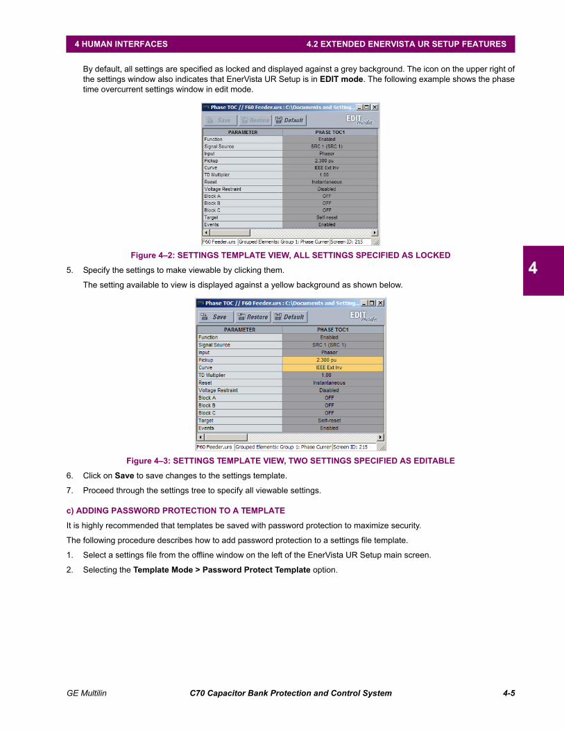
GE Multilin C70 Capacitor Bank Protection and Control System 4-5
4 HUMAN INTERFACES 4.2 EXTENDED ENERVISTA UR SETUP FEATURES
4
By default, all settings are specified as locked and displayed against a grey background. The icon on the upper right ofthe settings window also indicates that EnerVista UR Setup is in EDIT mode. The following example shows the phasetime overcurrent settings window in edit mode.
Figure 4–2: SETTINGS TEMPLATE VIEW, ALL SETTINGS SPECIFIED AS LOCKED
5. Specify the settings to make viewable by clicking them.
The setting available to view is displayed against a yellow background as shown below.
Figure 4–3: SETTINGS TEMPLATE VIEW, TWO SETTINGS SPECIFIED AS EDITABLE
6. Click on Save to save changes to the settings template.
7. Proceed through the settings tree to specify all viewable settings.
c) ADDING PASSWORD PROTECTION TO A TEMPLATE
It is highly recommended that templates be saved with password protection to maximize security.
The following procedure describes how to add password protection to a settings file template.
1. Select a settings file from the offline window on the left of the EnerVista UR Setup main screen.
2. Selecting the Template Mode > Password Protect Template option.

4-6 C70 Capacitor Bank Protection and Control System GE Multilin
4.2 EXTENDED ENERVISTA UR SETUP FEATURES 4 HUMAN INTERFACES
4
The software prompts for a template password. This password must be at least four characters in length.
3. Enter and re-enter the new password, then click OK to continue.
The settings file template is now secured with password protection.
When templates are created for online settings, the password is added during the initial template creation step. Itdoes not need to be added after the template is created.
d) VIEWING THE SETTINGS TEMPLATE
Once all necessary settings are specified for viewing, users are able to view the settings template on the online device orsettings file. There are two ways to specify the settings view with the settings template feature:
• Display only those settings available for editing
• Display all settings, with settings not available for editing greyed-out
Use the following procedure to only display settings available for editing:
1. Select an installed device or a settings file from the tree menu on the left of the EnerVista UR Setup main screen.
2. Apply the template by selecting the Template Mode > View In Template Mode option.
3. Enter the template password then click OK to apply the template.
Once the template has been applied, users are limited to view and edit the settings specified by the template. The effect ofapplying the template to the phase time overcurrent settings is shown below.
Figure 4–4: APPLYING TEMPLATES VIA THE VIEW IN TEMPLATE MODE COMMAND
NOTE
Phase time overcurrent settings window without template applied.
Phase time overcurrent window with template applied via
the command.
The template specifies that only the and
settings be available.
Template Mode > View In Template Mode
Pickup Curve
842858A1.CDR

GE Multilin C70 Capacitor Bank Protection and Control System 4-7
4 HUMAN INTERFACES 4.2 EXTENDED ENERVISTA UR SETUP FEATURES
4
Viewing the settings in template mode also modifies the settings tree, showing only the settings categories that containeditable settings. The effect of applying the template to a typical settings tree view is shown below.
Figure 4–5: APPLYING TEMPLATES VIA THE VIEW IN TEMPLATE MODE SETTINGS COMMAND
Use the following procedure to display settings available for editing and settings locked by the template.
1. Select an installed device or a settings file from the tree menu on the left of the EnerVista UR Setup main screen.
2. Apply the template by selecting the Template Mode > View All Settings option.
3. Enter the template password then click OK to apply the template.
Once the template has been applied, users are limited to edit the settings specified by the template, but all settings areshown. The effect of applying the template to the phase time overcurrent settings is shown below.
Figure 4–6: APPLYING TEMPLATES VIA THE VIEW ALL SETTINGS COMMAND
e) REMOVING THE SETTINGS TEMPLATE
It can be necessary at some point to remove a settings template. Once a template is removed, it cannot be reapplied and itis necessary to define a new settings template.
1. Select an installed device or settings file from the tree menu on the left of the EnerVista UR Setup main screen.
2. Select the Template Mode > Remove Settings Template option.
3. Enter the template password and click OK to continue.
Typical settings tree view without template applied. Typical settings tree view with template applied via
the
command.
Template Mode > View In Template Mode
842860A1.CDR
Phase time overcurrent settings window without template applied. Phase time overcurrent window with template applied via
the command.
The template specifies that only the and
settings be available.
Template Mode > View All Settings
Pickup Curve
842859A1.CDR

4-8 C70 Capacitor Bank Protection and Control System GE Multilin
4.2 EXTENDED ENERVISTA UR SETUP FEATURES 4 HUMAN INTERFACES
4
4. Verify one more time that you want to remove the template by clicking Yes.
The EnerVista software removes all template information and all settings are available.
4.2.2 SECURING AND LOCKING FLEXLOGIC EQUATIONS
The UR allows users to secure parts or all of a FlexLogic equation, preventing unauthorized viewing or modification of criti-cal FlexLogic applications. This is accomplished using the settings template feature to lock individual entries within Flex-Logic equations.
Secured FlexLogic equations remain secure when files are sent to and retrieved from any UR-series device.
a) LOCKING FLEXLOGIC EQUATION ENTRIES
The following procedure describes how to lock individual entries of a FlexLogic equation.
1. Right-click the settings file or online device and select the Template Mode > Create Template item to enable the set-tings template feature.
2. Select the FlexLogic > FlexLogic Equation Editor settings menu item.
By default, all FlexLogic entries are specified as viewable and displayed against a yellow background. The icon on theupper right of the window also indicates that EnerVista UR Setup is in EDIT mode.
3. Specify which entries to lock by clicking on them.
The locked entries are displayed against a grey background as shown in the example below.
Figure 4–7: LOCKING FLEXLOGIC ENTRIES IN EDIT MODE
4. Click on Save to save and apply changes to the settings template.
5. Select the Template Mode > View In Template Mode option to view the template.
6. Apply a password to the template then click OK to secure the FlexLogic equation.

GE Multilin C70 Capacitor Bank Protection and Control System 4-9
4 HUMAN INTERFACES 4.2 EXTENDED ENERVISTA UR SETUP FEATURES
4
Once the template has been applied, users are limited to view and edit the FlexLogic entries not locked by the template.The effect of applying the template to the FlexLogic entries in the above procedure is shown below.
Figure 4–8: LOCKING FLEXLOGIC ENTRIES THROUGH SETTING TEMPLATES
The FlexLogic entries are also shown as locked in the graphical view (as shown below) and on the front panel display.
Figure 4–9: SECURED FLEXLOGIC IN GRAPHICAL VIEW
b) LOCKING FLEXLOGIC EQUATIONS TO A SERIAL NUMBER
A settings file and associated FlexLogic equations can also be locked to a specific UR serial number. Once the desiredFlexLogic entries in a settings file have been secured, use the following procedure to lock the settings file to a specific serialnumber.
1. Select the settings file in the offline window.
2. Right-click on the file and select the Edit Settings File Properties item.
Typical FlexLogic™ entries without template applied. Typical locked with template via
the command.Template Mode > View In Template Mode
FlexLogic™ entries
842861A1.CDR
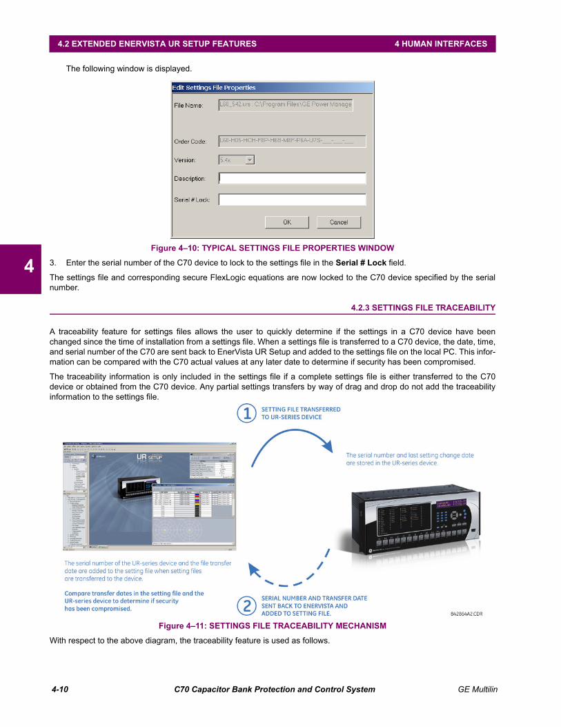
4-10 C70 Capacitor Bank Protection and Control System GE Multilin
4.2 EXTENDED ENERVISTA UR SETUP FEATURES 4 HUMAN INTERFACES
4
The following window is displayed.
Figure 4–10: TYPICAL SETTINGS FILE PROPERTIES WINDOW
3. Enter the serial number of the C70 device to lock to the settings file in the Serial # Lock field.
The settings file and corresponding secure FlexLogic equations are now locked to the C70 device specified by the serialnumber.
4.2.3 SETTINGS FILE TRACEABILITY
A traceability feature for settings files allows the user to quickly determine if the settings in a C70 device have beenchanged since the time of installation from a settings file. When a settings file is transferred to a C70 device, the date, time,and serial number of the C70 are sent back to EnerVista UR Setup and added to the settings file on the local PC. This infor-mation can be compared with the C70 actual values at any later date to determine if security has been compromised.
The traceability information is only included in the settings file if a complete settings file is either transferred to the C70device or obtained from the C70 device. Any partial settings transfers by way of drag and drop do not add the traceabilityinformation to the settings file.
Figure 4–11: SETTINGS FILE TRACEABILITY MECHANISM
With respect to the above diagram, the traceability feature is used as follows.
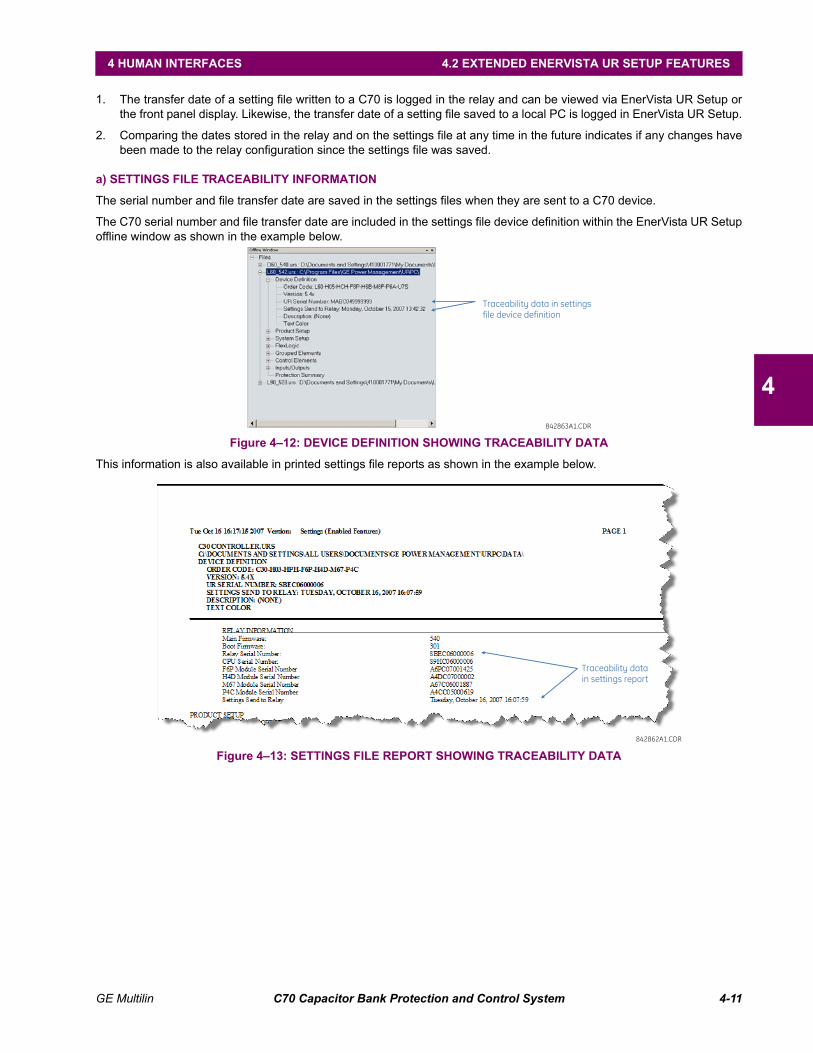
GE Multilin C70 Capacitor Bank Protection and Control System 4-11
4 HUMAN INTERFACES 4.2 EXTENDED ENERVISTA UR SETUP FEATURES
4
1. The transfer date of a setting file written to a C70 is logged in the relay and can be viewed via EnerVista UR Setup orthe front panel display. Likewise, the transfer date of a setting file saved to a local PC is logged in EnerVista UR Setup.
2. Comparing the dates stored in the relay and on the settings file at any time in the future indicates if any changes havebeen made to the relay configuration since the settings file was saved.
a) SETTINGS FILE TRACEABILITY INFORMATION
The serial number and file transfer date are saved in the settings files when they are sent to a C70 device.
The C70 serial number and file transfer date are included in the settings file device definition within the EnerVista UR Setupoffline window as shown in the example below.
Figure 4–12: DEVICE DEFINITION SHOWING TRACEABILITY DATA
This information is also available in printed settings file reports as shown in the example below.
Figure 4–13: SETTINGS FILE REPORT SHOWING TRACEABILITY DATA
Traceability data in settings
file device definition
842863A1.CDR
Traceability data
in settings report
842862A1.CDR

4-12 C70 Capacitor Bank Protection and Control System GE Multilin
4.2 EXTENDED ENERVISTA UR SETUP FEATURES 4 HUMAN INTERFACES
4
b) ONLINE DEVICE TRACEABILITY INFORMATION
The C70 serial number and file transfer date are available for an online device through the actual values. Select the ActualValues > Product Info > Model Information menu item within the EnerVista UR Setup online window as shown in theexample below.
Figure 4–14: TRACEABILITY DATA IN ACTUAL VALUES WINDOW
This information is also available from the front panel display through the following actual values:
ACTUAL VALUES PRODUCT INFO MODEL INFORMATION SERIAL NUMBER
ACTUAL VALUES PRODUCT INFO MODEL INFORMATION LAST SETTING CHANGE
c) ADDITIONAL TRACEABILITY RULES
The following additional rules apply for the traceability feature
• If the user changes any settings within the settings file in the offline window, then the traceability information isremoved from the settings file.
• If the user creates a new settings file, then no traceability information is included in the settings file.
• If the user converts an existing settings file to another revision, then any existing traceability information is removedfrom the settings file.
• If the user duplicates an existing settings file, then any traceability information is transferred to the duplicate settingsfile.
Traceability data in online
device actual values page
842865A1.CDR

GE Multilin C70 Capacitor Bank Protection and Control System 4-13
4 HUMAN INTERFACES 4.3 FACEPLATE INTERFACE
4
4.3FACEPLATE INTERFACE 4.3.1 FACEPLATE
a) ENHANCED FACEPLATE
The front panel interface is one of two supported interfaces, the other interface being EnerVista UR Setup software. Thefront panel interface consists of LED panels, an RS232 port, keypad, LCD display, control pushbuttons, and optional user-programmable pushbuttons.
The faceplate is hinged to allow easy access to the removable modules.
Figure 4–15: UR-SERIES ENHANCED FACEPLATE
b) STANDARD FACEPLATE
There are two interfaces: the front panel interface and the EnerVista UR Setup software. The front panel interface consistsof LED panels, an RS232 port, keypad, LCD display, control pushbuttons, and optional user-programmable pushbuttons.
The faceplate is hinged to allow easy access to the removable modules. There is also a removable dust cover that fits overthe faceplate that must be removed in order to access the keypad panel. The following figure shows the horizontal arrange-ment of the faceplate panels.
Figure 4–16: UR-SERIES STANDARD HORIZONTAL FACEPLATE PANELS
Five column LED indicator panel
Display
User-programmable pushbuttons 1 to 16 842810A1.CDR
Keypad
Front panel
RS232 port
LED panel 1 LED panel 2
Display
User-programmablepushbuttons 1 to 12 Keypad
Front panelRS232 port
Small user-programmable(control) pushbuttons 1 to 7
LED panel 3
827801A .
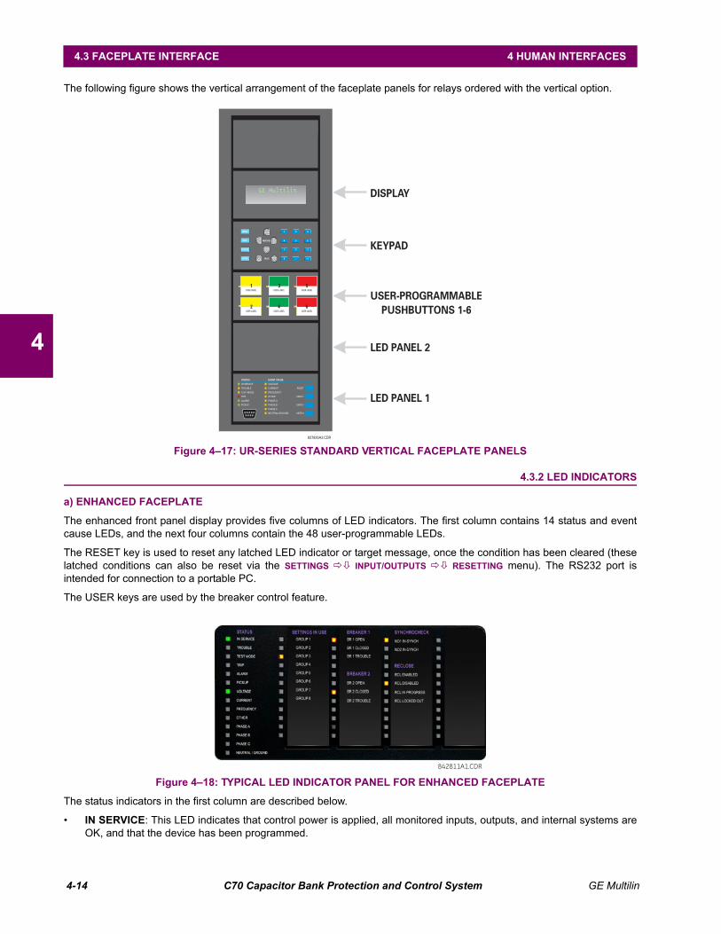
4-14 C70 Capacitor Bank Protection and Control System GE Multilin
4.3 FACEPLATE INTERFACE 4 HUMAN INTERFACES
4
The following figure shows the vertical arrangement of the faceplate panels for relays ordered with the vertical option.
Figure 4–17: UR-SERIES STANDARD VERTICAL FACEPLATE PANELS
4.3.2 LED INDICATORS
a) ENHANCED FACEPLATE
The enhanced front panel display provides five columns of LED indicators. The first column contains 14 status and eventcause LEDs, and the next four columns contain the 48 user-programmable LEDs.
The RESET key is used to reset any latched LED indicator or target message, once the condition has been cleared (theselatched conditions can also be reset via the SETTINGS INPUT/OUTPUTS RESETTING menu). The RS232 port isintended for connection to a portable PC.
The USER keys are used by the breaker control feature.
Figure 4–18: TYPICAL LED INDICATOR PANEL FOR ENHANCED FACEPLATE
The status indicators in the first column are described below.
• IN SERVICE: This LED indicates that control power is applied, all monitored inputs, outputs, and internal systems areOK, and that the device has been programmed.
842811A1.CDR

GE Multilin C70 Capacitor Bank Protection and Control System 4-15
4 HUMAN INTERFACES 4.3 FACEPLATE INTERFACE
4
• TROUBLE: This LED indicates that the relay has detected an internal problem.
• TEST MODE: This LED indicates that the relay is in test mode.
• TRIP: This LED indicates that the FlexLogic operand serving as a trip switch has operated. This indicator alwayslatches; as such, a reset command must be initiated to allow the latch to be reset.
• ALARM: This LED indicates that the FlexLogic operand serving as an alarm switch has operated. This indicator isnever latched.
• PICKUP: This LED indicates that an element is picked up. This indicator is never latched.
The event cause indicators in the first column are described below.
Events cause LEDs are turned on or off by protection elements that have their respective target setting selected as either“Enabled” or “Latched”. If a protection element target setting is “Enabled”, then the corresponding event cause LEDsremain on as long as operate operand associated with the element remains asserted. If a protection element target settingis “Latched”, then the corresponding event cause LEDs turn on when the operate operand associated with the element isasserted and remain on until the RESET button on the front panel is pressed after the operand is reset.
All elements that are able to discriminate faulted phases can independently turn off or on the phase A, B or C LEDs. Thisincludes phase instantaneous overcurrent, phase undervoltage, etc. This means that the phase A, B, and C operate oper-ands for individual protection elements are ORed to turn on or off the phase A, B or C LEDs.
• VOLTAGE: This LED indicates voltage was involved.
• CURRENT: This LED indicates current was involved.
• FREQUENCY: This LED indicates frequency was involved.
• OTHER: This LED indicates a composite function was involved.
• PHASE A: This LED indicates phase A was involved.
• PHASE B: This LED indicates phase B was involved.
• PHASE C: This LED indicates phase C was involved.
• NEUTRAL/GROUND: This LED indicates that neutral or ground was involved.
The user-programmable LEDs consist of 48 amber LED indicators in four columns. The operation of these LEDs is user-defined. Support for applying a customized label beside every LED is provided. Default labels are shipped in the label pack-age of every C70, together with custom templates. The default labels can be replaced by user-printed labels.
User customization of LED operation is of maximum benefit in installations where languages other than English are used tocommunicate with operators. Refer to the User-programmable LEDs section in chapter 5 for the settings used to programthe operation of the LEDs on these panels.
b) STANDARD FACEPLATE
The standard faceplate consists of three panels with LED indicators, keys, and a communications port. The RESET key isused to reset any latched LED indicator or target message, once the condition has been cleared (these latched conditionscan also be reset via the SETTINGS INPUT/OUTPUTS RESETTING menu). The RS232 port is for connection to a com-puter.
The USER keys are used by the breaker control feature.
Figure 4–19: LED PANEL 1
PICKUP
ALARM
TRIP
TEST MODE
TROUBLE
IN SERVICE
STATUS
USER 3
USER 2
USER 1
RESET
NEUTRAL/GROUND
PHASE C
PHASE B
PHASE A
OTHER
FREQUENCY
CURRENT
VOLTAGE
EVENT CAUSE
842781A1.CDR

4-16 C70 Capacitor Bank Protection and Control System GE Multilin
4.3 FACEPLATE INTERFACE 4 HUMAN INTERFACES
4
STATUS INDICATORS:
• IN SERVICE: Indicates that control power is applied; all monitored inputs/outputs and internal systems are OK; therelay has been programmed.
• TROUBLE: Indicates that the relay has detected an internal problem.
• TEST MODE: Indicates that the relay is in test mode.
• TRIP: Indicates that the selected FlexLogic operand serving as a Trip switch has operated. This indicator alwayslatches; the reset command must be initiated to allow the latch to be reset.
• ALARM: Indicates that the selected FlexLogic operand serving as an Alarm switch has operated. This indicator isnever latched.
• PICKUP: Indicates that an element is picked up. This indicator is never latched.
EVENT CAUSE INDICATORS:
Events cause LEDs are turned on or off by protection elements that have their respective target setting selected as either“Enabled” or “Latched”. If a protection element target setting is “Enabled”, then the corresponding event cause LEDsremain on as long as operate operand associated with the element remains asserted. If a protection element target settingis “Latched”, then the corresponding event cause LEDs turn on when the operate operand associated with the element isasserted and remain on until the RESET button on the front panel is pressed after the operand is reset.
All elements that are able to discriminate faulted phases can independently turn off or on the phase A, B or C LEDs. Thisincludes phase instantaneous overcurrent, phase undervoltage, etc. This means that the phase A, B, and C operate oper-ands for individual protection elements are ORed to turn on or off the phase A, B or C LEDs.
• VOLTAGE: Indicates voltage was involved.
• CURRENT: Indicates current was involved.
• FREQUENCY: Indicates frequency was involved.
• OTHER: Indicates a composite function was involved.
• PHASE A: Indicates phase A was involved.
• PHASE B: Indicates phase B was involved.
• PHASE C: Indicates phase C was involved.
• NEUTRAL/GROUND: Indicates that neutral or ground was involved.
USER-PROGRAMMABLE INDICATORS:
The second and third provide 48 amber LED indicators whose operation is controlled by the user. Support for applying acustomized label beside every LED is provided.
User customization of LED operation is of maximum benefit in installations where languages other than English are used tocommunicate with operators. Refer to the User-programmable LEDs section in chapter 5 for the settings used to programthe operation of the LEDs on these panels.
Figure 4–20: LED PANELS 2 AND 3 (INDEX TEMPLATE)
DEFAULT LABELS FOR LED PANEL 2:
The default labels are intended to represent:
USER-PROGRAMMABLE LEDS USER-PROGRAMMABLE LEDS
842782A1.CDR

GE Multilin C70 Capacitor Bank Protection and Control System 4-17
4 HUMAN INTERFACES 4.3 FACEPLATE INTERFACE
4
• GROUP 1...6: The illuminated GROUP is the active settings group.
The relay is shipped with the default label for the LED panel 2. The LEDs, however, are not pre-programmed. To match thepre-printed label, the LED settings must be entered as shown in the User-programmable LEDs section of chapter 5. TheLEDs are fully user-programmable. The default labels can be replaced by user-printed labels for both panels as explainedin the following section.
Figure 4–21: LED PANEL 2 (DEFAULT LABELS)
4.3.3 CUSTOM LABELING OF LEDS
a) ENHANCED FACEPLATE
The following procedure requires these pre-requisites:
• EnerVista UR Setup software is installed and operational
• The C70 settings have been saved to a settings file
• The C70 front panel label cutout sheet (GE Multilin part number 1006-0047) has been downloaded from http://www.gedigitalenergy.com/products/support/ur/URLEDenhanced.doc and printed
• Small-bladed knife
To create custom LED labels for the enhanced front panel display:
1. Start the EnerVista UR Setup software.
2. Select the Front Panel Report item at the bottom of the menu tree for the settings file. The front panel report windowdisplays.
Figure 4–22: FRONT PANEL REPORT WINDOW
SETTINGS IN USE
842783A1.CDR

4-18 C70 Capacitor Bank Protection and Control System GE Multilin
4.3 FACEPLATE INTERFACE 4 HUMAN INTERFACES
4
3. Enter the text to appear next to each LED and above each user-programmable pushbuttons in the fields provided.
4. Feed the C70 front panel label cutout sheet into a printer and press the Print button in the front panel report window.
5. When printing is complete, fold the sheet along the perforated lines and punch out the labels.
6. Remove the C70 label insert tool from the package and bend the tabs as described in the following procedures. Thesetabs are used for removal of the default and custom LED labels.
It is important that the tool be used EXACTLY as shown below, with the printed side containing the GE part numberfacing the user.
The label package shipped with every C70 contains the three default labels shown below, the custom label template sheet,and the label removal tool.
If the default labels are suitable for your application, insert them in the appropriate slots and program the LEDs to matchthem. If you require custom labels, follow the procedures below to remove the original labels and insert the new ones.
The following procedure describes how to setup and use the label removal tool.
1. Bend the tabs at the left end of the tool upwards as shown below.
2. Bend the tab at the center of the tool tail as shown below.
The following procedure describes how to remove the LED labels from the C70 enhanced front panel and insert the customlabels.
NOTE
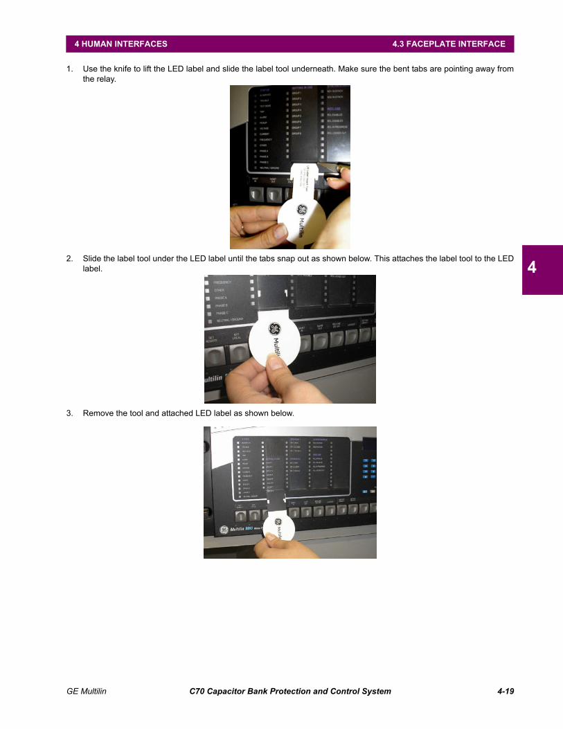
GE Multilin C70 Capacitor Bank Protection and Control System 4-19
4 HUMAN INTERFACES 4.3 FACEPLATE INTERFACE
4
1. Use the knife to lift the LED label and slide the label tool underneath. Make sure the bent tabs are pointing away fromthe relay.
2. Slide the label tool under the LED label until the tabs snap out as shown below. This attaches the label tool to the LEDlabel.
3. Remove the tool and attached LED label as shown below.

4-20 C70 Capacitor Bank Protection and Control System GE Multilin
4.3 FACEPLATE INTERFACE 4 HUMAN INTERFACES
4
4. Slide the new LED label inside the pocket until the text is properly aligned with the LEDs, as shown below.
The following procedure describes how to remove the user-programmable pushbutton labels from the C70 enhanced frontpanel and insert the custom labels.
1. Use the knife to lift the pushbutton label and slide the tail of the label tool underneath, as shown below. Make sure thebent tab is pointing away from the relay.
2. Slide the label tool under the user-programmable pushbutton label until the tabs snap out as shown below. Thisattaches the label tool to the user-programmable pushbutton label.

GE Multilin C70 Capacitor Bank Protection and Control System 4-21
4 HUMAN INTERFACES 4.3 FACEPLATE INTERFACE
4
3. Remove the tool and attached user-programmable pushbutton label as shown below.
4. Slide the new user-programmable pushbutton label inside the pocket until the text is properly aligned with the buttons,as shown below.
b) STANDARD FACEPLATE
Custom labeling of an LED-only panel is facilitated through a Microsoft Word file available from the following URL:
http://www.gedigitalenergy.com/products/support/ur/GET-8494A.doc
This file provides templates and instructions for creating appropriate labeling for the LED panel. The following proceduresare contained in the downloadable file. The panel templates provide relative LED locations and located example text (x)edit boxes. The following procedure demonstrates how to install/uninstall the custom panel labeling.

4-22 C70 Capacitor Bank Protection and Control System GE Multilin
4.3 FACEPLATE INTERFACE 4 HUMAN INTERFACES
4
1. Remove the clear Lexan Front Cover (GE Multilin part number: 1501-0014).
2. Pop out the LED module and/or the blank module with a screwdriver as shown below. Be careful not to damage theplastic covers.
3. Place the left side of the customized module back to the front panel frame, then snap back the right side.
4. Put the clear Lexan front cover back into place.
The following items are required to customize the C70 display module:
• Black and white or color printer (color preferred)
• Microsoft Word 97 or later software for editing the template
• 1 each of: 8.5" x 11" white paper, exacto knife, ruler, custom display module (GE Multilin Part Number: 1516-0069),and a custom module cover (GE Multilin Part Number: 1502-0015)
The following procedure describes how to customize the C70 display module:
1. Open the LED panel customization template with Microsoft Word. Add text in places of the LED x text placeholders onthe template(s). Delete unused place holders as required.
2. When complete, save the Word file to your computer for future use.
3. Print the template(s) to a local printer.
4. From the printout, cut-out the Background Template from the three windows, using the cropmarks as a guide.
5. Put the Background Template on top of the custom display module (GE Multilin Part Number: 1513-0069) and snap theclear custom module cover (GE Multilin Part Number: 1502-0015) over it and the templates.
4.3.4 DISPLAY
All messages are displayed on a backlit liquid crystal display (LCD) to make them visible under poor lighting conditions.While the keypad and display are not actively being used, the display defaults to user-defined messages. Any high-priorityevent-driven message automatically overrides the default message and appears on the display.
4.3.5 KEYPAD
Display messages are organized into pages under the following headings: actual values, settings, commands, and targets.The MENU key navigates through these pages. Each heading page is divided further into logical subgroups.
Push in
and gently lift
up the cover.
F60 FEEDER MANAGEMENT RELAYF60 FEEDER MANAGEMENT RELAYF60 FEEDER MANAGEMENT RELAYF60 FEEDER MANAGEMENT RELAYR
842771A1.CDR
F60 FEEDER MANAGEMENT RELAY
( LED MODULE ) ( BLANK MODULE )
R
842722A1.CDR

GE Multilin C70 Capacitor Bank Protection and Control System 4-23
4 HUMAN INTERFACES 4.3 FACEPLATE INTERFACE
4
The MESSAGE keys navigate through the subgroups. The VALUE keys increment or decrement numerical setting valueswhen in programming mode. These keys also scroll through alphanumeric values in the text edit mode. Alternatively, val-ues can be entered with the numeric keypad.
The decimal key initiates and advances to the next character in text edit mode or enters a decimal point.
The HELP key can be pressed at any time for context-sensitive help messages.
The ENTER key stores altered setting values.
4.3.6 BREAKER CONTROL
a) INTRODUCTION
The C70 can interface with associated circuit breakers. In many cases the application monitors the state of the breaker, thatcan be presented on faceplate LEDs, along with a breaker trouble indication. Breaker operations can be manually initiatedfrom faceplate keypad or automatically initiated from a FlexLogic operand. A setting is provided to assign names to eachbreaker; this user-assigned name is used for the display of related flash messages. These features are provided for twobreakers; the user can use only those portions of the design relevant to a single breaker, which must be breaker 1.
For the following discussion it is assumed the SETTINGS SYSTEM SETUP BREAKERS BREAKER 1(2) BREAKER
FUNCTION setting is "Enabled" for each breaker.
b) CONTROL MODE SELECTION AND MONITORING
Installations can require that a breaker is operated in the three-pole only mode (3-pole), or in the one and three-pole (1-pole) mode, selected by setting. If the mode is selected as three-pole, a single input tracks the breaker open or closed posi-tion. If the mode is selected as one-pole, all three breaker pole states must be input to the relay. These inputs must be inagreement to indicate the position of the breaker.
For the following discussion it is assumed the SETTINGS SYSTEM SETUP BREAKERS BREAKER 1(2) BREAKER
1(2) PUSH BUTTON CONTROL setting is “Enabled” for each breaker.
c) FACEPLATE (USER KEY) CONTROL
After the 30 minute interval during which command functions are permitted after a correct command password, the usercannot open or close a breaker via the keypad. The following discussions begin from the not-permitted state.
d) CONTROL OF TWO BREAKERS
For the following example setup, the (Name) field represents the user-programmed variable name.
For this application (setup shown below), the relay is connected and programmed for both breaker 1 and breaker 2. TheUSER 1 key performs the selection of which breaker is to be operated by the USER 2 and USER 3 keys. The USER 2 keyis used to manually close the breaker and the USER 3 key is used to manually open the breaker.

4-24 C70 Capacitor Bank Protection and Control System GE Multilin
4.3 FACEPLATE INTERFACE 4 HUMAN INTERFACES
4
e) CONTROL OF ONE BREAKER
For this application the relay is connected and programmed for breaker 1 only. Operation for this application is identical tothat described above for two breakers.
4.3.7 MENUS
a) NAVIGATION
Press the MENU key to select a header display page (top-level menu). The header title appears momentarily followed by aheader display page menu item. Each press of the MENU key advances through the following main heading pages:
• Actual values
• Settings
• Commands
• Targets
• User displays (when enabled)
ENTER COMMANDPASSWORD
This message appears when the USER 1, USER 2, or USER 3 key is pressed and aCOMMAND PASSWORD is required; i.e. if COMMAND PASSWORD is enabled and no com-mands have been issued within the last 30 minutes.
Press USER 1To Select Breaker
This message appears if the correct password is entered or if none is required. This mes-sage displays for 30 seconds or until the USER 1 key is pressed again.
BKR1-(Name) SELECTEDUSER 2=CLS/USER 3=OP
This message is displayed after the USER 1 key is pressed for the second time. Threepossible actions can be performed from this state within 30 seconds as per items (1), (2)and (3) below:
(1)
USER 2 OFF/ONTo Close BKR1-(Name)
If the USER 2 key is pressed, this message appears for 20 seconds. If the USER 2 key ispressed again within that time, a signal is created that can be programmed to operate anoutput relay to close breaker 1.
(2)
USER 3 OFF/ONTo Open BKR1-(Name)
If the USER 3 key is pressed, this message appears for 20 seconds. If the USER 3 key ispressed again within that time, a signal is created that can be programmed to operate anoutput relay to open breaker 1.
(3)
BKR2-(Name) SELECTEDUSER 2=CLS/USER 3=OP
If the USER 1 key is pressed at this step, this message appears showing that a differentbreaker is selected. Three possible actions can be performed from this state as per (1),(2) and (3). Repeatedly pressing the USER 1 key alternates between available breakers.Pressing keys other than USER 1, 2, or 3 at any time aborts the breaker control function.

GE Multilin C70 Capacitor Bank Protection and Control System 4-25
4 HUMAN INTERFACES 4.3 FACEPLATE INTERFACE
4
b) HIERARCHY
The setting and actual value messages are arranged hierarchically. The header display pages are indicated by doublescroll bar characters (), while sub-header pages are indicated by single scroll bar characters (). The header displaypages represent the highest level of the hierarchy and the sub-header display pages fall below this level. The MESSAGEUP and DOWN keys move within a group of headers, sub-headers, setting values, or actual values. Continually pressingthe MESSAGE RIGHT key from a header display displays specific information for the header category. Conversely, contin-ually pressing the MESSAGE LEFT key from a setting value or actual value display returns to the header display.
c) EXAMPLE MENU NAVIGATION
HIGHEST LEVEL LOWEST LEVEL (SETTING VALUE)
SETTINGS PRODUCT SETUP
PASSWORD SECURITY
ACCESS LEVEL:Restricted
SETTINGS SYSTEM SETUP
ACTUAL VALUES STATUS
Press the MENU key until the header for the first Actual Values page appears. Thispage contains system and relay status information. Repeatedly press the MESSAGEkeys to display the other actual value headers.
SETTINGS PRODUCT SETUP
Press the MENU key until the header for the first page of Settings appears. This pagecontains settings to configure the relay.
SETTINGS SYSTEM SETUP
Press the MESSAGE DOWN key to move to the next Settings page. This page con-tains settings for System Setup. Repeatedly press the MESSAGE UP and DOWNkeys to display the other setting headers and then back to the first Settings pageheader.
PASSWORD SECURITY
From the Settings page one header (Product Setup), press the MESSAGE RIGHTkey once to display the first sub-header (Password Security).
ACCESS LEVEL:Restricted
Press the MESSAGE RIGHT key once more and this will display the first setting forPassword Security. Pressing the MESSAGE DOWN key repeatedly will display theremaining setting messages for this sub-header.
PASSWORD SECURITY
Press the MESSAGE LEFT key once to move back to the first sub-header message.
DISPLAY PROPERTIES
Pressing the MESSAGE DOWN key displays the second setting sub-header associ-ated with the Product Setup header.
FLASH MESSAGETIME: 1.0 s
Press the MESSAGE RIGHT key once more to display the first setting for DisplayProperties.
DEFAULT MESSAGEINTENSITY: 25%
To view the remaining settings associated with the Display Properties subheader,repeatedly press the MESSAGE DOWN key. The last message appears as shown.

4-26 C70 Capacitor Bank Protection and Control System GE Multilin
4.3 FACEPLATE INTERFACE 4 HUMAN INTERFACES
4
4.3.8 CHANGING SETTINGS
a) ENTERING NUMERICAL DATA
Each numerical setting has its own minimum, maximum, and increment value associated with it. These parameters definewhat values are acceptable for a setting.
Two methods of editing and storing a numerical setting value are available.
• 0 to 9 and decimal point: The relay numeric keypad works the same as that of any electronic calculator. A number isentered one digit at a time. The leftmost digit is entered first and the rightmost digit is entered last. Pressing the MES-SAGE LEFT key or pressing the ESCAPE key, returns the original value to the display.
• VALUE keys: The VALUE UP key increments the displayed value by the step value, up to the maximum value allowed.While at the maximum value, pressing the VALUE UP key again allows the setting selection to continue upward fromthe minimum value. The VALUE DOWN key decrements the displayed value by the step value, down to the minimumvalue. While at the minimum value, pressing the VALUE DOWN key again allows the setting selection to continuedownward from the maximum value.
b) ENTERING ENUMERATION DATA
Enumeration settings have data values which are part of a set, whose members are explicitly defined by a name. A set iscomprised of two or more members.
Enumeration type values are changed using the VALUE keys. The VALUE UP key displays the next selection while theVALUE DOWN key displays the previous selection.
c) ENTERING ALPHANUMERIC TEXT
Text settings have data values which are fixed in length, but user-defined in character. They can be upper case letters,lower case letters, numerals, and a selection of special characters.
FLASH MESSAGETIME: 1.0 s
For example, select the SETTINGS PRODUCT SETUP DISPLAY PROPERTIES FLASH
MESSAGE TIME setting.
MINIMUM: 0.5MAXIMUM: 10.0
Press the HELP key to view the minimum and maximum values. Press the HELP keyagain to view the next context sensitive help message.
FLASH MESSAGETIME: 2.5 s
As an example, set the flash message time setting to 2.5 seconds. Press the appropriatenumeric keys in the sequence “2 . 5". The display message changes as the digits arebeing entered.
NEW SETTINGHAS BEEN STORED
Until ENTER is pressed, editing changes are not registered by the relay. Therefore, pressENTER to store the new value in memory. This flash message momentarily appears asconfirmation of the storing process. Numerical values which contain decimal places arerounded-off if more decimal place digits are entered than specified by the step value.
ACCESS LEVEL:Restricted
For example, the selections available for ACCESS LEVEL are "Restricted", "Command","Setting", and "Factory Service".
ACCESS LEVEL:Setting
If the ACCESS LEVEL needs to be "Setting", press the VALUE keys until the proper selec-tion is displayed. Press HELP at any time for the context sensitive help messages.
NEW SETTINGHAS BEEN STORED
Changes are not registered by the relay until the ENTER key is pressed. PressingENTER stores the new value in memory. This flash message momentarily appears asconfirmation of the storing process.

GE Multilin C70 Capacitor Bank Protection and Control System 4-27
4 HUMAN INTERFACES 4.3 FACEPLATE INTERFACE
4
There are several places where text messages can be programmed to allow the relay to be customized for specific applica-tions. One example is the Message Scratchpad. Use the following procedure to enter alphanumeric text messages.
For example: to enter the text, “Breaker #1”.
1. Press the decimal point to enter text edit mode.
2. Press the VALUE keys until the character 'B' appears; press the decimal key to advance the cursor to the next position.
3. Repeat step 2 for the remaining characters: r,e,a,k,e,r, ,#,1.
4. Press ENTER to store the text.
5. If you have any problem, press HELP to view context sensitive help. Flash messages appear sequentially for severalseconds each. For the case of a text setting message, pressing HELP displays how to edit and store new values.
d) ACTIVATING THE RELAY
To change the RELAY SETTINGS: "Not Programmed" mode to "Programmed", proceed as follows:
1. Press the MENU key until the SETTINGS header flashes momentarily and the PRODUCT SETUP message appears on thedisplay.
2. Press the MESSAGE RIGHT key until the PASSWORD SECURITY message appears on the display.
3. Press the MESSAGE DOWN key until the INSTALLATION message appears on the display.
4. Press the MESSAGE RIGHT key until the RELAY SETTINGS: Not Programmed message is displayed.
5. After the RELAY SETTINGS: Not Programmed message appears on the display, press the VALUE keys change theselection to "Programmed".
6. Press the ENTER key.
7. When the "NEW SETTING HAS BEEN STORED" message appears, the relay is in "Programmed" state and the InService LED turns on.
e) ENTERING INITIAL PASSWORDS
The C70 supports password entry from a local or remote connection.
RELAY SETTINGS:Not Programmed
When the relay is powered up, the Trouble LED is on, the In Service LED off, and thismessage displayed, indicating the relay is in the "Not Programmed" state and is safe-guarding (output relays blocked) against the installation of a relay whose settings havenot been entered. This message remains until the relay is explicitly put in the "Pro-grammed" state.
SETTINGS
SETTINGS PRODUCT SETUP
PASSWORD SECURITY
DISPLAY PROPERTIES
INSTALLATION
RELAY SETTINGS:Not Programmed
RELAY SETTINGS:Not Programmed
RELAY SETTINGS:Programmed
NEW SETTINGHAS BEEN STORED

4-28 C70 Capacitor Bank Protection and Control System GE Multilin
4.3 FACEPLATE INTERFACE 4 HUMAN INTERFACES
4
Local access is defined as any access to settings or commands via the faceplate interface. This includes both keypad entryand the faceplate RS232 connection. Remote access is defined as any access to settings or commands via any rear com-munications port. This includes both Ethernet and RS485 connections. Any changes to the local or remote passwordsenables this functionality.
To enter the initial setting (or command) password, proceed as follows:
1. Press the MENU key until the SETTINGS header flashes momentarily and the PRODUCT SETUP message appears on thedisplay.
2. Press the MESSAGE RIGHT key until the ACCESS LEVEL message appears on the display.
3. Press the MESSAGE DOWN key until the CHANGE LOCAL PASSWORDS message appears on the display.
4. Press the MESSAGE RIGHT key until the CHANGE SETTING PASSWORD or CHANGE COMMAND PASSWORD messageappears on the display.
5. After the CHANGE...PASSWORD message appears on the display, press the VALUE UP or DOWN key to change theselection to “Yes”.
6. Press the ENTER key and the display prompts you to ENTER NEW PASSWORD.
7. Type in a numerical password (up to 10 characters) and press the ENTER key.
8. When the VERIFY NEW PASSWORD is displayed, re-type in the same password and press ENTER.
9. When the NEW PASSWORD HAS BEEN STORED message appears, your new Setting (or Command) Password will beactive.
f) CHANGING EXISTING PASSWORD
To change an existing password, follow the instructions in the previous section with the following exception. A messageprompts you to type in the existing password (for each security level) before a new password can be entered.
In the event that a password has been lost (forgotten), submit the corresponding encrypted password from the PASSWORD
SECURITY menu to the Factory for decoding.
g) INVALID PASSWORD ENTRY
When an incorrect command or setting password has been entered via the faceplate interface three times within a 3-minutetime span, the LOCAL ACCESS DENIED FlexLogic operand is set to “On” and the C70 does not allow settings or commandlevel access via the faceplate interface for the next five minutes, or in the event that an incorrect Command Or Setting
PASSWORD SECURITY
ACCESS LEVEL:Restricted
CHANGE LOCAL PASSWORDS
CHANGE COMMANDPASSWORD: No
CHANGE SETTINGPASSWORD: No
ENCRYPTED COMMANDPASSWORD: ---------
ENCRYPTED SETTINGPASSWORD: ---------
CHANGE SETTINGPASSWORD: No
CHANGE SETTINGPASSWORD: Yes
ENTER NEWPASSWORD: ##########
VERIFY NEWPASSWORD: ##########
NEW PASSWORDHAS BEEN STORED

GE Multilin C70 Capacitor Bank Protection and Control System 4-29
4 HUMAN INTERFACES 4.3 FACEPLATE INTERFACE
4
password has been entered via the any external communications interface three times within a 3-minute time span, theREMOTE ACCESS DENIED FlexLogic operand is set to “On” and the C70 does not allow settings or command access via theany external communications interface for the next five minutes.
In the event that an incorrect Command or Setting password has been entered via the any external communications inter-face three times within a three-minute time span, the REMOTE ACCESS DENIED FlexLogic operand is set to “On” and theC70 does not allow Settings or Command access via the any external communications interface for the next ten minutes.The REMOTE ACCESS DENIED FlexLogic operand is set to “Off” after the expiration of the ten-minute timeout.

4-30 C70 Capacitor Bank Protection and Control System GE Multilin
4.3 FACEPLATE INTERFACE 4 HUMAN INTERFACES
4
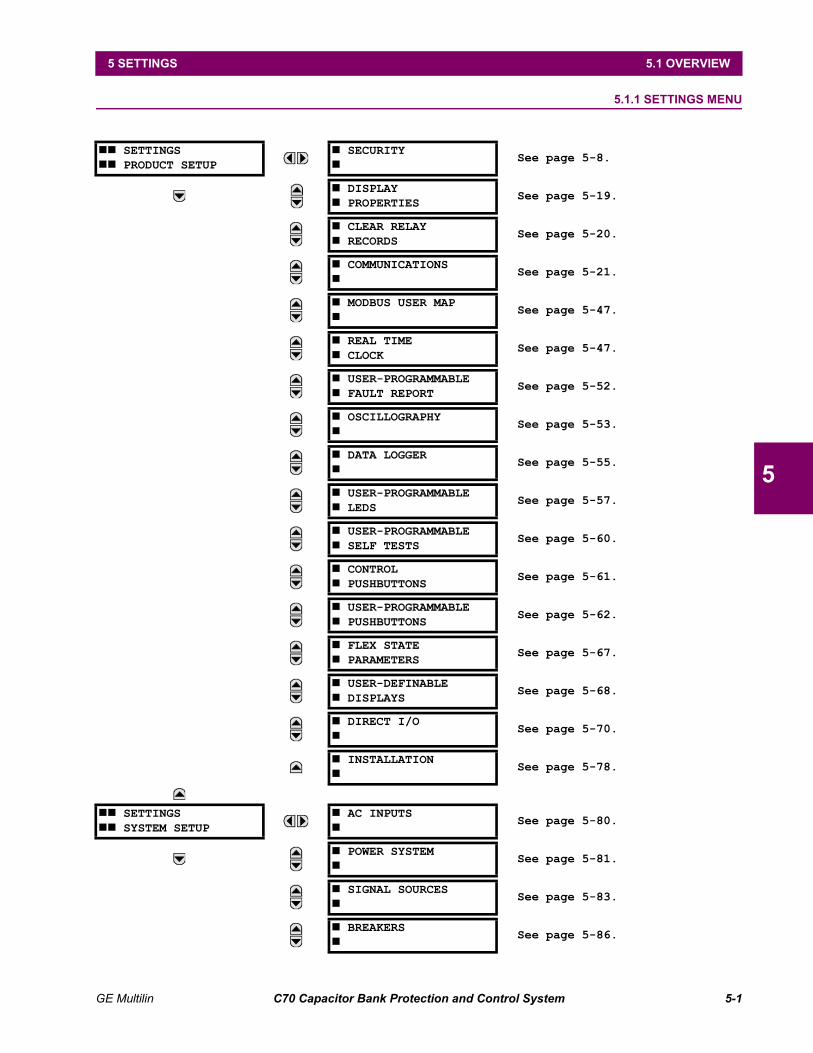
GE Multilin C70 Capacitor Bank Protection and Control System 5-1
5 SETTINGS 5.1 OVERVIEW
5
5 SETTINGS 5.1OVERVIEW 5.1.1 SETTINGS MENU
SETTINGS PRODUCT SETUP
SECURITY
See page 5-8.
DISPLAY PROPERTIES
See page 5-19.
CLEAR RELAY RECORDS
See page 5-20.
COMMUNICATIONS
See page 5-21.
MODBUS USER MAP
See page 5-47.
REAL TIME CLOCK
See page 5-47.
USER-PROGRAMMABLE FAULT REPORT
See page 5-52.
OSCILLOGRAPHY
See page 5-53.
DATA LOGGER
See page 5-55.
USER-PROGRAMMABLE LEDS
See page 5-57.
USER-PROGRAMMABLE SELF TESTS
See page 5-60.
CONTROL PUSHBUTTONS
See page 5-61.
USER-PROGRAMMABLE PUSHBUTTONS
See page 5-62.
FLEX STATE PARAMETERS
See page 5-67.
USER-DEFINABLE DISPLAYS
See page 5-68.
DIRECT I/O
See page 5-70.
INSTALLATION
See page 5-78.
SETTINGS SYSTEM SETUP
AC INPUTS
See page 5-80.
POWER SYSTEM
See page 5-81.
SIGNAL SOURCES
See page 5-83.
BREAKERS
See page 5-86.

5-2 C70 Capacitor Bank Protection and Control System GE Multilin
5.1 OVERVIEW 5 SETTINGS
5
SWITCHES
See page 5-90.
FLEXCURVES
See page 5-93.
SETTINGS FLEXLOGIC
FLEXLOGIC EQUATION EDITOR
See page 5-116.
FLEXLOGIC TIMERS
See page 5-116.
FLEXELEMENTS
See page 5-117.
NON-VOLATILE LATCHES
See page 5-121.
SETTINGS GROUPED ELEMENTS
SETTING GROUP 1
See page 5-122.
SETTING GROUP 2
SETTING GROUP 6
SETTINGS CONTROL ELEMENTS
TRIP BUS
See page 5-185.
SETTING GROUPS
See page 5-187.
SELECTOR SWITCH
See page 5-188.
TIME OF DAY TIMERS
See page 5-194.
CAPACITOR CONTROL
See page 5-195.
AUTOMATIC VOLTAGE REGULATOR
See page 5-200.
DIGITAL ELEMENTS
See page 5-205.
DIGITAL COUNTERS
See page 5-208.
MONITORING ELEMENTS
See page 5-210.
SETTINGS INPUTS / OUTPUTS
CONTACT INPUTS
See page 5-222.
VIRTUAL INPUTS
See page 5-224.

GE Multilin C70 Capacitor Bank Protection and Control System 5-3
5 SETTINGS 5.1 OVERVIEW
5
CONTACT OUTPUTS
See page 5-225.
VIRTUAL OUTPUTS
See page 5-227.
REMOTE DEVICES
See page 5-228.
REMOTE INPUTS
See page 5-229.
REMOTE DPS INPUTS
See page 5-230.
REMOTE OUTPUTS DNA BIT PAIRS
See page 5-230.
REMOTE OUTPUTS UserSt BIT PAIRS
See page 5-231.
RESETTING
See page 5-231.
DIRECT INPUTS
See page 5-232.
DIRECT OUTPUTS
See page 5-232.
IEC 61850 GOOSE ANALOGS
See page 5-235.
IEC 61850 GOOSE UINTEGERS
See page 5-236.
SETTINGS TRANSDUCER I/O
DCMA INPUTS
See page 5-237.
RTD INPUTS
See page 5-238.
DCMA OUTPUTS
See page 5-240.
SETTINGS TESTING
TEST MODEFUNCTION: Disabled
See page 5-243.
TEST MODE FORCING:On
See page 5-243.
FORCE CONTACT INPUTS
See page 5-244.
FORCE CONTACT OUTPUTS
See page 5-245.

5-4 C70 Capacitor Bank Protection and Control System GE Multilin
5.1 OVERVIEW 5 SETTINGS
5
5.1.2 INTRODUCTION TO ELEMENTS
In the design of UR relays, the term element is used to describe a feature that is based around a comparator. The compar-ator is provided with an input (or set of inputs) that is tested against a programmed setting (or group of settings) to deter-mine if the input is within the defined range that will set the output to logic 1, also referred to as setting the flag. A singlecomparator may make multiple tests and provide multiple outputs; for example, the time overcurrent comparator sets apickup flag when the current input is above the setting and sets an operate flag when the input current has been at a levelabove the pickup setting for the time specified by the time-current curve settings. All comparators use analog parameteractual values as the input.
The exception to the above rule are the digital elements, which use logic states as inputs.
Elements are arranged into two classes, grouped and control. Each element classed as a grouped element is provided withsix alternate sets of settings, in setting groups numbered 1 through 6. The performance of a grouped element is defined bythe setting group that is active at a given time. The performance of a control element is independent of the selected activesetting group.
The main characteristics of an element are shown on the element logic diagram. This includes the inputs, settings, fixedlogic, and the output operands generated (abbreviations used on scheme logic diagrams are defined in Appendix F).
Some settings for current and voltage elements are specified in per-unit (pu) calculated quantities:
pu quantity = (actual quantity) / (base quantity)
For current elements, the base quantity is the nominal secondary or primary current of the CT.
Where the current source is the sum of two CTs with different ratios, the base quantity will be the common secondary or pri-mary current to which the sum is scaled (that is, normalized to the larger of the two rated CT inputs). For example, if CT1 =300 / 5 A and CT2 = 100 / 5 A, then in order to sum these, CT2 is scaled to the CT1 ratio. In this case, the base quantity willbe 5 A secondary or 300 A primary.
For voltage elements the base quantity is the nominal primary voltage of the protected system which corresponds (basedon VT ratio and connection) to secondary VT voltage applied to the relay.
For example, on a system with a 13.8 kV nominal primary voltage and with 14400:120 V delta-connected VTs, the second-ary nominal voltage (1 pu) would be:
(EQ 5.1)
For wye-connected VTs, the secondary nominal voltage (1 pu) would be:
(EQ 5.2)
Many settings are common to most elements and are discussed below:
• FUNCTION setting: This setting programs the element to be operational when selected as “Enabled”. The factorydefault is “Disabled”. Once programmed to “Enabled”, any element associated with the function becomes active and alloptions become available.
• NAME setting: This setting is used to uniquely identify the element.
• SOURCE setting: This setting is used to select the parameter or set of parameters to be monitored.
• PICKUP setting: For simple elements, this setting is used to program the level of the measured parameter above orbelow which the pickup state is established. In more complex elements, a set of settings may be provided to define therange of the measured parameters which will cause the element to pickup.
• PICKUP DELAY setting: This setting sets a time-delay-on-pickup, or on-delay, for the duration between the pickupand operate output states.
• RESET DELAY setting: This setting is used to set a time-delay-on-dropout, or off-delay, for the duration between theOperate output state and the return to logic 0 after the input transits outside the defined pickup range.
NOTE
1380014400---------------- 120 115 V=
1380014400---------------- 120
3---------- 66.4 V=

GE Multilin C70 Capacitor Bank Protection and Control System 5-5
5 SETTINGS 5.1 OVERVIEW
5
• BLOCK setting: The default output operand state of all comparators is a logic 0 or “flag not set”. The comparatorremains in this default state until a logic 1 is asserted at the RUN input, allowing the test to be performed. If the RUNinput changes to logic 0 at any time, the comparator returns to the default state. The RUN input is used to supervisethe comparator. The BLOCK input is used as one of the inputs to RUN control.
• TARGET setting: This setting is used to define the operation of an element target message. When set to “Disabled”,no target message or illumination of a faceplate LED indicator is issued upon operation of the element. When set to“Self-Reset”, the target message and LED indication follow the operate state of the element, and self-resets once theoperate element condition clears. When set to “Latched”, the target message and LED indication will remain visibleafter the element output returns to logic 0 until a RESET command is received by the relay.
• EVENTS setting: This setting is used to control whether the pickup, dropout or operate states are recorded by theevent recorder. When set to “Disabled”, element pickup, dropout or operate are not recorded as events. When set to“Enabled”, events are created for:
(Element) PKP (pickup)(Element) DPO (dropout)(Element) OP (operate)
The DPO event is created when the measure and decide comparator output transits from the pickup state (logic 1) tothe dropout state (logic 0). This could happen when the element is in the operate state if the reset delay time is not 0.
5.1.3 INTRODUCTION TO AC SOURCES
a) BACKGROUND
The C70 may be used on systems with breaker-and-a-half or ring bus configurations. In these applications, each of the twothree-phase sets of individual phase currents (one associated with each breaker) can be used as an input to a breaker fail-ure element. The sum of both breaker phase currents and 3I_0 residual currents may be required for the circuit relayingand metering functions. For a three-winding transformer application, it may be required to calculate watts and vars for eachof three windings, using voltage from different sets of VTs. These requirements can be satisfied with a single UR, equippedwith sufficient CT and VT input channels, by selecting the parameter to measure. A mechanism is provided to specify theAC parameter (or group of parameters) used as the input to protection/control comparators and some metering elements.
Selection of the parameter(s) to measure is partially performed by the design of a measuring element or protection/controlcomparator by identifying the type of parameter (fundamental frequency phasor, harmonic phasor, symmetrical component,total waveform RMS magnitude, phase-phase or phase-ground voltage, etc.) to measure. The user completes the processby selecting the instrument transformer input channels to use and some of the parameters calculated from these channels.The input parameters available include the summation of currents from multiple input channels. For the summed currents ofphase, 3I_0, and ground current, current from CTs with different ratios are adjusted to a single ratio before summation.
A mechanism called a source configures the routing of CT and VT input channels to measurement sub-systems. Sources,in the context of UR series relays, refer to the logical grouping of current and voltage signals such that one source containsall the signals required to measure the load or fault in a particular power apparatus. A given source may contain all or someof the following signals: three-phase currents, single-phase ground current, three-phase voltages and an auxiliary voltagefrom a single VT for checking for synchronism.
To illustrate the concept of sources, as applied to current inputs only, consider the breaker-and-a-half scheme below. In thisapplication, the current flows as shown by the arrows. Some current flows through the upper bus bar to some other locationor power equipment, and some current flows into transformer winding 1. The current into winding 1 is the phasor sum (ordifference) of the currents in CT1 and CT2 (whether the sum or difference is used depends on the relative polarity of the CTconnections). The same considerations apply to transformer winding 2. The protection elements require access to the netcurrent for transformer protection, but some elements may need access to the individual currents from CT1 and CT2.

5-6 C70 Capacitor Bank Protection and Control System GE Multilin
5.1 OVERVIEW 5 SETTINGS
5
Figure 5–1: BREAKER-AND-A-HALF SCHEME
In conventional analog or electronic relays, the sum of the currents is obtained from an appropriate external connection ofall CTs through which any portion of the current for the element being protected could flow. Auxiliary CTs are required toperform ratio matching if the ratios of the primary CTs to be summed are not identical. In the UR series of relays, provisionshave been included for all the current signals to be brought to the UR device where grouping, ratio correction and summa-tion are applied internally via configuration settings.
A major advantage of using internal summation is that the individual currents are available to the protection device; forexample, as additional information to calculate a restraint current, or to allow the provision of additional protection featuresthat operate on the individual currents such as breaker failure.
Given the flexibility of this approach, it becomes necessary to add configuration settings to the platform to allow the user toselect which sets of CT inputs will be added to form the net current into the protected device.
The internal grouping of current and voltage signals forms an internal source. This source can be given a specific namethrough the settings, and becomes available to protection and metering elements in the UR platform. Individual names canbe given to each source to help identify them more clearly for later use. For example, in the scheme shown in the abovediagram, the user configures one source to be the sum of CT1 and CT2 and can name this source as “Wdg1 I”.
Once the sources have been configured, the user has them available as selections for the choice of input signal for the pro-tection elements and as metered quantities.
b) CT/VT MODULE CONFIGURATION
CT and VT input channels are contained in CT/VT modules. The type of input channel can be phase/neutral/other voltage,phase/ground current, or sensitive ground current. The CT/VT modules calculate total waveform RMS levels, fundamentalfrequency phasors, symmetrical components and harmonics for voltage or current, as allowed by the hardware in eachchannel. These modules may calculate other parameters as directed by the CPU module.
A CT/VT module contains up to eight input channels, numbered 1 through 8. The channel numbering corresponds to themodule terminal numbering 1 through 8 and is arranged as follows: Channels 1, 2, 3 and 4 are always provided as a group,hereafter called a “bank,” and all four are either current or voltage, as are channels 5, 6, 7 and 8. Channels 1, 2, 3 and 5, 6,7 are arranged as phase A, B and C respectively. Channels 4 and 8 are either another current or voltage.
Banks are ordered sequentially from the block of lower-numbered channels to the block of higher-numbered channels, andfrom the CT/VT module with the lowest slot position letter to the module with the highest slot position letter, as follows:
INCREASING SLOT POSITION LETTER -->
CT/VT MODULE 1 CT/VT MODULE 2 CT/VT MODULE 3
< bank 1 > < bank 3 > < bank 5 >
< bank 2 > < bank 4 > < bank 6 >
UR-series
relay
CT1 CT2
CT3 CT4
Winding 1
Winding 2
Power
transformer
827791A3.CDR
through current
Winding 1
current

GE Multilin C70 Capacitor Bank Protection and Control System 5-7
5 SETTINGS 5.1 OVERVIEW
5
The UR platform allows for a maximum of three sets of three-phase voltages and six sets of three-phase currents. Theresult of these restrictions leads to the maximum number of CT/VT modules in a chassis to three. The maximum number ofsources is six. A summary of CT/VT module configurations is shown below.
c) CT/VT INPUT CHANNEL CONFIGURATION
Upon relay startup, configuration settings for every bank of current or voltage input channels in the relay are automaticallygenerated from the order code. Within each bank, a channel identification label is automatically assigned to each bank ofchannels in a given product. The bank naming convention is based on the physical location of the channels, required by theuser to know how to connect the relay to external circuits. Bank identification consists of the letter designation of the slot inwhich the CT/VT module is mounted as the first character, followed by numbers indicating the channel, either 1 or 5.
For three-phase channel sets, the number of the lowest numbered channel identifies the set. For example, F1 representsthe three-phase channel set of F1/F2/F3, where F is the slot letter and 1 is the first channel of the set of three channels.
Upon startup, the CPU configures the settings required to characterize the current and voltage inputs, and will display themin the appropriate section in the sequence of the banks (as described above) as follows for a maximum configuration: F1,F5, M1, M5, U1, and U5.
The above section explains how the input channels are identified and configured to the specific application instrumenttransformers and the connections of these transformers. The specific parameters to be used by each measuring elementand comparator, and some actual values are controlled by selecting a specific source. The source is a group of current andvoltage input channels selected by the user to facilitate this selection. With this mechanism, a user does not have to makemultiple selections of voltage and current for those elements that need both parameters, such as a distance element or awatt calculation. It also gathers associated parameters for display purposes.
The basic idea of arranging a source is to select a point on the power system where information is of interest. An applica-tion example of the grouping of parameters in a source is a transformer winding, on which a three phase voltage is mea-sured, and the sum of the currents from CTs on each of two breakers is required to measure the winding current flow.
ITEM MAXIMUM NUMBER
CT/VT Module 3
CT Bank (3 phase channels, 1 ground channel) 12
VT Bank (3 phase channels, 1 auxiliary channel) 6

5-8 C70 Capacitor Bank Protection and Control System GE Multilin
5.2 PRODUCT SETUP 5 SETTINGS
5
5.2PRODUCT SETUP 5.2.1 SECURITY
a) MAIN MENU
PATH: SETTINGS PRODUCT SETUP SECURITY
CyberSentry or basic security applies, depending on purchase. This section outlines password access. See the next sec-tion and the Security chapter for information on setting up user accounts and CyberSentry security.
Two levels of password security are provided via the ACCESS LEVEL setting: command and setting. The factory service levelis not available and intended for factory use only.
The following operations are under command password supervision:
• Changing the state of virtual inputs
• Clearing the event records
• Clearing the oscillography records
• Changing the date and time
• Clearing the data logger
• Clearing the user-programmable pushbutton states
The following operations are under setting password supervision:
• Changing any setting
• Test mode operation
The command and setting passwords are defaulted to “0” when the relay is shipped from the factory. When a password isset to “0”, the password security feature is disabled.
The C70 supports password entry from a local or remote connection.
Local access is defined as any access to settings or commands via the faceplate interface. This includes both keypad entryand the through the faceplate RS232 port. Remote access is defined as any access to settings or commands via any rearcommunications port. This includes both Ethernet and RS485 connections. Any changes to the local or remote passwordsenables this functionality.
When entering a settings or command password via EnerVista or any serial interface, the user must enter the correspond-ing connection password. If the connection is to the back of the C70, the remote password must be used. If the connectionis to the RS232 port of the faceplate, the local password must be used.
The PASSWORD ACCESS EVENTS settings allows recording of password access events in the event recorder.
The local setting and command sessions are initiated by the user through the front panel display and are disabled either bythe user or by timeout (via the setting and command level access timeout settings). The remote setting and command ses-sions are initiated by the user through the EnerVista UR Setup software and are disabled either by the user or by timeout.
SECURITY
ACCESS LEVEL:Restricted
Range: Restricted, Command, Setting,Factory Service (for factory use only)
MESSAGE CHANGE LOCAL PASSWORDS
See page 5–9.
MESSAGE ACCESS SUPERVISION
See page 5–10.
MESSAGE DUAL PERMISSION SECURITY ACCESS
See page 5–11.
MESSAGEPASSWORD ACCESSEVENTS: Disabled
Range: Disabled, Enabled

GE Multilin C70 Capacitor Bank Protection and Control System 5-9
5 SETTINGS 5.2 PRODUCT SETUP
5
The state of the session (local or remote, setting or command) determines the state of the following FlexLogic operands.
• ACCESS LOC SETG OFF: Asserted when local setting access is disabled.
• ACCESS LOC SETG ON: Asserted when local setting access is enabled.
• ACCESS LOC CMND OFF: Asserted when local command access is disabled.
• ACCESS LOC CMND ON: Asserted when local command access is enabled.
• ACCESS REM SETG OFF: Asserted when remote setting access is disabled.
• ACCESS REM SETG ON: Asserted when remote setting access is enabled.
• ACCESS REM CMND OFF: Asserted when remote command access is disabled.
• ACCESS REM CMND ON: Asserted when remote command access is enabled.
The appropriate events are also logged in the Event Recorder as well. The FlexLogic operands and events are updatedevery five seconds.
A command or setting write operation is required to update the state of all the remote and local security operandsshown above.
b) LOCAL PASSWORDS
PATH: SETTINGS PRODUCT SETUP SECURITY CHANGE LOCAL PASSWORDS
Proper password codes are required to enable each access level. A password consists of 1 to 10 numerical characters.When a CHANGE COMMAND PASSWORD or CHANGE SETTING PASSWORD setting is programmed to “Yes” via the front panelinterface, the following message sequence is invoked:
1. ENTER NEW PASSWORD: ____________.
2. VERIFY NEW PASSWORD: ____________.
3. NEW PASSWORD HAS BEEN STORED.
To gain write access to a “Restricted” setting, program the ACCESS LEVEL setting in the main security menu to “Setting” andthen change the setting, or attempt to change the setting and follow the prompt to enter the programmed password. If thepassword is correctly entered, access will be allowed. Accessibility automatically reverts to the “Restricted” level accordingto the access level timeout setting values.
If an entered password is lost (or forgotten), consult the factory with the corresponding ENCRYPTED PASSWORD.
If the setting and command passwords are identical, then this one password allows access to both commands andsettings.
If a remote connection is established, local passcodes are not visible.
c) REMOTE PASSWORDS
The remote password settings are only visible from a remote connection via the EnerVista UR Setup software. Select theSettings > Product Setup > Password Security menu item to open the remote password settings window.
CHANGE LOCAL PASSWORDS
CHANGE COMMANDPASSWORD: No
Range: No, Yes
MESSAGECHANGE SETTINGPASSWORD: No
Range: No, Yes
MESSAGEENCRYPTED COMMANDPASSWORD: ----------
Range: 0 to 9999999999Note: ---------- indicates no password
MESSAGEENCRYPTED SETTINGPASSWORD: ----------
Range: 0 to 9999999999Note: ---------- indicates no password
NOTE
NOTE
NOTE

5-10 C70 Capacitor Bank Protection and Control System GE Multilin
5.2 PRODUCT SETUP 5 SETTINGS
5
Proper passwords are required to enable each command or setting level access. A command or setting password consistsof 1 to 10 numerical characters and are initially programmed to “0”. The following procedure describes how the set the com-mand or setting password.
1. Enter the new password in the Enter New Password field.
2. Re-enter the password in the Confirm New Password field.
3. Click the Change button. This button will not be active until the new password matches the confirmation password.
4. If the original password is not “0”, then enter the original password in the Enter Password field and click the SendPassword to Device button.
5. The new password is accepted and a value is assigned to the ENCRYPTED PASSWORD item.
If you establish a local connection to the relay (serial), you cannot view remote passcodes.
d) ACCESS SUPERVISION
PATH: SETTINGS PRODUCT SETUP SECURITY ACCESS SUPERVISION
The following access supervision settings are available.
• INVALID ATTEMPTS BEFORE LOCKOUT: This setting specifies the number of times an incorrect password can beentered within a three-minute time span before lockout occurs. When lockout occurs, the LOCAL ACCESS DENIED orREMOTE ACCESS DENIED FlexLogic operands are set to “On”. These operands are returned to the “Off” state uponexpiration of the lockout.
• PASSWORD LOCKOUT DURATION: This setting specifies the time that the C70 will lockout password access afterthe number of invalid password entries specified by the INVALID ATTEMPTS BEFORE LOCKOUT setting has occurred.
The C70 provides a means to raise an alarm upon failed password entry. Should password verification fail while accessinga password-protected level of the relay (either settings or commands), the UNAUTHORIZED ACCESS FlexLogic operand isasserted. The operand can be programmed to raise an alarm via contact outputs or communications. This feature can beused to protect against both unauthorized and accidental access attempts.
The UNAUTHORIZED ACCESS operand is reset with the COMMANDS CLEAR RECORDS RESET UNAUTHORIZED
ALARMS command. Therefore, to apply this feature with security, the command level should be password-protected. Theoperand does not generate events or targets.
If events or targets are required, the UNAUTHORIZED ACCESS operand can be assigned to a digital element programmedwith event logs or targets enabled.
The access level timeout settings are shown below.
ACCESS SUPERVISION
ACCESS LEVEL TIMEOUTS
MESSAGEINVALID ATTEMPTSBEFORE LOCKOUT: 3
Range: 2 to 5 in steps of 1
MESSAGEPASSWORD LOCKOUTDURATION: 5 min
Range: 5 to 60 minutes in steps of 1
NOTE

GE Multilin C70 Capacitor Bank Protection and Control System 5-11
5 SETTINGS 5.2 PRODUCT SETUP
5
PATH: SETTINGS PRODUCT SETUP SECURITY ACCESS SUPERVISION ACCESS LEVEL TIMEOUTS
These settings allow the user to specify the length of inactivity required before returning to the restricted access level. Notethat the access level will set as restricted if control power is cycled.
• COMMAND LEVEL ACCESS TIMEOUT: This setting specifies the length of inactivity (no local or remote access)required to return to restricted access from the command password level.
• SETTING LEVEL ACCESS TIMEOUT: This setting specifies the length of inactivity (no local or remote access)required to return to restricted access from the command password level.
e) DUAL PERMISSION SECURITY ACCESS
PATH: SETTINGS PRODUCT SETUP SECURITY DUAL PERMISSION SECURITY ACCESS
The dual permission security access feature provides a mechanism for customers to prevent unauthorized or unintendedupload of settings to a relay through the local or remote interfaces interface.
The following settings are available through the local (front panel) interface only.
• LOCAL SETTING AUTH: This setting is used for local (front panel or RS232 interface) setting access supervision.Valid values for the FlexLogic operands are either “On” (default) or any physical “Contact Input ~~ On” value.
If this setting is “On“, then local setting access functions as normal; that is, a local setting password is required. If thissetting is any contact input on FlexLogic operand, then the operand must be asserted (set as on) prior to providing thelocal setting password to gain setting access.
If setting access is not authorized for local operation (front panel or RS232 interface) and the user attempts to obtainsetting access, then the UNAUTHORIZED ACCESS message is displayed on the front panel.
• REMOTE SETTING AUTH: This setting is used for remote (Ethernet or RS485 interfaces) setting access supervision.
If this setting is “On” (the default setting), then remote setting access functions as normal; that is, a remote password isrequired). If this setting is “Off”, then remote setting access is blocked even if the correct remote setting password isprovided. If this setting is any other FlexLogic operand, then the operand must be asserted (set as on) prior to provid-ing the remote setting password to gain setting access.
• ACCESS AUTH TIMEOUT: This setting represents the timeout delay for local setting access. This setting is applicablewhen the LOCAL SETTING AUTH setting is programmed to any operand except “On”. The state of the FlexLogic operandis continuously monitored for an off-to-on transition. When this occurs, local access is permitted and the timer pro-grammed with the ACCESS AUTH TIMEOUT setting value is started. When this timer expires, local setting access isimmediately denied. If access is permitted and an off-to-on transition of the FlexLogic operand is detected, the timeoutis restarted. The status of this timer is updated every 5 seconds.
ACCESS LEVEL TIMEOUTS
COMMAND LEVEL ACCESSTIMEOUT: 5 min
Range: 5 to 480 minutes in steps of 1
MESSAGESETTING LEVEL ACCESSTIMEOUT: 30 min
Range: 5 to 480 minutes in steps of 1
DUAL PERMISSION SECURITY ACCESS
LOCAL SETTING AUTH:On
Range: selected FlexLogic operands (see below)
MESSAGEREMOTE SETTING AUTH:On
Range: FlexLogic operand
MESSAGEACCESS AUTHTIMEOUT: 30 min.
Range: 5 to 480 minutes in steps of 1

5-12 C70 Capacitor Bank Protection and Control System GE Multilin
5.2 PRODUCT SETUP 5 SETTINGS
5
The following settings are available through the remote (EnerVista UR Setup) interface only. Select the Settings > ProductSetup > Security menu item to display the security settings window.
The Remote Settings Authorized setting is used for remote (Ethernet or RS485 interfaces) setting access supervision. Ifthis setting is “On” (the default setting), then remote setting access functions as normal; that is, a remote password isrequired). If this setting is “Off”, then remote setting access is blocked even if the correct remote setting password is pro-vided. If this setting is any other FlexLogic operand, then the operand must be asserted (set as on) prior to providing theremote setting password to gain setting access.
The Access Authorized Timeout setting represents the timeout delay remote setting access. This setting is applicablewhen the Remote Settings Authorized setting is programmed to any operand except “On” or “Off”. The state of the Flex-Logic operand is continuously monitored for an off-to-on transition. When this occurs, remote setting access is permittedand the timer programmed with the Access Authorized Timeout setting value is started. When this timer expires, remotesetting access is immediately denied. If access is permitted and an off-to-on transition of the FlexLogic operand is detected,the timeout is restarted. The status of this timer is updated every 5 seconds.
5.2.2 CYBERSENTRY SECURITY
a) SETUP
This section applies if the CyberSentry option is included with your relay.
When first using CyberSentry security, use the following procedures for set up.
First, activate and log in.
1. Log in to the relay as Administrator by using the Value keys on the front panel to enter the default password"ChangeMe1#". The "Lock relay" setting needs to be disabled in the Security > Supervisory menu. Disabling this set-ting allows settings configuration and firmware upgrade.
2. Enable the Supervisor role if you have a need for it.
3. Log out the Administrator account, then log in as Observer.
Next, local or remote authentication can be used. Use local authentication to log in using the five pre-configured roles(Administrator, Supervisor, Engineer, Operator, Observer). When using a serial connection, only local authentication is sup-ported. For remote authentication, the RADIUS server requires configuration, as outlined here. A window opens when log-ging in and allows you to choose the authentication mechanism. The choice of authentication type (server versus device)and the capacity to configure server parameters are available only in the EnerVista software.
The use of local authentication for devices with 7.x firmware equipped with CyberSentry when com-municating through an Ethernet-to-RS485 gateway is not supported. Because these gateways do notsupport the secure protocols necessary to communicate with such devices, the connection cannot beestablished. Use the device as a non-CyberSentry device.

GE Multilin C70 Capacitor Bank Protection and Control System 5-13
5 SETTINGS 5.2 PRODUCT SETUP
5
To use local authentication:
1. Log in as outlined (Administrator or Supervisor, then Observer).
2. After making any required changes, log off using the Commands > Relay Maintenance > Security menu. Userslogged in through the front panel log out by logging in as None.
Users logged in through the front panel are not timed out and cannot be forcefully logged out by asupervisor. Roles logged in through the front panel that do no allow multiple instances (Administrator,Supervisor, Engineer, Operator) must switch to None (equivalent to a logout) when they are done inorder to log out.
To configure remote authentication:
1. In the EnerVista software, choose device authentication and log in as Administrator.
2. Configure the following RADIUS server parameters: IP address, authentication port, shared secret, and vendor ID. Thefollowing procedure outlines how to set up a simple RADIUS server, where the third-party tool used is an example.
a. Download and install FreeRADIUS as the RADIUS server.
b. In the RADIUSD.CONF file, locate the "bind_address" field and enter your RADIUS server IP address.
c. In the USERS.CONF file in the <Path_to_Radius>\etc\raddb folder, add the following text to configure a user "Tes-ter" with an Administrator role.
Tester: ->User-Password == "Testing1!1" ->GE-UR-Role = Administrator
d. In the CLIENTS.CONF file in the <Path_to_Radius>\etc\raddb folder, add the following text to define a RADIUS cli-ent, where the client IP address is 10.0.0.2, the subnet mask is 255.255.255.0, the shared secret specified here is alsoconfigured on the UR device for successful authentication, and the shortname is a short, optional alias that can beused in place of the IP address.
client 10.0.0.2/24 secret = testing123 shortname = private-network-1
e. In the <Path_to_Radius>\etc\raddb folder, create a file called dictionary.ge and add the following content.
# ##########################################################
# GE VSA's
############################################################
VENDOR GE 2910
# Management authorization
BEGIN-VENDOR GE
# Role ID
ATTRIBUTE GE-UR-Role 1 integer
# GE-UR-ROLE values
VALUE GE-UR-Role Administrator 1
VALUE GE-UR-Role Supervisor 2
VALUE GE-UR-Role Engineer 3
VALUE GE-UR-Role Operator 4
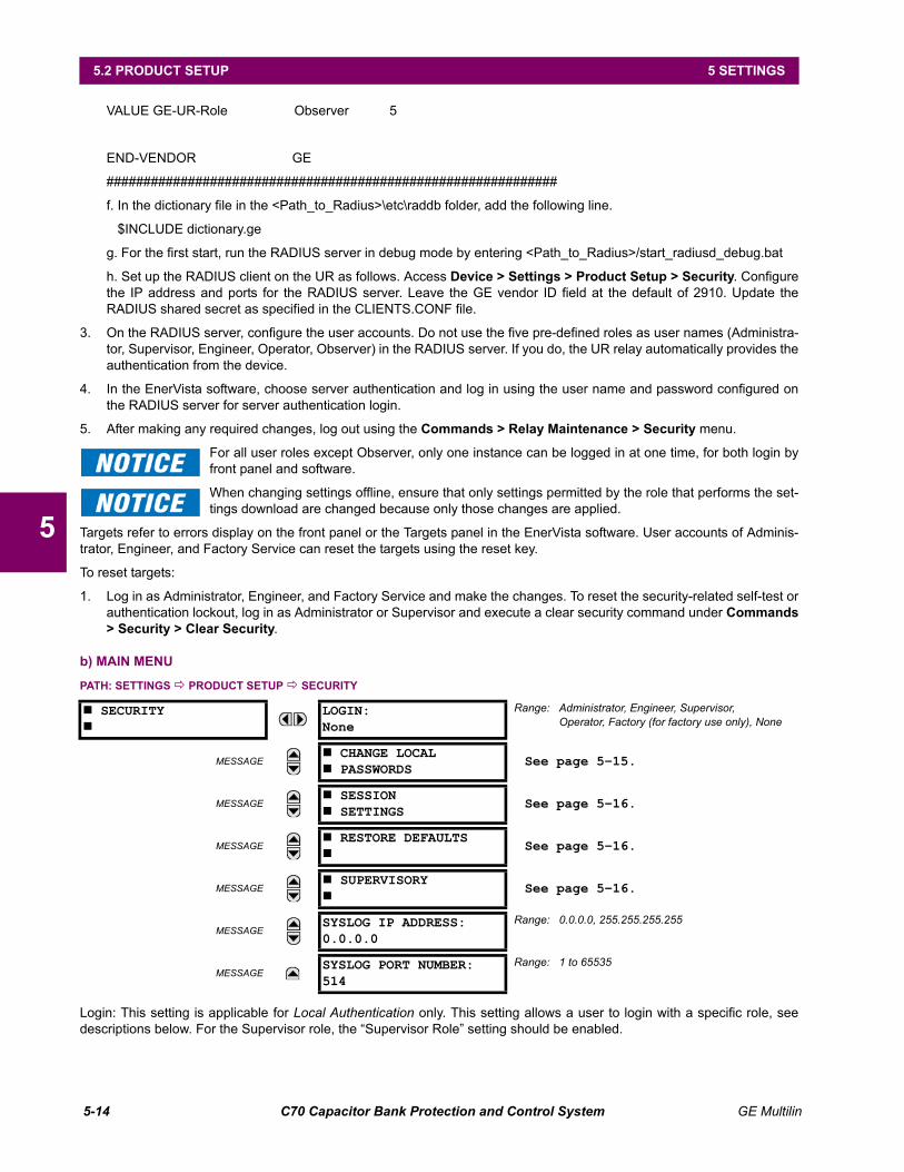
5-14 C70 Capacitor Bank Protection and Control System GE Multilin
5.2 PRODUCT SETUP 5 SETTINGS
5
VALUE GE-UR-Role Observer 5
END-VENDOR GE
#############################################################
f. In the dictionary file in the <Path_to_Radius>\etc\raddb folder, add the following line.
$INCLUDE dictionary.ge
g. For the first start, run the RADIUS server in debug mode by entering <Path_to_Radius>/start_radiusd_debug.bat
h. Set up the RADIUS client on the UR as follows. Access Device > Settings > Product Setup > Security. Configurethe IP address and ports for the RADIUS server. Leave the GE vendor ID field at the default of 2910. Update theRADIUS shared secret as specified in the CLIENTS.CONF file.
3. On the RADIUS server, configure the user accounts. Do not use the five pre-defined roles as user names (Administra-tor, Supervisor, Engineer, Operator, Observer) in the RADIUS server. If you do, the UR relay automatically provides theauthentication from the device.
4. In the EnerVista software, choose server authentication and log in using the user name and password configured onthe RADIUS server for server authentication login.
5. After making any required changes, log out using the Commands > Relay Maintenance > Security menu.
For all user roles except Observer, only one instance can be logged in at one time, for both login byfront panel and software.
When changing settings offline, ensure that only settings permitted by the role that performs the set-tings download are changed because only those changes are applied.
Targets refer to errors display on the front panel or the Targets panel in the EnerVista software. User accounts of Adminis-trator, Engineer, and Factory Service can reset the targets using the reset key.
To reset targets:
1. Log in as Administrator, Engineer, and Factory Service and make the changes. To reset the security-related self-test orauthentication lockout, log in as Administrator or Supervisor and execute a clear security command under Commands> Security > Clear Security.
b) MAIN MENU
PATH: SETTINGS PRODUCT SETUP SECURITY
Login: This setting is applicable for Local Authentication only. This setting allows a user to login with a specific role, seedescriptions below. For the Supervisor role, the “Supervisor Role” setting should be enabled.
SECURITY
LOGIN:None
Range: Administrator, Engineer, Supervisor,Operator, Factory (for factory use only), None
MESSAGE CHANGE LOCAL PASSWORDS
See page 5–15.
MESSAGE SESSION SETTINGS
See page 5–16.
MESSAGE RESTORE DEFAULTS
See page 5–16.
MESSAGE SUPERVISORY
See page 5–16.
MESSAGESYSLOG IP ADDRESS:0.0.0.0
Range: 0.0.0.0, 255.255.255.255
MESSAGESYSLOG PORT NUMBER:514
Range: 1 to 65535

GE Multilin C70 Capacitor Bank Protection and Control System 5-15
5 SETTINGS 5.2 PRODUCT SETUP
5
Whenever a new role is logged in, the user is prompted with a display to enter a password. 20 alphanumeric characters areacceptable as passwords.The UR device supports five roles. All roles have their corresponding passwords. The Observerrole is the only role that does not require a password.
The roles are defined as follows:
• Administrator: Complete read and write access to all settings and commands. This role does not allow concurrentaccess. This role has an operand to indicate when it is logged on.
• Engineer: Complete read and write access to all settings and commands with the exception of configuring Security set-tings and Firmware upgrades. This role does not allow concurrent access.
• Operator: The Operator has read/write access to all settings under the command menu/section. This role does notexist offline.
• Supervisor: This is only an approving role. This role’s authentication commits setting changes submitted by Administra-tor or Engineer. The Supervisor role authenticates to unlock the UR relay for setting changes and not approve changesafter the fact. Only Supervisor can set the Settings and Firmware Lock in the Security Settings. This role also has theability to forcefully logoff any other role and clear the security event log. This role can also be disabled, but onlythrough a Supervisor authentication. When this role is disabled its permissions are assigned to the Administrator role.
• Observer: This role has read only access to all UR settings. This role allows unlimited concurrent access but it has nodownload access to any files on the device. Observer is the default role if no authentication has been done to thedevice. This role displays as "None" on the front panel.
The Factory service role is not available and is intended for factory use only.
c) LOCAL PASSWORDS
PATH: SETTINGS PRODUCT SETUP SECURITY CHANGE LOCAL PASSWORDS
The Change Local Passwords menu is shown on the front panel and Enervista on a successful login of Administrator role.
The “login setting” in this menu is similar to the login setting described in PATH: SETTINGS > PRODUCT SETUP > SECU-RITY except for the factory role.
Passwords are stored in text format. No encryption is applied.
Notes:
• In Local Authentication mode, the Observer role does not have a password associated with it. In Remote Authentica-tion mode the Observer role requires a password.
• The default password is “ChangeMe1#”.
• Once the passwords are set, the Administrator with Supervisor approval can change the role associated password.
• In CyberSentry, password encryption is not supported.
CHANGE LOCAL PASSWORDS
LOGIN:None
Range: 20 Alphanumeric Characters
MESSAGENEW PASSWORD: Range: 20 Alphanumeric Characters
MESSAGECONFIRM PASSWORD: Range: 20 Alphanumeric Characters
NOTE
NOTE

5-16 C70 Capacitor Bank Protection and Control System GE Multilin
5.2 PRODUCT SETUP 5 SETTINGS
5
d) SESSION SETTINGS
PATH: SETTINGS PRODUCT SETUP SECURITY SESSION SETTINGS
The following session settings are available.
• SESSION LOCKOUT: This setting specifies the number of failed authentications (the default is three and the maxi-mum is 99) before the device blocks subsequent authentication attempts for the lockout period. A value of zero meanslockout is disabled.
• SESSION LOCKOUT PERIOD: This setting specifies the period of time in minutes of a lockout period (the default isthree and the maximum is 9999). A value of 0 means that there is no lockout period.
e) RESTORE DEFAULTS
PATH: SETTINGS PRODUCT SETUP SECURITY RESTORE DEFAULTS
• LOAD FACTORY DEFAULTS: This setting is used to reset all the settings, communication and security passwords. AnAdministrator role is used to change this setting and a Supervisor role (if not disabled) approves it.
f) SUPERVISORY
PATH: SETTINGS PRODUCT SETUP SECURITY SUPERVISORY
SESSION SETTINGS
SESSION LOCKOUT: 3
Range: 0 to 99
MESSAGESESSION LOCKOUTPERIOD: 3 min
Range: 0 to 9999 minutes
RESTORE DEFAULTS
LOAD FACTORYDEFAULTS: No
Range: Yes, No
SUPERVISORY
LOCAL AUTHENTICATION:Yes
Range: Yes, No
MESSAGEBYPASS ACCESS:Disabled
Range: Enabled, Disabled
MESSAGELOCK RELAY:Disabled
Range: Enabled, Disabled
MESSAGEFACTORY SERVICE:MODE: Disabled
Range: Enabled, Disabled
MESSAGE SELF TESTS
See below
MESSAGESUPERVISOR ROLE:Disabled
Range: Enabled, Disabled
MESSAGESERIAL INACTIVITYTIMEOUT: 1 min
Range: 1 to 9999 minutes

GE Multilin C70 Capacitor Bank Protection and Control System 5-17
5 SETTINGS 5.2 PRODUCT SETUP
5
The Supervisory menu settings are available for Supervisor role only or if the Supervisor role is disabled then for theAdministrator role only.
Figure 5–2: SUPERVISORY PANEL
Local Authentication: This setting is enabled by default, meaning "Yes" is selected. When enabled, Device Authenticationwith roles is enabled. When this setting is disabled, the UR only authenticates to the AAA server (Radius). However, theAdministrator and Supervisor (when enabled) remain active even after device authentication is disabled and their only per-mission is to re-enable device authentication. To re-enable device authentication, the Supervisor unlocks the device for set-ting changes, then the Administrator re-enables device authentication.
Bypass Access: Enabling this setting allows 502 Ethernet sessions to the relay. The serial ports (RS232 and RS485) allowsettings write. No passwords or roles are required when in this mode. When disabled, everything goes back to normal. Thissetting has no effect on the front panel and it continues to support Role Based Access Control (RBAC).
Lock Relay: This setting uses a Boolean value (Enable/Disable) to indicate if the device accepts setting changes andwhether the device can receive a firmware upgrade. This setting can be changed only by the Supervisor role, if it is enabledor by the Administrator if the Supervisor role is disabled. The Supervisor role enables this setting for the relay to startaccepting setting changes or command changes or firmware upgrade. After all the setting changes are applied or com-mands executed, the Supervisor disables to lock setting changes.
Example: If this setting is "Yes" and an attempt is made to change settings or upgrade the firmware, the UR device deniesthe setting changes and denies upgrading the firmware. If this setting is "No", the UR device accepts setting changes andfirmware upgrade.
This role is disabled by default.
MODE SERIAL (RS232 & RS485) 502 ETHERNET SSH ETHERNET
Bypass Access = Disabled Local Authenticationand Role Based Access Control (RBAC)and passwords in clear
Read only Local/Remote Authenticationand Role Based Access Control (RBAC)and passwords encrypted
Bypass Access = Enabled No Role Based Access Control (RBAC)and no passwords
No Role Based Access Control (RBAC)and no passwords
Local/Remote Authenticationand Role Based Access Control (RBAC)and passwords encrypted

5-18 C70 Capacitor Bank Protection and Control System GE Multilin
5.2 PRODUCT SETUP 5 SETTINGS
5
Supervisor Role: When enabled (i.e., "Yes" is selected) the Supervisor role is active. When "No" is selected this role is dis-abled. To disabled this setting a Supervisor authentication is necessary. If disabled, the Supervisor role is not allowed to logon. In this case the Administrator can change the settings under the Supervisory menu.
If enabled, Supervisor authentication is required to change the settings in the Supervisory menu. If the Supervisor disableshis role after authentication, the Supervisor session remains valid until he switches to another role using MMI or until heends the current Supervisor session if using communications.
This role is disabled by default.
Factory Service Mode: When enabled (i.e., "Yes" is selected) the device can go into factory service mode. For this set-ting to become enabled a Supervisor authentication is necessary. The default value is Disable.
Serial Inactivity Timeout: The role logged via a serial port is auto logged off after the Serial Inactivity timer times out. Aseparate timer is maintained for RS232 and RS485 connections. The default value is 1 minute.
SELF TESTS
PATH: SETTINGS PRODUCT SETUP SECURITY SUPERVISORY SELF TESTS
Failed Authentications: If this setting is Enabled then the number of failed authentications is compared with the Sessionlockout threshold. When the Session lockout threshold is exceeded, this minor alarm indication comes up.
Firmware Lock: If this setting is Enabled then any firmware upgrade operation attempt when the “LOCK FIRMWAREUPGRADE” setting is set to “Yes” brings up this self test alarm.
Settings Lock: If this setting is Enabled then an unauthorized write attempt to a setting for a given role activates this selftest.
PATH: SETTINGS PRODUCT SETUP SECURITY SUPERVISORY SELF TESTS FAILED AUTHENTICATE
SELF TESTS
FAILED AUTHENTICATE
See below
MESSAGEFIRMWARE LOCK:Enabled
Range: Enabled, Disabled
MESSAGESETTINGS LOCK:Enabled
Range: Enabled, Disabled
FAILED AUTHENTICATE
FAILED AUTHENTICATE:Enabled
Range: Enabled, Disabled

GE Multilin C70 Capacitor Bank Protection and Control System 5-19
5 SETTINGS 5.2 PRODUCT SETUP
5
5.2.3 DISPLAY PROPERTIES
PATH: SETTINGS PRODUCT SETUP DISPLAY PROPERTIES
Some relay messaging characteristics can be modified to suit different situations using the display properties settings.
• LANGUAGE: This setting selects the language used to display settings, actual values, and targets. The range isdependent on the order code of the relay.
• FLASH MESSAGE TIME: Flash messages are status, warning, error, or information messages displayed for severalseconds in response to certain key presses during setting programming. These messages override any normal mes-sages. The duration of a flash message on the display can be changed to accommodate different reading rates.
• DEFAULT MESSAGE TIMEOUT: If the keypad is inactive for a period of time, the relay automatically reverts to adefault message. The inactivity time is modified via this setting to ensure messages remain on the screen long enoughduring programming or reading of actual values.
• DEFAULT MESSAGE INTENSITY: To extend phosphor life in the vacuum fluorescent display, the brightness can beattenuated during default message display. During keypad interrogation, the display always operates at full brightness.
• SCREEN SAVER FEATURE and SCREEN SAVER WAIT TIME: These settings are only visible if the C70 has a liquidcrystal display (LCD) and control its backlighting. When the SCREEN SAVER FEATURE is “Enabled”, the LCD backlightingis turned off after the DEFAULT MESSAGE TIMEOUT followed by the SCREEN SAVER WAIT TIME, providing that no keyshave been pressed and no target messages are active. When a keypress occurs or a target becomes active, the LCDbacklighting is turned on.
• CURRENT CUT-OFF LEVEL: This setting modifies the current cut-off threshold. Very low currents (1 to 2% of therated value) are very susceptible to noise. Some customers prefer very low currents to display as zero, while othersprefer the current be displayed even when the value reflects noise rather than the actual signal. The C70 applies a cut-off value to the magnitudes and angles of the measured currents. If the magnitude is below the cut-off level, it is substi-tuted with zero. This applies to phase and ground current phasors as well as true RMS values and symmetrical compo-nents. The cut-off operation applies to quantities used for metering, protection, and control, as well as those used bycommunications protocols. Note that the cut-off level for the sensitive ground input is 10 times lower that the CURRENT
CUT-OFF LEVEL setting value. Raw current samples available via oscillography are not subject to cut-off.
• VOLTAGE CUT-OFF LEVEL: This setting modifies the voltage cut-off threshold. Very low secondary voltage measure-ments (at the fractional volt level) can be affected by noise. Some customers prefer these low voltages to be displayedas zero, while others prefer the voltage to be displayed even when the value reflects noise rather than the actual sig-nal. The C70 applies a cut-off value to the magnitudes and angles of the measured voltages. If the magnitude is belowthe cut-off level, it is substituted with zero. This operation applies to phase and auxiliary voltages, and symmetrical
DISPLAY PROPERTIES
LANGUAGE:English
Range: English; English, French; English, Russian;English, Chinese(range dependent on order code)
MESSAGEFLASH MESSAGETIME: 1.0 s
Range: 0.5 to 10.0 s in steps of 0.1
MESSAGEDEFAULT MESSAGETIMEOUT: 300 s
Range: 10 to 900 s in steps of 1
MESSAGEDEFAULT MESSAGEINTENSITY: 25 %
Range: 25%, 50%, 75%, 100%Visible only if a VFD is installed
MESSAGESCREEN SAVERFEATURE: Disabled
Range: Disabled, EnabledVisible only if an LCD is installed
MESSAGESCREEN SAVER WAITTIME: 30 min
Range: 1 to 65535 min. in steps of 1Visible only if an LCD is installed
MESSAGECURRENT CUT-OFFLEVEL: 0.020 pu
Range: 0.002 to 0.020 pu in steps of 0.001
MESSAGEVOLTAGE CUT-OFFLEVEL: 1.0 V
Range: 0.1 to 1.0 V secondary in steps of 0.1

5-20 C70 Capacitor Bank Protection and Control System GE Multilin
5.2 PRODUCT SETUP 5 SETTINGS
5
components. The cut-off operation applies to quantities used for metering, protection, and control, as well as thoseused by communications protocols. Raw samples of the voltages available via oscillography are not subject cut-off.
The CURRENT CUT-OFF LEVEL and the VOLTAGE CUT-OFF LEVEL are used to determine the metered power cut-off levels. Thepower cut-off level is calculated as shown below. For Delta connections:
(EQ 5.3)
For Wye connections:
(EQ 5.4)
(EQ 5.5)
where VT primary = VT secondary VT ratio and CT primary = CT secondary CT ratio.
For example, given the following settings:
CURRENT CUT-OFF LEVEL: “0.02 pu”VOLTAGE CUT-OFF LEVEL: “1.0 V”PHASE CT PRIMARY: “100 A”PHASE VT SECONDARY: “66.4 V”PHASE VT RATIO: “208.00 : 1"PHASE VT CONNECTION: “Delta”.
We have:
CT primary = “100 A”, andVT primary = PHASE VT SECONDARY x PHASE VT RATIO = 66.4 V x 208 = 13811.2 V
The power cut-off is therefore:
power cut-off = (CURRENT CUT-OFF LEVEL VOLTAGE CUT-OFF LEVEL CT primary VT primary)/VT secondary= ( 0.02 pu 1.0 V 100 A 13811.2 V) / 66.4 V = 720.5 watts
Any calculated power value below this cut-off will not be displayed. As well, the three-phase energy data will not accumu-late if the total power from all three phases does not exceed the power cut-off.
Lower the VOLTAGE CUT-OFF LEVEL and CURRENT CUT-OFF LEVEL with care as the relay accepts lower signalsas valid measurements. Unless dictated otherwise by a specific application, the default settings of “0.02pu” for CURRENT CUT-OFF LEVEL and “1.0 V” for VOLTAGE CUT-OFF LEVEL are recommended.
5.2.4 CLEAR RELAY RECORDS
PATH: SETTINGS PRODUCT SETUP CLEAR RELAY RECORDS
CLEAR RELAY RECORDS
CLEAR USER REPORTS:Off
Range: FlexLogic operand
MESSAGECLEAR EVENT RECORDS:Off
Range: FlexLogic operand
MESSAGECLEAR OSCILLOGRAPHY?No
Range: FlexLogic operand
MESSAGECLEAR DATA LOGGER:Off
Range: FlexLogic operand
MESSAGERESET UNAUTH ACCESS:Off
Range: FlexLogic operand
MESSAGECLEAR DIR I/O STATS:Off
Range: FlexLogic operand.Valid only for units with Direct I/O module.
3-phase power cut-off 3 CURRENT CUT-OFF LEVEL VOLTAGE CUT-OFF LEVEL VT primary CT primaryVT secondary
------------------------------------------------------------------------------------------------------------------------------------------------------------------------------------------------------------------------------=
3-phase power cut-off 3 CURRENT CUT-OFF LEVEL VOLTAGE CUT-OFF LEVEL VT primary CT primaryVT secondary
--------------------------------------------------------------------------------------------------------------------------------------------------------------------------------------------------------------------------=
per-phase power cut-off CURRENT CUT-OFF LEVEL VOLTAGE CUT-OFF LEVEL VT primary CT primaryVT secondary
----------------------------------------------------------------------------------------------------------------------------------------------------------------------------------------------------------------=
3
NOTE
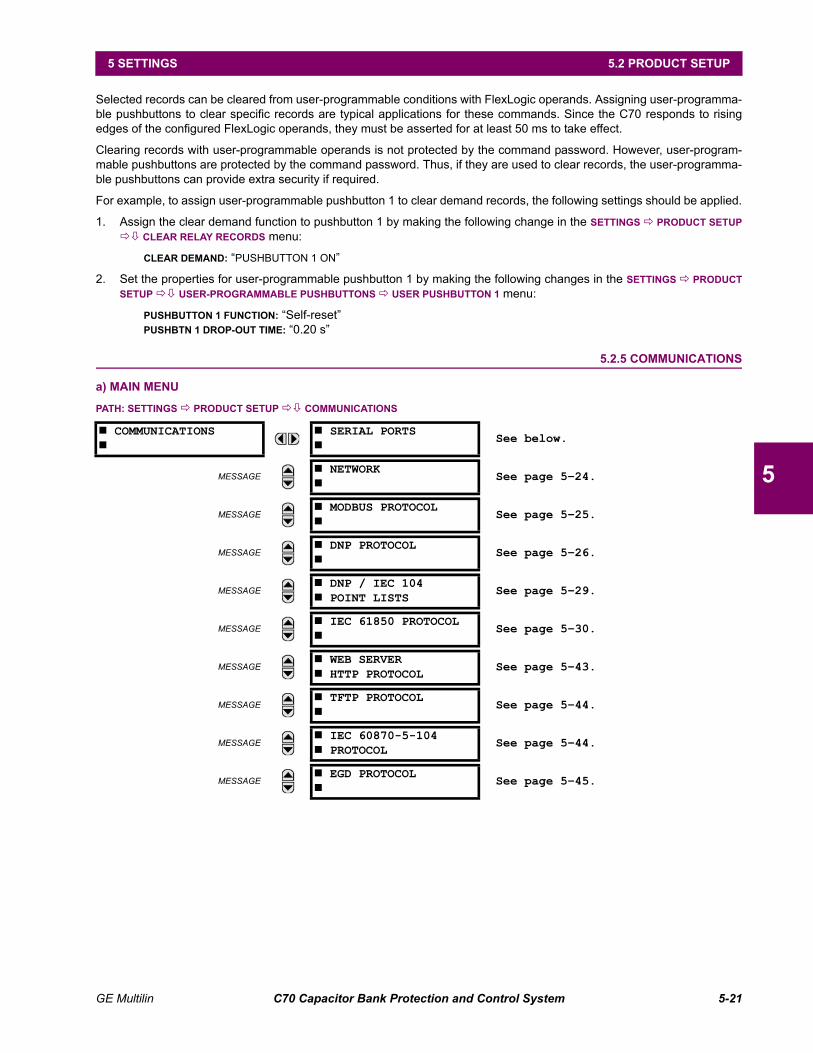
GE Multilin C70 Capacitor Bank Protection and Control System 5-21
5 SETTINGS 5.2 PRODUCT SETUP
5
Selected records can be cleared from user-programmable conditions with FlexLogic operands. Assigning user-programma-ble pushbuttons to clear specific records are typical applications for these commands. Since the C70 responds to risingedges of the configured FlexLogic operands, they must be asserted for at least 50 ms to take effect.
Clearing records with user-programmable operands is not protected by the command password. However, user-program-mable pushbuttons are protected by the command password. Thus, if they are used to clear records, the user-programma-ble pushbuttons can provide extra security if required.
For example, to assign user-programmable pushbutton 1 to clear demand records, the following settings should be applied.
1. Assign the clear demand function to pushbutton 1 by making the following change in the SETTINGS PRODUCT SETUP
CLEAR RELAY RECORDS menu:
CLEAR DEMAND: “PUSHBUTTON 1 ON”
2. Set the properties for user-programmable pushbutton 1 by making the following changes in the SETTINGS PRODUCT
SETUP USER-PROGRAMMABLE PUSHBUTTONS USER PUSHBUTTON 1 menu:
PUSHBUTTON 1 FUNCTION: “Self-reset”PUSHBTN 1 DROP-OUT TIME: “0.20 s”
5.2.5 COMMUNICATIONS
a) MAIN MENU
PATH: SETTINGS PRODUCT SETUP COMMUNICATIONS
COMMUNICATIONS
SERIAL PORTS
See below.
MESSAGE NETWORK
See page 5–24.
MESSAGE MODBUS PROTOCOL
See page 5–25.
MESSAGE DNP PROTOCOL
See page 5–26.
MESSAGE DNP / IEC 104 POINT LISTS
See page 5–29.
MESSAGE IEC 61850 PROTOCOL
See page 5–30.
MESSAGE WEB SERVER HTTP PROTOCOL
See page 5–43.
MESSAGE TFTP PROTOCOL
See page 5–44.
MESSAGE IEC 60870-5-104 PROTOCOL
See page 5–44.
MESSAGE EGD PROTOCOL
See page 5–45.

5-22 C70 Capacitor Bank Protection and Control System GE Multilin
5.2 PRODUCT SETUP 5 SETTINGS
5
b) SERIAL PORTS
PATH: SETTINGS PRODUCT SETUP COMMUNICATIONS SERIAL PORTS
The C70 is equipped with up to two independent serial communication ports. The faceplate RS232 port is intended for localuse and is fixed at 19200 baud and no parity. The rear COM2 port is RS485. The RS485 port has settings for baud rate andparity. It is important that these parameters agree with the settings used on the computer or other equipment that is con-nected to these ports. Any of these ports can be connected to a computer running EnerVista UR Setup. This software candownload and upload setting files, view measured parameters, and upgrade the relay firmware. A maximum of 32 relayscan be daisy-chained and connected to a DCS, PLC, or computer using the RS485 ports.
For the RS485 port, the minimum time before the port transmits after receiving data from a host can be set. Thisfeature allows operation with hosts which hold the RS485 transmitter active for some time after each transmission.
c) ETHERNET NETWORK TOPOLOGY
The three independent UR ports do not have routing capability and work only on local subnets for the switched networktopology. End nodes can communicate with each other using all supported protocols of the UR family on a local network. Ina routed network, it is recommended to upgrade the UR device used to 7.1x or higher where routing capability throughstatic route settings has been introduced.
When using more than one Ethernet port, configure each to belong to a different network or subnet using the IP addressesand mask, else communication becomes unpredictable when more than one port is configured to the same subnet.
Example 1
IP1/Mask1: 10.1.1.2/255.255.255.0 (where LAN 1 is 10.1.1.x/255.255.255.0)
IP2/Mask2: 10.2.1.2/255.255.255.0 (where LAN2 is 10.2.1.x/255.255.255.0)
IP3/Mask3: 10.3.1.2/255.255.255.0 (where LAN3 is 10.3.1.x/255.255.255.0)
Example 2
IP1/Mask1: 10.1.1.2/255.0.0.0 (where LAN1 is 10.x.x.x/255.0.0.0)
IP2/Mask2: 11.1.1.2/255.0.0.0 (where LAN2 is 11.x.x.x/255.0.0.0)
IP3/Mask3: 12.1.1.2/255.0.0.0 (where LAN3 is 12.x.x.x/255.0.0.0)
Example 3 — Incorrect
IP1/Mask1: 10.1.1.2/255.0.0.0
IP2/Mask2: 10.2.1.2/255.0.0.0
IP3/Mask3: 10.3.1.2/255.0.0.0
This example is incorrect because the mask of 255.0.0.0 used for the three IP addresses makes them belong to the samenetwork of 10.x.x.x.
SERIAL PORTS
RS485 COM2 BAUDRATE: 19200
Range: 300, 1200, 2400, 4800, 9600, 14400, 19200,28800, 33600, 38400, 57600, 115200
MESSAGERS485 COM2 PARITY:None
Range: None, Odd, Even
MESSAGERS485 COM2 RESPONSEMIN TIME: 0 ms
Range: 0 to 1000 ms in steps of 10
NOTE
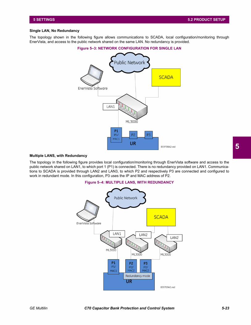
GE Multilin C70 Capacitor Bank Protection and Control System 5-23
5 SETTINGS 5.2 PRODUCT SETUP
5
Single LAN, No Redundancy
The topology shown in the following figure allows communications to SCADA, local configuration/monitoring throughEnerVista, and access to the public network shared on the same LAN. No redundancy is provided.
Figure 5–3: NETWORK CONFIGURATION FOR SINGLE LAN
Multiple LANS, with Redundancy
The topology in the following figure provides local configuration/monitoring through EnerVista software and access to thepublic network shared on LAN1, to which port 1 (P1) is connected. There is no redundancy provided on LAN1. Communica-tions to SCADA is provided through LAN2 and LAN3, to which P2 and respectively P3 are connected and configured towork in redundant mode. In this configuration, P3 uses the IP and MAC address of P2.
Figure 5–4: MULTIPLE LANS, WITH REDUNDANCY
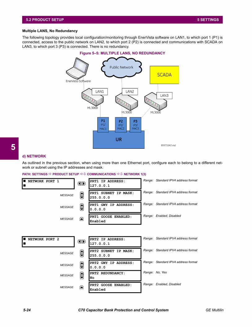
5-24 C70 Capacitor Bank Protection and Control System GE Multilin
5.2 PRODUCT SETUP 5 SETTINGS
5
Multiple LANS, No Redundancy
The following topology provides local configuration/monitoring through EnerVista software on LAN1, to which port 1 (P1) isconnected, access to the public network on LAN2, to which port 2 (P2) is connected and communications with SCADA onLAN3, to which port 3 (P3) is connected. There is no redundancy.
Figure 5–5: MULTIPLE LANS, NO REDUNDANCY
d) NETWORK
As outlined in the previous section, when using more than one Ethernet port, configure each to belong to a different net-work or subnet using the IP addresses and mask.
PATH: SETTINGS PRODUCT SETUP COMMUNICATIONS NETWORK 1(3)
NETWORK PORT 1
PRT1 IP ADDRESS:127.0.0.1
Range: Standard IPV4 address format
MESSAGEPRT1 SUBNET IP MASK:255.0.0.0
Range: Standard IPV4 address format
MESSAGEPRT1 GWY IP ADDRESS:0.0.0.0
Range: Standard IPV4 address format
MESSAGEPRT1 GOOSE ENABLED:Enabled
Range: Enabled, Disabled
NETWORK PORT 2
PRT2 IP ADDRESS:127.0.0.1
Range: Standard IPV4 address format
MESSAGEPRT2 SUBNET IP MASK:255.0.0.0
Range: Standard IPV4 address format
MESSAGEPRT2 GWY IP ADDRESS:0.0.0.0
Range: Standard IPV4 address format
MESSAGEPRT2 REDUNDANCY:No
Range: No, Yes
MESSAGEPRT2 GOOSE ENABLED:Enabled
Range: Enabled, Disabled

GE Multilin C70 Capacitor Bank Protection and Control System 5-25
5 SETTINGS 5.2 PRODUCT SETUP
5
The PRT1 (2, 3) GOOSE ENABLED setting provides the ability to disable/enable GOOSE transmission from the port.
PRT2 REDUNDANCY determines if ports 2 and 3 operate in redundant or independent mode. In non-redundant mode, port 2and 3 operate independently with their own MAC and IP address. In redundant mode, port 2 and 3 use the port 2 MAC andIP address, port 3 is in standby mode and monitors its link to the Multilink switch, and when port 2 detects a problem withthe link then communication switches to port 3 until the link returns.
The IP addresses are used with the DNP, Modbus/TCP, IEC 61580, IEC 60870-5-104, TFTP, and HTTP protocols. Eachnetwork protocol has a setting for the TCP/UDP port number. These settings are used only in advanced network configura-tions and should normally be left at their default values, but may be changed if required (for example, to allow access tomultiple UR-series relays behind a router). By setting a different TCP/UDP PORT NUMBER for a given protocol on each UR-series relay, the router can map the relays to the same external IP address. The client software (EnerVista UR Setup, forexample) must be configured to use the correct port number if these settings are used.
When any TCP/UDP port number or any user map setting (when used with DNP) is changed, it becomes activewhen power to the relay has been cycled (off-on).
Do not set more than one protocol to the same TCP/UDP Port Number, as this results in unreliable operation ofthose protocols.
e) MODBUS PROTOCOL
PATH: SETTINGS PRODUCT SETUP COMMUNICATIONS MODBUS PROTOCOL
The serial communication ports utilize the Modbus protocol, unless configured for DNP operation (see descriptions below).This allows the EnerVista UR Setup software to be used. The UR operates as a Modbus slave device only. When usingModbus protocol on the RS232 port, the C70 responds regardless of the MODBUS SLAVE ADDRESS programmed. For theRS485 port, each C70 must have a unique address from 1 to 254. Address 0 is the broadcast address which all Modbusslave devices listen to. Addresses do not have to be sequential, but no two devices can have the same address or conflictsresulting in errors will occur. Generally, each device added to the link should use the next higher address starting at 1. SeeAppendix B for more information on the Modbus protocol.
A value of 0 closes the port. When the Modbus port is set to 0, communicate with the relay using the front panel or serialport.
When a 0 value is involved in a change, the changes to the MODBUS TCP PORT NUMBER setting take effectwhen the C70 is restarted.
NETWORK PORT 3
PRT3 IP ADDRESS:127.0.0.1
Range: Standard IPV4 address format
MESSAGEPRT3 SUBNET IP MASK:255.0.0.0
Range: Standard IPV4 address format
MESSAGEPRT3 GWY IP ADDRESS:0.0.0.0
Range: Standard IPV4 address format
MESSAGEPRT3 GOOSE ENABLED:Enabled
Range: Enabled, Disabled
MODBUS PROTOCOL
MODBUS SLAVEADDRESS: 254
Range: 0 to 254 in steps of 1
MESSAGEMODBUS TCP PORTNUMBER: 502
Range: 0 to 65535 in steps of 1
NOTE
NOTE
NOTE

5-26 C70 Capacitor Bank Protection and Control System GE Multilin
5.2 PRODUCT SETUP 5 SETTINGS
5
f) DNP PROTOCOL
PATH: SETTINGS PRODUCT SETUP COMMUNICATIONS DNP PROTOCOL
DNP PROTOCOL
DNP CHANNELS
Range: see sub-menu below
MESSAGEDNP ADDRESS:1
Range: 0 to 65519 in steps of 1
MESSAGE DNP NETWORK CLIENT ADDRESSES
Range: see sub-menu below
MESSAGEDNP TCP/UDP PORTNUMBER: 20000
Range: 0 to 65535 in steps of 1
MESSAGEDNP UNSOL RESPONSEFUNCTION: Disabled
Range: Enabled, Disabled
MESSAGEDNP UNSOL RESPONSETIMEOUT: 5 s
Range: 0 to 60 s in steps of 1
MESSAGEDNP UNSOL RESPONSEMAX RETRIES: 10
Range: 1 to 255 in steps of 1
MESSAGEDNP UNSOL RESPONSEDEST ADDRESS: 1
Range: 0 to 65519 in steps of 1
MESSAGEDNP CURRENT SCALEFACTOR: 1
Range: 0.001, 0.01. 0.1, 1, 10, 100, 1000, 10000,100000
MESSAGEDNP VOLTAGE SCALEFACTOR: 1
Range: 0.001, 0.01. 0.1, 1, 10, 100, 1000, 10000,100000
MESSAGEDNP POWER SCALEFACTOR: 1
Range: 0.001, 0.01. 0.1, 1, 10, 100, 1000, 10000,100000
MESSAGEDNP ENERGY SCALEFACTOR: 1
Range: 0.001, 0.01. 0.1, 1, 10, 100, 1000, 10000,100000
MESSAGEDNP PF SCALEFACTOR: 1
Range: 0.001, 0.01. 0.1, 1, 10, 100, 1000, 10000,100000
MESSAGEDNP OTHER SCALEFACTOR: 1
Range: 0.001, 0.01. 0.1, 1, 10, 100, 1000, 10000,100000
MESSAGEDNP CURRENT DEFAULTDEADBAND: 30000
Range: 0 to 100000000 in steps of 1
MESSAGEDNP VOLTAGE DEFAULTDEADBAND: 30000
Range: 0 to 100000000 in steps of 1
MESSAGEDNP POWER DEFAULTDEADBAND: 30000
Range: 0 to 100000000 in steps of 1
MESSAGEDNP ENERGY DEFAULTDEADBAND: 30000
Range: 0 to 100000000 in steps of 1
MESSAGEDNP PF DEFAULTDEADBAND: 30000
Range: 0 to 100000000 in steps of 1
MESSAGEDNP OTHER DEFAULTDEADBAND: 30000
Range: 0 to 100000000 in steps of 1
MESSAGEDNP TIME SYNC IINPERIOD: 1440 min
Range: 1 to 10080 min. in steps of 1

GE Multilin C70 Capacitor Bank Protection and Control System 5-27
5 SETTINGS 5.2 PRODUCT SETUP
5
The C70 supports the Distributed Network Protocol (DNP) version 3.0. The C70 can be used as a DNP slave device con-nected to multiple DNP masters (usually an RTU or a SCADA master station). Since the C70 maintains two sets of DNPdata change buffers and connection information, two DNP masters can actively communicate with the C70 at one time.
The IEC 60870-5-104 and DNP protocols cannot be used simultaneously. When the IEC 60870-5-104 FUNCTIONsetting is set to “Enabled”, the DNP protocol is not operational. When this setting is changed it does not becomeactive until power to the relay has been cycled (off-to-on).
The DNP Channels sub-menu is shown below.
PATH: SETTINGS PRODUCT SETUP COMMUNICATIONS DNP PROTOCOL DNP CHANNELS
The DNP CHANNEL 1 PORT and DNP CHANNEL 2 PORT settings select the communications port assigned to the DNP protocolfor each channel. Once DNP is assigned to a serial port, the Modbus protocol is disabled on that port. When this setting isset to “Network - TCP”, the DNP protocol can be used over TCP/IP on channels 1 or 2. When this value is set to “Network -UDP”, the DNP protocol can be used over UDP/IP on channel 1 only. Refer to Appendix E for additional information on theDNP protocol.
Changes to the DNP CHANNEL 1 PORT and DNP CHANNEL 2 PORT settings take effect only after power hasbeen cycled to the relay.
The DNP NETWORK CLIENT ADDRESS settings can force the C70 to respond to a maximum of five specific DNP masters. Thesettings in this sub-menu are shown below.
MESSAGEDNP MESSAGE FRAGMENTSIZE: 240
Range: 30 to 2048 in steps of 1
MESSAGEDNP OBJECT 1DEFAULT VARIATION: 2
Range: 1, 2
MESSAGEDNP OBJECT 2DEFAULT VARIATION: 2
Range: 1, 2, 3
MESSAGEDNP OBJECT 20DEFAULT VARIATION: 1
Range: 1, 2, 5, 6
MESSAGEDNP OBJECT 21DEFAULT VARIATION: 1
Range: 1, 2, 9, 10
MESSAGEDNP OBJECT 22DEFAULT VARIATION: 1
Range: 1, 2, 5, 6
MESSAGEDNP OBJECT 23DEFAULT VARIATION: 2
Range: 1, 2, 5, 6
MESSAGEDNP OBJECT 30DEFAULT VARIATION: 1
Range: 1, 2, 3, 4, 5
MESSAGEDNP OBJECT 32DEFAULT VARIATION: 1
Range: 1, 2, 3, 4, 5, 7
MESSAGEDNP NUMBER OF PAIREDCONTROL POINTS: 0
Range: 0 to 32 in steps of 1
MESSAGEDNP TCP CONNECTIONTIMEOUT: 120 s
Range: 10 to 7200 s in steps of 1
DNP CHANNELS
DNP CHANNEL 1 PORT:NETWORK
Range: NONE, COM2 - RS485,FRONT PANEL - RS232, NETWORK - TCP,NETWORK - UDP
MESSAGEDNP CHANNEL 2 PORT:COM2 - RS485
Range: NONE, COM2 - RS485,FRONT PANEL - RS232, NETWORK - TCP,NETWORK - UDP
NOTE
NOTE

5-28 C70 Capacitor Bank Protection and Control System GE Multilin
5.2 PRODUCT SETUP 5 SETTINGS
5
PATH: SETTINGS PRODUCT SETUP COMMUNICATIONS DNP PROTOCOL DNP NETWORK CLIENT ADDRESSES
The DNP UNSOL RESPONSE FUNCTION should be “Disabled” for RS485 applications since there is no collision avoidancemechanism. The DNP UNSOL RESPONSE TIMEOUT sets the time the C70 waits for a DNP master to confirm an unsolicitedresponse. The DNP UNSOL RESPONSE MAX RETRIES setting determines the number of times the C70 retransmits an unsolic-ited response without receiving confirmation from the master; a value of “255” allows infinite re-tries. The DNP UNSOL
RESPONSE DEST ADDRESS is the DNP address to which all unsolicited responses are sent. The IP address to which unsolic-ited responses are sent is determined by the C70 from the current TCP connection or the most recent UDP message.
The DNP scale factor settings are numbers used to scale analog input point values. These settings group the C70 analoginput data into the following types: current, voltage, power, energy, power factor, and other. Each setting represents thescale factor for all analog input points of that type. For example, if the DNP VOLTAGE SCALE FACTOR setting is set to “1000”,all DNP analog input points that are voltages will be returned with values 1000 times smaller (for example, a value of 72000V on the C70 will be returned as 72). These settings are useful when analog input values must be adjusted to fit within cer-tain ranges in DNP masters. Note that a scale factor of 0.1 is equivalent to a multiplier of 10 (that is, the value will be 10times larger).
The DNP DEFAULT DEADBAND settings determine when to trigger unsolicited responses containing analog input data. Thesesettings group the C70 analog input data into the following types: current, voltage, power, energy, power factor, and other.Each setting represents the default deadband value for all analog input points of that type. For example, to trigger unsolic-ited responses from the C70 when any current values change by 15 A, the DNP CURRENT DEFAULT DEADBAND settingshould be set to “15”. Note that these settings are the deadband default values. DNP object 34 points can be used tochange deadband values, from the default, for each individual DNP analog input point. Whenever power is removed andre-applied to the C70, the default deadbands will be in effect.
The C70 relay does not support energy metering. As such, the DNP ENERGY SCALE FACTOR and DNP ENERGY
DEFAULT DEADBAND settings are not applicable.
The DNP TIME SYNC IIN PERIOD setting determines how often the Need Time Internal Indication (IIN) bit is set by the C70.Changing this time allows the DNP master to send time synchronization commands more or less often, as required.
The DNP MESSAGE FRAGMENT SIZE setting determines the size, in bytes, at which message fragmentation occurs. Largefragment sizes allow for more efficient throughput; smaller fragment sizes cause more application layer confirmations to benecessary which can provide for more robust data transfer over noisy communication channels.
When the DNP data points (analog inputs and/or binary inputs) are configured for Ethernet-enabled relays, checkthe “DNP Points Lists” C70 web page to view the points lists. This page can be viewed with a web browser by enter-ing the C70 IP address to access the C70 “Main Menu”, then by selecting the “Device Information Menu” > “DNPPoints Lists” menu item.
The DNP OBJECT 1 DEFAULT VARIATION to DNP OBJECT 32 DEFAULT VARIATION settings allow the user to select the DNPdefault variation number for object types 1, 2, 20, 21, 22, 23, 30, and 32. The default variation refers to the variationresponse when variation 0 is requested and/or in class 0, 1, 2, or 3 scans. Refer to the DNP implementation section inappendix E for additional details.
The DNP binary outputs typically map one-to-one to IED data points. That is, each DNP binary output controls a singlephysical or virtual control point in an IED. In the C70 relay, DNP binary outputs are mapped to virtual inputs. However, somelegacy DNP implementations use a mapping of one DNP binary output to two physical or virtual control points to supportthe concept of trip/close (for circuit breakers) or raise/lower (for tap changers) using a single control point. That is, the DNP
DNP NETWORK CLIENT ADDRESSES
CLIENT ADDRESS 1:0.0.0.0
Range: standard IP address
MESSAGECLIENT ADDRESS 2:0.0.0.0
Range: standard IP address
MESSAGECLIENT ADDRESS 3:0.0.0.0
Range: standard IP address
MESSAGECLIENT ADDRESS 4:0.0.0.0
Range: standard IP address
MESSAGECLIENT ADDRESS 5:0.0.0.0
Range: standard IP address
NOTE
NOTE
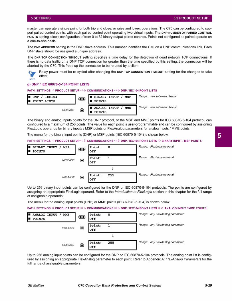
GE Multilin C70 Capacitor Bank Protection and Control System 5-29
5 SETTINGS 5.2 PRODUCT SETUP
5
master can operate a single point for both trip and close, or raise and lower, operations. The C70 can be configured to sup-port paired control points, with each paired control point operating two virtual inputs. The DNP NUMBER OF PAIRED CONTROL
POINTS setting allows configuration of from 0 to 32 binary output paired controls. Points not configured as paired operate ona one-to-one basis.
The DNP ADDRESS setting is the DNP slave address. This number identifies the C70 on a DNP communications link. EachDNP slave should be assigned a unique address.
The DNP TCP CONNECTION TIMEOUT setting specifies a time delay for the detection of dead network TCP connections. Ifthere is no data traffic on a DNP TCP connection for greater than the time specified by this setting, the connection will beaborted by the C70. This frees up the connection to be re-used by a client.
Relay power must be re-cycled after changing the DNP TCP CONNECTION TIMEOUT setting for the changes to takeeffect.
g) DNP / IEC 60870-5-104 POINT LISTS
PATH: SETTINGS PRODUCT SETUP COMMUNICATIONS DNP / IEC104 POINT LISTS
The binary and analog inputs points for the DNP protocol, or the MSP and MME points for IEC 60870-5-104 protocol, canconfigured to a maximum of 256 points. The value for each point is user-programmable and can be configured by assigningFlexLogic operands for binary inputs / MSP points or FlexAnalog parameters for analog inputs / MME points.
The menu for the binary input points (DNP) or MSP points (IEC 60870-5-104) is shown below.
PATH: SETTINGS PRODUCT SETUP COMMUNICATIONS DNP / IEC104 POINT LISTS BINARY INPUT / MSP POINTS
Up to 256 binary input points can be configured for the DNP or IEC 60870-5-104 protocols. The points are configured byassigning an appropriate FlexLogic operand. Refer to the Introduction to FlexLogic section in this chapter for the full rangeof assignable operands.
The menu for the analog input points (DNP) or MME points (IEC 60870-5-104) is shown below.
PATH: SETTINGS PRODUCT SETUP COMMUNICATIONS DNP / IEC104 POINT LISTS ANALOG INPUT / MME POINTS
Up to 256 analog input points can be configured for the DNP or IEC 60870-5-104 protocols. The analog point list is config-ured by assigning an appropriate FlexAnalog parameter to each point. Refer to Appendix A: FlexAnalog Parameters for thefull range of assignable parameters.
DNP / IEC104 POINT LISTS
BINARY INPUT / MSP POINTS
Range: see sub-menu below
MESSAGE ANALOG INPUT / MME POINTS
Range: see sub-menu below
BINARY INPUT / MSP POINTS
Point: 0Off
Range: FlexLogic operand
MESSAGEPoint: 1Off
Range: FlexLogic operand
MESSAGEPoint: 255Off
Range: FlexLogic operand
ANALOG INPUT / MME POINTS
Point: 0Off
Range: any FlexAnalog parameter
MESSAGEPoint: 1Off
Range: any FlexAnalog parameter
MESSAGEPoint: 255Off
Range: any FlexAnalog parameter
NOTE

5-30 C70 Capacitor Bank Protection and Control System GE Multilin
5.2 PRODUCT SETUP 5 SETTINGS
5
The DNP / IEC 60870-5-104 point lists always begin with point 0 and end at the first “Off” value. Since DNP / IEC60870-5-104 point lists must be in one continuous block, any points assigned after the first “Off” point are ignored.
Changes to the DNP / IEC 60870-5-104 point lists will not take effect until the C70 is restarted.
h) IEC 61850 PROTOCOL
PATH: SETTINGS PRODUCT SETUP COMMUNICATIONS IEC 61850 PROTOCOL
The C70 Capacitor Bank Protection and Control System is provided with optional IEC 61850 communica-tions capability. This feature is specified as a software option at the time of ordering. Refer to the Orderingsection of chapter 2 for additional details.
Use independent ports for IEC 61850 communication and take care when configuring the settings,else loss of protection or misoperation of the relay can result.
The C70 supports the Manufacturing Message Specification (MMS) protocol as specified by IEC 61850. MMS is supportedover two protocol stacks: TCP/IP over Ethernet. The C70 operates as an IEC 61850 server. The Remote inputs and outputssection in this chapter describe the peer-to-peer GSSE/GOOSE message scheme.
The GSSE/GOOSE configuration main menu is divided into two areas: transmission and reception.
PATH: SETTINGS PRODUCT SETUP COMMUNICATIONS IEC 61850 PROTOCOL GSSE/GOOSE CONFIGURATION
IEC 61850 PROTOCOL
GSSE / GOOSE CONFIGURATION
MESSAGE SERVER CONFIGURATION
MESSAGE IEC 61850 LOGICAL NODE NAME PREFIXES
MESSAGE MMXU DEADBANDS
MESSAGE GGIO1 STATUS CONFIGURATION
MESSAGE GGIO2 CONTROL CONFIGURATION
MESSAGE GGIO4 ANALOG CONFIGURATION
MESSAGE GGIO5 UINTEGER CONFIGURATION
MESSAGE REPORT CONTROL CONFIGURATION
MESSAGE XCBR CONFIGURATION
MESSAGE XSWI CONFIGURATION
GSSE / GOOSE CONFIGURATION
TRANSMISSION
MESSAGE RECEPTION
NOTE
NOTE

GE Multilin C70 Capacitor Bank Protection and Control System 5-31
5 SETTINGS 5.2 PRODUCT SETUP
5
The main transmission menu is shown below:
PATH: SETTINGS PRODUCT SETUP COMMUNICATIONS IEC 61850 PROTOCOL GSSE/GOOSE CONFIGURATION
TRANSMISSION
The general transmission settings are shown below:
PATH: SETTINGS PRODUCT SETUP COMMUNICATIONS IEC 61850 PROTOCOL GSSE/GOOSE CONFIGURATION
TRANSMISSION GENERAL
The DEFAULT GSSE/GOOSE UPDATE TIME sets the time between GSSE or GOOSE messages when there are no remote out-put state changes to be sent. When remote output data changes, GSSE or GOOSE messages are sent immediately. Thissetting controls the steady-state heartbeat time interval.
The DEFAULT GSSE/GOOSE UPDATE TIME setting is applicable to GSSE, fixed C70 GOOSE, and configurable GOOSE.
The GSSE settings are shown below:
PATH: SETTINGS PRODUCT SETUP COMMUNICATIONS IEC 61850 PROTOCOL GSSE/GOOSE CONFIGURATION
TRANSMISSION GSEE
These settings are applicable to GSSE only. If the fixed GOOSE function is enabled, GSSE messages are not transmitted.
The GSSE ID setting represents the IEC 61850 GSSE application ID name string sent as part of each GSSE message. Thisstring identifies the GSSE message to the receiving device. In C70 releases previous to 5.0x, this name string was repre-sented by the RELAY NAME setting.
TRANSMISSION
GENERAL
MESSAGE GSSE
MESSAGE FIXED GOOSE
MESSAGE CONFIGURABLE GOOSE
GENERAL
DEFAULT GSSE/GOOSEUPDATE TIME: 60 s
Range: 1 to 60 s in steps of 1
GSSE
GSSE FUNCTION:Enabled
Range: Enabled, Disabled
MESSAGEGSSE ID:GSSEOut
Range: 65-character ASCII string
MESSAGEDESTINATION MAC:000000000000
Range: standard MAC address

5-32 C70 Capacitor Bank Protection and Control System GE Multilin
5.2 PRODUCT SETUP 5 SETTINGS
5
The fixed GOOSE settings are shown below:
PATH: SETTINGS PRODUCT SETUP COMMUNICATIONS IEC 61850 PROTOCOL GSSE/GOOSE CONFIGURATION
TRANSMISSION FIXED GOOSE
These settings are applicable to fixed (DNA/UserSt) GOOSE only.
The GOOSE ID setting represents the IEC 61850 GOOSE application ID (GoID) name string sent as part of each GOOSEmessage. This string identifies the GOOSE message to the receiving device. In revisions previous to 5.0x, this name stringwas represented by the RELAY NAME setting.
The DESTINATION MAC setting allows the destination Ethernet MAC address to be set. This address must be a multicastaddress; the least significant bit of the first byte must be set. In C70 releases previous to 5.0x, the destination EthernetMAC address was determined automatically by taking the sending MAC address (that is, the unique, local MAC address ofthe C70) and setting the multicast bit.
The GOOSE VLAN PRIORITY setting indicates the Ethernet priority of GOOSE messages. This allows GOOSE messages tohave higher priority than other Ethernet data. The GOOSE ETYPE APPID setting allows the selection of a specific applicationID for each GOOSE sending device. This value can be left at its default if the feature is not required. Both the GOOSE VLAN
PRIORITY and GOOSE ETYPE APPID settings are required by IEC 61850.
FIXED GOOSE
GOOSE FUNCTION:Disabled
Range: Enabled, Disabled
MESSAGEGOOSE ID:GOOSEOut
Range: 65-character ASCII string
MESSAGEDESTINATION MAC:000000000000
Range: standard MAC address
MESSAGEGOOSE VLAN PRIORITY:4
Range: 0 to 7 in steps of 1
MESSAGEGOOSE VLAN ID:
0
Range: 0 to 4095 in steps of 1
MESSAGEGOOSE ETYPE APPID:
0
Range: 0 to 16383 in steps of 1

GE Multilin C70 Capacitor Bank Protection and Control System 5-33
5 SETTINGS 5.2 PRODUCT SETUP
5
The configurable GOOSE settings are shown below.
PATH: SETTINGS PRODUCT SETUP COMMUNICATIONS IEC 61850 PROTOCOL GSSE/GOOSE CONFIGURATION
TRANSMISSION CONFIGURABLE GOOSE CONFIGURABLE GOOSE 1(8)
The configurable GOOSE settings allow the C70 to be configured to transmit a number of different datasets within IEC61850 GOOSE messages. Up to eight different configurable datasets can be configured and transmitted. This is useful forintercommunication between C70 IEDs and devices from other manufacturers that support IEC 61850.
The configurable GOOSE feature allows for the configuration of the datasets to be transmitted or received from the C70.The C70 supports the configuration of eight (8) transmission and reception datasets, allowing for the optimization of datatransfer between devices.
Items programmed for dataset 1 and 2 will have changes in their status transmitted as soon as the change is detected.Datasets 1 and 2 should be used for high-speed transmission of data that is required for applications such as transfer trip-ping, blocking, and breaker fail initiate. At least one digital status value needs to be configured in the required dataset toenable transmission of configured data. Configuring analog data only to dataset 1 or 2 will not activate transmission.
Items programmed for datasets 3 through 8 will have changes in their status transmitted at a maximum rate of every100 ms. Datasets 3 through 8 will regularly analyze each data item configured within them every 100 ms to identify if anychanges have been made. If any changes in the data items are detected, these changes will be transmitted through aGOOSE message. If there are no changes detected during this 100 ms period, no GOOSE message will be sent.
For all datasets 1 through 8, the integrity GOOSE message will still continue to be sent at the pre-configured rate even if nochanges in the data items are detected.
The GOOSE functionality was enhanced to prevent the relay from flooding a communications network with GOOSE mes-sages due to an oscillation being created that is triggering a message.
The C70 has the ability of detecting if a data item in one of the GOOSE datasets is erroneously oscillating. This can becaused by events such as errors in logic programming, inputs improperly being asserted and de-asserted, or failed stationcomponents. If erroneously oscillation is detected, the C70 will stop sending GOOSE messages from the dataset for a min-imum period of one second. Should the oscillation persist after the one second time-out period, the C70 will continue toblock transmission of the dataset. The C70 will assert the MAINTENANCE ALERT: GGIO Ind XXX oscill self-test error mes-sage on the front panel display, where XXX denotes the data item detected as oscillating.
For versions 5.70 and higher, the C70 supports four retransmission schemes: aggressive, medium, relaxed, and heartbeat.The aggressive scheme is only supported in fast type 1A GOOSE messages (GOOSEOut 1 and GOOSEOut 2). For slowGOOSE messages (GOOSEOut 3 to GOOSEOut 8) the aggressive scheme is the same as the medium scheme.
CONFIGURABLE GOOSE 1
CONFIG GSE 1FUNCTION: Enabled
Range: Enabled, Disabled
MESSAGECONFIG GSE 1 ID:GOOSEOut_1
Range: 65-character ASCII string
MESSAGECONFIG GSE 1 DST MAC:000000000000
Range: standard MAC address
MESSAGECONFIG GSE 1VLAN PRIORITY: 4
Range: 0 to 7 in steps of 1
MESSAGECONFIG GSE 1VLAN ID: 0
Range: 0 to 4095 in steps of 1
MESSAGECONFIG GSE 1ETYPE APPID: 0
Range: 0 to 16383 in steps of 1
MESSAGECONFIG GSE 1CONFREV: 1
Range: 0 to 4294967295 in steps of 1
MESSAGECONFIG GSE 1 RESTRANSCURVE: Relaxed
Range: Aggressive, Medium, Relaxed, Heartbeat
MESSAGE CONFIG GSE 1 DATASET ITEMS
Range: 64 data items; each can be set to all valid MMSdata item references for transmitted data

5-34 C70 Capacitor Bank Protection and Control System GE Multilin
5.2 PRODUCT SETUP 5 SETTINGS
5
The details about each scheme are shown in the following table.
The configurable GOOSE feature is recommended for applications that require GOOSE data transfer between UR-seriesIEDs and devices from other manufacturers. Fixed GOOSE is recommended for applications that require GOOSE datatransfer between UR-series IEDs.
IEC 61850 GOOSE messaging contains a number of configurable parameters, all of which must be correct to achieve thesuccessful transfer of data. It is critical that the configured datasets at the transmission and reception devices are an exactmatch in terms of data structure, and that the GOOSE addresses and name strings match exactly. Manual configuration ispossible, but third-party substation configuration software may be used to automate the process. The EnerVista UR Setupsoftware can produce IEC 61850 ICD files and import IEC 61850 SCD files produced by a substation configurator (refer tothe IEC 61850 IED configuration section later in this appendix).
The following example illustrates the configuration required to transfer IEC 61850 data items between two devices. Thegeneral steps required for transmission configuration are:
1. Configure the transmission dataset.
2. Configure the GOOSE service settings.
3. Configure the data.
The general steps required for reception configuration are:
1. Configure the reception dataset.
2. Configure the GOOSE service settings.
3. Configure the data.
Table 5–1: GOOSE RETRANSMISSION SCHEMES
SCHEME SQ NUM TIME FROM THE EVENT
TIME BETWEEN MESSAGES
COMMENT TIME ALLOWED TO LIVE IN MESSAGE
Aggressive 0 0 ms 0 ms Event 2000 ms
1 4 ms 4 ms T1 2000 ms
2 8 ms 4 ms T1 2000 ms
3 16 ms 8 ms T2 Heartbeat * 4.5
4 Heartbeat Heartbeat T0 Heartbeat * 4.5
5 Heartbeat Heartbeat T0 Heartbeat * 4.5
Medium 0 0 ms 0 ms Event 2000 ms
1 16 ms 16 ms T1 2000 ms
2 32 ms 16 ms T1 2000 ms
3 64 ms 32 ms T2 Heartbeat * 4.5
4 Heartbeat Heartbeat T0 Heartbeat * 4.5
5 Heartbeat Heartbeat T0 Heartbeat * 4.5
Relaxed 0 0 ms 0 ms Event 2000 ms
1 100 ms 100 ms T1 2000 ms
2 200 ms 100 ms T1 2000 ms
3 700 ms 500 ms T2 Heartbeat * 4.5
4 Heartbeat Heartbeat T0 Heartbeat * 4.5
5 Heartbeat Heartbeat T0 Heartbeat * 4.5
Heartbeat 0 0 ms 0 ms Event 2000 ms
1 Heartbeat Heartbeat T1 2000 ms
2 Heartbeat Heartbeat T1 2000 ms
3 Heartbeat Heartbeat T2 Heartbeat * 4.5
4 Heartbeat Heartbeat T0 Heartbeat * 4.5
5 Heartbeat Heartbeat T0 Heartbeat * 4.5

GE Multilin C70 Capacitor Bank Protection and Control System 5-35
5 SETTINGS 5.2 PRODUCT SETUP
5
This example shows how to configure the transmission and reception of three IEC 61850 data items: a single point statusvalue, its associated quality flags, and a floating point analog value.
The following procedure illustrates the transmission configuration.
1. Configure the transmission dataset by making the following changes in the PRODUCT SETUP COMMUNICATION IEC 61850 PROTOCOL GSSE/GOOSE CONFIGURATION TRANSMISSION CONFIGURABLE GOOSE CONFIGURABLE
GOOSE 1 CONFIG GSE 1 DATASET ITEMS settings menu:
– Set ITEM 1 to “GGIO1.ST.Ind1.q” to indicate quality flags for GGIO1 status indication 1.
– Set ITEM 2 to “GGIO1.ST.Ind1.stVal” to indicate the status value for GGIO1 status indication 1.
– Set ITEM 3 to “MMXU1.MX.Hz.mag.f” to indicate the analog frequency magnitude for MMXU1 (the metered fre-quency for SRC1).
The transmission dataset now contains a quality flag, a single point status Boolean value, and a floating point analogvalue. The reception dataset on the receiving device must exactly match this structure.
2. Configure the GOOSE service settings by making the following changes in the PRODUCT SETUP COMMUNICATION
IEC 61850 PROTOCOL GSSE/GOOSE CONFIGURATION TRANSMISSION CONFIGURABLE GOOSE CONFIGU-
RABLE GOOSE 1 settings menu:
– Set CONFIG GSE 1 FUNCTION to “Enabled”.
– Set CONFIG GSE 1 ID to an appropriate descriptive string (the default value is “GOOSEOut_1”).
– Set CONFIG GSE 1 DST MAC to a multicast address (for example, 01 00 00 12 34 56).
– Set the CONFIG GSE 1 VLAN PRIORITY; the default value of “4” is OK for this example.
– Set the CONFIG GSE 1 VLAN ID value; the default value is “0”, but some switches may require this value to be “1”.
– Set the CONFIG GSE 1 ETYPE APPID value. This setting represents the ETHERTYPE application ID and must matchthe configuration on the receiver (the default value is “0”).
– Set the CONFIG GSE 1 CONFREV value. This value changes automatically as described in IEC 61850 part 7-2. Forthis example it can be left at its default value.
3. Configure the data by making the following changes in the PRODUCT SETUP COMMUNICATION IEC 61850 PROTO-
COL GGIO1 STATUS CONFIGURATION settings menu:
– Set GGIO1 INDICATION 1 to a FlexLogic operand used to provide the status of GGIO1.ST.Ind1.stVal (for example, acontact input, virtual input, a protection element status, etc.).
4. Configure the MMXU1 Hz Deadband by making the following changes in the PRODUCT SETUP COMMUNICATION IEC 61850 PROTOCOL MMXU DEADBANDS MMXU1 DEADBANDS settings menu:
– Set MMXU1 HZ DEADBAND to “0.050%”. This will result in an update to the MMXU1.MX.mag.f analog value with achange greater than 45 mHz, from the previous MMXU1.MX.mag.f value, in the source frequency.
The C70 must be rebooted (control power removed and re-applied) before these settings take effect.
The following procedure illustrates the reception configuration.
1. Configure the reception dataset by making the following changes in the PRODUCT SETUP COMMUNICATION IEC
61850 PROTOCOL GSSE/GOOSE CONFIGURATION RECEPTION CONFIGURABLE GOOSE CONFIGURABLE GOOSE
1 CONFIG GSE 1 DATASET ITEMS settings menu:
– Set ITEM 1 to “GGIO3.ST.Ind1.q” to indicate quality flags for GGIO3 status indication 1.
– Set ITEM 2 to “GGIO3.ST.Ind1.stVal” to indicate the status value for GGIO3 status indication 1.
– Set ITEM 3 to “GGIO3.MX.AnIn1.mag.f” to indicate the analog magnitude for GGIO3 analog input 1.
The reception dataset now contains a quality flag, a single point status Boolean value, and a floating point analogvalue. This matches the transmission dataset configuration above.
2. Configure the GOOSE service settings by making the following changes in the INPUTS/OUTPUTS REMOTE DEVICES
REMOTE DEVICE 1 settings menu:
– Set REMOTE DEVICE 1 ID to match the GOOSE ID string for the transmitting device. Enter “GOOSEOut_1”.
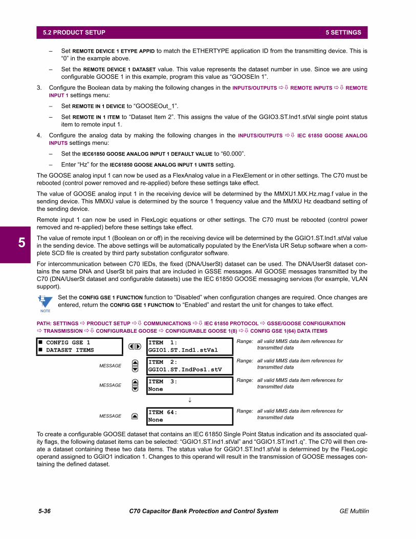
5-36 C70 Capacitor Bank Protection and Control System GE Multilin
5.2 PRODUCT SETUP 5 SETTINGS
5
– Set REMOTE DEVICE 1 ETYPE APPID to match the ETHERTYPE application ID from the transmitting device. This is“0” in the example above.
– Set the REMOTE DEVICE 1 DATASET value. This value represents the dataset number in use. Since we are usingconfigurable GOOSE 1 in this example, program this value as “GOOSEIn 1”.
3. Configure the Boolean data by making the following changes in the INPUTS/OUTPUTS REMOTE INPUTS REMOTE
INPUT 1 settings menu:
– Set REMOTE IN 1 DEVICE to “GOOSEOut_1”.
– Set REMOTE IN 1 ITEM to “Dataset Item 2”. This assigns the value of the GGIO3.ST.Ind1.stVal single point statusitem to remote input 1.
4. Configure the analog data by making the following changes in the INPUTS/OUTPUTS IEC 61850 GOOSE ANALOG
INPUTS settings menu:
– Set the IEC61850 GOOSE ANALOG INPUT 1 DEFAULT VALUE to “60.000”.
– Enter “Hz” for the IEC61850 GOOSE ANALOG INPUT 1 UNITS setting.
The GOOSE analog input 1 can now be used as a FlexAnalog value in a FlexElement or in other settings. The C70 must berebooted (control power removed and re-applied) before these settings take effect.
The value of GOOSE analog input 1 in the receiving device will be determined by the MMXU1.MX.Hz.mag.f value in thesending device. This MMXU value is determined by the source 1 frequency value and the MMXU Hz deadband setting ofthe sending device.
Remote input 1 can now be used in FlexLogic equations or other settings. The C70 must be rebooted (control powerremoved and re-applied) before these settings take effect.
The value of remote input 1 (Boolean on or off) in the receiving device will be determined by the GGIO1.ST.Ind1.stVal valuein the sending device. The above settings will be automatically populated by the EnerVista UR Setup software when a com-plete SCD file is created by third party substation configurator software.
For intercommunication between C70 IEDs, the fixed (DNA/UserSt) dataset can be used. The DNA/UserSt dataset con-tains the same DNA and UserSt bit pairs that are included in GSSE messages. All GOOSE messages transmitted by theC70 (DNA/UserSt dataset and configurable datasets) use the IEC 61850 GOOSE messaging services (for example, VLANsupport).
Set the CONFIG GSE 1 FUNCTION function to “Disabled” when configuration changes are required. Once changes areentered, return the CONFIG GSE 1 FUNCTION to “Enabled” and restart the unit for changes to take effect.
PATH: SETTINGS PRODUCT SETUP COMMUNICATIONS IEC 61850 PROTOCOL GSSE/GOOSE CONFIGURATION
TRANSMISSION CONFIGURABLE GOOSE CONFIGURABLE GOOSE 1(8) CONFIG GSE 1(64) DATA ITEMS
To create a configurable GOOSE dataset that contains an IEC 61850 Single Point Status indication and its associated qual-ity flags, the following dataset items can be selected: “GGIO1.ST.Ind1.stVal” and “GGIO1.ST.Ind1.q”. The C70 will then cre-ate a dataset containing these two data items. The status value for GGIO1.ST.Ind1.stVal is determined by the FlexLogicoperand assigned to GGIO1 indication 1. Changes to this operand will result in the transmission of GOOSE messages con-taining the defined dataset.
CONFIG GSE 1 DATASET ITEMS
ITEM 1:GGIO1.ST.Ind1.stVal
Range: all valid MMS data item references fortransmitted data
MESSAGEITEM 2:GGIO1.ST.IndPos1.stV
Range: all valid MMS data item references fortransmitted data
MESSAGEITEM 3:None
Range: all valid MMS data item references fortransmitted data
MESSAGEITEM 64:None
Range: all valid MMS data item references fortransmitted data
NOTE

GE Multilin C70 Capacitor Bank Protection and Control System 5-37
5 SETTINGS 5.2 PRODUCT SETUP
5
The main reception menu is applicable to configurable GOOSE only and contains the configurable GOOSE dataset itemsfor reception:
PATH: SETTINGS PRODUCT SETUP COMMUNICATIONS IEC 61850 PROTOCOL GSSE/GOOSE CONFIGURATION
RECEPTION CONFIGURABLE GOOSE CONFIGURABLE GOOSE 1(16) CONFIG GSE 1(32) DATA ITEMS
The configurable GOOSE settings allow the C70 to be configured to receive a number of different datasets within IEC61850 GOOSE messages. Up to sixteen different configurable datasets can be configured for reception. This is useful forintercommunication between C70 IEDs and devices from other manufacturers that support IEC 61850.
For intercommunication between C70 IEDs, the fixed (DNA/UserSt) dataset can be used. The DNA/UserSt dataset con-tains the same DNA and UserSt bit pairs that are included in GSSE messages.
To set up a C70 to receive a configurable GOOSE dataset that contains two IEC 61850 single point status indications, thefollowing dataset items can be selected (for example, for configurable GOOSE dataset 1): “GGIO3.ST.Ind1.stVal” and“GGIO3.ST.Ind2.stVal”. The C70 will then create a dataset containing these two data items. The Boolean status values fromthese data items can be utilized as remote input FlexLogic operands. First, the REMOTE DEVICE 1(16) DATASET setting mustbe set to contain dataset “GOOSEIn 1” (that is, the first configurable dataset). Then REMOTE IN 1(16) ITEM settings must beset to “Dataset Item 1” and “Dataset Item 2”. These remote input FlexLogic operands will then change state in accordancewith the status values of the data items in the configured dataset.
Double-point status values may be included in the GOOSE dataset. Received values are populated in theGGIO3.ST.IndPos1.stVal and higher items.
Floating point analog values originating from MMXU logical nodes may be included in GOOSE datasets. Deadband (non-instantaneous) values can be transmitted. Received values are used to populate the GGIO3.MX.AnIn1 and higher items.Received values are also available as FlexAnalog parameters (GOOSE analog In1 and up).
GGIO3.MX.AnIn1 to GGIO3.MX.AnIn32 can only be used once for all sixteen reception datasets.
CONFIG GSE 1 DATASET ITEMS
ITEM 1:GGIO3.ST.Ind1.stVal
Range: all valid MMS data item references fortransmitted data
MESSAGEITEM 2:GGIO3.ST.IndPos1.stV
Range: all valid MMS data item references fortransmitted data
MESSAGEITEM 3:None
Range: all valid MMS data item references fortransmitted data
MESSAGEITEM 32:None
Range: all valid MMS data item references fortransmitted data
NOTE
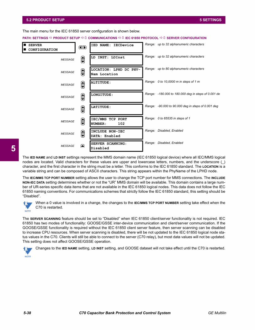
5-38 C70 Capacitor Bank Protection and Control System GE Multilin
5.2 PRODUCT SETUP 5 SETTINGS
5
The main menu for the IEC 61850 server configuration is shown below.
PATH: SETTINGS PRODUCT SETUP COMMUNICATIONS IEC 61850 PROTOCOL SERVER CONFIGURATION
The IED NAME and LD INST settings represent the MMS domain name (IEC 61850 logical device) where all IEC/MMS logicalnodes are located. Valid characters for these values are upper and lowercase letters, numbers, and the underscore (_)character, and the first character in the string must be a letter. This conforms to the IEC 61850 standard. The LOCATION is avariable string and can be composed of ASCII characters. This string appears within the PhyName of the LPHD node.
The IEC/MMS TCP PORT NUMBER setting allows the user to change the TCP port number for MMS connections. The INCLUDE
NON-IEC DATA setting determines whether or not the “UR” MMS domain will be available. This domain contains a large num-ber of UR-series specific data items that are not available in the IEC 61850 logical nodes. This data does not follow the IEC61850 naming conventions. For communications schemes that strictly follow the IEC 61850 standard, this setting should be“Disabled”.
When a 0 value is involved in a change, the changes to the IEC/MMS TCP PORT NUMBER setting take effect when theC70 is restarted.
The SERVER SCANNING feature should be set to “Disabled” when IEC 61850 client/server functionality is not required. IEC61850 has two modes of functionality: GOOSE/GSSE inter-device communication and client/server communication. If theGOOSE/GSSE functionality is required without the IEC 61850 client server feature, then server scanning can be disabledto increase CPU resources. When server scanning is disabled, there will be not updated to the IEC 61850 logical node sta-tus values in the C70. Clients will still be able to connect to the server (C70 relay), but most data values will not be updated.This setting does not affect GOOSE/GSSE operation.
Changes to the IED NAME setting, LD INST setting, and GOOSE dataset will not take effect until the C70 is restarted.
SERVER CONFIGURATION
IED NAME: IECDevice Range: up to 32 alphanumeric characters
MESSAGELD INST: LDInst Range: up to 32 alphanumeric characters
MESSAGELOCATION: LPHD DC PHV-Nam Location
Range: up to 80 alphanumeric characters
MESSAGEALTITUDE: Range: 0 to 10,0000 m in steps of 1 m
MESSAGELONGITUDE: Range: -180.000 to 180.000 deg in steps of 0.001 de
MESSAGELATITUDE: Range: -90.000 to 90.000 deg in steps of 0.001 deg
MESSAGEIEC/MMS TCP PORTNUMBER: 102
Range: 0 to 65535 in steps of 1
MESSAGEINCLUDE NON-IECDATA: Enabled
Range: Disabled, Enabled
MESSAGESERVER SCANNING:Disabled
Range: Disabled, Enabled
NOTE
NOTE
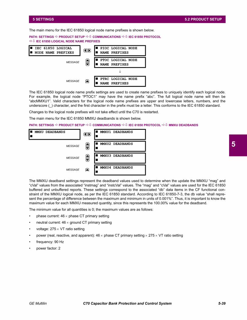
GE Multilin C70 Capacitor Bank Protection and Control System 5-39
5 SETTINGS 5.2 PRODUCT SETUP
5
The main menu for the IEC 61850 logical node name prefixes is shown below.
PATH: SETTINGS PRODUCT SETUP COMMUNICATIONS IEC 61850 PROTOCOL
IEC 61850 LOGICAL NODE NAME PREFIXES
The IEC 61850 logical node name prefix settings are used to create name prefixes to uniquely identify each logical node.For example, the logical node “PTOC1” may have the name prefix “abc”. The full logical node name will then be“abcMMXU1”. Valid characters for the logical node name prefixes are upper and lowercase letters, numbers, and theunderscore (_) character, and the first character in the prefix must be a letter. This conforms to the IEC 61850 standard.
Changes to the logical node prefixes will not take effect until the C70 is restarted.
The main menu for the IEC 61850 MMXU deadbands is shown below.
PATH: SETTINGS PRODUCT SETUP COMMUNICATIONS IEC 61850 PROTOCOL MMXU DEADBANDS
The MMXU deadband settings represent the deadband values used to determine when the update the MMXU “mag” and“cVal” values from the associated “instmag” and “instcVal” values. The “mag” and “cVal” values are used for the IEC 61850buffered and unbuffered reports. These settings correspond to the associated “db” data items in the CF functional con-straint of the MMXU logical node, as per the IEC 61850 standard. According to IEC 61850-7-3, the db value “shall repre-sent the percentage of difference between the maximum and minimum in units of 0.001%”. Thus, it is important to know themaximum value for each MMXU measured quantity, since this represents the 100.00% value for the deadband.
The minimum value for all quantities is 0; the maximum values are as follows:
• phase current: 46 phase CT primary setting
• neutral current: 46 ground CT primary setting
• voltage: 275 VT ratio setting
• power (real, reactive, and apparent): 46 phase CT primary setting 275 VT ratio setting
• frequency: 90 Hz
• power factor: 2
IEC 61850 LOGICAL NODE NAME PREFIXES
PIOC LOGICAL NODE NAME PREFIXES
MESSAGE PTOC LOGICAL NODE NAME PREFIXES
MESSAGE PTRC LOGICAL NODE NAME PREFIXES
MMXU DEADBANDS
MMXU1 DEADBANDS
MESSAGE MMXU2 DEADBANDS
MESSAGE MMXU3 DEADBANDS
MESSAGE MMXU4 DEADBANDS
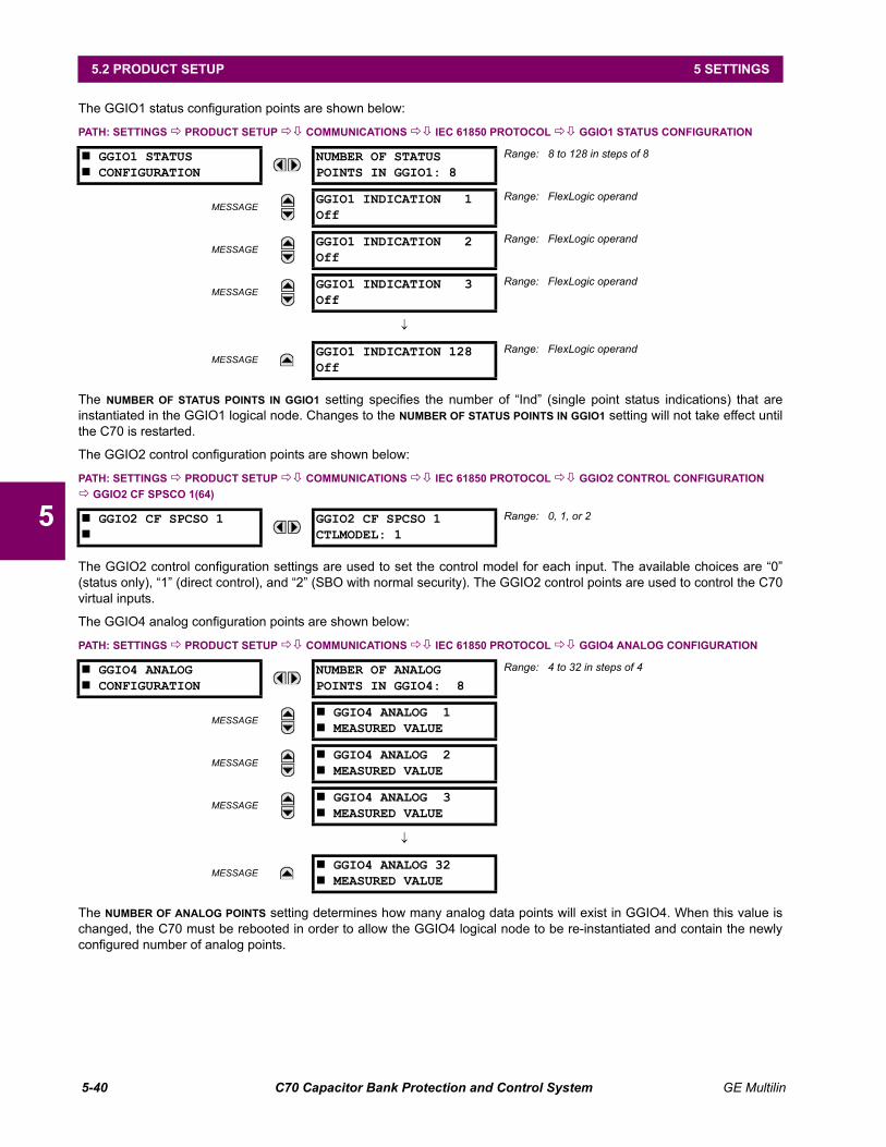
5-40 C70 Capacitor Bank Protection and Control System GE Multilin
5.2 PRODUCT SETUP 5 SETTINGS
5
The GGIO1 status configuration points are shown below:
PATH: SETTINGS PRODUCT SETUP COMMUNICATIONS IEC 61850 PROTOCOL GGIO1 STATUS CONFIGURATION
The NUMBER OF STATUS POINTS IN GGIO1 setting specifies the number of “Ind” (single point status indications) that areinstantiated in the GGIO1 logical node. Changes to the NUMBER OF STATUS POINTS IN GGIO1 setting will not take effect untilthe C70 is restarted.
The GGIO2 control configuration points are shown below:
PATH: SETTINGS PRODUCT SETUP COMMUNICATIONS IEC 61850 PROTOCOL GGIO2 CONTROL CONFIGURATION
GGIO2 CF SPSCO 1(64)
The GGIO2 control configuration settings are used to set the control model for each input. The available choices are “0”(status only), “1” (direct control), and “2” (SBO with normal security). The GGIO2 control points are used to control the C70virtual inputs.
The GGIO4 analog configuration points are shown below:
PATH: SETTINGS PRODUCT SETUP COMMUNICATIONS IEC 61850 PROTOCOL GGIO4 ANALOG CONFIGURATION
The NUMBER OF ANALOG POINTS setting determines how many analog data points will exist in GGIO4. When this value ischanged, the C70 must be rebooted in order to allow the GGIO4 logical node to be re-instantiated and contain the newlyconfigured number of analog points.
GGIO1 STATUS CONFIGURATION
NUMBER OF STATUSPOINTS IN GGIO1: 8
Range: 8 to 128 in steps of 8
MESSAGEGGIO1 INDICATION 1Off
Range: FlexLogic operand
MESSAGEGGIO1 INDICATION 2Off
Range: FlexLogic operand
MESSAGEGGIO1 INDICATION 3Off
Range: FlexLogic operand
MESSAGEGGIO1 INDICATION 128Off
Range: FlexLogic operand
GGIO2 CF SPCSO 1
GGIO2 CF SPCSO 1CTLMODEL: 1
Range: 0, 1, or 2
GGIO4 ANALOG CONFIGURATION
NUMBER OF ANALOGPOINTS IN GGIO4: 8
Range: 4 to 32 in steps of 4
MESSAGE GGIO4 ANALOG 1 MEASURED VALUE
MESSAGE GGIO4 ANALOG 2 MEASURED VALUE
MESSAGE GGIO4 ANALOG 3 MEASURED VALUE
MESSAGE GGIO4 ANALOG 32 MEASURED VALUE

GE Multilin C70 Capacitor Bank Protection and Control System 5-41
5 SETTINGS 5.2 PRODUCT SETUP
5
The measured value settings for each of the 32 analog values are shown below.
PATH: SETTINGS PRODUCT... COMMUNICATIONS IEC 61850 PROTOCOL GGIO4 ANALOG CONFIGURATION
GGIO4 ANALOG 1(32) MEASURED VALUE
These settings are configured as follows.
• ANALOG IN 1 VALUE: This setting selects the FlexAnalog value to drive the instantaneous value of each GGIO4 ana-log status value (GGIO4.MX.AnIn1.instMag.f).
• ANALOG IN 1 DB: This setting specifies the deadband for each analog value. Refer to IEC 61850-7-1 and 61850-7-3for details. The deadband is used to determine when to update the deadbanded magnitude from the instantaneousmagnitude. The deadband is a percentage of the difference between the maximum and minimum values.
• ANALOG IN 1 MIN: This setting specifies the minimum value for each analog value. Refer to IEC 61850-7-1 and61850-7-3 for details. This minimum value is used to determine the deadband. The deadband is used in the determina-tion of the deadbanded magnitude from the instantaneous magnitude.
• ANALOG IN 1 MAX: This setting defines the maximum value for each analog value. Refer to IEC 61850-7-1 and61850-7-3 for details. This maximum value is used to determine the deadband. The deadband is used in the determi-nation of the deadbanded magnitude from the instantaneous magnitude.
Note that the ANALOG IN 1 MIN and ANALOG IN 1 MAX settings are stored as IEEE 754 / IEC 60559 floating pointnumbers. Because of the large range of these settings, not all values can be stored. Some values may be roundedto the closest possible floating point number.
The GGIO5 integer configuration points are shown below:
PATH: SETTINGS PRODUCT SETUP COMMUNICATIONS IEC 61850 PROTOCOL GGIO5 ANALOG CONFIGURATION
The GGIO5 logical node allows IEC 61850 client access to integer data values. This allows access to as many as 16unsigned integer value points, associated timestamps, and quality flags. The method of configuration is similar to that ofGGIO1 (binary status values). The settings allow the selection of FlexInteger values for each GGIO5 integer value point.
It is intended that clients use GGIO5 to access generic integer values from the C70. Additional settings are provided toallow the selection of the number of integer values available in GGIO5 (1 to 16), and to assign FlexInteger values to theGGIO5 integer inputs. The following setting is available for all GGIO5 configuration points.
• GGIO5 UINT IN 1 VALUE: This setting selects the FlexInteger value to drive each GGIO5 integer status value(GGIO5.ST.UIntIn1). This setting is stored as an 32-bit unsigned integer value.
GGIO4 ANALOG 1 MEASURED VALUE
ANALOG IN 1 VALUE:Off
Range: any FlexAnalog value
MESSAGEANALOG IN 1 DB:0.000
Range: 0.000 to 100.000 in steps of 0.001
MESSAGEANALOG IN 1 MIN:0.000
Range: –1000000000.000 to 1000000000.000 in stepsof 0.001
MESSAGEANALOG IN 1 MAX:0.000
Range: –1000000000.000 to 1000000000.000 in stepsof 0.001
GGIO5 UINTEGER CONFIGURATION
GGIO5 UINT In 1:Off
Range: Off, any FlexInteger parameter
MESSAGEGGIO5 UINT In 2:Off
Range: Off, any FlexInteger parameter
MESSAGEGGIO5 UINT In 3:Off
Range: Off, any FlexInteger parameter
MESSAGEGGIO5 UINT 1n 16:Off
Range: Off, any FlexInteger parameter
NOTE

5-42 C70 Capacitor Bank Protection and Control System GE Multilin
5.2 PRODUCT SETUP 5 SETTINGS
5
The report control configuration settings are shown below:
PATH: SETTINGS PRODUCT SETUP COMMUNICATIONS IEC 61850 PROTOCOL REPORT CONTROL CONFIGURATION
CONFIGURABLE REPORT 1 REPORT 1 DATASET ITEMS
To create the dataset for logical node LN, program the ITEM 1 to ITEM 64 settings to a value from the list of IEC 61850 dataattributes supported by the C70. Changes to the dataset will only take effect when the C70 is restarted. It is recommendedto use reporting service from logical node LLN0 if a user needs some (but not all) data from already existing GGIO1,GGIO4, and MMXU4 points and their quantity is not greater than 64 minus the number items in this dataset.
The breaker configuration settings are shown below. Changes to these values will not take effect until the UR is restarted:
PATH: SETTINGS PRODUCT SETUP COMMUNICATIONS IEC 61850 PROTOCOL XCBR CONFIGURATION
The CLEAR XCBR1 OpCnt setting represents the breaker operating counter. As breakers operate by opening and closing, theXCBR operating counter status attribute (OpCnt) increments with every operation. Frequent breaker operation may resultin very large OpCnt values over time. This setting allows the OpCnt to be reset to “0” for XCBR1.
REPORT 1 DATASET ITEMS
ITEM 1: Range: all valid MMS data item references
MESSAGEITEM 2: Range: as shown above
MESSAGEITEM 3: Range: as shown above
MESSAGEITEM 64: Range: as shown above
XCBR CONFIGURATION
XCBR1 ST.LOC OPERANDOff
Range: FlexLogic operand
MESSAGEXCBR2 ST.LOC OPERANDOff
Range: FlexLogic operand
MESSAGEXCBR3 ST.LOC OPERANDOff
Range: FlexLogic operand
MESSAGEXCBR6 ST.LOC OPERANDOff
Range: FlexLogic operand
MESSAGECLEAR XCBR1 OpCnt:No
Range: No, Yes
MESSAGECLEAR XCBR2 OpCnt:No
Range: No, Yes
MESSAGECLEAR XCBR3 OpCnt:No
Range: No, Yes
MESSAGECLEAR XCBR6 OpCnt:No
Range: No, Yes

GE Multilin C70 Capacitor Bank Protection and Control System 5-43
5 SETTINGS 5.2 PRODUCT SETUP
5
The disconnect switch configuration settings are shown below. Changes to these values will not take effect until the UR isrestarted:
PATH: SETTINGS PRODUCT SETUP COMMUNICATIONS IEC 61850 PROTOCOL XSWI CONFIGURATION
The CLEAR XSWI1 OpCnt setting represents the disconnect switch operating counter. As disconnect switches operate byopening and closing, the XSWI operating counter status attribute (OpCnt) increments with every operation. Frequent switchoperation may result in very large OpCnt values over time. This setting allows the OpCnt to be reset to “0” for XSWI1.
Since GSSE/GOOSE messages are multicast Ethernet by specification, they are not usually be forwarded by net-work routers. However, GOOSE messages may be forwarded by routers if the router has been configured for VLANfunctionality.
i) WEB SERVER HTTP PROTOCOL
PATH: SETTINGS PRODUCT SETUP COMMUNICATIONS WEB SERVER HTTP PROTOCOL
The C70 contains an embedded web server and is capable of transferring web pages to a web browser such as InternetExplorer or Firefox. The web pages are organized as a series of menus that can be accessed starting at the C70 “MainMenu”. Web pages are available showing DNP and IEC 60870-5-104 points lists, Modbus registers, event records, faultreports, and so on. First connect the UR and a computer to an Ethernet network, then enter the IP address of the C70 intothe “Address” box of the web browser.
When the port is set to 0, the change takes effect when the C70 is restarted.
XSWI CONFIGURATION
XSWI1 ST.LOC OPERANDOff
Range: FlexLogic operand
MESSAGEXSWI2 ST.LOC OPERANDOff
Range: FlexLogic operand
MESSAGEXSWI3 ST.LOC OPERANDOff
Range: FlexLogic operand
MESSAGEXSWI24 ST.LOC OPERANDOff
Range: FlexLogic operand
MESSAGECLEAR XSWI1 OpCnt:No
Range: No, Yes
MESSAGECLEAR XSWI2 OpCnt:No
Range: No, Yes
MESSAGECLEAR XSWI3 OpCnt:No
Range: No, Yes
MESSAGECLEAR XSWI24 OpCnt:No
Range: No, Yes
WEB SERVER HTTP PROTOCOL
HTTP TCP PORTNUMBER: 80
Range: 0 to 65535 in steps of 1
NOTE
NOTE

5-44 C70 Capacitor Bank Protection and Control System GE Multilin
5.2 PRODUCT SETUP 5 SETTINGS
5
j) TFTP PROTOCOL
PATH: SETTINGS PRODUCT SETUP COMMUNICATIONS TFTP PROTOCOL
The Trivial File Transfer Protocol (TFTP) can be used to transfer files from the C70 over a network. The C70 operates as aTFTP server. TFTP client software is available from various sources, including Microsoft Windows NT. The dir.txt fileobtained from the C70 contains a list and description of all available files (event records, oscillography, etc.).
When the TFTP MAIN UDP PORT NUMBER is set to 0, the change takes effect when the C70 is restarted.
k) IEC 60870-5-104 PROTOCOL
PATH: SETTINGS PRODUCT SETUP COMMUNICATIONS IEC 60870-5-104 PROTOCOL
The C70 supports the IEC 60870-5-104 protocol. The C70 can be used as an IEC 60870-5-104 slave device connected toa maximum of two masters (usually either an RTU or a SCADA master station). Since the C70 maintains two sets of IEC60870-5-104 data change buffers, no more than two masters should actively communicate with the C70 at one time.
The IEC ------- DEFAULT THRESHOLD settings are used to determine when to trigger spontaneous responses containingM_ME_NC_1 analog data. These settings group the C70 analog data into types: current, voltage, power, energy, and other.Each setting represents the default threshold value for all M_ME_NC_1 analog points of that type. For example, to trigger
TFTP PROTOCOL
TFTP MAIN UDP PORTNUMBER: 69
Range: 0 to 65535 in steps of 1
MESSAGETFTP DATA UDP PORT 1NUMBER: 0
Range: 0 to 65535 in steps of 1
MESSAGETFTP DATA UDP PORT 2NUMBER: 0
Range: 0 to 65535 in steps of 1
IEC 60870-5-104 PROTOCOL
IEC 60870-5-104FUNCTION: Disabled
Range: Enabled, Disabled
MESSAGEIEC TCP PORTNUMBER: 2404
Range: 0 to 65535 in steps of 1
MESSAGE IEC NETWORK CLIENT ADDRESSES
Range: see sub-menu below
MESSAGEIEC COMMON ADDRESSOF ASDU: 0
Range: 0 to 65535 in steps of 1
MESSAGEIEC CYCLIC DATAPERIOD: 60 s
Range: 1 to 65535 s in steps of 1
MESSAGEIEC CURRENT DEFAULTTHRESHOLD: 30000
Range: 0 to 65535 in steps of 1
MESSAGEIEC VOLTAGE DEFAULTTHRESHOLD: 30000
Range: 0 to 65535 in steps of 1
MESSAGEIEC POWER DEFAULTTHRESHOLD: 30000
Range: 0 to 65535 in steps of 1
MESSAGEIEC ENERGY DEFAULTTHRESHOLD: 30000
Range: 0 to 65535 in steps of 1
MESSAGEIEC PF DEFAULTTHRESHOLD: 1.00
Range: 0.00 to 1.00
MESSAGEIEC OTHER DEFAULTTHRESHOLD: 30000
Range: 0 to 65535 in steps of 1
MESSAGEIEC REDUNDANCYENABLED: No
Range: No, Yes
NOTE

GE Multilin C70 Capacitor Bank Protection and Control System 5-45
5 SETTINGS 5.2 PRODUCT SETUP
5
spontaneous responses from the C70 when any current values change by 15 A, the IEC CURRENT DEFAULT THRESHOLD set-ting should be set to 15. Note that these settings are the default values of the deadbands. P_ME_NC_1 (parameter of mea-sured value, short floating point value) points can be used to change threshold values, from the default, for each individualM_ME_NC_1 analog point. Whenever power is removed and re-applied to the C70, the default thresholds are in effect.
The IEC REDUNDANCY setting decides whether multiple client connections are accepted or not. If redundancy is set to Yes,two simultaneous connections can be active at any given time.
When the IEC port number is set to 0, the change takes effect when the C70 is restarted.
The C70 relay does not support energy metering. As such, the IEC ENERGY DEFAULT THRESHOLD setting is not appli-cable.
The IEC 60870-5-104 and DNP protocols cannot be used simultaneously. When the IEC 60870-5-104 FUNCTIONsetting is set to “Enabled”, the DNP protocol does not operate. When this setting is changed, it takes effect whenpower to the relay is cycled (off-to-on).
PATH: SETTINGS PRODUCT SETUP COMMUNICATIONS IEC 60870-5-104 PROTOCOL IEC NETWORK CLIENT
ADDRESSES
The UR can specify a maximum of five clients for its IEC 104 connections. These are IP addresses for the controllers towhich the UR can connect.
A maximum of two simultaneous connections are supported at any given time.
l) EGD PROTOCOL
PATH: SETTINGS PRODUCT SETUP COMMUNICATIONS EGD PROTOCOL
The C70 Capacitor Bank Protection and Control System is provided with optional Ethernet Global Data(EGD) communications capability. This feature is specified as a software option at the time of ordering.See the Ordering section of chapter 2 for additional details.
The relay supports one fast Ethernet Global Data (EGD) exchange and two slow EGD exchanges. There are 20 data itemsin the fast-produced EGD exchange and 50 data items in each slow-produced exchange.
IEC NETWORK CLIENT ADDRESSES
CLIENT ADDRESS 1:0.0.0.0
Range: Standard IPV4 address format
MESSAGECLIENT ADDRESS 2:0.0.0.0
Range: Standard IPV4 address format
MESSAGECLIENT ADDRESS 3:0.0.0.0
Range: Standard IPV4 address format
MESSAGECLIENT ADDRESS 4:0.0.0.0
Range: Standard IPV4 address format
MESSAGECLIENT ADDRESS 5:0.0.0.0
Range: Standard IPV4 address format
EGD PROTOCOL
FAST PROD EXCH 1 CONFIGURATION
MESSAGE SLOW PROD EXCH 1 CONFIGURATION
MESSAGE SLOW PROD EXCH 2 CONFIGURATION
NOTE
NOTE
NOTE

5-46 C70 Capacitor Bank Protection and Control System GE Multilin
5.2 PRODUCT SETUP 5 SETTINGS
5
Ethernet Global Data (EGD) is a suite of protocols used for the real-time transfer of data for display and control purposes.The relay can be configured to ‘produce’ EGD data exchanges, and other devices can be configured to ‘consume’ EGDdata exchanges. The number of produced exchanges (up to three), the data items in each exchange (up to 50), and theexchange production rate can be configured.
EGD cannot be used to transfer data between UR-series relays. The relay supports EGD production only. An EGDexchange will not be transmitted unless the destination address is non-zero, and at least the first data item address is set toa valid Modbus register address. Note that the default setting value of “0” is considered invalid.
The settings menu for the fast EGD exchange is shown below:
PATH: SETTINGS PRODUCT SETUP COMMUNICATIONS EGD PROTOCOL FAST PROD EXCH 1 CONFIGURATION
Fast exchanges (50 to 1000 ms) are generally used in control schemes. The C70 has one fast exchange (exchange 1) andtwo slow exchanges (exchange 2 and 3).
The settings menu for the slow EGD exchanges is shown below:
PATH: SETTINGS PRODUCT SETUP COMMUNICATIONS EGD PROTOCOL SLOW PROD EXCH 1(2) CONFIGURATION
Slow EGD exchanges (500 to 1000 ms) are generally used for the transfer and display of data items. The settings for thefast and slow exchanges are described below:
FAST PROD EXCH 1 CONFIGURATION
EXCH 1 FUNCTION:Disable
Range: Disable, Enable
MESSAGEEXCH 1 DESTINATION:0.0.0.0
Range: standard IP address
MESSAGEEXCH 1 DATA RATE:1000 ms
Range: 50 to 1000 ms in steps of 1
MESSAGEEXCH 1 DATA ITEM 1:0
Range: 0 to 65535 in steps of 1(Modbus register address range)
MESSAGEEXCH 1 DATA ITEM 2:0
Range: 0 to 65535 in steps of 1(Modbus register address range)
MESSAGEEXCH 1 DATA ITEM 3:0
Range: 0 to 65535 in steps of 1(Modbus register address range)
MESSAGEEXCH 1 DATA ITEM 20:0
Range: 0 to 65535 in steps of 1(Modbus register address range)
SLOW PROD EXCH 1 CONFIGURATION
EXCH 1 FUNCTION:Disable
Range: Disable, Enable
MESSAGEEXCH 1 DESTINATION:0.0.0.0
Range: standard IP address
MESSAGEEXCH 1 DATA RATE:1000 ms
Range: 500 to 1000 ms in steps of 1
MESSAGEEXCH 1 DATA ITEM 1:0
Range: 0 to 65535 in steps of 1(Modbus register address range in decimal)
MESSAGEEXCH 1 DATA ITEM 2:0
Range: 0 to 65535 in steps of 1(Modbus register address range in decimal)
MESSAGEEXCH 1 DATA ITEM 3:0
Range: 0 to 65535 in steps of 1(Modbus register address range in decimal)
MESSAGEEXCH 1 DATA ITEM 50:0
Range: 0 to 65535 in steps of 1(Modbus register address range in decimal)
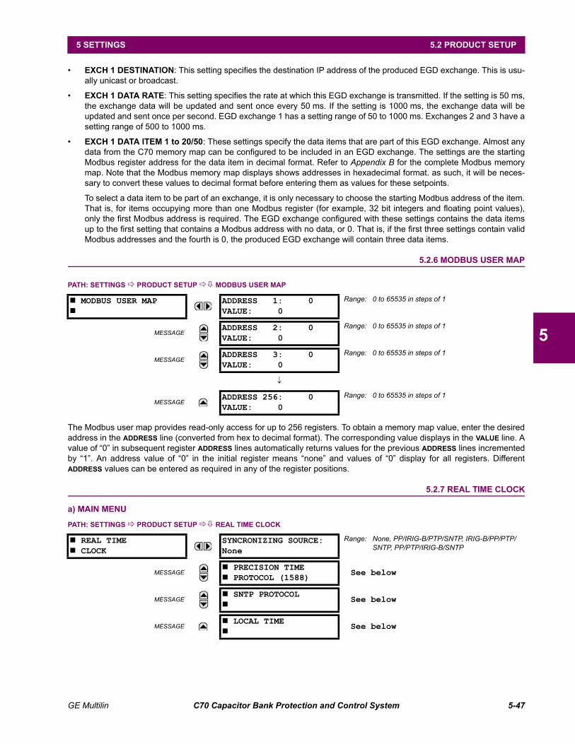
GE Multilin C70 Capacitor Bank Protection and Control System 5-47
5 SETTINGS 5.2 PRODUCT SETUP
5
• EXCH 1 DESTINATION: This setting specifies the destination IP address of the produced EGD exchange. This is usu-ally unicast or broadcast.
• EXCH 1 DATA RATE: This setting specifies the rate at which this EGD exchange is transmitted. If the setting is 50 ms,the exchange data will be updated and sent once every 50 ms. If the setting is 1000 ms, the exchange data will beupdated and sent once per second. EGD exchange 1 has a setting range of 50 to 1000 ms. Exchanges 2 and 3 have asetting range of 500 to 1000 ms.
• EXCH 1 DATA ITEM 1 to 20/50: These settings specify the data items that are part of this EGD exchange. Almost anydata from the C70 memory map can be configured to be included in an EGD exchange. The settings are the startingModbus register address for the data item in decimal format. Refer to Appendix B for the complete Modbus memorymap. Note that the Modbus memory map displays shows addresses in hexadecimal format. as such, it will be neces-sary to convert these values to decimal format before entering them as values for these setpoints.
To select a data item to be part of an exchange, it is only necessary to choose the starting Modbus address of the item.That is, for items occupying more than one Modbus register (for example, 32 bit integers and floating point values),only the first Modbus address is required. The EGD exchange configured with these settings contains the data itemsup to the first setting that contains a Modbus address with no data, or 0. That is, if the first three settings contain validModbus addresses and the fourth is 0, the produced EGD exchange will contain three data items.
5.2.6 MODBUS USER MAP
PATH: SETTINGS PRODUCT SETUP MODBUS USER MAP
The Modbus user map provides read-only access for up to 256 registers. To obtain a memory map value, enter the desiredaddress in the ADDRESS line (converted from hex to decimal format). The corresponding value displays in the VALUE line. Avalue of “0” in subsequent register ADDRESS lines automatically returns values for the previous ADDRESS lines incrementedby “1”. An address value of “0” in the initial register means “none” and values of “0” display for all registers. DifferentADDRESS values can be entered as required in any of the register positions.
5.2.7 REAL TIME CLOCK
a) MAIN MENU
PATH: SETTINGS PRODUCT SETUP REAL TIME CLOCK
MODBUS USER MAP
ADDRESS 1: 0VALUE: 0
Range: 0 to 65535 in steps of 1
MESSAGEADDRESS 2: 0VALUE: 0
Range: 0 to 65535 in steps of 1
MESSAGEADDRESS 3: 0VALUE: 0
Range: 0 to 65535 in steps of 1
MESSAGEADDRESS 256: 0VALUE: 0
Range: 0 to 65535 in steps of 1
REAL TIME CLOCK
SYNCRONIZING SOURCE:None
Range: None, PP/IRIG-B/PTP/SNTP, IRIG-B/PP/PTP/SNTP, PP/PTP/IRIG-B/SNTP
MESSAGE PRECISION TIME PROTOCOL (1588)
See below
MESSAGE SNTP PROTOCOL
See below
MESSAGE LOCAL TIME
See below

5-48 C70 Capacitor Bank Protection and Control System GE Multilin
5.2 PRODUCT SETUP 5 SETTINGS
5
The relay contains a real time clock (RTC) to create timestamps for communications protocols as well as for historical data,such as event records and oscillography. When the relay restarts, the RTC initializes from an onboard battery-backedclock, which has the same accuracy as an electronic watch, approximately ±1 minute per month (~23 ppm). Once the RTCis synchronized with the Precision Time Protocol (PTP), IRIG-B, or SNTP, its accuracy approaches that of the synchroniz-ing time delivered to the relay.
The SYNCHRONIZING SOURCE setting configures the priority sequence that the relay uses to determine which of theavailable external time sources synchronizes the RTC and the synchrophasor clock. A setting of None causes the RTC andthe synchrophasor clock to free-run. A setting of PP/IRIGB/PTP/SNTP, IRIGB/PP/PTP/SNTP, or PP/PTP/IRIGB/SNTPcauses the relay to track the first source named that is enabled and operational, or free-run if none of these are available.Here, PP means a time source that is strictly compliant with PP, PTP means a time source that is not strictly compliant withPP. When a time source fails or recovers, the relay automatically transfers synchronization as required by this setting.
See the COMMANDS SET DATE AND TIME menu item section of this manual to manually set the RTC.
To enable IRIG-B synchronization, the input IRIG-B signal type must be set to DC Shift or Amplitude Modulated using theSettings > Product Setup > Real Time Clock > IRIG-B > IRIG-B Signal Type setting. IRIG-B synchronization can be dis-abled by making this setting None.
To configure and enable PTP and/or SNTP, or to set local time parameters (for example time zone, daylight savings), usethe following sections.
b) PRECISION TIME PROTOCOL (1588)
PATH: SETTINGS PRODUCT SETUP REAL TIME CLOCK PRECISION TIME PROTOCOL (1588)
PATH: SETTINGS PRODUCT SETUP REAL TIME CLOCK PRECISION TIME PROTOCOL (1588) PTP PORT 1(3)
The UR supports the Precision Time Protocol (PTP) specified in IEEE Std 1588 2008 using the Power Profile (PP) specifiedin IEEE Std C37.238 2011. This enables the relay to synchronize to the international time standard over an Ethernet net-work that implements PP.
The relay can be configured to operate on some PTP networks that are not strictly PP. Time accuracy can be less thanspecified for a PP network. Tolerated deviations from strict PP include 1) missing declaration of PP compliance in the mes-sages, 2) connection to a network device that does not support the PTP peer delay mechanism, 3) jitter substantiallygreater than 1 µs in received event messages, and 4) certain non-compliant announce and sync message update rates.
The relay implements PTP according to IEEE Std 1588 2008 and the equivalent IEC 61588:2009(E), sometimesreferred to as version 2 PTP. It does not support the previous version of the standard (version 1).
PRECISION TIME PROTOCOL (1588)
STRICT POWER PROFILE:Disabled
Range: Enabled, Disabled
MESSAGEPTP DOMAIN NUMBER0
Range: 0 to 255
MESSAGEPTP VLAN PRIORITY4
Range: 0 to 7
PTP VLAN ID0
Range: 0 to 4095
MESSAGE PTP PORT 1
MESSAGEPORT 1 PTP FUNCTION:Disabled
Range: Enabled, Disabled
MESSAGEPORT 1 PATH DELAYADDER: 00000 ns
Range: 0 to 60 000 ns in steps of 1
MESSAGEPORT 1 PATH DELAYASYMMETRY: 0000 ns
Range: –1 000 to +1 000 ns in steps of 1
NOTE

GE Multilin C70 Capacitor Bank Protection and Control System 5-49
5 SETTINGS 5.2 PRODUCT SETUP
5
PTP is a protocol that allows multiple clocks in a network to synchronize with one another. It permits synchronization accu-racies better than 1 ns, but this requires each and every component in the network achieve very high levels of accuracy anda very high baud rate, faster than normally used for relay communications. When operating over a generic Ethernet net-work, time error may amount to 1 ms or more. PP is a profile of PTP which specifies a limited subset of PTP suitable for usein power system protection, control, automation and data communication applications, and thereby facilitates interoperabil-ity between different vendor’s clocks and switches. PP specifies a worst-case delivered time error of less than 1 µs over a16-hop network.
In a PTP system and in a PP system, the clocks automatically organize themselves into a master-slave synchronizationhierarchy with the “best” clock available making itself the "grandmaster" at the top of the hierarchy; all others make them-selves “slaves” and track the grandmaster. Typically the grandmaster clock receives its time from GPS satellites or someother link to the international time standard. If the grandmaster fails, the next “best” clock available in the domain assumesthe grandmaster role. Should a clock on starting up discover it is “better” that the present grandmaster, it assumes thegrandmaster role and the previous grandmaster reverts to slave.
Time messages issued by the grandmaster are delayed as they pass through the network both due to the finite speed ofthe signal in the interconnecting fiber or wire. Each clock and switch implementing PP measures the propagation delay toeach of its PP neighbors, and compensates for these delays in the time received. Each network device implementing PPmeasures the processing delay it introduces in each time message and compensates for this delay in the time it transmits.As a result, the time delivered to end-devices such as the UR are virtually identical to the grandmaster time. Should one ofthe network devices in the hierarchy not fully implement PP, the associated propagation delay and/or latency may not becompensated for, and the time received at the end-device could be in error by more than 100 µs.
See the Settings > Product Setup > Real Time Clock section of this manual for a description of when time valuesreceived via PTP are used to update the relay’s real time clock.
The following settings are available for configuring the relay for PTP.
PORT 1 ... 3 FUNCTION
• While this port setting is selected to disabled, PTP is disabled on this port. The relay does not generate or listen toPTP messages on this port.
PORT 1 ... 3 PATH DELAY ADDER
• The time delivered by PTP is advanced by the time value in this setting prior to the time being used to synchronize therelay’s real time clock. This is to compensate to the extent practical for time delivery delays not compensated for in thenetwork. In a fully compliant PP network, the peer delay and the processing delay mechanisms compensate for all thedelays between the grandmaster and the relay. In such networks, this setting should be zero.
• In networks containing one or more switches and/or clocks that do not implement both of these mechanisms, not alldelays are compensated, so the time of message arrival at the relay will be later than the time indicated in the mes-sage. This setting can be used to approximately compensate for this delay. However, as the relay is not aware of net-work switching that dynamically changes the amount of uncompensated delay, there is no setting that will alwayscompletely correct for uncompensated delay. A setting can be chosen that will reduce worst-case error to half of therange between minimum and maximum uncompensated delay, if these values are known.
PORT 1 ... 3 PATH DELAY ASYMMETRY
• This setting corresponds to “delayAsymmetry” in PTP, which is used by the peer delay mechanism to compensate forany difference in the propagation delay between the two directions of a link. Except in unusual cases, the two fibers areof essentially identical length and composition, so this setting should be set to zero.
• In unusual cases where the length of the link is different in different directions, this setting should be set to the numberof nanoseconds the Ethernet propagation delay to the relay is longer than the mean of path propagation delays to andfrom the relay. For instance, if it is known say from the physical length of the fibers and the propagation speed in thefibers that the delay from the relay to the Ethernet switch it is connected to is 9 000 ns and the that the delay from theswitch to the relay is 11 000 ns, then the mean delay is 10 000 ns, and the path delay asymmetry is 11000 - 10000 =+1000 ns.
STRICT POWER PROFILE
• Power profile (IEEE Std C37.238 2011) requires that the relay only select as a grandmaster power profile compliantclocks, that the delivered time have worst-case error of ±1 µs, and that the peer delay mechanism be implemented.With the strict power profile setting enabled, the relay will only select as master clocks displaying the IEEE_C37_238identification codes. It will use a port only when the peer delay mechanism is operational. With the strict power profile

5-50 C70 Capacitor Bank Protection and Control System GE Multilin
5.2 PRODUCT SETUP 5 SETTINGS
5
setting disabled, the relay will use clocks without the power profile identification when no power profile clocks are pres-ent, and will use ports even if the peer delay mechanism is non-operational.
• This setting applies to all of the relay’s PTP capable ports.
PTP DOMAIN NUMBER
• This setting should be set to the domain number of the grandmaster-capable clock(s) to be synchronized to. A net-work may support multiple time distribution domains, each distinguished with a unique domain number. More com-monly, there is a single domain using the default domain number zero.
• This setting applies to all of the relay’s PTP capable ports.
PTP VLAN PRIORITY
• This setting selects the value of the priority field in the 802.1Q VLAN tag in request messages issued by the relay’speer delay mechanism. In compliance with PP the default VLAN priority is 4, but it is recommended that in accordancewith PTP it be set to 7.
• Depending on the characteristics of the device to which the relay is directly linked, VLAN Priority may have no effect.
• This setting applies to all of the relay’s PTP capable ports.
PTP VLAN ID
• This setting selects the value of the ID field in the 802.1Q VLAN tag in request messages issued by the relay’s peerdelay mechanism. It is provided in compliance with PP. As these messages have a destination address that indicatesthey are not to be bridged, their VLAN ID serves no function, and so may be left at its default value.
• Depending on the characteristics of the device to which the relay is directly linked, VLAN ID may have no effect.
• This setting applies to all of the relay’s PTP capable ports.
c) SNTP PROTOCOL
PATH: SETTINGS PRODUCT SETUP REAL TIME CLOCK SNTP PROTOCOL
The C70 supports the Simple Network Time Protocol specified in RFC-2030. With SNTP, the C70 can obtain clock timeover an Ethernet network. The C70 acts as an SNTP client to receive time values from an SNTP/NTP server, usually a ded-icated product using a GPS receiver to provide an accurate time. Unicast SNTP is supported. The UR-series relays do notsupport the broadcast, multicast or anycast SNTP functionality.
The SNTP FUNCTION setting enables or disabled the SNTP feature on the C70.
To use SNTP, SNTP SERVER IP ADDR must be set to the SNTP/NTP server IP address. Once this address is set and SNTP
FUNCTION is “Enabled”, the C70 attempts to obtain time values from the SNTP/NTP server. Since many time values areobtained and averaged, it generally takes three to four minutes until the C70 clock is closely synchronized with the SNTP/NTP server. It takes up to two minutes for the C70 to signal an SNTP self-test error if the server is offline.
The SNTP UDP PORT NUMBER is 123 for normal SNTP operation. If SNTP is not required, close the port by setting it to 0.
When the SNTP UDP PORT NUMBER is set to 0, the change takes effect when the C70 is restarted.
SNTP PROTOCOL
SNTP FUNCTION:Disabled
Range: Enabled, Disabled
MESSAGESNTP SERVER IP ADDR:0.0.0.0
Range: Standard IP address format
MESSAGESNTP UDP PORTNUMBER: 123
Range: 0 to 65535 in steps of 1
NOTE

GE Multilin C70 Capacitor Bank Protection and Control System 5-51
5 SETTINGS 5.2 PRODUCT SETUP
5
d) LOCAL TIME
PATH: SETTINGS PRODUCT SETUP REAL TIME CLOCK LOCAL TIME
The UR device maintains two times: local time and Universal Coordinated Time (UTC). Local time can be provided by IRIG-B signals. UTC time is provided by SNTP servers.
The real-time clock (RTC) and communication protocol times are not correct unless Local Time is configured for the currentlocation. When the RTC is synchronized with IRIG-B, Local Time must be configured for the current location or else thetimestamps may not be accurate. Furthermore, times reported in historical records and communication protocols may beincorrect if the Local Time setting is not configured properly.
The LOCAL TIME OFFSET FROM UTC setting is used to specify the local time zone offset from UTC (Greenwich Mean Time) inhours. Time zones in the eastern hemisphere have positive values; time zones in the western hemisphere have negativevalues. A value of zero causes the relay to use UTC for local time. This setting has two uses. When the system RTC is syn-chronized with a communications protocol providing only local time or it is free-running, the offset setting is used to calcu-late UTC from the local time these provide. When the RTC is synchronized with a communications protocol providing onlyUTC (such as PTP or SNTP), the time offset setting is used to determine local time from the UTC provided. PTPALTERNATE_TIME_OFFSET_INDICATOR TLVs are not used to calculate local time. When a communications protocolother than PTP provides UTC to local time offset (meaning IRIG-B), that offset is used instead of the local time and daylighttime settings.
The DAYLIGHT SAVINGS TIME (DST) settings can be used to allow the relay to follow the DST rules of the local time zone.Note that when IRIG-B time synchronization is active, the local time in the IRIG-B signal contains any daylight savings timeoffset and so the DST settings are ignored.
LOCAL TIME
LOCAL TIME OFFSETFROM UTC: 0.0 hrs
Range: –24.0 to 24.0 hrs in steps of 0.5
MESSAGEDAYLIGHT SAVINGSTIME: Disabled
Range: Disabled, Enabled
MESSAGEDST START MONTH:January
Range: January to December (all months)
MESSAGEDST START DAY:Sunday
Range: Sunday to Saturday (all days of the week)
MESSAGEDST START DAYINSTANCE: First
Range: First, Second, Third, Fourth, Last
MESSAGEDST START HOUR:2
Range: 0 to 23
MESSAGEDST STOP MONTH:January
Range: January to December (all months)
MESSAGEDST STOP DAY:Sunday
Range: Sunday to Saturday (all days of the week)
MESSAGEDST STOP DAYINSTANCE: First
Range: First, Second, Third, Fourth, Last
MESSAGEDST STOP HOUR:2
Range: 0 to 23

5-52 C70 Capacitor Bank Protection and Control System GE Multilin
5.2 PRODUCT SETUP 5 SETTINGS
5
5.2.8 USER-PROGRAMMABLE FAULT REPORTS
PATH: SETTINGS PRODUCT SETUP USER-PROGRAMMABLE FAULT REPORT USER-PROGRAMMABLE FAULT REPORT 1(2)
When enabled, this function monitors the pre-fault trigger. The pre-fault data are stored in the memory for prospective cre-ation of the fault report on the rising edge of the pre-fault trigger. The element waits for the fault trigger as long as the pre-fault trigger is asserted, but not shorter than 1 second. When the fault trigger occurs, the fault data is stored and the com-plete report is created. If the fault trigger does not occur within 1 second after the pre-fault trigger drops out, the elementresets and no record is created.
The user programmable record contains the following information: the user-programmed relay name, detailed firmwarerevision (7.0x, for example) and relay model (C70), the date and time of trigger, the name of pre-fault trigger (a specificFlexLogic operand), the name of fault trigger (a specific FlexLogic operand), the active setting group at pre-fault trigger, theactive setting group at fault trigger, pre-fault values of all programmed analog channels (one cycle before pre-fault trigger),and fault values of all programmed analog channels (at the fault trigger).
Each fault report is stored as a file to a maximum capacity of ten files. An eleventh trigger overwrites the oldest file. TheEnerVista UR Setup software is required to view all captured data. A FAULT RPT TRIG event is automatically created whenthe report is triggered.
The relay includes two user-programmable fault reports to enable capture of two types of trips (for example, trip from ther-mal protection with the report configured to include temperatures, and short-circuit trip with the report configured to includevoltages and currents). Both reports feed the same report file queue.
The last record is available as individual data items via communications protocols.
• PRE-FAULT 1 TRIGGER: Specifies the FlexLogic operand to capture the pre-fault data. The rising edge of this oper-and stores one cycle-old data for subsequent reporting. The element waits for the fault trigger to actually create arecord as long as the operand selected as PRE-FAULT 1 TRIGGER is “On”. If the operand remains “Off” for 1 second, theelement resets and no record is created.
• FAULT 1 TRIGGER: Specifies the FlexLogic operand to capture the fault data. The rising edge of this operand storesthe data as fault data and results in a new report. The trigger (not the pre-fault trigger) controls the date and time of thereport.
• FAULT REPORT 1 #1 to FAULT REPORT 1 #32: These settings specify an actual value such as voltage or currentmagnitude, true RMS, phase angle, frequency, temperature, etc., to be stored should the report be created. Up to 32channels can be configured. Two reports are configurable to cope with variety of trip conditions and items of interest.
USER-PROGRAMMABLE FAULT REPORT 1
FAULT REPORT 1FUNCTION: Disabled
Range: Disabled, Enabled
MESSAGEPRE-FAULT 1 TRIGGER:Off
Range: FlexLogic operand
MESSAGEFAULT 1 TRIGGER:Off
Range: FlexLogic operand
MESSAGEFAULT REPORT 1 #1:Off
Range: Off, any actual value analog parameter
MESSAGEFAULT REPORT 1 #2:Off
Range: Off, any actual value analog parameter
MESSAGEFAULT REPORT 1 #3:Off
Range: Off, any actual value analog parameter
MESSAGEFAULT REPORT 1 #32:Off
Range: Off, any actual value analog parameter

GE Multilin C70 Capacitor Bank Protection and Control System 5-53
5 SETTINGS 5.2 PRODUCT SETUP
5
5.2.9 OSCILLOGRAPHY
a) MAIN MENU
PATH: SETTINGS PRODUCT SETUP OSCILLOGRAPHY
Oscillography records contain waveforms captured at the sampling rate as well as other relay data at the point of trigger.Oscillography records are triggered by a programmable FlexLogic operand. Multiple oscillography records may be capturedsimultaneously.
The NUMBER OF RECORDS is selectable, but the number of cycles captured in a single record varies considerably based onother factors such as sample rate and the number of operational modules. There is a fixed amount of data storage for oscil-lography; the more data captured, the less the number of cycles captured per record. See the ACTUAL VALUES RECORDS OSCILLOGRAPHY menu to view the number of cycles captured per record. The following table provides sam-ple configurations with corresponding cycles/record. The minimum number of oscillographic records is three.
A new record may automatically overwrite an older record if TRIGGER MODE is set to “Automatic Overwrite”.
Set the TRIGGER POSITION to a percentage of the total buffer size (for example, 10%, 50%, 75%, etc.). A trigger position of25% consists of 25% pre- and 75% post-trigger data. The TRIGGER SOURCE is always captured in oscillography and may beany FlexLogic parameter (element state, contact input, virtual output, etc.). The relay sampling rate is 64 samples per cycle.
The AC INPUT WAVEFORMS setting determines the sampling rate at which AC input signals (that is, current and voltage) arestored. Reducing the sampling rate allows longer records to be stored. This setting has no effect on the internal samplingrate of the relay which is always 64 samples per cycle; that is, it has no effect on the fundamental calculations of the device.
When changes are made to the oscillography settings, all existing oscillography records will be CLEARED.
OSCILLOGRAPHY
NUMBER OF RECORDS:15
Range: 1 to 64 in steps of 1
MESSAGETRIGGER MODE:Automatic Overwrite
Range: Automatic Overwrite, Protected
MESSAGETRIGGER POSITION:50%
Range: 0 to 100% in steps of 1
MESSAGETRIGGER SOURCE:Off
Range: FlexLogic operand
MESSAGEAC INPUT WAVEFORMS:16 samples/cycle
Range: Off; 8, 16, 32, 64 samples/cycle
MESSAGE DIGITAL CHANNELS
MESSAGE ANALOG CHANNELS
Table 5–2: OSCILLOGRAPHY CYCLES/RECORD EXAMPLE
RECORDS CT/VTS SAMPLERATE
DIGITALS ANALOGS CYCLES/RECORD
3 1 8 0 0 14663
3 1 16 16 0 6945
8 1 16 16 0 3472
8 1 16 16 4 2868
8 2 16 16 4 1691
8 2 16 63 16 1221
8 2 32 63 16 749
8 2 64 63 16 422
32 2 64 63 16 124
NOTE

5-54 C70 Capacitor Bank Protection and Control System GE Multilin
5.2 PRODUCT SETUP 5 SETTINGS
5
b) DIGITAL CHANNELS
PATH: SETTINGS PRODUCT SETUP OSCILLOGRAPHY DIGITAL CHANNELS
A DIGITAL 1(63) CHANNEL setting selects the FlexLogic operand state recorded in an oscillography trace. The length of eachoscillography trace depends in part on the number of parameters selected here. Parameters set to “Off” are ignored. Uponstartup, the relay will automatically prepare the parameter list.
c) ANALOG CHANNELS
PATH: SETTINGS PRODUCT SETUP OSCILLOGRAPHY ANALOG CHANNELS
These settings select the metering actual value recorded in an oscillography trace. The length of each oscillography tracedepends in part on the number of parameters selected here. Parameters set to “Off” are ignored. The parameters availablein a given relay are dependent on:
• The type of relay,
• The type and number of CT/VT hardware modules installed, and
• The type and number of analog input hardware modules installed.
Upon startup, the relay will automatically prepare the parameter list. A list of all possible analog metering actual valueparameters is presented in Appendix A: FlexAnalog parameters. The parameter index number shown in any of the tables isused to expedite the selection of the parameter on the relay display. It can be quite time-consuming to scan through the listof parameters via the relay keypad and display - entering this number via the relay keypad will cause the correspondingparameter to be displayed.
All eight CT/VT module channels are stored in the oscillography file. The CT/VT module channels are named as follows:
<slot_letter><terminal_number>—<I or V><phase A, B, or C, or 4th input>
The fourth current input in a bank is called IG, and the fourth voltage input in a bank is called VX. For example, F2-IB desig-nates the IB signal on terminal 2 of the CT/VT module in slot F.
If there are no CT/VT modules and analog input modules, no analog traces will appear in the file; only the digital traces willappear.
DIGITAL CHANNELS
DIGITAL CHANNEL 1:Off
Range: FlexLogic operand
MESSAGEDIGITAL CHANNEL 2:Off
Range: FlexLogic operand
MESSAGEDIGITAL CHANNEL 3:Off
Range: FlexLogic operand
MESSAGEDIGITAL CHANNEL 63:Off
Range: FlexLogic operand
ANALOG CHANNELS
ANALOG CHANNEL 1:Off
Range: Off, any FlexAnalog parameterSee Appendix A for complete list.
MESSAGEANALOG CHANNEL 2:Off
Range: Off, any FlexAnalog parameterSee Appendix A for complete list.
MESSAGEANALOG CHANNEL 3:Off
Range: Off, any FlexAnalog parameterSee Appendix A for complete list.
MESSAGEANALOG CHANNEL 16:Off
Range: Off, any FlexAnalog parameterSee Appendix A for complete list.

GE Multilin C70 Capacitor Bank Protection and Control System 5-55
5 SETTINGS 5.2 PRODUCT SETUP
5
The source harmonic indices appear as oscillography analog channels numbered from 0 to 23. These corresponddirectly to the to the 2nd to 25th harmonics in the relay as follows:
Analog channel 0 2nd harmonicAnalog channel 1 3rd harmonic
...Analog channel 23 25th harmonic
5.2.10 DATA LOGGER
PATH: SETTINGS PRODUCT SETUP DATA LOGGER
The data logger samples and records up to 16 analog parameters at a user-defined sampling rate. This recorded data maybe downloaded to EnerVista UR Setup and displayed with parameters on the vertical axis and time on the horizontal axis.All data is stored in non-volatile memory, meaning that the information is retained when power to the relay is lost.
For a fixed sampling rate, the data logger can be configured with a few channels over a long period or a larger number ofchannels for a shorter period. The relay automatically partitions the available memory between the channels in use. Exam-ple storage capacities for a system frequency of 60 Hz are shown in the following table.
DATA LOGGER
DATA LOGGER MODE:Continuous
Range: Continuous, Trigger
MESSAGEDATA LOGGER TRIGGER:Off
Range: FlexLogic operand
MESSAGEDATA LOGGER RATE:60000 ms
Range: 15 to 3600000 ms in steps of 1
MESSAGEDATA LOGGER CHNL 1:Off
Range: Off, any FlexAnalog parameter. See Appendix A:FlexAnalog Parameters for complete list.
MESSAGEDATA LOGGER CHNL 2:Off
Range: Off, any FlexAnalog parameter. See Appendix A:FlexAnalog Parameters for complete list.
MESSAGEDATA LOGGER CHNL 3:Off
Range: Off, any FlexAnalog parameter. See Appendix A:FlexAnalog Parameters for complete list.
MESSAGEDATA LOGGER CHNL 16:Off
Range: Off, any FlexAnalog parameter. See Appendix A:FlexAnalog Parameters for complete list.
MESSAGEDATA LOGGER CONFIG:0 CHNL x 0.0 DAYS
Range: Not applicable - shows computed data only
NOTE
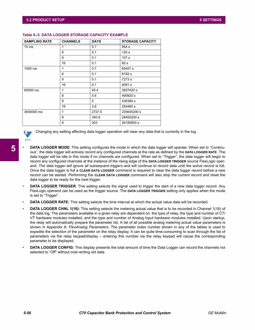
5-56 C70 Capacitor Bank Protection and Control System GE Multilin
5.2 PRODUCT SETUP 5 SETTINGS
5
Changing any setting affecting data logger operation will clear any data that is currently in the log.
• DATA LOGGER MODE: This setting configures the mode in which the data logger will operate. When set to “Continu-ous”, the data logger will actively record any configured channels at the rate as defined by the DATA LOGGER RATE. Thedata logger will be idle in this mode if no channels are configured. When set to “Trigger”, the data logger will begin torecord any configured channels at the instance of the rising edge of the DATA LOGGER TRIGGER source FlexLogic oper-and. The data logger will ignore all subsequent triggers and will continue to record data until the active record is full.Once the data logger is full a CLEAR DATA LOGGER command is required to clear the data logger record before a newrecord can be started. Performing the CLEAR DATA LOGGER command will also stop the current record and reset thedata logger to be ready for the next trigger.
• DATA LOGGER TRIGGER: This setting selects the signal used to trigger the start of a new data logger record. AnyFlexLogic operand can be used as the trigger source. The DATA LOGGER TRIGGER setting only applies when the modeis set to “Trigger”.
• DATA LOGGER RATE: This setting selects the time interval at which the actual value data will be recorded.
• DATA LOGGER CHNL 1(16): This setting selects the metering actual value that is to be recorded in Channel 1(16) ofthe data log. The parameters available in a given relay are dependent on: the type of relay, the type and number of CT/VT hardware modules installed, and the type and number of Analog Input hardware modules installed. Upon startup,the relay will automatically prepare the parameter list. A list of all possible analog metering actual value parameters isshown in Appendix A: FlexAnalog Parameters. The parameter index number shown in any of the tables is used toexpedite the selection of the parameter on the relay display. It can be quite time-consuming to scan through the list ofparameters via the relay keypad/display – entering this number via the relay keypad will cause the correspondingparameter to be displayed.
• DATA LOGGER CONFIG: This display presents the total amount of time the Data Logger can record the channels notselected to “Off” without over-writing old data.
Table 5–3: DATA LOGGER STORAGE CAPACITY EXAMPLE
SAMPLING RATE CHANNELS DAYS STORAGE CAPACITY
15 ms 1 0.1 954 s
8 0.1 120 s
9 0.1 107 s
16 0.1 60 s
1000 ms 1 0.7 65457 s
8 0.1 8182 s
9 0.1 7273 s
16 0.1 4091 s
60000 ms 1 45.4 3927420 s
8 5.6 490920 s
9 5 436380 s
16 2.8 254460 s
3600000 ms 1 2727.5 235645200 s
8 340.9 29455200 s
9 303 26182800 s
NOTE

GE Multilin C70 Capacitor Bank Protection and Control System 5-57
5 SETTINGS 5.2 PRODUCT SETUP
5
5.2.11 USER-PROGRAMMABLE LEDS
a) MAIN MENU
PATH: SETTINGS PRODUCT SETUP USER-PROGRAMMABLE LEDS
The 48 amber LEDs on relay panels 2 and 3 can be customized to illuminate when a selected FlexLogic operand is in thelogic 1 state. The trip and alarm LEDs on panel 1 can also be customized in a similar manner. To ensure correct functional-ity of all LEDs, an LED test feature is also provided.
b) LED TEST
PATH: SETTINGS PRODUCT SETUP USER-PROGRAMMABLE LEDS LED TEST
When enabled, the LED test can be initiated from any digital input or user-programmable condition such as user-program-mable pushbutton. The control operand is configured under the LED TEST CONTROL setting. The test covers all LEDs,including the LEDs of the optional user-programmable pushbuttons.
The test consists of three stages.
1. All 62 LEDs on the relay are illuminated. This is a quick test to verify if any of the LEDs is “burned”. This stage lasts aslong as the control input is on, up to a maximum of 1 minute. After 1 minute, the test will end.
2. All the LEDs are turned off, and then one LED at a time turns on for 1 second, then back off. The test routine starts atthe top left panel, moving from the top to bottom of each LED column. This test checks for hardware failures that leadto more than one LED being turned on from a single logic point. This stage can be interrupted at any time.
3. All the LEDs are turned on. One LED at a time turns off for 1 second, then back on. The test routine starts at the top leftpanel moving from top to bottom of each column of the LEDs. This test checks for hardware failures that lead to morethan one LED being turned off from a single logic point. This stage can be interrupted at any time.
When testing is in progress, the LEDs are controlled by the test sequence, rather than the protection, control, and monitor-ing features. However, the LED control mechanism accepts all the changes to LED states generated by the relay andstores the actual LED states (on or off) in memory. When the test completes, the LEDs reflect the actual state resulting fromrelay response during testing. The reset pushbutton will not clear any targets when the LED Test is in progress.
A dedicated FlexLogic operand, LED TEST IN PROGRESS, is set for the duration of the test. When the test sequence is initi-ated, the LED TEST INITIATED event is stored in the event recorder.
The entire test procedure is user-controlled. In particular, stage 1 can last as long as necessary, and stages 2 and 3 can beinterrupted. The test responds to the position and rising edges of the control input defined by the LED TEST CONTROL set-ting. The control pulses must last at least 250 ms to take effect. The following diagram explains how the test is executed.
USER-PROGRAMMABLE LEDS
LED TEST
See below
MESSAGE TRIP & ALARM LEDS
See page 5–59.
MESSAGE USER-PROGRAMMABLE LED 1
See page 5–59.
MESSAGE USER-PROGRAMMABLE LED 2
MESSAGE USER-PROGRAMMABLE LED 48
LED TEST
LED TEST FUNCTION:Disabled
Range: Disabled, Enabled.
MESSAGELED TEST CONTROL:Off
Range: FlexLogic operand
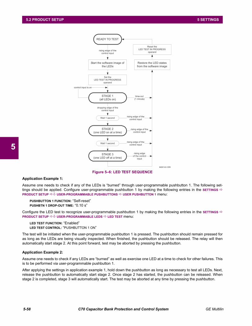
5-58 C70 Capacitor Bank Protection and Control System GE Multilin
5.2 PRODUCT SETUP 5 SETTINGS
5
Figure 5–6: LED TEST SEQUENCE
Application Example 1:
Assume one needs to check if any of the LEDs is “burned” through user-programmable pushbutton 1. The following set-tings should be applied. Configure user-programmable pushbutton 1 by making the following entries in the SETTINGS PRODUCT SETUP USER-PROGRAMMABLE PUSHBUTTONS USER PUSHBUTTON 1 menu:
PUSHBUTTON 1 FUNCTION: “Self-reset”PUSHBTN 1 DROP-OUT TIME: “0.10 s”
Configure the LED test to recognize user-programmable pushbutton 1 by making the following entries in the SETTINGS PRODUCT SETUP USER-PROGRAMMABLE LEDS LED TEST menu:
LED TEST FUNCTION: “Enabled”LED TEST CONTROL: “PUSHBUTTON 1 ON”
The test will be initiated when the user-programmable pushbutton 1 is pressed. The pushbutton should remain pressed foras long as the LEDs are being visually inspected. When finished, the pushbutton should be released. The relay will thenautomatically start stage 2. At this point forward, test may be aborted by pressing the pushbutton.
Application Example 2:
Assume one needs to check if any LEDs are “burned” as well as exercise one LED at a time to check for other failures. Thisis to be performed via user-programmable pushbutton 1.
After applying the settings in application example 1, hold down the pushbutton as long as necessary to test all LEDs. Next,release the pushbutton to automatically start stage 2. Once stage 2 has started, the pushbutton can be released. Whenstage 2 is completed, stage 3 will automatically start. The test may be aborted at any time by pressing the pushbutton.
842011A1.CDR
READY TO TEST
Start the software image of
the LEDs
STAGE 1
(all LEDs on)
control input is on
Wait 1 second
dropping edge of the
control input
Restore the LED states
from the software image
rising edge of the
control input
STAGE 2
(one LED on at a time)
STAGE 3
(one LED off at a time)
rising edge
of the control
input
rising edge of the
control input
Set the
LED TEST IN PROGRESS
operand
Reset the
LED TEST IN PROGRESS
operand
rising edge of the
control input
Wait 1 secondrising edge of the
control input
time-out
(1 minute)

GE Multilin C70 Capacitor Bank Protection and Control System 5-59
5 SETTINGS 5.2 PRODUCT SETUP
5
c) TRIP AND ALARM LEDS
PATH: SETTINGS PRODUCT SETUP USER-PROGRAMMABLE LEDS TRIP & ALARM LEDS
The trip and alarm LEDs are in the first LED column (enhanced faceplate) and on LED panel 1 (standard faceplate). Eachindicator can be programmed to become illuminated when the selected FlexLogic operand is in the logic 1 state.
d) USER-PROGRAMMABLE LED 1(48)
PATH: SETTINGS PRODUCT SETUP USER-PROGRAMMABLE LEDS USER-PROGRAMMABLE LED 1(48)
There are 48 amber LEDs across the relay faceplate LED panels. Each of these indicators can be programmed to illumi-nate when the selected FlexLogic operand is in the logic 1 state.
For the standard faceplate, the LEDs are located as follows.
• LED Panel 2: user-programmable LEDs 1 through 24
• LED Panel 3: user programmable LEDs 25 through 48
For the enhanced faceplate, the LEDs are located as follows.
• LED column 2: user-programmable LEDs 1 through 12
• LED column 3: user-programmable LEDs 13 through 24
• LED column 4: user-programmable LEDs 25 through 36
• LED column 5: user-programmable LEDs 37 through 48
Refer to the LED indicators section in chapter 4 for additional information on the location of these indexed LEDs.
The user-programmable LED settings select the FlexLogic operands that control the LEDs. If the LED 1 TYPE setting is “Self-Reset” (the default setting), the LED illumination will track the state of the selected LED operand. If the LED 1 TYPE setting is“Latched”, the LED, once lit, remains so until reset by the faceplate RESET button, from a remote device via a communica-tions channel, or from any programmed operand, even if the LED operand state de-asserts.
TRIP & ALARM LEDS
TRIP LED INPUT:Off
Range: FlexLogic operand
MESSAGEALARM LED INPUT:Off
Range: FlexLogic operand
USER-PROGRAMMABLE LED 1
LED 1 OPERAND:Off
Range: FlexLogic operand
MESSAGELED 1 TYPE:Self-Reset
Range: Self-Reset, Latched
Table 5–4: RECOMMENDED SETTINGS FOR USER-PROGRAMMABLE LEDS
SETTING PARAMETER SETTING PARAMETER
LED 1 operand SETTING GROUP ACT 1 LED 13 operand Off
LED 2 operand SETTING GROUP ACT 2 LED 14 operand Off
LED 3 operand SETTING GROUP ACT 3 LED 15 operand Off
LED 4 operand SETTING GROUP ACT 4 LED 16 operand Off
LED 5 operand SETTING GROUP ACT 5 LED 17 operand Off
LED 6 operand SETTING GROUP ACT 6 LED 18 operand Off
LED 7 operand Off LED 19 operand Off
LED 8 operand Off LED 20 operand Off
LED 9 operand Off LED 21 operand Off
LED 10 operand Off LED 22 operand Off
LED 11 operand Off LED 23 operand Off
LED 12 operand Off LED 24 operand Off

5-60 C70 Capacitor Bank Protection and Control System GE Multilin
5.2 PRODUCT SETUP 5 SETTINGS
5
Refer to the Control of setting groups example in the Control elements section of this chapter for group activation.
5.2.12 USER-PROGRAMMABLE SELF TESTS
For user-programmable self-tests for CyberSentry, use the Setup > Security > Supervisory menu instead.
PATH: SETTINGS PRODUCT SETUP USER-PROGRAMMABLE SELF TESTS
All major self-test alarms are reported automatically with their corresponding FlexLogic operands, events, and targets. Mostof the minor alarms can be disabled if desired.
When in the “Disabled” mode, minor alarms will not assert a FlexLogic operand, write to the event recorder, or display tar-get messages. Moreover, they will not trigger the ANY MINOR ALARM or ANY SELF-TEST messages. When in the “Enabled”mode, minor alarms continue to function along with other major and minor alarms. Refer to the Relay self-tests section inchapter 7 for additional information on major and minor self-test alarms.
USER-PROGRAMMABLE SELF TESTS
DIRECT RING BREAKFUNCTION: Enabled
Range: Disabled, Enabled. Valid for units equipped withDirect Input/Output module.
MESSAGEDIRECT DEVICE OFFFUNCTION: Enabled
Range: Disabled, Enabled. Valid for units equipped withDirect Input/Output module.
MESSAGEREMOTE DEVICE OFFFUNCTION: Enabled
Range: Disabled, Enabled.
MESSAGEFIRST ETHERNET FAILFUNCTION: Disabled
Range: Disabled, Enabled.
MESSAGESEC. ETHERNET FAILFUNCTION: Disabled
Range: Disabled, Enabled.
MESSAGETHIRD ETHERNET FAILFUNCTION: Disabled
Range: Disabled, Enabled.
MESSAGEBATTERY FAILFUNCTION: Enabled
Range: Disabled, Enabled.
MESSAGESNTP FAILFUNCTION: Enabled
Range: Disabled, Enabled.
MESSAGEIRIG-B FAILFUNCTION: Enabled
Range: Disabled, Enabled.
MESSAGEPTP FAILFUNCTION: Enabled
Range: Disabled, Enabled.
MESSAGESFP MODULE FAILFUNCTION: Disabled
Range: Disabled, Enabled.

GE Multilin C70 Capacitor Bank Protection and Control System 5-61
5 SETTINGS 5.2 PRODUCT SETUP
5
5.2.13 CONTROL PUSHBUTTONS
PATH: SETTINGS PRODUCT SETUP CONTROL PUSHBUTTONS CONTROL PUSHBUTTON 1(7)
There are three standard control pushbuttons, labeled USER 1, USER 2, and USER 3, on the standard and enhanced frontpanels. These are user-programmable and can be used for various applications such as performing an LED test, switchingsetting groups, and invoking and scrolling though user-programmable displays.
The location of the control pushbuttons are shown in the following figures.
Figure 5–7: CONTROL PUSHBUTTONS (ENHANCED FACEPLATE)
An additional four control pushbuttons are included on the standard faceplate when the C70 is ordered with the twelveuser-programmable pushbutton option.
Figure 5–8: CONTROL PUSHBUTTONS (STANDARD FACEPLATE)
Control pushbuttons are not typically used for critical operations and are not protected by the control password. However,by supervising their output operands, the user can dynamically enable or disable control pushbuttons for security reasons.
Each control pushbutton asserts its own FlexLogic operand. These operands should be configured appropriately to performthe desired function. The operand remains asserted as long as the pushbutton is pressed and resets when the pushbuttonis released. A dropout delay of 100 ms is incorporated to ensure fast pushbutton manipulation will be recognized by variousfeatures that may use control pushbuttons as inputs.
An event is logged in the event record (as per user setting) when a control pushbutton is pressed. No event is logged whenthe pushbutton is released. The faceplate keys (including control keys) cannot be operated simultaneously – a given keymust be released before the next one can be pressed.
CONTROL PUSHBUTTON 1
CONTROL PUSHBUTTON 1FUNCTION: Disabled
Range: Disabled, Enabled
MESSAGECONTROL PUSHBUTTON 1EVENTS: Disabled
Range: Disabled, Enabled
Control pushbuttons
842813A1.CDR
842733A2.CDR
PICKUP
ALARM
TRIP
TEST MODE
TROUBLE
IN SERVICE
STATUS
USER 3
USER 2
USER 1
RESET
EVENT CAUSE
NEUTRAL/GROUND
PHASE C
PHASE B
PHASE A
OTHER
FREQUENCY
CURRENT
VOLTAGE
THREE
STANDARD
CONTROL
PUSHBUTTONS
USER 7
USER 6
USER 5
USER 4
FOUR EXTRA
OPTIONAL
CONTROL
PUSHBUTTONS

5-62 C70 Capacitor Bank Protection and Control System GE Multilin
5.2 PRODUCT SETUP 5 SETTINGS
5
Figure 5–9: CONTROL PUSHBUTTON LOGIC
5.2.14 USER-PROGRAMMABLE PUSHBUTTONS
PATH: SETTINGS PRODUCT SETUP USER-PROGRAMMABLE PUSHBUTTONS USER PUSHBUTTON 1(16)
USER PUSHBUTTON 1
PUSHBUTTON 1FUNCTION: Disabled
Range: Self-Reset, Latched, Disabled
MESSAGEPUSHBTN 1 ID TEXT: Range: Up to 20 alphanumeric characters
MESSAGEPUSHBTN 1 ON TEXT: Range: Up to 20 alphanumeric characters
MESSAGEPUSHBTN 1 OFF TEXT: Range: Up to 20 alphanumeric characters
MESSAGEPUSHBTN 1 HOLD:0.0 s
Range: 0.0 to 10.0 s in steps of 0.1
MESSAGEPUSHBTN 1 SET:Off
Range: FlexLogic operand
MESSAGEPUSHBTN 1 RESET:Off
Range: FlexLogic operand
MESSAGEPUSHBTN 1 AUTORST:Disabled
Range: Disabled, Enabled
MESSAGEPUSHBTN 1 AUTORSTDELAY: 1.0 s
Range: 0.2 to 600.0 s in steps of 0.1
MESSAGEPUSHBTN 1 REMOTE:Off
Range: FlexLogic operand
MESSAGEPUSHBTN 1 LOCAL:Off
Range: FlexLogic operand
MESSAGEPUSHBTN 1 DROP-OUTTIME: 0.00 s
Range: 0 to 60.00 s in steps of 0.05
MESSAGEPUSHBTN 1 LED CTL:Off
Range: FlexLogic operand
MESSAGEPUSHBTN 1 MESSAGE:Disabled
Range: Disabled, Normal, High Priority
MESSAGEPUSHBUTTON 1EVENTS: Disabled
Range: Disabled, Enabled
842010A2.CDR
CONTROL PUSHBUTTON1 FUNCTION:
SYSTEM SETUP/BREAKERS/BREAKER 1/BREAKER 1 PUSHBUTTON
:CONTROL
SYSTEM SETUP/BREAKERS/BREAKER 2/BREAKER 2 PUSHBUTTON
:CONTROL
SETTING
SETTINGS
TIMERFLEXLOGIC OPERAND
Enabled=1
Enabled=1
Whe
n ap
plic
able
Enabled=1
RUN
OFF
ON
AND
100 msec0 CONTROL PUSHBTN 1 ON

GE Multilin C70 Capacitor Bank Protection and Control System 5-63
5 SETTINGS 5.2 PRODUCT SETUP
5
The optional user-programmable pushbuttons (specified in the order code) provide an easy and error-free method of enter-ing digital state (on, off) information. The number of available pushbuttons is dependent on the faceplate module orderedwith the relay.
• Type P faceplate: standard horizontal faceplate with 12 user-programmable pushbuttons.
• Type Q faceplate: enhanced horizontal faceplate with 16 user-programmable pushbuttons.
The digital state can be entered locally (by directly pressing the front panel pushbutton) or remotely (via FlexLogic oper-ands) into FlexLogic equations, protection elements, and control elements. Typical applications include breaker control,autorecloser blocking, and setting groups changes. The user-programmable pushbuttons are under the control level ofpassword protection.
The user-configurable pushbuttons for the enhanced faceplate are shown below.
Figure 5–10: USER-PROGRAMMABLE PUSHBUTTONS (ENHANCED FACEPLATE)
The user-configurable pushbuttons for the standard faceplate are shown below.
Figure 5–11: USER-PROGRAMMABLE PUSHBUTTONS (STANDARD FACEPLATE)
Both the standard and enhanced faceplate pushbuttons can be custom labeled with a factory-provided template, availableonline at http://www.gedigitalenergy.com/multilin. The EnerVista UR Setup software can also be used to create labels forthe enhanced faceplate.
Each pushbutton asserts its own “On” and “Off” FlexLogic operands (for example, PUSHBUTTON 1 ON and PUSHBUTTON 1OFF). These operands are available for each pushbutton and are used to program specific actions. If any pushbutton isactive, the ANY PB ON operand will be asserted.
Each pushbutton has an associated LED indicator. By default, this indicator displays the present status of the correspond-ing pushbutton (on or off). However, each LED indicator can be assigned to any FlexLogic operand through the PUSHBTN 1
LED CTL setting.
The pushbuttons can be automatically controlled by activating the operands assigned to the PUSHBTN 1 SET (for latched andself-reset mode) and PUSHBTN 1 RESET (for latched mode only) settings. The pushbutton reset status is declared when thePUSHBUTTON 1 OFF operand is asserted. The activation and deactivation of user-programmable pushbuttons is dependenton whether latched or self-reset mode is programmed.
• Latched mode: In latched mode, a pushbutton can be set (activated) by asserting the operand assigned to the PUSH-
BTN 1 SET setting or by directly pressing the associated front panel pushbutton. The pushbutton maintains the set stateuntil deactivated by the reset command or after a user-specified time delay. The state of each pushbutton is stored innon-volatile memory and maintained through a loss of control power.
The pushbutton is reset (deactivated) in latched mode by asserting the operand assigned to the PUSHBTN 1 RESET set-ting or by directly pressing the associated active front panel pushbutton.
842814A1.CDR
USER
LABEL 1
USER
LABEL 2
USER
LABEL 3
USER
LABEL 4
USER
LABEL 5
USER
LABEL 6
USER
LABEL 7
USER
LABEL 8
USER
LABEL 9
USER
LABEL 10
USER
LABEL 11
USER
LABEL 12
USER
LABEL 13
USER
LABEL 14
USER
LABEL 15
USER
LABEL 16
USER LABEL USER LABEL USER LABEL
USER LABEL USER LABEL USER LABEL
7 9 11
8 10 12
USER LABEL
1 3 5
2 4 6
USER LABEL USER LABEL
USER LABEL USER LABEL USER LABEL
842779A1.CDR

5-64 C70 Capacitor Bank Protection and Control System GE Multilin
5.2 PRODUCT SETUP 5 SETTINGS
5
It can also be programmed to reset automatically through the PUSHBTN 1 AUTORST and PUSHBTN 1 AUTORST DELAY set-tings. These settings enable the autoreset timer and specify the associated time delay. The autoreset timer can beused in select-before-operate (SBO) breaker control applications, where the command type (close/open) or breakerlocation (feeder number) must be selected prior to command execution. The selection must reset automatically if con-trol is not executed within a specified time period.
• Self-reset mode: In self-reset mode, a pushbutton will remain active for the time it is pressed (the pulse duration) plusthe dropout time specified in the PUSHBTN 1 DROP-OUT TIME setting. If the pushbutton is activated via FlexLogic, thepulse duration is specified by the PUSHBTN 1 DROP-OUT TIME only. The time the operand remains assigned to the PUSH-
BTN 1 SET setting has no effect on the pulse duration.
The pushbutton is reset (deactivated) in self-reset mode when the dropout delay specified in the PUSHBTN 1 DROP-OUT
TIME setting expires.
The pulse duration of the remote set, remote reset, or local pushbutton must be at least 50 ms to operate the push-button. This allows the user-programmable pushbuttons to properly operate during power cycling events and vari-ous system disturbances that may cause transient assertion of the operating signals.
The local and remote operation of each user-programmable pushbutton can be inhibited through the PUSHBTN 1 LOCAL andPUSHBTN 1 REMOTE settings, respectively. If local locking is applied, the pushbutton will ignore set and reset commandsexecuted through the front panel pushbuttons. If remote locking is applied, the pushbutton will ignore set and reset com-mands executed through FlexLogic operands.
The locking functions are not applied to the autorestart feature. In this case, the inhibit function can be used in SBO controloperations to prevent the pushbutton function from being activated and ensuring “one-at-a-time” select operation.
The locking functions can also be used to prevent the accidental pressing of the front panel pushbuttons. The separateinhibit of the local and remote operation simplifies the implementation of local/remote control supervision.
Pushbutton states can be logged by the event recorder and displayed as target messages. In latched mode, user-definedmessages can also be associated with each pushbutton and displayed when the pushbutton is on or changing to off.
• PUSHBUTTON 1 FUNCTION: This setting selects the characteristic of the pushbutton. If set to “Disabled”, the push-button is not active and the corresponding FlexLogic operands (both “On” and “Off”) are de-asserted. If set to “Self-Reset”, the control logic is activated by the pulse (longer than 100 ms) issued when the pushbutton is being physicallypressed or virtually pressed via a FlexLogic operand assigned to the PUSHBTN 1 SET setting.
When in “Self-Reset” mode and activated locally, the pushbutton control logic asserts the “On” corresponding Flex-Logic operand as long as the pushbutton is being physically pressed, and after being released the deactivation of theoperand is delayed by the drop out timer. The “Off” operand is asserted when the pushbutton element is deactivated. Ifthe pushbutton is activated remotely, the control logic of the pushbutton asserts the corresponding “On” FlexLogicoperand only for the time period specified by the PUSHBTN 1 DROP-OUT TIME setting.
If set to “Latched”, the control logic alternates the state of the corresponding FlexLogic operand between “On” and “Off”on each button press or by virtually activating the pushbutton (assigning set and reset operands). When in the“Latched” mode, the states of the FlexLogic operands are stored in a non-volatile memory. Should the power supply belost, the correct state of the pushbutton is retained upon subsequent power up of the relay.
• PUSHBTN 1 ID TEXT: This setting specifies the top 20-character line of the user-programmable message and isintended to provide ID information of the pushbutton. Refer to the User-definable displays section for instructions onhow to enter alphanumeric characters from the keypad.
• PUSHBTN 1 ON TEXT: This setting specifies the bottom 20-character line of the user-programmable message and isdisplayed when the pushbutton is in the “on” position. Refer to the User-definable displays section for instructions onentering alphanumeric characters from the keypad.
• PUSHBTN 1 OFF TEXT: This setting specifies the bottom 20-character line of the user-programmable message and isdisplayed when the pushbutton is activated from the on to the off position and the PUSHBUTTON 1 FUNCTION is“Latched”. This message is not displayed when the PUSHBUTTON 1 FUNCTION is “Self-reset” as the pushbutton operandstatus is implied to be “Off” upon its release. The length of the “Off” message is configured with the PRODUCT SETUP
DISPLAY PROPERTIES FLASH MESSAGE TIME setting.
• PUSHBTN 1 HOLD: This setting specifies the time required for a pushbutton to be pressed before it is deemed active.This timer is reset upon release of the pushbutton. Note that any pushbutton operation will require the pushbutton to bepressed a minimum of 50 ms. This minimum time is required prior to activating the pushbutton hold timer.
NOTE

GE Multilin C70 Capacitor Bank Protection and Control System 5-65
5 SETTINGS 5.2 PRODUCT SETUP
5
• PUSHBTN 1 SET: This setting assigns the FlexLogic operand serving to operate the pushbutton element and to assertPUSHBUTTON 1 ON operand. The duration of the incoming set signal must be at least 100 ms.
• PUSHBTN 1 RESET: This setting assigns the FlexLogic operand serving to reset pushbutton element and to assertPUSHBUTTON 1 OFF operand. This setting is applicable only if pushbutton is in latched mode. The duration of theincoming reset signal must be at least 50 ms.
• PUSHBTN 1 AUTORST: This setting enables the user-programmable pushbutton autoreset feature. This setting isapplicable only if the pushbutton is in the “Latched” mode.
• PUSHBTN 1 AUTORST DELAY: This setting specifies the time delay for automatic reset of the pushbutton when inthe latched mode.
• PUSHBTN 1 REMOTE: This setting assigns the FlexLogic operand serving to inhibit pushbutton operation from theoperand assigned to the PUSHBTN 1 SET or PUSHBTN 1 RESET settings.
• PUSHBTN 1 LOCAL: This setting assigns the FlexLogic operand serving to inhibit pushbutton operation from the frontpanel pushbuttons. This locking functionality is not applicable to pushbutton autoreset.
• PUSHBTN 1 DROP-OUT TIME: This setting applies only to “Self-Reset” mode and specifies the duration of the push-button active status after the pushbutton has been released. When activated remotely, this setting specifies the entireactivation time of the pushbutton status; the length of time the operand remains on has no effect on the pulse duration.This setting is required to set the duration of the pushbutton operating pulse.
• PUSHBTN 1 LED CTL: This setting assigns the FlexLogic operand serving to drive pushbutton LED. If this setting is“Off”, then LED operation is directly linked to PUSHBUTTON 1 ON operand.
• PUSHBTN 1 MESSAGE: If pushbutton message is set to “High Priority”, the message programmed in the PUSHBTN 1
ID and PUSHBTN 1 ON TEXT settings will be displayed undisturbed as long as PUSHBUTTON 1 ON operand is asserted.The high priority option is not applicable to the PUSHBTN 1 OFF TEXT setting.
This message can be temporary removed if any front panel keypad button is pressed. However, ten seconds of keypadinactivity will restore the message if the PUSHBUTTON 1 ON operand is still active.
If the PUSHBTN 1 MESSAGE is set to “Normal”, the message programmed in the PUSHBTN 1 ID and PUSHBTN 1 ON TEXT
settings will be displayed as long as PUSHBUTTON 1 ON operand is asserted, but not longer than time period specifiedby FLASH MESSAGE TIME setting. After the flash time is expired, the default message or other active target message isdisplayed. The instantaneous reset of the flash message will be executed if any relay front panel button is pressed orany new target or message becomes active.
The PUSHBTN 1 OFF TEXT setting is linked to PUSHBUTTON 1 OFF operand and will be displayed in conjunction withPUSHBTN 1 ID only if pushbutton element is in the “Latched” mode. The PUSHBTN 1 OFF TEXT message will be displayedas “Normal” if the PUSHBTN 1 MESSAGE setting is “High Priority” or “Normal”.
• PUSHBUTTON 1 EVENTS: If this setting is enabled, each pushbutton state change will be logged as an event intoevent recorder.

5-66 C70 Capacitor Bank Protection and Control System GE Multilin
5.2 PRODUCT SETUP 5 SETTINGS
5
The user-programmable pushbutton logic is shown below.
Figure 5–12: USER-PROGRAMMABLE PUSHBUTTON LOGIC (Sheet 1 of 2)
S
R
Non-volatile latch
Latch
OR
OR
OR
OROR
OR
AND
SETTING
= Enabled
= Latched
Function
= Self-Reset
SETTING
Off = 0
Remote Lock
SETTING
Off = 0
Local Lock
SETTING
Off = 0
Set
SETTING
Off = 0
Reset
SETTING
= Enabled
= Disabled
Autoreset Function
FLEXLOGIC OPERAND
PUSHBUTTON 1 ON
FLEXLOGIC OPERAND
PUSHBUTTON 1 OFF
TIMER
200 ms
0
AND
AND
AND
AND
AND
TIMER
50 ms
0
TIMER
50 ms
0
SETTING
Autoreset Delay
TPKP
0
TIMER
200 ms
0
AND
AND
SETTING
Drop-Out Timer
TRST
0
PUSHBUTTON ON
To user-programmable
pushbuttons logic
sheet 2, 842024A2
LATCHED
LATCHED/SELF-RESET
To user-programmable
pushbuttons logic
sheet 2, 842024A2
842021A3.CDR
SETTING
Hold
TPKP
0

GE Multilin C70 Capacitor Bank Protection and Control System 5-67
5 SETTINGS 5.2 PRODUCT SETUP
5
Figure 5–13: USER-PROGRAMMABLE PUSHBUTTON LOGIC (Sheet 2 of 2)
User-programmable pushbuttons require a type HP or HQ faceplate. If an HP or HQ type faceplate was orderedseparately, the relay order code must be changed to indicate the correct faceplate option. This can be done viaEnerVista UR Setup with the Maintenance > Enable Pushbutton command.
5.2.15 FLEX STATE PARAMETERS
PATH: SETTINGS PRODUCT SETUP FLEX STATE PARAMETERS
FLEX STATE PARAMETERS
PARAMETER 1:Off
Range: FlexLogic operand
MESSAGEPARAMETER 2:Off
Range: FlexLogic operand
MESSAGEPARAMETER 3:Off
Range: FlexLogic operand
MESSAGEPARAMETER 256:Off
Range: FlexLogic operand
Pushbutton 1
LED
Instantaneous
reset *
OR
1. If pushbutton 1 LED control is set to off.
2. If pushbutton 1 LED control is not set to off.
PUSHBUTTON 1 LED LOGIC
OR
AND
AND
SETTING
= Disabled
= High Priority
Message Priority
= Normal
FLEXLOGIC OPERAND
PUSHBUTTON 1 ON
Pushbutton 1
LED
SETTING
= any FlexLogic operand
PUSHBTN 1 LED CTL
AND
SETTING
Flash Message Time
TRST
0
PUSHBUTTON ON
LATCHED
LATCHED/SELF-RESET
AND
From user-programmable
pushbuttons logic
sheet 1, 842021A3
FLEXLOGIC OPERAND
PUSHBUTTON 1 ON
FLEXLOGIC OPERAND
PUSHBUTTON 1 OFF
SETTING
TRST
0
Instantaneous
reset *
LCD MESSAGE
ENGAGE MESSAGE
SETTINGS
= XXXXXXXXXX
Top Text
= XXXXXXXXXX
On Text
The message is temporarily removed if
any keypad button is pressed. Ten (10)
seconds of keypad inactivity restores
the message.
LCD MESSAGE
ENGAGE MESSAGE
SETTINGS
= XXXXXXXXXX
Top Text
= XXXXXXXXXX
On Text
Instantaneous reset will be executed if any
front panel button is pressed or any new
target or message becomes active.
842024A2.CDR
OR
FLEXLOGIC OPERAND
PUSHBUTTON 1 ON
PUSHBUTTON 2 ON
PUSHBUTTON 3 ON
PUSHBUTTON 16 ON
FLEXLOGIC OPERAND
ANY PB ON
The enhanced front panel has 16 operands;
the standard front panel has 12
Flash Message Time
NOTE

5-68 C70 Capacitor Bank Protection and Control System GE Multilin
5.2 PRODUCT SETUP 5 SETTINGS
5
This feature provides a mechanism where any of 256 selected FlexLogic operand states can be used for efficient monitor-ing. The feature allows user-customized access to the FlexLogic operand states in the relay. The state bits are packed sothat 16 states may be read out in a single Modbus register. The state bits can be configured so that all of the states whichare of interest to the user are available in a minimum number of Modbus registers.
The state bits may be read out in the “Flex States” register array beginning at Modbus address 0900h. Sixteen states arepacked into each register, with the lowest-numbered state in the lowest-order bit. There are sixteen registers to accommo-date the 256 state bits.
5.2.16 USER-DEFINABLE DISPLAYS
a) MAIN MENU
PATH: SETTINGS PRODUCT SETUP USER-DEFINABLE DISPLAYS
This menu provides a mechanism for manually creating up to 16 user-defined information displays in a convenient viewingsequence in the USER DISPLAYS menu (between the TARGETS and ACTUAL VALUES top-level menus). The sub-menus facili-tate text entry and Modbus register data pointer options for defining the user display content.
Once programmed, the user-definable displays can be viewed in two ways.
• KEYPAD: Use the MENU key to select the USER DISPLAYS menu item to access the first user-definable display (notethat only the programmed screens are displayed). The screens can be scrolled using the UP and DOWN keys. Thedisplay disappears after the default message time-out period specified by the PRODUCT SETUP DISPLAY PROPER-
TIES DEFAULT MESSAGE TIMEOUT setting.
• USER-PROGRAMMABLE CONTROL INPUT: The user-definable displays also respond to the INVOKE AND SCROLL
setting. Any FlexLogic operand (in particular, the user-programmable pushbutton operands), can be used to navigatethe programmed displays.
On the rising edge of the configured operand (such as when the pushbutton is pressed), the displays are invoked byshowing the last user-definable display shown during the previous activity. From this moment onward, the operandacts exactly as the down key and allows scrolling through the configured displays. The last display wraps up to the firstone. The INVOKE AND SCROLL input and the DOWN key operate concurrently.
When the default timer expires (set by the DEFAULT MESSAGE TIMEOUT setting), the relay will start to cycle through theuser displays. The next activity of the INVOKE AND SCROLL input stops the cycling at the currently displayed user dis-play, not at the first user-defined display. The INVOKE AND SCROLL pulses must last for at least 250 ms to take effect.
USER-DEFINABLE DISPLAYS
INVOKE AND SCROLL:Off
Range: FlexLogic operand
MESSAGE USER DISPLAY 1
Range: up to 20 alphanumeric characters
MESSAGE USER DISPLAY 3
Range: up to 20 alphanumeric characters
MESSAGE USER DISPLAY 2
Range: up to 20 alphanumeric characters
MESSAGE USER DISPLAY 16
Range: up to 20 alphanumeric characters

GE Multilin C70 Capacitor Bank Protection and Control System 5-69
5 SETTINGS 5.2 PRODUCT SETUP
5
b) USER DISPLAY 1(16)
PATH: SETTINGS PRODUCT SETUP USER-DEFINABLE DISPLAYS USER DISPLAY 1(16)
Any existing system display can be automatically copied into an available user display by selecting the existing display andpressing the ENTER key. The display will then prompt ADD TO USER DISPLAY LIST?. After selecting “Yes”, a message indi-cates that the selected display has been added to the user display list. When this type of entry occurs, the sub-menus areautomatically configured with the proper content – this content may subsequently be edited.
This menu is used to enter user-defined text and user-selected Modbus-registered data fields into the particular user dis-play. Each user display consists of two 20-character lines (top and bottom). The tilde (~) character is used to mark the startof a data field – the length of the data field needs to be accounted for. Up to five separate data fields can be entered in auser display – the nth tilde (~) refers to the nth item.
A user display may be entered from the faceplate keypad or the EnerVista UR Setup interface (preferred for convenience).The following procedure shows how to enter text characters in the top and bottom lines from the faceplate keypad:
1. Select the line to be edited.
2. Press the decimal key to enter text edit mode.
3. Use either VALUE key to scroll through the characters. A space is selected like a character.
4. Press the decimal key to advance the cursor to the next position.
5. Repeat step 3 and continue entering characters until the desired text is displayed.
6. The HELP key may be pressed at any time for context sensitive help information.
7. Press the ENTER key to store the new settings.
To enter a numerical value for any of the five items (the decimal form of the selected Modbus address) from the faceplatekeypad, use the number keypad. Use the value of “0” for any items not being used. Use the HELP key at any selected sys-tem display (setting, actual value, or command) which has a Modbus address, to view the hexadecimal form of the Modbusaddress, then manually convert it to decimal form before entering it (EnerVista UR Setup usage conveniently facilitates thisconversion).
Use the MENU key to go to the user displays menu to view the user-defined content. The current user displays will show insequence, changing every four seconds. While viewing a user display, press the ENTER key and then select the ‘Yes”option to remove the display from the user display list. Use the MENU key again to exit the user displays menu.
USER DISPLAY 1
DISP 1 TOP LINE: Range: up to 20 alphanumeric characters
MESSAGEDISP 1 BOTTOM LINE: Range: up to 20 alphanumeric characters
MESSAGEDISP 1 ITEM 1
0
Range: 0 to 65535 in steps of 1
MESSAGEDISP 1 ITEM 2
0
Range: 0 to 65535 in steps of 1
MESSAGEDISP 1 ITEM 3
0
Range: 0 to 65535 in steps of 1
MESSAGEDISP 1 ITEM 4
0
Range: 0 to 65535 in steps of 1
MESSAGEDISP 1 ITEM 5:
0
Range: 0 to 65535 in steps of 1

5-70 C70 Capacitor Bank Protection and Control System GE Multilin
5.2 PRODUCT SETUP 5 SETTINGS
5
An example user display setup and result is shown below:
If the parameters for the top line and the bottom line items have the same units, then the unit is displayed on thebottom line only. The units are only displayed on both lines if the units specified both the top and bottom line itemsare different.
5.2.17 DIRECT INPUTS AND OUTPUTS
a) MAIN MENU
PATH: SETTINGS PRODUCT SETUP DIRECT I/O
USER DISPLAY 1
DISP 1 TOP LINE:Current X ~ A
Shows user-defined text with first tilde marker.
MESSAGEDISP 1 BOTTOM LINE:Current Y ~ A
Shows user-defined text with second tilde marker.
MESSAGEDISP 1 ITEM 1:
6016Shows decimal form of user-selected Modbus register address, corresponding to first tilde marker.
MESSAGEDISP 1 ITEM 2:
6357Shows decimal form of user-selected Modbus register address, corresponding to second tilde marker.
MESSAGEDISP 1 ITEM 3:
0This item is not being used. There is no corresponding tilde marker in top or bottom lines.
MESSAGEDISP 1 ITEM 4:
0This item is not being used. There is no corresponding tilde marker in top or bottom lines.
MESSAGEDISP 1 ITEM 5:
0This item is not being used. There is no correspondingtilde marker in top or bottom lines.
USER DISPLAYS
Current X 0.850Current Y 0.327 A
Shows the resultant display content.
DIRECT I/O
DIRECT OUTPUTDEVICE ID: 1
Range: 1 to 16
MESSAGEDIRECT I/O CH1 RINGCONFIGURATION: Yes
Range: Yes, No
MESSAGEDIRECT I/O CH2 RINGCONFIGURATION: Yes
Range: Yes, No
MESSAGEDIRECT I/O DATARATE: 64 kbps
Range: 64 kbps, 128 kbps
MESSAGEDIRECT I/O CHANNELCROSSOVER: Disabled
Range: Disabled, Enabled
MESSAGE CRC ALARM CH1
See page 5–76.
MESSAGE CRC ALARM CH2
See page 5–76.
MESSAGE UNRETURNED MESSAGES ALARM CH1
See page 5–77.
MESSAGE UNRETURNED MESSAGES ALARM CH2
See page 5–77.
NOTE

GE Multilin C70 Capacitor Bank Protection and Control System 5-71
5 SETTINGS 5.2 PRODUCT SETUP
5
Direct inputs and outputs are intended for exchange of status information (inputs and outputs) between UR-series relaysconnected directly via type 7 digital communications cards. The mechanism is very similar to IEC 61850 GSSE, except thatcommunications takes place over a non-switchable isolated network and is optimized for speed. On type 7 cards that sup-port two channels, direct output messages are sent from both channels simultaneously. This effectively sends direct outputmessages both ways around a ring configuration. On type 7 cards that support one channel, direct output messages aresent only in one direction. Messages will be resent (forwarded) when it is determined that the message did not originate atthe receiver.
Direct output message timing is similar to GSSE message timing. Integrity messages (with no state changes) are sent atleast every 1000 ms. Messages with state changes are sent within the main pass scanning the inputs and asserting theoutputs unless the communication channel bandwidth has been exceeded. Two self-tests are performed and signaled bythe following FlexLogic operands:
1. DIRECT RING BREAK (direct input/output ring break). This FlexLogic operand indicates that direct output messagessent from a UR-series relay are not being received back by the relay.
2. DIRECT DEVICE 1 OFF to DIRECT DEVICE 16 OFF (direct device offline). These FlexLogic operands indicate that directoutput messages from at least one direct device are not being received.
Direct input and output settings are similar to remote input and output settings. The equivalent of the remote device namestrings for direct inputs and outputs is the DIRECT OUTPUT DEVICE ID. The DIRECT OUTPUT DEVICE ID setting identifies therelay in all direct output messages. All UR-series IEDs in a ring should have unique numbers assigned. The IED ID is usedto identify the sender of the direct input and output message.
If the direct input and output scheme is configured to operate in a ring (DIRECT I/O CH1 RING CONFIGURATION or DIRECT I/O
CH2 RING CONFIGURATION is “Yes”), all direct output messages should be received back. If not, the direct input/output ringbreak self-test is triggered. The self-test error is signaled by the DIRECT RING BREAK FlexLogic operand.
Select the DIRECT I/O DATA RATE to match the data capabilities of the communications channel. All IEDs communicatingover direct inputs and outputs must be set to the same data rate. UR-series IEDs equipped with dual-channel communica-tions cards apply the same data rate to both channels. Delivery time for direct input and output messages is approximately0.2 of a power system cycle at 128 kbps and 0.4 of a power system cycle at 64 kbps, per each ‘bridge’.

5-72 C70 Capacitor Bank Protection and Control System GE Multilin
5.2 PRODUCT SETUP 5 SETTINGS
5
The G.703 modules are fixed at 64 kbps. The DIRECT I/O DATA RATE setting is not applicable to these modules.
The DIRECT I/O CHANNEL CROSSOVER setting applies to C70s with dual-channel communication cards and allows crossingover messages from channel 1 to channel 2. This places all UR-series IEDs into one direct input and output networkregardless of the physical media of the two communication channels.
The following application examples illustrate the basic concepts for direct input and output configuration. Please refer to theInputs and outputs section in this chapter for information on configuring FlexLogic operands (flags, bits) to be exchanged.
Table 5–5: DIRECT INPUT AND OUTPUT DATA RATES
MODULE CHANNEL SUPPORTED DATA RATES
74 Channel 1 64 kbps
Channel 2 64 kbps
7L Channel 1 64 kbps, 128 kbps
Channel 2 64 kbps, 128 kbps
7M Channel 1 64 kbps, 128 kbps
Channel 2 64 kbps, 128 kbps
7P Channel 1 64 kbps, 128 kbps
Channel 2 64 kbps, 128 kbps
7T Channel 1 64 kbps, 128 kbps
7W Channel 1 64 kbps, 128 kbps
Channel 2 64 kbps, 128 kbps
7V Channel 1 64 kbps, 128 kbps
Channel 2 64 kbps, 128 kbps
2A Channel 1 64 kbps
2B Channel 1 64 kbps
Channel 2 64 kbps
2G Channel 1 128 kbps
2H Channel 1 128 kbps
76 Channel 1 64 kbps
77 Channel 1 64 kbps
Channel 2 64 kbps
75 Channel 1 64 kbps
Channel 2 64 kbps
7E Channel 1 64 kbps
Channel 2 64 kbps
7F Channel 1 64 kbps
Channel 2 64 kbps
7G Channel 1 64 kbps
Channel 2 64 kbps
7Q Channel 1 64 kbps
Channel 2 64 kbps
7R Channel 1 64 kbps
7S Channel 1 64 kbps
Channel 2 64 kbps
NOTE

GE Multilin C70 Capacitor Bank Protection and Control System 5-73
5 SETTINGS 5.2 PRODUCT SETUP
5
Example 1: Extending the input/output capabilities of a UR-series relay
Consider an application that requires additional quantities of digital inputs or output contacts or lines of programmable logicthat exceed the capabilities of a single UR-series chassis. The problem is solved by adding an extra UR-series IED, suchas the C30, to satisfy the additional input and output and programmable logic requirements. The two IEDs are connectedvia single-channel digital communication cards as shown in the figure below.
Figure 5–14: INPUT AND OUTPUT EXTENSION VIA DIRECT INPUTS AND OUTPUTS
In the above application, the following settings should be applied. For UR-series IED 1:
DIRECT OUTPUT DEVICE ID: “1”DIRECT I/O CH1 RING CONFIGURATION: “Yes”DIRECT I/O DATA RATE: “128 kbps”
For UR-series IED 2:
DIRECT OUTPUT DEVICE ID: “2”DIRECT I/O CH1 RING CONFIGURATION: “Yes”DIRECT I/O DATA RATE: “128 kbps”
The message delivery time is about 0.2 of power cycle in both ways (at 128 kbps); that is, from device 1 to device 2, andfrom device 2 to device 1. Different communications cards can be selected by the user for this back-to-back connection (forexample: fiber, G.703, or RS422).
Example 2: Interlocking busbar protection
A simple interlocking busbar protection scheme could be accomplished by sending a blocking signal from downstreamdevices, say 2, 3, and 4, to the upstream device that monitors a single incomer of the busbar, as shown below.
Figure 5–15: SAMPLE INTERLOCKING BUSBAR PROTECTION SCHEME
For increased reliability, a dual-ring configuration (shown below) is recommended for this application.
842711A1.CDR
UR IED 1TX1
RX1
UR IED 2TX1
RX1
842712A1.CDR
UR IED 1
UR IED 2 UR IED 4UR IED 3
BLOCK

5-74 C70 Capacitor Bank Protection and Control System GE Multilin
5.2 PRODUCT SETUP 5 SETTINGS
5
Figure 5–16: INTERLOCKING BUS PROTECTION SCHEME VIA DIRECT INPUTS/OUTPUTS
In the above application, the following settings should be applied. For UR-series IED 1:
DIRECT OUTPUT DEVICE ID: “1”DIRECT I/O CH1 RING CONFIGURATION: “Yes”DIRECT I/O CH2 RING CONFIGURATION: “Yes”
For UR-series IED 2:
DIRECT OUTPUT DEVICE ID: “2”DIRECT I/O CH1 RING CONFIGURATION: “Yes”DIRECT I/O CH2 RING CONFIGURATION: “Yes”
For UR-series IED 3:
DIRECT OUTPUT DEVICE ID: “3”DIRECT I/O CH1 RING CONFIGURATION: “Yes”DIRECT I/O CH2 RING CONFIGURATION: “Yes”
For UR-series IED 4:
DIRECT OUTPUT DEVICE ID: “4”DIRECT I/O CH1 RING CONFIGURATION: “Yes”DIRECT I/O CH2 RING CONFIGURATION: “Yes”
Message delivery time is approximately 0.2 of power system cycle (at 128 kbps) times number of ‘bridges’ between the ori-gin and destination. Dual-ring configuration effectively reduces the maximum ‘communications distance’ by a factor of two.
In this configuration the following delivery times are expected (at 128 kbps) if both rings are healthy:
IED 1 to IED 2: 0.2 of power system cycle;IED 1 to IED 3: 0.4 of power system cycle;IED 1 to IED 4: 0.2 of power system cycle;IED 2 to IED 3: 0.2 of power system cycle;IED 2 to IED 4: 0.4 of power system cycle;IED 3 to IED 4: 0.2 of power system cycle.
If one ring is broken (say TX2-RX2) the delivery times are as follows:
IED 1 to IED 2: 0.2 of power system cycle;IED 1 to IED 3: 0.4 of power system cycle;IED 1 to IED 4: 0.6 of power system cycle;IED 2 to IED 3: 0.2 of power system cycle;IED 2 to IED 4: 0.4 of power system cycle;IED 3 to IED 4: 0.2 of power system cycle.
A coordinating timer for this bus protection scheme could be selected to cover the worst case scenario (0.4 of a power sys-tem cycle). Upon detecting a broken ring, the coordination time should be adaptively increased to 0.6 of a power systemcycle. The complete application requires addressing a number of issues such as failure of both the communications rings,failure or out-of-service conditions of one of the relays, etc. Self-monitoring flags of the direct inputs and outputs featurewould be primarily used to address these concerns.
842716A1.CDR
UR IED 1RX1
TX2
TX1
RX2
UR IED 2TX2
RX2
RX1
TX1
UR IED 4TX1
RX1
RX2
TX2
UR IED 3RX2
TX1
TX2
RX1

GE Multilin C70 Capacitor Bank Protection and Control System 5-75
5 SETTINGS 5.2 PRODUCT SETUP
5
Example 3: Pilot-Aided Schemes
Consider the three-terminal line protection application shown below:
Figure 5–17: THREE-TERMINAL LINE APPLICATION
A permissive pilot-aided scheme could be implemented in a two-ring configuration as shown below (IEDs 1 and 2 constitutea first ring, while IEDs 2 and 3 constitute a second ring):
Figure 5–18: SINGLE-CHANNEL OPEN LOOP CONFIGURATION
In the above application, the following settings should be applied. For UR-series IED 1:
DIRECT OUTPUT DEVICE ID: “1”DIRECT I/O CH1 RING CONFIGURATION: “Yes”DIRECT I/O CH2 RING CONFIGURATION: “Yes”
For UR-series IED 2:
DIRECT OUTPUT DEVICE ID: “2”DIRECT I/O CH1 RING CONFIGURATION: “Yes”DIRECT I/O CH2 RING CONFIGURATION: “Yes”
For UR-series IED 3:
DIRECT OUTPUT DEVICE ID: “3”DIRECT I/O CH1 RING CONFIGURATION: “Yes”DIRECT I/O CH2 RING CONFIGURATION: “Yes”
In this configuration the following delivery times are expected (at 128 kbps):
IED 1 to IED 2: 0.2 of power system cycle;IED 1 to IED 3: 0.5 of power system cycle;IED 2 to IED 3: 0.2 of power system cycle.
In the above scheme, IEDs 1 and 3 do not communicate directly. IED 2 must be configured to forward the messages asexplained in the Inputs and outputs section. A blocking pilot-aided scheme should be implemented with more security and,ideally, faster message delivery time. This could be accomplished using a dual-ring configuration as shown below.
842713A1.CDR
UR IED 1 UR IED 2
UR IED 3
842714A1.CDR
UR IED 1TX1
RX1
UR IED 2RX2
TX2
RX1
TX1
UR IED 3RX1
TX1

5-76 C70 Capacitor Bank Protection and Control System GE Multilin
5.2 PRODUCT SETUP 5 SETTINGS
5
Figure 5–19: DUAL-CHANNEL CLOSED LOOP (DUAL-RING) CONFIGURATION
In the above application, the following settings should be applied. For UR-series IED 1:
DIRECT OUTPUT DEVICE ID: “1”DIRECT I/O CH1 RING CONFIGURATION: “Yes”DIRECT I/O CH2 RING CONFIGURATION: “Yes”
For UR-series IED 2:
DIRECT OUTPUT DEVICE ID: “2”DIRECT I/O CH1 RING CONFIGURATION: “Yes”DIRECT I/O CH2 RING CONFIGURATION: “Yes”
For UR-series IED 3:
DIRECT OUTPUT DEVICE ID: “3”DIRECT I/O CH1 RING CONFIGURATION: “Yes”DIRECT I/O CH2 RING CONFIGURATION: “Yes”
In this configuration the following delivery times are expected (at 128 kbps) if both the rings are healthy:
IED 1 to IED 2: 0.2 of power system cycle;IED 1 to IED 3: 0.2 of power system cycle;IED 2 to IED 3: 0.2 of power system cycle.
The two communications configurations could be applied to both permissive and blocking schemes. Speed, reliability andcost should be taken into account when selecting the required architecture.
b) CRC ALARM CH1(2)
PATH: SETTINGS PRODUCT SETUP DIRECT I/O CRC ALARM CH1(2)
The C70 checks integrity of the incoming direct input and output messages using a 32-bit CRC. The CRC alarm function isavailable for monitoring the communication medium noise by tracking the rate of messages failing the CRC check. Themonitoring function counts all incoming messages, including messages that failed the CRC check. A separate counter addsup messages that failed the CRC check. When the failed CRC counter reaches the user-defined level specified by the CRC
ALARM CH1 THRESHOLD setting within the user-defined message count CRC ALARM 1 CH1 COUNT, the DIR IO CH1 CRC ALARMFlexLogic operand is set.
When the total message counter reaches the user-defined maximum specified by the CRC ALARM CH1 MESSAGE COUNT set-ting, both the counters reset and the monitoring process is restarted.
CRC ALARM CH1
CRC ALARM CH1FUNCTION: Disabled
Range: Enabled, Disabled
MESSAGECRC ALARM CH1MESSAGE COUNT: 600
Range: 100 to 10000 in steps of 1
MESSAGECRC ALARM CH1THRESHOLD: 10
Range: 1 to 1000 in steps of 1
MESSAGECRC ALARM CH1EVENTS: Disabled
Range: Enabled, Disabled
842715A1.CDR
UR IED 1TX1
RX2
TX2
RX1
UR IED 2RX2
TX1
RX1
TX2
UR IED 3RX1
TX2
TX1
RX2

GE Multilin C70 Capacitor Bank Protection and Control System 5-77
5 SETTINGS 5.2 PRODUCT SETUP
5
The operand shall be configured to drive an output contact, user-programmable LED, or selected communication-basedoutput. Latching and acknowledging conditions - if required - should be programmed accordingly.
The CRC alarm function is available on a per-channel basis. The total number of direct input and output messages thatfailed the CRC check is available as the ACTUAL VALUES STATUS DIRECT INPUTS CRC FAIL COUNT CH1 actualvalue.
• Message count and length of the monitoring window: To monitor communications integrity, the relay sends 1 messageper second (at 64 kbps) or 2 messages per second (128 kbps) even if there is no change in the direct outputs. Forexample, setting the CRC ALARM CH1 MESSAGE COUNT to “10000”, corresponds a time window of about 160 minutes at64 kbps and 80 minutes at 128 kbps. If the messages are sent faster as a result of direct outputs activity, the monitor-ing time interval will shorten. This should be taken into account when determining the CRC ALARM CH1 MESSAGE COUNT
setting. For example, if the requirement is a maximum monitoring time interval of 10 minutes at 64 kbps, then the CRC
ALARM CH1 MESSAGE COUNT should be set to 10 60 1 = 600.
• Correlation of failed CRC and bit error rate (BER): The CRC check may fail if one or more bits in a packet are cor-rupted. Therefore, an exact correlation between the CRC fail rate and the BER is not possible. Under certain assump-tions an approximation can be made as follows. A direct input and output packet containing 20 bytes results in 160 bitsof data being sent and therefore, a transmission of 63 packets is equivalent to 10,000 bits. A BER of 10–4 implies 1 biterror for every 10000 bits sent or received. Assuming the best case of only 1 bit error in a failed packet, having 1 failedpacket for every 63 received is about equal to a BER of 10–4.
c) UNRETURNED MESSAGES ALARM CH1(2)
PATH: SETTINGS PRODUCT SETUP DIRECT I/O UNRETURNED MESSAGES ALARM CH1(2)
The C70 checks integrity of the direct input and output communication ring by counting unreturned messages. In the ringconfiguration, all messages originating at a given device should return within a pre-defined period of time. The unreturnedmessages alarm function is available for monitoring the integrity of the communication ring by tracking the rate of unre-turned messages. This function counts all the outgoing messages and a separate counter adds the messages have failedto return. When the unreturned messages counter reaches the user-definable level specified by the UNRET MSGS ALARM
CH1 THRESHOLD setting and within the user-defined message count UNRET MSGS ALARM CH1 COUNT, the DIR IO CH1 UNRETALM FlexLogic operand is set.
When the total message counter reaches the user-defined maximum specified by the UNRET MSGS ALARM CH1 MESSAGE
COUNT setting, both the counters reset and the monitoring process is restarted.
The operand shall be configured to drive an output contact, user-programmable LED, or selected communication-basedoutput. Latching and acknowledging conditions, if required, should be programmed accordingly.
The unreturned messages alarm function is available on a per-channel basis and is active only in the ring configuration.The total number of unreturned input and output messages is available as the ACTUAL VALUES STATUS DIRECT
INPUTS UNRETURNED MSG COUNT CH1 actual value.
UNRETURNED MESSAGES ALARM CH1
UNRET MSGS ALARM CH1FUNCTION: Disabled
Range: Enabled, Disabled
MESSAGEUNRET MSGS ALARM CH1MESSAGE COUNT: 600
Range: 100 to 10000 in steps of 1
MESSAGEUNRET MSGS ALARM CH1THRESHOLD: 10
Range: 1 to 1000 in steps of 1
MESSAGEUNRET MSGS ALARM CH1EVENTS: Disabled
Range: Enabled, Disabled

5-78 C70 Capacitor Bank Protection and Control System GE Multilin
5.2 PRODUCT SETUP 5 SETTINGS
5
5.2.18 INSTALLATION
PATH: SETTINGS PRODUCT SETUP INSTALLATION
To safeguard against the installation of a relay without any entered settings, the unit will not allow signaling of any outputrelay until RELAY SETTINGS is set to "Programmed". This setting is defaulted to "Not Programmed" when at the factory. TheUNIT NOT PROGRAMMED self-test error message is displayed until the relay is put into the "Programmed" state.
The RELAY NAME setting allows the user to uniquely identify a relay. This name will appear on generated reports.
INSTALLATION
RELAY SETTINGS:Not Programmed
Range: Not Programmed, Programmed
MESSAGERELAY NAME:Relay-1
Range: up to 20 alphanumeric characters

GE Multilin C70 Capacitor Bank Protection and Control System 5-79
5 SETTINGS 5.3 REMOTE RESOURCES
5
5.3REMOTE RESOURCES 5.3.1 REMOTE RESOURCES CONFIGURATION
When C70 is ordered with a process card module as a part of HardFiber system, then an additional Remote Resourcesmenu tree is available in EnerVista UR Setup software to allow configuration of the HardFiber system.
Figure 5–20: REMOTE RESOURCES CONFIGURATION MENU
The remote resources settings configure a C70 with a process bus module to work with HardFiber Bricks. Remoteresources configuration is only available through the EnerVista UR Setup software, and is not available through the C70front panel. A Brick provides eight AC measurements, along with contact inputs, DC analog inputs, and contact outputs, tobe the remote interface to field equipment such as circuit breakers and transformers. The C70 with a process bus modulehas access to all of the capabilities of up to eight Bricks. Remote resources settings configure the point-to-point connectionbetween specific fiber optic ports on the C70 process card and specific Brick. The relay is then configured to measure spe-cific currents, voltages and contact inputs from those Bricks, and to control specific outputs.
The configuration process for remote resources is straightforward and consists of the following steps.
• Configure the field units. This establishes the point-to-point connection between a specific port on the relay processbus module, and a specific digital core on a specific Brick. This is a necessary first step in configuring a process busrelay.
• Configure the AC banks. This sets the primary and secondary quantities and connections for currents and voltages.AC bank configuration also provides a provision for redundant measurements for currents and voltages, a powerfulreliability improvement possible with process bus.
• Configure signal sources. This functionality of the C70 has not changed other than the requirement to use currents andvoltages established by AC bank configuration under the remote resources menu.
• Configure field contact inputs, field contact outputs, RTDs, and transducers as required for the application's functional-ity. These inputs and outputs are the physical interface to circuit breakers, transformers, and other equipment. Theyreplace the traditional contact inputs and outputs located at the relay to virtually eliminate copper wiring.
• Configure shared inputs and outputs as required for the application's functionality. Shared inputs and outputs are dis-tinct binary channels that provide high-speed protection quality signaling between relays through a Brick.
For additional information on how to configure a relay with a process bus module, see GE publication number GEK-113658:HardFiber Process Bus System Instruction Manual.
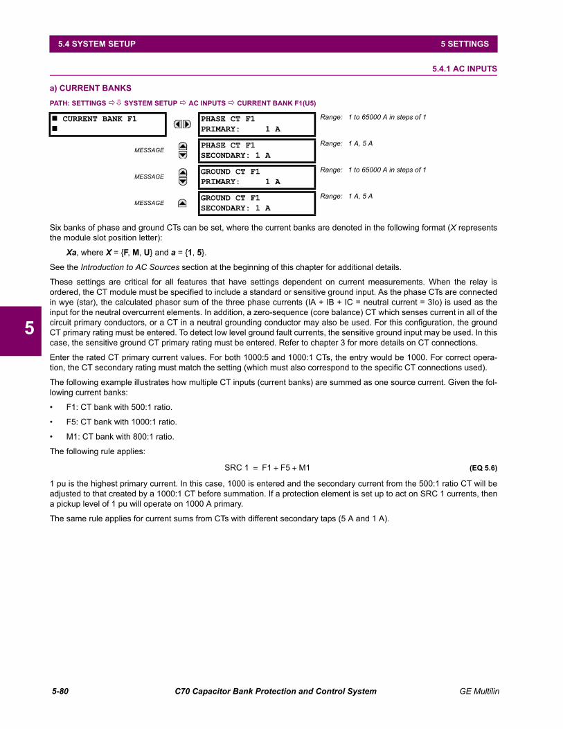
5-80 C70 Capacitor Bank Protection and Control System GE Multilin
5.4 SYSTEM SETUP 5 SETTINGS
5
5.4SYSTEM SETUP 5.4.1 AC INPUTS
a) CURRENT BANKS
PATH: SETTINGS SYSTEM SETUP AC INPUTS CURRENT BANK F1(U5)
Six banks of phase and ground CTs can be set, where the current banks are denoted in the following format (X representsthe module slot position letter):
Xa, where X = F, M, U and a = 1, 5.
See the Introduction to AC Sources section at the beginning of this chapter for additional details.
These settings are critical for all features that have settings dependent on current measurements. When the relay isordered, the CT module must be specified to include a standard or sensitive ground input. As the phase CTs are connectedin wye (star), the calculated phasor sum of the three phase currents (IA + IB + IC = neutral current = 3Io) is used as theinput for the neutral overcurrent elements. In addition, a zero-sequence (core balance) CT which senses current in all of thecircuit primary conductors, or a CT in a neutral grounding conductor may also be used. For this configuration, the groundCT primary rating must be entered. To detect low level ground fault currents, the sensitive ground input may be used. In thiscase, the sensitive ground CT primary rating must be entered. Refer to chapter 3 for more details on CT connections.
Enter the rated CT primary current values. For both 1000:5 and 1000:1 CTs, the entry would be 1000. For correct opera-tion, the CT secondary rating must match the setting (which must also correspond to the specific CT connections used).
The following example illustrates how multiple CT inputs (current banks) are summed as one source current. Given the fol-lowing current banks:
• F1: CT bank with 500:1 ratio.
• F5: CT bank with 1000:1 ratio.
• M1: CT bank with 800:1 ratio.
The following rule applies:
(EQ 5.6)
1 pu is the highest primary current. In this case, 1000 is entered and the secondary current from the 500:1 ratio CT will beadjusted to that created by a 1000:1 CT before summation. If a protection element is set up to act on SRC 1 currents, thena pickup level of 1 pu will operate on 1000 A primary.
The same rule applies for current sums from CTs with different secondary taps (5 A and 1 A).
CURRENT BANK F1
PHASE CT F1PRIMARY: 1 A
Range: 1 to 65000 A in steps of 1
MESSAGEPHASE CT F1SECONDARY: 1 A
Range: 1 A, 5 A
MESSAGEGROUND CT F1PRIMARY: 1 A
Range: 1 to 65000 A in steps of 1
MESSAGEGROUND CT F1SECONDARY: 1 A
Range: 1 A, 5 A
SRC 1 F1 F5 M1+ +=

GE Multilin C70 Capacitor Bank Protection and Control System 5-81
5 SETTINGS 5.4 SYSTEM SETUP
5
b) VOLTAGE BANKS
PATH: SETTINGS SYSTEM SETUP AC INPUTS VOLTAGE BANK F5(U5)
Three bank of phase/auxiliary VTs can be set, where voltage banks are denoted in the following format (X represents themodule slot position letter):
Xa, where X = F, M, U and a = 5.
See the Introduction to AC sources section at the beginning of this chapter for additional details.
With VTs installed, the relay can perform voltage measurements as well as power calculations. Enter the PHASE VT F5 CON-
NECTION made to the system as “Wye” or “Delta”. An open-delta source VT connection would be entered as “Delta”.
The nominal PHASE VT F5 SECONDARY voltage setting is the voltage across the relay input terminals when nominalvoltage is applied to the VT primary.
For example, on a system with a 13.8 kV nominal primary voltage and with a 14400:120 volt VT in a delta connec-tion, the secondary voltage would be 115; that is, (13800 / 14400) × 120. For a wye connection, the voltage valueentered must be the phase to neutral voltage which would be 115 = 66.4.
On a 14.4 kV system with a delta connection and a VT primary to secondary turns ratio of 14400:120, the voltagevalue entered would be 120; that is, 14400 / 120.
If the PHASE VT F5 CONNECTION is set to “Delta”, the relay will not calculate voltage harmonics.
5.4.2 POWER SYSTEM
PATH: SETTINGS SYSTEM SETUP POWER SYSTEM
The power system NOMINAL FREQUENCY value is used as a default to set the digital sampling rate if the system frequencycannot be measured from available signals. This may happen if the signals are not present or are heavily distorted. Beforereverting to the nominal frequency, the frequency tracking algorithm holds the last valid frequency measurement for a safeperiod of time while waiting for the signals to reappear or for the distortions to decay.
VOLTAGE BANK F5
PHASE VT F5CONNECTION: Wye
Range: Wye, Delta
MESSAGEPHASE VT F5SECONDARY: 66.4 V
Range: 25.0 to 240.0 V in steps of 0.1
MESSAGEPHASE VT F5RATIO: 1.00 :1
Range: 1.00 to 24000.00 in steps of 0.01
MESSAGEAUXILIARY VT F5CONNECTION: Vag
Range: Vn, Vag, Vbg, Vcg, Vab, Vbc, Vca
MESSAGEAUXILIARY VT F5SECONDARY: 66.4 V
Range: 25.0 to 240.0 V in steps of 0.1
MESSAGEAUXILIARY VT F5RATIO: 1.00 :1
Range: 1.00 to 24000.00 in steps of 0.01
POWER SYSTEM
NOMINAL FREQUENCY:60 Hz
Range: 25 to 60 Hz in steps of 1
MESSAGEPHASE ROTATION:ABC
Range: ABC, ACB
MESSAGEFREQUENCY AND PHASEREFERENCE: SRC 1
Range: SRC 1, SRC 2
MESSAGEFREQUENCY TRACKING:Enabled
Range: Disabled, Enabled
NOTE
3
NOTE
5-82 C70 Capacitor Bank Protection and Control System GE Multilin
5.4 SYSTEM SETUP 5 SETTINGS
5
The phase sequence of the power system is required to properly calculate sequence components and power parameters.The PHASE ROTATION setting matches the power system phase sequence. Note that this setting informs the relay of theactual system phase sequence, either ABC or ACB. CT and VT inputs on the relay, labeled as A, B, and C, must be con-nected to system phases A, B, and C for correct operation.
The FREQUENCY AND PHASE REFERENCE setting determines which signal source is used (and hence which AC signal) forphase angle reference. The AC signal used is prioritized based on the AC inputs that are configured for the signal source:phase voltages takes precedence, followed by auxiliary voltage, then phase currents, and finally ground current.
For three phase selection, phase A is used for angle referencing ( ), while Clarke transformation of thephase signals is used for frequency metering and tracking ( ) for better performance dur-ing fault, open pole, and VT and CT fail conditions.
The phase reference and frequency tracking AC signals are selected based upon the Source configuration, regardless ofwhether or not a particular signal is actually applied to the relay.
Phase angle of the reference signal will always display zero degrees and all other phase angles will be relative to this sig-nal. If the pre-selected reference signal is not measurable at a given time, the phase angles are not referenced.
The phase angle referencing is done via a phase locked loop, which can synchronize independent UR-series relays if theyhave the same AC signal reference. This results in very precise correlation of phase angle indications between differentUR-series relays.
FREQUENCY TRACKING is set to “Disabled” only in unusual circumstances; consult the factory for special variable-frequency applications.
The frequency tracking feature functions only when the C70 is in the “Programmed” mode. If the C70 is “Not Pro-grammed”, then metering values are available but can exhibit significant errors.
VANGLE REF VA=VFREQUENCY 2VA VB– VC– 3=
NOTE
NOTE

GE Multilin C70 Capacitor Bank Protection and Control System 5-83
5 SETTINGS 5.4 SYSTEM SETUP
5
5.4.3 SIGNAL SOURCES
PATH: SETTINGS SYSTEM SETUP SIGNAL SOURCES SOURCE 1(6)
Identical menus are available for each source. The "SRC 1" text can be replaced by with a user-defined name appropriatefor the associated source.
The first letter in the source identifier represents the module slot position. The number directly following this letter repre-sents either the first bank of four channels (1, 2, 3, 4) called “1” or the second bank of four channels (5, 6, 7, 8) called “5” ina particular CT/VT module. Refer to the Introduction to AC sources section at the beginning of this chapter for additionaldetails on this concept.
It is possible to select the sum of all CT combinations. The first channel displayed is the CT to which all others will bereferred. For example, the selection “F1+F5” indicates the sum of each phase from channels “F1” and “F5”, scaled towhichever CT has the higher ratio. Selecting “None” hides the associated actual values.
The approach used to configure the AC sources consists of several steps; first step is to specify the information about eachCT and VT input. For CT inputs, this is the nominal primary and secondary current. For VTs, this is the connection type,ratio and nominal secondary voltage. Once the inputs have been specified, the configuration for each source is entered,including specifying which CTs will be summed together.
User selection of AC parameters for comparator elements:
CT/VT modules automatically calculate all current and voltage parameters from the available inputs. Users must select thespecific input parameters to be measured by every element in the relevant settings menu. The internal design of the ele-ment specifies which type of parameter to use and provides a setting for source selection. In elements where the parametermay be either fundamental or RMS magnitude, such as phase time overcurrent, two settings are provided. One settingspecifies the source, the second setting selects between fundamental phasor and RMS.
AC input actual values:
The calculated parameters associated with the configured voltage and current inputs are displayed in the current and volt-age sections of actual values. Only the phasor quantities associated with the actual AC physical input channels will be dis-played here. All parameters contained within a configured source are displayed in the sources section of the actual values.
Disturbance detectors (internal):
The disturbance detector (ANSI 50DD) element is a sensitive current disturbance detector that detects any disturbance onthe protected system. The 50DD function is intended for use in conjunction with measuring elements, blocking of currentbased elements (to prevent maloperation as a result of the wrong settings), and starting oscillography data capture. A dis-turbance detector is provided for each source.
The 50DD function responds to the changes in magnitude of the sequence currents. The disturbance detector schemelogic is as follows:
SOURCE 1
SOURCE 1 NAME:SRC 1
Range: up to six alphanumeric characters
MESSAGESOURCE 1 PHASE CT:None
Range: None, F1, F5, F1+F5,... up to a combination ofany 6 CTs. Only Phase CT inputs are displayed.
MESSAGESOURCE 1 GROUND CT:None
Range: None, F1, F5, F1+F5,... up to a combination ofany 6 CTs. Only Ground CT inputs are displayed.
MESSAGESOURCE 1 PHASE VT:None
Range: None, F5, M5, U5Only phase voltage inputs will be displayed.
MESSAGESOURCE 1 AUX VT:None
Range: None, F5, M5, U5Only auxiliary voltage inputs will be displayed.

5-84 C70 Capacitor Bank Protection and Control System GE Multilin
5.4 SYSTEM SETUP 5 SETTINGS
5
Figure 5–21: DISTURBANCE DETECTOR LOGIC DIAGRAM
The disturbance detector responds to the change in currents of twice the current cut-off level. The default cut-off thresholdis 0.02 pu; thus by default the disturbance detector responds to a change of 0.04 pu. The metering sensitivity setting (PROD-
UCT SETUP DISPLAY PROPERTIES CURRENT CUT-OFF LEVEL) controls the sensitivity of the disturbance detectoraccordingly.
Example use of sources:
An example of the use of sources is shown in the diagram below. A relay could have the following hardware configuration:
This configuration could be used on a two-winding transformer, with one winding connected into a breaker-and-a-half sys-tem. The following figure shows the arrangement of sources used to provide the functions required in this application, andthe CT/VT inputs that are used to provide the data.
Figure 5–22: EXAMPLE USE OF SOURCES
INCREASING SLOT POSITION LETTER -->
CT/VT MODULE 1 CT/VT MODULE 2 CT/VT MODULE 3
8 CTs 4 CTs, 4 VTs 4 CTs, 4 VTs
827092A3.CDR
SOURCE 1CURRENT PHASOR
PRODUCT SETUP/DISPLAYPROPERTIES/CURRENTCUT-OFF LEVEL
PRODUCT SETUP/DISPLAYPROPERTIES/CURRENTCUT-OFF LEVEL
PRODUCT SETUP/DISPLAYPROPERTIES/CURRENTCUT-OFF LEVEL
SOURCE 2CURRENT PHASOR
SOURCE 6CURRENT PHASOR
ACTUAL
SETTING
SETTING
SETTING
ACTUAL
ACTUAL
FLEXLOGIC OPERAND
FLEXLOGIC OPERAND
FLEXLOGIC OPERAND
I_1
I_1
I_1
SRC 1 50DD OP
SRC 2 50DD OP
SRC 6 50DD OP
I_2
I_2
I_2
I_0
I_0
I_0
OR
OR
OR
Where ’ is 2 cycles oldI
Where ’ is 2 cycles oldI
Where ’ is 2 cycles oldI
I I_1 - _1’ >2*CUT-OFF
I I_1 - _1’ >2*CUT-OFF
I I_1 - _1’ >2*CUT-OFF
I I_2 - _2’ >2*CUT-OFF
I I_2 - _2’ >2*CUT-OFF
I I_2 - _2’ >2*CUT-OFF
I I_0 - _0’ >2*CUT-OFF
I I_0 - _0’ >2*CUT-OFF
I I_0 - _0’ >2*CUT-OFF
F 5
F 1 DSP Bank
U 1
M 1
M 1
M 5
51BF-1 51BF-2
Source 4
87T
51P
UR Relay
A
V
V
A
W
W
Var
Var
Amps
Source 1
Source 3
Volts Amps
AmpsVolts
Amps
Source 2
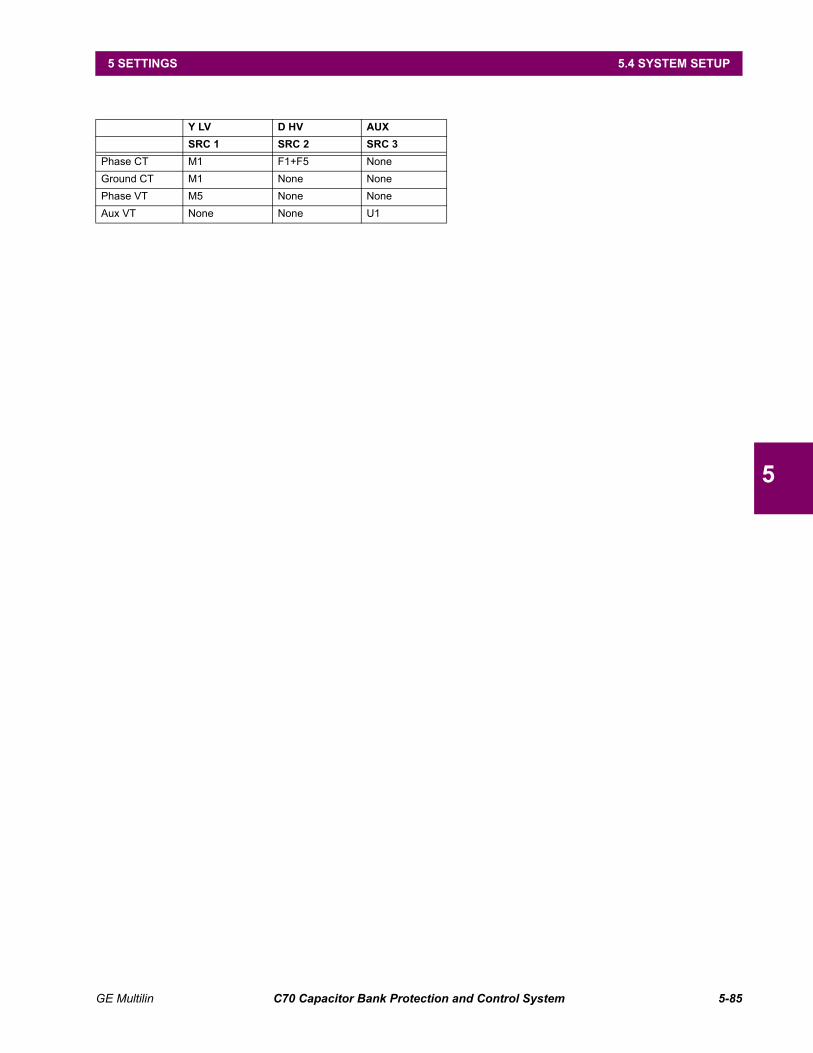
GE Multilin C70 Capacitor Bank Protection and Control System 5-85
5 SETTINGS 5.4 SYSTEM SETUP
5
Y LV D HV AUX
SRC 1 SRC 2 SRC 3
Phase CT M1 F1+F5 None
Ground CT M1 None None
Phase VT M5 None None
Aux VT None None U1
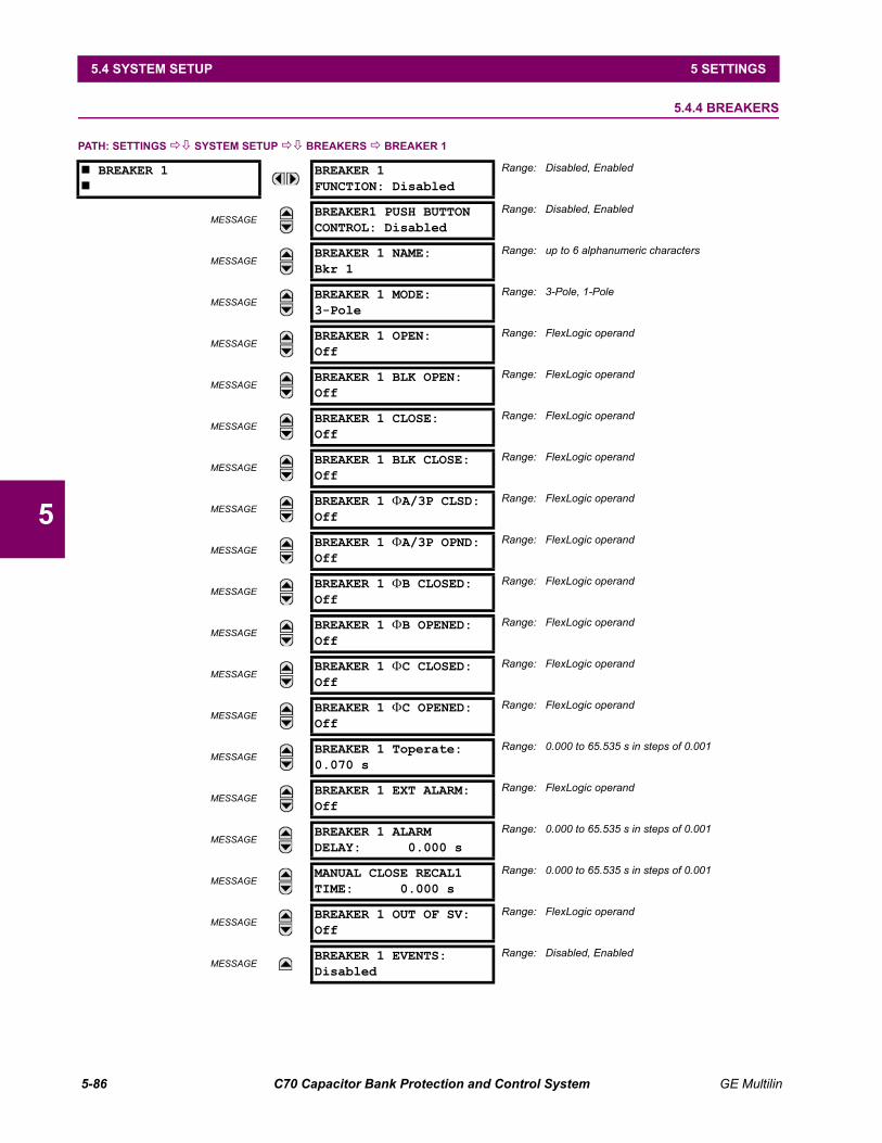
5-86 C70 Capacitor Bank Protection and Control System GE Multilin
5.4 SYSTEM SETUP 5 SETTINGS
5
5.4.4 BREAKERS
PATH: SETTINGS SYSTEM SETUP BREAKERS BREAKER 1
BREAKER 1
BREAKER 1FUNCTION: Disabled
Range: Disabled, Enabled
MESSAGEBREAKER1 PUSH BUTTONCONTROL: Disabled
Range: Disabled, Enabled
MESSAGEBREAKER 1 NAME:Bkr 1
Range: up to 6 alphanumeric characters
MESSAGEBREAKER 1 MODE:3-Pole
Range: 3-Pole, 1-Pole
MESSAGEBREAKER 1 OPEN:Off
Range: FlexLogic operand
MESSAGEBREAKER 1 BLK OPEN:Off
Range: FlexLogic operand
MESSAGEBREAKER 1 CLOSE:Off
Range: FlexLogic operand
MESSAGEBREAKER 1 BLK CLOSE:Off
Range: FlexLogic operand
MESSAGEBREAKER 1 A/3P CLSD:Off
Range: FlexLogic operand
MESSAGEBREAKER 1 A/3P OPND:Off
Range: FlexLogic operand
MESSAGEBREAKER 1 B CLOSED:Off
Range: FlexLogic operand
MESSAGEBREAKER 1 B OPENED:Off
Range: FlexLogic operand
MESSAGEBREAKER 1 C CLOSED:Off
Range: FlexLogic operand
MESSAGEBREAKER 1 C OPENED:Off
Range: FlexLogic operand
MESSAGEBREAKER 1 Toperate:0.070 s
Range: 0.000 to 65.535 s in steps of 0.001
MESSAGEBREAKER 1 EXT ALARM:Off
Range: FlexLogic operand
MESSAGEBREAKER 1 ALARMDELAY: 0.000 s
Range: 0.000 to 65.535 s in steps of 0.001
MESSAGEMANUAL CLOSE RECAL1TIME: 0.000 s
Range: 0.000 to 65.535 s in steps of 0.001
MESSAGEBREAKER 1 OUT OF SV:Off
Range: FlexLogic operand
MESSAGEBREAKER 1 EVENTS:Disabled
Range: Disabled, Enabled
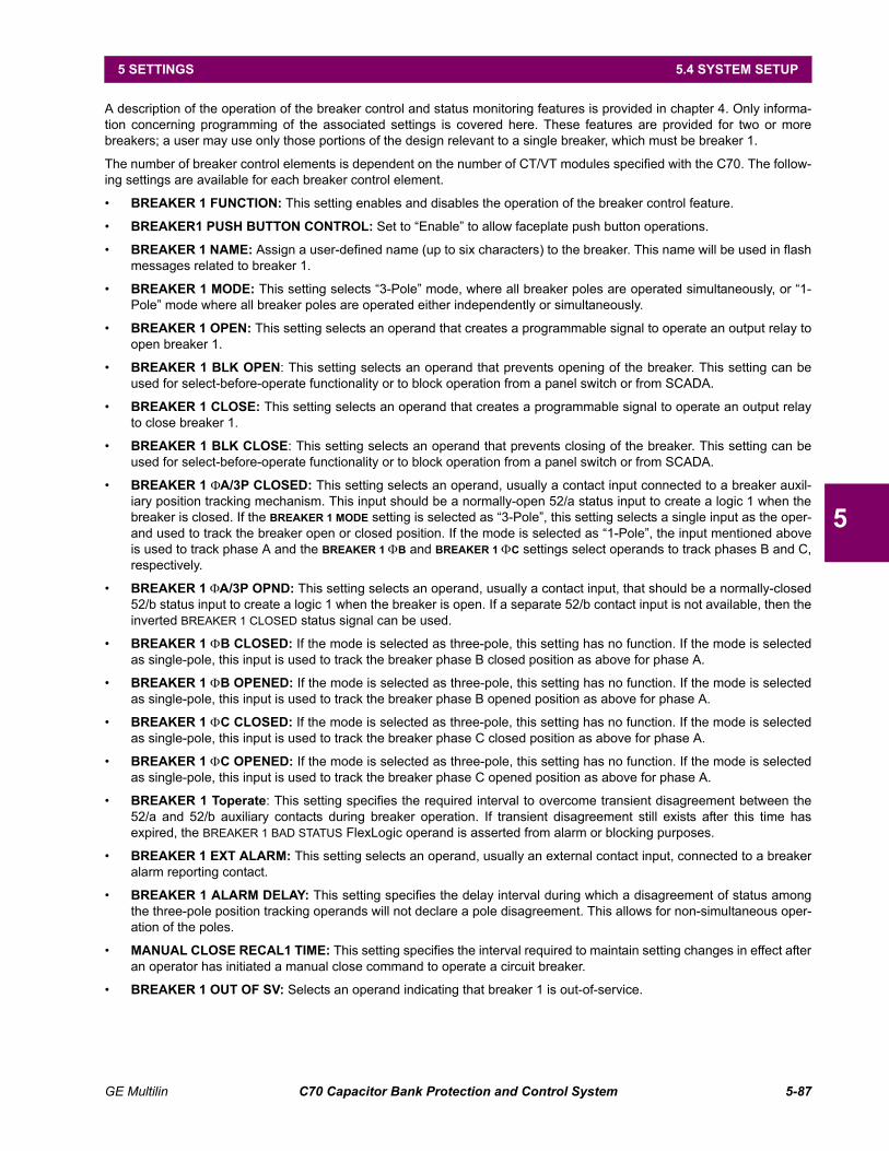
GE Multilin C70 Capacitor Bank Protection and Control System 5-87
5 SETTINGS 5.4 SYSTEM SETUP
5
A description of the operation of the breaker control and status monitoring features is provided in chapter 4. Only informa-tion concerning programming of the associated settings is covered here. These features are provided for two or morebreakers; a user may use only those portions of the design relevant to a single breaker, which must be breaker 1.
The number of breaker control elements is dependent on the number of CT/VT modules specified with the C70. The follow-ing settings are available for each breaker control element.
• BREAKER 1 FUNCTION: This setting enables and disables the operation of the breaker control feature.
• BREAKER1 PUSH BUTTON CONTROL: Set to “Enable” to allow faceplate push button operations.
• BREAKER 1 NAME: Assign a user-defined name (up to six characters) to the breaker. This name will be used in flashmessages related to breaker 1.
• BREAKER 1 MODE: This setting selects “3-Pole” mode, where all breaker poles are operated simultaneously, or “1-Pole” mode where all breaker poles are operated either independently or simultaneously.
• BREAKER 1 OPEN: This setting selects an operand that creates a programmable signal to operate an output relay toopen breaker 1.
• BREAKER 1 BLK OPEN: This setting selects an operand that prevents opening of the breaker. This setting can beused for select-before-operate functionality or to block operation from a panel switch or from SCADA.
• BREAKER 1 CLOSE: This setting selects an operand that creates a programmable signal to operate an output relayto close breaker 1.
• BREAKER 1 BLK CLOSE: This setting selects an operand that prevents closing of the breaker. This setting can beused for select-before-operate functionality or to block operation from a panel switch or from SCADA.
• BREAKER 1 A/3P CLOSED: This setting selects an operand, usually a contact input connected to a breaker auxil-iary position tracking mechanism. This input should be a normally-open 52/a status input to create a logic 1 when thebreaker is closed. If the BREAKER 1 MODE setting is selected as “3-Pole”, this setting selects a single input as the oper-and used to track the breaker open or closed position. If the mode is selected as “1-Pole”, the input mentioned aboveis used to track phase A and the BREAKER 1 B and BREAKER 1 C settings select operands to track phases B and C,respectively.
• BREAKER 1 A/3P OPND: This setting selects an operand, usually a contact input, that should be a normally-closed52/b status input to create a logic 1 when the breaker is open. If a separate 52/b contact input is not available, then theinverted BREAKER 1 CLOSED status signal can be used.
• BREAKER 1 B CLOSED: If the mode is selected as three-pole, this setting has no function. If the mode is selectedas single-pole, this input is used to track the breaker phase B closed position as above for phase A.
• BREAKER 1 B OPENED: If the mode is selected as three-pole, this setting has no function. If the mode is selectedas single-pole, this input is used to track the breaker phase B opened position as above for phase A.
• BREAKER 1 C CLOSED: If the mode is selected as three-pole, this setting has no function. If the mode is selectedas single-pole, this input is used to track the breaker phase C closed position as above for phase A.
• BREAKER 1 C OPENED: If the mode is selected as three-pole, this setting has no function. If the mode is selectedas single-pole, this input is used to track the breaker phase C opened position as above for phase A.
• BREAKER 1 Toperate: This setting specifies the required interval to overcome transient disagreement between the52/a and 52/b auxiliary contacts during breaker operation. If transient disagreement still exists after this time hasexpired, the BREAKER 1 BAD STATUS FlexLogic operand is asserted from alarm or blocking purposes.
• BREAKER 1 EXT ALARM: This setting selects an operand, usually an external contact input, connected to a breakeralarm reporting contact.
• BREAKER 1 ALARM DELAY: This setting specifies the delay interval during which a disagreement of status amongthe three-pole position tracking operands will not declare a pole disagreement. This allows for non-simultaneous oper-ation of the poles.
• MANUAL CLOSE RECAL1 TIME: This setting specifies the interval required to maintain setting changes in effect afteran operator has initiated a manual close command to operate a circuit breaker.
• BREAKER 1 OUT OF SV: Selects an operand indicating that breaker 1 is out-of-service.

5-88 C70 Capacitor Bank Protection and Control System GE Multilin
5.4 SYSTEM SETUP 5 SETTINGS
5
Figure 5–23: DUAL BREAKER CONTROL SCHEME LOGIC (Sheet 1 of 2)
IEC 61850 functionality is permitted when the C70 is in “Programmed” mode and not in the local control mode.
NOTE
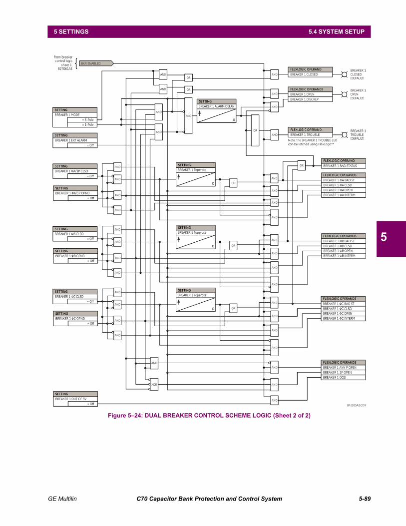
GE Multilin C70 Capacitor Bank Protection and Control System 5-89
5 SETTINGS 5.4 SYSTEM SETUP
5
Figure 5–24: DUAL BREAKER CONTROL SCHEME LOGIC (Sheet 2 of 2)

5-90 C70 Capacitor Bank Protection and Control System GE Multilin
5.4 SYSTEM SETUP 5 SETTINGS
5
5.4.5 DISCONNECT SWITCHES
PATH: SETTINGS SYSTEM SETUP SWITCHES SWITCH 1
The disconnect switch element contains the auxiliary logic for status and serves as the interface for opening and closing ofdisconnect switches from SCADA or through the front panel interface. The disconnect switch element can be used to cre-ate an interlocking functionality. For greater security in determination of the switch pole position, both the 89/a and 89/bauxiliary contacts are used with reporting of the discrepancy between them. The number of available disconnect switchesdepends on the number of the CT/VT modules ordered with the C70.
• SWITCH 1 FUNCTION: This setting enables and disables the operation of the disconnect switch element.
• SWITCH 1 NAME: Assign a user-defined name (up to six characters) to the disconnect switch. This name will be usedin flash messages related to disconnect switch 1.
• SWITCH 1 MODE: This setting selects “3-Pole” mode, where disconnect switch poles have a single common auxiliaryswitch, or “1-Pole” mode where each disconnect switch pole has its own auxiliary switch.
SWITCH 1
SWITCH 1FUNCTION: Disabled
Range: Disabled, Enabled
MESSAGESWITCH 1 NAME:SW 1
Range: up to 6 alphanumeric characters
MESSAGESWITCH 1 MODE:3-Pole
Range: 3-Pole, 1-Pole
MESSAGESWITCH 1 OPEN:Off
Range: FlexLogic operand
MESSAGESWITCH 1 BLK OPEN:Off
Range: FlexLogic operand
MESSAGESWITCH 1 CLOSE:Off
Range: FlexLogic operand
MESSAGESWITCH 1 BLK CLOSE:Off
Range: FlexLogic operand
MESSAGESWTCH 1 A/3P CLSD:Off
Range: FlexLogic operand
MESSAGESWTCH 1 A/3P OPND:Off
Range: FlexLogic operand
MESSAGESWITCH 1 B CLOSED:Off
Range: FlexLogic operand
MESSAGESWITCH 1 B OPENED:Off
Range: FlexLogic operand
MESSAGESWITCH 1 C CLOSED:Off
Range: FlexLogic operand
MESSAGESWITCH 1 C OPENED:Off
Range: FlexLogic operand
MESSAGESWITCH 1 Toperate:0.070 s
Range: 0.000 to 65.535 s in steps of 0.001
MESSAGESWITCH 1 ALARMDELAY: 0.000 s
Range: 0.000 to 65.535 s in steps of 0.001
MESSAGESWITCH 1 EVENTS:Disabled
Range: Disabled, Enabled
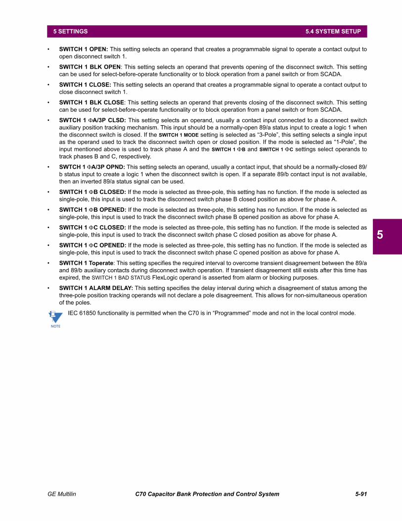
GE Multilin C70 Capacitor Bank Protection and Control System 5-91
5 SETTINGS 5.4 SYSTEM SETUP
5
• SWITCH 1 OPEN: This setting selects an operand that creates a programmable signal to operate a contact output toopen disconnect switch 1.
• SWITCH 1 BLK OPEN: This setting selects an operand that prevents opening of the disconnect switch. This settingcan be used for select-before-operate functionality or to block operation from a panel switch or from SCADA.
• SWITCH 1 CLOSE: This setting selects an operand that creates a programmable signal to operate a contact output toclose disconnect switch 1.
• SWITCH 1 BLK CLOSE: This setting selects an operand that prevents closing of the disconnect switch. This settingcan be used for select-before-operate functionality or to block operation from a panel switch or from SCADA.
• SWTCH 1 A/3P CLSD: This setting selects an operand, usually a contact input connected to a disconnect switchauxiliary position tracking mechanism. This input should be a normally-open 89/a status input to create a logic 1 whenthe disconnect switch is closed. If the SWITCH 1 MODE setting is selected as “3-Pole”, this setting selects a single inputas the operand used to track the disconnect switch open or closed position. If the mode is selected as “1-Pole”, theinput mentioned above is used to track phase A and the SWITCH 1 B and SWITCH 1 C settings select operands totrack phases B and C, respectively.
• SWTCH 1 A/3P OPND: This setting selects an operand, usually a contact input, that should be a normally-closed 89/b status input to create a logic 1 when the disconnect switch is open. If a separate 89/b contact input is not available,then an inverted 89/a status signal can be used.
• SWITCH 1 B CLOSED: If the mode is selected as three-pole, this setting has no function. If the mode is selected assingle-pole, this input is used to track the disconnect switch phase B closed position as above for phase A.
• SWITCH 1 B OPENED: If the mode is selected as three-pole, this setting has no function. If the mode is selected assingle-pole, this input is used to track the disconnect switch phase B opened position as above for phase A.
• SWITCH 1 C CLOSED: If the mode is selected as three-pole, this setting has no function. If the mode is selected assingle-pole, this input is used to track the disconnect switch phase C closed position as above for phase A.
• SWITCH 1 C OPENED: If the mode is selected as three-pole, this setting has no function. If the mode is selected assingle-pole, this input is used to track the disconnect switch phase C opened position as above for phase A.
• SWITCH 1 Toperate: This setting specifies the required interval to overcome transient disagreement between the 89/aand 89/b auxiliary contacts during disconnect switch operation. If transient disagreement still exists after this time hasexpired, the SWITCH 1 BAD STATUS FlexLogic operand is asserted from alarm or blocking purposes.
• SWITCH 1 ALARM DELAY: This setting specifies the delay interval during which a disagreement of status among thethree-pole position tracking operands will not declare a pole disagreement. This allows for non-simultaneous operationof the poles.
IEC 61850 functionality is permitted when the C70 is in “Programmed” mode and not in the local control mode.
NOTE
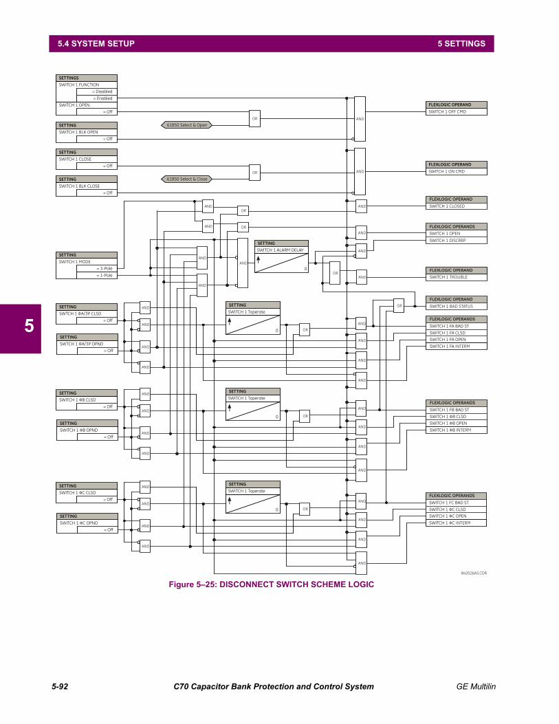
5-92 C70 Capacitor Bank Protection and Control System GE Multilin
5.4 SYSTEM SETUP 5 SETTINGS
5
Figure 5–25: DISCONNECT SWITCH SCHEME LOGIC

GE Multilin C70 Capacitor Bank Protection and Control System 5-93
5 SETTINGS 5.4 SYSTEM SETUP
5
5.4.6 FLEXCURVES
a) SETTINGS
PATH: SETTINGS SYSTEM SETUP FLEXCURVES FLEXCURVE A(D)
FlexCurves A through D have settings for entering times to reset and operate at the following pickup levels: 0.00 to 0.98and 1.03 to 20.00. This data is converted into two continuous curves by linear interpolation between data points. To enter acustom FlexCurve, enter the reset and operate times (using the VALUE keys) for each selected pickup point (using theMESSAGE UP/DOWN keys) for the desired protection curve (A, B, C, or D).
The relay using a given FlexCurve applies linear approximation for times between the user-entered points. Specialcare must be applied when setting the two points that are close to the multiple of pickup of 1; that is, 0.98 pu and1.03 pu. It is recommended to set the two times to a similar value; otherwise, the linear approximation may result inundesired behavior for the operating quantity that is close to 1.00 pu.
FLEXCURVE A
FLEXCURVE A TIME AT0.00 xPKP: 0 ms
Range: 0 to 65535 ms in steps of 1
Table 5–6: FLEXCURVE TABLE
RESET TIMEMS
RESET TIMEMS
OPERATE TIMEMS
OPERATE TIMEMS
OPERATE TIMEMS
OPERATE TIMEMS
0.00 0.68 1.03 2.9 4.9 10.5
0.05 0.70 1.05 3.0 5.0 11.0
0.10 0.72 1.1 3.1 5.1 11.5
0.15 0.74 1.2 3.2 5.2 12.0
0.20 0.76 1.3 3.3 5.3 12.5
0.25 0.78 1.4 3.4 5.4 13.0
0.30 0.80 1.5 3.5 5.5 13.5
0.35 0.82 1.6 3.6 5.6 14.0
0.40 0.84 1.7 3.7 5.7 14.5
0.45 0.86 1.8 3.8 5.8 15.0
0.48 0.88 1.9 3.9 5.9 15.5
0.50 0.90 2.0 4.0 6.0 16.0
0.52 0.91 2.1 4.1 6.5 16.5
0.54 0.92 2.2 4.2 7.0 17.0
0.56 0.93 2.3 4.3 7.5 17.5
0.58 0.94 2.4 4.4 8.0 18.0
0.60 0.95 2.5 4.5 8.5 18.5
0.62 0.96 2.6 4.6 9.0 19.0
0.64 0.97 2.7 4.7 9.5 19.5
0.66 0.98 2.8 4.8 10.0 20.0
NOTE

5-94 C70 Capacitor Bank Protection and Control System GE Multilin
5.4 SYSTEM SETUP 5 SETTINGS
5
b) FLEXCURVE CONFIGURATION WITH ENERVISTA UR SETUP
The EnerVista UR Setup software allows for easy configuration and management of FlexCurves and their associated datapoints. Prospective FlexCurves can be configured from a selection of standard curves to provide the best approximate fit,then specific data points can be edited afterwards. Alternately, curve data can be imported from a specified file (.csv format)by selecting the Import Data From EnerVista UR Setup setting.
Curves and data can be exported, viewed, and cleared by clicking the appropriate buttons. FlexCurves are customized byediting the operating time (ms) values at pre-defined per-unit current multiples. Note that the pickup multiples start at zero(implying the "reset time"), operating time below pickup, and operating time above pickup.
c) RECLOSER CURVE EDITING
Recloser curve selection is special in that recloser curves can be shaped into a composite curve with a minimum responsetime and a fixed time above a specified pickup multiples. There are 41 recloser curve types supported. These definite oper-ating times are useful to coordinate operating times, typically at higher currents and where upstream and downstream pro-tective devices have different operating characteristics. The recloser curve configuration window shown below appearswhen the Initialize From EnerVista UR Setup setting is set to “Recloser Curve” and the Initialize FlexCurve button isclicked.
Figure 5–26: RECLOSER CURVE INITIALIZATION
The multiplier and adder settings only affect the curve portion of the characteristic and not the MRT and HCT set-tings. The HCT settings override the MRT settings for multiples of pickup greater than the HCT ratio.
842721A1.CDR
Multiplier: Scales (multiplies) the curve operating times
Addr: Adds the time specified in this field (in ms) to eachoperating time value.curve
Minimum Response Time (MRT): If enabled, the MRT settingdefines the shortest operating time even if the curve suggestsa shorter time at higher current multiples. A composite operatingcharacteristic is effectively defined. For current multiples lowerthan the intersection point, the curve dictates the operating time;otherwise, the MRT does. An information message appearswhen attempting to apply an MRT shorter than the minimumcurve time.
High Current Time:
HCT Ratio
HCT
Allows the user to set a pickup multiplefrom which point onwards the operating time is fixed. This isnormally only required at higher current levels. Thedefines the high current pickup multiple; the defines theoperating time.
NOTE

GE Multilin C70 Capacitor Bank Protection and Control System 5-95
5 SETTINGS 5.4 SYSTEM SETUP
5
d) EXAMPLE
A composite curve can be created from the GE_111 standard with MRT = 200 ms and HCT initially disabled and thenenabled at eight (8) times pickup with an operating time of 30 ms. At approximately four (4) times pickup, the curve operat-ing time is equal to the MRT and from then onwards the operating time remains at 200 ms (see below).
Figure 5–27: COMPOSITE RECLOSER CURVE WITH HCT DISABLED
With the HCT feature enabled, the operating time reduces to 30 ms for pickup multiples exceeding 8 times pickup.
Figure 5–28: COMPOSITE RECLOSER CURVE WITH HCT ENABLED
Configuring a composite curve with an increase in operating time at increased pickup multiples is not allowed. If thisis attempted, the EnerVista UR Setup software generates an error message and discards the proposed changes.
e) STANDARD RECLOSER CURVES
The standard recloser curves available for the C70 are displayed in the following graphs.
842719A1.CDR
842720A1.CDR
NOTE

5-96 C70 Capacitor Bank Protection and Control System GE Multilin
5.4 SYSTEM SETUP 5 SETTINGS
5Figure 5–29: RECLOSER CURVES GE101 TO GE106
Figure 5–30: RECLOSER CURVES GE113, GE120, GE138 AND GE142
GE104
1 1.2 1.5 2 2.5 3 4 5 6 7 8 9 10 12 15 20
0.01
0.02
0.05
0.1
0.2
0.5
1
2
CURRENT (multiple of pickup)
TIM
E (s
ec)
GE101 GE102
GE103
GE106
GE105
842723A1.CDR
1 1.2 1.5 2 2.5 3 4 5 6 7 8 9 10 12 15 200.05
0.1
0.2
0.5
1
2
5
10
20
50
CURRENT (multiple of pickup)
TIM
E (s
ec)
GE113
GE142
GE138
GE120
842725A1.CDR

GE Multilin C70 Capacitor Bank Protection and Control System 5-97
5 SETTINGS 5.4 SYSTEM SETUP
5Figure 5–31: RECLOSER CURVES GE134, GE137, GE140, GE151 AND GE201
Figure 5–32: RECLOSER CURVES GE131, GE141, GE152, AND GE200
1 1.2 1.5 2 2.5 3 4 5 6 7 8 9 10 12 15 20
0.5
1
2
5
10
20
50
CURRENT (multiple of pickup)
TIM
E (s
ec)
GE134
GE151
GE140
GE137
GE201
842730A1.CDR
1 1.2 1.5 2 2.5 3 4 5 6 7 8 9 10 12 15 202
5
10
20
50
CURRENT (multiple of pickup)
TIM
E (s
ec)
GE131
GE200
GE152
GE141
842728A1.CDR

5-98 C70 Capacitor Bank Protection and Control System GE Multilin
5.4 SYSTEM SETUP 5 SETTINGS
5 Figure 5–33: RECLOSER CURVES GE133, GE161, GE162, GE163, GE164 AND GE165
Figure 5–34: RECLOSER CURVES GE116, GE117, GE118, GE132, GE136, AND GE139
842729A1.CDR
1 1.2 1.5 2 2.5 3 4 5 6 7 8 9 10 12 15 200.01
0.02
0.05
0.1
0.2
0.5
1
2
5
10
20
50
CURRENT (multiple of pickup)
TIM
E (s
ec)
GE133
GE163
GE162
GE161
GE165
GE164
842726A1.CDR
1 1.2 1.5 2 2.5 3 4 5 6 7 8 9 10 12 15 200.01
0.02
0.05
0.1
0.2
0.5
1
2
5
10
20
CURRENT (multiple of pickup)
TIM
E (s
ec)
GE116
GE132
GE118 GE117
GE139
GE136
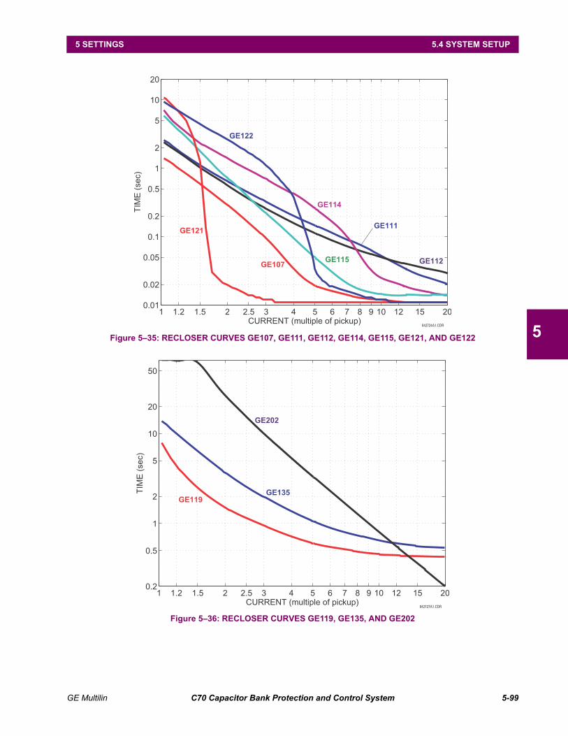
GE Multilin C70 Capacitor Bank Protection and Control System 5-99
5 SETTINGS 5.4 SYSTEM SETUP
5Figure 5–35: RECLOSER CURVES GE107, GE111, GE112, GE114, GE115, GE121, AND GE122
Figure 5–36: RECLOSER CURVES GE119, GE135, AND GE202
842724A1.CDR
1 1.2 1.5 2 2.5 3 4 5 6 7 8 9 10 12 15 200.01
0.02
0.05
0.1
0.2
0.5
1
2
5
10
20
CURRENT (multiple of pickup)
TIM
E (s
ec)
GE121
GE114
GE112
GE122
GE107 GE115
GE111
842727A1.CDR
1 1.2 1.5 2 2.5 3 4 5 6 7 8 9 10 12 15 200.2
0.5
1
2
5
10
20
50
CURRENT (multiple of pickup)
TIM
E (s
ec)
GE119
GE202
GE135

5-100 C70 Capacitor Bank Protection and Control System GE Multilin
5.5 FLEXLOGIC 5 SETTINGS
5
5.5FLEXLOGIC 5.5.1 INTRODUCTION TO FLEXLOGIC
To provide maximum flexibility to the user, the arrangement of internal digital logic combines fixed and user-programmedparameters. Logic upon which individual features are designed is fixed, and all other logic, from digital input signals throughelements or combinations of elements to digital outputs, is variable. The user has complete control of all variable logicthrough FlexLogic. In general, the system receives analog and digital inputs which it uses to produce analog and digital out-puts. The major sub-systems of a generic UR-series relay involved in this process are shown below.
Figure 5–37: UR ARCHITECTURE OVERVIEW
The states of all digital signals used in the C70 are represented by flags (or FlexLogic operands, which are described laterin this section). A digital “1” is represented by a 'set' flag. Any external contact change-of-state can be used to block an ele-ment from operating, as an input to a control feature in a FlexLogic equation, or to operate a contact output. The state of thecontact input can be displayed locally or viewed remotely via the communications facilities provided. If a simple schemewhere a contact input is used to block an element is desired, this selection is made when programming the element. Thiscapability also applies to the other features that set flags: elements, virtual inputs, remote inputs, schemes, and humanoperators.
If more complex logic than presented above is required, it is implemented via FlexLogic. For example, if it is desired to havethe closed state of contact input H7a and the operated state of the phase undervoltage element block the operation of thephase time overcurrent element, the two control input states are programmed in a FlexLogic equation. This equation ANDsthe two control inputs to produce a virtual output which is then selected when programming the phase time overcurrent tobe used as a blocking input. Virtual outputs can only be created by FlexLogic equations.
Traditionally, protective relay logic has been relatively limited. Any unusual applications involving interlocks, blocking, orsupervisory functions had to be hard-wired using contact inputs and outputs. FlexLogic minimizes the requirement for aux-iliary components and wiring while making more complex schemes possible.
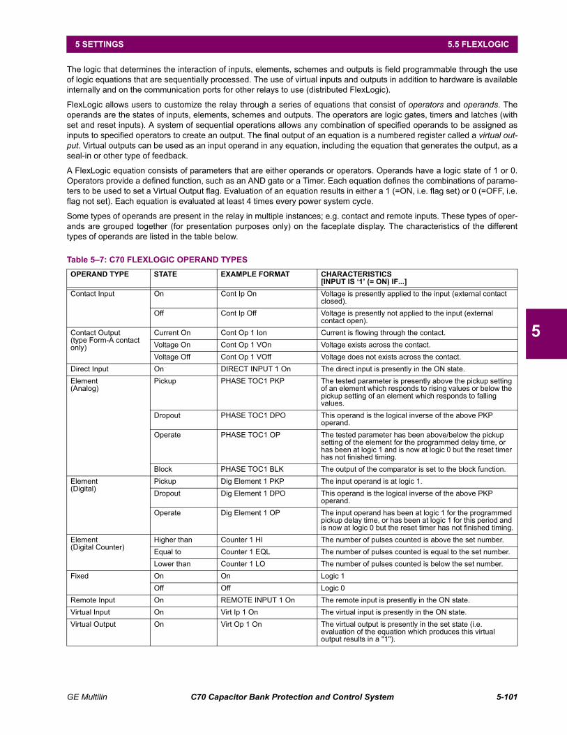
GE Multilin C70 Capacitor Bank Protection and Control System 5-101
5 SETTINGS 5.5 FLEXLOGIC
5
The logic that determines the interaction of inputs, elements, schemes and outputs is field programmable through the useof logic equations that are sequentially processed. The use of virtual inputs and outputs in addition to hardware is availableinternally and on the communication ports for other relays to use (distributed FlexLogic).
FlexLogic allows users to customize the relay through a series of equations that consist of operators and operands. Theoperands are the states of inputs, elements, schemes and outputs. The operators are logic gates, timers and latches (withset and reset inputs). A system of sequential operations allows any combination of specified operands to be assigned asinputs to specified operators to create an output. The final output of an equation is a numbered register called a virtual out-put. Virtual outputs can be used as an input operand in any equation, including the equation that generates the output, as aseal-in or other type of feedback.
A FlexLogic equation consists of parameters that are either operands or operators. Operands have a logic state of 1 or 0.Operators provide a defined function, such as an AND gate or a Timer. Each equation defines the combinations of parame-ters to be used to set a Virtual Output flag. Evaluation of an equation results in either a 1 (=ON, i.e. flag set) or 0 (=OFF, i.e.flag not set). Each equation is evaluated at least 4 times every power system cycle.
Some types of operands are present in the relay in multiple instances; e.g. contact and remote inputs. These types of oper-ands are grouped together (for presentation purposes only) on the faceplate display. The characteristics of the differenttypes of operands are listed in the table below.
Table 5–7: C70 FLEXLOGIC OPERAND TYPES
OPERAND TYPE STATE EXAMPLE FORMAT CHARACTERISTICS[INPUT IS ‘1’ (= ON) IF...]
Contact Input On Cont Ip On Voltage is presently applied to the input (external contact closed).
Off Cont Ip Off Voltage is presently not applied to the input (external contact open).
Contact Output(type Form-A contact only)
Current On Cont Op 1 Ion Current is flowing through the contact.
Voltage On Cont Op 1 VOn Voltage exists across the contact.
Voltage Off Cont Op 1 VOff Voltage does not exists across the contact.
Direct Input On DIRECT INPUT 1 On The direct input is presently in the ON state.
Element(Analog)
Pickup PHASE TOC1 PKP The tested parameter is presently above the pickup setting of an element which responds to rising values or below the pickup setting of an element which responds to falling values.
Dropout PHASE TOC1 DPO This operand is the logical inverse of the above PKP operand.
Operate PHASE TOC1 OP The tested parameter has been above/below the pickup setting of the element for the programmed delay time, or has been at logic 1 and is now at logic 0 but the reset timer has not finished timing.
Block PHASE TOC1 BLK The output of the comparator is set to the block function.
Element(Digital)
Pickup Dig Element 1 PKP The input operand is at logic 1.
Dropout Dig Element 1 DPO This operand is the logical inverse of the above PKP operand.
Operate Dig Element 1 OP The input operand has been at logic 1 for the programmed pickup delay time, or has been at logic 1 for this period and is now at logic 0 but the reset timer has not finished timing.
Element(Digital Counter)
Higher than Counter 1 HI The number of pulses counted is above the set number.
Equal to Counter 1 EQL The number of pulses counted is equal to the set number.
Lower than Counter 1 LO The number of pulses counted is below the set number.
Fixed On On Logic 1
Off Off Logic 0
Remote Input On REMOTE INPUT 1 On The remote input is presently in the ON state.
Virtual Input On Virt Ip 1 On The virtual input is presently in the ON state.
Virtual Output On Virt Op 1 On The virtual output is presently in the set state (i.e. evaluation of the equation which produces this virtual output results in a "1").

5-102 C70 Capacitor Bank Protection and Control System GE Multilin
5.5 FLEXLOGIC 5 SETTINGS
5
The operands available for this relay are listed alphabetically by types in the following table.
Table 5–8: C70 FLEXLOGIC OPERANDS (Sheet 1 of 9)
OPERAND TYPE OPERAND SYNTAX OPERAND DESCRIPTION
CONTROL PUSHBUTTONS
CONTROL PUSHBTN 1 ONCONTROL PUSHBTN 2 ONCONTROL PUSHBTN 3 ONCONTROL PUSHBTN 4 ONCONTROL PUSHBTN 5 ONCONTROL PUSHBTN 6 ONCONTROL PUSHBTN 7 ON
Control pushbutton 1 is being pressedControl pushbutton 2 is being pressedControl pushbutton 3 is being pressedControl pushbutton 4 is being pressedControl pushbutton 5 is being pressedControl pushbutton 6 is being pressedControl pushbutton 7 is being pressed
DIRECT DEVICES DIRECT DEVICE 1On
DIRECT DEVICE 16OnDIRECT DEVICE 1Off
DIRECT DEVICE 16Off
Flag is set, logic=1
Flag is set, logic=1Flag is set, logic=1
Flag is set, logic=1
DIRECT INPUT/OUTPUT CHANNEL MONITORING
DIR IO CH1 CRC ALARM
DIR IO CH2 CRC ALARM
DIR IO CH1 UNRET ALM
DIR IO CH2 UNRET ALM
The rate of direct input messages received on channel 1 and failing the CRC exceeded the user-specified level.The rate of direct input messages received on channel 2 and failing the CRC exceeded the user-specified level.The rate of returned direct input/output messages on channel 1 exceeded the user-specified level (ring configurations only).The rate of returned direct input/output messages on channel 2 exceeded the user-specified level (ring configurations only).
ELEMENT:Auxiliary overvoltage
AUX OV1 PKPAUX OV1 DPOAUX OV1 OP
Auxiliary overvoltage element has picked upAuxiliary overvoltage element has dropped outAuxiliary overvoltage element has operated
AUX OV2 to AUX OV3 Same set of operands as shown for AUX OV1
ELEMENT: Automatic voltage regulator
AVR 1 CLOSE PKPAVR 1 CLOSE OPAVR 1 CLOSE DPOAVR 1 OPEN PKPAVR 1 OPEN OPAVR 1 OPEN DPO
Automatic voltage regulator 1 picked up; close command pendingAutomatic voltage regulator 1 issued a close commandClose command of automatic voltage regulator 1 dropped outAutomatic voltage regulator 1 picked up; open command pendingAutomatic voltage regulator 1 issued an open commandOpen command of automatic voltage regulator 1 dropped out
AVR 2 to AVR 3 Same set of operands as shown for AVR 1
ELEMENT:Bank phase overvoltage
BANK OV 1 STG 1A PKPBANK OV 1 STG 1B PKPBANK OV 1 STG 1C PKPBANK OV 1 STG 2A PKPBANK OV 1 STG 2B PKPBANK OV 1 STG 2C PKPBANK OV 1 STG 3A PKPBANK OV 1 STG 3B PKPBANK OV 1 STG 3C PKPBANK OV 1 STG 4A PKPBANK OV 1 STG 4B PKPBANK OV 1 STG 4C PKPBANK OV 1 PKP ABANK OV 1 PKP BBANK OV 1 PKP CBANK OV 1 PKPBANK OV 1 DPOBANK OV 1 STG 1A OPBANK OV 1 STG 1B OPBANK OV 1 STG 1C OPBANK OV 1 STG 2A OPBANK OV 1 STG 2B OPBANK OV 1 STG 2C OPBANK OV 1 STG 3A OPBANK OV 1 STG 3B OPBANK OV 1 STG 3C OPBANK OV 1 STG 4A OPBANK OV 1 STG 4B OPBANK OV 1 STG 4C OPBANK OV 1 OP ABANK OV 1 OP BBANK OV 1 OP CBANK OV 1 OP
Bank overvoltage element 1 picked up in phase A of stage 1Bank overvoltage element 1 picked up in phase B of stage 1Bank overvoltage element 1 picked up in phase C of stage 1Bank overvoltage element 1 picked up in phase A of stage 2Bank overvoltage element 1 picked up in phase B of stage 2Bank overvoltage element 1 picked up in phase C of stage 2Bank overvoltage element 1 picked up in phase A of stage 3Bank overvoltage element 1 picked up in phase B of stage 3Bank overvoltage element 1 picked up in phase C of stage 3Bank overvoltage element 1 picked up in phase A of stage 4Bank overvoltage element 1 picked up in phase B of stage 4Bank overvoltage element 1 picked up in phase C of stage 4Bank overvoltage element 1 picked up in phase ABank overvoltage element 1 picked up in phase BBank overvoltage element 1 picked up in phase CBank overvoltage element 1 picked upBank overvoltage element 1 dropped outBank overvoltage element 1 operated in phase A of stage 1Bank overvoltage element 1 operated in phase B of stage 1Bank overvoltage element 1 operated in phase C of stage 1Bank overvoltage element 1 operated in phase A of stage 2Bank overvoltage element 1 operated in phase B of stage 2Bank overvoltage element 1 operated in phase C of stage 2Bank overvoltage element 1 operated in phase A of stage 3Bank overvoltage element 1 operated in phase B of stage 3Bank overvoltage element 1 operated in phase C of stage 3Bank overvoltage element 1 operated in phase A of stage 4Bank overvoltage element 1 operated in phase B of stage 4Bank overvoltage element 1 operated in phase C of stage 4Bank overvoltage element 1 operated in phase ABank overvoltage element 1 operated in phase BBank overvoltage element 1 operated in phase CBank overvoltage element 1 operated
BANK OV 2 to BANK OV 3 Same set of operands as shown for BANK OV 1

GE Multilin C70 Capacitor Bank Protection and Control System 5-103
5 SETTINGS 5.5 FLEXLOGIC
5
ELEMENTBreaker flashover
BKR 1 FLSHOVR PKP ABKR 1 FLSHOVR PKP BBKR 1 FLSHOVR PKP CBKR 1 FLSHOVR PKPBKR 1 FLSHOVR OP ABKR 1 FLSHOVR OP BBKR 1 FLSHOVR OP CBKR 1 FLSHOVR OPBKR 1 FLSHOVR DPO ABKR 1 FLSHOVR DPO BBKR 1 FLSHOVR DPO CBKR 1 FLSHOVR DPO
Breaker 1 flashover element phase A has picked upBreaker 1 flashover element phase B has picked upBreaker 1 flashover element phase C has picked upBreaker 1 flashover element has picked upBreaker 1 flashover element phase A has operatedBreaker 1 flashover element phase B has operatedBreaker 1 flashover element phase C has operatedBreaker 1 flashover element has operatedBreaker 1 flashover element phase A has dropped outBreaker 1 flashover element phase B has dropped outBreaker 1 flashover element phase C has dropped outBreaker 1 flashover element has dropped out
BKR 2 FLSHOVR... Same set of operands as shown for BKR 1 FLSHOVR
ELEMENTBreaker failure
BKR FAIL 1 RETRIPABKR FAIL 1 RETRIPBBKR FAIL 1 RETRIPCBKR FAIL 1 RETRIPBKR FAIL 1 T1 OPBKR FAIL 1 T2 OPBKR FAIL 1 T3 OPBKR FAIL 1 TRIP OP
Breaker failure 1 re-trip phase A (only for 1-pole schemes)Breaker failure 1 re-trip phase B (only for 1-pole schemes)Breaker failure 1 re-trip phase C (only for 1-pole schemes)Breaker failure 1 re-trip 3-phaseBreaker failure 1 timer 1 is operatedBreaker failure 1 timer 2 is operatedBreaker failure 1 timer 3 is operatedBreaker failure 1 trip is operated
BKR FAIL 2... Same set of operands as shown for BKR FAIL 1
ELEMENTBreaker restrike
BRK RESTRIKE 1 OPBRK RESTRIKE 1 OP ABRK RESTRIKE 1 OP BBRK RESTRIKE 1 OP C
Breaker restrike detected in any phase of the breaker control 1 element.Breaker restrike detected in phase A of the breaker control 1 element.Breaker restrike detected in phase B of the breaker control 1 element.Breaker restrike detected in phase C of the breaker control 1 element.
BKR RESTRIKE 2... Same set of operands as shown for BKR RESTRIKE 1
ELEMENT:Breaker control
BREAKER 1 OFF CMDBREAKER 1 ON CMDBREAKER 1 A BAD ST
BREAKER 1 A INTERM
BREAKER 1 A CLSDBREAKER 1 A OPENBREAKER 1 B BAD ST
BREAKER 1 A INTERM
BREAKER 1 B CLSDBREAKER 1 B OPENBREAKER 1 C BAD ST
BREAKER 1 A INTERM
BREAKER 1 C CLSDBREAKER 1 C OPENBREAKER 1 BAD STATUSBREAKER 1 CLOSEDBREAKER 1 OPENBREAKER 1 DISCREPBREAKER 1 TROUBLEBREAKER 1 MNL CLSBREAKER 1 TRIP ABREAKER 1 TRIP BBREAKER 1 TRIP CBREAKER 1 ANY P OPENBREAKER 1 ONE P OPENBREAKER 1 OOS
Breaker 1 open command initiatedBreaker 1 close command initiatedBreaker 1 phase A bad status is detected (discrepancy between the 52/a and
52/b contacts)Breaker 1 phase A intermediate status is detected (transition from one
position to another)Breaker 1 phase A is closedBreaker 1 phase A is openBreaker 1 phase B bad status is detected (discrepancy between the 52/a and
52/b contacts)Breaker 1 phase A intermediate status is detected (transition from one
position to another)Breaker 1 phase B is closedBreaker 1 phase B is openBreaker 1 phase C bad status is detected (discrepancy between the 52/a and
52/b contacts)Breaker 1 phase A intermediate status is detected (transition from one
position to another)Breaker 1 phase C is closedBreaker 1 phase C is openBreaker 1 bad status is detected on any poleBreaker 1 is closedBreaker 1 is openBreaker 1 has discrepancyBreaker 1 trouble alarmBreaker 1 manual closeBreaker 1 trip phase A commandBreaker 1 trip phase B commandBreaker 1 trip phase C commandAt least one pole of breaker 1 is openOnly one pole of breaker 1 is openBreaker 1 is out of service
BREAKER 2... Same set of operands as shown for BREAKER 1
ELEMENT:Capacitor control
CAP 1 IN REMOTECAP 1 IN LOCALCAP 1 IN AUTOCAP 1 IN MANCAP 1 DISCHARGINGCAP 1 BKR TRIPCAP 1 BKR CLOSE
Capacitor control element 1 in remote control modeCapacitor control element 1 in local control modeCapacitor control element 1 in automatic modeCapacitor control element 1 in manual modeCapacitor 1 is discharging; asserted till discharge delay expiresCapacitor 1 breaker trip commandCapacitor 1 breaker close command
CAP 2 to CAP 4 Same set of operands as shown for CAP 1
Table 5–8: C70 FLEXLOGIC OPERANDS (Sheet 2 of 9)
OPERAND TYPE OPERAND SYNTAX OPERAND DESCRIPTION

5-104 C70 Capacitor Bank Protection and Control System GE Multilin
5.5 FLEXLOGIC 5 SETTINGS
5
ELEMENT:Digital counters
Counter 1 HICounter 1 EQLCounter 1 LO
Digital counter 1 output is ‘more than’ comparison valueDigital counter 1 output is ‘equal to’ comparison valueDigital counter 1 output is ‘less than’ comparison value
Counter 2 to Counter 8 Same set of operands as shown for Counter 1
ELEMENT:Phase current unbalance
CUR BAL 1 STG1A PKPCUR BAL 1 STG1B PKPCUR BAL 1 STG1C PKPCUR BAL 1 STG2A PKPCUR BAL 1 STG2B PKPCUR BAL 1 STG2C PKPCUR BAL 1 STG3A PKPCUR BAL 1 STG3B PKPCUR BAL 1 STG3C PKPCUR BAL 1 STG4A PKPCUR BAL 1 STG4B PKPCUR BAL 1 STG4C PKPCUR BAL 1 PKP ACUR BAL 1 PKP BCUR BAL 1 PKP CCUR BAL 1 PKPCUR BAL 1 DPOCUR BAL 1 STG1A OPCUR BAL 1 STG1B OPCUR BAL 1 STG1C OPCUR BAL 1 STG2A OPCUR BAL 1 STG2B OPCUR BAL 1 STG2C OPCUR BAL 1 STG3A OPCUR BAL 1 STG3B OPCUR BAL 1 STG3C OPCUR BAL 1 STG4A OPCUR BAL 1 STG4B OPCUR BAL 1 STG4C OPCUR BAL 1 OP ACUR BAL 1 OP BCUR BAL 1 OP CCUR BAL 1 OP
Phase current unbalance element 1 picked up in phase A of stage 1Phase current unbalance element 1 picked up in phase B of stage 1Phase current unbalance element 1 picked up in phase C of stage 1Phase current unbalance element 1 picked up in phase A of stage 2Phase current unbalance element 1 picked up in phase B of stage 2Phase current unbalance element 1 picked up in phase C of stage 2Phase current unbalance element 1 picked up in phase A of stage 3Phase current unbalance element 1 picked up in phase B of stage 3Phase current unbalance element 1 picked up in phase C of stage 3Phase current unbalance element 1 picked up in phase A of stage 4Phase current unbalance element 1 picked up in phase B of stage 4Phase current unbalance element 1 picked up in phase C of stage 4Phase current unbalance element 1 picked up in phase APhase current unbalance element 1 picked up in phase BPhase current unbalance element 1 picked up in phase CPhase current unbalance element 1 picked up.Phase current unbalance element 1 dropped outPhase current unbalance element 1 operated in phase A of stage 1Phase current unbalance element 1 operated in phase B of stage 1Phase current unbalance element 1 operated in phase C of stage 1Phase current unbalance element 1 operated in phase A of stage 2Phase current unbalance element 1 operated in phase B of stage 2Phase current unbalance element 1 operated in phase C of stage 2Phase current unbalance element 1 operated in phase A of stage 3Phase current unbalance element 1 operated in phase B of stage 3Phase current unbalance element 1 operated in phase C of stage 3Phase current unbalance element 1 operated in phase A of stage 4Phase current unbalance element 1 operated in phase B of stage 4Phase current unbalance element 1 operated in phase C of stage 4Phase current unbalance element 1 operated in phase APhase current unbalance element 1 operated in phase BPhase current unbalance element 1 operated in phase CPhase current unbalance element 1 operated
CUR BAL 2 to CUR BAL 3 Same set of operands as shown for CUR BAL 1
ELEMENT:Time of day timer day
DAY SUNDAYDAY MONDAYDAY TUESDAYDAY WEDNESDAYDAY THURSDAYDAY FRIDAYDAY SATURDAY
Current day is SundayCurrent day is MondayCurrent day is TuesdayCurrent day is WednesdayCurrent day is ThursdayCurrent day is FridayCurrent day is Saturday
ELEMENT:Digital elements
Dig Element 1 PKPDig Element 1 OPDig Element 1 DPO
Digital Element 1 is picked upDigital Element 1 is operatedDigital Element 1 is dropped out
Dig Element 2 to Dig Element 48 Same set of operands as shown for Dig Element 1
ELEMENT:FlexElements
FxE 1 PKPFxE 1 OPFxE 1 DPO
FlexElement 1 has picked upFlexElement 1 has operatedFlexElement 1 has dropped out
FxE 2 to FxE 16 Same set of operands as shown for FxE 1
ELEMENT:Ground instantaneous overcurrent
GROUND IOC1 PKPGROUND IOC1 OPGROUND IOC1 DPO
Ground instantaneous overcurrent 1 has picked upGround instantaneous overcurrent 1 has operatedGround instantaneous overcurrent 1 has dropped out
GROUND IOC2 to IOC12 Same set of operands as shown for GROUND IOC 1
ELEMENT:Ground time overcurrent
GROUND TOC1 PKPGROUND TOC1 OPGROUND TOC1 DPO
Ground time overcurrent 1 has picked upGround time overcurrent 1 has operatedGround time overcurrent 1 has dropped out
GROUND TOC2 to TOC6 Same set of operands as shown for GROUND TOC1
ELEMENTNon-volatile latches
LATCH 1 ONLATCH 1 OFF
Non-volatile latch 1 is ON (Logic = 1)Non-volatile latch 1 is OFF (Logic = 0)
LATCH 2 to LATCH 16 Same set of operands as shown for LATCH 1
Table 5–8: C70 FLEXLOGIC OPERANDS (Sheet 3 of 9)
OPERAND TYPE OPERAND SYNTAX OPERAND DESCRIPTION
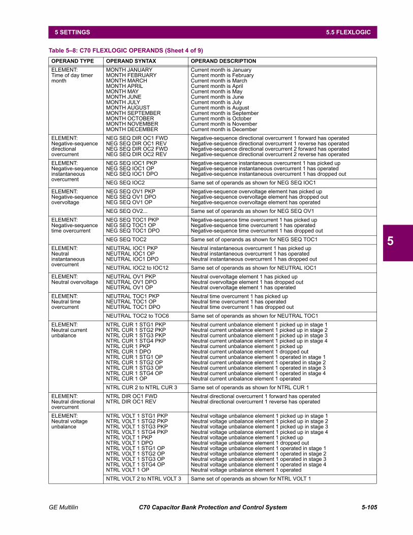
GE Multilin C70 Capacitor Bank Protection and Control System 5-105
5 SETTINGS 5.5 FLEXLOGIC
5
ELEMENT:Time of day timer month
MONTH JANUARYMONTH FEBRUARYMONTH MARCHMONTH APRILMONTH MAYMONTH JUNEMONTH JULYMONTH AUGUSTMONTH SEPTEMBERMONTH OCTOBERMONTH NOVEMBERMONTH DECEMBER
Current month is JanuaryCurrent month is FebruaryCurrent month is MarchCurrent month is AprilCurrent month is MayCurrent month is JuneCurrent month is JulyCurrent month is AugustCurrent month is SeptemberCurrent month is OctoberCurrent month is NovemberCurrent month is December
ELEMENT:Negative-sequence directional overcurrent
NEG SEQ DIR OC1 FWDNEG SEQ DIR OC1 REVNEG SEQ DIR OC2 FWDNEG SEQ DIR OC2 REV
Negative-sequence directional overcurrent 1 forward has operatedNegative-sequence directional overcurrent 1 reverse has operatedNegative-sequence directional overcurrent 2 forward has operatedNegative-sequence directional overcurrent 2 reverse has operated
ELEMENT:Negative-sequence instantaneous overcurrent
NEG SEQ IOC1 PKPNEG SEQ IOC1 OPNEG SEQ IOC1 DPO
Negative-sequence instantaneous overcurrent 1 has picked upNegative-sequence instantaneous overcurrent 1 has operatedNegative-sequence instantaneous overcurrent 1 has dropped out
NEG SEQ IOC2 Same set of operands as shown for NEG SEQ IOC1
ELEMENT:Negative-sequence overvoltage
NEG SEQ OV1 PKPNEG SEQ OV1 DPONEG SEQ OV1 OP
Negative-sequence overvoltage element has picked upNegative-sequence overvoltage element has dropped outNegative-sequence overvoltage element has operated
NEG SEQ OV2... Same set of operands as shown for NEG SEQ OV1
ELEMENT:Negative-sequence time overcurrent
NEG SEQ TOC1 PKPNEG SEQ TOC1 OPNEG SEQ TOC1 DPO
Negative-sequence time overcurrent 1 has picked upNegative-sequence time overcurrent 1 has operatedNegative-sequence time overcurrent 1 has dropped out
NEG SEQ TOC2 Same set of operands as shown for NEG SEQ TOC1
ELEMENT:Neutral instantaneous overcurrent
NEUTRAL IOC1 PKPNEUTRAL IOC1 OPNEUTRAL IOC1 DPO
Neutral instantaneous overcurrent 1 has picked upNeutral instantaneous overcurrent 1 has operatedNeutral instantaneous overcurrent 1 has dropped out
NEUTRAL IOC2 to IOC12 Same set of operands as shown for NEUTRAL IOC1
ELEMENT:Neutral overvoltage
NEUTRAL OV1 PKPNEUTRAL OV1 DPONEUTRAL OV1 OP
Neutral overvoltage element 1 has picked upNeutral overvoltage element 1 has dropped outNeutral overvoltage element 1 has operated
ELEMENT:Neutral time overcurrent
NEUTRAL TOC1 PKPNEUTRAL TOC1 OPNEUTRAL TOC1 DPO
Neutral time overcurrent 1 has picked upNeutral time overcurrent 1 has operatedNeutral time overcurrent 1 has dropped out
NEUTRAL TOC2 to TOC6 Same set of operands as shown for NEUTRAL TOC1
ELEMENT:Neutral current unbalance
NTRL CUR 1 STG1 PKPNTRL CUR 1 STG2 PKPNTRL CUR 1 STG3 PKPNTRL CUR 1 STG4 PKPNTRL CUR 1 PKPNTRL CUR 1 DPONTRL CUR 1 STG1 OPNTRL CUR 1 STG2 OPNTRL CUR 1 STG3 OPNTRL CUR 1 STG4 OPNTRL CUR 1 OP
Neutral current unbalance element 1 picked up in stage 1Neutral current unbalance element 1 picked up in stage 2Neutral current unbalance element 1 picked up in stage 3Neutral current unbalance element 1 picked up in stage 4Neutral current unbalance element 1 picked upNeutral current unbalance element 1 dropped outNeutral current unbalance element 1 operated in stage 1Neutral current unbalance element 1 operated in stage 2Neutral current unbalance element 1 operated in stage 3Neutral current unbalance element 1 operated in stage 4Neutral current unbalance element 1 operated
NTRL CUR 2 to NTRL CUR 3 Same set of operands as shown for NTRL CUR 1
ELEMENT:Neutral directional overcurrent
NTRL DIR OC1 FWDNTRL DIR OC1 REV
Neutral directional overcurrent 1 forward has operatedNeutral directional overcurrent 1 reverse has operated
ELEMENT:Neutral voltage unbalance
NTRL VOLT 1 STG1 PKPNTRL VOLT 1 STG2 PKPNTRL VOLT 1 STG3 PKPNTRL VOLT 1 STG4 PKPNTRL VOLT 1 PKPNTRL VOLT 1 DPONTRL VOLT 1 STG1 OPNTRL VOLT 1 STG2 OPNTRL VOLT 1 STG3 OPNTRL VOLT 1 STG4 OPNTRL VOLT 1 OP
Neutral voltage unbalance element 1 picked up in stage 1Neutral voltage unbalance element 1 picked up in stage 2Neutral voltage unbalance element 1 picked up in stage 3Neutral voltage unbalance element 1 picked up in stage 4Neutral voltage unbalance element 1 picked upNeutral voltage unbalance element 1 dropped outNeutral voltage unbalance element 1 operated in stage 1Neutral voltage unbalance element 1 operated in stage 2Neutral voltage unbalance element 1 operated in stage 3Neutral voltage unbalance element 1 operated in stage 4Neutral voltage unbalance element 1 operated
NTRL VOLT 2 to NTRL VOLT 3 Same set of operands as shown for NTRL VOLT 1
Table 5–8: C70 FLEXLOGIC OPERANDS (Sheet 4 of 9)
OPERAND TYPE OPERAND SYNTAX OPERAND DESCRIPTION
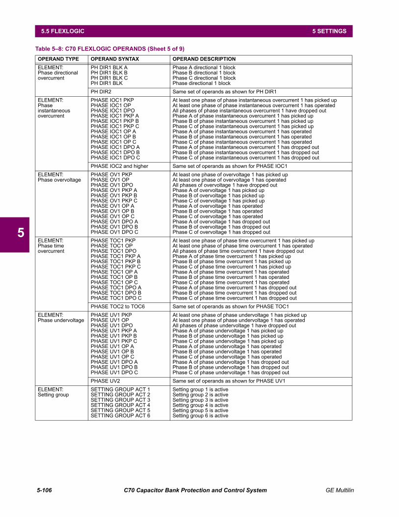
5-106 C70 Capacitor Bank Protection and Control System GE Multilin
5.5 FLEXLOGIC 5 SETTINGS
5
ELEMENT:Phase directional overcurrent
PH DIR1 BLK APH DIR1 BLK BPH DIR1 BLK CPH DIR1 BLK
Phase A directional 1 blockPhase B directional 1 blockPhase C directional 1 blockPhase directional 1 block
PH DIR2 Same set of operands as shown for PH DIR1
ELEMENT:Phase instantaneous overcurrent
PHASE IOC1 PKPPHASE IOC1 OPPHASE IOC1 DPOPHASE IOC1 PKP APHASE IOC1 PKP BPHASE IOC1 PKP CPHASE IOC1 OP APHASE IOC1 OP BPHASE IOC1 OP CPHASE IOC1 DPO APHASE IOC1 DPO BPHASE IOC1 DPO C
At least one phase of phase instantaneous overcurrent 1 has picked upAt least one phase of phase instantaneous overcurrent 1 has operatedAll phases of phase instantaneous overcurrent 1 have dropped outPhase A of phase instantaneous overcurrent 1 has picked upPhase B of phase instantaneous overcurrent 1 has picked upPhase C of phase instantaneous overcurrent 1 has picked upPhase A of phase instantaneous overcurrent 1 has operatedPhase B of phase instantaneous overcurrent 1 has operatedPhase C of phase instantaneous overcurrent 1 has operatedPhase A of phase instantaneous overcurrent 1 has dropped outPhase B of phase instantaneous overcurrent 1 has dropped outPhase C of phase instantaneous overcurrent 1 has dropped out
PHASE IOC2 and higher Same set of operands as shown for PHASE IOC1
ELEMENT:Phase overvoltage
PHASE OV1 PKPPHASE OV1 OPPHASE OV1 DPOPHASE OV1 PKP APHASE OV1 PKP BPHASE OV1 PKP CPHASE OV1 OP APHASE OV1 OP BPHASE OV1 OP CPHASE OV1 DPO APHASE OV1 DPO BPHASE OV1 DPO C
At least one phase of overvoltage 1 has picked upAt least one phase of overvoltage 1 has operatedAll phases of overvoltage 1 have dropped outPhase A of overvoltage 1 has picked upPhase B of overvoltage 1 has picked upPhase C of overvoltage 1 has picked upPhase A of overvoltage 1 has operatedPhase B of overvoltage 1 has operatedPhase C of overvoltage 1 has operatedPhase A of overvoltage 1 has dropped outPhase B of overvoltage 1 has dropped outPhase C of overvoltage 1 has dropped out
ELEMENT:Phase time overcurrent
PHASE TOC1 PKPPHASE TOC1 OPPHASE TOC1 DPOPHASE TOC1 PKP APHASE TOC1 PKP BPHASE TOC1 PKP CPHASE TOC1 OP APHASE TOC1 OP BPHASE TOC1 OP CPHASE TOC1 DPO APHASE TOC1 DPO BPHASE TOC1 DPO C
At least one phase of phase time overcurrent 1 has picked upAt least one phase of phase time overcurrent 1 has operatedAll phases of phase time overcurrent 1 have dropped outPhase A of phase time overcurrent 1 has picked upPhase B of phase time overcurrent 1 has picked upPhase C of phase time overcurrent 1 has picked upPhase A of phase time overcurrent 1 has operatedPhase B of phase time overcurrent 1 has operatedPhase C of phase time overcurrent 1 has operatedPhase A of phase time overcurrent 1 has dropped outPhase B of phase time overcurrent 1 has dropped outPhase C of phase time overcurrent 1 has dropped out
PHASE TOC2 to TOC6 Same set of operands as shown for PHASE TOC1
ELEMENT:Phase undervoltage
PHASE UV1 PKPPHASE UV1 OPPHASE UV1 DPOPHASE UV1 PKP APHASE UV1 PKP BPHASE UV1 PKP CPHASE UV1 OP APHASE UV1 OP BPHASE UV1 OP CPHASE UV1 DPO APHASE UV1 DPO BPHASE UV1 DPO C
At least one phase of phase undervoltage 1 has picked upAt least one phase of phase undervoltage 1 has operatedAll phases of phase undervoltage 1 have dropped outPhase A of phase undervoltage 1 has picked upPhase B of phase undervoltage 1 has picked upPhase C of phase undervoltage 1 has picked upPhase A of phase undervoltage 1 has operatedPhase B of phase undervoltage 1 has operatedPhase C of phase undervoltage 1 has operatedPhase A of phase undervoltage 1 has dropped outPhase B of phase undervoltage 1 has dropped outPhase C of phase undervoltage 1 has dropped out
PHASE UV2 Same set of operands as shown for PHASE UV1
ELEMENT:Setting group
SETTING GROUP ACT 1SETTING GROUP ACT 2SETTING GROUP ACT 3SETTING GROUP ACT 4SETTING GROUP ACT 5SETTING GROUP ACT 6
Setting group 1 is activeSetting group 2 is activeSetting group 3 is activeSetting group 4 is activeSetting group 5 is activeSetting group 6 is active
Table 5–8: C70 FLEXLOGIC OPERANDS (Sheet 5 of 9)
OPERAND TYPE OPERAND SYNTAX OPERAND DESCRIPTION

GE Multilin C70 Capacitor Bank Protection and Control System 5-107
5 SETTINGS 5.5 FLEXLOGIC
5
ELEMENT:Sub-harmonic stator ground fault detector
SH STAT GND STG1 PKPSH STAT GND STG1 DPOSH STAT GND STG1 OPSH STAT GND STG2 PKPSH STAT GND STG2 DPOSH STAT GND STG2 OPSH STAT GND OC PKP
SH STAT GND OC DPO
SH STAT GND OC OP
SH STAT GND TRB PKPSH STAT GND TRB DPOSH STAT GND TRB OP
Stage 1 of the sub-harmonic stator ground protection has picked upStage 1 of the sub-harmonic stator ground protection has dropped outStage 1 of the sub-harmonic stator ground protection has operatedStage 2 of the sub-harmonic stator ground protection has picked upStage 2 of the sub-harmonic stator ground protection has dropped outStage 2 of the sub-harmonic stator ground protection has operatedGround over current element of the sub-harmonic stator ground protection has picked upGround over current element of the sub-harmonic stator ground protection has dropped outGround over current element of the sub-harmonic stator ground protection has operatedSub-harmonic stator ground module trouble has picked upSub-harmonic stator ground module trouble has dropped outSub-harmonic stator ground module trouble has operated
ELEMENT:Disturbance detector
SRC1 50DD OPSRC2 50DD OPSRC3 50DD OPSRC4 50DD OPSRC5 50DD OPSRC6 50DD OP
Source 1 disturbance detector has operatedSource 2 disturbance detector has operatedSource 3 disturbance detector has operatedSource 4 disturbance detector has operatedSource 5 disturbance detector has operatedSource 6 disturbance detector has operated
ELEMENT:VTFF (Voltage transformer fuse failure)
SRC1 VT FUSE FAIL OPSRC1 VT FUSE FAIL DPOSRC1 VT FUSE FAIL VOL LOSS
Source 1 VT fuse failure detector has operatedSource 1 VT fuse failure detector has dropped outSource 1 has lost voltage signals (V2 below 15% AND V1 below 5%
of nominal)
SRC1 VT NEU WIRE OPEN Source 1 VT neutral wire open detected.
SRC2 VT FUSE FAIL toSRC6 VT FUSE FAIL
Same set of operands as shown for SRC1 VT FUSE FAIL
ELEMENT:Disconnect switch
SWITCH 1 OFF CMDSWITCH 1 ON CMDSWITCH 1 A BAD ST
SWITCH 1 A INTERM
SWITCH 1 A CLSDSWITCH 1 A OPENSWITCH 1 B BAD ST
SWITCH 1 C INTERM
SWITCH 1 B CLSDSWITCH 1 B OPENSWITCH 1 C BAD ST
SWITCH 1 A INTERM
SWITCH 1 C CLSDSWITCH 1 C OPENSWITCH 1 BAD STATUSSWITCH 1 CLOSEDSWITCH 1 OPENSWITCH 1 DISCREPSWITCH 1 TROUBLE
Disconnect switch 1 open command initiatedDisconnect switch 1 close command initiatedDisconnect switch 1 phase A bad status is detected (discrepancy between
the 89/a and 89/b contacts)Disconnect switch 1 phase A intermediate status is detected (transition from
one position to another)Disconnect switch 1 phase A is closedDisconnect switch 1 phase A is openDisconnect switch 1 phase B bad status is detected (discrepancy between
the 89/a and 89/b contacts)Disconnect switch 1 phase C intermediate status is detected (transition from
one position to another)Disconnect switch 1 phase B is closedDisconnect switch 1 phase B is openDisconnect switch 1 phase C bad status is detected (discrepancy between
the 89/a and 89/b contacts)Disconnect switch 1 phase A intermediate status is detected (transition from
one position to another)Disconnect switch 1 phase C is closedDisconnect switch 1 phase C is openDisconnect switch 1 bad status is detected on any poleDisconnect switch 1 is closedDisconnect switch 1 is openDisconnect switch 1 has discrepancyDisconnect switch 1 trouble alarm
SWITCH 2... Same set of operands as shown for SWITCH 1
ELEMENT:Time of day timer
TIME OF DAY 1 ONTIME OF DAY 1 STARTTIME OF DAY 1 STOP
Time of day timer 1 is onOne-second pulse at set time of day timer 1 start timeOne-second pulse at set time of day timer 1 stop time
TIME OF DAY 2 to 5 Same set of operands as shown for TIME OF DAY 1
ELEMENTTrip bus
TRIP BUS 1 PKPTRIP BUS 1 OP
Asserted when the trip bus 1 element picks up.Asserted when the trip bus 1 element operates.
TRIP BUS 2... Same set of operands as shown for TRIP BUS 1
Table 5–8: C70 FLEXLOGIC OPERANDS (Sheet 6 of 9)
OPERAND TYPE OPERAND SYNTAX OPERAND DESCRIPTION

5-108 C70 Capacitor Bank Protection and Control System GE Multilin
5.5 FLEXLOGIC 5 SETTINGS
5
ELEMENT:Voltage differential
VOLT DIF 1 STG1A PKPVOLT DIF 1 STG1B PKPVOLT DIF 1 STG1C PKPVOLT DIF 1 STG2A PKPVOLT DIF 1 STG2B PKPVOLT DIF 1 STG2C PKPVOLT DIF 1 STG3A PKPVOLT DIF 1 STG3B PKPVOLT DIF 1 STG3C PKPVOLT DIF 1 STG4A PKPVOLT DIF 1 STG4B PKPVOLT DIF 1 STG4C PKPVOLT DIF 1 PKP AVOLT DIF 1 PKP BVOLT DIF 1 PKP CVOLT DIF 1 PKPVOLT DIF 1 DPOVOLT DIF 1 STG1A OPVOLT DIF 1 STG1B OPVOLT DIF 1 STG1C OPVOLT DIF 1 STG2A OPVOLT DIF 1 STG2B OPVOLT DIF 1 STG2C OPVOLT DIF 1 STG3A OPVOLT DIF 1 STG3B OPVOLT DIF 1 STG3C OPVOLT DIF 1 STG4A OPVOLT DIF 1 STG4B OPVOLT DIF 1 STG4C OPVOLT DIF 1 OP AVOLT DIF 1 OP BVOLT DIF 1 OP CVOLT DIF 1 OP
Voltage differential element 1 picked up in phase A of stage 1Voltage differential element 1 picked up in phase B of stage 1Voltage differential element 1 picked up in phase C of stage 1Voltage differential element 1 picked up in phase A of stage 2Voltage differential element 1 picked up in phase B of stage 2Voltage differential element 1 picked up in phase C of stage 2Voltage differential element 1 picked up in phase A of stage 3Voltage differential element 1 picked up in phase B of stage 3Voltage differential element 1 picked up in phase C of stage 3Voltage differential element 1 picked up in phase A of stage 4Voltage differential element 1 picked up in phase B of stage 4Voltage differential element 1 picked up in phase C of stage 4Voltage differential element 1 picked up in phase AVoltage differential element 1 picked up in phase BVoltage differential element 1 picked up in phase CVoltage differential element 1 picked upVoltage differential element 1 dropped outVoltage differential element 1 operated in phase A of stage 1Voltage differential element 1 operated in phase B of stage 1Voltage differential element 1 operated in phase C of stage 1Voltage differential element 1 operated in phase A of stage 2Voltage differential element 1 operated in phase B of stage 2Voltage differential element 1 operated in phase C of stage 2Voltage differential element 1 operated in phase A of stage 3Voltage differential element 1 operated in phase B of stage 3Voltage differential element 1 operated in phase C of stage 3Voltage differential element 1 operated in phase A of stage 4Voltage differential element 1 operated in phase B of stage 4Voltage differential element 1 operated in phase C of stage 4Voltage differential element 1 operated in phase AVoltage differential element 1 operated in phase BVoltage differential element 1 operated in phase CVoltage differential element 1 operated
VOLT DIF 2 to 3 Same set of operands as shown for VOLT DIF 1 above
FIXED OPERANDS Off Logic = 0. Does nothing and may be used as a delimiter in an equation list; used as ‘Disable’ by other features.
On Logic = 1. Can be used as a test setting.
INPUTS/OUTPUTS:Contact inputs
Cont Ip 1 OnCont Ip 2 On
Cont Ip 1 OffCont Ip 2 Off
(will not appear unless ordered)(will not appear unless ordered)
(will not appear unless ordered)(will not appear unless ordered)
INPUTS/OUTPUTS:Contact outputs, current(from detector on form-A output only)
Cont Op 1 IOnCont Op 2 IOn
(will not appear unless ordered)(will not appear unless ordered)
INPUTS/OUTPUTS:Contact outputs, voltage(from detector on form-A output only)
Cont Op 1 VOnCont Op 2 VOn
(will not appear unless ordered)(will not appear unless ordered)
Cont Op 1 VOffCont Op 2 VOff
(will not appear unless ordered)(will not appear unless ordered)
INPUTS/OUTPUTSDirect inputs
DIRECT INPUT 1 On
DIRECT INPUT 32 On
Flag is set, logic=1
Flag is set, logic=1
INPUTS/OUTPUTS:Remote double-point status inputs
RemDPS Ip 1 BADRemDPS Ip 1 INTERM
RemDPS Ip 1 OFFRemDPS Ip 1 ON
Asserted while the remote double-point status input is in the bad state.Asserted while the remote double-point status input is in the intermediate
state.Asserted while the remote double-point status input is off.Asserted while the remote double-point status input is on.
REMDPS Ip 2... Same set of operands as per REMDPS 1 above
INPUTS/OUTPUTS:Remote inputs
REMOTE INPUT 1 OnREMOTE INPUT 2 OnREMOTE INPUT 2 On
REMOTE INPUT 32 On
Flag is set, logic=1Flag is set, logic=1Flag is set, logic=1
Flag is set, logic=1
Table 5–8: C70 FLEXLOGIC OPERANDS (Sheet 7 of 9)
OPERAND TYPE OPERAND SYNTAX OPERAND DESCRIPTION

GE Multilin C70 Capacitor Bank Protection and Control System 5-109
5 SETTINGS 5.5 FLEXLOGIC
5
INPUTS/OUTPUTS:Virtual inputs
Virt Ip 1 OnVirt Ip 2 OnVirt Ip 3 On
Virt Ip 64 On
Flag is set, logic=1Flag is set, logic=1Flag is set, logic=1
Flag is set, logic=1
INPUTS/OUTPUTS:Virtual outputs
Virt Op 1 OnVirt Op 2 OnVirt Op 3 On
Virt Op 96 On
Flag is set, logic=1Flag is set, logic=1Flag is set, logic=1
Flag is set, logic=1
LED INDICATORS:Fixed front panel LEDs
LED IN SERVICELED TROUBLELED TEST MODELED TRIPLED ALARMLED PICKUPLED VOLTAGELED CURRENTLED FREQUENCYLED OTHERLED PHASE ALED PHASE BLED PHASE CLED NEUTRAL/GROUND
Asserted when the front panel IN SERVICE LED is on.Asserted when the front panel TROUBLE LED is on.Asserted when the front panel TEST MODE LED is on.Asserted when the front panel TRIP LED is on.Asserted when the front panel ALARM LED is on.Asserted when the front panel PICKUP LED is on.Asserted when the front panel VOLTAGE LED is on.Asserted when the front panel CURRENT LED is on.Asserted when the front panel FREQUENCY LED is on.Asserted when the front panel OTHER LED is on.Asserted when the front panel PHASE A LED is on.Asserted when the front panel PHASE B LED is on.Asserted when the front panel PHASE C LED is on.Asserted when the front panel NEUTRAL/GROUND LED is on.
LED INDICATORS:LED test
LED TEST IN PROGRESS An LED test has been initiated and has not finished.
LED INDICATORS:User-programmable LEDs
LED USER 1 Asserted when user-programmable LED 1 is on.
LED USER 2 to 48 The operand above is available for user-programmable LEDs 2 through 48.
PASSWORD SECURITY
ACCESS LOC SETG OFFACCESS LOC SETG ONACCESS LOC CMND OFFACCESS LOC CMND ONACCESS REM SETG OFFACCESS REM SETG ONACCESS REM CMND OFFACCESS REM CMND ONUNAUTHORIZED ACCESS
Asserted when local setting access is disabled.Asserted when local setting access is enabled.Asserted when local command access is disabled.Asserted when local command access is enabled.Asserted when remote setting access is disabled.Asserted when remote setting access is enabled.Asserted when remote command access is disabled.Asserted when remote command access is enabled.Asserted when a password entry fails while accessing a password protected
level of the C70.
REMOTE DEVICES REMOTE DEVICE 1 OnREMOTE DEVICE 2 OnREMOTE DEVICE 2 On
REMOTE DEVICE 16 On
Flag is set, logic=1Flag is set, logic=1Flag is set, logic=1
Flag is set, logic=1
REMOTE DEVICE 1 OffREMOTE DEVICE 2 OffREMOTE DEVICE 3 Off
REMOTE DEVICE 16 Off
Flag is set, logic=1Flag is set, logic=1Flag is set, logic=1
Flag is set, logic=1
RESETTING RESET OPRESET OP (COMMS)RESET OP (OPERAND)
RESET OP (PUSHBUTTON)
Reset command is operated (set by all three operands below).Communications source of the reset command.Operand (assigned in the INPUTS/OUTPUTS RESETTING menu) source
of the reset command.Reset key (pushbutton) source of the reset command.
Table 5–8: C70 FLEXLOGIC OPERANDS (Sheet 8 of 9)
OPERAND TYPE OPERAND SYNTAX OPERAND DESCRIPTION

5-110 C70 Capacitor Bank Protection and Control System GE Multilin
5.5 FLEXLOGIC 5 SETTINGS
5 Some operands can be re-named by the user. These are the names of the breakers in the breaker control feature, the ID(identification) of contact inputs, the ID of virtual inputs, and the ID of virtual outputs. If the user changes the default nameor ID of any of these operands, the assigned name will appear in the relay list of operands. The default names are shown inthe FlexLogic operands table above.
The characteristics of the logic gates are tabulated below, and the operators available in FlexLogic are listed in the Flex-Logic operators table.
SELF-DIAGNOSTICS(See Relay Self-tests descriptions in Chapter 7: Commands and Targets)
ANY MAJOR ERRORANY MINOR ERRORANY SELF-TESTSBATTERY FAILCLOCK UNSYNCHRONIZEDDIRECT DEVICE OFFDIRECT RING BREAKEQUIPMENT MISMATCHFLEXLOGIC ERR TOKENLATCHING OUT ERRORMAINTENANCE ALERTFIRST ETHERNET FAILPROCESS BUS FAILUREPTP FAILUREREMOTE DEVICE OFFRRTD COMM FAILSECOND ETHERNET FAILTHIRD ETHERNET FAILSNTP FAILURESYSTEM EXCEPTIONTEMP MONITORUNIT NOT PROGRAMMED
Any of the major self-test errors generated (major error)Any of the minor self-test errors generated (minor error)Any self-test errors generated (generic, any error)The battery is not functioning. Return power supply module to manufacturer.Relay is not synchronized to the international time standardA direct device is configured but not connectedThe Direct I/O settings is for a connection that is not in a ringThe configuration of modules does not match the stored order codeA FlexLogic equation is incorrectA difference is detected between the desired and actual latch contact stateA subset of the minor self-test errors generated, see Chapter 7See description in Chapter 7: Commands and targetsSee description in Chapter 7: Commands and targets"Bad PTP Signal" self-test as described in Chapter 7One or more GOOSE devices are not respondingSee description in Chapter 7: Commands and targetsSee description in Chapter 7: Commands and targetsSee description in Chapter 7: Commands and targetsSNTP server is not respondingSee description in Chapter 7: Commands and targetsMonitors ambient temperature and maximum operating temperatureThe product setup>installation>relay settings setting is not programmed
TEMPERATURE MONITOR
TEMP MONITOR Asserted while the ambient temperature is greater than the maximum operating temperature (80°C)
USER-PROGRAMMABLE PUSHBUTTONS
PUSHBUTTON 1 ONPUSHBUTTON 1 OFFANY PB ON
Pushbutton number 1 is in the “On” positionPushbutton number 1 is in the “Off” positionAny of twelve pushbuttons is in the “On” position
PUSHBUTTON 2 to 12 Same set of operands as PUSHBUTTON 1
Table 5–9: FLEXLOGIC GATE CHARACTERISTICS
GATES NUMBER OF INPUTS OUTPUT IS ‘1’ (= ON) IF...
NOT 1 input is ‘0’
OR 2 to 16 any input is ‘1’
AND 2 to 16 all inputs are ‘1’
NOR 2 to 16 all inputs are ‘0’
NAND 2 to 16 any input is ‘0’
XOR 2 only one input is ‘1’
Table 5–8: C70 FLEXLOGIC OPERANDS (Sheet 9 of 9)
OPERAND TYPE OPERAND SYNTAX OPERAND DESCRIPTION

GE Multilin C70 Capacitor Bank Protection and Control System 5-111
5 SETTINGS 5.5 FLEXLOGIC
5
5.5.2 FLEXLOGIC RULES
When forming a FlexLogic equation, the sequence in the linear array of parameters must follow these general rules:
1. Operands must precede the operator which uses the operands as inputs.
2. Operators have only one output. The output of an operator must be used to create a virtual output if it is to be used asan input to two or more operators.
3. Assigning the output of an operator to a virtual output terminates the equation.
4. A timer operator (for example, "TIMER 1") or virtual output assignment (for example, " = Virt Op 1") may only be usedonce. If this rule is broken, a syntax error will be declared.
5.5.3 FLEXLOGIC EVALUATION
Each equation is evaluated in the order in which the parameters have been entered.
FlexLogic provides latches which by definition have a memory action, remaining in the set state after the set inputhas been asserted. However, they are volatile; that is, they reset on the re-application of control power.
When making changes to settings, all FlexLogic equations are re-compiled whenever any new setting value isentered, so all latches are automatically reset. If it is necessary to re-initialize FlexLogic during testing, for example,it is suggested to power the unit down and then back up.
Table 5–10: FLEXLOGIC OPERATORS
TYPE SYNTAX DESCRIPTION NOTES
Editor INSERT Insert a parameter in an equation list.
DELETE Delete a parameter from an equation list.
End END The first END encountered signifies the last entry in the list of processed FlexLogic parameters.
One-shot POSITIVE ONE SHOT One shot that responds to a positive going edge. A ‘one shot’ refers to a single input gate that generates a pulse in response to an edge on the input. The output from a ‘one shot’ is True (positive) for only one pass through the FlexLogic equation. There is a maximum of 64 ‘one shots’.
NEGATIVE ONE SHOT
One shot that responds to a negative going edge.
DUAL ONE SHOT One shot that responds to both the positive and negative going edges.
Logicgate
NOT Logical NOT Operates on the previous parameter.
OR(2)
OR(16)
2 input OR gate
16 input OR gate
Operates on the 2 previous parameters.
Operates on the 16 previous parameters.
AND(2)
AND(16)
2 input AND gate
16 input AND gate
Operates on the 2 previous parameters.
Operates on the 16 previous parameters.
NOR(2)
NOR(16)
2 input NOR gate
16 input NOR gate
Operates on the 2 previous parameters.
Operates on the 16 previous parameters.
NAND(2)
NAND(16)
2 input NAND gate
16 input NAND gate
Operates on the 2 previous parameters.
Operates on the 16 previous parameters.
XOR(2) 2 input Exclusive OR gate Operates on the 2 previous parameters.
LATCH (S,R) Latch (set, reset): reset-dominant The parameter preceding LATCH(S,R) is the reset input. The parameter preceding the reset input is the set input.
Timer TIMER 1
TIMER 32
Timer set with FlexLogic timer 1 settings.
Timer set with FlexLogic timer 32 settings.
The timer is started by the preceding parameter. The output of the timer is TIMER #.
Assign virtualoutput
= Virt Op 1
= Virt Op 96
Assigns previous FlexLogic operand to virtual output 1.
Assigns previous FlexLogic operand to virtual output 96.
The virtual output is set by the preceding parameter
NOTE

5-112 C70 Capacitor Bank Protection and Control System GE Multilin
5.5 FLEXLOGIC 5 SETTINGS
5
5.5.4 FLEXLOGIC EXAMPLE
This section provides an example of implementing logic for a typical application. The sequence of the steps is quite impor-tant as it should minimize the work necessary to develop the relay settings. Note that the example presented in the figurebelow is intended to demonstrate the procedure, not to solve a specific application situation.
In the example below, it is assumed that logic has already been programmed to produce virtual outputs 1 and 2, and is onlya part of the full set of equations used. When using FlexLogic, it is important to make a note of each virtual output used – avirtual output designation (1 to 96) can only be properly assigned once.
Figure 5–38: EXAMPLE LOGIC SCHEME
1. Inspect the example logic diagram to determine if the required logic can be implemented with the FlexLogic operators.If this is not possible, the logic must be altered until this condition is satisfied. Once this is done, count the inputs toeach gate to verify that the number of inputs does not exceed the FlexLogic limits, which is unlikely but possible. If thenumber of inputs is too high, subdivide the inputs into multiple gates to produce an equivalent. For example, if 25inputs to an AND gate are required, connect Inputs 1 through 16 to AND(16), 17 through 25 to AND(9), and the outputsfrom these two gates to AND(2).
Inspect each operator between the initial operands and final virtual outputs to determine if the output from the operatoris used as an input to more than one following operator. If so, the operator output must be assigned as a virtual output.
For the example shown above, the output of the AND gate is used as an input to both OR#1 and Timer 1, and musttherefore be made a virtual output and assigned the next available number (i.e. Virtual Output 3). The final output mustalso be assigned to a virtual output as virtual output 4, which will be programmed in the contact output section to oper-ate relay H1 (that is, contact output H1).
Therefore, the required logic can be implemented with two FlexLogic equations with outputs of virtual output 3 and vir-tual output 4 as shown below.
Figure 5–39: LOGIC EXAMPLE WITH VIRTUAL OUTPUTS
LATCH
CONTACT INPUT H1cState=Closed
XOR
AND
Reset
SetVIRTUAL OUTPUT 2State=ON
VIRTUAL INPUT 1State=ON
DIGITAL ELEMENT 1State=Pickup
DIGITAL ELEMENT 2State=Operated
OR #2 Operate OutputRelay H1
OR #1
(800 ms)
Timer 1Time Delayon Pickup
(200 ms)
Timer 2Time Delayon Dropout
VIRTUAL OUTPUT 1State=ON
827025A2.vsd
LATCH
CONTACT INPUT H1cState=Closed
XOR
AND
Reset
SetVIRTUAL OUTPUT 2State=ON
VIRTUAL INPUT 1State=ON
DIGITAL ELEMENT 1State=Pickup
DIGITAL ELEMENT 2State=Operated
OR #2 VIRTUAL OUTPUT 4
OR #1
(800 ms)
Timer 1Time Delayon Pickup
(200 ms)
Timer 2Time Delayon Dropout
VIRTUAL OUTPUT 1State=ON
827026A2.VSD
VIRTUAL OUTPUT 3

GE Multilin C70 Capacitor Bank Protection and Control System 5-113
5 SETTINGS 5.5 FLEXLOGIC
5
2. Prepare a logic diagram for the equation to produce virtual output 3, as this output will be used as an operand in thevirtual output 4 equation (create the equation for every output that will be used as an operand first, so that when theseoperands are required they will already have been evaluated and assigned to a specific virtual output). The logic forvirtual output 3 is shown below with the final output assigned.
Figure 5–40: LOGIC FOR VIRTUAL OUTPUT 3
3. Prepare a logic diagram for virtual output 4, replacing the logic ahead of virtual output 3 with a symbol identified as vir-tual output 3, as shown below.
Figure 5–41: LOGIC FOR VIRTUAL OUTPUT 4
4. Program the FlexLogic equation for virtual output 3 by translating the logic into available FlexLogic parameters. Theequation is formed one parameter at a time until the required logic is complete. It is generally easier to start at the out-put end of the equation and work back towards the input, as shown in the following steps. It is also recommended to listoperator inputs from bottom to top. For demonstration, the final output will be arbitrarily identified as parameter 99, andeach preceding parameter decremented by one in turn. Until accustomed to using FlexLogic, it is suggested that aworksheet with a series of cells marked with the arbitrary parameter numbers be prepared, as shown below.
Figure 5–42: FLEXLOGIC WORKSHEET
5. Following the procedure outlined, start with parameter 99, as follows:
99: The final output of the equation is virtual output 3, which is created by the operator "= Virt Op n". This parameter istherefore "= Virt Op 3."
CONTACT INPUT H1cState=Closed
AND(2)
DIGITAL ELEMENT 2State=Operated
VIRTUAL OUTPUT 3
827027A2.VSD
LATCH
CONTACT INPUT H1cState=Closed
XOR
Reset
SetVIRTUAL OUTPUT 2State=ON
VIRTUAL INPUT 1State=ON
DIGITAL ELEMENT 1State=Pickup
OR #2 VIRTUALOUTPUT 4
OR #1
(800 ms)
Timer 1Time Delayon Pickup
(200 ms)
Timer 2Time Delayon Dropout
VIRTUAL OUTPUT 3State=ON
VIRTUAL OUTPUT 1State=ON
827028A2.VSD
01
02
03
04
05
97
98
99
.....
827029A1.VSD

5-114 C70 Capacitor Bank Protection and Control System GE Multilin
5.5 FLEXLOGIC 5 SETTINGS
5
98: The gate preceding the output is an AND, which in this case requires two inputs. The operator for this gate is a 2-input AND so the parameter is “AND(2)”. Note that FlexLogic rules require that the number of inputs to most typesof operators must be specified to identify the operands for the gate. As the 2-input AND will operate on the twooperands preceding it, these inputs must be specified, starting with the lower.
97: This lower input to the AND gate must be passed through an inverter (the NOT operator) so the next parameter is“NOT”. The NOT operator acts upon the operand immediately preceding it, so specify the inverter input next.
96: The input to the NOT gate is to be contact input H1c. The ON state of a contact input can be programmed to beset when the contact is either open or closed. Assume for this example the state is to be ON for a closed contact.The operand is therefore “Cont Ip H1c On”.
95: The last step in the procedure is to specify the upper input to the AND gate, the operated state of digital element 2.This operand is "DIG ELEM 2 OP".
Writing the parameters in numerical order can now form the equation for virtual output 3:
[95] DIG ELEM 2 OP[96] Cont Ip H1c On[97] NOT[98] AND(2)[99] = Virt Op 3
It is now possible to check that this selection of parameters will produce the required logic by converting the set of parame-ters into a logic diagram. The result of this process is shown below, which is compared to the logic for virtual output 3 dia-gram as a check.
Figure 5–43: FLEXLOGIC EQUATION FOR VIRTUAL OUTPUT 3
6. Repeating the process described for virtual output 3, select the FlexLogic parameters for Virtual Output 4.
99: The final output of the equation is virtual output 4 which is parameter “= Virt Op 4".
98: The operator preceding the output is timer 2, which is operand “TIMER 2". Note that the settings required for thetimer are established in the timer programming section.
97: The operator preceding timer 2 is OR #2, a 3-input OR, which is parameter “OR(3)”.
96: The lowest input to OR #2 is operand “Cont Ip H1c On”.
95: The center input to OR #2 is operand “TIMER 1".
94: The input to timer 1 is operand “Virt Op 3 On".
93: The upper input to OR #2 is operand “LATCH (S,R)”.
92: There are two inputs to a latch, and the input immediately preceding the latch reset is OR #1, a 4-input OR, whichis parameter “OR(4)”.
91: The lowest input to OR #1 is operand “Virt Op 3 On".
90: The input just above the lowest input to OR #1 is operand “XOR(2)”.
89: The lower input to the XOR is operand “DIG ELEM 1 PKP”.
88: The upper input to the XOR is operand “Virt Ip 1 On".
87: The input just below the upper input to OR #1 is operand “Virt Op 2 On".
86: The upper input to OR #1 is operand “Virt Op 1 On".
85: The last parameter is used to set the latch, and is operand “Virt Op 4 On".
FLEXLOGIC ENTRY n:NOTFLEXLOGIC ENTRY n:AND (2)FLEXLOGIC ENTRY n:=Virt Op 3
97
98
99
FLEXLOGIC ENTRY n:DIG ELEM 2 OPFLEXLOGIC ENTRY n:Cont Ip H1c On
95
96AND VIRTUAL
OUTPUT 3
827030A2.VSD

GE Multilin C70 Capacitor Bank Protection and Control System 5-115
5 SETTINGS 5.5 FLEXLOGIC
5
The equation for virtual output 4 is:
[85] Virt Op 4 On[86] Virt Op 1 On[87] Virt Op 2 On[88] Virt Ip 1 On[89] DIG ELEM 1 PKP[90] XOR(2)[91] Virt Op 3 On[92] OR(4)[93] LATCH (S,R)[94] Virt Op 3 On[95] TIMER 1[96] Cont Ip H1c On[97] OR(3)[98] TIMER 2[99] = Virt Op 4
It is now possible to check that the selection of parameters will produce the required logic by converting the set of parame-ters into a logic diagram. The result of this process is shown below, which is compared to the logic for virtual output 4 dia-gram as a check.
Figure 5–44: FLEXLOGIC EQUATION FOR VIRTUAL OUTPUT 4
7. Now write the complete FlexLogic expression required to implement the logic, making an effort to assemble the equa-tion in an order where Virtual Outputs that will be used as inputs to operators are created before needed. In caseswhere a lot of processing is required to perform logic, this may be difficult to achieve, but in most cases will not causeproblems as all logic is calculated at least four times per power frequency cycle. The possibility of a problem caused bysequential processing emphasizes the necessity to test the performance of FlexLogic before it is placed in service.
In the following equation, virtual output 3 is used as an input to both latch 1 and timer 1 as arranged in the order shownbelow:
DIG ELEM 2 OPCont Ip H1c OnNOTAND(2)
FLEXLOGIC ENTRY n:Virt Op 3 OnFLEXLOGIC ENTRY n:OR (4)FLEXLOGIC ENTRY n:LATCH (S,R)
91
92
93
FLEXLOGIC ENTRY n:DIG ELEM 1 PKPFLEXLOGIC ENTRY n:XOR
89
90
XOR
FLEXLOGIC ENTRY n:Virt Op 1 OnFLEXLOGIC ENTRY n:Virt Op 2 OnFLEXLOGIC ENTRY n:Virt Ip 1 On
86
87
88
FLEXLOGIC ENTRY n:Virt Op 4 On85
FLEXLOGIC ENTRY n:=Virt Op 499
FLEXLOGIC ENTRY n:OR (3)FLEXLOGIC ENTRY n:TIMER 2
96
97
98
FLEXLOGIC ENTRY n:Virt Op 3 OnFLEXLOGIC ENTRY n:TIMER 1
94
95
LATCHReset
Set
OR
OR
T1
T2 VIRTUALOUTPUT 4
827031A2.VSD
FLEXLOGIC ENTRY n:Cont Ip H1c On
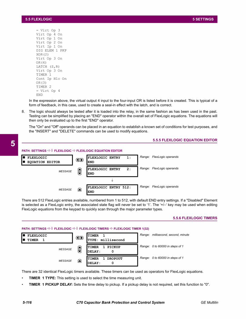
5-116 C70 Capacitor Bank Protection and Control System GE Multilin
5.5 FLEXLOGIC 5 SETTINGS
5
= Virt Op 3Virt Op 4 OnVirt Op 1 OnVirt Op 2 OnVirt Ip 1 OnDIG ELEM 1 PKPXOR(2)Virt Op 3 OnOR(4)LATCH (S,R)Virt Op 3 OnTIMER 1Cont Ip H1c OnOR(3)TIMER 2= Virt Op 4END
In the expression above, the virtual output 4 input to the four-input OR is listed before it is created. This is typical of aform of feedback, in this case, used to create a seal-in effect with the latch, and is correct.
8. The logic should always be tested after it is loaded into the relay, in the same fashion as has been used in the past.Testing can be simplified by placing an "END" operator within the overall set of FlexLogic equations. The equations willthen only be evaluated up to the first "END" operator.
The "On" and "Off" operands can be placed in an equation to establish a known set of conditions for test purposes, andthe "INSERT" and "DELETE" commands can be used to modify equations.
5.5.5 FLEXLOGIC EQUATION EDITOR
PATH: SETTINGS FLEXLOGIC FLEXLOGIC EQUATION EDITOR
There are 512 FlexLogic entries available, numbered from 1 to 512, with default END entry settings. If a "Disabled" Elementis selected as a FlexLogic entry, the associated state flag will never be set to ‘1’. The ‘+/–‘ key may be used when editingFlexLogic equations from the keypad to quickly scan through the major parameter types.
5.5.6 FLEXLOGIC TIMERS
PATH: SETTINGS FLEXLOGIC FLEXLOGIC TIMERS FLEXLOGIC TIMER 1(32)
There are 32 identical FlexLogic timers available. These timers can be used as operators for FlexLogic equations.
• TIMER 1 TYPE: This setting is used to select the time measuring unit.
• TIMER 1 PICKUP DELAY: Sets the time delay to pickup. If a pickup delay is not required, set this function to "0".
FLEXLOGIC EQUATION EDITOR
FLEXLOGIC ENTRY 1:END
Range: FlexLogic operands
MESSAGEFLEXLOGIC ENTRY 2:END
Range: FlexLogic operands
MESSAGEFLEXLOGIC ENTRY 512:END
Range: FlexLogic operands
FLEXLOGIC TIMER 1
TIMER 1TYPE: millisecond
Range: millisecond, second, minute
MESSAGETIMER 1 PICKUPDELAY: 0
Range: 0 to 60000 in steps of 1
MESSAGETIMER 1 DROPOUTDELAY: 0
Range: 0 to 60000 in steps of 1
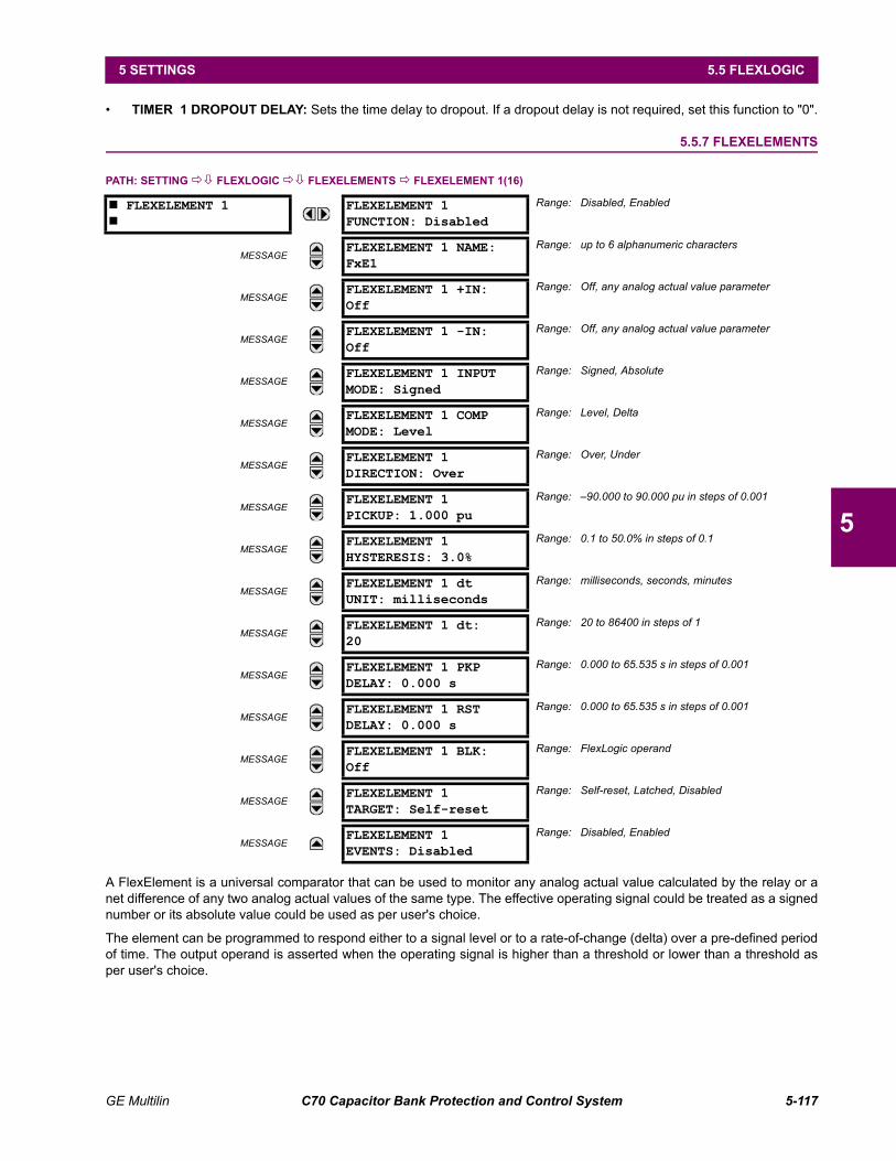
GE Multilin C70 Capacitor Bank Protection and Control System 5-117
5 SETTINGS 5.5 FLEXLOGIC
5
• TIMER 1 DROPOUT DELAY: Sets the time delay to dropout. If a dropout delay is not required, set this function to "0".
5.5.7 FLEXELEMENTS
PATH: SETTING FLEXLOGIC FLEXELEMENTS FLEXELEMENT 1(16)
A FlexElement is a universal comparator that can be used to monitor any analog actual value calculated by the relay or anet difference of any two analog actual values of the same type. The effective operating signal could be treated as a signednumber or its absolute value could be used as per user's choice.
The element can be programmed to respond either to a signal level or to a rate-of-change (delta) over a pre-defined periodof time. The output operand is asserted when the operating signal is higher than a threshold or lower than a threshold asper user's choice.
FLEXELEMENT 1
FLEXELEMENT 1FUNCTION: Disabled
Range: Disabled, Enabled
MESSAGEFLEXELEMENT 1 NAME:FxE1
Range: up to 6 alphanumeric characters
MESSAGEFLEXELEMENT 1 +IN:Off
Range: Off, any analog actual value parameter
MESSAGEFLEXELEMENT 1 -IN:Off
Range: Off, any analog actual value parameter
MESSAGEFLEXELEMENT 1 INPUTMODE: Signed
Range: Signed, Absolute
MESSAGEFLEXELEMENT 1 COMPMODE: Level
Range: Level, Delta
MESSAGEFLEXELEMENT 1DIRECTION: Over
Range: Over, Under
MESSAGEFLEXELEMENT 1PICKUP: 1.000 pu
Range: –90.000 to 90.000 pu in steps of 0.001
MESSAGEFLEXELEMENT 1HYSTERESIS: 3.0%
Range: 0.1 to 50.0% in steps of 0.1
MESSAGEFLEXELEMENT 1 dtUNIT: milliseconds
Range: milliseconds, seconds, minutes
MESSAGEFLEXELEMENT 1 dt:20
Range: 20 to 86400 in steps of 1
MESSAGEFLEXELEMENT 1 PKPDELAY: 0.000 s
Range: 0.000 to 65.535 s in steps of 0.001
MESSAGEFLEXELEMENT 1 RSTDELAY: 0.000 s
Range: 0.000 to 65.535 s in steps of 0.001
MESSAGEFLEXELEMENT 1 BLK:Off
Range: FlexLogic operand
MESSAGEFLEXELEMENT 1TARGET: Self-reset
Range: Self-reset, Latched, Disabled
MESSAGEFLEXELEMENT 1EVENTS: Disabled
Range: Disabled, Enabled

5-118 C70 Capacitor Bank Protection and Control System GE Multilin
5.5 FLEXLOGIC 5 SETTINGS
5
Figure 5–45: FLEXELEMENT SCHEME LOGIC
The FLEXELEMENT 1 +IN setting specifies the first (non-inverted) input to the FlexElement. Zero is assumed as the input ifthis setting is set to “Off”. For proper operation of the element at least one input must be selected. Otherwise, the elementwill not assert its output operands.
This FLEXELEMENT 1 –IN setting specifies the second (inverted) input to the FlexElement. Zero is assumed as the input ifthis setting is set to “Off”. For proper operation of the element at least one input must be selected. Otherwise, the elementwill not assert its output operands. This input should be used to invert the signal if needed for convenience, or to make theelement respond to a differential signal such as for a top-bottom oil temperature differential alarm. The element will notoperate if the two input signals are of different types, for example if one tries to use active power and phase angle to buildthe effective operating signal.
The element responds directly to the differential signal if the FLEXELEMENT 1 INPUT MODE setting is set to “Signed”. The ele-ment responds to the absolute value of the differential signal if this setting is set to “Absolute”. Sample applications for the“Absolute” setting include monitoring the angular difference between two phasors with a symmetrical limit angle in bothdirections; monitoring power regardless of its direction, or monitoring a trend regardless of whether the signal increases ofdecreases.
The element responds directly to its operating signal – as defined by the FLEXELEMENT 1 +IN, FLEXELEMENT 1 –IN and FLEX-
ELEMENT 1 INPUT MODE settings – if the FLEXELEMENT 1 COMP MODE setting is set to “Level”. The element responds to therate of change of its operating signal if the FLEXELEMENT 1 COMP MODE setting is set to “Delta”. In this case the FLEXELE-
MENT 1 dt UNIT and FLEXELEMENT 1 dt settings specify how the rate of change is derived.
The FLEXELEMENT 1 DIRECTION setting enables the relay to respond to either high or low values of the operating signal. Thefollowing figure explains the application of the FLEXELEMENT 1 DIRECTION, FLEXELEMENT 1 PICKUP and FLEXELEMENT 1 HYS-
TERESIS settings.
842004A3.CDR
FLEXELEMENT 1
FUNCTION:
SETTING
Enabled = 1
SETTINGS
FLEXELEMENT 1 INPUT
MODE:
FLEXELEMENT 1 COMP
MODE:
FLEXELEMENT 1
DIRECTION:
FLEXELEMENT 1 PICKUP:
FLEXELEMENT 1 dt UNIT:
FLEXELEMENT 1 dt:
RUNFLEXELEMENT 1 +IN:
SETTINGS
Actual Value FLEXLOGIC OPERANDS
FxE 1 DPO
FxE 1 OP
FxE 1 PKP
FLEXELEMENT 1 -IN:
Actual Value
+
-
FlexElement 1 OpSig
ACTUAL VALUE
Disabled = 0
FLEXELEMENT 1 BLK:
SETTING
Off = 0AND
tPKP
tRST
SETTINGS
FLEXELEMENT 1 RST
DELAY:
FLEXELEMENT 1 PKP
DELAY:
FLEXELEMENT 1 INPUT
HYSTERESIS:

GE Multilin C70 Capacitor Bank Protection and Control System 5-119
5 SETTINGS 5.5 FLEXLOGIC
5
Figure 5–46: FLEXELEMENT DIRECTION, PICKUP, AND HYSTERESIS
In conjunction with the FLEXELEMENT 1 INPUT MODE setting the element could be programmed to provide two extra charac-teristics as shown in the figure below.
Figure 5–47: FLEXELEMENT INPUT MODE SETTING
FlexElement 1 OpSig
FLEXELEMENT 1 PKP
FLEXELEMENT
DIRECTION = Over
PIC
KU
P
HYSTERESIS = % of PICKUP
FlexElement 1 OpSig
FLEXELEMENT 1 PKP
FLEXELEMENT
DIRECTION = Under
PIC
KU
P
HYSTERESIS = % of PICKUP
842705A1.CDR
842706A2.CDR
FlexElement 1 OpSig
FLEXELEMENT 1 PKP
FLEXELEMENT
DIRECTION = Over;
FLEXELEMENT INPUT
MODE = Signed;
FlexElement 1 OpSig
FLEXELEMENT 1 PKP
FLEXELEMENT
DIRECTION = Over;
FLEXELEMENT INPUT
MODE = Absolute;
FlexElement 1 OpSig
FLEXELEMENT 1 PKP
FLEXELEMENT
DIRECTION = Under;
FLEXELEMENT INPUT
MODE = Signed;
FlexElement 1 OpSig
FLEXELEMENT 1 PKP
FLEXELEMENT
DIRECTION = Under;
FLEXELEMENT INPUT
MODE = Absolute;

5-120 C70 Capacitor Bank Protection and Control System GE Multilin
5.5 FLEXLOGIC 5 SETTINGS
5
The FLEXELEMENT 1 PICKUP setting specifies the operating threshold for the effective operating signal of the element. If setto “Over”, the element picks up when the operating signal exceeds the FLEXELEMENT 1 PICKUP value. If set to “Under”, theelement picks up when the operating signal falls below the FLEXELEMENT 1 PICKUP value.
The FLEXELEMENT 1 HYSTERESIS setting controls the element dropout. It should be noticed that both the operating signaland the pickup threshold can be negative facilitating applications such as reverse power alarm protection. The FlexElementcan be programmed to work with all analog actual values measured by the relay. The FLEXELEMENT 1 PICKUP setting isentered in per-unit values using the following definitions of the base units:
The FLEXELEMENT 1 HYSTERESIS setting defines the pickup–dropout relation of the element by specifying the width of thehysteresis loop as a percentage of the pickup value as shown in the FlexElement direction, pickup, and hysteresis diagram.
The FLEXELEMENT 1 DT UNIT setting specifies the time unit for the setting FLEXELEMENT 1 dt. This setting is applicable only ifFLEXELEMENT 1 COMP MODE is set to “Delta”. The FLEXELEMENT 1 DT setting specifies duration of the time interval for therate of change mode of operation. This setting is applicable only if FLEXELEMENT 1 COMP MODE is set to “Delta”.
This FLEXELEMENT 1 PKP DELAY setting specifies the pickup delay of the element. The FLEXELEMENT 1 RST DELAY settingspecifies the reset delay of the element.
Table 5–11: FLEXELEMENT BASE UNITS
dcmA BASE = maximum value of the DCMA INPUT MAX setting for the two transducers configured under the +IN and –IN inputs.
DELTA TIME BASE = 1 µs
FREQUENCY fBASE = 1 Hz
PHASE ANGLE BASE = 360 degrees (see the UR angle referencing convention)
POWER FACTOR PFBASE = 1.00
RTDs BASE = 100°C
SOURCE CURRENT IBASE = maximum nominal primary RMS value of the +IN and –IN inputs
SOURCE POWER PBASE = maximum value of VBASE IBASE for the +IN and –IN inputs
SOURCE THD & HARMONICS BASE = 1%
SOURCE VOLTAGE VBASE = maximum nominal primary RMS value of the +IN and –IN inputs

GE Multilin C70 Capacitor Bank Protection and Control System 5-121
5 SETTINGS 5.5 FLEXLOGIC
5
5.5.8 NON-VOLATILE LATCHES
PATH: SETTINGS FLEXLOGIC NON-VOLATILE LATCHES LATCH 1(16)
The non-volatile latches provide a permanent logical flag that is stored safely and will not reset upon reboot after the relayis powered down. Typical applications include sustaining operator commands or permanently block relay functions, such asAutorecloser, until a deliberate interface action resets the latch. The settings element operation is described below:
• LATCH 1 TYPE: This setting characterizes Latch 1 to be Set- or Reset-dominant.
• LATCH 1 SET: If asserted, the specified FlexLogic operands 'sets' Latch 1.
• LATCH 1 RESET: If asserted, the specified FlexLogic operand 'resets' Latch 1.
Figure 5–48: NON-VOLATILE LATCH OPERATION TABLE (N = 1 to 16) AND LOGIC
LATCH 1
LATCH 1FUNCTION: Disabled
Range: Disabled, Enabled
MESSAGELATCH 1 TYPE:Reset Dominant
Range: Reset Dominant, Set Dominant
MESSAGELATCH 1 SET:Off
Range: FlexLogic operand
MESSAGELATCH 1 RESET:Off
Range: FlexLogic operand
MESSAGELATCH 1TARGET: Self-reset
Range: Self-reset, Latched, Disabled
MESSAGELATCH 1EVENTS: Disabled
Range: Disabled, Enabled
842005A1.CDR
LATCH 1 FUNCTION:
LATCH 1 TYPE:
LATCH 1 SET:
LATCH 1 SET:
RUN
SET
RESET
SETTING
SETTING
SETTING
SETTING
FLEXLOGIC OPERANDS
Disabled=0
Off=0
Off=0
Enabled=1
LATCH 1 ON
LATCH 1 OFF
LATCH N TYPE
LATCH N SET
LATCH N RESET
LATCH N ON
LATCH N OFF
Reset Dominant
ON OFF ON OFF
OFF OFF Previous State
Previous State
ON ON OFF ON
OFF ON OFF ON
Set Dominant
ON OFF ON OFF
ON ON ON OFF
OFF OFF Previous State
Previous State
OFF ON OFF ON
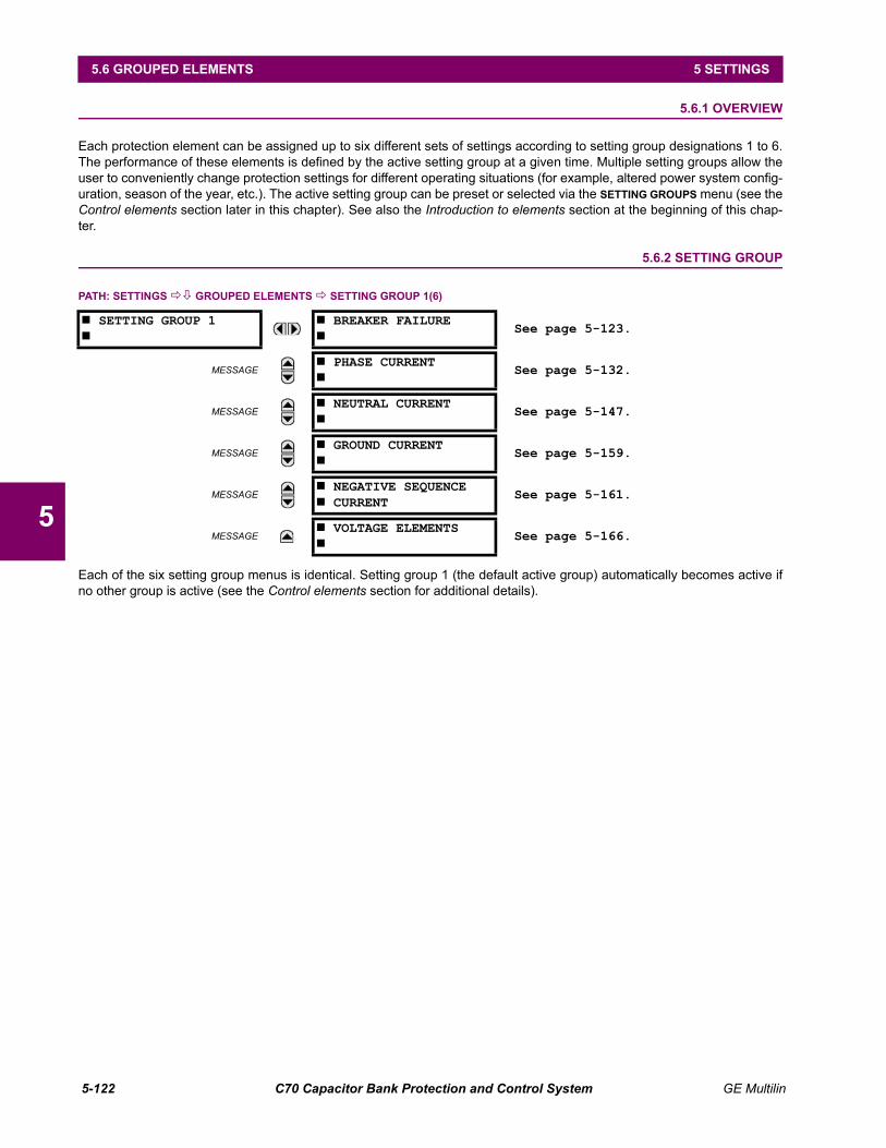
5-122 C70 Capacitor Bank Protection and Control System GE Multilin
5.6 GROUPED ELEMENTS 5 SETTINGS
5
5.6GROUPED ELEMENTS 5.6.1 OVERVIEW
Each protection element can be assigned up to six different sets of settings according to setting group designations 1 to 6.The performance of these elements is defined by the active setting group at a given time. Multiple setting groups allow theuser to conveniently change protection settings for different operating situations (for example, altered power system config-uration, season of the year, etc.). The active setting group can be preset or selected via the SETTING GROUPS menu (see theControl elements section later in this chapter). See also the Introduction to elements section at the beginning of this chap-ter.
5.6.2 SETTING GROUP
PATH: SETTINGS GROUPED ELEMENTS SETTING GROUP 1(6)
Each of the six setting group menus is identical. Setting group 1 (the default active group) automatically becomes active ifno other group is active (see the Control elements section for additional details).
SETTING GROUP 1
BREAKER FAILURE
See page 5-123.
MESSAGE PHASE CURRENT
See page 5-132.
MESSAGE NEUTRAL CURRENT
See page 5-147.
MESSAGE GROUND CURRENT
See page 5-159.
MESSAGE NEGATIVE SEQUENCE CURRENT
See page 5-161.
MESSAGE VOLTAGE ELEMENTS
See page 5-166.

GE Multilin C70 Capacitor Bank Protection and Control System 5-123
5 SETTINGS 5.6 GROUPED ELEMENTS
5
5.6.3 BREAKER FAILURE
PATH: SETTINGS GROUPED ELEMENTS SETTING GROUP 1(6) BREAKER FAILURE BREAKER FAILURE 1
BREAKER FAILURE 1
BF1 FUNCTION:Disabled
Range: Disabled, Enabled
MESSAGEBF1 MODE:3-Pole
Range: 3-Pole, 1-Pole
MESSAGEBF1 SOURCE:SRC 1
Range: SRC 1, SRC 2
MESSAGEBF1 USE AMP SUPV:Yes
Range: Yes, No
MESSAGEBF1 USE SEAL-IN:Yes
Range: Yes, No
MESSAGEBF1 3-POLE INITIATE:Off
Range: FlexLogic operand
MESSAGEBF1 BLOCK:Off
Range: FlexLogic operand
MESSAGEBF1 PH AMP SUPVPICKUP: 1.050 pu
Range: 0.001 to 30.000 pu in steps of 0.001
MESSAGEBF1 N AMP SUPVPICKUP: 1.050 pu
Range: 0.001 to 30.000 pu in steps of 0.001
MESSAGEBF1 USE TIMER 1:Yes
Range: Yes, No
MESSAGEBF1 TIMER 1 PICKUPDELAY: 0.000 s
Range: 0.000 to 65.535 s in steps of 0.001
MESSAGEBF1 USE TIMER 2:Yes
Range: Yes, No
MESSAGEBF1 TIMER 2 PICKUPDELAY: 0.000 s
Range: 0.000 to 65.535 s in steps of 0.001
MESSAGEBF1 USE TIMER 3:Yes
Range: Yes, No
MESSAGEBF1 TIMER 3 PICKUPDELAY: 0.000 s
Range: 0.000 to 65.535 s in steps of 0.001
MESSAGEBF1 BKR POS1 A/3P:Off
Range: FlexLogic operand
MESSAGEBF1 BKR POS2 A/3P:Off
Range: FlexLogic operand
MESSAGEBF1 BREAKER TEST ON:Off
Range: FlexLogic operand
MESSAGEBF1 PH AMP HISETPICKUP: 1.050 pu
Range: 0.001 to 30.000 pu in steps of 0.001
MESSAGEBF1 N AMP HISETPICKUP: 1.050 pu
Range: 0.001 to 30.000 pu in steps of 0.001
MESSAGEBF1 PH AMP LOSETPICKUP: 1.050 pu
Range: 0.001 to 30.000 pu in steps of 0.001

5-124 C70 Capacitor Bank Protection and Control System GE Multilin
5.6 GROUPED ELEMENTS 5 SETTINGS
5
In general, a breaker failure scheme determines that a breaker signaled to trip has not cleared a fault within a definite time,so further tripping action must be performed. Tripping from the breaker failure scheme should trip all breakers, both localand remote, that can supply current to the faulted zone. Usually operation of a breaker failure element will cause clearing ofa larger section of the power system than the initial trip. Because breaker failure can result in tripping a large number ofbreakers and this affects system safety and stability, a very high level of security is required.
Two schemes are provided: one for three-pole tripping only (identified by the name “3BF”) and one for three pole plus sin-gle-pole operation (identified by the name “1BF”). The philosophy used in these schemes is identical. The operation of abreaker failure element includes three stages: initiation, determination of a breaker failure condition, and output.
INITIATION STAGE:
A FlexLogic operand representing the protection trip signal initially sent to the breaker must be selected to initiate thescheme. The initiating signal should be sealed-in if primary fault detection can reset before the breaker failure timers havefinished timing. The seal-in is supervised by current level, so it is reset when the fault is cleared. If desired, an incompletesequence seal-in reset can be implemented by using the initiating operand to also initiate a FlexLogic timer, set longer thanany breaker failure timer, whose output operand is selected to block the breaker failure scheme.
Schemes can be initiated either directly or with current level supervision. It is particularly important in any application todecide if a current-supervised initiate is to be used. The use of a current-supervised initiate results in the breaker failure ele-ment not being initiated for a breaker that has very little or no current flowing through it, which may be the case for trans-former faults. For those situations where it is required to maintain breaker fail coverage for fault levels below the BF1 PH
AMP SUPV PICKUP or the BF1 N AMP SUPV PICKUP setting, a current supervised initiate should not be used. This featureshould be utilized for those situations where coordinating margins may be reduced when high speed reclosing is used.Thus, if this choice is made, fault levels must always be above the supervision pickup levels for dependable operation ofthe breaker fail scheme. This can also occur in breaker-and-a-half or ring bus configurations where the first breaker closesinto a fault; the protection trips and attempts to initiate breaker failure for the second breaker, which is in the process ofclosing, but does not yet have current flowing through it.
MESSAGEBF1 N AMP LOSETPICKUP: 1.050 pu
Range: 0.001 to 30.000 pu in steps of 0.001
MESSAGEBF1 LOSET TIMEDELAY: 0.000 s
Range: 0.000 to 65.535 s in steps of 0.001
MESSAGEBF1 TRIP DROPOUTDELAY: 0.000 s
Range: 0.000 to 65.535 s in steps of 0.001
MESSAGEBF1 TARGETSelf-Reset
Range: Self-reset, Latched, Disabled
MESSAGEBF1 EVENTSDisabled
Range: Disabled, Enabled
MESSAGEBF1 PH A INITIATE:Off
Range: FlexLogic operandValid only for 1-Pole breaker failure schemes.
MESSAGEBF1 PH B INITIATE:Off
Range: FlexLogic operandValid only for 1-Pole breaker failure schemes.
MESSAGEBF1 PH C INITIATE:Off
Range: FlexLogic operandValid only for 1-Pole breaker failure schemes.
MESSAGEBF1 BKR POS1 BOff
Range: FlexLogic operandValid only for 1-Pole breaker failure schemes.
MESSAGEBF1 BKR POS1 COff
Range: FlexLogic operandValid only for 1-Pole breaker failure schemes.
MESSAGEBF1 BKR POS2 BOff
Range: FlexLogic operandValid only for 1-Pole breaker failure schemes.
MESSAGEBF1 BKR POS2 COff
Range: FlexLogic operandValid only for 1-Pole breaker failure schemes.

GE Multilin C70 Capacitor Bank Protection and Control System 5-125
5 SETTINGS 5.6 GROUPED ELEMENTS
5
When the scheme is initiated, it immediately sends a trip signal to the breaker initially signaled to trip (this feature is usuallydescribed as re-trip). This reduces the possibility of widespread tripping that results from a declaration of a failed breaker.
DETERMINATION OF A BREAKER FAILURE CONDITION:
The schemes determine a breaker failure condition via three paths. Each of these paths is equipped with a time delay, afterwhich a failed breaker is declared and trip signals are sent to all breakers required to clear the zone. The delayed paths areassociated with breaker failure timers 1, 2, and 3, which are intended to have delays increasing with increasing timer num-bers. These delayed paths are individually enabled to allow for maximum flexibility.
Timer 1 logic (early path) is supervised by a fast-operating breaker auxiliary contact. If the breaker is still closed (as indi-cated by the auxiliary contact) and fault current is detected after the delay interval, an output is issued. Operation of thebreaker auxiliary switch indicates that the breaker has mechanically operated. The continued presence of current indicatesthat the breaker has failed to interrupt the circuit.
Timer 2 logic (main path) is not supervised by a breaker auxiliary contact. If fault current is detected after the delay interval,an output is issued. This path is intended to detect a breaker that opens mechanically but fails to interrupt fault current; thelogic therefore does not use a breaker auxiliary contact.
The timer 1 and 2 paths provide two levels of current supervision, high-set and low-set, that allow the supervision level tochange from a current which flows before a breaker inserts an opening resistor into the faulted circuit to a lower level afterresistor insertion. The high-set detector is enabled after timeout of timer 1 or 2, along with a timer that will enable the low-set detector after its delay interval. The delay interval between high-set and low-set is the expected breaker opening time.Both current detectors provide a fast operating time for currents at small multiples of the pickup value. The overcurrentdetectors are required to operate after the breaker failure delay interval to eliminate the need for very fast resetting overcur-rent detectors.
Timer 3 logic (slow path) is supervised by a breaker auxiliary contact and a control switch contact used to indicate that thebreaker is in or out-of-service, disabling this path when the breaker is out-of-service for maintenance. There is no currentlevel check in this logic as it is intended to detect low magnitude faults and it is therefore the slowest to operate.
OUTPUT:
The outputs from the schemes are:
• FlexLogic operands that report on the operation of portions of the scheme
• FlexLogic operand used to re-trip the protected breaker
• FlexLogic operands that initiate tripping required to clear the faulted zone. The trip output can be sealed-in for anadjustable period.
• Target message indicating a failed breaker has been declared
• Illumination of the faceplate Trip LED (and the Phase A, B or C LED, if applicable)
MAIN PATH SEQUENCE:
Figure 5–49: BREAKER FAILURE MAIN PATH SEQUENCE
PROTECTION OPERATION BREAKER INTERRUPTING TIME
CALCULATED CURRENT MAGNITUDE
ACTUAL CURRENT MAGNITUDEFAILED INTERRUPTION
CORRECT INTERRUPTION
Rampdown
(ASSUMED 1.5 cycles)
INITIATE (1/8 cycle)BREAKER FAILURE TIMER No. 2 (±1/8 cycle)
BREAKER FAILURE CURRENT DETECTOR PICKUP (1/8 cycle)
BREAKER FAILURE OUTPUT RELAY PICKUP (1/4 cycle)
FAULTOCCURS
1 2 3 4 5 6 7 8 9 10 110
0
0
AMP
(ASSUMED 3 cycles)
cycles
827083A6.CDR
MARGIN(Assumed 2 Cycles)
BACKUP BREAKER OPERATING TIME(Assumed 3 Cycles)

5-126 C70 Capacitor Bank Protection and Control System GE Multilin
5.6 GROUPED ELEMENTS 5 SETTINGS
5
The current supervision elements reset in less than 0.7 of a power cycle for any multiple of pickup current as shown below.
Figure 5–50: BREAKER FAILURE OVERCURRENT SUPERVISION RESET TIME
SETTINGS:
• BF1 MODE: This setting is used to select the breaker failure operating mode: single or three pole.
• BF1 USE AMP SUPV: If set to "Yes", the element will only be initiated if current flowing through the breaker is abovethe supervision pickup level.
• BF1 USE SEAL-IN: If set to "Yes", the element will only be sealed-in if current flowing through the breaker is above thesupervision pickup level.
• BF1 3-POLE INITIATE: This setting selects the FlexLogic operand that will initiate three-pole tripping of the breaker.
• BF1 PH AMP SUPV PICKUP: This setting is used to set the phase current initiation and seal-in supervision level.Generally this setting should detect the lowest expected fault current on the protected breaker. It can be set as low asnecessary (lower than breaker resistor current or lower than load current) – high-set and low-set current supervisionwill guarantee correct operation.
• BF1 N AMP SUPV PICKUP: This setting is used to set the neutral current initiate and seal-in supervision level. Gener-ally this setting should detect the lowest expected fault current on the protected breaker. Neutral current supervision isused only in the three phase scheme to provide increased sensitivity. This setting is valid only for three-pole trippingschemes.
• BF1 USE TIMER 1: If set to "Yes", the early path is operational.
• BF1 TIMER 1 PICKUP DELAY: Timer 1 is set to the shortest time required for breaker auxiliary contact Status-1 toopen, from the time the initial trip signal is applied to the breaker trip circuit, plus a safety margin.
• BF1 USE TIMER 2: If set to "Yes", the main path is operational.
• BF1 TIMER 2 PICKUP DELAY: Timer 2 is set to the expected opening time of the breaker, plus a safety margin. Thissafety margin was historically intended to allow for measuring and timing errors in the breaker failure scheme equip-ment. In microprocessor relays this time is not significant. In C70 relays, which use a Fourier transform, the calculatedcurrent magnitude will ramp-down to zero one power frequency cycle after the current is interrupted, and this lagshould be included in the overall margin duration, as it occurs after current interruption. The Breaker failure main pathsequence diagram below shows a margin of two cycles; this interval is considered the minimum appropriate for mostapplications.
Note that in bulk oil circuit breakers, the interrupting time for currents less than 25% of the interrupting rating can besignificantly longer than the normal interrupting time.
• BF1 USE TIMER 3: If set to "Yes", the Slow Path is operational.
• BF1 TIMER 3 PICKUP DELAY: Timer 3 is set to the same interval as timer 2, plus an increased safety margin.Because this path is intended to operate only for low level faults, the delay can be in the order of 300 to 500 ms.
836769A4.CDR
0
0.2
0.4
0.6
0.8
0 20 40 60 80 100 120 140
Average
Maximum
Margin
Mul ple of pickupfault current
threshold setting
Bre
ake
rfa
ilu
rere
se
tti
me
(cy
cle
s)

GE Multilin C70 Capacitor Bank Protection and Control System 5-127
5 SETTINGS 5.6 GROUPED ELEMENTS
5
• BF1 BKR POS1 A/3P: This setting selects the FlexLogic operand that represents the protected breaker early-typeauxiliary switch contact (52/a). When using the single-pole breaker failure scheme, this operand represents the pro-tected breaker early-type auxiliary switch contact on pole A. This is normally a non-multiplied form-A contact. The con-tact may even be adjusted to have the shortest possible operating time.
• BF1 BKR POS2 A/3P: This setting selects the FlexLogic operand that represents the breaker normal-type auxiliaryswitch contact (52/a). When using the single-pole breaker failure scheme, this operand represents the protectedbreaker auxiliary switch contact on pole A. This may be a multiplied contact.
• BF1 BREAKER TEST ON: This setting is used to select the FlexLogic operand that represents the breaker in-service/out-of-service switch set to the out-of-service position.
• BF1 PH AMP HISET PICKUP: This setting sets the phase current output supervision level. Generally this settingshould detect the lowest expected fault current on the protected breaker, before a breaker opening resistor is inserted.
• BF1 N AMP HISET PICKUP: This setting sets the neutral current output supervision level. Generally this settingshould detect the lowest expected fault current on the protected breaker, before a breaker opening resistor is inserted.Neutral current supervision is used only in the three pole scheme to provide increased sensitivity. This setting is validonly for three-pole breaker failure schemes.
• BF1 PH AMP LOSET PICKUP: This setting sets the phase current output supervision level. Generally this settingshould detect the lowest expected fault current on the protected breaker, after a breaker opening resistor is inserted(approximately 90% of the resistor current).
• BF1 N AMP LOSET PICKUP: This setting sets the neutral current output supervision level. Generally this settingshould detect the lowest expected fault current on the protected breaker, after a breaker opening resistor is inserted(approximately 90% of the resistor current). This setting is valid only for three-pole breaker failure schemes.
• BF1 LOSET TIME DELAY: Sets the pickup delay for current detection after opening resistor insertion.
• BF1 TRIP DROPOUT DELAY: This setting is used to set the period of time for which the trip output is sealed-in. Thistimer must be coordinated with the automatic reclosing scheme of the failed breaker, to which the breaker failure ele-ment sends a cancel reclosure signal. Reclosure of a remote breaker can also be prevented by holding a transfer tripsignal on longer than the reclaim time.
• BF1 PH A INITIATE / BF1 PH B INITIATE / BF 1 PH C INITIATE: These settings select the FlexLogic operand to initi-ate phase A, B, or C single-pole tripping of the breaker and the phase A, B, or C portion of the scheme, accordingly.This setting is only valid for single-pole breaker failure schemes.
• BF1 BKR POS1 B / BF1 BKR POS 1 C: These settings select the FlexLogic operand to represents the protectedbreaker early-type auxiliary switch contact on poles B or C, accordingly. This contact is normally a non-multiplied Form-A contact. The contact may even be adjusted to have the shortest possible operating time. This setting is valid only forsingle-pole breaker failure schemes.
• BF1 BKR POS2 B: Selects the FlexLogic operand that represents the protected breaker normal-type auxiliary switchcontact on pole B (52/a). This may be a multiplied contact. This setting is valid only for single-pole breaker failureschemes.
• BF1 BKR POS2 C: This setting selects the FlexLogic operand that represents the protected breaker normal-typeauxiliary switch contact on pole C (52/a). This may be a multiplied contact. For single-pole operation, the scheme hasthe same overall general concept except that it provides re-tripping of each single pole of the protected breaker. Theapproach shown in the following single pole tripping diagram uses the initiating information to determine which pole issupposed to trip. The logic is segregated on a per-pole basis. The overcurrent detectors have ganged settings. Thissetting is valid only for single-pole breaker failure schemes.
Upon operation of the breaker failure element for a single pole trip command, a three-pole trip command should begiven via output operand BKR FAIL 1 TRIP OP.

5-128 C70 Capacitor Bank Protection and Control System GE Multilin
5.6 GROUPED ELEMENTS 5 SETTINGS
5
Figure 5–51: SINGLE-POLE BREAKER FAILURE, INITIATE
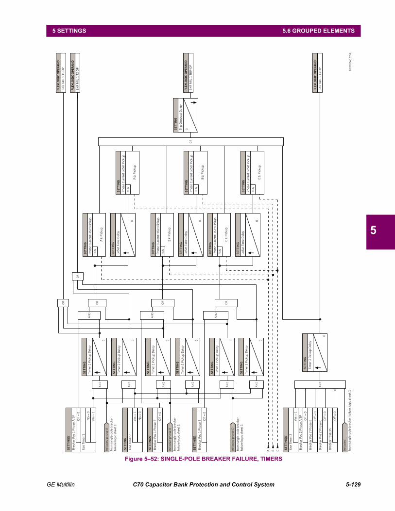
GE Multilin C70 Capacitor Bank Protection and Control System 5-129
5 SETTINGS 5.6 GROUPED ELEMENTS
5
Figure 5–52: SINGLE-POLE BREAKER FAILURE, TIMERS

5-130 C70 Capacitor Bank Protection and Control System GE Multilin
5.6 GROUPED ELEMENTS 5 SETTINGS
5
,
Figure 5–53: THREE-POLE BREAKER FAILURE, INITIATE

GE Multilin C70 Capacitor Bank Protection and Control System 5-131
5 SETTINGS 5.6 GROUPED ELEMENTS
5
Figure 5–54: THREE-POLE BREAKER FAILURE, TIMERS

5-132 C70 Capacitor Bank Protection and Control System GE Multilin
5.6 GROUPED ELEMENTS 5 SETTINGS
5
5.6.4 PHASE CURRENT
a) MAIN MENU
PATH: SETTINGS GROUPED ELEMENTS SETTING GROUP 1(6) PHASE CURRENT
PHASE CURRENT
PHASE TOC1
See page 5–138.
MESSAGE PHASE TOC2
See page 5–138.
MESSAGE PHASE TOC6
See page 5–138.
MESSAGE PHASE IOC1
See page 5–140.
MESSAGE PHASE IOC2
See page 5–140.
MESSAGE PHASE IOC12
See page 5–140.
MESSAGE PHASE DIRECTIONAL 1
See page 5–141.
MESSAGE PHASE DIRECTIONAL 2
See page 5–141.
MESSAGE PHASE CURRENT UNBALANCE 1
See page 5–144.
MESSAGE PHASE CURRENT UNBALANCE 2
See page 5–144.
MESSAGE PHASE CURRENT UNBALANCE 3
See page 5–144.

GE Multilin C70 Capacitor Bank Protection and Control System 5-133
5 SETTINGS 5.6 GROUPED ELEMENTS
5
b) INVERSE TOC CURVE CHARACTERISTICS
The inverse time overcurrent curves used by the time overcurrent elements are the IEEE, IEC, GE Type IAC, and I2t stan-dard curve shapes. This allows for simplified coordination with downstream devices.
If none of these curve shapes is adequate, FlexCurves may be used to customize the inverse time curve characteristics.The definite time curve is also an option that may be appropriate if only simple protection is required.
A time dial multiplier setting allows selection of a multiple of the base curve shape (where the time dial multiplier = 1) withthe curve shape (CURVE) setting. Unlike the electromechanical time dial equivalent, operate times are directly proportionalto the time multiplier (TD MULTIPLIER) setting value. For example, all times for a multiplier of 10 are 10 times the multiplier 1or base curve values. Setting the multiplier to zero results in an instantaneous response to all current levels above pickup.
Time overcurrent time calculations are made with an internal energy capacity memory variable. When this variable indi-cates that the energy capacity has reached 100%, a time overcurrent element will operate. If less than 100% energy capac-ity is accumulated in this variable and the current falls below the dropout threshold of 97 to 98% of the pickup value, thevariable must be reduced. Two methods of this resetting operation are available: “Instantaneous” and “Timed”. The “Instan-taneous” selection is intended for applications with other relays, such as most static relays, which set the energy capacitydirectly to zero when the current falls below the reset threshold. The “Timed” selection can be used where the relay mustcoordinate with electromechanical relays.
IEEE CURVES:
The IEEE time overcurrent curve shapes conform to industry standards and the IEEE C37.112-1996 curve classificationsfor extremely, very, and moderately inverse. The IEEE curves are derived from the formulae:
, (EQ 5.7)
where: T = operate time (in seconds), TDM = Multiplier setting, I = input current, Ipickup = Pickup Current settingA, B, p = constants, TRESET = reset time in seconds (assuming energy capacity is 100% and RESET is “Timed”),tr = characteristic constant
Table 5–12: OVERCURRENT CURVE TYPES
IEEE IEC GE TYPE IAC OTHER
IEEE Extremely Inverse IEC Curve A (BS142) IAC Extremely Inverse I2t
IEEE Very Inverse IEC Curve B (BS142) IAC Very Inverse FlexCurves A, B, C, and D
IEEE Moderately Inverse IEC Curve C (BS142) IAC Inverse Recloser Curves
IEC Short Inverse IAC Short Inverse Definite Time
Table 5–13: IEEE INVERSE TIME CURVE CONSTANTS
IEEE CURVE SHAPE A B P TR
IEEE Extremely Inverse 28.2 0.1217 2.0000 29.1
IEEE Very Inverse 19.61 0.491 2.0000 21.6
IEEE Moderately Inverse 0.0515 0.1140 0.02000 4.85
Table 5–14: IEEE CURVE TRIP TIMES (IN SECONDS)
MULTIPLIER(TDM)
CURRENT ( I / Ipickup)
1.5 2.0 3.0 4.0 5.0 6.0 7.0 8.0 9.0 10.0
IEEE EXTREMELY INVERSE
0.5 11.341 4.761 1.823 1.001 0.648 0.464 0.355 0.285 0.237 0.203
1.0 22.682 9.522 3.647 2.002 1.297 0.927 0.709 0.569 0.474 0.407
2.0 45.363 19.043 7.293 4.003 2.593 1.855 1.418 1.139 0.948 0.813
4.0 90.727 38.087 14.587 8.007 5.187 3.710 2.837 2.277 1.897 1.626
6.0 136.090 57.130 21.880 12.010 7.780 5.564 4.255 3.416 2.845 2.439
8.0 181.454 76.174 29.174 16.014 10.374 7.419 5.674 4.555 3.794 3.252
T TDM
AI
Ipickup---------------- p
1–---------------------------------- B+
= TRESET TDM
tr
1I
Ipickup----------------
2–
------------------------------------=

5-134 C70 Capacitor Bank Protection and Control System GE Multilin
5.6 GROUPED ELEMENTS 5 SETTINGS
5
10.0 226.817 95.217 36.467 20.017 12.967 9.274 7.092 5.693 4.742 4.065
IEEE VERY INVERSE
0.5 8.090 3.514 1.471 0.899 0.654 0.526 0.450 0.401 0.368 0.345
1.0 16.179 7.028 2.942 1.798 1.308 1.051 0.900 0.802 0.736 0.689
2.0 32.358 14.055 5.885 3.597 2.616 2.103 1.799 1.605 1.472 1.378
4.0 64.716 28.111 11.769 7.193 5.232 4.205 3.598 3.209 2.945 2.756
6.0 97.074 42.166 17.654 10.790 7.849 6.308 5.397 4.814 4.417 4.134
8.0 129.432 56.221 23.538 14.387 10.465 8.410 7.196 6.418 5.889 5.513
10.0 161.790 70.277 29.423 17.983 13.081 10.513 8.995 8.023 7.361 6.891
IEEE MODERATELY INVERSE
0.5 3.220 1.902 1.216 0.973 0.844 0.763 0.706 0.663 0.630 0.603
1.0 6.439 3.803 2.432 1.946 1.688 1.526 1.412 1.327 1.260 1.207
2.0 12.878 7.606 4.864 3.892 3.377 3.051 2.823 2.653 2.521 2.414
4.0 25.756 15.213 9.729 7.783 6.753 6.102 5.647 5.307 5.041 4.827
6.0 38.634 22.819 14.593 11.675 10.130 9.153 8.470 7.960 7.562 7.241
8.0 51.512 30.426 19.458 15.567 13.507 12.204 11.294 10.614 10.083 9.654
10.0 64.390 38.032 24.322 19.458 16.883 15.255 14.117 13.267 12.604 12.068
Table 5–14: IEEE CURVE TRIP TIMES (IN SECONDS)
MULTIPLIER(TDM)
CURRENT ( I / Ipickup)
1.5 2.0 3.0 4.0 5.0 6.0 7.0 8.0 9.0 10.0
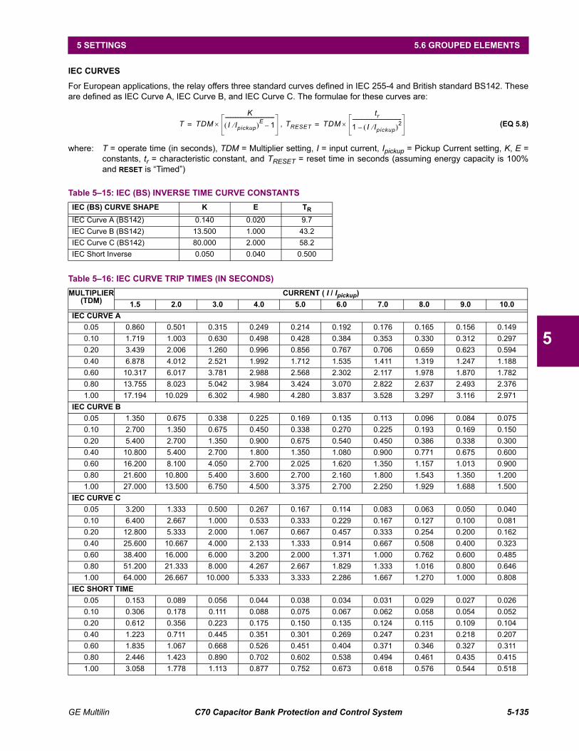
GE Multilin C70 Capacitor Bank Protection and Control System 5-135
5 SETTINGS 5.6 GROUPED ELEMENTS
5
IEC CURVES
For European applications, the relay offers three standard curves defined in IEC 255-4 and British standard BS142. Theseare defined as IEC Curve A, IEC Curve B, and IEC Curve C. The formulae for these curves are:
, (EQ 5.8)
where: T = operate time (in seconds), TDM = Multiplier setting, I = input current, Ipickup = Pickup Current setting, K, E =constants, tr = characteristic constant, and TRESET = reset time in seconds (assuming energy capacity is 100%and RESET is “Timed”)
Table 5–15: IEC (BS) INVERSE TIME CURVE CONSTANTS
IEC (BS) CURVE SHAPE K E TR
IEC Curve A (BS142) 0.140 0.020 9.7
IEC Curve B (BS142) 13.500 1.000 43.2
IEC Curve C (BS142) 80.000 2.000 58.2
IEC Short Inverse 0.050 0.040 0.500
Table 5–16: IEC CURVE TRIP TIMES (IN SECONDS)
MULTIPLIER(TDM)
CURRENT ( I / Ipickup)
1.5 2.0 3.0 4.0 5.0 6.0 7.0 8.0 9.0 10.0
IEC CURVE A
0.05 0.860 0.501 0.315 0.249 0.214 0.192 0.176 0.165 0.156 0.149
0.10 1.719 1.003 0.630 0.498 0.428 0.384 0.353 0.330 0.312 0.297
0.20 3.439 2.006 1.260 0.996 0.856 0.767 0.706 0.659 0.623 0.594
0.40 6.878 4.012 2.521 1.992 1.712 1.535 1.411 1.319 1.247 1.188
0.60 10.317 6.017 3.781 2.988 2.568 2.302 2.117 1.978 1.870 1.782
0.80 13.755 8.023 5.042 3.984 3.424 3.070 2.822 2.637 2.493 2.376
1.00 17.194 10.029 6.302 4.980 4.280 3.837 3.528 3.297 3.116 2.971
IEC CURVE B
0.05 1.350 0.675 0.338 0.225 0.169 0.135 0.113 0.096 0.084 0.075
0.10 2.700 1.350 0.675 0.450 0.338 0.270 0.225 0.193 0.169 0.150
0.20 5.400 2.700 1.350 0.900 0.675 0.540 0.450 0.386 0.338 0.300
0.40 10.800 5.400 2.700 1.800 1.350 1.080 0.900 0.771 0.675 0.600
0.60 16.200 8.100 4.050 2.700 2.025 1.620 1.350 1.157 1.013 0.900
0.80 21.600 10.800 5.400 3.600 2.700 2.160 1.800 1.543 1.350 1.200
1.00 27.000 13.500 6.750 4.500 3.375 2.700 2.250 1.929 1.688 1.500
IEC CURVE C
0.05 3.200 1.333 0.500 0.267 0.167 0.114 0.083 0.063 0.050 0.040
0.10 6.400 2.667 1.000 0.533 0.333 0.229 0.167 0.127 0.100 0.081
0.20 12.800 5.333 2.000 1.067 0.667 0.457 0.333 0.254 0.200 0.162
0.40 25.600 10.667 4.000 2.133 1.333 0.914 0.667 0.508 0.400 0.323
0.60 38.400 16.000 6.000 3.200 2.000 1.371 1.000 0.762 0.600 0.485
0.80 51.200 21.333 8.000 4.267 2.667 1.829 1.333 1.016 0.800 0.646
1.00 64.000 26.667 10.000 5.333 3.333 2.286 1.667 1.270 1.000 0.808
IEC SHORT TIME
0.05 0.153 0.089 0.056 0.044 0.038 0.034 0.031 0.029 0.027 0.026
0.10 0.306 0.178 0.111 0.088 0.075 0.067 0.062 0.058 0.054 0.052
0.20 0.612 0.356 0.223 0.175 0.150 0.135 0.124 0.115 0.109 0.104
0.40 1.223 0.711 0.445 0.351 0.301 0.269 0.247 0.231 0.218 0.207
0.60 1.835 1.067 0.668 0.526 0.451 0.404 0.371 0.346 0.327 0.311
0.80 2.446 1.423 0.890 0.702 0.602 0.538 0.494 0.461 0.435 0.415
1.00 3.058 1.778 1.113 0.877 0.752 0.673 0.618 0.576 0.544 0.518
T TDM
K
I Ipickup E 1–---------------------------------------
= TRESET TDM
tr
1 I Ipickup 2–---------------------------------------
=

5-136 C70 Capacitor Bank Protection and Control System GE Multilin
5.6 GROUPED ELEMENTS 5 SETTINGS
5
IAC CURVES:
The curves for the General Electric type IAC relay family are derived from the formulae:
, (EQ 5.9)
where: T = operate time (in seconds), TDM = Multiplier setting, I = Input current, Ipkp = Pickup Current setting, A to E =constants, tr = characteristic constant, and TRESET = reset time in seconds (assuming energy capacity is 100%and RESET is “Timed”)
Table 5–17: GE TYPE IAC INVERSE TIME CURVE CONSTANTS
IAC CURVE SHAPE A B C D E TR
IAC Extreme Inverse 0.0040 0.6379 0.6200 1.7872 0.2461 6.008
IAC Very Inverse 0.0900 0.7955 0.1000 –1.2885 7.9586 4.678
IAC Inverse 0.2078 0.8630 0.8000 –0.4180 0.1947 0.990
IAC Short Inverse 0.0428 0.0609 0.6200 –0.0010 0.0221 0.222
Table 5–18: IAC CURVE TRIP TIMES
MULTIPLIER(TDM)
CURRENT ( I / Ipickup)
1.5 2.0 3.0 4.0 5.0 6.0 7.0 8.0 9.0 10.0
IAC EXTREMELY INVERSE
0.5 1.699 0.749 0.303 0.178 0.123 0.093 0.074 0.062 0.053 0.046
1.0 3.398 1.498 0.606 0.356 0.246 0.186 0.149 0.124 0.106 0.093
2.0 6.796 2.997 1.212 0.711 0.491 0.372 0.298 0.248 0.212 0.185
4.0 13.591 5.993 2.423 1.422 0.983 0.744 0.595 0.495 0.424 0.370
6.0 20.387 8.990 3.635 2.133 1.474 1.115 0.893 0.743 0.636 0.556
8.0 27.183 11.987 4.846 2.844 1.966 1.487 1.191 0.991 0.848 0.741
10.0 33.979 14.983 6.058 3.555 2.457 1.859 1.488 1.239 1.060 0.926
IAC VERY INVERSE
0.5 1.451 0.656 0.269 0.172 0.133 0.113 0.101 0.093 0.087 0.083
1.0 2.901 1.312 0.537 0.343 0.266 0.227 0.202 0.186 0.174 0.165
2.0 5.802 2.624 1.075 0.687 0.533 0.453 0.405 0.372 0.349 0.331
4.0 11.605 5.248 2.150 1.374 1.065 0.906 0.810 0.745 0.698 0.662
6.0 17.407 7.872 3.225 2.061 1.598 1.359 1.215 1.117 1.046 0.992
8.0 23.209 10.497 4.299 2.747 2.131 1.813 1.620 1.490 1.395 1.323
10.0 29.012 13.121 5.374 3.434 2.663 2.266 2.025 1.862 1.744 1.654
IAC INVERSE
0.5 0.578 0.375 0.266 0.221 0.196 0.180 0.168 0.160 0.154 0.148
1.0 1.155 0.749 0.532 0.443 0.392 0.360 0.337 0.320 0.307 0.297
2.0 2.310 1.499 1.064 0.885 0.784 0.719 0.674 0.640 0.614 0.594
4.0 4.621 2.997 2.128 1.770 1.569 1.439 1.348 1.280 1.229 1.188
6.0 6.931 4.496 3.192 2.656 2.353 2.158 2.022 1.921 1.843 1.781
8.0 9.242 5.995 4.256 3.541 3.138 2.878 2.695 2.561 2.457 2.375
10.0 11.552 7.494 5.320 4.426 3.922 3.597 3.369 3.201 3.072 2.969
IAC SHORT INVERSE
0.5 0.072 0.047 0.035 0.031 0.028 0.027 0.026 0.026 0.025 0.025
1.0 0.143 0.095 0.070 0.061 0.057 0.054 0.052 0.051 0.050 0.049
2.0 0.286 0.190 0.140 0.123 0.114 0.108 0.105 0.102 0.100 0.099
4.0 0.573 0.379 0.279 0.245 0.228 0.217 0.210 0.204 0.200 0.197
6.0 0.859 0.569 0.419 0.368 0.341 0.325 0.314 0.307 0.301 0.296
8.0 1.145 0.759 0.559 0.490 0.455 0.434 0.419 0.409 0.401 0.394
10.0 1.431 0.948 0.699 0.613 0.569 0.542 0.524 0.511 0.501 0.493
T TDM AB
I Ipkp C–------------------------------
D
I Ipkp C– 2--------------------------------------
E
I Ipkp C– 3--------------------------------------+ + +
= TRESET TDMtr
1 I Ipkp 2–--------------------------------=
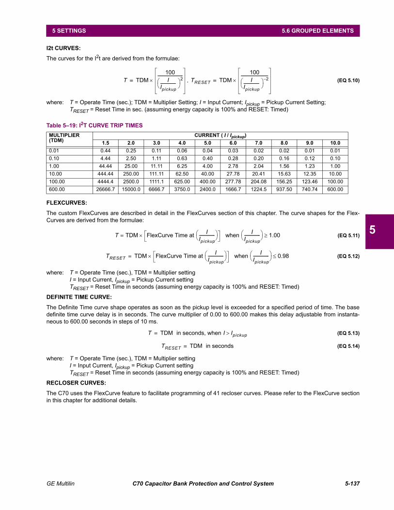
GE Multilin C70 Capacitor Bank Protection and Control System 5-137
5 SETTINGS 5.6 GROUPED ELEMENTS
5
I2t CURVES:
The curves for the I2t are derived from the formulae:
, (EQ 5.10)
where: T = Operate Time (sec.); TDM = Multiplier Setting; I = Input Current; Ipickup = Pickup Current Setting;TRESET = Reset Time in sec. (assuming energy capacity is 100% and RESET: Timed)
FLEXCURVES:
The custom FlexCurves are described in detail in the FlexCurves section of this chapter. The curve shapes for the Flex-Curves are derived from the formulae:
(EQ 5.11)
(EQ 5.12)
where: T = Operate Time (sec.), TDM = Multiplier settingI = Input Current, Ipickup = Pickup Current settingTRESET = Reset Time in seconds (assuming energy capacity is 100% and RESET: Timed)
DEFINITE TIME CURVE:
The Definite Time curve shape operates as soon as the pickup level is exceeded for a specified period of time. The basedefinite time curve delay is in seconds. The curve multiplier of 0.00 to 600.00 makes this delay adjustable from instanta-neous to 600.00 seconds in steps of 10 ms.
(EQ 5.13)
(EQ 5.14)
where: T = Operate Time (sec.), TDM = Multiplier settingI = Input Current, Ipickup = Pickup Current settingTRESET = Reset Time in seconds (assuming energy capacity is 100% and RESET: Timed)
RECLOSER CURVES:
The C70 uses the FlexCurve feature to facilitate programming of 41 recloser curves. Please refer to the FlexCurve sectionin this chapter for additional details.
Table 5–19: I2T CURVE TRIP TIMES
MULTIPLIER(TDM)
CURRENT ( I / Ipickup)
1.5 2.0 3.0 4.0 5.0 6.0 7.0 8.0 9.0 10.0
0.01 0.44 0.25 0.11 0.06 0.04 0.03 0.02 0.02 0.01 0.01
0.10 4.44 2.50 1.11 0.63 0.40 0.28 0.20 0.16 0.12 0.10
1.00 44.44 25.00 11.11 6.25 4.00 2.78 2.04 1.56 1.23 1.00
10.00 444.44 250.00 111.11 62.50 40.00 27.78 20.41 15.63 12.35 10.00
100.00 4444.4 2500.0 1111.1 625.00 400.00 277.78 204.08 156.25 123.46 100.00
600.00 26666.7 15000.0 6666.7 3750.0 2400.0 1666.7 1224.5 937.50 740.74 600.00
T TDM100I
Ipickup---------------- 2--------------------------
= TRESET TDM100I
Ipickup---------------- 2–----------------------------
=
T TDM FlexCurve Time at I
Ipickup---------------- = when
IIpickup---------------- 1.00
TRESET TDM FlexCurve Time at I
Ipickup---------------- when
IIpickup---------------- 0.98=
T TDM in seconds, when I Ipickup=
TRESET TDM in seconds=

5-138 C70 Capacitor Bank Protection and Control System GE Multilin
5.6 GROUPED ELEMENTS 5 SETTINGS
5
c) PHASE TIME OVERCURRENT (ANSI 51P, IEC PTOC)
PATH: SETTINGS GROUPED ELEMENTS SETTING GROUP 1(6) PHASE CURRENT PHASE TOC1(6)
The phase time overcurrent element can provide a desired time-delay operating characteristic versus the applied current orbe used as a simple definite time element. The phase current input quantities may be programmed as fundamental phasormagnitude or total waveform RMS magnitude as required by the application.
Two methods of resetting operation are available: “Timed” and “Instantaneous” (refer to the Inverse Time overcurrentcurves characteristic sub-section earlier for details on curve setup, trip times, and reset operation). When the element isblocked, the time accumulator will reset according to the reset characteristic. For example, if the element reset characteris-tic is set to “Instantaneous” and the element is blocked, the time accumulator will be cleared immediately.
The PHASE TOC1 PICKUP setting can be dynamically reduced by a voltage restraint feature (when enabled). This is accom-plished via the multipliers (Mvr) corresponding to the phase-phase voltages of the voltage restraint characteristic curve (seethe figure below); the pickup level is calculated as ‘Mvr’ times the PHASE TOC1 PICKUP setting. If the voltage restraint featureis disabled, the pickup level always remains at the setting value.
PHASE TOC1
PHASE TOC1FUNCTION: Disabled
Range: Disabled, Enabled
MESSAGEPHASE TOC1 SIGNALSOURCE: SRC 1
Range: SRC 1, SRC 2
MESSAGEPHASE TOC1INPUT: Phasor
Range: Phasor, RMS
MESSAGEPHASE TOC1PICKUP: 1.000 pu
Range: 0.000 to 30.000 pu in steps of 0.001
MESSAGEPHASE TOC1CURVE: IEEE Mod Inv
Range: See Overcurrent Curve Types table
MESSAGEPHASE TOC1TD MULTIPLIER: 1.00
Range: 0.00 to 600.00 in steps of 0.01
MESSAGEPHASE TOC1RESET: Instantaneous
Range: Instantaneous, Timed
MESSAGEPHASE TOC1 VOLTAGERESTRAINT: Disabled
Range: Disabled, Enabled
MESSAGEPHASE TOC1 BLOCK A:Off
Range: FlexLogic operand
MESSAGEPHASE TOC1 BLOCK B:Off
Range: FlexLogic operand
MESSAGEPHASE TOC1 BLOCK C:Off
Range: FlexLogic operand
MESSAGEPHASE TOC1TARGET: Self-reset
Range: Self-reset, Latched, Disabled
MESSAGEPHASE TOC1EVENTS: Disabled
Range: Disabled, Enabled

GE Multilin C70 Capacitor Bank Protection and Control System 5-139
5 SETTINGS 5.6 GROUPED ELEMENTS
5
Figure 5–55: PHASE TIME OVERCURRENT VOLTAGE RESTRAINT CHARACTERISTIC
Figure 5–56: PHASE TIME OVERCURRENT 1 SCHEME LOGIC
0.1
0.2
0.3
0.4
0.5
0.6
0.7
0.8
0.9
1.0
0.1 0.2 0.3 0.4 0.5 0.6 0.7 0.8 0.9 1.00
818784A4.CDR
Mu
ltip
lie
rfo
rP
ick
up
Cu
rre
nt
Phase-Phase Voltage ÷ VT Nominal Phase-phase Voltage
SETTING
SETTING
SETTING
SETTING
SETTING
MULTIPLY INPUTS
FLEXLOGIC OPERAND
SETTING
PHASE TOC1FUNCTION:
PHASE TOC1BLOCK-A :
PHASE TOC1BLOCK-C:
PHASE TOC1BLOCK-B:
PHASE TOC1 VOLTRESTRAINT:
PHASE TOC1 A PKP
PHASE TOC1 A DPO
PHASE TOC1 A OP
PHASE TOC1 B PKP
PHASE TOC1 B DPO
PHASE TOC1 B OP
PHASE TOC1 C PKP
PHASE TOC1 C DPO
PHASE TOC1 C OP
PHASE TOC1 PKP
PHASE TOC1 OP
PHASE TOC1SOURCE:
PHASE TOC1RESET:
PHASE TOC1CURVE:
PHASE TOC1PICKUP:
PHASE TOC1INPUT:
IA
Seq=ABC Seq=ACB
SetMultiplier
SetMultiplier
SetMultiplier
Set PickupMultiplier-Phase A
Calculate
Calculate
Calculate
Set PickupMultiplier-Phase B
Set PickupMultiplier-Phase C
RUN
IB
VAB VAC
RUN
IC
VBC VBA
VCA VCBRUN
Off=0
Off=0
Off=0
Enabled
Enabled=1
Disabled=0
OR
AND
AND
AND
OR
827072A4.CDR
PHASE TOC1TD MULTIPLIER:
RUN
RUN
RUN
IA PICKUP
t
t
t
IB PICKUP
IC PICKUP
SETTING
PHASE TOC1 DPOAND

5-140 C70 Capacitor Bank Protection and Control System GE Multilin
5.6 GROUPED ELEMENTS 5 SETTINGS
5
d) PHASE INSTANTANEOUS OVERCURRENT (ANSI 50P, IEC PIOC)
PATH: SETTINGS GROUPED ELEMENTS SETTING GROUP 1(6) PHASE CURRENT PHASE IOC 1(12)
The phase instantaneous overcurrent element may be used as an instantaneous element with no intentional delay or as adefinite time element. The input current is the fundamental phasor magnitude. For timing curves, see the publication Instan-taneous Overcurrent Element Response to Saturated Waveforms in UR-Series Relays (GET-8400A).
Figure 5–57: PHASE INSTANTANEOUS OVERCURRENT 1 SCHEME LOGIC
PHASE IOC1
PHASE IOC1FUNCTION: Disabled
Range: Disabled, Enabled
MESSAGEPHASE IOC1 SIGNALSOURCE: SRC 1
Range: SRC 1, SRC 2
MESSAGEPHASE IOC1PICKUP: 1.000 pu
Range: 0.000 to 30.000 pu in steps of 0.001
MESSAGEPHASE IOC1 PICKUPDELAY: 0.00 s
Range: 0.00 to 600.00 s in steps of 0.01
MESSAGEPHASE IOC1 RESETDELAY: 0.00 s
Range: 0.00 to 600.00 s in steps of 0.01
MESSAGEPHASE IOC1 BLOCK A:Off
Range: FlexLogic operand
MESSAGEPHASE IOC1 BLOCK B:Off
Range: FlexLogic operand
MESSAGEPHASE IOC1 BLOCK C:Off
Range: FlexLogic operand
MESSAGEPHASE IOC1TARGET: Self-reset
Range: Self-reset, Latched, Disabled
MESSAGEPHASE IOC1EVENTS: Disabled
Range: Disabled, Enabled
IA ≥ PICKUP
SETTING
PHASE IOC1
FUNCTION:
Enabled = 1
Disabled = 0
SETTING
PHASE IOC1
SOURCE:
IA
IB
IC
PHASE IOC1
BLOCK-A:
Off = 0
SETTING
SETTING
IB ≥ PICKUP
RUN
PHASE IOC1
PICKUP:
RUN
IC ≥ PICKUP
RUN
PHASE IOC1
PICKUPDELAY:
SETTINGS
PHASE IOC1 RESET
DELAY:
tPKP
tRST
tPKP
tRST
tPKP
tRST
827033A6.VSD
FLEXLOGIC
OPERANDS
PHASE IOC1 B PKP
PHASE IOC1 B DPO
PHASE IOC1 PKP
PHASE IOC1 C PKP
PHASE IOC1 C DPO
PHASE IOC1 A OP
PHASE IOC1 B OP
PHASE IOC1 OP
OR
AND
OR
AND
AND
PHASE IOC1 A DPO
PHASE IOC1 A PKP
PHASE IOC1 C OP
PHASE IOC1
BLOCK-B:
Off = 0
SETTING
PHASE IOC1
BLOCK-C:
Off = 0
SETTING
PHASE IOC1 DPOAND
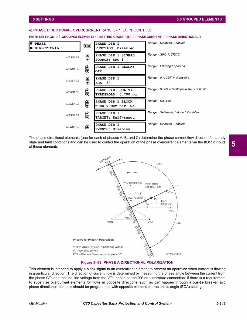
GE Multilin C70 Capacitor Bank Protection and Control System 5-141
5 SETTINGS 5.6 GROUPED ELEMENTS
5
e) PHASE DIRECTIONAL OVERCURRENT (ANSI 67P, IEC PDOC/PTOC)
PATH: SETTINGS GROUPED ELEMENTS SETTING GROUP 1(6) PHASE CURRENT PHASE DIRECTIONAL 1
The phase directional elements (one for each of phases A, B, and C) determine the phase current flow direction for steadystate and fault conditions and can be used to control the operation of the phase overcurrent elements via the BLOCK inputsof these elements.
Figure 5–58: PHASE A DIRECTIONAL POLARIZATION
This element is intended to apply a block signal to an overcurrent element to prevent an operation when current is flowingin a particular direction. The direction of current flow is determined by measuring the phase angle between the current fromthe phase CTs and the line-line voltage from the VTs, based on the 90° or quadrature connection. If there is a requirementto supervise overcurrent elements for flows in opposite directions, such as can happen through a bus-tie breaker, twophase directional elements should be programmed with opposite element characteristic angle (ECA) settings.
PHASE DIRECTIONAL 1
PHASE DIR 1FUNCTION: Disabled
Range: Disabled, Enabled
MESSAGEPHASE DIR 1 SIGNALSOURCE: SRC 1
Range: SRC 1, SRC 2
MESSAGEPHASE DIR 1 BLOCK:Off
Range: FlexLogic operand
MESSAGEPHASE DIR 1ECA: 30
Range: 0 to 359° in steps of 1
MESSAGEPHASE DIR POL V1THRESHOLD: 0.700 pu
Range: 0.000 to 3.000 pu in steps of 0.001
MESSAGEPHASE DIR 1 BLOCKWHEN V MEM EXP: No
Range: No, Yes
MESSAGEPHASE DIR 1TARGET: Self-reset
Range: Self-reset, Latched, Disabled
MESSAGEPHASE DIR 1EVENTS: Disabled
Range: Disabled, Enabled
827800A2.CDR
VBGVCG
VAG(Faulted) IAECAset at 30°
ECA = Element Characteristic Angle at 30°
IA = operating current
Phasors for Phase A Polarization:
VPol = VBC (1/_ECA) = polarizing voltage×
Fault angle
set at 60° Lag
VAG (Unfaulted)
OUTPUTS0
1
VBC
VBC
VPol
+90°
–90°

5-142 C70 Capacitor Bank Protection and Control System GE Multilin
5.6 GROUPED ELEMENTS 5 SETTINGS
5
To increase security for three phase faults very close to the VTs used to measure the polarizing voltage, a voltage memoryfeature is incorporated. This feature stores the polarizing voltage the moment before the voltage collapses, and uses it todetermine direction. The voltage memory remains valid for one second after the voltage has collapsed.
The main component of the phase directional element is the phase angle comparator with two inputs: the operating signal(phase current) and the polarizing signal (the line voltage, shifted in the leading direction by the characteristic angle, ECA).
The following table shows the operating and polarizing signals used for phase directional control:
MODE OF OPERATION:
• When the function is “Disabled”, or the operating current is below 5% CT nominal, the element output is “0”.
• When the function is “Enabled”, the operating current is above 5% CT nominal, and the polarizing voltage is abovethe PRODUCT SETUP DISPLAY PROPERTIES VOLTAGE CUT-OFF LEVEL value, the element output is dependent onthe phase angle between the operating and polarizing signals:
– The element output is logic “0” when the operating current is within polarizing voltage ±90°.– For all other angles, the element output is logic “1”.
• Once the voltage memory has expired, the phase overcurrent elements under directional control can be set to block ortrip on overcurrent as follows:
– When BLOCK WHEN V MEM EXP is set to “Yes”, the directional element will block the operation of any phaseovercurrent element under directional control when voltage memory expires.
– When BLOCK WHEN V MEM EXP is set to “No”, the directional element allows tripping of phase overcurrent elementsunder directional control when voltage memory expires.
In all cases, directional blocking will be permitted to resume when the polarizing voltage becomes greater than the ‘polariz-ing voltage threshold’.
SETTINGS:
• PHASE DIR 1 SIGNAL SOURCE: This setting is used to select the source for the operating and polarizing signals.The operating current for the phase directional element is the phase current for the selected current source. The polar-izing voltage is the line voltage from the phase VTs, based on the 90° or ‘quadrature’ connection and shifted in theleading direction by the element characteristic angle (ECA).
• PHASE DIR 1 ECA: This setting is used to select the element characteristic angle, i.e. the angle by which the polariz-ing voltage is shifted in the leading direction to achieve dependable operation. In the design of the UR-series elements,a block is applied to an element by asserting logic 1 at the blocking input. This element should be programmed via theECA setting so that the output is logic 1 for current in the non-tripping direction.
• PHASE DIR 1 POL V THRESHOLD: This setting is used to establish the minimum level of voltage for which the phaseangle measurement is reliable. The setting is based on VT accuracy. The default value is “0.700 pu”.
• PHASE DIR 1 BLOCK WHEN V MEM EXP: This setting is used to select the required operation upon expiration ofvoltage memory. When set to "Yes", the directional element blocks the operation of any phase overcurrent elementunder directional control, when voltage memory expires; when set to "No", the directional element allows tripping ofphase overcurrent elements under directional control.
The phase directional element responds to the forward load current. In the case of a following reverse fault, the ele-ment needs some time – in the order of 8 ms – to establish a blocking signal. Some protection elements such asinstantaneous overcurrent may respond to reverse faults before the blocking signal is established. Therefore, acoordination time of at least 10 ms must be added to all the instantaneous protection elements under the supervi-sion of the phase directional element. If current reversal is of a concern, a longer delay – in the order of 20 ms –may be needed.
PHASE OPERATINGSIGNAL
POLARIZING SIGNAL Vpol
ABC PHASE SEQUENCE ACB PHASE SEQUENCE
A angle of IA angle of VBC (1ECA) angle of VCB (1ECA)
B angle of IB angle of VCA (1ECA) angle of VAC 1ECA)
C angle of IC angle of VAB (1ECA) angle of VBA (1ECA)
NOTE

GE Multilin C70 Capacitor Bank Protection and Control System 5-143
5 SETTINGS 5.6 GROUPED ELEMENTS
5
Figure 5–59: PHASE DIRECTIONAL SCHEME LOGIC
FLEXLOGIC OPERAND
FLEXLOGIC OPERAND
FLEXLOGIC OPERAND
FLEXLOGIC OPERAND
SETTING
SETTING
SETTING
SETTING
SETTING
SETTING
PHASE DIR 1FUNCTION:
PHASE DIR 1 SOURCE:
PHASE DIR 1 BLOCK OCWHEN V MEM EXP:
PHASE DIR 1BLOCK:
PHASE DIR 1 ECA:
PHASE DIR 1 POL VTHRESHOLD:
PH DIR1 BLK A
PH DIR1 BLK B
PH DIR1 BLK C
PH DIR1 BLK
Disabled=0
IA
No
Seq=ABC Seq=ACB
Yes
VBC VCB
827078A6.CDR
Off=0
V MINIMUM
-Use V when V Min-Use V memory when
V < Min
I 0.05 pu
Enabled=1
AND
AND
OR
MEMORY TIMER
1 cycle1 sec
Vpol
0
I1
RUNAND
PHASE B LOGIC SIMILAR TO PHASE A
PHASE C LOGIC SIMILAR TO PHASE A
OR
USE ACTUAL VOLTAGE
USE MEMORIZED VOLTAGE

5-144 C70 Capacitor Bank Protection and Control System GE Multilin
5.6 GROUPED ELEMENTS 5 SETTINGS
5
f) PHASE CURRENT UNBALANCE (ANSI 60P, IEC PVCB/PTOC)
PATH: SETTINGS GROUPED ELEMENTS SETTING GROUP 1(6) PHASE CURRENT PHASE CURRENT UNBALANCE 1(3)
PHASE CURRENT UNBALANCE 1
CUR UNBALCE 1FUNCTION: Disabled
Range: Disabled, Enabled
MESSAGECUR UNBALCE 1 DIFSOURCE: SRC 1
Range: SRC 1, SRC 2, SRC 3, SRC 4, SRC 5, SRC 6
MESSAGECUR UNBALCE 1 BANKSOURCE: SRC 1
Range: SRC 1, SRC 2, SRC 3, SRC 4, SRC 5, SRC 6
MESSAGECUR UNBALCE 1 INHNTFACTOR A: 0.0000
Range: –0.1000 to 0.1000 in steps of 0.0001
MESSAGECUR UNBALCE 1 INHNTFACTOR B: 0.0000
Range: –0.1000 to 0.1000 in steps of 0.0001
MESSAGECUR UNBALCE 1 INHNTFACTOR C: 0.0000
Range: –0.1000 to 0.1000 in steps of 0.0001
MESSAGECUR UNBALCE 1 STG 1APICKUP: 0.020 pu
Range: 0.001 to 5.000 pu in steps of 0.001
MESSAGECUR UNBALCE 1 STG 2APICKUP: 0.030 pu
Range: 0.001 to 5.000 pu in steps of 0.001
MESSAGECUR UNBALCE 1 STG 3APICKUP: 0.040 pu
Range: 0.001 to 5.000 pu in steps of 0.001
MESSAGECUR UNBALCE 1 STG 4APICKUP: 0.050 pu
Range: 0.001 to 5.000 pu in steps of 0.001
MESSAGECUR UNBALCE 1 STG 1BPICKUP: 0.020 pu
Range: 0.001 to 5.000 pu in steps of 0.001
MESSAGECUR UNBALCE 1 STG 2BPICKUP: 0.030 pu
Range: 0.001 to 5.000 pu in steps of 0.001
MESSAGECUR UNBALCE 1 STG 3BPICKUP: 0.040 pu
Range: 0.001 to 5.000 pu in steps of 0.001
MESSAGECUR UNBALCE 1 STG 4BPICKUP: 0.050 pu
Range: 0.001 to 5.000 pu in steps of 0.001
MESSAGECUR UNBALCE 1 STG 1CPICKUP: 0.020 pu
Range: 0.001 to 5.000 pu in steps of 0.001
MESSAGECUR UNBALCE 1 STG 2CPICKUP: 0.030 pu
Range: 0.001 to 5.000 pu in steps of 0.001
MESSAGECUR UNBALCE 1 STG 3CPICKUP: 0.040 pu
Range: 0.001 to 5.000 pu in steps of 0.001
MESSAGECUR UNBALCE 1 STG 4CPICKUP: 0.050 pu
Range: 0.001 to 5.000 pu in steps of 0.001
MESSAGECUR UNBALCE 1 STG 1PKP DELAY: 30.00 s
Range: 0.00 to 600.00 s in steps of 0.01
MESSAGECUR UNBALCE 1 STG 2PKP DELAY: 10.00 s
Range: 0.00 to 600.00 s in steps of 0.01
MESSAGECUR UNBALCE 1 STG 3PKP DELAY: 1.00 s
Range: 0.00 to 600.00 s in steps of 0.01
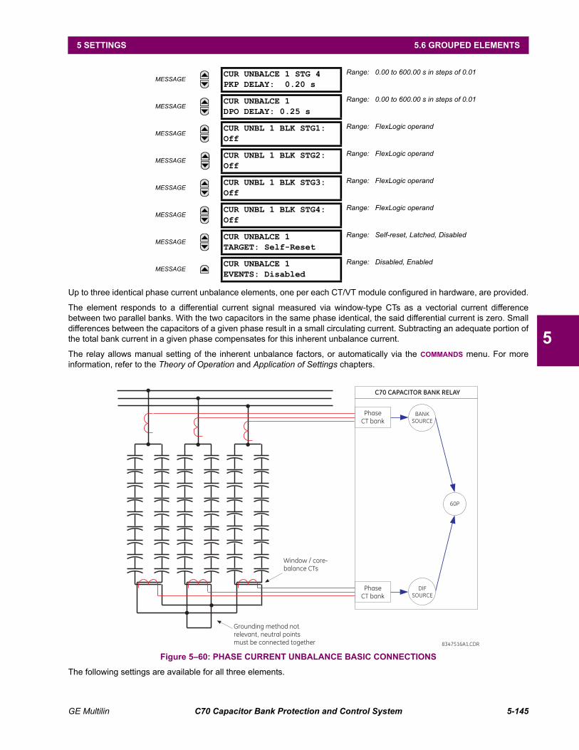
GE Multilin C70 Capacitor Bank Protection and Control System 5-145
5 SETTINGS 5.6 GROUPED ELEMENTS
5
Up to three identical phase current unbalance elements, one per each CT/VT module configured in hardware, are provided.
The element responds to a differential current signal measured via window-type CTs as a vectorial current differencebetween two parallel banks. With the two capacitors in the same phase identical, the said differential current is zero. Smalldifferences between the capacitors of a given phase result in a small circulating current. Subtracting an adequate portion ofthe total bank current in a given phase compensates for this inherent unbalance current.
The relay allows manual setting of the inherent unbalance factors, or automatically via the COMMANDS menu. For moreinformation, refer to the Theory of Operation and Application of Settings chapters.
Figure 5–60: PHASE CURRENT UNBALANCE BASIC CONNECTIONS
The following settings are available for all three elements.
MESSAGECUR UNBALCE 1 STG 4PKP DELAY: 0.20 s
Range: 0.00 to 600.00 s in steps of 0.01
MESSAGECUR UNBALCE 1DPO DELAY: 0.25 s
Range: 0.00 to 600.00 s in steps of 0.01
MESSAGECUR UNBL 1 BLK STG1:Off
Range: FlexLogic operand
MESSAGECUR UNBL 1 BLK STG2:Off
Range: FlexLogic operand
MESSAGECUR UNBL 1 BLK STG3:Off
Range: FlexLogic operand
MESSAGECUR UNBL 1 BLK STG4:Off
Range: FlexLogic operand
MESSAGECUR UNBALCE 1TARGET: Self-Reset
Range: Self-reset, Latched, Disabled
MESSAGECUR UNBALCE 1EVENTS: Disabled
Range: Disabled, Enabled
C70 CAPACITOR BANK RELAY
60P
BANK
SOURCE
Phase
CT bank
Grounding method not
relevant, neutral points
must be connected together
DIF
SOURCE
Window / core-
balance CTs
Phase
CT bank
8347516A1.CDR

5-146 C70 Capacitor Bank Protection and Control System GE Multilin
5.6 GROUPED ELEMENTS 5 SETTINGS
5
• CUR UNBALCE 1 STG 1A PICKUP to CUR UNBALCE 1 STG 4C PICKUP: These settings specify pickup thresholdsfor stages 1 through 4 in phases A through C in per-units (pu) of the nominal current of the differential source. A valueof 1 pu is the nominal secondary current, or the nominal primary current, respectively, as configured under the differen-tial source of this function.
• CUR UNBALCE 1 STG 1 PKP DELAY to CUR UNBALCE 1 STG 4 PKP DELAY: This setting specifies the pickuptime delay, individually per each stage of alarming/tripping. Note that each of the twelve comparators (four stages inthree phases) uses an individual timer, but settings for these timers are controlled individually per each stage, not perphase. The timers use a common drop out time delay specified by the next setting.
• CUR UNBALCE 1 DPO DELAY: This setting controls a drop out delay for the operate FlexLogic operands. Note thatindividual stages apply individually configurable pickup delays, but use this common drop out delay.
• CUR UNBL 1 BLK STG1 to CUR UNBL 1 BLK STG4: These settings are used to block the function on a per-stagebasis when required. At minimum this function shall be blocked when the two banks are not paralleled. Note that whenunblocked, the function becomes operational after five cycles of intentional delay. High-set instantaneous protection onenergization can be provided by a separate instantaneous overcurrent function.
Figure 5–61: PHASE CURRENT UNBALANCE SCHEME LOGIC
IA_op > PICKUP
tPKP
tDPO
tPKP
tDPO
tPKP
tDPO
SETTINGS
CUR UNBALCE 1
BANK SOURCE:
IA
IB
IC
CUR UNBALCE 1 DIF
SOURCE:
IA_dif
IB_dif
IC_dif
SETTINGS
CUR UNBALCE 1
INHNT FACTOR A:
SETTING
CUR UNBALCE 1 STG
1A PICKUP:
SETTING
CUR UNBALCE 1 STG
2A PICKUP:
SETTING
CUR UNBALCE 1 STG
3A PICKUP:
SETTING
CUR UNBALCE 1 STG
4A PICKUP:
CUR BAL 1 STG 1A PKP
FLEXLOGIC OPERAND
CUR BAL 1 STG 2A PKP
FLEXLOGIC OPERAND
CUR BAL 1 STG 3A PKP
FLEXLOGIC OPERAND
CUR BAL 1 STG 4A PKP
FLEXLOGIC OPERAND
tPKP
tDPO
TIMERS
CUR UNBALCE 1 STG
1 PKP DELAY:
CUR UNBALCE 1 STG
2 PKP DELAY:
CUR UNBALCE 1 STG
3 PKP DELAY:
CUR UNBALCE 1 STG
4 PKP DELAY:
CUR BAL 1 STG 1A OP
FLEXLOGIC OPERAND
CUR BAL 1 STG 2A OP
FLEXLOGIC OPERAND
CUR BAL 1 STG 3A OP
FLEXLOGIC OPERAND
CUR BAL 1 STG 4A OP
FLEXLOGIC OPERAND
CUR BAL 1 PKP B
FLEXLOGIC OPERANDS
CUR UNBALCE 1 DPO
DELAY:
CUR BAL 1 PKP A
CUR BAL 1 PKP C
OR
FLEXLOGIC OPERAND
CUR BAL 1 PKPOR
CUR BAL 1 OP B
FLEXLOGIC OPERANDS
CUR BAL 1 OP A
CUR BAL 1 OP C
OR
FLEXLOGIC OPERAND
CUR BAL 1 OPOR
CUR BAL 1 DPO
PHASE C
5 cycles
0
TIMER
RUN 60P FUNCTION
PHASE B
COMMANDS
AUTO-SETTING
PROCEDURE
AN
D
SETTING
COMMANDS/ CUR
UNBALACE 1 AUTO-
SETTING:
Auto
WRITE A NEW SETTING
AN
D
IC_mag > 0.25pu
IB_mag > 0.25pu
IA_mag > 0.25pu
SETTINGS
CUR UNBALCE 1
FUNCTION:
Enabled = 1
CUR UNBL 1 BLK STG1:
Off = 0
CUR UNBL 1 BLK STG2:
Off = 0
CUR UNBL 1 BLK STG3:
Off = 0
CUR UNBL 1 BLK STG4:
Off = 0
AN
D
INHIBIT STAGE 1
INHIBIT STAGE 3
INHIBIT STAGE 4
INHIBIT STAGE 2
Apply?
RUNRUN
IA_op > PICKUP
RUN
IA_op > PICKUP
RUN
IA_op > PICKUP
RUN
AN
DA
ND
AN
DA
ND
Manual
AN
D
834729A2.CDR
PHASE CT "None" = 0
AN
D
AN
D
⎟ ⎠⎞⎜ ⎝⎛
××
−×
=
Ab
an
k
dif
f
ba
nk
AA
dif
f
Ao
p
Inn
kI
I
__
ed
iff_
so
urc
se
co
nd
ary
_
_
ma
g
CT
1

GE Multilin C70 Capacitor Bank Protection and Control System 5-147
5 SETTINGS 5.6 GROUPED ELEMENTS
5
5.6.5 NEUTRAL CURRENT
a) MAIN MENU
PATH: SETTINGS GROUPED ELEMENTS SETTING GROUP 1(6) NEUTRAL CURRENT
The C70 contains protection elements for neutral time overcurrent (ANSI device 51G), neutral instantaneous overcurrent(ANSI device 50G), and neutral current unbalance (ANSI device 60N). A maximum of six ground time overcurrent andtwelve ground instantaneous overcurrent elements are available, dependent on the CT/VT modules ordered with the relay.Three neutral current unbalance elements are available.
NEUTRAL CURRENT
NEUTRAL TOC1
See page 5–148.
MESSAGE NEUTRAL TOC2
See page 5–148.
MESSAGE NEUTRAL TOC6
See page 5–148.
MESSAGE NEUTRAL IOC1
See page 5–149.
MESSAGE NEUTRAL IOC2
See page 5–149.
MESSAGE NEUTRAL IOC12
See page 5–149.
MESSAGE NEUTRAL DIRECTIONAL OC1
See page 5–150.
MESSAGE NEUTRAL CURRENT UNBALANCE 1
See page 5–154.
MESSAGE NEUTRAL CURRENT UNBALANCE 2
See page 5–154.
MESSAGE NEUTRAL CURRENT UNBALANCE 3
See page 5–154.

5-148 C70 Capacitor Bank Protection and Control System GE Multilin
5.6 GROUPED ELEMENTS 5 SETTINGS
5
b) NEUTRAL TIME OVERCURRENT (ANSI 51N, IEC PTOC)
PATH: SETTINGS GROUPED ELEMENTS SETTING GROUP 1(6) NEUTRAL CURRENT NEUTRAL TOC1(6)
The neutral time overcurrent element can provide a desired time-delay operating characteristic versus the applied currentor be used as a simple definite time element. The neutral current input value is a quantity calculated as 3Io from the phasecurrents and may be programmed as fundamental phasor magnitude or total waveform RMS magnitude as required by theapplication.
Two methods of resetting operation are available: “Timed” and “Instantaneous” (refer to the Inverse time overcurrent curvecharacteristics section for details on curve setup, trip times and reset operation). When the element is blocked, the timeaccumulator will reset according to the reset characteristic. For example, if the element reset characteristic is set to “Instan-taneous” and the element is blocked, the time accumulator will be cleared immediately.
Figure 5–62: NEUTRAL TIME OVERCURRENT 1 SCHEME LOGIC
NEUTRAL TOC1
NEUTRAL TOC1FUNCTION: Disabled
Range: Disabled, Enabled
MESSAGENEUTRAL TOC1 SIGNALSOURCE: SRC 1
Range: SRC 1, SRC 2
MESSAGENEUTRAL TOC1INPUT: Phasor
Range: Phasor, RMS
MESSAGENEUTRAL TOC1PICKUP: 1.000 pu
Range: 0.000 to 30.000 pu in steps of 0.001
MESSAGENEUTRAL TOC1CURVE: IEEE Mod Inv
Range: See OVERCURRENT CURVE TYPES table
MESSAGENEUTRAL TOC1TD MULTIPLIER: 1.00
Range: 0.00 to 600.00 in steps of 0.01
MESSAGENEUTRAL TOC1RESET: Instantaneous
Range: Instantaneous, Timed
MESSAGENEUTRAL TOC1 BLOCK:Off
Range: FlexLogic operand
MESSAGENEUTRAL TOC1TARGET: Self-reset
Range: Self-reset, Latched, Disabled
MESSAGENEUTRAL TOC1EVENTS: Disabled
Range: Disabled, Enabled
SETTINGNEUTRAL TOC1FUNCTION:Disabled = 0Enabled = 1
SETTINGNEUTRAL TOC1SOURCE:IN
NEUTRAL TOC1BLOCK:Off = 0
NEUTRAL TOC1CURVE:NEUTRAL TOC1TD MULTIPLIER:NEUTRAL TOC 1RESET:
SETTINGS
SETTING
IN ≥ PICKUP
I
t
NEUTRAL TOC1PICKUP:
RUN
827034A3.VSD
FLEXLOGIC OPERANDS
NEUTRAL TOC1 DPONEUTRAL TOC1 OP
NEUTRAL TOC1INPUT:
ANDNEUTRAL TOC1 PKP

GE Multilin C70 Capacitor Bank Protection and Control System 5-149
5 SETTINGS 5.6 GROUPED ELEMENTS
5
c) NEUTRAL INSTANTANEOUS OVERCURRENT (ANSI 50N, IEC PIOC)
PATH: SETTINGS GROUPED ELEMENTS SETTING GROUP 1(6) NEUTRAL CURRENT NEUTRAL IOC1(12)
The neutral instantaneous overcurrent element may be used as an instantaneous function with no intentional delay or as adefinite time function. The element essentially responds to the magnitude of a neutral current fundamental frequency pha-sor calculated from the phase currents. A positive-sequence restraint is applied for better performance. A small portion(6.25%) of the positive-sequence current magnitude is subtracted from the zero-sequence current magnitude when formingthe operating quantity of the element as follows:
(EQ 5.15)
The positive-sequence restraint allows for more sensitive settings by counterbalancing spurious zero-sequence currentsresulting from:
• System unbalances under heavy load conditions
• Transformation errors of current transformers (CTs) during double-line and three-phase faults.
• Switch-off transients during double-line and three-phase faults.
The positive-sequence restraint must be considered when testing for pickup accuracy and response time (multiple ofpickup). The operating quantity depends on how test currents are injected into the relay (single-phase injection:
; three-phase pure zero-sequence injection: ).
Figure 5–63: NEUTRAL IOC1 SCHEME LOGIC
NEUTRAL IOC1
NEUTRAL IOC1FUNCTION: Disabled
Range: Disabled, Enabled
MESSAGENEUTRAL IOC1 SIGNALSOURCE: SRC 1
Range: SRC 1, SRC 2
MESSAGENEUTRAL IOC1PICKUP: 1.000 pu
Range: 0.000 to 30.000 pu in steps of 0.001
MESSAGENEUTRAL IOC1 PICKUPDELAY: 0.00 s
Range: 0.00 to 600.00 s in steps of 0.01
MESSAGENEUTRAL IOC1 RESETDELAY: 0.00 s
Range: 0.00 to 600.00 s in steps of 0.01
MESSAGENEUTRAL IOC1 BLOCK:Off
Range: FlexLogic operand
MESSAGENEUTRAL IOC1TARGET: Self-reset
Range: Self-reset, Latched, Disabled
MESSAGENEUTRAL IOC1EVENTS: Disabled
Range: Disabled, Enabled
Iop 3 I_0 K I_1– = where K 1 16=
Iop 0.9375 Iinjected= Iop 3 Iinjected=
FLEXLOGIC OPERANDS
NEUTRAL IOC1 FUNCTION:
NEUTRAL IOC1 PICKUP:
NEUTRAL IOC1 SOURCE:
NEUTRAL IOC1 BLOCK:
NEUTRAL IOC1 DPO
NEUTRAL IOC1 OP
NEUTRAL IOC1 PKP
RUNAND
827035A4.CDR
SETTING
SETTINGEnabled=1
Disabled=0
SETTING
SETTING
I_0
Off=0
SETTINGS
NEUTRAL IOC1RESET DELAY :
NEUTRAL IOC1PICKUP DELAY :
tPKP
tRST3( _0 - K _1 ) PICKUPI I

5-150 C70 Capacitor Bank Protection and Control System GE Multilin
5.6 GROUPED ELEMENTS 5 SETTINGS
5
d) NEUTRAL DIRECTIONAL OVERCURRENT (ANSI 67N, IEC PDEF/PTOC)
PATH: SETTINGS GROUPED ELEMENTS SETTING GROUP 1(6) NEUTRAL CURRENT NEUTRAL DIRECTIONAL OC1
The neutral directional overcurrent element provides both forward and reverse fault direction indications the NEUTRAL DIROC1 FWD and NEUTRAL DIR OC1 REV operands, respectively. The output operand is asserted if the magnitude of the oper-ating current is above a pickup level (overcurrent unit) and the fault direction is seen as forward or reverse, respectively(directional unit).
The overcurrent unit responds to the magnitude of a fundamental frequency phasor of the either the neutral current calcu-lated from the phase currents or the ground current. There are separate pickup settings for the forward-looking andreverse-looking functions. If set to use the calculated 3I_0, the element applies a positive-sequence restraint for better per-formance: a small user-programmable portion of the positive-sequence current magnitude is subtracted from the zero-sequence current magnitude when forming the operating quantity.
(EQ 5.16)
The positive-sequence restraint allows for more sensitive settings by counterbalancing spurious zero-sequence currentsresulting from:
• System unbalances under heavy load conditions.
NEUTRAL DIRECTIONAL OC1
NEUTRAL DIR OC1FUNCTION: Disabled
Range: Disabled, Enabled
MESSAGENEUTRAL DIR OC1SOURCE: SRC 1
Range: SRC 1, SRC 2
MESSAGENEUTRAL DIR OC1POLARIZING: Voltage
Range: Voltage, Current, Dual
MESSAGENEUTRAL DIR OC1 POLVOLT: Calculated V0
Range: Calculated V0, Measured VX
MESSAGENEUTRAL DIR OC1 OPCURR: Calculated 3I0
Range: Calculated 3I0, Measured IG
MESSAGENEUTRAL DIR OC1 POS-SEQ RESTRAINT: 0.063
Range: 0.000 to 0.500 in steps of 0.001
MESSAGENEUTRAL DIR OC1OFFSET: 0.00
Range: 0.00 to 250.00 in steps of 0.01
MESSAGENEUTRAL DIR OC1 FWDECA: 75° Lag
Range: –90 to 90° in steps of 1
MESSAGENEUTRAL DIR OC1 FWDLIMIT ANGLE: 90°
Range: 40 to 90° in steps of 1
MESSAGENEUTRAL DIR OC1 FWDPICKUP: 0.050 pu
Range: 0.006 to 30.000 pu in steps of 0.001
MESSAGENEUTRAL DIR OC1 REVLIMIT ANGLE: 90°
Range: 40 to 90° in steps of 1
MESSAGENEUTRAL DIR OC1 REVPICKUP: 0.050 pu
Range: 0.006 to 30.000 pu in steps of 0.001
MESSAGENEUTRAL DIR OC1 BLK:Off
Range: FlexLogic operand
MESSAGENEUTRAL DIR OC1TARGET: Self-reset
Range: Self-reset, Latched, Disabled
MESSAGENEUTRAL DIR OC1EVENTS: Disabled
Range: Disabled, Enabled
Iop 3 I_0 K I_1– =

GE Multilin C70 Capacitor Bank Protection and Control System 5-151
5 SETTINGS 5.6 GROUPED ELEMENTS
5
• Transformation errors of current transformers (CTs) during double-line and three-phase faults.
• Switch-off transients during double-line and three-phase faults.
The positive-sequence restraint must be considered when testing for pickup accuracy and response time (multiple ofpickup). The operating quantity depends on the way the test currents are injected into the relay (single-phase injection:Iop = (1 – K) Iinjected ; three-phase pure zero-sequence injection: Iop = 3 Iinjected).
The positive-sequence restraint is removed for low currents. If the positive-sequence current is below 0.8 pu, the restraint isremoved by changing the constant K to zero. This facilitates better response to high-resistance faults when the unbalanceis very small and there is no danger of excessive CT errors as the current is low.
The directional unit uses the zero-sequence current (I_0) or ground current (IG) for fault direction discrimination and maybe programmed to use either zero-sequence voltage (“Calculated V0” or “Measured VX”), ground current (IG), or both forpolarizing. The zero-sequence current (I_0) must be greater than the PRODUCT SETUP DISPLAY PROPERTIES CUR-
RENT CUT-OFF LEVEL setting value and IG must be greater than 0.5 pu to be validated as the operating quantity for direc-tional current. The following tables define the neutral directional overcurrent element.
where: ,
,
ECA = element characteristic angle and IG = ground current
When NEUTRAL DIR OC1 POL VOLT is set to “Measured VX”, one-third of this voltage is used in place of V_0. The followingfigure explains the usage of the voltage polarized directional unit of the element.
The figure below shows the voltage-polarized phase angle comparator characteristics for a phase A to ground fault, with:
• ECA = 90° (element characteristic angle = centerline of operating characteristic)
• FWD LA = 80° (forward limit angle = the ± angular limit with the ECA for operation)
• REV LA = 80° (reverse limit angle = the ± angular limit with the ECA for operation)
The above bias should be taken into account when using the neutral directional overcurrent element to directionalize otherprotection elements.
Table 5–20: QUANTITIES FOR "CALCULATED 3I0" CONFIGURATION
DIRECTIONAL UNITOVERCURRENT UNIT
POLARIZING MODE DIRECTION COMPARED PHASORS
VoltageForward –V_0 + Z_offset I_0 I_0 1ECA
Iop = 3 (|I_0| – K |I_1|) if |I1| > 0.8 pu
Iop = 3 (|I_0|) if |I1| 0.8 pu
Reverse –V_0 + Z_offset I_0 –I_0 1ECA
CurrentForward IG I_0
Reverse IG –I_0
Dual
Forward
–V_0 + Z_offset I_0 I_0 1ECAor
IG I_0
Reverse
–V_0 + Z_offset I_0 –I_0 1ECAor
IG –I_0
Table 5–21: QUANTITIES FOR "MEASURED IG" CONFIGURATION
DIRECTIONAL UNITOVERCURRENT UNIT
POLARIZING MODE DIRECTION COMPARED PHASORS
VoltageForward –V_0 + Z_offset IG/3 IG 1ECA
Iop = |IG|Reverse –V_0 + Z_offset IG/3 –IG 1ECA
V_013--- VAG VBG VCG+ + zero sequence voltage= =
I_013---IN
13--- IA IB IC+ + zero sequence current= = =

5-152 C70 Capacitor Bank Protection and Control System GE Multilin
5.6 GROUPED ELEMENTS 5 SETTINGS
5 Figure 5–64: NEUTRAL DIRECTIONAL VOLTAGE-POLARIZED CHARACTERISTICS
• NEUTRAL DIR OC1 POLARIZING: This setting selects the polarizing mode for the directional unit.
– If “Voltage” polarizing is selected, the element uses the zero-sequence voltage angle for polarization. The usercan use either the zero-sequence voltage V_0 calculated from the phase voltages, or the zero-sequence voltagesupplied externally as the auxiliary voltage V_X, both from the NEUTRAL DIR OC1 SOURCE.
The calculated V_0 can be used as polarizing voltage only if the voltage transformers are connected in Wye. Theauxiliary voltage can be used as the polarizing voltage provided SYSTEM SETUP AC INPUTS VOLTAGE BANK
AUXILIARY VT CONNECTION is set to “Vn” and the auxiliary voltage is connected to a zero-sequence voltagesource (such as broken delta connected secondary of VTs).
The zero-sequence (V_0) or auxiliary voltage (V_X), accordingly, must be greater than 0.02 pu to be validated foruse as a polarizing signal. If the polarizing signal is invalid, neither forward nor reverse indication is given.
– If “Current” polarizing is selected, the element uses the ground current angle connected externally and configuredunder NEUTRAL OC1 SOURCE for polarization. The ground CT must be connected between the ground and neutralpoint of an adequate local source of ground current. The ground current must be greater than 0.05 pu to be vali-dated as a polarizing signal. If the polarizing signal is not valid, neither forward nor reverse indication is given. Inaddition, the zero-sequence current (I_0) must be greater than the PRODUCT SETUP DISPLAY PROPERTIES CURRENT CUT-OFF LEVEL setting value.
For a choice of current polarizing, it is recommended that the polarizing signal be analyzed to ensure that a knowndirection is maintained irrespective of the fault location. For example, if using an autotransformer neutral currentas a polarizing source, it should be ensured that a reversal of the ground current does not occur for a high-sidefault. The low-side system impedance should be assumed minimal when checking for this condition. A similar sit-uation arises for a wye/delta/wye transformer, where current in one transformer winding neutral may reverse whenfaults on both sides of the transformer are considered.
– If “Dual” polarizing is selected, the element performs both directional comparisons as described above. A givendirection is confirmed if either voltage or current comparators indicate so. If a conflicting (simultaneous forwardand reverse) indication occurs, the forward direction overrides the reverse direction.
• NEUTRAL DIR OC1 POL VOLT: Selects the polarizing voltage used by the directional unit when "Voltage" or "Dual"polarizing mode is set. The polarizing voltage can be programmed to be either the zero-sequence voltage calculatedfrom the phase voltages ("Calculated V0") or supplied externally as an auxiliary voltage ("Measured VX").
827805A1.CDR
VAG(reference)
VBG
VCG
–3I_0 line
3I_0 line
ECA line
–ECA line
LA
LA
LA
LA
ECA
FWD LAline
FWD OperatingRegion
REV OperatingRegion
FWD LAline
REV LAline
REV LAline
–3V_0 line
3V_0 line

GE Multilin C70 Capacitor Bank Protection and Control System 5-153
5 SETTINGS 5.6 GROUPED ELEMENTS
5
• NEUTRAL DIR OC1 OP CURR: This setting indicates whether the 3I_0 current calculated from the phase currents, orthe ground current shall be used by this protection. This setting acts as a switch between the neutral and groundmodes of operation (67N and 67G). If set to “Calculated 3I0” the element uses the phase currents and applies the pos-itive-sequence restraint; if set to “Measured IG” the element uses ground current supplied to the ground CT of the CTbank configured as NEUTRAL DIR OC1 SOURCE. If this setting is “Measured IG”, then the NEUTRAL DIR OC1 POLARIZING
setting must be “Voltage”, as it is not possible to use the ground current as an operating and polarizing signal simulta-neously. IG current has to be above 0.05 ps to be used as operate quantity.
• NEUTRAL DIR OC1 POS-SEQ RESTRAINT: This setting controls the amount of the positive-sequence restraint. Setto 0.063 for backward compatibility with firmware revision 3.40 and older. Set to zero to remove the restraint. Sethigher if large system unbalances or poor CT performance are expected.
• NEUTRAL DIR OC1 OFFSET: This setting specifies the offset impedance used by this protection. The primary appli-cation for the offset impedance is to guarantee correct identification of fault direction on series compensated lines. Inregular applications, the offset impedance ensures proper operation even if the zero-sequence voltage at the relayingpoint is very small. If this is the intent, the offset impedance shall not be larger than the zero-sequence impedance ofthe protected circuit. Practically, it shall be several times smaller. The offset impedance shall be entered in secondaryohms.
• NEUTRAL DIR OC1 FWD ECA: This setting defines the characteristic angle (ECA) for the forward direction in the"Voltage" polarizing mode. The "Current" polarizing mode uses a fixed ECA of 0°. The ECA in the reverse direction isthe angle set for the forward direction shifted by 180°.
• NEUTRAL DIR OC1 FWD LIMIT ANGLE: This setting defines a symmetrical (in both directions from the ECA) limitangle for the forward direction.
• NEUTRAL DIR OC1 FWD PICKUP: This setting defines the pickup level for the overcurrent unit of the element in theforward direction. When selecting this setting it must be kept in mind that the design uses a ‘positive-sequencerestraint’ technique for the “Calculated 3I0” mode of operation.
• NEUTRAL DIR OC1 REV LIMIT ANGLE: This setting defines a symmetrical (in both directions from the ECA) limitangle for the reverse direction.
• NEUTRAL DIR OC1 REV PICKUP: This setting defines the pickup level for the overcurrent unit of the element in thereverse direction. When selecting this setting it must be kept in mind that the design uses a positive-sequence restrainttechnique for the “Calculated 3I0” mode of operation.
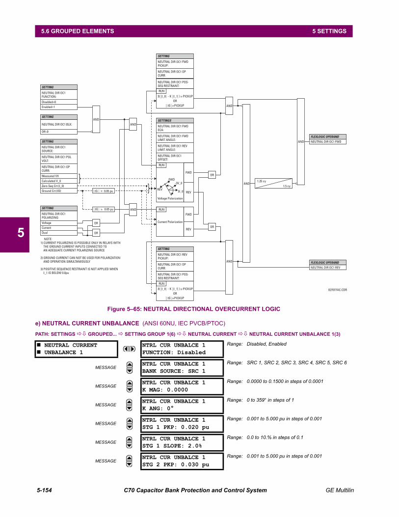
5-154 C70 Capacitor Bank Protection and Control System GE Multilin
5.6 GROUPED ELEMENTS 5 SETTINGS
5
Figure 5–65: NEUTRAL DIRECTIONAL OVERCURRENT LOGIC
e) NEUTRAL CURRENT UNBALANCE (ANSI 60NU, IEC PVCB/PTOC)
PATH: SETTINGS GROUPED... SETTING GROUP 1(6) NEUTRAL CURRENT NEUTRAL CURRENT UNBALANCE 1(3)
NEUTRAL CURRENT UNBALANCE 1
NTRL CUR UNBALCE 1FUNCTION: Disabled
Range: Disabled, Enabled
MESSAGENTRL CUR UNBALCE 1BANK SOURCE: SRC 1
Range: SRC 1, SRC 2, SRC 3, SRC 4, SRC 5, SRC 6
MESSAGENTRL CUR UNBALCE 1K MAG: 0.0000
Range: 0.0000 to 0.1500 in steps of 0.0001
MESSAGENTRL CUR UNBALCE 1K ANG: 0°
Range: 0 to 359° in steps of 1
MESSAGENTRL CUR UNBALCE 1STG 1 PKP: 0.020 pu
Range: 0.001 to 5.000 pu in steps of 0.001
MESSAGENTRL CUR UNBALCE 1STG 1 SLOPE: 2.0%
Range: 0.0 to 10.% in steps of 0.1
MESSAGENTRL CUR UNBALCE 1STG 2 PKP: 0.030 pu
Range: 0.001 to 5.000 pu in steps of 0.001

GE Multilin C70 Capacitor Bank Protection and Control System 5-155
5 SETTINGS 5.6 GROUPED ELEMENTS
5
Up to three identical neutral current unbalance elements, one per each installed CT/VT module.
The neutral current unbalance element responds to a differential current signal measured as a vectorial current differencebetween neutral currents of parallel banks. In case of ungrounded banks, regular, preferably low-ratio CT can be used. Incase of grounded banks, a window or core-balance CT shall be used for increased accuracy/sensitivity.
The function applies simplified compensation for the inherent bank unbalance. Accurate compensation requires three bal-ancing factors that are difficult to measure in practical situations. Instead, a simple and practical compensation respondingto both the positive-sequence current and negative-sequence current is applied. This method is easy to apply and remainsaccurate as long as the zero-sequence bank currents are relatively small. Under large zero-sequence bank currents, theapplied method of compensation for the inherent bank unbalance is less accurate. The solution to this problem is to use asmall portion of the zero-sequence current at the bank terminals to produce extra restraint and preserve high sensitivity ofthis protection method.
By setting both the slope and the inherent unbalance compensating factor to zero one could apply the function as a plainovercurrent element responding to the split-phase neutral current.
MESSAGENTRL CUR UNBALCE 1STG 2 SLOPE: 2.0%
Range: 0.0 to 10.% in steps of 0.1
MESSAGENTRL CUR UNBALCE 1STG 3 PKP: 0.040 pu
Range: 0.001 to 5.000 pu in steps of 0.001
MESSAGENTRL CUR UNBALCE 1STG 3 SLOPE: 2.0%
Range: 0.0 to 10.% in steps of 0.1
MESSAGENTRL CUR UNBALCE 1STG 4 PKP: 0.050 pu
Range: 0.001 to 5.000 pu in steps of 0.001
MESSAGENTRL CUR UNBALCE 1STG 4 SLOPE: 5.0%
Range: 0.0 to 10.% in steps of 0.1
MESSAGENTRL CUR UNBALCE 1STG 1 DEL: 30.00 s
Range: 0.00 to 600.00 s in steps of 0.01
MESSAGENTRL CUR UNBALCE 1STG 2 DEL: 10.00 s
Range: 0.00 to 600.00 s in steps of 0.01
MESSAGENTRL CUR UNBALCE 1STG 3 DEL: 1.00 s
Range: 0.00 to 600.00 s in steps of 0.01
MESSAGENTRL CUR UNBALCE 1STG 4 DEL: 0.20 s
Range: 0.00 to 600.00 s in steps of 0.01
MESSAGENTRL CUR UNBALCE 1DPO DELAY: 0.25 s
Range: 0.00 to 600.00 s in steps of 0.01
MESSAGENTRL CUR 1 BLK STG1:Off
Range: FlexLogic operand
MESSAGENTRL CUR 1 BLK STG2:Off
Range: FlexLogic operand
MESSAGENTRL CUR 1 BLK STG3:Off
Range: FlexLogic operand
MESSAGENTRL CUR 1 BLK STG4:Off
Range: FlexLogic operand
MESSAGENTRL CUR UNBALCE 1TARGET: Self-Reset
Range: Self-reset, Latched, Disabled
MESSAGENTRL CUR UNBALCE 1EVENTS: Disabled
Range: Disabled, Enabled
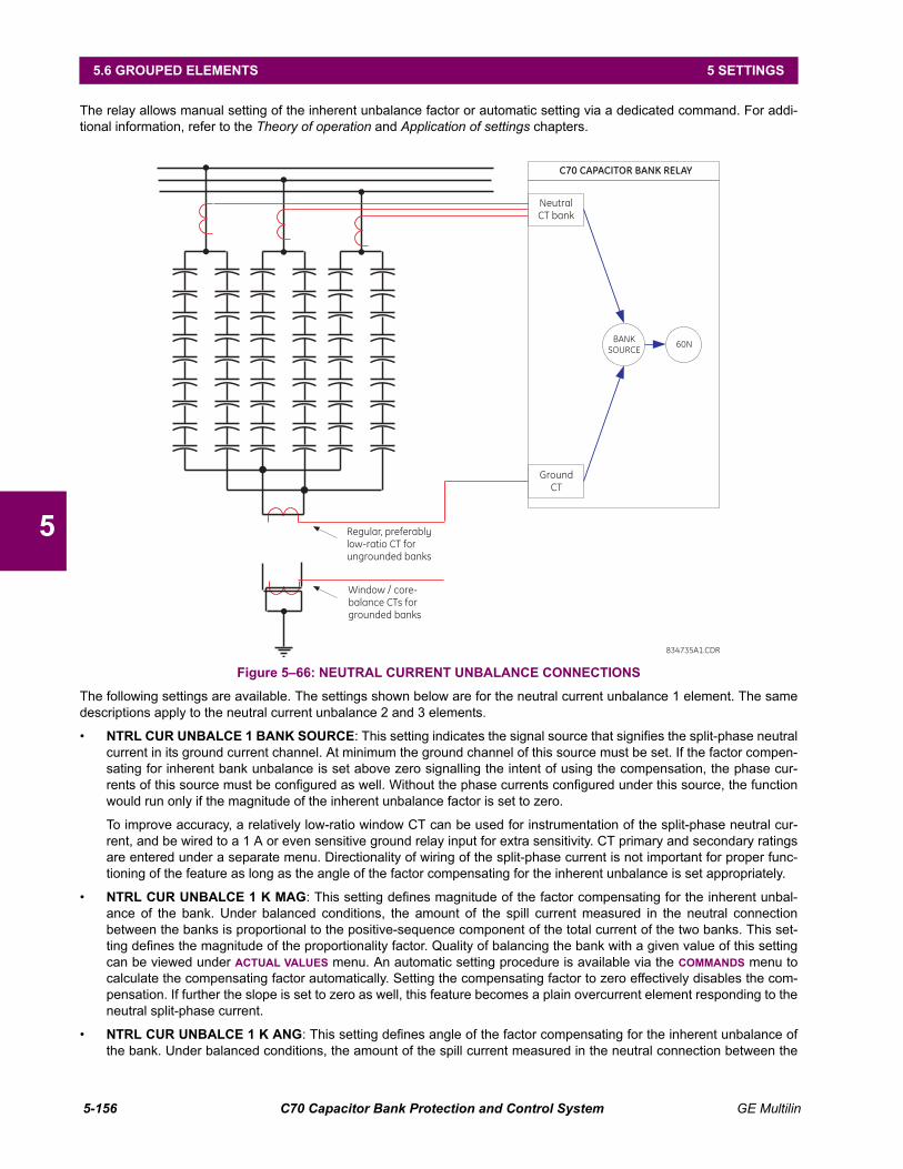
5-156 C70 Capacitor Bank Protection and Control System GE Multilin
5.6 GROUPED ELEMENTS 5 SETTINGS
5
The relay allows manual setting of the inherent unbalance factor or automatic setting via a dedicated command. For addi-tional information, refer to the Theory of operation and Application of settings chapters.
Figure 5–66: NEUTRAL CURRENT UNBALANCE CONNECTIONS
The following settings are available. The settings shown below are for the neutral current unbalance 1 element. The samedescriptions apply to the neutral current unbalance 2 and 3 elements.
• NTRL CUR UNBALCE 1 BANK SOURCE: This setting indicates the signal source that signifies the split-phase neutralcurrent in its ground current channel. At minimum the ground channel of this source must be set. If the factor compen-sating for inherent bank unbalance is set above zero signalling the intent of using the compensation, the phase cur-rents of this source must be configured as well. Without the phase currents configured under this source, the functionwould run only if the magnitude of the inherent unbalance factor is set to zero.
To improve accuracy, a relatively low-ratio window CT can be used for instrumentation of the split-phase neutral cur-rent, and be wired to a 1 A or even sensitive ground relay input for extra sensitivity. CT primary and secondary ratingsare entered under a separate menu. Directionality of wiring of the split-phase current is not important for proper func-tioning of the feature as long as the angle of the factor compensating for the inherent unbalance is set appropriately.
• NTRL CUR UNBALCE 1 K MAG: This setting defines magnitude of the factor compensating for the inherent unbal-ance of the bank. Under balanced conditions, the amount of the spill current measured in the neutral connectionbetween the banks is proportional to the positive-sequence component of the total current of the two banks. This set-ting defines the magnitude of the proportionality factor. Quality of balancing the bank with a given value of this settingcan be viewed under ACTUAL VALUES menu. An automatic setting procedure is available via the COMMANDS menu tocalculate the compensating factor automatically. Setting the compensating factor to zero effectively disables the com-pensation. If further the slope is set to zero as well, this feature becomes a plain overcurrent element responding to theneutral split-phase current.
• NTRL CUR UNBALCE 1 K ANG: This setting defines angle of the factor compensating for the inherent unbalance ofthe bank. Under balanced conditions, the amount of the spill current measured in the neutral connection between the
C70 CAPACITOR BANK RELAY
60NBANK
SOURCE
Neutral
CT bank
Ground
CT
Regular, preferably
low-ratio CT for
ungrounded banks
Window / core-
balance CTs for
grounded banks
834735A1.CDR

GE Multilin C70 Capacitor Bank Protection and Control System 5-157
5 SETTINGS 5.6 GROUPED ELEMENTS
5
banks is proportional to the positive-sequence component of the total current of the two banks. This setting defines theangle of the proportionality factor. Quality of balancing the bank with a given value of this setting can be viewed underACTUAL VALUES menu. An automatic setting procedure is available under the COMMANDS menu to calculate the com-pensating factor automatically. Refer to the Theory of operation chapter for more information regarding the meaning ofthe inherent unbalance compensating factor of this protection method.
• NTRL CUR UNBALCE 1 STG1 PKP to NTRL CUR UNBALCE 1 STG4 PKP: These settings specify pickup thresh-olds for stages 1 through 4 in per-units (pu) of the nominal current of the ground current channel of the bank source. Avalue of 1 pu is the nominal secondary current, or the nominal primary current, respectively, as configured under thebank source of this function.
• NTRL CUR UNBALCE 1 STG1 SLOPE to NTRL CUR UNBALCE 1 STG4 SLOPE: These settings specify the slopesfor stages 1 through 4. The slope setting is applied if the phase CTs are configured under the bank source. The magni-tude of the zero-sequence current is applied as a restraining signal. Typically few percent of slope is enough to ensuresecurity of the function. The factor compensating for the inherent bank unbalance zeroes out the operating signalunder relatively balanced bank currents. If the said currents contain a significant zero sequence component, the qualityof compensation is lower, hence the need for the restraint, and this slope setting. Refer to the Theory of operationchapter for more information on this protection method.
• NTRL CUR UNBALCE 1 STG1 DEL to NTRL CUR UNBALCE 1 STG4 DEL: This setting specifies the pickup timedelay, individually per each stage of alarming/tripping. The timers use a common drop out time delay specified by thenext setting.
• NTRL CUR UNBALCE 1 DPO DELAY: This setting controls a drop out delay for the operate FlexLogic operands. Notethat individual stages apply individually configurable pickup delays, but use this common drop out delay.
• NTRL CUR 1 BLK STG1 to NTRL CUR 1 BLK STG4: These settings are used to block the function on a per stagebasis when required. At minimum this function shall be blocked when the two banks are not paralleled. Note that whenunblocked, the function becomes operational after five cycles of intentional delay. High-set instantaneous protection onenergization can be provided by a separate instantaneous overcurrent function.

5-158 C70 Capacitor Bank Protection and Control System GE Multilin
5.6 GROUPED ELEMENTS 5 SETTINGS
5
Figure 5–67: NEUTRAL CURRENT UNBALANCE SCHEME LOGIC

GE Multilin C70 Capacitor Bank Protection and Control System 5-159
5 SETTINGS 5.6 GROUPED ELEMENTS
5
5.6.6 GROUND CURRENT
a) MAIN MENU
PATH: SETTINGS GROUPED ELEMENTS SETTING GROUP 1(6) GROUND CURRENT
The C70 contains protection elements for ground time overcurrent (ANSI device 51G) and ground instantaneous overcur-rent (ANSI device 50G). A maximum of six ground time overcurrent and eight ground instantaneous overcurrent elementsare available, dependent on the CT/VT modules ordered with the relay. See the following table for details.
GROUND CURRENT
GROUND TOC1
See page 5–160.
MESSAGE GROUND TOC2
See page 5–160.
MESSAGE GROUND TOC6
See page 5–160.
MESSAGE GROUND IOC1
See page 5–161.
MESSAGE GROUND IOC2
See page 5–161.
MESSAGE GROUND IOC12
See page 5–161.
CT/VT MODULES GROUND CURRENT ELEMENTS
SLOT F SLOT M TIME OVERCURRENT
INSTANTANEOUS OVERCURRENT
8F/8G 8F/8G 4 4
8H/8J 6 6
8H/8J 8F/8G 6 6
8H/8J 6 8

5-160 C70 Capacitor Bank Protection and Control System GE Multilin
5.6 GROUPED ELEMENTS 5 SETTINGS
5
b) GROUND TIME OVERCURRENT (ANSI 51G, IEC PTOC)
PATH: SETTINGS GROUPED ELEMENTS SETTING GROUP 1(6) GROUND CURRENT GROUND TOC1(6)
This element can provide a desired time-delay operating characteristic versus the applied current or be used as a simpledefinite time element. The ground current input value is the quantity measured by the ground input CT and is the funda-mental phasor or RMS magnitude. Two methods of resetting operation are available: “Timed” and “Instantaneous” (refer tothe Inverse time overcurrent curve characteristics section for details). When the element is blocked, the time accumulatorwill reset according to the reset characteristic. For example, if the element reset characteristic is set to “Instantaneous” andthe element is blocked, the time accumulator will be cleared immediately.
These elements measure the current that is connected to the ground channel of a CT/VT module. The conversionrange of a standard channel is from 0.02 to 46 times the CT rating.
Figure 5–68: GROUND TOC1 SCHEME LOGIC
GROUND TOC1
GROUND TOC1FUNCTION: Disabled
Range: Disabled, Enabled
MESSAGEGROUND TOC1 SIGNALSOURCE: SRC 1
Range: SRC 1, SRC 2
MESSAGEGROUND TOC1INPUT: Phasor
Range: Phasor, RMS
MESSAGEGROUND TOC1PICKUP: 1.000 pu
Range: 0.000 to 30.000 pu in steps of 0.001
MESSAGEGROUND TOC1CURVE: IEEE Mod Inv
Range: see the Overcurrent Curve Types table
MESSAGEGROUND TOC1TD MULTIPLIER: 1.00
Range: 0.00 to 600.00 in steps of 0.01
MESSAGEGROUND TOC1RESET: Instantaneous
Range: Instantaneous, Timed
MESSAGEGROUND TOC1 BLOCK:Off
Range: FlexLogic operand
MESSAGEGROUND TOC1TARGET: Self-reset
Range: Self-reset, Latched, Disabled
MESSAGEGROUND TOC1EVENTS: Disabled
Range: Disabled, Enabled
NOTE
SETTING
GROUND TOC1
FUNCTION:
Disabled = 0
Enabled = 1
SETTING
GROUND TOC1
SOURCE:
IG
GROUND TOC1
BLOCK:
Off = 0
FLEXLOGIC OPERANDS
GROUND TOC1 DPO
GROUND TOC1 OP
GROUND TOC1
CURVE:
GROUND TOC1
TD MULTIPLIER:
GROUND TOC 1
RESET:
SETTINGS
SETTING
IG ≥ PICKUP
I
t
GROUND TOC1
PICKUP:
RUN
827036A3.VSD
GROUND TOC1
INPUT:
AND
GROUND TOC1 PKP

GE Multilin C70 Capacitor Bank Protection and Control System 5-161
5 SETTINGS 5.6 GROUPED ELEMENTS
5
c) GROUND INSTANTANEOUS OVERCURRENT (ANSI 50G, IEC PIOC)
PATH: SETTINGS GROUPED ELEMENTS SETTING GROUP 1(6) GROUND CURRENT GROUND IOC1(12)
The ground instantaneous overcurrent element may be used as an instantaneous element with no intentional delay or as adefinite time element. The ground current input is the quantity measured by the ground input CT and is the fundamentalphasor magnitude.
These elements measure the current that is connected to the ground channel of a CT/VT module. The conversionrange of a standard channel is from 0.02 to 46 times the CT rating.
Figure 5–69: GROUND IOC1 SCHEME LOGIC
5.6.7 NEGATIVE SEQUENCE CURRENT
a) MAIN MENU
PATH: SETTINGS GROUPED ELEMENTS SETTING GROUP 1(6) NEGATIVE SEQUENCE CURRENT
The C70 relay provides two (2) negative-sequence directional overcurrent elements..
GROUND IOC1
GROUND IOC1FUNCTION: Disabled
Range: Disabled, Enabled
MESSAGEGROUND IOC1 SIGNALSOURCE: SRC 1
Range: SRC 1, SRC 2
MESSAGEGROUND IOC1PICKUP: 1.000 pu
Range: 0.000 to 30.000 pu in steps of 0.001
MESSAGEGROUND IOC1 PICKUPDELAY: 0.00 s
Range: 0.00 to 600.00 s in steps of 0.01
MESSAGEGROUND IOC1 RESETDELAY: 0.00 s
Range: 0.00 to 600.00 s in steps of 0.01
MESSAGEGROUND IOC1 BLOCK:Off
Range: FlexLogic operand
MESSAGEGROUND IOC1TARGET: Self-reset
Range: Self-reset, Latched, Disabled
MESSAGEGROUND IOC1EVENTS: Disabled
Range: Disabled, Enabled
NEGATIVE SEQUENCE CURRENT
NEG SEQ DIR OC1
See page 5–162.
MESSAGE NEG SEQ DIR OC2
See page 5–162.
NOTE
SETTING
GROUND IOC1
FUNCTION:
Disabled = 0
Enabled = 1
SETTING
GROUND IOC1
SOURCE:
IG
GROUND IOC1
BLOCK:
Off = 0
FLEXLOGIC OPERANDS
GROUND IOIC DPO
GROUND IOC1 OP
SETTING
SETTING
IG ≥ PICKUP
GROUND IOC1
PICKUP:
RUN
GROUND IOC1 PICKUP
DELAY:
SETTINGS
GROUND IOC1 RESET
DELAY:
tPKP
tRST
827037A4.VSD
AND
GROUND IOC1 PKP

5-162 C70 Capacitor Bank Protection and Control System GE Multilin
5.6 GROUPED ELEMENTS 5 SETTINGS
5
b) NEGATIVE SEQUENCE DIRECTIONAL OVERCURRENT (ANSI 67Q, IEC PDEF/PTOC)
PATH: SETTINGS GROUPED ELEMENTS SETTING GROUP 1(6) NEGATIVE SEQUENCE CURRENT NEG SEQ DIR OC1
There are two negative-sequence directional overcurrent protection elements available. The element provides both forwardand reverse fault direction indications through its output operands NEG SEQ DIR OC1 FWD and NEG SEQ DIR OC1 REV,respectively. The output operand is asserted if the magnitude of the operating current is above a pickup level (overcurrentunit) and the fault direction is seen as forward or reverse, respectively (directional unit).
The overcurrent unit of the element essentially responds to the magnitude of a fundamental frequency phasor of eitherthe negative-sequence or zero-sequence current as per user selection. The zero-sequence current should not be mistakenwith the neutral current (factor 3 difference).
A positive-sequence restraint is applied for better performance: a small user-programmable portion of the positive-sequence current magnitude is subtracted from the negative or zero-sequence current magnitude, respectively, when form-ing the element operating quantity.
(EQ 5.17)
The positive-sequence restraint allows for more sensitive settings by counterbalancing spurious negative-sequence andzero-sequence currents resulting from:
• System unbalances under heavy load conditions.
• Transformation errors of current transformers (CTs).
• Fault inception and switch-off transients.
NEG SEQ DIR OC1
NEG SEQ DIR OC1FUNCTION: Disabled
Range: Disabled, Enabled
MESSAGENEG SEQ DIR OC1SOURCE: SRC 1
Range: SRC 1, SRC 2
MESSAGENEG SEQ DIR OC1OFFSET: 0.00
Range: 0.00 to 250.00 ohms in steps of 0.01
MESSAGENEG SEQ DIR OC1TYPE: Neg Sequence
Range: Neg Sequence, Zero Sequence
MESSAGENEG SEQ DIR OC1 POS-SEQ RESTRAINT: 0.063
Range: 0.000 to 0.500 in steps of 0.001
MESSAGENEG SEQ DIR OC1 FWDECA: 75° Lag
Range: 0 to 90° Lag in steps of 1
MESSAGENEG SEQ DIR OC1 FWDLIMIT ANGLE: 90°
Range: 40 to 90° in steps of 1
MESSAGENEG SEQ DIR OC1 FWDPICKUP: 0.050 pu
Range: 0.015 to 30.000 pu in steps of 0.001
MESSAGENEG SEQ DIR OC1 REVLIMIT ANGLE: 90°
Range: 40 to 90° in steps of 1
MESSAGENEG SEQ DIR OC1 REVPICKUP: 0.050 pu
Range: 0.015 to 30.000 pu in steps of 0.001
MESSAGENEG SEQ DIR OC1 BLK:Off
Range: FlexLogic operand
MESSAGENEG SEQ DIR OC1TARGET: Self-reset
Range: Self-reset, Latched, Disabled
MESSAGENEG SEQ DIR OC1EVENTS: Disabled
Range: Disabled, Enabled
Iop I_2 K I_1–= or Iop 3 I_0 K I_1– =

GE Multilin C70 Capacitor Bank Protection and Control System 5-163
5 SETTINGS 5.6 GROUPED ELEMENTS
5
The positive-sequence restraint must be considered when testing for pick-up accuracy and response time (multiple ofpickup). The positive-sequence restraint is removed for low currents. If the positive-sequence current is less than 0.8 pu,then the restraint is removed by changing the constant K to zero. This results in better response to high-resistance faultswhen the unbalance is very small and there is no danger of excessive CT errors, since the current is low.
The operating quantity depends on the way the test currents are injected into the C70. For single phase injection:
• Iop = ⅓ (1 – K Iinjected for I_2 mode.
• Iop = (1 – K Iinjected for I_0 mode if I_1 > 0.8 pu.
The directional unit uses the negative-sequence current (I_2) and negative-sequence voltage (V_2).
The following tables define the negative-sequence directional overcurrent element.
Table 5–22: NEGATIVE-SEQUENCE DIRECTIONAL OVERCURRENT UNIT
Table 5–23: NEGATIVE-SEQUENCE DIRECTIONAL UNIT
The negative-sequence voltage must be greater than 0.02 pu to be validated for use as a polarizing signal. If the polarizingsignal is not validated neither forward nor reverse indication is given. The following figure explains the usage of the voltagepolarized directional unit of the element.
The figure below shows the phase angle comparator characteristics for a phase A to ground fault, with settings of:
ECA = 75° (element characteristic angle = centerline of operating characteristic)FWD LA = 80° (forward limit angle = ± the angular limit with the ECA for operation)REV LA = 80° (reverse limit angle = ± the angular limit with the ECA for operation)
MODE OPERATING CURRENT
Negative-sequence Iop = |I_2| – K I_1|
Zero-sequence Iop = 3 × (|I_0| – K × |I_1|) if |I_1| > 0.8 puIop = 3 × |I_0| if |I_1| ≤ 0.8 pu
DIRECTION COMPARED PHASORS
Forward –V_2 Z_offset I_2 I_2 1ECA
Reverse –V_2 Z_offset I_2 –(I_2 1ECA)
Forward –V_2 Z_offset I_2 I_2 1ECA
Reverse –V_2 Z_offset I_2 –(I_2 1ECA)
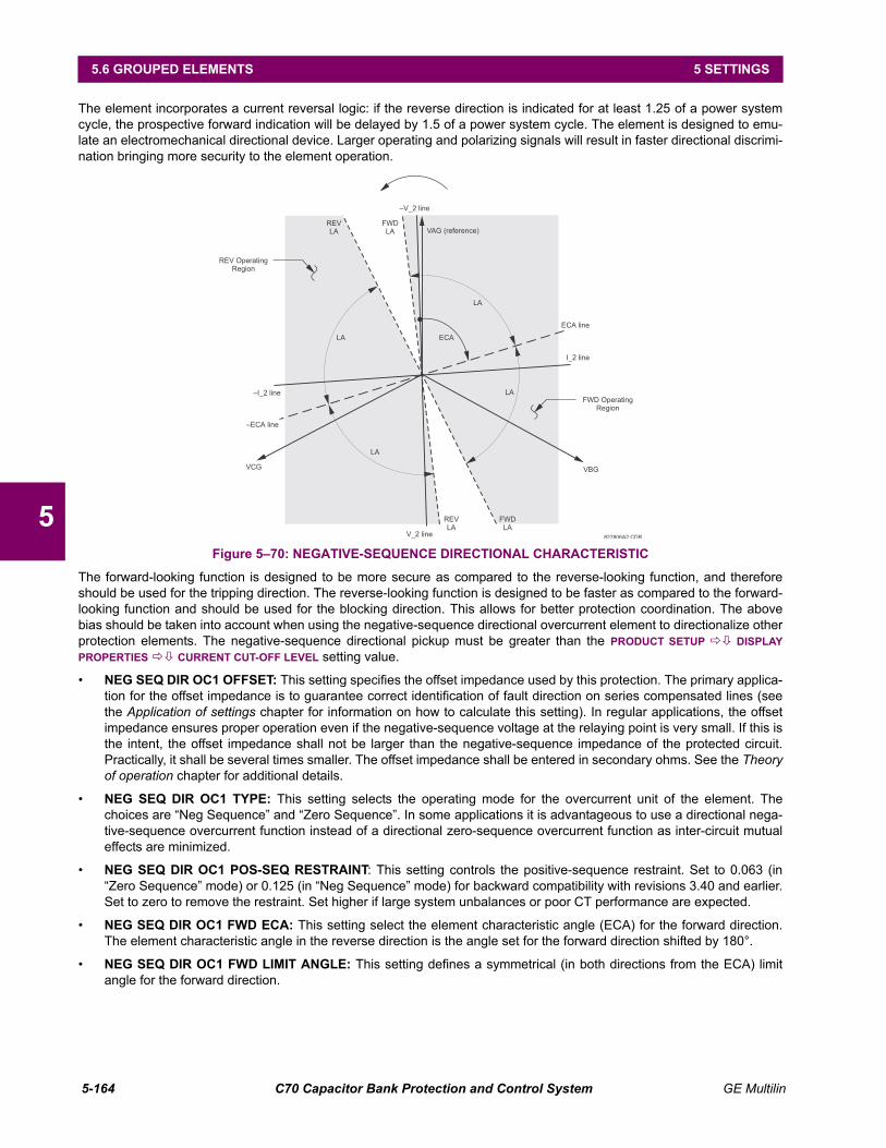
5-164 C70 Capacitor Bank Protection and Control System GE Multilin
5.6 GROUPED ELEMENTS 5 SETTINGS
5
The element incorporates a current reversal logic: if the reverse direction is indicated for at least 1.25 of a power systemcycle, the prospective forward indication will be delayed by 1.5 of a power system cycle. The element is designed to emu-late an electromechanical directional device. Larger operating and polarizing signals will result in faster directional discrimi-nation bringing more security to the element operation.
Figure 5–70: NEGATIVE-SEQUENCE DIRECTIONAL CHARACTERISTIC
The forward-looking function is designed to be more secure as compared to the reverse-looking function, and thereforeshould be used for the tripping direction. The reverse-looking function is designed to be faster as compared to the forward-looking function and should be used for the blocking direction. This allows for better protection coordination. The abovebias should be taken into account when using the negative-sequence directional overcurrent element to directionalize otherprotection elements. The negative-sequence directional pickup must be greater than the PRODUCT SETUP DISPLAY
PROPERTIES CURRENT CUT-OFF LEVEL setting value.
• NEG SEQ DIR OC1 OFFSET: This setting specifies the offset impedance used by this protection. The primary applica-tion for the offset impedance is to guarantee correct identification of fault direction on series compensated lines (seethe Application of settings chapter for information on how to calculate this setting). In regular applications, the offsetimpedance ensures proper operation even if the negative-sequence voltage at the relaying point is very small. If this isthe intent, the offset impedance shall not be larger than the negative-sequence impedance of the protected circuit.Practically, it shall be several times smaller. The offset impedance shall be entered in secondary ohms. See the Theoryof operation chapter for additional details.
• NEG SEQ DIR OC1 TYPE: This setting selects the operating mode for the overcurrent unit of the element. Thechoices are “Neg Sequence” and “Zero Sequence”. In some applications it is advantageous to use a directional nega-tive-sequence overcurrent function instead of a directional zero-sequence overcurrent function as inter-circuit mutualeffects are minimized.
• NEG SEQ DIR OC1 POS-SEQ RESTRAINT: This setting controls the positive-sequence restraint. Set to 0.063 (in“Zero Sequence” mode) or 0.125 (in “Neg Sequence” mode) for backward compatibility with revisions 3.40 and earlier.Set to zero to remove the restraint. Set higher if large system unbalances or poor CT performance are expected.
• NEG SEQ DIR OC1 FWD ECA: This setting select the element characteristic angle (ECA) for the forward direction.The element characteristic angle in the reverse direction is the angle set for the forward direction shifted by 180°.
• NEG SEQ DIR OC1 FWD LIMIT ANGLE: This setting defines a symmetrical (in both directions from the ECA) limitangle for the forward direction.
827806A2.CDR
VAG (reference)
VCG VBG
–I_2 line
I_2 line
ECA line
–ECA line
LA
LA
LA
LA ECA
FWD OperatingRegion
REV OperatingRegion
FWDLA
FWDLA
REVLA
REVLA
V_2 line
–V_2 line

GE Multilin C70 Capacitor Bank Protection and Control System 5-165
5 SETTINGS 5.6 GROUPED ELEMENTS
5
• NEG SEQ DIR OC1 FWD PICKUP: This setting defines the pickup level for the overcurrent unit in the forward direc-tion. Upon NEG SEQ DIR OC1 TYPE selection, this pickup threshold applies to zero- or negative-sequence current. Whenselecting this setting it must be kept in mind that the design uses a positive-sequence restraint technique.
• NEG SEQ DIR OC1 REV LIMIT ANGLE: This setting defines a symmetrical (in both directions from the ECA) limitangle for the reverse direction.
• NEG SEQ DIR OC1 REV PICKUP: This setting defines the pickup level for the overcurrent unit in the reverse direc-tion. Upon NEG SEQ DIR OC1 TYPE selection, this pickup threshold applies to zero- or negative-sequence current. Whenselecting this setting it must be kept in mind that the design uses a positive-sequence restraint technique.
Figure 5–71: NEGATIVE SEQUENCE DIRECTIONAL OC1 SCHEME LOGIC

5-166 C70 Capacitor Bank Protection and Control System GE Multilin
5.6 GROUPED ELEMENTS 5 SETTINGS
5
5.6.8 VOLTAGE ELEMENTS
a) MAIN MENU
PATH: SETTINGS GROUPED ELEMENTS SETTING GROUP 1(6) VOLTAGE ELEMENTS
These protection elements can be used for a variety of applications such as:
• Undervoltage Protection: For voltage sensitive loads, such as induction motors, a drop in voltage increases thedrawn current which may cause dangerous overheating in the motor. The undervoltage protection feature can be used
VOLTAGE ELEMENTS
PHASE UNDERVOLTAGE1
See page 5–168.
MESSAGE PHASE UNDERVOLTAGE2
See page 5–168.
MESSAGE PHASE OVERVOLTAGE1
See page 5–169.
MESSAGE NEUTRAL OV1
See page 5–170.
MESSAGE NEUTRAL OV2
See page 5–170.
MESSAGE NEUTRAL OV3
See page 5–170.
MESSAGE NEG SEQ OV1
See page 5–171.
MESSAGE NEG SEQ OV2
See page 5–171.
MESSAGE NEG SEQ OV3
See page 5–171.
MESSAGE AUXILIARY OV1
See page 5–172.
MESSAGE AUXILIARY OV2
See page 5–172.
MESSAGE AUXILIARY OV3
See page 5–172.
MESSAGE VOLTAGE DIFFERENTIAL 1
See page 5–173.
MESSAGE VOLTAGE DIFFERENTIAL 2
See page 5–173.
MESSAGE VOLTAGE DIFFERENTIAL 3
See page 5–173.
MESSAGE BANK OVERVOLTAGE
See page 5–176.
MESSAGE NEUTRAL VOLTAGE UNBALANCE 1
See page 5–180.
MESSAGE NEUTRAL VOLTAGE UNBALANCE 2
See page 5–180.
MESSAGE NEUTRAL VOLTAGE UNBALANCE 3
See page 5–180.

GE Multilin C70 Capacitor Bank Protection and Control System 5-167
5 SETTINGS 5.6 GROUPED ELEMENTS
5
to either cause a trip or generate an alarm when the voltage drops below a specified voltage setting for a specified timedelay.
• Permissive Functions: The undervoltage feature may be used to block the functioning of external devices by operat-ing an output relay when the voltage falls below the specified voltage setting. The undervoltage feature may also beused to block the functioning of other elements through the block feature of those elements.
• Source Transfer Schemes: In the event of an undervoltage, a transfer signal may be generated to transfer a loadfrom its normal source to a standby or emergency power source.
The undervoltage elements can be programmed to have a definite time delay characteristic. The definite time curve oper-ates when the voltage drops below the pickup level for a specified period of time. The time delay is adjustable from 0 to600.00 seconds in steps of 0.01. The undervoltage elements can also be programmed to have an inverse time delay char-acteristic.
The undervoltage delay setting defines the family of curves shown below.
(EQ 5.18)
where: T = operating timeD = undervoltage delay setting (D = 0.00 operates instantaneously)V = secondary voltage applied to the relayVpickup = pickup level
Figure 5–72: INVERSE TIME UNDERVOLTAGE CURVES
At 0% of pickup, the operating time equals the UNDERVOLTAGE DELAY setting.
T D
1 VVpickup------------------–
----------------------------------=
842788A1.CDR
% of voltage pickup
Tim
e(s
ec
on
ds)
NOTE

5-168 C70 Capacitor Bank Protection and Control System GE Multilin
5.6 GROUPED ELEMENTS 5 SETTINGS
5
b) PHASE UNDERVOLTAGE (ANSI 27P, IEC PTUV)
PATH: SETTINGS GROUPED ELEMENTS SETTING GROUP 1(6) VOLTAGE ELEMENTS PHASE UNDERVOLTAGE1(3)
This element may be used to give a desired time-delay operating characteristic versus the applied fundamental voltage(phase-to-ground or phase-to-phase for wye VT connection, or phase-to-phase for delta VT connection) or as a definitetime element. The element resets instantaneously if the applied voltage exceeds the dropout voltage. The delay settingselects the minimum operating time of the phase undervoltage. The minimum voltage setting selects the operating voltagebelow which the element is blocked (a setting of “0” will allow a dead source to be considered a fault condition).
Figure 5–73: PHASE UNDERVOLTAGE1 SCHEME LOGIC
PHASE UNDERVOLTAGE1
PHASE UV1FUNCTION: Disabled
Range: Disabled, Enabled
MESSAGEPHASE UV1 SIGNALSOURCE: SRC 1
Range: SRC 1, SRC 2
MESSAGEPHASE UV1 MODE:Phase to Ground
Range: Phase to Ground, Phase to Phase
MESSAGEPHASE UV1PICKUP: 1.000 pu
Range: 0.000 to 3.000 pu in steps of 0.001
MESSAGEPHASE UV1CURVE: Definite Time
Range: Definite Time, Inverse Time
MESSAGEPHASE UV1DELAY: 1.00 s
Range: 0.00 to 600.00 s in steps of 0.01
MESSAGEPHASE UV1 MINIMUMVOLTAGE: 0.100 pu
Range: 0.000 to 3.000 pu in steps of 0.001
MESSAGEPHASE UV1 BLOCK:Off
Range: FlexLogic operand
MESSAGEPHASE UV1TARGET: Self-reset
Range: Self-reset, Latched, Disabled
MESSAGEPHASE UV1EVENTS: Disabled
Range: Disabled, Enabled
PHASE UV1FUNCTION:
PHASE UV1BLOCK:
PHASE UV1 SOURCE:
PHASE UV1 MODE:
PHASE UV1PICKUP:
PHASE UV1CURVE:
PHASE UV1DELAY:
PHASE UV1MINIMUM VOLTAGE:
Disabled = 0
Off = 0
Source VT = Delta
Phase to Ground Phase to Phase
RUN
RUN
VCG or VCA PICKUP
VBG or VBC PICKUP
VAG or VAB Minimum
VBG or VBC Minimum
VCG or VCA Minimum
Source VT = Wye
VAG VAB
VBG VBC
VCG VCA
Enabled = 1
VAB
VBC
VCA
PHASE UV1 A PKP
PHASE UV1 B PKP
PHASE UV1 C PKP
PHASE UV1 PKP
PHASE UV1 A DPO
PHASE UV1 B DPO
PHASE UV1 C DPO
PHASE UV1 A OP
PHASE UV1 B OP
PHASE UV1 C OP
PHASE UV1 OP
AND
SETTING
SETTING
SETTING
SETTING
SETTING
SETTING
FLEXLOGIC OPERANDS
FLEXLOGIC OPERAND
FLEXLOGIC OPERAND
827039AB.CDR
AND
AND
AND
OR
OR
<
<
<
<
<
t
V
t
t
V
V
VAG or VAB PICKUP<RUN
PHASE UV1 DPO
FLEXLOGIC OPERAND
AND

GE Multilin C70 Capacitor Bank Protection and Control System 5-169
5 SETTINGS 5.6 GROUPED ELEMENTS
5
c) PHASE OVERVOLTAGE (ANSI 59P, IEC PTOV)
PATH: SETTINGS GROUPED ELEMENTS SETTING GROUP 1(6) VOLTAGE ELEMENTS PHASE OVERVOLTAGE1
The phase overvoltage element may be used as an instantaneous element with no intentional time delay or as a definitetime element. The input voltage is the phase-to-phase voltage, either measured directly from delta-connected VTs or as cal-culated from phase-to-ground (wye) connected VTs. The specific voltages to be used for each phase are shown below.
Figure 5–74: PHASE OVERVOLTAGE SCHEME LOGIC
If the source VT is wye-connected, then the phase overvoltage pickup condition is for VAB, VBC,and VCA.
PHASE OVERVOLTAGE1
PHASE OV1FUNCTION: Disabled
Range: Disabled, Enabled
MESSAGEPHASE OV1 SIGNALSOURCE: SRC 1
Range: SRC 1, SRC 2
MESSAGEPHASE OV1PICKUP: 1.000 pu
Range: 0.000 to 3.000 pu in steps of 0.001
MESSAGEPHASE OV1 PICKUPDELAY: 1.00 s
Range: 0.00 to 600.00 s in steps of 0.01
MESSAGEPHASE OV1 RESETDELAY: 1.00 s
Range: 0.00 to 600.00 s in steps of 0.01
MESSAGEPHASE OV1 BLOCK:Off
Range: FlexLogic Operand
MESSAGEPHASE OV1TARGET: Self-reset
Range: Self-reset, Latched, Disabled
MESSAGEPHASE OV1EVENTS: Disabled
Range: Disabled, Enabled
PHASE OV1
SOURCE:
Source VT = Delta
Source VT = Wye
VAB
VBC
VCA
PHASE OV1 A PKP
PHASE OV1 B PKP
PHASE OV1 C PKP
PHASE OV1 OP
PHASE OV1 A DPO
PHASE OV1 B DPO
PHASE OV1 C DPO
PHASE OV1 A OP
PHASE OV1 B OP
PHASE OV1 C OP
PHASE OV1 DPO
AND
PHASE OV1
FUNCTION:
Disabled = 0
Enabled = 1
SETTING
PHASE OV1
BLOCK:
Off = 0
SETTING
SETTING
PHASE OV1
PICKUP:
SETTING
FLEXLOGIC OPERANDS
FLEXLOGIC OPERAND
FLEXLOGIC OPERAND
827066A7.CDR
RUN
VAB PICKUP≥
RUN
VBC PICKUP≥
RUN
VCA PICKUP≥
AND
OR
PHASE OV1 PKP
FLEXLOGIC OPERAND
OR
PHASE OV1 RESET
DELAY:
SETTINGS
tPKP
tPKP
tPKP
tRST
tRST
tRST
PHASE OV1 PICKUP
DELAY:
NOTE
V 3 Pickup

5-170 C70 Capacitor Bank Protection and Control System GE Multilin
5.6 GROUPED ELEMENTS 5 SETTINGS
5
d) NEUTRAL OVERVOLTAGE (ANSI 59N, IEC PTOV)
PATH: SETTINGS GROUPED ELEMENTS SETTING GROUP 1(6) VOLTAGE ELEMENTS NEUTRAL OV1(3)
There are three neutral overvoltage elements available. The neutral overvoltage element can be used to detect asymmetri-cal system voltage condition due to a ground fault or to the loss of one or two phases of the source. The element respondsto the system neutral voltage (3V_0), calculated from the phase voltages. The nominal secondary voltage of the phase volt-age channels entered under SETTINGS SYSTEM SETUP AC INPUTS VOLTAGE BANK PHASE VT SECONDARY is thep.u. base used when setting the pickup level.
The neutral overvoltage element can provide a time-delayed operating characteristic versus the applied voltage (initializedfrom FlexCurves A, B, or C) or be used as a definite time element. The NEUTRAL OV1 PICKUP DELAY setting applies only ifthe NEUTRAL OV1 CURVE setting is “Definite time”. The source assigned to this element must be configured for a phase VT.
VT errors and normal voltage unbalance must be considered when setting this element. This function requires the VTs tobe wye-connected.
Figure 5–75: NEUTRAL OVERVOLTAGE1 SCHEME LOGIC
NEUTRAL OV1
NEUTRAL OV1FUNCTION: Disabled
Range: Disabled, Enabled
MESSAGENEUTRAL OV1 SIGNALSOURCE: SRC 1
Range: SRC 1, SRC 2
MESSAGENEUTRAL OV1 PICKUP:0.300 pu
Range: 0.000 to 3.000 pu in steps of 0.001
MESSAGENEUTRAL OV1 CURVE:Definite time
Range: Definite time, FlexCurve A, FlexCurve B,FlexCurve C
MESSAGENEUTRAL OV1 PICKUP:DELAY: 1.00 s
Range: 0.00 to 600.00 s in steps of 0.01
MESSAGENEUTRAL OV1 RESET:DELAY: 1.00 s
Range: 0.00 to 600.00 s in steps of 0.01
MESSAGENEUTRAL OV1 BLOCK:Off
Range: FlexLogic operand
MESSAGENEUTRAL OV1 TARGET:Self-reset
Range: Self-reset, Latched, Disabled
MESSAGENEUTRAL OV1 EVENTS:Disabled
Range: Disabled, Enabled

GE Multilin C70 Capacitor Bank Protection and Control System 5-171
5 SETTINGS 5.6 GROUPED ELEMENTS
5
e) NEGATIVE-SEQUENCE OVERVOLTAGE(ANSI 59Q, IEC PTOV)
PATH: SETTINGS GROUPED ELEMENTS SETTING GROUP 1(6) VOLTAGE ELEMENTS NEG SEQ OV1(3)
There is one negative-sequence overvoltage element available per CT bank, to a maximum of three.
The negative-sequence overvoltage element may be used to detect loss of one or two phases of the source, a reversedphase sequence of voltage, or a non-symmetrical system voltage condition.
Figure 5–76: NEGATIVE-SEQUENCE OVERVOLTAGE SCHEME LOGIC
NEG SEQ OV1
NEG SEQ OV1FUNCTION: Disabled
Range: Disabled, Enabled
MESSAGENEG SEQ OV1 SIGNALSOURCE: SRC 1
Range: SRC 1, SRC 2
MESSAGENEG SEQ OV1 PICKUP:0.300 pu
Range: 0.000 to 1.250 pu in steps of 0.001
MESSAGENEG SEQ OV1 PICKUPDELAY: 0.50 s
Range: 0.00 to 600.00 s in steps of 0.01
MESSAGENEG SEQ OV1 RESETDELAY: 0.50 s
Range: 0.00 to 600.00 s in steps of 0.01
MESSAGENEG SEQ OV1 BLOCK:Off
Range: FlexLogic operand
MESSAGENEG SEQ OV1 TARGET:Self-reset
Range: Self-reset, Latched, Disabled
MESSAGENEG SEQ OV1 EVENTS:Disabled
Range: Disabled, Enabled
SETTING
SETTINGS
FLEXLOGIC OPERANDS
SETTING
SETTING
NEG SEQ OV1
FUNCTION:
NEG SEQ OV1 RESET
DELAY:
NEG SEQ OV1 PICKUP
DELAY:
NEG SEQ OV1 PKP
NEG SEQ OV1 DPO
NEG SEQ OV1 OP
NEG SEQ OV1 BLOCK:
Disabled = 0
Off = 0
Enabled = 1
NEG SEQ OV1 SIGNAL
SOURCE:
Wye VT Delta VT
V_2827839A3.CDR
AND
SETTING
NEG SEQ OV1 PICKUP:
V_2 or 3 × V_2 PKP≥
RUN
t
tPKP
RST
3 × V_2

5-172 C70 Capacitor Bank Protection and Control System GE Multilin
5.6 GROUPED ELEMENTS 5 SETTINGS
5
f) AUXILIARY OVERVOLTAGE (ANSI 59X, IEC PTOV)
PATH: SETTINGS GROUPED ELEMENTS SETTING GROUP 1(6) VOLTAGE ELEMENTS AUXILIARY OV1(3)
The C70 contains one auxiliary overvoltage element for each VT bank. This element is intended for monitoring overvoltageconditions of the auxiliary voltage. The nominal secondary voltage of the auxiliary voltage channel entered under SYSTEM
SETUP AC INPUTS VOLTAGE BANK X5 AUXILIARY VT X5 SECONDARY is the per-unit (pu) base used when setting thepickup level.
Figure 5–77: AUXILIARY OVERVOLTAGE SCHEME LOGIC
AUXILIARY OV1
AUX OV1FUNCTION: Disabled
Range: Disabled, Enabled
MESSAGEAUX OV1 SIGNALSOURCE: SRC 1
Range: SRC 1, SRC 2
MESSAGEAUX OV1 PICKUP:0.300 pu
Range: 0.000 to 3.000 pu in steps of 0.001
MESSAGEAUX OV1 PICKUPDELAY: 1.00 s
Range: 0.00 to 600.00 s in steps of 0.01
MESSAGEAUX OV1 RESETDELAY: 1.00 s
Range: 0.00 to 600.00 s in steps of 0.01
MESSAGEAUX OV1 BLOCK:Off
Range: FlexLogic operand
MESSAGEAUX OV1 TARGET:Self-reset
Range: Self-reset, Latched, Disabled
MESSAGEAUX OV1 EVENTS:Disabled
Range: Disabled, Enabled
827836A2.CDR
FLEXLOGIC OPERANDS
AUX OV1FUNCTION:
AUX OV1 BLOCK:
AUX OV1 SIGNALSOURCE:
AUX OV1 PICKUP:
AUX OV1 DPO
AUX OV1 OP
AUX OV1 PKP
RUNAND
SETTING
SETTING
AUX OV1 RESETDELAY :
AUX OV1 PICKUPDELAY :
SETTING
Enabled=1
Disabled=0
tPKP
tRST
SETTING
SETTING
Off=0
AUXILIARY VOLT (Vx)
Vx Pickup<

GE Multilin C70 Capacitor Bank Protection and Control System 5-173
5 SETTINGS 5.6 GROUPED ELEMENTS
5
g) BANK VOLTAGE DIFFERENTIAL (ANSI 87V, IEC PDIF)
PATH: SETTINGS GROUPED ELEMENTS SETTING GROUP 1(6) VOLTAGE ELEMENTS VOLTAGE DIFFERENTIAL 1(3)
VOLTAGE DIFFERENTIAL 1
VOLTAGE DIF 1FUNCTION: Disabled
Range: Disabled, Enabled
MESSAGEVOLTAGE DIF 1 BUSSOURCE: SRC 1
Range: SRC 1, SRC 2, SRC 3, SRC 4, SRC 5, SRC 6
MESSAGEVOLTAGE DIF 1 TAPSOURCE: SRC 1
Range: SRC 1, SRC 2, SRC 3, SRC 4, SRC 5, SRC 6
MESSAGEVOLTAGE DIF 1 BANKGROUND: Grounded
Range: Grounded, Ungrounded
MESSAGEVOLTAGE DIF 1 MATCHFACTOR A: 2.0000
Range: 0.5000 to 2000.0000 in steps of 0.0001
MESSAGEVOLTAGE DIF 1 MATCHFACTOR B: 2.0000
Range: 0.5000 to 2000.0000 in steps of 0.0001
MESSAGEVOLTAGE DIF 1 MATCHFACTOR C: 2.0000
Range: 0.5000 to 2000.0000 in steps of 0.0001
MESSAGEVOLTAGE DIF 1 STG 1APICKUP: 0.010 pu
Range: 0.001 to 1.000 pu in steps of 0.001
MESSAGEVOLTAGE DIF 1 STG 2APICKUP: 0.020 pu
Range: 0.001 to 1.000 pu in steps of 0.001
MESSAGEVOLTAGE DIF 1 STG 3APICKUP: 0.030 pu
Range: 0.001 to 1.000 pu in steps of 0.001
MESSAGEVOLTAGE DIF 1 STG 4APICKUP: 0.040 pu
Range: 0.001 to 1.000 pu in steps of 0.001
MESSAGEVOLTAGE DIF 1 STG 1BPICKUP: 0.010 pu
Range: 0.001 to 1.000 pu in steps of 0.001
MESSAGEVOLTAGE DIF 1 STG 2BPICKUP: 0.020 pu
Range: 0.001 to 1.000 pu in steps of 0.001
MESSAGEVOLTAGE DIF 1 STG 3BPICKUP: 0.030 pu
Range: 0.001 to 1.000 pu in steps of 0.001
MESSAGEVOLTAGE DIF 1 STG 4BPICKUP: 0.040 pu
Range: 0.001 to 1.000 pu in steps of 0.001
MESSAGEVOLTAGE DIF 1 STG 1CPICKUP: 0.010 pu
Range: 0.001 to 1.000 pu in steps of 0.001
MESSAGEVOLTAGE DIF 1 STG 2CPICKUP: 0.020 pu
Range: 0.001 to 1.000 pu in steps of 0.001
MESSAGEVOLTAGE DIF 1 STG 3CPICKUP: 0.030 pu
Range: 0.001 to 1.000 pu in steps of 0.001
MESSAGEVOLTAGE DIF 1 STG 4CPICKUP: 0.040 pu
Range: 0.001 to 1.000 pu in steps of 0.001
MESSAGEVOLTAGE DIF 1 STG 1PKP DELAY: 30.00 s
Range: 0.00 to 600.00 s in steps of 0.01
MESSAGEVOLTAGE DIF 1 STG 2PKP DELAY: 10.00 s
Range: 0.00 to 600.00 s in steps of 0.01

5-174 C70 Capacitor Bank Protection and Control System GE Multilin
5.6 GROUPED ELEMENTS 5 SETTINGS
5Up to three identical voltage differential elements, one per each VT bank configured in hardware, are provided.
The element responds to a differential signal between magnitudes of the bus and tap voltages. The latter is scaled using amatching factor to account for the position of the tap. An automatic setting procedure is available under the COMMAND
menu to calculate automatically the matching factor when installing the relay or after repairs of the bank.
Figure 5–78: VOLTAGE DIFFERENTIAL BASIC CONNECTIONS
The function works with grounded and ungrounded banks. In the latter case, the neutral point voltage must be measured bythe relay. For additional information, refer to the Theory of Operation and Application of Settings chapters.
The following settings are available for each voltage differential element.
MESSAGEVOLTAGE DIF 1 STG 3PKP DELAY: 1.00 s
Range: 0.00 to 600.00 s in steps of 0.01
MESSAGEVOLTAGE DIF 1 STG 4PKP DELAY: 0.20 s
Range: 0.00 to 600.00 s in steps of 0.01
MESSAGEVOLTAGE DIF 1DPO DELAY: 0.25 s
Range: 0.00 to 600.00 s in steps of 0.01
MESSAGEVOLT DIF 1 BLK STG1:Off
Range: FlexLogic operand
MESSAGEVOLT DIF 1 BLK STG 2:Off
Range: FlexLogic operand
MESSAGEVOLT DIF 1 BLK STG 3:Off
Range: FlexLogic operand
MESSAGEVOLT DIF 1 BLK STG 4:Off
Range: FlexLogic operand
MESSAGEVOLT DIF 1 TARGET:Self-Reset
Range: Self-reset, Latched, Disabled
MESSAGEVOLT DIF 1 EVENTS:Disabled
Range: Disabled, Enabled
C70 CAPACITOR BANK RELAY
87V
BUS
SOURCE
TAP
SOURCE
Phase
VT bank
Aux VT
For ungrounded
banks only
Phase
VT bank
834738A1.CDR

GE Multilin C70 Capacitor Bank Protection and Control System 5-175
5 SETTINGS 5.6 GROUPED ELEMENTS
5
• VOLTAGE DIF 1 BUS SOURCE: Indicate signal source that signifies the bus voltage of the bank. The function usesthis source as reference for pu settings of pickup thresholds, and scales the tap voltages to this signal level. The VTratio and secondary nominal voltage are set under separate menu. Voltages of this source must be connected in wyefor the function to operate.
• VOLTAGE DIF 1 TAP SOURCE: Indicate signal source that signifies the tap voltage of the bank. The function scalesthis voltage to the bus level using the matching factor setting. The matching is performed on primary voltages, or perunit of the bus voltage. The VT ratio and secondary nominal voltage are set under separate menu. Voltages of thissource must be connected in wye for the function to operate. If this function is used on ungrounded banks, the tapsource must have the neutral point voltage of the bank configured under the auxiliary voltage channel. That auxiliaryvoltage must be labelled “Vn” under the VT setup menu.
• VOLTAGE DIF 1 BANK GROUND: Indicate if the protected bank is grounded or ungrounded. In the latter case, theauxiliary voltage configured under the tap source will be subtracted from the phase voltages of both the bus and tap.This results in the actual voltage drop along the capacitor string, and thus facilitates the voltage differential principle.The relay automatically compensates for different VT ratios and secondary voltages of the neutral point voltage andthe bus and tap voltages.
• VOLTAGE DIF 1 MATCH FACTOR A to VOLTAGE DIF 1 MATCH FACTOR C: This setting specifies the division ratioof the healthy bank, i.e. the ratio between the bus and tap voltages (value greater than 1). The matching factor isapplied as multiplier for the primary tap voltage before comparing with the primary bus voltage. Quality of balancing thebank with a given value of this setting can be viewed under ACTUAL VALUES menu. An automatic setting procedure isavailable under the COMMANDS menu to calculate the matching factors automatically.
• VOLTAGE DIF 1 STG 1A PICKUP to VOLTAGE DIF 1 STG 4C PICKUP: These settings specify pickup thresholds forstages 1 through 4 for phases A to C in per-units (pu) of the nominal bus voltage. A value of 1 pu is a product of thenominal secondary voltage and VT ratio of the voltage bank configured under the bus source of this function. Fourindependent stages are provided for each phase of protection.
• VOLTAGE DIF 1 STG 1 PKP DELAY: This setting specifies the pickup time delay, individually per each stage of alarm-ing/tripping. Note that each of the twelve comparators (four stages in three phases) uses an individual timer, but set-tings for these timers are controlled individually per each stage, not per phase. The timers use a common drop out timedelay specified by the next setting.
• VOLTAGE DIF 1 DPO DELAY: This setting controls a drop out delay for the operate FlexLogic operands. Note thatindividual stages apply individually configurable pickup delays, but use this common drop out delay.
• VOLT DIF 1 BLK STG 1 to VOLT DIF 1 BLK STG 4: These inputs are used to block the function on a per stage basiswhen required. At minimum this function shall be blocked when the bank is off-line, or else it will operate unnecessarily.Either breaker position or undercurrent indication via any available instantaneous function, or a combination, may beused for blocking. The VT fuse fail condition from both the bus and tap VT should also be considered. Note that whenunblocked, the function becomes operational after five cycles of intentional delay.

5-176 C70 Capacitor Bank Protection and Control System GE Multilin
5.6 GROUPED ELEMENTS 5 SETTINGS
5
Figure 5–79: VOLTAGE DIFFERENTIAL SCHEME LOGIC
h) BANK PHASE OVERVOLTAGE (ANSI 59B, IEC PTOV)
PATH: SETTINGS GROUPED... SETTING GROUP 1(6) VOLTAGE... BANK OVERVOLTAGE BANK OVERVOLTAGE 1
BANK OVERVOLTAGE 1
BANK OV 1FUNCTION: Disabled
Range: Disabled, Enabled
MESSAGEBANK OV 1 BUSSOURCE: SRC 1
Range: SRC 1, SRC 2, SRC 3, SRC 4, SRC 5, SRC 6
MESSAGEBANK OV 1 NTRLSOURCE: SRC 1
Range: SRC 1, SRC 2, SRC 3, SRC 4, SRC 5, SRC 6
MESSAGEBANK OV 1 BANKGROUND: Grounded
Range: Grounded, Ungrounded, Ungr w/o Vn
MESSAGEBANK OV 1 CURVE:FlexCurve A
Range: FlexCurve A, FlexCurve B, FlexCurve C,FlexCurve D
MESSAGEBANK OV 1 CURVE TIMEMULTIPLIER: 1.00
Range: 1.00 to 10.00 in steps of 0.01
MESSAGEBANK OV 1 STG 1APICKUP: 1.050 pu
Range: 0.800 to 2.000 pu in steps of 0.001
tPKP
t DPO
tPKP
tDPO
tPKP
tDPO
SETTINGS
VOLTAGE DIF 1 BUS
SOURCE:
V1A
V1B
V1C
VOLTAGE DIF 1 TAP
SOURCE:
V2A
V2B
V2C
VN
SETTINGS
VA
_d
if=
|V
A_
ma
g-
kA
*V
2A
_m
ag
|
or
|V
A_
ma
g-
kA
*(V
2A
-V
N)_
ma
g|
VOLTAGE DIF 1
MATCH FACTOR A:
SETTING
VOLTAGE DIF 1 STG
1A PICKUP:
SETTING
VOLTAGE DIF 1 STG
2A PICKUP:
SETTING
VOLTAGE DIF 1 STG
3A PICKUP:
SETTING
VOLTAGE DIF 1 STG
4A PICKUP:
VOLT DIF 1 STG 1A PKP
FLEXLOGIC OPERAND
VOLT DIF 1 STG 2A PKP
FLEXLOGIC OPERAND
VOLT DIF 1 STG 3A PKP
FLEXLOGIC OPERAND
VOLT DIF 1 STG 4A PKP
FLEXLOGIC OPERAND
tPKP
tDPO
TIMERS
VOLTAGE DIF 1 STG 1
PKP DELAY:
VOLTAGE DIF 1 STG 2
PKP DELAY:
VOLTAGE DIF 1 STG 3
PKP DELAY:
VOLTAGE DIF 1 STG 4
PKP DELAY:
VOLT DIF 1 STG 1A OP
VOLT DIF 1 STG 2A OP
VOLT DIF 1 STG 3A OP
FLEXLOGIC OPERAND
VOLT DIF 1 STG 4A OP
VOLT DIF 1 PKP B
VOLTAGE DIF 1 DPO
DELAY:
VOLT DIF 1 PKP A
VOLT DIF 1 PKP C
OR
VOLT DIF 1 PKPOR
VOLT DIF 1 OP B
VOLT DIF 1 OP A
VOLT DIF 1 OP C
OR
VOLT DIF 1 OPOR
VOLT DIF 1 DPO
PHASE C
5 cycles
0
TIMER
RUN 87V FUNCTION
PHASE B
COMMANDS
AUTO-SETTING
PROCEDURE
VOLTAGE DIF 1 BANK
GROUND:
SETTING
COMMANDS/
VOLTAGE DIF 1
AUTO-SETTING:
WRITE A NEW SETTING
AN
D
VC_mag > 0.25 pu
VB_mag > 0.25 pu
VA_mag > 0.25 pu
SETTINGS
VOLTAGE DIF 1
FUNCTION:
Enabled = 1
VOLT DIF 1 BLK STG1:
Off = 0
VOLT DIF 1 BLK STG2:
Off = 0
VOLT DIF 1 BLK STG3:
Off = 0
VOLT DIF 1 BLK STG4:
Off = 0
AN
D
INHIBIT STAGE 1
INHIBIT STAGE 3
INHIBIT STAGE 4
INHIBIT STAGE 2
AN
D
Manual
Auto AN
D
Apply?
FLEXLOGIC OPERAND
FLEXLOGIC OPERAND
FLEXLOGIC OPERAND
FLEXLOGIC OPERAND
FLEXLOGIC OPERANDFLEXLOGIC OPERAND
FLEXLOGIC OPERAND
VA_dif > PICKUP
RUNAN
D
VA_dif > PICKUP
RUNAN
D
VA_dif > PICKUP
RUNAN
D
VA_dif > PICKUP
RUNAN
D
834742A1.DWG

GE Multilin C70 Capacitor Bank Protection and Control System 5-177
5 SETTINGS 5.6 GROUPED ELEMENTS
5
Up to three identical bank overvoltage elements, one per each VT bank configured in hardware, are provided.
The bank phase overvoltage element responds to voltages across the capacitors of the bank. Three stages of definite timeoperation, and one stage of inverse time operation are provided. Pickup thresholds of this function are adjustable on a per-phase basis. The shape of the inverse time curve is user-programmable (via FlexCurves) with individual pickup levels anda multiplier common for all three phases. The definite time delays are individually programmable per stage.
The function works with grounded and ungrounded banks. With ungrounded banks, either the neutral point voltage is mea-sured by the relay and used to derive the true bank voltage based on the bus and neutral-point voltages, or a simplifiedmethod to provide proper voltage protection is used responding to vector differences between the phase-to-phase voltages.
MESSAGEBANK OV 1 STG 2APICKUP: 1.100 pu
Range: 0.800 to 2.000 pu in steps of 0.001
MESSAGEBANK OV 1 STG 3APICKUP: 1.200 pu
Range: 0.800 to 2.000 pu in steps of 0.001
MESSAGEBANK OV 1 STG 4APICKUP: 1.050 pu
Range: 0.800 to 2.000 pu in steps of 0.001
MESSAGEBANK OV 1 STG 1BPICKUP: 1.050 pu
Range: 0.800 to 2.000 pu in steps of 0.001
MESSAGEBANK OV 1 STG 2BPICKUP: 1.100 pu
Range: 0.800 to 2.000 pu in steps of 0.001
MESSAGEBANK OV 1 STG 3BPICKUP: 1.200 pu
Range: 0.800 to 2.000 pu in steps of 0.001
MESSAGEBANK OV 1 STG 4BPICKUP: 1.050 pu
Range: 0.800 to 2.000 pu in steps of 0.001
MESSAGEBANK OV 1 STG 1CPICKUP: 1.050 pu
Range: 0.800 to 2.000 pu in steps of 0.001
MESSAGEBANK OV 1 STG 2CPICKUP: 1.100 pu
Range: 0.800 to 2.000 pu in steps of 0.001
MESSAGEBANK OV 1 STG 3CPICKUP: 1.200 pu
Range: 0.800 to 2.000 pu in steps of 0.001
MESSAGEBANK OV 1 STG 4CPICKUP: 1.050 pu
Range: 0.800 to 2.000 pu in steps of 0.001
MESSAGEBANK OV 1 STG 1PKP DELAY: 60.00 s
Range: 0.00 to 600.00 s in steps of 0.01
MESSAGEBANK OV 1 STG 2PKP DELAY: 10.00 s
Range: 0.00 to 600.00 s in steps of 0.01
MESSAGEBANK OV 1 STG 3PKP DELAY: 2.00 s
Range: 0.00 to 600.00 s in steps of 0.01
MESSAGEBANK OV 1 STG 4PKP DELAY: 0.20 s
Range: 0.00 to 600.00 s in steps of 0.01
MESSAGEBANK OV 1 DPO DELAY:0.25 s
Range: 0.00 to 600.00 s in steps of 0.01
MESSAGEBANK OV 1 BLK:Off
Range: FlexLogic operand
MESSAGEBANK OV 1 TARGET:Self-Reset
Range: Self-reset, Latched, Disabled
MESSAGEBANK OV 1 EVENTS:Disabled
Range: Disabled, Enabled

5-178 C70 Capacitor Bank Protection and Control System GE Multilin
5.6 GROUPED ELEMENTS 5 SETTINGS
5
When fed from wye-connected VTs, thus function responds to phase-to-ground voltages. When fed from delta-connectedVTs, this function responds to the vector difference between the phase-to-phase voltages.
The function responds to true RMS voltages to account for effects of harmonics (harmonics impacting losses in the capaci-tor, harmonics increasing peak values in the voltages compared with the filtered fundamental frequency magnitudes).
Figure 5–80: BANK OVERVOLTAGE BASIC CONNECTIONS
For more information refer to the Theory of Operation and Application of Settings chapters. The following settings are avail-able for each bank phase overvoltage element.
• BANK OV 1 BUS SOURCE: This setting indicates the signal source that signifies the bus voltage of the capacitorbank. The function uses this source as reference for per-unit (pu) settings of the pickup thresholds. The VT ratio andsecondary nominal voltage are set under the SETTINGS SYSTEM SETUP AC INPUTS VOLTAGE BANK menu.
• BANK OV 1 NTRL SOURCE: This setting indicates the signal source that signifies the neutral-point voltage of thebank. The auxiliary voltage channel of this source is used, and must be labelled “Vn” under the VT setup menu. Theneutral point voltage is used only when the function is applied to an ungrounded bank, to derive the true voltage dropacross the capacitors. The VT ratio and secondary nominal voltage are set under the SETTINGS SYSTEM SETUP AC INPUTS VOLTAGE BANK menu.
• BANK OV 1 BANK GROUND: This setting indicates if the protected bank is grounded, ungrounded with the neutralpoint voltage measured, and ungrounded without the neutral point voltage. The relay automatically compensates forpotentially different VT ratios and secondary voltages of the bus and neutral point voltages. The following tableexplains the operating signals of the function based on the input signals available to the relay.
VT CONNECTION
BANK CONFIGURATION
GROUNDED UNGROUNDED UNGROUNDED W/O VN
Wye Vop_A = VAVop_B = VBVop_C = VC
Vop_A = VA – VXVop_B = VB – VXVop_C = VC – VX
Vop_A = (VCA – VAB) / 3Vop_B = (VAB – VBC) / 3Vop_C = (VBC – VCA) / 3
Delta Vop_A = (VCA – VAB) / 3Vop_B = (VAB – VBC) / 3Vop_C = (VBC – VCA) / 3
Alternative: delta
connected VTs
C70 CAPACITOR BANK RELAY
59B
BUS
SRC
NTRL
SRC
Phase
VT Bank
Aux VT
For ungrounded
banks only
834734A1.DWG

GE Multilin C70 Capacitor Bank Protection and Control System 5-179
5 SETTINGS 5.6 GROUPED ELEMENTS
5
• BANK OV 1 CURVE: This setting specifies a FlexCurve used by the fourth inverse time stage of this function. Flex-Curves are user-programmable on a point-by-point basis. This function applies a common curve shape in all threephases. However, the curve is specified as time versus multiple of pickup. With three individually programmable pickupvalues per phase one accommodates possible differences between individual phases of the bank even though a com-mon curve shape is used.
Implementation of the inverse-time stage is based on the concept of a virtual disk emulating electromechanical relays.When above the pickup level, the function integrates towards the trip level at the rate dictated by the curve at a givenmultiple of pickup. When activated but with the operating signal below the pickup, the function integrates down towarda complete reset. This mode of operation assures dependability in situations when the voltage oscillates and causesstress to the protected capacitor in repetitive cycles each lasting too short to expire a straight timer. As a result of thisimplementation, the shape of the curve below multiple of pickup of 1 is important as it controls the speed of reset of apartially energized function.
• BANK OV 1 STG 1A PICKUP to BANK OV 1 STG 3C PICKUP: These settings specify pickup thresholds for stages 1through 3 in phases A through C in per-units (pu) of the nominal phase-to-ground bus voltage. A value of 1 pu is aproduct of the nominal secondary voltage and VT ratio of the voltage bank configured under the bus source of thisfunction. With a delta VT configuration, a value of 1 pu is a product of the nominal secondary voltage and VT ratiodivided by . Three independent stages of definite-time operation are provided for each phase of the bank.
• BANK OV 1 STG 4A PICKUP to BANK OV 1 STG 4C PICKUP: These settings specify pickup thresholds for theinverse time stage 4 in phase A through C in per-units (pu) of the nominal phase-to-ground bus voltage. With a wye VTconfiguration, a value of 1 pu is a product of the nominal secondary voltage and VT ratio of the voltage bank configuredunder the bus source of this function. With a delta VT configuration, a value of 1 pu is a product of the nominal second-ary voltage and VT ratio divided by . The inverse time stage uses a user-programmable FlexCurve selected by theBANK OV 1 CURVE setting.
• BANK OV 1 STG 1 PKP DELAY to BANK OV 1 STG 3 PKP DELAY: These settings specify the pickup time delays foreach definite time stage of alarming/tripping. Note that each of the nine comparators (three definite-time stages inthree phases) uses an individual timer, but settings for these timers are controlled individually per each stage, not perphase. The timers use a common dropout time delay specified by the BANK OV 1 DPO DELAY setting.
• BANK OV 1 DPO DELAY: This setting controls a dropout delay for the operate FlexLogic operands. Note that individ-ual stages apply individually configurable pickup delays, but use this common dropout delay.
• BANK OV 1 BLK: This input is used to block the function when required; in particular, when the bank is offline.
3
3
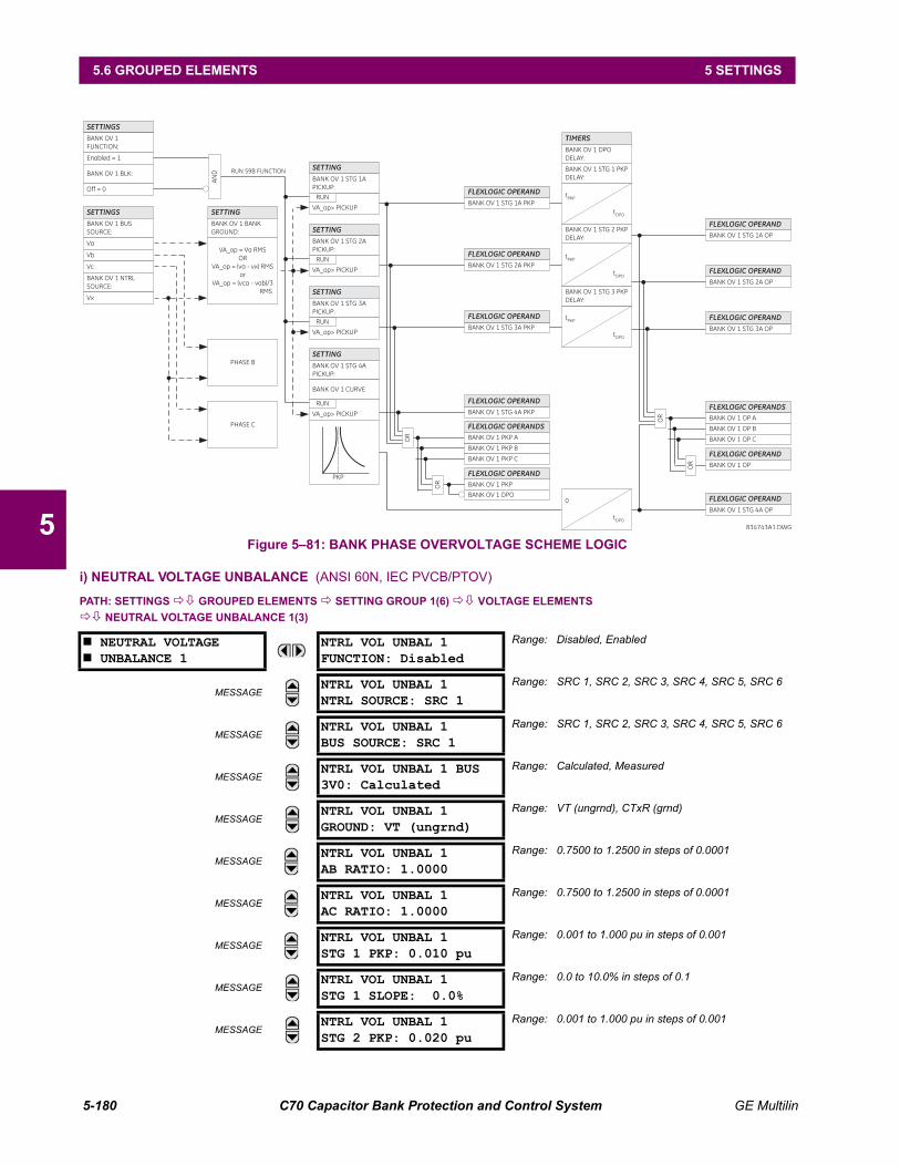
5-180 C70 Capacitor Bank Protection and Control System GE Multilin
5.6 GROUPED ELEMENTS 5 SETTINGS
5Figure 5–81: BANK PHASE OVERVOLTAGE SCHEME LOGIC
i) NEUTRAL VOLTAGE UNBALANCE (ANSI 60N, IEC PVCB/PTOV)
PATH: SETTINGS GROUPED ELEMENTS SETTING GROUP 1(6) VOLTAGE ELEMENTS
NEUTRAL VOLTAGE UNBALANCE 1(3)
NEUTRAL VOLTAGE UNBALANCE 1
NTRL VOL UNBAL 1FUNCTION: Disabled
Range: Disabled, Enabled
MESSAGENTRL VOL UNBAL 1NTRL SOURCE: SRC 1
Range: SRC 1, SRC 2, SRC 3, SRC 4, SRC 5, SRC 6
MESSAGENTRL VOL UNBAL 1BUS SOURCE: SRC 1
Range: SRC 1, SRC 2, SRC 3, SRC 4, SRC 5, SRC 6
MESSAGENTRL VOL UNBAL 1 BUS3V0: Calculated
Range: Calculated, Measured
MESSAGENTRL VOL UNBAL 1GROUND: VT (ungrnd)
Range: VT (ungrnd), CTxR (grnd)
MESSAGENTRL VOL UNBAL 1AB RATIO: 1.0000
Range: 0.7500 to 1.2500 in steps of 0.0001
MESSAGENTRL VOL UNBAL 1AC RATIO: 1.0000
Range: 0.7500 to 1.2500 in steps of 0.0001
MESSAGENTRL VOL UNBAL 1STG 1 PKP: 0.010 pu
Range: 0.001 to 1.000 pu in steps of 0.001
MESSAGENTRL VOL UNBAL 1STG 1 SLOPE: 0.0%
Range: 0.0 to 10.0% in steps of 0.1
MESSAGENTRL VOL UNBAL 1STG 2 PKP: 0.020 pu
Range: 0.001 to 1.000 pu in steps of 0.001
tPKP
tDPO
tPKP
tDPO
SETTINGS
BANK OV 1 BUS
SOURCE:
Va
Vb
Vc
BANK OV 1 NTRL
SOURCE:
Vx
AN
DSETTING
VA_op = Va RMS
OR
VA_op = (va - vx) RMS
or
VA_op = (vca - vab)/3
RMS
VA_op> PICKUP
SETTING
BANK OV 1 STG 1A
PICKUP:
SETTING
BANK OV 1 STG 2A
PICKUP:
SETTING
BANK OV 1 STG 3A
PICKUP:
SETTING
BANK OV 1 STG 4A
PICKUP:
BANK OV 1 STG 1A PKP
FLEXLOGIC OPERAND
BANK OV 1 STG 2A PKP
FLEXLOGIC OPERAND
BANK OV 1 STG 3A PKP
FLEXLOGIC OPERAND
BANK OV 1 STG 4A PKP
FLEXLOGIC OPERAND
tPKP
tDPO
TIMERS
BANK OV 1 STG 1 PKP
DELAY:
BANK OV 1 STG 2 PKP
DELAY:
BANK OV 1 STG 3 PKP
DELAY:
BANK OV 1 STG 1A OP
FLEXLOGIC OPERAND
BANK OV 1 STG 2A OP
FLEXLOGIC OPERAND
BANK OV 1 STG 3A OP
FLEXLOGIC OPERAND
BANK OV 1 STG 4A OP
FLEXLOGIC OPERAND
BANK OV 1 PKP B
FLEXLOGIC OPERANDS
BANK OV 1 DPO
DELAY:
BANK OV 1 PKP A
BANK OV 1 PKP C
OR
FLEXLOGIC OPERAND
BANK OV 1 PKPOR
BANK OV 1 OP B
FLEXLOGIC OPERANDS
BANK OV 1 OP A
BANK OV 1 OP C
OR
FLEXLOGIC OPERAND
BANK OV 1 OPOR
BANK OV 1 DPO
PHASE C
SETTINGS
BANK OV 1
FUNCTION:
Enabled = 1
BANK OV 1 BLK:
Off = 0
RUN 59B FUNCTION
PHASE B
BANK OV 1 BANK
GROUND:
BANK OV 1 CURVE
PKP
RUN
VA_op> PICKUP
VA_op> PICKUP
VA_op> PICKUP
RUN
RUN
RUN
834743A1.DWG
0
tDPO
GE Multilin C70 Capacitor Bank Protection and Control System 5-181
5 SETTINGS 5.6 GROUPED ELEMENTS
5
Up to three identical neutral voltage unbalance elements, one per each VT bank configured in hardware, are provided.
The element responds to the voltage signal at the neutral point of the capacitor bank. The operating equations are properlycompensated for both the system unbalance such as during close-in external faults, and the inherent bank unbalance. Thebus zero-sequence voltage required for compensation of the system unbalance can be measured internally to the relayfrom phase voltages, or delivered as a 3V0 signal from an open-corner-delta VT via an auxiliary voltage channel of therelay.
Compensation for the inherent unbalance of the protected bank uses the B and C phase voltages, and thus this functionrequires wye connected phase VTs. The inherent unbalance is zeroed out using ratios of the reactances between the refer-ence phase A, and the two other phases. An automatic setting procedure is available under the COMMAND menu to calcu-late the compensating factors automatically when installing the relay, or after repairs of the bank.
To enhance performance under large system unbalances when the neutral-point and system zero-sequence voltages maybecome significant, a concept of a restraint is introduced. The slope of the operating characteristic is user adjustable, and ifdesired, it can be effectively removed yielding a straight compensated overvoltage function.
For additional information refer to the Theory of operation and Application of settings chapters.
MESSAGENTRL VOL UNBAL 1STG 2 SLOPE: 0.0%
Range: 0.0 to 10.0% in steps of 0.1
MESSAGENTRL VOL UNBAL 1STG 3 PKP: 0.020 pu
Range: 0.001 to 1.000 pu in steps of 0.001
MESSAGENTRL VOL UNBAL 1STG 3 SLOPE: 5.0%
Range: 0.0 to 10.0% in steps of 0.1
MESSAGENTRL VOL UNBAL 1STG 4 PKP: 0.030 pu
Range: 0.001 to 1.000 pu in steps of 0.001
MESSAGENTRL VOL UNBAL 1STG 4 SLOPE: 5.0%
Range: 0.0 to 10.0% in steps of 0.1
MESSAGENTRL VOL UNBAL 1 STG1 PKP DELAY: 30.00 s
Range: 0.00 to 600.00 s in steps of 0.01
MESSAGENTRL VOL UNBAL 1 STG2 PKP DELAY: 10.00 s
Range: 0.00 to 600.00 s in steps of 0.01
MESSAGENTRL VOL UNBAL 1 STG3 PKP DELAY: 1.00 s
Range: 0.00 to 600.00 s in steps of 0.01
MESSAGENTRL VOL UNBAL 1 STG4 PKP DELAY: 0.20 s
Range: 0.00 to 600.00 s in steps of 0.01
MESSAGENTRL VOL UNBAL 1DPO DELAY: 0.25 s
Range: 0.00 to 600.00 s in steps of 0.01
MESSAGENTRL VOL 1 BLK STG1:Off
Range: FlexLogic operand
MESSAGENTRL VOL 1 BLK STG2:Off
Range: FlexLogic operand
MESSAGENTRL VOL 1 BLK STG3:Off
Range: FlexLogic operand
MESSAGENTRL VOL 1 BLK STG4:Off
Range: FlexLogic operand
MESSAGENTRL VOL UNBAL 1TARGET: Self-Reset
Range: Self-reset, Latched, Disabled
MESSAGENTRL VOL UNBAL 1EVENTS: Disabled
Range: Disabled, Enabled

5-182 C70 Capacitor Bank Protection and Control System GE Multilin
5.6 GROUPED ELEMENTS 5 SETTINGS
5Figure 5–82: NEUTRAL VOLTAGE UNBALANCE BASIC CONNECTION
The following settings are available for all three neutral voltage unbalance elements.
• NTRL VOL UNBAL 1 NTRL SOURCE: Indicate signal source that signifies the neutral-point voltage of the protectedbank. This single-phase voltage is to be configured under the auxiliary VT channel. The VT ratio and secondary nomi-nal voltage are set under separate menu. Nominal voltage of this auxiliary channel becomes a unit (1 pu) for the pickupsettings of this function.
• NTRL VOL UNBAL 1 BUS SOURCE: Indicate signal source that signifies the bus voltages of the bank. This sourcemust have the phase voltages configured in order to facilitate compensation for the inherent unbalance of the bank.The zero-sequence voltage required for system unbalance compensation can be derived from the phase voltages, ordelivered to the relay from an external source, typically a broken-delta VT (the selection is controlled by the next set-ting of this function). In the latter case, the 3V0 signal is expected and must be wired and configured under the auxiliaryvoltage channel of this source. This 3V0 voltage must be labelled as “Vn” under the VT configuration. The VT ratio andsecondary nominal voltage are set under separate menu. Phase voltages of this source must be connected in wye forthe function to operate. The function uses several voltages potentially produced by VTs of different ratios and nominalsecondary values. The relay scales all the signals automatically for meaningful calculations.
• NTRL VOL UNBAL 1 BUS 3V0: This setting specifies the source of the bus zero-sequence voltage required for sys-tem unbalance compensation. If set to “Calculated”, the relay would derive the zero-sequence voltage as a vector sumof the three phase voltages and will run the function if voltage in all three phases is greater than 0.25 pu. If set to “Mea-sured”, the relay expects the 3V0 signal (not a V0) to be wired to the relay under the auxiliary channel of the bussource, and labelled as “Vn”. In this case, the voltage check to run this function is not performed.
• NTRL VOL UNBAL 1 GROUND: This setting selects the grounding arrangement of the bank. For ungrounded banks itshould be set to “VT (ungrnd)”. When the bank neutral is solidly grounded through the CT with a resistor in the CT sec-ondary, then this setting should be chosen as “CTxR (grnd)”.
When the “CTxR (grnd)” value is selected, the measured bank neutral point voltage is shifted by 90° lagging to com-pensate for the angular difference between the bus neutral voltage and the voltage derived from the bank neutral pointcurrent. The value of resistor R should be chosen so the voltage measured by the auxiliary input of the relay matchesbus V0 during system faults (for example, an SLG fault at the bus). This is accomplished by the following condition:

GE Multilin C70 Capacitor Bank Protection and Control System 5-183
5 SETTINGS 5.6 GROUPED ELEMENTS
5
(EQ 5.19)
The terms used in the above equation are defined as follows.
– V0BUS is the bus primary zero-sequence voltage during system fault.
– 3I0NTRL is the primary current in the bank neutral during system fault.
– nBUS_VT is the bus VT ratio set in the source selected by the NTRL VOL UNBAL 1 BUS SOURCE setting.
– nNTRL_VT is a neutral point VT ratio set in the source selected by the NTRL VOL UNBAL 1 NTRL SOURCE setting. If Rcan be chosen precisely, then nNTRL_VT can be set same as nBUS_VT. If R cannot be chosen precisely, thennNTRL_VT is used to match zero-sequence voltage as per the equation above.
– nNTRL_CT is the CT ratio in the bank neutral.
• NTRL VOL UNBAL 1 AB RATIO: This setting compensates for the bank inherent unbalance. Physically this value is aratio of the reactance in phase A divided by the reactance in phase B. Auto-setting procedure is available under theCommands menu to calculate this value automatically. When tuning this setting manually, after bank repairs, this ratioshall be increased or decreased from the nominal value of 1.00 depending on whether the A or B phase got affected byfailures or repairs and whether a given reactance increased or decreased as a result of the failure or repair. This set-ting should only be used when NTRL VOL UNBAL 1 BUS 3V0 setting is set as “Calculated”.
• NTRL VOL UNBAL 1 AC RATIO: This setting compensates for the bank inherent unbalance. Physically this value is aratio of the reactance in phase A divided by the reactance in phase C. Auto-setting procedure is available under theCommands menu to calculate this value automatically. When tuning this setting manually, after bank repairs, this ratioshall be increased or decreased from the nominal value of 1.00 depending on whether the A or C phase got affectedby failures or repairs and whether a given reactance increased or decreased as a result of the failure or repair. Thissetting should only be used when NTRL VOL UNBAL 1 BUS 3V0 setting is set as “Calculated”.
• NTRL VOL UNBAL 1 STG 1 PKP to NTRL VOL UNBAL 1 STG 1 PKP: These settings specify pickup thresholds forstages 1 through 4 of the function in per-units (pu) of the nominal value of the neutral-point VT (the auxiliary channel ofthe neutral source).
• NTRL VOL UNBAL 1 STG 1 SLOPE to NTRL VOL UNBAL 1 STG 4 SLOPE: These settings specify the slopes of theoperating characteristic. Neglecting compensation for the inherent bank unbalance, the operating signal is a vectorialdifference between the neutral point voltage and the zero-sequence bus voltage. Therefore, the optimum restrainingsignal is a vectorial sum of the two signals. During external ground faults, the two voltages are approximately in phasegenerating a large restraining signal being twice the zero-sequence voltage at the bus. A slope of few percent is typi-cally sufficient to provide good security under large system unbalances. If a given stage is used with a time delay lon-ger than the expected external fault duration, the slope may be reduced or eliminated. In general, the slope can beunderstood as a adaptive threshold, and the user is provided with three ways to control sensitivity and security: pickup,time delay and slope. Refer to the Application of settings chapter for more information.
• NTRL VOL UNBAL 1 STG 1 PKP DELAY to NTRL VOL UNBAL 1 STG 4 PKP DELAY: These settings specify thepickup time delays for each stage of alarming or tripping. Note that each of the four comparators (four stages) uses anindividual pickup timer, but a common drop out time delay as specified by the next setting.
• NTRL VOL UNBAL 1 DPO DELAY: This setting controls a drop out delay for the operate FlexLogic operands. Notethat individual stages apply individually configurable pickup delays, but use this common drop out delay.
• NTRL VOL 1 BLK STG1 to NTRL VOL 1 BLK STG4: These settings are used to block the function when required ona per-stage basis. At minimum this function shall be blocked when the bank is off-line, or else it will operate unneces-sarily during external ground faults and/or natural system unbalance if set sensitive. Either breaker position or under-current indication via any available instantaneous overcurrent function, or a combination, may be used for blocking.Note that when unblocked, the function becomes operational after five cycles of intentional delay. Optionally only thesensitive stages are blocked, and one stage set high enough to ride through possible problems is left operational. Thisstage can be used for abnormal conditions such as a failure of one pole of the breaker to close. The function becomesblocked if all four blocking inputs are asserted. The individual blocking inputs inhibit the associated stages of the func-tion.
3V0BUS
nBUS_VT---------------------
3I0NTRL R nNTRL_VTnNTRL_CT nBUS_VT
-------------------------------------------------------------– 0=

5-184 C70 Capacitor Bank Protection and Control System GE Multilin
5.6 GROUPED ELEMENTS 5 SETTINGS
5
Figure 5–83: NEUTRAL VOLTAGE UNBALANCE LOGIC
tPKP
t DPO
SETTINGS
NTRL VOL UNBAL 1
BUS SOURCE:
VA
VB
VC
NTRL VOL UNBAL 1
NTRL SOURCE:
VX (Vn)
AN
D
VC_mag > 0.25 pu
VB_mag > 0.25 pu
VA_mag > 0.25 pu
SETTINGS
Vo
p=
|(1
+kA
B+
kA
C)*
Vn
-3
V0
+(1
-ka
b)*
VB
+(1
-kA
C)*
VC
|
/3
Vre
st
=|3
*V
n+
3V
0|/
3
NTRL VOL UNBAL 1
BUS 3V0:
SETTINGS
NTRL VOL UNBAL 1
STG 1 PKP:
NTRL VOLT 1 STG1 PKP
FLEXLOGIC OPERAND
TIMER
NTRL VOL UNBAL 1
STG 4 PKP DELAY:
NTRL VOLT 1 STG1 OP
FLEXLOGIC OPERAND
NTRL VOLT 1 STG2 OP
FLEXLOGIC OPERAND
NTRL VOLT 1 STG3 OP
FLEXLOGIC OPERAND
NTRL VOL UNBAL 1
DPO DELAY:
SETTINGS
NTRL VOL UNBAL 1
FUNCTION:
Enabled = 1
NTRL VOL 1 BLK STG1:
Off = 05 cycles
0
TIMER
RUN 59NU FUNCTION
COMMANDS
AUTO-SETTING
PROCEDURE
AN
D
SETTING
COMMANDS/ NTRL
VOL UNBAL 1 AUTO
SET:
Manual
WRITE A NEW SETTING
V0 or VX (3V0)
NTRL VOL UNBAL 1
AC RATIO:
NTRL VOL UNBAL 1
AB RATIO:NTRL VOL UNBAL 1
STG 1 SLOPE:
SETTINGS
NTRL VOL UNBAL 1
STG 2 PKP:
NTRL VOL UNBAL 1
STG 2 SLOPE:
SETTINGS
NTRL VOL UNBAL 1
STG 3 PKP:
NTRL VOL UNBAL 1
STG 3 SLOPE:
SETTINGS
NTRL VOL UNBAL 1
STG 4 PKP:
NTRL VOL UNBAL 1
STG 4 SLOPE:
NTRL VOLT 1 STG2 PKP
FLEXLOGIC OPERAND
NTRL VOLT 1 STG3 PKP
FLEXLOGIC OPERAND
NTRL VOLT 1 STG4 PKP
FLEXLOGIC OPERAND
tPKP
tDPO
NTRL VOL UNBAL 1
STG 3 PKP DELAY:
tPKP
tDPO
NTRL VOL UNBAL 1
STG 2 PKP DELAY:
tPKP
tDPO
NTRL VOL UNBAL 1
STG 1 PKP DELAY:
NTRL VOLT 1 STG4 OP
FLEXLOGIC OPERAND
NTRL VOL UNBAL 1
DPO DELAY:
TIMER
NTRL VOL UNBAL 1
DPO DELAY:
TIMER
NTRL VOL UNBAL 1
DPO DELAY:
TIMER
OR
FLEXLOGIC OPERANDS
NTRL VOLT 1 PKP
NTRL VOLT 1 DPO
OR
FLEXLOGIC OPERANDS
NTRL VOLT 1 OP
NTRL VOL 1 BLK STG2:
Off = 0
NTRL VOL 1 BLK STG3:
Off = 0
NTRL VOL 1 BLK STG4:
Off = 0
AN
D
INHIBIT STAGE 1
INHIBIT STAGE 3
INHIBIT STAGE 4
INHIBIT STAGE 2
Apply?
Auto AN
D
RUN
RUN
RUN
RUN
AN
DA
ND
AN
DA
ND
834741A1.DWG
GE Multilin C70 Capacitor Bank Protection and Control System 5-185
5 SETTINGS 5.7 CONTROL ELEMENTS
5
5.7CONTROL ELEMENTS 5.7.1 OVERVIEW
Control elements are generally used for control rather than protection. See the Introduction to Elements section at thebeginning of this chapter for further information.
5.7.2 TRIP BUS
PATH: SETTINGS CONTROL ELEMENTS TRIP BUS TRIP BUS 1(6)
The trip bus element allows aggregating outputs of protection and control elements without using FlexLogic and assigningthem a simple and effective manner. Each trip bus can be assigned for either trip or alarm actions. Simple trip conditioningsuch as latch, delay, and seal-in delay are available.
The easiest way to assign element outputs to a trip bus is through the EnerVista UR Setup software A protection summaryis displayed by navigating to a specific protection or control protection element and checking the desired bus box. Once thedesired element is selected for a specific bus, a list of element operate-type operands are displayed and can be assignedto a trip bus. If more than one operate-type operand is required, it may be assigned directly from the trip bus menu.
TRIP BUS 1
TRIP BUS 1FUNCTION: Disabled
Range: Enabled, Disabled
MESSAGETRIP BUS 1 BLOCK:Off
Range: FlexLogic operand
MESSAGETRIP BUS 1 PICKUPDELAY: 0.00 s
Range: 0.00 to 600.00 s in steps of 0.01
MESSAGETRIP BUS 1 RESETDELAY: 0.00 s
Range: 0.00 to 600.00 s in steps of 0.01
MESSAGETRIP BUS 1 INPUT 1:Off
Range: FlexLogic operand
MESSAGETRIP BUS 1 INPUT 2:Off
Range: FlexLogic operand
MESSAGETRIP BUS 1 INPUT 16:Off
Range: FlexLogic operand
MESSAGETRIP BUS 1LATCHING: Disabled
Range: Enabled, Disabled
MESSAGETRIP BUS 1 RESET:Off
Range: FlexLogic operand
MESSAGETRIP BUS 1 TARGET:Self-reset
Range: Self-reset, Latched, Disabled
MESSAGETRIP BUS 1EVENTS: Disabled
Range: Enabled, Disabled
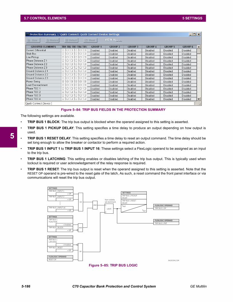
5-186 C70 Capacitor Bank Protection and Control System GE Multilin
5.7 CONTROL ELEMENTS 5 SETTINGS
5
Figure 5–84: TRIP BUS FIELDS IN THE PROTECTION SUMMARY
The following settings are available.
• TRIP BUS 1 BLOCK: The trip bus output is blocked when the operand assigned to this setting is asserted.
• TRIP BUS 1 PICKUP DELAY: This setting specifies a time delay to produce an output depending on how output isused.
• TRIP BUS 1 RESET DELAY: This setting specifies a time delay to reset an output command. The time delay should beset long enough to allow the breaker or contactor to perform a required action.
• TRIP BUS 1 INPUT 1 to TRIP BUS 1 INPUT 16: These settings select a FlexLogic operand to be assigned as an inputto the trip bus.
• TRIP BUS 1 LATCHING: This setting enables or disables latching of the trip bus output. This is typically used whenlockout is required or user acknowledgement of the relay response is required.
• TRIP BUS 1 RESET: The trip bus output is reset when the operand assigned to this setting is asserted. Note that theRESET OP operand is pre-wired to the reset gate of the latch, As such, a reset command the front panel interface or viacommunications will reset the trip bus output.
Figure 5–85: TRIP BUS LOGIC
**
*
SETTINGS
= Off
TRIP BUS 1 INPUT 2
= Off
TRIP BUS 1 INPUT 1
= Off
TRIP BUS 1 INPUT 16
OR
SETTINGS
= Enabled
TRIP BUS 1
FUNCTION
= Off
TRIP BUS 1 BLOCK AND
AND
Latch
S
R
Non-volatile,
set-dominant
SETTINGS
= Enabled
TRIP BUS 1
LATCHING
= Off
TRIP BUS 1 RESET
FLEXLOGIC OPERAND
TRIP BUS 1 PKP
OR
SETTINGS
TRIP BUS 1 PICKUP
DELAY
TRIP BUS 1 RESET
DELAY
TPKP
TRST
FLEXLOGIC OPERAND
RESET OP
FLEXLOGIC OPERAND
TRIP BUS 1 OP
842023A1.CDR

GE Multilin C70 Capacitor Bank Protection and Control System 5-187
5 SETTINGS 5.7 CONTROL ELEMENTS
5
5.7.3 SETTING GROUPS
PATH: SETTINGS CONTROL ELEMENTS SETTINGS GROUPS
The setting groups menu controls the activation and deactivation of up to six possible groups of settings in the GROUPED
ELEMENTS settings menu. The faceplate Settings In Use LEDs indicate which active group (with a non-flashing energizedLED) is in service.
The SETTING GROUPS BLK setting prevents the active setting group from changing when the FlexLogic parameter is set to"On". This can be useful in applications where it is undesirable to change the settings under certain conditions, such as thebreaker being open.
The GROUP 2 ACTIVATE ON to GROUP 6 ACTIVATE ON settings select a FlexLogic operand which, when set, will make the par-ticular setting group active for use by any grouped element. A priority scheme ensures that only one group is active at agiven time – the highest-numbered group which is activated by its ACTIVATE ON parameter takes priority over the lower-numbered groups. There is no activate on setting for group 1 (the default active group), because group 1 automaticallybecomes active if no other group is active.
The SETTING GROUP 1 NAME to SETTING GROUP 6 NAME settings allows to user to assign a name to each of the six settingsgroups. Once programmed, this name will appear on the second line of the GROUPED ELEMENTS SETTING GROUP 1(6)
menu display.
The relay can be set up via a FlexLogic equation to receive requests to activate or de-activate a particular non-default set-tings group. The following FlexLogic equation (see the figure below) illustrates requests via remote communications (forexample, VIRTUAL INPUT 1 ON) or from a local contact input (for example, CONTACT IP 1 ON) to initiate the use of a particu-lar settings group, and requests from several overcurrent pickup measuring elements to inhibit the use of the particular set-tings group. The assigned VIRTUAL OUTPUT 1 operand is used to control the “On” state of a particular settings group.
SETTING GROUPS
SETTING GROUPSFUNCTION: Disabled
Range: Disabled, Enabled
MESSAGESETTING GROUPS BLK:Off
Range: FlexLogic operand
MESSAGEGROUP 2 ACTIVATE ON:Off
Range: FlexLogic operand
MESSAGEGROUP 3 ACTIVATE ON:Off
Range: FlexLogic operand
MESSAGEGROUP 6 ACTIVATE ON:Off
Range: FlexLogic operand
MESSAGEGROUP 1 NAME: Range: up to 16 alphanumeric characters
MESSAGEGROUP 2 NAME: Range: up to 16 alphanumeric characters
MESSAGEGROUP 6 NAME: Range: up to 16 alphanumeric characters
MESSAGESETTING GROUPEVENTS: Disabled
Range: Disabled, Enabled
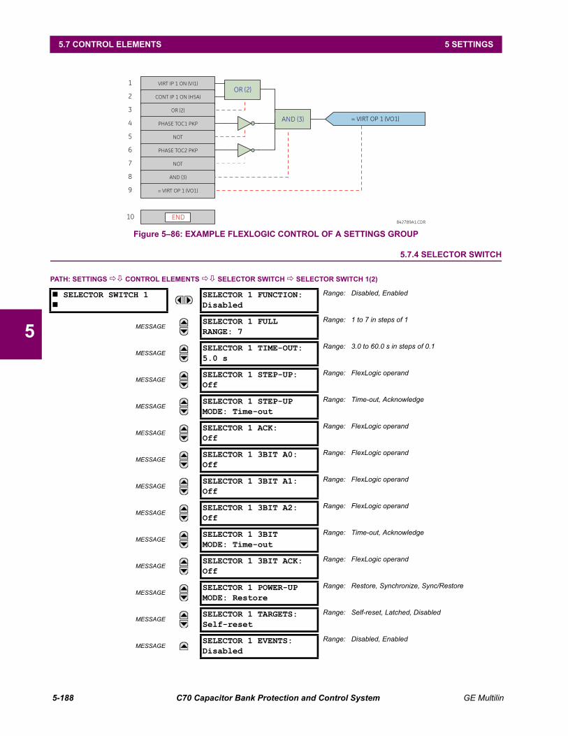
5-188 C70 Capacitor Bank Protection and Control System GE Multilin
5.7 CONTROL ELEMENTS 5 SETTINGS
5
Figure 5–86: EXAMPLE FLEXLOGIC CONTROL OF A SETTINGS GROUP
5.7.4 SELECTOR SWITCH
PATH: SETTINGS CONTROL ELEMENTS SELECTOR SWITCH SELECTOR SWITCH 1(2)
SELECTOR SWITCH 1
SELECTOR 1 FUNCTION:Disabled
Range: Disabled, Enabled
MESSAGESELECTOR 1 FULLRANGE: 7
Range: 1 to 7 in steps of 1
MESSAGESELECTOR 1 TIME-OUT:5.0 s
Range: 3.0 to 60.0 s in steps of 0.1
MESSAGESELECTOR 1 STEP-UP:Off
Range: FlexLogic operand
MESSAGESELECTOR 1 STEP-UPMODE: Time-out
Range: Time-out, Acknowledge
MESSAGESELECTOR 1 ACK:Off
Range: FlexLogic operand
MESSAGESELECTOR 1 3BIT A0:Off
Range: FlexLogic operand
MESSAGESELECTOR 1 3BIT A1:Off
Range: FlexLogic operand
MESSAGESELECTOR 1 3BIT A2:Off
Range: FlexLogic operand
MESSAGESELECTOR 1 3BITMODE: Time-out
Range: Time-out, Acknowledge
MESSAGESELECTOR 1 3BIT ACK:Off
Range: FlexLogic operand
MESSAGESELECTOR 1 POWER-UPMODE: Restore
Range: Restore, Synchronize, Sync/Restore
MESSAGESELECTOR 1 TARGETS:Self-reset
Range: Self-reset, Latched, Disabled
MESSAGESELECTOR 1 EVENTS:Disabled
Range: Disabled, Enabled
10
1 VIRT IP 1 ON (VI1)
2 CONT IP 1 ON (H5A)
3
OR (2)
OR (2)
4 PHASE TOC1 PKP
5 NOT
6 PHASE TOC2 PKP
7 NOT
8
AND (3)
AND (3)
9
= VIRT OP 1 (VO1)
= VIRT OP 1 (VO1)
END842789A1.CDR

GE Multilin C70 Capacitor Bank Protection and Control System 5-189
5 SETTINGS 5.7 CONTROL ELEMENTS
5
The selector switch element is intended to replace a mechanical selector switch. Typical applications include setting groupcontrol or control of multiple logic sub-circuits in user-programmable logic.
The element provides for two control inputs. The step-up control allows stepping through selector position one step at atime with each pulse of the control input, such as a user-programmable pushbutton. The three-bit control input allows set-ting the selector to the position defined by a three-bit word.
The element allows pre-selecting a new position without applying it. The pre-selected position gets applied either after time-out or upon acknowledgement via separate inputs (user setting). The selector position is stored in non-volatile memory.Upon power-up, either the previous position is restored or the relay synchronizes to the current three-bit word (user set-ting). Basic alarm functionality alerts the user under abnormal conditions; for example, the three-bit control input being outof range.
• SELECTOR 1 FULL RANGE: This setting defines the upper position of the selector. When stepping up through avail-able positions of the selector, the upper position wraps up to the lower position (position 1). When using a direct three-bit control word for programming the selector to a desired position, the change would take place only if the control wordis within the range of 1 to the SELECTOR FULL RANGE. If the control word is outside the range, an alarm is establishedby setting the SELECTOR ALARM FlexLogic operand for 3 seconds.
• SELECTOR 1 TIME-OUT: This setting defines the time-out period for the selector. This value is used by the relay inthe following two ways. When the SELECTOR STEP-UP MODE is “Time-out”, the setting specifies the required period ofinactivity of the control input after which the pre-selected position is automatically applied. When the SELECTOR STEP-
UP MODE is “Acknowledge”, the setting specifies the period of time for the acknowledging input to appear. The timer isre-started by any activity of the control input. The acknowledging input must come before the SELECTOR 1 TIME-OUT
timer expires; otherwise, the change will not take place and an alarm will be set.
• SELECTOR 1 STEP-UP: This setting specifies a control input for the selector switch. The switch is shifted to a newposition at each rising edge of this signal. The position changes incrementally, wrapping up from the last (SELECTOR 1
FULL RANGE) to the first (position 1). Consecutive pulses of this control operand must not occur faster than every50 ms. After each rising edge of the assigned operand, the time-out timer is restarted and the SELECTOR SWITCH 1:POS Z CHNG INITIATED target message is displayed, where Z the pre-selected position. The message is displayed forthe time specified by the FLASH MESSAGE TIME setting. The pre-selected position is applied after the selector times out(“Time-out” mode), or when the acknowledging signal appears before the element times out (“Acknowledge” mode).When the new position is applied, the relay displays the SELECTOR SWITCH 1: POSITION Z IN USE message. Typically,a user-programmable pushbutton is configured as the stepping up control input.
• SELECTOR 1 STEP-UP MODE: This setting defines the selector mode of operation. When set to “Time-out”, theselector will change its position after a pre-defined period of inactivity at the control input. The change is automatic anddoes not require any explicit confirmation of the intent to change the selector's position. When set to “Acknowledge”,the selector will change its position only after the intent is confirmed through a separate acknowledging signal. If theacknowledging signal does not appear within a pre-defined period of time, the selector does not accept the changeand an alarm is established by setting the SELECTOR STP ALARM output FlexLogic operand for 3 seconds.
• SELECTOR 1 ACK: This setting specifies an acknowledging input for the stepping up control input. The pre-selectedposition is applied on the rising edge of the assigned operand. This setting is active only under “Acknowledge” mode ofoperation. The acknowledging signal must appear within the time defined by the SELECTOR 1 TIME-OUT setting after thelast activity of the control input. A user-programmable pushbutton is typically configured as the acknowledging input.
• SELECTOR 1 3BIT A0, A1, and A2: These settings specify a three-bit control input of the selector. The three-bit con-trol word pre-selects the position using the following encoding convention:
A2 A1 A0 POSITION
0 0 0 rest
0 0 1 1
0 1 0 2
0 1 1 3
1 0 0 4
1 0 1 5
1 1 0 6
1 1 1 7
5-190 C70 Capacitor Bank Protection and Control System GE Multilin
5.7 CONTROL ELEMENTS 5 SETTINGS
5
The “rest” position (0, 0, 0) does not generate an action and is intended for situations when the device generating thethree-bit control word is having a problem. When SELECTOR 1 3BIT MODE is “Time-out”, the pre-selected position isapplied in SELECTOR 1 TIME-OUT seconds after the last activity of the three-bit input. When SELECTOR 1 3BIT MODE is“Acknowledge”, the pre-selected position is applied on the rising edge of the SELECTOR 1 3BIT ACK acknowledginginput.
The stepping up control input (SELECTOR 1 STEP-UP) and the three-bit control inputs (SELECTOR 1 3BIT A0 through A2)lock-out mutually: once the stepping up sequence is initiated, the three-bit control input is inactive; once the three-bitcontrol sequence is initiated, the stepping up input is inactive.
• SELECTOR 1 3BIT MODE: This setting defines the selector mode of operation. When set to “Time-out”, the selectorchanges its position after a pre-defined period of inactivity at the control input. The change is automatic and does notrequire explicit confirmation to change the selector position. When set to “Acknowledge”, the selector changes its posi-tion only after confirmation via a separate acknowledging signal. If the acknowledging signal does not appear within apre-defined period of time, the selector rejects the change and an alarm established by invoking the SELECTOR BITALARM FlexLogic operand for 3 seconds.
• SELECTOR 1 3BIT ACK: This setting specifies an acknowledging input for the three-bit control input. The pre-selected position is applied on the rising edge of the assigned FlexLogic operand. This setting is active only under the“Acknowledge” mode of operation. The acknowledging signal must appear within the time defined by the SELECTOR
TIME-OUT setting after the last activity of the three-bit control inputs. Note that the stepping up control input and three-bit control input have independent acknowledging signals (SELECTOR 1 ACK and SELECTOR 1 3BIT ACK, accordingly).
• SELECTOR 1 POWER-UP MODE: This setting specifies the element behavior on power up of the relay.
When set to “Restore”, the last position of the selector (stored in the non-volatile memory) is restored after powering upthe relay. If the position restored from memory is out of range, position 0 (no output operand selected) is applied andan alarm is set (SELECTOR 1 PWR ALARM).
When set to “Synchronize” selector switch acts as follows. For two power cycles, the selector applies position 0 to theswitch and activates SELECTOR 1 PWR ALARM. After two power cycles expire, the selector synchronizes to the positiondictated by the three-bit control input. This operation does not wait for time-out or the acknowledging input. When thesynchronization attempt is unsuccessful (that is, the three-bit input is not available (0,0,0) or out of range) then theselector switch output is set to position 0 (no output operand selected) and an alarm is established (SELECTOR 1 PWRALARM).
The operation of “Synch/Restore” mode is similar to the “Synchronize” mode. The only difference is that after anunsuccessful synchronization attempt, the switch will attempt to restore the position stored in the relay memory. The“Synch/Restore” mode is useful for applications where the selector switch is employed to change the setting group inredundant (two relay) protection schemes.
• SELECTOR 1 EVENTS: If enabled, the following events are logged:
EVENT NAME DESCRIPTION
SELECTOR 1 POS Z Selector 1 changed its position to Z.
SELECTOR 1 STP ALARM The selector position pre-selected via the stepping up control input has not been confirmed before the time out.
SELECTOR 1 BIT ALARM The selector position pre-selected via the three-bit control input has not been confirmed before the time out.

GE Multilin C70 Capacitor Bank Protection and Control System 5-191
5 SETTINGS 5.7 CONTROL ELEMENTS
5
The following figures illustrate the operation of the selector switch. In these diagrams, “T” represents a time-out setting.
Figure 5–87: TIME-OUT MODE
842737A1.CDR
STEP-UP
3BIT A0
3BIT A1
3BIT A2
POS 1
POS 2
POS 3
POS 4
POS 5
POS 6
POS 7
BIT 0
BIT 1
BIT 2
pre-existing
position 2
changed to 4 with
a pushbutton
changed to 1 with
a 3-bit input
changed to 2 with a
pushbutton
T T
T T
changed to 7 with
a 3-bit input
STP ALARM
BIT ALARM
ALARM
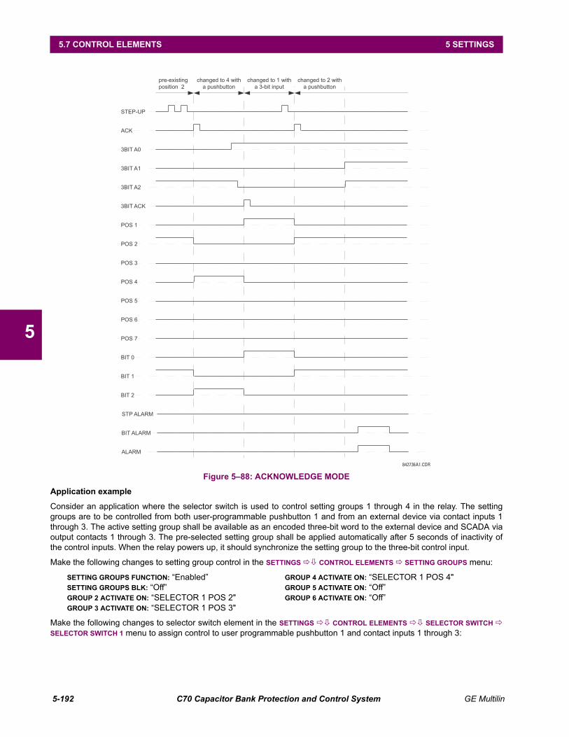
5-192 C70 Capacitor Bank Protection and Control System GE Multilin
5.7 CONTROL ELEMENTS 5 SETTINGS
5
Figure 5–88: ACKNOWLEDGE MODE
Application example
Consider an application where the selector switch is used to control setting groups 1 through 4 in the relay. The settinggroups are to be controlled from both user-programmable pushbutton 1 and from an external device via contact inputs 1through 3. The active setting group shall be available as an encoded three-bit word to the external device and SCADA viaoutput contacts 1 through 3. The pre-selected setting group shall be applied automatically after 5 seconds of inactivity ofthe control inputs. When the relay powers up, it should synchronize the setting group to the three-bit control input.
Make the following changes to setting group control in the SETTINGS CONTROL ELEMENTS SETTING GROUPS menu:
SETTING GROUPS FUNCTION: “Enabled” GROUP 4 ACTIVATE ON: “SELECTOR 1 POS 4"SETTING GROUPS BLK: “Off” GROUP 5 ACTIVATE ON: “Off”GROUP 2 ACTIVATE ON: “SELECTOR 1 POS 2" GROUP 6 ACTIVATE ON: “Off”GROUP 3 ACTIVATE ON: “SELECTOR 1 POS 3"
Make the following changes to selector switch element in the SETTINGS CONTROL ELEMENTS SELECTOR SWITCH SELECTOR SWITCH 1 menu to assign control to user programmable pushbutton 1 and contact inputs 1 through 3:
842736A1.CDR
STEP-UP
ACK
3BIT A0
3BIT A1
3BIT A2
3BIT ACK
POS 1
POS 2
POS 3
POS 4
POS 5
POS 6
POS 7
BIT 0
BIT 1
BIT 2
pre-existing
position 2
changed to 4 with
a pushbutton
changed to 1 with
a 3-bit input
changed to 2 with
a pushbutton
STP ALARM
BIT ALARM
ALARM

GE Multilin C70 Capacitor Bank Protection and Control System 5-193
5 SETTINGS 5.7 CONTROL ELEMENTS
5
SELECTOR 1 FUNCTION: “Enabled” SELECTOR 1 3BIT A0: “CONT IP 1 ON”SELECTOR 1 FULL-RANGE: “4” SELECTOR 1 3BIT A1: “CONT IP 2 ON”SELECTOR 1 STEP-UP MODE: “Time-out” SELECTOR 1 3BIT A2: “CONT IP 3 ON”SELECTOR 1 TIME-OUT: “5.0 s” SELECTOR 1 3BIT MODE: “Time-out”SELECTOR 1 STEP-UP: “PUSHBUTTON 1 ON” SELECTOR 1 3BIT ACK: “Off”SELECTOR 1 ACK: “Off” SELECTOR 1 POWER-UP MODE: “Synchronize”
Now, assign the contact output operation (assume the H6E module) to the selector switch element by making the followingchanges in the SETTINGS INPUTS/OUTPUTS CONTACT OUTPUTS menu:
OUTPUT H1 OPERATE: “SELECTOR 1 BIT 0"OUTPUT H2 OPERATE: “SELECTOR 1 BIT 1"OUTPUT H3 OPERATE: “SELECTOR 1 BIT 2"
Finally, assign configure user-programmable pushbutton 1 by making the following changes in the SETTINGS PRODUCT
SETUP USER-PROGRAMMABLE PUSHBUTTONS USER PUSHBUTTON 1 menu:
PUSHBUTTON 1 FUNCTION: “Self-reset”PUSHBUTTON 1 DROP-OUT TIME: “0.10 s”
The logic for the selector switch is shown below:
Figure 5–89: SELECTOR SWITCH LOGIC
842012A2.CDR
step up
acknowledge
3-bit position out
ON
FLEXLOGIC™ OPERANDS
SELECTOR 1 POS 1
SELECTOR 1 POS 2
SELECTOR 1 POS 3
SELECTOR 1 POS 4
SELECTOR 1 POS 5
SELECTOR 1 POS 6
SELECTOR 1 POS 7
SELECTOR 1 STP ALARM
SELECTOR 1 BIT ALARM
SELECTOR 1 ALARM
SELECTOR 1 BIT 0
SELECTOR 1 BIT 1
SELECTOR 1 BIT 2
FLEXLOGIC™ OPERANDS
RUN
SELECTOR 1 POWER-UP MODE:
SETTINGS
SELECTOR 1 TIME-OUT:
SELECTOR 1 STEP-UP MODE:
SELECTOR 1 FULL RANGE:
SELECTOR 1 STEP-UP:
Off = 0
SELECTOR 1 FUNCTION:
SETTINGS
Enabled = 1
SELECTOR 1 ACK:
Off = 0
SELECTOR 1 3BIT A0:
Off = 0
SELECTOR 1 3BIT A1:
Off = 0
SELECTOR 1 3BIT A2:
Off = 0
SELECTOR 1 3BIT ACK:
Off = 0 3-bit acknowledge
SELECTOR 1 POSITION
ACTUAL VALUE
21
3
4
5
6
7
SELECTOR 1 3BIT MODE:
SELECTOR 1 PWR ALARM
thre
e-b
itc
on
tro
lin
pu
t
OR

5-194 C70 Capacitor Bank Protection and Control System GE Multilin
5.7 CONTROL ELEMENTS 5 SETTINGS
5
5.7.5 TIME OF DAY TIMERS
PATH: SETTINGS CONTROL ELEMENTS TIME OF DAY TIMERS TIME OF DAY TIMER 1(5)
The time of day timer function provides the ability to program control actions based on real time. There are five identicaltime of day timers, each with an independent start and stop time setting. Each timer is on when the C70 real-time clock/cal-endar value is later than its programmed start time, and earlier than its programmed stop time. The timers wrap around24 h as illustrated here.
Figure 5–90: TIME OF DAY TIMER EXAMPLE
The TIME OF DAY 1 ON FlexLogic operand follows the state of the timers. In addition, one-second pulses are generated onthe TIME OF DAY 1 START and TIME OF DAY 1 STOP FlexLogic operands when the timers turn on and off, respectively (seethe figure below). These operands can be combined in FlexLogic with the day and month FlexLogic operands and/or withFlexElements operating on the DAYOFYEAR, DAYOFMONTH, and SECONDOFDAY FlexAnalog parameters to create virtuallyany time and date condition for custom time or season-based control actions. To activate these FlexAnalog parameters,enable at least one time of day timer.
Figure 5–91: CLOSE/OPEN/MAINTAIN CONTROL VIA FLEXLOGIC OPERANDS
If the relay is connected to an external clock that follows daylight time changes, care should be taken that the changes donot result in undesired operation. The following settings are available for each time of day timer element.
• TIME OF DAY TIMER 1 START: This setting is used to program the relay clock/calendar value for which the timer turnson.
• TIME OF DAY TIMER 1 STOP: This setting is used to program the relay clock/calendar value for which the timer turnsoff.
• TIME OF DAY TIMER 1 EVENTS: If enabled, the TIME OF DAY TIMER 1 ON and TIME OF DAY TIMER 1 OFF events arelogged.
TIME OF DAY TIMER 1
TIME OF DAY TIMER 1FUNCTION: Disabled
Range: Disabled, Enabled
MESSAGETIME OF DAY TIMER 1START TIME: 00:00
Range: 00:00 to 23:59 in steps of 00:01
MESSAGETIME OF DAY TIMER 1STOP TIME: 23:59
Range: 00:00 to 23:59 in steps of 00:01
MESSAGETIME OF DAY TIMER 1TARGETS: Disabled
Range: Self-reset, Latched, Disabled
MESSAGETIME OF DAY TIMER 1EVENTS: Disabled
Range: Disabled, Enabled
842800A1.CDR
24
:00
21
:00
18
:00
15
:00
12
:00
09
:00
06
:00
03
:00
00
:00
Time of day timer 2
t start (5) t stop (5)
Time of day timer 1
Time of day timer 3
Time of day timer 4
Time of day timer 5
842801A1.CDR
TIME OF DAY TIMER 1 ON
TIME OF DAY TIMER 1 START
TIME OF DAY TIMER 1 STOP
Start time Stop time
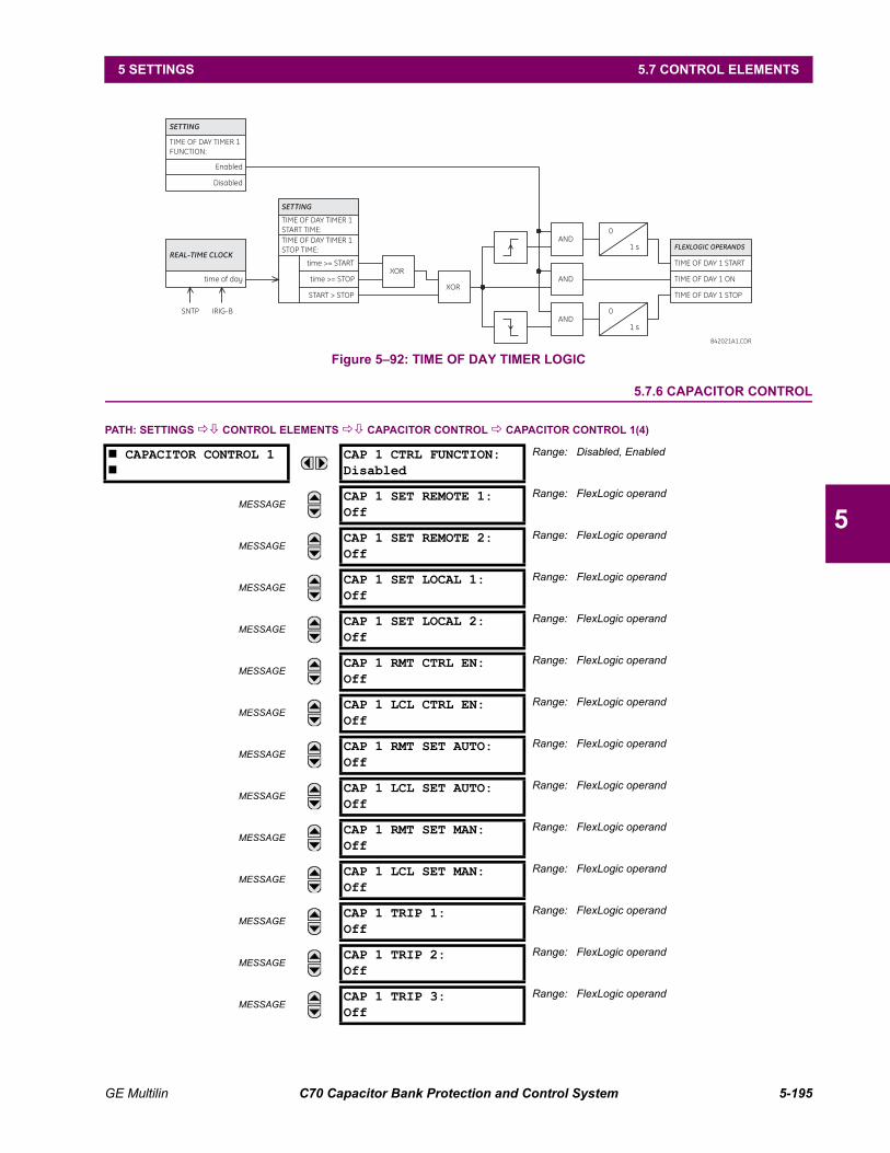
GE Multilin C70 Capacitor Bank Protection and Control System 5-195
5 SETTINGS 5.7 CONTROL ELEMENTS
5
Figure 5–92: TIME OF DAY TIMER LOGIC
5.7.6 CAPACITOR CONTROL
PATH: SETTINGS CONTROL ELEMENTS CAPACITOR CONTROL CAPACITOR CONTROL 1(4)
CAPACITOR CONTROL 1
CAP 1 CTRL FUNCTION:Disabled
Range: Disabled, Enabled
MESSAGECAP 1 SET REMOTE 1:Off
Range: FlexLogic operand
MESSAGECAP 1 SET REMOTE 2:Off
Range: FlexLogic operand
MESSAGECAP 1 SET LOCAL 1:Off
Range: FlexLogic operand
MESSAGECAP 1 SET LOCAL 2:Off
Range: FlexLogic operand
MESSAGECAP 1 RMT CTRL EN:Off
Range: FlexLogic operand
MESSAGECAP 1 LCL CTRL EN:Off
Range: FlexLogic operand
MESSAGECAP 1 RMT SET AUTO:Off
Range: FlexLogic operand
MESSAGECAP 1 LCL SET AUTO:Off
Range: FlexLogic operand
MESSAGECAP 1 RMT SET MAN:Off
Range: FlexLogic operand
MESSAGECAP 1 LCL SET MAN:Off
Range: FlexLogic operand
MESSAGECAP 1 TRIP 1:Off
Range: FlexLogic operand
MESSAGECAP 1 TRIP 2:Off
Range: FlexLogic operand
MESSAGECAP 1 TRIP 3:Off
Range: FlexLogic operand
842021A1.CDR
SETTING
TIME OF DAY TIMER 1
FUNCTION:
Enabled
Disabled
REAL-TIME CLOCK
time of day
SNTP IRIG-B
SETTING
TIME OF DAY TIMER 1
START TIME:
TIME OF DAY TIMER 1
STOP TIME:
time >= START
time >= STOP
START > STOP
XOR
XOR
AND
AND
0
1 s
0
1 s
FLEXLOGIC OPERANDS
TIME OF DAY 1 START
TIME OF DAY 1 ON
TIME OF DAY 1 STOP
AND

5-196 C70 Capacitor Bank Protection and Control System GE Multilin
5.7 CONTROL ELEMENTS 5 SETTINGS
5
MESSAGECAP 1 TRIP 4:Off
Range: FlexLogic operand
MESSAGECAP 1 TRIP 5:Off
Range: FlexLogic operand
MESSAGECAP 1 TRIP 6:Off
Range: FlexLogic operand
MESSAGECAP 1 SWITCH TOMANUAL ON TRIP: Yes
Range: Yes, No
MESSAGECAP 1 AUTO CTRL EN:Off
Range: FlexLogic operand
MESSAGECAP 1 MAN CTRL EN:Off
Range: FlexLogic operand
MESSAGECAP 1 REMOTE OPEN:Off
Range: FlexLogic operand
MESSAGECAP 1 LOCAL OPEN:Off
Range: FlexLogic operand
MESSAGECAP 1 AUTO OPEN:Off
Range: FlexLogic operand
MESSAGECAP 1 BKR OPEN 52b:Off
Range: FlexLogic operand
MESSAGECAP 1 TRIP SEAL-INDELAY: 0.400 s
Range: 0.000 to 60.000 s in steps of 0.001
MESSAGECAP 1 REMOTE CLOSE:Off
Range: FlexLogic operand
MESSAGECAP 1 LOCAL CLOSE:Off
Range: FlexLogic operand
MESSAGECAP 1 AUTO CLOSE:Off
Range: FlexLogic operand
MESSAGECAP 1 BKR CLSD 52a:Off
Range: FlexLogic operand
MESSAGECAP 1 DISCHARGEDELAY: 300 s
Range: 0 to 3600 s in steps of 1
MESSAGECAP 1 CLOSE SEAL-INDELAY: 0.400 s
Range: 0.000 to 60.000 s in steps of 0.001
MESSAGECAP 1 BKR CLOSE BLK:Off
Range: FlexLogic operand
MESSAGECAP 1 CLS OVERRIDE:Off
Range: FlexLogic operand
MESSAGECAP 1 TARGETS:Disabled
Range: Self-reset, Latched, Disabled
MESSAGECAP 1 EVENTS:Disabled
Range: Disabled, Enabled

GE Multilin C70 Capacitor Bank Protection and Control System 5-197
5 SETTINGS 5.7 CONTROL ELEMENTS
5
The capacitor control element gathers on/off commands from various sources and executes them, while maintainingremote/local and auto/manual control rights. Local control refers to control from the front panel of the relay. Remote controlrefers to control via communications from outside of the relay, an on-site interface, and/or from an off-site control center.However, there is flexibility to support other configurations.
This element provides a user-programmable time delay that inhibits closing after the bank has been switched out of serviceuntil the bank has had time to discharge any trapped charge. If the capacitor were to be closed with trapped charge ofopposite polarity from the system voltage at that instant, larger than normal transients would occur. A FlexAnalog value isavailable to inform the time remaining before the next permissible close operation.
Seal-in is provided to stretch short input commands to lengths suitable for breaker control. An interlock prevents simultane-ous trip and close output, which could result in breaker pumping. To prevent a continuous close input from causing reclos-ing of the breaker following a trip command, the interlock is sealed-in for the duration of any close input.
A provision is provided to force the auto/manual mode to manual on protection operation. This is to prevent the capacitorautomatic switching scheme from attempting to close a faulted capacitor. A setting is used to control the automatic switcho-ver to manual upon the protection trip.
The following settings are available for each capacitor control element.
• CAP 1 CTRL FUNCTION: This setting is used to enable the element. When disabled, the remote/local latch is forcedto local, the auto/manual latch is forced to manual, the trip and close command outputs are forced off, and their seal-inlatches and timers are reset.
• CAP 1 SET REMOTE 1(2): Sets one or two FlexLogic operands to select the remote mode. It is expected that one ofthese settings is programmed to a pushbutton “on” operand. This allows a local operator to hand over control to remoteoperators. Where appropriate, the other one of these settings may be set to a virtual input. This allows remote opera-tors to grant themselves control rights.
• CAP 1 SET LOCAL 1(2): Similar to previous setting, but selects local mode.
• CAP 1 RMT CTRL EN: Selects a FlexLogic operand to enables remote auto/manual and open/close control. It isexpected that this will be set to CAP 1 IN REMOTE to obtain the baseline functionality, but variations via FlexLogic arepossible. For example, should it be required that remote control is always available, this setting may be set to “On”.
• CAP 1 LCL CTRL EN: Similar to previous setting, but enables local controls. Expected to be set to CAP 1 IN LOCAL.
• CAP 1 RMT SET AUTO: Selects a FlexLogic operand that selects auto mode when remote control is enabled. It isexpected that this will be set to a virtual input to enables HMI/SCADA access via one of the supported protocols.
• CAP 1 LCL SET AUTO: Similar to previous setting, but expected to be set to a pushbutton “on” operand.
• CAP 1 RMT SET MAN: Similar to the CAP RMT SET AUTO setting, but selects manual mode.
• CAP 1 LCL SET MAN: Similar to the CAP LCL SET AUTO setting, but selects manual mode.
• CAP 1 TRIP 1(6): Selects up to six FlexLogic operands to activate the CAP 1 BKR TRIP operand, no matter what controlmodes prevail. Expected to be set to the appropriate protection element operate operand.
• CAP 1 SWITCH TO MANUAL ON TRIP: This setting allows controlling the auto/manual mode when issuing a tripcommand. If set to “Yes” the element will switch to manual mode upon tripping the bank from protection.
• CAP 1 AUTO CTRL EN: Selects a FlexLogic operand to enable automatic open/close control. It is expected that thiswill be set to CAP 1 IN AUTO to obtain the baseline functionality, but variations are possible.
• CAP 1 MAN CTRL EN: Similar to previous setting, but enables manual controls. Expected to be set to CAP 1 IN MAN.
• CAP 1 REMOTE OPEN: Selects a FlexLogic operand to activate the CAP 1 BKR TRIP operand when both remote andmanual control are enabled. It is expected that this will be set to a virtual input, and that the contact output wired to thecapacitor breaker trip coil is set to CAP 1 BKR TRIP.
• CAP 1 LOCAL OPEN: Similar to previous setting, but requires both local and manual control to be enabled. Expectedto be set to a pushbutton “on” operand.
• CAP 1 AUTO OPEN: Similar to previous setting, but requires automatic control to be enabled. Expected to be set tothe open command of the voltage regulator either built-in or customer via FlexLogic.
• CAP 1 BKR OPEN 52b: Selects a FlexLogic operand that cancels the trip seal-in. Expected to be set to the contactinput to which a contact is wired that is closed when the capacitor breaker is open. When both 52a and 52b contacts
5-198 C70 Capacitor Bank Protection and Control System GE Multilin
5.7 CONTROL ELEMENTS 5 SETTINGS
5
are used for security, the appropriate filtering logic possibly including discrepancy alarming can be programmed inFlexLogic, and the resulting virtual output can be configured under this setting.
• CAP 1 TRIP SEAL-IN DELAY: Sets a maximum trip seal-in duration for where the CAP 1 BKR OPEN 52B setting is notconfigured or fails to operate.
• CAP 1 REMOTE CLOSE: Similar to the CAP 1 REMOTE OPEN setting, but closes the breaker.
• CAP 1 LOCAL CLOSE: Similar to the CAP 1 LOCAL OPEN setting, but closes the breaker.
• CAP 1 AUTO CLOSE: Similar to the CAP 1 AUTO OPEN setting, but closes the breaker.
• CAP 1 BKR CLSD 52a: Similar to the CAP 1 BKR OPEN 52B setting, but cancels the close seal-in, and is expected to beset to a contact that is closed when the breaker is closed. The selected operand also triggers the CAP 1 DISCHARGETIME. When both 52a and 52b contacts are used for security, the appropriate filtering logic possibly including discrep-ancy alarming can be programmed in FlexLogic, and the resulting virtual output can be configured under this setting.
• CAP 1 CLOSE SEAL-IN DELAY: Sets a maximum close seal-in duration for where the CAP BKR CLOSED 52A setting isnot configured or fails to operate.
• CAP 1 DISCHARGE TIME: Sets a time delay that inhibits closing after the bank has been switched out-of-service (theCAP BKR CLOSE 52A setting goes low or trip command terminates) until the bank has had time to discharge any trappedcharge. The correct value for this setting depends on the specifics of the capacitor installation.
• CAP 1 BKR CLOSE BLK: Selects a FlexLogic operand that triggers the CAP 1 BKR CLOSE interlock logic. Its signal isexpected to originate from capacitor breaker trips external to the relay, and thus not otherwise able to block relay clos-ing (for example, from the opposite group's capacitor protection).
• CAP 1 CLS OVERRIDE: Selects a FlexLogic operand that overrides all inhibits for the breaker close command andallows the CLOSE command to be issued from any source as per the logic diagram.

GE Multilin C70 Capacitor Bank Protection and Control System 5-199
5 SETTINGS 5.7 CONTROL ELEMENTS
5
Figure 5–93: CAPACITOR BANK CONTROL SCHEME LOGIC
FLEXLOGIC OPERAND
CAP 1 IN LOCALCAP 1 IN REMOTES
R
SETTINGS
CAP 1 SET LOCAL 1
OR
OR
CAP 1 SET REMOTE 1
CAP 1 SET REMOTE 2
CAP 1 LCL CTRL EN
CAP 1 RMT CTRL EN
CAP 1 AUTO CTRL EN
CAP 1 MAN CTRL EN
AND
AND
AND
OR
OR
S
R
FLEXLOGIC OPERANDCAP 1 IN AUTOCAP 1 IN MAN
CAP 1 LCL SET AUTO
CAP 1 RMT SET AUTO
CAP 1 LCL SET MAN
CAP 1 RMT SET MAN
AND
AND
AND
ORSETTINGS
CAP 1 LOCAL OPEN
CAP 1 REMOTE OPEN
CAP 1 TRIP 1
CAP 1 TRIP 2
CAP 1 TRIP 3
CAP 1 TRIP 4
CAP 1 TRIP 5
CAP 1 TRIP 6
CAP 1 AUTO OPEN
SETTINGS
AND
AND
AND
AND
SETTINGS
CAP 1 LOCAL CLOSE
CAP 1 REMOTE CLOSE
CAP 1 AUTO CLOSE
CAP 1 CLOSE SEAL-IN DELAYSETTINGS
0
OR
AND
CAP 1 TRIP SEAL-IN DELAYSETTINGS
0tPKP
tPKP
SETTINGSCAP 1 BKR OPEN 52b
CAP 1 BKR CLSD 52a
AND
CAP 1 DISCHARGE TIME: SETTINGS
tDPO
0OR
OR
AND
SETTINGSCAP 1 BKR CLOSE BLK
FLEXLOGIC OPERANDCAP 1 BKR TRIP
FLEXLOGIC OPERANDCAP 1 BKR CLOSE
SETTINGSCAP 1 CTRL FUNCTIONEnabled = 1
AND
AND
Reset DominantNon-Volatile Latch
Reset DominantNon-Volatile Latch
FLEXLOGIC OPERANDCAP 1 DISCHARGING
FLEXANALOGCAP 1 DISCHRG TIME
seconds remaining tillclosing is enabled
Reset
SETTINGS
OR
CAP 1 SWITCH TO MANUALON TRIP:
ANDYes = 1
SETTINGCAP 1 1 CLS OVERRIDE:Off = 0
OR
SETTINGS
SETTINGS
SETTINGS
AND
CAP 1 SET LOCAL 2
OFF = 0
OFF = 0
OFF = 0
OFF = 0
OFF = 0
OFF = 0
OFF = 0
OFF = 0
OFF = 0
OFF = 0
OFF = 0
OFF = 0
OFF = 0
OFF = 0
OFF = 0
OFF = 0
OFF = 0
OFF = 0
OFF = 0
OFF = 0
OFF = 0
OFF = 0
OFF = 0
OFF = 0
OFF = 0
OFF = 0
OFF = 0
834740A1.DWG

5-200 C70 Capacitor Bank Protection and Control System GE Multilin
5.7 CONTROL ELEMENTS 5 SETTINGS
5
5.7.7 AUTOMATIC VOLTAGE REGULATOR
PATH: SETTINGS CONTROL ELEMENTS AUTOMATIC VOLTAGE REGULATOR AUTOMATIC VOLTAGE REGULATOR 1(3)
The automatic voltage regulator element (AVR) is intended to switch a static capacitor bank breaker close and open to reg-ulate either system voltage, load voltage, power factor, or reactive power. The following figure illustrates some possibleapplications.
AUTOMATIC VOLTAGE REGULATOR 1
AVR 1 FUNCTION:Disabled
Range: Disabled, Enabled
MESSAGEAVR 1 SOURCE:SRC 1
Range: SRC 1, SRC 2, SRC 3, SRC 4, SRC 5, SRC 6
MESSAGEAVR 1 MINIMUMVOLTAGE: 0.500 pu
Range: 0.500 to 1.500 pu in steps of 0.001
MESSAGEAVR 1 CONTROL MODE:Voltage
Range: Voltage, VAR
MESSAGEAVR 1 VOLT OPERATINGSIGNAL: V1
Range: Vab, Vbc, Vca, Vaver, V1, Vaux, Vag, Vbg, Vcg
MESSAGEAVR 1 VOLT LEVEL TOCLOSE: 0.950 pu
Range: 0.750 to 1.500 pu in steps of 0.001
MESSAGEAVR 1 VOLT LEVEL TOOPEN: 1.050 pu
Range: 0.750 to 1.500 pu in steps of 0.001
MESSAGEAVR 1 VOLT DROPCOMPENS Z: 0.00 Ω
Range: 0 to 250.00 ohms in steps of 0.01
MESSAGEAVR 1 VOLT DROPCOMPENS RCA: 75°
Range: 30 to 90° in steps of 1
MESSAGEAVR 1 VAR LEVEL TOCLOSE: 0.500 pu
Range: –1.500 to 1.500 pu in steps of 0.001
MESSAGEAVR 1 VAR LEVEL TOOPEN: -0.500 pu
Range: –1.500 to 1.500 pu in steps of 0.001
MESSAGEAVR 1 POWER FACTORLIMIT: 1.00
Range: 0.50 to 1.00 pu in steps of 0.01
MESSAGEAVR 1 VAR OPEN MODE:Minimize No. of Ops.
Range: Minimize Uptime, Minimize No. of Ops.
MESSAGEAVR 1 DELAY BEFORECLOSE: 1.000 s
Range: 0.000 to 65.353 s in steps of 0.001
MESSAGEAVR 1 DELAY BEFOREOPEN: 1.000 s
Range: 0.000 to 65.353 s in steps of 0.001
MESSAGEAVR 1 BLOCK:Off
Range: FlexLogic operand
MESSAGEAVR 1 TARGET:Self-reset
Range: Self-reset, Latched, Disabled
MESSAGEAVR 1 EVENTS:Disabled
Range: Disabled, Enabled

GE Multilin C70 Capacitor Bank Protection and Control System 5-201
5 SETTINGS 5.7 CONTROL ELEMENTS
5
Figure 5–94: APPLICATIONS OF THE CAPACITOR AUTOMATIC VOLTAGE REGULATOR FUNCTION
Up to three identical automatic voltage regulator elements are provided, allowing the relay to be used with capacitor banksdivided into sections for finer compensation steps, to provide switching speed dependant on the extent of the voltage orpower deviation, or to provide different settings depending on a user-programmable factor such as time of day.
Each element can be set to operate in either “Voltage” mode or “VAR” mode. The voltage mode can be used with relativelyshort time delay settings as a system stability aid, or with longer time delay settings to assist in the regulation of steadystate voltage. When the voltage decreases to the volts level to close setting, after the set close delay the capacitor isclosed, raising the voltage. When the voltage increases to the level to open setting, after the set open delay the capacitor isopened, lowering the voltage. The load drop compensation feature can be used to effectively sense the voltage at a loca-tion remote from the relay.
The “VAR” mode can be used to regulate the var and power factor of a load to reduce transmission and distribution costs. Ifthe capacitor deployment objective is to minimize system power losses, set the power factor limit to 1.000 to disable it andset the var open and close levels symmetrically about zero reactive power, with a difference between levels equal to thereactive power produced by the capacitor plus margin. Larger margins result in less frequent switching.
If on the other hand the deployment objective is solely to minimize power factor rate charges, set the power factor limit tothe value at which power factor penalties are incurred, typically 0.9. Set the var close level to the vars that would flowshould the power factor be at the limit when at the minimum expected kW demand. The open command characteristics canbe selected to suit whether the preference is to minimize the amount of time the capacitor is online or to minimize the num-ber of capacitor close operations. For the former preference, set the var open mode to “Minimize Uptime” and set the varopen level below the close level by an amount equal to the capacitor var rating plus margin. For the latter preference, setthe var open mode to “Minimize No. of Ops” (minimize number of operations) and set the var open level to the negative ofthe close level.
System
AVR
Load
a) System voltage regulation
System
AVR
Load
b) Load voltage regulation
feeder
impedance
System
AVR
Load
c) Load power factor regulation
System
AVR
Load
d) Load power factor regulation, alternate configuration
834731A1.CDR

5-202 C70 Capacitor Bank Protection and Control System GE Multilin
5.7 CONTROL ELEMENTS 5 SETTINGS
5
Figure 5–95: AUTOMATIC VOLTAGE REGULATOR PICKUP CHARACTERISTICS IN “VAR” MODE
Care should be taken that the settings do not result in the capacitor being continuously cycled close and open. In the volt-age mode the close voltage settings should be lower than the open voltage setting by more than the voltage changeexpected from capacitor switching, plus margin. Similarly in the “VAR” mode the close var setting should be higher than theopen var setting by more than the expected var change due to capacitor switching, plus margin. For configurations wherethe capacitor current is not included in the measured current, there could still be a measured var change due to loadswhose power factor increases with increasing voltage. In general, the larger the margin, the less often the capacitor will beswitched.
Delays should be set long enough to avoid undesired operations on transient conditions. Depending on the application, thiscould include operations for noise hits, for transient voltage depressions accompanying successful fault clearance, andshort-term voltage conditions pending automatic reclosure. Delays can also be used to time co-ordinate the switching ofmultiple capacitor banks, or sections of the same bank.
The following settings are available.
• AVR 1 SOURCE: Selects signal source of the control variables of interest. In case of voltage control applications, theselected source needs to have the appropriate voltages configured for proper operation. For example, when using pos-itive-sequence voltage as a control variable, phase voltages must be configured under the source; or when using sin-gle-phase auxiliary voltage, the auxiliary source voltage must be configured. In case of “VAR” mode and of voltagemode with voltage drop compensation, the indicated source must be configured with phase voltages and currents intothe regulated load or bus, and should include the capacitor current. If the source indicated here does not support thecontrol variable selected, the function will restrain itself from operating, and assert neither the close or open command.
• AVR 1 MINIMUM VOLTAGE: This value sets the minimum voltage for capacitor switching, to discriminate against lossof voltage. For voltage mode, this setting applies to the voltage selected for control. For “VAR” mode, this settingapplies to the positive sequence voltage.
• AVR 1 CONTROL MODE: This setting selects either voltage control for voltage regulation applications, or var controlfor power factor/reactive power regulation applications.
• AVR 1 VOLT OPERATING SIGNAL: When the control mode is voltage, this setting is used to select whether the AVRresponds to an individual phase-to-phase voltage or phase-to-ground voltage, the average of the three phase-to-phasevoltages, the positive sequence voltage, or the auxiliary RMS voltage. The ability to select the same voltage quantityas is used by other AVRs facilitates coordination with those AVRs.
• AVR 1 VOLT LEVEL TO CLOSE: In the voltage mode, this setting specifies the voltage level at or below which toissue the close command.
834732A1.CDR
Q
P
POWER FACTOR LIMIT
CLOSE PKP
OPEN PKP
0
VAR OPEN MODE: Minimize No. of Ops.
VAR LEVEL
TO CLOSE
VAR LEVEL
TO OPEN
Q
P
POWER FACTOR LIM
ITCLOSE PKP
0
OPEN PKP
VAR OPEN MODE: Minimize Uptime
minimum expected kW demand minimum expected kW demand
POWER FACTOR LIM
IT
VAR LEVEL
TO CLOSE
VAR LEVEL
TO OPEN

GE Multilin C70 Capacitor Bank Protection and Control System 5-203
5 SETTINGS 5.7 CONTROL ELEMENTS
5
• AVR 1 VOLT LEVEL TO OPEN: In the voltage mode, this setting specifies the voltage level at or above which to issuethe open command. The following figure illustrates voltage control level settings.
Figure 5–96: CLOSE AND OPEN LEVELS WHEN CONTROLLING VOLTAGE OR VARS
• AVR 1 VOLT DROP COMPENS Z: In the voltage mode, this setting allows compensating for voltage drop on the linewhen the relay measuring point is located upstream of the load. Positive-sequence line impedance is entered in sec-ondary ohms. Compensation cannot exceed 20% of the nominal phase voltage.
• AVR 1 VOLT DROP COMPENS RCA: In the voltage mode, this setting specifies the angle of the line impedance forvoltage drop calculations.
• AVR 1 VAR LEVEL TO CLOSE: In the “VAR” mode, this setting specifies level for the three-phase reactive power levelat or above which to issue the close command. The 1 pu value is the product of the nominal primary phase-to-phasevoltage, the CT primary, and . When the source current is an internal summation of two or more CT bank currents,the largest CT primary is used to define the 1 pu value for this setting.
• AVR 1 VAR LEVEL TO OPEN: In the “VAR” mode, this setting specifies level for the three-phase reactive power levelat or below which to issue the OPEN command. The 1 pu value is defined as for the VAR LEVEL TO CLOSE setting.
• AVR 1 POWER FACTOR LIMIT: In the “VAR” mode, this setting specifies the power factor below which close com-mands are allowed. Also affects open commands as shown in the above figure. If set to “1.00”, the power factor has noeffect.
• AVR 1 VAR OPEN MODE: Selects the close command characteristic, either “Minimize No. of Ops.” (minimize numberof operations) or “Minimize Uptime”, as described earlier in the Automatic voltage regulator pickup characteristics in“VAR” mode diagram.
• AVR 1 DELAY BEFORE CLOSE: This setting specifies delay before issuing the close command, and is used to coor-dinate with other regulators, or to ride through abnormal system conditions such as faults or re-close sequences.
• AVR 1 DELAY BEFORE OPEN: This setting specifies delay before issuing the open command, and is used to coordi-nate with other regulators, or to ride through abnormal system conditions such as faults or re-close sequences.
• AVR 1 BLOCK: This setting specifies a dynamic blocking condition. When blocked the element resets its output flagsand internal timers. VT fuse fail is a typical application.
834733A1.CDR
VOLTAGE
OPEN
CLOSE
VO
LT
LE
VE
L
TO
CL
OS
E
VO
LT
LE
VE
L
TO
OP
EN VARs
OPEN
CLOSE
VA
RL
EV
EL
TO
OP
EN
VA
RL
EV
EL
TO
CL
OS
E
3
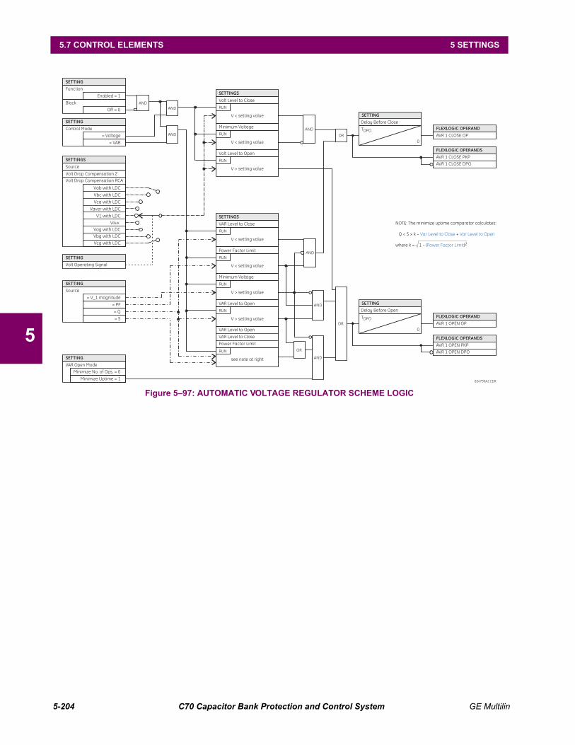
5-204 C70 Capacitor Bank Protection and Control System GE Multilin
5.7 CONTROL ELEMENTS 5 SETTINGS
5
Figure 5–97: AUTOMATIC VOLTAGE REGULATOR SCHEME LOGIC
Vbc with LDC
Vca with LDC
Vab with LDC
AND
V with LDC1
Vaux
Vaver with LDC
OR
AND
OR
AND
AND
AND
AND
AND
OR
834739A2.CDR
Vag with LDC
Vcg with LDC
Vbg with LDC
SETTING
Enabled = 1
Function
Off = 0
Block
SETTING
= Voltage
Control Mode
= VAR
SETTINGS
Volt Drop Compensation Z
Source
Volt Drop Compensation RCA
SETTING
Volt Operating Signal
SETTING
= V_1 magnitude
Source
= Q
= S
= PF
SETTINGS
Volt Level to Close
RUN
V < setting value
RUN
V < setting value
Minimum Voltage
Volt Level to Open
RUN
V > setting value
SETTINGS
VAR Level to Close
RUN
V < setting value
RUN
V < setting value
Power Factor Limit
Minimum Voltage
RUN
V > setting value
VAR Level to Open
RUN
V > setting value
VAR Level to Open
RUN
see note at right
VAR Level to Close
Power Factor Limit
SETTING
Minimize Uptime = 1
VAR Open Mode
Minimize No. of Ops. = 0
NOTE: The minimize uptime comparator calculates:
Q < S × – +
where = 1 – ( )
k
k 2
Var Level to Close Var Level to Open
Power Factor Limit
SETTING
Delay Before Close
TDPO
0
FLEXLOGIC OPERAND
AVR 1 CLOSE OP
FLEXLOGIC OPERANDS
AVR 1 CLOSE PKP
AVR 1 CLOSE DPO
SETTING
Delay Before Open
TDPO
0
FLEXLOGIC OPERAND
AVR 1 OPEN OP
FLEXLOGIC OPERANDS
AVR 1 OPEN PKP
AVR 1 OPEN DPO

GE Multilin C70 Capacitor Bank Protection and Control System 5-205
5 SETTINGS 5.7 CONTROL ELEMENTS
5
5.7.8 DIGITAL ELEMENTS
PATH: SETTINGS CONTROL ELEMENTS DIGITAL ELEMENTS DIGITAL ELEMENT 1(48)
There are 48 identical digital elements available, numbered 1 to 48. A digital element can monitor any FlexLogic operandand present a target message and/or enable events recording depending on the output operand state. The digital elementsettings include a name which will be referenced in any target message, a blocking input from any selected FlexLogic oper-and, and a timer for pickup and reset delays for the output operand.
• DIGITAL ELEMENT 1 INPUT: Selects a FlexLogic operand to be monitored by the digital element.
• DIGITAL ELEMENT 1 PICKUP DELAY: Sets the time delay to pickup. If a pickup delay is not required, set to "0".
• DIGITAL ELEMENT 1 RESET DELAY: Sets the time delay to reset. If a reset delay is not required, set to “0”.
• DIGITAL ELEMENT 1 PICKUP LED: This setting enables or disabled the digital element pickup LED. When set to“Disabled”, the operation of the pickup LED is blocked.
Figure 5–98: DIGITAL ELEMENT SCHEME LOGIC
CIRCUIT MONITORING APPLICATIONS:
Some versions of the digital input modules include an active voltage monitor circuit connected across form-A contacts. Thevoltage monitor circuit limits the trickle current through the output circuit (see technical specifications for form-A).
DIGITAL ELEMENT 1
DIGITAL ELEMENT 1FUNCTION: Disabled
Range: Disabled, Enabled
MESSAGEDIG ELEM 1 NAME:Dig Element 1
Range: 16 alphanumeric characters
MESSAGEDIG ELEM 1 INPUT:Off
Range: FlexLogic operand
MESSAGEDIG ELEM 1 PICKUPDELAY: 0.000 s
Range: 0.000 to 999999.999 s in steps of 0.001
MESSAGEDIG ELEM 1 RESETDELAY: 0.000 s
Range: 0.000 to 999999.999 s in steps of 0.001
MESSAGEDIG ELEMENT 1PICKUP LED: Enabled
Range: Disabled, Enabled
MESSAGEDIG ELEM 1 BLOCK:Off
Range: FlexLogic operand
MESSAGEDIGITAL ELEMENT 1TARGET: Self-reset
Range: Self-reset, Latched, Disabled
MESSAGEDIGITAL ELEMENT 1EVENTS: Disabled
Range: Disabled, Enabled
SETTING
DIGITAL ELEMENT 01
FUNCTION:
Disabled = 0
Enabled = 1
DIGITAL ELEMENT 01
BLOCK:
Off = 0
FLEXLOGIC OPERANDS
DIG ELEM 01 DPO
DIG ELEM 01 PKP
SETTING
827042A1.VSD
DIGITAL ELEMENT 01
INPUT:
Off = 0
SETTING
INPUT = 1
RUN tPKP
tRST
DIGITAL ELEMENT 01
PICKUP DELAY:
SETTINGS
DIGITAL ELEMENT 01
RESET DELAY:
AND
SETTING
DIGITAL ELEMENT 01
NAME:
DIG ELEM 01 OP

5-206 C70 Capacitor Bank Protection and Control System GE Multilin
5.7 CONTROL ELEMENTS 5 SETTINGS
5
As long as the current through the voltage monitor is above a threshold (see technical specifications for form-A), the “ContOp 1 VOn” FlexLogic operand will be set (for contact input 1 – corresponding operands exist for each contact output). If theoutput circuit has a high resistance or the DC current is interrupted, the trickle current will drop below the threshold and the“Cont Op 1 VOff” FlexLogic operand will be set. Consequently, the state of these operands can be used as indicators of theintegrity of the circuits in which form-A contacts are inserted.
EXAMPLE 1: BREAKER TRIP CIRCUIT INTEGRITY MONITORING
In many applications it is desired to monitor the breaker trip circuit integrity so problems can be detected before a trip oper-ation is required. The circuit is considered to be healthy when the voltage monitor connected across the trip output contactdetects a low level of current, well below the operating current of the breaker trip coil. If the circuit presents a high resis-tance, the trickle current will fall below the monitor threshold and an alarm would be declared.
In most breaker control circuits, the trip coil is connected in series with a breaker auxiliary contact which is open when thebreaker is open (see diagram below). To prevent unwanted alarms in this situation, the trip circuit monitoring logic mustinclude the breaker position.
Figure 5–99: TRIP CIRCUIT EXAMPLE 1
Assume the output contact H1 is a trip contact. Using the contact output settings, this output will be given an ID name; forexample, “Cont Op 1". Assume a 52a breaker auxiliary contact is connected to contact input H7a to monitor breaker status.Using the contact input settings, this input will be given an ID name, for example, “Cont Ip 1", and will be set “On” when thebreaker is closed. The settings to use digital element 1 to monitor the breaker trip circuit are indicated below (EnerVista URSetup example shown):
The PICKUP DELAY setting should be greater than the operating time of the breaker to avoid nuisance alarms.
NOTE

GE Multilin C70 Capacitor Bank Protection and Control System 5-207
5 SETTINGS 5.7 CONTROL ELEMENTS
5
EXAMPLE 2: BREAKER TRIP CIRCUIT INTEGRITY MONITORING
If it is required to monitor the trip circuit continuously, independent of the breaker position (open or closed), a method tomaintain the monitoring current flow through the trip circuit when the breaker is open must be provided (as shown in the fig-ure below). This can be achieved by connecting a suitable resistor (see figure below) across the auxiliary contact in the tripcircuit. In this case, it is not required to supervise the monitoring circuit with the breaker position – the BLOCK setting isselected to “Off”. In this case, the settings are as follows (EnerVista UR Setup example shown).
Figure 5–100: TRIP CIRCUIT EXAMPLE 2
The wiring connection for two examples above is applicable to both form-A contacts with voltage monitoring andsolid-state contact with voltage monitoring.
NOTE
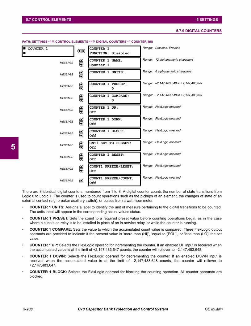
5-208 C70 Capacitor Bank Protection and Control System GE Multilin
5.7 CONTROL ELEMENTS 5 SETTINGS
5
5.7.9 DIGITAL COUNTERS
PATH: SETTINGS CONTROL ELEMENTS DIGITAL COUNTERS COUNTER 1(8)
There are 8 identical digital counters, numbered from 1 to 8. A digital counter counts the number of state transitions fromLogic 0 to Logic 1. The counter is used to count operations such as the pickups of an element, the changes of state of anexternal contact (e.g. breaker auxiliary switch), or pulses from a watt-hour meter.
• COUNTER 1 UNITS: Assigns a label to identify the unit of measure pertaining to the digital transitions to be counted.The units label will appear in the corresponding actual values status.
• COUNTER 1 PRESET: Sets the count to a required preset value before counting operations begin, as in the casewhere a substitute relay is to be installed in place of an in-service relay, or while the counter is running.
• COUNTER 1 COMPARE: Sets the value to which the accumulated count value is compared. Three FlexLogic outputoperands are provided to indicate if the present value is ‘more than (HI)’, ‘equal to (EQL)’, or ‘less than (LO)’ the setvalue.
• COUNTER 1 UP: Selects the FlexLogic operand for incrementing the counter. If an enabled UP input is received whenthe accumulated value is at the limit of +2,147,483,647 counts, the counter will rollover to –2,147,483,648.
• COUNTER 1 DOWN: Selects the FlexLogic operand for decrementing the counter. If an enabled DOWN input isreceived when the accumulated value is at the limit of –2,147,483,648 counts, the counter will rollover to+2,147,483,647.
• COUNTER 1 BLOCK: Selects the FlexLogic operand for blocking the counting operation. All counter operands areblocked.
COUNTER 1
COUNTER 1FUNCTION: Disabled
Range: Disabled, Enabled
MESSAGECOUNTER 1 NAME:Counter 1
Range: 12 alphanumeric characters
MESSAGECOUNTER 1 UNITS: Range: 6 alphanumeric characters
MESSAGECOUNTER 1 PRESET:
0
Range: –2,147,483,648 to +2,147,483,647
MESSAGECOUNTER 1 COMPARE:
0
Range: –2,147,483,648 to +2,147,483,647
MESSAGECOUNTER 1 UP:Off
Range: FlexLogic operand
MESSAGECOUNTER 1 DOWN:Off
Range: FlexLogic operand
MESSAGECOUNTER 1 BLOCK:Off
Range: FlexLogic operand
MESSAGECNT1 SET TO PRESET:Off
Range: FlexLogic operand
MESSAGECOUNTER 1 RESET:Off
Range: FlexLogic operand
MESSAGECOUNT1 FREEZE/RESET:Off
Range: FlexLogic operand
MESSAGECOUNT1 FREEZE/COUNT:Off
Range: FlexLogic operand

GE Multilin C70 Capacitor Bank Protection and Control System 5-209
5 SETTINGS 5.7 CONTROL ELEMENTS
5
• CNT1 SET TO PRESET: Selects the FlexLogic operand used to set the count to the preset value. The counter will beset to the preset value in the following situations:
1. When the counter is enabled and the CNT1 SET TO PRESET operand has the value 1 (when the counter is enabledand CNT1 SET TO PRESET operand is 0, the counter will be set to 0).
2. When the counter is running and the CNT1 SET TO PRESET operand changes the state from 0 to 1 (CNT1 SET TO
PRESET changing from 1 to 0 while the counter is running has no effect on the count).
3. When a reset or reset/freeze command is sent to the counter and the CNT1 SET TO PRESET operand has the value1 (when a reset or reset/freeze command is sent to the counter and the CNT1 SET TO PRESET operand has thevalue 0, the counter will be set to 0).
• COUNTER 1 RESET: Selects the FlexLogic operand for setting the count to either “0” or the preset value dependingon the state of the CNT1 SET TO PRESET operand.
• COUNTER 1 FREEZE/RESET: Selects the FlexLogic operand for capturing (freezing) the accumulated count valueinto a separate register with the date and time of the operation, and resetting the count to “0”.
• COUNTER 1 FREEZE/COUNT: Selects the FlexLogic operand for capturing (freezing) the accumulated count valueinto a separate register with the date and time of the operation, and continuing counting. The present accumulatedvalue and captured frozen value with the associated date/time stamp are available as actual values. If control power isinterrupted, the accumulated and frozen values are saved into non-volatile memory during the power down operation.
Figure 5–101: DIGITAL COUNTER SCHEME LOGIC
827065A1.VSD
FLEXLOGICOPERANDSCOUNTER 1 HICOUNTER 1 EQLCOUNTER 1 LO
SETTINGCOUNTER 1 FUNCTION:
Disabled = 0Enabled = 1
COUNTER 1 BLOCK:
COUNTER 1 UP:
COUNTER 1 DOWN:
COUNTER 1 RESET:
COUNT1 FREEZE/RESET:
COUNT1 FREEZE/COUNT:
Off = 0
COUNTER 1 UNITS:COUNTER 1 PRESET:
CALCULATEVALUE
RUN
SET TO PRESET VALUE
STORE DATE & TIME
COUNTER 1 NAME:
COUNTER 1 COMPARE:Count more than Comp.Count equal to Comp.Count less than Comp.
COUNTER 1 FROZEN:
Date & Time
CNT 1 SET TO PRESET:
SET TO ZERO
SETTING
SETTING
SETTING
SETTING
SETTING
SETTING
SETTING
SETTINGS
Off = 0
Off = 0
Off = 0
Off = 0
Off = 0
Off = 0
ACTUAL VALUES
COUNTER 1 ACCUM:
ACTUAL VALUE
SETTING
AND
OR
OR
AND
AND
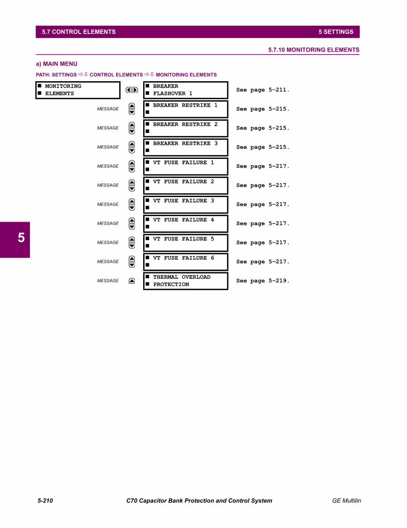
5-210 C70 Capacitor Bank Protection and Control System GE Multilin
5.7 CONTROL ELEMENTS 5 SETTINGS
5
5.7.10 MONITORING ELEMENTS
a) MAIN MENU
PATH: SETTINGS CONTROL ELEMENTS MONITORING ELEMENTS
MONITORING ELEMENTS
BREAKER FLASHOVER 1
See page 5–211.
MESSAGE BREAKER RESTRIKE 1
See page 5–215.
MESSAGE BREAKER RESTRIKE 2
See page 5–215.
MESSAGE BREAKER RESTRIKE 3
See page 5–215.
MESSAGE VT FUSE FAILURE 1
See page 5–217.
MESSAGE VT FUSE FAILURE 2
See page 5–217.
MESSAGE VT FUSE FAILURE 3
See page 5–217.
MESSAGE VT FUSE FAILURE 4
See page 5–217.
MESSAGE VT FUSE FAILURE 5
See page 5–217.
MESSAGE VT FUSE FAILURE 6
See page 5–217.
MESSAGE THERMAL OVERLOAD PROTECTION
See page 5–219.
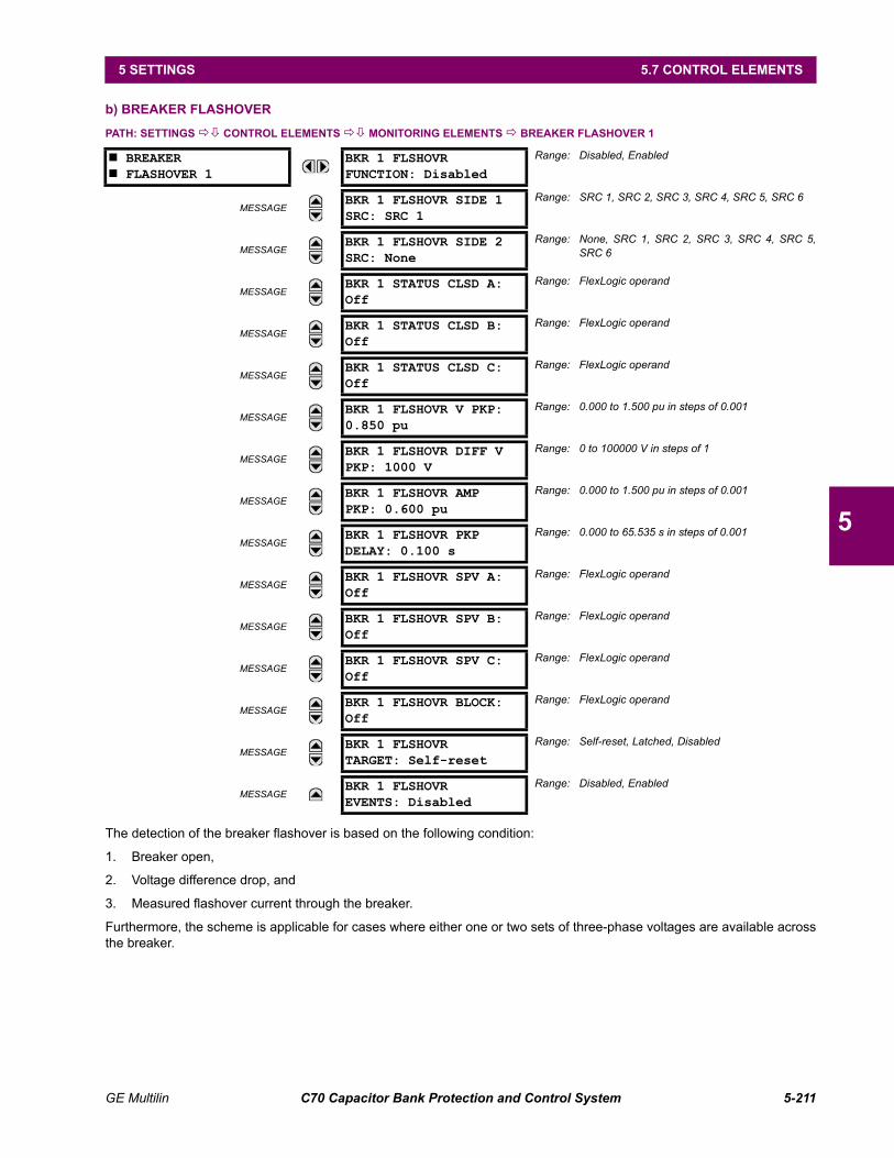
GE Multilin C70 Capacitor Bank Protection and Control System 5-211
5 SETTINGS 5.7 CONTROL ELEMENTS
5
b) BREAKER FLASHOVER
PATH: SETTINGS CONTROL ELEMENTS MONITORING ELEMENTS BREAKER FLASHOVER 1
The detection of the breaker flashover is based on the following condition:
1. Breaker open,
2. Voltage difference drop, and
3. Measured flashover current through the breaker.
Furthermore, the scheme is applicable for cases where either one or two sets of three-phase voltages are available acrossthe breaker.
BREAKER FLASHOVER 1
BKR 1 FLSHOVRFUNCTION: Disabled
Range: Disabled, Enabled
MESSAGEBKR 1 FLSHOVR SIDE 1SRC: SRC 1
Range: SRC 1, SRC 2, SRC 3, SRC 4, SRC 5, SRC 6
MESSAGEBKR 1 FLSHOVR SIDE 2SRC: None
Range: None, SRC 1, SRC 2, SRC 3, SRC 4, SRC 5,SRC 6
MESSAGEBKR 1 STATUS CLSD A:Off
Range: FlexLogic operand
MESSAGEBKR 1 STATUS CLSD B:Off
Range: FlexLogic operand
MESSAGEBKR 1 STATUS CLSD C:Off
Range: FlexLogic operand
MESSAGEBKR 1 FLSHOVR V PKP:0.850 pu
Range: 0.000 to 1.500 pu in steps of 0.001
MESSAGEBKR 1 FLSHOVR DIFF VPKP: 1000 V
Range: 0 to 100000 V in steps of 1
MESSAGEBKR 1 FLSHOVR AMPPKP: 0.600 pu
Range: 0.000 to 1.500 pu in steps of 0.001
MESSAGEBKR 1 FLSHOVR PKPDELAY: 0.100 s
Range: 0.000 to 65.535 s in steps of 0.001
MESSAGEBKR 1 FLSHOVR SPV A:Off
Range: FlexLogic operand
MESSAGEBKR 1 FLSHOVR SPV B:Off
Range: FlexLogic operand
MESSAGEBKR 1 FLSHOVR SPV C:Off
Range: FlexLogic operand
MESSAGEBKR 1 FLSHOVR BLOCK:Off
Range: FlexLogic operand
MESSAGEBKR 1 FLSHOVRTARGET: Self-reset
Range: Self-reset, Latched, Disabled
MESSAGEBKR 1 FLSHOVREVENTS: Disabled
Range: Disabled, Enabled

5-212 C70 Capacitor Bank Protection and Control System GE Multilin
5.7 CONTROL ELEMENTS 5 SETTINGS
5
Three VT Breaker Flashover Application
When only one set of VTs is available across the breaker, the BRK 1 FLSHOVR SIDE 2 SRC setting should be “None”. To detectan open breaker condition in this application, the scheme checks if the per-phase voltages were recovered (picked up), thestatus of the breaker is open (contact input indicating the breaker status is off), and no flashover current is flowing. A con-tact showing the breaker status must be provided to the relay. The voltage difference will not be considered as a conditionfor open breaker in this part of the logic.
Voltages must be present prior to flashover conditions. If the three VTs are placed after the breaker on the line (orfeeder), and the downstream breaker is open, the measured voltage would be zero and the flashover element willnot be initiated.
The flashover detection will reset if the current drops back to zero, the breaker closes, or the selected FlexLogic operandfor supervision changes to high. Using supervision through the BRK 1 FLSHOVR SPV A, BRK 1 FLSHOVR SPV B, and BRK 1
FLSHOVR SPV C settings is recommended by selecting a trip operand that will not allow the flashover element to pickup priorto the trip.
The flashover detection can be used for external alarm, re-tripping the breaker, or energizing the lockout relay.
Consider the following configuration:
The source 1 (SRC1) phase currents are feeder CTs and phase voltages are bus VTs, and Contact Input 1 is set as Breaker52a contact. The conditions prior to flashover detection are:
1. 52a status = 0.
2. VAg, VBg, or VCg is greater than the pickup setting.
3. IA, IB, IC = 0; no current flows through the breaker.
4. VA is greater than pickup (not applicable in this scheme).
The conditions at flashover detection are:
1. 52a status = 0.
2. IA, IB, or IC is greater than the pickup current flowing through the breaker.
3. VA is greater than pickup (not applicable in this scheme).
Six VT Breaker Flashover Application
The per-phase voltage difference approaches zero when the breaker is closed. The is well below any typical minimumpickup voltage. Select the level of the BRK 1 FLSHOVR DIFF V PKP setting to be less than the voltage difference measuredacross the breaker when the close or open breaker resistors are left in service. Prior to flashover, the voltage difference islarger than BRK 1 FLSHOVR DIFF V PKP. This applies to either the difference between two live voltages per phase or when thevoltage from one side of the breaker has dropped to zero (line de-energized), at least one per-phase voltage is larger thanthe BRK 1 FLSHOVR V PKP setting, and no current flows through the breaker poles. During breaker flashover, the per-phasevoltages from both sides of the breaker drops below the pickup value defined by the BRK 1 FLSHOVR V PKP setting, the volt-age difference drops below the pickup setting, and flashover current is detected. These flashover conditions initiate Flex-Logic pickup operands and start the BRK 1 FLSHOVR PKP DELAY timer.
This application does not require detection of breaker status via a 52a contact, as it uses a voltage difference larger thanthe BRK 1 FLSHOVR DIFF V PKP setting. However, monitoring the breaker contact will ensure scheme stability.
NOTE
842746A1.CDRBus VTs
Line/FeederBreakerCTs
Bus
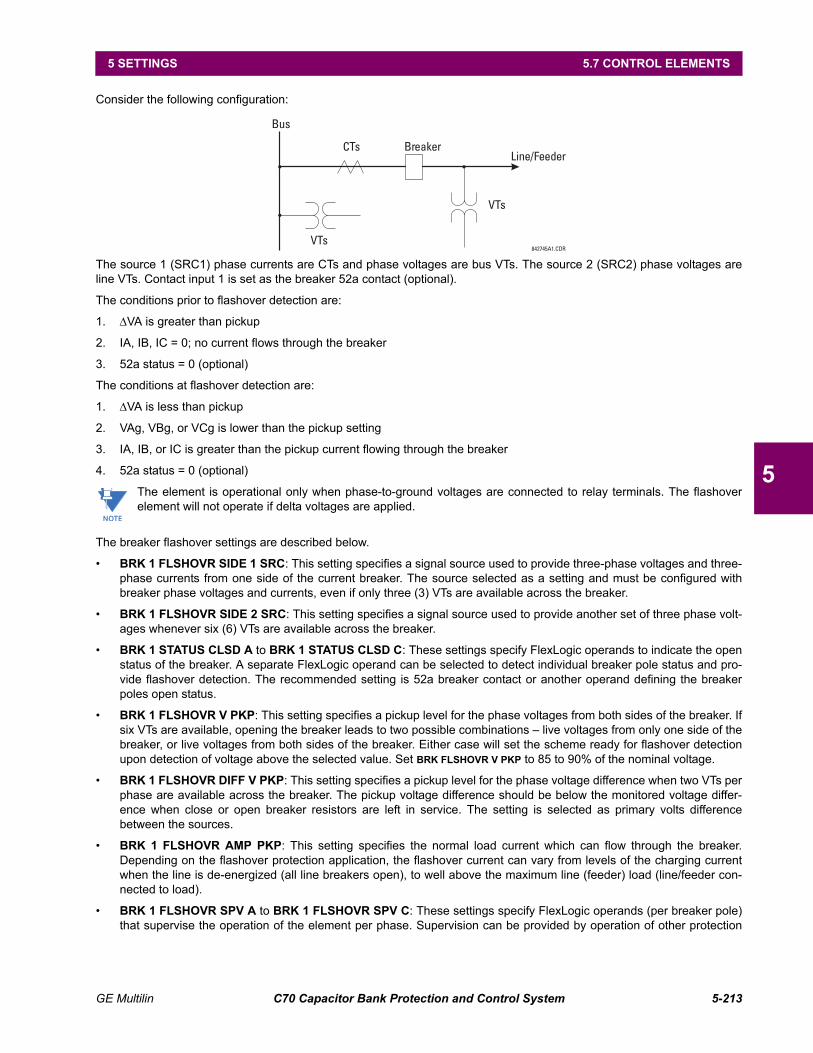
GE Multilin C70 Capacitor Bank Protection and Control System 5-213
5 SETTINGS 5.7 CONTROL ELEMENTS
5
Consider the following configuration:
The source 1 (SRC1) phase currents are CTs and phase voltages are bus VTs. The source 2 (SRC2) phase voltages areline VTs. Contact input 1 is set as the breaker 52a contact (optional).
The conditions prior to flashover detection are:
1. VA is greater than pickup
2. IA, IB, IC = 0; no current flows through the breaker
3. 52a status = 0 (optional)
The conditions at flashover detection are:
1. VA is less than pickup
2. VAg, VBg, or VCg is lower than the pickup setting
3. IA, IB, or IC is greater than the pickup current flowing through the breaker
4. 52a status = 0 (optional)
The element is operational only when phase-to-ground voltages are connected to relay terminals. The flashoverelement will not operate if delta voltages are applied.
The breaker flashover settings are described below.
• BRK 1 FLSHOVR SIDE 1 SRC: This setting specifies a signal source used to provide three-phase voltages and three-phase currents from one side of the current breaker. The source selected as a setting and must be configured withbreaker phase voltages and currents, even if only three (3) VTs are available across the breaker.
• BRK 1 FLSHOVR SIDE 2 SRC: This setting specifies a signal source used to provide another set of three phase volt-ages whenever six (6) VTs are available across the breaker.
• BRK 1 STATUS CLSD A to BRK 1 STATUS CLSD C: These settings specify FlexLogic operands to indicate the openstatus of the breaker. A separate FlexLogic operand can be selected to detect individual breaker pole status and pro-vide flashover detection. The recommended setting is 52a breaker contact or another operand defining the breakerpoles open status.
• BRK 1 FLSHOVR V PKP: This setting specifies a pickup level for the phase voltages from both sides of the breaker. Ifsix VTs are available, opening the breaker leads to two possible combinations – live voltages from only one side of thebreaker, or live voltages from both sides of the breaker. Either case will set the scheme ready for flashover detectionupon detection of voltage above the selected value. Set BRK FLSHOVR V PKP to 85 to 90% of the nominal voltage.
• BRK 1 FLSHOVR DIFF V PKP: This setting specifies a pickup level for the phase voltage difference when two VTs perphase are available across the breaker. The pickup voltage difference should be below the monitored voltage differ-ence when close or open breaker resistors are left in service. The setting is selected as primary volts differencebetween the sources.
• BRK 1 FLSHOVR AMP PKP: This setting specifies the normal load current which can flow through the breaker.Depending on the flashover protection application, the flashover current can vary from levels of the charging currentwhen the line is de-energized (all line breakers open), to well above the maximum line (feeder) load (line/feeder con-nected to load).
• BRK 1 FLSHOVR SPV A to BRK 1 FLSHOVR SPV C: These settings specify FlexLogic operands (per breaker pole)that supervise the operation of the element per phase. Supervision can be provided by operation of other protection
842745A1.CDRVTs
VTs
Line/FeederBreakerCTs
Bus
NOTE

5-214 C70 Capacitor Bank Protection and Control System GE Multilin
5.7 CONTROL ELEMENTS 5 SETTINGS
5
elements, breaker failure, and close and trip commands. A six-cycle time delay applies after the selected FlexLogicoperand resets.
• BRK FLSHOVR PKP DELAY: This setting specifies the time delay to operate after a pickup condition is detected.
Figure 5–102: BREAKER FLASHOVER SCHEME LOGIC
842018A2.CDR
AND
AND
AND
SETdominant
RESET
SETdominant
RESET
OR
OR
OR
OR
OR
BREAKER FLASHOVERFUNCTION: BRK 1 FLSHOVR V PKP:
BRK 1 STATUS CLSD A:
BRK 1 FLSHOVR PKPDELAY:
BRK 1 FLSHOVR DPO A
BRK 1 FLSHOVR PKP A
BRK 1 FLSHOVR OP
BRK 1 FLSHOVR PKP
BRK 1 FLSHOVR DPO
BRK 1 FLSHOVR OP A
BRK 1 FLSHOVR DPO B
BRK 1 FLSHOVR PKP B
BRK 1 FLSHOVR OP B
BRK 1 FLSHOVR DPO C
BRK 1 FLSHOVR PKP C
BRK 1 FLSHOVR OP C
BRK 1 FLSHOVR SUPV A:
BRK 1 STATUS CLSD B:
BRK 1 FLSHOVR SUPV B:
BRK 1 STATUS CLSD C:
BRK 1 FLSHOVR SUPV C:
BRK 1 FLSHOVR AMP PKP:
BRK 1 FLSHOVR DIFF VPKP:
BRK 1 FLSHOVR SIDE 1SRC:
BRK 1 FLSHOVR SIDE 2SRC:
Enable=1RUN
RUN
RUN
RUN
RUN
RUN
SRC 1, SRC 2, … , SRC 6
SRC 1 SRC 2 SRC 6, , … , , none
VB
Vb
IB
Block: OFF=0VA > PKP
FlexLogic operand: On=1
FlexLogic operand: Off=0
FlexLogic operand: On=1
FlexLogic operand: Off=0
Phase Blogic
Phase Blogic
Phase B logic
Phase B logic
Phase Clogic
Phase Clogic
Phase C logic
Phase C logic
FlexLogic operand: On=1
FlexLogic operand: Off=0
IA > PKP
ΔVA > PKP
Va > PKP
VA
Va
IA
VC
Vc
Δ | |VA = VA - Va
IC
SETTINGSETTING
SETTINGS
SETTING
FLEXLOGIC OPERANDS
FLEXLOGIC OPERANDS
FLEXLOGIC OPERAND
FLEXLOGIC OPERANDS
FLEXLOGIC OPERANDS
SETTINGS
SETTING
SETTING
SETTINGS
SETTINGS
0
0
5 cycle
tPKP
0
0
5 cycle
6 cycle

GE Multilin C70 Capacitor Bank Protection and Control System 5-215
5 SETTINGS 5.7 CONTROL ELEMENTS
5
c) BREAKER RESTRIKE
PATH: SETTINGS CONTROL ELEMENTS MONITORING ELEMENTS BREAKER RESTRIKE 1(3)
One breaker restrike element is provided for each CT/VT module in the C70.
According to IEEE standard C37.100: IEEE Standard Definitions for Power Switchgear, restrike is defined as “a resumptionof current between the contacts of a switching device during an opening operation after an interval of zero current of¼ cycle at normal frequency or longer”.
Figure 5–103: TYPICAL RESTRIKE WAVEFORM AND DETECTION FLAG
The breaker restrike algorithm responds to a successful interruption of the phase current following a declaration of capaci-tor bank offline as per the breaker pole indication. If a high-frequency current with a magnitude greater than the threshold isresumed at least ¼ of a cycle later than the phase current interruption, then a breaker restrike condition is declared in thecorresponding phase and the BRK RESTRIKE 1 OP operand is asserted for a short period of time. The user can add coun-ters and other logic to facilitate the decision making process as to the appropriate actions upon detecting a single restrike ora series of consecutive restrikes.
A restrike event (FlexLogic operand) is declared if all of the following hold:
BREAKER RESTRIKE 1
BREAKER RESTRIKE 1FUNCTION: Disabled
Range: Disabled, Enabled
MESSAGEBKR RSTR 1 BLOCK:Off
Range: FlexLogic operand
MESSAGEBREAKER RESTRIKE 1SOURCE: SRC 1
Range: SRC 1, SRC 2, SRC 3, SRC 4, SRC 5, SRC 6
MESSAGEBREAKER RESTRIKE 1PICKUP: 0.500 pu
Range: 0.10 to 2.00 pu in steps of 0.01
MESSAGEBREAKER RESTRIKE 1RESET DELAY: 0.100 s
Range: 0.000 to 65.535 s in steps of 0.001
MESSAGEBKR RSTR 1 BKR OPEN:Off
Range: FlexLogic operand
MESSAGEBKR RSTR 1 OPEN CMD:Off
Range: FlexLogic operand
MESSAGEBKR RSTR 1 CLS CMD:Off
Range: FlexLogic operand
MESSAGEBREAKER RESTRIKE 1TARGET: Self-reset
Range: Self-reset, Latched, Disabled
MESSAGEBREAKER RESTRIKE 1EVENTS: Disabled
Range: Disabled, Enabled
0
2
4
6
8
10
–2
–4
–6
–8
–10
0.01
0.02
0.03
0.05
time (ms)
cu
rre
nt
(am
ps)
OPERATE
834764A1.CDR

5-216 C70 Capacitor Bank Protection and Control System GE Multilin
5.7 CONTROL ELEMENTS 5 SETTINGS
5
• The current is initially interrupted.
• The breaker status is open.
• An elevated high frequency current condition occurs and the current subsequently drops out again.
The algorithm is illustrated in the state machine diagram shown below.
Figure 5–104: ALGORITHM ILLUSTRATION – STATE MACHINE TO DETECT RESTRIKE
In this way, a distinction is made between a self-extinguishing restrike and permanent breaker failure condition. The lattercan be detected by the breaker failure function or a regular instantaneous overcurrent element. Also, a fast succession ofrestrikes will be picked up by breaker failure or instantaneous overcurrent protection.
The following settings are available for each element.
• BREAKER RESTRIKE 1 FUNCTION: This setting enable and disables operation of the breaker restrike detection ele-ment.
• BRK RSTR 1 BLOCK: This setting is used to block operation of the breaker restrike detection element.
• BREAKER RESTRIKE 1 SOURCE: This setting selects the source of the current for this element. This source musthave a valid CT bank assigned.
• BREAKER RESTRIKE 1 PICKUP: This setting specifies the pickup level of the overcurrent detector in per-unit valuesof CT nominal current.
• BREAKER RESTRIKE 1 RESET DELAY: This setting specifies the reset delay for this element. When set to “0 ms”,then FlexLogic operand will be picked up for only 1/8th of the power cycle.
• BRK RSTR 1 BRK OPEN: This setting assigns a FlexLogic operand indicating the open position of the breaker. It mustbe logic “1” when breaker is open.
• BRK RSTR 1 OPEN CMD: This setting assigns a FlexLogic operand indicating a breaker open command. It must belogic “1” when breaker is opened, either manually or from protection logic.
• BRK RSTR 1 CLS CMD: This setting assigns a FlexLogic operand indicating a breaker close command. It must belogic “1” when breaker is closed.
Capacitor bank
offline
Current
interruption
(overcurrent)
High-frequency
elevated current
Restrike detected:
OP state asserted
Breaker close
Breaker
close
Breaker
close
Capacitor bank
online
Current
interruption
(overcurrent)
Breaker open
command or breaker
open state
834768A1.CDR

GE Multilin C70 Capacitor Bank Protection and Control System 5-217
5 SETTINGS 5.7 CONTROL ELEMENTS
5
Figure 5–105: BREAKER RESTRIKE SCHEME LOGIC
d) VT FUSE FAILURE
PATH: SETTINGS CONTROL ELEMENTS MONITORING ELEMENTS VT FUSE FAILURE 1(6)
Every signal source includes a fuse failure scheme.
The VT fuse failure detector can be used to raise an alarm and/or block elements that may operate incorrectly for a full orpartial loss of AC potential caused by one or more blown fuses. Some elements that might be blocked (via the BLOCK input)are distance, voltage restrained overcurrent, and directional current.
There are two classes of fuse failure that may occur:
• Class A: loss of one or two phases.
• Class B: loss of all three phases.
Different means of detection are required for each class. An indication of class A failures is a significant level of negative-sequence voltage, whereas an indication of class B failures is when positive sequence current is present and there is aninsignificant amount of positive sequence voltage. These noted indications of fuse failure could also be present when faultsare present on the system, so a means of detecting faults and inhibiting fuse failure declarations during these events is pro-vided. Once the fuse failure condition is declared, it will be sealed-in until the cause that generated it disappears.
An additional condition is introduced to inhibit a fuse failure declaration when the monitored circuit is de-energized; positive-sequence voltage and current are both below threshold levels.
The function setting enables and disables the fuse failure feature for each source.
VT FUSE FAILURE 1
VT FUSE FAILURE 1FUNCTION: Disabled
Range: Disabled, Enabled
MESSAGE NEUTRAL WIRE OPEN 1 DETECTION: Disabled
Range: Disabled, Enabled
MESSAGE NEUTRAL WIRE OPEN 1 3 HARM PKP: 0.100
0.000 to 3.000 pu in steps of 0.001
RUN
Current interruption
detection logic
< 0.05 pu
for > ¼ cycle
It
mag
ARMED
RESET
SETTING
= Enabled
BREAKER RESTRIKE 1
FUNCTION
SETTING
= Off
BKR RSTR 1 BLK
AND
SETTING
= IA
BREAKER RESTRIKE 1
SOURCE
= IB
= IC
SETTING
= Off
BKR RSTR 1 BKR OPEN
SETTING
= Off
BKR RSTR 1 OPEN CMD
SETTING
= Off
BKR RSTR 1 CLS CMD
AND
OR
SETTING
BREAKER RESTRIKE 1 PICKUP
RUN
Restrike detection logic
0
TRST
SETTING
BREAKER RESTRIKE 1
RESET DELAY
0
TRST
0
TRST
FLEXLOGIC OPERANDS
BKR RESTRIKE 1 OP A
BKR RESTRIKE 1 OP B
BKR RESTRIKE 1 OP C
BKR RESTRIKE 1 OP
FLEXLOGIC OPERAND
OR
834012A1.CDR
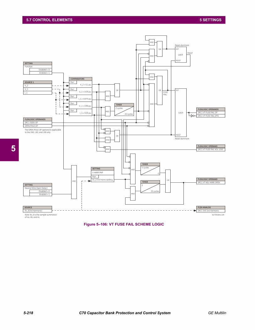
5-218 C70 Capacitor Bank Protection and Control System GE Multilin
5.7 CONTROL ELEMENTS 5 SETTINGS
5
Figure 5–106: VT FUSE FAIL SCHEME LOGIC
827093AN.CDR
FUSE
FAIL
FAULT
AND
AND
AND
AND
SET
RESET
Reset-dominant
Latch
AND
AND
AND
AND
AND
OR OR
OR
OR
Latch
SET
Reset-dominant
RESET
Function
SETTING
Disabled = 0
Enabled = 1
SOURCE 1
V_2
V_1
I_1
COMPARATORS
Run
V_1 < 0.05 pu
Run
V_2 > 0.1 pu
Run
I_1 > 0.075 pu
Run
V_1 < 0.80 pu
Run
I_1 < 0.05 pu
SRC1 50DD OP
FLEXLOGIC OPERANDS
2 cycles
20 cyclesSRC1 VT FUSE FAIL OP
FLEXLOGIC OPERANDS
SRC1 VT FUSE FAIL DPO
SRC1 VT FUSE FAIL VOL LOSS
FLEXLOGIC OPERAND
TIMER
OPEN POLE OP
The OPEN POLE OP operand is applicable
to the D60, L60, and L90 only.
Neutral Wire Open Detect
SETTING
Disabled = 0
Enabled = 1
AND
SRC1 3V0 3rd Harmonic
FLEX-ANALOG
SRC1 VT NEU WIRE OPEN
FLEXLOGIC OPERAND
3V_0(3rd Harmonic)
SOURCE
5 cycles
0
TIMER
0
20 cycles
TIMER
SETTING
Run
3V_0 3rd Harm>setting
3 HARM PKP
AND
Note 3V_0 is the sample summation
of Va, Vb, and Vc.
AND
OR

GE Multilin C70 Capacitor Bank Protection and Control System 5-219
5 SETTINGS 5.7 CONTROL ELEMENTS
5
e) THERMAL OVERLOAD PROTECTION
PATH: SETTINGS CONTROL ELEMENTS MONITORING ELEMENTS THERMAL OVERLOAD PROTECTION THERMAL
PROTECTION 1(2)
The thermal overload protection element corresponds to the IEC 255-8 standard and is used to detect thermal overloadconditions in protected power system elements. Choosing an appropriate time constant element can be used to protect dif-ferent elements of the power system. The cold curve characteristic is applied when the previous averaged load current overthe last 5 cycles is less than 10% of the base current. If this current is greater or equal than 10% than the base current, thenthe hot curve characteristic is applied.
The IEC255-8 cold curve is defined as follows:
(EQ 5.20)
The IEC255-8 hot curve is defined as follows:
(EQ 5.21)
In the above equations,
• top = time to operate.
• τop = thermal protection trip time constant.
• I = measured overload RMS current.
• Ip = measured load RMS current before overload occurs.
• k= IEC 255-8 k-factor applied to IB, defining maximum permissible current above nominal current.
• IB = protected element base (nominal) current.
THERMAL PROTECTION 1
THERMAL PROTECTION 1FUNCTION: Disabled
Range: Disabled, Enabled
MESSAGETHERMAL PROTECTION 1SOURCE: SRC1
Range: SRC 1, SRC 2, SRC 3, SRC 4, SRC 5, SRC 6
MESSAGETHERMAL PROTECTION 1BASE CURR: 0.80 pu
Range: 0.20 to 3.00 pu in steps of 0.01
MESSAGETHERMAL PROTECTION 1k FACTOR: 1.10
Range: 1.00 to 1.20 in steps of 0.05
MESSAGETHERM PROT 1 TRIPTIME CONST: 45 min.
Range: 0 to 1000 min. in steps of 1
MESSAGETHERM PROT 1 RESETTIME CONST: 45 min.
Range: 0 to 1000 min. in steps of 1
MESSAGETHERM PROT 1 MINIMRESET TIME: 20 min.
Range: 0 to 1000 min. in steps of 1
MESSAGETHERM PROT 1 RESET:Off
Range: FlexLogic operand
MESSAGETHERM PROT 1 BLOCK:Off
Range: FlexLogic operand
MESSAGETHERMAL PROTECTION 1TARGET: Self-reset
Range: Self-reset, Latched, Disabled
MESSAGETHERMAL PROTECTION 1EVENTS: Disabled
Range: Disabled, Enabled
top opI2
I2
kIB 2–--------------------------
ln=
top op
I2
Ip2
–
I2
kIB 2–--------------------------
ln=

5-220 C70 Capacitor Bank Protection and Control System GE Multilin
5.7 CONTROL ELEMENTS 5 SETTINGS
5
The reset time of the thermal overload protection element is also time delayed using following formula:
(EQ 5.22)
In the above equation,
• τrst = thermal protection trip time constant.
• Tmin is a minimum reset time setting
Figure 5–107: IEC 255-8 SAMPLE OPERATE AND RESET CURVES
The thermal overload protection element estimates accumulated thermal energy E using the following equations calculatedeach power cycle. When current is greater than the pickup level, In > k × IB, element starts increasing the thermal energy:
(EQ 5.23)
When current is less than the dropout level, In > 0.97 × k × IB, the element starts decreasing the thermal energy:
trst rst
kIB 2
I2
kIB 2–-----------------------------
ln Tmin+=
En En 1–t
top In ---------------+=

GE Multilin C70 Capacitor Bank Protection and Control System 5-221
5 SETTINGS 5.7 CONTROL ELEMENTS
5
(EQ 5.24)
In the above equations,
• Δt is the power cycle duration.
• n is the power cycle index.
• top(In) is the trip time calculated at index n as per the IEC255-8 cold curve or hot curve equations.
• trst(In) is the reset time calculated at index n as per the reset time equation.
• In is the measured overload RMS current at index n.
• En is the accumulated energy at index n.
• En – 1 is the accumulated energy at index n – 1.
The thermal overload protection element removes the THERMAL PROT 1 OP output operand when E < 0.05. In case ofemergency, the thermal memory and THERMAL PROT 1 OP output operand can be reset using THERM PROT 1 RESET setting.All calculations are performed per phase. If the accumulated energy reaches value 1 in any phase, the thermal overloadprotection element operates and only resets when energy is less than 0.05 in all three phases.
The logic for the thermal overload protection element is shown below.
Figure 5–108: THERMAL OVERLOAD PROTECTION SCHEME LOGIC
Table 5–24: TYPICAL TIME CONSTANTS
PROTECTED EQUIPMENT TIME CONSTANT MINIMUM RESET TIME
Capacitor bank 10 minutes 30 minutes
Overhead line 10 minutes 20 minutes
Air-core reactor 40 minutes 30 minutes
Busbar 60 minutes 20 minutes
Underground cable 20 to 60 minutes 60 minutes
En En 1–t
trst In ---------------–=

5-222 C70 Capacitor Bank Protection and Control System GE Multilin
5.8 INPUTS AND OUTPUTS 5 SETTINGS
5
5.8INPUTS AND OUTPUTS 5.8.1 CONTACT INPUTS
PATH: SETTINGS INPUTS/OUTPUTS CONTACT INPUTS
The contact inputs menu contains configuration settings for each contact input as well as voltage thresholds for each groupof four contact inputs. Upon startup, the relay processor determines (from an assessment of the installed modules) whichcontact inputs are available and then display settings for only those inputs.
An alphanumeric ID may be assigned to a contact input for diagnostic, setting, and event recording purposes. The CON-TACT IP X On” (Logic 1) FlexLogic operand corresponds to contact input “X” being closed, while CONTACT IP X Off corre-sponds to contact input “X” being open. The CONTACT INPUT DEBNCE TIME defines the time required for the contact toovercome ‘contact bouncing’ conditions. As this time differs for different contact types and manufacturers, set it as a maxi-mum contact debounce time (per manufacturer specifications) plus some margin to ensure proper operation. If CONTACT
INPUT EVENTS is set to “Enabled”, every change in the contact input state will trigger an event.
A raw status is scanned for all Contact Inputs synchronously at the constant rate of 0.5 ms as shown in the figure below.The DC input voltage is compared to a user-settable threshold. A new contact input state must be maintained for a user-settable debounce time in order for the C70 to validate the new contact state. In the figure below, the debounce time is setat 2.5 ms; thus the 6th sample in a row validates the change of state (mark no. 1 in the diagram). Once validated (de-bounced), the contact input asserts a corresponding FlexLogic operand and logs an event as per user setting.
A time stamp of the first sample in the sequence that validates the new state is used when logging the change of the con-tact input into the Event Recorder (mark no. 2 in the diagram).
Protection and control elements, as well as FlexLogic equations and timers, are executed eight times in a power systemcycle. The protection pass duration is controlled by the frequency tracking mechanism. The FlexLogic operand reflectingthe debounced state of the contact is updated at the protection pass following the validation (marks no. 3 and 4 on the fig-ure below). The update is performed at the beginning of the protection pass so all protection and control functions, as wellas FlexLogic equations, are fed with the updated states of the contact inputs.
CONTACT INPUTS
CONTACT INPUT H5a
MESSAGECONTACT INPUT H5a ID:Cont Ip 1
Range: up to 12 alphanumeric characters
MESSAGECONTACT INPUT H5aDEBNCE TIME: 2.0 ms
Range: 0.0 to 16.0 ms in steps of 0.5
MESSAGECONTACT INPUT H5aEVENTS: Disabled
Range: Disabled, Enabled
CONTACT INPUT xxx
CONTACT INPUT THRESHOLDS
MESSAGEIps H5a,H5c,H6a,H6cTHRESHOLD: 33 Vdc
Range: 17, 33, 84, 166 Vdc
MESSAGEIps H7a,H7c,H8a,H8cTHRESHOLD: 33 Vdc
Range: 17, 33, 84, 166 Vdc
MESSAGEIps xxx,xxx,xxx,xxxTHRESHOLD: 33 Vdc
Range: 17, 33, 84, 166 Vdc

GE Multilin C70 Capacitor Bank Protection and Control System 5-223
5 SETTINGS 5.8 INPUTS AND OUTPUTS
5
The FlexLogic operand response time to the contact input change is equal to the debounce time setting plus up to one pro-tection pass (variable and depending on system frequency if frequency tracking enabled). If the change of state occurs justafter a protection pass, the recognition is delayed until the subsequent protection pass; that is, by the entire duration of theprotection pass. If the change occurs just prior to a protection pass, the state is recognized immediately. Statistically a delayof half the protection pass is expected. Owing to the 0.5 ms scan rate, the time resolution for the input contact is below1msec.
For example, 8 protection passes per cycle on a 60 Hz system correspond to a protection pass every 2.1 ms. With a con-tact debounce time setting of 3.0 ms, the FlexLogic operand-assert time limits are: 3.0 + 0.0 = 3.0 ms and 3.0 + 2.1 = 5.1ms. These time limits depend on how soon the protection pass runs after the debouncing time.
Regardless of the contact debounce time setting, the contact input event is time-stamped with a 1 s accuracy using thetime of the first scan corresponding to the new state (mark no. 2 below). Therefore, the time stamp reflects a change in theDC voltage across the contact input terminals that was not accidental as it was subsequently validated using the debouncetimer. Keep in mind that the associated FlexLogic operand is asserted/de-asserted later, after validating the change.
The debounce algorithm is symmetrical: the same procedure and debounce time are used to filter the LOW-HIGH (marksno.1, 2, 3, and 4 in the figure below) and HIGH-LOW (marks no. 5, 6, 7, and 8 below) transitions.
Figure 5–109: INPUT CONTACT DEBOUNCING MECHANISM AND TIME-STAMPING SAMPLE TIMING
Contact inputs are isolated in groups of four to allow connection of wet contacts from different voltage sources for eachgroup. The CONTACT INPUT THRESHOLDS determine the minimum voltage required to detect a closed contact input. Thisvalue should be selected according to the following criteria: 17 for 24 V sources, 33 for 48 V sources, 84 for 110 to 125 Vsources and 166 for 250 V sources.
For example, to use contact input H5a as a status input from the breaker 52b contact to seal-in the trip relay and record it inthe Event Records menu, make the following settings changes:
CONTACT INPUT H5A ID: "Breaker Closed (52b)"CONTACT INPUT H5A EVENTS: "Enabled"
Note that the 52b contact is closed when the breaker is open and open when the breaker is closed.
842709A1.cdr
DEBOUNCE TIME
(user setting)
At this time, the
new (HIGH)
contact state is
validated
The FlexLogicTM
operand is going to
be asserted at this
protection pass
The FlexLogicTM operand
changes reflecting the
validated contact state
Time stamp of the first
scan corresponding to
the new validated state is
logged in the SOE record
2 1 3
4
DEBOUNCE TIME
(user setting)
At this time, the new
(LOW) contact state is
validated
The FlexLogicTM
operand is going to be
de-asserted at this
protection pass
The FlexLogicTM operand
changes reflecting the
validated contact state
5
7
8
Time stamp of the first
scan corresponding to the
new validated state is
logged in the SOE record
6
SCAN TIME
(0.5 msec)
PROTECTION PASS
(8 times a cycle controlled by the
frequency tracking mechanism)
RA
WC
ON
TA
CT
ST
AT
E
FLE
XLO
GIC
TM
OP
ER
AN
D
INP
UT
VO
LT
AG
E
USER-PROGRAMMABLE THRESHOLD

5-224 C70 Capacitor Bank Protection and Control System GE Multilin
5.8 INPUTS AND OUTPUTS 5 SETTINGS
5
5.8.2 VIRTUAL INPUTS
PATH: SETTINGS INPUTS/OUTPUTS VIRTUAL INPUTS VIRTUAL INPUT 1(64)
There are 64 virtual inputs that can be individually programmed to respond to input signals from the keypad (via the COM-
MANDS menu) and communications protocols. All virtual input operands are defaulted to “Off” (logic 0) unless the appropri-ate input signal is received.
If the VIRTUAL INPUT x FUNCTION is to “Disabled”, the input will be forced to off (logic 0) regardless of any attempt to alter theinput. If set to “Enabled”, the input operates as shown on the logic diagram and generates output FlexLogic operands inresponse to received input signals and the applied settings.
There are two types of operation: self-reset and latched. If VIRTUAL INPUT x TYPE is “Self-Reset”, when the input signal tran-sits from off to on, the output operand will be set to on for only one evaluation of the FlexLogic equations and then return tooff. If set to “Latched”, the virtual input sets the state of the output operand to the same state as the most recent receivedinput.
The self-reset operating mode generates the output operand for a single evaluation of the FlexLogic equations. Ifthe operand is to be used anywhere other than internally in a FlexLogic equation, it will likely have to be lengthenedin time. A FlexLogic timer with a delayed reset can perform this function.
Figure 5–110: VIRTUAL INPUTS SCHEME LOGIC
VIRTUAL INPUT 1
VIRTUAL INPUT 1FUNCTION: Disabled
Range: Disabled, Enabled
MESSAGEVIRTUAL INPUT 1 ID:Virt Ip 1
Range: Up to 12 alphanumeric characters
MESSAGEVIRTUAL INPUT 1TYPE: Latched
Range: Self-Reset, Latched
MESSAGEVIRTUAL INPUT 1EVENTS: Disabled
Range: Disabled, Enabled
NOTE
VIRTUAL INPUT 1FUNCTION:
VIRTUAL INPUT 1 ID:“Virtual Input 1 to OFF = 0”
“Virtual Input 1 to ON = 1”
AND
AND
AND
OR
SETTING
SETTING
Enabled=1
Disabled=0
(Flexlogic Operand)Virt Ip 1
827080A2.CDR
SETTING
VIRTUAL INPUT 1TYPE:
Latched
Self - Reset
R
S
Latch

GE Multilin C70 Capacitor Bank Protection and Control System 5-225
5 SETTINGS 5.8 INPUTS AND OUTPUTS
5
5.8.3 CONTACT OUTPUTS
a) DIGITAL OUTPUTS
PATH: SETTINGS INPUTS/OUTPUTS CONTACT OUTPUTS CONTACT OUTPUT H1
Upon startup of the relay, the main processor will determine from an assessment of the modules installed in the chassiswhich contact outputs are available and present the settings for only these outputs.
An ID may be assigned to each contact output. The signal that can OPERATE a contact output may be any FlexLogic oper-and (virtual output, element state, contact input, or virtual input). An additional FlexLogic operand may be used to SEAL-IN
the relay. Any change of state of a contact output can be logged as an Event if programmed to do so.
For example, the trip circuit current is monitored by providing a current threshold detector in series with some Form-A con-tacts (see the trip circuit example in the Digital elements section). The monitor will set a flag (see the specifications forForm-A). The name of the FlexLogic operand set by the monitor, consists of the output relay designation, followed by thename of the flag; for example, CONT OP 1 ION.
In most breaker control circuits, the trip coil is connected in series with a breaker auxiliary contact used to interrupt currentflow after the breaker has tripped, to prevent damage to the less robust initiating contact. This can be done by monitoringan auxiliary contact on the breaker which opens when the breaker has tripped, but this scheme is subject to incorrect oper-ation caused by differences in timing between breaker auxiliary contact change-of-state and interruption of current in thetrip circuit. The most dependable protection of the initiating contact is provided by directly measuring current in the trippingcircuit, and using this parameter to control resetting of the initiating relay. This scheme is often called trip seal-in.
This can be realized in the C70 using the CONT OP 1 ION FlexLogic operand to seal-in the contact output as follows:
CONTACT OUTPUT H1 ID: “Cont Op 1"OUTPUT H1 OPERATE: any suitable FlexLogic operandOUTPUT H1 SEAL-IN: “Cont Op 1 IOn”CONTACT OUTPUT H1 EVENTS: “Enabled”
b) LATCHING OUTPUTS
PATH: SETTINGS INPUTS/OUTPUTS CONTACT OUTPUTS CONTACT OUTPUT H1a
CONTACT OUTPUT H1
CONTACT OUTPUT H1 IDCont Op 1
Range: Up to 12 alphanumeric characters
MESSAGEOUTPUT H1 OPERATE:Off
Range: FlexLogic operand
MESSAGEOUTPUT H1 SEAL-IN:Off
Range: FlexLogic operand
MESSAGECONTACT OUTPUT H1EVENTS: Enabled
Range: Disabled, Enabled
CONTACT OUTPUT H1a
OUTPUT H1a IDL-Cont Op 1
Range: Up to 12 alphanumeric characters
MESSAGEOUTPUT H1a OPERATE:Off
Range: FlexLogic operand
MESSAGEOUTPUT H1a RESET:Off
Range: FlexLogic operand
MESSAGEOUTPUT H1a TYPE:Operate-dominant
Range: Operate-dominant, Reset-dominant
MESSAGEOUTPUT H1a EVENTS:Disabled
Range: Disabled, Enabled

5-226 C70 Capacitor Bank Protection and Control System GE Multilin
5.8 INPUTS AND OUTPUTS 5 SETTINGS
5
The C70 latching output contacts are mechanically bi-stable and controlled by two separate (open and close) coils. As suchthey retain their position even if the relay is not powered up. The relay recognizes all latching output contact cards and pop-ulates the setting menu accordingly. On power up, the relay reads positions of the latching contacts from the hardwarebefore executing any other functions of the relay (such as protection and control features or FlexLogic).
The latching output modules, either as a part of the relay or as individual modules, are shipped from the factory with alllatching contacts opened. It is highly recommended to double-check the programming and positions of the latching con-tacts when replacing a module.
Since the relay asserts the output contact and reads back its position, it is possible to incorporate self-monitoring capabili-ties for the latching outputs. If any latching outputs exhibits a discrepancy, the LATCHING OUTPUT ERROR self-test error isdeclared. The error is signaled by the LATCHING OUT ERROR FlexLogic operand, event, and target message.
• OUTPUT H1a OPERATE: This setting specifies a FlexLogic operand to operate the ‘close coil’ of the contact. Therelay will seal-in this input to safely close the contact. Once the contact is closed and the RESET input is logic 0 (off),any activity of the OPERATE input, such as subsequent chattering, will not have any effect. With both the OPERATE andRESET inputs active (logic 1), the response of the latching contact is specified by the OUTPUT H1A TYPE setting.
• OUTPUT H1a RESET: This setting specifies a FlexLogic operand to operate the ‘trip coil’ of the contact. The relay willseal-in this input to safely open the contact. Once the contact is opened and the OPERATE input is logic 0 (off), anyactivity of the RESET input, such as subsequent chattering, will not have any effect. With both the OPERATE and RESET
inputs active (logic 1), the response of the latching contact is specified by the OUTPUT H1A TYPE setting.
• OUTPUT H1a TYPE: This setting specifies the contact response under conflicting control inputs; that is, when both theOPERATE and RESET signals are applied. With both control inputs applied simultaneously, the contact will close if set to“Operate-dominant” and will open if set to “Reset-dominant”.
Application Example 1:
A latching output contact H1a is to be controlled from two user-programmable pushbuttons (buttons number 1 and 2). Thefollowing settings should be applied.
Program the Latching Outputs by making the following changes in the SETTINGS INPUTS/OUTPUTS CONTACT OUT-
PUTS CONTACT OUTPUT H1a menu (assuming an H4L module):
OUTPUT H1a OPERATE: “PUSHBUTTON 1 ON”OUTPUT H1a RESET: “PUSHBUTTON 2 ON”
Program the pushbuttons by making the following changes in the PRODUCT SETUP USER-PROGRAMMABLE PUSHBUT-
TONS USER PUSHBUTTON 1 and USER PUSHBUTTON 2 menus:
PUSHBUTTON 1 FUNCTION: “Self-reset” PUSHBUTTON 2 FUNCTION: “Self-reset”PUSHBTN 1 DROP-OUT TIME: “0.00 s” PUSHBTN 2 DROP-OUT TIME: “0.00 s”
Application Example 2:
A relay, having two latching contacts H1a and H1c, is to be programmed. The H1a contact is to be a Type-a contact, whilethe H1c contact is to be a Type-b contact (Type-a means closed after exercising the operate input; Type-b means closedafter exercising the reset input). The relay is to be controlled from virtual outputs: VO1 to operate and VO2 to reset.
Program the Latching Outputs by making the following changes in the SETTINGS INPUTS/OUTPUTS CONTACT OUT-
PUTS CONTACT OUTPUT H1a and CONTACT OUTPUT H1c menus (assuming an H4L module):
OUTPUT H1a OPERATE: “VO1” OUTPUT H1c OPERATE: “VO2”OUTPUT H1a RESET: “VO2” OUTPUT H1c RESET: “VO1”
Since the two physical contacts in this example are mechanically separated and have individual control inputs, they will notoperate at exactly the same time. A discrepancy in the range of a fraction of a maximum operating time may occur. There-fore, a pair of contacts programmed to be a multi-contact relay will not guarantee any specific sequence of operation (suchas make before break). If required, the sequence of operation must be programmed explicitly by delaying some of the con-trol inputs as shown in the next application example.
Application Example 3:
A make before break functionality must be added to the preceding example. An overlap of 20 ms is required to implementthis functionality as described below:

GE Multilin C70 Capacitor Bank Protection and Control System 5-227
5 SETTINGS 5.8 INPUTS AND OUTPUTS
5
Write the following FlexLogic equation (EnerVista UR Setup example shown):
Both timers (Timer 1 and Timer 2) should be set to 20 ms pickup and 0 ms dropout.
Program the Latching Outputs by making the following changes in the SETTINGS INPUTS/OUTPUTS CONTACT OUT-
PUTS CONTACT OUTPUT H1a and CONTACT OUTPUT H1c menus (assuming an H4L module):
OUTPUT H1a OPERATE: “VO1” OUTPUT H1c OPERATE: “VO2”OUTPUT H1a RESET: “VO4” OUTPUT H1c RESET: “VO3”
Application Example 4:
A latching contact H1a is to be controlled from a single virtual output VO1. The contact should stay closed as long as VO1is high, and should stay opened when VO1 is low. Program the relay as follows.
Write the following FlexLogic equation (EnerVista UR Setup example shown):
Program the Latching Outputs by making the following changes in the SETTINGS INPUTS/OUTPUTS CONTACT OUT-
PUTS CONTACT OUTPUT H1a menu (assuming an H4L module):
OUTPUT H1a OPERATE: “VO1”OUTPUT H1a RESET: “VO2”
5.8.4 VIRTUAL OUTPUTS
PATH: SETTINGS INPUTS/OUTPUTS VIRTUAL OUTPUTS VIRTUAL OUTPUT 1(96)
There are 96 virtual outputs that may be assigned via FlexLogic. If not assigned, the output will be forced to ‘OFF’ (Logic 0).An ID may be assigned to each virtual output. Virtual outputs are resolved in each pass through the evaluation of the Flex-Logic equations. Any change of state of a virtual output can be logged as an event if programmed to do so.
For example, if Virtual Output 1 is the trip signal from FlexLogic and the trip relay is used to signal events, the settingswould be programmed as follows:
VIRTUAL OUTPUT 1
VIRTUAL OUTPUT 1 IDVirt Op 1
Range: Up to 12 alphanumeric characters
MESSAGEVIRTUAL OUTPUT 1EVENTS: Disabled
Range: Disabled, Enabled
5-228 C70 Capacitor Bank Protection and Control System GE Multilin
5.8 INPUTS AND OUTPUTS 5 SETTINGS
5
VIRTUAL OUTPUT 1 ID: "Trip"VIRTUAL OUTPUT 1 EVENTS: "Disabled"
5.8.5 REMOTE DEVICES
a) REMOTE INPUTS/OUTPUTS OVERVIEW
Remote inputs and outputs provide a means of exchanging digital state information between Ethernet-networked devices.The IEC 61850 GSSE (Generic Substation State Event) and GOOSE (Generic Object Oriented Substation Event) stan-dards are used.
The sharing of digital point state information between GSSE/GOOSE equipped relays is essentially an extension to Flex-Logic, allowing distributed FlexLogic by making operands available to/from devices on a common communications net-work. In addition to digital point states, GSSE/GOOSE messages identify the originator of the message and provide otherinformation required by the communication specification. All devices listen to network messages and capture data only frommessages that have originated in selected devices.
IEC 61850 GSSE messages are compatible with UCA GOOSE messages and contain a fixed set of digital points. IEC61850 GOOSE messages can, in general, contain any configurable data items. When used by the remote input/output fea-ture, IEC 61850 GOOSE messages contain the same data as GSSE messages.
Both GSSE and GOOSE messages are designed to be short, reliable, and high priority. GOOSE messages have additionaladvantages over GSSE messages due to their support of VLAN (virtual LAN) and Ethernet priority tagging functionality.The GSSE message structure contains space for 128 bit pairs representing digital point state information. The IEC 61850specification provides 32 “DNA” bit pairs that represent the state of two pre-defined events and 30 user-defined events. Allremaining bit pairs are “UserSt” bit pairs, which are status bits representing user-definable events. The C70 implementationprovides 32 of the 96 available UserSt bit pairs.
The IEC 61850 specification includes features that are used to cope with the loss of communication between transmittingand receiving devices. Each transmitting device will send a GSSE/GOOSE message upon a successful power-up, whenthe state of any included point changes, or after a specified interval (the default update time) if a change-of-state has notoccurred. The transmitting device also sends a ‘hold time’ which is set greater than four times the programmed default timerequired by the receiving device.
Receiving devices are constantly monitoring the communications network for messages they require, as recognized by theidentification of the originating device carried in the message. Messages received from remote devices include the mes-sage time allowed to live. The receiving relay sets a timer assigned to the originating device to this time interval, and if ithas not received another message from this device at time-out, the remote device is declared to be non-communicating, soit will use the programmed default state for all points from that specific remote device. If a message is received from aremote device before the time allowed to live expires, all points for that device are updated to the states contained in themessage and the hold timer is restarted. The status of a remote device, where “Offline” indicates non-communicating, canbe displayed.
The remote input/output facility provides for 32 remote inputs and 64 remote outputs.
b) LOCAL DEVICES: ID OF DEVICE FOR TRANSMITTING GSSE MESSAGES
In a C70 relay, the device ID that represents the IEC 61850 GOOSE application ID (GoID) name string sent as part of eachGOOSE message is programmed in the SETTINGS PRODUCT SETUP COMMUNICATIONS IEC 61850 PROTOCOL GSSE/GOOSE CONFIGURATION TRANSMISSION FIXED GOOSE GOOSE ID setting.
Likewise, the device ID that represents the IEC 61850 GSSE application ID name string sent as part of each GSSE mes-sage is programmed in the SETTINGS PRODUCT SETUP COMMUNICATIONS IEC 61850 PROTOCOL GSSE/GOOSE
CONFIGURATION TRANSMISSION GSSE GSSE ID setting.
In C70 releases previous to 5.0x, these name strings were represented by the RELAY NAME setting.

GE Multilin C70 Capacitor Bank Protection and Control System 5-229
5 SETTINGS 5.8 INPUTS AND OUTPUTS
5
c) REMOTE DEVICES: ID OF DEVICE FOR RECEIVING GSSE/GOOSE MESSAGES
PATH: SETTINGS INPUTS/OUTPUTS REMOTE DEVICES REMOTE DEVICE 1(16)
Remote devices are available for setting purposes. A receiving relay must be programmed to capture messages from onlythose originating remote devices of interest. This setting is used to select specific remote devices by entering (bottom row)the exact identification (ID) assigned to those devices.
The REMOTE DEVICE 1 ETYPE APPID setting is only used with GOOSE messages; they are not applicable to GSSE mes-sages. This setting identifies the Ethernet application identification in the GOOSE message. It should match the corre-sponding settings on the sending device.
The REMOTE DEVICE 1 DATASET setting provides for the choice of the C70 fixed (DNA/UserSt) dataset (that is, containingDNA and UserSt bit pairs), or one of the configurable datasets.
Note that the dataset for the received data items must be made up of existing items in an existing logical node. For this rea-son, logical node GGIO3 is instantiated to hold the incoming data items. GGIO3 is not necessary to make use of thereceived data. The remote input data item mapping takes care of the mapping of the inputs to remote input FlexLogic oper-ands. However, GGIO3 data can be read by IEC 61850 clients.
5.8.6 REMOTE INPUTS
PATH: SETTINGS INPUTS/OUTPUTS REMOTE INPUTS REMOTE INPUT 1(32)
Remote Inputs that create FlexLogic operands at the receiving relay are extracted from GSSE/GOOSE messages originat-ing in remote devices. Each remote input can be selected from a list consisting of: DNA-1 through DNA-32, UserSt-1through UserSt-32, and Dataset Item 1 through Dataset Item 32. The function of DNA inputs is defined in the IEC 61850specification and is presented in the IEC 61850 DNA Assignments table in the Remote outputs section. The function ofUserSt inputs is defined by the user selection of the FlexLogic operand whose state is represented in the GSSE/GOOSEmessage. A user must program a DNA point from the appropriate FlexLogic operand.
Remote input 1 must be programmed to replicate the logic state of a specific signal from a specific remote device for localuse. This programming is performed via the three settings shown above.
The REMOTE INPUT 1 ID setting allows the user to assign descriptive text to the remote input. The REMOTE IN 1 DEVICE settingselects the remote device which originates the required signal, as previously assigned to the remote device via the settingREMOTE DEVICE (16) ID (see the Remote devices section). The REMOTE IN 1 ITEM setting selects the specific bits of theGSSE/GOOSE message required.
The REMOTE IN 1 DEFAULT STATE setting selects the logic state for this point if the local relay has just completed startup orthe remote device sending the point is declared to be non-communicating. The following choices are available:
REMOTE DEVICE 1
REMOTE DEVICE 1 ID:Remote Device 1
Range: up to 20 alphanumeric characters
MESSAGEREMOTE DEVICE 1ETYPE APPID: 0
Range: 0 to 16383 in steps of 1
MESSAGEREMOTE DEVICE 1DATASET: Fixed
Range: Fixed, GOOSE 1 through GOOSE 16
REMOTE INPUT 1
REMOTE INPUT 1 ID:Remote Ip 1
Range: up to 12 alphanumeric characters
MESSAGEREMOTE IN 1 DEVICE:Remote Device 1
Range: Remote Device 1 to Remote device 16
MESSAGEREMOTE IN 1 ITEM:None
Range: None, DNA-1 to DNA-32, UserSt-1 to UserSt-32,Config Item 1 to Config Item 32
MESSAGEREMOTE IN 1 DEFAULTSTATE: Off
Range: On, Off, Latest/On, Latest/Off
MESSAGEREMOTE IN 1EVENTS: Disabled
Range: Disabled, Enabled

5-230 C70 Capacitor Bank Protection and Control System GE Multilin
5.8 INPUTS AND OUTPUTS 5 SETTINGS
5
• Setting REMOTE IN 1 DEFAULT STATE to “On” value defaults the input to logic 1.
• Setting REMOTE IN 1 DEFAULT STATE to “Off” value defaults the input to logic 0.
• Setting REMOTE IN 1 DEFAULT STATE to “Latest/On” freezes the input in case of lost communications. If the latest state isnot known, such as after relay power-up but before the first communication exchange, the input will default to logic 1.When communication resumes, the input becomes fully operational.
• Setting REMOTE IN 1 DEFAULT STATE to “Latest/Off” freezes the input in case of lost communications. If the latest state isnot known, such as after relay power-up but before the first communication exchange, the input will default to logic 0.When communication resumes, the input becomes fully operational.
For additional information on GSSE/GOOOSE messaging, refer to the Remote Devices section in this chapter.
5.8.7 REMOTE DOUBLE-POINT STATUS INPUTS
PATH: SETTINGS INPUTS/OUTPUTS REMOTE DPS INPUTS REMOTE DPS INPUT 1(5)
Remote double-point status inputs are extracted from GOOSE messages originating in the remote device. Each remotedouble point status input must be programmed to replicate the logic state of a specific signal from a specific remote devicefor local use. This functionality is accomplished with the five remote double-point status input settings.
• REM DPS IN 1 ID: This setting assigns descriptive text to the remote double-point status input.
• REM DPS IN 1 DEV: This setting selects a remote device ID to indicate the origin of a GOOSE message. The range isselected from the remote device IDs specified in the Remote devices section.
• REM DPS IN 1 ITEM: This setting specifies the required bits of the GOOSE message.
The configurable GOOSE dataset items must be changed to accept a double-point status item from a GOOSE dataset(changes are made in the SETTINGS COMMUNICATION IEC 61850 PROTOCOL GSSE/GOOSE CONFIGURATION RECEPTION CONFIGURABLE GOOSE CONFIGURABLE GOOSE 1(16) CONFIG GSE 1 DATASET ITEMS menus). Datasetitems configured to receive any of “GGIO3.ST.IndPos1.stV” to “GGIO3.ST.IndPos5.stV” will accept double-point statusinformation that will be decoded by the remote double-point status inputs configured to this dataset item.
The remote double point status is recovered from the received IEC 61850 dataset and is available as through the RemDPSIp 1 BAD, RemDPS Ip 1 INTERM, RemDPS Ip 1 OFF, and RemDPS Ip 1 ON FlexLogic operands. These operands can then beused in breaker or disconnect control schemes.
5.8.8 REMOTE OUTPUTS
a) DNA BIT PAIRS
PATH: SETTINGS INPUTS/OUTPUTS REMOTE OUTPUTS DNA BIT PAIRS REMOTE OUTPUTS DNA- 1(32) BIT PAIR
REMOTE DPS INPUT 1
REM DPS IN 1 ID:RemDPS Ip 1
Range: up to 12 alphanumeric characters
MESSAGEREM DPS IN 1 DEV:Remote Device 1
Range: Remote Device 1 to Remote device 16
MESSAGEREM DPS IN 1 ITEM:None
Range: None, Dataset Item 1 to Dataset Item 32
MESSAGEREM DPS IN 1EVENTS: Disabled
Range: Enabled, Disabled
REMOTE OUTPUTS DNA- 1 BIT PAIR
DNA- 1 OPERAND:Off
Range: FlexLogic operand
MESSAGEDNA- 1 EVENTS:Disabled
Range: Disabled, Enabled
NOTE

GE Multilin C70 Capacitor Bank Protection and Control System 5-231
5 SETTINGS 5.8 INPUTS AND OUTPUTS
5
Remote outputs (1 to 32) are FlexLogic operands inserted into GSSE/GOOSE messages that are transmitted to remotedevices on a LAN. Each digital point in the message must be programmed to carry the state of a specific FlexLogic oper-and. The above operand setting represents a specific DNA function (as shown in the following table) to be transmitted.
b) USERST BIT PAIRS
PATH: SETTINGS INPUTS/OUTPUTS REMOTE OUTPUTS UserSt BIT PAIRS REMOTE OUTPUTS UserSt- 1(32) BIT PAIR
Remote outputs 1 to 32 originate as GSSE/GOOSE messages to be transmitted to remote devices. Each digital point in themessage must be programmed to carry the state of a specific FlexLogic operand. The setting above is used to select theoperand which represents a specific UserSt function (as selected by the user) to be transmitted.
For more information on GSSE/GOOSE messaging, refer to Remote Inputs/Outputs Overview in the RemoteDevices section.
5.8.9 RESETTING
PATH: SETTINGS INPUTS/OUTPUTS RESETTING
Some events can be programmed to latch the faceplate LED event indicators and the target message on the display. Onceset, the latching mechanism will hold all of the latched indicators or messages in the set state after the initiating conditionhas cleared until a RESET command is received to return these latches (not including FlexLogic latches) to the reset state.The RESET command can be sent from the faceplate Reset button, a remote device via a communications channel, or anyprogrammed operand.
When the RESET command is received by the relay, two FlexLogic operands are created. These operands, which arestored as events, reset the latches if the initiating condition has cleared. The three sources of RESET commands each cre-ate the RESET OP FlexLogic operand. Each individual source of a RESET command also creates its individual operandRESET OP (PUSHBUTTON), RESET OP (COMMS) or RESET OP (OPERAND) to identify the source of the command. The settingshown above selects the operand that will create the RESET OP (OPERAND) operand.
Table 5–25: IEC 61850 DNA ASSIGNMENTS
DNA IEC 61850 DEFINITION FLEXLOGIC OPERAND
1 Test IEC 61850 TEST MODE
2 ConfRev IEC 61850 CONF REV
REMOTE OUTPUTS UserSt- 1 BIT PAIR
UserSt- 1 OPERAND:Off
Range: FlexLogic operand
MESSAGEUserSt- 1 EVENTS:Disabled
Range: Disabled, Enabled
RESETTING
RESET OPERAND:Off
Range: FlexLogic operand
NOTE
5-232 C70 Capacitor Bank Protection and Control System GE Multilin
5.8 INPUTS AND OUTPUTS 5 SETTINGS
5
5.8.10 DIRECT INPUTS AND OUTPUTS
a) DIRECT INPUTS
PATH: SETTINGS INPUTS/OUTPUTS DIRECT INPUTS DIRECT INPUT 1(32)
These settings specify how the direct input information is processed. The DIRECT INPUT 1 NAME setting allows the user toassign a descriptive name to the direct input. The DIRECT INPUT 1 DEVICE ID represents the source of direct input 1. Thespecified direct input is driven by the device identified here.
The DIRECT INPUT 1 BIT NUMBER is the bit number to extract the state for direct input 1. Direct Input 1 is driven by the bitidentified as DIRECT INPUT 1 BIT NUMBER. This corresponds to the direct output number of the sending device.
The DIRECT INPUT 1 DEFAULT STATE represents the state of the direct input when the associated direct device is offline. Thefollowing choices are available:
• Setting DIRECT INPUT 1 DEFAULT STATE to “On” value defaults the input to Logic 1.
• Setting DIRECT INPUT 1 DEFAULT STATE to “Off” value defaults the input to Logic 0.
• Setting DIRECT INPUT 1 DEFAULT STATE to “Latest/On” freezes the input in case of lost communications. If the lateststate is not known, such as after relay power-up but before the first communication exchange, the input will default toLogic 1. When communication resumes, the input becomes fully operational.
• Setting DIRECT INPUT 1 DEFAULT STATE to “Latest/Off” freezes the input in case of lost communications. If the lateststate is not known, such as after relay power-up but before the first communication exchange, the input will default toLogic 0. When communication resumes, the input becomes fully operational.
b) DIRECT OUTPUTS
PATH: SETTINGS INPUTS/OUTPUTS DIRECT OUTPUTS DIRECT OUTPUT 1(32)
The DIRECT OUT 1 NAME setting allows the user to assign a descriptive name to the direct output. The DIR OUT 1 OPERAND isthe FlexLogic operand that determines the state of this direct output.
c) APPLICATION EXAMPLES
The examples introduced in the earlier Direct inputs and outputs section (part of the Product Setup section) are continuedbelow to illustrate usage of the direct inputs and outputs.
DIRECT INPUT 1
DIRECT INPUT 1NAME: Dir Ip 1
Range: up to 12 alphanumeric characters
MESSAGEDIRECT INPUT 1DEVICE ID: 1
Range: 1 to 16
MESSAGEDIRECT INPUT 1BIT NUMBER: 1
Range: 1 to 32
MESSAGEDIRECT INPUT 1DEFAULT STATE: Off
Range: On, Off, Latest/On, Latest/Off
MESSAGEDIRECT INPUT 1EVENTS: Disabled
Range: Enabled, Disabled
DIRECT OUTPUT 1
DIRECT OUT 1 NAME:Dir Out 1
Range: up to 12 alphanumeric characters
MESSAGEDIRECT OUT 1 OPERAND:Off
Range: FlexLogic operand
MESSAGEDIRECT OUTPUT 1EVENTS: Disabled
Range: Enabled, Disabled

GE Multilin C70 Capacitor Bank Protection and Control System 5-233
5 SETTINGS 5.8 INPUTS AND OUTPUTS
5
Example 1: Extending input/output capabilities of a C70 relay
Consider an application that requires additional quantities of digital inputs or output contacts or lines of programmable logicthat exceed the capabilities of a single UR-series chassis. The problem is solved by adding an extra UR-series IED, suchas the C30, to satisfy the additional inputs/outputs and programmable logic requirements. The two IEDs are connected viasingle-channel digital communication cards as shown below.
Figure 5–111: INPUT AND OUTPUT EXTENSION VIA DIRECT INPUTS AND OUTPUTS
Assume contact input 1 from UR IED 2 is to be used by UR IED 1. The following settings should be applied (Direct Input 5and bit number 12 are used, as an example):
The Cont Ip 1 On operand of UR IED 2 is now available in UR IED 1 as DIRECT INPUT 5 ON.
Example 2: Interlocking busbar protection
A simple interlocking busbar protection scheme can be accomplished by sending a blocking signal from downstreamdevices, say 2, 3 and 4, to the upstream device that monitors a single incomer of the busbar, as shown in the figure below.
Figure 5–112: SAMPLE INTERLOCKING BUSBAR PROTECTION SCHEME
Assume that Phase Instantaneous Overcurrent 1 is used by Devices 2, 3, and 4 to block Device 1. If not blocked, Device 1would trip the bus upon detecting a fault and applying a short coordination time delay.
The following settings should be applied (assume Bit 3 is used by all 3 devices to send the blocking signal and Direct Inputs7, 8, and 9 are used by the receiving device to monitor the three blocking signals):
UR IED 2: DIRECT OUT 3 OPERAND: "PHASE IOC1 OP"
UR IED 3: DIRECT OUT 3 OPERAND: "PHASE IOC1 OP"
UR IED 4: DIRECT OUT 3 OPERAND: "PHASE IOC1 OP"
UR IED 1: DIRECT INPUT 7 DEVICE ID: "2"DIRECT INPUT 7 BIT NUMBER: "3"DIRECT INPUT 7 DEFAULT STATE: select "On" for security, select "Off" for dependability
DIRECT INPUT 8 DEVICE ID: "3"DIRECT INPUT 8 BIT NUMBER: "3"DIRECT INPUT 8 DEFAULT STATE: select "On" for security, select "Off" for dependability
UR IED 1: DIRECT INPUT 5 DEVICE ID = “2”DIRECT INPUT 5 BIT NUMBER = “12”
UR IED 2: DIRECT OUT 12 OPERAND = “Cont Ip 1 On”
UR IED 1TX1
RX1
UR IED 2TX1
RX1
842712A1.CDR
UR IED 1
UR IED 2 UR IED 4UR IED 3
BLOCK

5-234 C70 Capacitor Bank Protection and Control System GE Multilin
5.8 INPUTS AND OUTPUTS 5 SETTINGS
5
DIRECT INPUT 9 DEVICE ID: "4"DIRECT INPUT 9 BIT NUMBER: "3"DIRECT INPUT 9 DEFAULT STATE: select "On" for security, select "Off" for dependability
Now the three blocking signals are available in UR IED 1 as DIRECT INPUT 7 ON, DIRECT INPUT 8 ON, and DIRECT INPUT 9ON. Upon losing communications or a device, the scheme is inclined to block (if any default state is set to “On”), or to tripthe bus on any overcurrent condition (all default states set to “Off”).
Example 2: Pilot-aided schemes
Consider a three-terminal line protection application shown in the figure below.
Figure 5–113: THREE-TERMINAL LINE APPLICATION
Assume the Hybrid Permissive Overreaching Transfer Trip (Hybrid POTT) scheme is applied using the architecture shownbelow. The scheme output operand HYB POTT TX1 is used to key the permission.
Figure 5–114: SINGLE-CHANNEL OPEN-LOOP CONFIGURATION
In the above architecture, Devices 1 and 3 do not communicate directly. Therefore, Device 2 must act as a ‘bridge’. The fol-lowing settings should be applied:
UR IED 1: DIRECT OUT 2 OPERAND: "HYB POTT TX1"DIRECT INPUT 5 DEVICE ID: "2"DIRECT INPUT 5 BIT NUMBER: "2" (this is a message from IED 2)DIRECT INPUT 6 DEVICE ID: "2"DIRECT INPUT 6 BIT NUMBER: "4" (effectively, this is a message from IED 3)
UR IED 3: DIRECT OUT 2 OPERAND: "HYB POTT TX1"DIRECT INPUT 5 DEVICE ID: "2"DIRECT INPUT 5 BIT NUMBER: "2" (this is a message from IED 2)DIRECT INPUT 6 DEVICE ID: "2"DIRECT INPUT 6 BIT NUMBER: "3" (effectively, this is a message from IED 1)
UR IED 2: DIRECT INPUT 5 DEVICE ID: "1"DIRECT INPUT 5 BIT NUMBER: "2"DIRECT INPUT 6 DEVICE ID: "3"DIRECT INPUT 6 BIT NUMBER: "2"
842713A1.CDR
UR IED 1 UR IED 2
UR IED 3
842714A1.CDR
UR IED 1TX1
RX1
UR IED 2RX2
TX2
RX1
TX1
UR IED 3RX1
TX1

GE Multilin C70 Capacitor Bank Protection and Control System 5-235
5 SETTINGS 5.8 INPUTS AND OUTPUTS
5
DIRECT OUT 2 OPERAND: "HYB POTT TX1"DIRECT OUT 3 OPERAND: "DIRECT INPUT 5" (forward a message from 1 to 3)DIRECT OUT 4 OPERAND: "DIRECT INPUT 6" (forward a message from 3 to 1)
Signal flow between the three IEDs is shown in the figure below:
Figure 5–115: SIGNAL FLOW FOR DIRECT INPUT AND OUTPUT – EXAMPLE 3
In three-terminal applications, both the remote terminals must grant permission to trip. Therefore, at each terminal, directinputs 5 and 6 should be ANDed in FlexLogic and the resulting operand configured as the permission to trip (HYB POTT RX1
setting).
5.8.11 IEC 61850 GOOSE ANALOGS
PATH: SETTINGS INPUTS/OUTPUTS IEC 61850 GOOSE ANALOGS GOOSE ANALOG INPUT 1(32)
The IEC 61850 GOOSE analog inputs feature allows the transmission of analog values between any two UR-seriesdevices. The following settings are available for each GOOSE analog input.
• ANALOG 1 DEFAULT: This setting specifies the value of the GOOSE analog input when the sending device is offlineand the ANALOG 1 DEFAULT MODE is set to “Default Value”.This setting is stored as an IEEE 754 / IEC 60559 floatingpoint number. Because of the large range of this setting, not all possible values can be stored. Some values may berounded to the closest possible floating point number.
• ANALOG 1 DEFAULT MODE: When the sending device is offline and this setting is “Last Known”, the value of theGOOSE analog input remains at the last received value. When the sending device is offline and this setting value is“Default Value”, then the value of the GOOSE analog input is defined by the ANALOG 1 DEFAULT setting.
• GOOSE ANALOG 1 UNITS: This setting specifies a four-character alphanumeric string that can is used in the actualvalues display of the corresponding GOOSE analog input value.
• GOOSE ANALOG 1 PU: This setting specifies the per-unit base factor when using the GOOSE analog input FlexAna-log values in other C70 features, such as FlexElements. The base factor is applied to the GOOSE analog input Flex-Analog quantity to normalize it to a per-unit quantity. The base units are described in the following table.
GOOSE ANALOG INPUT 1
ANALOG 1 DEFAULT:1000.000
Range: –1000000.000 to 1000000.000 in steps of 0.001
MESSAGEANALOG 1 DEFAULTMODE: Default Value
Range: Default Value, Last Known
MESSAGEGOOSE ANALOG 1UNITS:
Range: up to 4 alphanumeric characters
MESSAGEGOOSE ANALOG 1 PU:
1.000
Range: 0.000 to 1000000000.000 in steps of 0.001
842717A1.CDR
UR IED 3
UR IED 2UR IED 1
DIRECT OUT 2 = HYB POTT TX1
DIRECT INPUT 5
DIRECT INPUT 6
DIRECT OUT 2 = HYB POTT TX1
DIRECT INPUT 5
DIRECT INPUT 6
DIRECT OUT 2 = HYB POTT TX1
DIRECT INPUT 6
DIRECT OUT 4 = DIRECT INPUT 6
DIRECT OUT 3 = DIRECT INPUT 5
DIRECT INPUT 5
5-236 C70 Capacitor Bank Protection and Control System GE Multilin
5.8 INPUTS AND OUTPUTS 5 SETTINGS
5
The GOOSE analog input FlexAnalog values are available for use in other C70 functions that use FlexAnalog values.
5.8.12 IEC 61850 GOOSE INTEGERS
PATH: SETTINGS INPUTS/OUTPUTS IEC 61850 GOOSE UINTEGERS GOOSE UINTEGER INPUT 1(16)
The IEC 61850 GOOSE uinteger inputs feature allows the transmission of FlexInteger values between any two UR-seriesdevices. The following settings are available for each GOOSE uinteger input.
• UINTEGER 1 DEFAULT: This setting specifies the value of the GOOSE uinteger input when the sending device isoffline and the UINTEGER 1 DEFAULT MODE is set to “Default Value”.This setting is stored as a 32-bit unsigned integernumber.
• UINTEGER 1 DEFAULT MODE: When the sending device is offline and this setting is “Last Known”, the value of theGOOSE uinteger input remains at the last received value. When the sending device is offline and this setting value is“Default Value”, then the value of the GOOSE uinteger input is defined by the UINTEGER 1 DEFAULT setting.
The GOOSE integer input FlexInteger values are available for use in other C70 functions that use FlexInteger values.
Table 5–26: GOOSE ANALOG INPUT BASE UNITS
ELEMENT BASE UNITS
dcmA BASE = maximum value of the DCMA INPUT MAX setting for the two transducers configured under the +IN and –IN inputs.
FREQUENCY fBASE = 1 Hz
PHASE ANGLE BASE = 360 degrees (see the UR angle referencing convention)
POWER FACTOR PFBASE = 1.00
RTDs BASE = 100°C
SOURCE CURRENT IBASE = maximum nominal primary RMS value of the +IN and –IN inputs
SOURCE POWER PBASE = maximum value of VBASE IBASE for the +IN and –IN inputs
SOURCE THD & HARMONICS BASE = 1%
SOURCE VOLTAGE VBASE = maximum nominal primary RMS value of the +IN and –IN inputs
GOOSE UINTEGER INPUT 1
UINTEGER 1 DEFAULT:1000
Range: 0 to 429496295 in steps of 1
MESSAGEUINTEGER 1 DEFAULTMODE: Default Value
Range: Default Value, Last Known

GE Multilin C70 Capacitor Bank Protection and Control System 5-237
5 SETTINGS 5.9 TRANSDUCER INPUTS AND OUTPUTS
5
5.9TRANSDUCER INPUTS AND OUTPUTS 5.9.1 DCMA INPUTS
PATH: SETTINGS TRANSDUCER I/O DCMA INPUTS DCMA INPUT F1(U8)
Hardware and software is provided to receive signals from external transducers and convert these signals into a digital for-mat for use as required. The relay will accept inputs in the range of –1 to +20 mA DC, suitable for use with most commontransducer output ranges; all inputs are assumed to be linear over the complete range. Specific hardware details are con-tained in chapter 3.
Before the dcmA input signal can be used, the value of the signal measured by the relay must be converted to the rangeand quantity of the external transducer primary input parameter, such as DC voltage or temperature. The relay simplifiesthis process by internally scaling the output from the external transducer and displaying the actual primary parameter.
dcmA input channels are arranged in a manner similar to CT and VT channels. The user configures individual channelswith the settings shown here.
The channels are arranged in sub-modules of two channels, numbered from 1 through 8 from top to bottom. On power-up,the relay will automatically generate configuration settings for every channel, based on the order code, in the same generalmanner that is used for CTs and VTs. Each channel is assigned a slot letter followed by the row number, 1 through 8 inclu-sive, which is used as the channel number. The relay generates an actual value for each available input channel.
Settings are automatically generated for every channel available in the specific relay as shown above for the first channel ofa type 5F transducer module installed in slot F.
The function of the channel may be either “Enabled” or “Disabled”. If “Disabled”, no actual values are created for the chan-nel. An alphanumeric “ID” is assigned to each channel; this ID will be included in the channel actual value, along with theprogrammed units associated with the parameter measured by the transducer, such as volts, °C, megawatts, etc. This ID isalso used to reference the channel as the input parameter to features designed to measure this type of parameter. TheDCMA INPUT F1 RANGE setting specifies the mA DC range of the transducer connected to the input channel.
The DCMA INPUT F1 MIN VALUE and DCMA INPUT F1 MAX VALUE settings are used to program the span of the transducer in pri-mary units. For example, a temperature transducer might have a span from 0 to 250°C; in this case the DCMA INPUT F1 MIN
VALUE value is “0” and the DCMA INPUT F1 MAX VALUE value is “250”. Another example would be a watts transducer with aspan from –20 to +180 MW; in this case the DCMA INPUT F1 MIN VALUE value would be “–20” and the DCMA INPUT F1 MAX
VALUE value “180”. Intermediate values between the min and max values are scaled linearly.
DCMA INPUT F1
DCMA INPUT F1FUNCTION: Disabled
Range: Disabled, Enabled
MESSAGEDCMA INPUT F1 ID:DCMA Ip 1
Range: up to 20 alphanumeric characters
MESSAGEDCMA INPUT F1UNITS: A
Range: 6 alphanumeric characters
MESSAGEDCMA INPUT F1RANGE: 0 to -1 mA
Range: 0 to –1 mA, 0 to +1 mA, –1 to +1 mA, 0 to 5 mA,0 to 10mA, 0 to 20 mA, 4 to 20 mA
MESSAGEDCMA INPUT F1 MINVALUE: 0.000
Range: –9999.999 to +9999.999 in steps of 0.001
MESSAGEDCMA INPUT F1 MAXVALUE: 0.000
Range: –9999.999 to +9999.999 in steps of 0.001

5-238 C70 Capacitor Bank Protection and Control System GE Multilin
5.9 TRANSDUCER INPUTS AND OUTPUTS 5 SETTINGS
5
5.9.2 RTD INPUTS
PATH: SETTINGS TRANSDUCER I/O RTD INPUTS RTD INPUT F1(U8)
Hardware and software is provided to receive signals from external resistance temperature detectors and convert thesesignals into a digital format for use as required. These channels are intended to be connected to any of the RTD types incommon use. Specific hardware details are contained in chapter 3.
RTD input channels are arranged in a manner similar to CT and VT channels. The user configures individual channels withthe settings shown here.
The channels are arranged in sub-modules of two channels, numbered from 1 through 8 from top to bottom. On power-up,the relay will automatically generate configuration settings for every channel, based on the order code, in the same generalmanner that is used for CTs and VTs. Each channel is assigned a slot letter followed by the row number, 1 through 8 inclu-sive, which is used as the channel number. The relay generates an actual value for each available input channel.
Settings are automatically generated for every channel available in the specific relay as shown above for the first channel ofa type 5C transducer module installed in the first available slot.
The function of the channel may be either “Enabled” or “Disabled”. If “Disabled”, there will not be an actual value created forthe channel. An alphanumeric ID is assigned to the channel; this ID will be included in the channel actual values. It is alsoused to reference the channel as the input parameter to features designed to measure this type of parameter. Selecting thetype of RTD connected to the channel configures the channel.
Actions based on RTD overtemperature, such as trips or alarms, are done in conjunction with the FlexElements feature. InFlexElements, the operate level is scaled to a base of 100°C. For example, a trip level of 150°C is achieved by setting theoperate level at 1.5 pu. FlexElement operands are available to FlexLogic for further interlocking or to operate an outputcontact directly.
Refer to the following table for reference temperature values for each RTD type.
RTD INPUT F1
RTD INPUT F1FUNCTION: Disabled
Range: Disabled, Enabled
MESSAGERTD INPUT F1 ID:RTD Ip 1
Range: Up to 20 alphanumeric characters
MESSAGERTD INPUT F1 TYPE:100Ω Nickel
Range: 100Ω Nickel, 10Ω Copper, 100Ω Platinum, 120Ω Nickel
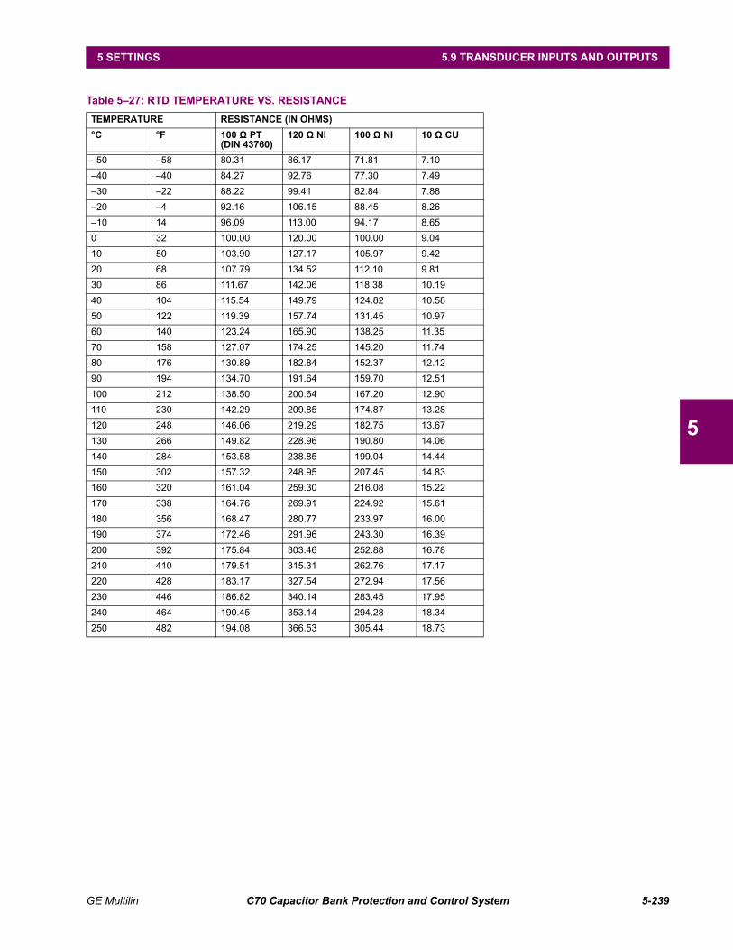
GE Multilin C70 Capacitor Bank Protection and Control System 5-239
5 SETTINGS 5.9 TRANSDUCER INPUTS AND OUTPUTS
5
Table 5–27: RTD TEMPERATURE VS. RESISTANCE
TEMPERATURE RESISTANCE (IN OHMS)
°C °F 100 Ω PT (DIN 43760)
120 Ω NI 100 Ω NI 10 Ω CU
–50 –58 80.31 86.17 71.81 7.10
–40 –40 84.27 92.76 77.30 7.49
–30 –22 88.22 99.41 82.84 7.88
–20 –4 92.16 106.15 88.45 8.26
–10 14 96.09 113.00 94.17 8.65
0 32 100.00 120.00 100.00 9.04
10 50 103.90 127.17 105.97 9.42
20 68 107.79 134.52 112.10 9.81
30 86 111.67 142.06 118.38 10.19
40 104 115.54 149.79 124.82 10.58
50 122 119.39 157.74 131.45 10.97
60 140 123.24 165.90 138.25 11.35
70 158 127.07 174.25 145.20 11.74
80 176 130.89 182.84 152.37 12.12
90 194 134.70 191.64 159.70 12.51
100 212 138.50 200.64 167.20 12.90
110 230 142.29 209.85 174.87 13.28
120 248 146.06 219.29 182.75 13.67
130 266 149.82 228.96 190.80 14.06
140 284 153.58 238.85 199.04 14.44
150 302 157.32 248.95 207.45 14.83
160 320 161.04 259.30 216.08 15.22
170 338 164.76 269.91 224.92 15.61
180 356 168.47 280.77 233.97 16.00
190 374 172.46 291.96 243.30 16.39
200 392 175.84 303.46 252.88 16.78
210 410 179.51 315.31 262.76 17.17
220 428 183.17 327.54 272.94 17.56
230 446 186.82 340.14 283.45 17.95
240 464 190.45 353.14 294.28 18.34
250 482 194.08 366.53 305.44 18.73
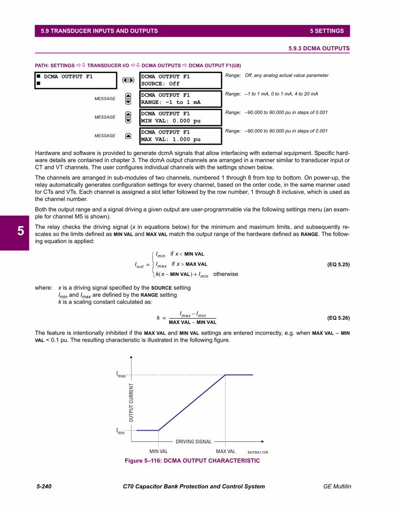
5-240 C70 Capacitor Bank Protection and Control System GE Multilin
5.9 TRANSDUCER INPUTS AND OUTPUTS 5 SETTINGS
5
5.9.3 DCMA OUTPUTS
PATH: SETTINGS TRANSDUCER I/O DCMA OUTPUTS DCMA OUTPUT F1(U8)
Hardware and software is provided to generate dcmA signals that allow interfacing with external equipment. Specific hard-ware details are contained in chapter 3. The dcmA output channels are arranged in a manner similar to transducer input orCT and VT channels. The user configures individual channels with the settings shown below.
The channels are arranged in sub-modules of two channels, numbered 1 through 8 from top to bottom. On power-up, therelay automatically generates configuration settings for every channel, based on the order code, in the same manner usedfor CTs and VTs. Each channel is assigned a slot letter followed by the row number, 1 through 8 inclusive, which is used asthe channel number.
Both the output range and a signal driving a given output are user-programmable via the following settings menu (an exam-ple for channel M5 is shown).
The relay checks the driving signal (x in equations below) for the minimum and maximum limits, and subsequently re-scales so the limits defined as MIN VAL and MAX VAL match the output range of the hardware defined as RANGE. The follow-ing equation is applied:
(EQ 5.25)
where: x is a driving signal specified by the SOURCE settingImin and Imax are defined by the RANGE settingk is a scaling constant calculated as:
(EQ 5.26)
The feature is intentionally inhibited if the MAX VAL and MIN VAL settings are entered incorrectly, e.g. when MAX VAL – MIN
VAL < 0.1 pu. The resulting characteristic is illustrated in the following figure.
Figure 5–116: DCMA OUTPUT CHARACTERISTIC
DCMA OUTPUT F1
DCMA OUTPUT F1SOURCE: Off
Range: Off, any analog actual value parameter
MESSAGEDCMA OUTPUT F1RANGE: –1 to 1 mA
Range: –1 to 1 mA, 0 to 1 mA, 4 to 20 mA
MESSAGEDCMA OUTPUT F1MIN VAL: 0.000 pu
Range: –90.000 to 90.000 pu in steps of 0.001
MESSAGEDCMA OUTPUT F1MAX VAL: 1.000 pu
Range: –90.000 to 90.000 pu in steps of 0.001
Iout
Imin if x MIN VAL
Imax if x MAX VAL
k x MIN VAL– Imin+ otherwise
=
kImax Imin–
MAX VAL MIN VAL–-------------------------------------------------=
842739A1.CDR
DRIVING SIGNAL
OU
TPU
T CU
RREN
T
MIN VAL
Imin
Imax
MAX VAL

GE Multilin C70 Capacitor Bank Protection and Control System 5-241
5 SETTINGS 5.9 TRANSDUCER INPUTS AND OUTPUTS
5
The dcmA output settings are described below.
• DCMA OUTPUT F1 SOURCE: This setting specifies an internal analog value to drive the analog output. Actual values(FlexAnalog parameters) such as power, current amplitude, voltage amplitude, power factor, etc. can be configured assources driving dcmA outputs. Refer to Appendix A for a complete list of FlexAnalog parameters.
• DCMA OUTPUT F1 RANGE: This setting allows selection of the output range. Each dcmA channel may be set inde-pendently to work with different ranges. The three most commonly used output ranges are available.
• DCMA OUTPUT F1 MIN VAL: This setting allows setting the minimum limit for the signal that drives the output. Thissetting is used to control the mapping between an internal analog value and the output current. The setting is enteredin per-unit values. The base units are defined in the same manner as the FlexElement base units.
• DCMA OUTPUT F1 MAX VAL: This setting allows setting the maximum limit for the signal that drives the output. Thissetting is used to control the mapping between an internal analog value and the output current. The setting is enteredin per-unit values. The base units are defined in the same manner as the FlexElement base units.
The DCMA OUTPUT F1 MIN VAL and DCMA OUTPUT F1 MAX VAL settings are ignored for power factor base units (i.e. ifthe DCMA OUTPUT F1 SOURCE is set to FlexAnalog value based on power factor measurement).
Three application examples are described below.
Example: power monitoring
A three phase active power on a 13.8 kV system measured via UR-series relay source 1 is to be monitored by the dcmA H1output of the range of –1 to 1 mA. The following settings are applied on the relay: CT ratio = 1200:5, VT secondary 115, VTconnection is delta, and VT ratio = 120. The nominal current is 800 A primary and the nominal power factor is 0.90. Thepower is to be monitored in both importing and exporting directions and allow for 20% overload compared to the nominal.
The nominal three-phase power is:
(EQ 5.27)
The three-phase power with 20% overload margin is:
(EQ 5.28)
The base unit for power (refer to the FlexElements section in this chapter for additional details) is:
(EQ 5.29)
The minimum and maximum power values to be monitored (in pu) are:
(EQ 5.30)
The following settings should be entered:
DCMA OUTPUT H1 SOURCE: “SRC 1 P”DCMA OUTPUT H1 RANGE: “–1 to 1 mA”DCMA OUTPUT H1 MIN VAL: “–1.247 pu”DCMA OUTPUT H1 MAX VAL: “1.247 pu”
With the above settings, the output will represent the power with the scale of 1 mA per 20.65 MW. The worst-case error forthis application can be calculated by superimposing the following two sources of error:
• ±0.5% of the full scale for the analog output module, or
• ±1% of reading error for the active power at power factor of 0.9
For example at the reading of 20 MW, the worst-case error is 0.01 20 MW + 0.207 MW = 0.407 MW.
Example: current monitoring
The phase A current (true RMS value) is to be monitored via the H2 current output working with the range from 4 to 20 mA.The CT ratio is 5000:5 and the maximum load current is 4200 A. The current should be monitored from 0 A upwards, allow-ing for 50% overload.
The phase current with the 50% overload margin is:
NOTE
P 3 13.8 kV 0.8 kA 0.9 17.21 MW= =
Pmax 1.2 17.21 MW 20.65 MW= =
PBASE 115 V 120 1.2 kA 16.56 MW= =
minimum power 20.65 MW–16.56 MW------------------------------ 1.247 pu, maximum power 20.65 MW
16.56 MW--------------------------- 1.247 pu= =–= =
0.005 1 1– – 20.65 MW 0.207 MW=

5-242 C70 Capacitor Bank Protection and Control System GE Multilin
5.9 TRANSDUCER INPUTS AND OUTPUTS 5 SETTINGS
5
(EQ 5.31)
The base unit for current (refer to the FlexElements section in this chapter for additional details) is:
(EQ 5.32)
The minimum and maximum power values to be monitored (in pu) are:
(EQ 5.33)
The following settings should be entered:
DCMA OUTPUT H2 SOURCE: “SRC 1 Ia RMS”DCMA OUTPUT H2 RANGE: “4 to 20 mA”DCMA OUTPUT H2 MIN VAL: “0.000 pu”DCMA OUTPUT H2 MAX VAL: “1.260 pu”
The worst-case error for this application could be calculated by superimposing the following two sources of error:
• ±0.5% of the full scale for the analog output module, or
• ±0.25% of reading or ±0.1% of rated (whichever is greater) for currents between 0.1 and 2.0 of nominal
For example, at the reading of 4.2 kA, the worst-case error is max(0.0025 4.2 kA, 0.001 5 kA) + 0.504 kA = 0.515 kA.
Example: voltage monitoring
A positive-sequence voltage on a 400 kV system measured via source 2 is to be monitored by the dcmA H3 output with arange of 0 to 1 mA. The VT secondary setting is 66.4 V, the VT ratio setting is 6024, and the VT connection setting is“Delta”. The voltage should be monitored in the range from 70% to 110% of nominal.
The minimum and maximum positive-sequence voltages to be monitored are:
(EQ 5.34)
The base unit for voltage (refer to the FlexElements section in this chapter for additional details) is:
(EQ 5.35)
The minimum and maximum voltage values to be monitored (in pu) are:
(EQ 5.36)
The following settings should be entered:
DCMA OUTPUT H3 SOURCE: “SRC 2 V_1 mag”DCMA OUTPUT H3 RANGE: “0 to 1 mA”DCMA OUTPUT H3 MIN VAL: “0.404 pu”DCMA OUTPUT H3 MAX VAL: “0.635 pu”
The limit settings differ from the expected 0.7 pu and 1.1 pu because the relay calculates the positive-sequence quantitiesscaled to the phase-to-ground voltages, even if the VTs are connected in “Delta” (refer to the Metering conventions sectionin chapter 6), while at the same time the VT nominal voltage is 1 pu for the settings. Consequently the settings required inthis example differ from naturally expected by the factor of .
The worst-case error for this application could be calculated by superimposing the following two sources of error:
• ±0.5% of the full scale for the analog output module, or
• ±0.5% of reading
For example, under nominal conditions, the positive-sequence reads 230.94 kV and the worst-case error is0.005 x 230.94 kV + 1.27 kV = 2.42 kV.
Imax 1.5 4.2 kA 6.3 kA= =
IBASE 5 kA=
minimum current 0 kA5 kA------------ 0 pu, maximum current 6.3 kA
5 kA----------------- 1.26 pu= == =
0.005 20 4– 6.3 kA 0.504 kA=
Vmin 0.7400 kV
3------------------- 161.66 kV, Vmax 1.1
400 kV
3------------------- 254.03 kV= == =
VBASE 0.0664 kV 6024 400 kV= =
minimum voltage 161.66 kV400 kV--------------------------- 0.404 pu, maximum voltage 254.03 kV
400 kV--------------------------- 0.635 pu= == =
3
0.005 1 0– 254.03 kV 1.27 kV=

GE Multilin C70 Capacitor Bank Protection and Control System 5-243
5 SETTINGS 5.10 TESTING
5
5.10TESTING 5.10.1 TEST MODE
PATH: SETTINGS TESTING TEST MODE
The C70 provides a test facility to verify the functionality of contact inputs and outputs, some communication channels andthe phasor measurement unit (where applicable), using simulated conditions. The test mode is indicated on the relay face-plate by a Test Mode LED indicator.
The test mode may be in any of three states: disabled, isolated, or forcible.
In the “Disabled” mode, C70 operation is normal and all test features are disabled.
In the “Isolated” mode, the C70 is prevented from performing certain control actions, including tripping via contact outputs.All relay contact outputs, including latching outputs, are disabled. Channel tests and phasor measurement unit tests remainusable on applicable UR-series models.
In the “Forcible” mode, the operand selected by the TEST MODE FORCING setting controls the relay inputs and outputs. If thetest mode is forcible, and the operand assigned to the TEST MODE FORCING setting is “Off”, the C70 inputs and outputs oper-ate normally. If the test mode is forcible, and the operand assigned to the TEST MODE FORCING setting is “On”, the C70 con-tact inputs and outputs are forced to the values specified in the following sections. Forcing may be controlled by manuallychanging the operand selected by the TEST MODE FORCING setting between on and off, or by selecting a user-programma-ble pushbutton, contact input, or communication-based input operand. Channel tests and phasor measurement unit testsremain usable on applicable UR-series models.
Communications based inputs and outputs remain fully operational in test mode. If a control action is programmedusing direct inputs and outputs or remote inputs and outputs, then the test procedure must take this into account.
When in “Forcible” mode, the operand selected by the TEST MODE FORCING setting dictates further response of the C70 totesting conditions. To force contact inputs and outputs through relay settings, set TEST MODE FORCING to “On”. To force con-tact inputs and outputs through a user-programmable condition, such as FlexLogic operand (pushbutton, digital input, com-munication-based input, or a combination of these), set TEST MODE FORCING to the desired operand. The contact input oroutput is forced when the selected operand assumes a logic 1 state.
The C70 remains fully operational in test mode, allowing for various testing procedures. In particular, the protection andcontrol elements, FlexLogic, and communication-based inputs and outputs function normally.
The only difference between the normal operation and the test mode is the behavior of the input and output contacts. Thecontact inputs can be forced to report as open or closed or remain fully operational, whereas the contact outputs can beforced to open, close, freeze, or remain fully operational. The response of the digital input and output contacts to the testmode is programmed individually for each input and output using the force contact inputs and force contact outputs testfunctions described in the following sections.
The test mode state is indicated on the relay faceplate by a combination of the Test Mode LED indicator, the In-Service LEDindicator, and by the critical fail relay, as shown in the following table.
SETTINGS TESTING
TEST MODEFUNCTION: Disabled
Range: Disabled, Isolated, Forcible
MESSAGETEST MODE FORCING:On
Range: FlexLogic operand
NOTE

5-244 C70 Capacitor Bank Protection and Control System GE Multilin
5.10 TESTING 5 SETTINGS
5
The TEST MODE FUNCTION setting can only be changed by a direct user command. Following a restart, power up, settingsupload, or firmware upgrade, the test mode will remain at the last programmed value. This allows a C70 that has beenplaced in isolated mode to remain isolated during testing and maintenance activities. On restart, the TEST MODE FORCING
setting and the force contact input and force contact output settings all revert to their default states.
5.10.2 FORCE CONTACT INPUTS
PATH: SETTINGS TESTING FORCE CONTACT INPUTS
The relay digital inputs (contact inputs) could be pre-programmed to respond to the test mode in the following ways:
• If set to “Disabled”, the input remains fully operational. It is controlled by the voltage across its input terminals and canbe turned on and off by external circuitry. This value should be selected if a given input must be operational during thetest. This includes, for example, an input initiating the test, or being a part of a user pre-programmed test sequence.
• If set to “Open”, the input is forced to report as opened (Logic 0) for the entire duration of the test mode regardless ofthe voltage across the input terminals.
• If set to “Closed”, the input is forced to report as closed (Logic 1) for the entire duration of the test mode regardless ofthe voltage across the input terminals.
The force contact inputs feature provides a method of performing checks on the function of all contact inputs. Onceenabled, the relay is placed into test mode, allowing this feature to override the normal function of contact inputs. The TestMode LED will be on, indicating that the relay is in test mode. The state of each contact input may be programmed as “Dis-abled”, “Open”, or “Closed”. All contact input operations return to normal when all settings for this feature are disabled.
Table 5–28: TEST MODE OPERATION
TEST MODE FUNCTION
TEST MODE FORCING OPERAND
IN-SERVICE LED
TEST MODE LED
CRITICAL FAIL RELAY
INPUT AND OUTPUT BEHAVIOR
Disabled No effect Unaffected Off Unaffected Contact outputs and inputs are under normal operation. Channel tests and PMU tests not operational (where applicable).
Isolated No effect Off On De-energized
Contact outputs are disabled and contact inputs are operational. Channel tests and PMU tests are also operational (where applicable).
Forcible On (logic 1) Off Flashing De-energized
Contact inputs and outputs are controlled by the force contact input and force contact output functions. Channel tests and PMU tests are operational (where applicable).
Off (logic 0) Off Flashing De-energized
Contact outputs and inputs are under normal operation. Channel tests and PMU tests are also operational (where applicable).
FORCE CONTACT INPUTS
FORCE Cont Ip 1:Disabled
Range: Disabled, Open, Closed
MESSAGEFORCE Cont Ip 2:Disabled
Range: Disabled, Open, Closed
MESSAGEFORCE Cont Ip xx:Disabled
Range: Disabled, Open, Closed

GE Multilin C70 Capacitor Bank Protection and Control System 5-245
5 SETTINGS 5.10 TESTING
5
5.10.3 FORCE CONTACT OUTPUTS
PATH: SETTINGS TESTING FORCE CONTACT OUTPUTS
The relay contact outputs can be pre-programmed to respond to the test mode.
If set to “Disabled”, the contact output remains fully operational. If operates when its control operand is logic 1 and willresets when its control operand is logic 0. If set to “Energized”, the output will close and remain closed for the entire dura-tion of the test mode, regardless of the status of the operand configured to control the output contact. If set to “De-ener-gized”, the output will open and remain opened for the entire duration of the test mode regardless of the status of theoperand configured to control the output contact. If set to “Freeze”, the output retains its position from before entering thetest mode, regardless of the status of the operand configured to control the output contact.
These settings are applied two ways. First, external circuits may be tested by energizing or de-energizing contacts. Sec-ond, by controlling the output contact state, relay logic may be tested and undesirable effects on external circuits avoided.
Example 1: Initiating test mode through user-programmable pushbutton 1
For example, the test mode can be initiated from user-programmable pushbutton 1. The pushbutton will be programmed as“Latched” (pushbutton pressed to initiate the test, and pressed again to terminate the test). During the test, digital input 1should remain operational, digital inputs 2 and 3 should open, and digital input 4 should close. Also, contact output 1 shouldfreeze, contact output 2 should open, contact output 3 should close, and contact output 4 should remain fully operational.The required settings are shown below.
To enable user-programmable pushbutton 1 to initiate the test mode, make the following changes in the SETTINGS TESTING TEST MODE menu: TEST MODE FUNCTION: “Enabled” and TEST MODE INITIATE: “PUSHBUTTON 1 ON”
Make the following changes to configure the contact inputs and outputs. In the SETTINGS TESTING FORCE CONTACT
INPUTS and FORCE CONTACT OUTPUTS menus, set:
FORCE Cont Ip 1: “Disabled”, FORCE Cont Ip 2: “Open”, FORCE Cont Ip 3: “Open”, and FORCE Cont Ip 4: “Closed”FORCE Cont Op 1: “Freeze”, FORCE Cont Op 2: “De-energized”, FORCE Cont Op 3: “Energized”,
and FORCE Cont Op 4: “Disabled”
Example 2: Initiating a test from user-programmable pushbutton 1 or through remote input 1
In this example, the test can be initiated locally from user-programmable pushbutton 1 or remotely through remote input 1.Both the pushbutton and the remote input will be programmed as “Latched”. Write the following FlexLogic equation:
Set the user-programmable pushbutton as latching by changing SETTINGS PRODUCT SETUP USER-PROGRAMMABLE
PUSHBUTTONS USER PUSHBUTTON 1 PUSHBUTTON 1 FUNCTION to “Latched”. To enable either pushbutton 1 or remoteinput 1 to initiate the Test mode, make the following changes in the SETTINGS TESTING TEST MODE menu:
TEST MODE FUNCTION: “Enabled” and TEST MODE INITIATE: “VO1”
FORCE CONTACT OUTPUTS
FORCE Cont Op 1:Disabled
Range: Disabled, Energized, De-energized, Freeze
MESSAGEFORCE Cont Op 2:Disabled
Range: Disabled, Energized, De-energized, Freeze
MESSAGEFORCE Cont Op xx:Disabled
Range: Disabled, Energized, De-energized, Freeze

5-246 C70 Capacitor Bank Protection and Control System GE Multilin
5.10 TESTING 5 SETTINGS
5

GE Multilin C70 Capacitor Bank Protection and Control System 6-1
6 ACTUAL VALUES 6.1 OVERVIEW
6
6 ACTUAL VALUES 6.1OVERVIEW 6.1.1 ACTUAL VALUES MENU
ACTUAL VALUES STATUS
CONTACT INPUTS
See page 6-3.
VIRTUAL INPUTS
See page 6-3.
REMOTE INPUTS
See page 6-3.
REMOTE DPS INPUTS
See page 6-4.
CONTACT OUTPUTS
See page 6-4.
VIRTUAL OUTPUTS
See page 6-4.
REMOTE DEVICES STATUS
See page 6-5.
REMOTE DEVICES STATISTICS
See page 6-5.
DIGITAL COUNTERS
See page 6-5.
SELECTOR SWITCHES
See page 6-6.
TIME OF DAY TIMERS
See page 6-6.
FLEX STATES
See page 6-6.
ETHERNET
See page 6-6.
REAL TIME CLOCK SYNCHRONIZING
See page 6-7.
DIRECT INPUTS
See page 6-8.
DIRECT DEVICES STATUS
See page 6-8.
IEC 61850 GOOSE UINTEGERS
See page 6-9.
COMM STATUS REMAINING CONNECT See page 6-9.
ACTUAL VALUES METERING
SOURCE SRC 1
See page 6-13.
SOURCE SRC 2

6-2 C70 Capacitor Bank Protection and Control System GE Multilin
6.1 OVERVIEW 6 ACTUAL VALUES
6
SOURCE SRC 3
SOURCE SRC 4
SOURCE SRC 5
SOURCE SRC 6
CAPACITOR CONTROL
See page 6-17.
CAPACITOR BANK
See page 6-18.
TRACKING FREQUENCY
See page 6-19.
FLEXELEMENTS
See page 6-19.
IEC 61850 GOOSE ANALOGS
See page 6-20.
TRANSDUCER I/O DCMA INPUTS
See page 6-20.
TRANSDUCER I/O RTD INPUTS
See page 6-20.
ACTUAL VALUES RECORDS
USER-PROGRAMMABLE FAULT REPORT
See page 6-21.
EVENT RECORDS
See page 6-21.
OSCILLOGRAPHY
See page 6-21.
DATA LOGGER
See page 6-22.
ACTUAL VALUES PRODUCT INFO
MODEL INFORMATION
See page 6-23.
FIRMWARE REVISIONS
See page 6-23.
GE Multilin C70 Capacitor Bank Protection and Control System 6-3
6 ACTUAL VALUES 6.2 STATUS
6
6.2STATUS
For status reporting, ‘On’ represents Logic 1 and ‘Off’ represents Logic 0.
6.2.1 CONTACT INPUTS
PATH: ACTUAL VALUES STATUS CONTACT INPUTS
The present status of the contact inputs is shown here. The first line of a message display indicates the ID of the contactinput. For example, ‘Cont Ip 1’ refers to the contact input in terms of the default name-array index. The second line of thedisplay indicates the logic state of the contact input.
6.2.2 VIRTUAL INPUTS
PATH: ACTUAL VALUES STATUS VIRTUAL INPUTS
The present status of the 64 virtual inputs is shown here. The first line of a message display indicates the ID of the virtualinput. For example, ‘Virt Ip 1’ refers to the virtual input in terms of the default name. The second line of the display indicatesthe logic state of the virtual input.
6.2.3 REMOTE INPUTS
PATH: ACTUAL VALUES STATUS REMOTE INPUTS
The present state of the 32 remote inputs is shown here.
The state displayed will be that of the remote point unless the remote device has been established to be “Offline” in whichcase the value shown is the programmed default state for the remote input.
CONTACT INPUTS
Cont Ip 1Off
Range: On, Off
MESSAGECont Ip 2Off
Range: On, Off
MESSAGECont Ip xxOff
Range: On, Off
VIRTUAL INPUTS
Virt Ip 1Off
Range: On, Off
MESSAGEVirt Ip 2Off
Range: On, Off
MESSAGEVirt Ip 64Off
Range: On, Off
REMOTE INPUTS
REMOTE INPUT 1STATUS: Off
Range: On, Off
MESSAGEREMOTE INPUT 2STATUS: Off
Range: On, Off
MESSAGEREMOTE INPUT 32STATUS: Off
Range: On, Off
NOTE

6-4 C70 Capacitor Bank Protection and Control System GE Multilin
6.2 STATUS 6 ACTUAL VALUES
6
6.2.4 REMOTE DOUBLE-POINT STATUS INPUTS
PATH: ACTUAL VALUES STATUS REMOTE DPS INPUTS
The present state of the remote double-point status inputs is shown here. The actual values indicate if the remote double-point status inputs are in the on (close), off (open), intermediate, or bad state.
6.2.5 CONTACT OUTPUTS
PATH: ACTUAL VALUES STATUS CONTACT OUTPUTS
The present state of the contact outputs is shown here. The first line of a message display indicates the ID of the contactoutput. For example, ‘Cont Op 1’ refers to the contact output in terms of the default name-array index. The second line ofthe display indicates the logic state of the contact output.
For form-A contact outputs, the state of the voltage and current detectors is displayed as Off, VOff, IOff, On, IOn,and VOn. For form-C contact outputs, the state is displayed as Off or On.
6.2.6 VIRTUAL OUTPUTS
PATH: ACTUAL VALUES STATUS VIRTUAL OUTPUTS
The present state of up to 96 virtual outputs is shown here. The first line of a message display indicates the ID of the virtualoutput. For example, ‘Virt Op 1’ refers to the virtual output in terms of the default name-array index. The second line of thedisplay indicates the logic state of the virtual output, as calculated by the FlexLogic equation for that output.
REMOTE DPS INPUTS
REMOTE DPS INPUT 1STATUS: Bad
Range: On, Off, Intermediate, Bad
MESSAGEREMOTE DPS INPUT 2STATUS: Bad
Range: On, Off, Intermediate, Bad
MESSAGEREMOTE DPS INPUT 5STATUS: Bad
Range: On, Off, Intermediate, Bad
CONTACT OUTPUTS
Cont Op 1Off
Range: On, Off, VOff, VOn, IOn, IOff
MESSAGECont Op 2Off
Range: On, Off, VOff, VOn, IOn, IOff
MESSAGECont Op xxOff
Range: On, Off, VOff, VOn, IOn, IOff
VIRTUAL OUTPUTS
Virt Op 1Off
Range: On, Off
MESSAGEVirt Op 2Off
Range: On, Off
MESSAGEVirt Op 96Off
Range: On, Off
NOTE

GE Multilin C70 Capacitor Bank Protection and Control System 6-5
6 ACTUAL VALUES 6.2 STATUS
6
6.2.7 REMOTE DEVICES
a) STATUS
PATH: ACTUAL VALUES STATUS REMOTE DEVICES STATUS
The present state of the programmed remote devices is shown here. The ALL REMOTE DEVICES ONLINE message indicateswhether or not all programmed remote devices are online. If the corresponding state is "No", then at least one requiredremote device is not online.
b) STATISTICS
PATH: ACTUAL VALUES STATUS REMOTE DEVICES STATISTICS REMOTE DEVICE 1(16)
Statistical data (two types) for up to 16 programmed remote devices is shown here.
The STNUM number is obtained from the indicated remote device and increments whenever a change of state of at leastone item occurs in the GSSE/GOOSE message. The SQNUM number is obtained from the indicated remote device andincrements whenever a GSSE/GOOSE message, without a state change, is sent. When the GSSE/GOOSE messagetrasmits a state change, the SQNUM resets to 0. This number rolls over to zero when a count of 4,294,967,295 is incre-mented.
6.2.8 DIGITAL COUNTERS
PATH: ACTUAL VALUES STATUS DIGITAL COUNTERS DIGITAL COUNTERS Counter 1(8)
The present status of the eight digital counters is shown here. The status of each counter, with the user-defined countername, includes the accumulated and frozen counts (the count units label will also appear). Also included, is the date andtime stamp for the frozen count. The COUNTER 1 MICROS value refers to the microsecond portion of the time stamp.
REMOTE DEVICES STATUS
All REMOTE DEVICESONLINE: No
Range: Yes, No
MESSAGEREMOTE DEVICE 1STATUS: Offline
Range: Online, Offline
MESSAGEREMOTE DEVICE 2STATUS: Offline
Range: Online, Offline
MESSAGEREMOTE DEVICE 16STATUS: Offline
Range: Online, Offline
REMOTE DEVICE 1
REMOTE DEVICE 1StNum: 0
MESSAGEREMOTE DEVICE 1SqNum: 0
DIGITAL COUNTERS Counter 1
Counter 1 ACCUM:0
MESSAGECounter 1 FROZEN:
0
MESSAGECounter 1 FROZEN:YYYY/MM/DD HH:MM:SS
MESSAGECounter 1 MICROS:
0

6-6 C70 Capacitor Bank Protection and Control System GE Multilin
6.2 STATUS 6 ACTUAL VALUES
6
6.2.9 SELECTOR SWITCHES
PATH: ACTUAL VALUES STATUS SELECTOR SWITCHES
The display shows both the current position and the full range. The current position only (an integer from 0 through 7) is theactual value.
6.2.10 TIME OF DAY TIMERS
PATH: ACTUAL VALUES STATUS TIME OF DAY TIMERS
The current state of each time of day timer is displayed in this menu.
6.2.11 FLEX STATES
PATH: ACTUAL VALUES STATUS FLEX STATES
There are 256 FlexStateTM bits available. The second line value indicates the state of the given FlexState bit.
6.2.12 ETHERNET
PATH: ACTUAL VALUES STATUS ETHERNET
SELECTOR SWITCHES
SELECTOR SWITCH 1POSITION: 0/7
Range: Current Position / 7
MESSAGESELECTOR SWITCH 2POSITION: 0/7
Range: Current Position / 7
TIME OF DAY TIMERS
TIME OF DAY TIMER 1:Off
Range: On, Off
MESSAGETIME OF DAY TIMER 2:Off
Range: On, Off
MESSAGETIME OF DAY TIMER 3:Off
Range: On, Off
MESSAGETIME OF DAY TIMER 4:Off
Range: On, Off
MESSAGETIME OF DAY TIMER 5:Off
Range: On, Off
FLEX STATES
PARAM 1: OffOff
Range: Off, On
MESSAGEPARAM 2: OffOff
Range: Off, On
MESSAGEPARAM 256: OffOff
Range: Off, On
ETHERNET
ETHERNET PRI LINKSTATUS: Fail
Range: Fail, OK
MESSAGEETHERNET SEC LINKSTATUS: Fail
Range: Fail, OK
MESSAGEETHERNET TRD LINKSTATUS: Fail
Range: Fail, OK

GE Multilin C70 Capacitor Bank Protection and Control System 6-7
6 ACTUAL VALUES 6.2 STATUS
6
These values indicate the status of the first, second, and third Ethernet links.
6.2.13 REAL TIME CLOCK SYNCHRONIZING
PATH: ACTUAL VALUES STATUS REAL TIME CLOCK SYNCHRONIZING
The RTC Sync Source actual value is the time synchronizing source the relay is using at present. Possible sources are:Port 1 PTP Clock, Port 2 PTP Clock, Port 3 PTP Clock, IRIG-B, SNTP, and None.
The Grandmaster ID is the grandmasterIdentity code being received from the present PTP grandmaster, if any. When therelay is not using any PTP grandmaster, this actual value is zero. The grandmasterIdentity code is specified by PTP to beglobally unique, so one can always know which clock is grandmaster in a system with multiple grandmaster-capable clocks.
Accuracy is the estimated maximum time error at present in the RTC, considering the quality information imbedded in thereceived time signal. The value 999,999,999 indicates that the magnitude of the estimated error is one second or more, orthat the error cannot be estimated.
PORT 1…3 PTP STATE is the present state of the port’s PTP clock. The PTP clock state is:
• DISABLED is the port’s function setting is Disabled,
• NO SIGNAL if enabled but no signal from an active master has been found and selected,
• CALIBRATING if an active master has been selected but lock is not at present established,
• SYNCH’D (NO PDELAY) if the port is synchronized, but the peer delay mechanism is non-operational, and
• SYNCHRONIZED if synchronized.
PTP-— IRIG-B DELTA is the time difference, measured in nanoseconds, between the fractional seconds portion of the timebeing received via PTP and that being received via IRIG-B. A positive value indicates that PTP time is fast compared toIRIG-B time.
REAL TIME CLOCK SYNCHRONIZING
RTC Sync Source:None
Range: See text below
MESSAGEGrandMaster ID:0X0000000000000000
Range: Any 8 octet value
MESSAGEAccuracy:
999,999,999 ns
Range: 0 to 999, 999, 999 ns
MESSAGEPort 1 PTP State:NO SIGNAL
Range: Disabled, No Signal, Calibrating, Synch’d (NoPdelay), Synchronized
MESSAGEPort 2 PTP State:NO SIGNAL
Range: Disabled, No Signal, Calibrating, Synch’d (NoPdelay), Synchronized
MESSAGEPort 3 PTP State:NO SIGNAL
Range: Disabled, No Signal, Calibrating, Synch’d (NoPdelay), Synchronized
MESSAGEPTP - IRIG-B Delta:
500,000,000 ns
Range: -500,000,000 to +500,000,000 ns

6-8 C70 Capacitor Bank Protection and Control System GE Multilin
6.2 STATUS 6 ACTUAL VALUES
6
6.2.14 DIRECT INPUTS
PATH: ACTUAL VALUES STATUS DIRECT INPUTS
The AVERAGE MSG RETURN TIME is the time taken for direct output messages to return to the sender in a direct input/outputring configuration (this value is not applicable for non-ring configurations). This is a rolling average calculated for the lastten messages. There are two return times for dual-channel communications modules.
The UNRETURNED MSG COUNT values (one per communications channel) count the direct output messages that do notmake the trip around the communications ring. The CRC FAIL COUNT values (one per communications channel) count thedirect output messages that have been received but fail the CRC check. High values for either of these counts may indicateon a problem with wiring, the communication channel, or one or more relays. The UNRETURNED MSG COUNT and CRC FAIL
COUNT values can be cleared using the CLEAR DIRECT I/O COUNTERS command.
The DIRECT INPUT 1 to DIRECT INPUT (32) values represent the state of each direct input.
6.2.15 DIRECT DEVICES STATUS
PATH: ACTUAL VALUES STATUS DIRECT DEVICES STATUS
These actual values represent the state of direct devices 1 through 16.
DIRECT INPUTS
AVG MSG RETURNTIME CH1: 0 ms
MESSAGEUNRETURNED MSGCOUNT CH1: 0
MESSAGECRC FAIL COUNTCH1: 0
MESSAGEAVG MSG RETURNTIME CH2: 0 ms
MESSAGEUNRETURNED MSGCOUNT CH2: 0
MESSAGECRC FAIL COUNTCH2: 0
MESSAGEDIRECT INPUT 1:On
MESSAGEDIRECT INPUT 2:On
MESSAGEDIRECT INPUT 32:On
DIRECT DEVICES STATUS
DIRECT DEVICE 1STATUS: Offline
Range: Offline, Online
MESSAGEDIRECT DEVICE 2STATUS: Offline
Range: Offline, Online
MESSAGEDIRECT DEVICE 16STATUS: Offline
Range: Offline, Online

GE Multilin C70 Capacitor Bank Protection and Control System 6-9
6 ACTUAL VALUES 6.2 STATUS
6
6.2.16 IEC 61850 GOOSE INTEGERS
PATH: ACTUAL VALUES STATUS IEC 61850 GOOSE UINTEGERS
The C70 Capacitor Bank Protection and Control System is provided with optional IEC 61850 communica-tions capability. This feature is specified as a software option at the time of ordering. Refer to the Orderingsection of chapter 2 for additional details.
The IEC 61850 GGIO5 integer input data points are displayed in this menu. The GGIO5 integer data values are receivedvia IEC 61850 GOOSE messages sent from other devices.
6.2.17 REMAINING CONNECTION STATUS
PATH: ACTUAL VALUES STATUS COMM STATUS REMAINING CONNECT
These values specify the remaining number of TCP connections still available for each protocol. Every time a connection isused, the remaining number of connections decrements. When released, the remaining number of connections increments.If no connection is made over the specific protocol, the number equals the maximum number available for the specific pro-tocol.
For example, the maximum number of Modbus TCP connections is 4. Once an EnerVista session is opened on a computerconnected to the UR over Ethernet, the Modbus TCP status shows 3. If the EnerVista application is closed, the ModbusTCP status shows 4.
Note that the maximum number of PMU TCP connections matches the number of aggregators.
IEC 61850 GOOSE UINTEGERS
UINT INPUT 10
MESSAGEUINT INPUT 2
0
MESSAGEUINT INPUT 16
0
COMM STATUS REMAINING CONNECT
MMS (max 5)5
Range: 0 to 5
MESSAGEMODBUS TCP (max 4)4
Range: 0 to 4
MESSAGEDNP (max 2)2
Range: 0 to 2
MESSAGEIEC-104 (max 2)2
Range: 0 to 2
MESSAGEPMU TCP (max 4)4
Range: 0 to 4

6-10 C70 Capacitor Bank Protection and Control System GE Multilin
6.3 METERING 6 ACTUAL VALUES
6
6.3METERING 6.3.1 METERING CONVENTIONS
a) UR CONVENTION FOR MEASURING POWER AND ENERGY
The following figure illustrates the conventions established for use in UR-series relays.
Figure 6–1: FLOW DIRECTION OF SIGNED VALUES FOR WATTS AND VARS
827239AC.CDR
PER IEEE CONVENTIONSPARAMETERS AS SEEN
BY THE UR RELAY
Voltage
WATTS = Positive
VARS = Positive
PF = Lag
Current
Voltage
WATTS = Positive
VARS = Negative
PF = Lead
Current
Voltage
WATTS = Negative
VARS = Negative
PF = Lag
Current
Voltage
WATTS = Negative
VARS = Positive
PF = Lead
Current
Generator
Generator
Inductive
Inductive Resistive
Resistive
Generator
Generator
UR RELAY
UR RELAY
UR RELAY
UR RELAY
G
G
M
M
G
G
VCG
IC
VAG
IA
VBG
IB
1-
VCG
IC
VAG
IA
VBG
IB
2-
VCG
IC
VAG
IA
VBG
IB
3-
VCG
IC
VAG
IA
VBG
IB
4-
+Q
+Q
+Q
+Q
PF = Lead
PF = Lead
PF = Lead
PF = Lead
PF = Lag
PF = Lag
PF = Lag
PF = Lag
PF = Lag
PF = Lag
PF = Lag
PF = Lag
PF = Lead
PF = Lead
PF = Lead
PF = Lead
-Q
-Q
-Q
-Q
-P
-P
-P
-P
+P
+P
+P
+P
IA
IA
IA
IA
S=VI
S=VI
S=VI
S=VI
LOAD
LOAD
Resistive
Resistive
LOAD
LOAD

GE Multilin C70 Capacitor Bank Protection and Control System 6-11
6 ACTUAL VALUES 6.3 METERING
6
b) UR CONVENTION FOR MEASURING PHASE ANGLES
All phasors calculated by UR-series relays and used for protection, control and metering functions are rotating phasors thatmaintain the correct phase angle relationships with each other at all times.
For display and oscillography purposes, all phasor angles in a given relay are referred to an AC input channel pre-selectedby the SETTINGS SYSTEM SETUP POWER SYSTEM FREQUENCY AND PHASE REFERENCE setting. This settingdefines a particular AC signal source to be used as the reference.
The relay will first determine if any “Phase VT” bank is indicated in the source. If it is, voltage channel VA of that bank isused as the angle reference. Otherwise, the relay determines if any “Aux VT” bank is indicated; if it is, the auxiliary voltagechannel of that bank is used as the angle reference. If neither of the two conditions is satisfied, then two more steps of thishierarchical procedure to determine the reference signal include “Phase CT” bank and “Ground CT” bank.
If the AC signal pre-selected by the relay upon configuration is not measurable, the phase angles are not referenced. Thephase angles are assigned as positive in the leading direction, and are presented as negative in the lagging direction, tomore closely align with power system metering conventions. This is illustrated below.
Figure 6–2: UR PHASE ANGLE MEASUREMENT CONVENTION
c) UR CONVENTION FOR MEASURING SYMMETRICAL COMPONENTS
The UR-series of relays calculate voltage symmetrical components for the power system phase A line-to-neutral voltage,and symmetrical components of the currents for the power system phase A current. Owing to the above definition, phaseangle relations between the symmetrical currents and voltages stay the same irrespective of the connection of instrumenttransformers. This is important for setting directional protection elements that use symmetrical voltages.
For display and oscillography purposes the phase angles of symmetrical components are referenced to a common refer-ence as described in the previous sub-section.
WYE-CONNECTED INSTRUMENT TRANSFORMERS:
The above equations apply to currents as well.
• ABC phase rotation: • ACB phase rotation:
827845A1.CDR
UR phase angle
reference
0o
-45o
-90o
-135o
-270o
-225o
-180o
-315o
positive
angle
direction
V_013--- VAG VBG VCG+ + =
V_113--- VAG aVBG a
2VCG+ + =
V_213--- VAG a
2VBG aVCG+ + =
V_013--- VAG VBG VCG+ + =
V_113--- VAG a
2VBG aVCG+ + =
V_213--- VAG aVBG a
2VCG+ + =

6-12 C70 Capacitor Bank Protection and Control System GE Multilin
6.3 METERING 6 ACTUAL VALUES
6
DELTA-CONNECTED INSTRUMENT TRANSFORMERS:
The zero-sequence voltage is not measurable under the Delta connection of instrument transformers and is defaulted tozero. The table below shows an example of symmetrical components calculations for the ABC phase rotation.
* The power system voltages are phase-referenced – for simplicity – to VAG and VAB, respectively. This, however, is arelative matter. It is important to remember that the C70 displays are always referenced as specified under SETTINGS
SYSTEM SETUP POWER SYSTEM FREQUENCY AND PHASE REFERENCE.
The example above is illustrated in the following figure.
Figure 6–3: MEASUREMENT CONVENTION FOR SYMMETRICAL COMPONENTS
• ABC phase rotation: • ACB phase rotation:
Table 6–1: SYMMETRICAL COMPONENTS CALCULATION EXAMPLE
SYSTEM VOLTAGES, SEC. V * VT CONN.
RELAY INPUTS, SEC. V SYMM. COMP, SEC. V
VAG VBG VCG VAB VBC VCA F5AC F6AC F7AC V0 V1 V2
13.90°
76.2–125°
79.7–250°
84.9–313°
138.3–97°
85.4–241°
WYE 13.90°
76.2–125°
79.7–250°
19.5–192°
56.5–7°
23.3–187°
UNKNOWN (only V1 and V2 can be determined)
84.90°
138.3–144°
85.4–288°
DELTA 84.90°
138.3–144°
85.4–288°
N/A 56.5–54°
23.3–234°
V_0 N/A=
V_11 30–
3 3-------------------- VAB aVBC a
2VCA+ + =
V_21 303 3----------------- VAB a
2VBC aVCA+ + =
V_0 N/A=
V_11 303 3----------------- VAB a
2VBC aVCA+ + =
V_21 30–
3 3-------------------- VAB aVBC a
2VCA+ + =
827844A1.CDR
A
B
C
WYE VTs
1
02
A
B
C
DELTA VTs
1
2
SYSTEM VOLTAGES SYMMETRICAL
COMPONENTS
UR p
hase
ang
lere
fere
nce
UR p
hase
ang
lere
fere
nce
UR phase angle
reference
UR phase angle
reference

GE Multilin C70 Capacitor Bank Protection and Control System 6-13
6 ACTUAL VALUES 6.3 METERING
6
6.3.2 SOURCES
a) MAIN MENU
PATH: ACTUAL VALUES METERING SOURCE SRC1
This menu displays the metered values available for each source.
Metered values presented for each source depend on the phase and auxiliary VTs and phase and ground CTs assignmentsfor this particular source. For example, if no phase VT is assigned to this source, then any voltage, energy, and power val-ues will be unavailable.
b) PHASE CURRENT METERING
PATH: ACTUAL VALUES METERING SOURCE SRC 1 PHASE CURRENT
SOURCE SRC 1
PHASE CURRENT SRC 1
See page 6–13.
MESSAGE GROUND CURRENT SRC 1
See page 6–14.
MESSAGE PHASE VOLTAGE SRC 1
See page 6–14.
MESSAGE AUXILIARY VOLTAGE SRC 1
See page 6–15.
MESSAGE POWER SRC 1
See page 6–15.
MESSAGE FREQUENCY SRC 1
See page 6–16.
MESSAGE CURRENT HARMONICS SRC 1
See page 6–16.
MESSAGE VOLTAGE HARMONICS SRC 1
See page 6–17.
PHASE CURRENT SRC 1
SRC 1 RMS Ia: 0.000b: 0.000 c: 0.000 A
MESSAGESRC 1 RMS Ia:0.000 A
MESSAGESRC 1 RMS Ib:0.000 A
MESSAGESRC 1 RMS Ic:0.000 A
MESSAGESRC 1 RMS In:0.000 A
MESSAGESRC 1 PHASOR Ia:0.000 A 0.0°
MESSAGESRC 1 PHASOR Ib:0.000 A 0.0°
MESSAGESRC 1 PHASOR Ic:0.000 A 0.0°
MESSAGESRC 1 PHASOR In:0.000 A 0.0°

6-14 C70 Capacitor Bank Protection and Control System GE Multilin
6.3 METERING 6 ACTUAL VALUES
6
The metered phase current values are displayed in this menu. The "SRC 1" text will be replaced by whatever name wasprogrammed by the user for the associated source (see SETTINGS SYSTEM SETUP SIGNAL SOURCES).
c) GROUND CURRENT METERING
PATH: ACTUAL VALUES METERING SOURCE SRC 1 GROUND CURRENT
The metered ground current values are displayed in this menu. The "SRC 1" text will be replaced by whatever name wasprogrammed by the user for the associated source (see SETTINGS SYSTEM SETUP SIGNAL SOURCES).
d) PHASE VOLTAGE METERING
PATH: ACTUAL VALUES METERING SOURCE SRC 1 PHASE VOLTAGE
MESSAGESRC 1 ZERO SEQ I0:0.000 A 0.0°
MESSAGESRC 1 POS SEQ I1:0.000 A 0.0°
MESSAGESRC 1 NEG SEQ I2:0.000 A 0.0°
GROUND CURRENT SRC 1
SRC 1 RMS Ig:0.000 A
MESSAGESRC 1 PHASOR Ig:0.000 A 0.0°
MESSAGESRC 1 PHASOR Igd:0.000 A 0.0°
PHASE VOLTAGE SRC 1
SRC 1 RMS Vag:0.00 V
MESSAGESRC 1 RMS Vbg:0.00 V
MESSAGESRC 1 RMS Vcg:0.00 V
MESSAGESRC 1 PHASOR Vag:0.000 V 0.0°
MESSAGESRC 1 PHASOR Vbg:0.000 V 0.0°
MESSAGESRC 1 PHASOR Vcg:0.000 V 0.0°
MESSAGESRC 1 RMS Vab:0.00 V
MESSAGESRC 1 RMS Vbc:0.00 V
MESSAGESRC 1 RMS Vca:0.00 V
MESSAGESRC 1 PHASOR Vab:0.000 V 0.0°
MESSAGESRC 1 PHASOR Vbc:0.000 V 0.0°
GE Multilin C70 Capacitor Bank Protection and Control System 6-15
6 ACTUAL VALUES 6.3 METERING
6
The metered phase voltage values are displayed in this menu. The "SRC 1" text will be replaced by whatever name wasprogrammed by the user for the associated source (see SETTINGS SYSTEM SETUP SIGNAL SOURCES).
e) AUXILIARY VOLTAGE METERING
PATH: ACTUAL VALUES METERING SOURCE SRC 1 AUXILIARY VOLTAGE
The metered auxiliary voltage values are displayed in this menu. The "SRC 1" text will be replaced by whatever name wasprogrammed by the user for the associated source (see SETTINGS SYSTEM SETUP SIGNAL SOURCES).
f) POWER METERING
PATH: ACTUAL VALUES METERING SOURCE SRC 1 POWER
MESSAGESRC 1 PHASOR Vca:0.000 V 0.0°
MESSAGESRC 1 ZERO SEQ V0:0.000 V 0.0°
MESSAGESRC 1 POS SEQ V1:0.000 V 0.0°
MESSAGESRC 1 NEG SEQ V2:0.000 V 0.0°
AUXILIARY VOLTAGE SRC 1
SRC 1 RMS Vx:0.00 V
MESSAGESRC 1 PHASOR Vx:0.000 V 0.0°
POWER SRC 1
SRC 1 REAL POWER3: 0.000 W
MESSAGESRC 1 REAL POWERa: 0.000 W
MESSAGESRC 1 REAL POWERb: 0.000 W
MESSAGESRC 1 REAL POWERc: 0.000 W
MESSAGESRC 1 REACTIVE PWR3: 0.000 var
MESSAGESRC 1 REACTIVE PWRa: 0.000 var
MESSAGESRC 1 REACTIVE PWRb: 0.000 var
MESSAGESRC 1 REACTIVE PWRc: 0.000 var
MESSAGESRC 1 APPARENT PWR3: 0.000 VA
MESSAGESRC 1 APPARENT PWRa: 0.000 VA
MESSAGESRC 1 APPARENT PWRb: 0.000 VA

6-16 C70 Capacitor Bank Protection and Control System GE Multilin
6.3 METERING 6 ACTUAL VALUES
6
The metered values for real, reactive, and apparent power, as well as power factor, are displayed in this menu. The "SRC1" text will be replaced by whatever name was programmed by the user for the associated source (see SETTINGS SYS-
TEM SETUP SIGNAL SOURCES).
g) FREQUENCY METERING
PATH: ACTUAL VALUES METERING SOURCE SRC 1 FREQUENCY
The metered frequency values are displayed in this menu. The "SRC 1" text will be replaced by whatever name was pro-grammed by the user for the associated source (see SETTINGS SYSTEM SETUP SIGNAL SOURCES).
SOURCE FREQUENCY is measured via software-implemented zero-crossing detection of an AC signal. The signal is either aClarke transformation of three-phase voltages or currents, auxiliary voltage, or ground current as per source configuration(see the SYSTEM SETUP POWER SYSTEM settings). The signal used for frequency estimation is low-pass filtered. Thefinal frequency measurement is passed through a validation filter that eliminates false readings due to signal distortions andtransients.
h) CURRENT HARMONICS AND THD METERING
PATH: ACTUAL VALUES METERING SOURCE SRC 1 CURRENT HARMONICS
The metered current harmonics values are displayed in this menu. The "SRC 1" text will be replaced by whatever namewas programmed by the user for the associated source (see SETTINGS SYSTEM SETUP SIGNAL SOURCES). Currentharmonics are measured for each source for the total harmonic distortion (THD) and 2nd to 25th harmonics per phase.
MESSAGESRC 1 APPARENT PWRc: 0.000 VA
MESSAGESRC 1 POWER FACTOR3: 1.000
MESSAGESRC 1 POWER FACTORa: 1.000
MESSAGESRC 1 POWER FACTORb: 1.000
MESSAGESRC 1 POWER FACTORc: 1.000
FREQUENCY SRC 1
SRC 1 FREQUENCY:0.00 Hz
CURRENT HARMONICS SRC 1
SRC 1 THD Ia: 0.0Ib: 0.0 Ic: 0.0%
MESSAGESRC 1 2ND Ia: 0.0Ib: 0.0 Ic: 0.0%
MESSAGESRC 1 3RD Ia: 0.0Ib: 0.0 Ic: 0.0%
MESSAGESRC 1 25TH Ia: 0.0Ib: 0.0 Ic: 0.0%
GE Multilin C70 Capacitor Bank Protection and Control System 6-17
6 ACTUAL VALUES 6.3 METERING
6
i) VOLTAGE HARMONICS AND THD METERING
PATH: ACTUAL VALUES METERING SOURCE SRC 1 VOLTAGE HARMONICS
The metered current harmonics values are displayed in this menu. The “SRC 1” text will be replaced by the programmedname for the associated source (see the SETTINGS SYSTEM SETUP SIGNAL SOURCES menu).
To extract the 2nd to 25th voltage harmonics, each harmonic is computed on a per-phase basis, where:
N = 64 is the number of samples per cycle0 = 2f is the angular frequency based on the system frequency (50 or 60 Hz)k = 1, 2,..., N – 1 is the index over one cycle for the Fast Fourier Transform (FFT)m is the last sample number for the sliding windowh = 1, 2,..., 25 is the harmonic number
The short-time Fourier transform is applied to the unfiltered signal:
(EQ 6.1)
The harmonics are a percentage of the fundamental signal obtained as a ratio of harmonic amplitude to fundamental ampli-tude multiplied by 100%. The total harmonic distortion (THD) is the ratio of the total harmonic content to the fundamental:
(EQ 6.2)
Voltage harmonics are calculated only for Wye connected phase VTs. Ensure the SYSTEM SETUP AC INPUTS VOLTAGE BANK F5 PHASE VT XX CONNECTION setting is “Wye” to enable voltage harmonics metering.
6.3.3 CAPACITOR CONTROL
PATH: ACTUAL VALUES METERING CAPACITOR CONTROL
These values indicate the time remaining before the next permissible close operation for each of the four capacitor banks.
VOLTAGE HARMONICS SRC 1
SRC 1 THD Va: 0.0Vb: 0.0 Vc: 0.0%
MESSAGESRC 1 2ND Va: 0.0Vb: 0.0 Vc: 0.0%
MESSAGESRC 1 3RD Va: 0.0Vb: 0.0 Vc: 0.0%
MESSAGESRC 1 25TH Va: 0.0Vb: 0.0 Vc: 0.0%
CAPACITOR CONTROL
CAP 1 DISCHARGE TIME:0 s
MESSAGECAP 2 DISCHARGE TIME:0 s
MESSAGECAP 3 DISCHARGE TIME:0 s
MESSAGECAP 4 DISCHARGE TIME:0 s
Freal m h 2N---- f m k– h 0 t k cos
k=
Fimag m h 2N---- f m k– h 0 t k sin
k=
Fampl m h Freal m h 2 Fimag m h 2+=
THD F22
F32 F25
2+ + +=
NOTE

6-18 C70 Capacitor Bank Protection and Control System GE Multilin
6.3 METERING 6 ACTUAL VALUES
6
6.3.4 CAPACITOR BANK
a) MAIN MENU
PATH: ACTUAL VALUES METERING CAPACITOR BANK
The capacitor bank menu contains the actual values for the voltage differenital, neutral voltage unbalance, phase currentunbalance, and neutral current unbalance elements.
b) VOLTAGE DIFFERENTIAL
PATH: ACTUAL VALUES METERING CAPACITOR BANK VOLTAGE DIFFERENTIAL VOLTAGE DIFFERENTIAL 1(3)
These actual values display the bus and differential signals in per-unit values of the nominal bus voltage for phases A, B,and C.
c) NEUTRAL VOLTAGE UNBALANCE
PATH: ACTUAL VALUES METERING CAPACITOR BANK NEUTRAL VOLTAGE... NEUTRAL VOLTAGE UNBALANCE 1(3)
The magnitudes (in pu) and angles of the neutral point and bus V0 voltages for the neutral voltage unbalance elements aredisplayed in this menu. The magnitudes of the compensating operating voltage and restraining voltage (in pu) are also dis-played.
d) PHASE CURRENT UNBALANCE
PATH: ACTUAL VALUES METERING CAPACITOR BANK PHASE CURRENT... PHASE CURRENT UNBALANCE 1(3)
CAPACITOR BANK
VOLTAGE DIFFERENTIAL
See page 6-3.
MESSAGE NEUTRAL VOLTAGE UNBALANCE
See page 6-18.
MESSAGE PHASE CURRENT UNBALANCE
See page 6-3.
MESSAGE NEUTRAL CURRENT UNBALANCE
See page 6-4.
VOLTAGE DIFFERENTIAL 1
Bus Va: 0.0000 puDif Va: 0.0000 pu
MESSAGEBus Vb: 0.0000 puDif Vb: 0.0000 pu
MESSAGEBus Vc: 0.0000 puDif Vc: 0.0000 pu
NEUTRAL VOLTAGE UNBALANCE 1
NEUTRAL-POINT Vx:0.0000 pu / 0.0°
MESSAGEBUS V0:0.0000 pu / 0.0°
MESSAGEVop: 0.0000 puVrest: 0.0000 pu
PHASE CURRENT UNBALANCE 1
Raw Id A: 0.0000 puCm Iop A: 0.0000 pu
MESSAGERaw Id B: 0.0000 puCm Iop B: 0.0000 pu
MESSAGERaw Id C: 0.0000 puCm Iop C: 0.0000 pu

GE Multilin C70 Capacitor Bank Protection and Control System 6-19
6 ACTUAL VALUES 6.3 METERING
6
The magnitudes of the raw differential current and compensated operating currents (in per-units of the differential CT) aredisplayed for each phase.
e) NEUTRAL CURRENT UNBALANCE
PATH: ACTUAL VALUES METERING CAPACITOR BANK NEUTRAL CURRENT... NEUTRAL CURRENT UNBALANCE 1(3)
The magnitudes of the raw neutral split-phase current and compensated operating current (in per-units of the ground CTinput) are displayed in this menu.
6.3.5 TRACKING FREQUENCY
PATH: ACTUAL VALUES METERING TRACKING FREQUENCY
The tracking frequency is displayed here. The frequency is tracked based on the selection of the reference source with theFREQUENCY AND PHASE REFERENCE setting in the SETTINGS SYSTEM SETUP POWER SYSTEM menu. Refer to thePower System section of chapter 5 for additional details.
6.3.6 FLEXELEMENTS
PATH: ACTUAL VALUES METERING FLEXELEMENTS FLEXELEMENT 1(16)
The operating signals for the FlexElements are displayed in pu values using the following definitions of the base units.
NEUTRAL CURRENT UNBALANCE 1
Raw INsp: 0.0000 puComp Iop: 0.0000 pu
TRACKING FREQUENCY
TRACKING FREQUENCY:60.00 Hz
FLEXELEMENT 1
FLEXELEMENT 1OpSig: 0.000 pu
Table 6–2: FLEXELEMENT BASE UNITS
dcmA BASE = maximum value of the DCMA INPUT MAX setting for the two transducers configured under the +IN and –IN inputs.
FREQUENCY fBASE = 1 Hz
PHASE ANGLE BASE = 360 degrees (see the UR angle referencing convention)
POWER FACTOR PFBASE = 1.00
RTDs BASE = 100°C
SOURCE CURRENT IBASE = maximum nominal primary RMS value of the +IN and –IN inputs
SOURCE POWER PBASE = maximum value of VBASE IBASE for the +IN and –IN inputs
SOURCE THD & HARMONICS BASE = 1%
SOURCE VOLTAGE VBASE = maximum nominal primary RMS value of the +IN and –IN inputs

6-20 C70 Capacitor Bank Protection and Control System GE Multilin
6.3 METERING 6 ACTUAL VALUES
6
6.3.7 IEC 61580 GOOSE ANALOG VALUES
PATH: ACTUAL VALUES METERING IEC 61850 GOOSE ANALOGS
The C70 Capacitor Bank Protection and Control System is provided with optional IEC 61850 communica-tions capability. This feature is specified as a software option at the time of ordering. Refer to the Orderingsection of chapter 2 for additional details.
The IEC 61850 GGIO3 analog input data points are displayed in this menu. The GGIO3 analog data values are receivedvia IEC 61850 GOOSE messages sent from other devices.
6.3.8 TRANSDUCER INPUTS/OUTPUTS
PATH: ACTUAL VALUES METERING TRANSDUCER I/O DCMA INPUTS DCMA INPUT xx
Actual values for each dcmA input channel that is enabled are displayed with the top line as the programmed channel IDand the bottom line as the value followed by the programmed units.
PATH: ACTUAL VALUES METERING TRANSDUCER I/O RTD INPUTS RTD INPUT xx
Actual values for each RTD input channel that is enabled are displayed with the top line as the programmed channel ID andthe bottom line as the value.
IEC 61850 GOOSE ANALOGS
ANALOG INPUT 10.000
MESSAGEANALOG INPUT 20.000
MESSAGEANALOG INPUT 30.000
MESSAGEANALOG INPUT 320.000
DCMA INPUT xx
DCMA INPUT xx0.000 mA
RTD INPUT xx
RTD INPUT xx-50 °C

GE Multilin C70 Capacitor Bank Protection and Control System 6-21
6 ACTUAL VALUES 6.4 RECORDS
6
6.4RECORDS 6.4.1 USER-PROGRAMMABLE FAULT REPORTS
PATH: ACTUAL VALUES RECORDS USER-PROGRAMMABLE FAULT REPORT
This menu displays the user-programmable fault report actual values. See the User-Programmable Fault Report section inchapter 5 for additional information on this feature.
6.4.2 EVENT RECORDS
PATH: ACTUAL VALUES RECORDS EVENT RECORDS
The event records menu shows the contextual data associated with up to the last 1024 events, listed in chronological orderfrom most recent to oldest. If all 1024 event records have been filled, the oldest record will be removed as a new record isadded. Each event record shows the event identifier/sequence number, cause, and date/time stamp associated with theevent trigger. Refer to the COMMANDS CLEAR RECORDS menu for clearing event records.
6.4.3 OSCILLOGRAPHY
PATH: ACTUAL VALUES RECORDS OSCILLOGRAPHY
This menu allows the user to view the number of triggers involved and number of oscillography traces available. TheCYCLES PER RECORD value is calculated to account for the fixed amount of data storage for oscillography. See the Oscillog-raphy section of chapter 5 for additional details.
A trigger can be forced here at any time by setting “Yes” to the FORCE TRIGGER? command. Refer to the COMMANDS CLEAR RECORDS menu for information on clearing the oscillography records.
USER-PROGRAMMABLE FAULT REPORT
NEWEST RECORDNUMBER: 0
MESSAGELAST CLEARED DATE:2002/8/11 14:23:57
MESSAGELAST REPORT DATE:2002/10/09 08:25:27
EVENT RECORDS
EVENT: XXXXRESET OP(PUSHBUTTON)
MESSAGEEVENT: 3POWER ON
EVENT 3DATE: 2000/07/14
MESSAGEEVENT: 2POWER OFF
EVENT 3TIME: 14:53:00.03405
MESSAGEEVENT: 1EVENTS CLEARED
Date and Time Stamps
OSCILLOGRAPHY
FORCE TRIGGER?No
Range: No, Yes
MESSAGENUMBER OF TRIGGERS:
0
MESSAGEAVAILABLE RECORDS:
0
MESSAGECYCLES PER RECORD:
0.0
MESSAGELAST CLEARED DATE:2000/07/14 15:40:16

6-22 C70 Capacitor Bank Protection and Control System GE Multilin
6.4 RECORDS 6 ACTUAL VALUES
6
6.4.4 DATA LOGGER
PATH: ACTUAL VALUES RECORDS DATA LOGGER
The OLDEST SAMPLE TIME represents the time at which the oldest available samples were taken. It will be static until the loggets full, at which time it will start counting at the defined sampling rate. The NEWEST SAMPLE TIME represents the time themost recent samples were taken. It counts up at the defined sampling rate. If the data logger channels are defined, thenboth values are static.
Refer to the COMMANDS CLEAR RECORDS menu for clearing data logger records.
DATA LOGGER
OLDEST SAMPLE TIME:2000/01/14 13:45:51
MESSAGENEWEST SAMPLE TIME:2000/01/14 15:21:19

GE Multilin C70 Capacitor Bank Protection and Control System 6-23
6 ACTUAL VALUES 6.5 PRODUCT INFORMATION
6
6.5PRODUCT INFORMATION 6.5.1 MODEL INFORMATION
PATH: ACTUAL VALUES PRODUCT INFO MODEL INFORMATION
The order code, serial number, Ethernet MAC address, date and time of manufacture, and operating time are shown here.
6.5.2 FIRMWARE REVISIONS
PATH: ACTUAL VALUES PRODUCT INFO FIRMWARE REVISIONS
The shown data is illustrative only. A modification file number of 0 indicates that, currently, no modifications have beeninstalled.
MODEL INFORMATION
ORDER CODE LINE 1:C60-E00-HCH-F8F-H6A
Range: standard GE Multilin order code format;example order code shown
MESSAGEORDER CODE LINE 2: Range: standard GE Multilin order code format
MESSAGEORDER CODE LINE 3: Range: standard GE Multilin order code format
MESSAGEORDER CODE LINE 4: Range: standard GE Multilin order code format
MESSAGESERIAL NUMBER: Range: standard GE Multilin serial number format
MESSAGEETHERNET MAC ADDRESS000000000000
Range: standard Ethernet MAC address format
MESSAGEMANUFACTURING DATE:0
Range: YYYY/MM/DD HH:MM:SS
MESSAGECT/ VT ADVANCED DIAGACTIVE: No
Range: Yes, No
MESSAGEOPERATING TIME:
0:00:00
Range: operating time in HH:MM:SS
MESSAGELAST SETTING CHANGE:1970/01/01 23:11:19
Range: YYYY/MM/DD HH:MM:SS
FIRMWARE REVISIONS
C60 Breaker RelayREVISION: 7.0x
Range: 0.00 to 655.35Revision number of the application firmware.
MESSAGEMODIFICATION FILENUMBER: 0
Range: 0 to 65535 (ID of the MOD FILE)Value is 0 for each standard firmware release.
MESSAGEBOOT PROGRAMREVISION: 3.01
Range: 0.00 to 655.35Revision number of the boot program firmware.
MESSAGEFRONT PANEL PROGRAMREVISION: 0.08
Range: 0.00 to 655.35Revision number of faceplate program firmware.
MESSAGECOMPILE DATE:2004/09/15 04:55:16
Range: Any valid date and time.Date and time when product firmware was built.
MESSAGEBOOT DATE:2004/09/15 16:41:32
Range: Any valid date and time.Date and time when the boot program was built.

6-24 C70 Capacitor Bank Protection and Control System GE Multilin
6.5 PRODUCT INFORMATION 6 ACTUAL VALUES
6
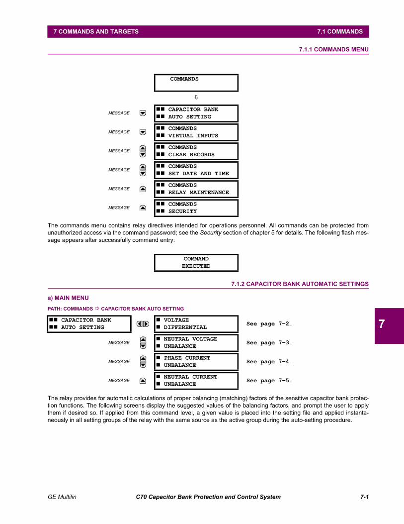
GE Multilin C70 Capacitor Bank Protection and Control System 7-1
7 COMMANDS AND TARGETS 7.1 COMMANDS
7
7 COMMANDS AND TARGETS 7.1COMMANDS 7.1.1 COMMANDS MENU
The commands menu contains relay directives intended for operations personnel. All commands can be protected fromunauthorized access via the command password; see the Security section of chapter 5 for details. The following flash mes-sage appears after successfully command entry:
7.1.2 CAPACITOR BANK AUTOMATIC SETTINGS
a) MAIN MENU
PATH: COMMANDS CAPACITOR BANK AUTO SETTING
The relay provides for automatic calculations of proper balancing (matching) factors of the sensitive capacitor bank protec-tion functions. The following screens display the suggested values of the balancing factors, and prompt the user to applythem if desired so. If applied from this command level, a given value is placed into the setting file and applied instanta-neously in all setting groups of the relay with the same source as the active group during the auto-setting procedure.
COMMANDS
MESSAGE CAPACITOR BANK AUTO SETTING
MESSAGE COMMANDS VIRTUAL INPUTS
MESSAGE COMMANDS CLEAR RECORDS
MESSAGE COMMANDS SET DATE AND TIME
MESSAGE COMMANDS RELAY MAINTENANCE
MESSAGE COMMANDS SECURITY
COMMANDEXECUTED
CAPACITOR BANK AUTO SETTING
VOLTAGE DIFFERENTIAL
See page 7–2.
MESSAGE NEUTRAL VOLTAGE UNBALANCE
See page 7–3.
MESSAGE PHASE CURRENT UNBALANCE
See page 7–4.
MESSAGE NEUTRAL CURRENT UNBALANCE
See page 7–5.
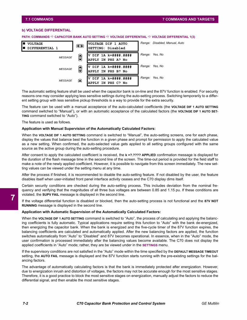
7-2 C70 Capacitor Bank Protection and Control System GE Multilin
7.1 COMMANDS 7 COMMANDS AND TARGETS
7
b) VOLTAGE DIFFERENTIAL
PATH: COMMANDS CAPACITOR BANK AUTO SETTING VOLTAGE DIFFERENTIAL VOLTAGE DIFFERENTIAL 1(3)
The automatic setting feature shall be used when the capacitor bank is on-line and the 87V function is enabled. For securityreasons one may consider applying less sensitive settings during the auto-setting process. Switching temporarily to a differ-ent setting group with less sensitive pickup thresholds is a way to provide for the extra security.
The feature can be used with a manual acceptance of the auto-calculated coefficients (the VOLTAGE DIF 1 AUTO SETTING
command switched to “Manual”), or with an automatic acceptance of the calculated factors (the VOLTAGE DIF 1 AUTO SET-
TING command switched to “Auto”).
The feature is used as follows.
Application with Manual Supervision of the Automatically Calculated Factors:
When the VOLTAGE DIF 1 AUTO SETTING command is switched to “Manual”, the auto-setting screens, one for each phase,display the values that balance best the function in a given phase and prompt for permission to apply the calculated valueas a new setting. When confirmed, the auto-selected value gets applied to all setting groups configured with the samesource as the active group during the auto-setting procedure.
After consent to apply the calculated coefficient is received, the k =?.???? APPLIED confirmation message is displayed forthe duration of the flash message time in the second line of the screen. The time-out period is provided for the field staff tomake a note of the newly applied coefficient. However, it is possible to navigate from this screen immediately. The new set-ting values can be viewed under the setting menu at any time.
After the process if finished, it is recommended to disable the auto-setting feature. If not disabled by the user, the featuredisables itself when user-initiated front panel interface activity ceases and the C70 display dims itself.
Certain security conditions are checked during the auto-setting process. This includes deviation from the nominal fre-quency and verifying that the magnitudes of all three bus voltages are between 0.85 and 1.15 pu. If these conditions areviolated. the SUPV FAIL message is displayed in the second line.
If the voltage differential function is disabled or blocked, then the auto-setting process is not functional and the 87V NOTRUNNING message is displayed in the second line.
Application with Automatic Supervision of the Automatically Calculated Factors:
When the VOLTAGE DIF 1 AUTO SETTING command is switched to “Auto”, the process of calculating and applying the balanc-ing coefficients is fully automatic. Typical applications require setting this function to “Auto” with the bank de-energized,then energizing the capacitor bank. When the bank is energized and the five-cycle timer of the 87V function expires, thebalancing coefficients are calculated and automatically applied. After the new balancing factors are applied, the functionswitches automatically from “Auto” to “Disabled” and 87V becomes operational. In essence, when in the “Auto” mode, theuser confirmation is processed immediately after the balancing values become available. The C70 does not display theapplied coefficients in “Auto” mode; rather, they are be viewed under in the SETTINGS menu.
If the supervisory conditions are not satisfied in the “Auto” mode within the time specified by the DEFAULT MESSAGE TIMEOUT
setting, the AUTO FAIL message is displayed and the 87V function starts running with the pre-existing settings for the bal-ancing factors.
The advantage of automatically calculating factors is that the bank is immediately protected after energization. However,due to energization inrush and distortion of voltages, the factors may not be accurate enough for the most sensitive stages.Therefore, it is a good practice to block the most sensitive stages on energization, manually adjust the factors to reduce thedifferential signal, and then enable the most sensitive stages.
VOLTAGE DIFFERENTIAL 1
VOLTAGE DIF 1 AUTOSETTING: Disabled
Range: Disabled, Manual, Auto
MESSAGEV DIF 1A k=####.####APPLY IN PHS A? No
Range: Yes, No
MESSAGEV DIF 1A k=####.####APPLY IN PHS B? No
Range: Yes, No
MESSAGEV DIF 1A k=####.####APPLY IN PHS C? No
Range: Yes, No

GE Multilin C70 Capacitor Bank Protection and Control System 7-3
7 COMMANDS AND TARGETS 7.1 COMMANDS
7
c) NEUTRAL VOLTAGE UNBALANCE
PATH: COMMANDS CAPACITOR BANK AUTO... NEUTRAL VOLTAGE UNBALANCE NEUTRAL VOLTAGE UNBALANCE 1(3)
The auto-setting feature shall be used when the capacitor bank is on-line and the 59NU function is enabled. For securityreasons, it may be necessary to consider applying less sensitive settings during the auto-setting process. Switching tempo-rarily to a different setting group with less sensitive pickup thresholds is a method to provide for this extra security.
This feature can be used with a manual acceptance of the auto-calculated coefficients (the NTRL VOL UNBAL 1 AUTO SET
command switched to “Manual”), or with an automatic acceptance of the calculated factors (the NTRL VOL UNBAL 1 AUTO
SET command switched to “Auto”).
The feature is used as follows.
MANUAL SUPERVISION OF AUTOMATICALLY CALCULATED FACTORS:
When the NTRL VOL UNBAL 1 AUTO SET command is switched to “Manual”, the auto-setting screens (one for each of the twofactors) display values that best balance the function and prompt for permission to apply the calculated value as a new set-ting. When confirmed, the auto-selected value is applied to all setting groups having same source as the active group dur-ing auto-setting procedure. Both ratios (XA / XB and XA / XC) must be set correctly to clear the inherent bank unbalance.After consent to apply the calculated coefficient is received via the keypad, the k =?.???? APPLIED confirmation message isdisplayed for the duration of the flash message time. The time-out period is intended for field staff to make a note of thenewly applied coefficient. However, it is possible to immediately navigate from this screen. The new setting values can beviewed in the SETTING menu at any time.
After the process if finished, it is recommended to disable the auto-setting feature. If not manually disabled, the featureautomatically disables itself when user-initiated front panel interface activity ceases and the C70 display is dimmed.
Certain security conditions are checked during the auto-setting process, such as the deviation from the nominal frequencyand the magnitude of the phase voltages within 0.85 pu and 1.15 pu. If any of these conditions are violated, the SUPV FAILmessage is displayed in the second line.
If the neutral voltage unbalance function is disabled or blocked, the auto-setting process is not functional and the 59NU NOTRUNNING message is displayed in the second line.
AUTOMATIC SUPERVISION OF AUTOMATICALLY CALCULATED FACTORS:
When the NTRL VOL UNBAL 1 AUTO SET command is switched to “Auto”, the process of calculating and applying the balanc-ing coefficients is fully automatic. Typical applications require setting this function to “Auto” with the bank de-energized,then energizing the capacitor bank. After the function is set to “Auto”, it expects to read valid input signals as a result ofbank energization within the display flash message time duration to calculate and apply factors; otherwise, the function isreturned to “Disabled”. When the bank is energized and the five-cycle timer of the 59NU function expires, the balancingcoefficients are calculated and automatically applied. When the new balancing factors are applied, the function switchesautomatically from “Auto” to “Disabled” and the 59NU function becomes operational. In essence, the when in the “Auto”mode, the confirmation command is automatically executed immediately after the balancing values are available. The C70does not display the applied coefficients in the “Auto” mode; rather, they are be viewed in the SETTINGS menu.
When the supervisory conditions are not satisfied in “Auto” mode, the AUTO FAIL message is displayed and the 59NU func-tion starts running with the pre-existing settings for the balancing factors.
NEUTRAL VOLTAGE UNBALANCE 1
NTRL VOL UNBAL 1AUTO SET: Disabled
Range: Disabled, Manual, Auto
MESSAGEXA/XB RATIO k=0.0000APPLY? No
Range: Yes, No
MESSAGEXA/XC RATIO k=0.0000APPLY? No
Range: Yes, No

7-4 C70 Capacitor Bank Protection and Control System GE Multilin
7.1 COMMANDS 7 COMMANDS AND TARGETS
7
d) PHASE CURRENT UNBALANCE
PATH: COMMANDS CAPACITOR BANK AUTO SETTINGS PHASE CURRENT UNBALANCE PHASE CURRENT UNBALANCE 1(3)
The auto-setting feature shall be used when the capacitor bank is on-line and the 60P function is enabled. For security rea-sons, it may be necessary to apply less sensitive settings during the auto-setting process. Switching temporarily to an alter-nate setting group with less sensitive pickup thresholds is a method to provide for this extra security.
The feature can be used with by manual accepting the auto-calculated coefficients (the CUR UNBALACE 1 AUTO SETTINGS
command switched to “Manual”) or by automatic acceptance of the calculated factors (the CUR UNBALACE 1 AUTO SETTINGS
command switched to “Auto”).
The feature is used as follows.
Application with Manual Supervision of the Automatically Calculated Factors:
When the CUR UNBALACE 1 AUTO SETTINGS command is switched to “Manual”, the auto-setting screens (one for eachphase) display values that best balance the function in a given phase and prompt for permission to apply the calculatedvalue as a new setting. When confirmed, the auto-selected value is applied to all setting groups having same source asactive group during the auto-setting procedure. Note that the balancing factors can be either positive or negative, depend-ing on which of the two banks has a lower impedance, and on the polarity of the differential CTs connected to the relay.
After user consent to apply the calculated coefficient is received, the k =?.???? APPLIED confirmation message is displayedfor the duration of the flash message time. The timeout period is meant for field staff to make a note of the newly appliedcoefficient. However, it is possible to immediately navigate from this screen. The new setting values can be viewed in theSETTING menu at any time.
After the process is finished, it is recommended to disable the auto-setting feature. If not disabled, the feature automaticallydisables itself when user-initiated front panel interface activity ceases and the C70 display is dimmed.
Certain security conditions are checked during the auto-setting process, such as frequency deviation from the nominal andthe magnitude of the phase currents above 0.25 pu. If any of these conditions are violated, the SUPV FAIL message is dis-played in the second line.
If the phase unbalance function is disabled or blocked, the auto-setting process is not functional and the 60P NOT RUNNINGmessage is displayed in the second line.
Application with Automatic Supervision of the Automatically Calculated Factors:
When the CUR UNBALACE 1 AUTO SETTINGS command is switched to “Manual”, the process of calculating and applying thebalancing coefficients is fully automatic. Typical applications require setting this function to “Auto” with the bank de-ener-gized, then subsequently energizing the capacitor bank. If the function is set to “Auto”, it expects to read valid input signalsas a result of bank energization within the flash message duration time to calculate and apply factors. Otherwise, the valueis switched backed to “Disabled”. When the bank is energized and the five-cycle timer of the 60P function expires, the bal-ancing coefficients are calculated and automatically applied. After the new balancing factors are applied, the auto-settingfunction switches “Auto” to “Disabled” and the 60P element becomes operational. When in the “Auto” mode, the automaticconfirmation command is executed immediately after the balancing values are available. The C70 does not display theapplied coefficients in “Auto” mode; rather, they can be viewed in the SETTINGS menu.
If the supervisory conditions are not satisfied in the “Auto” mode within time defined by the DEFAULT MESSAGE TIMEOUT set-ting, the AUTO FAIL message is displayed and the 60P function starts running with the pre-existing settings for the balanc-ing factors.
PHASE CURRENT UNBALANCE 1
CUR UNBALACE 1 AUTOSETTINGS: Disabled
Range: Disabled, Manual, Auto
MESSAGECUR UNB 1A k=0.0000APPLY IN PHS A? No
Range: Yes, No
MESSAGECUR UNB 1A k=0.0000APPLY IN PHS B? No
Range: Yes, No
MESSAGECUR UNB 1A k=0.0000APPLY IN PHS C? No
Range: Yes, No

GE Multilin C70 Capacitor Bank Protection and Control System 7-5
7 COMMANDS AND TARGETS 7.1 COMMANDS
7
e) NEUTRAL CURRENT UNBALANCE
PATH: COMMANDS CAPACITOR BANK AUTO... NEUTRAL CURRENT UNBALANCE NEUTRAL CURRENT UNBALANCE 1(3)
The auto-setting feature shall be used when the capacitor bank is online and the 60N function is enabled. For security rea-sons, it may be necessary to apply less sensitive settings during the auto-setting process. Temporarily switching to an alter-nate setting group with less sensitive pickup thresholds is a method of providing for this extra security.
The feature can be used with manual acceptance of the auto-calculated coefficients (the NTRL CUR UNBALACE 1 AUTO-SET
command switched to “Manual”), or with automatic acceptance of the calculated factors (the NTRL CUR UNBALACE 1 AUTO-
SET command switched to “Auto”).
The feature is used as follows.
Application with Manual Supervision of the Automatically Calculated Factors
When the NTRL CUR UNBALACE 1 AUTO-SET command is switched to “Manual”, the auto-setting screens (one for magnitudeand one for angle of the compensating factor) display the values that best balance the function and prompt for permissionto apply the calculated value as a new setting. When confirmed, the auto-selected value is applied to all setting groups.
After user consent to apply the calculated coefficient is received, the k =?.???? APPLIED confirmation message is displayedfor the duration of the flash message time. The timeout period is intended for field staff to make a note of the newly appliedcoefficient. However, it is possible to immediately navigate from this screen. The new setting values can be viewed in theSETTING menu at any time.
After the process if finished, it is recommended to disable the auto-setting feature. If not disabled by the user, the feature isautomatically disabled when user-initiated front panel interface activity ceases and the C70 display is dimmed.
Certain security conditions are checked during the auto-setting process. If these conditions are violated, the SUPV FAILmessage is displayed in the second line.
If the neutral voltage unbalance function is disabled or blocked, the auto-setting process is not functional and the 60N NOTRUNNING message is displayed in the second line.
Application with Automatic Supervision of the Automatically Calculated Factors
When the NTRL CUR UNBALACE 1 AUTO-SET command is switched to “Auto”, the process of calculating and applying the bal-ancing coefficients is fully automatic. Typical applications require setting this function to “Auto” with the bank de-energized,then subsequently energizing the capacitor bank. After the function is set to “Auto”, it expects to read valid input signals asa result of bank energization within the display flash message time duration to calculate and apply factors. Otherwise, thefunction is switched backed to “Disabled”. When the bank is energized and the five-cycle timer of the 60N function expires,the balancing coefficients are calculated and automatically applied. After the new balancing factors are applied, the auto-setting function switches automatically from “Auto” to “Disabled”, and the 60N element becomes operational. In essence,the when in the “Auto” mode, the confirmation command is automatically executed immediately after the balancing valuesbecome available. The C70 does not display the applied coefficients in the “Auto” mode; instead, they may be viewed in theSETTINGS menu.
If the supervisory conditions are not satisfied in the “Auto” mode within time defined by the DEFAULT MESSAGE TIMEOUT set-ting, the AUTO FAIL message is displayed and the 60N function starts running with the pre-existing settings for the balanc-ing factors.
NEUTRAL CURRENT UNBALANCE 1
NTRL CUR UNBALACE 1AUTO-SET: Disabled
Range: Disabled, Manual, Auto
MESSAGENTRL CUR 1 k=0.0000APPLY MAGNITUDE? No
Range: Yes, No
MESSAGENTRL CUR 1 k=0°APPLY ANGLE? No
Range: Yes, No

7-6 C70 Capacitor Bank Protection and Control System GE Multilin
7.1 COMMANDS 7 COMMANDS AND TARGETS
7
7.1.3 VIRTUAL INPUTS
PATH: COMMANDS VIRTUAL INPUTS
The states of up to 64 virtual inputs are changed here. The first line of the display indicates the ID of the virtual input. Thesecond line indicates the current or selected status of the virtual input. This status will be a state off (logic 0) or on (logic 1).
7.1.4 CLEAR RECORDS
PATH: COMMANDS CLEAR RECORDS
This menu contains commands for clearing historical data such as the event records. Data is cleared by changing a com-mand setting to “Yes” and pressing the ENTER key. After clearing data, the command setting automatically reverts to “No”.
7.1.5 SET DATE AND TIME
PATH: COMMANDS SET DATE AND TIME
The date and time can be entered here via the faceplate keypad, but if the relay is synchronizing to an external time sourcesuch as PTP, IRIGB or SNTP, the manually entered time will be quickly over-written. The time setting is based on the 24-hour clock. The complete date, as a minimum, must be entered to allow execution of this command. The new time (ifentered) and date will take effect at the moment the ENTER key is clicked.
The timescale of the entered time should be local time, including daylight time where and when applicable.
COMMANDS VIRTUAL INPUTS
Virt Ip 1Off
Range: Off, On
Virt Ip 2Off
Range: Off, On
MESSAGEVirt Ip 64Off
Range: Off, On
COMMANDS CLEAR RECORDS
CLEAR USER FAULTREPORTS? No
Range: No, Yes
CLEAR EVENT RECORDS?No
Range: No, Yes
CLEAR OSCILLOGRAPHY?No
Range: No, Yes
CLEAR DATA LOGGER?No
Range: No, Yes
CLEAR UNAUTHORIZEDACCESS? No
Range: No, Yes
CLEAR DIRECT I/OCOUNTERS? No
Range: No, Yes. Valid only for units with Direct Input/Output module.
CLEAR ALL RELAYRECORDS? No
Range: No, Yes
COMMANDS SET DATE AND TIME
SET DATE AND TIME:2000/01/14 13:47:03
(YYYY/MM/DD HH:MM:SS)

GE Multilin C70 Capacitor Bank Protection and Control System 7-7
7 COMMANDS AND TARGETS 7.1 COMMANDS
7
7.1.6 RELAY MAINTENANCE
PATH: COMMANDS RELAY MAINTENANCE
This menu contains commands for relay maintenance purposes. Commands for the lamp test and order code are activatedby changing a command setting to “Yes” and pressing the ENTER key. The command setting will then automatically revertto “No”. The service command is activated by entering a numerical code and pressing the ENTER key.
The PERFORM LAMPTEST command turns on all faceplate LEDs and display pixels for a short duration. The UPDATEORDER CODE command causes the relay to scan the backplane for the hardware modules and update the order code tomatch. If an update occurs, the following message is shown.
There is no impact if there have been no changes to the hardware modules. When an update does not occur, the ORDERCODE NOT UPDATED message will be shown.
The SERVICE COMMAND is used to perform specific C70 service actions. Presently, there is only one service action avail-able. Code “101” is used to clear factory diagnostic information stored in the non-volatile memory. If a code other than “101”is entered, the command will be ignored and no actions will be taken. Various self-checking diagnostics are performed inthe background while the C70 is running, and diagnostic information is stored on the non-volatile memory from time to timebased on the self-checking result. Although the diagnostic information is cleared before the C70 is shipped from the factory,the user may want to clear the diagnostic information for themselves under certain circumstances. For example, it may bedesirable to clear diagnostic information after replacement of hardware. Once the diagnostic information is cleared, all self-checking variables are reset to their initial state and diagnostics will restart from scratch.
The REBOOT RELAY COMMAND reboots the relay so that changes to configuration settings can take effect. In most cases, ifchanges are made to the configuration settings these changes do not take effect unless the relay is rebooted.
With the CyberSentry option, the Administrator or Operator role can initiate the Reboot Relay command.
7.1.7 SECURITY
iPATH: COMMANDS SECURITY
With the CyberSentry option, this setting is available to enable or disable the following commands:
• Administrator Logoff: Selecting ‘Yes’ allows the Supervisor to forcefully logoff an administrator session.
COMMANDS RELAY MAINTENANCE
PERFORM LAMPTEST?No
Range: No, Yes
UPDATE ORDER CODE?No
Range: No, Yes
REBOOT RELAY?No
Range: No, Yes
SERVICE COMMAND:0
Range: 0, 101
UPDATING...PLEASE WAIT
SECURITY
ADMINISTRATORLOGOFF: No
Range: Yes, No
Default: No
ENGINEERLOGOFF: No
Range: Yes, No
Default: No
OPERATORLOGOFF: No
Range: Yes, No
Default: No
CLEAR SECURITY DATA: Range: Yes, No
Default: No
NOTE

7-8 C70 Capacitor Bank Protection and Control System GE Multilin
7.1 COMMANDS 7 COMMANDS AND TARGETS
7
• Engineer Logoff: Selecting ‘Yes’ allows the Supervisor to forcefully logoff an engineer session.
• Operator Logoff: Selecting ‘Yes’ allows the Supervisor to forcefully logoff an operator session.
• Clear Security Data: Selecting ‘Yes’ allows the Supervisor to forcefully clear all the security logs and clears all theoperands associated with the self-tests.

GE Multilin C70 Capacitor Bank Protection and Control System 7-9
7 COMMANDS AND TARGETS 7.2 TARGETS
7
7.2TARGETS 7.2.1 TARGETS MENU
The status of any active targets will be displayed in the targets menu. If no targets are active, the display will read NOACTIVE TARGETS:
7.2.2 TARGET MESSAGES
When there are no active targets, the first target to become active will cause the display to immediately default to that mes-sage. If there are active targets and the user is navigating through other messages, and when the default message timertimes out (i.e. the keypad has not been used for a determined period of time), the display will again default back to the tar-get message.
The range of variables for the target messages is described below. Phase information will be included if applicable. If a tar-get message status changes, the status with the highest priority will be displayed.
If a self test error is detected, a message appears indicating the cause of the error. For example UNIT NOT PROGRAMMEDindicates that the minimal relay settings have not been programmed.
7.2.3 RELAY SELF-TESTS
a) DESCRIPTION
The relay performs a number of self-test diagnostic checks to ensure device integrity. The two types of self-tests (major andminor) are listed in the tables below. When either type of self-test error occurs, the Trouble LED Indicator will turn on and atarget message displayed. All errors record an event in the event recorder. Latched errors can be cleared by pressing theRESET key, providing the condition is no longer present.
Major self-test errors also result in the following:
• The critical fail relay on the power supply module is de-energized.
• All other output relays are de-energized and are prevented from further operation.
• The faceplate In Service LED indicator is turned off.
• A RELAY OUT OF SERVICE event is recorded.
TARGETS
MESSAGEDIGITAL ELEMENT 1:LATCHED
Displayed only if targets for this element are active.Example shown.
MESSAGEDIGITAL ELEMENT 48:LATCHED
Displayed only if targets for this element are active.Example shown.
MESSAGE
Table 7–1: TARGET MESSAGE PRIORITY STATUS
PRIORITY ACTIVE STATUS DESCRIPTION
1 OP element operated and still picked up
2 PKP element picked up and timed out
3 LATCHED element had operated but has dropped out

7-10 C70 Capacitor Bank Protection and Control System GE Multilin
7.2 TARGETS 7 COMMANDS AND TARGETS
7
b) MAJOR SELF-TEST ERROR MESSAGES
The major self-test errors are outlined in this section.
• Latched target message: Yes.
• Description of problem: Module hardware failure detected.
• How often the test is performed: Module dependent.
• What to do: Contact the factory and supply the failure code noted in the display. The “xxx” text identifies the failed mod-ule (for example, F8L).
• Latched target message: Yes.
• Description of problem: One or more installed hardware modules is not compatible with the C70 order code.
• How often the test is performed: Module dependent.
• What to do: Contact the factory and supply the failure code noted in the display. The “xxx” text identifies the failed mod-ule (for example, F8L).
• Latched target message: No.
• Description of problem: The configuration of modules does not match the order code stored in the C70.
• How often the test is performed: On power up. Afterwards, the backplane is checked for missing cards every five sec-onds.
• What to do: Check all modules against the order code, ensure they are inserted properly, and cycle control power. Ifthe problem persists, contact the factory.
• Latched target message: No.
• Description of problem: A FlexLogic equation is incorrect.
• How often the test is performed: The test is event driven, performed whenever FlexLogic equations are modified.
• What to do: Finish all equation editing and use self tests to debug any errors.
• Latched target message: No.
• Description of problem: The PRODUCT SETUP INSTALLATION RELAY SETTINGS setting indicates the C70 is not pro-grammed.
• How often the test is performed: On power up and whenever the PRODUCT SETUP INSTALLATION RELAY SETTINGS
setting is altered.
• What to do: Program all settings and then set PRODUCT SETUP INSTALLATION RELAY SETTINGS to “Programmed”.
MODULE FAILURE___:Contact Factory (xxx)
INCOMPATIBLE H/W:Contact Factory (xxx)
EQUIPMENT MISMATCH:with 2nd line detail
FLEXLOGIC ERROR:with 2nd line detail
UNIT NOT PROGRAMMED:Check Settings
GE Multilin C70 Capacitor Bank Protection and Control System 7-11
7 COMMANDS AND TARGETS 7.2 TARGETS
7
c) MINOR SELF-TEST ERROR MESSAGES
Most of the minor self-test errors can be disabled. Refer to the settings in the User-programmable self-tests section in theSettings chapter for additional details.
• Latched target message: No.
• Description of problem: A data item in a configurable GOOSE data set is not supported by the C70 order code.
• How often the test is performed: On power up.
• What to do: Verify that all the items in the GOOSE data set are supported by the C70. The EnerVista UR Setup soft-ware will list the valid items. An IEC61850 client will also show which nodes are available for the C70.
• Latched target message: No.
• Description of problem: A data item in a configurable report data set is not supported by the C70 order code.
• How often the test is performed: On power up.
• What to do: Verify that all the items in the configurable report data set are supported by the C70. The EnerVista URSetup software will list the valid items. An IEC61850 client will also show which nodes are available for the C70.
• Latched target message: Yes.
• Description of problem: The battery is not functioning.
• How often the test is performed: The battery is monitored every five seconds. The error message displays after 60 sec-onds if the problem persists.
• What to do: Return the power supply module to GE Digital Energy for battery replacement. To instead dispose of thebattery and power supply module, see the battery disposal information at the beginning of this manual.
• Latched target message: No.
• Description of problem: Direct input and output settings are configured for a ring, but the connection is not in a ring.
• How often the test is performed: Every second.
• What to do: Check direct input and output configuration and wiring.
• Latched target message: No.
• Description of problem: The Ethernet connection has failed for the specified port.
• How often the test is performed: Every five seconds.
• What to do: Check the Ethernet port connection on the switch.
IEC 61850 DATA SET:LLN0 GOOSE# Error
IEC 61850 DATA SET:LLN0 BR# Error
MAINTENANCE ALERT:Replace Battery
MAINTENANCE ALERT:Direct I/O Ring Break
MAINTENANCE ALERT:ENET PORT # OFFLINE
MAINTENANCE ALERT:**Bad IRIG-B Signal**

7-12 C70 Capacitor Bank Protection and Control System GE Multilin
7.2 TARGETS 7 COMMANDS AND TARGETS
7
• Latched target message: No.
• Description of problem: A bad IRIG-B input signal has been detected.
• How often the test is performed: Monitored whenever an IRIG-B signal is received.
• What to do: Ensure the following:
– The IRIG-B cable is properly connected.
– Proper cable functionality (that is, check for physical damage or perform a continuity test).
– The IRIG-B receiver is functioning.
– Check the input signal level (it may be less than specification).
If none of these apply, then contact the factory.
• Latched target message: No.
• Description of problem: No PTP enabled port has good PTP signal input.
• How often the test is performed: Activated when no acceptable signal is being received.
• What to do: Ensure the following:
– The Ethernet cable(s) are properly connected.
– At least one PTP grandmaster-capable clock is functioning.
– If strict PP is enabled, that entire network is PP compliant.
– The network is delivering PTP messages to the relay.
• Latched target message: No.
• Description of problem: An Ethernet connection has failed.
• How often the test is performed: Monitored every five seconds.
• What to do: Check Ethernet connections. Port 1 is the primary port and port 2 is the secondary port.
• Latched target message: No.
• Description of problem: The SNTP server is not responding.
• How often the test is performed: Every 10 to 60 seconds.
• What to do: Check SNTP configuration and network connections.
• Latched target message: No.
• Description of problem: A discrepancy has been detected between the actual and desired state of a latching contactoutput of an installed type “4L” module.
• How often the test is performed: Upon initiation of a contact output state change.
• What to do: Verify the state of the output contact and contact the factory if the problem persists.
MAINTENANCE ALERT:**Bad PTP Signal**
MAINTENANCE ALERT:Port ## Failure
MAINTENANCE ALERT:SNTP Failure
MAINTENANCE ALERT:4L Discrepancy

GE Multilin C70 Capacitor Bank Protection and Control System 7-13
7 COMMANDS AND TARGETS 7.2 TARGETS
7
• Latched target message: No.
• Description of problem: A data item in a configurable GOOSE data set is oscillating.
• How often the test is performed: Upon scanning of each configurable GOOSE data set.
• What to do: The “xxx” text denotes the data item that has been detected as oscillating. Evaluate all logic pertaining tothis item.
• Latched target message: No.
• Description of problem: A direct device is configured but not connected.
• How often the test is performed: Every second.
• What to do: Check direct input and output configuration and wiring.
• Latched target message: No.
• Description of problem: One or more GOOSE devices are not responding.
• How often the test is performed: Event driven. The test is performed when a device programmed to receive GOOSEmessages stops receiving. This can be from 1 to 60 seconds, depending on GOOSE packets.
• What to do: Check GOOSE setup.
• Latched target message: Yes.
• Description of problem: The ambient temperature is greater than the maximum operating temperature (+80°C).
• How often the test is performed: Every hour.
• What to do: Remove the C70 from service and install in a location that meets operating temperature standards.
• Latched target message: Yes.
• Description of problem: Abnormal restart from modules being removed or inserted while the C70 is powered-up, whenthere is an abnormal DC supply, or as a result of internal relay failure.
• How often the test is performed: Event driven.
• What to do: Contact the factory.
d) WRONG TRANSCEIVER MESSAGES
Description: The type of SFP does not match the CPU type.
T-type CPU = All ports support fiber SFPs only
Type: minor
Target: latched
MAINTENANCE ALERT:GGIO Ind xxx oscill
DIRECT I/O FAILURE:COMM Path Incomplete
REMOTE DEVICE FAIL:COMM Path Incomplete
TEMP MONITOR:OVER TEMPERATURE
UNEXPECTED RESTART:Press “RESET” key

7-14 C70 Capacitor Bank Protection and Control System GE Multilin
7.2 TARGETS 7 COMMANDS AND TARGETS
7
Message: "WRONG TRANSCEIVER"
A webpage "SFP Transceiver Information" is provided. This page displays the type of the SFP in it. This data is to be usedwith the CPU type to know the cause of the problem.
e) SFP X MODULE FAIL MESSAGES
Description: A faulty SFP or unplugging the SFP would generate this self test.
Type: minor
Target: self reset
Message: SFP MODULE x FAIL
The webpage "SFP Transceiver Information" described in the previous section applies for this self test as well. The "SFPModule Fail" has higher priority and it suppresses the "Ethernet Fail" target message. The "SFP MODULE FAIL FUNC-TION" setting enables/disables this self test. The target for this self test is priority-based, with the third one being the high-est priority. For example, if all three SFP modules fail, then the third SFP target is activated. If the third SFP module failureresolves, then the second SFP target is activated.
HardFiber Self-Test Error Messages
In addition to those provided by the standard UR-series devices, the UR devices implement HardFiber self-tests. These arelisted below. Any abnormal diagnostic condition indicated by the LEDs or the critical failure relay also results in a self-testmessage, so troubleshooting is described here. For other relays, such at the B95Plus, see that product’s instruction manual.
Equipment Mismatch Major Self-Test
Description: The number or type of installed hardware modules does not match the order code stored in the CPU. The stan-dard UR-series Equipment Mismatch self-test is extended to cover the possible presence of a Process Card.
Severity: Protection is not available and all contact outputs and shared outputs are de-asserted.
If this message appears, check all modules against the order code. Ensure they are inserted properly, and cycle the controlpower. If a module has intentionally been added or removed use the Update Order Code command to notify the relay thatthe current module configuration is correct.
Module Failure Major Self-Test
Description: UR-series device module hardware failure detected.
Severity: Protection is not available and all contact outputs and shared outputs are de-asserted.
If this message appears, contact the factory and supply the failure code noted in the display. Text in the message identifiesthe failed module (for example, H81). If operated on a Process Card failure, the Module Fail self-test seals-in (latches) tillthe UR-series device is restarted.
Process Bus Failure Major Self-test
Description: Mission critical data is not available via the process bus. An AC quantity is considered critical if both AC bankorigins and the crosschecking settings are other than none. This self-test is also initiated by an AC input discrepancy beingdetected. See the description of the crosschecking setting in this manual for further information. In addition, this self-testcan be initiated by user logic responding to loss of critical contact input/output or other data using the Process Bus FailureOperand user-programmable self-test setting. This setting is located in the Settings > Product Setup > User-Program-mable Self Test menu.
Severity: Protection is not available and all contact outputs and shared outputs are de-asserted.
If this message appears, first rectify any Process Bus Trouble and Brick Trouble self-test errors. Check the actual value ofthe operand referenced by the Process Bus Failure Operand setting, and if “On”, determine the cause and rectify.
Should the problem persist with the foregoing all clear, the cause must be an AC input discrepancy, which is typically theresult of problems in the input signals to the Bricks, or faults in the Brick input conditioning hardware. If the error wasannunciated the first time significant signal was encountered, suspect the former cause and check the copper connectionsexternal to the Brick. Where multiple UR-series devices have self-test errors, look for common causes.

GE Multilin C70 Capacitor Bank Protection and Control System 7-15
7 COMMANDS AND TARGETS 7.2 TARGETS
7
To further isolate AC input discrepancy errors, put the relay in test-isolated mode, then one by one, temporally change anAC bank crosschecking setting to none, until the Process Bus Failure clears. Once the problem AC bank has been identi-fied, the values from each of the two Bricks can be examined individually by temporarily mapping each to an AC bank witha single origin.
Process Bus Trouble Minor Self-Test
Description: Communications problems with one or more Bricks. The text of the message identifies the affected field units.This self-test is initiated by low received signal levels at either the Brick or Process Card end, and by the sustained failureto receive poll responses from the proper Brick.
Severity: This self-test error does not directly inhibit protection. However, the affected Brick inputs/outputs may not be avail-able to the UR-series device.
If this message appears, check the field unit actual values. An indication of equipment mismatch means that messages arebeing received from a Brick, but there is a discrepancy between the settings and the actual Brick serial number, order code,and/or core number. Check that the correct core on the correct Brick is patched through to the correct Process Card port,and that the field unit settings are correct. An indication of communications loss means that no messages are beingreceived. Check that the patching is correct, and that the Brick has power. If that is not the problem, use a professional opti-cal fiber connector cleaning kit to clean both sides of all optical fiber connections from the Process Card through to theaffected Brick. If the problem continues after cleaning, consult the factory.
Brick Trouble Minor Self-Test
Description: Brick internal self-testing has detected a trouble internal to the Brick.
Severity: This self-test error does not directly inhibit protection. However, some or all of the affected Brick inputs/outputsmay not be available to the UR-series device.
If this message appears, check the Brick environment for over/under temperatures and the voltage of its power source. Ifthe ambient temperature and supply voltage are within Brick specifications, consult the factory. Troubles resulting from aBrick output failing to respond to an output command can only be detected while the command is active, and so in this casethe target is latched. A latched target can be unlatched by pressing the faceplate reset key if the command has ended,however the output may still be non-functional.

7-16 C70 Capacitor Bank Protection and Control System GE Multilin
7.2 TARGETS 7 COMMANDS AND TARGETS
7

GE Multilin C70 Capacitor Bank Protection and Control System 8-1
8 SECURITY 8.1 USER ACCOUNTS
8
8 SECURITY 8.1USER ACCOUNTS 8.1.1 OVERVIEW
The EnerVista security management system is a role-based access control (RBAC) system that allows an administrator tomanage the privileges of multiple users. This allows for access control of UR devices by multiple personnel within a substa-tion and conforms to the principles of RBAC as defined in ANSI INCITS 359-2004. The EnerVista security managementsystem is disabled by default to allow the administrator direct access to the EnerVista software after installation. It is recom-mended that security be enabled before placing the device in service.
8.1.2 ENABLING THE SECURITY MANAGEMENT SYSTEM
The EnerVista security management system is disabled by default. This allows access to the device immediately afterinstallation. When security is disabled, all users are granted administrator access.
To enable the security system and require password use:
1. Select the Security > User Management menu item to open the user management window.
2. Check the Enable Security box in the lower-left corner to enable the security management system.
Security is now enabled for the EnerVista UR Setup software. Upon starting the software, users are now required to enter ausername and password.
8.1.3 ADDING A NEW USER
The following pre-requisites are required to add user accounts to the EnerVista security management system:
• The user adding the account must have administrator rights
• The EnerVista security management system must be enabled (previous section)
To add user accounts:
1. Select the Security > User Management menu item to open the user management window.
2. Enter a username in the User field. The username must be 4 to 20 characters in length.

8-2 C70 Capacitor Bank Protection and Control System GE Multilin
8.1 USER ACCOUNTS 8 SECURITY
8
3. Select the user access rights by enabling the check box of one or more of the fields.
The table outlines access rights.
4. Click OK to add the user account to the security management system.
8.1.4 MODIFYING USER PRIVILEGES
The following pre-requisites are required to modify user privileges in the EnerVista security management system:
• The user modifying the privileges must have administrator rights
• The EnerVista security management system must be enabled
To modify user privileges:
1. Select the Security > User Management menu item to open the user management window.
2. Locate the username in the User field.
Table 8–1: ACCESS RIGHTS SUMMARY
FIELD DESCRIPTION
Delete Entry Deletes the user account when exiting the user management window
Actual Values Allows the user to read actual values
Settings Allows the user to read setting values
Commands Allows the user to execute commands
Event Recorder Allows the user to use the digital fault recorder
FlexLogic Allows the user to read FlexLogic values
Update Info Allows the user to write to any function to which they have read privileges. When any of the Settings, Event Recorder, and FlexLogic check boxes are enabled by themselves, the user is granted read access. When any of them are enabled in conjunction with the Update Info box, they are granted read and write access. The user is not granted write access to functions that are not checked, even if the Update Info field is checked.
Admin The user is an EnerVista UR Setup administrator, therefore receiving all of the administrative rights. Exercise caution when granting administrator rights.
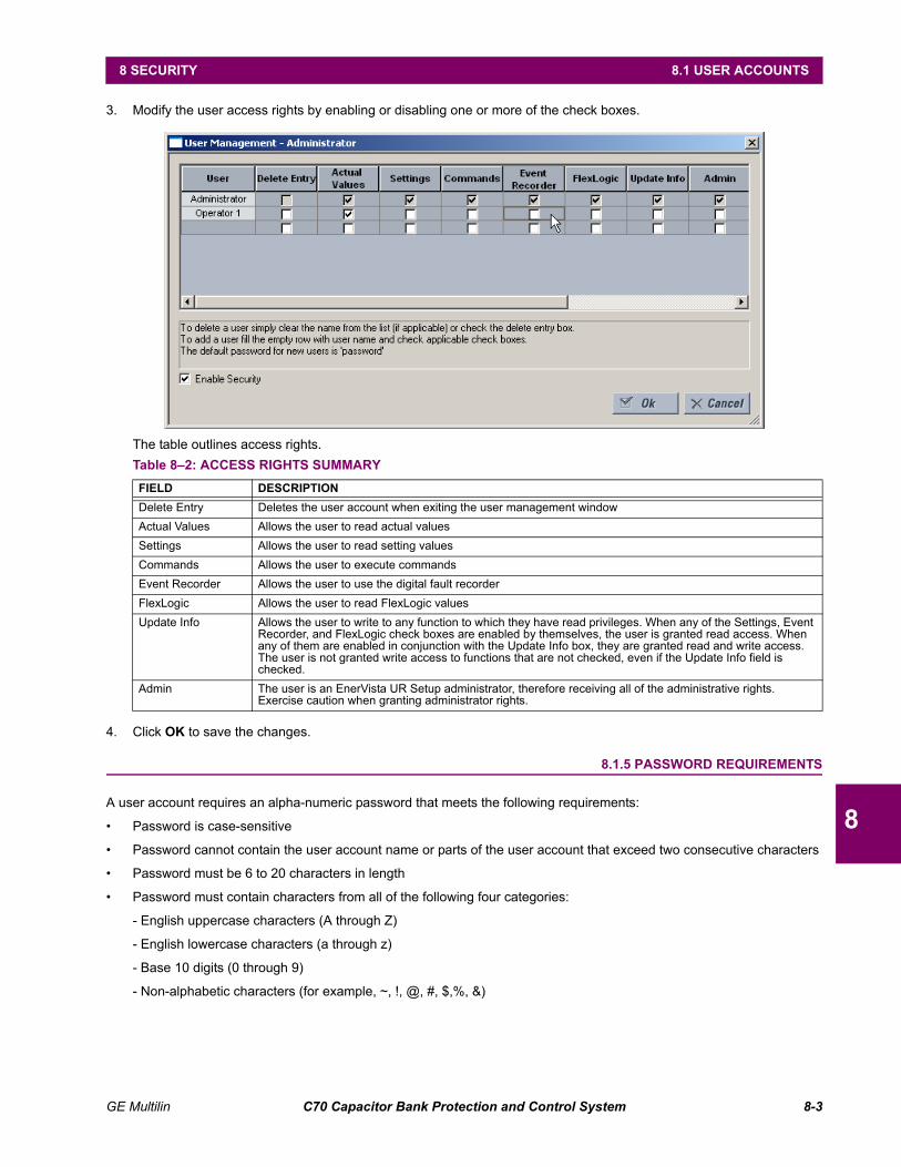
GE Multilin C70 Capacitor Bank Protection and Control System 8-3
8 SECURITY 8.1 USER ACCOUNTS
8
3. Modify the user access rights by enabling or disabling one or more of the check boxes.
The table outlines access rights.
4. Click OK to save the changes.
8.1.5 PASSWORD REQUIREMENTS
A user account requires an alpha-numeric password that meets the following requirements:
• Password is case-sensitive
• Password cannot contain the user account name or parts of the user account that exceed two consecutive characters
• Password must be 6 to 20 characters in length
• Password must contain characters from all of the following four categories:
- English uppercase characters (A through Z)
- English lowercase characters (a through z)
- Base 10 digits (0 through 9)
- Non-alphabetic characters (for example, ~, !, @, #, $,%, &)
Table 8–2: ACCESS RIGHTS SUMMARY
FIELD DESCRIPTION
Delete Entry Deletes the user account when exiting the user management window
Actual Values Allows the user to read actual values
Settings Allows the user to read setting values
Commands Allows the user to execute commands
Event Recorder Allows the user to use the digital fault recorder
FlexLogic Allows the user to read FlexLogic values
Update Info Allows the user to write to any function to which they have read privileges. When any of the Settings, Event Recorder, and FlexLogic check boxes are enabled by themselves, the user is granted read access. When any of them are enabled in conjunction with the Update Info box, they are granted read and write access. The user is not granted write access to functions that are not checked, even if the Update Info field is checked.
Admin The user is an EnerVista UR Setup administrator, therefore receiving all of the administrative rights. Exercise caution when granting administrator rights.
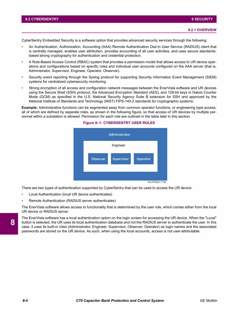
8-4 C70 Capacitor Bank Protection and Control System GE Multilin
8.2 CYBERSENTRY 8 SECURITY
8
8.2CYBERSENTRY 8.2.1 OVERVIEW
CyberSentry Embedded Security is a software option that provides advanced security services through the following:
• An Authentication, Authorization, Accounting (AAA) Remote Authentication Dial-In User Service (RADIUS) client thatis centrally managed, enables user attribution, provides accounting of all user activities, and uses secure standards-based strong cryptography for authentication and credential protection.
• A Role-Based Access Control (RBAC) system that provides a permission model that allows access to UR device oper-ations and configurations based on specific roles and individual user accounts configured on the AAA server (that is,Administrator, Supervisor, Engineer, Operator, Observer).
• Security event reporting through the Syslog protocol for supporting Security Information Event Management (SIEM)systems for centralized cybersecurity monitoring.
• Strong encryption of all access and configuration network messages between the EnerVista software and UR devicesusing the Secure Shell (SSH) protocol, the Advanced Encryption Standard (AES), and 128-bit keys in Galois CounterMode (GCM) as specified in the U.S. National Security Agency Suite B extension for SSH and approved by theNational Institute of Standards and Technology (NIST) FIPS-140-2 standards for cryptographic systems.
Example: Administrative functions can be segmented away from common operator functions, or engineering type access,all of which are defined by separate roles, as shown in the following figure, so that access of UR devices by multiple per-sonnel within a substation is allowed. Permission for each role are outlined in the table later in this section.
Figure 8–1: CYBERSENTRY USER ROLES
There are two types of authentication supported by CyberSentry that can be used to access the UR device:
• Local Authentication (local UR device authenticates)
• Remote Authentication (RADIUS server authenticates)
The EnerVista software allows access to functionality that is determined by the user role, which comes either from the localUR device or RADIUS server.
The EnerVista software has a local authentication option on the login screen for accessing the UR device. When the "Local"button is selected, the UR uses its local authentication database and not the RADIUS server to authenticate the user. In thiscase, it uses its built-in roles (Administrator, Engineer, Supervisor, Observer, Operator) as login names and the associatedpasswords are stored on the UR device. As such, when using the local accounts, access is not user-attributable.
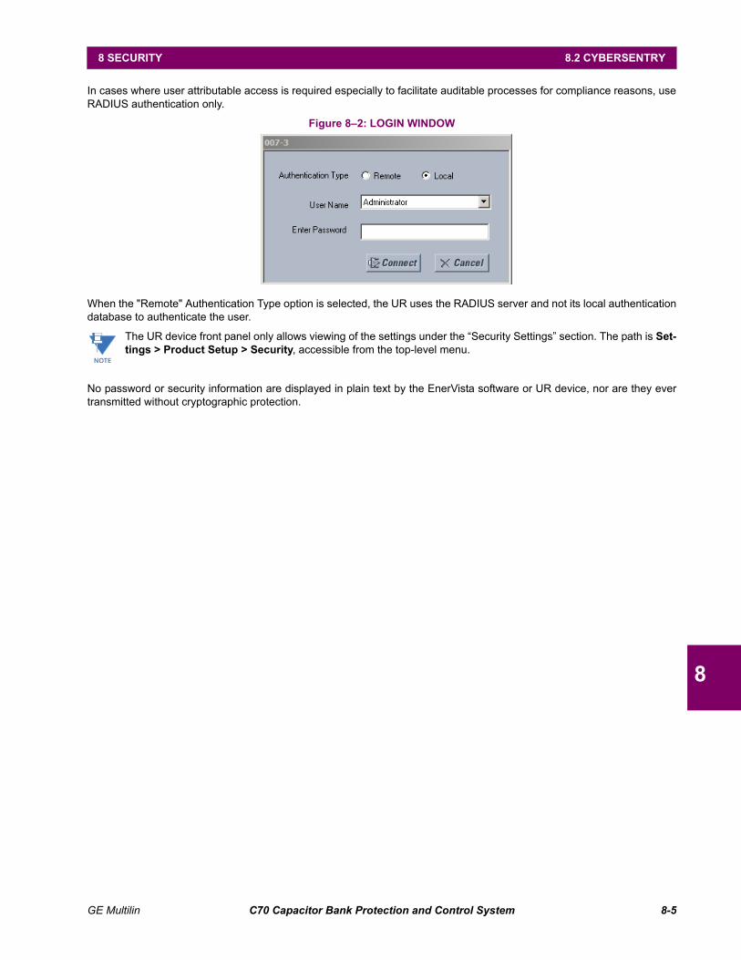
GE Multilin C70 Capacitor Bank Protection and Control System 8-5
8 SECURITY 8.2 CYBERSENTRY
8
In cases where user attributable access is required especially to facilitate auditable processes for compliance reasons, useRADIUS authentication only.
Figure 8–2: LOGIN WINDOW
When the "Remote" Authentication Type option is selected, the UR uses the RADIUS server and not its local authenticationdatabase to authenticate the user.
The UR device front panel only allows viewing of the settings under the “Security Settings” section. The path is Set-tings > Product Setup > Security, accessible from the top-level menu.
No password or security information are displayed in plain text by the EnerVista software or UR device, nor are they evertransmitted without cryptographic protection.
NOTE

8-6 C70 Capacitor Bank Protection and Control System GE Multilin
8.2 CYBERSENTRY 8 SECURITY
8
8.2.2 SECURITY MENU
a) CYBERSENTRY SECURITY SETTINGS
CyberSentry security settings are configured under Device > Settings > Product Setup > Security.
Figure 8–3: CYBERSENTRY SECURITY PANEL
The following settings are available.
RADIUS Server Settings
SETTING NAME DESCRIPTION MIN MAX DEFAULT UNITS MINIMUM PERMISSION
Primary RADIUS IP Address
IP address of the main RADIUS server. Default value indicates no Primary RADIUS server is configured, and hence RADIUS is disabled.
0.0.0.0 255.255.255.255 0.0.0.0 - Administrator
Primary Authentication Port
RADIUS authentication port 1 65535 1812 - Administrator
Primary Accounting Port
RADIUS accounting port 1 65535 1813 - Administrator
Vendor ID An identifier that specifies RADIUS vendor-specific attributes used with the protocol
Value that represents General Electric
Administrator
RADIUS Authentication (Shared) Secret
Shared secret used in authentication. It displays as asterisks. This setting must meet the CyberSentry password requirements.
See the following password section for requirements
255 characters N/A - Administrator
RADIUS Authentication Method
Authentication method used by RADIUS server. Currently fixed to EAP-TTLS.
EAP-TTLS EAP-TTLS EAP-TTLS - Administrator
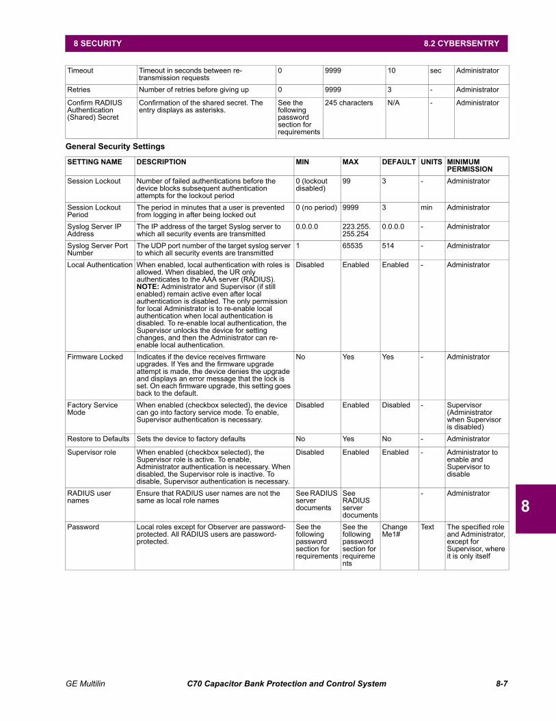
GE Multilin C70 Capacitor Bank Protection and Control System 8-7
8 SECURITY 8.2 CYBERSENTRY
8
General Security Settings
Timeout Timeout in seconds between re-transmission requests
0 9999 10 sec Administrator
Retries Number of retries before giving up 0 9999 3 - Administrator
Confirm RADIUS Authentication (Shared) Secret
Confirmation of the shared secret. The entry displays as asterisks.
See the following password section for requirements
245 characters N/A - Administrator
SETTING NAME DESCRIPTION MIN MAX DEFAULT UNITS MINIMUM PERMISSION
Session Lockout Number of failed authentications before the device blocks subsequent authentication attempts for the lockout period
0 (lockout disabled)
99 3 - Administrator
Session Lockout Period
The period in minutes that a user is prevented from logging in after being locked out
0 (no period) 9999 3 min Administrator
Syslog Server IP Address
The IP address of the target Syslog server to which all security events are transmitted
0.0.0.0 223.255.255.254
0.0.0.0 - Administrator
Syslog Server Port Number
The UDP port number of the target syslog server to which all security events are transmitted
1 65535 514 - Administrator
Local Authentication When enabled, local authentication with roles is allowed. When disabled, the UR only authenticates to the AAA server (RADIUS).NOTE: Administrator and Supervisor (if still enabled) remain active even after local authentication is disabled. The only permission for local Administrator is to re-enable local authentication when local authentication is disabled. To re-enable local authentication, the Supervisor unlocks the device for setting changes, and then the Administrator can re-enable local authentication.
Disabled Enabled Enabled - Administrator
Firmware Locked Indicates if the device receives firmware upgrades. If Yes and the firmware upgrade attempt is made, the device denies the upgrade and displays an error message that the lock is set. On each firmware upgrade, this setting goes back to the default.
No Yes Yes - Administrator
Factory Service Mode
When enabled (checkbox selected), the device can go into factory service mode. To enable, Supervisor authentication is necessary.
Disabled Enabled Disabled - Supervisor (Administrator when Supervisor is disabled)
Restore to Defaults Sets the device to factory defaults No Yes No - Administrator
Supervisor role When enabled (checkbox selected), the Supervisor role is active. To enable, Administrator authentication is necessary. When disabled, the Supervisor role is inactive. To disable, Supervisor authentication is necessary.
Disabled Enabled Enabled - Administrator to enable and Supervisor to disable
RADIUS user names
Ensure that RADIUS user names are not the same as local role names
See RADIUS server documents
See RADIUS server documents
- Administrator
Password Local roles except for Observer are password-protected. All RADIUS users are password-protected.
See the following password section for requirements
See the following password section for requirements
ChangeMe1#
Text The specified role and Administrator, except for Supervisor, where it is only itself

8-8 C70 Capacitor Bank Protection and Control System GE Multilin
8.2 CYBERSENTRY 8 SECURITY
8
Security Alarm Settings
b) PASSWORD REQUIREMENTS
See the Password Requirements section earlier.
c) USER ROLES
CyberSentry user roles (Administrator, Engineer, Operator, Supervisor, Observer) limit the levels of access to various URdevice functions. This means the EnerVista software allows for access to functionality based on the user’s logged in role.
Example: Observer cannot write any settings. The Observer role displays as "None" on the front panel.
The table lists the roles that are supported and their corresponding capabilities.
Table 8–3: PERMISSIONS BY USER ROLE FOR CYBERSENTRY
SETTING NAME DESCRIPTION / DETAILS MIN MAX DEFAULT UNITS MINIMUM PERMISSIONS
Failed Authentications
A threshold number indicating when an alarm is set off to indicate too many failed authentication attempts
0 (disabled)
99 3 - Administrator
Firmware lock A Boolean value indicating if the device can receive a firmware upgrade. If Yes and a firmware upgrade attempt is made, the device alarm activates. If No the device alarm does not activate. On each firmware upgrade this setting goes back to the default.
No Yes Yes - Administrator
Settings lock A Boolean value indicating if the device can accept any settings changes. If Yes and a settings change attempt is made, the device alarm activates. If No, the device alarm does not activate.
No Yes Yes - Supervisor (Administrator if Supervisor has been disabled)
Roles Administrator Engineer Operator Supervisor Observer
UR Setup Software Tree Menu
Complete Access Complete access except forCyberSentry Security
Command Menu
Authorizeswriting
This role is active by default
Settings
|------------ Product Setup
|--------------- Security (CyberSentry) RW R R R R
|--------------- Supervisory see table notes R R see table notes R
|--------------- Display Properties RW RW R R R
|---------------Clear relay records (settings) RW RW R R R
|--------------- Communications RW RW R R R
|--------------- Modbus user map RW RW R R R
|--------------- Real Time Clock RW RW R R R
|--------------- Oscillography RW RW R R R
|--------------- Data Logger RW RW R R R
|--------------- Demand RW RW R R R
|---------------User Programmable LEDs RW RW R R R
|---------------User Programmable self test RW RW R R R
|--------------- Control Pushbuttons RW RW R R R
|---------------User programmable Pushbuttons RW RW R R R
|--------------- Flex states RW RW R R R
|---------------User definable dis-plays RW RW R R R
|--------------- Direct I/O RW RW R R R
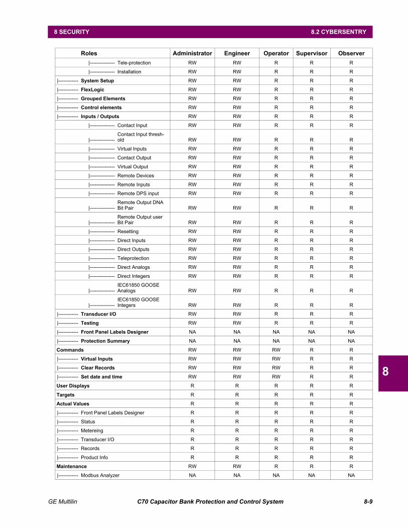
GE Multilin C70 Capacitor Bank Protection and Control System 8-9
8 SECURITY 8.2 CYBERSENTRY
8
|--------------- Tele-protection RW RW R R R
|--------------- Installation RW RW R R R
|------------ System Setup RW RW R R R
|------------ FlexLogic RW RW R R R
|------------ Grouped Elements RW RW R R R
|------------ Control elements RW RW R R R
|------------ Inputs / Outputs RW RW R R R
|--------------- Contact Input RW RW R R R
|---------------Contact Input thresh-old RW RW R R R
|--------------- Virtual Inputs RW RW R R R
|--------------- Contact Output RW RW R R R
|--------------- Virtual Output RW RW R R R
|--------------- Remote Devices RW RW R R R
|--------------- Remote Inputs RW RW R R R
|--------------- Remote DPS input RW RW R R R
|---------------Remote Output DNA Bit Pair RW RW R R R
|---------------Remote Output user Bit Pair RW RW R R R
|--------------- Resetting RW RW R R R
|--------------- Direct Inputs RW RW R R R
|--------------- Direct Outputs RW RW R R R
|--------------- Teleprotection RW RW R R R
|--------------- Direct Analogs RW RW R R R
|--------------- Direct Integers RW RW R R R
|---------------IEC61850 GOOSE Analogs RW RW R R R
|---------------IEC61850 GOOSE Integers RW RW R R R
|------------ Transducer I/O RW RW R R R
|------------ Testing RW RW R R R
|------------ Front Panel Labels Designer NA NA NA NA NA
|------------ Protection Summary NA NA NA NA NA
Commands RW RW RW R R
|------------ Virtual Inputs RW RW RW R R
|------------ Clear Records RW RW RW R R
|------------ Set date and time RW RW RW R R
User Displays R R R R R
Targets R R R R R
Actual Values R R R R R
|------------ Front Panel Labels Designer R R R R R
|------------ Status R R R R R
|------------ Metereing R R R R R
|------------ Transducer I/O R R R R R
|------------ Records R R R R R
|------------ Product Info R R R R R
Maintenance RW RW R R R
|------------ Modbus Analyzer NA NA NA NA NA
Roles Administrator Engineer Operator Supervisor Observer

8-10 C70 Capacitor Bank Protection and Control System GE Multilin
8.2 CYBERSENTRY 8 SECURITY
8
Table Notes:
1. RW = read and write access
2. R = read access
3. Supervisor = RW (default), Administrator = R (default), Administrator = RW (only if Supervisor role is disabled)
4. NA = the permission is not enforced by CyberSentry Security
d) REMOTE AUTHENTICATION
The UR has been designed to automatically direct authentication requests based on user names. In this respect, localaccount names on the UR are considered as reserved, and not provided on a RADIUS server.
The UR automatically detects whether an authentication request is to be handled remotely or locally. When an externalRADIUS server is used, the UR forwards all authentication requests for non-local user accounts to a remote RADIUSserver, and no authentication is managed at the UR itself.
As there are only five local accounts possible on the UR, if the user ID credential does not match one of the five localaccounts, the UR automatically forwards the request to a RADIUS server when one is provided.
If a RADIUS server is provided, but is unreachable over the network, remote authentication requests are denied. In this sit-uation, use local UR accounts to gain access to the UR system.
See the specific RADIUS server instructions for information on how to provide user accounts and user roles on theRADIUS server itself. User roles provided in the server must conform to those specified above.
Remote user IDs must reside on an external RADIUS server, and must be provided with the requisite user role (see the fol-lowing example). Users are specified in the RADIUS server configuration file for users. Roles are specified in the RADIUSserver dictionary.
Example:
In the file ‘users’:
exampleusername User-Password == "examplepassword"
|------------ Change Front Panel RW RW RW R R
|------------ Update Firmware Yes No No No No
|------------ Retrieve File RW R R R R
Roles Administrator Engineer Operator Supervisor Observer
NOTE
GE Multilin C70 Capacitor Bank Protection and Control System 9-1
9 THEORY OF OPERATION 9.1 OVERVIEW
9
9 THEORY OF OPERATION 9.1OVERVIEW 9.1.1 GENERAL OPERATION
Static capacitor banks are constructed with a large number of individual capacitor elements connected in a series/parallelarrangement designed to distribute the system voltage equally among the elements. Equal distribution of voltage is impor-tant as the rate of internal insulation degradation is a highly non-linear function of element voltage, with degradation accel-erating very rapidly with overvoltage greater than 10%. To obtain balanced voltages in spite of manufacturing tolerances inthe capacitance of the elements, the elements are positioned in the bank according to their actual capacitance such thatparallel groups have a uniform total capacitance, and a good voltage balance is obtained. However, once in service, individ-ual elements can fail randomly upsetting the balance, increasing the stress on other elements, and causing their early fail-ure. Early failure of an element due to unbalanced voltage predictably further unbalances the bank, leading to cascadingfailure.
The purpose of capacitor unbalance protection is to detect unbalance caused by element failures as soon as practical, andto either alarm the condition so that repair can be scheduled for a convenient time, or to automatically remove the bankfrom service to prevent deterioration in the healthy elements pending repair. A brut force method would be to directly mea-sure the voltage across each element, operating on detecting an abnormally high voltage on any element. However, thisapproach is seldom economic due to the large number of voltage transducers required. Thus, the C70 supports variousother methods, the suitability of each dependant on the capacitor bank configuration, and on the VTs and CTs available.
The challenge faced by all capacitor unbalance protections not using the brut force method is the increased sensitivityrequired due to the less than ideal number of monitoring points, and compensation for the increased effects of inherentunbalance due to manufacturing tolerance and due to system voltage unbalance.
9.1.2 BANK PHASE OVERVOLTAGE (ANSI 59B)
The capacitor unbalance protection functions discussed in the following sections are intended to detect failures in thecapacitor bank itself that can result in a few capacitor elements being overstressed. However, these unbalance protectionfunctions do not detect overstressed elements in a healthy bank that can result from external problems. Protection againstoverstressing elements from system overvoltages is instead provided by the bank phase overvoltage protection.
Ideally, a bank overvoltage protection should measure the voltage across each capacitor string, allowing an accurate infer-ence of the voltage across each element in the string, assuming that the string voltage is equally divided across the ele-ments. This is readily done in grounded wye capacitor banks by simply measuring the three system phase-to-groundvoltages. For instance assuming the bank is healthy, the elements shown in the grounded banks of the figure below willeach be stressed at one-ninth of system phase-to-ground voltage, allowing the inference that the elements are over-stressed when the system phase-to-ground voltage exceeds nine times the element safe operating voltage limit. The trueRMS value of these phase-to-ground quantities are what the bank phase overvoltage protection measures when the bussource is set for wye VTs and the bank overvoltage protection ground setpoint is set to grounded.

9-2 C70 Capacitor Bank Protection and Control System GE Multilin
9.1 OVERVIEW 9 THEORY OF OPERATION
9
Figure 9–1: BANK OVERVOLTAGE PROTECTION FOR GROUNDED AND UNGROUNDED BANKS
For a capacitor bank that is ungrounded the voltage across the string is equal to the difference between the system phase-to-ground voltage and the bank neutral voltage. For instance elements shown in the ungrounded banks in the above figurewill be overstressed when the quantities below exceed nine times the element safe operating voltage limit.
(EQ 9.1)
These quantities are what the bank phase overvoltage protection measures when the bus source is set for wye VTs, theauxiliary channel of the neutral source is set for a neutral voltage, and the bank overvoltage protection ground setpoint isset to ungrounded.
When the neutral voltage of an ungrounded wye capacitor bank is not measured or for some reason it is desired not to usethe neutral voltage measurement, the string voltage can still be determined using the assumption that the bank is balanced.For an balanced ungrounded bank the neutral voltage VX is:
(EQ 9.2)
As such, the A-string voltage is:
(EQ 9.3)
Similarly, the B-string and C-string voltages are:
(EQ 9.4)
These quantities are what the bank phase overvoltage protection measures when the bus source is set for wye VTs, andthe bank overvoltage protection ground setpoint is set to “Ungrd w/o Vn”.
In applications where the bus VTs are delta connected, the bus phase-to-ground voltages and therefore the bus zerosequence voltage are unknown. However, as shown immediately above, string voltages can be determined for anungrounded balanced bank using only phase-to-phase bus voltages. In the case of a grounded bank, we can calculate thatthe A-string voltage is:
834744A1.CDR
Grounded bank
VA
A
B
C
VB
VC
VX
VA
A
B
C
VB
VC
Ungrounded bank
VA VX– RMS, VB VX– RMS, or VC VX– RMS
VX13--- VA VB VC+ + =
VA VX– RMS VA13--- VA VB VC+ + –
RMS=
13--- 2VA VB VC–– RMS=
13--- VAB VCA– RMS=
13--- VBC VAB– RMS and
13--- VCA VBC– RMS

GE Multilin C70 Capacitor Bank Protection and Control System 9-3
9 THEORY OF OPERATION 9.1 OVERVIEW
9
(EQ 9.5)
If we make the assumption that the zero-sequence voltage is negligible, which is reasonable when the system is normal(non-faulted), then the string voltages for grounded banks are the same as for the ungrounded balanced banks:
(EQ 9.6)
These quantities are what the bank phase overvoltage protection measures whenever the bus source is set for delta VTs.
9.1.3 VOLTAGE DIFFERENTIAL (ANSI 87V)
a) OPERATING PRINCIPLE
The voltage differential function is based on a voltage divider principle - a healthy capacitor string has a constant andknown match factor between its full tap (typically the bus voltage) and an auxiliary tap used by the protection. Any singleelement failure will result in a difference between the measured factor and its value when the bank is healthy. The protec-tion can be used on both grounded and ungrounded banks. For ungrounded banks, the neutral point voltage (VX) must bemeasured by the relay, and used to derive the voltage across the string.
Figure 9–2: VOLTAGE DIFFERENTIAL APPLICATION TO GROUNDED AND UNGROUNDED BANKS
The voltage differential protection uses the following operating signal for grounded banks.
(EQ 9.7)
The voltage differential protection uses the following operating signal for ungrounded banks.
(EQ 9.8)
In the above equations, kA is a match factor setting for the A-leg of the bank. The voltages are as defined in the figureabove, and are in per-unit values on the nominal bus phase-to-ground voltage base. Equation 8.7 is implemented using pri-mary voltage magnitudes, while equation 8.8 is implemented using primary voltage phasors. The protection operates whenthe operate signal is greater than the set pickup level for the set pickup delay.
Identical relations apply to phases B and C.
VA RMS13--- 3VA VB VB– VC VC– + + RMS=
13--- VA VB– VC– VA VA VB VC+ + + + RMS=
13--- VAB VCA– 3V0+ RMS=
13--- VAB VCA– RMS,
13--- VBC VAB– RMS, or
13--- VCA VBC– RMS
834750A1.CDR
Grounded bank Ungrounded bank
V2A
V1A
A
B
C
C1A
C2A
CA
VX
V2A
V1A
A
B
C
C1A
C2A
CA
VOP A V1A kAV2A–=
VOP A V1A VX– kA V2A VX– –=

9-4 C70 Capacitor Bank Protection and Control System GE Multilin
9.1 OVERVIEW 9 THEORY OF OPERATION
9
Sensitivity is the key performance parameter. The applied comparator uses a simple integration method in addition to thestandard hysteresis approach, to deal with chattering of the operating signal at the boundary of operation.
b) BALANCED CASE
To understand how the voltage differential protection works, consider for simplicity the grounded bank operating equationbelow.
(EQ 9.9)
The ungrounded case is similar except that all voltages have VX subtracted. If the initial factory balanced A-leg string hasan initial capacitance of CA, divided into sub-strings with initial capacitances of C1A and C2A, and the bank is energized withsystem phase-to-ground voltage VSpg, then the string will form a voltage divider and the initial measured voltages are:
(EQ 9.10)
(EQ 9.11)
Substituting these results into equation 8.9, the initial operating signal is:
(EQ 9.12)
The match factor setting kA is chosen as:
(EQ 9.13)
Therefore, as can be seen from the previous two equations, the initial operating signal will be zero.
c) SENSITIVITY
Now consider the consequences of an element failure in the upper sub-string of leg A, making a small capacitance changein C1A. The effect on the operating signal can be calculated by taking the derivative of equation 8.12 with respect to CA,holding C2A constant. In the general case, the derivative of the absolute value function is messy, but in our case where theinitial value is zero, the derivative of the absolute function is simply the absolute value of the derivative of its argument. Thederivative is thus:
(EQ 9.14)
Substituting equation 8.13, we have:
(EQ 9.15)
This can be written as:
(EQ 9.16)
VOP A V1A kAV2A–=
V1A VSpg=
V2A VSpg
CA
C2A----------=
VOP A V1A kAV2A–=
VSpg kAVSpg
CA
C2A----------–=
VSpg 1 kA
CA
C2A----------–=
kAC2A
CA----------=
ddCA-----------VOP 1A VSpg
ddCA----------- 1 kA
CA
C2A----------–
=
VSpgkA
C2A----------–=
VSpg
kA
C2A----------=
ddCA-----------VOP 1A VSpg
1CA-------= or dVOP 1A VSpg
dCA
CA-----------=
VOP 1A pu VSpg pu CA pu =

GE Multilin C70 Capacitor Bank Protection and Control System 9-5
9 THEORY OF OPERATION 9.1 OVERVIEW
9
In the above equation, CA(pu) is the capacitance change as a per-unit of the leg capacitance, VSpg is the system phase-to-ground voltage, and VOP(1A)(pu) is the operating signal resulting from the failure in the upper sub-string. Both voltagesare in per-unit of nominal bus phase-to-ground voltage, so VSpg can be taken as 1 when the system is normal (not faulted).Note however that under external fault conditions sensitivity may be much different from the non-fault sensitivity.
Instead of a failure in the upper sub-string, we now suppose a failure in the lower sub-string. The same approach is used,except to make the algebra easier, the initial operating signal is converted to be in terms of C1A using:
(EQ 9.17)
In this case, we have:
(EQ 9.18)
The derivative is thus:
(EQ 9.19)
Substituting equation 8.17 into equation 8.13, we have:
(EQ 9.20)
Therefore:
(EQ 9.21)
Substituting this value into equation 8.19, we get:
(EQ 9.22)
Or alternately,
(EQ 9.23)
The value can be expressed as:
(EQ 9.24)
In the above equation, CA(pu) is the capacitance change as a per-unit of the leg capacitance, VSpg is the system phase-to-ground voltage, and VOP(2A)(pu) is the operating signal resulting from the failure in the lower sub-string. Both voltagesare in per-unit of nominal bus phase-to-ground voltage, so VSpg can be taken as 1 when the system is normal (not faulted).Note however that under external fault conditions sensitivity may be much different from the non-fault sensitivity.
CAC1AC2A
C1A C2A+---------------------------= or C2A
CAC1A
C1A CA–------------------------=
VOP A VSpg 1 kA
CA
C2A----------–=
VSpg 1 kA
C1A CA–
C1A------------------------–=
ddCA-----------VOP 2A VSpg
ddCA----------- 1 kA
C1A CA–
C1A------------------------–
=
VSpgkA
C1A----------=
VSpg
kA
C1A----------=
kAC2A
CA----------
C1A
C1A CA–------------------------= = or C1A kAC1A kACA–=
C1AkACA
kA 1–---------------=
ddCA-----------VOP 2A VSpg
kA
C1A----------=
VSpg
kA 1–
CA---------------=
dVOP 2A VSpg= kA 1– dCA
CA-----------
VOP 2A pu VSpg pu kA 1– CA pu =

9-6 C70 Capacitor Bank Protection and Control System GE Multilin
9.1 OVERVIEW 9 THEORY OF OPERATION
9
In practice, kA is no less than 2.0 as the tap is no more than half way up the phase string. Comparing equation 8.16 withequation 8.24, it can be seen that VOP(2A)(pu) VOP(1A)(pu), and thus that an element failure in the lower substring pro-duces a operating signal no smaller than the same failure in the upper sub-string. Thus VOP(1A)(pu) represents the worsecase sensitivity. A failure resulting in a 0.01 pu capacitance change in the leg capacitance results in an operating signal ofat least 0.01 pu of bus phase-to-ground voltage.
d) AUTO-SETTING
While a capacitor bank may be designed to have a tap at say the mid-point or the one-third point, manufacturing tolerancesresult in the actual tap ratio being slightly different from the design target. To prevent a spurious component in the operatingsignal, the match factor settings must correspond to the actual rather than the design tap ratio. As a convenient alternativeto manually determining the optimum match factor settings, the relay can automatically calculate these settings from itsown measurements while the capacitor is in-service, as described in the Commands chapter. The C70 sets the operate sig-nal to zero in equation 8.7 or 8.8 and solves for the match factor kA using the average of several successive voltage mea-surements. This technique has the further advantage that it to a large degree compensates for instrumentation error.However, the assumption made here is that when the auto-set command is executed, the capacitor is in an acceptably bal-anced state, wherein the operating signal ought to be zero. Following the auto-set command, the protection will be measur-ing changes from the state that existed at the time the auto-set command executed.
9.1.4 COMPENSATED BANK NEUTRAL VOLTAGE UNBALANCE (ANSI 59NU)
a) OPERATING PRINCIPLE
The neutral voltage unbalance function is applicable to ungrounded banks. Fundamentally, this function responds to anovervoltage condition of the neutral-point voltage. If the capacitor bank and the power system voltages are balanced, theneutral-point voltage is zero. Should a capacitor element in the bank fail, the bank will become unbalanced and the neutralvoltage will increase.
The operate signal for the neutral voltage unbalance protection is:
(EQ 9.25)
The restraint signal for the neutral voltage unbalance protection is:
(EQ 9.26)
In the above equations, kAB and kAC represent capacitor bank unbalance ratio settings. The voltages are as defined by thefigure below, and are expressed in per-units of the nominal value of the neutral-point VT.
These equations involve phasors, not magnitudes. That is, the vector sum of the voltages is created by the protection func-tion implementing the method.
The neutral voltage unbalance protection operates when the operate signal is greater than the set pickup level and theoperate signal is greater than the set percentage of the restraint signal, all for the set pickup delay.
Sensitivity is the key performance parameter. The applied comparator uses a simple integration method in addition to thestandard hysteresis approach to deal with chattering of the operating signal at the boundary of operation. In addition aslope characteristic is used to deal with measuring errors for the involved voltages under large system unbalances such asduring a close-in external fault.
VOP13--- VX 1 kAB kAC+ + 3V0– VB 1 kAB– VC 1 kAC– + +=
VREST VX V0+=

GE Multilin C70 Capacitor Bank Protection and Control System 9-7
9 THEORY OF OPERATION 9.1 OVERVIEW
9
Figure 9–3: COMPENSATED BANK NEUTRAL OVERVOLTAGE APPLICATION
b) BALANCED CASE
To understand neutral voltage unbalance protection, we can start with Kirchhoff's current law for the neutral node of thebank:
(EQ 9.27)
This expression can be rearranged as follows.
(EQ 9.28)
Multiplying both sides by –1 / CA and substituting the sum of the phase voltages with 3V0 yields:
(EQ 9.29)
As the left hand side of this equation is equal to zero, we can subtract it from the expression inside the absolute valuebrackets in equation 8.25 to get:
(EQ 9.30)
The unbalance ratio k-values that reflect the initial or inherent bank unbalance are chosen as:
(EQ 9.31)
Therefore, as seen from the previous two equations, the initial operating signal will be zero.
834745A1.CDR
VA
-V
X
VA
A
B
C
VX
IC
IB IA
IA
+ IB
+ IC
= 0
CC
CB
CA
IA IB IC+ + jCA VA VX– jCB VB VX– jCC VC VX– + + 0= =
VX CA CB CC+ + – VACA VBCB VCCC+ + + 0=
VX CA CB CC+ + – VACA VBCA VCCA VBCB VBCA– VCCC VCCA–+ + + + + 0=
VX CA CB CC+ + – CA VA VB VC+ + VB CB CA– VC CC CA– + + + 0=
VX 1CB CC+
CA---------------------+
3V0– VB 1CB
CA-------–
VC 1CC
CA-------–
+ + 0=
VOP13--- VX 1 kAB kAC+ + 3V0– VB 1 kAB– VC 1 kAC– V– X 1
CB CC+
CA---------------------+
3V0 VB– 1CB
CA-------–
VC– 1CC
CA-------–
++ +=
13--- VX kAB
CB
CA-------– kAC
CC
CA-------–+
VBCB
CA------- kAB– VC
CC
CA------- kAC– + +=
kAB
CB
CA-------, kAC
CC
CA-------= =

9-8 C70 Capacitor Bank Protection and Control System GE Multilin
9.1 OVERVIEW 9 THEORY OF OPERATION
9
Note that the ratios of the capacitances between phase A and the two other phases are close to unity, and therefore thecorrecting factors in equation 8.25 for the B and C-phase voltages are small numbers, while the factor for the VX voltage isclose to 3. If so, equation 8.25 takes a familiar simplified form:
(EQ 9.32)
The V0 term in the operate equation can be either the neutral component in the bus voltages (one-third of the vectorial sumof the phase voltages calculated by the relay), or directly measured neutral voltage component (open-corner-delta VT volt-age).
c) SENSITIVITY
Now consider the consequences of a capacitor element failure in one leg, most conveniently leg C, making a small capaci-tance change in leg-C capacitance. The effect on the operating signal can be calculated by taking the derivative of equation8.25 with respect to CC. In the general case, the derivative of the absolute value function is messy, but in our case wherethe initial value is zero, the derivative of the absolute function is simply the absolute value of the derivative of its argument.As such, the derivative is:
(EQ 9.33)
Recall equation 8.29.
(EQ 9.34)
Differentiating this gives:
(EQ 9.35)
Substituting for VX from equation 8.34 gives:
(EQ 9.36)
This can be substituted into equation 8.33 to obtain:
(EQ 9.37)
For our purposes, , so and . This results in:
(EQ 9.38)
VOP VX V0–=
ddCC-----------VOP
13--- d
dCC----------- VX 1 kAB kAC+ + 3V0– VB 1 kAB– VC 1 kAC– + + =
13--- 1 kAB kAC+ +
dVX
dCC-----------=
VX 1CB CC+
CA---------------------+
3V0– VB 1CB
CA-------–
VC 1CC
CA-------–
+ + 0=
dVX
dCC----------- 1
CB CC+
CA---------------------+
VX1
CA------- VC–
1CA------- + 0=
ddCC-----------VX
VX VC–
CA 1CB CC+
CA---------------------+
---------------------------------------------–=
ddCC-----------VX
VX VC–
CA 1 kAB kAC+ + ------------------------------------------------–=
ddCC-----------VX
3V0 VB 1 kAB– – VC 2 kAB+ –
CA 1 kAB kAC+ + 2-------------------------------------------------------------------------------------=
ddCC-----------VOP
13--- 1 kAB kAC+ +
dVX
dCC-----------=
13---
3V0 VB 1 kAB– – VC 2 kAB+ –
CA 1 kAB kAC+ + -------------------------------------------------------------------------------------=
CA CB CC kAB 1 kAC 1
ddCC-----------VOP
13--- VC V0–
CC--------------------
13--- 1
CC------- VC V0–=

GE Multilin C70 Capacitor Bank Protection and Control System 9-9
9 THEORY OF OPERATION 9.1 OVERVIEW
9
Under normal system conditions (non-fault), VC >> V0, and VC is the system phase-to-ground voltage. The system voltageVSpg, which by convention is on the bus voltage base, converted to the base of nominal value of the neutral-point VT usedin these equations, is:
(EQ 9.39)
This gives:
(EQ 9.40)
This can be written as:
(EQ 9.41)
In the above equations, C(pu) is the capacitance change as a per-unit of the leg capacitance, and VOP(pu) is the operatingsignal resulting from the failure in per-unit of the nominal value of the neutral-point VT. VSpg is the system phase-to-groundvoltage in per-unit of the nominal system phase-to-ground voltage, so can be taken as 1 when the system is normal (notfaulted). Note however that under external fault conditions sensitivity may be much different from the non-fault sensitivity.nbus_phs and nntrl_aux are the VT ratios of the phase VT bank of the bus source and of the auxiliary VT channel of the neutralsource, respectively.
Note that under external fault conditions sensitivity may be much different form the non-fault sensitivity. To prevent mis-operation, a restraint and/or coordinating time delay should be used.
d) RESTRAINT
Severe system voltage unbalance, such as can occur during near-by bolted ground faults, can exacerbate measurementerror in VX or V0, resulting in spurious operating signal. In addition as discussed above the sensitivity can be affected. Toprevent operation under these conditions, percent restraint supervision is provided using a restraint signal that is the mag-nitude of the vector sum of VX and V0, as defined below.
(EQ 9.42)
During external ground faults, these two voltages are approximately in phase generating a large restraining signal beingtwice the zero-sequence voltage at the bus. A slope of few percent is typically sufficient to provide good security underlarge system unbalances.
Figure 9–4: NEUTRAL OVERVOLTAGE RESTRAINT
e) AUTO-SETTING COMMAND
As a convenient alternative to manually determining the unbalance ratio settings, the relay can automatically calculatethese settings from its own measurements while the capacitor is in-service, as described in the Commands chapter. Thetechnique the relay uses is to set the operate signal variable in equation 8.25 to zero and solve for the unbalance ratio k-values using the average of several successive measurements of the voltages.
nbus_phs
nntrl_aux-------------------- VSpg
ddCC-----------VOP
13--- 1
CC-------
nbus_phs
nntrl_aux-------------------- VSpg
dVOP13---
nbus_phs
nntrl_aux-------------------- VSpg
dCC
CC-----------
VOP pu 13---
nbus_phs
nntrl_aux-------------------- VSpg C pu
VREST VX V0+=
834746A1.CDR
VREST
VOP
NTRL VOLT PKP
Slope setting
Pickup
setting
NTRL VOLT DPO

9-10 C70 Capacitor Bank Protection and Control System GE Multilin
9.1 OVERVIEW 9 THEORY OF OPERATION
9
Determination of the two k-values using only one equation is possible as the k-values are known to be real-valued, so thecomplex-valued equation above can be separated into real and imaginary parts, with the same two k-values in each. Asolution exists as long as the cross product of the B and C-phase voltages is non-zero; that is, the capacitor bank is in-ser-vice. However, the assumption made here is that when the auto-set command is executed, the capacitor is in an acceptablybalanced state, wherein the operating signal ought to be zero. Following the auto-set command, the protection will be mea-suring changes from the state that existed at the time the auto-set command executed.
9.1.5 PHASE CURRENT UNBALANCE (ANSI 60P)
a) OPERATING PRINCIPLE
The phase current unbalance function is based on the balance between interconnected and nominally identical phasestrings, and is applicable to both grounded and ungrounded installations. A window CT measuring the vectorial differencebetween the two phase currents is required for each phase as shown. While the two phase strings are actually identical, themeasured current is be zero. The failure of an element in either string results in a difference current, which is sensed by therelay. However, with the two strings slightly mismatched due to manufacturing tolerances, an inherent difference currentmay be present. Compensation for this inherent unbalance current is available to increase the sensitivity of the function.
The phase current unbalance function uses the following operate signal.
(EQ 9.43)
In this equation, kA is the capacitor bank leg-A inherent unbalance factor setting. The currents are as defined in the figurebelow, and are in per-unit on the nominal current of the differential source. This equation involve phasors, not magnitudes;that is, the vector sum of the currents is created by the protection function implementing the method.
Figure 9–5: PHASE CURRENT UNBALANCE APPLICATION
The protection operates when the operate signal is greater than the set pickup level for the set pickup delay. Identical rela-tions apply to phases B and C.
Sensitivity is the key performance parameter. The applied comparator uses a simple integration method in addition to thestandard hysteresis approach, to deal with chattering of the operating signal at the boundary of operation.
IOP A IDIF A kAIA–=
834747A1.CDR
IB1
IA
I DIF(A)
window CT
grounded or
ungrounded
CB1
IA2
CA2
IA1
CA1
IC2
CC2
IC1
CC1
IB2
CB2
IB
IC
I DIF(B)
window CT
I DIF(C)
window CT
VX
VA
GE Multilin C70 Capacitor Bank Protection and Control System 9-11
9 THEORY OF OPERATION 9.1 OVERVIEW
9
b) BALANCED CASE
To understand phase current unbalance protection, first note that the currents are driven by the individual admittances ineach string:
(EQ 9.44)
In the above equations, Ibase represents the differential CT primary current rating. This places the string currents on thesame per-unit base used by the C70. Voltages are expressed in primary volts, capacitances in Farads, and frequency inradians per second.
The differential current is the vector difference between the two currents:
(EQ 9.45)
The total phase current is the vector sum of the two currents:
(EQ 9.46)
Inserting equation 8.46 into equation 8.45, to eliminate the voltages, we get:
(EQ 9.47)
Inserting this value into equation 8.43, we have:
(EQ 9.48)
The capacitor bank leg-A inherent unbalance factor setting kA is chosen to be:
(EQ 9.49)
As can be seen from the previous two equations, the initial operating signal will be zero.
c) SENSITIVITY
Now consider the consequences of an element failure in a typical string, say string A1, making a small capacitance changein CA1 capacitance. The effect on the operating signal can be calculated by taking the derivative of equation 8.48 withrespect to CA1.
In the general case, the derivative of the absolute value function is messy, but in our case where the initial value is zero, thederivative of the absolute function is simply the absolute value of the derivative of its argument. We assume here that IA isconstant, which investigation has shown results in negligible error. The derivative is thus:
IA1
jCA1 VA VX– Ibase
------------------------------------------; IA2jCA2 VA VX–
Ibase------------------------------------------= =
IDIF A IA1 IA2–=
j VA VX– CA1 CA2– Ibase
---------------------------------------------------------------=
IA IA1 IA2+=
j VA VX– CA1 CA2+ Ibase
---------------------------------------------------------------=
IDIF A IACA1 CA2–
CA1 CA2+---------------------------=
IOP A IDIF A kAIA–=
IACA1 CA2–
CA1 CA2+--------------------------- kAIA–=
kACA1 CA2–
CA1 CA2+---------------------------=

9-12 C70 Capacitor Bank Protection and Control System GE Multilin
9.1 OVERVIEW 9 THEORY OF OPERATION
9
(EQ 9.50)
The last step assumes , and replaces the phase current vector with its magnitude. This can be written as:
(EQ 9.51)
Alternatively, we can say:
(EQ 9.52)
In the above equation, C(pu) represents the capacitance change as a per-unit of the string capacitance, and IOP(A)(pu)represents the operating signal resulting from the failure in per-unit of the nominal current of the differential source. IA isphase A terminal current on the same base. When the system is normal (no fault), IA may be taken as the capacitor bankrated primary per-phase current Irated converted to the differential source base. For example, IA = Irated / Ibase, where Ibaseis again the differential CT primary current rating, or:
(EQ 9.53)
Note that under external fault conditions, sensitivity may be much different from the non-fault sensitivity.
d) AUTO-SETTING
As a convenient alternative to manually determining inherent unbalance factor settings, the relay can automatically calcu-late these settings from its own measurements while the capacitor is in-service, as described in the Commands section ofthis manual. The technique the relay uses is to set the operate signal variable to zero in equation 8.43 and solve for theinherent unbalance factor kA using the average of several successive measurements of the currents. However, theassumption made here is that when the auto-set command is executed, the capacitor is in an acceptably balanced state,wherein the operating signal ought to be zero. Following the auto-set command, the protection will be measuring changesfrom the state that existed at the time the auto-set command executed.
9.1.6 NEUTRAL CURRENT UNBALANCE (ANSI 60N)
a) OPERATING PRINCIPLE
The neutral current unbalance function is based on the balance between interconnected neutral currents of two parallelbanks, and is applicable to both grounded and ungrounded installations. This text deals first with grounded applications,with a section at the end that discusses the differences with ungrounded applications. A window CT measuring the vectordifference between the two neutral currents is required for grounded-wye configurations.
If the two banks were identical, the inter-neutral current would be zero. The failure of an element in either bank would thenresult in inter-neutral current, which is sensed by the relay. However, with the two banks slightly mis-matched due to manu-facturing tolerances, a circulating zero-sequence current may be present. Compensation for this inherent unbalance cur-rent is available to increase the sensitivity of the function.
ddCA1--------------IOP A
ddCA1-------------- IA
CA1 CA2–
CA1 CA2+--------------------------- kAIA–
=
IACA1 CA2+ CA1 CA2– –
CA1 CA2+ 2---------------------------------------------------------------------=
IA2CA2
CA1 CA2+ 2----------------------------------=
IA2---- 1
CA1----------
CA1 CA2
dIOP A IA2----
dCA1
CA1--------------=
IOP A pu IA2---- C pu =
IOP A pu Irated
2Ibase---------------- C pu =

GE Multilin C70 Capacitor Bank Protection and Control System 9-13
9 THEORY OF OPERATION 9.1 OVERVIEW
9
Figure 9–6: NEUTRAL CURRENT UNBALANCE APPLICATION
The neutral current unbalance protection uses the following operate signal.
(EQ 9.54)
The neutral current unbalance protection uses the following restraint signal.
(EQ 9.55)
In the above equations, k1 represents the vector capacitor bank positive sequence inherent unbalance factor setting, andk1* represents the complex conjugate of k1. The currents are as defined in the figure above, and are in per-unit values ofthe nominal current of the bank source ground current channel.
These equations involve phasors, not magnitudes; that is, the vector sum of the currents is created by the protection func-tion implementing the method. The protection operates when the operate signal is greater than the set pickup level for theset pickup delay.
Sensitivity is the key performance parameter. The applied comparator uses a simple integration method in addition to thestandard hysteresis approach, to deal with chattering of the operating signal at the boundary of operation.
b) BALANCED CASE
The currents in the neutral current unbalance protection are driven by the individual admittances in each string:
834748A1.CDR
IC1
IA
IDIF
window CT
IN1
CC1
IB1
CB1
IA1
CA1
IC2
IN2
CC2
IB2
CB2
IA2
CA2
IB
IC
VC
VA
VB
grounded
configuration
IDIF
low ratio CT
IN1
IN2
VX
ungrounded
configuration
IOP IDIF k1I1 k1*I2
IREST I0

9-14 C70 Capacitor Bank Protection and Control System GE Multilin
9.1 OVERVIEW 9 THEORY OF OPERATION
9
(EQ 9.56)
In the above equations, Ibase represents the differential CT primary current rating, inserted here to put the string currents onthe same per-unit base used by the relay. Voltages are in primary volts, capacitances in Farads, and frequency in radiansper second.
The two neutral currents can be derived from the above equations:
(EQ 9.57)
The differential current is the vector difference between the two currents. By subtracting IN2 from IN1, one obtains:
(EQ 9.58)
At the same time the total currents in each phase are driven by the total admittance of the two banks in each phase:
(EQ 9.59)
Inserting the equations above into equation 8.58 so as to eliminate the voltages:
(EQ 9.60)
Label kA, kB, and kC as follows:
(EQ 9.61)
Also, convert from phase coordinates into sequence components as follows, and equation 8.60 becomes:
(EQ 9.62)
Substituting this into equation 8.54, we get:
IA1
VA jCA1Ibase
------------------------------ IA2;VA jCA2
Ibase------------------------------= =
IB1
VB jCB1Ibase
------------------------------ IB2;VB jCB2
Ibase------------------------------= =
IC1
VC jCC1Ibase
------------------------------ IC2;VC jCC2
Ibase------------------------------= =
IN1 IA1 IB1 IC1+ +jCA1VA jCB1VB jCC1VC+ +
Ibase-------------------------------------------------------------------------------------= =
IN2 IA2 IB2 IC2+ +jCA2VA jCB2VB jCC2VC+ +
Ibase-------------------------------------------------------------------------------------= =
IDIF IN1 IN2–=
j VA CA1 CA2– VB CB1 CB2– VC CC1 CC2– + + Ibase
----------------------------------------------------------------------------------------------------------------------------------------------=
IA IA1 IA2+jVA CA1 CA2+
Ibase---------------------------------------------= =
IB IB1 IB2+jVB CB1 CB2+
Ibase---------------------------------------------= =
IC IC1 IC2+jVC CC1 CC2+
Ibase----------------------------------------------= =
IDIFj VA CA1 CA2– VB CB1 CB2– VC CC1 CC2– + +
Ibase----------------------------------------------------------------------------------------------------------------------------------------------=
IACA1 CA2–
CA1 CA2+--------------------------- IB
CB1 CB2–
CB1 CB2+--------------------------- IC
CC1 CC2–
CC1 CC2+---------------------------+ +=
kA
CA1 CA2–
CA1 CA2+--------------------------- kB
CB1 CB2–
CB1 CB2+--------------------------- kC
CC1 CC2–
CC1 CC2+---------------------------= = =
IDIF kA I1 I2 I0+ + kB a2I1 aI2 I0+ + kC aI1 a
2I2 I0+ + + +=
I1 kA a2kB akC+ + I2 kA akB a
2kC+ + I0 kA kB kC+ + + +=

GE Multilin C70 Capacitor Bank Protection and Control System 9-15
9 THEORY OF OPERATION 9.1 OVERVIEW
9
(EQ 9.63)
The capacitor bank positive sequence inherent unbalance factor setting k1 is chosen to be:
(EQ 9.64)
This allows the first and second terms in the IOP equation above to vanish. The last term, being the product of two smallnumbers, virtually vanishes as well. Under normal system conditions (non-fault), the zero-sequence voltage and thus thezero-sequence current is small. The kA, kB, and kC value involve the difference between two capacitances that are factorymatched, and so are also small. In addition, it is very likely that they will be of varying signs, and thus their sum will be dou-bly small. Thus the initial operating signal under normal operating conditions is seen to be virtually zero.
c) SENSITIVITY
Now consider the consequences of an element failure in a typical string, say string A1, making a small capacitance changein the CA1 capacitance. The effect on the operating signal can be calculated by taking the derivative of equation 8.63 withrespect to CA1.
In the general case, the derivative of the absolute value function is messy, but in our case where the initial value is zero, thederivative of the absolute function is simply the absolute value of the derivative of its argument. We assume here that thecurrents remain constant, which investigation has shown results in negligible error. The derivative is thus:
(EQ 9.65)
The final step assumes , and replaces the phase current vector with its magnitude. This can be written as:
(EQ 9.66)
Alternately, we can say:
(EQ 9.67)
where C(pu) represents the capacitance change as a per-unit value of the string capacitance, and IOP(pu) represents theoperating signal resulting from the failure in per-unit of the nominal current of the differential source. IA represents thephase A terminal current on the same base. When the system is normal (no fault), IA may be taken as the capacitor bank'srated primary per-phase current Irated converted to the differential source base. For example, IA = Irated / Ibase, where Ibaseis again the differential CT primary current rating, or with system normal:
IOP IDIF k1I1 k1*I2– –=
I1 kA a2kB akC+ + I2 kA akB a
2kC+ + I0 kA kB kC+ + k1I1 k1
*I2––+ +=
I1 kA a2kB akC k1–+ + I2 kA akB a
2kC k1
*–+ + I0 kA kB kC+ + + +=
I1 kA a2kB akC k1–+ + I2 kA a
2kB akC k1–+ +
*I0 kA kB kC+ + + +=
k1 kA a2kB akC+ +=
CA1 CA2–
CA1 CA2+--------------------------- a
2CB1 CB2–
CB1 CB2+--------------------------- a
CC1 CC2–
CC1 CC2+---------------------------+ +=
ddCA1--------------IOP
ddCA1-------------- I1 kA a
2kB akC k1–+ + I2 kA a
2kB akC k1–+ +
*I0 kA kB kC+ + + + =
dkA
dCA1--------------I1
dkA
dCA1--------------I2
dkA
dCA1--------------I0+ +=
dkA
dCA1--------------IA=
CA1 CA2+ CA1 CA2– –
CA1 CA2+ 2---------------------------------------------------------------------IA=
2CA2IA
CA1 CA2+ 2----------------------------------=
IA2---- 1
CA1----------
CA1 CA2
dIOP
IA2----
dCA1
CA1--------------=
IOP pu IA2---- C pu =

9-16 C70 Capacitor Bank Protection and Control System GE Multilin
9.1 OVERVIEW 9 THEORY OF OPERATION
9
(EQ 9.68)
Note that under external fault conditions, sensitivity may be much different from the non-fault sensitivity.
d) RESTRAINT
Severe system voltage unbalance, such as can occur during near-by bolted ground faults, can exacerbate measurementerror, resulting in spurious operating signal. To prevent operation under these conditions, percent restraint supervision isapplied using a restraint signal that is the magnitude of the zero-sequence current
Typically few percent of slope is enough to ensure security of the function. The factor compensating for the inherent bankunbalance zeroes out the operating signal under relatively balanced bank currents. If the said currents contain a significantzero sequence component, the quality of compensation is lower, hence the need for the restraint, and this slope setting.
Figure 9–7: NEUTRAL CURRENT UNBALANCE RESTRAINT
e) AUTO-SETTING
As a convenient alternative to manually determining the unbalance k-factor settings, the relay can automatically calculatethese settings from its own measurements while the capacitor is in-service, as described in the Commands chapter. Thetechnique the relay uses is to set the operate signal variable to zero in equation 8.54 and solve for the unbalance factor k1using the average of several successive measurements of the currents.
However, the assumption made here is that when the auto-set command is executed, the capacitor is in an acceptably bal-anced state, wherein the operating signal ought to be zero. Following the auto-set command, the protection will be measur-ing changes from the state that existed at the time the auto-set command executed.
f) APPLICATION TO UNGROUNDED CAPACITOR BANKS
The forgoing discussion of the neutral current balance protection applied to the ground configuration. When applied toungrounded configurations, all of the above applies, with the following exceptions:
• The phase voltages in equations 8.54 through 8.59 must have the neutral voltage VX subtracted. However, as thesevoltages are eventually eliminated from the calculations, the outcome is unaffected.
• A low ratio CT can be used for ungrounded-wye configurations in place of a window type CT as there is no requirementto form the difference of the primary neutral currents.
• Whereas with the grounded configuration IDIF = IN1 – IN2, with the ungrounded configuration IDIF = IN1 = –IN2. Thisresults in the –CA2, –CB2, and –CC2 terms disappearing from equations 8.58 through 8.65. This results in the followingchanges.
Equation 8.64 becomes:
(EQ 9.69)
Equation 8.65 becomes:
IOP pu Irated
2Ibase---------------- C pu =
834749A1.CDR
I0
IOP
NTRL CUR PKP
Slope setting
Pickup
setting
NTRL CUR DPO
k1 kA a2kB akC+ +=
CA1
CA1 CA2+--------------------------- a
2 CB1
CB1 CB2+--------------------------- a
CC1
CC1 CC2+---------------------------+ +=

GE Multilin C70 Capacitor Bank Protection and Control System 9-17
9 THEORY OF OPERATION 9.1 OVERVIEW
9
(EQ 9.70)
Equation 8.67 becomes:
(EQ 9.71)
Equation 8.68 becomes:
(EQ 9.72)
Note that in the ungrounded case, the operating signal is half of that for the grounded case.
• With the grounded configuration, the two banks must be nominally identical. With the ungrounded configuration thetwo banks need not be the identical though each should be balanced. In this situation, the base for C(pu) is thecapacitance of the string which has the element failure, so the larger bank will have a lower sensitivity than the smallerbank.
ddCA1--------------IOP
CA1 CA2+ CA1–
CA1 CA2+ 2------------------------------------------------IA=
CA2IA
CA1 CA2+ 2----------------------------------=
IA4---- 1
CA1----------
IOP pu IA4---- C pu =
IOP pu Irated
4Ibase---------------- C pu =

9-18 C70 Capacitor Bank Protection and Control System GE Multilin
9.1 OVERVIEW 9 THEORY OF OPERATION
9
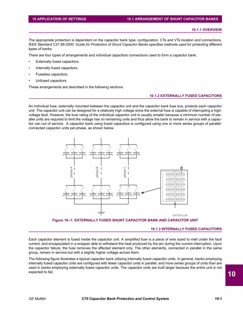
GE Multilin C70 Capacitor Bank Protection and Control System 10-1
10 APPLICATION OF SETTINGS 10.1 ARRANGEMENT OF SHUNT CAPACITOR BANKS
10
10 APPLICATION OF SETTINGS 10.1ARRANGEMENT OF SHUNT CAPACITOR BANKS 10.1.1 OVERVIEW
The appropriate protection is dependent on the capacitor bank type, configuration, CTs and VTs location and connections.IEEE Standard C37.99-2000: Guide for Protection of Shunt Capacitor Banks specifies methods used for protecting differenttypes of banks.
There are four types of arrangements and individual capacitors connections used to form a capacitor bank.
• Externally fused capacitors.
• Internally fused capacitors.
• Fuseless capacitors.
• Unfused capacitors.
These arrangements are described in the following sections.
10.1.2 EXTERNALLY FUSED CAPACITORS
An individual fuse, externally mounted between the capacitor unit and the capacitor bank fuse bus, protects each capacitorunit. The capacitor unit can be designed for a relatively high voltage since the external fuse is capable of interrupting a high-voltage fault. However, the kvar rating of the individual capacitor unit is usually smaller because a minimum number of par-allel units are required to limit the voltage rise on remaining units and thus allow the bank to remain in service with a capac-itor can out of service. A capacitor bank using fused capacitors is configured using one or more series groups of parallel-connected capacitor units per-phase, as shown below.
Figure 10–1: EXTERNALLY FUSED SHUNT CAPACITOR BANK AND CAPACITOR UNIT
10.1.3 INTERNALLY FUSED CAPACITORS
Each capacitor element is fused inside the capacitor unit. A simplified fuse is a piece of wire sized to melt under the faultcurrent, and encapsulated in a wrapper able to withstand the heat produced by the arc during the current interruption. Uponthe capacitor failure, the fuse removes the affected element only. The other elements, connected in parallel in the samegroup, remain in service but with a slightly higher voltage across them.
The following figure illustrates a typical capacitor bank utilizing internally fused capacitor units. In general, banks employinginternally fused capacitor units are configured with fewer capacitor units in parallel, and more series groups of units than areused in banks employing externally fused capacitor units. The capacitor units are built larger because the entire unit is notexpected to fail.
ph
ase
A
ph
ase
B
ph
ase
C
834753A1.CDR

10-2 C70 Capacitor Bank Protection and Control System GE Multilin
10.1 ARRANGEMENT OF SHUNT CAPACITOR BANKS 10 APPLICATION OF SETTINGS
10
Figure 10–2: INTERNALLY FUSED SHUNT CAPACITOR BANK AND CAPACITOR UNIT
10.1.4 FUSELESS CAPACITORS
Fuseless capacitor bank are typically the most prevalent designs. The capacitor units for fuseless capacitor banks are con-nected in series strings between phase and neutral. The higher the bank voltage, the more capacitor elements in series.
The expected failure of the capacitor unit element is a short circuit, where the remaining capacitor elements will absorb theadditional voltage. For example, if there are 6 capacitor units in series and each unit has 8 element groups in series there isa total of 48 element groups in the string. If one capacitor element fails, this element is shorted and the voltage across theremaining elements is 48 / 47 of the previous value, or about 2% higher. The capacitor bank remains in service; however,successive failures of elements would aggravate the problem and eventually lead to the removal of the bank.
The fuseless design is usually applied for applications at or above 34.5 kV where each string has more than ten elementsin series to ensure the remaining elements do not exceed 110% rating if an element in the string shorts.
Figure 10–3: FUSELESS SHUNT CAPACITOR BANK AND SERIES STRING
10.1.5 UNFUSED CAPACITORS
Contrary to the fuseless configuration, where the units are connected in series, the unfused shunt capacitor bank uses aseries or parallel connection of the capacitor units. The unfused approach would normally be used on banks below 34.5 kV,where series strings of capacitor units are not practical, or on higher voltage banks with modest parallel energy. This designdoes not require as many capacitor units in parallel as an externally fused bank.
ph
ase
A
ph
ase
B
ph
ase
C
834754A1.CDR
834755A1.CDR

GE Multilin C70 Capacitor Bank Protection and Control System 10-3
10 APPLICATION OF SETTINGS 10.2 CONNECTIONS OF SHUNT CAPACITOR BANKS
10
10.2CONNECTIONS OF SHUNT CAPACITOR BANKS 10.2.1 GROUNDED WYE-CONNECTED BANKS
Grounded wye capacitor banks are composed of series and parallel-connected capacitor units per-phase and provide a lowimpedance path to ground. This offers some protection from surge overvoltages and transient overcurrents.
When a capacitor bank becomes too large, making the parallel energy of a series group too high for the capacitor units orfuses (greater than 4650 kvar), the bank may be split into two wye sections. The characteristics of the grounded doublewye are similar to a grounded single wye bank. The two neutrals should be directly connected with a single path to ground.
The double-wye design facilitates better protection methods. Even with inherent unbalances the two banks will respondsimilarly to system events, and therefore, methods based on comparing one split-phase versus the other are more sensi-tive and less prone to system events (phase current balance technique, for example).
10.2.2 UNGROUNDED WYE-CONNECTED BANKS
Ungrounded wye banks do not permit zero sequence currents, third harmonic currents, or large capacitor discharge cur-rents during system ground faults (phase-to-phase faults may still occur and will result in large discharge currents). Anotheradvantage is that overvoltages appearing at the CT secondaries are not as high as in the case of grounded banks. How-ever, the neutral should be insulated for full line voltage because it is momentarily at phase potential when the bank isswitched or when one capacitor unit fails in a bank configured with a single group of units.
10.2.3 DELTA-CONNECTED BANKS
Delta-connected banks are generally used only at distribution voltages and are configured with a single series group ofcapacitors rated at line-to-line voltage. With only one series group of units, no overvoltage occurs across the remainingcapacitor units from the isolation of a faulted capacitor unit.
10.2.4 H-CONFIGURATION
Some larger banks use an H-configuration in each phase with a current transformer connected between the two legs tocompare the current down each leg. As long as all capacitors are balanced, no current will flow through the current trans-former. If a capacitor fuse operates or an element shorts, some current will flow through the current transformer. This bridgeconnection facilitates very sensitive protection. The H-arrangement is used on large banks with many capacitor units in par-allel.
10.2.5 TAPPED CONFIGURATION
Some larger banks use a tapped configuration in each phase with voltage transformers connected from the phase toground and from the tap to ground. As long as no fuses have opened and no elements have shorted, the ratio of these twovoltages will remain constant. The ratio changes with any capacitor failure in the phase, providing sensitive protection.

10-4 C70 Capacitor Bank Protection and Control System GE Multilin
10.2 CONNECTIONS OF SHUNT CAPACITOR BANKS 10 APPLICATION OF SETTINGS
10
10.2.6 SUMMARY
The following figure summarizes the grounded wye, ungrounded wye, delta, H-bridge, and tapped connection types forcapacitor banks.
Figure 10–4: CAPACITOR BANK CONNECTIONS
Grounded wye Ungrounded wye Delta
H-bridge Tapped
834756A1.CDR
GE Multilin C70 Capacitor Bank Protection and Control System 10-5
10 APPLICATION OF SETTINGS 10.3 PROTECTION METHODS FOR CAPACITOR BANKS
10
10.3PROTECTION METHODS FOR CAPACITOR BANKS 10.3.1 DESCRIPTION
The protection of shunt capacitor banks involves both bank and system protection schemes.
Bank protection schemes are provided for faults within the capacitor bank itself. Bank protection may include items such asa means to disconnect a faulted capacitor unit or capacitor elements, a means to initiate a shutdown of the bank in case offaults that may lead to a catastrophic failure, and alarms to indicate unbalance within the bank.
System protection schemes are provided to protect the capacitor bank from stresses that may be caused by the systemand to protect the substation and system from stresses that may be caused by the operation of the capacitor bank. Systemprotection may include items such as a means to limit overvoltage and excessive transient overcurrents, and to disconnectthe bank in the event of a major fault within the capacitor installation. System protection may also include alarms and meth-ods to disconnect the entire shunt capacitor bank to prevent further damage to the capacitors due to abnormal system con-ditions.
In externally fused capacitor banks, several capacitor element breakdowns may occur before the fuse removes the entireunit. The external fuse will operate when a capacitor unit becomes (essentially) short circuited, isolating the faulted unit.Unbalance protection removes the bank from service when the resulting overvoltage becomes excessive on the remaininghealthy capacitor units.
Internally fused capacitors have individual capacitor elements within a capacitor unit that are disconnected when an ele-ment breakdown occurs. The risk of successive faults is minimized because the fuse will isolate the faulty element within afew cycles. Unbalance protection removes the bank from service when the resulting unbalanced voltage becomes exces-sive on the remaining healthy capacitor elements or units.
For fuseless or unfused capacitor banks, a failed element is short-circuited by the weld that naturally occurs at the point offailure. Unbalance protection removes the bank from service when the resulting voltage becomes excessive on the remain-ing healthy capacitor elements or units.
10.3.2 CAPACITOR UNBALANCE PROTECTION
a) CONNECTIONS
Unbalance protection utilizes the unbalance that occurs in a normally balanced capacitor bank to detect an abnormality andinitiate appropriate action. The most important function is to promptly remove the bank from service for any fault that mayresult in further damage. Capacitor unbalance protection is provided in many different ways, depending on the capacitorbank arrangement.
The variety of unbalance protection schemes that may be applied with C70 for internally fused, externally fused, fuseless,or unfused shunt capacitor banks is indicated in Theory of operation chapter and is illustrated on the figures below.

10-6 C70 Capacitor Bank Protection and Control System GE Multilin
10.3 PROTECTION METHODS FOR CAPACITOR BANKS 10 APPLICATION OF SETTINGS
10
The following figure illustrates a single capacitor bank, ungrounded, with no tap available. In this case, a single CT/VT mod-ule is required.
Figure 10–5: SINGLE BANK, UNGROUNDED, NO TAP AVAILABLE
The following figure illustrates a single capacitor bank, ungrounded, with a tap. In this case, two CT/VT modules arerequired.
Figure 10–6: SINGLE BANK, UNGROUNDED, WITH A TAP
F1
-3
F5
-7
F8
50P 51P
59B 59NU
51N
C70 CAPACITOR BANK RELAY
F4
sp
are
s
834757A1.CDR
F1
-3
F5
-7
F8
50P 51P
59B 59NU
51N
C70 CAPACITOR BANK RELAY
L5
-7
87V
F4
L4
L1
-3
sp
are
s
834758A1.CDR
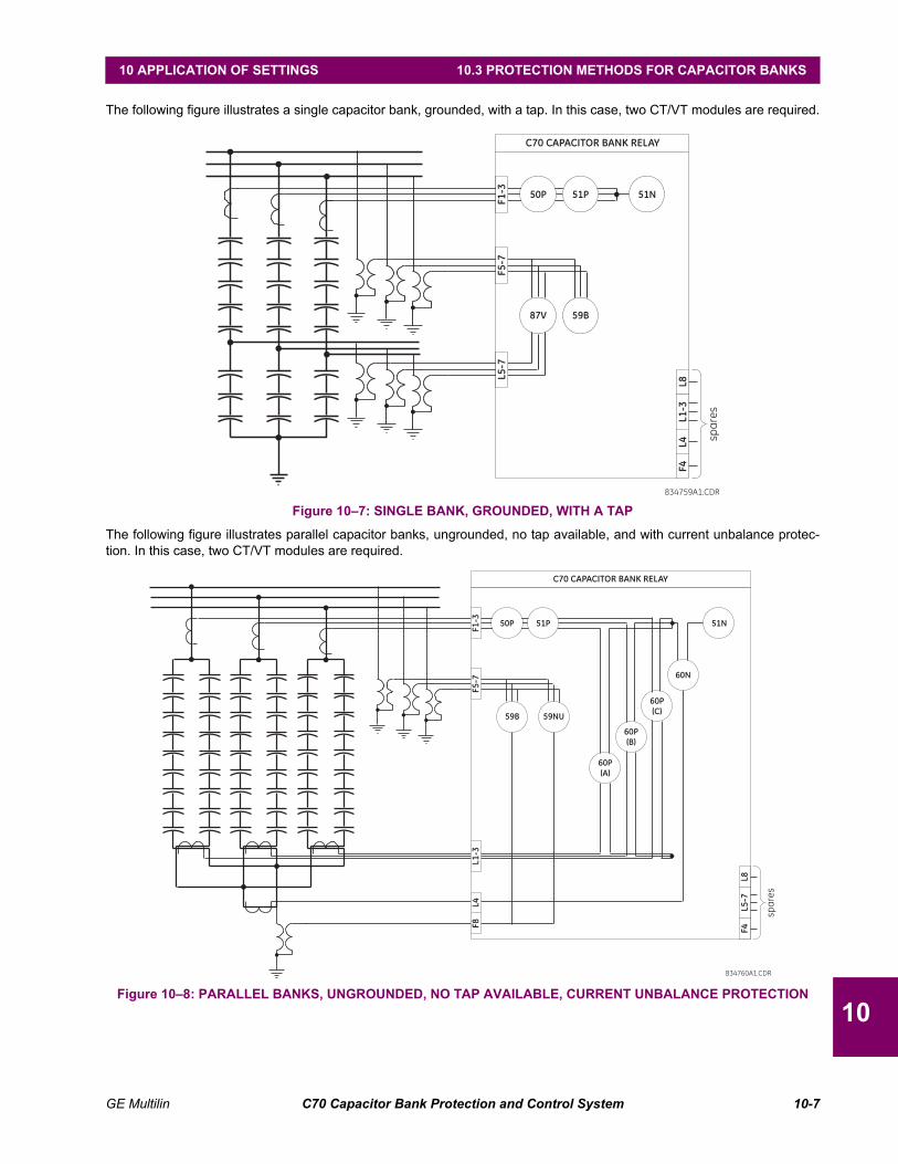
GE Multilin C70 Capacitor Bank Protection and Control System 10-7
10 APPLICATION OF SETTINGS 10.3 PROTECTION METHODS FOR CAPACITOR BANKS
10
The following figure illustrates a single capacitor bank, grounded, with a tap. In this case, two CT/VT modules are required.
Figure 10–7: SINGLE BANK, GROUNDED, WITH A TAP
The following figure illustrates parallel capacitor banks, ungrounded, no tap available, and with current unbalance protec-tion. In this case, two CT/VT modules are required.
Figure 10–8: PARALLEL BANKS, UNGROUNDED, NO TAP AVAILABLE, CURRENT UNBALANCE PROTECTION
F1
-3
F5
-7
50P 51P
59B
51N
C70 CAPACITOR BANK RELAY
L5
-7
87V
F4
L4
L1
-3
L8
sp
are
s
834759A1.CDR
F1
-3
F5
-7
F8
50P 51P
59B 59NU
51N
C70 CAPACITOR BANK RELAY
L4
L1
-3
60P
(A)
60P
(B)
60P
(C)
60N
F4
L5
-7
L8
sp
are
s
834760A1.CDR
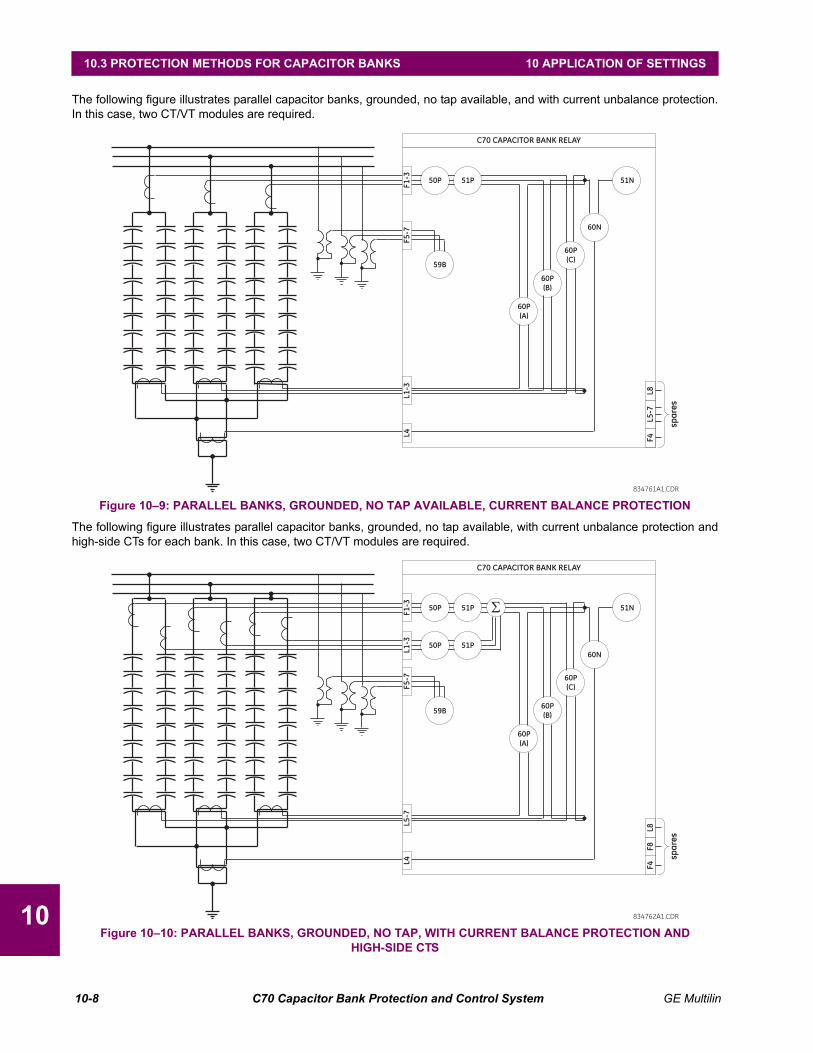
10-8 C70 Capacitor Bank Protection and Control System GE Multilin
10.3 PROTECTION METHODS FOR CAPACITOR BANKS 10 APPLICATION OF SETTINGS
10
The following figure illustrates parallel capacitor banks, grounded, no tap available, and with current unbalance protection.In this case, two CT/VT modules are required.
Figure 10–9: PARALLEL BANKS, GROUNDED, NO TAP AVAILABLE, CURRENT BALANCE PROTECTION
The following figure illustrates parallel capacitor banks, grounded, no tap available, with current unbalance protection andhigh-side CTs for each bank. In this case, two CT/VT modules are required.
Figure 10–10: PARALLEL BANKS, GROUNDED, NO TAP, WITH CURRENT BALANCE PROTECTION ANDHIGH-SIDE CTS
F1
-3
F5
-7
50P 51P
59B
51N
C70 CAPACITOR BANK RELAY
L4
L1
-3
60P
(A)
60P
(B)
60P
(C)
60N
F4
L5
-7
L8
sp
are
s
834761A1.CDR
F1
-3
F5
-7
50P 51P
59B
51N
C70 CAPACITOR BANK RELAY
L4
L5
-7
60P
(A)
60P
(B)
60P
(C)
60N
L1
-3
50P 51PF
4F
8L
8
sp
are
s
834762A1.CDR

GE Multilin C70 Capacitor Bank Protection and Control System 10-9
10 APPLICATION OF SETTINGS 10.3 PROTECTION METHODS FOR CAPACITOR BANKS
10
The following figure illustrates parallel capacitor banks, grounded, with taps and current unbalance protection. In this case,three CT/VT modules are required.
Figure 10–11: PARALLEL BANKS, GROUNDED, WITH TAPS AND CURRENT UNBALANCE PROTECTION
The normal functions of unbalance relaying are listed below.
• Trip the bank promptly if an unbalance indicates the possible presence of external arcing or a cascading fault within thecapacitor bank.
• Provide early unbalance alarm signal(s) to indicate the operation of fuses (internally or externally fused capacitors) orfailure of capacitor elements (fuseless or unfused capacitors).
• Trip the bank for unbalances that are large enough to indicate that continuing operation may result in the following.
– Damage to remaining good capacitor units or elements from overvoltage.
– Fuse malfunction.
– Inappropriate filter operation (for capacitor banks that are a part of a harmonic filter).
– Other undesirable consequences.
Note that there may be undetectable failure modes for each type of unbalance protection. These will need to be backed upby other types of protection.
b) UNBALANCE TRIP ELEMENT CONSIDERATIONS
The following points should be noted when using the unbalance trip element.
• The unbalance trip element time delay should be minimized to reduce damage from an arcing fault within the bankstructure and prevent exposure of the remaining capacitor units to overvoltage conditions beyond their permissible lim-its. For a single-phase or an open-phase condition, the time delay should also be short enough to avoid damage to thecurrent transformer or voltage transformer and to the relay system.
• The unbalance trip element should have enough time delay to avoid false operations due to inrush, system groundfaults, switching of nearby equipment, and non-simultaneous pole operation of the energizing switch. For most applica-tions, 0.1 seconds should be adequate. For unbalance relaying systems that operate on a system voltage unbalance(ground fault), a delay slightly longer than the upstream protection fault clearing time is required to avoid tripping due toa system fault. Longer delays increase the probability of catastrophic bank failure.
F1
-3
F5
-7
50P 51P
59B
51N
C70 CAPACITOR BANK RELAY
L4
L1
-3
60P
(A)
60P
(B)
60P
(C)
60N
S1
-3
,5-7
87V
87V
F4
L5
-7
L8
S4
S8
sp
are
s
834763A1.CDR

10-10 C70 Capacitor Bank Protection and Control System GE Multilin
10.3 PROTECTION METHODS FOR CAPACITOR BANKS 10 APPLICATION OF SETTINGS
10
• With grounded capacitor banks, the failure of one pole of the switching device or the single phasing from a blown bankfuse will allow zero sequence currents to flow in system ground relays. Capacitor bank relaying, including the operatingtime of the switching device, should be coordinated with the operation of the system ground relays to avoid trippingsystem load.
• The unbalance trip element may need to be delayed to account for the settling time of the protection system on initialenergization and for the transient response of certain capacitor voltage transformers, etc., which may be a part of theunbalance protection system.
• The unbalance trip scheme may include a lockout feature to prevent inadvertent closing of the capacitor bank switch-ing device if an unbalance trip has occurred.
• To allow for the effects of inherent unbalance, the unbalance element trip should be set to operate at a signal level half-way between the critical step and the next lower step. The critical step is the number of fuse operations or shorted ele-ments that will cause an overvoltage on healthy capacitor units in excess of 110% of the capacitor unit rated voltage orthe capacitor unit manufacturer's recommended maximum continuous operating voltage. In addition, for internallyfused capacitor units, the critical step may be the number of internal fuse operations at which tripping should occur asrecommended by the capacitor manufacturer.
• If switch failure or single phasing due to a blown main fuse could result in the continuous voltage exceeding the relayor VT rating, additional elements in the relay should be configured to trip the bank for this condition.
• The unbalance element detects only the unbalance in the capacitor bank and in supply voltage and will not respond tocapacitor overvoltage due to a balanced system voltage above nominal. The bank phase overvoltage should be config-ured to trip the bank for this condition.
• The maximum system operating voltage, with capacitor bank energized, should be used for setting unbalance relays.
c) UNBALANCE ALARM ELEMENT CONSIDERATIONS
To allow for the effects of inherent unbalance within the bank, the unbalance relay alarm should be set to operate at aboutone-half the level of the unbalance signal determined by the calculated alarm condition based on an idealized bank. Thealarm should have sufficient time delay to override external disturbances.
10.3.3 PROTECTION FOR RACK FAULTS (ARC-OVER WITHIN CAPACITOR BANK)
The most effective protection for an arc-over within the capacitor bank is provided by a fast unbalance element. A shorttime delay for the unbalance elements minimizes the damage caused by rack faults. Intentional delays as short as 0.05seconds have been used. This short unbalance time delay, however, should not be less than the maximum clearing time ofthe capacitor-unit or element fuse. Although the unbalance trip element is the most effective protection for arc detection ofa series section, the neutral voltage type of unbalance element should not be relied upon for rack fault protection on capac-itor banks where all three phases are not well separated.
Negative sequence elements can be used for inter-phase fault detection as they can be set to be more sensitive thanphase overcurrent relays, but tripping should be delayed to coordinate with the other relays in the system. A setting of 10%of the rated capacitor current, taking into consideration the maximum system voltage unbalance and the maximum capaci-tance variation together with a time delay setting of 15 to 25 cycles, may provide adequate coordination for faults externalto the bank. However, it may not prevent damage due to arcing faults within the bank structure.
10.3.4 OVERVOLTAGE
The capacitor bank and other equipment in the vicinity may be subjected to overvoltages resulting from abnormal systemoperating conditions. If the system voltage exceeds the capacitor or equipment capability with the capacitor bank on line,the bank should be removed with minimum time delay. Removing the capacitor bank from the system lowers the systemvoltage in the vicinity of the capacitor, reducing the overvoltage on other system elements.
Especially for very large EHV capacitor banks, it is advisable to install three-phase overvoltage protection (ANSI 59B) to tripthe bank quickly for extreme overvoltage conditions. To avoid nuisance tripping during transient overvoltage conditions, insome cases, tripping is delayed by a timer. The C70 relay provides inverse time overvoltage characteristics required todecrease tripping time for large overvoltages.
Because this tripping is not due to a fault within the capacitor bank, the capacitor bank is not locked out.

GE Multilin C70 Capacitor Bank Protection and Control System 10-11
10 APPLICATION OF SETTINGS 10.3 PROTECTION METHODS FOR CAPACITOR BANKS
10
10.3.5 OVERCURRENT
Phase and neutral time overcurrent elements can be applied with normal settings without encountering false operationsdue to inrush currents. The desirable minimum pickup is 135% of nominal phase current for grounded wye banks or 125%for ungrounded banks. Instantaneous elements (if used) should be set high to override inrush or outrush transients.
For effectively grounded systems with grounded wye capacitor banks, the high-frequency outrush current into an externalground fault will not normally operate the 51N ground element. The unbalanced capacitor bank load current caused by anexternal ground fault may be sufficient to cause the element to pick up and trip the capacitor bank if the 51N is set too low.To prevent this inadvertent tripping, the trip of the 51N element is normally set above the capacitor phase current.
10.3.6 LOSS OF BUS VOLTAGE
In some cases, it may be necessary to trip a shunt capacitor bank if the supply bus voltage is lost. Two conditions that mayneed to be considered are:
• Re-energizing a bank with a trapped charge.
• Energizing a capacitor bank without parallel load through a previously unenergized transformer.
The undervoltage element (ANSI device 27B) will detect loss of system voltage and trip the capacitor bank after a timedelay. This delay prevents tripping of the bank for system faults external to the bank. The undervoltage element should beset so the element will not operate for voltages that require the capacitor bank to remain in service. Because this tripping isalso not due to a fault within the capacitor bank (like system overvoltage tripping), the bank is not locked out.

10-12 C70 Capacitor Bank Protection and Control System GE Multilin
10.4 SETTING EXAMPLE 10 APPLICATION OF SETTINGS
10
10.4SETTING EXAMPLE 10.4.1 DESCRIPTION
Consider protection of a capacitor bank with the following characteristics:
• VLL = 138 kV fuseless.
• QB = 21 Mvar.
• Two parallel strings (S = 2) in each phase with N = 7 capacitor units rated QC = 500 kvar, VC = 11.62 kV.
• Each capacitor unit consisting of n = 6 series capacitors.
Refer to the diagram below for details. Phase capacitors are connected to ground through a neutral capacitor ratedQCN = 167 kvar, VCN = 0.825 kV.
Figure 10–12: SAMPLE CAPACITOR BANK CONFIGURATION
Based on the bank configuration, CT connections, and VTs connections, a C70 model is chosen with three CT/VT modules:two type 8L modules (in slots F and U) and one type 8V module (in slot M) to provide following protection functionality.
• Negative-sequence instantaneous overcurrent (ANSI 50_2) to provide fast backup protection against arcing withincapacitor bank.
• Phase overvoltage (ANSI 59B) to provide protection against overvoltages.
• Bank overcurrent protection, phase instantaneous overcurrent (ANSI 50P), neutral instantaneous overcurrent (ANSI50N) and phase time overcurrent (ANSI 51P) to provide protection against major faults within the capacitor bank.
• Bank undervoltage (ANSI 27P) to detect loss of bus voltage and trip the bank.
• Voltage differential (ANSI 87V) to detect failure of one or more capacitor elements in a given string. Three voltage dif-ferential elements can be set for this application: one between two tap voltages (ANSI 87V-1) and two between the busvoltage and tap voltage in both strings (ANSI 87V-2 and 87V-3).
• Phase current unbalance (ANSI 60P) to detect failure of one or more capacitor elements in a given string.
10.4.2 VT AND CT SETUP
The CT and VT connections are shown in the figure above. The CT channels are connected as follows.
• The type 8L CT/VT module F1 to F3 three-phase CT channels are connected to the bus side three-phase CTs with a120 / 5 A ratio.
F1
-3
F5
-7
59B
87V
51N
C70 CAPACITOR BANK RELAY
U1
-3
60P
(A)
60P
(B)
60P
(C)
138 kV
138 kV/
0.115 kV/
500 kvar
11620 V
120/5A
50/5A
50_250P 51P
27P
1250/250 V
167KVAR,
825V`
L4
-7
L1
-3
3
834764A1.CDR

GE Multilin C70 Capacitor Bank Protection and Control System 10-13
10 APPLICATION OF SETTINGS 10.4 SETTING EXAMPLE
10
• The type 8L CT/VT module U1 to U3 three-phase CT channels are connected to the neutral side window CTs with a50 / 5 A ratio.
The following settings are applied in the EnerVista UR Setup software.
The VT channels are connected as follows.
• The type 8L CT/VT module F5 to F7 three-phase VT channels are connected to the bus side three-phase VTs with a138 / 0.115 kV ratio.
• The type 8V CT/VT module M1 to M3 and M5 to M7 three-phase VT channels are connected to two tap VTs with a1.25 / 0.25 kV ratio. The nominal voltage is calculated below for normal bank conditions and a nominal system voltageof 138 kV (see impedance calculations the following sub-section).
The nominal bus phase VT voltage is:
(EQ 10.1)
The nominal tap VT voltage is:
(EQ 10.2)
Therefore, the tap VT secondary voltage is set as:
(EQ 10.3)
Where the VT ratio Ntap(VT) is calculated as:
(EQ 10.4)
The following settings are applied in the EnerVista UR Setup software.
10.4.3 SOURCE ASSIGNMENT
The following sources must be assigned for the protection functions indicated.
• Source 1 (bus) is assigned with CT and VT banks connected to the bus, providing a signal source for overcurrent,phase current unbalance, overvoltage, and undervoltage functions.
Vtap bus 13800
3---------------- 79674.34 V= =
Vtap nominal 138000 ZC
b
3 ZCt
--------------------------------- 13800 4.083 1894.42----------------------------------- 171.41 V= = =
Vtap secondary Vtap nominal
Ntap VT --------------------------------- 171.41 V
5------------------------ 34.28 V= = =
Ntap VT 125 kV0.25 kV-------------------- 5= =

10-14 C70 Capacitor Bank Protection and Control System GE Multilin
10.4 SETTING EXAMPLE 10 APPLICATION OF SETTINGS
10
• Source 2 (tap 1) and source 3 (tap 2) are assigned with the VT banks and split window CT bank connected to the tappoint of two strings of the bank, providing a signal source for the voltage differential and phase unbalance functions.
The CT and VT connections shown in the figure above are assigned the following values in EnerVista UR Setup.
10.4.4 BANK UNBALANCE CALCULATIONS
The following values are used in unbalance calculations.
The impedance of one capacitor can:
(EQ 10.5)
The impedance of one capacitor element, with n = 6 capacitor elements per can:
(EQ 10.6)
The impedance of the top healthy capacitor string:
(EQ 10.7)
The impedance of the bottom capacitor can:
(EQ 10.8)
The total impedance of the healthy capacitor string:
(EQ 10.9)
The maximum rated line-to-neutral system voltage:
(EQ 10.10)
The maximum rated phase current of the healthy bank:
(EQ 10.11)
The maximum rated voltage across the healthy top section:
(EQ 10.12)
The maximum rated voltage across the healthy bottom section:
ZCc VC
2
QC-------- 11.62 V 2
500 103– vars
----------------------------------------- 270.05= = =
ZCe ZC
c
n------- 270.05
6----------------------- 45.01= = =
ZCs
ZCc
N 270.05 7 1890.34= = =
ZCb VCN
2
QCN----------- 0.825 V 2
0.167 var---------------------------- 4.08 = = =
ZCt
ZCs
ZCb
+ 1890.34 4.08+ 1894.42= = =
Vmax VC NVC N
ZCs
------------------ ZCb+ 11620 V 7 11620 V 7
1890.34-------------------------------- 4.08 + 81515.37 V= = =
ImaxVmax
ZCt
2-------------- 81515.37 V
1894.92 2---------------------------------- 86.06 A= = =
VtopVmax ZC
s
ZCt
-------------------------- 81515.37 V 1890.341894.92
---------------------------------------------------------------- 81340.40 V= = =

GE Multilin C70 Capacitor Bank Protection and Control System 10-15
10 APPLICATION OF SETTINGS 10.4 SETTING EXAMPLE
10
(EQ 10.13)
The voltage distribution factor for the healthy perfectly balanced bank for the 87V-2 and 87V-3 elements:
(EQ 10.14)
The impedance of the string for the failed capacitors elements (for one failed element, nf = 1:
(EQ 10.15)
The voltage at the tap in the section with one failed capacitor element in the string:
(EQ 10.16)
The voltage of the top section with one capacitor element failed:
(EQ 10.17)
The overvoltage at the affected capacitors with one capacitor element failed:
(EQ 10.18)
The differential voltage between two taps with one failed capacitor element in the upper string, assuming K = 1 for 87V-1, inper-unit values is:
(EQ 10.19)
The differential voltage between the bus voltage and the tap with one failed capacitor element in the upper string, assumingK = 1, for 87V-3 in per-unit values is:
(EQ 10.20)
The unbalance current in the window type CT between two strings with one failed capacitor element in the upper string:
(EQ 10.21)
The following table summarizes the calculated values for the number of failed capacitors used to set the protection ele-ments.
VbottomVmax ZC
b
ZCt
-------------------------- 81515.37 V 4.08 1894.92
-------------------------------------------------------- 175.37 V= = =
KtapVtop
Vbottom------------------- 81340.40 V
175.37 V------------------------------- 463.8194= = =
ZCsf
ZCe
N n nf– ZCb
+ 45.01 7 6 1– 4.08 + 1849.41= = =
Vtap2Vmax ZC
b
ZCsf
-------------------------- 81515.37 V 4.08 1849.91
-------------------------------------------------------- 179.64 V= = =
Vtop Vmax Vtap2–=
OVVf top N n
Vtop N n nf– ----------------------------------------------- 81335.74 V 7 6
81340.40 V 7 6 1– ---------------------------------------------------------------- 1.024 pu= = =
Vdiff tap Vtap1 1 Vtap2–
VTnom tap ------------------------------------------- 175.374 V 1 179.64 V–
171.59 V------------------------------------------------------------------- 0.0249 pu= = =
Vdiff string Vf top Ktap Vtap2–
VTnom bus ----------------------------------------------------- 175.374 V 463.8194 179.64 V–
79674.34 V----------------------------------------------------------------------------------------- 0.0249 pu= = =
IunbalVmax
ZCsf
CTtap-----------------------------
Vmax
ZCs
CTtap----------------------------– 81515.37 V
1845.33 50--------------------------------------- 81515.37 V
1890.34 50---------------------------------------– 0.0209 pu= = =

10-16 C70 Capacitor Bank Protection and Control System GE Multilin
10.4 SETTING EXAMPLE 10 APPLICATION OF SETTINGS
10
To check the limits of protection sensitivity, the same calculations are repeated for the minimum system conditions, whichare considered to be 0.85 pu of nominal system voltage.
The minimum line to neutral system voltage is:
(EQ 10.22)
The following table summarizes the unbalance values during minimum system conditions.
The balance values during minimum operating conditions may be used to check sensitivity.
10.4.5 BANK VOLTAGE DIFFERENTIAL SETTINGS
The bank configuration, CT location, and VT locations allow applying three voltage differential elements:
• An 87V-1 differential element measuring the differential voltage between the two bottom taps.
• An 87V-2 differential element measuring the differential voltage between the upper capacitor string and bottom capaci-tor can for string 1.
• An 87V-3 differential element measuring the differential voltage between the upper capacitor string and bottom capaci-tor can for string 2.
Table 10–1: UNBALANCE VALUES FOR MAXIMUM SYSTEM CONDITIONS
0 1894.42 1894.42 175.37 V 175.37 V 81340.00 V 1.000 pu 0.0000 pu 0.0000 pu 0.0000 pu
1 1894.42 1849.41 175.37 V 179.64 V 81335.73 V 1.024 pu 0.0249 pu 0.0249 pu 0.0209 pu
2 1894.42 1804.40 175.37 V 184.12 V 81331.25 V 1.050 pu 0.0510 pu 0.0510 pu 0.0429 pu
3 1894.42 1759.39 175.37 V 188.83 V 81326.54 V 1.077 pu 0.0785 pu 0.0785 pu 0.0660 pu
4 1894.42 1714.38 175.37 V 193.79 V 81321.58 V 1.105 pu 0.1074 pu 0.1074 pu 0.0904 pu
5 1894.42 1669.38 175.37 V 199.01 V 81316.36 V 1.135 pu 0.1379 pu 0.1379 pu 0.1160 pu
6 1894.42 1624.37 175.37 V 204.52 V 81310.85 V 1.167 pu 0.1701 pu 0.1701 pu 0.1431 pu
7 1894.42 1579.36 175.37 V 210.35 V 81305.02 V 1.200 pu 0.2041 pu 0.2041 pu 0.1717 pu
8 1894.42 1534.35 175.37 V 216.52 V 81298.85 V 1.235 pu 0.2401 pu 0.2401 pu 0.2020 pu
9 1894.42 1489.34 175.37 V 223.07 V 81292.30 V 1.273 pu 0.2783 pu 0.2783 pu 0.2341 pu
10 1894.42 1444.34 175.37 V 230.02 V 81285.35 V 1.313 pu 0.3188 pu 0.3188 pu 0.2682 pu
Table 10–2: UNBALANCE VALUES FOR MINIMUM SYSTEM CONDITIONS
0 1894.42 1894.42 145.70 V 145.70 V 67577.30 V 1.000 pu 0.0000 pu 0.0000 pu 0.0000 pu
1 1894.42 1849.41 145.70 V 149.24 V 67573.76 V 1.024 pu 0.0207 pu 0.0207 pu 0.0174 pu
2 1894.42 1804.40 145.70 V 152.97 V 67570.03 V 1.050 pu 0.0424 pu 0.0424 pu 0.0357 pu
3 1894.42 1759.39 145.70 V 156.88 V 67566.12 V 1.077 pu 0.0652 pu 0.0652 pu 0.0549 pu
4 1894.42 1714.38 145.70 V 161.00 V 67562.00 V 1.105 pu 0.0893 pu 0.0893 pu 0.0751 pu
5 1894.42 1669.38 145.70 V 165.34 V 67557.66 V 1.135 pu 0.1146 pu 0.1146 pu 0.0964 pu
6 1894.42 1624.37 145.70 V 169.92 V 67553.08 V 1.167 pu 0.1413 pu 0.1413 pu 0.1189 pu
7 1894.42 1579.36 145.70 V 174.76 V 67548.24 V 1.200 pu 0.1696 pu 0.1696 pu 0.1426 pu
8 1894.42 1534.35 145.70 V 179.89 V 67543.11 V 1.235 pu 0.1995 pu 0.1995 pu 0.1678 pu
9 1894.42 1489.34 145.70 V 185.32 V 67537.68 V 1.273 pu 0.2312 pu 0.2312 pu 0.1945 pu
10 1894.42 1444.34 145.70 V 191.10 V 67531.90 V 1.313 pu 0.2649 pu 0.2649 pu 0.2228 pu
nf ZCs
ZCsf Vtap1 Vtap2 Vtop OV Vdiff tap Vdiff string Iunbal
Vmin0.85 Vnom
3------------------------------- 0.85 138000 V
3-------------------------------------------- 67723 V= = =
nf ZCs
ZCsf Vtap1 Vtap2 Vtop OV Vdiff tap Vdiff string Iunbal

GE Multilin C70 Capacitor Bank Protection and Control System 10-17
10 APPLICATION OF SETTINGS 10.4 SETTING EXAMPLE
10
Two voltage differential (87V) stages provide trip and alarm levels during capacitor unit failures in each differential element.The capacitor units are subject to overvoltage if one or more capacitors units are shorted out. The voltage differential trippickup setting is programmed for value of 110% of capacitor rated voltage. As seen from the Unbalance values for maxi-mum system conditions table above, a failure of four capacitor elements causes a 10.5% overvoltage.
The pickup setting for the stage 1 differential alarm element is chosen for one element failure.
(EQ 10.23)
The alarm delay is set to 10 seconds to avoid alarming during transient conditions.
The pickup setting for the stage 2 differential trip element is programmed as the differential voltage during maximum systemconditions midway between the third and fourth capacitor element failure differential voltages.
(EQ 10.24)
Therefore, the trip delay is set to 50 ms.
The following setting values for the voltage differential 1 element between two tap voltages are programmed in the EnerV-ista UR Setup software.
Note that match factor shown above assumes perfect bank balance. This must be adjusted when the bank is energizedduring the differential function auto-setting procedure tune up.
The voltage differential element must be blocked during a VT fuse failure at any tap. The voltage differential element isdependent on both source VTs. These VTs must be blocked if one or both of them has a VT fuse failure condition. There-fore, as shown in the following figure, a blocking input for each element is created with FlexLogic.
87V alarm 0.9Vdiff f1_max 0.9 0.0249 pu 0.0224 pu= = =
87V tripVdiff f4_max Vdiff f3_max +
2------------------------------------------------------------------ 0.1074 pu 0.0785 pu+
2------------------------------------------------------------ 0.093 pu= = =
10-18 C70 Capacitor Bank Protection and Control System GE Multilin
10.4 SETTING EXAMPLE 10 APPLICATION OF SETTINGS
10
Figure 10–13: VOLTAGE DIFFERENTIAL BLOCKING DURING VT FUSE FAILURE
The 87V-2 and 87V-3 differential elements for the strings against tap voltage are created in a similar manner. In thesecases, the K factor will be different, reflecting the voltage division of K = 463.8194 between the string and tap capacitor volt-ages.
10.4.6 BANK PHASE CURRENT UNBALANCE SETTINGS
Two phase current unbalance (ANSI 60P) stages are used to provide trip and alarm levels during capacitor unit failures ineach differential element.
The pickup setting for the stage 1 phase current unbalance alarm element is programmed for one element failure.
(EQ 10.25)
SRC2 VT FUSE FAIL OP
SRC3 VT FUSE FAIL OP
OR(2)
= VTFF 87V-1 (VO1)
SRC1 VT FUSE FAIL OP
SRC2 VT FUSE FAIL OP
OR(2)
= VTFF 87V-2 (VO2)
SRC1 VT FUSE FAIL OP
SRC3 VT FUSE FAIL OP
OR(2)
= VTFF 87-3 (VO3)
OR(2)
OR(2)
OR(2)
= VTFF 87V-1 (VO1)
= VTFF 87V-2 (VO2)
= VTFF 87V-3 (VO3)
843765A1.CDR
60P alarm 0.9Iunbal f1_max 0.9 0.0209 pu 0.019 pu= = =

GE Multilin C70 Capacitor Bank Protection and Control System 10-19
10 APPLICATION OF SETTINGS 10.4 SETTING EXAMPLE
10
Therefore, the alarm delay is specified as 10 seconds. The following setting values are programmed in the EnerVista URSetup software.
The pickup setting for the stage 2 current unbalance trip element is specified as the unbalance current during maximumsystem conditions midway between the third and fourth capacitor element failure unbalance currents.
(EQ 10.26)
Therefore, the trip delay is chosen 50 ms.
10.4.7 BANK PHASE OVERVOLTAGE SETTINGS
To protect the capacitor bank from overvoltage resulting from abnormal system conditions, the capability of the bank towithstand transient overvoltages must be evaluated according to the IEEE 1036-1992 standard or to manufacturer specifi-cations. For example, consider the following manufacturer overvoltage data:
• 2 pu overvoltage toleration for 0.25 second.
• 1.5 pu overvoltage toleration for 15 seconds.
• 1.25 pu overvoltage toleration for 5 minutes.
When the relay settings are calculated, the number of prospective overvoltage transients stressing the capacitor insulationduring the bank lifetime must be taken into account. As such, it is preferable to set the relay conservatively.
Based on the manufacturer overvoltage data above, three overvoltage trip stages are applied using a factor of 0.9 for thestage pickup overvoltage levels and half of the allowable time indicated above.
(EQ 10.27)
60P tripIunbal f4_max Iunbal f3_max +
2------------------------------------------------------------------------ 0.0904 pu 0.0660 pu+
2------------------------------------------------------------ 0.078 pu= = =
59B pickup (stage 1) 0.9 1.25 1.125 pu= =
59B pickup (stage 2) 0.9 1.5 1.35 pu= =
59B pickup (stage 3) 0.9 2 1.80 pu= =

10-20 C70 Capacitor Bank Protection and Control System GE Multilin
10.4 SETTING EXAMPLE 10 APPLICATION OF SETTINGS
10
(EQ 10.28)
The following setting values are programmed in the EnerVista UR Setup software.
10.4.8 BANK PHASE UNDERVOLTAGE SETTINGS
Bank undervoltage protection is required to take bank out-of-service when the supply bus voltage is lost. The pickup settingis specified as 0.7 pu with a time delay of 1 second, based on maximum fault clearing time. The bank undervoltage elementis blocked during VT fuse fail conditions.
The following setting values are programmed in the EnerVista UR Setup software.
59B delay (stage 1) 0.5 5 60 150 seconds= =
59B delay (stage 2) 0.5 15 7.5 seconds= =
59B delay (stage 3) 0.5 0.25 0.125 seconds= =

GE Multilin C70 Capacitor Bank Protection and Control System 10-21
10 APPLICATION OF SETTINGS 10.4 SETTING EXAMPLE
10
10.4.9 BANK OVERCURRENT PROTECTION
Bank overcurrent protection is required to protect capacitor banks against major faults, such as line-to-line or line-to-groundfaults. It is desirable to set overcurrent protection to be as low and as fast as possible, with only enough delay to avoid trip-ping on external system disturbances.
During bank energization, the capacitor charge current inrush may cause significant neutral currents approaching the bankphase current levels. Also, during a system SLG fault, unbalanced bank neutral currents can be as high as bank phase cur-rents. Because of these considerations, the neutral time overcurrent pickup is programmed equal to the phase time over-current pickup and is set to 1.25 pu. The delay for these elements should be specified longer than the maximum systemfault clearing time (for example 0.5 second).
The phase instantaneous overcurrent element can be set to a value three to four times the capacitor bank rated current tooverride back-to-back bank switching.
Negative-sequence instantaneous overcurrent protection is required to provide backup protection for phase current unbal-ance during rack faults in the banks where phase capacitors are not well separated. Programming the negative-sequenceinstantaneous overcurrent pickup at 10% of the nominal bank phase current with a delay of 250 to 400 ms typically pro-vides adequate coordination for faults external to the bank and protection for internal rack faults.

10-22 C70 Capacitor Bank Protection and Control System GE Multilin
10.4 SETTING EXAMPLE 10 APPLICATION OF SETTINGS
10

GE Multilin C70 Capacitor Bank Protection and Control System A-1
APPENDIX A A.1 PARAMETER LISTS
AAppendicesAPPENDIX A FlexAnalog and FlexInteger ParametersA.1Parameter Lists A.1.1 FLEXANALOG ITEMS
Table A–1: FLEXANALOG DATA ITEMS (Sheet 1 of 29)
ADDRESS FLEXANALOG NAME UNITS DESCRIPTION
5824 Field RTD 1 Value --- Field RTD 1 value
5825 Field RTD 2 Value --- Field RTD 2 value
5826 Field RTD 3 Value --- Field RTD 3 value
5827 Field RTD 4 Value --- Field RTD 4 value
5828 Field RTD 5 Value --- Field RTD 5 value
5829 Field RTD 6 Value --- Field RTD 6 value
5830 Field RTD 7 Value --- Field RTD 7 value
5831 Field RTD 8 Value --- Field RTD 8 value
5832 Field TDR 1 Value --- Field TDR 1 value
5834 Field TDR 2 Value --- Field TDR 2 value
5836 Field TDR 3 Value --- Field TDR 3 value
5838 Field TDR 4 Value --- Field TDR 4 value
5840 Field TDR 5 Value --- Field TDR 5 value
5842 Field TDR 6 Value --- Field TDR 6 value
5844 Field TDR 7 Value --- Field TDR 7 value
5846 Field TDR 8 Value --- Field TDR 8 value
6144 SRC 1 Ia RMS Amps Source 1 phase A current RMS
6146 SRC 1 Ib RMS Amps Source 1 phase B current RMS
6148 SRC 1 Ic RMS Amps Source 1 phase C current RMS
6150 SRC 1 In RMS Amps Source 1 neutral current RMS
6152 SRC 1 Ia Mag Amps Source 1 phase A current magnitude
6154 SRC 1 Ia Angle Degrees Source 1 phase A current angle
6155 SRC 1 Ib Mag Amps Source 1 phase B current magnitude
6157 SRC 1 Ib Angle Degrees Source 1 phase B current angle
6158 SRC 1 Ic Mag Amps Source 1 phase C current magnitude
6160 SRC 1 Ic Angle Degrees Source 1 phase C current angle
6161 SRC 1 In Mag Amps Source 1 neutral current magnitude
6163 SRC 1 In Angle Degrees Source 1 neutral current angle
6164 SRC 1 Ig RMS Amps Source 1 ground current RMS
6166 SRC 1 Ig Mag Degrees Source 1 ground current magnitude
6168 SRC 1 Ig Angle Amps Source 1 ground current angle
6169 SRC 1 I_0 Mag Degrees Source 1 zero-sequence current magnitude
6171 SRC 1 I_0 Angle Amps Source 1 zero-sequence current angle
6172 SRC 1 I_1 Mag Degrees Source 1 positive-sequence current magnitude
6174 SRC 1 I_1 Angle Amps Source 1 positive-sequence current angle
6175 SRC 1 I_2 Mag Degrees Source 1 negative-sequence current magnitude
6177 SRC 1 I_2 Angle Amps Source 1 negative-sequence current angle
6178 SRC 1 Igd Mag Degrees Source 1 differential ground current magnitude
6180 SRC 1 Igd Angle Amps Source 1 differential ground current angle
6208 SRC 2 Ia RMS Amps Source 2 phase A current RMS
6210 SRC 2 Ib RMS Amps Source 2 phase B current RMS
6212 SRC 2 Ic RMS Amps Source 2 phase C current RMS
6214 SRC 2 In RMS Amps Source 2 neutral current RMS
6216 SRC 2 Ia Mag Amps Source 2 phase A current magnitude
6218 SRC 2 Ia Angle Degrees Source 2 phase A current angle

A-2 C70 Capacitor Bank Protection and Control System GE Multilin
A.1 PARAMETER LISTS APPENDIX A
A6219 SRC 2 Ib Mag Amps Source 2 phase B current magnitude
6221 SRC 2 Ib Angle Degrees Source 2 phase B current angle
6222 SRC 2 Ic Mag Amps Source 2 phase C current magnitude
6224 SRC 2 Ic Angle Degrees Source 2 phase C current angle
6225 SRC 2 In Mag Amps Source 2 neutral current magnitude
6227 SRC 2 In Angle Degrees Source 2 neutral current angle
6228 SRC 2 Ig RMS Amps Source 2 ground current RMS
6230 SRC 2 Ig Mag Degrees Source 2 ground current magnitude
6232 SRC 2 Ig Angle Amps Source 2 ground current angle
6233 SRC 2 I_0 Mag Degrees Source 2 zero-sequence current magnitude
6235 SRC 2 I_0 Angle Amps Source 2 zero-sequence current angle
6236 SRC 2 I_1 Mag Degrees Source 2 positive-sequence current magnitude
6238 SRC 2 I_1 Angle Amps Source 2 positive-sequence current angle
6239 SRC 2 I_2 Mag Degrees Source 2 negative-sequence current magnitude
6241 SRC 2 I_2 Angle Amps Source 2 negative-sequence current angle
6242 SRC 2 Igd Mag Degrees Source 2 differential ground current magnitude
6244 SRC 2 Igd Angle Amps Source 2 differential ground current angle
6272 SRC 3 Ia RMS Amps Source 3 phase A current RMS
6274 SRC 3 Ib RMS Amps Source 3 phase B current RMS
6276 SRC 3 Ic RMS Amps Source 3 phase C current RMS
6278 SRC 3 In RMS Amps Source 3 neutral current RMS
6280 SRC 3 Ia Mag Amps Source 3 phase A current magnitude
6282 SRC 3 Ia Angle Degrees Source 3 phase A current angle
6283 SRC 3 Ib Mag Amps Source 3 phase B current magnitude
6285 SRC 3 Ib Angle Degrees Source 3 phase B current angle
6286 SRC 3 Ic Mag Amps Source 3 phase C current magnitude
6288 SRC 3 Ic Angle Degrees Source 3 phase C current angle
6289 SRC 3 In Mag Amps Source 3 neutral current magnitude
6291 SRC 3 In Angle Degrees Source 3 neutral current angle
6292 SRC 3 Ig RMS Amps Source 3 ground current RMS
6294 SRC 3 Ig Mag Degrees Source 3 ground current magnitude
6296 SRC 3 Ig Angle Amps Source 3 ground current angle
6297 SRC 3 I_0 Mag Degrees Source 3 zero-sequence current magnitude
6299 SRC 3 I_0 Angle Amps Source 3 zero-sequence current angle
6300 SRC 3 I_1 Mag Degrees Source 3 positive-sequence current magnitude
6302 SRC 3 I_1 Angle Amps Source 3 positive-sequence current angle
6303 SRC 3 I_2 Mag Degrees Source 3 negative-sequence current magnitude
6305 SRC 3 I_2 Angle Amps Source 3 negative-sequence current angle
6306 SRC 3 Igd Mag Degrees Source 3 differential ground current magnitude
6308 SRC 3 Igd Angle Amps Source 3 differential ground current angle
6336 SRC 4 Ia RMS Amps Source 4 phase A current RMS
6338 SRC 4 Ib RMS Amps Source 4 phase B current RMS
6340 SRC 4 Ic RMS Amps Source 4 phase C current RMS
6342 SRC 4 In RMS Amps Source 4 neutral current RMS
6344 SRC 4 Ia Mag Amps Source 4 phase A current magnitude
6346 SRC 4 Ia Angle Degrees Source 4 phase A current angle
6347 SRC 4 Ib Mag Amps Source 4 phase B current magnitude
Table A–1: FLEXANALOG DATA ITEMS (Sheet 2 of 29)
ADDRESS FLEXANALOG NAME UNITS DESCRIPTION

GE Multilin C70 Capacitor Bank Protection and Control System A-3
APPENDIX A A.1 PARAMETER LISTS
A6349 SRC 4 Ib Angle Degrees Source 4 phase B current angle
6350 SRC 4 Ic Mag Amps Source 4 phase C current magnitude
6352 SRC 4 Ic Angle Degrees Source 4 phase C current angle
6353 SRC 4 In Mag Amps Source 4 neutral current magnitude
6355 SRC 4 In Angle Degrees Source 4 neutral current angle
6356 SRC 4 Ig RMS Amps Source 4 ground current RMS
6358 SRC 4 Ig Mag Degrees Source 4 ground current magnitude
6360 SRC 4 Ig Angle Amps Source 4 ground current angle
6361 SRC 4 I_0 Mag Degrees Source 4 zero-sequence current magnitude
6363 SRC 4 I_0 Angle Amps Source 4 zero-sequence current angle
6364 SRC 4 I_1 Mag Degrees Source 4 positive-sequence current magnitude
6366 SRC 4 I_1 Angle Amps Source 4 positive-sequence current angle
6367 SRC 4 I_2 Mag Degrees Source 4 negative-sequence current magnitude
6369 SRC 4 I_2 Angle Amps Source 4 negative-sequence current angle
6370 SRC 4 Igd Mag Degrees Source 4 differential ground current magnitude
6372 SRC 4 Igd Angle Amps Source 4 differential ground current angle
6400 SRC 5 Ia RMS Amps Source 5 phase A current RMS
6402 SRC 5 Ib RMS Amps Source 5 phase B current RMS
6404 SRC 5 Ic RMS Amps Source 5 phase C current RMS
6406 SRC 5 In RMS Amps Source 5 neutral current RMS
6408 SRC 5 Ia Mag Amps Source 5 phase A current magnitude
6410 SRC 5 Ia Angle Degrees Source 5 phase A current angle
6411 SRC 5 Ib Mag Amps Source 5 phase B current magnitude
6413 SRC 5 Ib Angle Degrees Source 5 phase B current angle
6414 SRC 5 Ic Mag Amps Source 5 phase C current magnitude
6416 SRC 5 Ic Angle Degrees Source 5 phase C current angle
6417 SRC 5 In Mag Amps Source 5 neutral current magnitude
6419 SRC 5 In Angle Degrees Source 5 neutral current angle
6420 SRC 5 Ig RMS Amps Source 5 ground current RMS
6422 SRC 5 Ig Mag Degrees Source 5 ground current magnitude
6424 SRC 5 Ig Angle Amps Source 5 ground current angle
6425 SRC 5 I_0 Mag Degrees Source 5 zero-sequence current magnitude
6427 SRC 5 I_0 Angle Amps Source 5 zero-sequence current angle
6428 SRC 5 I_1 Mag Degrees Source 5 positive-sequence current magnitude
6430 SRC 5 I_1 Angle Amps Source 5 positive-sequence current angle
6431 SRC 5 I_2 Mag Degrees Source 5 negative-sequence current magnitude
6433 SRC 5 I_2 Angle Amps Source 5 negative-sequence current angle
6434 SRC 5 Igd Mag Degrees Source 5 differential ground current magnitude
6436 SRC 5 Igd Angle Amps Source 5 differential ground current angle
6464 SRC 6 Ia RMS Amps Source 6 phase A current RMS
6466 SRC 6 Ib RMS Amps Source 6 phase B current RMS
6468 SRC 6 Ic RMS Amps Source 6 phase C current RMS
6470 SRC 6 In RMS Amps Source 6 neutral current RMS
6472 SRC 6 Ia Mag Amps Source 6 phase A current magnitude
6474 SRC 6 Ia Angle Degrees Source 6 phase A current angle
6475 SRC 6 Ib Mag Amps Source 6 phase B current magnitude
6477 SRC 6 Ib Angle Degrees Source 6 phase B current angle
Table A–1: FLEXANALOG DATA ITEMS (Sheet 3 of 29)
ADDRESS FLEXANALOG NAME UNITS DESCRIPTION

A-4 C70 Capacitor Bank Protection and Control System GE Multilin
A.1 PARAMETER LISTS APPENDIX A
A6478 SRC 6 Ic Mag Amps Source 6 phase C current magnitude
6480 SRC 6 Ic Angle Degrees Source 6 phase C current angle
6481 SRC 6 In Mag Amps Source 6 neutral current magnitude
6483 SRC 6 In Angle Degrees Source 6 neutral current angle
6484 SRC 6 Ig RMS Amps Source 6 ground current RMS
6486 SRC 6 Ig Mag Degrees Source 6 ground current magnitude
6488 SRC 6 Ig Angle Amps Source 6 ground current angle
6489 SRC 6 I_0 Mag Degrees Source 6 zero-sequence current magnitude
6491 SRC 6 I_0 Angle Amps Source 6 zero-sequence current angle
6492 SRC 6 I_1 Mag Degrees Source 6 positive-sequence current magnitude
6494 SRC 6 I_1 Angle Amps Source 6 positive-sequence current angle
6495 SRC 6 I_2 Mag Degrees Source 6 negative-sequence current magnitude
6497 SRC 6 I_2 Angle Amps Source 6 negative-sequence current angle
6498 SRC 6 Igd Mag Degrees Source 6 differential ground current magnitude
6500 SRC 6 Igd Angle Amps Source 6 differential ground current angle
6656 SRC 1 Vag RMS Volts Source 1 phase AG voltage RMS
6658 SRC 1 Vbg RMS Volts Source 1 phase BG voltage RMS
6660 SRC 1 Vcg RMS Volts Source 1 phase CG voltage RMS
6662 SRC 1 Vag Mag Volts Source 1 phase AG voltage magnitude
6664 SRC 1 Vag Angle Degrees Source 1 phase AG voltage angle
6665 SRC 1 Vbg Mag Volts Source 1 phase BG voltage magnitude
6667 SRC 1 Vbg Angle Degrees Source 1 phase BG voltage angle
6668 SRC 1 Vcg Mag Volts Source 1 phase CG voltage magnitude
6670 SRC 1 Vcg Angle Degrees Source 1 phase CG voltage angle
6671 SRC 1 Vab RMS Volts Source 1 phase AB voltage RMS
6673 SRC 1 Vbc RMS Volts Source 1 phase BC voltage RMS
6675 SRC 1 Vca RMS Volts Source 1 phase CA voltage RMS
6677 SRC 1 Vab Mag Volts Source 1 phase AB voltage magnitude
6679 SRC 1 Vab Angle Degrees Source 1 phase AB voltage angle
6680 SRC 1 Vbc Mag Volts Source 1 phase BC voltage magnitude
6682 SRC 1 Vbc Angle Degrees Source 1 phase BC voltage angle
6683 SRC 1 Vca Mag Volts Source 1 phase CA voltage magnitude
6685 SRC 1 Vca Angle Degrees Source 1 phase CA voltage angle
6686 SRC 1 Vx RMS Volts Source 1 auxiliary voltage RMS
6688 SRC 1 Vx Mag Volts Source 1 auxiliary voltage magnitude
6690 SRC 1 Vx Angle Degrees Source 1 auxiliary voltage angle
6691 SRC 1 V_0 Mag Volts Source 1 zero-sequence voltage magnitude
6693 SRC 1 V_0 Angle Degrees Source 1 zero-sequence voltage angle
6694 SRC 1 V_1 Mag Volts Source 1 positive-sequence voltage magnitude
6696 SRC 1 V_1 Angle Degrees Source 1 positive-sequence voltage angle
6697 SRC 1 V_2 Mag Volts Source 1 negative-sequence voltage magnitude
6699 SRC 1 V_2 Angle Degrees Source 1 negative-sequence voltage angle
6720 SRC 2 Vag RMS Volts Source 2 phase AG voltage RMS
6722 SRC 2 Vbg RMS Volts Source 2 phase BG voltage RMS
6724 SRC 2 Vcg RMS Volts Source 2 phase CG voltage RMS
6726 SRC 2 Vag Mag Volts Source 2 phase AG voltage magnitude
6728 SRC 2 Vag Angle Degrees Source 2 phase AG voltage angle
Table A–1: FLEXANALOG DATA ITEMS (Sheet 4 of 29)
ADDRESS FLEXANALOG NAME UNITS DESCRIPTION

GE Multilin C70 Capacitor Bank Protection and Control System A-5
APPENDIX A A.1 PARAMETER LISTS
A6729 SRC 2 Vbg Mag Volts Source 2 phase BG voltage magnitude
6731 SRC 2 Vbg Angle Degrees Source 2 phase BG voltage angle
6732 SRC 2 Vcg Mag Volts Source 2 phase CG voltage magnitude
6734 SRC 2 Vcg Angle Degrees Source 2 phase CG voltage angle
6735 SRC 2 Vab RMS Volts Source 2 phase AB voltage RMS
6737 SRC 2 Vbc RMS Volts Source 2 phase BC voltage RMS
6739 SRC 2 Vca RMS Volts Source 2 phase CA voltage RMS
6741 SRC 2 Vab Mag Volts Source 2 phase AB voltage magnitude
6743 SRC 2 Vab Angle Degrees Source 2 phase AB voltage angle
6744 SRC 2 Vbc Mag Volts Source 2 phase BC voltage magnitude
6746 SRC 2 Vbc Angle Degrees Source 2 phase BC voltage angle
6747 SRC 2 Vca Mag Volts Source 2 phase CA voltage magnitude
6749 SRC 2 Vca Angle Degrees Source 2 phase CA voltage angle
6750 SRC 2 Vx RMS Volts Source 2 auxiliary voltage RMS
6752 SRC 2 Vx Mag Volts Source 2 auxiliary voltage magnitude
6754 SRC 2 Vx Angle Degrees Source 2 auxiliary voltage angle
6755 SRC 2 V_0 Mag Volts Source 2 zero-sequence voltage magnitude
6757 SRC 2 V_0 Angle Degrees Source 2 zero-sequence voltage angle
6758 SRC 2 V_1 Mag Volts Source 2 positive-sequence voltage magnitude
6760 SRC 2 V_1 Angle Degrees Source 2 positive-sequence voltage angle
6761 SRC 2 V_2 Mag Volts Source 2 negative-sequence voltage magnitude
6763 SRC 2 V_2 Angle Degrees Source 2 negative-sequence voltage angle
6784 SRC 3 Vag RMS Volts Source 3 phase AG voltage RMS
6786 SRC 3 Vbg RMS Volts Source 3 phase BG voltage RMS
6788 SRC 3 Vcg RMS Volts Source 3 phase CG voltage RMS
6790 SRC 3 Vag Mag Volts Source 3 phase AG voltage magnitude
6792 SRC 3 Vag Angle Degrees Source 3 phase AG voltage angle
6793 SRC 3 Vbg Mag Volts Source 3 phase BG voltage magnitude
6795 SRC 3 Vbg Angle Degrees Source 3 phase BG voltage angle
6796 SRC 3 Vcg Mag Volts Source 3 phase CG voltage magnitude
6798 SRC 3 Vcg Angle Degrees Source 3 phase CG voltage angle
6799 SRC 3 Vab RMS Volts Source 3 phase AB voltage RMS
6801 SRC 3 Vbc RMS Volts Source 3 phase BC voltage RMS
6803 SRC 3 Vca RMS Volts Source 3 phase CA voltage RMS
6805 SRC 3 Vab Mag Volts Source 3 phase AB voltage magnitude
6807 SRC 3 Vab Angle Degrees Source 3 phase AB voltage angle
6808 SRC 3 Vbc Mag Volts Source 3 phase BC voltage magnitude
6810 SRC 3 Vbc Angle Degrees Source 3 phase BC voltage angle
6811 SRC 3 Vca Mag Volts Source 3 phase CA voltage magnitude
6813 SRC 3 Vca Angle Degrees Source 3 phase CA voltage angle
6814 SRC 3 Vx RMS Volts Source 3 auxiliary voltage RMS
6816 SRC 3 Vx Mag Volts Source 3 auxiliary voltage magnitude
6818 SRC 3 Vx Angle Degrees Source 3 auxiliary voltage angle
6819 SRC 3 V_0 Mag Volts Source 3 zero-sequence voltage magnitude
6821 SRC 3 V_0 Angle Degrees Source 3 zero-sequence voltage angle
6822 SRC 3 V_1 Mag Volts Source 3 positive-sequence voltage magnitude
6824 SRC 3 V_1 Angle Degrees Source 3 positive-sequence voltage angle
Table A–1: FLEXANALOG DATA ITEMS (Sheet 5 of 29)
ADDRESS FLEXANALOG NAME UNITS DESCRIPTION

A-6 C70 Capacitor Bank Protection and Control System GE Multilin
A.1 PARAMETER LISTS APPENDIX A
A6825 SRC 3 V_2 Mag Volts Source 3 negative-sequence voltage magnitude
6827 SRC 3 V_2 Angle Degrees Source 3 negative-sequence voltage angle
6848 SRC 4 Vag RMS Volts Source 4 phase AG voltage RMS
6850 SRC 4 Vbg RMS Volts Source 4 phase BG voltage RMS
6852 SRC 4 Vcg RMS Volts Source 4 phase CG voltage RMS
6854 SRC 4 Vag Mag Volts Source 4 phase AG voltage magnitude
6856 SRC 4 Vag Angle Degrees Source 4 phase AG voltage angle
6857 SRC 4 Vbg Mag Volts Source 4 phase BG voltage magnitude
6859 SRC 4 Vbg Angle Degrees Source 4 phase BG voltage angle
6860 SRC 4 Vcg Mag Volts Source 4 phase CG voltage magnitude
6862 SRC 4 Vcg Angle Degrees Source 4 phase CG voltage angle
6863 SRC 4 Vab RMS Volts Source 4 phase AB voltage RMS
6865 SRC 4 Vbc RMS Volts Source 4 phase BC voltage RMS
6867 SRC 4 Vca RMS Volts Source 4 phase CA voltage RMS
6869 SRC 4 Vab Mag Volts Source 4 phase AB voltage magnitude
6871 SRC 4 Vab Angle Degrees Source 4 phase AB voltage angle
6872 SRC 4 Vbc Mag Volts Source 4 phase BC voltage magnitude
6874 SRC 4 Vbc Angle Degrees Source 4 phase BC voltage angle
6875 SRC 4 Vca Mag Volts Source 4 phase CA voltage magnitude
6877 SRC 4 Vca Angle Degrees Source 4 phase CA voltage angle
6878 SRC 4 Vx RMS Volts Source 4 auxiliary voltage RMS
6880 SRC 4 Vx Mag Volts Source 4 auxiliary voltage magnitude
6882 SRC 4 Vx Angle Degrees Source 4 auxiliary voltage angle
6883 SRC 4 V_0 Mag Volts Source 4 zero-sequence voltage magnitude
6885 SRC 4 V_0 Angle Degrees Source 4 zero-sequence voltage angle
6886 SRC 4 V_1 Mag Volts Source 4 positive-sequence voltage magnitude
6888 SRC 4 V_1 Angle Degrees Source 4 positive-sequence voltage angle
6889 SRC 4 V_2 Mag Volts Source 4 negative-sequence voltage magnitude
6891 SRC 4 V_2 Angle Degrees Source 4 negative-sequence voltage angle
6912 SRC 5 Vag RMS Volts Source 5 phase AG voltage RMS
6914 SRC 5 Vbg RMS Volts Source 5 phase BG voltage RMS
6916 SRC 5 Vcg RMS Volts Source 5 phase CG voltage RMS
6918 SRC 5 Vag Mag Volts Source 5 phase AG voltage magnitude
6920 SRC 5 Vag Angle Degrees Source 5 phase AG voltage angle
6921 SRC 5 Vbg Mag Volts Source 5 phase BG voltage magnitude
6923 SRC 5 Vbg Angle Degrees Source 5 phase BG voltage angle
6924 SRC 5 Vcg Mag Volts Source 5 phase CG voltage magnitude
6926 SRC 5 Vcg Angle Degrees Source 5 phase CG voltage angle
6927 SRC 5 Vab RMS Volts Source 5 phase AB voltage RMS
6929 SRC 5 Vbc RMS Volts Source 5 phase BC voltage RMS
6931 SRC 5 Vca RMS Volts Source 5 phase CA voltage RMS
6933 SRC 5 Vab Mag Volts Source 5 phase AB voltage magnitude
6935 SRC 5 Vab Angle Degrees Source 5 phase AB voltage angle
6936 SRC 5 Vbc Mag Volts Source 5 phase BC voltage magnitude
6938 SRC 5 Vbc Angle Degrees Source 5 phase BC voltage angle
6939 SRC 5 Vca Mag Volts Source 5 phase CA voltage magnitude
6941 SRC 5 Vca Angle Degrees Source 5 phase CA voltage angle
Table A–1: FLEXANALOG DATA ITEMS (Sheet 6 of 29)
ADDRESS FLEXANALOG NAME UNITS DESCRIPTION

GE Multilin C70 Capacitor Bank Protection and Control System A-7
APPENDIX A A.1 PARAMETER LISTS
A6942 SRC 5 Vx RMS Volts Source 5 auxiliary voltage RMS
6944 SRC 5 Vx Mag Volts Source 5 auxiliary voltage magnitude
6946 SRC 5 Vx Angle Degrees Source 5 auxiliary voltage angle
6947 SRC 5 V_0 Mag Volts Source 5 zero-sequence voltage magnitude
6949 SRC 5 V_0 Angle Degrees Source 5 zero-sequence voltage angle
6950 SRC 5 V_1 Mag Volts Source 5 positive-sequence voltage magnitude
6952 SRC 5 V_1 Angle Degrees Source 5 positive-sequence voltage angle
6953 SRC 5 V_2 Mag Volts Source 5 negative-sequence voltage magnitude
6955 SRC 5 V_2 Angle Degrees Source 5 negative-sequence voltage angle
6976 SRC 6 Vag RMS Volts Source 6 phase AG voltage RMS
6978 SRC 6 Vbg RMS Volts Source 6 phase BG voltage RMS
6980 SRC 6 Vcg RMS Volts Source 6 phase CG voltage RMS
6982 SRC 6 Vag Mag Volts Source 6 phase AG voltage magnitude
6984 SRC 6 Vag Angle Degrees Source 6 phase AG voltage angle
6985 SRC 6 Vbg Mag Volts Source 6 phase BG voltage magnitude
6987 SRC 6 Vbg Angle Degrees Source 6 phase BG voltage angle
6988 SRC 6 Vcg Mag Volts Source 6 phase CG voltage magnitude
6990 SRC 6 Vcg Angle Degrees Source 6 phase CG voltage angle
6991 SRC 6 Vab RMS Volts Source 6 phase AB voltage RMS
6993 SRC 6 Vbc RMS Volts Source 6 phase BC voltage RMS
6995 SRC 6 Vca RMS Volts Source 6 phase CA voltage RMS
6997 SRC 6 Vab Mag Volts Source 6 phase AB voltage magnitude
6999 SRC 6 Vab Angle Degrees Source 6 phase AB voltage angle
7000 SRC 6 Vbc Mag Volts Source 6 phase BC voltage magnitude
7002 SRC 6 Vbc Angle Degrees Source 6 phase BC voltage angle
7003 SRC 6 Vca Mag Volts Source 6 phase CA voltage magnitude
7005 SRC 6 Vca Angle Degrees Source 6 phase CA voltage angle
7006 SRC 6 Vx RMS Volts Source 6 auxiliary voltage RMS
7008 SRC 6 Vx Mag Volts Source 6 auxiliary voltage magnitude
7010 SRC 6 Vx Angle Degrees Source 6 auxiliary voltage angle
7011 SRC 6 V_0 Mag Volts Source 6 zero-sequence voltage magnitude
7013 SRC 6 V_0 Angle Degrees Source 6 zero-sequence voltage angle
7014 SRC 6 V_1 Mag Volts Source 6 positive-sequence voltage magnitude
7016 SRC 6 V_1 Angle Degrees Source 6 positive-sequence voltage angle
7017 SRC 6 V_2 Mag Volts Source 6 negative-sequence voltage magnitude
7019 SRC 6 V_2 Angle Degrees Source 6 negative-sequence voltage angle
7168 SRC 1 P Watts Source 1 three-phase real power
7170 SRC 1 Pa Watts Source 1 phase A real power
7172 SRC 1 Pb Watts Source 1 phase B real power
7174 SRC 1 Pc Watts Source 1 phase C real power
7176 SRC 1 Q Vars Source 1 three-phase reactive power
7178 SRC 1 Qa Vars Source 1 phase A reactive power
7180 SRC 1 Qb Vars Source 1 phase B reactive power
7182 SRC 1 Qc Vars Source 1 phase C reactive power
7184 SRC 1 S VA Source 1 three-phase apparent power
7186 SRC 1 Sa VA Source 1 phase A apparent power
7188 SRC 1 Sb VA Source 1 phase B apparent power
Table A–1: FLEXANALOG DATA ITEMS (Sheet 7 of 29)
ADDRESS FLEXANALOG NAME UNITS DESCRIPTION

A-8 C70 Capacitor Bank Protection and Control System GE Multilin
A.1 PARAMETER LISTS APPENDIX A
A7190 SRC 1 Sc VA Source 1 phase C apparent power
7192 SRC 1 PF --- Source 1 three-phase power factor
7193 SRC 1 Phase A PF --- Source 1 phase A power factor
7194 SRC 1 Phase B PF --- Source 1 phase B power factor
7195 SRC 1 Phase C PF --- Source 1 phase C power factor
7200 SRC 2 P Watts Source 2 three-phase real power
7202 SRC 2 Pa Watts Source 2 phase A real power
7204 SRC 2 Pb Watts Source 2 phase B real power
7206 SRC 2 Pc Watts Source 2 phase C real power
7208 SRC 2 Q Vars Source 2 three-phase reactive power
7210 SRC 2 Qa Vars Source 2 phase A reactive power
7212 SRC 2 Qb Vars Source 2 phase B reactive power
7214 SRC 2 Qc Vars Source 2 phase C reactive power
7216 SRC 2 S VA Source 2 three-phase apparent power
7218 SRC 2 Sa VA Source 2 phase A apparent power
7220 SRC 2 Sb VA Source 2 phase B apparent power
7222 SRC 2 Sc VA Source 2 phase C apparent power
7224 SRC 2 PF --- Source 2 three-phase power factor
7225 SRC 2 Phase A PF --- Source 2 phase A power factor
7226 SRC 2 Phase B PF --- Source 2 phase B power factor
7227 SRC 2 Phase C PF --- Source 2 phase C power factor
7232 SRC 3 P Watts Source 3 three-phase real power
7234 SRC 3 Pa Watts Source 3 phase A real power
7236 SRC 3 Pb Watts Source 3 phase B real power
7238 SRC 3 Pc Watts Source 3 phase C real power
7240 SRC 3 Q Vars Source 3 three-phase reactive power
7242 SRC 3 Qa Vars Source 3 phase A reactive power
7244 SRC 3 Qb Vars Source 3 phase B reactive power
7246 SRC 3 Qc Vars Source 3 phase C reactive power
7248 SRC 3 S VA Source 3 three-phase apparent power
7250 SRC 3 Sa VA Source 3 phase A apparent power
7252 SRC 3 Sb VA Source 3 phase B apparent power
7254 SRC 3 Sc VA Source 3 phase C apparent power
7256 SRC 3 PF --- Source 3 three-phase power factor
7257 SRC 3 Phase A PF --- Source 3 phase A power factor
7258 SRC 3 Phase B PF --- Source 3 phase B power factor
7259 SRC 3 Phase C PF --- Source 3 phase C power factor
7264 SRC 4 P Watts Source 4 three-phase real power
7266 SRC 4 Pa Watts Source 4 phase A real power
7268 SRC 4 Pb Watts Source 4 phase B real power
7270 SRC 4 Pc Watts Source 4 phase C real power
7272 SRC 4 Q Vars Source 4 three-phase reactive power
7274 SRC 4 Qa Vars Source 4 phase A reactive power
7276 SRC 4 Qb Vars Source 4 phase B reactive power
7278 SRC 4 Qc Vars Source 4 phase C reactive power
7280 SRC 4 S VA Source 4 three-phase apparent power
7282 SRC 4 Sa VA Source 4 phase A apparent power
Table A–1: FLEXANALOG DATA ITEMS (Sheet 8 of 29)
ADDRESS FLEXANALOG NAME UNITS DESCRIPTION

GE Multilin C70 Capacitor Bank Protection and Control System A-9
APPENDIX A A.1 PARAMETER LISTS
A7284 SRC 4 Sb VA Source 4 phase B apparent power
7286 SRC 4 Sc VA Source 4 phase C apparent power
7288 SRC 4 PF --- Source 4 three-phase power factor
7289 SRC 4 Phase A PF --- Source 4 phase A power factor
7290 SRC 4 Phase B PF --- Source 4 phase B power factor
7291 SRC 4 Phase C PF --- Source 4 phase C power factor
7296 SRC 5 P Watts Source 5 three-phase real power
7298 SRC 5 Pa Watts Source 5 phase A real power
7300 SRC 5 Pb Watts Source 5 phase B real power
7302 SRC 5 Pc Watts Source 5 phase C real power
7304 SRC 5 Q Vars Source 5 three-phase reactive power
7306 SRC 5 Qa Vars Source 5 phase A reactive power
7308 SRC 5 Qb Vars Source 5 phase B reactive power
7310 SRC 5 Qc Vars Source 5 phase C reactive power
7312 SRC 5 S VA Source 5 three-phase apparent power
7314 SRC 5 Sa VA Source 5 phase A apparent power
7316 SRC 5 Sb VA Source 5 phase B apparent power
7318 SRC 5 Sc VA Source 5 phase C apparent power
7320 SRC 5 PF --- Source 5 three-phase power factor
7321 SRC 5 Phase A PF --- Source 5 phase A power factor
7322 SRC 5 Phase B PF --- Source 5 phase B power factor
7323 SRC 5 Phase C PF --- Source 5 phase C power factor
7328 SRC 6 P Watts Source 6 three-phase real power
7330 SRC 6 Pa Watts Source 6 phase A real power
7332 SRC 6 Pb Watts Source 6 phase B real power
7334 SRC 6 Pc Watts Source 6 phase C real power
7336 SRC 6 Q Vars Source 6 three-phase reactive power
7338 SRC 6 Qa Vars Source 6 phase A reactive power
7340 SRC 6 Qb Vars Source 6 phase B reactive power
7342 SRC 6 Qc Vars Source 6 phase C reactive power
7344 SRC 6 S VA Source 6 three-phase apparent power
7346 SRC 6 Sa VA Source 6 phase A apparent power
7348 SRC 6 Sb VA Source 6 phase B apparent power
7350 SRC 6 Sc VA Source 6 phase C apparent power
7352 SRC 6 PF --- Source 6 three-phase power factor
7353 SRC 6 Phase A PF --- Source 6 phase A power factor
7354 SRC 6 Phase B PF --- Source 6 phase B power factor
7355 SRC 6 Phase C PF --- Source 6 phase C power factor
7552 SRC 1 Frequency Hz Source 1 frequency
7554 SRC 2 Frequency Hz Source 2 frequency
7556 SRC 3 Frequency Hz Source 3 frequency
7558 SRC 4 Frequency Hz Source 4 frequency
7560 SRC 5 Frequency Hz Source 5 frequency
7562 SRC 6 Frequency Hz Source 6 frequency
8064 SRC 1 Va THD --- Source 1 phase A voltage total harmonic distortion (THD)
8065 SRC 1 Va Harm[0] Volts Source 1 phase A voltage second harmonic
8066 SRC 1 Va Harm[1] Volts Source 1 phase A voltage third harmonic
Table A–1: FLEXANALOG DATA ITEMS (Sheet 9 of 29)
ADDRESS FLEXANALOG NAME UNITS DESCRIPTION

A-10 C70 Capacitor Bank Protection and Control System GE Multilin
A.1 PARAMETER LISTS APPENDIX A
A8067 SRC 1 Va Harm[2] Volts Source 1 phase A voltage fourth harmonic
8068 SRC 1 Va Harm[3] Volts Source 1 phase A voltage fifth harmonic
8069 SRC 1 Va Harm[4] Volts Source 1 phase A voltage sixth harmonic
8070 SRC 1 Va Harm[5] Volts Source 1 phase A voltage seventh harmonic
8071 SRC 1 Va Harm[6] Volts Source 1 phase A voltage eighth harmonic
8072 SRC 1 Va Harm[7] Volts Source 1 phase A voltage ninth harmonic
8073 SRC 1 Va Harm[8] Volts Source 1 phase A voltage tenth harmonic
8074 SRC 1 Va Harm[9] Volts Source 1 phase A voltage eleventh harmonic
8075 SRC 1 Va Harm[10] Volts Source 1 phase A voltage twelfth harmonic
8076 SRC 1 Va Harm[11] Volts Source 1 phase A voltage thirteenth harmonic
8077 SRC 1 Va Harm[12] Volts Source 1 phase A voltage fourteenth harmonic
8078 SRC 1 Va Harm[13] Volts Source 1 phase A voltage fifteenth harmonic
8079 SRC 1 Va Harm[14] Volts Source 1 phase A voltage sixteenth harmonic
8080 SRC 1 Va Harm[15] Volts Source 1 phase A voltage seventeenth harmonic
8081 SRC 1 Va Harm[16] Volts Source 1 phase A voltage eighteenth harmonic
8082 SRC 1 Va Harm[17] Volts Source 1 phase A voltage nineteenth harmonic
8083 SRC 1 Va Harm[18] Volts Source 1 phase A voltage twentieth harmonic
8084 SRC 1 Va Harm[19] Volts Source 1 phase A voltage twenty-first harmonic
8085 SRC 1 Va Harm[20] Volts Source 1 phase A voltage twenty-second harmonic
8086 SRC 1 Va Harm[21] Volts Source 1 phase A voltage twenty-third harmonic
8087 SRC 1 Va Harm[22] Volts Source 1 phase A voltage twenty-fourth harmonic
8088 SRC 1 Va Harm[23] Volts Source 1 phase A voltage twenty-fifth harmonic
8089 SRC 1 Vb THD --- Source 1 phase B voltage total harmonic distortion (THD)
8090 SRC 1 Vb Harm[0] Volts Source 1 phase B voltage second harmonic
8091 SRC 1 Vb Harm[1] Volts Source 1 phase B voltage third harmonic
8092 SRC 1 Vb Harm[2] Volts Source 1 phase B voltage fourth harmonic
8093 SRC 1 Vb Harm[3] Volts Source 1 phase B voltage fifth harmonic
8094 SRC 1 Vb Harm[4] Volts Source 1 phase B voltage sixth harmonic
8095 SRC 1 Vb Harm[5] Volts Source 1 phase B voltage seventh harmonic
8096 SRC 1 Vb Harm[6] Volts Source 1 phase B voltage eighth harmonic
8097 SRC 1 Vb Harm[7] Volts Source 1 phase B voltage ninth harmonic
8098 SRC 1 Vb Harm[8] Volts Source 1 phase B voltage tenth harmonic
8099 SRC 1 Vb Harm[9] Volts Source 1 phase B voltage eleventh harmonic
8100 SRC 1 Vb Harm[10] Volts Source 1 phase B voltage twelfth harmonic
8101 SRC 1 Vb Harm[11] Volts Source 1 phase B voltage thirteenth harmonic
8102 SRC 1 Vb Harm[12] Volts Source 1 phase B voltage fourteenth harmonic
8103 SRC 1 Vb Harm[13] Volts Source 1 phase B voltage fifteenth harmonic
8104 SRC 1 Vb Harm[14] Volts Source 1 phase B voltage sixteenth harmonic
8105 SRC 1 Vb Harm[15] Volts Source 1 phase B voltage seventeenth harmonic
8106 SRC 1 Vb Harm[16] Volts Source 1 phase B voltage eighteenth harmonic
8107 SRC 1 Vb Harm[17] Volts Source 1 phase B voltage nineteenth harmonic
8108 SRC 1 Vb Harm[18] Volts Source 1 phase B voltage twentieth harmonic
8109 SRC 1 Vb Harm[19] Volts Source 1 phase B voltage twenty-first harmonic
8110 SRC 1 Vb Harm[20] Volts Source 1 phase B voltage twenty-second harmonic
8111 SRC 1 Vb Harm[21] Volts Source 1 phase B voltage twenty-third harmonic
8112 SRC 1 Vb Harm[22] Volts Source 1 phase B voltage twenty-fourth harmonic
8113 SRC 1 Vb Harm[23] Volts Source 1 phase B voltage twenty-fifth harmonic
Table A–1: FLEXANALOG DATA ITEMS (Sheet 10 of 29)
ADDRESS FLEXANALOG NAME UNITS DESCRIPTION

GE Multilin C70 Capacitor Bank Protection and Control System A-11
APPENDIX A A.1 PARAMETER LISTS
A8114 SRC 1 Vc THD --- Source 1 phase C voltage total harmonic distortion (THD)
8115 SRC 1 Vc Harm[0] Volts Source 1 phase C voltage second harmonic
8116 SRC 1 Vc Harm[1] Volts Source 1 phase C voltage third harmonic
8117 SRC 1 Vc Harm[2] Volts Source 1 phase C voltage fourth harmonic
8118 SRC 1 Vc Harm[3] Volts Source 1 phase C voltage fifth harmonic
8119 SRC 1 Vc Harm[4] Volts Source 1 phase C voltage sixth harmonic
8120 SRC 1 Vc Harm[5] Volts Source 1 phase C voltage seventh harmonic
8121 SRC 1 Vc Harm[6] Volts Source 1 phase C voltage eighth harmonic
8122 SRC 1 Vc Harm[7] Volts Source 1 phase C voltage ninth harmonic
8123 SRC 1 Vc Harm[8] Volts Source 1 phase C voltage tenth harmonic
8124 SRC 1 Vc Harm[9] Volts Source 1 phase C voltage eleventh harmonic
8125 SRC 1 Vc Harm[10] Volts Source 1 phase C voltage twelfth harmonic
8126 SRC 1 Vc Harm[11] Volts Source 1 phase C voltage thirteenth harmonic
8127 SRC 1 Vc Harm[12] Volts Source 1 phase C voltage fourteenth harmonic
8128 SRC 1 Vc Harm[13] Volts Source 1 phase C voltage fifteenth harmonic
8129 SRC 1 Vc Harm[14] Volts Source 1 phase C voltage sixteenth harmonic
8130 SRC 1 Vc Harm[15] Volts Source 1 phase C voltage seventeenth harmonic
8131 SRC 1 Vc Harm[16] Volts Source 1 phase C voltage eighteenth harmonic
8132 SRC 1 Vc Harm[17] Volts Source 1 phase C voltage nineteenth harmonic
8133 SRC 1 Vc Harm[18] Volts Source 1 phase C voltage twentieth harmonic
8134 SRC 1 Vc Harm[19] Volts Source 1 phase C voltage twenty-first harmonic
8135 SRC 1 Vc Harm[20] Volts Source 1 phase C voltage twenty-second harmonic
8136 SRC 1 Vc Harm[21] Volts Source 1 phase C voltage twenty-third harmonic
8137 SRC 1 Vc Harm[22] Volts Source 1 phase C voltage twenty-fourth harmonic
8138 SRC 1 Vc Harm[23] Volts Source 1 phase C voltage twenty-fifth harmonic
8139 SRC 2 Va THD --- Source 2 phase A voltage total harmonic distortion (THD)
8140 SRC 2 Va Harm[0] Volts Source 2 phase A voltage second harmonic
8141 SRC 2 Va Harm[1] Volts Source 2 phase A voltage third harmonic
8142 SRC 2 Va Harm[2] Volts Source 2 phase A voltage fourth harmonic
8143 SRC 2 Va Harm[3] Volts Source 2 phase A voltage fifth harmonic
8144 SRC 2 Va Harm[4] Volts Source 2 phase A voltage sixth harmonic
8145 SRC 2 Va Harm[5] Volts Source 2 phase A voltage seventh harmonic
8146 SRC 2 Va Harm[6] Volts Source 2 phase A voltage eighth harmonic
8147 SRC 2 Va Harm[7] Volts Source 2 phase A voltage ninth harmonic
8148 SRC 2 Va Harm[8] Volts Source 2 phase A voltage tenth harmonic
8149 SRC 2 Va Harm[9] Volts Source 2 phase A voltage eleventh harmonic
8150 SRC 2 Va Harm[10] Volts Source 2 phase A voltage twelfth harmonic
8151 SRC 2 Va Harm[11] Volts Source 2 phase A voltage thirteenth harmonic
8152 SRC 2 Va Harm[12] Volts Source 2 phase A voltage fourteenth harmonic
8153 SRC 2 Va Harm[13] Volts Source 2 phase A voltage fifteenth harmonic
8154 SRC 2 Va Harm[14] Volts Source 2 phase A voltage sixteenth harmonic
8155 SRC 2 Va Harm[15] Volts Source 2 phase A voltage seventeenth harmonic
8156 SRC 2 Va Harm[16] Volts Source 2 phase A voltage eighteenth harmonic
8157 SRC 2 Va Harm[17] Volts Source 2 phase A voltage nineteenth harmonic
8158 SRC 2 Va Harm[18] Volts Source 2 phase A voltage twentieth harmonic
8159 SRC 2 Va Harm[19] Volts Source 2 phase A voltage twenty-first harmonic
8160 SRC 2 Va Harm[20] Volts Source 2 phase A voltage twenty-second harmonic
Table A–1: FLEXANALOG DATA ITEMS (Sheet 11 of 29)
ADDRESS FLEXANALOG NAME UNITS DESCRIPTION

A-12 C70 Capacitor Bank Protection and Control System GE Multilin
A.1 PARAMETER LISTS APPENDIX A
A8161 SRC 2 Va Harm[21] Volts Source 2 phase A voltage twenty-third harmonic
8162 SRC 2 Va Harm[22] Volts Source 2 phase A voltage twenty-fourth harmonic
8163 SRC 2 Va Harm[23] Volts Source 2 phase A voltage twenty-fifth harmonic
8164 SRC 2 Vb THD --- Source 2 phase B voltage total harmonic distortion (THD)
8165 SRC 2 Vb Harm[0] Volts Source 2 phase B voltage second harmonic
8166 SRC 2 Vb Harm[1] Volts Source 2 phase B voltage third harmonic
8167 SRC 2 Vb Harm[2] Volts Source 2 phase B voltage fourth harmonic
8168 SRC 2 Vb Harm[3] Volts Source 2 phase B voltage fifth harmonic
8169 SRC 2 Vb Harm[4] Volts Source 2 phase B voltage sixth harmonic
8170 SRC 2 Vb Harm[5] Volts Source 2 phase B voltage seventh harmonic
8171 SRC 2 Vb Harm[6] Volts Source 2 phase B voltage eighth harmonic
8172 SRC 2 Vb Harm[7] Volts Source 2 phase B voltage ninth harmonic
8173 SRC 2 Vb Harm[8] Volts Source 2 phase B voltage tenth harmonic
8174 SRC 2 Vb Harm[9] Volts Source 2 phase B voltage eleventh harmonic
8175 SRC 2 Vb Harm[10] Volts Source 2 phase B voltage twelfth harmonic
8176 SRC 2 Vb Harm[11] Volts Source 2 phase B voltage thirteenth harmonic
8177 SRC 2 Vb Harm[12] Volts Source 2 phase B voltage fourteenth harmonic
8178 SRC 2 Vb Harm[13] Volts Source 2 phase B voltage fifteenth harmonic
8179 SRC 2 Vb Harm[14] Volts Source 2 phase B voltage sixteenth harmonic
8180 SRC 2 Vb Harm[15] Volts Source 2 phase B voltage seventeenth harmonic
8181 SRC 2 Vb Harm[16] Volts Source 2 phase B voltage eighteenth harmonic
8182 SRC 2 Vb Harm[17] Volts Source 2 phase B voltage nineteenth harmonic
8183 SRC 2 Vb Harm[18] Volts Source 2 phase B voltage twentieth harmonic
8184 SRC 2 Vb Harm[19] Volts Source 2 phase B voltage twenty-first harmonic
8185 SRC 2 Vb Harm[20] Volts Source 2 phase B voltage twenty-second harmonic
8186 SRC 2 Vb Harm[21] Volts Source 2 phase B voltage twenty-third harmonic
8187 SRC 2 Vb Harm[22] Volts Source 2 phase B voltage twenty-fourth harmonic
8188 SRC 2 Vb Harm[23] Volts Source 2 phase B voltage twenty-fifth harmonic
8189 SRC 2 Vc THD --- Source 2 phase C voltage total harmonic distortion (THD)
8190 SRC 2 Vc Harm[0] Volts Source 2 phase C voltage second harmonic
8191 SRC 2 Vc Harm[1] Volts Source 2 phase C voltage third harmonic
8192 SRC 2 Vc Harm[2] Volts Source 2 phase C voltage fourth harmonic
8193 SRC 2 Vc Harm[3] Volts Source 2 phase C voltage fifth harmonic
8194 SRC 2 Vc Harm[4] Volts Source 2 phase C voltage sixth harmonic
8195 SRC 2 Vc Harm[5] Volts Source 2 phase C voltage seventh harmonic
8196 SRC 2 Vc Harm[6] Volts Source 2 phase C voltage eighth harmonic
8197 SRC 2 Vc Harm[7] Volts Source 2 phase C voltage ninth harmonic
8198 SRC 2 Vc Harm[8] Volts Source 2 phase C voltage tenth harmonic
8199 SRC 2 Vc Harm[9] Volts Source 2 phase C voltage eleventh harmonic
8200 SRC 2 Vc Harm[10] Volts Source 2 phase C voltage twelfth harmonic
8201 SRC 2 Vc Harm[11] Volts Source 2 phase C voltage thirteenth harmonic
8202 SRC 2 Vc Harm[12] Volts Source 2 phase C voltage fourteenth harmonic
8203 SRC 2 Vc Harm[13] Volts Source 2 phase C voltage fifteenth harmonic
8204 SRC 2 Vc Harm[14] Volts Source 2 phase C voltage sixteenth harmonic
8205 SRC 2 Vc Harm[15] Volts Source 2 phase C voltage seventeenth harmonic
8206 SRC 2 Vc Harm[16] Volts Source 2 phase C voltage eighteenth harmonic
8207 SRC 2 Vc Harm[17] Volts Source 2 phase C voltage nineteenth harmonic
Table A–1: FLEXANALOG DATA ITEMS (Sheet 12 of 29)
ADDRESS FLEXANALOG NAME UNITS DESCRIPTION

GE Multilin C70 Capacitor Bank Protection and Control System A-13
APPENDIX A A.1 PARAMETER LISTS
A8208 SRC 2 Vc Harm[18] Volts Source 2 phase C voltage twentieth harmonic
8209 SRC 2 Vc Harm[19] Volts Source 2 phase C voltage twenty-first harmonic
8210 SRC 2 Vc Harm[20] Volts Source 2 phase C voltage twenty-second harmonic
8211 SRC 2 Vc Harm[21] Volts Source 2 phase C voltage twenty-third harmonic
8212 SRC 2 Vc Harm[22] Volts Source 2 phase C voltage twenty-fourth harmonic
8213 SRC 2 Vc Harm[23] Volts Source 2 phase C voltage twenty-fifth harmonic
8214 SRC 3 Va THD --- Source 3 phase A voltage total harmonic distortion (THD)
8215 SRC 3 Va Harm[0] Volts Source 3 phase A voltage second harmonic
8216 SRC 3 Va Harm[1] Volts Source 3 phase A voltage third harmonic
8217 SRC 3 Va Harm[2] Volts Source 3 phase A voltage fourth harmonic
8218 SRC 3 Va Harm[3] Volts Source 3 phase A voltage fifth harmonic
8219 SRC 3 Va Harm[4] Volts Source 3 phase A voltage sixth harmonic
8220 SRC 3 Va Harm[5] Volts Source 3 phase A voltage seventh harmonic
8221 SRC 3 Va Harm[6] Volts Source 3 phase A voltage eighth harmonic
8222 SRC 3 Va Harm[7] Volts Source 3 phase A voltage ninth harmonic
8223 SRC 3 Va Harm[8] Volts Source 3 phase A voltage tenth harmonic
8224 SRC 3 Va Harm[9] Volts Source 3 phase A voltage eleventh harmonic
8225 SRC 3 Va Harm[10] Volts Source 3 phase A voltage twelfth harmonic
8226 SRC 3 Va Harm[11] Volts Source 3 phase A voltage thirteenth harmonic
8227 SRC 3 Va Harm[12] Volts Source 3 phase A voltage fourteenth harmonic
8228 SRC 3 Va Harm[13] Volts Source 3 phase A voltage fifteenth harmonic
8229 SRC 3 Va Harm[14] Volts Source 3 phase A voltage sixteenth harmonic
8230 SRC 3 Va Harm[15] Volts Source 3 phase A voltage seventeenth harmonic
8231 SRC 3 Va Harm[16] Volts Source 3 phase A voltage eighteenth harmonic
8232 SRC 3 Va Harm[17] Volts Source 3 phase A voltage nineteenth harmonic
8233 SRC 3 Va Harm[18] Volts Source 3 phase A voltage twentieth harmonic
8234 SRC 3 Va Harm[19] Volts Source 3 phase A voltage twenty-first harmonic
8235 SRC 3 Va Harm[20] Volts Source 3 phase A voltage twenty-second harmonic
8236 SRC 3 Va Harm[21] Volts Source 3 phase A voltage twenty-third harmonic
8237 SRC 3 Va Harm[22] Volts Source 3 phase A voltage twenty-fourth harmonic
8238 SRC 3 Va Harm[23] Volts Source 3 phase A voltage twenty-fifth harmonic
8239 SRC 3 Vb THD --- Source 3 phase B voltage total harmonic distortion (THD)
8240 SRC 3 Vb Harm[0] Volts Source 3 phase B voltage second harmonic
8241 SRC 3 Vb Harm[1] Volts Source 3 phase B voltage third harmonic
8242 SRC 3 Vb Harm[2] Volts Source 3 phase B voltage fourth harmonic
8243 SRC 3 Vb Harm[3] Volts Source 3 phase B voltage fifth harmonic
8244 SRC 3 Vb Harm[4] Volts Source 3 phase B voltage sixth harmonic
8245 SRC 3 Vb Harm[5] Volts Source 3 phase B voltage seventh harmonic
8246 SRC 3 Vb Harm[6] Volts Source 3 phase B voltage eighth harmonic
8247 SRC 3 Vb Harm[7] Volts Source 3 phase B voltage ninth harmonic
8248 SRC 3 Vb Harm[8] Volts Source 3 phase B voltage tenth harmonic
8249 SRC 3 Vb Harm[9] Volts Source 3 phase B voltage eleventh harmonic
8250 SRC 3 Vb Harm[10] Volts Source 3 phase B voltage twelfth harmonic
8251 SRC 3 Vb Harm[11] Volts Source 3 phase B voltage thirteenth harmonic
8252 SRC 3 Vb Harm[12] Volts Source 3 phase B voltage fourteenth harmonic
8253 SRC 3 Vb Harm[13] Volts Source 3 phase B voltage fifteenth harmonic
8254 SRC 3 Vb Harm[14] Volts Source 3 phase B voltage sixteenth harmonic
Table A–1: FLEXANALOG DATA ITEMS (Sheet 13 of 29)
ADDRESS FLEXANALOG NAME UNITS DESCRIPTION
A-14 C70 Capacitor Bank Protection and Control System GE Multilin
A.1 PARAMETER LISTS APPENDIX A
A8255 SRC 3 Vb Harm[15] Volts Source 3 phase B voltage seventeenth harmonic
8256 SRC 3 Vb Harm[16] Volts Source 3 phase B voltage eighteenth harmonic
8257 SRC 3 Vb Harm[17] Volts Source 3 phase B voltage nineteenth harmonic
8258 SRC 3 Vb Harm[18] Volts Source 3 phase B voltage twentieth harmonic
8259 SRC 3 Vb Harm[19] Volts Source 3 phase B voltage twenty-first harmonic
8260 SRC 3 Vb Harm[20] Volts Source 3 phase B voltage twenty-second harmonic
8261 SRC 3 Vb Harm[21] Volts Source 3 phase B voltage twenty-third harmonic
8262 SRC 3 Vb Harm[22] Volts Source 3 phase B voltage twenty-fourth harmonic
8263 SRC 3 Vb Harm[23] Volts Source 3 phase B voltage twenty-fifth harmonic
8264 SRC 3 Vc THD --- Source 3 phase C voltage total harmonic distortion (THD)
8265 SRC 3 Vc Harm[0] Volts Source 3 phase C voltage second harmonic
8266 SRC 3 Vc Harm[1] Volts Source 3 phase C voltage third harmonic
8267 SRC 3 Vc Harm[2] Volts Source 3 phase C voltage fourth harmonic
8268 SRC 3 Vc Harm[3] Volts Source 3 phase C voltage fifth harmonic
8269 SRC 3 Vc Harm[4] Volts Source 3 phase C voltage sixth harmonic
8270 SRC 3 Vc Harm[5] Volts Source 3 phase C voltage seventh harmonic
8271 SRC 3 Vc Harm[6] Volts Source 3 phase C voltage eighth harmonic
8272 SRC 3 Vc Harm[7] Volts Source 3 phase C voltage ninth harmonic
8273 SRC 3 Vc Harm[8] Volts Source 3 phase C voltage tenth harmonic
8274 SRC 3 Vc Harm[9] Volts Source 3 phase C voltage eleventh harmonic
8275 SRC 3 Vc Harm[10] Volts Source 3 phase C voltage twelfth harmonic
8276 SRC 3 Vc Harm[11] Volts Source 3 phase C voltage thirteenth harmonic
8277 SRC 3 Vc Harm[12] Volts Source 3 phase C voltage fourteenth harmonic
8278 SRC 3 Vc Harm[13] Volts Source 3 phase C voltage fifteenth harmonic
8279 SRC 3 Vc Harm[14] Volts Source 3 phase C voltage sixteenth harmonic
8280 SRC 3 Vc Harm[15] Volts Source 3 phase C voltage seventeenth harmonic
8281 SRC 3 Vc Harm[16] Volts Source 3 phase C voltage eighteenth harmonic
8282 SRC 3 Vc Harm[17] Volts Source 3 phase C voltage nineteenth harmonic
8283 SRC 3 Vc Harm[18] Volts Source 3 phase C voltage twentieth harmonic
8284 SRC 3 Vc Harm[19] Volts Source 3 phase C voltage twenty-first harmonic
8285 SRC 3 Vc Harm[20] Volts Source 3 phase C voltage twenty-second harmonic
8286 SRC 3 Vc Harm[21] Volts Source 3 phase C voltage twenty-third harmonic
8287 SRC 3 Vc Harm[22] Volts Source 3 phase C voltage twenty-fourth harmonic
8288 SRC 3 Vc Harm[23] Volts Source 3 phase C voltage twenty-fifth harmonic
8289 SRC 4 Va THD --- Source 4 phase A voltage total harmonic distortion (THD)
8290 SRC 4 Va Harm[0] Volts Source 4 phase A voltage second harmonic
8291 SRC 4 Va Harm[1] Volts Source 4 phase A voltage third harmonic
8292 SRC 4 Va Harm[2] Volts Source 4 phase A voltage fourth harmonic
8293 SRC 4 Va Harm[3] Volts Source 4 phase A voltage fifth harmonic
8294 SRC 4 Va Harm[4] Volts Source 4 phase A voltage sixth harmonic
8295 SRC 4 Va Harm[5] Volts Source 4 phase A voltage seventh harmonic
8296 SRC 4 Va Harm[6] Volts Source 4 phase A voltage eighth harmonic
8297 SRC 4 Va Harm[7] Volts Source 4 phase A voltage ninth harmonic
8298 SRC 4 Va Harm[8] Volts Source 4 phase A voltage tenth harmonic
8299 SRC 4 Va Harm[9] Volts Source 4 phase A voltage eleventh harmonic
8300 SRC 4 Va Harm[10] Volts Source 4 phase A voltage twelfth harmonic
8301 SRC 4 Va Harm[11] Volts Source 4 phase A voltage thirteenth harmonic
Table A–1: FLEXANALOG DATA ITEMS (Sheet 14 of 29)
ADDRESS FLEXANALOG NAME UNITS DESCRIPTION

GE Multilin C70 Capacitor Bank Protection and Control System A-15
APPENDIX A A.1 PARAMETER LISTS
A8302 SRC 4 Va Harm[12] Volts Source 4 phase A voltage fourteenth harmonic
8303 SRC 4 Va Harm[13] Volts Source 4 phase A voltage fifteenth harmonic
8304 SRC 4 Va Harm[14] Volts Source 4 phase A voltage sixteenth harmonic
8305 SRC 4 Va Harm[15] Volts Source 4 phase A voltage seventeenth harmonic
8306 SRC 4 Va Harm[16] Volts Source 4 phase A voltage eighteenth harmonic
8307 SRC 4 Va Harm[17] Volts Source 4 phase A voltage nineteenth harmonic
8308 SRC 4 Va Harm[18] Volts Source 4 phase A voltage twentieth harmonic
8309 SRC 4 Va Harm[19] Volts Source 4 phase A voltage twenty-first harmonic
8310 SRC 4 Va Harm[20] Volts Source 4 phase A voltage twenty-second harmonic
8311 SRC 4 Va Harm[21] Volts Source 4 phase A voltage twenty-third harmonic
8312 SRC 4 Va Harm[22] Volts Source 4 phase A voltage twenty-fourth harmonic
8313 SRC 4 Va Harm[23] Volts Source 4 phase A voltage twenty-fifth harmonic
8314 SRC 4 Vb THD --- Source 4 phase B voltage total harmonic distortion (THD)
8315 SRC 4 Vb Harm[0] Volts Source 4 phase B voltage second harmonic
8316 SRC 4 Vb Harm[1] Volts Source 4 phase B voltage third harmonic
8317 SRC 4 Vb Harm[2] Volts Source 4 phase B voltage fourth harmonic
8318 SRC 4 Vb Harm[3] Volts Source 4 phase B voltage fifth harmonic
8319 SRC 4 Vb Harm[4] Volts Source 4 phase B voltage sixth harmonic
8320 SRC 4 Vb Harm[5] Volts Source 4 phase B voltage seventh harmonic
8321 SRC 4 Vb Harm[6] Volts Source 4 phase B voltage eighth harmonic
8322 SRC 4 Vb Harm[7] Volts Source 4 phase B voltage ninth harmonic
8323 SRC 4 Vb Harm[8] Volts Source 4 phase B voltage tenth harmonic
8324 SRC 4 Vb Harm[9] Volts Source 4 phase B voltage eleventh harmonic
8325 SRC 4 Vb Harm[10] Volts Source 4 phase B voltage twelfth harmonic
8326 SRC 4 Vb Harm[11] Volts Source 4 phase B voltage thirteenth harmonic
8327 SRC 4 Vb Harm[12] Volts Source 4 phase B voltage fourteenth harmonic
8328 SRC 4 Vb Harm[13] Volts Source 4 phase B voltage fifteenth harmonic
8329 SRC 4 Vb Harm[14] Volts Source 4 phase B voltage sixteenth harmonic
8330 SRC 4 Vb Harm[15] Volts Source 4 phase B voltage seventeenth harmonic
8331 SRC 4 Vb Harm[16] Volts Source 4 phase B voltage eighteenth harmonic
8332 SRC 4 Vb Harm[17] Volts Source 4 phase B voltage nineteenth harmonic
8333 SRC 4 Vb Harm[18] Volts Source 4 phase B voltage twentieth harmonic
8334 SRC 4 Vb Harm[19] Volts Source 4 phase B voltage twenty-first harmonic
8335 SRC 4 Vb Harm[20] Volts Source 4 phase B voltage twenty-second harmonic
8336 SRC 4 Vb Harm[21] Volts Source 4 phase B voltage twenty-third harmonic
8337 SRC 4 Vb Harm[22] Volts Source 4 phase B voltage twenty-fourth harmonic
8338 SRC 4 Vb Harm[23] Volts Source 4 phase B voltage twenty-fifth harmonic
8339 SRC 4 Vc THD --- Source 4 phase C voltage total harmonic distortion (THD)
8340 SRC 4 Vc Harm[0] Volts Source 4 phase C voltage second harmonic
8341 SRC 4 Vc Harm[1] Volts Source 4 phase C voltage third harmonic
8342 SRC 4 Vc Harm[2] Volts Source 4 phase C voltage fourth harmonic
8343 SRC 4 Vc Harm[3] Volts Source 4 phase C voltage fifth harmonic
8344 SRC 4 Vc Harm[4] Volts Source 4 phase C voltage sixth harmonic
8345 SRC 4 Vc Harm[5] Volts Source 4 phase C voltage seventh harmonic
8346 SRC 4 Vc Harm[6] Volts Source 4 phase C voltage eighth harmonic
8347 SRC 4 Vc Harm[7] Volts Source 4 phase C voltage ninth harmonic
8348 SRC 4 Vc Harm[8] Volts Source 4 phase C voltage tenth harmonic
Table A–1: FLEXANALOG DATA ITEMS (Sheet 15 of 29)
ADDRESS FLEXANALOG NAME UNITS DESCRIPTION

A-16 C70 Capacitor Bank Protection and Control System GE Multilin
A.1 PARAMETER LISTS APPENDIX A
A8349 SRC 4 Vc Harm[9] Volts Source 4 phase C voltage eleventh harmonic
8350 SRC 4 Vc Harm[10] Volts Source 4 phase C voltage twelfth harmonic
8351 SRC 4 Vc Harm[11] Volts Source 4 phase C voltage thirteenth harmonic
8352 SRC 4 Vc Harm[12] Volts Source 4 phase C voltage fourteenth harmonic
8353 SRC 4 Vc Harm[13] Volts Source 4 phase C voltage fifteenth harmonic
8354 SRC 4 Vc Harm[14] Volts Source 4 phase C voltage sixteenth harmonic
8355 SRC 4 Vc Harm[15] Volts Source 4 phase C voltage seventeenth harmonic
8356 SRC 4 Vc Harm[16] Volts Source 4 phase C voltage eighteenth harmonic
8357 SRC 4 Vc Harm[17] Volts Source 4 phase C voltage nineteenth harmonic
8358 SRC 4 Vc Harm[18] Volts Source 4 phase C voltage twentieth harmonic
8359 SRC 4 Vc Harm[19] Volts Source 4 phase C voltage twenty-first harmonic
8360 SRC 4 Vc Harm[20] Volts Source 4 phase C voltage twenty-second harmonic
8361 SRC 4 Vc Harm[21] Volts Source 4 phase C voltage twenty-third harmonic
8362 SRC 4 Vc Harm[22] Volts Source 4 phase C voltage twenty-fourth harmonic
8363 SRC 4 Vc Harm[23] Volts Source 4 phase C voltage twenty-fifth harmonic
8364 SRC 5 Va THD --- Source 5 phase A voltage total harmonic distortion (THD)
8365 SRC 5 Va Harm[0] Volts Source 5 phase A voltage second harmonic
8366 SRC 5 Va Harm[1] Volts Source 5 phase A voltage third harmonic
8367 SRC 5 Va Harm[2] Volts Source 5 phase A voltage fourth harmonic
8368 SRC 5 Va Harm[3] Volts Source 5 phase A voltage fifth harmonic
8369 SRC 5 Va Harm[4] Volts Source 5 phase A voltage sixth harmonic
8370 SRC 5 Va Harm[5] Volts Source 5 phase A voltage seventh harmonic
8371 SRC 5 Va Harm[6] Volts Source 5 phase A voltage eighth harmonic
8372 SRC 5 Va Harm[7] Volts Source 5 phase A voltage ninth harmonic
8373 SRC 5 Va Harm[8] Volts Source 5 phase A voltage tenth harmonic
8374 SRC 5 Va Harm[9] Volts Source 5 phase A voltage eleventh harmonic
8375 SRC 5 Va Harm[10] Volts Source 5 phase A voltage twelfth harmonic
8376 SRC 5 Va Harm[11] Volts Source 5 phase A voltage thirteenth harmonic
8377 SRC 5 Va Harm[12] Volts Source 5 phase A voltage fourteenth harmonic
8378 SRC 5 Va Harm[13] Volts Source 5 phase A voltage fifteenth harmonic
8379 SRC 5 Va Harm[14] Volts Source 5 phase A voltage sixteenth harmonic
8380 SRC 5 Va Harm[15] Volts Source 5 phase A voltage seventeenth harmonic
8381 SRC 5 Va Harm[16] Volts Source 5 phase A voltage eighteenth harmonic
8382 SRC 5 Va Harm[17] Volts Source 5 phase A voltage nineteenth harmonic
8383 SRC 5 Va Harm[18] Volts Source 5 phase A voltage twentieth harmonic
8384 SRC 5 Va Harm[19] Volts Source 5 phase A voltage twenty-first harmonic
8385 SRC 5 Va Harm[20] Volts Source 5 phase A voltage twenty-second harmonic
8386 SRC 5 Va Harm[21] Volts Source 5 phase A voltage twenty-third harmonic
8387 SRC 5 Va Harm[22] Volts Source 5 phase A voltage twenty-fourth harmonic
8388 SRC 5 Va Harm[23] Volts Source 5 phase A voltage twenty-fifth harmonic
8389 SRC 5 Vb THD --- Source 5 phase B voltage total harmonic distortion (THD)
8390 SRC 5 Vb Harm[0] Volts Source 5 phase B voltage second harmonic
8391 SRC 5 Vb Harm[1] Volts Source 5 phase B voltage third harmonic
8392 SRC 5 Vb Harm[2] Volts Source 5 phase B voltage fourth harmonic
8393 SRC 5 Vb Harm[3] Volts Source 5 phase B voltage fifth harmonic
8394 SRC 5 Vb Harm[4] Volts Source 5 phase B voltage sixth harmonic
8395 SRC 5 Vb Harm[5] Volts Source 5 phase B voltage seventh harmonic
Table A–1: FLEXANALOG DATA ITEMS (Sheet 16 of 29)
ADDRESS FLEXANALOG NAME UNITS DESCRIPTION

GE Multilin C70 Capacitor Bank Protection and Control System A-17
APPENDIX A A.1 PARAMETER LISTS
A8396 SRC 5 Vb Harm[6] Volts Source 5 phase B voltage eighth harmonic
8397 SRC 5 Vb Harm[7] Volts Source 5 phase B voltage ninth harmonic
8398 SRC 5 Vb Harm[8] Volts Source 5 phase B voltage tenth harmonic
8399 SRC 5 Vb Harm[9] Volts Source 5 phase B voltage eleventh harmonic
8400 SRC 5 Vb Harm[10] Volts Source 5 phase B voltage twelfth harmonic
8401 SRC 5 Vb Harm[11] Volts Source 5 phase B voltage thirteenth harmonic
8402 SRC 5 Vb Harm[12] Volts Source 5 phase B voltage fourteenth harmonic
8403 SRC 5 Vb Harm[13] Volts Source 5 phase B voltage fifteenth harmonic
8404 SRC 5 Vb Harm[14] Volts Source 5 phase B voltage sixteenth harmonic
8405 SRC 5 Vb Harm[15] Volts Source 5 phase B voltage seventeenth harmonic
8406 SRC 5 Vb Harm[16] Volts Source 5 phase B voltage eighteenth harmonic
8407 SRC 5 Vb Harm[17] Volts Source 5 phase B voltage nineteenth harmonic
8408 SRC 5 Vb Harm[18] Volts Source 5 phase B voltage twentieth harmonic
8409 SRC 5 Vb Harm[19] Volts Source 5 phase B voltage twenty-first harmonic
8410 SRC 5 Vb Harm[20] Volts Source 5 phase B voltage twenty-second harmonic
8411 SRC 5 Vb Harm[21] Volts Source 5 phase B voltage twenty-third harmonic
8412 SRC 5 Vb Harm[22] Volts Source 5 phase B voltage twenty-fourth harmonic
8413 SRC 5 Vb Harm[23] Volts Source 5 phase B voltage twenty-fifth harmonic
8414 SRC 5 Vc THD --- Source 5 phase C voltage total harmonic distortion (THD)
8415 SRC 5 Vc Harm[0] Volts Source 5 phase C voltage second harmonic
8416 SRC 5 Vc Harm[1] Volts Source 5 phase C voltage third harmonic
8417 SRC 5 Vc Harm[2] Volts Source 5 phase C voltage fourth harmonic
8418 SRC 5 Vc Harm[3] Volts Source 5 phase C voltage fifth harmonic
8419 SRC 5 Vc Harm[4] Volts Source 5 phase C voltage sixth harmonic
8420 SRC 5 Vc Harm[5] Volts Source 5 phase C voltage seventh harmonic
8421 SRC 5 Vc Harm[6] Volts Source 5 phase C voltage eighth harmonic
8422 SRC 5 Vc Harm[7] Volts Source 5 phase C voltage ninth harmonic
8423 SRC 5 Vc Harm[8] Volts Source 5 phase C voltage tenth harmonic
8424 SRC 5 Vc Harm[9] Volts Source 5 phase C voltage eleventh harmonic
8425 SRC 5 Vc Harm[10] Volts Source 5 phase C voltage twelfth harmonic
8426 SRC 5 Vc Harm[11] Volts Source 5 phase C voltage thirteenth harmonic
8427 SRC 5 Vc Harm[12] Volts Source 5 phase C voltage fourteenth harmonic
8428 SRC 5 Vc Harm[13] Volts Source 5 phase C voltage fifteenth harmonic
8429 SRC 5 Vc Harm[14] Volts Source 5 phase C voltage sixteenth harmonic
8430 SRC 5 Vc Harm[15] Volts Source 5 phase C voltage seventeenth harmonic
8431 SRC 5 Vc Harm[16] Volts Source 5 phase C voltage eighteenth harmonic
8432 SRC 5 Vc Harm[17] Volts Source 5 phase C voltage nineteenth harmonic
8433 SRC 5 Vc Harm[18] Volts Source 5 phase C voltage twentieth harmonic
8434 SRC 5 Vc Harm[19] Volts Source 5 phase C voltage twenty-first harmonic
8435 SRC 5 Vc Harm[20] Volts Source 5 phase C voltage twenty-second harmonic
8436 SRC 5 Vc Harm[21] Volts Source 5 phase C voltage twenty-third harmonic
8437 SRC 5 Vc Harm[22] Volts Source 5 phase C voltage twenty-fourth harmonic
8438 SRC 5 Vc Harm[23] Volts Source 5 phase C voltage twenty-fifth harmonic
8439 SRC 6 Va THD --- Source 6 phase A voltage total harmonic distortion (THD)
8440 SRC 6 Va Harm[0] Volts Source 6 phase A voltage second harmonic
8441 SRC 6 Va Harm[1] Volts Source 6 phase A voltage third harmonic
8442 SRC 6 Va Harm[2] Volts Source 6 phase A voltage fourth harmonic
Table A–1: FLEXANALOG DATA ITEMS (Sheet 17 of 29)
ADDRESS FLEXANALOG NAME UNITS DESCRIPTION

A-18 C70 Capacitor Bank Protection and Control System GE Multilin
A.1 PARAMETER LISTS APPENDIX A
A8443 SRC 6 Va Harm[3] Volts Source 6 phase A voltage fifth harmonic
8444 SRC 6 Va Harm[4] Volts Source 6 phase A voltage sixth harmonic
8445 SRC 6 Va Harm[5] Volts Source 6 phase A voltage seventh harmonic
8446 SRC 6 Va Harm[6] Volts Source 6 phase A voltage eighth harmonic
8447 SRC 6 Va Harm[7] Volts Source 6 phase A voltage ninth harmonic
8448 SRC 6 Va Harm[8] Volts Source 6 phase A voltage tenth harmonic
8449 SRC 6 Va Harm[9] Volts Source 6 phase A voltage eleventh harmonic
8450 SRC 6 Va Harm[10] Volts Source 6 phase A voltage twelfth harmonic
8451 SRC 6 Va Harm[11] Volts Source 6 phase A voltage thirteenth harmonic
8452 SRC 6 Va Harm[12] Volts Source 6 phase A voltage fourteenth harmonic
8453 SRC 6 Va Harm[13] Volts Source 6 phase A voltage fifteenth harmonic
8454 SRC 6 Va Harm[14] Volts Source 6 phase A voltage sixteenth harmonic
8455 SRC 6 Va Harm[15] Volts Source 6 phase A voltage seventeenth harmonic
8456 SRC 6 Va Harm[16] Volts Source 6 phase A voltage eighteenth harmonic
8457 SRC 6 Va Harm[17] Volts Source 6 phase A voltage nineteenth harmonic
8458 SRC 6 Va Harm[18] Volts Source 6 phase A voltage twentieth harmonic
8459 SRC 6 Va Harm[19] Volts Source 6 phase A voltage twenty-first harmonic
8460 SRC 6 Va Harm[20] Volts Source 6 phase A voltage twenty-second harmonic
8461 SRC 6 Va Harm[21] Volts Source 6 phase A voltage twenty-third harmonic
8462 SRC 6 Va Harm[22] Volts Source 6 phase A voltage twenty-fourth harmonic
8463 SRC 6 Va Harm[23] Volts Source 6 phase A voltage twenty-fifth harmonic
8464 SRC 6 Vb THD --- Source 6 phase B voltage total harmonic distortion (THD)
8465 SRC 6 Vb Harm[0] Volts Source 6 phase B voltage second harmonic
8466 SRC 6 Vb Harm[1] Volts Source 6 phase B voltage third harmonic
8467 SRC 6 Vb Harm[2] Volts Source 6 phase B voltage fourth harmonic
8468 SRC 6 Vb Harm[3] Volts Source 6 phase B voltage fifth harmonic
8469 SRC 6 Vb Harm[4] Volts Source 6 phase B voltage sixth harmonic
8470 SRC 6 Vb Harm[5] Volts Source 6 phase B voltage seventh harmonic
8471 SRC 6 Vb Harm[6] Volts Source 6 phase B voltage eighth harmonic
8472 SRC 6 Vb Harm[7] Volts Source 6 phase B voltage ninth harmonic
8473 SRC 6 Vb Harm[8] Volts Source 6 phase B voltage tenth harmonic
8474 SRC 6 Vb Harm[9] Volts Source 6 phase B voltage eleventh harmonic
8475 SRC 6 Vb Harm[10] Volts Source 6 phase B voltage twelfth harmonic
8476 SRC 6 Vb Harm[11] Volts Source 6 phase B voltage thirteenth harmonic
8477 SRC 6 Vb Harm[12] Volts Source 6 phase B voltage fourteenth harmonic
8478 SRC 6 Vb Harm[13] Volts Source 6 phase B voltage fifteenth harmonic
8479 SRC 6 Vb Harm[14] Volts Source 6 phase B voltage sixteenth harmonic
8480 SRC 6 Vb Harm[15] Volts Source 6 phase B voltage seventeenth harmonic
8481 SRC 6 Vb Harm[16] Volts Source 6 phase B voltage eighteenth harmonic
8482 SRC 6 Vb Harm[17] Volts Source 6 phase B voltage nineteenth harmonic
8483 SRC 6 Vb Harm[18] Volts Source 6 phase B voltage twentieth harmonic
8484 SRC 6 Vb Harm[19] Volts Source 6 phase B voltage twenty-first harmonic
8485 SRC 6 Vb Harm[20] Volts Source 6 phase B voltage twenty-second harmonic
8486 SRC 6 Vb Harm[21] Volts Source 6 phase B voltage twenty-third harmonic
8487 SRC 6 Vb Harm[22] Volts Source 6 phase B voltage twenty-fourth harmonic
8488 SRC 6 Vb Harm[23] Volts Source 6 phase B voltage twenty-fifth harmonic
8489 SRC 6 Vc THD --- Source 6 phase C voltage total harmonic distortion (THD)
Table A–1: FLEXANALOG DATA ITEMS (Sheet 18 of 29)
ADDRESS FLEXANALOG NAME UNITS DESCRIPTION
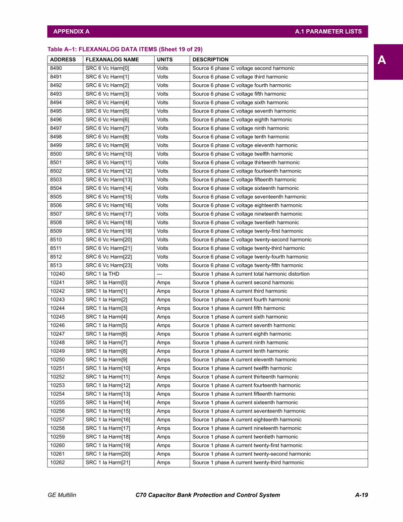
GE Multilin C70 Capacitor Bank Protection and Control System A-19
APPENDIX A A.1 PARAMETER LISTS
A8490 SRC 6 Vc Harm[0] Volts Source 6 phase C voltage second harmonic
8491 SRC 6 Vc Harm[1] Volts Source 6 phase C voltage third harmonic
8492 SRC 6 Vc Harm[2] Volts Source 6 phase C voltage fourth harmonic
8493 SRC 6 Vc Harm[3] Volts Source 6 phase C voltage fifth harmonic
8494 SRC 6 Vc Harm[4] Volts Source 6 phase C voltage sixth harmonic
8495 SRC 6 Vc Harm[5] Volts Source 6 phase C voltage seventh harmonic
8496 SRC 6 Vc Harm[6] Volts Source 6 phase C voltage eighth harmonic
8497 SRC 6 Vc Harm[7] Volts Source 6 phase C voltage ninth harmonic
8498 SRC 6 Vc Harm[8] Volts Source 6 phase C voltage tenth harmonic
8499 SRC 6 Vc Harm[9] Volts Source 6 phase C voltage eleventh harmonic
8500 SRC 6 Vc Harm[10] Volts Source 6 phase C voltage twelfth harmonic
8501 SRC 6 Vc Harm[11] Volts Source 6 phase C voltage thirteenth harmonic
8502 SRC 6 Vc Harm[12] Volts Source 6 phase C voltage fourteenth harmonic
8503 SRC 6 Vc Harm[13] Volts Source 6 phase C voltage fifteenth harmonic
8504 SRC 6 Vc Harm[14] Volts Source 6 phase C voltage sixteenth harmonic
8505 SRC 6 Vc Harm[15] Volts Source 6 phase C voltage seventeenth harmonic
8506 SRC 6 Vc Harm[16] Volts Source 6 phase C voltage eighteenth harmonic
8507 SRC 6 Vc Harm[17] Volts Source 6 phase C voltage nineteenth harmonic
8508 SRC 6 Vc Harm[18] Volts Source 6 phase C voltage twentieth harmonic
8509 SRC 6 Vc Harm[19] Volts Source 6 phase C voltage twenty-first harmonic
8510 SRC 6 Vc Harm[20] Volts Source 6 phase C voltage twenty-second harmonic
8511 SRC 6 Vc Harm[21] Volts Source 6 phase C voltage twenty-third harmonic
8512 SRC 6 Vc Harm[22] Volts Source 6 phase C voltage twenty-fourth harmonic
8513 SRC 6 Vc Harm[23] Volts Source 6 phase C voltage twenty-fifth harmonic
10240 SRC 1 Ia THD --- Source 1 phase A current total harmonic distortion
10241 SRC 1 Ia Harm[0] Amps Source 1 phase A current second harmonic
10242 SRC 1 Ia Harm[1] Amps Source 1 phase A current third harmonic
10243 SRC 1 Ia Harm[2] Amps Source 1 phase A current fourth harmonic
10244 SRC 1 Ia Harm[3] Amps Source 1 phase A current fifth harmonic
10245 SRC 1 Ia Harm[4] Amps Source 1 phase A current sixth harmonic
10246 SRC 1 Ia Harm[5] Amps Source 1 phase A current seventh harmonic
10247 SRC 1 Ia Harm[6] Amps Source 1 phase A current eighth harmonic
10248 SRC 1 Ia Harm[7] Amps Source 1 phase A current ninth harmonic
10249 SRC 1 Ia Harm[8] Amps Source 1 phase A current tenth harmonic
10250 SRC 1 Ia Harm[9] Amps Source 1 phase A current eleventh harmonic
10251 SRC 1 Ia Harm[10] Amps Source 1 phase A current twelfth harmonic
10252 SRC 1 Ia Harm[11] Amps Source 1 phase A current thirteenth harmonic
10253 SRC 1 Ia Harm[12] Amps Source 1 phase A current fourteenth harmonic
10254 SRC 1 Ia Harm[13] Amps Source 1 phase A current fifteenth harmonic
10255 SRC 1 Ia Harm[14] Amps Source 1 phase A current sixteenth harmonic
10256 SRC 1 Ia Harm[15] Amps Source 1 phase A current seventeenth harmonic
10257 SRC 1 Ia Harm[16] Amps Source 1 phase A current eighteenth harmonic
10258 SRC 1 Ia Harm[17] Amps Source 1 phase A current nineteenth harmonic
10259 SRC 1 Ia Harm[18] Amps Source 1 phase A current twentieth harmonic
10260 SRC 1 Ia Harm[19] Amps Source 1 phase A current twenty-first harmonic
10261 SRC 1 Ia Harm[20] Amps Source 1 phase A current twenty-second harmonic
10262 SRC 1 Ia Harm[21] Amps Source 1 phase A current twenty-third harmonic
Table A–1: FLEXANALOG DATA ITEMS (Sheet 19 of 29)
ADDRESS FLEXANALOG NAME UNITS DESCRIPTION
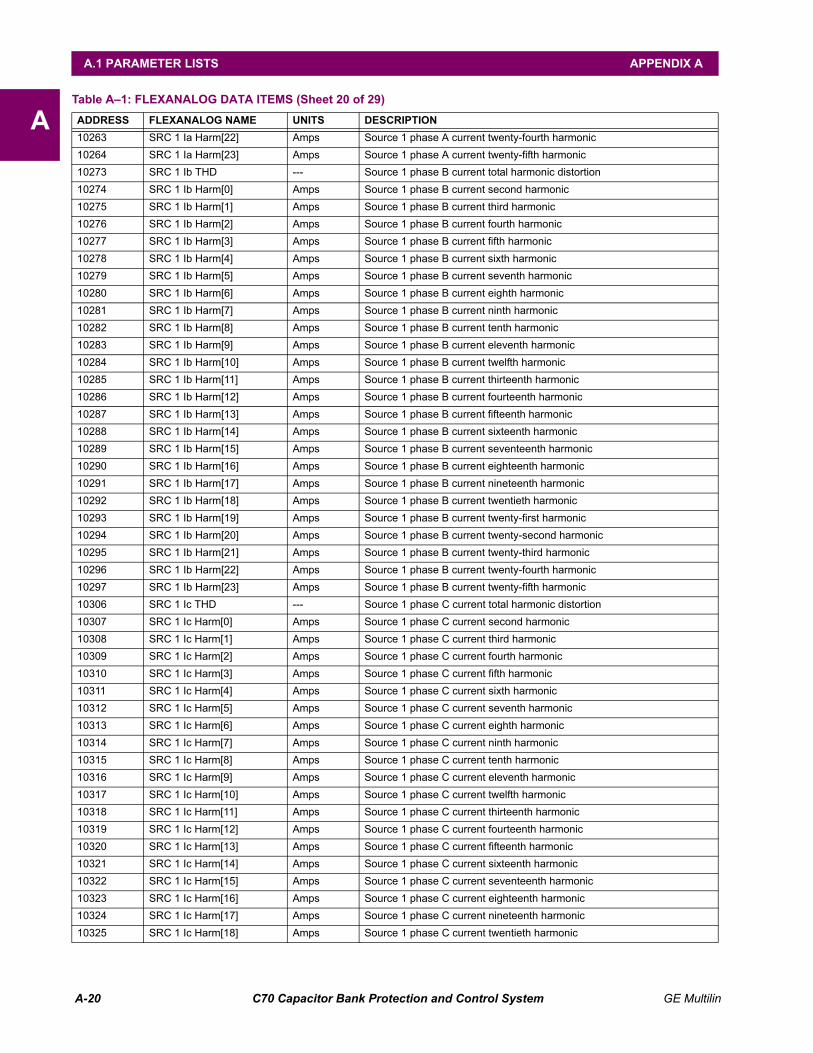
A-20 C70 Capacitor Bank Protection and Control System GE Multilin
A.1 PARAMETER LISTS APPENDIX A
A10263 SRC 1 Ia Harm[22] Amps Source 1 phase A current twenty-fourth harmonic
10264 SRC 1 Ia Harm[23] Amps Source 1 phase A current twenty-fifth harmonic
10273 SRC 1 Ib THD --- Source 1 phase B current total harmonic distortion
10274 SRC 1 Ib Harm[0] Amps Source 1 phase B current second harmonic
10275 SRC 1 Ib Harm[1] Amps Source 1 phase B current third harmonic
10276 SRC 1 Ib Harm[2] Amps Source 1 phase B current fourth harmonic
10277 SRC 1 Ib Harm[3] Amps Source 1 phase B current fifth harmonic
10278 SRC 1 Ib Harm[4] Amps Source 1 phase B current sixth harmonic
10279 SRC 1 Ib Harm[5] Amps Source 1 phase B current seventh harmonic
10280 SRC 1 Ib Harm[6] Amps Source 1 phase B current eighth harmonic
10281 SRC 1 Ib Harm[7] Amps Source 1 phase B current ninth harmonic
10282 SRC 1 Ib Harm[8] Amps Source 1 phase B current tenth harmonic
10283 SRC 1 Ib Harm[9] Amps Source 1 phase B current eleventh harmonic
10284 SRC 1 Ib Harm[10] Amps Source 1 phase B current twelfth harmonic
10285 SRC 1 Ib Harm[11] Amps Source 1 phase B current thirteenth harmonic
10286 SRC 1 Ib Harm[12] Amps Source 1 phase B current fourteenth harmonic
10287 SRC 1 Ib Harm[13] Amps Source 1 phase B current fifteenth harmonic
10288 SRC 1 Ib Harm[14] Amps Source 1 phase B current sixteenth harmonic
10289 SRC 1 Ib Harm[15] Amps Source 1 phase B current seventeenth harmonic
10290 SRC 1 Ib Harm[16] Amps Source 1 phase B current eighteenth harmonic
10291 SRC 1 Ib Harm[17] Amps Source 1 phase B current nineteenth harmonic
10292 SRC 1 Ib Harm[18] Amps Source 1 phase B current twentieth harmonic
10293 SRC 1 Ib Harm[19] Amps Source 1 phase B current twenty-first harmonic
10294 SRC 1 Ib Harm[20] Amps Source 1 phase B current twenty-second harmonic
10295 SRC 1 Ib Harm[21] Amps Source 1 phase B current twenty-third harmonic
10296 SRC 1 Ib Harm[22] Amps Source 1 phase B current twenty-fourth harmonic
10297 SRC 1 Ib Harm[23] Amps Source 1 phase B current twenty-fifth harmonic
10306 SRC 1 Ic THD --- Source 1 phase C current total harmonic distortion
10307 SRC 1 Ic Harm[0] Amps Source 1 phase C current second harmonic
10308 SRC 1 Ic Harm[1] Amps Source 1 phase C current third harmonic
10309 SRC 1 Ic Harm[2] Amps Source 1 phase C current fourth harmonic
10310 SRC 1 Ic Harm[3] Amps Source 1 phase C current fifth harmonic
10311 SRC 1 Ic Harm[4] Amps Source 1 phase C current sixth harmonic
10312 SRC 1 Ic Harm[5] Amps Source 1 phase C current seventh harmonic
10313 SRC 1 Ic Harm[6] Amps Source 1 phase C current eighth harmonic
10314 SRC 1 Ic Harm[7] Amps Source 1 phase C current ninth harmonic
10315 SRC 1 Ic Harm[8] Amps Source 1 phase C current tenth harmonic
10316 SRC 1 Ic Harm[9] Amps Source 1 phase C current eleventh harmonic
10317 SRC 1 Ic Harm[10] Amps Source 1 phase C current twelfth harmonic
10318 SRC 1 Ic Harm[11] Amps Source 1 phase C current thirteenth harmonic
10319 SRC 1 Ic Harm[12] Amps Source 1 phase C current fourteenth harmonic
10320 SRC 1 Ic Harm[13] Amps Source 1 phase C current fifteenth harmonic
10321 SRC 1 Ic Harm[14] Amps Source 1 phase C current sixteenth harmonic
10322 SRC 1 Ic Harm[15] Amps Source 1 phase C current seventeenth harmonic
10323 SRC 1 Ic Harm[16] Amps Source 1 phase C current eighteenth harmonic
10324 SRC 1 Ic Harm[17] Amps Source 1 phase C current nineteenth harmonic
10325 SRC 1 Ic Harm[18] Amps Source 1 phase C current twentieth harmonic
Table A–1: FLEXANALOG DATA ITEMS (Sheet 20 of 29)
ADDRESS FLEXANALOG NAME UNITS DESCRIPTION

GE Multilin C70 Capacitor Bank Protection and Control System A-21
APPENDIX A A.1 PARAMETER LISTS
A10326 SRC 1 Ic Harm[19] Amps Source 1 phase C current twenty-first harmonic
10327 SRC 1 Ic Harm[20] Amps Source 1 phase C current twenty-second harmonic
10328 SRC 1 Ic Harm[21] Amps Source 1 phase C current twenty-third harmonic
10329 SRC 1 Ic Harm[22] Amps Source 1 phase C current twenty-fourth harmonic
10330 SRC 1 Ic Harm[23] Amps Source 1 phase C current twenty-fifth harmonic
10339 SRC 2 Ia THD --- Source 2 phase A current total harmonic distortion
10340 SRC 2 Ia Harm[0] Amps Source 2 phase A current second harmonic
10341 SRC 2 Ia Harm[1] Amps Source 2 phase A current third harmonic
10342 SRC 2 Ia Harm[2] Amps Source 2 phase A current fourth harmonic
10343 SRC 2 Ia Harm[3] Amps Source 2 phase A current fifth harmonic
10344 SRC 2 Ia Harm[4] Amps Source 2 phase A current sixth harmonic
10345 SRC 2 Ia Harm[5] Amps Source 2 phase A current seventh harmonic
10346 SRC 2 Ia Harm[6] Amps Source 2 phase A current eighth harmonic
10347 SRC 2 Ia Harm[7] Amps Source 2 phase A current ninth harmonic
10348 SRC 2 Ia Harm[8] Amps Source 2 phase A current tenth harmonic
10349 SRC 2 Ia Harm[9] Amps Source 2 phase A current eleventh harmonic
10350 SRC 2 Ia Harm[10] Amps Source 2 phase A current twelfth harmonic
10351 SRC 2 Ia Harm[11] Amps Source 2 phase A current thirteenth harmonic
10352 SRC 2 Ia Harm[12] Amps Source 2 phase A current fourteenth harmonic
10353 SRC 2 Ia Harm[13] Amps Source 2 phase A current fifteenth harmonic
10354 SRC 2 Ia Harm[14] Amps Source 2 phase A current sixteenth harmonic
10355 SRC 2 Ia Harm[15] Amps Source 2 phase A current seventeenth harmonic
10356 SRC 2 Ia Harm[16] Amps Source 2 phase A current eighteenth harmonic
10357 SRC 2 Ia Harm[17] Amps Source 2 phase A current nineteenth harmonic
10358 SRC 2 Ia Harm[18] Amps Source 2 phase A current twentieth harmonic
10359 SRC 2 Ia Harm[19] Amps Source 2 phase A current twenty-first harmonic
10360 SRC 2 Ia Harm[20] Amps Source 2 phase A current twenty-second harmonic
10361 SRC 2 Ia Harm[21] Amps Source 2 phase A current twenty-third harmonic
10362 SRC 2 Ia Harm[22] Amps Source 2 phase A current twenty-fourth harmonic
10363 SRC 2 Ia Harm[23] Amps Source 2 phase A current twenty-fifth harmonic
10372 SRC 2 Ib THD --- Source 2 phase B current total harmonic distortion
10373 SRC 2 Ib Harm[0] Amps Source 2 phase B current second harmonic
10374 SRC 2 Ib Harm[1] Amps Source 2 phase B current third harmonic
10375 SRC 2 Ib Harm[2] Amps Source 2 phase B current fourth harmonic
10376 SRC 2 Ib Harm[3] Amps Source 2 phase B current fifth harmonic
10377 SRC 2 Ib Harm[4] Amps Source 2 phase B current sixth harmonic
10378 SRC 2 Ib Harm[5] Amps Source 2 phase B current seventh harmonic
10379 SRC 2 Ib Harm[6] Amps Source 2 phase B current eighth harmonic
10380 SRC 2 Ib Harm[7] Amps Source 2 phase B current ninth harmonic
10381 SRC 2 Ib Harm[8] Amps Source 2 phase B current tenth harmonic
10382 SRC 2 Ib Harm[9] Amps Source 2 phase B current eleventh harmonic
10383 SRC 2 Ib Harm[10] Amps Source 2 phase B current twelfth harmonic
10384 SRC 2 Ib Harm[11] Amps Source 2 phase B current thirteenth harmonic
10385 SRC 2 Ib Harm[12] Amps Source 2 phase B current fourteenth harmonic
10386 SRC 2 Ib Harm[13] Amps Source 2 phase B current fifteenth harmonic
10387 SRC 2 Ib Harm[14] Amps Source 2 phase B current sixteenth harmonic
10388 SRC 2 Ib Harm[15] Amps Source 2 phase B current seventeenth harmonic
Table A–1: FLEXANALOG DATA ITEMS (Sheet 21 of 29)
ADDRESS FLEXANALOG NAME UNITS DESCRIPTION

A-22 C70 Capacitor Bank Protection and Control System GE Multilin
A.1 PARAMETER LISTS APPENDIX A
A10389 SRC 2 Ib Harm[16] Amps Source 2 phase B current eighteenth harmonic
10390 SRC 2 Ib Harm[17] Amps Source 2 phase B current nineteenth harmonic
10391 SRC 2 Ib Harm[18] Amps Source 2 phase B current twentieth harmonic
10392 SRC 2 Ib Harm[19] Amps Source 2 phase B current twenty-first harmonic
10393 SRC 2 Ib Harm[20] Amps Source 2 phase B current twenty-second harmonic
10394 SRC 2 Ib Harm[21] Amps Source 2 phase B current twenty-third harmonic
10395 SRC 2 Ib Harm[22] Amps Source 2 phase B current twenty-fourth harmonic
10396 SRC 2 Ib Harm[23] Amps Source 2 phase B current twenty-fifth harmonic
10405 SRC 2 Ic THD --- Source 2 phase C current total harmonic distortion
10406 SRC 2 Ic Harm[0] Amps Source 2 phase C current second harmonic
10407 SRC 2 Ic Harm[1] Amps Source 2 phase C current third harmonic
10408 SRC 2 Ic Harm[2] Amps Source 2 phase C current fourth harmonic
10409 SRC 2 Ic Harm[3] Amps Source 2 phase C current fifth harmonic
10410 SRC 2 Ic Harm[4] Amps Source 2 phase C current sixth harmonic
10411 SRC 2 Ic Harm[5] Amps Source 2 phase C current seventh harmonic
10412 SRC 2 Ic Harm[6] Amps Source 2 phase C current eighth harmonic
10413 SRC 2 Ic Harm[7] Amps Source 2 phase C current ninth harmonic
10414 SRC 2 Ic Harm[8] Amps Source 2 phase C current tenth harmonic
10415 SRC 2 Ic Harm[9] Amps Source 2 phase C current eleventh harmonic
10416 SRC 2 Ic Harm[10] Amps Source 2 phase C current twelfth harmonic
10417 SRC 2 Ic Harm[11] Amps Source 2 phase C current thirteenth harmonic
10418 SRC 2 Ic Harm[12] Amps Source 2 phase C current fourteenth harmonic
10419 SRC 2 Ic Harm[13] Amps Source 2 phase C current fifteenth harmonic
10420 SRC 2 Ic Harm[14] Amps Source 2 phase C current sixteenth harmonic
10421 SRC 2 Ic Harm[15] Amps Source 2 phase C current seventeenth harmonic
10422 SRC 2 Ic Harm[16] Amps Source 2 phase C current eighteenth harmonic
10423 SRC 2 Ic Harm[17] Amps Source 2 phase C current nineteenth harmonic
10424 SRC 2 Ic Harm[18] Amps Source 2 phase C current twentieth harmonic
10425 SRC 2 Ic Harm[19] Amps Source 2 phase C current twenty-first harmonic
10426 SRC 2 Ic Harm[20] Amps Source 2 phase C current twenty-second harmonic
10427 SRC 2 Ic Harm[21] Amps Source 2 phase C current twenty-third harmonic
10428 SRC 2 Ic Harm[22] Amps Source 2 phase C current twenty-fourth harmonic
10429 SRC 2 Ic Harm[23] Amps Source 2 phase C current twenty-fifth harmonic
10438 SRC 3 Ia THD --- Source 3 phase A current total harmonic distortion
10439 SRC 3 Ia Harm[0] Amps Source 3 phase A current second harmonic
10440 SRC 3 Ia Harm[1] Amps Source 3 phase A current third harmonic
10441 SRC 3 Ia Harm[2] Amps Source 3 phase A current fourth harmonic
10442 SRC 3 Ia Harm[3] Amps Source 3 phase A current fifth harmonic
10443 SRC 3 Ia Harm[4] Amps Source 3 phase A current sixth harmonic
10444 SRC 3 Ia Harm[5] Amps Source 3 phase A current seventh harmonic
10445 SRC 3 Ia Harm[6] Amps Source 3 phase A current eighth harmonic
10446 SRC 3 Ia Harm[7] Amps Source 3 phase A current ninth harmonic
10447 SRC 3 Ia Harm[8] Amps Source 3 phase A current tenth harmonic
10448 SRC 3 Ia Harm[9] Amps Source 3 phase A current eleventh harmonic
10449 SRC 3 Ia Harm[10] Amps Source 3 phase A current twelfth harmonic
10450 SRC 3 Ia Harm[11] Amps Source 3 phase A current thirteenth harmonic
10451 SRC 3 Ia Harm[12] Amps Source 3 phase A current fourteenth harmonic
Table A–1: FLEXANALOG DATA ITEMS (Sheet 22 of 29)
ADDRESS FLEXANALOG NAME UNITS DESCRIPTION
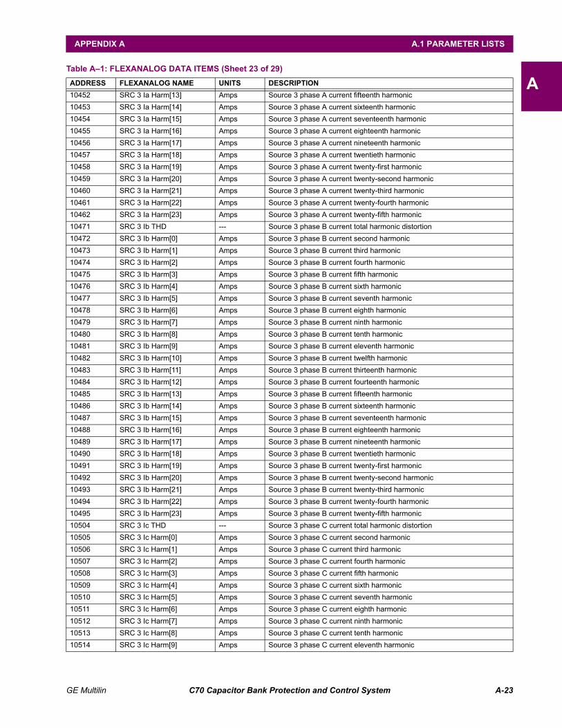
GE Multilin C70 Capacitor Bank Protection and Control System A-23
APPENDIX A A.1 PARAMETER LISTS
A10452 SRC 3 Ia Harm[13] Amps Source 3 phase A current fifteenth harmonic
10453 SRC 3 Ia Harm[14] Amps Source 3 phase A current sixteenth harmonic
10454 SRC 3 Ia Harm[15] Amps Source 3 phase A current seventeenth harmonic
10455 SRC 3 Ia Harm[16] Amps Source 3 phase A current eighteenth harmonic
10456 SRC 3 Ia Harm[17] Amps Source 3 phase A current nineteenth harmonic
10457 SRC 3 Ia Harm[18] Amps Source 3 phase A current twentieth harmonic
10458 SRC 3 Ia Harm[19] Amps Source 3 phase A current twenty-first harmonic
10459 SRC 3 Ia Harm[20] Amps Source 3 phase A current twenty-second harmonic
10460 SRC 3 Ia Harm[21] Amps Source 3 phase A current twenty-third harmonic
10461 SRC 3 Ia Harm[22] Amps Source 3 phase A current twenty-fourth harmonic
10462 SRC 3 Ia Harm[23] Amps Source 3 phase A current twenty-fifth harmonic
10471 SRC 3 Ib THD --- Source 3 phase B current total harmonic distortion
10472 SRC 3 Ib Harm[0] Amps Source 3 phase B current second harmonic
10473 SRC 3 Ib Harm[1] Amps Source 3 phase B current third harmonic
10474 SRC 3 Ib Harm[2] Amps Source 3 phase B current fourth harmonic
10475 SRC 3 Ib Harm[3] Amps Source 3 phase B current fifth harmonic
10476 SRC 3 Ib Harm[4] Amps Source 3 phase B current sixth harmonic
10477 SRC 3 Ib Harm[5] Amps Source 3 phase B current seventh harmonic
10478 SRC 3 Ib Harm[6] Amps Source 3 phase B current eighth harmonic
10479 SRC 3 Ib Harm[7] Amps Source 3 phase B current ninth harmonic
10480 SRC 3 Ib Harm[8] Amps Source 3 phase B current tenth harmonic
10481 SRC 3 Ib Harm[9] Amps Source 3 phase B current eleventh harmonic
10482 SRC 3 Ib Harm[10] Amps Source 3 phase B current twelfth harmonic
10483 SRC 3 Ib Harm[11] Amps Source 3 phase B current thirteenth harmonic
10484 SRC 3 Ib Harm[12] Amps Source 3 phase B current fourteenth harmonic
10485 SRC 3 Ib Harm[13] Amps Source 3 phase B current fifteenth harmonic
10486 SRC 3 Ib Harm[14] Amps Source 3 phase B current sixteenth harmonic
10487 SRC 3 Ib Harm[15] Amps Source 3 phase B current seventeenth harmonic
10488 SRC 3 Ib Harm[16] Amps Source 3 phase B current eighteenth harmonic
10489 SRC 3 Ib Harm[17] Amps Source 3 phase B current nineteenth harmonic
10490 SRC 3 Ib Harm[18] Amps Source 3 phase B current twentieth harmonic
10491 SRC 3 Ib Harm[19] Amps Source 3 phase B current twenty-first harmonic
10492 SRC 3 Ib Harm[20] Amps Source 3 phase B current twenty-second harmonic
10493 SRC 3 Ib Harm[21] Amps Source 3 phase B current twenty-third harmonic
10494 SRC 3 Ib Harm[22] Amps Source 3 phase B current twenty-fourth harmonic
10495 SRC 3 Ib Harm[23] Amps Source 3 phase B current twenty-fifth harmonic
10504 SRC 3 Ic THD --- Source 3 phase C current total harmonic distortion
10505 SRC 3 Ic Harm[0] Amps Source 3 phase C current second harmonic
10506 SRC 3 Ic Harm[1] Amps Source 3 phase C current third harmonic
10507 SRC 3 Ic Harm[2] Amps Source 3 phase C current fourth harmonic
10508 SRC 3 Ic Harm[3] Amps Source 3 phase C current fifth harmonic
10509 SRC 3 Ic Harm[4] Amps Source 3 phase C current sixth harmonic
10510 SRC 3 Ic Harm[5] Amps Source 3 phase C current seventh harmonic
10511 SRC 3 Ic Harm[6] Amps Source 3 phase C current eighth harmonic
10512 SRC 3 Ic Harm[7] Amps Source 3 phase C current ninth harmonic
10513 SRC 3 Ic Harm[8] Amps Source 3 phase C current tenth harmonic
10514 SRC 3 Ic Harm[9] Amps Source 3 phase C current eleventh harmonic
Table A–1: FLEXANALOG DATA ITEMS (Sheet 23 of 29)
ADDRESS FLEXANALOG NAME UNITS DESCRIPTION

A-24 C70 Capacitor Bank Protection and Control System GE Multilin
A.1 PARAMETER LISTS APPENDIX A
A10515 SRC 3 Ic Harm[10] Amps Source 3 phase C current twelfth harmonic
10516 SRC 3 Ic Harm[11] Amps Source 3 phase C current thirteenth harmonic
10517 SRC 3 Ic Harm[12] Amps Source 3 phase C current fourteenth harmonic
10518 SRC 3 Ic Harm[13] Amps Source 3 phase C current fifteenth harmonic
10519 SRC 3 Ic Harm[14] Amps Source 3 phase C current sixteenth harmonic
10520 SRC 3 Ic Harm[15] Amps Source 3 phase C current seventeenth harmonic
10521 SRC 3 Ic Harm[16] Amps Source 3 phase C current eighteenth harmonic
10522 SRC 3 Ic Harm[17] Amps Source 3 phase C current nineteenth harmonic
10523 SRC 3 Ic Harm[18] Amps Source 3 phase C current twentieth harmonic
10524 SRC 3 Ic Harm[19] Amps Source 3 phase C current twenty-first harmonic
10525 SRC 3 Ic Harm[20] Amps Source 3 phase C current twenty-second harmonic
10526 SRC 3 Ic Harm[21] Amps Source 3 phase C current twenty-third harmonic
10527 SRC 3 Ic Harm[22] Amps Source 3 phase C current twenty-fourth harmonic
10528 SRC 3 Ic Harm[23] Amps Source 3 phase C current twenty-fifth harmonic
10537 SRC 4 Ia THD --- Source 4 phase A current total harmonic distortion
10538 SRC 4 Ia Harm[0] Amps Source 4 phase A current second harmonic
10539 SRC 4 Ia Harm[1] Amps Source 4 phase A current third harmonic
10540 SRC 4 Ia Harm[2] Amps Source 4 phase A current fourth harmonic
10541 SRC 4 Ia Harm[3] Amps Source 4 phase A current fifth harmonic
10542 SRC 4 Ia Harm[4] Amps Source 4 phase A current sixth harmonic
10543 SRC 4 Ia Harm[5] Amps Source 4 phase A current seventh harmonic
10544 SRC 4 Ia Harm[6] Amps Source 4 phase A current eighth harmonic
10545 SRC 4 Ia Harm[7] Amps Source 4 phase A current ninth harmonic
10546 SRC 4 Ia Harm[8] Amps Source 4 phase A current tenth harmonic
10547 SRC 4 Ia Harm[9] Amps Source 4 phase A current eleventh harmonic
10548 SRC 4 Ia Harm[10] Amps Source 4 phase A current twelfth harmonic
10549 SRC 4 Ia Harm[11] Amps Source 4 phase A current thirteenth harmonic
10550 SRC 4 Ia Harm[12] Amps Source 4 phase A current fourteenth harmonic
10551 SRC 4 Ia Harm[13] Amps Source 4 phase A current fifteenth harmonic
10552 SRC 4 Ia Harm[14] Amps Source 4 phase A current sixteenth harmonic
10553 SRC 4 Ia Harm[15] Amps Source 4 phase A current seventeenth harmonic
10554 SRC 4 Ia Harm[16] Amps Source 4 phase A current eighteenth harmonic
10555 SRC 4 Ia Harm[17] Amps Source 4 phase A current nineteenth harmonic
10556 SRC 4 Ia Harm[18] Amps Source 4 phase A current twentieth harmonic
10557 SRC 4 Ia Harm[19] Amps Source 4 phase A current twenty-first harmonic
10558 SRC 4 Ia Harm[20] Amps Source 4 phase A current twenty-second harmonic
10559 SRC 4 Ia Harm[21] Amps Source 4 phase A current twenty-third harmonic
10560 SRC 4 Ia Harm[22] Amps Source 4 phase A current twenty-fourth harmonic
10561 SRC 4 Ia Harm[23] Amps Source 4 phase A current twenty-fifth harmonic
10570 SRC 4 Ib THD --- Source 4 phase B current total harmonic distortion
10571 SRC 4 Ib Harm[0] Amps Source 4 phase B current second harmonic
10572 SRC 4 Ib Harm[1] Amps Source 4 phase B current third harmonic
10573 SRC 4 Ib Harm[2] Amps Source 4 phase B current fourth harmonic
10574 SRC 4 Ib Harm[3] Amps Source 4 phase B current fifth harmonic
10575 SRC 4 Ib Harm[4] Amps Source 4 phase B current sixth harmonic
10576 SRC 4 Ib Harm[5] Amps Source 4 phase B current seventh harmonic
10577 SRC 4 Ib Harm[6] Amps Source 4 phase B current eighth harmonic
Table A–1: FLEXANALOG DATA ITEMS (Sheet 24 of 29)
ADDRESS FLEXANALOG NAME UNITS DESCRIPTION

GE Multilin C70 Capacitor Bank Protection and Control System A-25
APPENDIX A A.1 PARAMETER LISTS
A10578 SRC 4 Ib Harm[7] Amps Source 4 phase B current ninth harmonic
10579 SRC 4 Ib Harm[8] Amps Source 4 phase B current tenth harmonic
10580 SRC 4 Ib Harm[9] Amps Source 4 phase B current eleventh harmonic
10581 SRC 4 Ib Harm[10] Amps Source 4 phase B current twelfth harmonic
10582 SRC 4 Ib Harm[11] Amps Source 4 phase B current thirteenth harmonic
10583 SRC 4 Ib Harm[12] Amps Source 4 phase B current fourteenth harmonic
10584 SRC 4 Ib Harm[13] Amps Source 4 phase B current fifteenth harmonic
10585 SRC 4 Ib Harm[14] Amps Source 4 phase B current sixteenth harmonic
10586 SRC 4 Ib Harm[15] Amps Source 4 phase B current seventeenth harmonic
10587 SRC 4 Ib Harm[16] Amps Source 4 phase B current eighteenth harmonic
10588 SRC 4 Ib Harm[17] Amps Source 4 phase B current nineteenth harmonic
10589 SRC 4 Ib Harm[18] Amps Source 4 phase B current twentieth harmonic
10590 SRC 4 Ib Harm[19] Amps Source 4 phase B current twenty-first harmonic
10591 SRC 4 Ib Harm[20] Amps Source 4 phase B current twenty-second harmonic
10592 SRC 4 Ib Harm[21] Amps Source 4 phase B current twenty-third harmonic
10593 SRC 4 Ib Harm[22] Amps Source 4 phase B current twenty-fourth harmonic
10594 SRC 4 Ib Harm[23] Amps Source 4 phase B current twenty-fifth harmonic
10603 SRC 4 Ic THD --- Source 4 phase C current total harmonic distortion
10604 SRC 4 Ic Harm[0] Amps Source 4 phase C current second harmonic
10605 SRC 4 Ic Harm[1] Amps Source 4 phase C current third harmonic
10606 SRC 4 Ic Harm[2] Amps Source 4 phase C current fourth harmonic
10607 SRC 4 Ic Harm[3] Amps Source 4 phase C current fifth harmonic
10608 SRC 4 Ic Harm[4] Amps Source 4 phase C current sixth harmonic
10609 SRC 4 Ic Harm[5] Amps Source 4 phase C current seventh harmonic
10610 SRC 4 Ic Harm[6] Amps Source 4 phase C current eighth harmonic
10611 SRC 4 Ic Harm[7] Amps Source 4 phase C current ninth harmonic
10612 SRC 4 Ic Harm[8] Amps Source 4 phase C current tenth harmonic
10613 SRC 4 Ic Harm[9] Amps Source 4 phase C current eleventh harmonic
10614 SRC 4 Ic Harm[10] Amps Source 4 phase C current twelfth harmonic
10615 SRC 4 Ic Harm[11] Amps Source 4 phase C current thirteenth harmonic
10616 SRC 4 Ic Harm[12] Amps Source 4 phase C current fourteenth harmonic
10617 SRC 4 Ic Harm[13] Amps Source 4 phase C current fifteenth harmonic
10618 SRC 4 Ic Harm[14] Amps Source 4 phase C current sixteenth harmonic
10619 SRC 4 Ic Harm[15] Amps Source 4 phase C current seventeenth harmonic
10620 SRC 4 Ic Harm[16] Amps Source 4 phase C current eighteenth harmonic
10621 SRC 4 Ic Harm[17] Amps Source 4 phase C current nineteenth harmonic
10622 SRC 4 Ic Harm[18] Amps Source 4 phase C current twentieth harmonic
10623 SRC 4 Ic Harm[19] Amps Source 4 phase C current twenty-first harmonic
10624 SRC 4 Ic Harm[20] Amps Source 4 phase C current twenty-second harmonic
10625 SRC 4 Ic Harm[21] Amps Source 4 phase C current twenty-third harmonic
10626 SRC 4 Ic Harm[22] Amps Source 4 phase C current twenty-fourth harmonic
10627 SRC 4 Ic Harm[23] Amps Source 4 phase C current twenty-fifth harmonic
12306 Oscill Num Triggers --- Oscillography number of triggers
13504 DCMA Inputs 1 Value mA dcmA input 1 actual value
13506 DCMA Inputs 2 Value mA dcmA input 2 actual value
13508 DCMA Inputs 3 Value mA dcmA input 3 actual value
13510 DCMA Inputs 4 Value mA dcmA input 4 actual value
Table A–1: FLEXANALOG DATA ITEMS (Sheet 25 of 29)
ADDRESS FLEXANALOG NAME UNITS DESCRIPTION
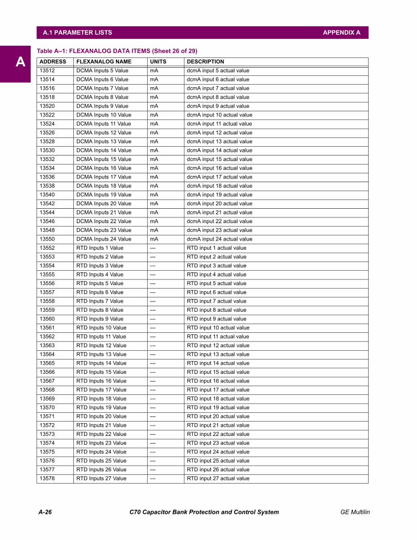
A-26 C70 Capacitor Bank Protection and Control System GE Multilin
A.1 PARAMETER LISTS APPENDIX A
A13512 DCMA Inputs 5 Value mA dcmA input 5 actual value
13514 DCMA Inputs 6 Value mA dcmA input 6 actual value
13516 DCMA Inputs 7 Value mA dcmA input 7 actual value
13518 DCMA Inputs 8 Value mA dcmA input 8 actual value
13520 DCMA Inputs 9 Value mA dcmA input 9 actual value
13522 DCMA Inputs 10 Value mA dcmA input 10 actual value
13524 DCMA Inputs 11 Value mA dcmA input 11 actual value
13526 DCMA Inputs 12 Value mA dcmA input 12 actual value
13528 DCMA Inputs 13 Value mA dcmA input 13 actual value
13530 DCMA Inputs 14 Value mA dcmA input 14 actual value
13532 DCMA Inputs 15 Value mA dcmA input 15 actual value
13534 DCMA Inputs 16 Value mA dcmA input 16 actual value
13536 DCMA Inputs 17 Value mA dcmA input 17 actual value
13538 DCMA Inputs 18 Value mA dcmA input 18 actual value
13540 DCMA Inputs 19 Value mA dcmA input 19 actual value
13542 DCMA Inputs 20 Value mA dcmA input 20 actual value
13544 DCMA Inputs 21 Value mA dcmA input 21 actual value
13546 DCMA Inputs 22 Value mA dcmA input 22 actual value
13548 DCMA Inputs 23 Value mA dcmA input 23 actual value
13550 DCMA Inputs 24 Value mA dcmA input 24 actual value
13552 RTD Inputs 1 Value --- RTD input 1 actual value
13553 RTD Inputs 2 Value --- RTD input 2 actual value
13554 RTD Inputs 3 Value --- RTD input 3 actual value
13555 RTD Inputs 4 Value --- RTD input 4 actual value
13556 RTD Inputs 5 Value --- RTD input 5 actual value
13557 RTD Inputs 6 Value --- RTD input 6 actual value
13558 RTD Inputs 7 Value --- RTD input 7 actual value
13559 RTD Inputs 8 Value --- RTD input 8 actual value
13560 RTD Inputs 9 Value --- RTD input 9 actual value
13561 RTD Inputs 10 Value --- RTD input 10 actual value
13562 RTD Inputs 11 Value --- RTD input 11 actual value
13563 RTD Inputs 12 Value --- RTD input 12 actual value
13564 RTD Inputs 13 Value --- RTD input 13 actual value
13565 RTD Inputs 14 Value --- RTD input 14 actual value
13566 RTD Inputs 15 Value --- RTD input 15 actual value
13567 RTD Inputs 16 Value --- RTD input 16 actual value
13568 RTD Inputs 17 Value --- RTD input 17 actual value
13569 RTD Inputs 18 Value --- RTD input 18 actual value
13570 RTD Inputs 19 Value --- RTD input 19 actual value
13571 RTD Inputs 20 Value --- RTD input 20 actual value
13572 RTD Inputs 21 Value --- RTD input 21 actual value
13573 RTD Inputs 22 Value --- RTD input 22 actual value
13574 RTD Inputs 23 Value --- RTD input 23 actual value
13575 RTD Inputs 24 Value --- RTD input 24 actual value
13576 RTD Inputs 25 Value --- RTD input 25 actual value
13577 RTD Inputs 26 Value --- RTD input 26 actual value
13578 RTD Inputs 27 Value --- RTD input 27 actual value
Table A–1: FLEXANALOG DATA ITEMS (Sheet 26 of 29)
ADDRESS FLEXANALOG NAME UNITS DESCRIPTION

GE Multilin C70 Capacitor Bank Protection and Control System A-27
APPENDIX A A.1 PARAMETER LISTS
A13579 RTD Inputs 28 Value --- RTD input 28 actual value
13580 RTD Inputs 29 Value --- RTD input 29 actual value
13581 RTD Inputs 30 Value --- RTD input 30 actual value
13582 RTD Inputs 31 Value --- RTD input 31 actual value
13583 RTD Inputs 32 Value --- RTD input 32 actual value
13584 RTD Inputs 33 Value --- RTD input 33 actual value
13585 RTD Inputs 34 Value --- RTD input 34 actual value
13586 RTD Inputs 35 Value --- RTD input 35 actual value
13587 RTD Inputs 36 Value --- RTD input 36 actual value
13588 RTD Inputs 37 Value --- RTD input 37 actual value
13589 RTD Inputs 38 Value --- RTD input 38 actual value
13590 RTD Inputs 39 Value --- RTD input 39 actual value
13591 RTD Inputs 40 Value --- RTD input 40 actual value
13592 RTD Inputs 41 Value --- RTD input 41 actual value
13593 RTD Inputs 42 Value --- RTD input 42 actual value
13594 RTD Inputs 43 Value --- RTD input 43 actual value
13595 RTD Inputs 44 Value --- RTD input 44 actual value
13596 RTD Inputs 45 Value --- RTD input 45 actual value
13597 RTD Inputs 46 Value --- RTD input 46 actual value
13598 RTD Inputs 47 Value --- RTD input 47 actual value
13599 RTD Inputs 48 Value --- RTD input 48 actual value
13600 Ohm Inputs 1 Value Ohms Ohm inputs 1 value
13601 Ohm Inputs 2 Value Ohms Ohm inputs 2 value
13824 60P 1 Raw Idiff A Amps Phase current balance raw phase A differential current actual value
13826 60P 1 Raw Idiff B Amps Phase current balance raw phase B differential current actual value
13828 60P 1 Raw Idiff C Amps Phase current balance raw phase C differential current actual value
13830 60P 1 Comp Iop A Amps Phase current balance composite phase A operating current actual value
13832 60P 1 Comp Iop B Amps Phase current balance composite phase B operating current actual value
13834 60P 1 Comp Iop C Amps Phase current balance composite phase C operating current actual value
13888 87V 1 Bus Va Volts Voltage differential 1 phase A bus voltage actual
13890 87V 1 Diff Va Volts Voltage differential 1 phase A diff voltage actual
13892 87V 1 Diff Vb Volts Voltage differential 1 phase B bus voltage actual
13894 87V 1 Diff Vb Volts Voltage differential 1 phase B diff voltage actual
13896 87V 1 Bus Vc Volts Voltage differential 1 phase C bus voltage actual
13898 87V 1 Diff Vc Volts Voltage differential 1 phase C diff voltage actual
13900 87V 2 Bus Va Volts Voltage differential 2 phase A bus voltage actual
13902 87V 2 Diff Va Volts Voltage differential 2 phase A diff voltage actual
13904 87V 2 Bus Vb Volts Voltage differential 2 phase B bus voltage actual
13906 87V 2 Diff Vb Volts Voltage differential 2 phase B diff voltage actual
13908 87V 2 Bus Vc Volts Voltage differential 2 phase C bus voltage actual
13910 87V 2 Diff Vc Volts Voltage differential 2 phase C diff voltage actual
13912 87V 3 Bus Va Volts Voltage differential 3 phase A bus voltage actual
13914 87V 3 Diff Va Volts Voltage differential 3 phase A diff voltage actual
13916 87V 3 Bus Vb Volts Voltage differential 3 phase B buss voltage actual
13918 87V 3 Diff Vb Volts Voltage differential 3 phase B diff voltage actual
13920 87V 3 Bus Vc Volts Voltage differential 3 phase C bus voltage actual
13922 87V 3 Diff Vc Volts Voltage differential 3 phase C diff voltage actual
Table A–1: FLEXANALOG DATA ITEMS (Sheet 27 of 29)
ADDRESS FLEXANALOG NAME UNITS DESCRIPTION
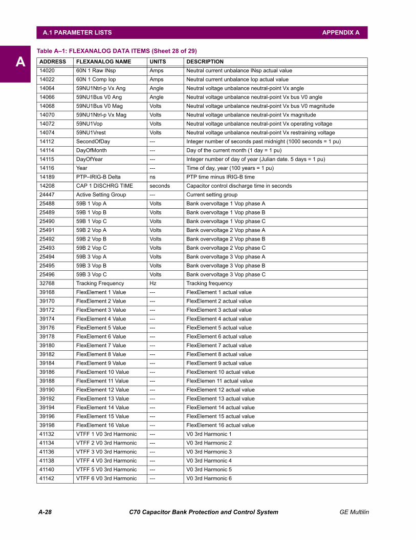
A-28 C70 Capacitor Bank Protection and Control System GE Multilin
A.1 PARAMETER LISTS APPENDIX A
A14020 60N 1 Raw INsp Amps Neutral current unbalance INsp actual value
14022 60N 1 Comp Iop Amps Neutral current unbalance Iop actual value
14064 59NU1Ntrl-p Vx Ang Angle Neutral voltage unbalance neutral-point Vx angle
14066 59NU1Bus V0 Ang Angle Neutral voltage unbalance neutral-point Vx bus V0 angle
14068 59NU1Bus V0 Mag Volts Neutral voltage unbalance neutral-point Vx bus V0 magnitude
14070 59NU1Ntrl-p Vx Mag Volts Neutral voltage unbalance neutral-point Vx magnitude
14072 59NU1Vop Volts Neutral voltage unbalance neutral-point Vx operating voltage
14074 59NU1Vrest Volts Neutral voltage unbalance neutral-point Vx restraining voltage
14112 SecondOfDay --- Integer number of seconds past midnight (1000 seconds = 1 pu)
14114 DayOfMonth --- Day of the current month (1 day = 1 pu)
14115 DayOfYear --- Integer number of day of year (Julian date. 5 days = 1 pu)
14116 Year --- Time of day, year (100 years = 1 pu)
14189 PTP–IRIG-B Delta ns PTP time minus IRIG-B time
14208 CAP 1 DISCHRG TIME seconds Capacitor control discharge time in seconds
24447 Active Setting Group --- Current setting group
25488 59B 1 Vop A Volts Bank overvoltage 1 Vop phase A
25489 59B 1 Vop B Volts Bank overvoltage 1 Vop phase B
25490 59B 1 Vop C Volts Bank overvoltage 1 Vop phase C
25491 59B 2 Vop A Volts Bank overvoltage 2 Vop phase A
25492 59B 2 Vop B Volts Bank overvoltage 2 Vop phase B
25493 59B 2 Vop C Volts Bank overvoltage 2 Vop phase C
25494 59B 3 Vop A Volts Bank overvoltage 3 Vop phase A
25495 59B 3 Vop B Volts Bank overvoltage 3 Vop phase B
25496 59B 3 Vop C Volts Bank overvoltage 3 Vop phase C
32768 Tracking Frequency Hz Tracking frequency
39168 FlexElement 1 Value --- FlexElement 1 actual value
39170 FlexElement 2 Value --- FlexElement 2 actual value
39172 FlexElement 3 Value --- FlexElement 3 actual value
39174 FlexElement 4 Value --- FlexElement 4 actual value
39176 FlexElement 5 Value --- FlexElement 5 actual value
39178 FlexElement 6 Value --- FlexElement 6 actual value
39180 FlexElement 7 Value --- FlexElement 7 actual value
39182 FlexElement 8 Value --- FlexElement 8 actual value
39184 FlexElement 9 Value --- FlexElement 9 actual value
39186 FlexElement 10 Value --- FlexElement 10 actual value
39188 FlexElement 11 Value --- FlexElemen 11 actual value
39190 FlexElement 12 Value --- FlexElement 12 actual value
39192 FlexElement 13 Value --- FlexElement 13 actual value
39194 FlexElement 14 Value --- FlexElement 14 actual value
39196 FlexElement 15 Value --- FlexElement 15 actual value
39198 FlexElement 16 Value --- FlexElement 16 actual value
41132 VTFF 1 V0 3rd Harmonic --- V0 3rd Harmonic 1
41134 VTFF 2 V0 3rd Harmonic --- V0 3rd Harmonic 2
41136 VTFF 3 V0 3rd Harmonic --- V0 3rd Harmonic 3
41138 VTFF 4 V0 3rd Harmonic --- V0 3rd Harmonic 4
41140 VTFF 5 V0 3rd Harmonic --- V0 3rd Harmonic 5
41142 VTFF 6 V0 3rd Harmonic --- V0 3rd Harmonic 6
Table A–1: FLEXANALOG DATA ITEMS (Sheet 28 of 29)
ADDRESS FLEXANALOG NAME UNITS DESCRIPTION

GE Multilin C70 Capacitor Bank Protection and Control System A-29
APPENDIX A A.1 PARAMETER LISTS
A45584 GOOSE Analog In 1 --- IEC 61850 GOOSE analog input 1
45586 GOOSE Analog In 2 --- IEC 61850 GOOSE analog input 2
45588 GOOSE Analog In 3 --- IEC 61850 GOOSE analog input 3
45590 GOOSE Analog In 4 --- IEC 61850 GOOSE analog input 4
45592 GOOSE Analog In 5 --- IEC 61850 GOOSE analog input 5
45594 GOOSE Analog In 6 --- IEC 61850 GOOSE analog input 6
45596 GOOSE Analog In 7 --- IEC 61850 GOOSE analog input 7
45598 GOOSE Analog In 8 --- IEC 61850 GOOSE analog input 8
45600 GOOSE Analog In 9 --- IEC 61850 GOOSE analog input 9
45602 GOOSE Analog In 10 --- IEC 61850 GOOSE analog input 10
45604 GOOSE Analog In 11 --- IEC 61850 GOOSE analog input 11
45606 GOOSE Analog In 12 --- IEC 61850 GOOSE analog input 12
45608 GOOSE Analog In 13 --- IEC 61850 GOOSE analog input 13
45610 GOOSE Analog In 14 --- IEC 61850 GOOSE analog input 14
45612 GOOSE Analog In 15 --- IEC 61850 GOOSE analog input 15
45614 GOOSE Analog In 16 --- IEC 61850 GOOSE analog input 16
Table A–1: FLEXANALOG DATA ITEMS (Sheet 29 of 29)
ADDRESS FLEXANALOG NAME UNITS DESCRIPTION
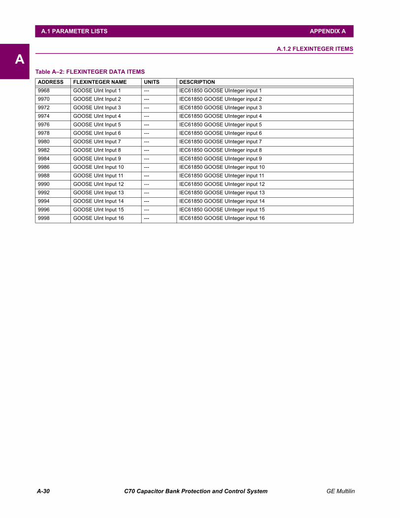
A-30 C70 Capacitor Bank Protection and Control System GE Multilin
A.1 PARAMETER LISTS APPENDIX A
AA.1.2 FLEXINTEGER ITEMS
Table A–2: FLEXINTEGER DATA ITEMS
ADDRESS FLEXINTEGER NAME UNITS DESCRIPTION
9968 GOOSE UInt Input 1 --- IEC61850 GOOSE UInteger input 1
9970 GOOSE UInt Input 2 --- IEC61850 GOOSE UInteger input 2
9972 GOOSE UInt Input 3 --- IEC61850 GOOSE UInteger input 3
9974 GOOSE UInt Input 4 --- IEC61850 GOOSE UInteger input 4
9976 GOOSE UInt Input 5 --- IEC61850 GOOSE UInteger input 5
9978 GOOSE UInt Input 6 --- IEC61850 GOOSE UInteger input 6
9980 GOOSE UInt Input 7 --- IEC61850 GOOSE UInteger input 7
9982 GOOSE UInt Input 8 --- IEC61850 GOOSE UInteger input 8
9984 GOOSE UInt Input 9 --- IEC61850 GOOSE UInteger input 9
9986 GOOSE UInt Input 10 --- IEC61850 GOOSE UInteger input 10
9988 GOOSE UInt Input 11 --- IEC61850 GOOSE UInteger input 11
9990 GOOSE UInt Input 12 --- IEC61850 GOOSE UInteger input 12
9992 GOOSE UInt Input 13 --- IEC61850 GOOSE UInteger input 13
9994 GOOSE UInt Input 14 --- IEC61850 GOOSE UInteger input 14
9996 GOOSE UInt Input 15 --- IEC61850 GOOSE UInteger input 15
9998 GOOSE UInt Input 16 --- IEC61850 GOOSE UInteger input 16

GE Multilin C70 Capacitor Bank Protection and Control System B-1
APPENDIX B B.1 MODBUS RTU PROTOCOL
B
APPENDIX B MODBUS COMMUNICATIONSB.1MODBUS RTU PROTOCOL B.1.1 INTRODUCTION
The UR-series relays support a number of communications protocols to allow connection to equipment such as personalcomputers, RTUs, SCADA masters, and programmable logic controllers. The Modicon Modbus RTU protocol is the mostbasic protocol supported by the UR. Modbus is available via RS232 or RS485 serial links or via ethernet (using the Mod-bus/TCP specification). The following description is intended primarily for users who wish to develop their own master com-munication drivers and applies to the serial Modbus RTU protocol. Note that:
• The UR always acts as a slave device, meaning that it never initiates communications; it only listens and responds torequests issued by a master computer.
• For Modbus, a subset of the Remote Terminal Unit (RTU) protocol format is supported that allows extensive monitor-ing, programming, and control functions using read and write register commands.
B.1.2 PHYSICAL LAYER
The Modbus RTU protocol is hardware-independent so that the physical layer can be any of a variety of standard hardwareconfigurations including RS232 and RS485. The relay includes a faceplate (front panel) RS232 port and two rear terminalcommunications ports that may be configured as RS485, fiber optic, 10Base-T, or 10Base-F. Data flow is half-duplex in allconfigurations. See chapter 3 for details on communications wiring.
Each data byte is transmitted in an asynchronous format consisting of 1 start bit, 8 data bits, 1 stop bit, and possibly 1 paritybit. This produces a 10 or 11 bit data frame. This can be important for transmission through modems at high bit rates (11 bitdata frames are not supported by many modems at baud rates greater than 300).
The baud rate and parity are independently programmable for each communications port. Baud rates of 300, 1200, 2400,4800, 9600, 14400, 19200, 28800, 33600, 38400, 57600, or 115200 bps are available. Even, odd, and no parity are avail-able. Refer to the Communications section of chapter 5 for further details.
The master device in any system must know the address of the slave device with which it is to communicate. The relay willnot act on a request from a master if the address in the request does not match the relay’s slave address (unless theaddress is the broadcast address – see below).
A single setting selects the slave address used for all ports, with the exception that for the faceplate port, the relay willaccept any address when the Modbus RTU protocol is used.
B.1.3 DATA LINK LAYER
Communications takes place in packets which are groups of asynchronously framed byte data. The master transmits apacket to the slave and the slave responds with a packet. The end of a packet is marked by dead-time on the communica-tions line. The following describes general format for both transmit and receive packets. For exact details on packet format-ting, refer to subsequent sections describing each function code.
• SLAVE ADDRESS: This is the address of the slave device that is intended to receive the packet sent by the masterand to perform the desired action. Each slave device on a communications bus must have a unique address to preventbus contention. All of the relay’s ports have the same address which is programmable from 1 to 254; see chapter 5 fordetails. Only the addressed slave will respond to a packet that starts with its address. Note that the faceplate port is anexception to this rule; it will act on a message containing any slave address.
A master transmit packet with slave address 0 indicates a broadcast command. All slaves on the communication linktake action based on the packet, but none respond to the master. Broadcast mode is only recognized when associatedwith function code 05h. For any other function code, a packet with broadcast mode slave address 0 will be ignored.
Table B–1: MODBUS PACKET FORMAT
DESCRIPTION SIZE
SLAVE ADDRESS 1 byte
FUNCTION CODE 1 byte
DATA N bytes
CRC 2 bytes
DEAD TIME 3.5 bytes transmission time

B-2 C70 Capacitor Bank Protection and Control System GE Multilin
B.1 MODBUS RTU PROTOCOL APPENDIX B
B
• FUNCTION CODE: This is one of the supported functions codes of the unit which tells the slave what action to per-form. See the Supported Function Codes section for complete details. An exception response from the slave is indi-cated by setting the high order bit of the function code in the response packet. See the Exception Responses sectionfor further details.
• DATA: This will be a variable number of bytes depending on the function code. This may include actual values, set-tings, or addresses sent by the master to the slave or by the slave to the master.
• CRC: This is a two byte error checking code. The RTU version of Modbus includes a 16-bit cyclic redundancy check(CRC-16) with every packet which is an industry standard method used for error detection. If a Modbus slave devicereceives a packet in which an error is indicated by the CRC, the slave device will not act upon or respond to the packetthus preventing any erroneous operations. See the CRC-16 Algorithm section for details on calculating the CRC.
• DEAD TIME: A packet is terminated when no data is received for a period of 3.5 byte transmission times (about 15 msat 2400 bps, 2 ms at 19200 bps, and 300 µs at 115200 bps). Consequently, the transmitting device must not allow gapsbetween bytes longer than this interval. Once the dead time has expired without a new byte transmission, all slavesstart listening for a new packet from the master except for the addressed slave.
B.1.4 CRC-16 ALGORITHM
The CRC-16 algorithm essentially treats the entire data stream (data bits only; start, stop and parity ignored) as one contin-uous binary number. This number is first shifted left 16 bits and then divided by a characteristic polynomial(11000000000000101B). The 16-bit remainder of the division is appended to the end of the packet, MSByte first. Theresulting packet including CRC, when divided by the same polynomial at the receiver will give a zero remainder if no trans-mission errors have occurred. This algorithm requires the characteristic polynomial to be reverse bit ordered. The most sig-nificant bit of the characteristic polynomial is dropped, since it does not affect the value of the remainder.
A C programming language implementation of the CRC algorithm will be provided upon request.
Table B–2: CRC-16 ALGORITHM
SYMBOLS: --> data transfer
A 16 bit working register
Alow low order byte of A
Ahigh high order byte of A
CRC 16 bit CRC-16 result
i,j loop counters
(+) logical EXCLUSIVE-OR operator
N total number of data bytes
Di i-th data byte (i = 0 to N-1)
G 16 bit characteristic polynomial = 1010000000000001 (binary) with MSbit dropped and bit order reversed
shr (x) right shift operator (th LSbit of x is shifted into a carry flag, a '0' is shifted into the MSbit of x, all other bits are shifted right one location)
ALGORITHM: 1. FFFF (hex) --> A
2. 0 --> i
3. 0 --> j
4. Di (+) Alow --> Alow
5. j + 1 --> j
6. shr (A)
7. Is there a carry? No: go to 8; Yes: G (+) A --> A and continue.
8. Is j = 8? No: go to 5; Yes: continue
9. i + 1 --> i
10. Is i = N? No: go to 3; Yes: continue
11. A --> CRC
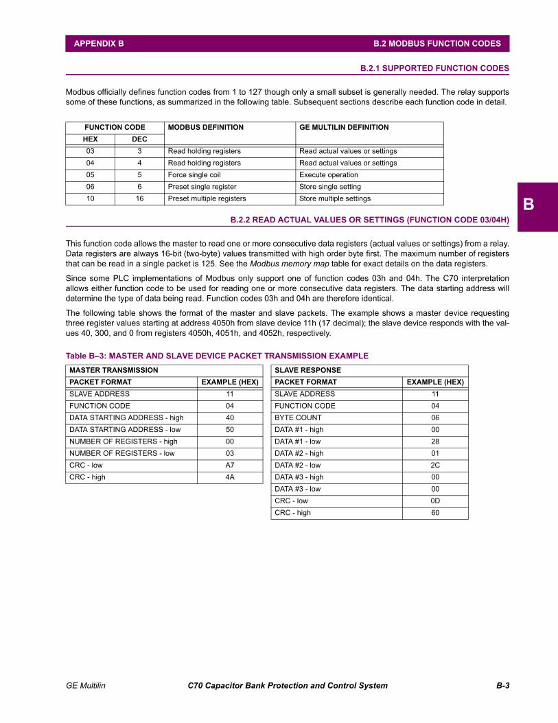
GE Multilin C70 Capacitor Bank Protection and Control System B-3
APPENDIX B B.2 MODBUS FUNCTION CODES
B
B.2MODBUS FUNCTION CODES B.2.1 SUPPORTED FUNCTION CODES
Modbus officially defines function codes from 1 to 127 though only a small subset is generally needed. The relay supportssome of these functions, as summarized in the following table. Subsequent sections describe each function code in detail.
B.2.2 READ ACTUAL VALUES OR SETTINGS (FUNCTION CODE 03/04H)
This function code allows the master to read one or more consecutive data registers (actual values or settings) from a relay.Data registers are always 16-bit (two-byte) values transmitted with high order byte first. The maximum number of registersthat can be read in a single packet is 125. See the Modbus memory map table for exact details on the data registers.
Since some PLC implementations of Modbus only support one of function codes 03h and 04h. The C70 interpretationallows either function code to be used for reading one or more consecutive data registers. The data starting address willdetermine the type of data being read. Function codes 03h and 04h are therefore identical.
The following table shows the format of the master and slave packets. The example shows a master device requestingthree register values starting at address 4050h from slave device 11h (17 decimal); the slave device responds with the val-ues 40, 300, and 0 from registers 4050h, 4051h, and 4052h, respectively.
FUNCTION CODE MODBUS DEFINITION GE MULTILIN DEFINITION
HEX DEC
03 3 Read holding registers Read actual values or settings
04 4 Read holding registers Read actual values or settings
05 5 Force single coil Execute operation
06 6 Preset single register Store single setting
10 16 Preset multiple registers Store multiple settings
Table B–3: MASTER AND SLAVE DEVICE PACKET TRANSMISSION EXAMPLE
MASTER TRANSMISSION SLAVE RESPONSE
PACKET FORMAT EXAMPLE (HEX) PACKET FORMAT EXAMPLE (HEX)
SLAVE ADDRESS 11 SLAVE ADDRESS 11
FUNCTION CODE 04 FUNCTION CODE 04
DATA STARTING ADDRESS - high 40 BYTE COUNT 06
DATA STARTING ADDRESS - low 50 DATA #1 - high 00
NUMBER OF REGISTERS - high 00 DATA #1 - low 28
NUMBER OF REGISTERS - low 03 DATA #2 - high 01
CRC - low A7 DATA #2 - low 2C
CRC - high 4A DATA #3 - high 00
DATA #3 - low 00
CRC - low 0D
CRC - high 60
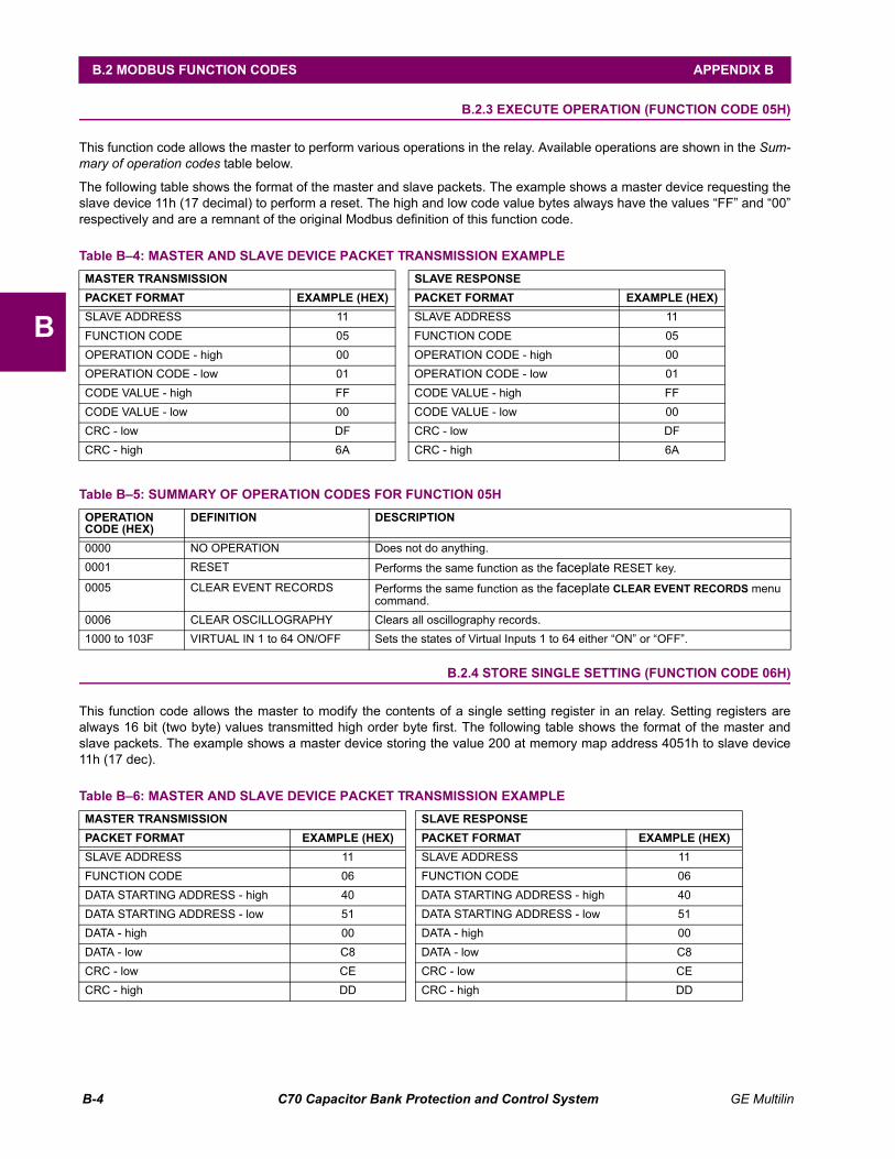
B-4 C70 Capacitor Bank Protection and Control System GE Multilin
B.2 MODBUS FUNCTION CODES APPENDIX B
B
B.2.3 EXECUTE OPERATION (FUNCTION CODE 05H)
This function code allows the master to perform various operations in the relay. Available operations are shown in the Sum-mary of operation codes table below.
The following table shows the format of the master and slave packets. The example shows a master device requesting theslave device 11h (17 decimal) to perform a reset. The high and low code value bytes always have the values “FF” and “00”respectively and are a remnant of the original Modbus definition of this function code.
B.2.4 STORE SINGLE SETTING (FUNCTION CODE 06H)
This function code allows the master to modify the contents of a single setting register in an relay. Setting registers arealways 16 bit (two byte) values transmitted high order byte first. The following table shows the format of the master andslave packets. The example shows a master device storing the value 200 at memory map address 4051h to slave device11h (17 dec).
Table B–4: MASTER AND SLAVE DEVICE PACKET TRANSMISSION EXAMPLE
MASTER TRANSMISSION SLAVE RESPONSE
PACKET FORMAT EXAMPLE (HEX) PACKET FORMAT EXAMPLE (HEX)
SLAVE ADDRESS 11 SLAVE ADDRESS 11
FUNCTION CODE 05 FUNCTION CODE 05
OPERATION CODE - high 00 OPERATION CODE - high 00
OPERATION CODE - low 01 OPERATION CODE - low 01
CODE VALUE - high FF CODE VALUE - high FF
CODE VALUE - low 00 CODE VALUE - low 00
CRC - low DF CRC - low DF
CRC - high 6A CRC - high 6A
Table B–5: SUMMARY OF OPERATION CODES FOR FUNCTION 05H
OPERATION CODE (HEX)
DEFINITION DESCRIPTION
0000 NO OPERATION Does not do anything.
0001 RESET Performs the same function as the faceplate RESET key.
0005 CLEAR EVENT RECORDS Performs the same function as the faceplate CLEAR EVENT RECORDS menu command.
0006 CLEAR OSCILLOGRAPHY Clears all oscillography records.
1000 to 103F VIRTUAL IN 1 to 64 ON/OFF Sets the states of Virtual Inputs 1 to 64 either “ON” or “OFF”.
Table B–6: MASTER AND SLAVE DEVICE PACKET TRANSMISSION EXAMPLE
MASTER TRANSMISSION SLAVE RESPONSE
PACKET FORMAT EXAMPLE (HEX) PACKET FORMAT EXAMPLE (HEX)
SLAVE ADDRESS 11 SLAVE ADDRESS 11
FUNCTION CODE 06 FUNCTION CODE 06
DATA STARTING ADDRESS - high 40 DATA STARTING ADDRESS - high 40
DATA STARTING ADDRESS - low 51 DATA STARTING ADDRESS - low 51
DATA - high 00 DATA - high 00
DATA - low C8 DATA - low C8
CRC - low CE CRC - low CE
CRC - high DD CRC - high DD

GE Multilin C70 Capacitor Bank Protection and Control System B-5
APPENDIX B B.2 MODBUS FUNCTION CODES
B
B.2.5 STORE MULTIPLE SETTINGS (FUNCTION CODE 10H)
This function code allows the master to modify the contents of a one or more consecutive setting registers in a relay. Settingregisters are 16-bit (two byte) values transmitted high order byte first. The maximum number of setting registers that can bestored in a single packet is 60. The following table shows the format of the master and slave packets. The example showsa master device storing the value 200 at memory map address 4051h, and the value 1 at memory map address 4052h toslave device 11h (17 decimal).
B.2.6 EXCEPTION RESPONSES
Programming or operation errors usually happen because of illegal data in a packet. These errors result in an exceptionresponse from the slave. The slave detecting one of these errors sends a response packet to the master with the high orderbit of the function code set to 1.
The following table shows the format of the master and slave packets. The example shows a master device sending theunsupported function code 39h to slave device 11.
Table B–7: MASTER AND SLAVE DEVICE PACKET TRANSMISSION EXAMPLE
MASTER TRANSMISSION SLAVE RESPONSE
PACKET FORMAT EXAMPLE (HEX) PACKET FORMAT EXAMPLE (HEX)
SLAVE ADDRESS 11 SLAVE ADDRESS 11
FUNCTION CODE 10 FUNCTION CODE 10
DATA STARTING ADDRESS - hi 40 DATA STARTING ADDRESS - hi 40
DATA STARTING ADDRESS - lo 51 DATA STARTING ADDRESS - lo 51
NUMBER OF SETTINGS - hi 00 NUMBER OF SETTINGS - hi 00
NUMBER OF SETTINGS - lo 02 NUMBER OF SETTINGS - lo 02
BYTE COUNT 04 CRC - lo 07
DATA #1 - high order byte 00 CRC - hi 64
DATA #1 - low order byte C8
DATA #2 - high order byte 00
DATA #2 - low order byte 01
CRC - low order byte 12
CRC - high order byte 62
Table B–8: MASTER AND SLAVE DEVICE PACKET TRANSMISSION EXAMPLE
MASTER TRANSMISSION SLAVE RESPONSE
PACKET FORMAT EXAMPLE (HEX) PACKET FORMAT EXAMPLE (HEX)
SLAVE ADDRESS 11 SLAVE ADDRESS 11
FUNCTION CODE 39 FUNCTION CODE B9
CRC - low order byte CD ERROR CODE 01
CRC - high order byte F2 CRC - low order byte 93
CRC - high order byte 95

B-6 C70 Capacitor Bank Protection and Control System GE Multilin
B.3 FILE TRANSFERS APPENDIX B
B
B.3FILE TRANSFERS B.3.1 OBTAINING RELAY FILES VIA MODBUS
a) DESCRIPTION
The UR relay has a generic file transfer facility, meaning that you use the same method to obtain all of the different types offiles from the unit. The Modbus registers that implement file transfer are found in the "Modbus File Transfer (Read/Write)"and "Modbus File Transfer (Read Only)" modules, starting at address 3100 in the Modbus Memory Map. To read a file fromthe UR relay, use the following steps:
1. Write the filename to the "Name of file to read" register using a write multiple registers command. If the name is shorterthan 80 characters, you may write only enough registers to include all the text of the filename. Filenames are not casesensitive.
2. Repeatedly read all the registers in "Modbus File Transfer (Read Only)" using a read multiple registers command. It isnot necessary to read the entire data block, since the UR relay will remember which was the last register you read. The"position" register is initially zero and thereafter indicates how many bytes (2 times the number of registers) you haveread so far. The "size of..." register indicates the number of bytes of data remaining to read, to a maximum of 244.
3. Keep reading until the "size of..." register is smaller than the number of bytes you are transferring. This condition indi-cates end of file. Discard any bytes you have read beyond the indicated block size.
4. If you need to re-try a block, read only the "size of.." and "block of data", without reading the position. The file pointer isonly incremented when you read the position register, so the same data block will be returned as was read in the pre-vious operation. On the next read, check to see if the position is where you expect it to be, and discard the previousblock if it is not (this condition would indicate that the UR relay did not process your original read request).
The UR relay retains connection-specific file transfer information, so files may be read simultaneously on multiple Modbusconnections.
b) OTHER PROTOCOLS
All the files available via Modbus may also be retrieved using the standard file transfer mechanisms in other protocols (forexample, TFTP or MMS).
c) COMTRADE, OSCILLOGRAPHY, AND DATA LOGGER FILES
Oscillography and data logger files are formatted using the COMTRADE file format per IEEE C37.111-1999 Standard Com-mon Format for Transient Data Exchange (COMTRADE) for Power Systems. The files can be obtained in either text orbinary COMTRADE format.
d) READING OSCILLOGRAPHY FILES
Familiarity with the oscillography feature is required to understand the following description. Refer to the Oscillography sec-tion in Chapter 5 for additional details.
The Oscillography Number of Triggers register is incremented by one every time a new oscillography file is triggered (cap-tured) and cleared to zero when oscillography data is cleared. When a new trigger occurs, the associated oscillography fileis assigned a file identifier number equal to the incremented value of this register; the newest file number is equal to theOscillography_Number_of_Triggers register. This register can be used to determine if any new data has been captured byperiodically reading it to see if the value has changed; if the number has increased then new data is available.
The Oscillography Number of Records register specifies the maximum number of files (and the number of cycles of dataper file) that can be stored in memory of the relay. The Oscillography Available Records register specifies the actual num-ber of files that are stored and still available to be read out of the relay.
Writing “Yes” (i.e. the value 1) to the Oscillography Clear Data register clears oscillography data files, clears both the Oscil-lography Number of Triggers and Oscillography Available Records registers to zero, and sets the Oscillography LastCleared Date to the present date and time.
To read binary COMTRADE oscillography files, read the following filenames:
OSCnnnn.CFG and OSCnnn.DAT
e) READING DATA LOGGER FILES
Familiarity with the data logger feature is required to understand this description. Refer to the Data Logger section of Chap-ter 5 for details. To read the entire data logger in binary COMTRADE format, read the following files.

GE Multilin C70 Capacitor Bank Protection and Control System B-7
APPENDIX B B.3 FILE TRANSFERS
B
datalog.cfg and datalog.dat
To read the entire data logger in ASCII COMTRADE format, read the following files.
dataloga.cfg and dataloga.dat
To limit the range of records to be returned in the COMTRADE files, append the following to the filename before writing it:
• To read from a specific time to the end of the log: <space> startTime
• To read a specific range of records: <space> startTime <space> endTime
• Replace <startTime> and <endTime> with Julian dates (seconds since Jan. 1 1970) as numeric text.
f) READING EVENT RECORDER FILES
To read the entire event recorder contents in ASCII format (the only available format), use the following filename:
EVT.TXT
To read from a specific record to the end of the log, use the following filename:
EVTnnn.TXT (replace nnn with the desired starting record number)
To read from a specific record to another specific record, use the following filename:
EVT.TXT xxxxx yyyyy (replace xxxxx with the starting record number and yyyyy with the ending record number)
B.3.2 MODBUS PASSWORD OPERATION
The C70 supports password entry from a local or remote connection.
Local access is defined as any access to settings or commands via the faceplate interface. This includes both keypad entryand the faceplate RS232 connection. Remote access is defined as any access to settings or commands via any rear com-munications port. This includes both Ethernet and RS485 connections. Any changes to the local or remote passwordsenables this functionality.
When entering a settings or command password via EnerVista or any serial interface, the user must enter the correspond-ing connection password. If the connection is to the back of the C70, the remote password must be used. If the connectionis to the RS232 port of the faceplate, the local password must be used.
The command password is set up at memory location 4000. Storing a value of “0” removes command password protection.When reading the password setting, the encrypted value (zero if no password is set) is returned. Command security isrequired to change the command password. Similarly, the setting password is set up at memory location 4002. These arethe same settings and encrypted values found in the SETTINGS PRODUCT SETUP PASSWORD SECURITY menu via thekeypad. Enabling password security for the faceplate display will also enable it for Modbus, and vice-versa.
To gain command level security access, the command password must be entered at memory location 4008. To gain settinglevel security access, the setting password must be entered at memory location 400A. The entered setting password mustmatch the current setting password setting, or must be zero, to change settings or download firmware.
Command and setting passwords each have a 30 minute timer. Each timer starts when you enter the particular password,and is re-started whenever you use it. For example, writing a setting re-starts the setting password timer and writing a com-mand register or forcing a coil re-starts the command password timer. The value read at memory location 4010 can be usedto confirm whether a command password is enabled or disabled (a value of 0 represents disabled). The value read at mem-ory location 4011 can be used to confirm whether a setting password is enabled or disabled.
Command or setting password security access is restricted to the particular port or particular TCP/IP connection on whichthe entry was made. Passwords must be entered when accessing the relay through other ports or connections, and thepasswords must be re-entered after disconnecting and re-connecting on TCP/IP.

B-8 C70 Capacitor Bank Protection and Control System GE Multilin
B.4 MEMORY MAPPING APPENDIX B
B
B.4MEMORY MAPPING B.4.1 MODBUS MEMORY MAP
Table B–9: MODBUS MEMORY MAP (Sheet 1 of 61)
ADDR REGISTER NAME RANGE UNITS STEP FORMAT DEFAULT
Product Information (Read Only)
0000 UR Product Type 0 to 65535 --- 1 F001 0
0002 Product Version 0 to 655.35 --- 0.01 F001 1
0003 Boot Configuration Register 0 to 65535 --- 1 F001 0
Product Information (Read Only -- Written by Factory)
0010 Serial Number --- --- --- F203 “0”
0020 Manufacturing Date 0 to 4294967295 --- 1 F050 0
0022 Modification Number 0 to 65535 --- 1 F001 0
0040 Order Code --- --- --- F204 “Order Code x”
0090 Ethernet MAC Address --- --- --- F072 0
0093 Reserved (13 items) --- --- --- F001 0
00A0 CPU Module Serial Number --- --- --- F203 (none)
00B0 CPU Supplier Serial Number --- --- --- F203 (none)
00C0 Ethernet Sub Module Serial Number (8 items) --- --- --- F203 (none)
Product Information (Read Only -- Written by Factory)
0110 FPGA Version --- --- --- F206 (none)
0113 FPGA Date 0 to 4294967295 -- 1 F050 0
Self Test Targets (Read Only)
0200 Self Test States (4 items) 0 to 4294967295 0 1 F143 0
Front Panel (Read Only)
0208 LED Column n State, n = 1 to 10 (10 items) 0 to 65535 --- 1 F501 0
0220 Display Message --- --- --- F204 (none)
0248 Last Key Pressed 0 to 47 --- 1 F530 0 (None)
Keypress Emulation (Read/Write)
0280 Simulated keypress -- write zero before each keystroke 0 to 46 --- 1 F190 0 (No key -- use between real
keys)
Virtual Input Commands (Read/Write Command) (64 modules)
0400 Virtual Input 1 State 0 to 1 --- 1 F108 0 (Off)
0401 Virtual Input 2 State 0 to 1 --- 1 F108 0 (Off)
0402 Virtual Input 3 State 0 to 1 --- 1 F108 0 (Off)
0403 Virtual Input 4 State 0 to 1 --- 1 F108 0 (Off)
0404 Virtual Input 5 State 0 to 1 --- 1 F108 0 (Off)
0405 Virtual Input 6 State 0 to 1 --- 1 F108 0 (Off)
0406 Virtual Input 7 State 0 to 1 --- 1 F108 0 (Off)
0407 Virtual Input 8 State 0 to 1 --- 1 F108 0 (Off)
0408 Virtual Input 9 State 0 to 1 --- 1 F108 0 (Off)
0409 Virtual Input 10 State 0 to 1 --- 1 F108 0 (Off)
040A Virtual Input 11 State 0 to 1 --- 1 F108 0 (Off)
040B Virtual Input 12 State 0 to 1 --- 1 F108 0 (Off)
040C Virtual Input 13 State 0 to 1 --- 1 F108 0 (Off)
040D Virtual Input 14 State 0 to 1 --- 1 F108 0 (Off)
040E Virtual Input 15 State 0 to 1 --- 1 F108 0 (Off)
040F Virtual Input 16 State 0 to 1 --- 1 F108 0 (Off)
0410 Virtual Input 17 State 0 to 1 --- 1 F108 0 (Off)
0411 Virtual Input 18 State 0 to 1 --- 1 F108 0 (Off)
0412 Virtual Input 19 State 0 to 1 --- 1 F108 0 (Off)
0413 Virtual Input 20 State 0 to 1 --- 1 F108 0 (Off)
0414 Virtual Input 21 State 0 to 1 --- 1 F108 0 (Off)
0415 Virtual Input 22 State 0 to 1 --- 1 F108 0 (Off)
0416 Virtual Input 23 State 0 to 1 --- 1 F108 0 (Off)

GE Multilin C70 Capacitor Bank Protection and Control System B-9
APPENDIX B B.4 MEMORY MAPPING
B
0417 Virtual Input 24 State 0 to 1 --- 1 F108 0 (Off)
0418 Virtual Input 25 State 0 to 1 --- 1 F108 0 (Off)
0419 Virtual Input 26 State 0 to 1 --- 1 F108 0 (Off)
041A Virtual Input 27 State 0 to 1 --- 1 F108 0 (Off)
041B Virtual Input 28 State 0 to 1 --- 1 F108 0 (Off)
041C Virtual Input 29 State 0 to 1 --- 1 F108 0 (Off)
041D Virtual Input 30 State 0 to 1 --- 1 F108 0 (Off)
041E Virtual Input 31 State 0 to 1 --- 1 F108 0 (Off)
041F Virtual Input 32 State 0 to 1 --- 1 F108 0 (Off)
0420 Virtual Input 33 State 0 to 1 --- 1 F108 0 (Off)
0421 Virtual Input 34 State 0 to 1 --- 1 F108 0 (Off)
0422 Virtual Input 35 State 0 to 1 --- 1 F108 0 (Off)
0423 Virtual Input 36 State 0 to 1 --- 1 F108 0 (Off)
0424 Virtual Input 37 State 0 to 1 --- 1 F108 0 (Off)
0425 Virtual Input 38 State 0 to 1 --- 1 F108 0 (Off)
0426 Virtual Input 39 State 0 to 1 --- 1 F108 0 (Off)
0427 Virtual Input 40 State 0 to 1 --- 1 F108 0 (Off)
0428 Virtual Input 41 State 0 to 1 --- 1 F108 0 (Off)
0429 Virtual Input 42 State 0 to 1 --- 1 F108 0 (Off)
042A Virtual Input 43 State 0 to 1 --- 1 F108 0 (Off)
042B Virtual Input 44 State 0 to 1 --- 1 F108 0 (Off)
042C Virtual Input 45 State 0 to 1 --- 1 F108 0 (Off)
042D Virtual Input 46 State 0 to 1 --- 1 F108 0 (Off)
042E Virtual Input 47 State 0 to 1 --- 1 F108 0 (Off)
042F Virtual Input 48 State 0 to 1 --- 1 F108 0 (Off)
0430 Virtual Input 49 State 0 to 1 --- 1 F108 0 (Off)
0431 Virtual Input 50 State 0 to 1 --- 1 F108 0 (Off)
0432 Virtual Input 51 State 0 to 1 --- 1 F108 0 (Off)
0433 Virtual Input 52 State 0 to 1 --- 1 F108 0 (Off)
0434 Virtual Input 53 State 0 to 1 --- 1 F108 0 (Off)
0435 Virtual Input 54 State 0 to 1 --- 1 F108 0 (Off)
0436 Virtual Input 55 State 0 to 1 --- 1 F108 0 (Off)
0437 Virtual Input 56 State 0 to 1 --- 1 F108 0 (Off)
0438 Virtual Input 57 State 0 to 1 --- 1 F108 0 (Off)
0439 Virtual Input 58 State 0 to 1 --- 1 F108 0 (Off)
043A Virtual Input 59 State 0 to 1 --- 1 F108 0 (Off)
043B Virtual Input 60 State 0 to 1 --- 1 F108 0 (Off)
043C Virtual Input 61 State 0 to 1 --- 1 F108 0 (Off)
043D Virtual Input 62 State 0 to 1 --- 1 F108 0 (Off)
043E Virtual Input 63 State 0 to 1 --- 1 F108 0 (Off)
043F Virtual Input 64 State 0 to 1 --- 1 F108 0 (Off)
Digital Counter States (Read Only Non-Volatile) (8 modules)
0800 Digital Counter 1 Value -2147483647 to 2147483647
--- 1 F004 0
0802 Digital Counter 1 Frozen -2147483647 to 2147483647
--- 1 F004 0
0804 Digital Counter 1 Frozen Time Stamp 0 to 4294967295 --- 1 F050 0
0806 Digital Counter 1 Frozen Time Stamp us 0 to 4294967295 --- 1 F003 0
0808 ...Repeated for Digital Counter 2
0810 ...Repeated for Digital Counter 3
0818 ...Repeated for Digital Counter 4
0820 ...Repeated for Digital Counter 5
0828 ...Repeated for Digital Counter 6
0830 ...Repeated for Digital Counter 7
0838 ...Repeated for Digital Counter 8
Table B–9: MODBUS MEMORY MAP (Sheet 2 of 61)
ADDR REGISTER NAME RANGE UNITS STEP FORMAT DEFAULT

B-10 C70 Capacitor Bank Protection and Control System GE Multilin
B.4 MEMORY MAPPING APPENDIX B
B
FlexStates (Read Only)
0900 FlexState Bits (16 items) 0 to 65535 --- 1 F001 0
Element States (Read Only)
1000 Element Operate States (64 items) 0 to 65535 --- 1 F502 0
User Displays Actuals (Read Only)
1080 Formatted user-definable displays (16 items) --- --- --- F200 (none)
Modbus User Map Actuals (Read Only)
1200 User Map Values (256 items) 0 to 65535 --- 1 F001 0
Element Targets (Read Only)
14E0 Target Sequence 0 to 65535 --- 1 F001 0
14E1 Number of Targets 0 to 65535 --- 1 F001 0
Element Targets (Read/Write)
14E2 Target to Read 0 to 65535 --- 1 F001 0
Element Targets (Read Only)
14E3 Target Message --- --- --- F200 “.”
Digital Input/Output States (Read Only)
1500 Contact Input States (6 items) 0 to 65535 --- 1 F500 0
1508 Virtual Input States (8 items) 0 to 65535 --- 1 F500 0
1510 Contact Output States (4 items) 0 to 65535 --- 1 F500 0
1518 Contact Output Current States (4 items) 0 to 65535 --- 1 F500 0
1520 Contact Output Voltage States (4 items) 0 to 65535 --- 1 F500 0
1528 Virtual Output States (6 items) 0 to 65535 --- 1 F500 0
1530 Contact Output Detectors (4 items) 0 to 65535 --- 1 F500 0
Remote Input/Output States (Read Only)
1540 Remote Device States (2 items) 0 to 65535 --- 1 F500 0
1542 Remote Input States (4 items) 0 to 65535 --- 1 F500 0
1550 Remote Devices Online 0 to 1 --- 1 F126 0 (No)
1551 Remote Double-Point Status Input 1 State 0 to 3 --- 1 F605 3 (Bad)
1552 Remote Double-Point Status Input 2 State 0 to 3 --- 1 F605 3 (Bad)
1553 Remote Double-Point Status Input 3 State 0 to 3 --- 1 F605 3 (Bad)
1554 Remote Double-Point Status Input 4 State 0 to 3 --- 1 F605 3 (Bad)
1555 Remote Double-Point Status Input 5 State 0 to 3 --- 1 F605 3 (Bad)
Platform Direct Input/Output States (Read Only)
15C0 Direct input states (6 items) 0 to 65535 --- 1 F500 0
15C8 Direct outputs average message return time 1 0 to 65535 ms 1 F001 0
15C9 Direct outputs average message return time 2 0 to 65535 ms 1 F001 0
15CA Direct inputs/outputs unreturned message count - Ch. 1 0 to 65535 --- 1 F001 0
15CB Direct inputs/outputs unreturned message count - Ch. 2 0 to 65535 --- 1 F001 0
15D0 Direct device states 0 to 65535 --- 1 F500 0
15D1 Reserved 0 to 65535 --- 1 F001 0
15D2 Direct inputs/outputs CRC fail count 1 0 to 65535 --- 1 F001 0
15D3 Direct inputs/outputs CRC fail count 2 0 to 65535 --- 1 F001 0
Field Unit Input/Output States (Read Only)
15E0 Field unit contact input states (3 items) 0 to 65535 --- 1 F500 0
15E3 Field unit contact input output operand states (8 items) 0 to 65535 --- 1 F500 0
15EB Field contact output physical states (8 items) 0 to 65535 --- 1 F500 0
15F3 Field contact output current states (8 items) 0 to 65535 --- 1 F500 0
15FB Field contact output physical states (8 items) 0 to 65535 --- 1 F500 0
1603 Field shared input states 0 to 65535 --- 1 F500 0
1604 Field shared input channel states 0 to 65535 --- 1 F500 0
1605 Field shared input test states 0 to 65535 --- 1 F500 0
1606 Field shared output operand states 0 to 65535 --- 1 F500 0
1607 Field latching output open operand states 0 to 65535 --- 1 F500 0
1608 Field latching output close operand states 0 to 65535 --- 1 F500 0
Table B–9: MODBUS MEMORY MAP (Sheet 3 of 61)
ADDR REGISTER NAME RANGE UNITS STEP FORMAT DEFAULT

GE Multilin C70 Capacitor Bank Protection and Control System B-11
APPENDIX B B.4 MEMORY MAPPING
B
1609 Field latching output open driver states 0 to 65535 --- 1 F500 0
160A Field latching output close driver states 0 to 65535 --- 1 F500 0
160B Field latching output physical states 0 to 65535 --- 1 F500 0
160C Field unit online/offline states 0 to 65535 --- 1 F500 0
160D Undefined 0 to 65535 --- 1 F500 0
160E Undefined 0 to 65535 --- 1 F500 0
Ethernet Fibre Channel Status (Read/Write)
1610 Ethernet primary fibre channel status 0 to 2 --- 1 F134 0 (Fail)
1611 Ethernet secondary fibre channel status 0 to 2 --- 1 F134 0 (Fail)
1612 Ethernet tertiary fibre channel status 0 to 2 --- 1 F134 0 (Fail)
Data Logger Actuals (Read Only)
1618 Data logger channel count 0 to 16 channel 1 F001 0
1619 Time of oldest available samples 0 to 4294967295 seconds 1 F050 0
161B Time of newest available samples 0 to 4294967295 seconds 1 F050 0
161D Data logger duration 0 to 999.9 days 0.1 F001 0
Field Unit RTD Actuals (Read Only) (8 modules)
16C0 Field RTD x Value -32768 to 32767 °C 1 F002 0
16C1 ...Repeated for module number 2
16C2 ...Repeated for module number 3
16C3 ...Repeated for module number 4
16C4 ...Repeated for module number 5
16C5 ...Repeated for module number 6
16C6 ...Repeated for module number 7
16C7 ...Repeated for module number 8
Field Unit Transducer Actuals (Read Only) (8 modules)
16C8 Field Transducer x Value -32.768 to 32.767 --- 0.001 F004 0
16CA ...Repeated for module number 2
16CC ...Repeated for module number 3
16CE ...Repeated for module number 4
16D0 ...Repeated for module number 5
16D2 ...Repeated for module number 6
16D4 ...Repeated for module number 7
16D6 ...Repeated for module number 8
Source Current (Read Only) (6 modules)
1800 Source 1 Phase A Current RMS 0 to 999999.999 A 0.001 F060 0
1802 Source 1 Phase B Current RMS 0 to 999999.999 A 0.001 F060 0
1804 Source 1 Phase C Current RMS 0 to 999999.999 A 0.001 F060 0
1806 Source 1 Neutral Current RMS 0 to 999999.999 A 0.001 F060 0
1808 Source 1 Phase A Current Magnitude 0 to 999999.999 A 0.001 F060 0
180A Source 1 Phase A Current Angle -359.9 to 0 degrees 0.1 F002 0
180B Source 1 Phase B Current Magnitude 0 to 999999.999 A 0.001 F060 0
180D Source 1 Phase B Current Angle -359.9 to 0 degrees 0.1 F002 0
180E Source 1 Phase C Current Magnitude 0 to 999999.999 A 0.001 F060 0
1810 Source 1 Phase C Current Angle -359.9 to 0 degrees 0.1 F002 0
1811 Source 1 Neutral Current Magnitude 0 to 999999.999 A 0.001 F060 0
1813 Source 1 Neutral Current Angle -359.9 to 0 degrees 0.1 F002 0
1814 Source 1 Ground Current RMS 0 to 999999.999 A 0.001 F060 0
1816 Source 1 Ground Current Magnitude 0 to 999999.999 A 0.001 F060 0
1818 Source 1 Ground Current Angle -359.9 to 0 degrees 0.1 F002 0
1819 Source 1 Zero Sequence Current Magnitude 0 to 999999.999 A 0.001 F060 0
181B Source 1 Zero Sequence Current Angle -359.9 to 0 degrees 0.1 F002 0
181C Source 1 Positive Sequence Current Magnitude 0 to 999999.999 A 0.001 F060 0
181E Source 1 Positive Sequence Current Angle -359.9 to 0 degrees 0.1 F002 0
181F Source 1 Negative Sequence Current Magnitude 0 to 999999.999 A 0.001 F060 0
Table B–9: MODBUS MEMORY MAP (Sheet 4 of 61)
ADDR REGISTER NAME RANGE UNITS STEP FORMAT DEFAULT

B-12 C70 Capacitor Bank Protection and Control System GE Multilin
B.4 MEMORY MAPPING APPENDIX B
B
1821 Source 1 Negative Sequence Current Angle -359.9 to 0 degrees 0.1 F002 0
1822 Source 1 Differential Ground Current Magnitude 0 to 999999.999 A 0.001 F060 0
1824 Source 1 Differential Ground Current Angle -359.9 to 0 degrees 0.1 F002 0
1825 Reserved (27 items) --- --- --- F001 0
1840 ...Repeated for Source 2
1880 ...Repeated for Source 3
18C0 ...Repeated for Source 4
1900 ...Repeated for Source 5
1940 ...Repeated for Source 6
Source Voltage (Read Only) (6 modules)
1A00 Source 1 Phase AG Voltage RMS 0 to 999999.999 V 0.001 F060 0
1A02 Source 1 Phase BG Voltage RMS 0 to 999999.999 V 0.001 F060 0
1A04 Source 1 Phase CG Voltage RMS 0 to 999999.999 V 0.001 F060 0
1A06 Source 1 Phase AG Voltage Magnitude 0 to 999999.999 V 0.001 F060 0
1A08 Source 1 Phase AG Voltage Angle -359.9 to 0 degrees 0.1 F002 0
1A09 Source 1 Phase BG Voltage Magnitude 0 to 999999.999 V 0.001 F060 0
1A0B Source 1 Phase BG Voltage Angle -359.9 to 0 degrees 0.1 F002 0
1A0C Source 1 Phase CG Voltage Magnitude 0 to 999999.999 V 0.001 F060 0
1A0E Source 1 Phase CG Voltage Angle -359.9 to 0 degrees 0.1 F002 0
1A0F Source 1 Phase AB or AC Voltage RMS 0 to 999999.999 V 0.001 F060 0
1A11 Source 1 Phase BC or BA Voltage RMS 0 to 999999.999 V 0.001 F060 0
1A13 Source 1 Phase CA or CB Voltage RMS 0 to 999999.999 V 0.001 F060 0
1A15 Source 1 Phase AB or AC Voltage Magnitude 0 to 999999.999 V 0.001 F060 0
1A17 Source 1 Phase AB or AC Voltage Angle -359.9 to 0 degrees 0.1 F002 0
1A18 Source 1 Phase BC or BA Voltage Magnitude 0 to 999999.999 V 0.001 F060 0
1A1A Source 1 Phase BC or BA Voltage Angle -359.9 to 0 degrees 0.1 F002 0
1A1B Source 1 Phase CA or CB Voltage Magnitude 0 to 999999.999 V 0.001 F060 0
1A1D Source 1 Phase CA or CB Voltage Angle -359.9 to 0 degrees 0.1 F002 0
1A1E Source 1 Auxiliary Voltage RMS V F060 0
1A20 Source 1 Auxiliary Voltage Magnitude 0 to 999999.999 V 0.001 F060 0
1A22 Source 1 Auxiliary Voltage Angle -359.9 to 0 degrees 0.1 F002 0
1A23 Source 1 Zero Sequence Voltage Magnitude 0 to 999999.999 V 0.001 F060 0
1A25 Source 1 Zero Sequence Voltage Angle -359.9 to 0 degrees 0.1 F002 0
1A26 Source 1 Positive Sequence Voltage Magnitude 0 to 999999.999 V 0.001 F060 0
1A28 Source 1 Positive Sequence Voltage Angle -359.9 to 0 degrees 0.1 F002 0
1A29 Source 1 Negative Sequence Voltage Magnitude 0 to 999999.999 V 0.001 F060 0
1A2B Source 1 Negative Sequence Voltage Angle -359.9 to 0 degrees 0.1 F002 0
1A2C Reserved (20 items) --- --- --- F001 0
1A40 ...Repeated for Source 2
1A80 ...Repeated for Source 3
1AC0 ...Repeated for Source 4
1B00 ...Repeated for Source 5
1B40 ...Repeated for Source 6
Source Power (Read Only) (6 modules)
1C00 Source 1 Three Phase Real Power -1000000000000 to 1000000000000
W 0.001 F060 0
1C02 Source 1 Phase A Real Power -1000000000000 to 1000000000000
W 0.001 F060 0
1C04 Source 1 Phase B Real Power -1000000000000 to 1000000000000
W 0.001 F060 0
1C06 Source 1 Phase C Real Power -1000000000000 to 1000000000000
W 0.001 F060 0
1C08 Source 1 Three Phase Reactive Power -1000000000000 to 1000000000000
var 0.001 F060 0
1C0A Source 1 Phase A Reactive Power -1000000000000 to 1000000000000
var 0.001 F060 0
Table B–9: MODBUS MEMORY MAP (Sheet 5 of 61)
ADDR REGISTER NAME RANGE UNITS STEP FORMAT DEFAULT

GE Multilin C70 Capacitor Bank Protection and Control System B-13
APPENDIX B B.4 MEMORY MAPPING
B
1C0C Source 1 Phase B Reactive Power -1000000000000 to 1000000000000
var 0.001 F060 0
1C0E Source 1 Phase C Reactive Power -1000000000000 to 1000000000000
var 0.001 F060 0
1C10 Source 1 Three Phase Apparent Power -1000000000000 to 1000000000000
VA 0.001 F060 0
1C12 Source 1 Phase A Apparent Power -1000000000000 to 1000000000000
VA 0.001 F060 0
1C14 Source 1 Phase B Apparent Power -1000000000000 to 1000000000000
VA 0.001 F060 0
1C16 Source 1 Phase C Apparent Power -1000000000000 to 1000000000000
VA 0.001 F060 0
1C18 Source 1 Three Phase Power Factor -0.999 to 1 --- 0.001 F013 0
1C19 Source 1 Phase A Power Factor -0.999 to 1 --- 0.001 F013 0
1C1A Source 1 Phase B Power Factor -0.999 to 1 --- 0.001 F013 0
1C1B Source 1 Phase C Power Factor -0.999 to 1 --- 0.001 F013 0
1C1C Reserved (4 items) --- --- --- F001 0
1C20 ...Repeated for Source 2
1C40 ...Repeated for Source 3
1C60 ...Repeated for Source 4
1C80 ...Repeated for Source 5
1CA0 ...Repeated for Source 6
Source Frequency (Read Only) (6 modules)
1D80 Frequency for Source 1 2 to 90 Hz 0.001 F003 0
1D82 Frequency for Source 2 2 to 90 Hz 0.001 F003 0
1D84 Frequency for Source 3 2 to 90 Hz 0.001 F003 0
1D86 Frequency for Source 4 2 to 90 Hz 0.001 F003 0
1D88 Frequency for Source 5 2 to 90 Hz 0.001 F003 0
1D8A Frequency for Source 6 2 to 90 Hz 0.001 F003 0
Source Voltage THD and Harmonics (Read Only) (6 modules)
1F80 Source 1 Va THD 0 to 99.9 --- 0.1 F001 0
1F81 Source 1 Va Harmonics - 2nd to 25th (24 items) 0 to 99.9 --- 0.1 F001 0
1F99 Source 1 Vb THD 0 to 99.9 --- 0.1 F001 0
1F9A Source 1 Vb Harmonics - 2nd to 25th (24 items) 0 to 99.9 --- 0.1 F001 0
1FB2 Source 1 Vc THD 0 to 99.9 --- 0.1 F001 0
1FB3 Source 1 Vc Harmonics - 2nd to 25th (24 items) 0 to 99.9 --- 0.1 F001 0
1FCB ...Repeated for Source 2
2016 ...Repeated for Source 3
2061 ...Repeated for Source 4
20AC ...Repeated for Source 5
20F7 ...Repeated for Source 6
Breaker Flashover (Read/Write Setting) (2 modules)
2196 Breaker flashover 1 function 0 to 1 --- 1 F102 0 (Disabled)
2197 Breaker flashover 1 side 1 source 0 to 5 --- 1 F167 0 (SRC 1)
2198 Breaker flashover 1 side 2 source 0 to 6 --- 1 F211 0 (None)
2199 Breaker flashover 1 status closed A 0 to 4294967295 --- 1 F300 0
219B Breaker flashover 1 status closed B 0 to 4294967295 --- 1 F300 0
219D Breaker flashover 1 status closed C 0 to 4294967295 --- 1 F300 0
219F Breaker flashover 1 voltage pickup level 0 to 1.5 pu 0.001 F001 850
21A0 Breaker flashover 1 voltage difference pickup level 0 to 100000 V 1 F060 1000
21A2 Breaker flashover 1 current pickup level 0 to 1.5 pu 0.001 F001 600
21A3 Breaker flashover 1 pickup delay 0 to 65.535 s 0.001 F001 100
21A4 Breaker flashover 1 supervision phase A 0 to 4294967295 --- 1 F300 0
21A6 Breaker flashover 1 supervision phase B 0 to 4294967295 --- 1 F300 0
21A8 Breaker flashover 1 supervision phase C 0 to 4294967295 --- 1 F300 0
21AA Breaker flashover 1 block 0 to 4294967295 --- 1 F300 0
Table B–9: MODBUS MEMORY MAP (Sheet 6 of 61)
ADDR REGISTER NAME RANGE UNITS STEP FORMAT DEFAULT

B-14 C70 Capacitor Bank Protection and Control System GE Multilin
B.4 MEMORY MAPPING APPENDIX B
B
21AC Breaker flashover 1 events 0 to 1 --- 1 F102 0 (Disabled)
21AD Breaker flashover 1 target 0 to 2 --- 1 F109 0 (Self-Reset)
21AE Reserved (4 items) --- --- --- F001 0
21B2 ...Repeated for breaker flashover 2
Passwords Unauthorized Access (Read/Write Command)
2230 Reset Unauthorized Access 0 to 1 --- 1 F126 0 (No)
Field Unit Raw Data Settings (Read/Write Setting)
2460 Field Raw Data Port 0 to 7 --- 1 F244 6 (H1a)
2461 Field Raw Data Freeze 0 to 1 --- 1 F102 0 (Disabled)
Remote double-point status inputs (read/write setting registers) (5 modules)
2620 Remote double-point status input 1 device 1 to 32 --- 1 F001 1
2621 Remote double-point status input 1 item 0 to 128 --- 1 F156 0 (None)
2622 Remote double-point status input 1 name 1 to 64 --- 1 F205 "Rem Ip 1"
2628 Remote double-point status input 1 events 0 to 1 --- 1 F102 0 (Disabled)
2629 ... Repeated for double-point status input 2
2632 ... Repeated for double-point status input 3
263B ... Repeated for double-point status input 4
2644 ... Repeated for double-point status input 5
IEC 61850 GGIO5 configuration (read/write setting registers) (16 modules)
26B0 IEC 61850 GGIO5 uinteger input 1 operand --- --- --- F612 0
26B1 IEC 61850 GGIO5 uinteger input 2 operand --- --- --- F612 0
26B2 IEC 61850 GGIO5 uinteger input 3 operand --- --- --- F612 0
26B3 IEC 61850 GGIO5 uinteger input 4 operand --- --- --- F612 0
26B4 IEC 61850 GGIO5 uinteger input 5 operand --- --- --- F612 0
26B5 IEC 61850 GGIO5 uinteger input 6 operand --- --- --- F612 0
26B6 IEC 61850 GGIO5 uinteger input 7 operand --- --- --- F612 0
26B7 IEC 61850 GGIO5 uinteger input 8 operand --- --- --- F612 0
26B8 IEC 61850 GGIO5 uinteger input 9 operand --- --- --- F612 0
26B9 IEC 61850 GGIO5 uinteger input 10 operand --- --- --- F612 0
26BA IEC 61850 GGIO5 uinteger input 11 operand --- --- --- F612 0
26BB IEC 61850 GGIO5 uinteger input 12 operand --- --- --- F612 0
26BC IEC 61850 GGIO5 uinteger input 13 operand --- --- --- F612 0
26BD IEC 61850 GGIO5 uinteger input 14 operand --- --- --- F612 0
26BE IEC 61850 GGIO5 uinteger input 15 operand --- --- --- F612 0
26BF IEC 61850 GGIO5 uinteger input 16 operand --- --- --- F612 0
IEC 61850 received integers (read only actual values)
26F0 IEC 61850 received uinteger 1 0 to 4294967295 --- 1 F003 0
26F2 IEC 61850 received uinteger 2 0 to 4294967295 --- 1 F003 0
26F4 IEC 61850 received uinteger 3 0 to 4294967295 --- 1 F003 0
26F6 IEC 61850 received uinteger 4 0 to 4294967295 --- 1 F003 0
26F8 IEC 61850 received uinteger 5 0 to 4294967295 --- 1 F003 0
26FA IEC 61850 received uinteger 6 0 to 4294967295 --- 1 F003 0
26FC IEC 61850 received uinteger 7 0 to 4294967295 --- 1 F003 0
26FE IEC 61850 received uinteger 8 0 to 4294967295 --- 1 F003 0
2700 IEC 61850 received uinteger 9 0 to 4294967295 --- 1 F003 0
2702 IEC 61850 received uinteger 10 0 to 4294967295 --- 1 F003 0
2704 IEC 61850 received uinteger 11 0 to 4294967295 --- 1 F003 0
2706 IEC 61850 received uinteger 12 0 to 4294967295 --- 1 F003 0
2708 IEC 61850 received uinteger 13 0 to 4294967295 --- 1 F003 0
270A IEC 61850 received uinteger 14 0 to 4294967295 --- 1 F003 0
270C IEC 61850 received uinteger 15 0 to 4294967295 --- 1 F003 0
270E IEC 61850 received uinteger 16 0 to 4294967295 --- 1 F003 0
Source Current THD And Harmonics (Read Only) (6 modules)
2800 Ia THD for Source 1 0 to 99.9 --- 0.1 F001 0
Table B–9: MODBUS MEMORY MAP (Sheet 7 of 61)
ADDR REGISTER NAME RANGE UNITS STEP FORMAT DEFAULT

GE Multilin C70 Capacitor Bank Protection and Control System B-15
APPENDIX B B.4 MEMORY MAPPING
B
2801 Ia Harmonics for Source 1 - 2nd to 25th (24 items) 0 to 99.9 --- 0.1 F001 0
2821 Ib THD for Source 1 0 to 99.9 --- 0.1 F001 0
2822 Ib Harmonics for Source 1 - 2nd to 25th (24 items) 0 to 99.9 --- 0.1 F001 0
283A Reserved (8 items) 0 to 0.1 --- 0.1 F001 0
2842 Ic THD for Source 1 0 to 99.9 --- 0.1 F001 0
2843 Ic Harmonics for Source 1 - 2nd to 25th (24 items) 0 to 99.9 --- 0.1 F001 0
285B Reserved (8 items) 0 to 0.1 --- 0.1 F001 0
2863 ...Repeated for Source 2
28C6 ...Repeated for Source 3
2929 ...Repeated for Source 4
298C ...Repeated for Source 5
29EF ...Repeated for Source 6
Expanded FlexStates (Read Only)
2B00 FlexStates, one per register (256 items) 0 to 1 --- 1 F108 0 (Off)
Expanded Digital Input/Output states (Read Only)
2D00 Contact Input States, one per register (96 items) 0 to 1 --- 1 F108 0 (Off)
2D80 Contact Output States, one per register (64 items) 0 to 1 --- 1 F108 0 (Off)
2E00 Virtual Output States, one per register (96 items) 0 to 1 --- 1 F108 0 (Off)
Expanded Remote Input/Output Status (Read Only)
2F00 Remote Device States, one per register (16 items) 0 to 1 --- 1 F155 0 (Offline)
2F80 Remote Input States, one per register (64 items) 0 to 1 --- 1 F108 0 (Off)
Oscillography Values (Read Only)
3000 Oscillography Number of Triggers 0 to 65535 --- 1 F001 0
3001 Oscillography Available Records 0 to 65535 --- 1 F001 0
3002 Oscillography Last Cleared Date 0 to 400000000 --- 1 F050 0
3004 Oscillography Number Of Cycles Per Record 0 to 65535 --- 1 F001 0
Oscillography Commands (Read/Write Command)
3005 Oscillography Force Trigger 0 to 1 --- 1 F126 0 (No)
3011 Oscillography Clear Data 0 to 1 --- 1 F126 0 (No)
3012 Oscillography Number of Triggers 0 to 32767 --- 1 F001 0
User Programmable Fault Report Commands (Read/Write Command)
3060 User Fault Report Clear 0 to 1 --- 1 F126 0 (No)
User Programmable Fault Report Actuals (Read Only)
3070 Newest Record Number 0 to 65535 --- 1 F001 0
3071 Cleared Date 0 to 4294967295 --- 1 F050 0
3073 Report Date (10 items) 0 to 4294967295 --- 1 F050 0
User Programmable Fault Report (Read/Write Setting) (2 modules)
3090 Fault Report 1 Fault Trigger 0 to 65535 --- 1 F300 0
3091 Fault Report 1 Function 0 to 1 --- 1 F102 0 (Disabled)
3092 Fault Report 1 Prefault Trigger 0 to 65535 --- 1 F300 0
3093 Fault Report Analog Channel 1 (32 items) 0 to 65536 --- 1 F600 0
30B5 Fault Report 1 Reserved (5 items) --- --- --- F001 0
30BA ...Repeated for Fault Report 2
Modbus file transfer (read/write)
3100 Name of file to read --- --- --- F204 (none)
Modbus file transfer values (read only)
3200 Character position of current block within file 0 to 4294967295 --- 1 F003 0
3202 Size of currently-available data block 0 to 65535 --- 1 F001 0
3203 Block of data from requested file (122 items) 0 to 65535 --- 1 F001 0
Security (Read Only)
328A Administrator alphanumeric password status 0 to 1 --- 1 F102 0 (Disabled)
Security (Read Only)
329F Supervisor alphanumeric password status 0 to 1 --- 1 F102 0 (Disabled)
Table B–9: MODBUS MEMORY MAP (Sheet 8 of 61)
ADDR REGISTER NAME RANGE UNITS STEP FORMAT DEFAULT

B-16 C70 Capacitor Bank Protection and Control System GE Multilin
B.4 MEMORY MAPPING APPENDIX B
B
Security (Read Only)
32B4 Engineer alphanumeric password status 0 to 1 --- 1 F102 0 (Disabled)
Security (Read Only)
32C9 Operator alphanumeric password status 0 to 1 --- 1 F102 0 (Disabled)
Security (Read Only)
32DE Observer alphanumeric password status 0 to 1 --- 1 F102 0 (Disabled)
Security (Read Only)
32E9 Reserved for password settings of future roles (63 items) 0 to 65535 --- 1 F001 0
3328 Security status indicator 0 to 65535 --- 1 F618 0
Security (Read/Write Setting)
3329 Session Lockout 0 to 99 --- 1 F001 3
332A Session Lockout Period 0 to 9999 min 1 F001 3
332B Undefined 0 to 1 --- 1 F126 0 (No)
332C Undefined 0 to 4294967295 --- 1 F003 0
332E Undefined 0 to 65535 --- 1 F001 514
Security Supervisory (Read/Write Setting)
3331 Local Authentication Enable 0 to 1 --- 1 F126 1 (Yes
3332 Supervisor Role Enable 0 to 1 --- 1 F102 0 (Disabled)
3333 Lock Relay 0 to 1 --- 1 F102 0 (Disabled)
3334 Factory Service Mode Enable 0 to 1 --- 1 F102 0 (Disabled)
3335 Failed Authentication Alarm Enable 0 to 1 --- 1 F102 1 (Enabled)
3336 Firmware Lock Alarm 0 to 1 --- 1 F102 1 (Enabled)
3337 Settings Lock Alarm 0 to 1 --- 1 F102 1 (Enabled)
3338 Bypass Access 0 to 1 --- 1 F102 0 (Disabled)
3339 Encryption 0 to 1 --- 1 F102 1 (Enabled)
333A Serial Inactivity Timeout 1 to 9999 --- 1 F001 1
Security Command (Read/Write Command)
3350 Operator Logoff 0 to 1 --- 1 F126 0 (No)
3351 Engineer Logoff 0 to 1 --- 1 F126 0 (No)
3352 Administrator Logoff 0 to 1 --- 1 F126 0 (No)
3353 Clear Security Data 0 to 1 --- 1 F126 0 (No)
Security Reserved Modbus Registers (Read/Write)
3360 Address 0x3360 reserved for serial login (20 items) 0 to 9999 --- 1 F001 3
3374 Address 0x3374 reserved for serial logout 0 to 9999 --- 1 F001 3
Security Reserved Modbus Registers (Read Only)
3375 Address 0x3374 reserved for serial logout 0 to 5 --- 1 F617 3 (Engineer)
Event recorder actual values (read only)
3400 Events Since Last Clear 0 to 4294967295 --- 1 F003 0
3402 Number of Available Events 0 to 4294967295 --- 1 F003 0
3404 Event Recorder Last Cleared Date 0 to 4294967295 --- 1 F050 0
Event recorder commands (read/write)
3406 Event Recorder Clear Command 0 to 1 --- 1 F126 0 (No)
Neutral current unbalance commands and actual values (read/write unless noted, 3 modules)
3410 Neutral current unbalance automatic setting function 0 to 2 --- 1 F092 0 (Disabled)
3411 Neutral current unbalance apply magnitude 0 to 1 --- 1 F126 0 (No)
3412 Neutral current unbalance apply angle 0 to 1 --- 1 F126 0 (No)
3413 60N apply magnitude actual value (read only) 0 to 0.1500 --- 0.0001 F003 0
3415 60N apply angle actual value (read only) 0 to 359 ° 1 F003 0
3417 ...Repeated for neutral current unbalance 2
341E ...Repeated for neutral current unbalance 3
Neutral voltage unbalance commands and actual values (read/write unless noted, 3 modules)
3430 Neutral voltage unbalance automatic setting function 0 to 2 --- 1 F092 0 (Disabled)
3431 59NU XA/XB ratio actual value (read only) 0 to 9.9999 --- 0.0001 F003 0
3433 Neutral voltage unbalance auto-set XA/XB ratio 0 to 1 --- 1 F126 0 (No)
Table B–9: MODBUS MEMORY MAP (Sheet 9 of 61)
ADDR REGISTER NAME RANGE UNITS STEP FORMAT DEFAULT

GE Multilin C70 Capacitor Bank Protection and Control System B-17
APPENDIX B B.4 MEMORY MAPPING
B
3434 59NU XA/XC ratio actual value (read only) 0 to 9.9999 --- 0.0001 F003 0
3436 Neutral voltage unbalance auto-set XA/XC ratio 0 to 1 --- 1 F126 0 (No)
3437 ...Repeated for neutral voltage unbalance 2
343E ...Repeated for neutral voltage unbalance 3
Phase current unbalance commands and actual values (read/write unless noted, 3 modules)
3450 Phase current unbalance automatic setting function 0 to 2 --- 1 F092 0 (Disabled)
3451 Phase current unbalance Ka actual value (read only) –0.1000 to 0.1000 --- 0.0001 F004 0
3453 Phase current unbalance auto-set Ka 0 to 1 --- 1 F126 0 (No)
3454 Phase current unbalance Kb actual value (read only) –0.1000 to 0.1000 --- 0.0001 F004 0
3456 Phase current unbalance auto-set Kb 0 to 1 --- 1 F126 0 (No)
3457 Phase current unbalance Kc actual value (read only) –0.1000 to 0.1000 --- 0.0001 F004 0
3459 Phase current unbalance auto-set Kc 0 to 1 --- 1 F126 0 (No)
345A ...Repeated for phase current unbalance 2
3464 ...Repeated for phase current unbalance 3
Voltage differential commands and actual values (read/write unless noted, 3 modules)
3470 Voltage differential automatic setting function 0 to 2 --- 1 F092 0 (Disabled)
3471 Voltage differential Ka actual value (read only) 0 to 99.9999 --- 0.0001 F003 0
3473 Voltage differential auto-set Ka 0 to 1 --- 1 F126 0 (No)
3474 Voltage differential Kb actual value (read only) 0 to 99.9999 --- 0.0001 F003 0
3476 Voltage differential auto-set Kb 0 to 1 --- 1 F126 0 (No)
3477 Voltage differential Kc actual value (read only) 0 to 99.9999 --- 0.0001 F003 0
3479 Voltage differential auto-set Kc 0 to 1 --- 1 F126 0 (No)
347A ...Repeated for voltage differential 2
3484 ...Repeated for voltage differential 3
DCMA Input Values (Read Only) (24 modules)
34C0 DCMA Inputs 1 Value -9999999 to 9999999 --- 1 F004 0
34C2 DCMA Inputs 2 Value -9999999 to 9999999 --- 1 F004 0
34C4 DCMA Inputs 3 Value -9999999 to 9999999 --- 1 F004 0
34C6 DCMA Inputs 4 Value -9999999 to 9999999 --- 1 F004 0
34C8 DCMA Inputs 5 Value -9999999 to 9999999 --- 1 F004 0
34CA DCMA Inputs 6 Value -9999999 to 9999999 --- 1 F004 0
34CC DCMA Inputs 7 Value -9999999 to 9999999 --- 1 F004 0
34CE DCMA Inputs 8 Value -9999999 to 9999999 --- 1 F004 0
34D0 DCMA Inputs 9 Value -9999999 to 9999999 --- 1 F004 0
34D2 DCMA Inputs 10 Value -9999999 to 9999999 --- 1 F004 0
34D4 DCMA Inputs 11 Value -9999999 to 9999999 --- 1 F004 0
34D6 DCMA Inputs 12 Value -9999999 to 9999999 --- 1 F004 0
34D8 DCMA Inputs 13 Value -9999999 to 9999999 --- 1 F004 0
34DA DCMA Inputs 14 Value -9999999 to 9999999 --- 1 F004 0
34DC DCMA Inputs 15 Value -9999999 to 9999999 --- 1 F004 0
34DE DCMA Inputs 16 Value -9999999 to 9999999 --- 1 F004 0
34E0 DCMA Inputs 17 Value -9999999 to 9999999 --- 1 F004 0
34E2 DCMA Inputs 18 Value -9999999 to 9999999 --- 1 F004 0
34E4 DCMA Inputs 19 Value -9999999 to 9999999 --- 1 F004 0
34E6 DCMA Inputs 20 Value -9999999 to 9999999 --- 1 F004 0
34E8 DCMA Inputs 21 Value -9999999 to 9999999 --- 1 F004 0
34EA DCMA Inputs 22 Value -9999999 to 9999999 --- 1 F004 0
34EC DCMA Inputs 23 Value -9999999 to 9999999 --- 1 F004 0
34EE DCMA Inputs 24 Value -9999999 to 9999999 --- 1 F004 0
RTD Input Values (Read Only) (48 modules)
34F0 RTD Input 1 Value -32768 to 32767 °C 1 F002 0
34F1 RTD Input 2 Value -32768 to 32767 °C 1 F002 0
34F2 RTD Input 3 Value -32768 to 32767 °C 1 F002 0
34F3 RTD Input 4 Value -32768 to 32767 °C 1 F002 0
Table B–9: MODBUS MEMORY MAP (Sheet 10 of 61)
ADDR REGISTER NAME RANGE UNITS STEP FORMAT DEFAULT

B-18 C70 Capacitor Bank Protection and Control System GE Multilin
B.4 MEMORY MAPPING APPENDIX B
B
34F4 RTD Input 5 Value -32768 to 32767 °C 1 F002 0
34F5 RTD Input 6 Value -32768 to 32767 °C 1 F002 0
34F6 RTD Input 7 Value -32768 to 32767 °C 1 F002 0
34F7 RTD Input 8 Value -32768 to 32767 °C 1 F002 0
34F8 RTD Input 9 Value -32768 to 32767 °C 1 F002 0
34F9 RTD Input 10 Value -32768 to 32767 °C 1 F002 0
34FA RTD Input 11 Value -32768 to 32767 °C 1 F002 0
34FB RTD Input 12 Value -32768 to 32767 °C 1 F002 0
34FC RTD Input 13 Value -32768 to 32767 °C 1 F002 0
34FD RTD Input 14 Value -32768 to 32767 °C 1 F002 0
34FE RTD Input 15 Value -32768 to 32767 °C 1 F002 0
34FF RTD Input 16 Value -32768 to 32767 °C 1 F002 0
3500 RTD Input 17 Value -32768 to 32767 °C 1 F002 0
3501 RTD Input 18 Value -32768 to 32767 °C 1 F002 0
3502 RTD Input 19 Value -32768 to 32767 °C 1 F002 0
3503 RTD Input 20 Value -32768 to 32767 °C 1 F002 0
3504 RTD Input 21 Value -32768 to 32767 °C 1 F002 0
3505 RTD Input 22 Value -32768 to 32767 °C 1 F002 0
3506 RTD Input 23 Value -32768 to 32767 °C 1 F002 0
3507 RTD Input 24 Value -32768 to 32767 °C 1 F002 0
3508 RTD Input 25 Value -32768 to 32767 °C 1 F002 0
3509 RTD Input 26 Value -32768 to 32767 °C 1 F002 0
350A RTD Input 27 Value -32768 to 32767 °C 1 F002 0
350B RTD Input 28 Value -32768 to 32767 °C 1 F002 0
350C RTD Input 29 Value -32768 to 32767 °C 1 F002 0
350D RTD Input 30 Value -32768 to 32767 °C 1 F002 0
350E RTD Input 31 Value -32768 to 32767 °C 1 F002 0
350F RTD Input 32 Value -32768 to 32767 °C 1 F002 0
3510 RTD Input 33 Value -32768 to 32767 °C 1 F002 0
3511 RTD Input 34 Value -32768 to 32767 °C 1 F002 0
3512 RTD Input 35 Value -32768 to 32767 °C 1 F002 0
3513 RTD Input 36 Value -32768 to 32767 °C 1 F002 0
3514 RTD Input 37 Value -32768 to 32767 °C 1 F002 0
3515 RTD Input 38 Value -32768 to 32767 °C 1 F002 0
3516 RTD Input 39 Value -32768 to 32767 °C 1 F002 0
3517 RTD Input 40 Value -32768 to 32767 °C 1 F002 0
3518 RTD Input 41 Value -32768 to 32767 °C 1 F002 0
3519 RTD Input 42 Value -32768 to 32767 °C 1 F002 0
351A RTD Input 43 Value -32768 to 32767 °C 1 F002 0
351B RTD Input 44 Value -32768 to 32767 °C 1 F002 0
351C RTD Input 45 Value -32768 to 32767 °C 1 F002 0
351D RTD Input 46 Value -32768 to 32767 °C 1 F002 0
351E RTD Input 47 Value -32768 to 32767 °C 1 F002 0
351F RTD Input 48 Value -32768 to 32767 °C 1 F002 0
Ohm Input Values (Read Only) (2 modules)
3520 Ohm Inputs 1 Value 0 to 65535 Þ 1 F001 0
3521 Ohm Inputs 2 Value 0 to 65535 Þ 1 F001 0
Expanded Direct Input/Output Status (Read Only)
3560 Direct Device States, one per register (8 items) 0 to 1 --- 1 F155 0 (Offline)
3570 Direct Input States, one per register (96 items) 0 to 1 --- 1 F108 0 (Off)
Phase current unbalance actual values (read only, 3 modules)
3600 Phase current unbalance 1 raw Idiff A 0 to 99.9999 pu 0.0001 F004 0
3602 Phase current unbalance 1 raw Idiff B 0 to 99.9999 pu 0.0001 F004 0
3604 Phase current unbalance 1 raw Idiff C 0 to 99.9999 pu 0.0001 F004 0
Table B–9: MODBUS MEMORY MAP (Sheet 11 of 61)
ADDR REGISTER NAME RANGE UNITS STEP FORMAT DEFAULT

GE Multilin C70 Capacitor Bank Protection and Control System B-19
APPENDIX B B.4 MEMORY MAPPING
B
3606 Phase current unbalance 1 comp Iop A 0 to 99.9999 pu 0.0001 F004 0
3608 Phase current unbalance 1 comp Iop B 0 to 99.9999 pu 0.0001 F004 0
360A Phase current unbalance 1 comp Iop C 0 to 99.9999 pu 0.0001 F004 0
360C ...Repeated for phase current unbalance 2
3618 ...Repeated for phase current unbalance 3
Voltage differential actual values (read only, 3 modules)
3640 Voltage differential 1 bus phase A voltage 0 to 99.9999 pu 0.0001 F003 0
3642 Voltage differential 1 differential phase A voltage 0 to 99.9999 pu 0.0001 F003 0
3644 Voltage differential 1 bus phase B voltage 0 to 99.9999 pu 0.0001 F003 0
3646 Voltage differential 1 differential phase B voltage 0 to 99.9999 pu 0.0001 F003 0
3648 Voltage differential 1 bus phase C voltage 0 to 99.9999 pu 0.0001 F003 0
364A Voltage differential 1 differential phase C voltage 0 to 99.9999 pu 0.0001 F003 0
364C ...Repeated for voltage differential 2
3658 ...Repeated for voltage differential 3
Neutral current unbalance actual values (read only, 3 modules)
36C4 Neutral current unbalance 1 raw INsp 0 to 9.9999 pu 0.0001 F003 0
36C6 Neutral current unbalance 1 comp Iop 0 to 9.9999 pu 0.0001 F003 0
36C8 ...Repeated for neutral current unbalance 2
36CC ...Repeated for neutral current unbalance 3
Neutral voltage unbalance actual values (read only, 3 modules)
36F0 Neutral voltage unbalance 1 neutral point Vx angle 0 to 99.9999 ° 0.0001 F004 0
36F2 Neutral voltage unbalance 1 V0 angle 0 to 99.9999 ° 0.0001 F004 0
36F4 Neutral voltage unbalance 1 V0 magnitude 0 to 99.9999 pu 0.0001 F004 0
36F6 Neutral voltage unbalance 1 neutral point Vx magnitude 0 to 99.9999 pu 0.0001 F004 0
36F8 Neutral voltage unbalance 1 Vop 0 to 99.9999 pu 0.0001 F004 0
36FA Neutral voltage unbalance 1 Vrest 0 to 99.9999 pu 0.0001 F004 0
36FC ...Repeated for neutral voltage unbalance 2
3708 ...Repeated for neutral voltage unbalance 3
Time of day timer actual values (read only)
3720 Seconds of day 1 to 86400 --- 1 F003 0
3722 Day of month 1 to 31 --- 1 F001 0
3723 Day of year 1 to 366 --- 1 F001 0
3724 Year 1970 to 3000 --- 1 F001 0
3730 Time of day timer 1 state 0 to 1 --- 1 F108 0 (Off)
3731 Time of day timer 2 state 0 to 1 --- 1 F108 0 (Off)
3732 Time of day timer 3 state 0 to 1 --- 1 F108 0 (Off)
3733 Time of day timer 4 state 0 to 1 --- 1 F108 0 (Off)
3734 Time of day timer 5 state 0 to 1 --- 1 F108 0 (Off)
Radius Configuration (Read/Write Setting)
3735 Undefined 0 to 4294967295 --- 1 F003 56554706
3737 Undefined 1 to 65535 --- 1 F001 1812
3738 Undefined 1 to 65535 --- 1 F001 1813
3739 Undefined 0 to 4294967295 --- 1 F003 56554706
373B Undefined 0 to 65535 --- 1 F001 1812
373D Undefined 0 to 65535 --- 1 F001 1813
373F Undefined --- --- 1 F619 0 (EAP-TTLS)
3740 Undefined 1 to 65535 --- 1 F001 2910
3741 Undefined 0 to 9999 sec 1 F001 10
3742 Undefined 0 to 9999 --- 1 F001 3
3743 Undefined --- --- --- F002 (none)
PTP Basic Configuration (Read/Write Setting)
3750 PTP Strict Power Profile 0 to 1 --- 1 F102 1 (Enabled)
3751 PTP Domain Number 0 to 255 --- 1 F001 0
3752 PTP VLAN Priority 0 to 7 --- 1 F001 4
Table B–9: MODBUS MEMORY MAP (Sheet 12 of 61)
ADDR REGISTER NAME RANGE UNITS STEP FORMAT DEFAULT

B-20 C70 Capacitor Bank Protection and Control System GE Multilin
B.4 MEMORY MAPPING APPENDIX B
B
3753 PTP VLAN ID 0 to 4095 --- 1 F001 0
3754 Undefined (2 items) 0 to 1 --- 1 F001 0
PTP Port Configuration (Read/Write Setting) (3 modules)
3756 PTP Port x Function 0 to 1 --- 1 F102 0 (Disabled)
3757 Port x Path Delay Adder 0 to 60000 ns 1 F001 0
3758 Port x Path Delay Asymmetry -1000 to 1000 ns 1 F002 0
3759 ...Repeated for module number 2
375C ...Repeated for module number 3
Real Time Clock Synchronizing Actuals (Read Only)
375F RTC Sync Source 0 to 5 --- 1 F624 0 (none)
3760 PTP GrandMaster ID 0 to 100 -- 1 F073 0
3764 Real Time Clock Accuracy 0 to 999999999 ns 1 F003 0
3766 PTP Port 1 State (3 items) 0 to 4 -- 1 F625 0 (Disabled)
3769 RTC Offset 0 to 999999999 ns 1 F004 0
376B PTP - IRIG-B Delta -500000000 to 500000000 ns 1 F004 0
Real Time Clock Synchronizing FlexAnalogs (Read Only)
376D PTP - IRIG-B Delta FlexAnalog -262143 to 262143 --- 1 F004 0
Capacitor control actual values (read only)
3780 Capacitor control 1 discharge time 0 to 3600 s 1 F001 0
3781 Capacitor control 2 discharge time 0 to 3600 s 1 F001 0
3782 Capacitor control 3 discharge time 0 to 3600 s 1 F001 0
3783 Capacitor control 4 discharge time 0 to 3600 s 1 F001 0
Field Units (Read/Write Setting) (8 modules)
3800 Field Unit 1 ID 0 to 1 --- 1 F205 "U1"
3806 Field Unit 1 Function 0 to 1 --- 1 F102 0 (Disabled)
3807 Field Unit 1 Type 0 to 3 --- 1 F243 0 (CC-05)
3808 Field Unit 1 Serial Number 0 to1 --- 1 F205 "000000000000"
380E Field Unit 1 Port 1 to 4 --- 1 F001 1
380F ...Repeated for Field Unit 2
381E ...Repeated for Filed Unit 3
382D ...Repeated for Filed Unit 4
383C ...Repeated for Filed Unit 5
384B ...Repeated for Filed Unit 6
385A ...Repeated for Filed Unit 7
3869 ...Repeated for Filed Unit 8
Field Unit Process Card Ports (Read/Write Setting)
3878 Field Unit 1 Process Card Port 0 to 7 --- 1 F244 6 (H1a)
3879 Field Unit 2 Process Card Port 0 to 7 --- 1 F244 4 (H2a)
387A Field Unit3 Process Card Port 0 to 7 --- 1 F244 2 (H3a)
387B Field Unit 4 Process Card Port 0 to 7 --- 1 F244 0 (H4a)
387C Field Unit 5 Process Card Port 0 to 7 --- 1 F244 7 (H1b)
387D Field Unit 6 Process Card Port 0 to 7 --- 1 F244 5 (H2b)
387E Field Unit 7 Process Card Port 0 to 7 --- 1 F244 3 (H3b)
387F Field Unit 8 Process Card Port 0 to 7 --- 1 F244 1 (H4b)
Field Unit CT VT Settings (Read/Write Setting) (6 modules)
3890 Remote Phase CT x Origin 1 0 to 16 --- 1 F247 0 (none)
3891 Remote Phase CT x Origin 2 0 to 16 --- 1 F247 0 (none)
3892 Remote Ground CT x Origin 1 0 to 16 --- 1 F248 0 (none))
3893 Remote Ground CT x Origin 2 0 to 16 --- 1 F248 0 (none)
3894 AC Bank Redundancy Type 0 to 2 --- 1 F261 1 (Dependability Biased)
3895 Remote Phase CT 1 Primary 1 to 65000 --- 1 F001 1
3896 Remote Phase CT 1 Secondary 0 to 1 --- 1 F123 0 (1 A)
3897 Remote Ground CT 1 Primary 1 to 65000 --- 1 F001 1
Table B–9: MODBUS MEMORY MAP (Sheet 13 of 61)
ADDR REGISTER NAME RANGE UNITS STEP FORMAT DEFAULT

GE Multilin C70 Capacitor Bank Protection and Control System B-21
APPENDIX B B.4 MEMORY MAPPING
B
3898 Remote Ground CT 1 Secondary 0 to 1 --- 1 F123 0 (1 A)
3899 Remote Phase VT 1 Connection 0 to 1 --- 1 F100 0 (Wye)
389A Remote Phase VT 1 Secondary 25 to 240 --- 0.1 F001 664
389B Remote Phase VT 1 Ratio 1 to 24000 --- 1 F060 1
389D Remote Auxiliary VT 1 Connection 0 to 6 --- 1 F166 1 (Vag)
389E Remote Auxiliary VT 1 Secondary 25 to 240 --- 0.1 F001 664
389F Remote Auxiliary VT 1 Ratio 1 to 24000 --- 1 F060 1
38A1 ...Repeated for module number 2
38B2 ...Repeated for module number 3
38C3 ...Repeated for module number 4
38D4 ...Repeated for module number 5
38E5 ...Repeated for module number 6
Field Unit Contact Inputs (Read/Write Setting) (40 modules)
3900 Field Contact Input 1 ID --- --- 1 F205 "FCI 1"
3906 Field Contact Input 1 Origin 0 to 8 --- 1 F256 0 (none)
3907 Field Contact Input 1 Input 1 to 18 --- 1 F001 1
3908 Field Contact Input 1 Failsafe Value 0 to 1 --- 1 F108 0 (Off)
3909 Field Contact Input 1 Debounce Time 0 to 16 ms 0.5 F001 20
390A Field Contact Input 1 Events 0 to 1 --- 1 F102 1 (Enabled)
390B ...Repeated for Field Contact Input 2
3916 ...Repeated for Field Contact Input 3
3921 ...Repeated for Field Contact Input 4
392C ...Repeated for Field Contact Input 5
3937 ...Repeated for Field Contact Input 6
3942 ...Repeated for Field Contact Input 7
394D ...Repeated for Field Contact Input 8
3958 ...Repeated for Field Contact Input9
3963 ...Repeated for Field Contact Input 10
396E ...Repeated for Field Contact Input 11
3979 ...Repeated for Field Contact Input 12
3984 ...Repeated for Field Contact Input 13
398F ...Repeated for Field Contact Input 14
399A ...Repeated for Field Contact Input 15
39A5 ...Repeated for Field Contact Input 16
39B0 ...Repeated for Field Contact Input 17
39BB ...Repeated for Field Contact Input 18
39C6 ...Repeated for Field Contact Input 19
39D1 ...Repeated for Field Contact Input 20
39DC ...Repeated for Field Contact Input 21
39E7 ...Repeated for Field Contact Input 22
39F2 ...Repeated for Field Contact Input 23
39FD ...Repeated for Field Contact Input 24
3A08 ...Repeated for Field Contact Input 25
3A13 ...Repeated for Field Contact Input 26
3A1E ...Repeated for Field Contact Input 27
3A29 ...Repeated for Field Contact Input 28
3A34 ...Repeated for Field Contact Input 29
3A3F ...Repeated for Field Contact Input 30
3A4A ...Repeated for Field Contact Input 31
3A55 ...Repeated for Field Contact Input 32
3A60 ...Repeated for Field Contact Input 33
3A6B ...Repeated for Field Contact Input 34
3A76 ...Repeated for Field Contact Input 35
3A81 ...Repeated for Field Contact Input 36
Table B–9: MODBUS MEMORY MAP (Sheet 14 of 61)
ADDR REGISTER NAME RANGE UNITS STEP FORMAT DEFAULT

B-22 C70 Capacitor Bank Protection and Control System GE Multilin
B.4 MEMORY MAPPING APPENDIX B
B
3A8C ...Repeated for Field Contact Input 37
3A97 ...Repeated for Field Contact Input 38
3AA2 ...Repeated for Field Contact Input 39
3AAD ...Repeated for Field Contact Input 40
Field Unit Shared Inputs (Read/Write Setting) (16 modules)
3B00 Field Shared Input 1 ID 0 to 65535 --- 1 F205 "SI 1"
3B06 Field Shared Input 1 Unit Origin 1 0 to 8 --- 1 F256 0 (none)
3B07 Field Shared Input 1Channel Origin 1 1 to 15 --- 1 F001 1
3B08 Field Shared Input 1 Events 0 to 1 --- 1 F102 1 (Enabled)
3B09 ...Repeated for Field Shared Input 2
3B12 ...Repeated for Field Shared Input 3
3B1B ...Repeated for Field Shared Input 4
3B24 ...Repeated for Field Shared Input 5
3B2D ...Repeated for Field Shared Input 6
3B36 ...Repeated for Field Shared Input 7
3B3F ...Repeated for Field Shared Input 8
3B48 ...Repeated for Field Shared Input 9
3B51 ...Repeated for Field Shared Input 10
3B5A ...Repeated for Field Shared Input 11
3B63 ...Repeated for Field Shared Input 12
3B6C ...Repeated for Field Shared Input 13
3B75 ...Repeated for Field Shared Input 14
3B7E ...Repeated for Field Shared Input 15
3B87 ...Repeated for Field Shared Input 16
Field Unit Contact Outputs (Read/Write Setting) (8 modules)
3B90 Field Contact Output 1 ID (6 items) --- --- --- F205 "FCO U /OUT"
3BB4 Field Output 1 Operate (6 items) 0 to 4294967295 --- 1 F300 0
3BC0 Field Output 1 Seal In (6 items) 0 to 4294967295 --- 1 F300 0
3BCC Field Output 1 Events (6 items) 0 to 1 --- 1 F102 1 (Enabled)
3BD2 ...Repeated for Field Contact Output 2
3C14 ...Repeated for Field Contact Output 3
3C56 ...Repeated for Field Contact Output 4
3C98 ...Repeated for Field Contact Output 5
3CDA ...Repeated for Field Contact Output 6
3D1C ...Repeated for Field Contact Output 7
3D5E ...Repeated for Field Contact Output 8
Field Unit Latching Outputs (Read/Write Setting) (8 modules)
3DC7 Field Latching Output 1 ID 0 to 1 --- --- F205 "FLO Ux /LO"
3DCD Field Latching Output 1 Open 0 to 4294967295 --- 1 F300 0
3DCF Field Latching Output 1 Close 0 to 4294967295 --- 1 F300 0
3DD1 Field Latching Output 1 Events 0 to 1 --- 1 F102 1 (Enabled)
3DD2 Field Latching Output 1 Reserved (2 items) 0 to 1 --- 1 F001 0
3DD4 ...Repeated for Fielding Latching Output 2
3DE1 ...Repeated for Field Contact Output 3
3DEE ...Repeated for Field Contact Output 4
3DFB ...Repeated for Field Contact Output 5
3E08 ...Repeated for Field Contact Output 6
3E15 ...Repeated for Field Contact Output 7
3E22 ...Repeated for Field Contact Output 8
Field Unit Shared Outputs (Read/Write Setting) (16 modules)
3E30 Field Shared Output 1 ID 0 to 65535 --- --- F205 "SO 1"
3E36 Field Shared Output 1 Operate 0 to 4294967295 --- 1 F300 0
3E38 Field Shared Output 1 Unit Dest 1 0 to 8 --- 1 F256 0 (none)
3E39 Field Shared Output 1 Channel Dest 1 0 to 15 --- 1 F001 1
Table B–9: MODBUS MEMORY MAP (Sheet 15 of 61)
ADDR REGISTER NAME RANGE UNITS STEP FORMAT DEFAULT

GE Multilin C70 Capacitor Bank Protection and Control System B-23
APPENDIX B B.4 MEMORY MAPPING
B
3E3A Field Shared Output 1 Unit Dest 2 0 to 8 --- 1 F256 0 (none)
3E3B Field Shared Output 1 Channel Dest 2 1 to 15 --- 1 F001 1
3E3C Field Shared Output 1 Events 0 to 1 --- 1 F102 1 (Enabled)
3E3D ...Repeated for Field Shared Output 2
3E4A ...Repeated for Field Shared Output 3
3E57 ...Repeated for Field Shared Output 4
3E64 ...Repeated for Field Shared Output 5
3E71 ...Repeated for Field Shared Output 6
3E7E ...Repeated for Field Shared Output 7
3E8B ...Repeated for Field Shared Output 8
3E98 ...Repeated for Field Shared Output 9
3EA5 ...Repeated for Field Shared Output 10
3EB2 ...Repeated for Field Shared Output 11
3EBF ...Repeated for Field Shared Output 12
3ECC ...Repeated for Field Shared Output 13
3ED9 ...Repeated for Field Shared Output 14
3EE6 ...Repeated for Field Shared Output 15
3EF3 ...Repeated for Field Shared Output 16
Field Unit RTDs (Read/Write Setting) (8 modules)
3F00 Field Unit RTD 1Name 0 to 1 --- 1 F205 "RTD 1"
3F06 Field Unit RTD 1 Origin 0 to 1 --- 1 F205 "RTD 1"
3F07 Field Unit RTD 1 Type 0 to 2 --- 1 F259 0 (100 Ohm Nickel)
3F08 ...Repeated for Field Unit RTD 2
3F10 ...Repeated for Field Unit RTD 3
3F18 ...Repeated for Field Unit RTD 4
3F20 ...Repeated for Field Unit RTD 5
3F28 ...Repeated for Field Unit RTD 6
3F30 ...Repeated for Field Unit RTD 7
3F38 ...Repeated for Field Unit RTD 8
Field Unit Transducers (Read/Write Setting) (8 modules)
3F40 Field Unit Transducer 1 Name 0 to 1 --- 1 F205 "TRD 1"
3F46 Field Unit Transducer 1 Origin 0 to 24 --- 1 F53 0 (none)
3F47 Field Unit Transducer 1 Range 0 to 9 --- 1 F246 6 (0...20mA)
3F48 Field Unit Transducer 1 Min Value -9999.999 to 9999.999 --- 0.01 F004 0
3F4A Field Unit Transducer 1 Max Value -9999.999 to 9999.999 --- 0.001 F004 100000
3F4C Field Unit Transducer 1 Units --- --- --- F206 (none)
3F4F ...Repeated for Field Unit Transducer 2
3F5E ...Repeated for Field Unit Transducer 3
3F6D ...Repeated for Field Unit Transducer 4
3F7C ...Repeated for Field Unit Transducer 5
3F8B ...Repeated for Field Unit Transducer 6
3F9A ...Repeated for Field Unit Transducer 7
3FA9 ...Repeated for Field Unit Transducer 8
Field Unit Identifiers (Read Only) (8 modules)
3FB8 Attached Field Unit 1 Serial Number --- --- 1 F205 (none)
3FBE Attached Filed Unit 1 Port Number --- --- 1 F001 0
3FBF Attached Field Unit 1 Type 0 to 3 --- 1 F243 0 (CC-05)
3FC0 Field Unit 1 Status 0 to 4 --- 1 F262 0 (Disabled)
3FC1 ...Repeated for Field Unit 2
3FCA ...Repeated for Field Unit 3
3FD3 ...Repeated for Field Unit 4
3FDC ...Repeated for Field Unit 5
3FE5 ...Repeated for Field Unit 6
Table B–9: MODBUS MEMORY MAP (Sheet 16 of 61)
ADDR REGISTER NAME RANGE UNITS STEP FORMAT DEFAULT
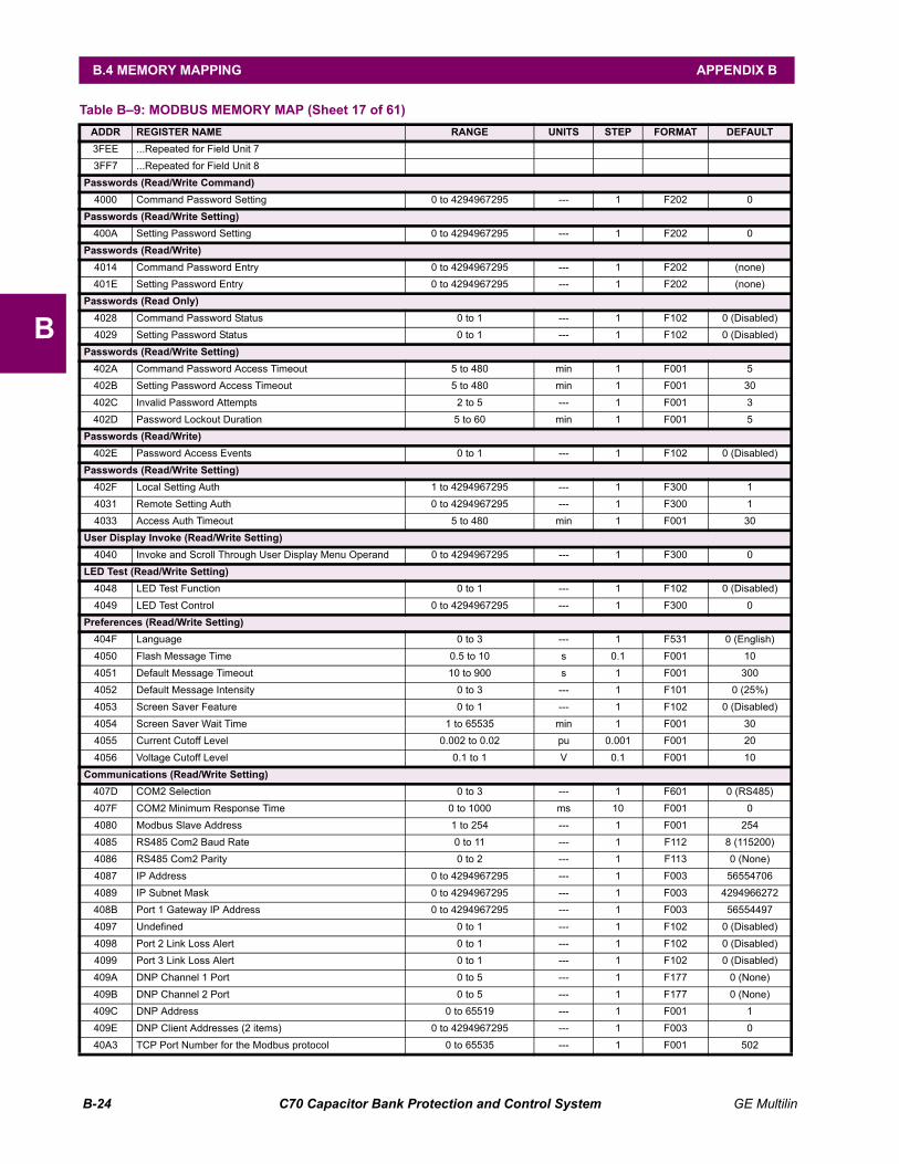
B-24 C70 Capacitor Bank Protection and Control System GE Multilin
B.4 MEMORY MAPPING APPENDIX B
B
3FEE ...Repeated for Field Unit 7
3FF7 ...Repeated for Field Unit 8
Passwords (Read/Write Command)
4000 Command Password Setting 0 to 4294967295 --- 1 F202 0
Passwords (Read/Write Setting)
400A Setting Password Setting 0 to 4294967295 --- 1 F202 0
Passwords (Read/Write)
4014 Command Password Entry 0 to 4294967295 --- 1 F202 (none)
401E Setting Password Entry 0 to 4294967295 --- 1 F202 (none)
Passwords (Read Only)
4028 Command Password Status 0 to 1 --- 1 F102 0 (Disabled)
4029 Setting Password Status 0 to 1 --- 1 F102 0 (Disabled)
Passwords (Read/Write Setting)
402A Command Password Access Timeout 5 to 480 min 1 F001 5
402B Setting Password Access Timeout 5 to 480 min 1 F001 30
402C Invalid Password Attempts 2 to 5 --- 1 F001 3
402D Password Lockout Duration 5 to 60 min 1 F001 5
Passwords (Read/Write)
402E Password Access Events 0 to 1 --- 1 F102 0 (Disabled)
Passwords (Read/Write Setting)
402F Local Setting Auth 1 to 4294967295 --- 1 F300 1
4031 Remote Setting Auth 0 to 4294967295 --- 1 F300 1
4033 Access Auth Timeout 5 to 480 min 1 F001 30
User Display Invoke (Read/Write Setting)
4040 Invoke and Scroll Through User Display Menu Operand 0 to 4294967295 --- 1 F300 0
LED Test (Read/Write Setting)
4048 LED Test Function 0 to 1 --- 1 F102 0 (Disabled)
4049 LED Test Control 0 to 4294967295 --- 1 F300 0
Preferences (Read/Write Setting)
404F Language 0 to 3 --- 1 F531 0 (English)
4050 Flash Message Time 0.5 to 10 s 0.1 F001 10
4051 Default Message Timeout 10 to 900 s 1 F001 300
4052 Default Message Intensity 0 to 3 --- 1 F101 0 (25%)
4053 Screen Saver Feature 0 to 1 --- 1 F102 0 (Disabled)
4054 Screen Saver Wait Time 1 to 65535 min 1 F001 30
4055 Current Cutoff Level 0.002 to 0.02 pu 0.001 F001 20
4056 Voltage Cutoff Level 0.1 to 1 V 0.1 F001 10
Communications (Read/Write Setting)
407D COM2 Selection 0 to 3 --- 1 F601 0 (RS485)
407F COM2 Minimum Response Time 0 to 1000 ms 10 F001 0
4080 Modbus Slave Address 1 to 254 --- 1 F001 254
4085 RS485 Com2 Baud Rate 0 to 11 --- 1 F112 8 (115200)
4086 RS485 Com2 Parity 0 to 2 --- 1 F113 0 (None)
4087 IP Address 0 to 4294967295 --- 1 F003 56554706
4089 IP Subnet Mask 0 to 4294967295 --- 1 F003 4294966272
408B Port 1 Gateway IP Address 0 to 4294967295 --- 1 F003 56554497
4097 Undefined 0 to 1 --- 1 F102 0 (Disabled)
4098 Port 2 Link Loss Alert 0 to 1 --- 1 F102 0 (Disabled)
4099 Port 3 Link Loss Alert 0 to 1 --- 1 F102 0 (Disabled)
409A DNP Channel 1 Port 0 to 5 --- 1 F177 0 (None)
409B DNP Channel 2 Port 0 to 5 --- 1 F177 0 (None)
409C DNP Address 0 to 65519 --- 1 F001 1
409E DNP Client Addresses (2 items) 0 to 4294967295 --- 1 F003 0
40A3 TCP Port Number for the Modbus protocol 0 to 65535 --- 1 F001 502
Table B–9: MODBUS MEMORY MAP (Sheet 17 of 61)
ADDR REGISTER NAME RANGE UNITS STEP FORMAT DEFAULT

GE Multilin C70 Capacitor Bank Protection and Control System B-25
APPENDIX B B.4 MEMORY MAPPING
B
40A4 TCP/UDP Port Number for the DNP Protocol 0 to 65535 --- 1 F001 20000
40A5 TCP Port Number for the HTTP (Web Server) Protocol 0 to 65535 --- 1 F001 80
40A6 Main UDP Port Number for the TFTP Protocol 0 to 65535 --- 1 F001 69
40A7 Data Transfer UDP Port Numbers for the TFTP Protocol (zero means “automatic”) (2 items)
0 to 65535 --- 1 F001 0
40A9 DNP Unsolicited Responses Function 0 to 1 --- 1 F102 0 (Disabled)
40AA DNP Unsolicited Responses Timeout 0 to 60 s 1 F001 5
40AB DNP unsolicited responses maximum retries 1 to 255 --- 1 F001 10
40AC DNP unsolicited responses destination address 0 to 65519 --- 1 F001 1
40AD Ethernet operation mode 0 to 1 --- 1 F192 1 (Half-Duplex)
40AE DNP current scale factor 0 to 8 --- 1 F194 2 (1)
40AF DNP voltage scale factor 0 to 8 --- 1 F194 2 (1)
40B0 DNP power scale factor 0 to 8 --- 1 F194 2 (1)
40B1 DNP energy scale factor 0 to 8 --- 1 F194 2 (1)
40B2 DNP power scale factor 0 to 8 --- 1 F194 2 (1)
40B3 DNP other scale factor 0 to 8 --- 1 F194 2 (1)
40B4 DNP current default deadband 0 to 100000000 --- 1 F003 30000
40B6 DNP voltage default deadband 0 to 100000000 --- 1 F003 30000
40B8 DNP power default deadband 0 to 100000000 --- 1 F003 30000
40BA DNP energy default deadband 0 to 100000000 --- 1 F003 30000
40BC DNP power factor default deadband 0 to 100000000 -- 1 F003 30000
40BE DNP other default deadband 0 to 100000000 --- 1 F003 30000
40C0 DNP IIN time synchronization bit period 1 to 10080 min 1 F001 1440
40C1 DNP message fragment size 30 to 2048 --- 1 F001 240
40C2 DNP client address 3 0 to 4294967295 --- 1 F003 0
40C4 DNP client address 4 0 to 4294967295 --- 1 F003 0
40C6 DNP client address 5 0 to 4294967295 --- 1 F003 0
40C8 DNP number of paired binary output control points 0 to 32 --- 1 F001 0
40C9 DNP TCP connection timeout 10 to 65535 --- 1 F001 120
40CA DNP communications reserved (22 items) 0 to 1 --- 1 F001 0
40E0 TCP port number for the IEC 60870-5-104 protocol 0 to 65535 --- 1 F001 2404
40E1 IEC 60870-5-104 protocol function 0 to 1 --- 1 F102 0 (Disabled)
40E2 IEC 60870-5-104 protocol common address of ASDU 0 to 65535 --- 1 F001 0
40E3 IEC 60870-5-104 protocol cyclic data transmit period 1 to 65535 s 1 F001 60
40E4 IEC 60870-5-104 current default threshold 0 to 100000000 --- 1 F003 30000
40E6 IEC 60870-5-104 voltage default threshold 0 to 100000000 --- 1 F003 30000
40E8 IEC 60870-5-104 power default threshold 0 to 100000000 --- 1 F003 30000
40EA IEC 60870-5-104 energy default threshold 0 to 100000000 --- 1 F003 30000
40EC IEC 60870-5-104 power default threshold 0 to1 --- 0.01 F001 100
40EE IEC 60870-5-104 other default threshold 0 to 100000000 --- 1 F003 30000
40F0 IEC 60870-5-104 client address (5 items) 0 to 4294967295 --- 1 F003 0
4104 IEC 60870-5-104 redundancy port 0 to 1 --- 1 F126 0 (No)
4105 Port 2 IP Address 0 to 4294967295 --- 1 F003 56554706
4107 Port 2 IP Subnet Mask 0 to 4294967295 --- 1 F003 4294966272
4109 Port 2 Gateway IP Address 0 to 4294967295 --- 1 F003 56554497
410B PRT2 Ethernet Operation Mode 0 to 1 --- 1 F192 1 (Full-Duplex)
410C PRT2 Redundancy Enabled 0 to 1 --- 1 F126 0 (No)
410D Port 3 IP Address 0 to 4294967295 --- 1 F003 56554706
410F Port 3 IP Subnet Mask 0 to 4294967295 --- 1 F003 4294966272
4111 Port 3 Gateway IP Address 0 to 4294967295 --- 1 F003 56554497
4113 Port 3 Ethernet Operation Mode 0 to 1 --- 1 F192 1 (Full-Duplex)
4114 PRT1 GOOSE Enabled 0 to 1 --- 1 F102 1 (Enabled)
4115 PRT2 GOOSE Enabled 0 to 1 --- 1 F102 1 (Enabled)
4116 PRT3 GOOSE Enabled 0 to 1 --- 1 F102 1 (Enabled)
Table B–9: MODBUS MEMORY MAP (Sheet 18 of 61)
ADDR REGISTER NAME RANGE UNITS STEP FORMAT DEFAULT

B-26 C70 Capacitor Bank Protection and Control System GE Multilin
B.4 MEMORY MAPPING APPENDIX B
B
4117 IEC Communications Reserved (39 items) 0 to 1 --- 1 F001 0
413E High Enet Traffic Function 0 to 1 --- 1 F102 0 (Disabled)
413F High Enet Traffic Events 0 to 1 --- 1 F102 0 (Disabled)
4140 DNP object 1 default variation 1 to 2 --- 1 F001 2
4141 DNP object 2 default variation 1 to 3 --- 1 F001 2
4142 DNP object 20 default variation 0 to 3 --- 1 F523 0 (1)
4143 DNP object 21 default variation 0 to 3 --- 1 F524 0 (1)
4144 DNP object 22 default variation 0 to 3 --- 1 F523 0 (1)
4145 DNP object 23 default variation 0 to 3 --- 1 F523 0 (1)
4146 DNP object 30 default variation 1 to 5 --- 1 F001 1
4147 DNP object 32 default variation 0 to 5 --- 1 F525 0 (1)
Communications Actuals (Read Only)
4160 Modbus Available TCP/IP Connections 0 to 4 --- 1 F001 4
4161 DNP Available TCP/IP Connections 0 to 2 --- 1 F001 2
4162 IEC Available TCP/IP Connections 0 to 2 --- 1 F001 2
4163 MMS Available TCP/IP Connections 0 to 5 --- 1 F001 5
4164 PMU Available TCP/IP Connections 0 to 4 --- 1 F001 4
Simple Network Time Protocol (Read/Write Setting)
4168 Simple Network Time Protocol (SNTP) function 0 to 1 --- 1 F102 0 (Disabled)
4169 Simple Network Time Protocol (SNTP) server IP address 0 to 4294967295 --- 1 F003 0
416B Simple Network Time Protocol (SNTP) UDP port number 1 to 65535 --- 1 F001 123
Data Logger Commands (Read/Write Command)
4170 Data Logger Clear 0 to 1 --- 1 F126 0 (No)
Data Logger (Read/Write Setting)
4181 Data Logger Channel Settings (16 items) --- --- --- F600 0
4191 Data Logger Mode 0 to 1 --- 1 F260 0 (continuous)
4192 Data Logger Trigger 0 to 4294967295 --- 1 F300 0
4194 Data Logger Rate 15 to 3600000 ms 1 F003 60000
Clock (Read/Write Setting)
419F Synchronizing Source 0 to 3 --- 1 F623 0 (none)
Clock (Read/Write Command)
41A0 Real Time Clock Set Time 0 to 235959 --- 1 F050 0
Clock (Read/Write Setting)
41A2 SR Date Format 0 to 4294967295 --- 1 F051 0
41A4 SR Time Format 0 to 4294967295 --- 1 F052 0
41A6 IRIG-B Signal Type 0 to 2 --- 1 F114 0 (None)
41A7 Clock Events Enable / Disable 0 to 1 --- 1 F102 0 (Disabled)
41A8 Time Zone Offset from UTC –24 to 24 hours 0.5 F002 0
41A9 Daylight Savings Time (DST) Function 0 to 1 --- 1 F102 0 (Disabled)
41AA Daylight Savings Time (DST) Start Month 0 to 11 --- 1 F237 0 (January)
41AB Daylight Savings Time (DST) Start Day 0 to 6 --- 1 F238 0 (Sunday)
41AC Daylight Savings Time (DST) Start Day Instance 0 to 4 --- 1 F239 0 (First)
41AD Daylight Savings Time (DST) Start Hour 0 to 23 --- 1 F001 2
41AE Daylight Savings Time (DST) Stop Month 0 to 11 --- 1 F237 0 (January)
41AF Daylight Savings Time (DST) Stop Day 0 to 6 --- 1 F238 0 (Sunday)
41B0 Daylight Savings Time (DST) Stop Day Instance 0 to 4 --- 1 F239 0 (First)
41B1 Daylight Savings Time (DST) Stop Hour 0 to 23 --- 1 F001 2
Oscillography (Read/Write Setting)
41C0 Oscillography Number of Records 3 to 64 --- 1 F001 15
41C1 Oscillography Trigger Mode 0 to 1 --- 1 F118 0 (Auto. Overwrite)
41C2 Oscillography Trigger Position 0 to 100 % 1 F001 50
41C3 Oscillography Trigger Source 0 to 4294967295 --- 1 F300 0
41C5 Oscillography AC Input Waveforms 0 to 4 --- 1 F183 2 (16 samples/cycle)
Table B–9: MODBUS MEMORY MAP (Sheet 19 of 61)
ADDR REGISTER NAME RANGE UNITS STEP FORMAT DEFAULT

GE Multilin C70 Capacitor Bank Protection and Control System B-27
APPENDIX B B.4 MEMORY MAPPING
B
41D0 Oscillography Analog Channel n (16 items) 0 to 65535 --- 1 F600 0
4200 Oscillography Digital Channel n (63 items) 0 to 4294967295 --- 1 F300 0
Trip and Alarm LEDs (Read/Write Setting)
42B0 Trip LED Input FlexLogic Operand 0 to 4294967295 --- 1 F300 0
42B2 Alarm LED Input FlexLogic Operand 0 to 4294967295 --- 1 F300 0
User Programmable LEDs (Read/Write Setting) (48 modules)
42C0 FlexLogic Operand to Activate LED 0 to 4294967295 --- 1 F300 0
42C2 User LED type (latched or self-resetting) 0 to 1 --- 1 F127 1 (Self-Reset)
42C3 ...Repeated for User-Programmable LED 2
42C6 ...Repeated for User-Programmable LED 3
42C9 ...Repeated for User-Programmable LED 4
42CC ...Repeated for User-Programmable LED 5
42CF ...Repeated for User-Programmable LED 6
42D2 ...Repeated for User-Programmable LED 7
42D5 ...Repeated for User-Programmable LED 8
42D8 ...Repeated for User-Programmable LED 9
42DB ...Repeated for User-Programmable LED 10
42DE ...Repeated for User-Programmable LED 11
42E1 ...Repeated for User-Programmable LED 12
42E4 ...Repeated for User-Programmable LED 13
42E7 ...Repeated for User-Programmable LED 14
42EA ...Repeated for User-Programmable LED 15
42ED ...Repeated for User-Programmable LED 16
42F0 ...Repeated for User-Programmable LED 17
42F3 ...Repeated for User-Programmable LED 18
42F6 ...Repeated for User-Programmable LED 19
42F9 ...Repeated for User-Programmable LED 20
42FC ...Repeated for User-Programmable LED 21
42FF ...Repeated for User-Programmable LED 22
4302 ...Repeated for User-Programmable LED 23
4305 ...Repeated for User-Programmable LED 24
4308 ...Repeated for User-Programmable LED 25
430B ...Repeated for User-Programmable LED 26
430E ...Repeated for User-Programmable LED 27
4311 ...Repeated for User-Programmable LED 28
4314 ...Repeated for User-Programmable LED 29
4317 ...Repeated for User-Programmable LED 30
431A ...Repeated for User-Programmable LED 31
431D ...Repeated for User-Programmable LED 32
4320 ...Repeated for User-Programmable LED 33
4323 ...Repeated for User-Programmable LED 34
4326 ...Repeated for User-Programmable LED 35
4329 ...Repeated for User-Programmable LED 36
432C ...Repeated for User-Programmable LED 37
432F ...Repeated for User-Programmable LED 38
4332 ...Repeated for User-Programmable LED 39
4335 ...Repeated for User-Programmable LED 40
4338 ...Repeated for User-Programmable LED 41
433B ...Repeated for User-Programmable LED 42
433E ...Repeated for User-Programmable LED 43
4341 ...Repeated for User-Programmable LED 44
4344 ...Repeated for User-Programmable LED 45
4347 ...Repeated for User-Programmable LED 46
434A ...Repeated for User-Programmable LED 47
Table B–9: MODBUS MEMORY MAP (Sheet 20 of 61)
ADDR REGISTER NAME RANGE UNITS STEP FORMAT DEFAULT

B-28 C70 Capacitor Bank Protection and Control System GE Multilin
B.4 MEMORY MAPPING APPENDIX B
B
434D ...Repeated for User-Programmable LED 48
Installation (Read/Write Setting)
43E0 Relay Programmed State 0 to 1 --- 1 F133 0 (Not Programmed)
43E1 Relay Name --- --- --- F202 “Relay-1”
User Programmable Self Tests (Read/Write Setting)
4441 User Programmable Detect Ring Break Function 0 to 1 --- 1 F102 1 (Enabled)
4442 User Programmable Direct Device Off Function 0 to 1 --- 1 F102 1 (Enabled)
4443 User Programmable Remote Device Off Function 0 to 1 --- 1 F102 1 (Enabled)
4444 User Programmable First Ethernet Fail Function 0 to 1 --- 1 F102 0 (Disabled)
4445 User Programmable Secondary Ethernet Fail Function 0 to 1 --- 1 F102 0 (Disabled)
4446 User Programmable Battery Fail Function 0 to 1 --- 1 F102 1 (Enabled)
4447 User Programmable SNTP Fail Function 0 to 1 --- 1 F102 1 (Enabled)
4448 User Programmable IRIG-B Fail Function 0 to 1 --- 1 F102 1 (Enabled)
444A Process Bus Failure Operand 0 to 4294967295 --- 1 F300 0
444C PTP Fail Function 0 to 1 --- 1 F102 1 (Enabled)
444D User Programmable Third Ethernet Fail Function 0 to 1 --- 1 F102 0 (Disabled)
444E User Programmable SFP Fail Function 0 to 1 --- 1 F102 0 (Disabled)
CT Settings (Read/Write Setting) (6 modules)
4480 Phase CT 1 Primary 1 to 65000 A 1 F001 1
4481 Phase CT 1 Secondary 0 to 1 --- 1 F123 0 (1 A)
4482 Ground CT 1 Primary 1 to 65000 A 1 F001 1
4483 Ground CT 1 Secondary 0 to 1 --- 1 F123 0 (1 A)
4484 ...Repeated for CT Bank 2
4488 ...Repeated for CT Bank 3
448C ...Repeated for CT Bank 4
4490 ...Repeated for CT Bank 5
4494 ...Repeated for CT Bank 6
VT Settings (Read/Write Setting) (3 modules)
4500 Phase VT 1 Connection 0 to 1 --- 1 F100 0 (Wye)
4501 Phase VT 1 Secondary 25 to 240 V 0.1 F001 664
4502 Phase VT 1 Ratio 1 to 24000 :1 1 F060 1
4504 Auxiliary VT 1 Connection 0 to 6 --- 1 F166 1 (Vag)
4505 Auxiliary VT 1 Secondary 25 to 240 V 0.1 F001 664
4506 Auxiliary VT 1 Ratio 1 to 24000 :1 1 F060 1
4508 ...Repeated for VT Bank 2
4510 ...Repeated for VT Bank 3
4518 ...Repeated for VT Bank 4
4520 ...Repeated for VT Bank 5
4528 ...Repeated for VT Bank 6
Source Settings (Read/Write Setting) (6 modules)
4580 Source 1 Name 0 to 1 --- --- F206 “SRC 1"
4583 Source 1 Phase CT 0 to 63 --- 1 F400 0
4584 Source 1 Ground CT 0 to 63 --- 1 F400 0
4585 Source 1 Phase VT 0 to 63 --- 1 F400 0
4586 Source 1 Auxiliary VT 0 to 63 --- 1 F400 0
4587 ...Repeated for Source 2
458E ...Repeated for Source 3
4595 ...Repeated for Source 4
459C ...Repeated for Source 5
45A3 ...Repeated for Source 6
Power System (Read/Write Setting)
4600 Nominal Frequency 25 to 60 Hz 1 F001 60
4601 Phase Rotation 0 to 1 --- 1 F106 0 (ABC)
Table B–9: MODBUS MEMORY MAP (Sheet 21 of 61)
ADDR REGISTER NAME RANGE UNITS STEP FORMAT DEFAULT
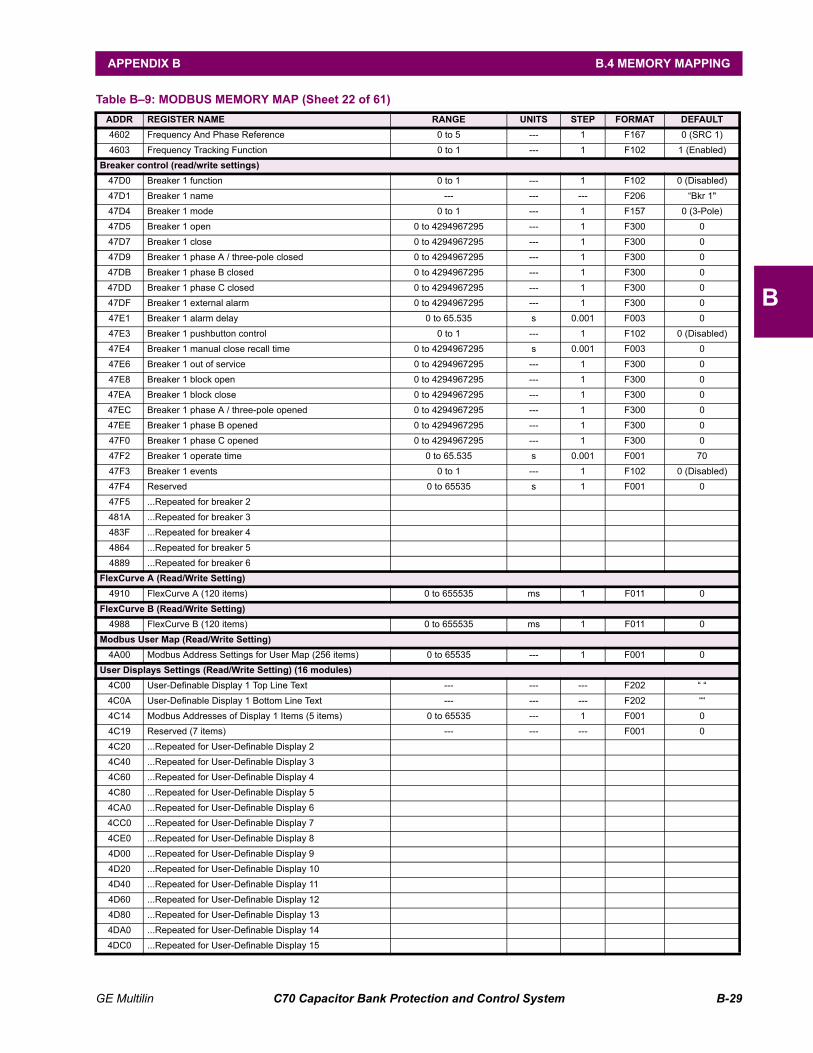
GE Multilin C70 Capacitor Bank Protection and Control System B-29
APPENDIX B B.4 MEMORY MAPPING
B
4602 Frequency And Phase Reference 0 to 5 --- 1 F167 0 (SRC 1)
4603 Frequency Tracking Function 0 to 1 --- 1 F102 1 (Enabled)
Breaker control (read/write settings)
47D0 Breaker 1 function 0 to 1 --- 1 F102 0 (Disabled)
47D1 Breaker 1 name --- --- --- F206 “Bkr 1"
47D4 Breaker 1 mode 0 to 1 --- 1 F157 0 (3-Pole)
47D5 Breaker 1 open 0 to 4294967295 --- 1 F300 0
47D7 Breaker 1 close 0 to 4294967295 --- 1 F300 0
47D9 Breaker 1 phase A / three-pole closed 0 to 4294967295 --- 1 F300 0
47DB Breaker 1 phase B closed 0 to 4294967295 --- 1 F300 0
47DD Breaker 1 phase C closed 0 to 4294967295 --- 1 F300 0
47DF Breaker 1 external alarm 0 to 4294967295 --- 1 F300 0
47E1 Breaker 1 alarm delay 0 to 65.535 s 0.001 F003 0
47E3 Breaker 1 pushbutton control 0 to 1 --- 1 F102 0 (Disabled)
47E4 Breaker 1 manual close recall time 0 to 4294967295 s 0.001 F003 0
47E6 Breaker 1 out of service 0 to 4294967295 --- 1 F300 0
47E8 Breaker 1 block open 0 to 4294967295 --- 1 F300 0
47EA Breaker 1 block close 0 to 4294967295 --- 1 F300 0
47EC Breaker 1 phase A / three-pole opened 0 to 4294967295 --- 1 F300 0
47EE Breaker 1 phase B opened 0 to 4294967295 --- 1 F300 0
47F0 Breaker 1 phase C opened 0 to 4294967295 --- 1 F300 0
47F2 Breaker 1 operate time 0 to 65.535 s 0.001 F001 70
47F3 Breaker 1 events 0 to 1 --- 1 F102 0 (Disabled)
47F4 Reserved 0 to 65535 s 1 F001 0
47F5 ...Repeated for breaker 2
481A ...Repeated for breaker 3
483F ...Repeated for breaker 4
4864 ...Repeated for breaker 5
4889 ...Repeated for breaker 6
FlexCurve A (Read/Write Setting)
4910 FlexCurve A (120 items) 0 to 655535 ms 1 F011 0
FlexCurve B (Read/Write Setting)
4988 FlexCurve B (120 items) 0 to 655535 ms 1 F011 0
Modbus User Map (Read/Write Setting)
4A00 Modbus Address Settings for User Map (256 items) 0 to 65535 --- 1 F001 0
User Displays Settings (Read/Write Setting) (16 modules)
4C00 User-Definable Display 1 Top Line Text --- --- --- F202 “ “
4C0A User-Definable Display 1 Bottom Line Text --- --- --- F202 ““
4C14 Modbus Addresses of Display 1 Items (5 items) 0 to 65535 --- 1 F001 0
4C19 Reserved (7 items) --- --- --- F001 0
4C20 ...Repeated for User-Definable Display 2
4C40 ...Repeated for User-Definable Display 3
4C60 ...Repeated for User-Definable Display 4
4C80 ...Repeated for User-Definable Display 5
4CA0 ...Repeated for User-Definable Display 6
4CC0 ...Repeated for User-Definable Display 7
4CE0 ...Repeated for User-Definable Display 8
4D00 ...Repeated for User-Definable Display 9
4D20 ...Repeated for User-Definable Display 10
4D40 ...Repeated for User-Definable Display 11
4D60 ...Repeated for User-Definable Display 12
4D80 ...Repeated for User-Definable Display 13
4DA0 ...Repeated for User-Definable Display 14
4DC0 ...Repeated for User-Definable Display 15
Table B–9: MODBUS MEMORY MAP (Sheet 22 of 61)
ADDR REGISTER NAME RANGE UNITS STEP FORMAT DEFAULT

B-30 C70 Capacitor Bank Protection and Control System GE Multilin
B.4 MEMORY MAPPING APPENDIX B
B
4DE0 ...Repeated for User-Definable Display 16
Field Unit Raw Data Actuals (Read Only) (8 modules)
4E00 Raw Field Data AC1 Mag 0 to 0.001 A 0.001 F003 0
4E02 Raw Field Data AC1 Angle 0 to 0.1 degree 0.1 F002 0
4E03 Raw Field Data AC2 Mag 0 to 0.001 A 0.001 F003 0
4E05 Raw Field Data AC2 Angle 0 to 0.1 degree 0.1 F002 0
4E06 Raw Field Data AC3 Mag 0 to 0.001 A 0.001 F003 0
4E08 Raw Field Data AC3 Angle 0 to 0.01 degree 0.1 F002 0
4E09 Raw Field Data AC4 Mag 0 to 0.001 A 0.001 F003 0
4E0B Raw Field Data AC4 Angle 0 to 0.01 degree 0.1 F002 0
4E0C Raw Field Data AC5 Mag 0 to 0.001 A/V 0.001 F003 0
4E0E Raw Field Data AC5 Angle 0 to 0.01 degree 0.1 F002 0
4E0F Raw Field Data AC6 Mag 0 to 0.001 A/V 0.001 F003 0
4E11 Raw Field Data AC6 Angle 0 to 0.01 degree 0.1 F002 0
4E12 Raw Field Data AC7 Mag 0 to 0.001 A/V 0.001 F003 0
4E14 Raw Field Data AC7 Angle 0 to 0.01 degree 0.1 F002 0
4E15 Raw Field Data AC8 Mag 0 to 0.001 A/V 0.001 F003 0
4E17 Raw Field Data AC8 Angle 0 to 0.01 degree 0.1 F002 0
4E18 Raw Field Data DC1 0 to 0.001 V 0.001 F002 0
4E19 Raw Field Data DC2 0 to 0.001 V 0.001 F002 0
4E1A Raw Field Data DC3 0 to 0.001 V 0.001 F002 0
4E1B Raw Field Data FCI States (2 items) 0 to 1 --- 1 F500 0
4E1D Raw Field Data SI States 0 to 1 --- 1 F500 0
4E1E Raw Field Data SI Test States 0 to 1 --- 1 F500 0
4E1F Raw Field Data Brick ADC Temperature 0 to 1 degree 1 F002 0
4E20 Raw Field Data Brick Transceiver Temperature 0 to 1 degree 1 F002 0
4E21 Raw Field Data Brick Transceiver Voltage 0 to 0.01 V 0.01 F001 0
4E22 Raw Field Data Brick Transceiver Current 0 to 1 mA 1 F001 0
4E23 Raw Field Data Brick Tx Power 0 to 0.01 dBm 0.1 F002 0
4E24 Raw Field Data Brick Rx Power 0 to 0.1 dBm 0.1 F002 0
4E25 Raw Field Data Brick Diagnostics (2 items) 0 to 65535 --- 1 F500 0
4E27 Raw Field Data Local Transceiver Temperature 0 to 1 degree 1 F002 0
4E28 Raw Field Data Local Transceiver Voltage 0 to 0.01 V 0.01 F001 0
4E29 Raw Field Data Local Transceiver Current 0 to 1 mA 1 F001 0
4E2A Raw Field Data Local Tx Power 0 to 0.1 dBm 0.1 F002 0
4E2B Raw Field Data Local Rx Power 0 to 0.1 dBm 0.1 F002 0
4E2C Repeated for module number 2
4E58 Repeated for module number 3
4E84 Repeated for module number 4
4E80 Repeated for module number 5
4EDC Repeated for module number 6
4F08 Repeated for module number 7
4F34 Repeated for module number 8
Flexlogic (Read/Write Setting)
5000 FlexLogic Entry (512 items) 0 to 4294967295 --- 1 F300 2097152
RTD Inputs (Read/Write Setting) (48 modules)
5400 RTD Input 1 Function 0 to 1 --- 1 F102 0 (Disabled)
5401 RTD Input 1 ID --- --- --- F205 “RTD Ip 1“
5407 RTD Input 1 Type 0 to 3 --- 1 F174 0 (100 ohm Platinum)
5414 ...Repeated for RTD Input 2
5428 ...Repeated for RTD Input 3
543C ...Repeated for RTD Input 4
5450 ...Repeated for RTD Input 5
Table B–9: MODBUS MEMORY MAP (Sheet 23 of 61)
ADDR REGISTER NAME RANGE UNITS STEP FORMAT DEFAULT
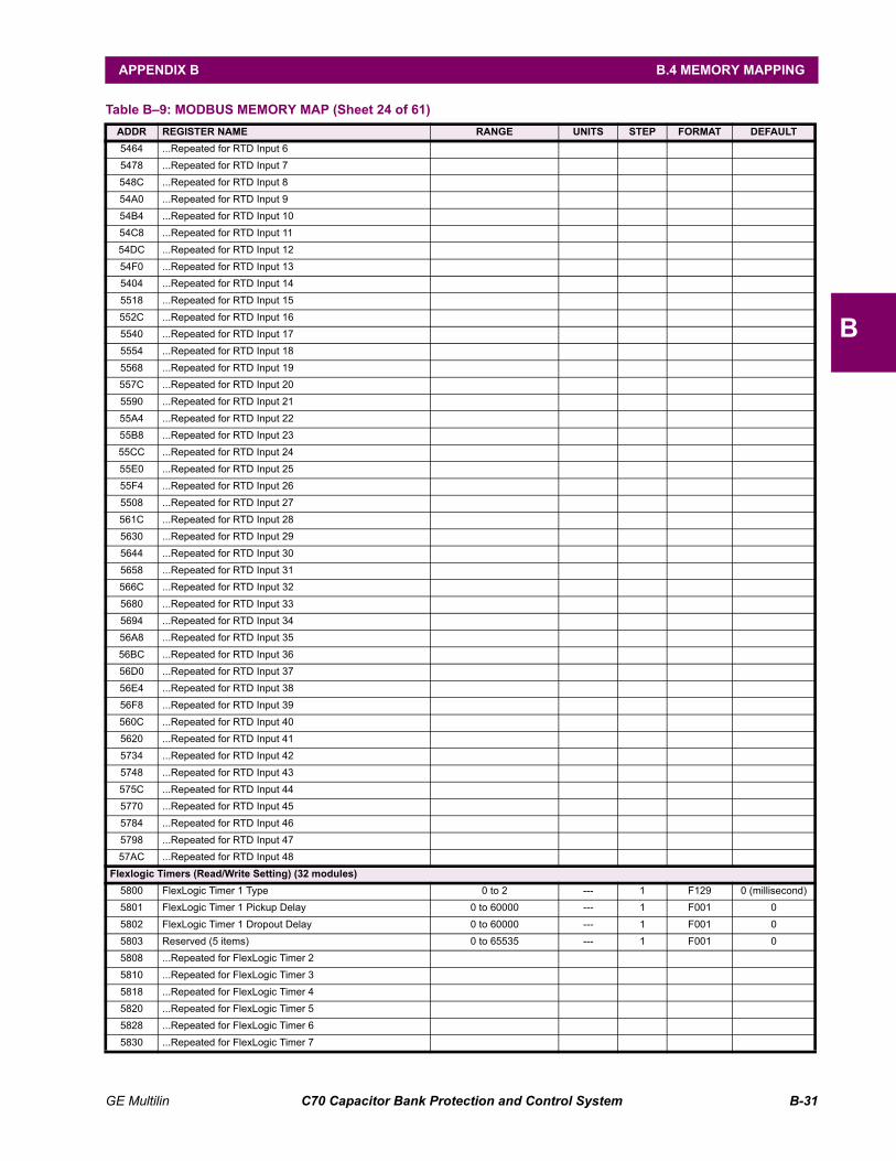
GE Multilin C70 Capacitor Bank Protection and Control System B-31
APPENDIX B B.4 MEMORY MAPPING
B
5464 ...Repeated for RTD Input 6
5478 ...Repeated for RTD Input 7
548C ...Repeated for RTD Input 8
54A0 ...Repeated for RTD Input 9
54B4 ...Repeated for RTD Input 10
54C8 ...Repeated for RTD Input 11
54DC ...Repeated for RTD Input 12
54F0 ...Repeated for RTD Input 13
5404 ...Repeated for RTD Input 14
5518 ...Repeated for RTD Input 15
552C ...Repeated for RTD Input 16
5540 ...Repeated for RTD Input 17
5554 ...Repeated for RTD Input 18
5568 ...Repeated for RTD Input 19
557C ...Repeated for RTD Input 20
5590 ...Repeated for RTD Input 21
55A4 ...Repeated for RTD Input 22
55B8 ...Repeated for RTD Input 23
55CC ...Repeated for RTD Input 24
55E0 ...Repeated for RTD Input 25
55F4 ...Repeated for RTD Input 26
5508 ...Repeated for RTD Input 27
561C ...Repeated for RTD Input 28
5630 ...Repeated for RTD Input 29
5644 ...Repeated for RTD Input 30
5658 ...Repeated for RTD Input 31
566C ...Repeated for RTD Input 32
5680 ...Repeated for RTD Input 33
5694 ...Repeated for RTD Input 34
56A8 ...Repeated for RTD Input 35
56BC ...Repeated for RTD Input 36
56D0 ...Repeated for RTD Input 37
56E4 ...Repeated for RTD Input 38
56F8 ...Repeated for RTD Input 39
560C ...Repeated for RTD Input 40
5620 ...Repeated for RTD Input 41
5734 ...Repeated for RTD Input 42
5748 ...Repeated for RTD Input 43
575C ...Repeated for RTD Input 44
5770 ...Repeated for RTD Input 45
5784 ...Repeated for RTD Input 46
5798 ...Repeated for RTD Input 47
57AC ...Repeated for RTD Input 48
Flexlogic Timers (Read/Write Setting) (32 modules)
5800 FlexLogic Timer 1 Type 0 to 2 --- 1 F129 0 (millisecond)
5801 FlexLogic Timer 1 Pickup Delay 0 to 60000 --- 1 F001 0
5802 FlexLogic Timer 1 Dropout Delay 0 to 60000 --- 1 F001 0
5803 Reserved (5 items) 0 to 65535 --- 1 F001 0
5808 ...Repeated for FlexLogic Timer 2
5810 ...Repeated for FlexLogic Timer 3
5818 ...Repeated for FlexLogic Timer 4
5820 ...Repeated for FlexLogic Timer 5
5828 ...Repeated for FlexLogic Timer 6
5830 ...Repeated for FlexLogic Timer 7
Table B–9: MODBUS MEMORY MAP (Sheet 24 of 61)
ADDR REGISTER NAME RANGE UNITS STEP FORMAT DEFAULT

B-32 C70 Capacitor Bank Protection and Control System GE Multilin
B.4 MEMORY MAPPING APPENDIX B
B
5838 ...Repeated for FlexLogic Timer 8
5840 ...Repeated for FlexLogic Timer 9
5848 ...Repeated for FlexLogic Timer 10
5850 ...Repeated for FlexLogic Timer 11
5858 ...Repeated for FlexLogic Timer 12
5860 ...Repeated for FlexLogic Timer 13
5868 ...Repeated for FlexLogic Timer 14
5870 ...Repeated for FlexLogic Timer 15
5878 ...Repeated for FlexLogic Timer 16
5880 ...Repeated for FlexLogic Timer 17
5888 ...Repeated for FlexLogic Timer 18
5890 ...Repeated for FlexLogic Timer 19
5898 ...Repeated for FlexLogic Timer 20
58A0 ...Repeated for FlexLogic Timer 21
58A8 ...Repeated for FlexLogic Timer 22
58B0 ...Repeated for FlexLogic Timer 23
58B8 ...Repeated for FlexLogic Timer 24
58C0 ...Repeated for FlexLogic Timer 25
58C8 ...Repeated for FlexLogic Timer 26
58D0 ...Repeated for FlexLogic Timer 27
58D8 ...Repeated for FlexLogic Timer 28
58E0 ...Repeated for FlexLogic Timer 29
58E8 ...Repeated for FlexLogic Timer 30
58F0 ...Repeated for FlexLogic Timer 31
58F8 ...Repeated for FlexLogic Timer 32
Phase Time Overcurrent (Read/Write Grouped Setting) (6 modules)
5900 Phase Time Overcurrent 1 Function 0 to 1 --- 1 F102 0 (Disabled)
5901 Phase Time Overcurrent 1 Signal Source 0 to 5 --- 1 F167 0 (SRC 1)
5902 Phase Time Overcurrent 1 Input 0 to 1 --- 1 F122 0 (Phasor)
5903 Phase Time Overcurrent 1 Pickup 0 to 30 pu 0.001 F001 1000
5904 Phase Time Overcurrent 1 Curve 0 to 16 --- 1 F103 0 (IEEE Mod Inv)
5905 Phase Time Overcurrent 1 Multiplier 0 to 600 --- 0.01 F001 100
5906 Phase Time Overcurrent 1 Reset 0 to 1 --- 1 F104 0 (Instantaneous)
5907 Phase Time Overcurrent 1 Voltage Restraint 0 to 1 --- 1 F102 0 (Disabled)
5908 Phase TOC 1 Block For Each Phase (3 items) 0 to 4294967295 --- 1 F300 0
590F Phase Time Overcurrent 1 Target 0 to 2 --- 1 F109 0 (Self-reset)
5910 Phase Time Overcurrent 1 Events 0 to 1 --- 1 F102 0 (Disabled)
5911 Reserved (3 items) 0 to 1 --- 1 F001 0
5914 ...Repeated for Phase Time Overcurrent 2
5928 ...Repeated for Phase Time Overcurrent 3
593C ...Repeated for Phase Time Overcurrent 4
5950 ...Repeated for Phase Time Overcurrent 5
5964 ...Repeated for Phase Time Overcurrent 6
Phase Instantaneous Overcurrent (Read/Write Grouped Setting) (12 modules)
5A00 Phase Instantaneous Overcurrent 1 Function 0 to 1 --- 1 F102 0 (Disabled)
5A01 Phase Instantaneous Overcurrent 1 Signal Source 0 to 5 --- 1 F167 0 (SRC 1)
5A02 Phase Instantaneous Overcurrent 1 Pickup 0 to 30 pu 0.001 F001 1000
5A03 Phase Instantaneous Overcurrent 1 Delay 0 to 600 s 0.01 F001 0
5A04 Phase Instantaneous Overcurrent 1 Reset Delay 0 to 600 s 0.01 F001 0
5A05 Phase IOC1 Block For Each Phase (3 items) 0 to 4294967295 --- 1 F300 0
5A0B Phase Instantaneous Overcurrent 1 Target 0 to 2 --- 1 F109 0 (Self-reset)
5A0C Phase Instantaneous Overcurrent 1 Events 0 to 1 --- 1 F102 0 (Disabled)
5A0D Reserved (6 items) 0 to 1 --- 1 F001 0
5A13 ...Repeated for Phase Instantaneous Overcurrent 2
Table B–9: MODBUS MEMORY MAP (Sheet 25 of 61)
ADDR REGISTER NAME RANGE UNITS STEP FORMAT DEFAULT

GE Multilin C70 Capacitor Bank Protection and Control System B-33
APPENDIX B B.4 MEMORY MAPPING
B
5A26 ...Repeated for Phase Instantaneous Overcurrent 3
5A39 ...Repeated for Phase Instantaneous Overcurrent 4
5A4C ...Repeated for Phase Instantaneous Overcurrent 5
5A5F ...Repeated for Phase Instantaneous Overcurrent 6
5A72 ...Repeated for Phase Instantaneous Overcurrent 7
5A85 ...Repeated for Phase Instantaneous Overcurrent 8
5A98 ...Repeated for Phase Instantaneous Overcurrent 9
5AAB ...Repeated for Phase Instantaneous Overcurrent 10
5ABE ...Repeated for Phase Instantaneous Overcurrent 11
5AD1 ...Repeated for Phase Instantaneous Overcurrent 12
Neutral Time Overcurrent (Read/Write Grouped Setting) (6 modules)
5B00 Neutral Time Overcurrent 1 Function 0 to 1 --- 1 F102 0 (Disabled)
5B01 Neutral Time Overcurrent 1 Signal Source 0 to 5 --- 1 F167 0 (SRC 1)
5B02 Neutral Time Overcurrent 1 Input 0 to 1 --- 1 F122 0 (Phasor)
5B03 Neutral Time Overcurrent 1 Pickup 0 to 30 pu 0.001 F001 1000
5B04 Neutral Time Overcurrent 1 Curve 0 to 16 --- 1 F103 0 (IEEE Mod Inv)
5B05 Neutral Time Overcurrent 1 Multiplier 0 to 600 --- 0.01 F001 100
5B06 Neutral Time Overcurrent 1 Reset 0 to 1 --- 1 F104 0 (Instantaneous)
5B07 Neutral Time Overcurrent 1 Block 0 to 4294967295 --- 1 F300 0
5B09 Neutral Time Overcurrent 1 Target 0 to 2 --- 1 F109 0 (Self-reset)
5B0A Neutral Time Overcurrent 1 Events 0 to 1 --- 1 F102 0 (Disabled)
5B0B Reserved (6 items) 0 to 1 --- 1 F001 0
5B11 ...Repeated for Neutral Time Overcurrent 2
5B22 ...Repeated for Neutral Time Overcurrent 3
5B33 ...Repeated for Neutral Time Overcurrent 4
5B44 ...Repeated for Neutral Time Overcurrent 5
5B55 ...Repeated for Neutral Time Overcurrent 6
Neutral Instantaneous Overcurrent (Read/Write Grouped Setting) (12 modules)
5C00 Neutral Instantaneous Overcurrent 1 Function 0 to 1 --- 1 F102 0 (Disabled)
5C01 Neutral Instantaneous Overcurrent 1 Signal Source 0 to 5 --- 1 F167 0 (SRC 1)
5C02 Neutral Instantaneous Overcurrent 1 Pickup 0 to 30 pu 0.001 F001 1000
5C03 Neutral Instantaneous Overcurrent 1 Delay 0 to 600 s 0.01 F001 0
5C04 Neutral Instantaneous Overcurrent 1 Reset Delay 0 to 600 s 0.01 F001 0
5C05 Neutral Instantaneous Overcurrent 1 Block 0 to 4294967295 --- 1 F300 0
5C07 Neutral Instantaneous Overcurrent 1 Target 0 to 2 --- 1 F109 0 (Self-reset)
5C08 Neutral Instantaneous Overcurrent 1 Events 0 to 1 --- 1 F102 0 (Disabled)
5C09 Reserved (8 items) 0 to 1 --- 1 F001 0
5C11 ...Repeated for Neutral Instantaneous Overcurrent 2
5C22 ...Repeated for Neutral Instantaneous Overcurrent 3
5C33 ...Repeated for Neutral Instantaneous Overcurrent 4
5C44 ...Repeated for Neutral Instantaneous Overcurrent 5
5C55 ...Repeated for Neutral Instantaneous Overcurrent 6
5C66 ...Repeated for Neutral Instantaneous Overcurrent 7
5C77 ...Repeated for Neutral Instantaneous Overcurrent 8
5C88 ...Repeated for Neutral Instantaneous Overcurrent 9
5C99 ...Repeated for Neutral Instantaneous Overcurrent 10
5CAA ...Repeated for Neutral Instantaneous Overcurrent 11
5CBB ...Repeated for Neutral Instantaneous Overcurrent 12
Ground Time Overcurrent (Read/Write Grouped Setting) (6 modules)
5D00 Ground Time Overcurrent 1 Function 0 to 1 --- 1 F102 0 (Disabled)
5D01 Ground Time Overcurrent 1 Signal Source 0 to 5 --- 1 F167 0 (SRC 1)
5D02 Ground Time Overcurrent 1 Input 0 to 1 --- 1 F122 0 (Phasor)
5D03 Ground Time Overcurrent 1 Pickup 0 to 30 pu 0.001 F001 1000
5D04 Ground Time Overcurrent 1 Curve 0 to 16 --- 1 F103 0 (IEEE Mod Inv)
Table B–9: MODBUS MEMORY MAP (Sheet 26 of 61)
ADDR REGISTER NAME RANGE UNITS STEP FORMAT DEFAULT
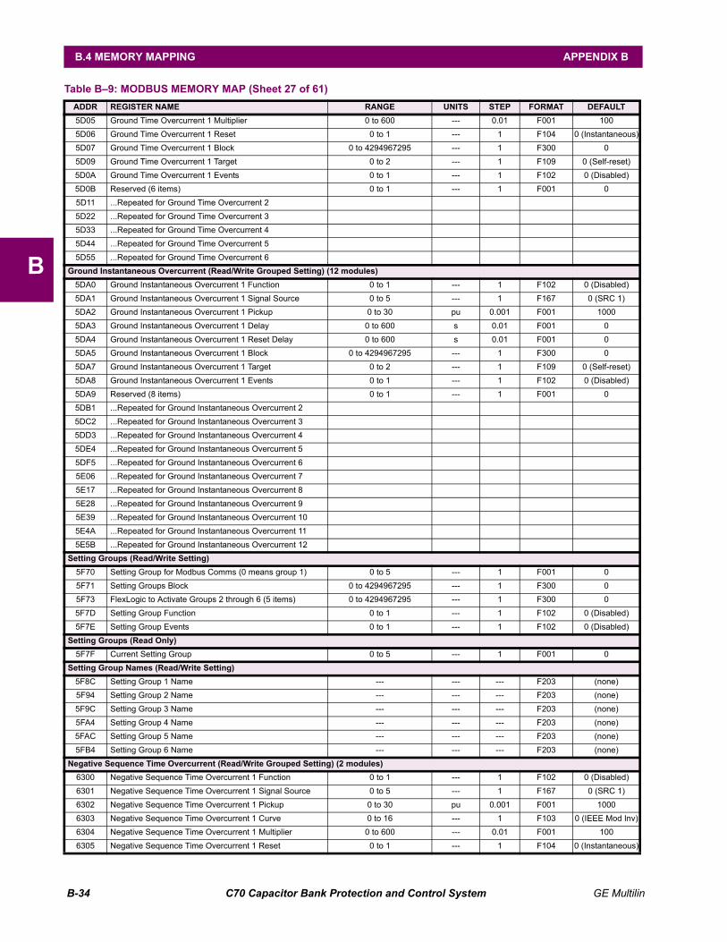
B-34 C70 Capacitor Bank Protection and Control System GE Multilin
B.4 MEMORY MAPPING APPENDIX B
B
5D05 Ground Time Overcurrent 1 Multiplier 0 to 600 --- 0.01 F001 100
5D06 Ground Time Overcurrent 1 Reset 0 to 1 --- 1 F104 0 (Instantaneous)
5D07 Ground Time Overcurrent 1 Block 0 to 4294967295 --- 1 F300 0
5D09 Ground Time Overcurrent 1 Target 0 to 2 --- 1 F109 0 (Self-reset)
5D0A Ground Time Overcurrent 1 Events 0 to 1 --- 1 F102 0 (Disabled)
5D0B Reserved (6 items) 0 to 1 --- 1 F001 0
5D11 ...Repeated for Ground Time Overcurrent 2
5D22 ...Repeated for Ground Time Overcurrent 3
5D33 ...Repeated for Ground Time Overcurrent 4
5D44 ...Repeated for Ground Time Overcurrent 5
5D55 ...Repeated for Ground Time Overcurrent 6
Ground Instantaneous Overcurrent (Read/Write Grouped Setting) (12 modules)
5DA0 Ground Instantaneous Overcurrent 1 Function 0 to 1 --- 1 F102 0 (Disabled)
5DA1 Ground Instantaneous Overcurrent 1 Signal Source 0 to 5 --- 1 F167 0 (SRC 1)
5DA2 Ground Instantaneous Overcurrent 1 Pickup 0 to 30 pu 0.001 F001 1000
5DA3 Ground Instantaneous Overcurrent 1 Delay 0 to 600 s 0.01 F001 0
5DA4 Ground Instantaneous Overcurrent 1 Reset Delay 0 to 600 s 0.01 F001 0
5DA5 Ground Instantaneous Overcurrent 1 Block 0 to 4294967295 --- 1 F300 0
5DA7 Ground Instantaneous Overcurrent 1 Target 0 to 2 --- 1 F109 0 (Self-reset)
5DA8 Ground Instantaneous Overcurrent 1 Events 0 to 1 --- 1 F102 0 (Disabled)
5DA9 Reserved (8 items) 0 to 1 --- 1 F001 0
5DB1 ...Repeated for Ground Instantaneous Overcurrent 2
5DC2 ...Repeated for Ground Instantaneous Overcurrent 3
5DD3 ...Repeated for Ground Instantaneous Overcurrent 4
5DE4 ...Repeated for Ground Instantaneous Overcurrent 5
5DF5 ...Repeated for Ground Instantaneous Overcurrent 6
5E06 ...Repeated for Ground Instantaneous Overcurrent 7
5E17 ...Repeated for Ground Instantaneous Overcurrent 8
5E28 ...Repeated for Ground Instantaneous Overcurrent 9
5E39 ...Repeated for Ground Instantaneous Overcurrent 10
5E4A ...Repeated for Ground Instantaneous Overcurrent 11
5E5B ...Repeated for Ground Instantaneous Overcurrent 12
Setting Groups (Read/Write Setting)
5F70 Setting Group for Modbus Comms (0 means group 1) 0 to 5 --- 1 F001 0
5F71 Setting Groups Block 0 to 4294967295 --- 1 F300 0
5F73 FlexLogic to Activate Groups 2 through 6 (5 items) 0 to 4294967295 --- 1 F300 0
5F7D Setting Group Function 0 to 1 --- 1 F102 0 (Disabled)
5F7E Setting Group Events 0 to 1 --- 1 F102 0 (Disabled)
Setting Groups (Read Only)
5F7F Current Setting Group 0 to 5 --- 1 F001 0
Setting Group Names (Read/Write Setting)
5F8C Setting Group 1 Name --- --- --- F203 (none)
5F94 Setting Group 2 Name --- --- --- F203 (none)
5F9C Setting Group 3 Name --- --- --- F203 (none)
5FA4 Setting Group 4 Name --- --- --- F203 (none)
5FAC Setting Group 5 Name --- --- --- F203 (none)
5FB4 Setting Group 6 Name --- --- --- F203 (none)
Negative Sequence Time Overcurrent (Read/Write Grouped Setting) (2 modules)
6300 Negative Sequence Time Overcurrent 1 Function 0 to 1 --- 1 F102 0 (Disabled)
6301 Negative Sequence Time Overcurrent 1 Signal Source 0 to 5 --- 1 F167 0 (SRC 1)
6302 Negative Sequence Time Overcurrent 1 Pickup 0 to 30 pu 0.001 F001 1000
6303 Negative Sequence Time Overcurrent 1 Curve 0 to 16 --- 1 F103 0 (IEEE Mod Inv)
6304 Negative Sequence Time Overcurrent 1 Multiplier 0 to 600 --- 0.01 F001 100
6305 Negative Sequence Time Overcurrent 1 Reset 0 to 1 --- 1 F104 0 (Instantaneous)
Table B–9: MODBUS MEMORY MAP (Sheet 27 of 61)
ADDR REGISTER NAME RANGE UNITS STEP FORMAT DEFAULT

GE Multilin C70 Capacitor Bank Protection and Control System B-35
APPENDIX B B.4 MEMORY MAPPING
B
6306 Negative Sequence Time Overcurrent 1 Block 0 to 4294967295 --- 1 F300 0
6308 Negative Sequence Time Overcurrent 1 Target 0 to 2 --- 1 F109 0 (Self-reset)
6309 Negative Sequence Time Overcurrent 1 Events 0 to 1 --- 1 F102 0 (Disabled)
630A Reserved (7 items) 0 to 1 --- 1 F001 0
6311 ...Repeated for Negative Sequence Time Overcurrent 2
Capacitor bank overvoltage settings (read/write, grouped, 3 modules)
6330 Bank phase overvoltage 1 function 0 to 1 --- 1 F102 0 (Disabled)
6331 Bank phase overvoltage 1 bus source 0 to 5 --- 1 F167 0 (SRC 1)
6332 Bank phase overvoltage 1 neutral source 0 to 5 --- 1 F167 0 (SRC 1)
6333 Bank phase overvoltage 1 bank ground 0 to 2 --- 1 F093 0 (Grounded)
6334 Bank phase overvoltage 1 curve 0 to 3 --- 1 F094 0 (FlexCurve A)
6335 Bank phase overvoltage 1 curve time multiplier 1 to 10 --- 0.01 F001 100
6336 Bank phase overvoltage 1 stage 1A pickup 0.8 to 2 pu 0.001 F001 1050
6337 Bank phase overvoltage 1 stage 2A pickup 0.8 to 2 pu 0.001 F001 1100
6338 Bank phase overvoltage 1 stage 3A pickup 0.8 to 2 pu 0.001 F001 1200
6339 Bank phase overvoltage 1 stage 4A pickup 0.8 to 2 pu 0.001 F001 1050
633A Bank phase overvoltage 1 stage 1B pickup 0.8 to 2 pu 0.001 F001 1050
633B Bank phase overvoltage 1 stage 2B pickup 0.8 to 2 pu 0.001 F001 1100
633C Bank phase overvoltage 1 stage 3B pickup 0.8 to 2 pu 0.001 F001 1200
633D Bank phase overvoltage 1 stage 4B pickup 0.8 to 2 pu 0.001 F001 1050
633E Bank phase overvoltage 1 stage 1C pickup 0.8 to 2 pu 0.001 F001 1050
633F Bank phase overvoltage 1 stage 2C pickup 0.8 to 2 pu 0.001 F001 1100
6340 Bank phase overvoltage 1 stage 3C pickup 0.8 to 2 pu 0.001 F001 1200
6341 Bank phase overvoltage 1 stage 4C pickup 0.8 to 2 pu 0.001 F001 1050
6342 Bank phase overvoltage 1 stage 1 pickup delay 0 to 600 s 0.01 F001 6000
6343 Bank phase overvoltage 1 stage 2 pickup delay 0 to 600 s 0.01 F001 1000
6344 Bank phase overvoltage 1 stage 3 pickup delay 0 to 600 s 0.01 F001 200
6345 Bank phase overvoltage 1 dropout delay 0 to 600 s 0.01 F001 25
6346 Bank phase overvoltage 1 block 0 to 4294967295 --- 1 F300 0
6348 Bank phase overvoltage 1 target 0 to 2 --- 1 F109 0 (Self-reset)
6349 Bank phase overvoltage 1 events 0 to 1 --- 1 F102 0 (Disabled)
634A ...Repeated for bank phase overvoltage 2
6364 ...Repeated for bank phase overvoltage 3
Capacitor bank overvoltage actual values (read only, 3 modules)
6390 Bank overvoltage 1 phase A operate voltage 0 to 65.535 pu 0.001 F001 0
6391 Bank overvoltage 1 phase B operate voltage 0 to 65.535 pu 0.001 F001 0
6392 Bank overvoltage 1 phase C operate voltage 0 to 65.535 pu 0.001 F001 0
6393 ...Repeated for bank phase overvoltage 2
6396 ...Repeated for bank phase overvoltage 3
Negative Sequence Instantaneous Overcurrent (Read/Write Grouped Setting) (2 modules)
63C0 Negative Sequence Instantaneous OC 1 Function 0 to 1 --- 1 F102 0 (Disabled)
63C1 Negative Sequence Instantaneous OC 1 Signal Source 0 to 5 --- 1 F167 0 (SRC 1)
63C2 Negative Sequence Instantaneous Overcurrent 1 Pickup 0 to 30 pu 0.001 F001 1000
63C3 Negative Sequence Instantaneous Overcurrent 1 Delay 0 to 600 s 0.01 F001 0
63C4 Negative Sequence Instantaneous OC 1 Reset Delay 0 to 600 s 0.01 F001 0
63C5 Negative Sequence Instantaneous Overcurrent 1 Block 0 to 4294967295 --- 1 F300 0
63C7 Negative Sequence Instantaneous Overcurrent 1 Target 0 to 2 --- 1 F109 0 (Self-reset)
63C8 Negative Sequence Instantaneous Overcurrent 1 Events 0 to 1 --- 1 F102 0 (Disabled)
63C9 Reserved (8 items) 0 to 1 --- 1 F001 0
63D1 ...Repeated for Negative Sequence Instantaneous OC 2
Negative Sequence Overvoltage (Read/Write Grouped Setting)
6440 Negative Sequence Overvoltage Function 0 to 1 --- 1 F102 0 (Disabled)
6441 Negative Sequence Overvoltage Source 0 to 5 --- 1 F167 0 (SRC 1)
64A42 Negative Sequence Overvoltage Pickup 0 to 1.25 pu 0.001 F001 300
Table B–9: MODBUS MEMORY MAP (Sheet 28 of 61)
ADDR REGISTER NAME RANGE UNITS STEP FORMAT DEFAULT

B-36 C70 Capacitor Bank Protection and Control System GE Multilin
B.4 MEMORY MAPPING APPENDIX B
B
6443 Negative Sequence Overvoltage Pickup Delay 0 to 600 s 0.01 F001 50
6444 Negative Sequence Overvoltage Reset Delay 0 to 600 s 0.01 F001 50
6445 Negative Sequence Overvoltage Block 0 to 4294967295 --- 1 F300 0
6447 Negative Sequence Overvoltage Target 0 to 2 --- 1 F109 0 (Self-reset)
6448 Negative Sequence Overvoltage Events 0 to 1 --- 1 F102 0 (Disabled)
6449 ...Repeated for module number 2
6452 ...Repeated for module number 3
Time of day timer settings (read/write, grouped, 5 modules)
6570 Time of day timer 1 function 0 to 1 --- 1 F102 0 (Disabled)
6571 Time of day timer 1 start time 0 to 2359 --- 1 F050 0
6573 Time of day timer 1 stop time 0 to 2359 --- 1 F001 2359
6575 Time of day timer 1 targets 0 to 2 --- 1 F109 0 (Self-reset)
6576 Time of day timer 1 events 0 to 1 --- 1 F102 0 (Disabled)
6577 ...Repeated for time of day timer 2
657E ...Repeated for time of day timer 3
6585 ...Repeated for time of day timer 4
658C ...Repeated for time of day timer 5
Phase Undervoltage (Read/Write Grouped Setting) (2 modules)
7000 Phase Undervoltage 1 Function 0 to 1 --- 1 F102 0 (Disabled)
7001 Phase Undervoltage 1 Signal Source 0 to 5 --- 1 F167 0 (SRC 1)
7002 Phase Undervoltage 1 Pickup 0 to 3 pu 0.001 F001 1000
7003 Phase Undervoltage 1 Curve 0 to 1 --- 1 F111 0 (Definite Time)
7004 Phase Undervoltage 1 Delay 0 to 600 s 0.01 F001 100
7005 Phase Undervoltage 1 Minimum Voltage 0 to 3 pu 0.001 F001 100
7006 Phase Undervoltage 1 Block 0 to 4294967295 --- 1 F300 0
7008 Phase Undervoltage 1 Target 0 to 2 --- 1 F109 0 (Self-reset)
7009 Phase Undervoltage 1 Events 0 to 1 --- 1 F102 0 (Disabled)
700A Phase Undervoltage 1 Measurement Mode 0 to 1 --- 1 F186 0 (Phase to Ground)
700A Reserved (6 items) 0 to 1 --- 1 F001 0
7013 ...Repeated for Phase Undervoltage 2
7015 ...Repeated for Phase Undervoltage 2
7017 ...Repeated for Phase Undervoltage 2
701B ...Repeated for Phase Undervoltage 2
701C ...Repeated for Phase Undervoltage 2
7022 ...Repeated for Phase Undervoltage 3
7025 ...Repeated for Phase Undervoltage 3
7027 ...Repeated for Phase Undervoltage 3
7028 ...Repeated for Phase Undervoltage 3
702A ...Repeated for Phase Undervoltage 3
Phase Overvoltage (Read/Write Grouped Setting)
7040 Phase Overvoltage 1 Function 0 to 1 --- 1 F102 0 (Disabled)
7041 Phase Overvoltage 1 Source 0 to 5 --- 1 F167 0 (SRC 1)
7042 Phase Overvoltage 1 Pickup 0 to 3 pu 0.001 F001 1000
7043 Phase Overvoltage 1 Delay 0 to 600 s 0.01 F001 100
7044 Phase Overvoltage 1 Reset Delay 0 to 600 s 0.01 F001 100
7045 Phase Overvoltage 1 Block 0 to 4294967295 --- 1 F300 0
7047 Phase Overvoltage 1 Target 0 to 2 --- 1 F109 0 (Self-reset)
7048 Phase Overvoltage 1 Events 0 to 1 --- 1 F102 0 (Disabled)
7049 Reserved (8 items) 0 to 1 --- 1 F001 0
Phase Directional Overcurrent (Read/Write Grouped Setting) (2 modules)
7200 Phase Directional Overcurrent 1 Function 0 to 1 --- 1 F102 0 (Disabled)
7201 Phase Directional Overcurrent 1 Source 0 to 5 --- 1 F167 0 (SRC 1)
7202 Phase Directional Overcurrent 1 Block 0 to 4294967295 --- 1 F300 0
Table B–9: MODBUS MEMORY MAP (Sheet 29 of 61)
ADDR REGISTER NAME RANGE UNITS STEP FORMAT DEFAULT

GE Multilin C70 Capacitor Bank Protection and Control System B-37
APPENDIX B B.4 MEMORY MAPPING
B
7204 Phase Directional Overcurrent 1 ECA 0 to 359 --- 1 F001 30
7205 Phase Directional Overcurrent 1 Pol V Threshold 0 to 3 pu 0.001 F001 700
7206 Phase Directional Overcurrent 1 Block Overcurrent 0 to 1 --- 1 F126 0 (No)
7207 Phase Directional Overcurrent 1 Target 0 to 2 --- 1 F109 0 (Self-reset)
7208 Phase Directional Overcurrent 1 Events 0 to 1 --- 1 F102 0 (Disabled)
7209 Reserved (8 items) 0 to 1 --- 1 F001 0
7211 ...Repeated for Phase Directional Overcurrent 2
... ...Repeated for Phase Directional Overcurrent...
Neutral Directional Overcurrent (Read/Write Grouped Setting) (2 modules)
7230 Neutral Directional Overcurrent 1 Function 0 to 1 --- 1 F102 0 (Disabled)
7231 Neutral Directional Overcurrent 1 Source 0 to 5 --- 1 F167 0 (SRC 1)
7232 Neutral Directional Overcurrent 1 Polarizing 0 to 2 --- 1 F230 0 (Voltage)
7233 Neutral Directional Overcurrent 1 Forward ECA -90 to 90 ° Lag 1 F002 75
7234 Neutral Directional Overcurrent 1 Forward Limit Angle 40 to 90 degrees 1 F001 90
7235 Neutral Directional Overcurrent 1 Forward Pickup 0.006 to 30 pu 0.001 F001 50
7236 Neutral Directional Overcurrent 1 Reverse Limit Angle 40 to 90 degrees 1 F001 90
7237 Neutral Directional Overcurrent 1 Reverse Pickup 0.002 to 30 pu 0.001 F001 50
7238 Neutral Directional Overcurrent 1 Target 0 to 2 --- 1 F109 0 (Self-reset)
7239 Neutral Directional Overcurrent 1 Block 0 to 65535 --- 1 F300 0
723B Neutral Directional Overcurrent 1 Events 0 to 1 --- 1 F102 0 (Disabled)
723C Neutral Directional Overcurrent 1 Polarizing Voltage 0 to 1 --- 1 F231 0 (Calculated V0)
723D Neutral Directional Overcurrent 1 Op Current 0 to 1 --- 1 F196 0 (Calculated 3I0)
723E Neutral Directional Overcurrent 1 Offset 0 to 250 ohms 0.01 F001 0
723F Neutral Directional Overcurrent 1 Pos Seq Restraint 0 to 0.5 --- 0.001 F001 63
7240 Reserved 0 to 1 --- 1 F001 0
Negative-sequence directional overcurrent (read/write grouped settings) (2 modules)
7260 Negative Sequence Directional Overcurrent 1 Function 0 to 1 --- 1 F102 0 (Disabled)
7261 Negative Sequence Directional Overcurrent 1 Source 0 to 5 --- 1 F167 0 (SRC 1)
7262 Negative Sequence Directional Overcurrent 1 Type 0 to 1 --- 1 F179 0 (Neg Sequence)
7263 Neg Sequence Directional Overcurrent 1 Forward ECA 0 to 90 ° Lag 1 F002 75
7264 Neg Seq Directional Overcurrent 1 Forward Limit Angle 40 to 90 degrees 1 F001 90
7265 Neg Sequence Directional Overcurrent 1 Forward Pickup 0.015 to 30 pu 0.05 F001 5
7266 Neg Seq Directional Overcurrent 1 Reverse Limit Angle 40 to 90 degrees 1 F001 90
7267 Neg Sequence Directional Overcurrent 1 Reverse Pickup 0.015 to 30 pu 0.05 F001 5
7268 Negative Sequence Directional Overcurrent 1 Target 0 to 2 --- 1 F109 0 (Self-reset)
7269 Negative Sequence Directional Overcurrent 1 Block 0 to 4294967295 --- 1 F300 0
726B Negative Sequence Directional Overcurrent 1 Events 0 to 1 --- 1 F102 0 (Disabled)
726C Negative Sequence Directional Overcurrent 1 Offset 0 to 250 ohms 0.01 F001 0
726D Neg Seq Directional Overcurrent 1 Pos Seq Restraint 0 to 0.5 --- 0.001 F001 63
726E Reserved (3 items) 0 to 1 --- 1 F001 0
7271 ...Repeated for Neg Seq Directional Overcurrent 2
Disconnect Switch (Read/Write setting) (24 modules)
74A0 Disconnect switch 1 function 0 to 1 --- 1 F102 0 (Disabled)
74A1 Disconnect switch 1 name --- --- --- F206 “SW 1"
74A4 Disconnect switch 1 mode 0 to 1 --- 1 F157 0 (3-Pole)
74A5 Disconnect switch 1 open 0 to 4294967295 --- 1 F300 0
74A7 Disconnect switch 1 block open 0 to 4294967295 --- 1 F300 0
74A9 Disconnect switch 1 close 0 to 4294967295 --- 1 F300 0
74AB Disconnect switch 1 block close 0 to 4294967295 --- 1 F300 0
74AD Disconnect switch 1 phase A / three-pole closed 0 to 4294967295 --- 1 F300 0
74AF Disconnect switch 1 phase A / three-pole opened 0 to 4294967295 --- 1 F300 0
74B1 Disconnect switch 1 phase B closed 0 to 4294967295 --- 1 F300 0
74B3 Disconnect switch 1 phase B opened 0 to 4294967295 --- 1 F300 0
Table B–9: MODBUS MEMORY MAP (Sheet 30 of 61)
ADDR REGISTER NAME RANGE UNITS STEP FORMAT DEFAULT

B-38 C70 Capacitor Bank Protection and Control System GE Multilin
B.4 MEMORY MAPPING APPENDIX B
B
74B5 Disconnect switch 1 phase C closed 0 to 4294967295 --- 1 F300 0
74B7 Disconnect switch 1 phase C opened 0 to 4294967295 --- 1 F300 0
74B9 Disconnect switch 1 operate time 0 to 65.535 s 0.001 F001 70
74BA Disconnect switch 1 alarm delay 0 to 65.535 s 0.001 F003 0
74BC Disconnect switch 1 events 0 to 1 --- 1 F102 0 (Disabled)
74BD Reserved (2 items) --- --- --- --- ---
74BF ...Repeated for module number 2
Thermal Overload Protection (Read/Write Settings) (2 modules)
7788 Thermal Protection 1 Function 0 to 1 --- 1 F102 0 (Disabled)
7789 Thermal Protection 1 Source 0 to 5 --- 1 F167 0 (SRC 1)
778A Thermal Protection 1 Base Current 0.2 to 3 pu 0.01 F001 80
778B Thermal Protection 1 K Factor 1 to 1.2 --- 0.05 F001 110
778C Thermal Protection 1 Trip Time Constant 0 to 1000 min. 1 F001 45
778D Thermal Protection 1 Reset Time Constant 0 to 1000 min. 1 F001 45
778E Thermal Protection 1 Minimum Reset Time 0 to 1000 min. 1 F001 20
778F Thermal Protection 1 Reset 0 to 4294967295 --- 1 F300 0
7791 Thermal Protection 1 Block 0 to 4294967295 --- 1 F300 0
7793 Thermal Protection 1 Target 0 to 2 --- 1 F109 0 (Self-reset)
7794 Thermal Protection 1 Events 0 to 1 --- 1 F102 0 (Disabled)
7795 Reserved (2 items) --- --- --- F001 0
7797 Repeated for Thermal Protection 2
Ohm Inputs (Read/Write Setting) (2 modules)
77F8 Ohm Inputs 1 Function 0 to 1 --- 1 F102 0 (Disabled)
77F9 Ohm Inputs 1 ID --- --- --- F205 "Ohm Ip 1 "
77FF Ohm Inputs 1 Reserved (9 items) 0 to 65535 --- 1 F001 0
7808 ...Repeated for Ohm Inputs 2
User Programmable Pushbuttons (Read/Write Setting) (16 modules)
7B60 User Programmable Pushbutton 1 Function 0 to 2 --- 1 F109 2 (Disabled)
7B61 User Programmable Pushbutton 1 Top Line --- --- --- F202 (none)
7B6B User Programmable Pushbutton 1 On Text --- --- --- F202 (none)
7B75 User Programmable Pushbutton 1 Off Text --- --- --- F202 (none)
7B7F User Programmable Pushbutton 1 Drop-Out Time 0 to 60 s 0.05 F001 0
7B80 User Programmable Pushbutton 1 Target 0 to 2 --- 1 F109 0 (Self-reset)
7B81 User Programmable Pushbutton 1 Events 0 to 1 --- 1 F102 0 (Disabled)
7B82 User Programmable Pushbutton 1 LED Operand 0 to 4294967295 --- 1 F300 0
7B84 User Programmable Pushbutton 1 Autoreset Delay 0 to 600 s 0.05 F001 0
7B85 User Programmable Pushbutton 1 Autoreset Function 0 to 1 --- 1 F102 0 (Disabled)
7B86 User Programmable Pushbutton 1 Local Lock 0 to 4294967295 --- 1 F300 0
7B88 User Programmable Pushbutton 1 Message Priority 0 to 2 --- 1 F220 0 (Disabled)
7B89 User Programmable Pushbutton 1 Remote Lock 0 to 4294967295 --- 1 F300 0
7B8B User Programmable Pushbutton 1 Reset 0 to 4294967295 --- 1 F300 0
7B8D User Programmable Pushbutton 1 Set 0 to 4294967295 --- 1 F300 0
7B8F User Programmable Pushbutton 1 Hold 0 to 10 s 0.1 F001 1
7B90 ...Repeated for User Programmable Pushbutton 2
7BC0 ...Repeated for User Programmable Pushbutton 3
7BF0 ...Repeated for User Programmable Pushbutton 4
7C20 ...Repeated for User Programmable Pushbutton 5
7C50 ...Repeated for User Programmable Pushbutton 6
7C80 ...Repeated for User Programmable Pushbutton 7
7CB0 ...Repeated for User Programmable Pushbutton 8
7DE0 ...Repeated for User Programmable Pushbutton 9
7D10 ...Repeated for User Programmable Pushbutton 10
7D40 ...Repeated for User Programmable Pushbutton 11
7D70 ...Repeated for User Programmable Pushbutton 12
Table B–9: MODBUS MEMORY MAP (Sheet 31 of 61)
ADDR REGISTER NAME RANGE UNITS STEP FORMAT DEFAULT

GE Multilin C70 Capacitor Bank Protection and Control System B-39
APPENDIX B B.4 MEMORY MAPPING
B
7DA0 ...Repeated for User Programmable Pushbutton 13
7DD0 ...Repeated for User Programmable Pushbutton 14
7E00 ...Repeated for User Programmable Pushbutton 15
7E30 ...Repeated for User Programmable Pushbutton 16
Neutral Overvoltage (Read/Write Grouped Setting) (3 modules)
7F00 Neutral Overvoltage 1 Function 0 to 1 --- 1 F102 0 (Disabled)
7F01 Neutral Overvoltage 1 Signal Source 0 to 5 --- 1 F167 0 (SRC 1)
7F02 Neutral Overvoltage 1 Pickup 0 to 3.00 pu 0.001 F001 300
7F03 Neutral Overvoltage 1 Pickup Delay 0 to 600 s 0.01 F001 100
7F04 Neutral Overvoltage 1 Reset Delay 0 to 600 s 0.01 F001 100
7F05 Neutral Overvoltage 1 Block 0 to 4294967295 --- 1 F300 0
7F07 Neutral Overvoltage 1 Target 0 to 2 --- 1 F109 0 (Self-reset)
7F08 Neutral Overvoltage 1 Events 0 to 1 --- 1 F102 0 (Disabled)
7F09 Neutral Overvoltage 1 Curves 0 to 3 --- 1 F116 0 (Definite Time)
7F0A Reserved (8 items) 0 to 65535 --- 1 F001 0
7F11 ...Repeated for Neutral Overvoltage 2
7F22 ...Repeated for Neutral Overvoltage 3
Auxiliary Overvoltage (Read/Write Grouped Setting) (3 modules)
7FA0 Auxiliary Overvoltage 1 Function 0 to 1 --- 1 F102 0 (Disabled)
7FA1 Auxiliary Overvoltage 1 Signal Source 0 to 5 --- 1 F167 0 (SRC 1)
7FA2 Auxiliary Overvoltage 1 Pickup 0 to 3 pu 0.001 F001 300
7FA3 Auxiliary Overvoltage 1 Pickup Delay 0 to 600 s 0.01 F001 100
7FA4 Auxiliary Overvoltage 1 Reset Delay 0 to 600 s 0.01 F001 100
7FA5 Auxiliary Overvoltage 1 Block 0 to 4294967295 --- 1 F300 0
7FA7 Auxiliary Overvoltage 1 Target 0 to 2 --- 1 F109 0 (Self-reset)
7FA8 Auxiliary Overvoltage 1 Events 0 to 1 --- 1 F102 0 (Disabled)
7FA9 Reserved (8 items) 0 to 65535 --- 1 F001 0
7FB1 ...Repeated for Auxiliary Overvoltage 2
7FC2 ...Repeated for Auxiliary Overvoltage 3
Frequency (Read Only)
8000 Tracking Frequency --- Hz --- F001 0
Temp Monitor Actual Values (Read Only Non-Volatile)
81C0 Reserved Register T1 -55 to 125 C 1 F002 -55
81C1 Reserved Register T2 -55 to 125 C 1 F002 125
81C2 Reserved Register T3 -2147483647 to 2147483647
--- 1 F004 0
81C4 Reserved Register T4 0 to 4294967295 --- 1 F003 0
81C6 Reserved Register T5 0 to 4294967295 --- 1 F003 0
81C8 Reserved Register T6 0 to 4294967295 --- 1 F003 0
81CA Reserved Register T7 0 to 4294967295 --- 1 F003 0
81CC Reserved Register T8 0 to 4294967295 --- 1 F003 0
Breaker Failure (Read/Write Grouped Setting) (6 modules)
8600 Breaker Failure 1 Function 0 to 1 --- 1 F102 0 (Disabled)
8601 Breaker Failure 1 Mode 0 to 1 --- 1 F157 0 (3-Pole)
8602 Breaker Failure 1 Source 0 to 5 --- 1 F167 0 (SRC 1)
8603 Breaker Failure 1 Amp Supervision 0 to 1 --- 1 F126 1 (Yes)
8604 Breaker Failure 1 Use Seal-In 0 to 1 --- 1 F126 1 (Yes)
8605 Breaker Failure 1 Three Pole Initiate 0 to 4294967295 --- 1 F300 0
8607 Breaker Failure 1 Block 0 to 4294967295 --- 1 F300 0
8609 Breaker Failure 1 Phase Amp Supv Pickup 0.001 to 30 pu 0.001 F001 1050
860A Breaker Failure 1 Neutral Amp Supv Pickup 0.001 to 30 pu 0.001 F001 1050
860B Breaker Failure 1 Use Timer 1 0 to 1 --- 1 F126 1 (Yes)
860C Breaker Failure 1 Timer 1 Pickup 0 to 65.535 s 0.001 F001 0
860D Breaker Failure 1 Use Timer 2 0 to 1 --- 1 F126 1 (Yes)
Table B–9: MODBUS MEMORY MAP (Sheet 32 of 61)
ADDR REGISTER NAME RANGE UNITS STEP FORMAT DEFAULT
B-40 C70 Capacitor Bank Protection and Control System GE Multilin
B.4 MEMORY MAPPING APPENDIX B
B
860E Breaker Failure 1 Timer 2 Pickup 0 to 65.535 s 0.001 F001 0
860F Breaker Failure 1 Use Timer 3 0 to 1 --- 1 F126 1 (Yes)
8610 Breaker Failure 1 Timer 3 Pickup 0 to 65.535 s 0.001 F001 0
8611 Breaker Failure 1 Breaker Status 1 Phase A/3P 0 to 4294967295 --- 1 F300 0
8613 Breaker Failure 1 Breaker Status 2 Phase A/3P 0 to 4294967295 --- 1 F300 0
8615 Breaker Failure 1 Breaker Test On 0 to 4294967295 --- 1 F300 0
8617 Breaker Failure 1 Phase Amp Hiset Pickup 0.001 to 30 pu 0.001 F001 1050
8618 Breaker Failure 1 Neutral Amp Hiset Pickup 0.001 to 30 pu 0.001 F001 1050
8619 Breaker Failure 1 Phase Amp Loset Pickup 0.001 to 30 pu 0.001 F001 1050
861A Breaker Failure 1 Neutral Amp Loset Pickup 0.001 to 30 pu 0.001 F001 1050
861B Breaker Failure 1 Loset Time 0 to 65.535 s 0.001 F001 0
861C Breaker Failure 1 Trip Dropout Delay 0 to 65.535 s 0.001 F001 0
861D Breaker Failure 1 Target 0 to 2 --- 1 F109 0 (Self-reset)
861E Breaker Failure 1 Events 0 to 1 --- 1 F102 0 (Disabled)
861F Breaker Failure 1 Phase A Initiate 0 to 4294967295 --- 1 F300 0
8621 Breaker Failure 1 Phase B Initiate 0 to 4294967295 --- 1 F300 0
8623 Breaker Failure 1 Phase C Initiate 0 to 4294967295 --- 1 F300 0
8625 Breaker Failure 1 Breaker Status 1 Phase B 0 to 4294967295 --- 1 F300 0
8627 Breaker Failure 1 Breaker Status 1 Phase C 0 to 4294967295 --- 1 F300 0
8629 Breaker Failure 1 Breaker Status 2 Phase B 0 to 4294967295 --- 1 F300 0
862B Breaker Failure 1 Breaker Status 2 Phase C 0 to 4294967295 --- 1 F300 0
862D ...Repeated for Breaker Failure 2
865A ...Repeated for Breaker Failure 3
8687 ...Repeated for Breaker Failure 4
86B4 ...Repeated for Breaker Failure 5
86E1 ...Repeated for Breaker Failure 6
FlexState Settings (Read/Write Setting)
8800 FlexState Parameters (256 items) 0 to 4294967295 --- --- F300 0
Digital Elements (Read/Write Setting) (48 modules)
8A00 Digital Element 1 Function 0 to 1 --- 1 F102 0 (Disabled)
8A01 Digital Element 1 Name --- --- --- F203 “Dig Element 1“
8A09 Digital Element 1 Input 0 to 4294967295 --- 1 F300 0
8A0B Digital Element 1 Pickup Delay 0 to 999999.999 s 0.001 F003 0
8A0D Digital Element 1 Reset Delay 0 to 999999.999 s 0.001 F003 0
8A0F Digital Element 1 Block 0 to 4294967295 --- 1 F300 0
8A11 Digital Element 1 Target 0 to 2 --- 1 F109 0 (Self-reset)
8A12 Digital Element 1 Events 0 to 1 --- 1 F102 0 (Disabled)
8A13 Digital Element 1 Pickup LED 0 to 1 --- 1 F102 1 (Enabled)
8A14 Reserved (2 items) --- --- --- F001 0
8A16 ...Repeated for Digital Element 2
8A2C ...Repeated for Digital Element 3
8A42 ...Repeated for Digital Element 4
8A58 ...Repeated for Digital Element 5
8A6E ...Repeated for Digital Element 6
8A84 ...Repeated for Digital Element 7
8A9A ...Repeated for Digital Element 8
8AB0 ...Repeated for Digital Element 9
8AC6 ...Repeated for Digital Element 10
8ADC ...Repeated for Digital Element 11
8AF2 ...Repeated for Digital Element 12
8B08 ...Repeated for Digital Element 13
8B1E ...Repeated for Digital Element 14
8B34 ...Repeated for Digital Element 15
8B4A ...Repeated for Digital Element 16
Table B–9: MODBUS MEMORY MAP (Sheet 33 of 61)
ADDR REGISTER NAME RANGE UNITS STEP FORMAT DEFAULT

GE Multilin C70 Capacitor Bank Protection and Control System B-41
APPENDIX B B.4 MEMORY MAPPING
B
8B60 ...Repeated for Digital Element 17
8B76 ...Repeated for Digital Element 18
8B8C ...Repeated for Digital Element 19
8BA2 ...Repeated for Digital Element 20
8BB8 ...Repeated for Digital Element 21
8BCE ...Repeated for Digital Element 22
8BE4 ...Repeated for Digital Element 23
8BFA ...Repeated for Digital Element 24
8C10 ...Repeated for Digital Element 25
8C26 ...Repeated for Digital Element 26
8C3C ...Repeated for Digital Element 27
8C52 ...Repeated for Digital Element 28
8C68 ...Repeated for Digital Element 29
8C7E ...Repeated for Digital Element 30
8C94 ...Repeated for Digital Element 31
8CAA ...Repeated for Digital Element 32
8CC0 ...Repeated for Digital Element 33
8CD6 ...Repeated for Digital Element 34
8CEC ...Repeated for Digital Element 35
8D02 ...Repeated for Digital Element 36
8D18 ...Repeated for Digital Element 37
8D2E ...Repeated for Digital Element 38
8D44 ...Repeated for Digital Element 39
8D5A ...Repeated for Digital Element 40
8D70 ...Repeated for Digital Element 41
8D86 ...Repeated for Digital Element 42
8D9C ...Repeated for Digital Element 43
8DB2 ...Repeated for Digital Element 44
8DC8 ...Repeated for Digital Element 45
8DDE ...Repeated for Digital Element 46
8DF4 ...Repeated for Digital Element 47
8E0A ...Repeated for Digital Element 48
Trip Bus (Read/Write Setting) (6 modules)
8E00 Trip Bus 1 Function 0 to 1 --- 1 F102 0 (Disabled)
8ED1 Trip Bus 1 Block 0 to 4294967295 --- --- F300 0
8ED3 Trip Bus 1 Pickup Delay 0 to 600 s 0.01 F001 0
8ED4 Trip Bus 1 Reset Delay 0 to 600 s 0.01 F001 0
8ED5 Trip Bus 1 Input (16 items) 0 to 4294967295 --- 1 F300 0
8EF5 Trip Bus 1 Latching 0 to 1 --- 1 F102 0 (Disabled)
8EF6 Trip Bus 1 Reset 0 to 65535 --- 1 F300 0
8EF8 Trip Bus 1 Target 0 to 2 --- 1 F109 0 (Self-reset)
8EF9 Trip Bus 1 Events 0 to 1 --- 1 F102 0 (Disabled)
8EFA Reserved (8 items) --- --- --- F001 0
8F02 ...Repeated for Trip Bus 2
8F34 ...Repeated for Trip Bus 3
8F66 ...Repeated for Trip Bus 4
8F98 ...Repeated for Trip Bus 5
8FCA ...Repeated for Trip Bus 6
FlexElement (Read/Write Setting) (16 modules)
9000 FlexElement 1 Function 0 to 1 --- 1 F102 0 (Disabled)
9001 FlexElement 1 Name --- --- --- F206 “FxE 1”
9004 FlexElement 1 InputP 0 to 65535 --- 1 F600 0
9005 FlexElement 1 InputM 0 to 65535 --- 1 F600 0
9006 FlexElement 1 Compare 0 to 1 --- 1 F516 0 (LEVEL)
Table B–9: MODBUS MEMORY MAP (Sheet 34 of 61)
ADDR REGISTER NAME RANGE UNITS STEP FORMAT DEFAULT

B-42 C70 Capacitor Bank Protection and Control System GE Multilin
B.4 MEMORY MAPPING APPENDIX B
B
9007 FlexElement 1 Input 0 to 1 --- 1 F515 0 (SIGNED)
9008 FlexElement 1 Direction 0 to 1 --- 1 F517 0 (OVER)
9009 FlexElement 1 Hysteresis 0.1 to 50 % 0.1 F001 30
900A FlexElement 1 Pickup -90 to 90 pu 0.001 F004 1000
900C FlexElement 1 DeltaT Units 0 to 2 --- 1 F518 0 (Milliseconds)
900D FlexElement 1 DeltaT 20 to 86400 --- 1 F003 20
900F FlexElement 1 Pickup Delay 0 to 65.535 s 0.001 F001 0
9010 FlexElement 1 Reset Delay 0 to 65.535 s 0.001 F001 0
9011 FlexElement 1 Block 0 to 65535 --- 1 F300 0
9013 FlexElement 1 Target 0 to 2 --- 1 F109 0 (Self-reset)
9014 FlexElement 1 Events 0 to 1 --- 1 F102 0 (Disabled)
9015 ...Repeated for FlexElement 2
902A ...Repeated for FlexElement 3
903F ...Repeated for FlexElement 4
9054 ...Repeated for FlexElement 5
9069 ...Repeated for FlexElement 6
907E ...Repeated for FlexElement 7
9093 ...Repeated for FlexElement 8
90A8 ...Repeated for FlexElement 9
90BD ...Repeated for FlexElement 10
90D2 ...Repeated for FlexElement 11
90E7 ...Repeated for FlexElement 12
90FC ...Repeated for FlexElement 13
9111 ...Repeated for FlexElement 14
9126 ...Repeated for FlexElement 15
913B ...Repeated for FlexElement16
dcmA Outputs (Read/Write Setting) (24 modules)
9360 dcmA Output 1 Source 0 to 65535 --- 1 F600 0
9361 dcmA Output 1 Range 0 to 2 --- 1 F522 0 (–1 to 1 mA)
9362 dcmA Output 1 Minimum –90 to 90 pu 0.001 F004 0
9364 dcmA Output 1 Maximum –90 to 90 pu 0.001 F004 1000
9366 ...Repeated for dcmA Output 2
936C ...Repeated for dcmA Output 3
9372 ...Repeated for dcmA Output 4
9378 ...Repeated for dcmA Output 5
937E ...Repeated for dcmA Output 6
9384 ...Repeated for dcmA Output 7
938A ...Repeated for dcmA Output 8
9390 ...Repeated for dcmA Output 9
9396 ...Repeated for dcmA Output 10
939C ...Repeated for dcmA Output 11
93A2 ...Repeated for dcmA Output 12
93A8 ...Repeated for dcmA Output 13
93AE ...Repeated for dcmA Output 14
93B4 ...Repeated for dcmA Output 15
93BA ...Repeated for dcmA Output 16
93C0 ...Repeated for dcmA Output 17
93C6 ...Repeated for dcmA Output 18
93CC ...Repeated for dcmA Output 19
93D2 ...Repeated for dcmA Output 20
93D8 ...Repeated for dcmA Output 21
93DE ...Repeated for dcmA Output 22
93E4 ...Repeated for dcmA Output 23
93EA ...Repeated for dcmA Output 24
Table B–9: MODBUS MEMORY MAP (Sheet 35 of 61)
ADDR REGISTER NAME RANGE UNITS STEP FORMAT DEFAULT

GE Multilin C70 Capacitor Bank Protection and Control System B-43
APPENDIX B B.4 MEMORY MAPPING
B
Direct Input/Output Names (Read/Write Setting) (96 modules)
9400 Direct Input 1 Name 0 to 96 --- 1 F205 “Dir Ip 1”
9406 Direct Output 1 Name 1 to 96 --- 1 F205 “Dir Out 1”
940C ...Repeated for Direct Input/Output 2
9418 ...Repeated for Direct Input/Output 3
9424 ...Repeated for Direct Input/Output 4
9430 ...Repeated for Direct Input/Output 5
943C ...Repeated for Direct Input/Output 6
9448 ...Repeated for Direct Input/Output 7
9454 ...Repeated for Direct Input/Output 8
9460 ...Repeated for Direct Input/Output 9
946C ...Repeated for Direct Input/Output 10
9478 ...Repeated for Direct Input/Output 11
9484 ...Repeated for Direct Input/Output 12
9490 ...Repeated for Direct Input/Output 13
949C ...Repeated for Direct Input/Output 14
94A8 ...Repeated for Direct Input/Output 15
94B4 ...Repeated for Direct Input/Output 16
94C0 ...Repeated for Direct Input/Output 17
94CC ...Repeated for Direct Input/Output 18
94D8 ...Repeated for Direct Input/Output 19
94E4 ...Repeated for Direct Input/Output 20
94F0 ...Repeated for Direct Input/Output 21
94FC ...Repeated for Direct Input/Output 22
9508 ...Repeated for Direct Input/Output 23
9514 ...Repeated for Direct Input/Output 24
9520 ...Repeated for Direct Input/Output 25
952C ...Repeated for Direct Input/Output 26
9538 ...Repeated for Direct Input/Output 27
9544 ...Repeated for Direct Input/Output 28
9550 ...Repeated for Direct Input/Output 29
955C ...Repeated for Direct Input/Output 30
9568 ...Repeated for Direct Input/Output 31
9574 ...Repeated for Direct Input/Output 32
IEC 61850 Received Integers (Read/Write Setting) (16 modules)
98A0 IEC61850 GOOSE UInteger 1 default value 0 to 429496295 --- 1 F003 1000
98A2 IEC61850 GOOSE UInteger input 1 mode 0 to 1 --- 1 F491 0 (Default Value)
98A3 ...Repeated for IEC61850 GOOSE UInteger 2
98A6 ...Repeated for IEC61850 GOOSE UInteger 3
98A9 ...Repeated for IEC61850 GOOSE UInteger 4
98AC ...Repeated for IEC61850 GOOSE UInteger 5
98AF ...Repeated for IEC61850 GOOSE UInteger 6
98B2 ...Repeated for IEC61850 GOOSE UInteger 7
98B5 ...Repeated for IEC61850 GOOSE UInteger 8
98B8 ...Repeated for IEC61850 GOOSE UInteger 9
98BB ...Repeated for IEC61850 GOOSE UInteger 10
98BE ...Repeated for IEC61850 GOOSE UInteger 11
98C1 ...Repeated for IEC61850 GOOSE UInteger 12
98C4 ...Repeated for IEC61850 GOOSE UInteger 13
98C7 ...Repeated for IEC61850 GOOSE UInteger 14
98CA ...Repeated for IEC61850 GOOSE UInteger 15
98CD ...Repeated for IEC61850 GOOSE UInteger 16
Table B–9: MODBUS MEMORY MAP (Sheet 36 of 61)
ADDR REGISTER NAME RANGE UNITS STEP FORMAT DEFAULT

B-44 C70 Capacitor Bank Protection and Control System GE Multilin
B.4 MEMORY MAPPING APPENDIX B
B
FlexElement Actuals (Read Only) (16 modules)
9000 FlexElement 1 Actual -2147483.647 to 2147483.647 --- 0.001 F004 0
9902 FlexElement 2 Actual -2147483.647 to 2147483.647 --- 0.001 F004 0
9904 FlexElement 3 Actual -2147483.647 to 2147483.647 --- 0.001 F004 0
9906 FlexElement 4 Actual -2147483.647 to 2147483.647 --- 0.001 F004 0
9908 FlexElement 5 Actual -2147483.647 to 2147483.647 --- 0.001 F004 0
990A FlexElement 6 Actual -2147483.647 to 2147483.647 --- 0.001 F004 0
990C FlexElement 7 Actual -2147483.647 to 2147483.647 --- 0.001 F004 0
990E FlexElement 8 Actual -2147483.647 to 2147483.647 --- 0.001 F004 0
9910 FlexElement 9 Actual -2147483.647 to 2147483.647 --- 0.001 F004 0
9912 FlexElement 10 Actual -2147483.647 to 2147483.647 --- 0.001 F004 0
9914 FlexElement 11 Actual -2147483.647 to 2147483.647 --- 0.001 F004 0
9916 FlexElement12 Actual -2147483.647 to 2147483.647 --- 0.001 F004 0
9918 FlexElement 13 Actual -2147483.647 to 2147483.647 --- 0.001 F004 0
991A FlexElement 14 Actual -2147483.647 to 2147483.647 --- 0.001 F004 0
991C FlexElement 15 Actual -2147483.647 to 2147483.647 --- 0.001 F004 0
991E FlexElement 16 Actual -2147483.647 to 2147483.647 --- 0.001 F004 0
Breaker Restrike (Read/Write Setting) (3 modules)
9930 Breaker restrike 1 function 0 to 1 --- 1 F102 0 (Disabled)
9931 Breaker restrike 1 block 0 to 4294967295 --- 1 F300 0
9933 Breaker restrike 1 signal source 0 to 5 --- 1 F167 0 (SRC 1)
9934 Breaker restrike 1 pickup 0.10 to 2.00 pu 0.01 F001 500
9935 Breaker restrike 1 reset delay 0 to 65.535 s 0.001 F001 100
9936 Breaker restrike 1 HF detect 0 to 1 --- 1 F102 1 (Enabled)
9937 Breaker restrike 1 breaker open 0 to 4294967295 --- 1 F300 0
9939 Breaker restrike 1 open command 0 to 4294967295 --- 1 F300 0
993B Breaker restrike 1 close command 0 to 4294967295 --- 1 F300 0
993D Breaker restrike 1 target 0 to 2 --- 1 F109 0 (Self-reset)
993E Breaker restrike 1 events 0 to 1 --- 1 F102 0 (Disabled)
993F Reserved (2 items) 0 to 1 --- 1 F001 0
9941 ...Repeated for breaker restrike 2
9952 ...Repeated for breaker restrike 3
Capacitor Control Settings Read/Write Setting) (4 modules)
9B00 Capacitor control 1 function 0 to 1 --- 1 F102 0 (Disabled)
9B01 Capacitor control 1 set remote 1 0 to 4294967295 --- 1 F300 0
9B03 Capacitor control 1 set remote 2 0 to 4294967295 --- 1 F300 0
9B05 Capacitor control 1 set local 1 0 to 4294967295 --- 1 F300 0
9B07 Capacitor control 1 set local 2 0 to 4294967295 --- 1 F300 0
9B09 Capacitor control 1 remote control enable 0 to 4294967295 --- 1 F300 0
9B0B Capacitor control 1 local control enable 0 to 4294967295 --- 1 F300 0
9B0D Capacitor control 1 remote set automatic 0 to 4294967295 --- 1 F300 0
9B0F Capacitor control 1 local set automatic 0 to 4294967295 --- 1 F300 0
9B11 Capacitor control 1 remote set manual 0 to 4294967295 --- 1 F300 0
9B13 Capacitor control 1 local set manual 0 to 4294967295 --- 1 F300 0
9B15 Capacitor control 1 trip 1 0 to 4294967295 --- 1 F300 0
9B17 Capacitor control 1 trip 2 0 to 4294967295 --- 1 F300 0
9B19 Capacitor control 1 trip 3 0 to 4294967295 --- 1 F300 0
9B1B Capacitor control 1 trip 4 0 to 4294967295 --- 1 F300 0
9B1D Capacitor control 1 trip 5 0 to 4294967295 --- 1 F300 0
9B1F Capacitor control 1 trip 6 0 to 4294967295 --- 1 F300 0
9B21 Reserved --- --- --- --- ---
9B22 Capacitor control 1 automatic control enable 0 to 4294967295 --- 1 F300 0
9B24 Capacitor control 1 manual control enable 0 to 4294967295 --- 1 F300 0
9B26 Capacitor control 1 remote open 0 to 4294967295 --- 1 F300 0
Table B–9: MODBUS MEMORY MAP (Sheet 37 of 61)
ADDR REGISTER NAME RANGE UNITS STEP FORMAT DEFAULT
GE Multilin C70 Capacitor Bank Protection and Control System B-45
APPENDIX B B.4 MEMORY MAPPING
B
9B28 Capacitor control 1 local open 0 to 4294967295 --- 1 F300 0
9B2A Capacitor control 1 automatic open 0 to 4294967295 --- 1 F300 0
9B2C Capacitor control 1 breaker open 52b 0 to 4294967295 --- 1 F300 0
9B2E Capacitor control 1 trip seal-in delay 0 to 60.000 s 0.001 F001 400
9B2F Capacitor control 1 remote close 0 to 4294967295 --- 1 F300 0
9B31 Capacitor control 1 local close 0 to 4294967295 --- 1 F300 0
9B33 Capacitor control 1 automatic close 0 to 4294967295 --- 1 F300 0
9B35 Capacitor control 1 breaker closed 52a 0 to 4294967295 --- 1 F300 0
9B37 Capacitor control 1 close discharge time 0 to 3600 s 1 F001 300
9B39 Capacitor control 1 close seal-in delay 0 to 60.000 s 0.001 F001 400
9B3A Capacitor control 1 breaker close block 0 to 4294967295 --- 1 F300 0
9B3C Capacitor control close override 0 to 4294967295 --- 1 F300 0
9B3E Capacitor control 1 targets 0 to 2 --- 1 F109 0 (Self-Reset)
9B3F Capacitor control 1 events 0 to 1 --- 1 F102 0 (Disabled)
9B40 ...Repeated for capacitor control element 2
9B80 ...Repeated for capacitor control element 3
9BC0 ...Repeated for capacitor control element 4
Automatic voltage regulator settings (read/write, 3 modules)
9C90 Automatic voltage regulator 1 function 0 to 1 --- 1 F102 0 (Disabled)
9C91 Automatic voltage regulator 1 source 0 to 5 --- 1 F167 0 (SRC 1)
9C92 Automatic voltage regulator 1 minimum voltage 0.500 to 15.000 pu 0.001 F001 500
9C93 Automatic voltage regulator 1 control mode 0 to 1 --- 1 F536 0 (Voltage)
9C94 Automatic voltage regulator 1 voltage operating signal 0 to 5 --- 1 F535 4 (V1)
9C95 Automatic voltage regulator 1 voltage level to close 0.750 to 1.500 pu 0.001 F001 950
9C96 Automatic voltage regulator 1 voltage level to open 0.750 to 1.500 pu 0.001 F001 1050
9C97 AVR 1 voltage drop compensation impedance 0 to 250 ohms 0.01 F001 0
9C98 AVR 1 voltage drop compensation RCA 30 to 90 ° 1 F001 75
9C99 Automatic voltage regulator 1 var level to close –1.500 to 1.500 pu 0.001 F002 950
9C9A Automatic voltage regulator 1 var level to open –1.500 to 1.500 pu 0.001 F002 1050
9C9B Automatic voltage regulator 1 power factor limit 0.50 to 1.00 --- 0.01 F001 100
9C9C Automatic voltage regulator 1 var open mode 0 to 1 --- 1 F537 1 (Minimize no. of ops.)
9C9D Automatic voltage regulator 1 delay before close 0 to 65.535 s 0.001 F001 1000
9C9E Automatic voltage regulator 1 delay before open 0 to 65.535 s 0.001 F001 1000
9C9F Automatic voltage regulator 1 block 0 to 65.535 --- 1 F300 0
9CA1 Automatic voltage regulator 1 events 0 to 1 --- 1 F102 0 (Disabled)
9CA2 Automatic voltage regulator 1 target 0 to 2 --- 1 F109 0 (Self-Reset)
9CA3 Automatic voltage regulator 1 reserved 0 to 0.001 --- 0.001 F001 0
9CA4 ...Repeated for automatic voltage regulator 2
9CB8 ...Repeated for automatic voltage regulator 3
Neutral current unbalance settings (read/write grouped setting, 3 modules)
9CE0 Neutral current unbalance 1 function 0 to 1 --- 1 F102 0 (Disabled)
9CE1 Neutral current unbalance 1 bank source 0 to 5 --- 1 F167 0 (SRC 1)
9CE2 Neutral current unbalance 1 k magnitude 0 to 0.1500 --- 0.0001 F001 0
9CE3 Neutral current unbalance 1 k angle 0 to 359 ° 1 F001 0
9CE4 Neutral current unbalance 1 stage 1 pickup 0 to 5.000 pu 0.001 F001 20
9CE5 Neutral current unbalance 1 stage 1 slope 0 to 10.0 % 0.1 F001 20
9CE6 Neutral current unbalance 1 stage 2 pickup 0 to 5.000 pu 0.001 F001 30
9CE7 Neutral current unbalance 1 stage 2 slope 0 to 10.0 % 0.1 F001 20
9CE8 Neutral current unbalance 1 stage 3 pickup 0 to 5.000 pu 0.001 F001 40
9CE9 Neutral current unbalance 1 stage 3 slope 0 to 10.0 % 0.1 F001 20
9CEA Neutral current unbalance 1 stage 4 pickup 0 to 5.000 pu 0.001 F001 50
9CEB Neutral current unbalance 1 stage 4 slope 0 to 10.0 % 0.1 F001 50
9CEC Neutral current unbalance 1 stage 1 pickup delay 0 to 600.00 s 0.01 F001 3000
Table B–9: MODBUS MEMORY MAP (Sheet 38 of 61)
ADDR REGISTER NAME RANGE UNITS STEP FORMAT DEFAULT

B-46 C70 Capacitor Bank Protection and Control System GE Multilin
B.4 MEMORY MAPPING APPENDIX B
B
9CED Neutral current unbalance 1 stage 2 pickup delay 0 to 600.00 s 0.01 F001 1000
9CEE Neutral current unbalance 1 stage 3 pickup delay 0 to 600.00 s 0.01 F001 100
9CEF Neutral current unbalance 1 stage 4 pickup delay 0 to 600.00 s 0.01 F001 20
9CF0 Neutral current unbalance 1 dropout delay 0 to 600.00 s 0.01 F001 25
9CF1 Neutral current unbalance 1 stage 1 block 0 to 4294967295 --- 1 F300 0
9CF3 Neutral current unbalance 1 stage 2 block 0 to 4294967295 --- 1 F300 0
9CF5 Neutral current unbalance 1 stage 3 block 0 to 4294967295 --- 1 F300 0
9CF7 Neutral current unbalance 1 stage 4 block 0 to 4294967295 --- 1 F300 0
9CF9 Neutral current unbalance 1 target 0 to 2 --- 1 F109 0 (Self-Reset)
9CFA Neutral current unbalance 1 events 0 to 1 --- 1 F102 0 (Disabled)
9CFB ...Repeated for neutral current unbalance 2
9D16 ...Repeated for neutral current unbalance 3
Neutral voltage unbalance settings (read/write groupd setting, 3 modules)
9D50 Neutral voltage unbalance 1 function 0 to 1 --- 1 F102 0 (Disabled)
9D51 Neutral voltage unbalance 1 bank source 0 to 5 --- 1 F167 0 (SRC 1)
9D52 Neutral voltage unbalance 1 bus source 0 to 5 --- 1 F167 0 (SRC 1)
9D53 Neutral voltage unbalance 1 bus 3V0 0 to 1 --- 1 F241 0 (Calculated)
9D54 Neutral voltage unbalance 1 ground 0 to 1 --- 1 F255 0 (VT (ungrnd))
9D55 Neutral voltage unbalance 1 AB ratio 0.7500 to 1.2500 --- 0.0001 F001 10000
9D56 Neutral voltage unbalance 1 AC ratio 0.7500 to 1.2500 --- 0.0001 F001 10000
9D57 Neutral voltage unbalance 1 stage 1 pickup 0.001 to 1.000 pu 0.001 F001 10
9D58 Neutral voltage unbalance 1 stage 1 slope 0 to 10.0 % 0.1 F001 0
9D59 Neutral voltage unbalance 1 stage 2 pickup 0.001 to 1.000 pu 0.001 F001 20
9D5A Neutral voltage unbalance 1 stage 2 slope 0 to 10.0 % 0.1 F001 0
9D5B Neutral voltage unbalance 1 stage 3 pickup 0.001 to 1.000 pu 0.001 F001 20
9D5C Neutral voltage unbalance 1 stage 3 slope 0 to 10.0 % 0.1 F001 50
9D5D Neutral voltage unbalance 1 stage 4 pickup 0.001 to 1.000 pu 0.001 F001 30
9D5E Neutral voltage unbalance 1 stage 4 slope 0 to 10.0 % 0.1 F001 30
9D5F Neutral voltage unbalance 1 stage 1 pickup delay 0 to 600.00 s 0.01 F001 3000
9D60 Neutral voltage unbalance 1 stage 2 pickup delay 0 to 600.00 s 0.01 F001 1000
9D61 Neutral voltage unbalance 1 stage 3 pickup delay 0 to 600.00 s 0.01 F001 100
9D62 Neutral voltage unbalance 1 stage 4 pickup delay 0 to 600.00 s 0.01 F001 20
9D63 Neutral voltage unbalance 1 dropout delay 0 to 600.00 s 0.01 F001 25
9D64 Neutral voltage unbalance 1 stage 1 block 0 to 65.535 --- 1 F300 0
9D66 Neutral voltage unbalance 1 stage 2 block 0 to 65.535 --- 1 F300 0
9D68 Neutral voltage unbalance 1 stage 3 block 0 to 65.535 --- 1 F300 0
9D6A Neutral voltage unbalance 1 stage 4 block 0 to 65.535 --- 1 F300 0
9D6C Neutral voltage unbalance 1 target 0 to 2 --- 1 F109 0 (Self-Reset)
9D6D Neutral voltage unbalance 1 events 0 to 1 --- 1 F102 0 (Disabled)
9D6E ...Repeated for neutral voltage unbalance 2
9D8C ...Repeated for neutral voltage unbalance 3
Phase current unbalance settings (read/write, 3 modules)
9DC0 Phase current unbalance 1 function 0 to 1 --- 1 F102 0 (Disabled)
9DC1 Phase current unbalance 1 differential source 0 to 5 --- 1 F167 0 (SRC 1)
9DC2 Phase current unbalance 1 bank source 0 to 5 --- 1 F167 0 (SRC 1)
9DC3 Phase current unbalance 1 inherent factor A –0.1000 to 0.1000 --- 0.0001 F002 0
9DC4 Phase current unbalance 1 inherent factor B –0.1000 to 0.1000 --- 0.0001 F002 0
9DC5 Phase current unbalance 1 inherent factor C –0.1000 to 0.1000 --- 0.0001 F002 0
9DC6 Phase current unbalance 1 stage 1A pickup 0.001 to 5.000 pu 0.001 F001 20
9DC7 Phase current unbalance 1 stage 2A pickup 0.001 to 5.000 pu 0.001 F001 30
9DC8 Phase current unbalance 1 stage 3A pickup 0.001 to 5.000 pu 0.001 F001 40
9DC9 Phase current unbalance 1 stage 4A pickup 0.001 to 5.000 pu 0.001 F001 50
9DCA Phase current unbalance 1 stage 1B pickup 0.001 to 5.000 pu 0.001 F001 20
9DCB Phase current unbalance 1 stage 2B pickup 0.001 to 5.000 pu 0.001 F001 30
Table B–9: MODBUS MEMORY MAP (Sheet 39 of 61)
ADDR REGISTER NAME RANGE UNITS STEP FORMAT DEFAULT

GE Multilin C70 Capacitor Bank Protection and Control System B-47
APPENDIX B B.4 MEMORY MAPPING
B
9DCC Phase current unbalance 1 stage 3B pickup 0.001 to 5.000 pu 0.001 F001 40
9DCD Phase current unbalance 1 stage 4B pickup 0.001 to 5.000 pu 0.001 F001 50
9DCE Phase current unbalance 1 stage 1C pickup 0.001 to 5.000 pu 0.001 F001 20
9DCF Phase current unbalance 1 stage 2C pickup 0.001 to 5.000 pu 0.001 F001 30
9DD0 Phase current unbalance 1 stage 3C pickup 0.001 to 5.000 pu 0.001 F001 40
9DD1 Phase current unbalance 1 stage 4C pickup 0.001 to 5.000 pu 0.001 F001 50
9DD2 Phase current unbalance 1 stage 1 pickup delay 0 to 600.00 s 0.01 F001 3000
9DD3 Phase current unbalance 1 stage 2 pickup delay 0 to 600.00 s 0.01 F001 1000
9DD4 Phase current unbalance 1 stage 3 pickup delay 0 to 600.00 s 0.01 F001 100
9DD5 Phase current unbalance 1 stage 4 pickup delay 0 to 600.00 s 0.01 F001 20
9DD6 Phase current unbalance 1 dropout delay 0 to 600.00 s 0.01 F001 25
9DD7 Phase current unbalance 1 stage 1 block 0 to 4294967295 --- 1 F300 0
9DD8 Phase current unbalance 1 stage 2 block 0 to 4294967295 --- 1 F300 0
9DD9 Phase current unbalance 1 stage 3 block 0 to 4294967295 --- 1 F300 0
9DDB Phase current unbalance 1 stage 4 block 0 to 4294967295 --- 1 F300 0
9DDD Phase current unbalance 1 target 0 to 2 --- 1 F109 0 (Self-Reset)
9DDF Phase current unbalance 1 events 0 to 1 --- 1 F102 0 (Disabled)
9DE0 ...Repeated for phase current unbalance 2
9E02 ...Repeated for phase current unbalance 3
Voltage differential settings (read/write, 3 modules)
9E40 Voltage differential 1 function 0 to 1 --- 1 F102 0 (Disabled)
9E41 Voltage differential 1 bus source 0 to 5 --- 1 F167 0 (SRC 1)
9E42 Voltage differential 1 tap source 0 to 5 --- 1 F167 0 (SRC 1)
9E43 Voltage differential 1 bank ground 0 to 1 --- 1 F091 0 (Grounded)
9E44 Voltage differential 1 match factor A 0.5000 to 2000.0000 --- 0.0001 F003 20000
9E46 Voltage differential 1 match factor B 0.5000 to 2000.0000 --- 0.0001 F003 20000
9E48 Voltage differential 1 match factor C 0.5000 to 2000.0000 --- 0.0001 F003 20000
9E4A Voltage differential 1 stage 1A pickup 0.001 to 1.000 pu 0.001 F001 10
9E4B Voltage differential 1 stage 2A pickup 0.001 to 1.000 pu 0.001 F001 20
9E4C Voltage differential 1 stage 3A pickup 0.001 to 1.000 pu 0.001 F001 30
9E4D Voltage differential 1 stage 4A pickup 0.001 to 1.000 pu 0.001 F001 40
9E4E Voltage differential 1 stage 1B pickup 0.001 to 1.000 pu 0.001 F001 10
9E5F Voltage differential 1 stage 2B pickup 0.001 to 1.000 pu 0.001 F001 20
9E50 Voltage differential 1 stage 3B pickup 0.001 to 1.000 pu 0.001 F001 30
9E51 Voltage differential 1 stage 4B pickup 0.001 to 1.000 pu 0.001 F001 40
9E52 Voltage differential 1 stage 1C pickup 0.001 to 1.000 pu 0.001 F001 10
9E53 Voltage differential 1 stage 2C pickup 0.001 to 1.000 pu 0.001 F001 20
9E54 Voltage differential 1 stage 3C pickup 0.001 to 1.000 pu 0.001 F001 30
9E55 Voltage differential 1 stage 4C pickup 0.001 to 1.000 pu 0.001 F001 40
9E56 Voltage differential 1 stage 1 pickup delay 0 to 600.00 s 0.01 F001 3000
9E57 Voltage differential 1 stage 2 pickup delay 0 to 600.00 s 0.01 F001 1000
9E58 Voltage differential 1 stage 3 pickup delay 0 to 600.00 s 0.01 F001 100
9E59 Voltage differential 1 stage 4 pickup delay 0 to 600.00 s 0.01 F001 20
9E5A Voltage differential 1 dropout delay 0 to 600.00 s 0.01 F001 25
9E5B Voltage differential 1 stage 1 block 0 to 4294967295 --- 1 F300 0
9E5D Voltage differential 1 stage 2 block 0 to 4294967295 --- 1 F300 0
9E5F Voltage differential 1 stage 3 block 0 to 4294967295 --- 1 F300 0
9E61 Voltage differential 1 stage 4 block 0 to 4294967295 --- 1 F300 0
9E63 Voltage differential 1 target 0 to 2 --- 1 F109 0 (Self-Reset)
9E64 Voltage differential 1 events 0 to 1 --- 1 F102 0 (Disabled)
9E65 ...Repeated for voltage differential 2
9E8A ...Repeated for voltage differential 3
VT Fuse Failure (Read/Write Setting) (6 modules)
A09A VT Fuse Failure Function 0 to 1 --- 1 F102 0 (Disabled)
Table B–9: MODBUS MEMORY MAP (Sheet 40 of 61)
ADDR REGISTER NAME RANGE UNITS STEP FORMAT DEFAULT

B-48 C70 Capacitor Bank Protection and Control System GE Multilin
B.4 MEMORY MAPPING APPENDIX B
B
A09B VT Fuse Failure Neutral Wire Open Function 0 to 1 --- 1 F102 0 (Disabled)
A09C VT Fuse Failure Neutral Wire Open 3rd Harmonic Pickup 0 to 3 pu 0.001 F001 100
A09D ...Repeated for module number 2
A0A0 ...Repeated for module number 3
A0A3 ...Repeated for module number 4
A0A6 ...Repeated for module number 5
A0A9 ...Repeated for module number 6
A0AC VTFF x V0 3rd harmonic 0 to 999999.999 V 0.001 F060 0
Selector switch actual values (read only)
A210 Selector switch 1 position 1 to 7 --- 1 F001 0
A211 Selector switch 2 position 1 to 7 --- 1 F001 1
Selector switch settings (read/write, 2 modules)
A280 Selector 1 Function 0 to 1 --- 1 F102 0 (Disabled)
A281 Selector 1 Range 1 to 7 --- 1 F001 7
A282 Selector 1 Timeout 3 to 60 s 0.1 F001 50
A283 Selector 1 Step Up 0 to 4294967295 --- 1 F300 0
A285 Selector 1 Step Mode 0 to 1 --- 1 F083 0 (Time-out)
A286 Selector 1 Acknowledge 0 to 4294967295 --- 1 F300 0
A288 Selector 1 Bit0 0 to 4294967295 --- 1 F300 0
A28A Selector 1 Bit1 0 to 4294967295 --- 1 F300 0
A28C Selector 1 Bit2 0 to 4294967295 --- 1 F300 0
A28E Selector 1 Bit Mode 0 to 1 --- 1 F083 0 (Time-out)
A28F Selector 1 Bit Acknowledge 0 to 4294967295 --- 1 F300 0
A291 Selector 1 Power Up Mode 0 to 2 --- 1 F084 0 (Restore)
A292 Selector 1 Target 0 to 2 --- 1 F109 0 (Self-reset)
A293 Selector 1 Events 0 to 1 --- 1 F102 0 (Disabled)
A294 Reserved (10 items) --- --- 1 F001 0
A29E ...Repeated for Selector 2
Digital Counter (Read/Write Setting) (8 modules)
A300 Digital Counter 1 Function 0 to 1 --- 1 F102 0 (Disabled)
A301 Digital Counter 1 Name --- --- --- F205 “Counter 1"
A307 Digital Counter 1 Units --- --- --- F206 (none)
A30A Digital Counter 1 Block 0 to 4294967295 --- 1 F300 0
A30C Digital Counter 1 Up 0 to 4294967295 --- 1 F300 0
A30E Digital Counter 1 Down 0 to 4294967295 --- 1 F300 0
A311 Digital Counter 1 Preset –2147483647 to 2147483647
--- 1 F004 0
A313 Digital Counter 1 Compare –2147483647 to 2147483647
--- 1 F004 0
A315 Digital Counter 1 Reset 0 to 4294967295 --- 1 F300 0
A317 Digital Counter 1 Freeze/Reset 0 to 4294967295 --- 1 F300 0
A319 Digital Counter 1 Freeze/Count 0 to 4294967295 --- 1 F300 0
A31B Digital Counter 1 Set To Preset 0 to 4294967295 --- 1 F300 0
A31D Reserved (11 items) --- --- --- F001 0
A328 ...Repeated for Digital Counter 2
A350 ...Repeated for Digital Counter 3
A378 ...Repeated for Digital Counter 4
A3A0 ...Repeated for Digital Counter 5
A3C8 ...Repeated for Digital Counter 6
A3F0 ...Repeated for Digital Counter 7
A418 ...Repeated for Digital Counter 8
Flexcurves C and D (Read/Write Setting)
A600 FlexCurve C (120 items) 0 to 65535 ms 1 F011 0
A680 FlexCurve D (120 items) 0 to 65535 ms 1 F011 0
Table B–9: MODBUS MEMORY MAP (Sheet 41 of 61)
ADDR REGISTER NAME RANGE UNITS STEP FORMAT DEFAULT

GE Multilin C70 Capacitor Bank Protection and Control System B-49
APPENDIX B B.4 MEMORY MAPPING
B
Non Volatile Latches (Read/Write Setting) (16 modules)
A700 Non-Volatile Latch 1 Function 0 to 1 --- 1 F102 0 (Disabled)
A701 Non-Volatile Latch 1 Type 0 to 1 --- 1 F519 0 (Reset Dominant)
A702 Non-Volatile Latch 1 Set 0 to 4294967295 --- 1 F300 0
A704 Non-Volatile Latch 1 Reset 0 to 4294967295 --- 1 F300 0
A706 Non-Volatile Latch 1 Target 0 to 2 --- 1 F109 0 (Self-reset)
A707 Non-Volatile Latch 1 Events 0 to 1 --- 1 F102 0 (Disabled)
A708 Reserved (4 items) --- --- --- F001 0
A70C ...Repeated for Non-Volatile Latch 2
A718 ...Repeated for Non-Volatile Latch 3
A724 ...Repeated for Non-Volatile Latch 4
A730 ...Repeated for Non-Volatile Latch 5
A73C ...Repeated for Non-Volatile Latch 6
A748 ...Repeated for Non-Volatile Latch 7
A754 ...Repeated for Non-Volatile Latch 8
A760 ...Repeated for Non-Volatile Latch 9
A76C ...Repeated for Non-Volatile Latch 10
A778 ...Repeated for Non-Volatile Latch 11
A784 ...Repeated for Non-Volatile Latch 12
A790 ...Repeated for Non-Volatile Latch 13
A79C ...Repeated for Non-Volatile Latch 14
A7A8 ...Repeated for Non-Volatile Latch 15
A7B4 ...Repeated for Non-Volatile Latch 16
IEC 61850 received analog settings (read/write) (32 modules)
AA00 IEC 61850 GOOSE analog 1 default value –1000000 to 1000000 --- 0.001 F060 1000
AA02 IEC 61850 GOOSE analog input 1 mode 0 to 1 --- 1 F491 0 (Default Value)
AA03 IEC 61850 GOOSE analog input 1 units --- --- --- F207 (none)
AA05 IEC 61850 GOOSE analog input 1 per-unit base 0 to 999999999.999 --- 0.001 F060 1
AA07 ...Repeated for IEC 61850 GOOSE analog input 2
AA0E ...Repeated for IEC 61850 GOOSE analog input 3
AA15 ...Repeated for IEC 61850 GOOSE analog input 4
AA1C ...Repeated for IEC 61850 GOOSE analog input 5
AA23 ...Repeated for IEC 61850 GOOSE analog input 6
AA2A ...Repeated for IEC 61850 GOOSE analog input 7
AA31 ...Repeated for IEC 61850 GOOSE analog input 8
AA38 ...Repeated for IEC 61850 GOOSE analog input 9
AA3F ...Repeated for IEC 61850 GOOSE analog input 10
AA46 ...Repeated for IEC 61850 GOOSE analog input 11
AA4D ...Repeated for IEC 61850 GOOSE analog input 12
AA54 ...Repeated for IEC 61850 GOOSE analog input 13
AA5B ...Repeated for IEC 61850 GOOSE analog input 14
AA62 ...Repeated for IEC 61850 GOOSE analog input 15
AA69 ...Repeated for IEC 61850 GOOSE analog input 16
AA70 ...Repeated for IEC 61850 GOOSE analog input 17
AA77 ...Repeated for IEC 61850 GOOSE analog input 18
AA7E ...Repeated for IEC 61850 GOOSE analog input 19
AA85 ...Repeated for IEC 61850 GOOSE analog input 20
AA8C ...Repeated for IEC 61850 GOOSE analog input 21
AA93 ...Repeated for IEC 61850 GOOSE analog input 22
AA9A ...Repeated for IEC 61850 GOOSE analog input 23
AAA1 ...Repeated for IEC 61850 GOOSE analog input 24
AAA8 ...Repeated for IEC 61850 GOOSE analog input 25
AAAF ...Repeated for IEC 61850 GOOSE analog input 26
Table B–9: MODBUS MEMORY MAP (Sheet 42 of 61)
ADDR REGISTER NAME RANGE UNITS STEP FORMAT DEFAULT

B-50 C70 Capacitor Bank Protection and Control System GE Multilin
B.4 MEMORY MAPPING APPENDIX B
B
AAB6 ...Repeated for IEC 61850 GOOSE analog input 27
AABD ...Repeated for IEC 61850 GOOSE analog input 28
AAC4 ...Repeated for IEC 61850 GOOSE analog input 29
AACB ...Repeated for IEC 61850 GOOSE analog input 30
AAD2 ...Repeated for IEC 61850 GOOSE analog input 31
AAD9 ...Repeated for IEC 61850 GOOSE analog input 32
IEC 61850 XCBR configuration (read/write settings) (6 modules)
AB00 Operand for IEC 61850 XCBR1.ST.Loc status 0 to 4294967295 --- 1 F300 0
AB02 Command to clear XCBR1 OpCnt (operation counter) 0 to 1 --- 1 F126 0 (No)
AB03 Operand for IEC 61850 XCBR2.ST.Loc status 0 to 4294967295 --- 1 F300 0
AB06 Operand for IEC 61850 XCBR3.ST.Loc status 0 to 4294967295 --- 1 F300 0
AB09 Operand for IEC 61850 XCBR4.ST.Loc status 0 to 4294967295 --- 1 F300 0
AB0C Operand for IEC 61850 XCBR5.ST.Loc status 0 to 4294967295 --- 1 F300 0
AB0F Operand for IEC 61850 XCBR6.ST.Loc status 0 to 4294967295 --- 1 F300 0
IEC 61850 LN name prefixes (read/write settings)
AB30 IEC 61850 logical node LPHD1 name prefix 0 to 65534 --- 1 F206 (none)
AB33 IEC 61850 logical node PIOCx name prefix (72 items) 0 to 65534 --- 1 F206 (none)
AC0B IEC 61850 logical node PTOCx name prefix (24 items) 0 to 65534 --- 1 F206 (none)
AC53 IEC 61850 logical node PTUVx name prefix (13 items) 0 to 65534 --- 1 F206 (none)
AC7A IEC 61850 logical node PTOVx name prefix (10 items) 0 to 65534 --- 1 F206 (none)
AC98 IEC 61850 logical node PDISx name prefix (10 items) 0 to 65534 --- 1 F206 (none)
ACB6 IEC 61850 logical node RBRFx name prefix (24 items) 0 to 65534 --- 1 F206 (none)
ACFE IEC 61850 logical node RPSBx name prefix 0 to 65534 --- 1 F206 (none)
AD01 IEC 61850 logical node RRECx name prefix (6 items) 0 to 65534 --- 1 F206 (none)
AD13 IEC 61850 logical node MMXUx name prefix (6 items) 0 to 65534 --- 1 F206 (none)
AD25 IEC 61850 logical node GGIOx name prefix (5 items) 0 to 65534 --- 1 F206 (none)
AD34 IEC 61850 logical node RFLOx name prefix (5 items) 0 to 65534 --- 1 F206 (none)
AD43 IEC 61850 logical node XCBRx name prefix (6 items) 0 to 65534 --- 1 F206 (none)
AD55 IEC 61850 logical node PTRCx name prefix (6 items) 0 to 65534 --- 1 F206 (none)
AD67 IEC 61850 logical node PDIFx name prefix (6 items) 0 to 65534 --- 1 F206 (none)
AD73 IEC 61850 logical node MMXNx name prefix (6 items) 0 to 65534 --- 1 F206 (none)
ADE2 IEC 61850 logical node CSWIx name prefix (6 items) 0 to 65534 --- 1 F206 (none)
AE3C IEC 61850 logical node XSWIx name prefix (6 items) 0 to 65534 --- 1 F206 (none)
IEC 61850 GGIO4 general analog configuration settings (read/write)
AF00 Number of analog points in GGIO4 4 to 32 --- 4 F001 4
AF01 GOOSE analog scan period 100 to 5000 --- 10 F001 1000
IEC 61850 GGIO4 analog input points configuration settings (read/write)
AF10 IEC 61850 GGIO4 analog input 1 value --- --- --- F600 0
AF11 IEC 61850 GGIO4 analog input 1 deadband 0.001 to 100 % 0.001 F003 100000
AF13 IEC 61850 GGIO4 analog input 1 minimum –1000000000000 to 1000000000000
--- 0.001 F060 0
AF15 IEC 61850 GGIO4 analog input 1 maximum –1000000000000 to 1000000000000
--- 0.001 F060 1000000
AF17 ...Repeated for IEC 61850 GGIO4 analog input 2
AF1E ...Repeated for IEC 61850 GGIO4 analog input 3
AF25 ...Repeated for IEC 61850 GGIO4 analog input 4
AF2C ...Repeated for IEC 61850 GGIO4 analog input 5
AF33 ...Repeated for IEC 61850 GGIO4 analog input 6
AF3A ...Repeated for IEC 61850 GGIO4 analog input 7
AF41 ...Repeated for IEC 61850 GGIO4 analog input 8
AF48 ...Repeated for IEC 61850 GGIO4 analog input 9
AF4F ...Repeated for IEC 61850 GGIO4 analog input 10
AF56 ...Repeated for IEC 61850 GGIO4 analog input 11
AF5D ...Repeated for IEC 61850 GGIO4 analog input 12
AF64 ...Repeated for IEC 61850 GGIO4 analog input 13
Table B–9: MODBUS MEMORY MAP (Sheet 43 of 61)
ADDR REGISTER NAME RANGE UNITS STEP FORMAT DEFAULT

GE Multilin C70 Capacitor Bank Protection and Control System B-51
APPENDIX B B.4 MEMORY MAPPING
B
AF6B ...Repeated for IEC 61850 GGIO4 analog input 14
AF72 ...Repeated for IEC 61850 GGIO4 analog input 15
AF79 ...Repeated for IEC 61850 GGIO4 analog input 16
AF80 ...Repeated for IEC 61850 GGIO4 analog input 17
AF87 ...Repeated for IEC 61850 GGIO4 analog input 18
AF8E ...Repeated for IEC 61850 GGIO4 analog input 19
AF95 ...Repeated for IEC 61850 GGIO4 analog input 20
AF9C ...Repeated for IEC 61850 GGIO4 analog input 21
AFA3 ...Repeated for IEC 61850 GGIO4 analog input 22
AFAA ...Repeated for IEC 61850 GGIO4 analog input 23
AFB1 ...Repeated for IEC 61850 GGIO4 analog input 24
AFB8 ...Repeated for IEC 61850 GGIO4 analog input 25
AFBF ...Repeated for IEC 61850 GGIO4 analog input 26
AFC6 ...Repeated for IEC 61850 GGIO4 analog input 27
AFCD ...Repeated for IEC 61850 GGIO4 analog input 28
AFD4 ...Repeated for IEC 61850 GGIO4 analog input 29
AFDB ...Repeated for IEC 61850 GGIO4 analog input 30
AFE2 ...Repeated for IEC 61850 GGIO4 analog input 31
AFE9 ...Repeated for IEC 61850 GGIO4 analog input 32
IEC 61850 GOOSE/GSSE Configuration (Read/Write Setting)
B01C Default GOOSE/GSSE Update Time 1 to 60 s 1 F001 60
B01D IEC 61850 GSSE Function (GsEna) 0 to 1 --- 1 F102 1 (Enabled)
B013 IEC 61850 GSSE ID --- --- --- F209 “GSSEOut”
B03F IEC 61850 GOOSE Function (GoEna) 0 to 1 --- 1 F102 0 (Disabled)
B040 IEC 61850 GSSE Destination MAC Address --- --- --- F072 0
B043 IEC 61850 Standard GOOSE ID --- --- --- F209 “GOOSEOut”
B064 IEC 61850 Standard GOOSE Destination MAC Address --- --- --- F072 0
B067 IEC 61850 GOOSE VLAN Transmit Priority 0 to 7 --- 1 F001 4
B068 IEC 61850 GOOSE VLAN ID 0 to 4095 --- 1 F001 0
B069 IEC 61850 GOOSE ETYPE APPID 0 to 16383 --- 1 F001 0
B06A Reserved (2 items) 0 to 1 --- 1 F001 0
IEC 61850 Server Configuration (Read/Write Settings/Commands)
B06C TCP Port Number for the IEC 61850 / MMS Protocol 0 to 65535 --- 1 F001 102
B06D IEC 61850 Logical Device Name --- --- --- F213 “IECName”
B07D IEC 61850 Logical Device Instance --- --- --- F213 “LDInst”
B08D IEC 61850 LPHD Location --- --- --- F204 “Location”
B0B5 Include non-IEC 61850 Data 0 to 1 --- 1 F102 0 (Disabled)
B0B6 IEC 61850 Server Data Scanning Function 0 to 1 --- 1 F102 0 (Disabled)
B0B7 IEC 61850 LPHD Latitude -90000 to 90000 degree 0.001 F060 0
B0B9 IEC 61850 LPHD DC PhyNam Longitude -180000 to 180000 degree 0.001 F060 0
B9BB IEC 61850 LPHD DC PhyNam Altitude 0 to 10000 m 1 F060 0
B0BD Reserved (3 items) 0 to 1 --- 1 F001 0
IEC 61850 MMXU Deadbands (Read/Write Setting) (6 modules)
B0C0 IEC 61850 MMXU TotW Deadband 1 0.001 to 100 % 0.001 F003 10000
B0C2 IEC 61850 MMXU TotVAr Deadband 1 0.001 to 100 % 0.001 F003 10000
B0C4 IEC 61850 MMXU TotVA Deadband 1 0.001 to 100 % 0.001 F003 10000
B0C6 IEC 61850 MMXU TotPF Deadband 1 0.001 to 100 % 0.001 F003 10000
B0C8 IEC 61850 MMXU Hz Deadband 1 0.001 to 100 % 0.001 F003 10000
B0CA IEC 61850 MMXU PPV.phsAB Deadband 1 0.001 to 100 % 0.001 F003 10000
B0CC IEC 61850 MMXU PPV.phsBC Deadband 1 0.001 to 100 % 0.001 F003 10000
B0CE IEC 61850 MMXU PPV.phsCA Deadband 1 0.001 to 100 % 0.001 F003 10000
B0D0 IEC 61850 MMXU PhV.phsADeadband 1 0.001 to 100 % 0.001 F003 10000
B0D2 IEC 61850 MMXU PhV.phsB Deadband 1 0.001 to 100 % 0.001 F003 10000
B0D4 IEC 61850 MMXU PhV.phsC Deadband 1 0.001 to 100 % 0.001 F003 10000
Table B–9: MODBUS MEMORY MAP (Sheet 44 of 61)
ADDR REGISTER NAME RANGE UNITS STEP FORMAT DEFAULT

B-52 C70 Capacitor Bank Protection and Control System GE Multilin
B.4 MEMORY MAPPING APPENDIX B
B
B0D6 IEC 61850 MMXU A.phsA Deadband 1 0.001 to 100 % 0.001 F003 10000
B0D8 IEC 61850 MMXU A.phsB Deadband 1 0.001 to 100 % 0.001 F003 10000
B0DA IEC 61850 MMXU A.phsC Deadband 1 0.001 to 100 % 0.001 F003 10000
B0DC IEC 61850 MMXU A.neut Deadband 1 0.001 to 100 % 0.001 F003 10000
B0DE IEC 61850 MMXU W.phsA Deadband 1 0.001 to 100 % 0.001 F003 10000
B0E0 IEC 61850 MMXU W.phsB Deadband 1 0.001 to 100 % 0.001 F003 10000
B0E2 IEC 61850 MMXU W.phsC Deadband 1 0.001 to 100 % 0.001 F003 10000
B0E4 IEC 61850 MMXU VAr.phsA Deadband 1 0.001 to 100 % 0.001 F003 10000
B0E6 IEC 61850 MMXU VAr.phsB Deadband 1 0.001 to 100 % 0.001 F003 10000
B0E8 IEC 61850 MMXU VAr.phsC Deadband 1 0.001 to 100 % 0.001 F003 10000
B0EA IEC 61850 MMXU VA.phsA Deadband 1 0.001 to 100 % 0.001 F003 10000
B0EC IEC 61850 MMXU VA.phsB Deadband 1 0.001 to 100 % 0.001 F003 10000
B0EE IEC 61850 MMXU VA.phsC Deadband 1 0.001 to 100 % 0.001 F003 10000
B0F0 IEC 61850 MMXU PF.phsA Deadband 1 0.001 to 100 % 0.001 F003 10000
B0F2 IEC 61850 MMXU PF.phsB Deadband 1 0.001 to 100 % 0.001 F003 10000
B0F4 IEC 61850 MMXU PF.phsC Deadband 1 0.001 to 100 % 0.001 F003 10000
B0F6 ...Repeated for Deadband 2
B12C ...Repeated for Deadband 3
B162 ...Repeated for Deadband 4
B198 ...Repeated for Deadband 5
B1CE ...Repeated for Deadband 6
IEC 61850 Received Analogs (Read Only) (32 modules)
B210 IEC 61850 Received Analog 1 -1000000000000 to 1000000000000
--- 0.001 F060 0
B212 ...Repeated for Received Analog 2
B214 ...Repeated for Received Analog 3
B216 ...Repeated for Received Analog 4
B218 ...Repeated for Received Analog 5
B21A ...Repeated for Received Analog 6
B21C ...Repeated for Received Analog 7
B21E ...Repeated for Received Analog 8
B220 ...Repeated for Received Analog 9
B222 ...Repeated for Received Analog 10
B224 ...Repeated for Received Analog 11
B226 ...Repeated for Received Analog 12
B228 ...Repeated for Received Analog 13
B22A ...Repeated for Received Analog 14
B22C ...Repeated for Received Analog 15
B22E ...Repeated for Received Analog 16
B230 ...Repeated for Received Analog 17
B232 ...Repeated for Received Analog 18
B234 ...Repeated for Received Analog 19
B236 ...Repeated for Received Analog 20
B238 ...Repeated for Received Analog 21
B23A ...Repeated for Received Analog 22
B23C ...Repeated for Received Analog 23
B23E ...Repeated for Received Analog 24
B240 ...Repeated for Received Analog 25
B242 ...Repeated for Received Analog 26
B244 ...Repeated for Received Analog 27
B246 ...Repeated for Received Analog 28
B248 ...Repeated for Received Analog 29
B24A ...Repeated for Received Analog 30
B24C ...Repeated for Received Analog 31
Table B–9: MODBUS MEMORY MAP (Sheet 45 of 61)
ADDR REGISTER NAME RANGE UNITS STEP FORMAT DEFAULT

GE Multilin C70 Capacitor Bank Protection and Control System B-53
APPENDIX B B.4 MEMORY MAPPING
B
B24E ...Repeated for Received Analog 32
IEC 61850 Configurable Report Settings (Read/Write Setting)
B290 IEC 61850 configurable reports dataset items (64 items) 0 to 848 --- 1 F615 0 (None)
IEC 61850 XSWI Configuration (Read/Write Setting) (24 modules)
B370 Flexlogic Operand for IEC 61850 XSWI.ST.Loc Status 0 to 4294967295 --- 1 F300 0
IEC 61850 XSWI Configuration (Read/Write Command) (24 modules)
B372 Command to Clear XSWI OpCnt (Operation Counter) 0 to 1 --- 1 F126 0 (No)
IEC 61850 GGIO1 Configuration Settings (Read/Write Setting)
B400 Number of Status Indications in GGIO1 8 to 128 --- 8 F001 8
B402 IEC 61850 GGIO1 Indication FlexLogic operands (128 items)
0 to 4294967295 --- 1 F300 0
IEC 61850 Configurable GOOSE Transmission (Read/Write Setting) (8 modules)
B5A0 IEC 61850 Configurable GOOSE Function 0 to 1 --- 1 F102 0 (None)
B5A1 IEC 61850 Configurable GOOSE ID --- --- --- F209 “GOOSEOut_x_”
B5C2 Configurable GOOSE Destination MAC Address --- --- --- F072 0
B5C5 IEC 61850 Configurable GOOSE VLAN Transmit Priority 0 to 7 --- 1 F001 4
B5C6 IEC 61850 Configurable GOOSE VLAN ID 0 to 4095 --- 1 F001 0
B5C7 IEC 61850 Configurable GOOSE ETYPE APPID 0 to 16383 --- 1 F001 0
B5C8 IEC 61850 Configurable GOOSE ConfRev 1 to 4294967295 --- 1 F003 1
B5CA IEC 61850 Configurable GOOSE Retransmission Curve 0 to 3 --- 1 F611 3 (Relaxed)
B5CB Configurable GOOSE dataset items for transmission(64 items)
0 to 542 --- 1 F616 0 (None)
B60B ...Repeated for Module 2
B676 ...Repeated for Module 3
B6E1 ...Repeated for Module 4
B74C ...Repeated for Module 5
B7B7 ...Repeated for Module 6
B822 ...Repeated for Module 7
B88D ...Repeated for Module 8
IEC 61850 Configurable GOOSE Reception (Read/Write Setting) (16 modules)
B900 Configurable GOOSE dataset items for reception(32 items)
0 to 197 --- 1 F233 0 (None)
B920 ...Repeated for Module 2
B940 ...Repeated for Module 3
B960 ...Repeated for Module 4
B980 ...Repeated for Module 5
B9A0 ...Repeated for Module 6
B9C0 ...Repeated for Module 7
B9E0 ...Repeated for Module 8
BA00 ...Repeated for Module 9
BA20 ...Repeated for Module 10
BA40 ...Repeated for Module 11
BA60 ...Repeated for Module 12
BA80 ...Repeated for Module 13
BAA0 ...Repeated for Module 14
BAC0 ...Repeated for Module 15
BAE0 ...Repeated for Module 16
Contact Inputs (Read/Write Setting) (96 modules)
BB00 Contact Input 1 Name --- --- --- F205 “Cont Ip 1“
BB06 Contact Input 1 Events 0 to 1 --- 1 F102 0 (Disabled)
BB07 Contact Input 1 Debounce Time 0 to 16 ms 0.5 F001 20
BB08 ...Repeated for Contact Input 2
BB10 ...Repeated for Contact Input 3
BB18 ...Repeated for Contact Input 4
BB20 ...Repeated for Contact Input 5
Table B–9: MODBUS MEMORY MAP (Sheet 46 of 61)
ADDR REGISTER NAME RANGE UNITS STEP FORMAT DEFAULT

B-54 C70 Capacitor Bank Protection and Control System GE Multilin
B.4 MEMORY MAPPING APPENDIX B
B
BB28 ...Repeated for Contact Input 6
BB30 ...Repeated for Contact Input 7
BB38 ...Repeated for Contact Input 8
BB40 ...Repeated for Contact Input 9
BB48 ...Repeated for Contact Input 10
BB50 ...Repeated for Contact Input 11
BB58 ...Repeated for Contact Input 12
BB60 ...Repeated for Contact Input 13
BB68 ...Repeated for Contact Input 14
BB70 ...Repeated for Contact Input 15
BB78 ...Repeated for Contact Input 16
BB80 ...Repeated for Contact Input 17
BB88 ...Repeated for Contact Input 18
BB90 ...Repeated for Contact Input 19
BB98 ...Repeated for Contact Input 20
BBA0 ...Repeated for Contact Input 21
BBA8 ...Repeated for Contact Input 22
BBB0 ...Repeated for Contact Input 23
BBB8 ...Repeated for Contact Input 24
BBC0 ...Repeated for Contact Input 25
BBC8 ...Repeated for Contact Input 26
BBD0 ...Repeated for Contact Input 27
BBD8 ...Repeated for Contact Input 28
BBE0 ...Repeated for Contact Input 29
BBE8 ...Repeated for Contact Input 30
BBF0 ...Repeated for Contact Input 31
BBF8 ...Repeated for Contact Input 32
BC00 ...Repeated for Contact Input 33
BC08 ...Repeated for Contact Input 34
BC10 ...Repeated for Contact Input 35
BC18 ...Repeated for Contact Input 36
BC20 ...Repeated for Contact Input 37
BC28 ...Repeated for Contact Input 38
BC30 ...Repeated for Contact Input 39
BC38 ...Repeated for Contact Input 40
BC40 ...Repeated for Contact Input 41
BC48 ...Repeated for Contact Input 42
BC50 ...Repeated for Contact Input 43
BC58 ...Repeated for Contact Input 44
BC60 ...Repeated for Contact Input 45
BC68 ...Repeated for Contact Input 46
BC70 ...Repeated for Contact Input 47
BC78 ...Repeated for Contact Input 48
BC80 ...Repeated for Contact Input 49
BC88 ...Repeated for Contact Input 50
BC90 ...Repeated for Contact Input 51
BC98 ...Repeated for Contact Input 52
BCA0 ...Repeated for Contact Input 53
BCA8 ...Repeated for Contact Input 54
BCB0 ...Repeated for Contact Input 55
BCB8 ...Repeated for Contact Input 56
BCC0 ...Repeated for Contact Input 57
BCC8 ...Repeated for Contact Input 58
BCD0 ...Repeated for Contact Input 59
Table B–9: MODBUS MEMORY MAP (Sheet 47 of 61)
ADDR REGISTER NAME RANGE UNITS STEP FORMAT DEFAULT

GE Multilin C70 Capacitor Bank Protection and Control System B-55
APPENDIX B B.4 MEMORY MAPPING
B
BCD8 ...Repeated for Contact Input 60
BCE0 ...Repeated for Contact Input 61
BCE8 ...Repeated for Contact Input 62
BCF0 ...Repeated for Contact Input 63
BCF8 ...Repeated for Contact Input 64
BD00 ...Repeated for Contact Input 65
BD08 ...Repeated for Contact Input 66
BD10 ...Repeated for Contact Input 67
BD18 ...Repeated for Contact Input 68
BD20 ...Repeated for Contact Input 69
BD28 ...Repeated for Contact Input 70
BD30 ...Repeated for Contact Input 71
BD38 ...Repeated for Contact Input 72
BD40 ...Repeated for Contact Input 73
BD48 ...Repeated for Contact Input 74
BD50 ...Repeated for Contact Input 75
BD58 ...Repeated for Contact Input 76
BD60 ...Repeated for Contact Input 77
BD68 ...Repeated for Contact Input 78
BD70 ...Repeated for Contact Input 79
BD78 ...Repeated for Contact Input 80
BD80 ...Repeated for Contact Input 81
BD88 ...Repeated for Contact Input 82
BD90 ...Repeated for Contact Input 83
BD98 ...Repeated for Contact Input 84
BDA0 ...Repeated for Contact Input 85
BDA8 ...Repeated for Contact Input 86
BDB0 ...Repeated for Contact Input 87
BDB8 ...Repeated for Contact Input 88
BDC0 ...Repeated for Contact Input 89
BDC8 ...Repeated for Contact Input 90
BDD0 ...Repeated for Contact Input 91
BDD8 ...Repeated for Contact Input 92
BDE0 ...Repeated for Contact Input 93
BDE8 ...Repeated for Contact Input 94
BDF0 ...Repeated for Contact Input 95
BDF8 ...Repeated for Contact Input 96
Contact Input Thresholds (Read/Write Setting)
BE00 Contact Input n Threshold, n = 1 to 48 (48 items) 0 to 3 --- 1 F128 1 (33 Vdc)
Virtual Inputs (Read/Write Setting) (64 modules)
BE30 Virtual Input 1 Function 0 to 1 --- 1 F102 0 (Disabled)
BE31 Virtual Input 1 Name --- --- --- F205 “Virt Ip 1“
BE37 Virtual Input 1 Programmed Type 0 to 1 --- 1 F127 0 (Latched)
BE38 Virtual Input 1 Events 0 to 1 --- 1 F102 0 (Disabled)
BE39 Reserved (3 items) --- --- --- F001 0
BE3C ...Repeated for Virtual Input 2
BE48 ...Repeated for Virtual Input 3
BE54 ...Repeated for Virtual Input 4
BE60 ...Repeated for Virtual Input 5
BE6C ...Repeated for Virtual Input 6
BE78 ...Repeated for Virtual Input 7
BE84 ...Repeated for Virtual Input 8
BE90 ...Repeated for Virtual Input 9
BE9C ...Repeated for Virtual Input 10
Table B–9: MODBUS MEMORY MAP (Sheet 48 of 61)
ADDR REGISTER NAME RANGE UNITS STEP FORMAT DEFAULT

B-56 C70 Capacitor Bank Protection and Control System GE Multilin
B.4 MEMORY MAPPING APPENDIX B
B
BEA8 ...Repeated for Virtual Input 11
BEB4 ...Repeated for Virtual Input 12
BEC0 ...Repeated for Virtual Input 13
BECC ...Repeated for Virtual Input 14
BED8 ...Repeated for Virtual Input 15
BEE4 ...Repeated for Virtual Input 16
BEF0 ...Repeated for Virtual Input 17
BEFC ...Repeated for Virtual Input 18
BF08 ...Repeated for Virtual Input 19
BF14 ...Repeated for Virtual Input 20
BF20 ...Repeated for Virtual Input 21
BF2C ...Repeated for Virtual Input 22
BF38 ...Repeated for Virtual Input 23
BF44 ...Repeated for Virtual Input 24
BF50 ...Repeated for Virtual Input 25
BF5C ...Repeated for Virtual Input 26
BF68 ...Repeated for Virtual Input 27
BF74 ...Repeated for Virtual Input 28
BF80 ...Repeated for Virtual Input 29
BF8C ...Repeated for Virtual Input 30
BF98 ...Repeated for Virtual Input 31
BFA4 ...Repeated for Virtual Input 32
BFB0 ...Repeated for Virtual Input 33
BFBC ...Repeated for Virtual Input 34
BFC8 ...Repeated for Virtual Input 35
BFD4 ...Repeated for Virtual Input 36
BFE0 ...Repeated for Virtual Input 37
BFEC ...Repeated for Virtual Input 38
BFF8 ...Repeated for Virtual Input 39
C004 ...Repeated for Virtual Input 40
C010 ...Repeated for Virtual Input 41
C01C ...Repeated for Virtual Input 42
C028 ...Repeated for Virtual Input 43
C034 ...Repeated for Virtual Input 44
C040 ...Repeated for Virtual Input 45
C04C ...Repeated for Virtual Input 46
C058 ...Repeated for Virtual Input 47
C064 ...Repeated for Virtual Input 48
C070 ...Repeated for Virtual Input 49
C07C ...Repeated for Virtual Input 50
C088 ...Repeated for Virtual Input 51
C094 ...Repeated for Virtual Input 52
C0A0 ...Repeated for Virtual Input 53
C0AC ...Repeated for Virtual Input 54
C0B8 ...Repeated for Virtual Input 55
C0C4 ...Repeated for Virtual Input 56
C0D0 ...Repeated for Virtual Input 57
C0DC ...Repeated for Virtual Input 58
C0E8 ...Repeated for Virtual Input 59
C0F4 ...Repeated for Virtual Input 60
C100 ...Repeated for Virtual Input 61
C10C ...Repeated for Virtual Input 62
C118 ...Repeated for Virtual Input 63
C124 ...Repeated for Virtual Input 64
Table B–9: MODBUS MEMORY MAP (Sheet 49 of 61)
ADDR REGISTER NAME RANGE UNITS STEP FORMAT DEFAULT

GE Multilin C70 Capacitor Bank Protection and Control System B-57
APPENDIX B B.4 MEMORY MAPPING
B
Virtual Outputs (Read/Write Setting) (96 modules)
C130 Virtual Output 1 Name --- --- --- F205 “Virt Op 1 “
C136 Virtual Output 1 Events 0 to 1 --- 1 F102 0 (Disabled)
C137 Reserved --- --- --- F001 0
C138 ...Repeated for Virtual Output 2
C140 ...Repeated for Virtual Output 3
C148 ...Repeated for Virtual Output 4
C150 ...Repeated for Virtual Output 5
C158 ...Repeated for Virtual Output 6
C160 ...Repeated for Virtual Output 7
C168 ...Repeated for Virtual Output 8
C170 ...Repeated for Virtual Output 9
C178 ...Repeated for Virtual Output 10
C180 ...Repeated for Virtual Output 11
C188 ...Repeated for Virtual Output 12
C190 ...Repeated for Virtual Output 13
C198 ...Repeated for Virtual Output 14
C1A0 ...Repeated for Virtual Output 15
C1A8 ...Repeated for Virtual Output 16
C1B0 ...Repeated for Virtual Output 17
C1B8 ...Repeated for Virtual Output 18
C1C0 ...Repeated for Virtual Output 19
C1C8 ...Repeated for Virtual Output 20
C1D0 ...Repeated for Virtual Output 21
C1D8 ...Repeated for Virtual Output 22
C1E0 ...Repeated for Virtual Output 23
C1E8 ...Repeated for Virtual Output 24
C1F0 ...Repeated for Virtual Output 25
C1F8 ...Repeated for Virtual Output 26
C200 ...Repeated for Virtual Output 27
C208 ...Repeated for Virtual Output 28
C210 ...Repeated for Virtual Output 29
C218 ...Repeated for Virtual Output 30
C220 ...Repeated for Virtual Output 31
C228 ...Repeated for Virtual Output 32
C230 ...Repeated for Virtual Output 33
C238 ...Repeated for Virtual Output 34
C240 ...Repeated for Virtual Output 35
C248 ...Repeated for Virtual Output 36
C250 ...Repeated for Virtual Output 37
C258 ...Repeated for Virtual Output 38
C260 ...Repeated for Virtual Output 39
C268 ...Repeated for Virtual Output 40
C270 ...Repeated for Virtual Output 41
C278 ...Repeated for Virtual Output 42
C280 ...Repeated for Virtual Output 43
C288 ...Repeated for Virtual Output 44
C290 ...Repeated for Virtual Output 45
C298 ...Repeated for Virtual Output 46
C2A0 ...Repeated for Virtual Output 47
C2A8 ...Repeated for Virtual Output 48
C2B0 ...Repeated for Virtual Output 49
C2B8 ...Repeated for Virtual Output 50
C2C0 ...Repeated for Virtual Output 51
Table B–9: MODBUS MEMORY MAP (Sheet 50 of 61)
ADDR REGISTER NAME RANGE UNITS STEP FORMAT DEFAULT
B-58 C70 Capacitor Bank Protection and Control System GE Multilin
B.4 MEMORY MAPPING APPENDIX B
B
C2C8 ...Repeated for Virtual Output 52
C2D0 ...Repeated for Virtual Output 53
C2D8 ...Repeated for Virtual Output 54
C2E0 ...Repeated for Virtual Output 55
C2E8 ...Repeated for Virtual Output 56
C2F0 ...Repeated for Virtual Output 57
C2F8 ...Repeated for Virtual Output 58
C300 ...Repeated for Virtual Output 59
C308 ...Repeated for Virtual Output 60
C310 ...Repeated for Virtual Output 61
C318 ...Repeated for Virtual Output 62
C320 ...Repeated for Virtual Output 63
C328 ...Repeated for Virtual Output 64
C330 ...Repeated for Virtual Output 65
C338 ...Repeated for Virtual Output 66
C340 ...Repeated for Virtual Output 67
C348 ...Repeated for Virtual Output 68
C350 ...Repeated for Virtual Output 69
C358 ...Repeated for Virtual Output 70
C360 ...Repeated for Virtual Output 71
C368 ...Repeated for Virtual Output 72
C370 ...Repeated for Virtual Output 73
C378 ...Repeated for Virtual Output 74
C380 ...Repeated for Virtual Output 75
C388 ...Repeated for Virtual Output 76
C390 ...Repeated for Virtual Output 77
C398 ...Repeated for Virtual Output 78
C3A0 ...Repeated for Virtual Output 79
C3A8 ...Repeated for Virtual Output 80
C3B0 ...Repeated for Virtual Output 81
C3B8 ...Repeated for Virtual Output 82
C3C0 ...Repeated for Virtual Output 83
C3C8 ...Repeated for Virtual Output 84
C3D0 ...Repeated for Virtual Output 85
C3D8 ...Repeated for Virtual Output 86
C3E0 ...Repeated for Virtual Output 87
C3E8 ...Repeated for Virtual Output 88
C3F0 ...Repeated for Virtual Output 89
C3F8 ...Repeated for Virtual Output 90
C400 ...Repeated for Virtual Output 91
C408 ...Repeated for Virtual Output 92
C410 ...Repeated for Virtual Output 93
C418 ...Repeated for Virtual Output 94
C420 ...Repeated for Virtual Output 95
C428 ...Repeated for Virtual Output 96
Mandatory (Read/Write Setting)
C430 Test Mode Function 0 to 2 --- 1 F245 0 (Disabled)
C431 Force VFD and LED 0 to 1 --- 1 F126 0 (No)
C432 Test Mode Initiate 0 to 4294967295 --- 1 F300 1
Clear commands (read/write)
C434 Clear All Relay Records Command 0 to 1 --- 1 F126 0 (No)
Mandatory (Read Only)
C435 DSP Advanced Diagnostics Active 0 to 1 -- 1 F126 0 (No)
C436 Synchrophasor Feature Active 0 to 1 -- 1 F126 0 (No)
Table B–9: MODBUS MEMORY MAP (Sheet 51 of 61)
ADDR REGISTER NAME RANGE UNITS STEP FORMAT DEFAULT

GE Multilin C70 Capacitor Bank Protection and Control System B-59
APPENDIX B B.4 MEMORY MAPPING
B
Mandatory (Read/Write Command)
C434 Relay Reboot Command 0 to 1 --- 1 F126 0 (No)
C438 Save Volatile Data 0 to 1 --- 1 F126 0 (No)
Clear Records (Read/Write Setting)
C452 Clear User Fault Reports operand 0 to 4294967295 --- 1 F300 0
C454 Clear Event Records operand 0 to 4294967295 --- 1 F300 0
C456 Clear Oscillography operand 0 to 4294967295 --- 1 F300 0
C458 Clear Data Logger operand 0 to 4294967295 --- 1 F300 0
C46C Clear Unauthorized Access operand 0 to 4294967295 --- 1 F300 0
C470 Clear Platform Direct Input/Output Statistics operand 0 to 4294967295 --- 1 F300 0
C472 Reserved (13 items) --- --- --- F001 0
Platform Direct Outputs (Read/Write Setting) (96 modules)
C600 Direct Output 1 Operand 0 to 4294967295 --- 1 F300 0
C602 Direct Output 1 Events 0 to 1 --- 1 F102 0 (Disabled)
C603 ...Repeated for Direct Output 2
C606 ...Repeated for Direct Output 3
C609 ...Repeated for Direct Output 4
C60C ...Repeated for Direct Output 5
C60F ...Repeated for Direct Output 6
C612 ...Repeated for Direct Output 7
C615 ...Repeated for Direct Output 8
C618 ...Repeated for Direct Output 9
C61B ...Repeated for Direct Output 10
C61E ...Repeated for Direct Output 11
C621 ...Repeated for Direct Output 12
C624 ...Repeated for Direct Output 13
C627 ...Repeated for Direct Output 14
C62A ...Repeated for Direct Output 15
C62D ...Repeated for Direct Output 16
C630 ...Repeated for Direct Output 17
C633 ...Repeated for Direct Output 18
C636 ...Repeated for Direct Output 19
C639 ...Repeated for Direct Output 20
C63C ...Repeated for Direct Output 21
C63F ...Repeated for Direct Output 22
C642 ...Repeated for Direct Output 23
C645 ...Repeated for Direct Output 24
C648 ...Repeated for Direct Output 25
C64B ...Repeated for Direct Output 26
C64E ...Repeated for Direct Output 27
C651 ...Repeated for Direct Output 28
C654 ...Repeated for Direct Output 29
C657 ...Repeated for Direct Output 30
C65A ...Repeated for Direct Output 31
C65E ...Repeated for Direct Output 32
Reset (Read/Write Setting)
C750 FlexLogic operand which initiates a reset 0 to 4294967295 --- 1 F300 0
Control Pushbuttons (Read/Write Setting) (7 modules)
C760 Control Pushbutton 1 Function 0 to 1 --- 1 F102 0 (Disabled)
C761 Control Pushbutton 1 Events 0 to 1 --- 1 F102 0 (Disabled)
C762 ...Repeated for Control Pushbutton 2
C764 ...Repeated for Control Pushbutton 3
C766 ...Repeated for Control Pushbutton 4
C768 ...Repeated for Control Pushbutton 5
Table B–9: MODBUS MEMORY MAP (Sheet 52 of 61)
ADDR REGISTER NAME RANGE UNITS STEP FORMAT DEFAULT

B-60 C70 Capacitor Bank Protection and Control System GE Multilin
B.4 MEMORY MAPPING APPENDIX B
B
C76A ...Repeated for Control Pushbutton 6
C76C ...Repeated for Control Pushbutton 7
Force Contact Inputs/Outputs (Read/Write Settings)
C7A0 Force Contact Input x State (96 items) 0 to 2 --- 1 F144 0 (Disabled)
C800 Force Contact Output x State (64 items) 0 to 3 --- 1 F131 0 (Disabled)
Direct Inputs/Outputs (Read/Write Setting)
C880 Direct Device ID 1 to 16 --- 1 F001 1
C881 Direct I/O Channel 1 Ring Configuration Function 0 to 1 --- 1 F126 0 (No)
C882 Platform Direct I/O Data Rate 64 to 128 kbps 64 F001 64
C883 Direct I/O Channel 2 Ring Configuration Function 0 to 1 --- 1 F126 0 (No)
C884 Platform Direct I/O Crossover Function 0 to 1 --- 1 F102 0 (Disabled)
Direct input/output commands (Read/Write Command)
C888 Direct input/output clear counters command 0 to 1 --- 1 F126 0 (No)
Direct inputs (Read/Write Setting) (96 modules)
C890 Direct Input 1 Device Number 0 to 16 --- 1 F001 0
C891 Direct Input 1 Number 0 to 96 --- 1 F001 0
C892 Direct Input 1 Default State 0 to 3 --- 1 F086 0 (Off)
C893 Direct Input 1 Events 0 to 1 --- 1 F102 0 (Disabled)
C894 ...Repeated for Direct Input 2
C898 ...Repeated for Direct Input 3
C89C ...Repeated for Direct Input 4
C8A0 ...Repeated for Direct Input 5
C8A4 ...Repeated for Direct Input 6
C8A8 ...Repeated for Direct Input 7
C8AC ...Repeated for Direct Input 8
C8B0 ...Repeated for Direct Input 9
C8B4 ...Repeated for Direct Input 10
C8B8 ...Repeated for Direct Input 11
C8BC ...Repeated for Direct Input 12
C8C0 ...Repeated for Direct Input 13
C8C4 ...Repeated for Direct Input 14
C8C8 ...Repeated for Direct Input 15
C8CC ...Repeated for Direct Input 16
C8D0 ...Repeated for Direct Input 17
C8D4 ...Repeated for Direct Input 18
C8D8 ...Repeated for Direct Input 19
C8DC ...Repeated for Direct Input 20
C8E0 ...Repeated for Direct Input 21
C8E4 ...Repeated for Direct Input 22
C8E8 ...Repeated for Direct Input 23
C8EC ...Repeated for Direct Input 24
C8F0 ...Repeated for Direct Input 25
C8F4 ...Repeated for Direct Input 26
C8F8 ...Repeated for Direct Input 27
C8FC ...Repeated for Direct Input 28
C900 ...Repeated for Direct Input 29
C904 ...Repeated for Direct Input 30
C908 ...Repeated for Direct Input 31
C90C ...Repeated for Direct Input 32
Direct Input/Output Alarms (Read/Write Setting)
CAD0 Direct Input/Output Channel 1 CRC Alarm Function 0 to 1 --- 1 F102 0 (Disabled)
CAD1 Direct I/O Channel 1 CRC Alarm Message Count 100 to 10000 --- 1 F001 600
CAD2 Direct Input/Output Channel 1 CRC Alarm Threshold 1 to 1000 --- 1 F001 10
CAD3 Direct Input/Output Channel 1 CRC Alarm Events 0 to 1 --- 1 F102 0 (Disabled)
Table B–9: MODBUS MEMORY MAP (Sheet 53 of 61)
ADDR REGISTER NAME RANGE UNITS STEP FORMAT DEFAULT
GE Multilin C70 Capacitor Bank Protection and Control System B-61
APPENDIX B B.4 MEMORY MAPPING
B
CAD4 Reserved (4 items) 1 to 1000 --- 1 F001 10
CAD8 Direct Input/Output Channel 2 CRC Alarm Function 0 to 1 --- 1 F102 0 (Disabled)
CAD9 Direct I/O Channel 2 CRC Alarm Message Count 100 to 10000 --- 1 F001 600
CADA Direct Input/Output Channel 2 CRC Alarm Threshold 1 to 1000 --- 1 F001 10
CADB Direct Input/Output Channel 2 CRC Alarm Events 0 to 1 --- 1 F102 0 (Disabled)
CADC Reserved (4 items) 1 to 1000 --- 1 F001 10
CAE0 Direct I/O Ch 1 Unreturned Messages Alarm Function 0 to 1 --- 1 F102 0 (Disabled)
CAE1 Direct I/O Ch 1 Unreturned Messages Alarm Msg Count 100 to 10000 --- 1 F001 600
CAE2 Direct I/O Ch 1 Unreturned Messages Alarm Threshold 1 to 1000 --- 1 F001 10
CAE3 Direct I/O Ch 1 Unreturned Messages Alarm Events 0 to 1 --- 1 F102 0 (Disabled)
CAE4 Reserved (4 items) 1 to 1000 --- 1 F001 10
CAE8 Direct IO Ch 2 Unreturned Messages Alarm Function 0 to 1 --- 1 F102 0 (Disabled)
CAE9 Direct I/O Ch 2 Unreturned Messages Alarm Msg Count 100 to 10000 --- 1 F001 600
CAEA Direct I/O Ch 2 Unreturned Messages Alarm Threshold 1 to 1000 --- 1 F001 10
CAEB Direct I/O Channel 2 Unreturned Messages Alarm Events 0 to 1 --- 1 F102 0 (Disabled)
CAEC Reserved (4 items) --- --- 1 F001 10
Remote Devices (Read/Write Setting) (32 modules)
CB00 Remote Device 1 GSSE/GOOSE Application ID --- --- --- F209 “Remote Device 1“
CB21 Remote Device 1 GOOSE Ethernet APPID 0 to 16383 --- 1 F001 0
CB22 Remote Device 1 GOOSE Dataset 0 to 16 --- 1 F184 0 (Fixed)
CB24 Undefined 0 to 3 --- 1 F626 0 (None)
CB25 ...Repeated for Device 2
CB4A ...Repeated for Device 3
CB6F ...Repeated for Device 4
CB94 ...Repeated for Device 5
CBB9 ...Repeated for Device 6
CBDE ...Repeated for Device 7
CC03 ...Repeated for Device 8
CC28 ...Repeated for Device 9
CC4D ...Repeated for Device 10
CC72 ...Repeated for Device 11
CC97 ...Repeated for Device 12
CCBC ...Repeated for Device 13
CCE1 ...Repeated for Device 14
CD06 ...Repeated for Device 15
CD2B ...Repeated for Device 16
CD50 ...Repeated for Device 17
CD75 ...Repeated for Device 18
CD9A ...Repeated for Device 19
CDBF ...Repeated for Device 20
CDE4 ...Repeated for Device 21
CE09 ...Repeated for Device 22
CE2E ...Repeated for Device 23
CE53 ...Repeated for Device 24
CE78 ...Repeated for Device 25
CE9D ...Repeated for Device 26
CEC2 ...Repeated for Device 27
CEE7 ...Repeated for Device 28
CF0C ...Repeated for Device 29
CF31 ...Repeated for Device 30
CF56 ...Repeated for Device 31
CF7B ...Repeated for Device 32
Table B–9: MODBUS MEMORY MAP (Sheet 54 of 61)
ADDR REGISTER NAME RANGE UNITS STEP FORMAT DEFAULT

B-62 C70 Capacitor Bank Protection and Control System GE Multilin
B.4 MEMORY MAPPING APPENDIX B
B
Remote Inputs (Read/Write Setting) (64 modules)
CFA0 Remote Input 1 Device 1 to 16 --- 1 F001 1
CFA1 Remote Input 1 Item 0 to 64 --- 1 F156 0 (None)
CFA2 Remote Input 1 Default State 0 to 3 --- 1 F086 0 (Off)
CFA3 Remote Input 1 Events 0 to 1 --- 1 F102 0 (Disabled)
CFA4 Remote Input 1 Name 1 to 64 --- 1 F205 “Rem Ip 1”
CFAA ...Repeated for Remote Input 2
CFB4 ...Repeated for Remote Input 3
CFBE ...Repeated for Remote Input 4
CFC8 ...Repeated for Remote Input 5
CFD2 ...Repeated for Remote Input 6
CFDC ...Repeated for Remote Input 7
CFE6 ...Repeated for Remote Input 8
CFF0 ...Repeated for Remote Input 9
CFFA ...Repeated for Remote Input 10
D004 ...Repeated for Remote Input 11
D00E ...Repeated for Remote Input 12
D018 ...Repeated for Remote Input 13
D022 ...Repeated for Remote Input 14
D02C ...Repeated for Remote Input 15
D036 ...Repeated for Remote Input 16
D040 ...Repeated for Remote Input 17
D04A ...Repeated for Remote Input 18
D054 ...Repeated for Remote Input 19
D05E ...Repeated for Remote Input 20
D068 ...Repeated for Remote Input 21
D072 ...Repeated for Remote Input 22
D07C ...Repeated for Remote Input 23
D086 ...Repeated for Remote Input 24
D090 ...Repeated for Remote Input 25
D09A ...Repeated for Remote Input 26
D0A4 ...Repeated for Remote Input 27
D0AE ...Repeated for Remote Input 28
D0B8 ...Repeated for Remote Input 29
D0C2 ...Repeated for Remote Input 30
D0CC ...Repeated for Remote Input 31
D0D6 ...Repeated for Remote Input 32
D0E0 ...Repeated for Remote Input 33
D0EA ...Repeated for Remote Input 34
D0F4 ...Repeated for Remote Input 35
D0FE ...Repeated for Remote Input 36
D108 ...Repeated for Remote Input 37
D112 ...Repeated for Remote Input 38
D11C ...Repeated for Remote Input 39
D126 ...Repeated for Remote Input 40
D130 ...Repeated for Remote Input 41
D13A ...Repeated for Remote Input 42
D144 ...Repeated for Remote Input 43
D14E ...Repeated for Remote Input 44
D158 ...Repeated for Remote Input 45
D162 ...Repeated for Remote Input 46
D16C ...Repeated for Remote Input 47
D176 ...Repeated for Remote Input 48
D180 ...Repeated for Remote Input 49
Table B–9: MODBUS MEMORY MAP (Sheet 55 of 61)
ADDR REGISTER NAME RANGE UNITS STEP FORMAT DEFAULT

GE Multilin C70 Capacitor Bank Protection and Control System B-63
APPENDIX B B.4 MEMORY MAPPING
B
D18A ...Repeated for Remote Input 50
D194 ...Repeated for Remote Input 51
D19E ...Repeated for Remote Input 52
D1A8 ...Repeated for Remote Input 53
D1B2 ...Repeated for Remote Input 54
D1BC ...Repeated for Remote Input 55
D1C6 ...Repeated for Remote Input 56
D1D0 ...Repeated for Remote Input 57
D1DA ...Repeated for Remote Input 58
D1E4 ...Repeated for Remote Input 59
D1EE ...Repeated for Remote Input 60
D1F8 ...Repeated for Remote Input 61
D202 ...Repeated for Remote Input 62
D20C ...Repeated for Remote Input 63
D216 ...Repeated for Remote Input 64
Remote Output DNA Pairs (Read/Write Setting) (32 modules)
D220 Remote Output DNA 1 Operand 0 to 4294967295 --- 1 F300 0
D221 Remote Output DNA 1 Events 0 to 1 --- 1 F102 0 (Disabled)
D222 Reserved (2 items) 0 to 1 --- 1 F001 0
D224 ...Repeated for Remote Output 2
D228 ...Repeated for Remote Output 3
D22C ...Repeated for Remote Output 4
D230 ...Repeated for Remote Output 5
D234 ...Repeated for Remote Output 6
D238 ...Repeated for Remote Output 7
D23C ...Repeated for Remote Output 8
D240 ...Repeated for Remote Output 9
D244 ...Repeated for Remote Output 10
D248 ...Repeated for Remote Output 11
D24C ...Repeated for Remote Output 12
D250 ...Repeated for Remote Output 13
D254 ...Repeated for Remote Output 14
D258 ...Repeated for Remote Output 15
D25C ...Repeated for Remote Output 16
D260 ...Repeated for Remote Output 17
D264 ...Repeated for Remote Output 18
D268 ...Repeated for Remote Output 19
D26C ...Repeated for Remote Output 20
D270 ...Repeated for Remote Output 21
D274 ...Repeated for Remote Output 22
D278 ...Repeated for Remote Output 23
D27C ...Repeated for Remote Output 24
D280 ...Repeated for Remote Output 25
D284 ...Repeated for Remote Output 26
D288 ...Repeated for Remote Output 27
D28C ...Repeated for Remote Output 28
D290 ...Repeated for Remote Output 29
D294 ...Repeated for Remote Output 30
D298 ...Repeated for Remote Output 31
D29C ...Repeated for Remote Output 32
Remote Output UserSt Pairs (Read/Write Setting) (32 modules)
D2A0 Remote Output UserSt 1 Operand 0 to 4294967295 --- 1 F300 0
D2A1 Remote Output UserSt 1 Events 0 to 1 --- 1 F102 0 (Disabled)
D2A2 Reserved (2 items) 0 to 1 --- 1 F001 0
Table B–9: MODBUS MEMORY MAP (Sheet 56 of 61)
ADDR REGISTER NAME RANGE UNITS STEP FORMAT DEFAULT

B-64 C70 Capacitor Bank Protection and Control System GE Multilin
B.4 MEMORY MAPPING APPENDIX B
B
D2A4 ...Repeated for Remote Output 2
D2A8 ...Repeated for Remote Output 3
D2AC ...Repeated for Remote Output 4
D2B0 ...Repeated for Remote Output 5
D2B4 ...Repeated for Remote Output 6
D2B8 ...Repeated for Remote Output 7
D2BC ...Repeated for Remote Output 8
D2C0 ...Repeated for Remote Output 9
D2C4 ...Repeated for Remote Output 10
D2C8 ...Repeated for Remote Output 11
D2CC ...Repeated for Remote Output 12
D2D0 ...Repeated for Remote Output 13
D2D4 ...Repeated for Remote Output 14
D2D8 ...Repeated for Remote Output 15
D2DC ...Repeated for Remote Output 16
D2E0 ...Repeated for Remote Output 17
D2E4 ...Repeated for Remote Output 18
D2E8 ...Repeated for Remote Output 19
D2EC ...Repeated for Remote Output 20
D2F0 ...Repeated for Remote Output 21
D2F4 ...Repeated for Remote Output 22
D2F8 ...Repeated for Remote Output 23
D2FC ...Repeated for Remote Output 24
D300 ...Repeated for Remote Output 25
D304 ...Repeated for Remote Output 26
D308 ...Repeated for Remote Output 27
D30C ...Repeated for Remote Output 28
D310 ...Repeated for Remote Output 29
D314 ...Repeated for Remote Output 30
D318 ...Repeated for Remote Output 31
D31C ...Repeated for Remote Output 32
IEC 61850 GGIO2 Control Configuration (Read/Write Setting) (64 modules)
D320 IEC 61850 GGIO2.CF.SPCSO1.ctlModel Value 0 to 2 --- 1 F001 2
D321 IEC 61850 GGIO2.CF.SPCSO2.ctlModel Value 0 to 2 --- 1 F001 2
D322 IEC 61850 GGIO2.CF.SPCSO3.ctlModel Value 0 to 2 --- 1 F001 2
D323 IEC 61850 GGIO2.CF.SPCSO4.ctlModel Value 0 to 2 --- 1 F001 2
D324 IEC 61850 GGIO2.CF.SPCSO5.ctlModel Value 0 to 2 --- 1 F001 2
D325 IEC 61850 GGIO2.CF.SPCSO6.ctlModel Value 0 to 2 --- 1 F001 2
D326 IEC 61850 GGIO2.CF.SPCSO7.ctlModel Value 0 to 2 --- 1 F001 2
D327 IEC 61850 GGIO2.CF.SPCSO8.ctlModel Value 0 to 2 --- 1 F001 2
D328 IEC 61850 GGIO2.CF.SPCSO9.ctlModel Value 0 to 2 --- 1 F001 2
D329 IEC 61850 GGIO2.CF.SPCSO10.ctlModel Value 0 to 2 --- 1 F001 2
D32A IEC 61850 GGIO2.CF.SPCSO11.ctlModel Value 0 to 2 --- 1 F001 2
D32B IEC 61850 GGIO2.CF.SPCSO12.ctlModel Value 0 to 2 --- 1 F001 2
D32C IEC 61850 GGIO2.CF.SPCSO13.ctlModel Value 0 to 2 --- 1 F001 2
D32D IEC 61850 GGIO2.CF.SPCSO14.ctlModel Value 0 to 2 --- 1 F001 2
D32E IEC 61850 GGIO2.CF.SPCSO15.ctlModel Value 0 to 2 --- 1 F001 2
D32F IEC 61850 GGIO2.CF.SPCSO16.ctlModel Value 0 to 2 --- 1 F001 2
D330 IEC 61850 GGIO2.CF.SPCSO17.ctlModel Value 0 to 2 --- 1 F001 2
D331 IEC 61850 GGIO2.CF.SPCSO18.ctlModel Value 0 to 2 --- 1 F001 2
D332 IEC 61850 GGIO2.CF.SPCSO19.ctlModel Value 0 to 2 --- 1 F001 2
D333 IEC 61850 GGIO2.CF.SPCSO20.ctlModel Value 0 to 2 --- 1 F001 2
D334 IEC 61850 GGIO2.CF.SPCSO21.ctlModel Value 0 to 2 --- 1 F001 2
D335 IEC 61850 GGIO2.CF.SPCSO22.ctlModel Value 0 to 2 --- 1 F001 2
Table B–9: MODBUS MEMORY MAP (Sheet 57 of 61)
ADDR REGISTER NAME RANGE UNITS STEP FORMAT DEFAULT

GE Multilin C70 Capacitor Bank Protection and Control System B-65
APPENDIX B B.4 MEMORY MAPPING
B
D336 IEC 61850 GGIO2.CF.SPCSO23.ctlModel Value 0 to 2 --- 1 F001 2
D337 IEC 61850 GGIO2.CF.SPCSO24.ctlModel Value 0 to 2 --- 1 F001 2
D338 IEC 61850 GGIO2.CF.SPCSO25.ctlModel Value 0 to 2 --- 1 F001 2
D339 IEC 61850 GGIO2.CF.SPCSO26.ctlModel Value 0 to 2 --- 1 F001 2
D33A IEC 61850 GGIO2.CF.SPCSO27.ctlModel Value 0 to 2 --- 1 F001 2
D33B IEC 61850 GGIO2.CF.SPCSO28.ctlModel Value 0 to 2 --- 1 F001 2
D33C IEC 61850 GGIO2.CF.SPCSO29.ctlModel Value 0 to 2 --- 1 F001 2
D33D IEC 61850 GGIO2.CF.SPCSO30.ctlModel Value 0 to 2 --- 1 F001 2
D33E IEC 61850 GGIO2.CF.SPCSO31.ctlModel Value 0 to 2 --- 1 F001 2
D33F IEC 61850 GGIO2.CF.SPCSO32.ctlModel Value 0 to 2 --- 1 F001 2
D340 IEC 61850 GGIO2.CF.SPCSO33.ctlModel Value 0 to 2 --- 1 F001 2
D341 IEC 61850 GGIO2.CF.SPCSO34.ctlModel Value 0 to 2 --- 1 F001 2
D342 IEC 61850 GGIO2.CF.SPCSO35.ctlModel Value 0 to 2 --- 1 F001 2
D343 IEC 61850 GGIO2.CF.SPCSO36.ctlModel Value 0 to 2 --- 1 F001 2
D344 IEC 61850 GGIO2.CF.SPCSO37.ctlModel Value 0 to 2 --- 1 F001 2
D345 IEC 61850 GGIO2.CF.SPCSO38.ctlModel Value 0 to 2 --- 1 F001 2
D346 IEC 61850 GGIO2.CF.SPCSO39.ctlModel Value 0 to 2 --- 1 F001 2
D347 IEC 61850 GGIO2.CF.SPCSO40.ctlModel Value 0 to 2 --- 1 F001 2
D348 IEC 61850 GGIO2.CF.SPCSO41.ctlModel Value 0 to 2 --- 1 F001 2
D349 IEC 61850 GGIO2.CF.SPCSO42.ctlModel Value 0 to 2 --- 1 F001 2
D34A IEC 61850 GGIO2.CF.SPCSO43.ctlModel Value 0 to 2 --- 1 F001 2
D34B IEC 61850 GGIO2.CF.SPCSO44.ctlModel Value 0 to 2 --- 1 F001 2
D34C IEC 61850 GGIO2.CF.SPCSO45.ctlModel Value 0 to 2 --- 1 F001 2
D34D IEC 61850 GGIO2.CF.SPCSO46.ctlModel Value 0 to 2 --- 1 F001 2
D34E IEC 61850 GGIO2.CF.SPCSO47.ctlModel Value 0 to 2 --- 1 F001 2
D34F IEC 61850 GGIO2.CF.SPCSO48.ctlModel Value 0 to 2 --- 1 F001 2
D350 IEC 61850 GGIO2.CF.SPCSO49.ctlModel Value 0 to 2 --- 1 F001 2
D351 IEC 61850 GGIO2.CF.SPCSO50.ctlModel Value 0 to 2 --- 1 F001 2
D352 IEC 61850 GGIO2.CF.SPCSO51.ctlModel Value 0 to 2 --- 1 F001 2
D353 IEC 61850 GGIO2.CF.SPCSO52.ctlModel Value 0 to 2 --- 1 F001 2
D354 IEC 61850 GGIO2.CF.SPCSO53.ctlModel Value 0 to 2 --- 1 F001 2
D355 IEC 61850 GGIO2.CF.SPCSO54.ctlModel Value 0 to 2 --- 1 F001 2
D356 IEC 61850 GGIO2.CF.SPCSO55.ctlModel Value 0 to 2 --- 1 F001 2
D357 IEC 61850 GGIO2.CF.SPCSO56.ctlModel Value 0 to 2 --- 1 F001 2
D358 IEC 61850 GGIO2.CF.SPCSO57.ctlModel Value 0 to 2 --- 1 F001 2
D359 IEC 61850 GGIO2.CF.SPCSO58.ctlModel Value 0 to 2 --- 1 F001 2
D35A IEC 61850 GGIO2.CF.SPCSO59.ctlModel Value 0 to 2 --- 1 F001 2
D35B IEC 61850 GGIO2.CF.SPCSO60.ctlModel Value 0 to 2 --- 1 F001 2
D35C IEC 61850 GGIO2.CF.SPCSO61.ctlModel Value 0 to 2 --- 1 F001 2
D35D IEC 61850 GGIO2.CF.SPCSO62.ctlModel Value 0 to 2 --- 1 F001 2
D35E IEC 61850 GGIO2.CF.SPCSO63.ctlModel Value 0 to 2 --- 1 F001 2
D35F IEC 61850 GGIO2.CF.SPCSO64.ctlModel Value 0 to 2 --- 1 F001 2
Remote Device Status (Read Only) (32 modules)
D380 Remote Device 1 StNum 0 to 4294967295 --- 1 F003 0
D382 Remote Device 1 SqNum 0 to 4294967295 --- 1 F003 0
D384 ...Repeated for Remote Device 2
D388 ...Repeated for Remote Device 3
D38C ...Repeated for Remote Device 4
D390 ...Repeated for Remote Device 5
D394 ...Repeated for Remote Device 6
D398 ...Repeated for Remote Device 7
D39C ...Repeated for Remote Device 8
D3A0 ...Repeated for Remote Device 9
D3A4 ...Repeated for Remote Device 10
Table B–9: MODBUS MEMORY MAP (Sheet 58 of 61)
ADDR REGISTER NAME RANGE UNITS STEP FORMAT DEFAULT

B-66 C70 Capacitor Bank Protection and Control System GE Multilin
B.4 MEMORY MAPPING APPENDIX B
B
D3A8 ...Repeated for Remote Device 11
D3AC ...Repeated for Remote Device 12
D3B0 ...Repeated for Remote Device 13
D3B4 ...Repeated for Remote Device 14
D3B8 ...Repeated for Remote Device 15
D3BC ...Repeated for Remote Device 16
D3C0 ...Repeated for Remote Device 17
D3C4 ...Repeated for Remote Device 18
D3C8 ...Repeated for Remote Device 19
D3CC ...Repeated for Remote Device 20
D3D0 ...Repeated for Remote Device 21
D3D4 ...Repeated for Remote Device 22
D3D8 ...Repeated for Remote Device 23
D3DC ...Repeated for Remote Device 24
D3E0 ...Repeated for Remote Device 25
D3E4 ...Repeated for Remote Device 26
D3E8 ...Repeated for Remote Device 27
D3EC ...Repeated for Remote Device 28
D3F0 ...Repeated for Remote Device 29
D3F4 ...Repeated for Remote Device 30
D3F8 ...Repeated for Remote Device 31
D3FC ...Repeated for Remote Device 32
Contact Outputs (Read/Write Setting) (64 modules)
DC90 Contact Output 1 Name --- --- --- F205 “Cont Op 1"
DC96 Contact Output 1 Operation 0 to 4294967295 --- 1 F300 0
DC98 Contact Output 1 Seal In 0 to 4294967295 --- 1 F300 0
DC9A Latching Output 1 Reset 0 to 4294967295 --- 1 F300 0
DC9C Contact Output 1 Events 0 to 1 --- 1 F102 1 (Enabled)
DC9D Latching Output 1 Type 0 to 1 --- 1 F090 0 (Operate-dominant)
DC9E Reserved --- --- --- F001 0
DC9F ...Repeated for Contact Output 2
DCAE ...Repeated for Contact Output 3
DCBD ...Repeated for Contact Output 4
DCCC ...Repeated for Contact Output 5
DCDB ...Repeated for Contact Output 6
DCEA ...Repeated for Contact Output 7
DCF9 ...Repeated for Contact Output 8
DD08 ...Repeated for Contact Output 9
DD17 ...Repeated for Contact Output 10
DD26 ...Repeated for Contact Output 11
DD35 ...Repeated for Contact Output 12
DD44 ...Repeated for Contact Output 13
DD53 ...Repeated for Contact Output 14
DD62 ...Repeated for Contact Output 15
DD71 ...Repeated for Contact Output 16
DD80 ...Repeated for Contact Output 17
DD8F ...Repeated for Contact Output 18
DD9E ...Repeated for Contact Output 19
DDAD ...Repeated for Contact Output 20
DDBC ...Repeated for Contact Output 21
DDCB ...Repeated for Contact Output 22
DDDA ...Repeated for Contact Output 23
DDE9 ...Repeated for Contact Output 24
Table B–9: MODBUS MEMORY MAP (Sheet 59 of 61)
ADDR REGISTER NAME RANGE UNITS STEP FORMAT DEFAULT

GE Multilin C70 Capacitor Bank Protection and Control System B-67
APPENDIX B B.4 MEMORY MAPPING
B
DDF8 ...Repeated for Contact Output 25
DE07 ...Repeated for Contact Output 26
DE16 ...Repeated for Contact Output 27
DE25 ...Repeated for Contact Output 28
DE34 ...Repeated for Contact Output 29
DE43 ...Repeated for Contact Output 30
DE52 ...Repeated for Contact Output 31
DE61 ...Repeated for Contact Output 32
DE70 ...Repeated for Contact Output 33
DE7F ...Repeated for Contact Output 34
DE8E ...Repeated for Contact Output 35
DE9D ...Repeated for Contact Output 36
DEAC ...Repeated for Contact Output 37
DEBB ...Repeated for Contact Output 38
DECA ...Repeated for Contact Output 39
DED9 ...Repeated for Contact Output 40
DEE8 ...Repeated for Contact Output 41
DEF7 ...Repeated for Contact Output 42
DF06 ...Repeated for Contact Output 43
DF15 ...Repeated for Contact Output 44
DF24 ...Repeated for Contact Output 45
DF33 ...Repeated for Contact Output 46
DF42 ...Repeated for Contact Output 47
DF51 ...Repeated for Contact Output 48
DF60 ...Repeated for Contact Output 49
DF6F ...Repeated for Contact Output 50
DF7E ...Repeated for Contact Output 51
DF8D ...Repeated for Contact Output 52
DF9C ...Repeated for Contact Output 53
DFAB ...Repeated for Contact Output 54
DFBA ...Repeated for Contact Output 55
DFC9 ...Repeated for Contact Output 56
DFD8 ...Repeated for Contact Output 57
DFE7 ...Repeated for Contact Output 58
DFF6 ...Repeated for Contact Output 59
E005 ...Repeated for Contact Output 60
E014 ...Repeated for Contact Output 61
E023 ...Repeated for Contact Output 62
E032 ...Repeated for Contact Output 63
E041 ...Repeated for Contact Output 64
dcmA Inputs (Read/Write Setting) (24 modules)
E050 dcmA Inputs 1 Function 0 to 1 --- 1 F102 0 (Disabled)
E051 dcmA Inputs 1 ID --- --- --- F205 “DCMA I 1"
E057 Reserved 1 (4 items) 0 to 65535 --- 1 F001 0
E05B dcmA Inputs 1 Units --- --- --- F206 “mA”
E05E dcmA Inputs 1 Range 0 to 6 --- 1 F173 6 (4 to 20 mA)
E05F dcmA Inputs 1 Minimum Value -9999.999 to 9999.999 --- 0.001 F004 4000
E061 dcmA Inputs 1 Maximum Value -9999.999 to 9999.999 --- 0.001 F004 20000
E063 ...Repeated for dcmA Inputs 2
E076 ...Repeated for dcmA Inputs 3
E089 ...Repeated for dcmA Inputs 4
E09C ...Repeated for dcmA Inputs 5
E0AF ...Repeated for dcmA Inputs 6
E0C2 ...Repeated for dcmA Inputs 7
Table B–9: MODBUS MEMORY MAP (Sheet 60 of 61)
ADDR REGISTER NAME RANGE UNITS STEP FORMAT DEFAULT
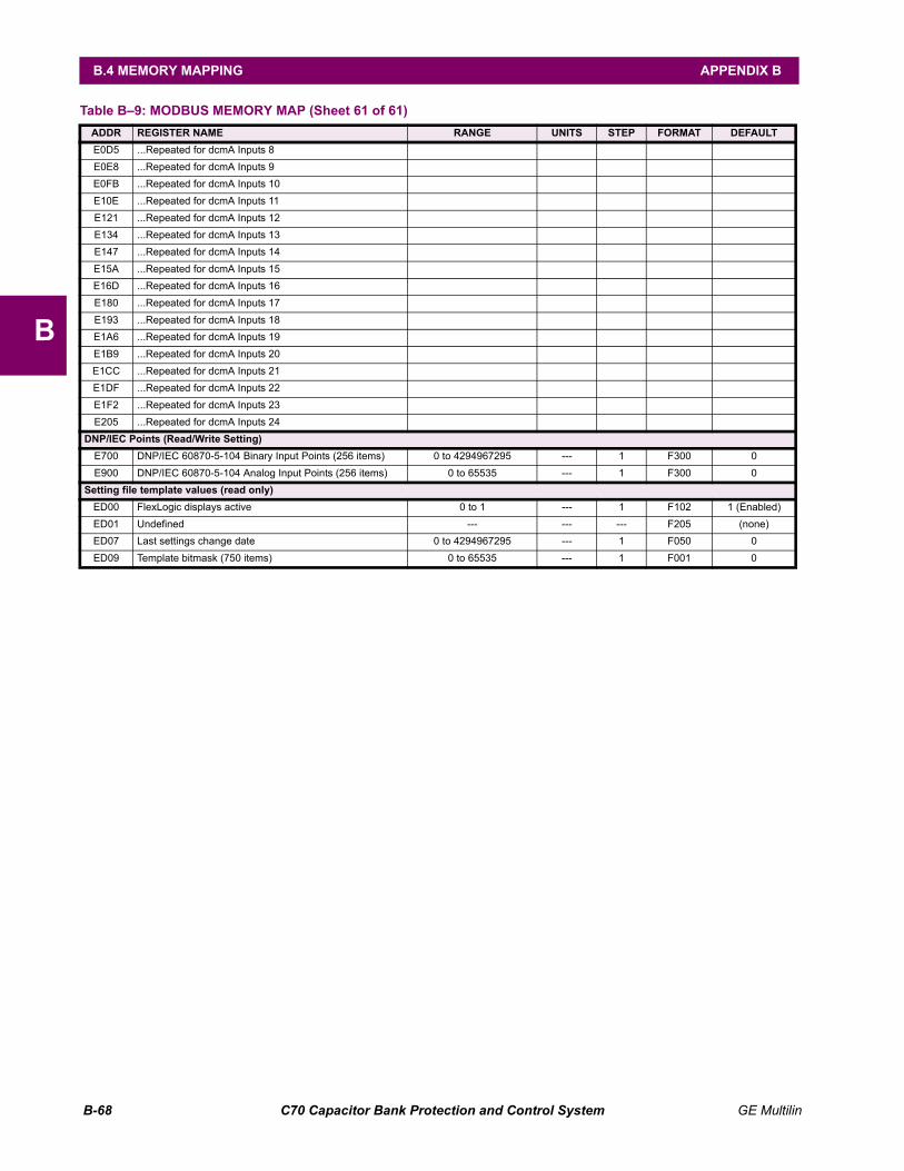
B-68 C70 Capacitor Bank Protection and Control System GE Multilin
B.4 MEMORY MAPPING APPENDIX B
B
E0D5 ...Repeated for dcmA Inputs 8
E0E8 ...Repeated for dcmA Inputs 9
E0FB ...Repeated for dcmA Inputs 10
E10E ...Repeated for dcmA Inputs 11
E121 ...Repeated for dcmA Inputs 12
E134 ...Repeated for dcmA Inputs 13
E147 ...Repeated for dcmA Inputs 14
E15A ...Repeated for dcmA Inputs 15
E16D ...Repeated for dcmA Inputs 16
E180 ...Repeated for dcmA Inputs 17
E193 ...Repeated for dcmA Inputs 18
E1A6 ...Repeated for dcmA Inputs 19
E1B9 ...Repeated for dcmA Inputs 20
E1CC ...Repeated for dcmA Inputs 21
E1DF ...Repeated for dcmA Inputs 22
E1F2 ...Repeated for dcmA Inputs 23
E205 ...Repeated for dcmA Inputs 24
DNP/IEC Points (Read/Write Setting)
E700 DNP/IEC 60870-5-104 Binary Input Points (256 items) 0 to 4294967295 --- 1 F300 0
E900 DNP/IEC 60870-5-104 Analog Input Points (256 items) 0 to 65535 --- 1 F300 0
Setting file template values (read only)
ED00 FlexLogic displays active 0 to 1 --- 1 F102 1 (Enabled)
ED01 Undefined --- --- --- F205 (none)
ED07 Last settings change date 0 to 4294967295 --- 1 F050 0
ED09 Template bitmask (750 items) 0 to 65535 --- 1 F001 0
Table B–9: MODBUS MEMORY MAP (Sheet 61 of 61)
ADDR REGISTER NAME RANGE UNITS STEP FORMAT DEFAULT

GE Multilin C70 Capacitor Bank Protection and Control System B-69
APPENDIX B B.4 MEMORY MAPPING
B
B.4.2 DATA FORMATS
F001UR_UINT16 UNSIGNED 16 BIT INTEGER
F002UR_SINT16 SIGNED 16 BIT INTEGER
F003UR_UINT32 UNSIGNED 32 BIT INTEGER (2 registers)
High order word is stored in the first register.Low order word is stored in the second register.
F004UR_SINT32 SIGNED 32 BIT INTEGER (2 registers)
High order word is stored in the first register/Low order word is stored in the second register.
F005UR_UINT8 UNSIGNED 8 BIT INTEGER
F006UR_SINT8 SIGNED 8 BIT INTEGER
F011UR_UINT16 FLEXCURVE DATA (120 points)
A FlexCurve is an array of 120 consecutive data points (x, y) whichare interpolated to generate a smooth curve. The y-axis is the userdefined trip or operation time setting; the x-axis is the pickup ratioand is pre-defined. Refer to format F119 for a listing of the pickupratios; the enumeration value for the pickup ratio indicates the off-set into the FlexCurve base address where the corresponding timevalue is stored.
F012DISPLAY_SCALE DISPLAY SCALING(unsigned 16-bit integer)
MSB indicates the SI units as a power of ten. LSB indicates thenumber of decimal points to display.
Example: Current values are stored as 32 bit numbers with threedecimal places and base units in Amps. If the retrieved value is12345.678 A and the display scale equals 0x0302 then the dis-played value on the unit is 12.35 kA.
F013POWER_FACTOR (SIGNED 16 BIT INTEGER)
Positive values indicate lagging power factor; negative valuesindicate leading.
F040UR_UINT48 48-BIT UNSIGNED INTEGER
F050UR_UINT32 TIME and DATE (UNSIGNED 32 BIT INTEGER)
Gives the current time in seconds elapsed since 00:00:00 January1, 1970.
F051UR_UINT32 DATE in SR format (alternate format for F050)
First 16 bits are Month/Day (MM/DD/xxxx). Month: 1=January,2=February,...,12=December; Day: 1 to 31 in steps of 1Last 16 bits are Year (xx/xx/YYYY): 1970 to 2106 in steps of 1
F052UR_UINT32 TIME in SR format (alternate format for F050)
First 16 bits are Hours/Minutes (HH:MM:xx.xxx).Hours: 0=12am, 1=1am,...,12=12pm,...23=11pm;Minutes: 0 to 59 in steps of 1
Last 16 bits are Seconds (xx:xx:.SS.SSS): 0=00.000s,1=00.001,...,59999=59.999s)
F060FLOATING_POINT IEEE FLOATING POINT (32 bits)
F070HEX2 2 BYTES - 4 ASCII DIGITS
F071HEX4 4 BYTES - 8 ASCII DIGITS
F072HEX6 6 BYTES - 12 ASCII DIGITS
F073HEX8 8 BYTES - 16 ASCII DIGITS
F074HEX20 20 BYTES - 40 ASCII DIGITS
F083ENUMERATION: SELECTOR MODES
0 = Time-Out, 1 = Acknowledge
F084ENUMERATION: SELECTOR POWER UP
0 = Restore, 1 = Synchronize, 2 = Sync/Restore
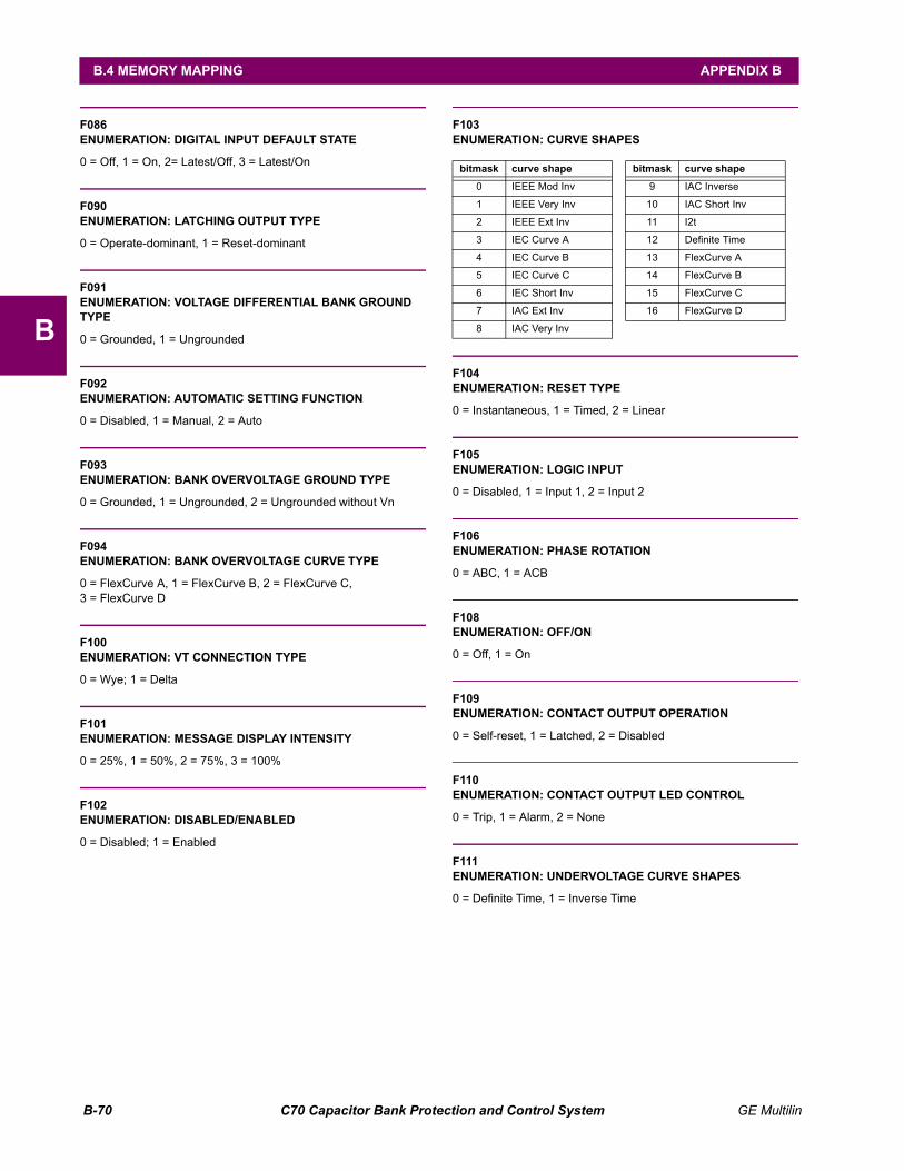
B-70 C70 Capacitor Bank Protection and Control System GE Multilin
B.4 MEMORY MAPPING APPENDIX B
B
F086ENUMERATION: DIGITAL INPUT DEFAULT STATE
0 = Off, 1 = On, 2= Latest/Off, 3 = Latest/On
F090ENUMERATION: LATCHING OUTPUT TYPE
0 = Operate-dominant, 1 = Reset-dominant
F091ENUMERATION: VOLTAGE DIFFERENTIAL BANK GROUNDTYPE
0 = Grounded, 1 = Ungrounded
F092ENUMERATION: AUTOMATIC SETTING FUNCTION
0 = Disabled, 1 = Manual, 2 = Auto
F093ENUMERATION: BANK OVERVOLTAGE GROUND TYPE
0 = Grounded, 1 = Ungrounded, 2 = Ungrounded without Vn
F094ENUMERATION: BANK OVERVOLTAGE CURVE TYPE
0 = FlexCurve A, 1 = FlexCurve B, 2 = FlexCurve C,3 = FlexCurve D
F100ENUMERATION: VT CONNECTION TYPE
0 = Wye; 1 = Delta
F101ENUMERATION: MESSAGE DISPLAY INTENSITY
0 = 25%, 1 = 50%, 2 = 75%, 3 = 100%
F102ENUMERATION: DISABLED/ENABLED
0 = Disabled; 1 = Enabled
F103ENUMERATION: CURVE SHAPES
F104ENUMERATION: RESET TYPE
0 = Instantaneous, 1 = Timed, 2 = Linear
F105ENUMERATION: LOGIC INPUT
0 = Disabled, 1 = Input 1, 2 = Input 2
F106ENUMERATION: PHASE ROTATION
0 = ABC, 1 = ACB
F108ENUMERATION: OFF/ON
0 = Off, 1 = On
F109ENUMERATION: CONTACT OUTPUT OPERATION
0 = Self-reset, 1 = Latched, 2 = Disabled
F110ENUMERATION: CONTACT OUTPUT LED CONTROL
0 = Trip, 1 = Alarm, 2 = None
F111ENUMERATION: UNDERVOLTAGE CURVE SHAPES
0 = Definite Time, 1 = Inverse Time
bitmask curve shape bitmask curve shape
0 IEEE Mod Inv 9 IAC Inverse
1 IEEE Very Inv 10 IAC Short Inv
2 IEEE Ext Inv 11 I2t
3 IEC Curve A 12 Definite Time
4 IEC Curve B 13 FlexCurve A
5 IEC Curve C 14 FlexCurve B
6 IEC Short Inv 15 FlexCurve C
7 IAC Ext Inv 16 FlexCurve D
8 IAC Very Inv

GE Multilin C70 Capacitor Bank Protection and Control System B-71
APPENDIX B B.4 MEMORY MAPPING
B
F112ENUMERATION: RS485 BAUD RATES
F113ENUMERATION: PARITY
0 = None, 1 = Odd, 2 = Even
F114ENUMERATION: IRIG-B SIGNAL TYPE
0 = None, 1 = DC Shift, 2 = Amplitude Modulated
F115ENUMERATION: BREAKER STATUS
0 = Auxiliary A, 1 = Auxiliary B
F116ENUMERATION: NEUTRAL OVERVOLTAGE CURVES
0 = Definite Time, 1 = FlexCurve A, 2 = FlexCurve B,3 = FlexCurve C
F117ENUMERATION: NUMBER OF OSCILLOGRAPHY RECORDS
0 = 172 cycles, 1 = 336 cycles, 2 = 718 cycles, 3 = 159 cycles
F118ENUMERATION: OSCILLOGRAPHY MODE
0 = Automatic Overwrite, 1 = Protected
F119ENUMERATION: FLEXCURVE PICKUP RATIOS
F122ENUMERATION: ELEMENT INPUT SIGNAL TYPE
0 = Phasor, 1 = RMS
F123ENUMERATION: CT SECONDARY
0 = 1 A, 1 = 5 A
F124ENUMERATION: LIST OF ELEMENTS
bitmask value bitmask value bitmask value
0 300 4 9600 8 115200
1 1200 5 19200 9 14400
2 2400 6 38400 10 28800
3 4800 7 57600 11 33600
mask value mask value mask value mask value
0 0.00 30 0.88 60 2.90 90 5.90
1 0.05 31 0.90 61 3.00 91 6.00
2 0.10 32 0.91 62 3.10 92 6.50
3 0.15 33 0.92 63 3.20 93 7.00
4 0.20 34 0.93 64 3.30 94 7.50
5 0.25 35 0.94 65 3.40 95 8.00
6 0.30 36 0.95 66 3.50 96 8.50
7 0.35 37 0.96 67 3.60 97 9.00
8 0.40 38 0.97 68 3.70 98 9.50
9 0.45 39 0.98 69 3.80 99 10.00
10 0.48 40 1.03 70 3.90 100 10.50
11 0.50 41 1.05 71 4.00 101 11.00
12 0.52 42 1.10 72 4.10 102 11.50
13 0.54 43 1.20 73 4.20 103 12.00
14 0.56 44 1.30 74 4.30 104 12.50
15 0.58 45 1.40 75 4.40 105 13.00
16 0.60 46 1.50 76 4.50 106 13.50
17 0.62 47 1.60 77 4.60 107 14.00
18 0.64 48 1.70 78 4.70 108 14.50
19 0.66 49 1.80 79 4.80 109 15.00
20 0.68 50 1.90 80 4.90 110 15.50
21 0.70 51 2.00 81 5.00 111 16.00
22 0.72 52 2.10 82 5.10 112 16.50
23 0.74 53 2.20 83 5.20 113 17.00
24 0.76 54 2.30 84 5.30 114 17.50
25 0.78 55 2.40 85 5.40 115 18.00
26 0.80 56 2.50 86 5.50 116 18.50
27 0.82 57 2.60 87 5.60 117 19.00
28 0.84 58 2.70 88 5.70 118 19.50
29 0.86 59 2.80 89 5.80 119 20.00
bitmask element
0 Phase Instantaneous Overcurrent 1
1 Phase Instantaneous Overcurrent 2
2 Phase Instantaneous Overcurrent 3
3 Phase Instantaneous Overcurrent 4
4 Phase Instantaneous Overcurrent 5

B-72 C70 Capacitor Bank Protection and Control System GE Multilin
B.4 MEMORY MAPPING APPENDIX B
B
5 Phase Instantaneous Overcurrent 6
6 Phase Instantaneous Overcurrent 7
7 Phase Instantaneous Overcurrent 8
8 Phase Instantaneous Overcurrent 9
9 Phase Instantaneous Overcurrent 10
10 Phase Instantaneous Overcurrent 11
11 Phase Instantaneous Overcurrent 12
16 Phase Time Overcurrent 1
17 Phase Time Overcurrent 2
18 Phase Time Overcurrent 3
19 Phase Time Overcurrent 4
20 Phase Time Overcurrent 5
21 Phase Time Overcurrent 6
24 Phase Directional Overcurrent 1
25 Phase Directional Overcurrent 2
32 Neutral Instantaneous Overcurrent 1
33 Neutral Instantaneous Overcurrent 2
34 Neutral Instantaneous Overcurrent 3
35 Neutral Instantaneous Overcurrent 4
36 Neutral Instantaneous Overcurrent 5
37 Neutral Instantaneous Overcurrent 6
38 Neutral Instantaneous Overcurrent 7
39 Neutral Instantaneous Overcurrent 8
40 Neutral Instantaneous Overcurrent 9
41 Neutral Instantaneous Overcurrent 10
42 Neutral Instantaneous Overcurrent 11
43 Neutral Instantaneous Overcurrent 12
48 Neutral Time Overcurrent 1
49 Neutral Time Overcurrent 2
50 Neutral Time Overcurrent 3
51 Neutral Time Overcurrent 4
52 Neutral Time Overcurrent 5
53 Neutral Time Overcurrent 6
56 Neutral Directional Overcurrent 1
60 Negative Sequence Directional Overcurrent 1
61 Negative Sequence Directional Overcurrent 2
64 Ground Instantaneous Overcurrent 1
65 Ground Instantaneous Overcurrent 2
66 Ground Instantaneous Overcurrent 3
67 Ground Instantaneous Overcurrent 4
68 Ground Instantaneous Overcurrent 5
69 Ground Instantaneous Overcurrent 6
70 Ground Instantaneous Overcurrent 7
71 Ground Instantaneous Overcurrent 8
72 Ground Instantaneous Overcurrent 9
73 Ground Instantaneous Overcurrent 10
74 Ground Instantaneous Overcurrent 11
75 Ground Instantaneous Overcurrent 12
80 Ground Time Overcurrent 1
81 Ground Time Overcurrent 2
82 Ground Time Overcurrent 3
83 Ground Time Overcurrent 4
84 Ground Time Overcurrent 5
bitmask element
85 Ground Time Overcurrent 6
96 Negative Sequence Instantaneous Overcurrent 1
97 Negative Sequence Instantaneous Overcurrent 2
112 Negative Sequence Time Overcurrent 1
113 Negative Sequence Time Overcurrent 2
120 Negative Sequence Overvoltage
144 Phase Undervoltage 1
145 Phase Undervoltage 2
148 Auxiliary Overvoltage 1
152 Phase Overvoltage 1
154 Compensated Overvoltage 1
156 Neutral Overvoltage 1
224 SRC1 VT Fuse Failure
225 SRC2 VT Fuse Failure
226 SRC3 VT Fuse Failure
227 SRC4 VT Fuse Failure
228 SRC5 VT Fuse Failure
229 SRC6 VT Fuse Failure
232 SRC1 50DD (Disturbance Detection)
233 SRC2 50DD (Disturbance Detection)
234 SRC3 50DD (Disturbance Detection)
235 SRC4 50DD (Disturbance Detection)
236 SRC5 50DD (Disturbance Detection)
237 SRC6 50DD (Disturbance Detection)
280 Breaker Failure 1
281 Breaker Failure 2
282 Breaker Failure 3
283 Breaker Failure 4
284 Breaker Failure 5
285 Breaker Failure 6
294 Breaker 1 Flashover
295 Breaker 2 Flashover
336 Setting Group
337 Reset
340 Neutral voltage unbalance 1
341 Neutral voltage unbalance 2
342 Neutral voltage unbalance 3
388 Selector 1
389 Selector 2
390 Control pushbutton 1
391 Control pushbutton 2
392 Control pushbutton 3
393 Control pushbutton 4
394 Control pushbutton 5
395 Control pushbutton 6
396 Control pushbutton 7
400 FlexElement 1
401 FlexElement 2
402 FlexElement 3
403 FlexElement 4
404 FlexElement 5
405 FlexElement 6
406 FlexElemen 7
bitmask element
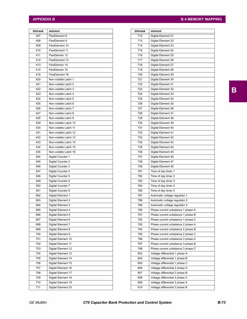
GE Multilin C70 Capacitor Bank Protection and Control System B-73
APPENDIX B B.4 MEMORY MAPPING
B
407 FlexElement 8
408 FlexElement 9
409 FlexElement 10
410 FlexElement 11
411 FlexElemen 12
412 FlexElement 13
413 FlexElemen 14
414 FlexElemen 15
415 FlexElement 16
420 Non-volatile Latch 1
421 Non-volatile Latch 2
422 Non-volatile Latch 3
423 Non-volatile Latch 4
424 Non-volatile Latch 5
425 Non-volatile Latch 6
426 Non-volatile Latch 7
427 Non-volatile Latch 8
428 Non-volatile Latch 9
429 Non-volatile Latch 10
430 Non-volatile Latch 11
431 Non-volatile Latch 12
432 Non-volatile Latch 13
433 Non-volatile Latch 14
434 Non-volatile Latch 15
435 Non-volatile Latch 16
544 Digital Counter 1
545 Digital Counter 2
546 Digital Counter 3
547 Digital Counter 4
548 Digital Counter 5
549 Digital Counter 6
550 Digital Counter 7
551 Digital Counter 8
692 Digital Element 1
693 Digital Element 2
694 Digital Element 3
695 Digital Element 4
696 Digital Element 5
697 Digital Element 6
698 Digital Element 7
699 Digital Element 8
700 Digital Element 9
701 Digital Element 10
702 Digital Element 11
703 Digital Element 12
704 Digital Element 13
705 Digital Element 14
706 Digital Element 15
707 Digital Element 16
708 Digital Element 17
709 Digital Element 18
710 Digital Element 19
711 Digital Element 20
bitmask element
712 Digital Element 21
713 Digital Element 22
714 Digital Element 23
715 Digital Element 24
716 Digital Element 25
717 Digital Element 26
718 Digital Element 27
719 Digital Element 28
720 Digital Element 29
721 Digital Element 30
722 Digital Element 31
723 Digital Element 32
724 Digital Element 33
725 Digital Element 34
726 Digital Element 35
727 Digital Element 36
728 Digital Element 37
729 Digital Element 38
730 Digital Element 39
731 Digital Element 40
732 Digital Element 41
733 Digital Element 42
734 Digital Element 43
735 Digital Element 44
736 Digital Element 45
737 Digital Element 46
738 Digital Element 47
739 Digital Element 48
781 Time of day timer 1
782 Time of day timer 2
783 Time of day timer 3
784 Time of day timer 4
785 Time of day timer 5
787 Automatic voltage regulator 1
788 Automatic voltage regulator 2
789 Automatic voltage regulator 3
790 Phase current unbalance 1 phase A
791 Phase current unbalance 1 phase B
792 Phase current unbalance 1 phase C
793 Phase current unbalance 2 phase A
794 Phase current unbalance 2 phase B
795 Phase current unbalance 2 phase C
796 Phase current unbalance 3 phase A
797 Phase current unbalance 3 phase B
798 Phase current unbalance 3 phase C
803 Voltage differential 1 phase A
804 Voltage differential 1 phase B
805 Voltage differential 1 phase C
806 Voltage differential 2 phase A
807 Voltage differential 2 phase B
808 Voltage differential 2 phase C
809 Voltage differential 3 phase A
810 Voltage differential 3 phase B
bitmask element

B-74 C70 Capacitor Bank Protection and Control System GE Multilin
B.4 MEMORY MAPPING APPENDIX B
B
811 Voltage differential 3 phase C
813 Capacitor control 1
814 Capacitor control 2
815 Capacitor control 3
816 Capacitor control 4
820 Neutral current unbalance 1
821 Neutral current unbalance 2
822 Neutral current unbalance 3
830 Bank phase overvoltage 1 phase A
831 Bank phase overvoltage 1 phase B
832 Bank phase overvoltage 1 phase C
833 Bank phase overvoltage 2 phase A
834 Bank phase overvoltage 2 phase B
835 Bank phase overvoltage 2 phase C
842 Trip Bus 1
843 Trip Bus 2
844 Trip Bus 3
845 Trip Bus 4
846 Trip Bus 5
847 Trip Bus 6
849 RTD Input 1
850 RTD Input 2
851 RTD Input 3
852 RTD Input 4
853 RTD Input 5
854 RTD Input 6
855 RTD Input 7
856 RTD Input 8
857 RTD Input 9
858 RTD Input 10
859 RTD Input 11
860 RTD Input 12
861 RTD Input 13
862 RTD Input 14
863 RTD Input 15
864 RTD Input 16
865 RTD Input 17
866 RTD Input 18
867 RTD Input 19
868 RTD Input 20
869 RTD Input 21
870 RTD Input 22
871 RTD Input 23
872 RTD Input 24
873 RTD Input 25
874 RTD Input 26
875 RTD Input 27
876 RTD Input 28
877 RTD Input 29
878 RTD Input 30
879 RTD Input 31
880 RTD Input 32
881 RTD Input 33
bitmask element
882 RTD Input 34
883 RTD Input 35
884 RTD Input 36
885 RTD Input 37
886 RTD Input 38
887 RTD Input 39
888 RTD Input 40
889 RTD Input 41
890 RTD Input 42
891 RTD Input 43
892 RTD Input 44
893 RTD Input 45
894 RTD Input 46
895 RTD Input 47
896 RTD Input 48
900 User-Programmable Pushbutton 1
901 User-Programmable Pushbutton 2
902 User-Programmable Pushbutton 3
903 User-Programmable Pushbutton 4
904 User-Programmable Pushbutton 5
905 User-Programmable Pushbutton 6
906 User-Programmable Pushbutton 7
907 User-Programmable Pushbutton 8
908 User-Programmable Pushbutton 9
909 User-Programmable Pushbutton 10
910 User-Programmable Pushbutton 11
911 User-Programmable Pushbutton 12
912 User-Programmable Pushbutton 13
913 User-Programmable Pushbutton 14
914 User-Programmable Pushbutton 15
915 User-Programmable Pushbutton 16
920 Disconnect switch 1
921 Disconnect switch 2
922 Disconnect switch 3
923 Disconnect switch 4
924 Disconnect switch 5
925 Disconnect switch 6
926 Disconnect switch 7
927 Disconnect switch 8
928 Disconnect switch 9
929 Disconnect switch 10
930 Disconnect switch 11
931 Disconnect switch 12
932 Disconnect switch 13
933 Disconnect switch 14
934 Disconnect switch 15
935 Disconnect switch 16
936 Disconnect switch 17
937 Disconnect switch 18
938 Disconnect switch 19
939 Disconnect switch 20
940 Disconnect switch 21
941 Disconnect switch 22
bitmask element
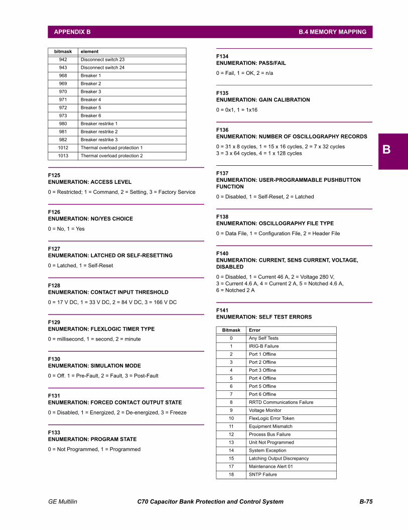
GE Multilin C70 Capacitor Bank Protection and Control System B-75
APPENDIX B B.4 MEMORY MAPPING
B
F125ENUMERATION: ACCESS LEVEL
0 = Restricted; 1 = Command, 2 = Setting, 3 = Factory Service
F126ENUMERATION: NO/YES CHOICE
0 = No, 1 = Yes
F127ENUMERATION: LATCHED OR SELF-RESETTING
0 = Latched, 1 = Self-Reset
F128ENUMERATION: CONTACT INPUT THRESHOLD
0 = 17 V DC, 1 = 33 V DC, 2 = 84 V DC, 3 = 166 V DC
F129ENUMERATION: FLEXLOGIC TIMER TYPE
0 = millisecond, 1 = second, 2 = minute
F130ENUMERATION: SIMULATION MODE
0 = Off. 1 = Pre-Fault, 2 = Fault, 3 = Post-Fault
F131ENUMERATION: FORCED CONTACT OUTPUT STATE
0 = Disabled, 1 = Energized, 2 = De-energized, 3 = Freeze
F133ENUMERATION: PROGRAM STATE
0 = Not Programmed, 1 = Programmed
F134ENUMERATION: PASS/FAIL
0 = Fail, 1 = OK, 2 = n/a
F135ENUMERATION: GAIN CALIBRATION
0 = 0x1, 1 = 1x16
F136ENUMERATION: NUMBER OF OSCILLOGRAPHY RECORDS
0 = 31 x 8 cycles, 1 = 15 x 16 cycles, 2 = 7 x 32 cycles3 = 3 x 64 cycles, 4 = 1 x 128 cycles
F137ENUMERATION: USER-PROGRAMMABLE PUSHBUTTONFUNCTION
0 = Disabled, 1 = Self-Reset, 2 = Latched
F138ENUMERATION: OSCILLOGRAPHY FILE TYPE
0 = Data File, 1 = Configuration File, 2 = Header File
F140ENUMERATION: CURRENT, SENS CURRENT, VOLTAGE,DISABLED
0 = Disabled, 1 = Current 46 A, 2 = Voltage 280 V,3 = Current 4.6 A, 4 = Current 2 A, 5 = Notched 4.6 A,6 = Notched 2 A
F141ENUMERATION: SELF TEST ERRORS
942 Disconnect switch 23
943 Disconnect switch 24
968 Breaker 1
969 Breaker 2
970 Breaker 3
971 Breaker 4
972 Breaker 5
973 Breaker 6
980 Breaker restrike 1
981 Breaker restrike 2
982 Breaker restrike 3
1012 Thermal overload protection 1
1013 Thermal overload protection 2
bitmask element
Bitmask Error
0 Any Self Tests
1 IRIG-B Failure
2 Port 1 Offline
3 Port 2 Offline
4 Port 3 Offline
5 Port 4 Offline
6 Port 5 Offline
7 Port 6 Offline
8 RRTD Communications Failure
9 Voltage Monitor
10 FlexLogic Error Token
11 Equipment Mismatch
12 Process Bus Failure
13 Unit Not Programmed
14 System Exception
15 Latching Output Discrepancy
17 Maintenance Alert 01
18 SNTP Failure

B-76 C70 Capacitor Bank Protection and Control System GE Multilin
B.4 MEMORY MAPPING APPENDIX B
B
F142ENUMERATION: EVENT RECORDER ACCESS FILE TYPE
0 = All Record Data, 1 = Headers Only, 2 = Numeric Event Cause
F143UR_UINT32: 32 BIT ERROR CODE (F141 specifies bit number)
A bit value of 0 = no error, 1 = error
F144ENUMERATION: FORCED CONTACT INPUT STATE
0 = Disabled, 1 = Open, 2 = Closed
F145ENUMERATION: ALPHABET LETTER
F146ENUMERATION: MISCELLANEOUS EVENT CAUSES
19 Maintenance Alert
20 Maintenance Alert
21 Maintenance Alert
22 Temperature Monitor
23 Process Bus Trouble
24 Brick Trouble
25 Field RTD Trouble
26 Field TDR Trouble
27 Remote Device Offline
28 Direct Device Offline
29 Maintenance Alert
30 Any Minor Error
31 Any Major Error
33 Maintenance Alert
64 Maintenance Alert
65 IEC 61850 Data Set
66 Aggregator Error
67 Unit Not Calibrated
68 Settings Save Error
69 SRAM Data Error
70 Program Memory
71 Watchdog Error
72 Low On Memory
73 Prototype Firmware
74 Module Failure 01
75 Module Failure 02
76 Module Failure 03
77 Module Failure 04
78 Module Failure 05
79 Module Failure 06
80 Module Failure 07
81 Module Failure 08
82 Module Failure 09
83 Incompatible H/W
84 Module Failure 10
85 Module Failure 11
86 Module Failure 12
87 High ENET Traffic
89 Relay Restart
90 FGM Failure
91 FGM Failure
92 FGM Failure
93 FGM Failure
94 FGM Failure
95 FGM Error
96 Maintenance Alert
97 PHY Monitor
98 Storage Media Alarm
99 Wrong Transceiver
Bitmask Error
bitmask type bitmask type bitmask type bitmask type
0 null 7 G 14 N 21 U
1 A 8 H 15 O 22 V
2 B 9 I 16 P 23 W
3 C 10 J 17 Q 24 X
4 D 11 K 18 R 25 Y
5 E 12 L 19 S 26 Z
6 F 13 M 20 T
bitmask definition
0 Events Cleared
1 Oscillography Triggered
2 Date/time Changed
3 Default Settings Loaded
4 Test Mode Forcing On
5 Test Mode Forcing Off
6 Power On
7 Power Off
8 Relay In Service
9 Relay Out Of Service
10 Watchdog Reset
11 Oscillography Clear
12 Reboot Command
13 Led Test Initiated
14 Flash Programming
15 Fault Report Trigger
16 User Programmable Fault Report Trigger
17 ---
18 Reload CT/VT module Settings
19 ---
20 Ethernet Port 1 Offline
21 Ethernet Port 2 Offline
22 Ethernet Port 3 Offline
23 Ethernet Port 4 Offline

GE Multilin C70 Capacitor Bank Protection and Control System B-77
APPENDIX B B.4 MEMORY MAPPING
BF151ENUMERATION: RTD SELECTION
F152ENUMERATION: SETTING GROUP
0 = Active Group, 1 = Group 1, 2 = Group 2, 3 = Group 34 = Group 4, 5 = Group 5, 6 = Group 6
F155ENUMERATION: REMOTE DEVICE STATE
0 = Offline, 1 = Online
F156ENUMERATION: REMOTE INPUT BIT PAIRS
F157ENUMERATION: BREAKER MODE
0 = 3-Pole, 1 = 1-Pole
F159ENUMERATION: BREAKER AUX CONTACT KEYING
0 = 52a, 1 = 52b, 2 = None
F166ENUMERATION: AUXILIARY VT CONNECTION TYPE
0 = Vn, 1 = Vag, 2 = Vbg, 3 = Vcg, 4 = Vab, 5 = Vbc, 6 = Vca
24 Ethernet Port 5 Offline
25 Ethernet Port 6 Offline
26 Test Mode Isolated
27 Test Mode Forcible
28 Test Mode Disabled
29 Temperature Warning On
30 Temperature Warning Off
31 Unauthorized Access
32 System Integrity Recovery
33 System Integrity Recovery 06
34 System Integrity Recovery 07
bitmask RTD# bitmask RTD# bitmask RTD#
0 NONE 17 RTD 17 33 RTD 33
1 RTD 1 18 RTD 18 34 RTD 34
2 RTD 2 19 RTD 19 35 RTD 35
3 RTD 3 20 RTD 20 36 RTD 36
4 RTD 4 21 RTD 21 37 RTD 37
5 RTD 5 22 RTD 22 38 RTD 38
6 RTD 6 23 RTD 23 39 RTD 39
7 RTD 7 24 RTD 24 40 RTD 40
8 RTD 8 25 RTD 25 41 RTD 41
9 RTD 9 26 RTD 26 42 RTD 42
10 RTD 10 27 RTD 27 43 RTD 43
11 RTD 11 28 RTD 28 44 RTD 44
12 RTD 12 29 RTD 29 45 RTD 45
13 RTD 13 30 RTD 30 46 RTD 46
14 RTD 14 31 RTD 31 47 RTD 47
15 RTD 15 32 RTD 32 48 RTD 48
16 RTD 16
bitmask definition
bitmask value bitmask value
0 NONE 35 UserSt-3
1 DNA-1 36 UserSt-4
2 DNA-2 37 UserSt-5
3 DNA-3 38 UserSt-6
4 DNA-4 39 UserSt-7
5 DNA-5 40 UserSt-8
6 DNA-6 41 UserSt-9
7 DNA-7 42 UserSt-10
8 DNA-8 43 UserSt-11
9 DNA-9 44 UserSt-12
10 DNA-10 45 UserSt-13
11 DNA-11 46 UserSt-14
12 DNA-12 47 UserSt-15
13 DNA-13 48 UserSt-16
14 DNA-14 49 UserSt-17
15 DNA-15 50 UserSt-18
16 DNA-16 51 UserSt-19
17 DNA-17 52 UserSt-20
18 DNA-18 53 UserSt-21
19 DNA-19 54 UserSt-22
20 DNA-20 55 UserSt-23
21 DNA-21 56 UserSt-24
22 DNA-22 57 UserSt-25
23 DNA-23 58 UserSt-26
24 DNA-24 59 UserSt-27
25 DNA-25 60 UserSt-28
26 DNA-26 61 UserSt-29
27 DNA-27 62 UserSt-30
28 DNA-28 63 UserSt-31
29 DNA-29 64 UserSt-32
30 DNA-30 65 Dataset Item 1
31 DNA-31 66 Dataset Item 2
32 DNA-32 67 Dataset Item 3
33 UserSt-1
34 UserSt-2 96 Dataset Item 32

B-78 C70 Capacitor Bank Protection and Control System GE Multilin
B.4 MEMORY MAPPING APPENDIX B
B
F167ENUMERATION: SIGNAL SOURCE
0 = SRC 1, 1 = SRC 2, 2 = SRC 3, 3 = SRC 4,4 = SRC 5, 5 = SRC 6
F168ENUMERATION: INRUSH INHIBIT FUNCTION
0 = Disabled, 1 = Adapt. 2nd, 2 = Trad. 2nd
F170ENUMERATION: LOW/HIGH OFFSET and GAINTRANSDUCER INPUT/OUTPUT SELECTION
0 = LOW, 1 = HIGH
F171ENUMERATION: TRANSDUCER CHANNEL INPUT TYPE
0 = dcmA IN, 1 = Ohms IN, 2 = RTD IN, 3 = dcmA OUT,4 = RRTD IN
F172ENUMERATION: SLOT LETTERS
F173ENUMERATION: DCMA INPUT/OUTPUT RANGE
F174ENUMERATION: TRANSDUCER RTD INPUT TYPE
0 = 100 Ohm Platinum, 1 = 120 Ohm Nickel,2 = 100 Ohm Nickel, 3 = 10 Ohm Copper
F175ENUMERATION: PHASE LETTERS
0 = A, 1 = B, 2 = C
F177ENUMERATION: COMMUNICATION PORT
0 = None, 1 = COM1-RS485 (not applicable to UR firmware 7.00),2 = COM2-RS485, 3 = Front Panel-RS232, 4 = Network - TCP, 5 = Network - UDP
F178ENUMERATION: DATA LOGGER RATES
0 = 1 sec, 1 = 1 min, 2 = 5 min, 3 = 10 min, 4 = 15 min,5 = 20 min, 6 = 30 min, 7 = 60 min, 8 = 15 ms, 9 = 30 ms,10 = 100 ms, 11 = 500 ms
F179ENUMERATION: NEGATIVE SEQUENCE DIRECTIONALOVERCURRENT TYPE
0 = Neg Sequence, 1 = Zero Sequence
F180ENUMERATION: PHASE/GROUND
0 = PHASE, 1 = GROUND
F181ENUMERATION: ODD/EVEN/NONE
0 = ODD, 1 = EVEN, 2 = NONE
F183ENUMERATION: AC INPUT WAVEFORMS
F184ENUMERATION: REMOTE DEVICE GOOSE DATASET
bitmask slot bitmask slot bitmask slot bitmask slot
0 F 4 K 8 P 12 U
1 G 5 L 9 R 13 V
2 H 6 M 10 S 14 W
3 J 7 N 11 T 15 X
bitmask dcmA input/output range
0 0 to –1 mA
1 0 to 1 mA
2 –1 to 1 mA
3 0 to 5 mA
4 0 to 10 mA
5 0 to 20 mA
6 4 to 20 mA
bitmask definition
0 Off
1 8 samples/cycle
2 16 samples/cycle
3 32 samples/cycle
4 64 samples/cycle
value GOOSE dataset
0 Off
1 GooseIn 1
2 GooseIn 2
3 GooseIn 3
4 GooseIn 4
5 GooseIn 5
6 GooseIn 6
7 GooseIn 7
8 GooseIn 8
9 GooseIn 9
10 GooseIn 10
11 GooseIn 11
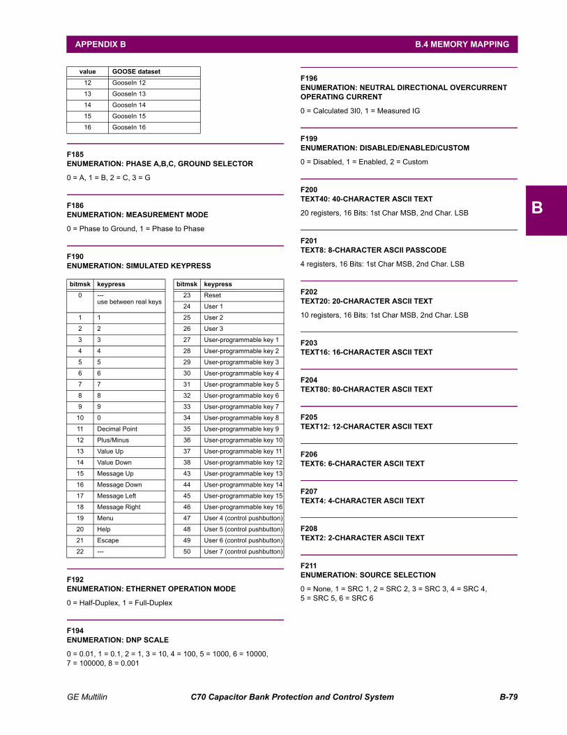
GE Multilin C70 Capacitor Bank Protection and Control System B-79
APPENDIX B B.4 MEMORY MAPPING
B
F185ENUMERATION: PHASE A,B,C, GROUND SELECTOR
0 = A, 1 = B, 2 = C, 3 = G
F186ENUMERATION: MEASUREMENT MODE
0 = Phase to Ground, 1 = Phase to Phase
F190ENUMERATION: SIMULATED KEYPRESS
F192ENUMERATION: ETHERNET OPERATION MODE
0 = Half-Duplex, 1 = Full-Duplex
F194ENUMERATION: DNP SCALE
0 = 0.01, 1 = 0.1, 2 = 1, 3 = 10, 4 = 100, 5 = 1000, 6 = 10000,7 = 100000, 8 = 0.001
F196ENUMERATION: NEUTRAL DIRECTIONAL OVERCURRENTOPERATING CURRENT
0 = Calculated 3I0, 1 = Measured IG
F199ENUMERATION: DISABLED/ENABLED/CUSTOM
0 = Disabled, 1 = Enabled, 2 = Custom
F200TEXT40: 40-CHARACTER ASCII TEXT
20 registers, 16 Bits: 1st Char MSB, 2nd Char. LSB
F201TEXT8: 8-CHARACTER ASCII PASSCODE
4 registers, 16 Bits: 1st Char MSB, 2nd Char. LSB
F202TEXT20: 20-CHARACTER ASCII TEXT
10 registers, 16 Bits: 1st Char MSB, 2nd Char. LSB
F203TEXT16: 16-CHARACTER ASCII TEXT
F204TEXT80: 80-CHARACTER ASCII TEXT
F205TEXT12: 12-CHARACTER ASCII TEXT
F206TEXT6: 6-CHARACTER ASCII TEXT
F207TEXT4: 4-CHARACTER ASCII TEXT
F208TEXT2: 2-CHARACTER ASCII TEXT
F211ENUMERATION: SOURCE SELECTION
0 = None, 1 = SRC 1, 2 = SRC 2, 3 = SRC 3, 4 = SRC 4,5 = SRC 5, 6 = SRC 6
12 GooseIn 12
13 GooseIn 13
14 GooseIn 14
15 GooseIn 15
16 GooseIn 16
bitmsk keypress bitmsk keypress
0 ---use between real keys
23 Reset
24 User 1
1 1 25 User 2
2 2 26 User 3
3 3 27 User-programmable key 1
4 4 28 User-programmable key 2
5 5 29 User-programmable key 3
6 6 30 User-programmable key 4
7 7 31 User-programmable key 5
8 8 32 User-programmable key 6
9 9 33 User-programmable key 7
10 0 34 User-programmable key 8
11 Decimal Point 35 User-programmable key 9
12 Plus/Minus 36 User-programmable key 10
13 Value Up 37 User-programmable key 11
14 Value Down 38 User-programmable key 12
15 Message Up 43 User-programmable key 13
16 Message Down 44 User-programmable key 14
17 Message Left 45 User-programmable key 15
18 Message Right 46 User-programmable key 16
19 Menu 47 User 4 (control pushbutton)
20 Help 48 User 5 (control pushbutton)
21 Escape 49 User 6 (control pushbutton)
22 --- 50 User 7 (control pushbutton)
value GOOSE dataset
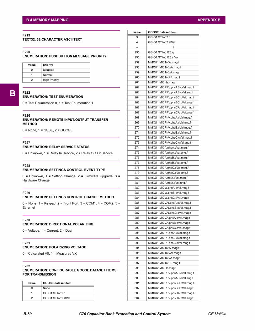
B-80 C70 Capacitor Bank Protection and Control System GE Multilin
B.4 MEMORY MAPPING APPENDIX B
B
F213TEXT32: 32-CHARACTER ASCII TEXT
F220ENUMERATION: PUSHBUTTON MESSAGE PRIORITY
F222ENUMERATION: TEST ENUMERATION
0 = Test Enumeration 0, 1 = Test Enumeration 1
F226ENUMERATION: REMOTE INPUT/OUTPUT TRANSFERMETHOD
0 = None, 1 = GSSE, 2 = GOOSE
F227ENUMERATION: RELAY SERVICE STATUS
0 = Unknown, 1 = Relay In Service, 2 = Relay Out Of Service
F228ENUMERATION: SETTINGS CONTROL EVENT TYPE
0 = Unknown, 1 = Setting Change, 2 = Firmware Upgrade, 3 =Hardware Change
F229ENUMERATION: SETTINGS CONTROL CHANGE METHOD
0 = None, 1 = Keypad, 2 = Front Port, 3 = COM1, 4 = COM2, 5 =Ethernet
F230ENUMERATION: DIRECTIONAL POLARIZING
0 = Voltage, 1 = Current, 2 = Dual
F231ENUMERATION: POLARIZING VOLTAGE
0 = Calculated V0, 1 = Measured VX
F232ENUMERATION: CONFIGURABLE GOOSE DATASET ITEMSFOR TRANSMISSION
value priority
0 Disabled
1 Normal
2 High Priority
value GOOSE dataset item
0 None
1 GGIO1.ST.Ind1.q
2 GGIO1.ST.Ind1.stVal
3 GGIO1.ST.Ind2.q
4 GGIO1.ST.Ind2.stVal
255 GGIO1.ST.Ind128.q
256 GGIO1.ST.Ind128.stVal
257 MMXU1.MX.TotW.mag.f
258 MMXU1.MX.TotVAr.mag.f
259 MMXU1.MX.TotVA.mag.f
260 MMXU1.MX.TotPF.mag.f
261 MMXU1.MX.Hz.mag.f
262 MMXU1.MX.PPV.phsAB.cVal.mag.f
263 MMXU1.MX.PPV.phsAB.cVal.ang.f
264 MMXU1.MX.PPV.phsBC.cVal.mag.f
265 MMXU1.MX.PPV.phsBC.cVal.ang.f
266 MMXU1.MX.PPV.phsCA.cVal.mag.f
267 MMXU1.MX.PPV.phsCA.cVal.ang.f
268 MMXU1.MX.PhV.phsA.cVal.mag.f
269 MMXU1.MX.PhV.phsA.cVal.ang.f
270 MMXU1.MX.PhV.phsB.cVal.mag.f
271 MMXU1.MX.PhV.phsB.cVal.ang.f
272 MMXU1.MX.PhV.phsC.cVal.mag.f
273 MMXU1.MX.PhV.phsC.cVal.ang.f
274 MMXU1.MX.A.phsA.cVal.mag.f
275 MMXU1.MX.A.phsA.cVal.ang.f
276 MMXU1.MX.A.phsB.cVal.mag.f
277 MMXU1.MX.A.phsB.cVal.ang.f
278 MMXU1.MX.A.phsC.cVal.mag.f
279 MMXU1.MX.A.phsC.cVal.ang.f
280 MMXU1.MX.A.neut.cVal.mag.f
281 MMXU1.MX.A.neut.cVal.ang.f
282 MMXU1.MX.W.phsA.cVal.mag.f
283 MMXU1.MX.W.phsB.cVal.mag.f
284 MMXU1.MX.W.phsC.cVal.mag.f
285 MMXU1.MX.VAr.phsA.cVal.mag.f
286 MMXU1.MX.VAr.phsB.cVal.mag.f
287 MMXU1.MX.VAr.phsC.cVal.mag.f
288 MMXU1.MX.VA.phsA.cVal.mag.f
289 MMXU1.MX.VA.phsB.cVal.mag.f
290 MMXU1.MX.VA.phsC.cVal.mag.f
291 MMXU1.MX.PF.phsA.cVal.mag.f
292 MMXU1.MX.PF.phsB.cVal.mag.f
293 MMXU1.MX.PF.phsC.cVal.mag.f
294 MMXU2.MX.TotW.mag.f
295 MMXU2.MX.TotVAr.mag.f
296 MMXU2.MX.TotVA.mag.f
297 MMXU2.MX.TotPF.mag.f
298 MMXU2.MX.Hz.mag.f
299 MMXU2.MX.PPV.phsAB.cVal.mag.f
300 MMXU2.MX.PPV.phsAB.cVal.ang.f
301 MMXU2.MX.PPV.phsBC.cVal.mag.f
302 MMXU2.MX.PPV.phsBC.cVal.ang.f
303 MMXU2.MX.PPV.phsCA.cVal.mag.f
304 MMXU2.MX.PPV.phsCA.cVal.ang.f
value GOOSE dataset item

GE Multilin C70 Capacitor Bank Protection and Control System B-81
APPENDIX B B.4 MEMORY MAPPING
B
305 MMXU2.MX.PhV.phsA.cVal.mag.f
306 MMXU2.MX.PhV.phsA.cVal.ang.f
307 MMXU2.MX.PhV.phsB.cVal.mag.f
308 MMXU2.MX.PhV.phsB.cVal.ang.f
309 MMXU2.MX.PhV.phsC.cVal.mag.f
310 MMXU2.MX.PhV.phsC.cVal.ang.f
311 MMXU2.MX.A.phsA.cVal.mag.f
312 MMXU2.MX.A.phsA.cVal.ang.f
313 MMXU2.MX.A.phsB.cVal.mag.f
314 MMXU2.MX.A.phsB.cVal.ang.f
315 MMXU2.MX.A.phsC.cVal.mag.f
316 MMXU2.MX.A.phsC.cVal.ang.f
317 MMXU2.MX.A.neut.cVal.mag.f
318 MMXU2.MX.A.neut.cVal.ang.f
319 MMXU2.MX.W.phsA.cVal.mag.f
320 MMXU2.MX.W.phsB.cVal.mag.f
321 MMXU2.MX.W.phsC.cVal.mag.f
322 MMXU2.MX.VAr.phsA.cVal.mag.f
323 MMXU2.MX.VAr.phsB.cVal.mag.f
324 MMXU2.MX.VAr.phsC.cVal.mag.f
325 MMXU2.MX.VA.phsA.cVal.mag.f
326 MMXU2.MX.VA.phsB.cVal.mag.f
327 MMXU2.MX.VA.phsC.cVal.mag.f
328 MMXU2.MX.PF.phsA.cVal.mag.f
329 MMXU2.MX.PF.phsB.cVal.mag.f
330 MMXU2.MX.PF.phsC.cVal.mag.f
331 MMXU3.MX.TotW.mag.f
332 MMXU3.MX.TotVAr.mag.f
333 MMXU3.MX.TotVA.mag.f
334 MMXU3.MX.TotPF.mag.f
335 MMXU3.MX.Hz.mag.f
336 MMXU3.MX.PPV.phsAB.cVal.mag.f
337 MMXU3.MX.PPV.phsAB.cVal.ang.f
338 MMXU3.MX.PPV.phsBC.cVal.mag.f
339 MMXU3.MX.PPV.phsBC.cVal.ang.f
340 MMXU3.MX.PPV.phsCA.cVal.mag.f
341 MMXU3.MX.PPV.phsCA.cVal.ang.f
342 MMXU3.MX.PhV.phsA.cVal.mag.f
343 MMXU3.MX.PhV.phsA.cVal.ang.f
344 MMXU3.MX.PhV.phsB.cVal.mag.f
345 MMXU3.MX.PhV.phsB.cVal.ang.f
346 MMXU3.MX.PhV.phsC.cVal.mag.f
347 MMXU3.MX.PhV.phsC.cVal.ang.f
348 MMXU3.MX.A.phsA.cVal.mag.f
349 MMXU3.MX.A.phsA.cVal.ang.f
350 MMXU3.MX.A.phsB.cVal.mag.f
351 MMXU3.MX.A.phsB.cVal.ang.f
352 MMXU3.MX.A.phsC.cVal.mag.f
353 MMXU3.MX.A.phsC.cVal.ang.f
354 MMXU3.MX.A.neut.cVal.mag.f
355 MMXU3.MX.A.neut.cVal.ang.f
356 MMXU3.MX.W.phsA.cVal.mag.f
357 MMXU3.MX.W.phsB.cVal.mag.f
value GOOSE dataset item
358 MMXU3.MX.W.phsC.cVal.mag.f
359 MMXU3.MX.VAr.phsA.cVal.mag.f
360 MMXU3.MX.VAr.phsB.cVal.mag.f
361 MMXU3.MX.VAr.phsC.cVal.mag.f
362 MMXU3.MX.VA.phsA.cVal.mag.f
363 MMXU3.MX.VA.phsB.cVal.mag.f
364 MMXU3.MX.VA.phsC.cVal.mag.f
365 MMXU3.MX.PF.phsA.cVal.mag.f
366 MMXU3.MX.PF.phsB.cVal.mag.f
367 MMXU3.MX.PF.phsC.cVal.mag.f
368 MMXU4.MX.TotW.mag.f
369 MMXU4.MX.TotVAr.mag.f
370 MMXU4.MX.TotVA.mag.f
371 MMXU4.MX.TotPF.mag.f
372 MMXU4.MX.Hz.mag.f
373 MMXU4.MX.PPV.phsAB.cVal.mag.f
374 MMXU4.MX.PPV.phsAB.cVal.ang.f
375 MMXU4.MX.PPV.phsBC.cVal.mag.f
376 MMXU4.MX.PPV.phsBC.cVal.ang.f
377 MMXU4.MX.PPV.phsCA.cVal.mag.f
378 MMXU4.MX.PPV.phsCA.cVal.ang.f
379 MMXU4.MX.PhV.phsA.cVal.mag.f
380 MMXU4.MX.PhV.phsA.cVal.ang.f
381 MMXU4.MX.PhV.phsB.cVal.mag.f
382 MMXU4.MX.PhV.phsB.cVal.ang.f
383 MMXU4.MX.PhV.phsC.cVal.mag.f
384 MMXU4.MX.PhV.phsC.cVal.ang.f
385 MMXU4.MX.A.phsA.cVal.mag.f
386 MMXU4.MX.A.phsA.cVal.ang.f
387 MMXU4.MX.A.phsB.cVal.mag.f
388 MMXU4.MX.A.phsB.cVal.ang.f
389 MMXU4.MX.A.phsC.cVal.mag.f
390 MMXU4.MX.A.phsC.cVal.ang.f
391 MMXU4.MX.A.neut.cVal.mag.f
392 MMXU4.MX.A.neut.cVal.ang.f
393 MMXU4.MX.W.phsA.cVal.mag.f
394 MMXU4.MX.W.phsB.cVal.mag.f
395 MMXU4.MX.W.phsC.cVal.mag.f
396 MMXU4.MX.VAr.phsA.cVal.mag.f
397 MMXU4.MX.VAr.phsB.cVal.mag.f
398 MMXU4.MX.VAr.phsC.cVal.mag.f
399 MMXU4.MX.VA.phsA.cVal.mag.f
400 MMXU4.MX.VA.phsB.cVal.mag.f
401 MMXU4.MX.VA.phsC.cVal.mag.f
402 MMXU4.MX.PF.phsA.cVal.mag.f
403 MMXU4.MX.PF.phsB.cVal.mag.f
404 MMXU4.MX.PF.phsC.cVal.mag.f
405 MMXU5.MX.TotW.mag.f
406 MMXU5.MX.TotVAr.mag.f
407 MMXU5.MX.TotVA.mag.f
408 MMXU5.MX.TotPF.mag.f
409 MMXU5.MX.Hz.mag.f
410 MMXU5.MX.PPV.phsAB.cVal.mag.f
value GOOSE dataset item

B-82 C70 Capacitor Bank Protection and Control System GE Multilin
B.4 MEMORY MAPPING APPENDIX B
B
411 MMXU5.MX.PPV.phsAB.cVal.ang.f
412 MMXU5.MX.PPV.phsBC.cVal.mag.f
413 MMXU5.MX.PPV.phsBC.cVal.ang.f
414 MMXU5.MX.PPV.phsCA.cVal.mag.f
415 MMXU5.MX.PPV.phsCA.cVal.ang.f
416 MMXU5.MX.PhV.phsA.cVal.mag.f
417 MMXU5.MX.PhV.phsA.cVal.ang.f
418 MMXU5.MX.PhV.phsB.cVal.mag.f
419 MMXU5.MX.PhV.phsB.cVal.ang.f
420 MMXU5.MX.PhV.phsC.cVal.mag.f
421 MMXU5.MX.PhV.phsC.cVal.ang.f
422 MMXU5.MX.A.phsA.cVal.mag.f
423 MMXU5.MX.A.phsA.cVal.ang.f
424 MMXU5.MX.A.phsB.cVal.mag.f
425 MMXU5.MX.A.phsB.cVal.ang.f
426 MMXU5.MX.A.phsC.cVal.mag.f
427 MMXU5.MX.A.phsC.cVal.ang.f
428 MMXU5.MX.A.neut.cVal.mag.f
429 MMXU5.MX.A.neut.cVal.ang.f
430 MMXU5.MX.W.phsA.cVal.mag.f
431 MMXU5.MX.W.phsB.cVal.mag.f
432 MMXU5.MX.W.phsC.cVal.mag.f
433 MMXU5.MX.VAr.phsA.cVal.mag.f
434 MMXU5.MX.VAr.phsB.cVal.mag.f
435 MMXU5.MX.VAr.phsC.cVal.mag.f
436 MMXU5.MX.VA.phsA.cVal.mag.f
437 MMXU5.MX.VA.phsB.cVal.mag.f
438 MMXU5.MX.VA.phsC.cVal.mag.f
439 MMXU5.MX.PF.phsA.cVal.mag.f
440 MMXU5.MX.PF.phsB.cVal.mag.f
441 MMXU5.MX.PF.phsC.cVal.mag.f
442 MMXU6.MX.TotW.mag.f
443 MMXU6.MX.TotVAr.mag.f
444 MMXU6.MX.TotVA.mag.f
445 MMXU6.MX.TotPF.mag.f
446 MMXU6.MX.Hz.mag.f
447 MMXU6.MX.PPV.phsAB.cVal.mag.f
448 MMXU6.MX.PPV.phsAB.cVal.ang.f
449 MMXU6.MX.PPV.phsBC.cVal.mag.f
450 MMXU6.MX.PPV.phsBC.cVal.ang.f
451 MMXU6.MX.PPV.phsCA.cVal.mag.f
452 MMXU6.MX.PPV.phsCA.cVal.ang.f
453 MMXU6.MX.PhV.phsA.cVal.mag.f
454 MMXU6.MX.PhV.phsA.cVal.ang.f
455 MMXU6.MX.PhV.phsB.cVal.mag.f
456 MMXU6.MX.PhV.phsB.cVal.ang.f
457 MMXU6.MX.PhV.phsC.cVal.mag.f
458 MMXU6.MX.PhV.phsC.cVal.ang.f
459 MMXU6.MX.A.phsA.cVal.mag.f
460 MMXU6.MX.A.phsA.cVal.ang.f
461 MMXU6.MX.A.phsB.cVal.mag.f
462 MMXU6.MX.A.phsB.cVal.ang.f
463 MMXU6.MX.A.phsC.cVal.mag.f
value GOOSE dataset item
464 MMXU6.MX.A.phsC.cVal.ang.f
465 MMXU6.MX.A.neut.cVal.mag.f
466 MMXU6.MX.A.neut.cVal.ang.f
467 MMXU6.MX.W.phsA.cVal.mag.f
468 MMXU6.MX.W.phsB.cVal.mag.f
469 MMXU6.MX.W.phsC.cVal.mag.f
470 MMXU6.MX.VAr.phsA.cVal.mag.f
471 MMXU6.MX.VAr.phsB.cVal.mag.f
472 MMXU6.MX.VAr.phsC.cVal.mag.f
473 MMXU6.MX.VA.phsA.cVal.mag.f
474 MMXU6.MX.VA.phsB.cVal.mag.f
475 MMXU6.MX.VA.phsC.cVal.mag.f
476 MMXU6.MX.PF.phsA.cVal.mag.f
477 MMXU6.MX.PF.phsB.cVal.mag.f
478 MMXU6.MX.PF.phsC.cVal.mag.f
479 GGIO4.MX.AnIn1.mag.f
480 GGIO4.MX.AnIn2.mag.f
481 GGIO4.MX.AnIn3.mag.f
482 GGIO4.MX.AnIn4.mag.f
483 GGIO4.MX.AnIn5.mag.f
484 GGIO4.MX.AnIn6.mag.f
485 GGIO4.MX.AnIn7.mag.f
486 GGIO4.MX.AnIn8.mag.f
487 GGIO4.MX.AnIn9.mag.f
488 GGIO4.MX.AnIn10.mag.f
489 GGIO4.MX.AnIn11.mag.f
490 GGIO4.MX.AnIn12.mag.f
491 GGIO4.MX.AnIn13.mag.f
492 GGIO4.MX.AnIn14.mag.f
493 GGIO4.MX.AnIn15.mag.f
494 GGIO4.MX.AnIn16.mag.f
495 GGIO4.MX.AnIn17.mag.f
496 GGIO4.MX.AnIn18.mag.f
497 GGIO4.MX.AnIn19.mag.f
498 GGIO4.MX.AnIn20.mag.f
499 GGIO4.MX.AnIn21.mag.f
500 GGIO4.MX.AnIn22.mag.f
501 GGIO4.MX.AnIn23.mag.f
502 GGIO4.MX.AnIn24.mag.f
503 GGIO4.MX.AnIn25.mag.f
504 GGIO4.MX.AnIn26.mag.f
505 GGIO4.MX.AnIn27.mag.f
506 GGIO4.MX.AnIn28.mag.f
507 GGIO4.MX.AnIn29.mag.f
508 GGIO4.MX.AnIn30.mag.f
509 GGIO4.MX.AnIn31.mag.f
510 GGIO4.MX.AnIn32.mag.f
511 GGIO5.ST.UIntIn1.q
512 GGIO5.ST.UIntIn1.stVal
513 GGIO5.ST.UIntIn2.q
514 GGIO5.ST.UIntIn2.stVal
515 GGIO5.ST.UIntIn3.q
516 GGIO5.ST.UIntIn3.stVal
value GOOSE dataset item
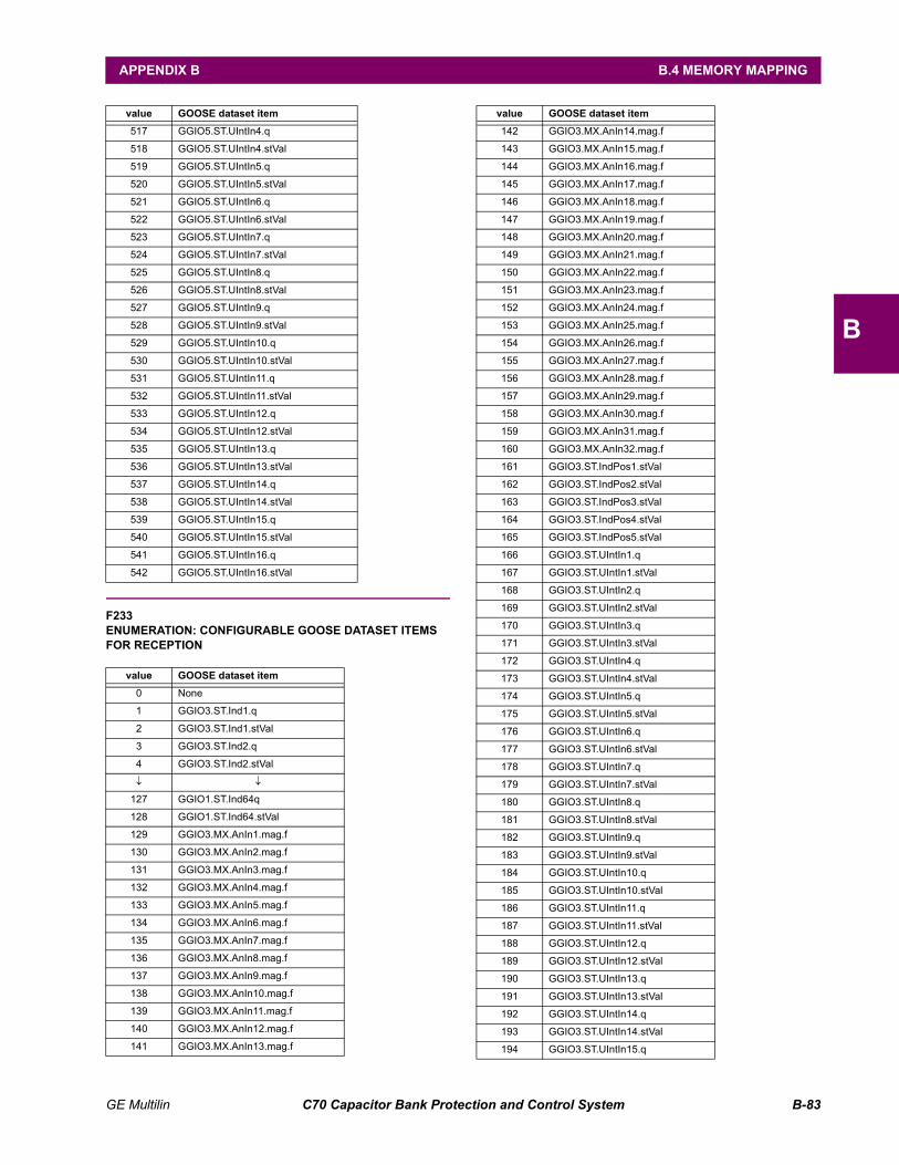
GE Multilin C70 Capacitor Bank Protection and Control System B-83
APPENDIX B B.4 MEMORY MAPPING
B
F233ENUMERATION: CONFIGURABLE GOOSE DATASET ITEMSFOR RECEPTION
517 GGIO5.ST.UIntIn4.q
518 GGIO5.ST.UIntIn4.stVal
519 GGIO5.ST.UIntIn5.q
520 GGIO5.ST.UIntIn5.stVal
521 GGIO5.ST.UIntIn6.q
522 GGIO5.ST.UIntIn6.stVal
523 GGIO5.ST.UIntIn7.q
524 GGIO5.ST.UIntIn7.stVal
525 GGIO5.ST.UIntIn8.q
526 GGIO5.ST.UIntIn8.stVal
527 GGIO5.ST.UIntIn9.q
528 GGIO5.ST.UIntIn9.stVal
529 GGIO5.ST.UIntIn10.q
530 GGIO5.ST.UIntIn10.stVal
531 GGIO5.ST.UIntIn11.q
532 GGIO5.ST.UIntIn11.stVal
533 GGIO5.ST.UIntIn12.q
534 GGIO5.ST.UIntIn12.stVal
535 GGIO5.ST.UIntIn13.q
536 GGIO5.ST.UIntIn13.stVal
537 GGIO5.ST.UIntIn14.q
538 GGIO5.ST.UIntIn14.stVal
539 GGIO5.ST.UIntIn15.q
540 GGIO5.ST.UIntIn15.stVal
541 GGIO5.ST.UIntIn16.q
542 GGIO5.ST.UIntIn16.stVal
value GOOSE dataset item
0 None
1 GGIO3.ST.Ind1.q
2 GGIO3.ST.Ind1.stVal
3 GGIO3.ST.Ind2.q
4 GGIO3.ST.Ind2.stVal
127 GGIO1.ST.Ind64q
128 GGIO1.ST.Ind64.stVal
129 GGIO3.MX.AnIn1.mag.f
130 GGIO3.MX.AnIn2.mag.f
131 GGIO3.MX.AnIn3.mag.f
132 GGIO3.MX.AnIn4.mag.f
133 GGIO3.MX.AnIn5.mag.f
134 GGIO3.MX.AnIn6.mag.f
135 GGIO3.MX.AnIn7.mag.f
136 GGIO3.MX.AnIn8.mag.f
137 GGIO3.MX.AnIn9.mag.f
138 GGIO3.MX.AnIn10.mag.f
139 GGIO3.MX.AnIn11.mag.f
140 GGIO3.MX.AnIn12.mag.f
141 GGIO3.MX.AnIn13.mag.f
value GOOSE dataset item
142 GGIO3.MX.AnIn14.mag.f
143 GGIO3.MX.AnIn15.mag.f
144 GGIO3.MX.AnIn16.mag.f
145 GGIO3.MX.AnIn17.mag.f
146 GGIO3.MX.AnIn18.mag.f
147 GGIO3.MX.AnIn19.mag.f
148 GGIO3.MX.AnIn20.mag.f
149 GGIO3.MX.AnIn21.mag.f
150 GGIO3.MX.AnIn22.mag.f
151 GGIO3.MX.AnIn23.mag.f
152 GGIO3.MX.AnIn24.mag.f
153 GGIO3.MX.AnIn25.mag.f
154 GGIO3.MX.AnIn26.mag.f
155 GGIO3.MX.AnIn27.mag.f
156 GGIO3.MX.AnIn28.mag.f
157 GGIO3.MX.AnIn29.mag.f
158 GGIO3.MX.AnIn30.mag.f
159 GGIO3.MX.AnIn31.mag.f
160 GGIO3.MX.AnIn32.mag.f
161 GGIO3.ST.IndPos1.stVal
162 GGIO3.ST.IndPos2.stVal
163 GGIO3.ST.IndPos3.stVal
164 GGIO3.ST.IndPos4.stVal
165 GGIO3.ST.IndPos5.stVal
166 GGIO3.ST.UIntIn1.q
167 GGIO3.ST.UIntIn1.stVal
168 GGIO3.ST.UIntIn2.q
169 GGIO3.ST.UIntIn2.stVal
170 GGIO3.ST.UIntIn3.q
171 GGIO3.ST.UIntIn3.stVal
172 GGIO3.ST.UIntIn4.q
173 GGIO3.ST.UIntIn4.stVal
174 GGIO3.ST.UIntIn5.q
175 GGIO3.ST.UIntIn5.stVal
176 GGIO3.ST.UIntIn6.q
177 GGIO3.ST.UIntIn6.stVal
178 GGIO3.ST.UIntIn7.q
179 GGIO3.ST.UIntIn7.stVal
180 GGIO3.ST.UIntIn8.q
181 GGIO3.ST.UIntIn8.stVal
182 GGIO3.ST.UIntIn9.q
183 GGIO3.ST.UIntIn9.stVal
184 GGIO3.ST.UIntIn10.q
185 GGIO3.ST.UIntIn10.stVal
186 GGIO3.ST.UIntIn11.q
187 GGIO3.ST.UIntIn11.stVal
188 GGIO3.ST.UIntIn12.q
189 GGIO3.ST.UIntIn12.stVal
190 GGIO3.ST.UIntIn13.q
191 GGIO3.ST.UIntIn13.stVal
192 GGIO3.ST.UIntIn14.q
193 GGIO3.ST.UIntIn14.stVal
194 GGIO3.ST.UIntIn15.q
value GOOSE dataset item

B-84 C70 Capacitor Bank Protection and Control System GE Multilin
B.4 MEMORY MAPPING APPENDIX B
B
F236ENUMERATION: WATTMETRIC GRN FLT CURVE
0 = Definite Time, 1 = Inverse, 2 = FlexCurve A, 3 = FlexCurve B,4 = FlexCurve C, 5 = FlexCurve D
F237ENUMERATION: REAL TIME CLOCK MONTH
F238ENUMERATION: REAL TIME CLOCK DAY
F239ENUMERATION: REAL TIME CLOCK DAYLIGHT SAVINGSTIME START DAY INSTANCE
F241ENUMERATION: NEUTRAL VOLTAGE UNBALANCE BUS 3V0
0 = Calculated, 1 = Measured
F243ENUMERATION: FIELD UNIT TYPE
0 = CC-05, 1 = CV-05, 2 = CC-01, 3 = CV-01
F244ENUMERATION: PROCESS CARD PORT
0 = H4a, 1 = H4b 2 = H3a, 3 = H3b, 4 = H2a, 5 = H2b, 6 = H1a, 7 = H1b
F245ENUMERATION: TEST MODE FUNCTION
F255ENUMERATION: CAPACITOR BANK GROUNDING
F257ENUMERATION: PROCESS CARD DSP CONFIGURATION
F260ENUMERATION: DATA LOGGER MODE
0 = Continuous, 1 = Trigger
F261ENUMERATION: BANK REDUNDANCY TYPE
0 = None, 1 = Dependability Biased, 2 = Security Biased
F263ENUMERATION: PROCESS BUS SYSTEM STATUS
0 = N/A, 1 = OK, 2 = Fail
195 GGIO3.ST.UIntIn15.stVal
196 GGIO3.ST.UIntIn16.q
197 GGIO3.ST.UIntIn16.stVal
value month
0 January
1 February
2 March
3 April
4 May
5 June
6 July
7 August
8 September
9 October
10 November
11 December
value day
0 Sunday
1 Monday
2 Tuesday
3 Wednesday
4 Thursday
5 Friday
6 Saturday
value instance
0 First
1 Second
2 Third
3 Fourth
4 Last
value GOOSE dataset item
Value Function
0 Disabled
1 Isolated
2 Forcible
Value Description
0 VT (ungrounded)
1 CTxR (grounded
value instance
0 CC
1 CV
2 CD
3 VC
4 VV
5 VD
6 DC
7 DV
8 DD

GE Multilin C70 Capacitor Bank Protection and Control System B-85
APPENDIX B B.4 MEMORY MAPPING
B
F300UR_UINT16: FLEXLOGIC BASE TYPE (6-bit type)
The FlexLogic BASE type is 7 bits and is combined with an 8-bitdescriptor and 1 bit for protection element to form a 16-bit value.The combined bits are of the form: PTTTTTTTDDDDDDDD,where P bit if set, indicates that the FlexLogic type is associatedwith a protection element state and T represents bits for the BASEtype, and D represents bits for the descriptor.
The values in square brackets indicate the base type with P prefix[PTTTTTTT] and the values in round brackets indicate the descrip-tor range. The right most T bit indicates whether the type is an ONor OFF type. There can be a total of 64 types (plus protection ele-ments). There can be a total of 256 descriptors of each type.
[0] Off (0) – this is boolean FALSE value[1] On (1) – this is boolean TRUE value[2] CONTACT INPUTS (1 to 96)[3] CONTACT INPUTS OFF (1 to 96)[4] VIRTUAL INPUTS (1 to 32)[6] VIRTUAL OUTPUTS (1 to 64[8] CONTACT OUTPUTS10] CONTACT OUTPUTS VOLTAGE DETECTED (1 to 64) [11] CONTACT OUTPUTS VOLTAGE OFF DETECTED (1 to 64)[12] CONTACT OUTPUTS CURRENT DETECTED (1 to 64)[13] CONTACT OUTPUTS CURRENT OFF DETECTED (1 to 64)[14] REMOTE INPUTS (1 to 32)[16] DIRECT INPUTS (1 to 96)[18] REMOTE OUTPUT DNA BIT PAIRS (1 to 32)[20] REMOTE OUTPUT UserSt BIT PAIRS (1 to 32)[22] REMOTE DEVICE ONLINE (1 to 16)[24] MISCELLANEOUS EQUATION[26] TELEPROTECTION INPUTS[28] INSERT (via keypad only)[30] DELETE (via keypad only)[32] END[34] NOT (1 INPUT)[36] 2 INPUT XOR (0)[38] LATCH SET/RESET (2 inputs)[40] OR (2 to 16 inputs)[42] AND (2 to 16 inputs)[44] NOR (2 to 16 inputs)[[46] NAND (2 to 16 inputs)[48] TIMER (1 to 32)[50] ASSIGN VIRTUAL OUTPUT (1 to 64)[52] ONE SHOT[54] SELF-TEST ERROR (see F141 for range)[56] PLATFORM DIRECT INPUT (1 to 96)[58] PLATFORM DIRECT OUTPUT (1 to 96)[60] PLATFORM DIRECT DEVICE (1 to 8)[62] MISCELLANEOUS EVENTS (see F146 for range)[64] PDC NETWORK CONTROL[66] PMU RECORDERE OUT OF MEMORY
[68] PMU RECORDER STOPPED[128 to 255] ELEMENT STATES (see memory map element statessection)
F400UR_UINT16: CT/VT BANK SELECTION
F491ENUMERATION: ANALOG INPUT MODE
0 = Default Value, 1 = Last Known
F500UR_UINT16: PACKED BITFIELD
First register indicates input/output state with bits 0 (MSB) to 15(LSB) corresponding to input/output state 1 to 16. The second reg-ister indicates input/output state with bits 0 to 15 corresponding toinput/output state 17 to 32 (if required) The third register indicatesinput/output state with bits 0 to 15 corresponding to input/outputstate 33 to 48 (if required). The fourth register indicates input/out-put state with bits 0 to 15 corresponding to input/output state 49 to64 (if required).
The number of registers required is determined by the specificdata item. A bit value of 0 = Off and 1 = On.
F501UR_UINT16: LED STATUS
Low byte of register indicates LED status with bit 0 representingthe top LED and bit 7 the bottom LED. A bit value of 1 indicatesthe LED is on, 0 indicates the LED is off.
F502BITFIELD: ELEMENT OPERATE STATES
Each bit contains the operate state for an element. See the F124format code for a list of element IDs. The operate bit for element IDX is bit [X mod 16] in register [X/16].
bitmask bank selection
0 Card 1 Contact 1 to 4
1 Card 1 Contact 5 to 8
2 Card 2 Contact 1 to 4
3 Card 2 Contact 5 to 8
4 Card 3 Contact 1 to 4
5 Card 3 Contact 5 to 8

B-86 C70 Capacitor Bank Protection and Control System GE Multilin
B.4 MEMORY MAPPING APPENDIX B
B
F504BITFIELD: 3-PHASE ELEMENT STATE
F505BITFIELD: CONTACT OUTPUT STATE
0 = Contact State, 1 = Voltage Detected, 2 = Current Detected
F507BITFIELD: COUNTER ELEMENT STATE
0 = Count Greater Than, 1 = Count Equal To, 2 = Count Less Than
F509BITFIELD: SIMPLE ELEMENT STATE
0 = Operate
F511BITFIELD: 3-PHASE SIMPLE ELEMENT STATE
0 = Operate, 1 = Operate A, 2 = Operate B, 3 = Operate C
F512ENUMERATION: HARMONIC NUMBER
F515ENUMERATION ELEMENT INPUT MODE
0 = Signed, 1 = Absolute
F516ENUMERATION ELEMENT COMPARE MODE
0 = Level, 1 = Delta
F518ENUMERATION: FLEXELEMENT UNITS
0 = Milliseconds, 1 = Seconds, 2 = Minutes
F519ENUMERATION: NON-VOLATILE LATCH
0 = Reset-Dominant, 1 = Set-Dominant
F522ENUMERATION: TRANSDUCER DCMA OUTPUT RANGE
0 = –1 to 1 mA; 1 = 0 to 1 mA; 2 = 4 to 20 mA
F523ENUMERATION: DNP OBJECTS 20, 22, AND 23 DEFAULTVARIATION
F524ENUMERATION: DNP OBJECT 21 DEFAULT VARIATION
F525ENUMERATION: DNP OBJECT 32 DEFAULT VARIATION
bitmask element state
0 Pickup
1 Operate
2 Pickup Phase A
3 Pickup Phase B
4 Pickup Phase C
5 Operate Phase A
6 Operate Phase B
7 Operate Phase C
bitmask harmonic bitmask harmonic
0 2ND 12 14TH
1 3RD 13 15TH
2 4TH 14 16TH
3 5TH 15 17TH
4 6TH 16 18TH
5 7TH 17 19TH
6 8TH 18 20TH
7 9TH 19 21ST
8 10TH 20 22ND
9 11TH 21 23RD
10 12TH 22 24TH
11 13TH 23 25TH
bitmask default variation
0 1
1 2
2 5
3 6
bitmask Default Variation
0 1
1 2
2 9
3 10
bitmask default variation
0 1
1 2
2 3
3 4
4 5
5 7

GE Multilin C70 Capacitor Bank Protection and Control System B-87
APPENDIX B B.4 MEMORY MAPPING
B
F530ENUMERATION: FRONT PANEL INTERFACE KEYPRESS
F531ENUMERATION: LANGUAGE
0 = English, 1 = French, 2 = Chinese, 3 = Russian, 4 = Turkish
F535ENUMERATION: AUTOMATIC VOLTAGE REGULATOROPERATING SIGNAL
0 = Vab, 1 = Vbc, 2 = Vca, 3 = Vavg, 4 = V1, 5 = Vaux
F536ENUMERATION: AUTOMATIC VOLTAGE REGULATORCONTROL MODE
0 = Voltage, 1 = Var
F537ENUMERATION: AUTOMATIC VOLTAGE REGULATOR VAROPEN MODE
0 = Minimize uptime, 1 = Minimize number of operations
F600UR_UINT16: FLEXANALOG PARAMETER
Corresponds to the Modbus address of the value used when thisparameter is selected. Only certain values may be used as Flex-Analogs (basically all metering quantities used in protection).
F605ENUMERATION: REMOTE DOUBLE-POINT STATUS INPUTSTATUS
F606ENUMERATION: REMOTE DOUBLE-POINT STATUS INPUT
F611ENUMERATION: GOOSE RETRANSMISSION SCHEME
F612UR_UINT16: FLEXINTEGER PARAMETER
This 16-bit value corresponds to the Modbus address of theselected FlexInteger parameter. Only certain values may be usedas FlexIntegers.
F615ENUMERATION: IEC 61850 REPORT DATASET ITEMS
value keypress value keypress value keypress
0 None 15 3 33 User PB 3
1 Menu 16 Enter 34 User PB 4
2 Message Up 17 Message Down
35 User PB 5
3 7 ~ 18 0 ~ 36 User PB 6
4 8 19 Decimal 37 User PB 7
5 9 20 +/– 38 User PB 8
6 Help 21 Value Up 39 User PB 9
7 Message Left 22 Value Down 40 User PB 10
8 4 23 Reset 41 User PB 11
9 5 24 User 1 42 User PB 12
10 6 25 User 2 44 User 4
11 Escape 26 User 3 45 User 5
12 Message Right
31 User PB 1 46 User 6
13 1 32 User PB 2 47 User 7
14 2
Enumeration Remote DPS input status
0 Intermediate
1 Off
2 On
3 Bad
Enumeration Remote double-point status input
0 None
1 Remote input 1
2 Remote input 2
3 Remote input 3
64 Remote input 64
Enumeration Configurable GOOSE retransmission scheme
0 Heartbeat
1 Aggressive
2 Medium
3 Relaxed
Enumeration IEC 61850 report dataset items
0 None
1 PDIF1.ST.Str.general
2 PDIF1.ST.Op.general
3 PDIF2.ST.Str.general
4 PDIF2.ST.Op.general
5 PDIF3.ST.Str.general
6 PDIF3.ST.Op.general
7 PDIF4.ST.Str.general
8 PDIF4.ST.Op.general
9 PDIS1.ST.Str.general
10 PDIS1.ST.Op.general
11 PDIS2.ST.Str.general
12 PDIS2.ST.Op.general
13 PDIS3.ST.Str.general

B-88 C70 Capacitor Bank Protection and Control System GE Multilin
B.4 MEMORY MAPPING APPENDIX B
B
14 PDIS3.ST.Op.general
15 PDIS4.ST.Str.general
16 PDIS4.ST.Op.general
17 PDIS5.ST.Str.general
18 PDIS5.ST.Op.general
19 PDIS6.ST.Str.general
20 PDIS6.ST.Op.general
21 PDIS7.ST.Str.general
22 PDIS7.ST.Op.general
23 PDIS8.ST.Str.general
24 PDIS8.ST.Op.general
25 PDIS9.ST.Str.general
26 PDIS9.ST.Op.general
27 PDIS10.ST.Str.general
28 PDIS10.ST.Op.general
29 PIOC1.ST.Str.general
30 PIOC1.ST.Op.general
31 PIOC2.ST.Str.general
32 PIOC2.ST.Op.general
33 PIOC3.ST.Str.general
34 PIOC3.ST.Op.general
35 PIOC4.ST.Str.general
36 PIOC4.ST.Op.general
37 PIOC5.ST.Str.general
38 PIOC5.ST.Op.general
39 PIOC6.ST.Str.general
40 PIOC6.ST.Op.general
41 PIOC7.ST.Str.general
42 PIOC7.ST.Op.general
43 PIOC8.ST.Str.general
44 PIOC8.ST.Op.general
45 PIOC9.ST.Str.general
46 PIOC9.ST.Op.general
47 PIOC10.ST.Str.general
48 PIOC10.ST.Op.general
49 PIOC11.ST.Str.general
50 PIOC11.ST.Op.general
51 PIOC12.ST.Str.general
52 PIOC12.ST.Op.general
53 PIOC13.ST.Str.general
54 PIOC13.ST.Op.general
55 PIOC14.ST.Str.general
56 PIOC14.ST.Op.general
57 PIOC15.ST.Str.general
58 PIOC15.ST.Op.general
59 PIOC16.ST.Str.general
60 PIOC16.ST.Op.general
61 PIOC17.ST.Str.general
62 PIOC17.ST.Op.general
63 PIOC18.ST.Str.general
64 PIOC18.ST.Op.general
65 PIOC19.ST.Str.general
66 PIOC19.ST.Op.general
Enumeration IEC 61850 report dataset items
67 PIOC20.ST.Str.general
68 PIOC20.ST.Op.general
69 PIOC21.ST.Str.general
70 PIOC21.ST.Op.general
71 PIOC22.ST.Str.general
72 PIOC22.ST.Op.general
73 PIOC23.ST.Str.general
74 PIOC23.ST.Op.general
75 PIOC24.ST.Str.general
76 PIOC24.ST.Op.general
77 PIOC25.ST.Str.general
78 PIOC25.ST.Op.general
79 PIOC26.ST.Str.general
80 PIOC26.ST.Op.general
81 PIOC27.ST.Str.general
82 PIOC27.ST.Op.general
83 PIOC28.ST.Str.general
84 PIOC28.ST.Op.general
85 PIOC29.ST.Str.general
86 PIOC29.ST.Op.general
87 PIOC30.ST.Str.general
88 PIOC30.ST.Op.general
89 PIOC31.ST.Str.general
90 PIOC31.ST.Op.general
91 PIOC32.ST.Str.general
92 PIOC32.ST.Op.general
93 PIOC33.ST.Str.general
94 PIOC33.ST.Op.general
95 PIOC34.ST.Str.general
96 PIOC34.ST.Op.general
97 PIOC35.ST.Str.general
98 PIOC35.ST.Op.general
99 PIOC36.ST.Str.general
100 PIOC36.ST.Op.general
101 PIOC37.ST.Str.general
102 PIOC37.ST.Op.general
103 PIOC38.ST.Str.general
104 PIOC38.ST.Op.general
105 PIOC39.ST.Str.general
106 PIOC39.ST.Op.general
107 PIOC40.ST.Str.general
108 PIOC40.ST.Op.general
109 PIOC41.ST.Str.general
110 PIOC41.ST.Op.general
111 PIOC42.ST.Str.general
112 PIOC42.ST.Op.general
113 PIOC43.ST.Str.general
114 PIOC43.ST.Op.general
115 PIOC44.ST.Str.general
116 PIOC44.ST.Op.general
117 PIOC45.ST.Str.general
118 PIOC45.ST.Op.general
119 PIOC46.ST.Str.general
Enumeration IEC 61850 report dataset items
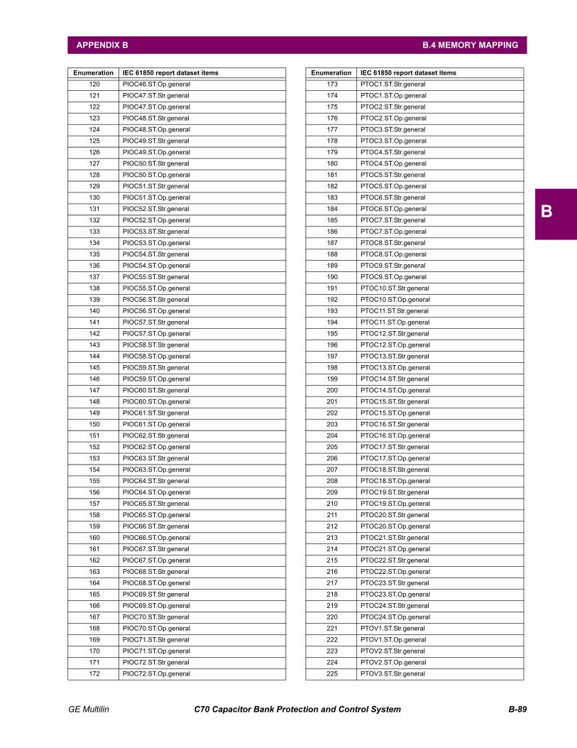
GE Multilin C70 Capacitor Bank Protection and Control System B-89
APPENDIX B B.4 MEMORY MAPPING
B
120 PIOC46.ST.Op.general
121 PIOC47.ST.Str.general
122 PIOC47.ST.Op.general
123 PIOC48.ST.Str.general
124 PIOC48.ST.Op.general
125 PIOC49.ST.Str.general
126 PIOC49.ST.Op.general
127 PIOC50.ST.Str.general
128 PIOC50.ST.Op.general
129 PIOC51.ST.Str.general
130 PIOC51.ST.Op.general
131 PIOC52.ST.Str.general
132 PIOC52.ST.Op.general
133 PIOC53.ST.Str.general
134 PIOC53.ST.Op.general
135 PIOC54.ST.Str.general
136 PIOC54.ST.Op.general
137 PIOC55.ST.Str.general
138 PIOC55.ST.Op.general
139 PIOC56.ST.Str.general
140 PIOC56.ST.Op.general
141 PIOC57.ST.Str.general
142 PIOC57.ST.Op.general
143 PIOC58.ST.Str.general
144 PIOC58.ST.Op.general
145 PIOC59.ST.Str.general
146 PIOC59.ST.Op.general
147 PIOC60.ST.Str.general
148 PIOC60.ST.Op.general
149 PIOC61.ST.Str.general
150 PIOC61.ST.Op.general
151 PIOC62.ST.Str.general
152 PIOC62.ST.Op.general
153 PIOC63.ST.Str.general
154 PIOC63.ST.Op.general
155 PIOC64.ST.Str.general
156 PIOC64.ST.Op.general
157 PIOC65.ST.Str.general
158 PIOC65.ST.Op.general
159 PIOC66.ST.Str.general
160 PIOC66.ST.Op.general
161 PIOC67.ST.Str.general
162 PIOC67.ST.Op.general
163 PIOC68.ST.Str.general
164 PIOC68.ST.Op.general
165 PIOC69.ST.Str.general
166 PIOC69.ST.Op.general
167 PIOC70.ST.Str.general
168 PIOC70.ST.Op.general
169 PIOC71.ST.Str.general
170 PIOC71.ST.Op.general
171 PIOC72.ST.Str.general
172 PIOC72.ST.Op.general
Enumeration IEC 61850 report dataset items
173 PTOC1.ST.Str.general
174 PTOC1.ST.Op.general
175 PTOC2.ST.Str.general
176 PTOC2.ST.Op.general
177 PTOC3.ST.Str.general
178 PTOC3.ST.Op.general
179 PTOC4.ST.Str.general
180 PTOC4.ST.Op.general
181 PTOC5.ST.Str.general
182 PTOC5.ST.Op.general
183 PTOC6.ST.Str.general
184 PTOC6.ST.Op.general
185 PTOC7.ST.Str.general
186 PTOC7.ST.Op.general
187 PTOC8.ST.Str.general
188 PTOC8.ST.Op.general
189 PTOC9.ST.Str.general
190 PTOC9.ST.Op.general
191 PTOC10.ST.Str.general
192 PTOC10.ST.Op.general
193 PTOC11.ST.Str.general
194 PTOC11.ST.Op.general
195 PTOC12.ST.Str.general
196 PTOC12.ST.Op.general
197 PTOC13.ST.Str.general
198 PTOC13.ST.Op.general
199 PTOC14.ST.Str.general
200 PTOC14.ST.Op.general
201 PTOC15.ST.Str.general
202 PTOC15.ST.Op.general
203 PTOC16.ST.Str.general
204 PTOC16.ST.Op.general
205 PTOC17.ST.Str.general
206 PTOC17.ST.Op.general
207 PTOC18.ST.Str.general
208 PTOC18.ST.Op.general
209 PTOC19.ST.Str.general
210 PTOC19.ST.Op.general
211 PTOC20.ST.Str.general
212 PTOC20.ST.Op.general
213 PTOC21.ST.Str.general
214 PTOC21.ST.Op.general
215 PTOC22.ST.Str.general
216 PTOC22.ST.Op.general
217 PTOC23.ST.Str.general
218 PTOC23.ST.Op.general
219 PTOC24.ST.Str.general
220 PTOC24.ST.Op.general
221 PTOV1.ST.Str.general
222 PTOV1.ST.Op.general
223 PTOV2.ST.Str.general
224 PTOV2.ST.Op.general
225 PTOV3.ST.Str.general
Enumeration IEC 61850 report dataset items
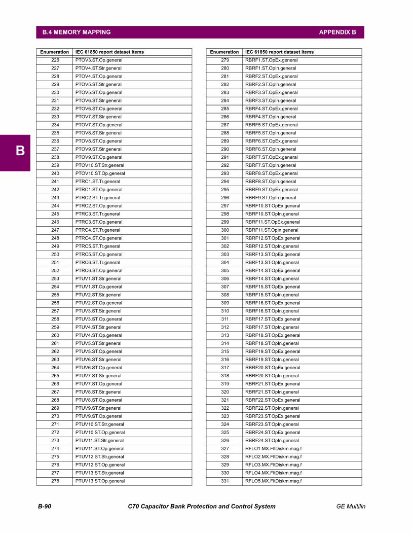
B-90 C70 Capacitor Bank Protection and Control System GE Multilin
B.4 MEMORY MAPPING APPENDIX B
B
226 PTOV3.ST.Op.general
227 PTOV4.ST.Str.general
228 PTOV4.ST.Op.general
229 PTOV5.ST.Str.general
230 PTOV5.ST.Op.general
231 PTOV6.ST.Str.general
232 PTOV6.ST.Op.general
233 PTOV7.ST.Str.general
234 PTOV7.ST.Op.general
235 PTOV8.ST.Str.general
236 PTOV8.ST.Op.general
237 PTOV9.ST.Str.general
238 PTOV9.ST.Op.general
239 PTOV10.ST.Str.general
240 PTOV10.ST.Op.general
241 PTRC1.ST.Tr.general
242 PTRC1.ST.Op.general
243 PTRC2.ST.Tr.general
244 PTRC2.ST.Op.general
245 PTRC3.ST.Tr.general
246 PTRC3.ST.Op.general
247 PTRC4.ST.Tr.general
248 PTRC4.ST.Op.general
249 PTRC5.ST.Tr.general
250 PTRC5.ST.Op.general
251 PTRC6.ST.Tr.general
252 PTRC6.ST.Op.general
253 PTUV1.ST.Str.general
254 PTUV1.ST.Op.general
255 PTUV2.ST.Str.general
256 PTUV2.ST.Op.general
257 PTUV3.ST.Str.general
258 PTUV3.ST.Op.general
259 PTUV4.ST.Str.general
260 PTUV4.ST.Op.general
261 PTUV5.ST.Str.general
262 PTUV5.ST.Op.general
263 PTUV6.ST.Str.general
264 PTUV6.ST.Op.general
265 PTUV7.ST.Str.general
266 PTUV7.ST.Op.general
267 PTUV8.ST.Str.general
268 PTUV8.ST.Op.general
269 PTUV9.ST.Str.general
270 PTUV9.ST.Op.general
271 PTUV10.ST.Str.general
272 PTUV10.ST.Op.general
273 PTUV11.ST.Str.general
274 PTUV11.ST.Op.general
275 PTUV12.ST.Str.general
276 PTUV12.ST.Op.general
277 PTUV13.ST.Str.general
278 PTUV13.ST.Op.general
Enumeration IEC 61850 report dataset items
279 RBRF1.ST.OpEx.general
280 RBRF1.ST.OpIn.general
281 RBRF2.ST.OpEx.general
282 RBRF2.ST.OpIn.general
283 RBRF3.ST.OpEx.general
284 RBRF3.ST.OpIn.general
285 RBRF4.ST.OpEx.general
286 RBRF4.ST.OpIn.general
287 RBRF5.ST.OpEx.general
288 RBRF5.ST.OpIn.general
289 RBRF6.ST.OpEx.general
290 RBRF6.ST.OpIn.general
291 RBRF7.ST.OpEx.general
292 RBRF7.ST.OpIn.general
293 RBRF8.ST.OpEx.general
294 RBRF8.ST.OpIn.general
295 RBRF9.ST.OpEx.general
296 RBRF9.ST.OpIn.general
297 RBRF10.ST.OpEx.general
298 RBRF10.ST.OpIn.general
299 RBRF11.ST.OpEx.general
300 RBRF11.ST.OpIn.general
301 RBRF12.ST.OpEx.general
302 RBRF12.ST.OpIn.general
303 RBRF13.ST.OpEx.general
304 RBRF13.ST.OpIn.general
305 RBRF14.ST.OpEx.general
306 RBRF14.ST.OpIn.general
307 RBRF15.ST.OpEx.general
308 RBRF15.ST.OpIn.general
309 RBRF16.ST.OpEx.general
310 RBRF16.ST.OpIn.general
311 RBRF17.ST.OpEx.general
312 RBRF17.ST.OpIn.general
313 RBRF18.ST.OpEx.general
314 RBRF18.ST.OpIn.general
315 RBRF19.ST.OpEx.general
316 RBRF19.ST.OpIn.general
317 RBRF20.ST.OpEx.general
318 RBRF20.ST.OpIn.general
319 RBRF21.ST.OpEx.general
320 RBRF21.ST.OpIn.general
321 RBRF22.ST.OpEx.general
322 RBRF22.ST.OpIn.general
323 RBRF23.ST.OpEx.general
324 RBRF23.ST.OpIn.general
325 RBRF24.ST.OpEx.general
326 RBRF24.ST.OpIn.general
327 RFLO1.MX.FltDiskm.mag.f
328 RFLO2.MX.FltDiskm.mag.f
329 RFLO3.MX.FltDiskm.mag.f
330 RFLO4.MX.FltDiskm.mag.f
331 RFLO5.MX.FltDiskm.mag.f
Enumeration IEC 61850 report dataset items

GE Multilin C70 Capacitor Bank Protection and Control System B-91
APPENDIX B B.4 MEMORY MAPPING
B
332 RPSB1.ST.Str.general
333 RPSB1.ST.Op.general
334 RPSB1.ST.BlkZn.stVal
335 RREC1.ST.Op.general
336 RREC1.ST.AutoRecSt.stVal
337 RREC2.ST.Op.general
338 RREC2.ST.AutoRecSt.stVal
339 RREC3.ST.Op.general
340 RREC3.ST.AutoRecSt.stVal
341 RREC4.ST.Op.general
342 RREC4.ST.AutoRecSt.stVal
343 RREC5.ST.Op.general
344 RREC5.ST.AutoRecSt.stVal
345 RREC6.ST.Op.general
346 RREC6.ST.AutoRecSt.stVal
347 CSWI1.ST.Loc.stVal
348 CSWI1.ST.Pos.stVal
349 CSWI2.ST.Loc.stVal
350 CSWI2.ST.Pos.stVal
351 CSWI3.ST.Loc.stVal
352 CSWI3.ST.Pos.stVal
353 CSWI4.ST.Loc.stVal
354 CSWI4.ST.Pos.stVal
355 CSWI5.ST.Loc.stVal
356 CSWI5.ST.Pos.stVal
357 CSWI6.ST.Loc.stVal
358 CSWI6.ST.Pos.stVal
359 CSWI7.ST.Loc.stVal
360 CSWI7.ST.Pos.stVal
361 CSWI8.ST.Loc.stVal
362 CSWI8.ST.Pos.stVal
363 CSWI9.ST.Loc.stVal
364 CSWI9.ST.Pos.stVal
365 CSWI10.ST.Loc.stVal
366 CSWI10.ST.Pos.stVal
367 CSWI11.ST.Loc.stVal
368 CSWI11.ST.Pos.stVal
369 CSWI12.ST.Loc.stVal
370 CSWI12.ST.Pos.stVal
371 CSWI13.ST.Loc.stVal
372 CSWI13.ST.Pos.stVal
373 CSWI14.ST.Loc.stVal
374 CSWI14.ST.Pos.stVal
375 CSWI15.ST.Loc.stVal
376 CSWI15.ST.Pos.stVal
377 CSWI16.ST.Loc.stVal
378 CSWI16.ST.Pos.stVal
379 CSWI17.ST.Loc.stVal
380 CSWI17.ST.Pos.stVal
381 CSWI18.ST.Loc.stVal
382 CSWI18.ST.Pos.stVal
383 CSWI19.ST.Loc.stVal
384 CSWI19.ST.Pos.stVal
Enumeration IEC 61850 report dataset items
385 CSWI20.ST.Loc.stVal
386 CSWI20.ST.Pos.stVal
387 CSWI21.ST.Loc.stVal
388 CSWI21.ST.Pos.stVal
389 CSWI22.ST.Loc.stVal
390 CSWI22.ST.Pos.stVal
391 CSWI23.ST.Loc.stVal
392 CSWI23.ST.Pos.stVal
393 CSWI24.ST.Loc.stVal
394 CSWI24.ST.Pos.stVal
395 CSWI25.ST.Loc.stVal
396 CSWI25.ST.Pos.stVal
397 CSWI26.ST.Loc.stVal
398 CSWI26.ST.Pos.stVal
399 CSWI27.ST.Loc.stVal
400 CSWI27.ST.Pos.stVal
401 CSWI28.ST.Loc.stVal
402 CSWI28.ST.Pos.stVal
403 CSWI29.ST.Loc.stVal
404 CSWI29.ST.Pos.stVal
405 CSWI30.ST.Loc.stVal
406 CSWI30.ST.Pos.stVal
407 GGIO1.ST.Ind1.stVal
408 GGIO1.ST.Ind2.stVal
409 GGIO1.ST.Ind3.stVal
410 GGIO1.ST.Ind4.stVal
411 GGIO1.ST.Ind5.stVal
412 GGIO1.ST.Ind6.stVal
413 GGIO1.ST.Ind7.stVal
414 GGIO1.ST.Ind8.stVal
415 GGIO1.ST.Ind9.stVal
416 GGIO1.ST.Ind10.stVal
417 GGIO1.ST.Ind11.stVal
418 GGIO1.ST.Ind12.stVal
419 GGIO1.ST.Ind13.stVal
420 GGIO1.ST.Ind14.stVal
421 GGIO1.ST.Ind15.stVal
422 GGIO1.ST.Ind16.stVal
423 GGIO1.ST.Ind17.stVal
424 GGIO1.ST.Ind18.stVal
425 GGIO1.ST.Ind19.stVal
426 GGIO1.ST.Ind20.stVal
427 GGIO1.ST.Ind21.stVal
428 GGIO1.ST.Ind22.stVal
429 GGIO1.ST.Ind23.stVal
430 GGIO1.ST.Ind24.stVal
431 GGIO1.ST.Ind25.stVal
432 GGIO1.ST.Ind26.stVal
433 GGIO1.ST.Ind27.stVal
434 GGIO1.ST.Ind28.stVal
435 GGIO1.ST.Ind29.stVal
436 GGIO1.ST.Ind30.stVal
437 GGIO1.ST.Ind31.stVal
Enumeration IEC 61850 report dataset items

B-92 C70 Capacitor Bank Protection and Control System GE Multilin
B.4 MEMORY MAPPING APPENDIX B
B
438 GGIO1.ST.Ind32.stVal
439 GGIO1.ST.Ind33.stVal
440 GGIO1.ST.Ind34.stVal
441 GGIO1.ST.Ind35.stVal
442 GGIO1.ST.Ind36.stVal
443 GGIO1.ST.Ind37.stVal
444 GGIO1.ST.Ind38.stVal
445 GGIO1.ST.Ind39.stVal
446 GGIO1.ST.Ind40.stVal
447 GGIO1.ST.Ind41.stVal
448 GGIO1.ST.Ind42.stVal
449 GGIO1.ST.Ind43.stVal
450 GGIO1.ST.Ind44.stVal
451 GGIO1.ST.Ind45.stVal
452 GGIO1.ST.Ind46.stVal
453 GGIO1.ST.Ind47.stVal
454 GGIO1.ST.Ind48.stVal
455 GGIO1.ST.Ind49.stVal
456 GGIO1.ST.Ind50.stVal
457 GGIO1.ST.Ind51.stVal
458 GGIO1.ST.Ind52.stVal
459 GGIO1.ST.Ind53.stVal
460 GGIO1.ST.Ind54.stVal
461 GGIO1.ST.Ind55.stVal
462 GGIO1.ST.Ind56.stVal
463 GGIO1.ST.Ind57.stVal
464 GGIO1.ST.Ind58.stVal
465 GGIO1.ST.Ind59.stVal
466 GGIO1.ST.Ind60.stVal
467 GGIO1.ST.Ind61.stVal
468 GGIO1.ST.Ind62.stVal
469 GGIO1.ST.Ind63.stVal
470 GGIO1.ST.Ind64.stVal
471 GGIO1.ST.Ind65.stVal
472 GGIO1.ST.Ind66.stVal
473 GGIO1.ST.Ind67.stVal
474 GGIO1.ST.Ind68.stVal
475 GGIO1.ST.Ind69.stVal
476 GGIO1.ST.Ind70.stVal
477 GGIO1.ST.Ind71.stVal
478 GGIO1.ST.Ind72.stVal
479 GGIO1.ST.Ind73.stVal
480 GGIO1.ST.Ind74.stVal
481 GGIO1.ST.Ind75.stVal
482 GGIO1.ST.Ind76.stVal
483 GGIO1.ST.Ind77.stVal
484 GGIO1.ST.Ind78.stVal
485 GGIO1.ST.Ind79.stVal
486 GGIO1.ST.Ind80.stVal
487 GGIO1.ST.Ind81.stVal
488 GGIO1.ST.Ind82.stVal
489 GGIO1.ST.Ind83.stVal
490 GGIO1.ST.Ind84.stVal
Enumeration IEC 61850 report dataset items
491 GGIO1.ST.Ind85.stVal
492 GGIO1.ST.Ind86.stVal
493 GGIO1.ST.Ind87.stVal
494 GGIO1.ST.Ind88.stVal
495 GGIO1.ST.Ind89.stVal
496 GGIO1.ST.Ind90.stVal
497 GGIO1.ST.Ind91.stVal
498 GGIO1.ST.Ind92.stVal
499 GGIO1.ST.Ind93.stVal
500 GGIO1.ST.Ind94.stVal
501 GGIO1.ST.Ind95.stVal
502 GGIO1.ST.Ind96.stVal
503 GGIO1.ST.Ind97.stVal
504 GGIO1.ST.Ind98.stVal
505 GGIO1.ST.Ind99.stVal
506 GGIO1.ST.Ind100.stVal
507 GGIO1.ST.Ind101.stVal
508 GGIO1.ST.Ind102.stVal
509 GGIO1.ST.Ind103.stVal
510 GGIO1.ST.Ind104.stVal
511 GGIO1.ST.Ind105.stVal
512 GGIO1.ST.Ind106.stVal
513 GGIO1.ST.Ind107.stVal
514 GGIO1.ST.Ind108.stVal
515 GGIO1.ST.Ind109.stVal
516 GGIO1.ST.Ind110.stVal
517 GGIO1.ST.Ind111.stVal
518 GGIO1.ST.Ind112.stVal
519 GGIO1.ST.Ind113.stVal
520 GGIO1.ST.Ind114.stVal
521 GGIO1.ST.Ind115.stVal
522 GGIO1.ST.Ind116.stVal
523 GGIO1.ST.Ind117.stVal
524 GGIO1.ST.Ind118.stVal
525 GGIO1.ST.Ind119.stVal
526 GGIO1.ST.Ind120.stVal
527 GGIO1.ST.Ind121.stVal
528 GGIO1.ST.Ind122.stVal
529 GGIO1.ST.Ind123.stVal
530 GGIO1.ST.Ind124.stVal
531 GGIO1.ST.Ind125.stVal
532 GGIO1.ST.Ind126.stVal
533 GGIO1.ST.Ind127.stVal
534 GGIO1.ST.Ind128.stVal
535 MMXU1.MX.TotW.mag.f
536 MMXU1.MX.TotVAr.mag.f
537 MMXU1.MX.TotVA.mag.f
538 MMXU1.MX.TotPF.mag.f
539 MMXU1.MX.Hz.mag.f
540 MMXU1.MX.PPV.phsAB.cVal.mag.f
541 MMXU1.MX.PPV.phsAB.cVal.ang.f
542 MMXU1.MX.PPV.phsBC.cVal.mag.f
543 MMXU1.MX.PPV.phsBC.cVal.ang.f
Enumeration IEC 61850 report dataset items
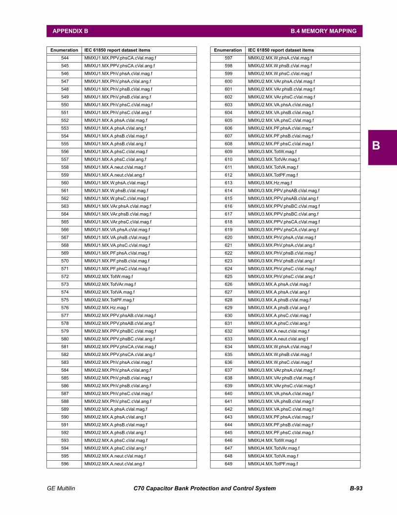
GE Multilin C70 Capacitor Bank Protection and Control System B-93
APPENDIX B B.4 MEMORY MAPPING
B
544 MMXU1.MX.PPV.phsCA.cVal.mag.f
545 MMXU1.MX.PPV.phsCA.cVal.ang.f
546 MMXU1.MX.PhV.phsA.cVal.mag.f
547 MMXU1.MX.PhV.phsA.cVal.ang.f
548 MMXU1.MX.PhV.phsB.cVal.mag.f
549 MMXU1.MX.PhV.phsB.cVal.ang.f
550 MMXU1.MX.PhV.phsC.cVal.mag.f
551 MMXU1.MX.PhV.phsC.cVal.ang.f
552 MMXU1.MX.A.phsA.cVal.mag.f
553 MMXU1.MX.A.phsA.cVal.ang.f
554 MMXU1.MX.A.phsB.cVal.mag.f
555 MMXU1.MX.A.phsB.cVal.ang.f
556 MMXU1.MX.A.phsC.cVal.mag.f
557 MMXU1.MX.A.phsC.cVal.ang.f
558 MMXU1.MX.A.neut.cVal.mag.f
559 MMXU1.MX.A.neut.cVal.ang.f
560 MMXU1.MX.W.phsA.cVal.mag.f
561 MMXU1.MX.W.phsB.cVal.mag.f
562 MMXU1.MX.W.phsC.cVal.mag.f
563 MMXU1.MX.VAr.phsA.cVal.mag.f
564 MMXU1.MX.VAr.phsB.cVal.mag.f
565 MMXU1.MX.VAr.phsC.cVal.mag.f
566 MMXU1.MX.VA.phsA.cVal.mag.f
567 MMXU1.MX.VA.phsB.cVal.mag.f
568 MMXU1.MX.VA.phsC.cVal.mag.f
569 MMXU1.MX.PF.phsA.cVal.mag.f
570 MMXU1.MX.PF.phsB.cVal.mag.f
571 MMXU1.MX.PF.phsC.cVal.mag.f
572 MMXU2.MX.TotW.mag.f
573 MMXU2.MX.TotVAr.mag.f
574 MMXU2.MX.TotVA.mag.f
575 MMXU2.MX.TotPF.mag.f
576 MMXU2.MX.Hz.mag.f
577 MMXU2.MX.PPV.phsAB.cVal.mag.f
578 MMXU2.MX.PPV.phsAB.cVal.ang.f
579 MMXU2.MX.PPV.phsBC.cVal.mag.f
580 MMXU2.MX.PPV.phsBC.cVal.ang.f
581 MMXU2.MX.PPV.phsCA.cVal.mag.f
582 MMXU2.MX.PPV.phsCA.cVal.ang.f
583 MMXU2.MX.PhV.phsA.cVal.mag.f
584 MMXU2.MX.PhV.phsA.cVal.ang.f
585 MMXU2.MX.PhV.phsB.cVal.mag.f
586 MMXU2.MX.PhV.phsB.cVal.ang.f
587 MMXU2.MX.PhV.phsC.cVal.mag.f
588 MMXU2.MX.PhV.phsC.cVal.ang.f
589 MMXU2.MX.A.phsA.cVal.mag.f
590 MMXU2.MX.A.phsA.cVal.ang.f
591 MMXU2.MX.A.phsB.cVal.mag.f
592 MMXU2.MX.A.phsB.cVal.ang.f
593 MMXU2.MX.A.phsC.cVal.mag.f
594 MMXU2.MX.A.phsC.cVal.ang.f
595 MMXU2.MX.A.neut.cVal.mag.f
596 MMXU2.MX.A.neut.cVal.ang.f
Enumeration IEC 61850 report dataset items
597 MMXU2.MX.W.phsA.cVal.mag.f
598 MMXU2.MX.W.phsB.cVal.mag.f
599 MMXU2.MX.W.phsC.cVal.mag.f
600 MMXU2.MX.VAr.phsA.cVal.mag.f
601 MMXU2.MX.VAr.phsB.cVal.mag.f
602 MMXU2.MX.VAr.phsC.cVal.mag.f
603 MMXU2.MX.VA.phsA.cVal.mag.f
604 MMXU2.MX.VA.phsB.cVal.mag.f
605 MMXU2.MX.VA.phsC.cVal.mag.f
606 MMXU2.MX.PF.phsA.cVal.mag.f
607 MMXU2.MX.PF.phsB.cVal.mag.f
608 MMXU2.MX.PF.phsC.cVal.mag.f
609 MMXU3.MX.TotW.mag.f
610 MMXU3.MX.TotVAr.mag.f
611 MMXU3.MX.TotVA.mag.f
612 MMXU3.MX.TotPF.mag.f
613 MMXU3.MX.Hz.mag.f
614 MMXU3.MX.PPV.phsAB.cVal.mag.f
615 MMXU3.MX.PPV.phsAB.cVal.ang.f
616 MMXU3.MX.PPV.phsBC.cVal.mag.f
617 MMXU3.MX.PPV.phsBC.cVal.ang.f
618 MMXU3.MX.PPV.phsCA.cVal.mag.f
619 MMXU3.MX.PPV.phsCA.cVal.ang.f
620 MMXU3.MX.PhV.phsA.cVal.mag.f
621 MMXU3.MX.PhV.phsA.cVal.ang.f
622 MMXU3.MX.PhV.phsB.cVal.mag.f
623 MMXU3.MX.PhV.phsB.cVal.ang.f
624 MMXU3.MX.PhV.phsC.cVal.mag.f
625 MMXU3.MX.PhV.phsC.cVal.ang.f
626 MMXU3.MX.A.phsA.cVal.mag.f
627 MMXU3.MX.A.phsA.cVal.ang.f
628 MMXU3.MX.A.phsB.cVal.mag.f
629 MMXU3.MX.A.phsB.cVal.ang.f
630 MMXU3.MX.A.phsC.cVal.mag.f
631 MMXU3.MX.A.phsC.cVal.ang.f
632 MMXU3.MX.A.neut.cVal.mag.f
633 MMXU3.MX.A.neut.cVal.ang.f
634 MMXU3.MX.W.phsA.cVal.mag.f
635 MMXU3.MX.W.phsB.cVal.mag.f
636 MMXU3.MX.W.phsC.cVal.mag.f
637 MMXU3.MX.VAr.phsA.cVal.mag.f
638 MMXU3.MX.VAr.phsB.cVal.mag.f
639 MMXU3.MX.VAr.phsC.cVal.mag.f
640 MMXU3.MX.VA.phsA.cVal.mag.f
641 MMXU3.MX.VA.phsB.cVal.mag.f
642 MMXU3.MX.VA.phsC.cVal.mag.f
643 MMXU3.MX.PF.phsA.cVal.mag.f
644 MMXU3.MX.PF.phsB.cVal.mag.f
645 MMXU3.MX.PF.phsC.cVal.mag.f
646 MMXU4.MX.TotW.mag.f
647 MMXU4.MX.TotVAr.mag.f
648 MMXU4.MX.TotVA.mag.f
649 MMXU4.MX.TotPF.mag.f
Enumeration IEC 61850 report dataset items
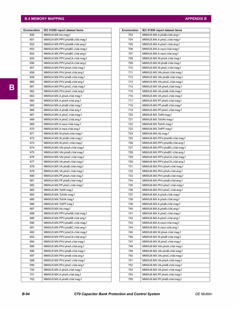
B-94 C70 Capacitor Bank Protection and Control System GE Multilin
B.4 MEMORY MAPPING APPENDIX B
B
650 MMXU4.MX.Hz.mag.f
651 MMXU4.MX.PPV.phsAB.cVal.mag.f
652 MMXU4.MX.PPV.phsAB.cVal.ang.f
653 MMXU4.MX.PPV.phsBC.cVal.mag.f
654 MMXU4.MX.PPV.phsBC.cVal.ang.f
655 MMXU4.MX.PPV.phsCA.cVal.mag.f
656 MMXU4.MX.PPV.phsCA.cVal.ang.f
657 MMXU4.MX.PhV.phsA.cVal.mag.f
658 MMXU4.MX.PhV.phsA.cVal.ang.f
659 MMXU4.MX.PhV.phsB.cVal.mag.f
660 MMXU4.MX.PhV.phsB.cVal.ang.f
661 MMXU4.MX.PhV.phsC.cVal.mag.f
662 MMXU4.MX.PhV.phsC.cVal.ang.f
663 MMXU4.MX.A.phsA.cVal.mag.f
664 MMXU4.MX.A.phsA.cVal.ang.f
665 MMXU4.MX.A.phsB.cVal.mag.f
666 MMXU4.MX.A.phsB.cVal.ang.f
667 MMXU4.MX.A.phsC.cVal.mag.f
668 MMXU4.MX.A.phsC.cVal.ang.f
669 MMXU4.MX.A.neut.cVal.mag.f
670 MMXU4.MX.A.neut.cVal.ang.f
671 MMXU4.MX.W.phsA.cVal.mag.f
672 MMXU4.MX.W.phsB.cVal.mag.f
673 MMXU4.MX.W.phsC.cVal.mag.f
674 MMXU4.MX.VAr.phsA.cVal.mag.f
675 MMXU4.MX.VAr.phsB.cVal.mag.f
676 MMXU4.MX.VAr.phsC.cVal.mag.f
677 MMXU4.MX.VA.phsA.cVal.mag.f
678 MMXU4.MX.VA.phsB.cVal.mag.f
679 MMXU4.MX.VA.phsC.cVal.mag.f
680 MMXU4.MX.PF.phsA.cVal.mag.f
681 MMXU4.MX.PF.phsB.cVal.mag.f
682 MMXU4.MX.PF.phsC.cVal.mag.f
683 MMXU5.MX.TotW.mag.f
684 MMXU5.MX.TotVAr.mag.f
685 MMXU5.MX.TotVA.mag.f
686 MMXU5.MX.TotPF.mag.f
687 MMXU5.MX.Hz.mag.f
688 MMXU5.MX.PPV.phsAB.cVal.mag.f
689 MMXU5.MX.PPV.phsAB.cVal.ang.f
690 MMXU5.MX.PPV.phsBC.cVal.mag.f
691 MMXU5.MX.PPV.phsBC.cVal.ang.f
692 MMXU5.MX.PPV.phsCA.cVal.mag.f
693 MMXU5.MX.PPV.phsCA.cVal.ang.f
694 MMXU5.MX.PhV.phsA.cVal.mag.f
695 MMXU5.MX.PhV.phsA.cVal.ang.f
696 MMXU5.MX.PhV.phsB.cVal.mag.f
697 MMXU5.MX.PhV.phsB.cVal.ang.f
698 MMXU5.MX.PhV.phsC.cVal.mag.f
699 MMXU5.MX.PhV.phsC.cVal.ang.f
700 MMXU5.MX.A.phsA.cVal.mag.f
701 MMXU5.MX.A.phsA.cVal.ang.f
702 MMXU5.MX.A.phsB.cVal.mag.f
Enumeration IEC 61850 report dataset items
703 MMXU5.MX.A.phsB.cVal.ang.f
704 MMXU5.MX.A.phsC.cVal.mag.f
705 MMXU5.MX.A.phsC.cVal.ang.f
706 MMXU5.MX.A.neut.cVal.mag.f
707 MMXU5.MX.A.neut.cVal.ang.f
708 MMXU5.MX.W.phsA.cVal.mag.f
709 MMXU5.MX.W.phsB.cVal.mag.f
710 MMXU5.MX.W.phsC.cVal.mag.f
711 MMXU5.MX.VAr.phsA.cVal.mag.f
712 MMXU5.MX.VAr.phsB.cVal.mag.f
713 MMXU5.MX.VAr.phsC.cVal.mag.f
714 MMXU5.MX.VA.phsA.cVal.mag.f
715 MMXU5.MX.VA.phsB.cVal.mag.f
716 MMXU5.MX.VA.phsC.cVal.mag.f
717 MMXU5.MX.PF.phsA.cVal.mag.f
718 MMXU5.MX.PF.phsB.cVal.mag.f
719 MMXU5.MX.PF.phsC.cVal.mag.f
720 MMXU6.MX.TotW.mag.f
721 MMXU6.MX.TotVAr.mag.f
722 MMXU6.MX.TotVA.mag.f
723 MMXU6.MX.TotPF.mag.f
724 MMXU6.MX.Hz.mag.f
725 MMXU6.MX.PPV.phsAB.cVal.mag.f
726 MMXU6.MX.PPV.phsAB.cVal.ang.f
727 MMXU6.MX.PPV.phsBC.cVal.mag.f
728 MMXU6.MX.PPV.phsBC.cVal.ang.f
729 MMXU6.MX.PPV.phsCA.cVal.mag.f
730 MMXU6.MX.PPV.phsCA.cVal.ang.f
731 MMXU6.MX.PhV.phsA.cVal.mag.f
732 MMXU6.MX.PhV.phsA.cVal.ang.f
733 MMXU6.MX.PhV.phsB.cVal.mag.f
734 MMXU6.MX.PhV.phsB.cVal.ang.f
735 MMXU6.MX.PhV.phsC.cVal.mag.f
736 MMXU6.MX.PhV.phsC.cVal.ang.f
737 MMXU6.MX.A.phsA.cVal.mag.f
738 MMXU6.MX.A.phsA.cVal.ang.f
739 MMXU6.MX.A.phsB.cVal.mag.f
740 MMXU6.MX.A.phsB.cVal.ang.f
741 MMXU6.MX.A.phsC.cVal.mag.f
742 MMXU6.MX.A.phsC.cVal.ang.f
743 MMXU6.MX.A.neut.cVal.mag.f
744 MMXU6.MX.A.neut.cVal.ang.f
745 MMXU6.MX.W.phsA.cVal.mag.f
746 MMXU6.MX.W.phsB.cVal.mag.f
747 MMXU6.MX.W.phsC.cVal.mag.f
748 MMXU6.MX.VAr.phsA.cVal.mag.f
749 MMXU6.MX.VAr.phsB.cVal.mag.f
750 MMXU6.MX.VAr.phsC.cVal.mag.f
751 MMXU6.MX.VA.phsA.cVal.mag.f
752 MMXU6.MX.VA.phsB.cVal.mag.f
753 MMXU6.MX.VA.phsC.cVal.mag.f
754 MMXU6.MX.PF.phsA.cVal.mag.f
755 MMXU6.MX.PF.phsB.cVal.mag.f
Enumeration IEC 61850 report dataset items

GE Multilin C70 Capacitor Bank Protection and Control System B-95
APPENDIX B B.4 MEMORY MAPPING
B
F616ENUMERATION: IEC 61850 GOOSE DATASET ITEMS
756 MMXU6.MX.PF.phsC.cVal.mag.f
757 GGIO4.MX.AnIn1.mag.f
758 GGIO4.MX.AnIn2.mag.f
759 GGIO4.MX.AnIn3.mag.f
760 GGIO4.MX.AnIn4.mag.f
761 GGIO4.MX.AnIn5.mag.f
762 GGIO4.MX.AnIn6.mag.f
763 GGIO4.MX.AnIn7.mag.f
764 GGIO4.MX.AnIn8.mag.f
765 GGIO4.MX.AnIn9.mag.f
766 GGIO4.MX.AnIn10.mag.f
767 GGIO4.MX.AnIn11.mag.f
768 GGIO4.MX.AnIn12.mag.f
769 GGIO4.MX.AnIn13.mag.f
770 GGIO4.MX.AnIn14.mag.f
771 GGIO4.MX.AnIn15.mag.f
772 GGIO4.MX.AnIn16.mag.f
773 GGIO4.MX.AnIn17.mag.f
774 GGIO4.MX.AnIn18.mag.f
775 GGIO4.MX.AnIn19.mag.f
776 GGIO4.MX.AnIn20.mag.f
777 GGIO4.MX.AnIn21.mag.f
778 GGIO4.MX.AnIn22.mag.f
779 GGIO4.MX.AnIn23.mag.f
780 GGIO4.MX.AnIn24.mag.f
781 GGIO4.MX.AnIn25.mag.f
782 GGIO4.MX.AnIn26.mag.f
783 GGIO4.MX.AnIn27.mag.f
784 GGIO4.MX.AnIn28.mag.f
785 GGIO4.MX.AnIn29.mag.f
786 GGIO4.MX.AnIn30.mag.f
787 GGIO4.MX.AnIn31.mag.f
788 GGIO4.MX.AnIn32.mag.f
789 XSWI1.ST.Loc.stVal
790 XSWI1.ST.Pos.stVal
791 XSWI2.ST.Loc.stVal
792 XSWI2.ST.Pos.stVal
793 XSWI3.ST.Loc.stVal
794 XSWI3.ST.Pos.stVal
795 XSWI4.ST.Loc.stVal
796 XSWI4.ST.Pos.stVal
797 XSWI5.ST.Loc.stVal
798 XSWI5.ST.Pos.stVal
799 XSWI6.ST.Loc.stVal
800 XSWI6.ST.Pos.stVal
801 XSWI7.ST.Loc.stVal
802 XSWI7.ST.Pos.stVal
803 XSWI8.ST.Loc.stVal
804 XSWI8.ST.Pos.stVal
805 XSWI9.ST.Loc.stVal
806 XSWI9.ST.Pos.stVal
807 XSWI10.ST.Loc.stVal
808 XSWI10.ST.Pos.stVal
Enumeration IEC 61850 report dataset items
809 XSWI11.ST.Loc.stVal
810 XSWI11.ST.Pos.stVal
811 XSWI12.ST.Loc.stVal
812 XSWI12.ST.Pos.stVal
813 XSWI13.ST.Loc.stVal
814 XSWI13.ST.Pos.stVal
815 XSWI14.ST.Loc.stVal
816 XSWI14.ST.Pos.stVal
817 XSWI15.ST.Loc.stVal
818 XSWI15.ST.Pos.stVal
819 XSWI16.ST.Loc.stVal
820 XSWI16.ST.Pos.stVal
821 XSWI17.ST.Loc.stVal
822 XSWI17.ST.Pos.stVal
823 XSWI18.ST.Loc.stVal
824 XSWI18.ST.Pos.stVal
825 XSWI19.ST.Loc.stVal
826 XSWI19.ST.Pos.stVal
827 XSWI20.ST.Loc.stVal
828 XSWI20.ST.Pos.stVal
829 XSWI21.ST.Loc.stVal
830 XSWI21.ST.Pos.stVal
831 XSWI22.ST.Loc.stVal
832 XSWI22.ST.Pos.stVal
833 XSWI23.ST.Loc.stVal
834 XSWI23.ST.Pos.stVal
835 XSWI24.ST.Loc.stVal
836 XSWI24.ST.Pos.stVal
837 XCBR1.ST.Loc.stVal
838 XCBR1.ST.Pos.stVal
839 XCBR2.ST.Loc.stVal
840 XCBR2.ST.Pos.stVal
841 XCBR3.ST.Loc.stVal
842 XCBR3.ST.Pos.stVal
843 XCBR4.ST.Loc.stVal
844 XCBR4.ST.Pos.stVal
845 XCBR5.ST.Loc.stVal
846 XCBR5.ST.Pos.stVal
847 XCBR6.ST.Loc.stVal
848 XCBR6.ST.Pos.stVal
Enumeration GOOSE dataset items
0 None
1 GGIO1.ST.Ind1.q
2 GGIO1.ST.Ind1.stVal
3 GGIO1.ST.Ind2.q
4 GGIO1.ST.Ind2.stVal
5 GGIO1.ST.Ind3.q
6 GGIO1.ST.Ind3.stVal
7 GGIO1.ST.Ind4.q
Enumeration IEC 61850 report dataset items

B-96 C70 Capacitor Bank Protection and Control System GE Multilin
B.4 MEMORY MAPPING APPENDIX B
B
8 GGIO1.ST.Ind4.stVal
9 GGIO1.ST.Ind5.q
10 GGIO1.ST.Ind5.stVal
11 GGIO1.ST.Ind6.q
12 GGIO1.ST.Ind6.stVal
13 GGIO1.ST.Ind7.q
14 GGIO1.ST.Ind7.stVal
15 GGIO1.ST.Ind8.q
16 GGIO1.ST.Ind8.stVal
17 GGIO1.ST.Ind9.q
18 GGIO1.ST.Ind9.stVal
19 GGIO1.ST.Ind10.q
20 GGIO1.ST.Ind10.stVal
21 GGIO1.ST.Ind11.q
22 GGIO1.ST.Ind11.stVal
23 GGIO1.ST.Ind12.q
24 GGIO1.ST.Ind12.stVal
25 GGIO1.ST.Ind13.q
26 GGIO1.ST.Ind13.stVal
27 GGIO1.ST.Ind14.q
28 GGIO1.ST.Ind14.stVal
29 GGIO1.ST.Ind15.q
30 GGIO1.ST.Ind15.stVal
31 GGIO1.ST.Ind16.q
32 GGIO1.ST.Ind16.stVal
33 GGIO1.ST.Ind17.q
34 GGIO1.ST.Ind17.stVal
35 GGIO1.ST.Ind18.q
36 GGIO1.ST.Ind18.stVal
37 GGIO1.ST.Ind19.q
38 GGIO1.ST.Ind19.stVal
39 GGIO1.ST.Ind20.q
40 GGIO1.ST.Ind20.stVal
41 GGIO1.ST.Ind21.q
42 GGIO1.ST.Ind21.stVal
43 GGIO1.ST.Ind22.q
44 GGIO1.ST.Ind22.stVal
45 GGIO1.ST.Ind23.q
46 GGIO1.ST.Ind23.stVal
47 GGIO1.ST.Ind24.q
48 GGIO1.ST.Ind24.stVal
49 GGIO1.ST.Ind25.q
50 GGIO1.ST.Ind25.stVal
51 GGIO1.ST.Ind26.q
52 GGIO1.ST.Ind26.stVal
53 GGIO1.ST.Ind27.q
54 GGIO1.ST.Ind27.stVal
55 GGIO1.ST.Ind28.q
56 GGIO1.ST.Ind28.stVal
57 GGIO1.ST.Ind29.q
58 GGIO1.ST.Ind29.stVal
59 GGIO1.ST.Ind30.q
60 GGIO1.ST.Ind30.stVal
Enumeration GOOSE dataset items
61 GGIO1.ST.Ind31.q
62 GGIO1.ST.Ind31.stVal
63 GGIO1.ST.Ind32.q
64 GGIO1.ST.Ind32.stVal
65 GGIO1.ST.Ind33.q
66 GGIO1.ST.Ind33.stVal
67 GGIO1.ST.Ind34.q
68 GGIO1.ST.Ind34.stVal
69 GGIO1.ST.Ind35.q
70 GGIO1.ST.Ind35.stVal
71 GGIO1.ST.Ind36.q
72 GGIO1.ST.Ind36.stVal
73 GGIO1.ST.Ind37.q
74 GGIO1.ST.Ind37.stVal
75 GGIO1.ST.Ind38.q
76 GGIO1.ST.Ind38.stVal
77 GGIO1.ST.Ind39.q
78 GGIO1.ST.Ind39.stVal
79 GGIO1.ST.Ind40.q
80 GGIO1.ST.Ind40.stVal
81 GGIO1.ST.Ind41.q
82 GGIO1.ST.Ind41.stVal
83 GGIO1.ST.Ind42.q
84 GGIO1.ST.Ind42.stVal
85 GGIO1.ST.Ind43.q
86 GGIO1.ST.Ind43.stVal
87 GGIO1.ST.Ind44.q
88 GGIO1.ST.Ind44.stVal
89 GGIO1.ST.Ind45.q
90 GGIO1.ST.Ind45.stVal
91 GGIO1.ST.Ind46.q
92 GGIO1.ST.Ind46.stVal
93 GGIO1.ST.Ind47.q
94 GGIO1.ST.Ind47.stVal
95 GGIO1.ST.Ind48.q
96 GGIO1.ST.Ind48.stVal
97 GGIO1.ST.Ind49.q
98 GGIO1.ST.Ind49.stVal
99 GGIO1.ST.Ind50.q
100 GGIO1.ST.Ind50.stVal
101 GGIO1.ST.Ind51.q
102 GGIO1.ST.Ind51.stVal
103 GGIO1.ST.Ind52.q
104 GGIO1.ST.Ind52.stVal
105 GGIO1.ST.Ind53.q
106 GGIO1.ST.Ind53.stVal
107 GGIO1.ST.Ind54.q
108 GGIO1.ST.Ind54.stVal
109 GGIO1.ST.Ind55.q
110 GGIO1.ST.Ind55.stVal
111 GGIO1.ST.Ind56.q
112 GGIO1.ST.Ind56.stVal
113 GGIO1.ST.Ind57.q
Enumeration GOOSE dataset items

GE Multilin C70 Capacitor Bank Protection and Control System B-97
APPENDIX B B.4 MEMORY MAPPING
B
114 GGIO1.ST.Ind57.stVal
115 GGIO1.ST.Ind58.q
116 GGIO1.ST.Ind58.stVal
117 GGIO1.ST.Ind59.q
118 GGIO1.ST.Ind59.stVal
119 GGIO1.ST.Ind60.q
120 GGIO1.ST.Ind60.stVal
121 GGIO1.ST.Ind61.q
122 GGIO1.ST.Ind61.stVal
123 GGIO1.ST.Ind62.q
124 GGIO1.ST.Ind62.stVal
125 GGIO1.ST.Ind63.q
126 GGIO1.ST.Ind63.stVal
127 GGIO1.ST.Ind64.q
128 GGIO1.ST.Ind64.stVal
129 GGIO1.ST.Ind65.q
130 GGIO1.ST.Ind65.stVal
131 GGIO1.ST.Ind66.q
132 GGIO1.ST.Ind66.stVal
133 GGIO1.ST.Ind67.q
134 GGIO1.ST.Ind67.stVal
135 GGIO1.ST.Ind68.q
136 GGIO1.ST.Ind68.stVal
137 GGIO1.ST.Ind69.q
138 GGIO1.ST.Ind69.stVal
139 GGIO1.ST.Ind70.q
140 GGIO1.ST.Ind70.stVal
141 GGIO1.ST.Ind71.q
142 GGIO1.ST.Ind71.stVal
143 GGIO1.ST.Ind72.q
144 GGIO1.ST.Ind72.stVal
145 GGIO1.ST.Ind73.q
146 GGIO1.ST.Ind73.stVal
147 GGIO1.ST.Ind74.q
148 GGIO1.ST.Ind74.stVal
149 GGIO1.ST.Ind75.q
150 GGIO1.ST.Ind75.stVal
151 GGIO1.ST.Ind76.q
152 GGIO1.ST.Ind76.stVal
153 GGIO1.ST.Ind77.q
154 GGIO1.ST.Ind77.stVal
155 GGIO1.ST.Ind78.q
156 GGIO1.ST.Ind78.stVal
157 GGIO1.ST.Ind79.q
158 GGIO1.ST.Ind79.stVal
159 GGIO1.ST.Ind80.q
160 GGIO1.ST.Ind80.stVal
161 GGIO1.ST.Ind81.q
162 GGIO1.ST.Ind81.stVal
163 GGIO1.ST.Ind82.q
164 GGIO1.ST.Ind82.stVal
165 GGIO1.ST.Ind83.q
166 GGIO1.ST.Ind83.stVal
Enumeration GOOSE dataset items
167 GGIO1.ST.Ind84.q
168 GGIO1.ST.Ind84.stVal
169 GGIO1.ST.Ind85.q
170 GGIO1.ST.Ind85.stVal
171 GGIO1.ST.Ind86.q
172 GGIO1.ST.Ind86.stVal
173 GGIO1.ST.Ind87.q
174 GGIO1.ST.Ind87.stVal
175 GGIO1.ST.Ind88.q
176 GGIO1.ST.Ind88.stVal
177 GGIO1.ST.Ind89.q
178 GGIO1.ST.Ind89.stVal
179 GGIO1.ST.Ind90.q
180 GGIO1.ST.Ind90.stVal
181 GGIO1.ST.Ind91.q
182 GGIO1.ST.Ind91.stVal
183 GGIO1.ST.Ind92.q
184 GGIO1.ST.Ind92.stVal
185 GGIO1.ST.Ind93.q
186 GGIO1.ST.Ind93.stVal
187 GGIO1.ST.Ind94.q
188 GGIO1.ST.Ind94.stVal
189 GGIO1.ST.Ind95.q
190 GGIO1.ST.Ind95.stVal
191 GGIO1.ST.Ind96.q
192 GGIO1.ST.Ind96.stVal
193 GGIO1.ST.Ind97.q
194 GGIO1.ST.Ind97.stVal
195 GGIO1.ST.Ind98.q
196 GGIO1.ST.Ind98.stVal
197 GGIO1.ST.Ind99.q
198 GGIO1.ST.Ind99.stVal
199 GGIO1.ST.Ind100.q
200 GGIO1.ST.Ind100.stVal
201 GGIO1.ST.Ind101.q
202 GGIO1.ST.Ind101.stVal
203 GGIO1.ST.Ind102.q
204 GGIO1.ST.Ind102.stVal
205 GGIO1.ST.Ind103.q
206 GGIO1.ST.Ind103.stVal
207 GGIO1.ST.Ind104.q
208 GGIO1.ST.Ind104.stVal
209 GGIO1.ST.Ind105.q
210 GGIO1.ST.Ind105.stVal
211 GGIO1.ST.Ind106.q
212 GGIO1.ST.Ind106.stVal
213 GGIO1.ST.Ind107.q
214 GGIO1.ST.Ind107.stVal
215 GGIO1.ST.Ind108.q
216 GGIO1.ST.Ind108.stVal
217 GGIO1.ST.Ind109.q
218 GGIO1.ST.Ind109.stVal
219 GGIO1.ST.Ind110.q
Enumeration GOOSE dataset items

B-98 C70 Capacitor Bank Protection and Control System GE Multilin
B.4 MEMORY MAPPING APPENDIX B
B
220 GGIO1.ST.Ind110.stVal
221 GGIO1.ST.Ind111.q
222 GGIO1.ST.Ind111.stVal
223 GGIO1.ST.Ind112.q
224 GGIO1.ST.Ind112.stVal
225 GGIO1.ST.Ind113.q
226 GGIO1.ST.Ind113.stVal
227 GGIO1.ST.Ind114.q
228 GGIO1.ST.Ind114.stVal
229 GGIO1.ST.Ind115.q
230 GGIO1.ST.Ind115.stVal
231 GGIO1.ST.Ind116.q
232 GGIO1.ST.Ind116.stVal
233 GGIO1.ST.Ind117.q
234 GGIO1.ST.Ind117.stVal
235 GGIO1.ST.Ind118.q
236 GGIO1.ST.Ind118.stVal
237 GGIO1.ST.Ind119.q
238 GGIO1.ST.Ind119.stVal
239 GGIO1.ST.Ind120.q
240 GGIO1.ST.Ind120.stVal
241 GGIO1.ST.Ind121.q
242 GGIO1.ST.Ind121.stVal
243 GGIO1.ST.Ind122.q
244 GGIO1.ST.Ind122.stVal
245 GGIO1.ST.Ind123.q
246 GGIO1.ST.Ind123.stVal
247 GGIO1.ST.Ind124.q
248 GGIO1.ST.Ind124.stVal
249 GGIO1.ST.Ind125.q
250 GGIO1.ST.Ind125.stVal
251 GGIO1.ST.Ind126.q
252 GGIO1.ST.Ind126.stVal
253 GGIO1.ST.Ind127.q
254 GGIO1.ST.Ind127.stVal
255 GGIO1.ST.Ind128.q
256 GGIO1.ST.Ind128.stVal
257 MMXU1.MX.TotW.mag.f
258 MMXU1.MX.TotVAr.mag.f
259 MMXU1.MX.TotVA.mag.f
260 MMXU1.MX.TotPF.mag.f
261 MMXU1.MX.Hz.mag.f
262 MMXU1.MX.PPV.phsAB.cVal.mag.f
263 MMXU1.MX.PPV.phsAB.cVal.ang.f
264 MMXU1.MX.PPV.phsBC.cVal.mag.f
265 MMXU1.MX.PPV.phsBC.cVal.ang.f
266 MMXU1.MX.PPV.phsCA.cVal.mag.f
267 MMXU1.MX.PPV.phsCA.cVal.ang.f
268 MMXU1.MX.PhV.phsA.cVal.mag.f
269 MMXU1.MX.PhV.phsA.cVal.ang.f
270 MMXU1.MX.PhV.phsB.cVal.mag.f
271 MMXU1.MX.PhV.phsB.cVal.ang.f
272 MMXU1.MX.PhV.phsC.cVal.mag.f
Enumeration GOOSE dataset items
273 MMXU1.MX.PhV.phsC.cVal.ang.f
274 MMXU1.MX.A.phsA.cVal.mag.f
275 MMXU1.MX.A.phsA.cVal.ang.f
276 MMXU1.MX.A.phsB.cVal.mag.f
277 MMXU1.MX.A.phsB.cVal.ang.f
278 MMXU1.MX.A.phsC.cVal.mag.f
279 MMXU1.MX.A.phsC.cVal.ang.f
280 MMXU1.MX.A.neut.cVal.mag.f
281 MMXU1.MX.A.neut.cVal.ang.f
282 MMXU1.MX.W.phsA.cVal.mag.f
283 MMXU1.MX.W.phsB.cVal.mag.f
284 MMXU1.MX.W.phsC.cVal.mag.f
285 MMXU1.MX.VAr.phsA.cVal.mag.f
286 MMXU1.MX.VAr.phsB.cVal.mag.f
287 MMXU1.MX.VAr.phsC.cVal.mag.f
288 MMXU1.MX.VA.phsA.cVal.mag.f
289 MMXU1.MX.VA.phsB.cVal.mag.f
290 MMXU1.MX.VA.phsC.cVal.mag.f
291 MMXU1.MX.PF.phsA.cVal.mag.f
292 MMXU1.MX.PF.phsB.cVal.mag.f
293 MMXU1.MX.PF.phsC.cVal.mag.f
294 MMXU2.MX.TotW.mag.f
295 MMXU2.MX.TotVAr.mag.f
296 MMXU2.MX.TotVA.mag.f
297 MMXU2.MX.TotPF.mag.f
298 MMXU2.MX.Hz.mag.f
299 MMXU2.MX.PPV.phsAB.cVal.mag.f
300 MMXU2.MX.PPV.phsAB.cVal.ang.f
301 MMXU2.MX.PPV.phsBC.cVal.mag.f
302 MMXU2.MX.PPV.phsBC.cVal.ang.f
303 MMXU2.MX.PPV.phsCA.cVal.mag.f
304 MMXU2.MX.PPV.phsCA.cVal.ang.f
305 MMXU2.MX.PhV.phsA.cVal.mag.f
306 MMXU2.MX.PhV.phsA.cVal.ang.f
307 MMXU2.MX.PhV.phsB.cVal.mag.f
308 MMXU2.MX.PhV.phsB.cVal.ang.f
309 MMXU2.MX.PhV.phsC.cVal.mag.f
310 MMXU2.MX.PhV.phsC.cVal.ang.f
311 MMXU2.MX.A.phsA.cVal.mag.f
312 MMXU2.MX.A.phsA.cVal.ang.f
313 MMXU2.MX.A.phsB.cVal.mag.f
314 MMXU2.MX.A.phsB.cVal.ang.f
315 MMXU2.MX.A.phsC.cVal.mag.f
316 MMXU2.MX.A.phsC.cVal.ang.f
317 MMXU2.MX.A.neut.cVal.mag.f
318 MMXU2.MX.A.neut.cVal.ang.f
319 MMXU2.MX.W.phsA.cVal.mag.f
320 MMXU2.MX.W.phsB.cVal.mag.f
321 MMXU2.MX.W.phsC.cVal.mag.f
322 MMXU2.MX.VAr.phsA.cVal.mag.f
323 MMXU2.MX.VAr.phsB.cVal.mag.f
324 MMXU2.MX.VAr.phsC.cVal.mag.f
325 MMXU2.MX.VA.phsA.cVal.mag.f
Enumeration GOOSE dataset items

GE Multilin C70 Capacitor Bank Protection and Control System B-99
APPENDIX B B.4 MEMORY MAPPING
B
326 MMXU2.MX.VA.phsB.cVal.mag.f
327 MMXU2.MX.VA.phsC.cVal.mag.f
328 MMXU2.MX.PF.phsA.cVal.mag.f
329 MMXU2.MX.PF.phsB.cVal.mag.f
330 MMXU2.MX.PF.phsC.cVal.mag.f
331 MMXU3.MX.TotW.mag.f
332 MMXU3.MX.TotVAr.mag.f
333 MMXU3.MX.TotVA.mag.f
334 MMXU3.MX.TotPF.mag.f
335 MMXU3.MX.Hz.mag.f
336 MMXU3.MX.PPV.phsAB.cVal.mag.f
337 MMXU3.MX.PPV.phsAB.cVal.ang.f
338 MMXU3.MX.PPV.phsBC.cVal.mag.f
339 MMXU3.MX.PPV.phsBC.cVal.ang.f
340 MMXU3.MX.PPV.phsCA.cVal.mag.f
341 MMXU3.MX.PPV.phsCA.cVal.ang.f
342 MMXU3.MX.PhV.phsA.cVal.mag.f
343 MMXU3.MX.PhV.phsA.cVal.ang.f
344 MMXU3.MX.PhV.phsB.cVal.mag.f
345 MMXU3.MX.PhV.phsB.cVal.ang.f
346 MMXU3.MX.PhV.phsC.cVal.mag.f
347 MMXU3.MX.PhV.phsC.cVal.ang.f
348 MMXU3.MX.A.phsA.cVal.mag.f
349 MMXU3.MX.A.phsA.cVal.ang.f
350 MMXU3.MX.A.phsB.cVal.mag.f
351 MMXU3.MX.A.phsB.cVal.ang.f
352 MMXU3.MX.A.phsC.cVal.mag.f
353 MMXU3.MX.A.phsC.cVal.ang.f
354 MMXU3.MX.A.neut.cVal.mag.f
355 MMXU3.MX.A.neut.cVal.ang.f
356 MMXU3.MX.W.phsA.cVal.mag.f
357 MMXU3.MX.W.phsB.cVal.mag.f
358 MMXU3.MX.W.phsC.cVal.mag.f
359 MMXU3.MX.VAr.phsA.cVal.mag.f
360 MMXU3.MX.VAr.phsB.cVal.mag.f
361 MMXU3.MX.VAr.phsC.cVal.mag.f
362 MMXU3.MX.VA.phsA.cVal.mag.f
363 MMXU3.MX.VA.phsB.cVal.mag.f
364 MMXU3.MX.VA.phsC.cVal.mag.f
365 MMXU3.MX.PF.phsA.cVal.mag.f
366 MMXU3.MX.PF.phsB.cVal.mag.f
367 MMXU3.MX.PF.phsC.cVal.mag.f
368 MMXU4.MX.TotW.mag.f
369 MMXU4.MX.TotVAr.mag.f
370 MMXU4.MX.TotVA.mag.f
371 MMXU4.MX.TotPF.mag.f
372 MMXU4.MX.Hz.mag.f
373 MMXU4.MX.PPV.phsAB.cVal.mag.f
374 MMXU4.MX.PPV.phsAB.cVal.ang.f
375 MMXU4.MX.PPV.phsBC.cVal.mag.f
376 MMXU4.MX.PPV.phsBC.cVal.ang.f
377 MMXU4.MX.PPV.phsCA.cVal.mag.f
378 MMXU4.MX.PPV.phsCA.cVal.ang.f
Enumeration GOOSE dataset items
379 MMXU4.MX.PhV.phsA.cVal.mag.f
380 MMXU4.MX.PhV.phsA.cVal.ang.f
381 MMXU4.MX.PhV.phsB.cVal.mag.f
382 MMXU4.MX.PhV.phsB.cVal.ang.f
383 MMXU4.MX.PhV.phsC.cVal.mag.f
384 MMXU4.MX.PhV.phsC.cVal.ang.f
385 MMXU4.MX.A.phsA.cVal.mag.f
386 MMXU4.MX.A.phsA.cVal.ang.f
387 MMXU4.MX.A.phsB.cVal.mag.f
388 MMXU4.MX.A.phsB.cVal.ang.f
389 MMXU4.MX.A.phsC.cVal.mag.f
390 MMXU4.MX.A.phsC.cVal.ang.f
391 MMXU4.MX.A.neut.cVal.mag.f
392 MMXU4.MX.A.neut.cVal.ang.f
393 MMXU4.MX.W.phsA.cVal.mag.f
394 MMXU4.MX.W.phsB.cVal.mag.f
395 MMXU4.MX.W.phsC.cVal.mag.f
396 MMXU4.MX.VAr.phsA.cVal.mag.f
397 MMXU4.MX.VAr.phsB.cVal.mag.f
398 MMXU4.MX.VAr.phsC.cVal.mag.f
399 MMXU4.MX.VA.phsA.cVal.mag.f
400 MMXU4.MX.VA.phsB.cVal.mag.f
401 MMXU4.MX.VA.phsC.cVal.mag.f
402 MMXU4.MX.PF.phsA.cVal.mag.f
403 MMXU4.MX.PF.phsB.cVal.mag.f
404 MMXU4.MX.PF.phsC.cVal.mag.f
405 MMXU5.MX.TotW.mag.f
406 MMXU5.MX.TotVAr.mag.f
407 MMXU5.MX.TotVA.mag.f
408 MMXU5.MX.TotPF.mag.f
409 MMXU5.MX.Hz.mag.f
410 MMXU5.MX.PPV.phsAB.cVal.mag.f
411 MMXU5.MX.PPV.phsAB.cVal.ang.f
412 MMXU5.MX.PPV.phsBC.cVal.mag.f
413 MMXU5.MX.PPV.phsBC.cVal.ang.f
414 MMXU5.MX.PPV.phsCA.cVal.mag.f
415 MMXU5.MX.PPV.phsCA.cVal.ang.f
416 MMXU5.MX.PhV.phsA.cVal.mag.f
417 MMXU5.MX.PhV.phsA.cVal.ang.f
418 MMXU5.MX.PhV.phsB.cVal.mag.f
419 MMXU5.MX.PhV.phsB.cVal.ang.f
420 MMXU5.MX.PhV.phsC.cVal.mag.f
421 MMXU5.MX.PhV.phsC.cVal.ang.f
422 MMXU5.MX.A.phsA.cVal.mag.f
423 MMXU5.MX.A.phsA.cVal.ang.f
424 MMXU5.MX.A.phsB.cVal.mag.f
425 MMXU5.MX.A.phsB.cVal.ang.f
426 MMXU5.MX.A.phsC.cVal.mag.f
427 MMXU5.MX.A.phsC.cVal.ang.f
428 MMXU5.MX.A.neut.cVal.mag.f
429 MMXU5.MX.A.neut.cVal.ang.f
430 MMXU5.MX.W.phsA.cVal.mag.f
431 MMXU5.MX.W.phsB.cVal.mag.f
Enumeration GOOSE dataset items

B-100 C70 Capacitor Bank Protection and Control System GE Multilin
B.4 MEMORY MAPPING APPENDIX B
B
432 MMXU5.MX.W.phsC.cVal.mag.f
433 MMXU5.MX.VAr.phsA.cVal.mag.f
434 MMXU5.MX.VAr.phsB.cVal.mag.f
435 MMXU5.MX.VAr.phsC.cVal.mag.f
436 MMXU5.MX.VA.phsA.cVal.mag.f
437 MMXU5.MX.VA.phsB.cVal.mag.f
438 MMXU5.MX.VA.phsC.cVal.mag.f
439 MMXU5.MX.PF.phsA.cVal.mag.f
440 MMXU5.MX.PF.phsB.cVal.mag.f
441 MMXU5.MX.PF.phsC.cVal.mag.f
442 MMXU6.MX.TotW.mag.f
443 MMXU6.MX.TotVAr.mag.f
444 MMXU6.MX.TotVA.mag.f
445 MMXU6.MX.TotPF.mag.f
446 MMXU6.MX.Hz.mag.f
447 MMXU6.MX.PPV.phsAB.cVal.mag.f
448 MMXU6.MX.PPV.phsAB.cVal.ang.f
449 MMXU6.MX.PPV.phsBC.cVal.mag.f
450 MMXU6.MX.PPV.phsBC.cVal.ang.f
451 MMXU6.MX.PPV.phsCA.cVal.mag.f
452 MMXU6.MX.PPV.phsCA.cVal.ang.f
453 MMXU6.MX.PhV.phsA.cVal.mag.f
454 MMXU6.MX.PhV.phsA.cVal.ang.f
455 MMXU6.MX.PhV.phsB.cVal.mag.f
456 MMXU6.MX.PhV.phsB.cVal.ang.f
457 MMXU6.MX.PhV.phsC.cVal.mag.f
458 MMXU6.MX.PhV.phsC.cVal.ang.f
459 MMXU6.MX.A.phsA.cVal.mag.f
460 MMXU6.MX.A.phsA.cVal.ang.f
461 MMXU6.MX.A.phsB.cVal.mag.f
462 MMXU6.MX.A.phsB.cVal.ang.f
463 MMXU6.MX.A.phsC.cVal.mag.f
464 MMXU6.MX.A.phsC.cVal.ang.f
465 MMXU6.MX.A.neut.cVal.mag.f
466 MMXU6.MX.A.neut.cVal.ang.f
467 MMXU6.MX.W.phsA.cVal.mag.f
468 MMXU6.MX.W.phsB.cVal.mag.f
469 MMXU6.MX.W.phsC.cVal.mag.f
470 MMXU6.MX.VAr.phsA.cVal.mag.f
471 MMXU6.MX.VAr.phsB.cVal.mag.f
472 MMXU6.MX.VAr.phsC.cVal.mag.f
473 MMXU6.MX.VA.phsA.cVal.mag.f
474 MMXU6.MX.VA.phsB.cVal.mag.f
475 MMXU6.MX.VA.phsC.cVal.mag.f
476 MMXU6.MX.PF.phsA.cVal.mag.f
477 MMXU6.MX.PF.phsB.cVal.mag.f
478 MMXU6.MX.PF.phsC.cVal.mag.f
479 GGIO4.MX.AnIn1.mag.f
480 GGIO4.MX.AnIn2.mag.f
481 GGIO4.MX.AnIn3.mag.f
482 GGIO4.MX.AnIn4.mag.f
483 GGIO4.MX.AnIn5.mag.f
484 GGIO4.MX.AnIn6.mag.f
Enumeration GOOSE dataset items
485 GGIO4.MX.AnIn7.mag.f
486 GGIO4.MX.AnIn8.mag.f
487 GGIO4.MX.AnIn9.mag.f
488 GGIO4.MX.AnIn10.mag.f
489 GGIO4.MX.AnIn11.mag.f
490 GGIO4.MX.AnIn12.mag.f
491 GGIO4.MX.AnIn13.mag.f
492 GGIO4.MX.AnIn14.mag.f
493 GGIO4.MX.AnIn15.mag.f
494 GGIO4.MX.AnIn16.mag.f
495 GGIO4.MX.AnIn17.mag.f
496 GGIO4.MX.AnIn18.mag.f
497 GGIO4.MX.AnIn19.mag.f
498 GGIO4.MX.AnIn20.mag.f
499 GGIO4.MX.AnIn21.mag.f
500 GGIO4.MX.AnIn22.mag.f
501 GGIO4.MX.AnIn23.mag.f
502 GGIO4.MX.AnIn24.mag.f
503 GGIO4.MX.AnIn25.mag.f
504 GGIO4.MX.AnIn26.mag.f
505 GGIO4.MX.AnIn27.mag.f
506 GGIO4.MX.AnIn28.mag.f
507 GGIO4.MX.AnIn29.mag.f
508 GGIO4.MX.AnIn30.mag.f
509 GGIO4.MX.AnIn31.mag.f
510 GGIO4.MX.AnIn32.mag.f
511 GGIO5.ST.UIntIn1.q
512 GGIO5.ST.UIntIn1.stVal
513 GGIO5.ST.UIntIn2.q
514 GGIO5.ST.UIntIn2.stVal
515 GGIO5.ST.UIntIn3.q
516 GGIO5.ST.UIntIn3.stVal
517 GGIO5.ST.UIntIn4.q
518 GGIO5.ST.UIntIn4.stVal
519 GGIO5.ST.UIntIn5.q
520 GGIO5.ST.UIntIn5.stVal
521 GGIO5.ST.UIntIn6.q
522 GGIO5.ST.UIntIn6.stVal
523 GGIO5.ST.UIntIn7.q
524 GGIO5.ST.UIntIn7.stVal
525 GGIO5.ST.UIntIn8.q
526 GGIO5.ST.UIntIn8.stVal
527 GGIO5.ST.UIntIn9.q
528 GGIO5.ST.UIntIn9.stVal
529 GGIO5.ST.UIntIn10.q
530 GGIO5.ST.UIntIn10.stVal
531 GGIO5.ST.UIntIn11.q
532 GGIO5.ST.UIntIn11.stVal
533 GGIO5.ST.UIntIn12.q
534 GGIO5.ST.UIntIn12.stVal
535 GGIO5.ST.UIntIn13.q
536 GGIO5.ST.UIntIn13.stVal
537 GGIO5.ST.UIntIn14.q
Enumeration GOOSE dataset items

GE Multilin C70 Capacitor Bank Protection and Control System B-101
APPENDIX B B.4 MEMORY MAPPING
B
538 GGIO5.ST.UIntIn14.stVal
539 GGIO5.ST.UIntIn15.q
540 GGIO5.ST.UIntIn15.stVal
541 GGIO5.ST.UIntIn16.q
542 GGIO5.ST.UIntIn16.stVal
543 PDIF1.ST.Str.general
544 PDIF1.ST.Op.general
545 PDIF2.ST.Str.general
546 PDIF2.ST.Op.general
547 PDIF3.ST.Str.general
548 PDIF3.ST.Op.general
549 PDIF4.ST.Str.general
550 PDIF4.ST.Op.general
551 PDIS1.ST.Str.general
552 PDIS1.ST.Op.general
553 PDIS2.ST.Str.general
554 PDIS2.ST.Op.general
555 PDIS3.ST.Str.general
556 PDIS3.ST.Op.general
557 PDIS4.ST.Str.general
558 PDIS4.ST.Op.general
559 PDIS5.ST.Str.general
560 PDIS5.ST.Op.general
561 PDIS6.ST.Str.general
562 PDIS6.ST.Op.general
563 PDIS7.ST.Str.general
564 PDIS7.ST.Op.general
565 PDIS8.ST.Str.general
566 PDIS8.ST.Op.general
567 PDIS9.ST.Str.general
568 PDIS9.ST.Op.general
569 PDIS10.ST.Str.general
570 PDIS10.ST.Op.general
571 PIOC1.ST.Str.general
572 PIOC1.ST.Op.general
573 PIOC2.ST.Str.general
574 PIOC2.ST.Op.general
575 PIOC3.ST.Str.general
576 PIOC3.ST.Op.general
577 PIOC4.ST.Str.general
578 PIOC4.ST.Op.general
579 PIOC5.ST.Str.general
580 PIOC5.ST.Op.general
581 PIOC6.ST.Str.general
582 PIOC6.ST.Op.general
583 PIOC7.ST.Str.general
584 PIOC7.ST.Op.general
585 PIOC8.ST.Str.general
586 PIOC8.ST.Op.general
587 PIOC9.ST.Str.general
588 PIOC9.ST.Op.general
589 PIOC10.ST.Str.general
590 PIOC10.ST.Op.general
Enumeration GOOSE dataset items
591 PIOC11.ST.Str.general
592 PIOC11.ST.Op.general
593 PIOC12.ST.Str.general
594 PIOC12.ST.Op.general
595 PIOC13.ST.Str.general
596 PIOC13.ST.Op.general
597 PIOC14.ST.Str.general
598 PIOC14.ST.Op.general
599 PIOC15.ST.Str.general
600 PIOC15.ST.Op.general
601 PIOC16.ST.Str.general
602 PIOC16.ST.Op.general
603 PIOC17.ST.Str.general
604 PIOC17.ST.Op.general
605 PIOC18.ST.Str.general
606 PIOC18.ST.Op.general
607 PIOC19.ST.Str.general
608 PIOC19.ST.Op.general
609 PIOC20.ST.Str.general
610 PIOC20.ST.Op.general
611 PIOC21.ST.Str.general
612 PIOC21.ST.Op.general
613 PIOC22.ST.Str.general
614 PIOC22.ST.Op.general
615 PIOC23.ST.Str.general
616 PIOC23.ST.Op.general
617 PIOC24.ST.Str.general
618 PIOC24.ST.Op.general
619 PIOC25.ST.Str.general
620 PIOC25.ST.Op.general
621 PIOC26.ST.Str.general
622 PIOC26.ST.Op.general
623 PIOC27.ST.Str.general
624 PIOC27.ST.Op.general
625 PIOC28.ST.Str.general
626 PIOC28.ST.Op.general
627 PIOC29.ST.Str.general
628 PIOC29.ST.Op.general
629 PIOC30.ST.Str.general
630 PIOC30.ST.Op.general
631 PIOC31.ST.Str.general
632 PIOC31.ST.Op.general
633 PIOC32.ST.Str.general
634 PIOC32.ST.Op.general
635 PIOC33.ST.Str.general
636 PIOC33.ST.Op.general
637 PIOC34.ST.Str.general
638 PIOC34.ST.Op.general
639 PIOC35.ST.Str.general
640 PIOC35.ST.Op.general
641 PIOC36.ST.Str.general
642 PIOC36.ST.Op.general
643 PIOC37.ST.Str.general
Enumeration GOOSE dataset items

B-102 C70 Capacitor Bank Protection and Control System GE Multilin
B.4 MEMORY MAPPING APPENDIX B
B
644 PIOC37.ST.Op.general
645 PIOC38.ST.Str.general
646 PIOC38.ST.Op.general
647 PIOC39.ST.Str.general
648 PIOC39.ST.Op.general
649 PIOC40.ST.Str.general
650 PIOC40.ST.Op.general
651 PIOC41.ST.Str.general
652 PIOC41.ST.Op.general
653 PIOC42.ST.Str.general
654 PIOC42.ST.Op.general
655 PIOC43.ST.Str.general
656 PIOC43.ST.Op.general
657 PIOC44.ST.Str.general
658 PIOC44.ST.Op.general
659 PIOC45.ST.Str.general
660 PIOC45.ST.Op.general
661 PIOC46.ST.Str.general
662 PIOC46.ST.Op.general
663 PIOC47.ST.Str.general
664 PIOC47.ST.Op.general
665 PIOC48.ST.Str.general
666 PIOC48.ST.Op.general
667 PIOC49.ST.Str.general
668 PIOC49.ST.Op.general
669 PIOC50.ST.Str.general
670 PIOC50.ST.Op.general
671 PIOC51.ST.Str.general
672 PIOC51.ST.Op.general
673 PIOC52.ST.Str.general
674 PIOC52.ST.Op.general
675 PIOC53.ST.Str.general
676 PIOC53.ST.Op.general
677 PIOC54.ST.Str.general
678 PIOC54.ST.Op.general
679 PIOC55.ST.Str.general
680 PIOC55.ST.Op.general
681 PIOC56.ST.Str.general
682 PIOC56.ST.Op.general
683 PIOC57.ST.Str.general
684 PIOC57.ST.Op.general
685 PIOC58.ST.Str.general
686 PIOC58.ST.Op.general
687 PIOC59.ST.Str.general
688 PIOC59.ST.Op.general
689 PIOC60.ST.Str.general
690 PIOC60.ST.Op.general
691 PIOC61.ST.Str.general
692 PIOC61.ST.Op.general
693 PIOC62.ST.Str.general
694 PIOC62.ST.Op.general
695 PIOC63.ST.Str.general
696 PIOC63.ST.Op.general
Enumeration GOOSE dataset items
697 PIOC64.ST.Str.general
698 PIOC64.ST.Op.general
699 PIOC65.ST.Str.general
700 PIOC65.ST.Op.general
701 PIOC66.ST.Str.general
702 PIOC66.ST.Op.general
703 PIOC67.ST.Str.general
704 PIOC67.ST.Op.general
705 PIOC68.ST.Str.general
706 PIOC68.ST.Op.general
707 PIOC69.ST.Str.general
708 PIOC69.ST.Op.general
709 PIOC70.ST.Str.general
710 PIOC70.ST.Op.general
711 PIOC71.ST.Str.general
712 PIOC71.ST.Op.general
713 PIOC72.ST.Str.general
714 PIOC72.ST.Op.general
715 PTOC1.ST.Str.general
716 PTOC1.ST.Op.general
717 PTOC2.ST.Str.general
718 PTOC2.ST.Op.general
719 PTOC3.ST.Str.general
720 PTOC3.ST.Op.general
721 PTOC4.ST.Str.general
722 PTOC4.ST.Op.general
723 PTOC5.ST.Str.general
724 PTOC5.ST.Op.general
725 PTOC6.ST.Str.general
726 PTOC6.ST.Op.general
727 PTOC7.ST.Str.general
728 PTOC7.ST.Op.general
729 PTOC8.ST.Str.general
730 PTOC8.ST.Op.general
731 PTOC9.ST.Str.general
732 PTOC9.ST.Op.general
733 PTOC10.ST.Str.general
734 PTOC10.ST.Op.general
735 PTOC11.ST.Str.general
736 PTOC11.ST.Op.general
737 PTOC12.ST.Str.general
738 PTOC12.ST.Op.general
739 PTOC13.ST.Str.general
740 PTOC13.ST.Op.general
741 PTOC14.ST.Str.general
742 PTOC14.ST.Op.general
743 PTOC15.ST.Str.general
744 PTOC15.ST.Op.general
745 PTOC16.ST.Str.general
746 PTOC16.ST.Op.general
747 PTOC17.ST.Str.general
748 PTOC17.ST.Op.general
749 PTOC18.ST.Str.general
Enumeration GOOSE dataset items

GE Multilin C70 Capacitor Bank Protection and Control System B-103
APPENDIX B B.4 MEMORY MAPPING
B
750 PTOC18.ST.Op.general
751 PTOC19.ST.Str.general
752 PTOC19.ST.Op.general
753 PTOC20.ST.Str.general
754 PTOC20.ST.Op.general
755 PTOC21.ST.Str.general
756 PTOC21.ST.Op.general
757 PTOC22.ST.Str.general
758 PTOC22.ST.Op.general
759 PTOC23.ST.Str.general
760 PTOC23.ST.Op.general
761 PTOC24.ST.Str.general
762 PTOC24.ST.Op.general
763 PTOV1.ST.Str.general
764 PTOV1.ST.Op.general
765 PTOV2.ST.Str.general
766 PTOV2.ST.Op.general
767 PTOV3.ST.Str.general
768 PTOV3.ST.Op.general
769 PTOV4.ST.Str.general
770 PTOV4.ST.Op.general
771 PTOV5.ST.Str.general
772 PTOV5.ST.Op.general
773 PTOV6.ST.Str.general
774 PTOV6.ST.Op.general
775 PTOV7.ST.Str.general
776 PTOV7.ST.Op.general
777 PTOV8.ST.Str.general
778 PTOV8.ST.Op.general
779 PTOV9.ST.Str.general
780 PTOV9.ST.Op.general
781 PTOV10.ST.Str.general
782 PTOV10.ST.Op.general
783 PTRC1.ST.Tr.general
784 PTRC1.ST.Op.general
785 PTRC2.ST.Tr.general
786 PTRC2.ST.Op.general
787 PTRC3.ST.Tr.general
788 PTRC3.ST.Op.general
789 PTRC4.ST.Tr.general
790 PTRC4.ST.Op.general
791 PTRC5.ST.Tr.general
792 PTRC5.ST.Op.general
793 PTRC6.ST.Tr.general
794 PTRC6.ST.Op.general
795 PTUV1.ST.Str.general
796 PTUV1.ST.Op.general
797 PTUV2.ST.Str.general
798 PTUV2.ST.Op.general
799 PTUV3.ST.Str.general
800 PTUV3.ST.Op.general
801 PTUV4.ST.Str.general
802 PTUV4.ST.Op.general
Enumeration GOOSE dataset items
803 PTUV5.ST.Str.general
804 PTUV5.ST.Op.general
805 PTUV6.ST.Str.general
806 PTUV6.ST.Op.general
807 PTUV7.ST.Str.general
808 PTUV7.ST.Op.general
809 PTUV8.ST.Str.general
810 PTUV8.ST.Op.general
811 PTUV9.ST.Str.general
812 PTUV9.ST.Op.general
813 PTUV10.ST.Str.general
814 PTUV10.ST.Op.general
815 PTUV11.ST.Str.general
816 PTUV11.ST.Op.general
817 PTUV12.ST.Str.general
818 PTUV12.ST.Op.general
819 PTUV13.ST.Str.general
820 PTUV13.ST.Op.general
821 RBRF1.ST.OpEx.general
822 RBRF1.ST.OpIn.general
823 RBRF2.ST.OpEx.general
824 RBRF2.ST.OpIn.general
825 RBRF3.ST.OpEx.general
826 RBRF3.ST.OpIn.general
827 RBRF4.ST.OpEx.general
828 RBRF4.ST.OpIn.general
829 RBRF5.ST.OpEx.general
830 RBRF5.ST.OpIn.general
831 RBRF6.ST.OpEx.general
832 RBRF6.ST.OpIn.general
833 RBRF7.ST.OpEx.general
834 RBRF7.ST.OpIn.general
835 RBRF8.ST.OpEx.general
836 RBRF8.ST.OpIn.general
837 RBRF9.ST.OpEx.general
838 RBRF9.ST.OpIn.general
839 RBRF10.ST.OpEx.general
840 RBRF10.ST.OpIn.general
841 RBRF11.ST.OpEx.general
842 RBRF11.ST.OpIn.general
843 RBRF12.ST.OpEx.general
844 RBRF12.ST.OpIn.general
845 RBRF13.ST.OpEx.general
846 RBRF13.ST.OpIn.general
847 RBRF14.ST.OpEx.general
848 RBRF14.ST.OpIn.general
849 RBRF15.ST.OpEx.general
850 RBRF15.ST.OpIn.general
851 RBRF16.ST.OpEx.general
852 RBRF16.ST.OpIn.general
853 RBRF17.ST.OpEx.general
854 RBRF17.ST.OpIn.general
855 RBRF18.ST.OpEx.general
Enumeration GOOSE dataset items

B-104 C70 Capacitor Bank Protection and Control System GE Multilin
B.4 MEMORY MAPPING APPENDIX B
B
856 RBRF18.ST.OpIn.general
857 RBRF19.ST.OpEx.general
858 RBRF19.ST.OpIn.general
859 RBRF20.ST.OpEx.general
860 RBRF20.ST.OpIn.general
861 RBRF21.ST.OpEx.general
862 RBRF21.ST.OpIn.general
863 RBRF22.ST.OpEx.general
864 RBRF22.ST.OpIn.general
865 RBRF23.ST.OpEx.general
866 RBRF23.ST.OpIn.general
867 RBRF24.ST.OpEx.general
868 RBRF24.ST.OpIn.general
869 RFLO1.MX.FltDiskm.mag.f
870 RFLO2.MX.FltDiskm.mag.f
871 RFLO3.MX.FltDiskm.mag.f
872 RFLO4.MX.FltDiskm.mag.f
873 RFLO5.MX.FltDiskm.mag.f
874 RPSB1.ST.Str.general
875 RPSB1.ST.Op.general
876 RPSB1.ST.BlkZn.stVal
877 RREC1.ST.Op.general
878 RREC1.ST.AutoRecSt.stVal
879 RREC2.ST.Op.general
880 RREC2.ST.AutoRecSt.stVal
881 RREC3.ST.Op.general
882 RREC3.ST.AutoRecSt.stVal
883 RREC4.ST.Op.general
884 RREC4.ST.AutoRecSt.stVal
885 RREC5.ST.Op.general
886 RREC5.ST.AutoRecSt.stVal
887 RREC6.ST.Op.general
888 RREC6.ST.AutoRecSt.stVal
889 CSWI1.ST.Loc.stVal
890 CSWI1.ST.Pos.stVal
891 CSWI2.ST.Loc.stVal
892 CSWI2.ST.Pos.stVal
893 CSWI3.ST.Loc.stVal
894 CSWI3.ST.Pos.stVal
895 CSWI4.ST.Loc.stVal
896 CSWI4.ST.Pos.stVal
897 CSWI5.ST.Loc.stVal
898 CSWI5.ST.Pos.stVal
899 CSWI6.ST.Loc.stVal
900 CSWI6.ST.Pos.stVal
901 CSWI7.ST.Loc.stVal
902 CSWI7.ST.Pos.stVal
903 CSWI8.ST.Loc.stVal
904 CSWI8.ST.Pos.stVal
905 CSWI9.ST.Loc.stVal
906 CSWI9.ST.Pos.stVal
907 CSWI10.ST.Loc.stVal
908 CSWI10.ST.Pos.stVal
Enumeration GOOSE dataset items
909 CSWI11.ST.Loc.stVal
910 CSWI11.ST.Pos.stVal
911 CSWI12.ST.Loc.stVal
912 CSWI12.ST.Pos.stVal
913 CSWI13.ST.Loc.stVal
914 CSWI13.ST.Pos.stVal
915 CSWI14.ST.Loc.stVal
916 CSWI14.ST.Pos.stVal
917 CSWI15.ST.Loc.stVal
918 CSWI15.ST.Pos.stVal
919 CSWI16.ST.Loc.stVal
920 CSWI16.ST.Pos.stVal
921 CSWI17.ST.Loc.stVal
922 CSWI17.ST.Pos.stVal
923 CSWI18.ST.Loc.stVal
924 CSWI18.ST.Pos.stVal
925 CSWI19.ST.Loc.stVal
926 CSWI19.ST.Pos.stVal
927 CSWI20.ST.Loc.stVal
928 CSWI20.ST.Pos.stVal
929 CSWI21.ST.Loc.stVal
930 CSWI21.ST.Pos.stVal
931 CSWI22.ST.Loc.stVal
932 CSWI22.ST.Pos.stVal
933 CSWI23.ST.Loc.stVal
934 CSWI23.ST.Pos.stVal
935 CSWI24.ST.Loc.stVal
936 CSWI24.ST.Pos.stVal
937 CSWI25.ST.Loc.stVal
938 CSWI25.ST.Pos.stVal
939 CSWI26.ST.Loc.stVal
940 CSWI26.ST.Pos.stVal
941 CSWI27.ST.Loc.stVal
942 CSWI27.ST.Pos.stVal
943 CSWI28.ST.Loc.stVal
944 CSWI28.ST.Pos.stVal
945 CSWI29.ST.Loc.stVal
946 CSWI29.ST.Pos.stVal
947 CSWI30.ST.Loc.stVal
948 CSWI30.ST.Pos.stVal
949 XSWI1.ST.Loc.stVal
950 XSWI1.ST.Pos.stVal
951 XSWI2.ST.Loc.stVal
952 XSWI2.ST.Pos.stVal
953 XSWI3.ST.Loc.stVal
954 XSWI3.ST.Pos.stVal
955 XSWI4.ST.Loc.stVal
956 XSWI4.ST.Pos.stVal
957 XSWI5.ST.Loc.stVal
958 XSWI5.ST.Pos.stVal
959 XSWI6.ST.Loc.stVal
960 XSWI6.ST.Pos.stVal
961 XSWI7.ST.Loc.stVal
Enumeration GOOSE dataset items

GE Multilin C70 Capacitor Bank Protection and Control System B-105
APPENDIX B B.4 MEMORY MAPPING
B
F617ENUMERATION: LOGIN ROLES
F620ENUMERATION: PASSWORD CHANGE ROLES
F621ENUMERATION: MODBUS LOGIN ROLES
F622ENUMERATION: AUTORECLOSE 1P 3P MODE AUTOMATED
F623ENUMERATION: RTC Synchronizing Source Configuration
962 XSWI7.ST.Pos.stVal
963 XSWI8.ST.Loc.stVal
964 XSWI8.ST.Pos.stVal
965 XSWI9.ST.Loc.stVal
966 XSWI9.ST.Pos.stVal
967 XSWI10.ST.Loc.stVal
968 XSWI10.ST.Pos.stVal
969 XSWI11.ST.Loc.stVal
970 XSWI11.ST.Pos.stVal
971 XSWI12.ST.Loc.stVal
972 XSWI12.ST.Pos.stVal
973 XSWI13.ST.Loc.stVal
974 XSWI13.ST.Pos.stVal
975 XSWI14.ST.Loc.stVal
976 XSWI14.ST.Pos.stVal
977 XSWI15.ST.Loc.stVal
978 XSWI15.ST.Pos.stVal
979 XSWI16.ST.Loc.stVal
980 XSWI16.ST.Pos.stVal
981 XSWI17.ST.Loc.stVal
982 XSWI17.ST.Pos.stVal
983 XSWI18.ST.Loc.stVal
984 XSWI18.ST.Pos.stVal
985 XSWI19.ST.Loc.stVal
986 XSWI19.ST.Pos.stVal
987 XSWI20.ST.Loc.stVal
988 XSWI20.ST.Pos.stVal
989 XSWI21.ST.Loc.stVal
990 XSWI21.ST.Pos.stVal
991 XSWI22.ST.Loc.stVal
992 XSWI22.ST.Pos.stVal
993 XSWI23.ST.Loc.stVal
994 XSWI23.ST.Pos.stVal
995 XSWI24.ST.Loc.stVal
996 XSWI24.ST.Pos.stVal
997 XCBR1.ST.Loc.stVal
998 XCBR1.ST.Pos.stVal
999 XCBR2.ST.Loc.stVal
1000 XCBR2.ST.Pos.stVal
1001 XCBR3.ST.Loc.stVal
1002 XCBR3.ST.Pos.stVal
1003 XCBR4.ST.Loc.stVal
1004 XCBR4.ST.Pos.stVal
1005 XCBR5.ST.Loc.stVal
1006 XCBR5.ST.Pos.stVal
1007 XCBR6.ST.Loc.stVal
1008 XCBR6.ST.Pos.stVal
Enumeration GOOSE dataset items
Enumeration Role
0 None
1 Administrator
2 Supervisor
3 Engineer
4 Operator
5 Factory
Enumeration Role
0 None
1 Administrator
2 Supervisor
3 Engineer
4 Operator
Enumeration Role
0 None
1 Administrator
2 Supervisor
3 Engineer
4 Operator
5 Observer
6 Factory Service
Enumeration Mode
0 Mode 1 (1 and 3 Pole)
1 Mode 2 (1 Pole)
2 Mode 3 (3 Pole - A)
3 Mode 4 (3 Pole - B)
Enumeration Item
0 None
1 PP/IRIG-B/PTP/SNTP
2 IRIG-B/PP/PTP/SNTP
3 PP/PTP/IRIG-B/SNTP

B-106 C70 Capacitor Bank Protection and Control System GE Multilin
B.4 MEMORY MAPPING APPENDIX B
B
F624ENUMERATION: RTC Synchronizing Source Actuals
F625ENUMERATION: PTP STATE
F626ENUMERATION: NETWORK PORT FOR REMOTE DEVICE
Enumeration Item
0 None
1 Port 1 PTP Clock
2 Port 2 PTP Clock
3 Port 3 PTP Clock
4 IRIG-B
5 SNTP
Enumeration Item
0 Disabled
1 No Signal
2 Calibrating
3 Synchronized
4 Synchronized (No PDelay)
Enumeration Item
0 None
1 Network Port 1
2 Network Port 2
3 Network Port 3

GE Multilin C70 Capacitor Bank Protection and Control System C-1
APPENDIX C C.1 OVERVIEW
C
APPENDIX C IEC 61850 COMMUNICATIONSC.1OVERVIEW C.1.1 INTRODUCTION
The IEC 61850 standard is the result of electric utilities and vendors of electronic equipment to produce standardized com-munications systems. IEC 61850 is a series of standards describing client/server and peer-to-peer communications, sub-station design and configuration, testing, environmental and project standards. The complete set includes:
• IEC 61850-1: Introduction and overview
• IEC 61850-2: Glossary
• IEC 61850-3: General requirements
• IEC 61850-4: System and project management
• IEC 61850-5: Communications and requirements for functions and device models
• IEC 61850-6: Configuration description language for communication in electrical substations related to IEDs
• IEC 61850-7-1: Basic communication structure for substation and feeder equipment - Principles and models
• IEC 61850-7-2: Basic communication structure for substation and feeder equipment - Abstract communication serviceinterface (ACSI)
• IEC 61850-7-3: Basic communication structure for substation and feeder equipment – Common data classes
• IEC 61850-7-4: Basic communication structure for substation and feeder equipment – Compatible logical node classesand data classes
• IEC 61850-8-1: Specific Communication Service Mapping (SCSM) – Mappings to MMS (ISO 9506-1 and ISO 9506-2)and to ISO/IEC 8802-3
• IEC 61850-9-1: Specific Communication Service Mapping (SCSM) – Sampled values over serial unidirectional multi-drop point to point link
• IEC 61850-9-2: Specific Communication Service Mapping (SCSM) – Sampled values over ISO/IEC 8802-3
• IEC 61850-10: Conformance testing
These documents can be obtained from the IEC (http://www.iec.ch). It is strongly recommended that all those involved withany IEC 61850 implementation obtain this document set.
C.1.2 COMMUNICATION PROFILES
IEC 61850 specifies the use of the Manufacturing Message Specification (MMS) at the upper (application) layer for transferof real-time data. This protocol has been in existence for several of years and provides a set of services suitable for thetransfer of data within a substation LAN environment. Actual MMS protocol services are mapped to IEC 61850 abstract ser-vices in IEC 61850-8-1.
The C70 relay supports IEC 61850 server services over TCP/IP. The TCP/IP profile requires the C70 to have an IP addressto establish communications. These addresses are located in the SETTINGS PRODUCT SETUP COMMUNICATIONS NETWORK menu. It is possible to have up to five simultaneous connections (in addition to DNP and Modbus/TCP (non-IEC61850) connections).
• Client/server: This is a connection-oriented type of communication. The connection is initiated by the client, and com-munication activity is controlled by the client. IEC 61850 clients are often substation computers running HMI programsor SOE logging software. Servers are usually substation equipment such as protection relays, meters, RTUs, trans-former tap changers, or bay controllers.
• Peer-to-peer: This is a non-connection-oriented, high speed type of communication usually between substation equip-ment such as protection relays. GSSE and GOOSE are methods of peer-to-peer communication.
• Substation configuration language (SCL): A substation configuration language is a number of files used to describethe configuration of substation equipment. Each configured device has an IEC Capability Description (ICD) file. Thesubstation single line information is stored in a System Specification Description (SSD) file. The entire substation con-figuration is stored in a Substation Configuration Description (SCD) file. The SCD file is the combination of the individ-ual ICD files and the SSD file.

C-2 C70 Capacitor Bank Protection and Control System GE Multilin
C.2 SERVER DATA ORGANIZATION APPENDIX C
C
C.2SERVER DATA ORGANIZATION C.2.1 OVERVIEW
IEC 61850 defines an object-oriented approach to data and services. An IEC 61850 physical device can contain one ormore logical device(s). Each logical device can contain many logical nodes. Each logical node can contain many dataobjects. Each data object is composed of data attributes and data attribute components. Services are available at eachlevel for performing various functions, such as reading, writing, control commands, and reporting.
Each C70 IED represents one IEC 61850 physical device. The physical device contains one logical device, and the logicaldevice contains many logical nodes. The logical node LPHD1 contains information about the C70 IED physical device. Thelogical node LLN0 contains information about the C70 IED logical device.
C.2.2 GGIO1: DIGITAL STATUS VALUES
The GGIO1 logical node is available in the C70 to provide access to as many 128 digital status points and associated time-stamps and quality flags. The data content must be configured before the data can be used. GGIO1 provides digital statuspoints for access by clients.
It is intended that clients use GGIO1 in order to access digital status values from the C70. Configuration settings are pro-vided to allow the selection of the number of digital status indications available in GGIO1 (8 to 128), and to allow the choiceof the C70 FlexLogic operands that drive the status of the GGIO1 status indications. Clients can utilize the IEC 61850 buff-ered and unbuffered reporting features available from GGIO1 in order to build sequence of events (SOE) logs and HMI dis-play screens. Buffered reporting should generally be used for SOE logs since the buffering capability reduces the chancesof missing data state changes. Unbuffered reporting should generally be used for local status display.
C.2.3 GGIO2: DIGITAL CONTROL VALUES
The GGIO2 logical node is available to provide access to the C70 virtual inputs. Virtual inputs are single-point control(binary) values that can be written by clients. They are generally used as control inputs. GGIO2 provides access to the vir-tual inputs through the IEC 61850 standard control model (ctlModel) services:
• Status only.
• Direct control with normal security.
• SBO control with normal security.
Configuration settings are available to select the control model for each point. Each virtual input used through GGIO2should have its VIRTUAL INPUT 1(64) FUNCTION setting programmed as “Enabled” and its corresponding GGIO2 CF SPSCO1(64)
CTLMODEL setting programmed to the appropriate control configuration.
C.2.4 GGIO3: DIGITAL STATUS AND ANALOG VALUES FROM RECEIVED GOOSE DATA
The GGIO3 logical node is available to provide access for clients to values received via configurable GOOSE messages.The values of the digital status indications and analog values in GGIO3 originate in GOOSE messages sent from otherdevices.
C.2.5 GGIO4: GENERIC ANALOG MEASURED VALUES
The GGIO4 logical node provides access to as many as 32 analog value points, as well as associated timestamps andquality flags. The data content must be configured before the data can be used. GGIO4 provides analog values for accessby clients.
It is intended that clients use GGIO4 to access generic analog values from the C70. Configuration settings allow the selec-tion of the number of analog values available in GGIO4 (4 to 32) and the choice of the FlexAnalog values that determinethe value of the GGIO4 analog inputs. Clients can utilize polling or the IEC 61850 unbuffered reporting feature availablefrom GGIO4 in order to obtain the analog values provided by GGIO4.

GE Multilin C70 Capacitor Bank Protection and Control System C-3
APPENDIX C C.2 SERVER DATA ORGANIZATION
C
C.2.6 MMXU: ANALOG MEASURED VALUES
A limited number of measured analog values are available through the MMXU logical nodes.
Each MMXU logical node provides data from a C70 current and voltage source. There is one MMXU available for each con-figurable source (programmed in the SETTINGS SYSTEM SETUP SIGNAL SOURCES menu). MMXU1 provides datafrom C70 source 1, and MMXU2 provides data from C70 source 2.
MMXU data is provided in two forms: instantaneous and deadband. The instantaneous values are updated every time aread operation is performed by a client. The deadband values are calculated as described in IEC 61850 parts 7-1 and 7-3.The selection of appropriate deadband settings for the C70 is described in chapter 5 of this manual.
IEC 61850 buffered and unbuffered reporting capability is available in all MMXU logical nodes. MMXUx logical nodes pro-vide the following data for each source:
• MMXU1.MX.TotW: three-phase real power
• MMXU1.MX.TotVAr: three-phase reactive power
• MMXU1.MX.TotVA: three-phase apparent power
• MMXU1.MX.TotPF: three-phase power factor
• MMXU1.MX.Hz: frequency
• MMXU1.MX.PPV.phsAB: phase AB voltage magnitude and angle
• MMXU1.MX.PPV.phsBC: phase BC voltage magnitude and angle
• MMXU1.MX.PPV.phsCA: Phase CA voltage magnitude and angle
• MMXU1.MX.PhV.phsA: phase AG voltage magnitude and angle
• MMXU1.MX.PhV.phsB: phase BG voltage magnitude and angle
• MMXU1.MX.PhV.phsC: phase CG voltage magnitude and angle
• MMXU1.MX.A.phsA: phase A current magnitude and angle
• MMXU1.MX.A.phsB: phase B current magnitude and angle
• MMXU1.MX.A.phsC: phase C current magnitude and angle
• MMXU1.MX.A.neut: ground current magnitude and angle
• MMXU1.MX.W.phsA: phase A real power
• MMXU1.MX.W.phsB: phase B real power
• MMXU1.MX.W.phsC: phase C real power
• MMXU1.MX.VAr.phsA: phase A reactive power
• MMXU1.MX.VAr.phsB: phase B reactive power
• MMXU1.MX.VAr.phsC: phase C reactive power
• MMXU1.MX.VA.phsA: phase A apparent power
• MMXU1.MX.VA.phsB: phase B apparent power
• MMXU1.MX.VA.phsC: phase C apparent power
• MMXU1.MX.PF.phsA: phase A power factor
• MMXU1.MX.PF.phsB: phase B power factor
• MMXU1.MX.PF.phsC: phase C power factor
C.2.7 PROTECTION AND OTHER LOGICAL NODES
The following list describes the protection elements for all UR-series relays. The C70 relay will contain a subset of protec-tion elements from this list.
• PDIF: bus differential, transformer instantaneous differential, transformer percent differential, current differential

C-4 C70 Capacitor Bank Protection and Control System GE Multilin
C.2 SERVER DATA ORGANIZATION APPENDIX C
C
• PDIS: phase distance, ground distance
• PIOC: phase instantaneous overcurrent, neutral instantaneous overcurrent, ground instantaneous overcurrent, nega-tive-sequence instantaneous overcurrent.
• PTOC: phase time overcurrent, neutral time overcurrent, ground time overcurrent, negative-sequence time overcur-rent, neutral directional overcurrent, negative-sequence directional overcurrent
• PTUV: phase undervoltage, auxiliary undervoltage, third harmonic neutral undervoltage
• PTOV: phase overvoltage, neutral overvoltage, auxiliary overvoltage, negative sequence overvoltage
• RBRF: breaker failure
• RREC: autoreclosure
• RPSB: power swing detection
• RFLO: fault locator
• XCBR: breaker control
• XSWI: circuit switch
• CSWI: switch controller
The protection elements listed above contain start (pickup) and operate flags. For example, the start flag for PIOC1 isPIOC1.ST.Str.general. The operate flag for PIOC1 is PIOC1.ST.Op.general. For the C70 protection elements, these flagstake their values from the pickup and operate FlexLogic operands for the corresponding element.
Some protection elements listed above contain directional start values. For example, the directional start value for PDIS1 isPDIS1.ST.Str.dirGeneral. This value is built from the directional FlexLogic operands for the element.
The RFLO logical node contains the measurement of the distance to fault calculation in kilometers. This value originates inthe fault locator function.
The XCBR logical node is directly associated with the breaker control feature.
• XCBR1.ST.Loc: This is the state of the XCBR1 local/remote switch. A setting is provided to assign a FlexLogic operandto determine the state. When local mode is true, IEC 61850 client commands will be rejected.
• XCBR1.ST.Opcnt: This is an operation counter as defined in IEC 61850. Command settings are provided to allow thecounter to be cleared.
• XCBR1.ST.Pos: This is the position of the breaker. The breaker control FlexLogic operands are used to determine thisstate.
– Intermediate state (00) is indicated when the BREAKER 1 OPEN and BREAKER 1 CLOSED operands are both On.
– Off state (01) is indicated when the BREAKER 1 OPEN operand is On.
– On state (10) is indicated when the BREAKER 1 CLOSED operand is On.
– Bad state (11) is indicated when the BREAKER 1 OPEN and BREAKER 1 CLOSED operands are Off.
• XCBR1.ST.BlkOpn: This is the state of the block open command logic. When true, breaker open commands from IEC61850 clients will be rejected.
• XCBR1.ST.BlkCls: This is the state of the block close command logic. When true, breaker close commands from IEC61850 clients will be rejected.
• XCBR1.CO.Pos: This is where IEC 61850 clients can issue open or close commands to the breaker. SBO control withnormal security is the only supported IEC 61850 control model.
• XCBR1.CO.BlkOpn: This is where IEC 61850 clients can issue block open commands to the breaker. Direct controlwith normal security is the only supported IEC 61850 control model.
• XCBR1.CO.BlkCls: This is where IEC 61850 clients can issue block close commands to the breaker. Direct controlwith normal security is the only supported IEC 61850 control model.

GE Multilin C70 Capacitor Bank Protection and Control System C-5
APPENDIX C C.3 SERVER FEATURES AND CONFIGURATION
C
C.3SERVER FEATURES AND CONFIGURATION C.3.1 BUFFERED/UNBUFFERED REPORTING
IEC 61850 buffered and unbuffered reporting is provided in the GGIO1 logical nodes (for binary status values) and MMXU1to MMXU6 (for analog measured values). Report settings can be configured using the EnerVista UR Setup software, sub-station configurator software, or via an IEC 61850 client. The following items can be configured:
• TrgOps: Trigger options. The following bits are supported by the C70:
– Bit 1: data-change
– Bit 4: integrity
– Bit 5: general interrogation
• OptFlds: Option Fields. The following bits are supported by the C70:
– Bit 1: sequence-number
– Bit 2: report-time-stamp
– Bit 3: reason-for-inclusion
– Bit 4: data-set-name
– Bit 5: data-reference
– Bit 6: buffer-overflow (for buffered reports only)
– Bit 7: entryID (for buffered reports only)
– Bit 8: conf-revision
– Bit 9: segmentation
• IntgPd: Integrity period.
• BufTm: Buffer time.
C.3.2 FILE TRANSFER
MMS file services are supported to allow transfer of oscillography, event record, or other files from a C70 relay.
C.3.3 TIMESTAMPS AND SCANNING
The timestamp values associated with all IEC 61850 data items represent the time of the last change of either the value orquality flags of the data item. To accomplish this functionality, all IEC 61850 data items must be regularly scanned for datachanges, and the timestamp updated when a change is detected, regardless of the connection status of any IEC 61850 cli-ents. For applications where there is no IEC 61850 client in use, the IEC 61850 SERVER SCANNING setting can be pro-grammed as “Disabled”. If a client is in use, this setting should be programmed as “Enabled” to ensure the propergeneration of IEC 61850 timestamps.
C.3.4 LOGICAL DEVICE NAME
The logical device name is used to identify the IEC 61850 logical device that exists within the C70. This name is composedof two parts: the IED name setting and the logical device instance. The complete logical device name is the combination ofthe two character strings programmed in the IEDNAME and LD INST settings. The default values for these strings are “IED-Name” and “LDInst”. These values should be changed to reflect a logical naming convention for all IEC 61850 logicaldevices in the system.
C.3.5 LOCATION
The LPHD1 logical node contains a data attribute called location (LPHD1.DC.PhyNam.location). This is a character stringmeant to describe the physical location of the C70. This attribute is programmed through the LOCATION setting and itsdefault value is “Location”. This value should be changed to describe the actual physical location of the C70.

C-6 C70 Capacitor Bank Protection and Control System GE Multilin
C.3 SERVER FEATURES AND CONFIGURATION APPENDIX C
C
C.3.6 LOGICAL NODE NAME PREFIXES
IEC 61850 specifies that each logical node can have a name with a total length of 11 characters. The name is composed of:
• A five or six-character name prefix.
• A four-character standard name (for example, MMXU, GGIO, PIOC, etc.).
• A one or two-character instantiation index.
Complete names are of the form xxxxxxPIOC1, where the xxxxxx character string is configurable. Details regarding thelogical node naming rules are given in IEC 61850 parts 6 and 7-2. It is recommended that a consistent naming conventionbe used for an entire substation project.
C.3.7 CONNECTION TIMING
A built-in TCP/IP connection timeout of two minutes is employed by the C70 to detect ‘dead’ connections. If there is no datatraffic on a TCP connection for greater than two minutes, the connection will be aborted by the C70. This frees up the con-nection to be used by other clients. Therefore, when using IEC 61850 reporting, clients should configure report controlblock items such that an integrity report will be issued at least every 2 minutes (120000 ms). This ensures that the C70 willnot abort the connection. If other MMS data is being polled on the same connection at least once every 2 minutes, this time-out will not apply.
C.3.8 NON-IEC 61850 DATA
The C70 relay makes available a number of non-IEC 61850 data items. These data items can be accessed through the“UR” MMS domain. IEC 61850 data can be accessed through the standard IEC 61850 logical device. To access the non-IEC data items, the INCLUDE NON-IEC DATA setting must be “Enabled”.
C.3.9 COMMUNICATION SOFTWARE UTILITIES
The exact structure and values of the supported IEC 61850 logical nodes can be seen by connecting to a C70 relay with anMMS browser, such as the “MMS Object Explorer and AXS4-MMS” DDE/OPC server from Sisco Inc.

GE Multilin C70 Capacitor Bank Protection and Control System C-7
APPENDIX C C.4 GENERIC SUBSTATION EVENT SERVICES: GSSE AND GOOSE
C
C.4GENERIC SUBSTATION EVENT SERVICES: GSSE AND GOOSE C.4.1 OVERVIEW
IEC 61850 specifies two types of peer-to-peer data transfer services: Generic Substation State Events (GSSE) and GenericObject Oriented Substation Events (GOOSE). GSSE services are compatible with UCA 2.0 GOOSE. IEC 61850 GOOSEservices provide virtual LAN (VLAN) support, Ethernet priority tagging, and Ethertype Application ID configuration. The sup-port for VLANs and priority tagging allows for the optimization of Ethernet network traffic. GOOSE messages can be givena higher priority than standard Ethernet traffic, and they can be separated onto specific VLANs. Because of the additionalfeatures of GOOSE services versus GSSE services, it is recommended that GOOSE be used wherever backwards com-patibility with GSSE (or UCA 2.0 GOOSE) is not required.
Devices that transmit GSSE and/or GOOSE messages also function as servers. Each GSSE publisher contains a “GSSEcontrol block” to configure and control the transmission. Each GOOSE publisher contains a “GOOSE control block” to con-figure and control the transmission. The transmission is also controlled via device settings. These settings can be seen inthe ICD and/or SCD files, or in the device configuration software or files.
IEC 61850 recommends a default priority value of 4 for GOOSE. Ethernet traffic that does not contain a priority tag has adefault priority of 1. More details are specified in IEC 61850 part 8-1.
IEC 61850 recommends that the Ethertype Application ID number be configured according to the GOOSE source. In theC70, the transmitted GOOSE Application ID number must match the configured receive Application ID number in thereceiver. A common number may be used for all GOOSE transmitters in a system. More details are specified in IEC 61850part 8-1.
C.4.2 GSSE CONFIGURATION
IEC 61850 Generic Substation Status Event (GSSE) communication is compatible with UCA GOOSE communication.GSSE messages contain a number of double point status data items. These items are transmitted in two pre-defined datastructures named DNA and UserSt. Each DNA and UserSt item is referred to as a ‘bit pair’. GSSE messages are transmit-ted in response to state changes in any of the data points contained in the message. GSSE messages always contain thesame number of DNA and UserSt bit pairs. Depending the on the configuration, only some of these bit pairs may have val-ues that are of interest to receiving devices.
The GSSE FUNCTION, GSSE ID, and GSSE DESTINATION MAC ADDRESS settings are used to configure GSSE transmission.GSSE FUNCTION is set to “Enabled” to enable the transmission. If a valid multicast Ethernet MAC address is entered for theGSSE DESTINATION MAC ADDRESS setting, this address will be used as the destination MAC address for GSSE messages. Ifa valid multicast Ethernet MAC address is not entered (for example, 00 00 00 00 00 00), the C70 will use the source Ether-net MAC address as the destination, with the multicast bit set.
C.4.3 FIXED GOOSE
The C70 supports two types of IEC 61850 Generic Object Oriented Substation Event (GOOSE) communication: fixedGOOSE and configurable GOOSE. All GOOSE messages contain IEC 61850 data collected into a dataset. It is this datasetthat is transferred using GOOSE message services. The dataset transferred using the C70 fixed GOOSE is the same datathat is transferred using the GSSE feature; that is, the DNA and UserSt bit pairs. The FlexLogic operands that determinethe state of the DNA and UserSt bit pairs are configurable via settings, but the fixed GOOSE dataset always contains thesame DNA/UserSt data structure. Upgrading from GSSE to GOOSE services is simply a matter of enabling fixed GOOSEand disabling GSSE. The remote inputs and outputs are configured in the same manner for both GSSE and fixed GOOSE.
It is recommended that the fixed GOOSE be used for implementations that require GOOSE data transfer between UR-series IEDs. Configurable GOOSE may be used for implementations that require GOOSE data transfer between UR-seriesIEDs and devices from other manufacturers.
C.4.4 CONFIGURABLE GOOSE
The configurable GOOSE feature allows for the configuration of the datasets to be transmitted or received from the C70.The C70 supports the configuration of eight (8) transmission and reception datasets, allowing for the optimization of datatransfer between devices.

C-8 C70 Capacitor Bank Protection and Control System GE Multilin
C.4 GENERIC SUBSTATION EVENT SERVICES: GSSE AND GOOSE APPENDIX C
C
Items programmed for dataset 1 and 2 will have changes in their status transmitted as soon as the change is detected.Dataset 1 should be used for high-speed transmission of data that is required for applications such as transfer tripping,blocking, and breaker fail initiate. At least one digital status value needs to be configured in dataset 1 to enable transmis-sion of all data configured for dataset 1. Configuring analog data only to dataset 1 will not activate transmission.
Items programmed for datasets 3 through 8 will have changes in their status transmitted at a maximum rate of every100 ms. Datasets 3 through 8 will regularly analyze each data item configured within them every 100 ms to identify if anychanges have been made. If any changes in the data items are detected, these changes will be transmitted through aGOOSE message. If there are no changes detected during this 100 ms period, no GOOSE message will be sent.
For all datasets 1 through 8, the integrity GOOSE message will still continue to be sent at the pre-configured rate even if nochanges in the data items are detected.
The GOOSE functionality was enhanced to prevent the relay from flooding a communications network with GOOSE mes-sages due to an oscillation being created that is triggering a message.
The C70 has the ability of detecting if a data item in one of the GOOSE datasets is erroneously oscillating. This can becaused by events such as errors in logic programming, inputs improperly being asserted and de-asserted, or failed stationcomponents. If erroneously oscillation is detected, the C70 will stop sending GOOSE messages from the dataset for a min-imum period of one second. Should the oscillation persist after the one second time-out period, the C70 will continue toblock transmission of the dataset. The C70 will assert the MAINTENANCE ALERT: GGIO Ind XXX oscill self-test error mes-sage on the front panel display, where XXX denotes the data item detected as oscillating.
The configurable GOOSE feature is recommended for applications that require GOOSE data transfer between UR-seriesIEDs and devices from other manufacturers. Fixed GOOSE is recommended for applications that require GOOSE datatransfer between UR-series IEDs.
IEC 61850 GOOSE messaging contains a number of configurable parameters, all of which must be correct to achieve thesuccessful transfer of data. It is critical that the configured datasets at the transmission and reception devices are an exactmatch in terms of data structure, and that the GOOSE addresses and name strings match exactly. Manual configuration ispossible, but third-party substation configuration software may be used to automate the process. The EnerVista UR Set-upsoftware can produce IEC 61850 ICD files and import IEC 61850 SCD files produced by a substation configurator (referto the IEC 61850 IED configuration section later in this appendix).
Use independent ports for IEC 61850 communication and take care when configuring the settings,else loss of protection or misoperation of the relay can result.
The following example illustrates the configuration required to transfer IEC 61850 data items between two devices. Thegeneral steps required for transmission configuration are:
1. Configure the transmission dataset.
2. Configure the GOOSE service settings.
3. Configure the data.
The general steps required for reception configuration are:
1. Configure the reception dataset.
2. Configure the GOOSE service settings.
3. Configure the data.
This example shows how to configure the transmission and reception of three IEC 61850 data items: a single point statusvalue, its associated quality flags, and a floating point analog value.
The following procedure illustrates the transmission configuration.
1. Configure the transmission dataset by making the following changes in the PRODUCT SETUP COMMUNICATION IEC 61850 PROTOCOL GSSE/GOOSE CONFIGURATION TRANSMISSION CONFIGURABLE GOOSE CONFIGURABLE
GOOSE 1 CONFIG GSE 1 DATASET ITEMS settings menu:
– Set ITEM 1 to “GGIO1.ST.Ind1.q” to indicate quality flags for GGIO1 status indication 1.
– Set ITEM 2 to “GGIO1.ST.Ind1.stVal” to indicate the status value for GGIO1 status indication 1.
The transmission dataset now contains a set of quality flags and a single point status Boolean value. The receptiondataset on the receiving device must exactly match this structure.

GE Multilin C70 Capacitor Bank Protection and Control System C-9
APPENDIX C C.4 GENERIC SUBSTATION EVENT SERVICES: GSSE AND GOOSE
C
2. Configure the GOOSE service settings by making the following changes in the PRODUCT SETUP COMMUNICATION
IEC 61850 PROTOCOL GSSE/GOOSE CONFIGURATION TRANSMISSION CONFIGURABLE GOOSE CONFIGU-
RABLE GOOSE 1 settings menu:
– Set CONFIG GSE 1 FUNCTION to “Enabled”.
– Set CONFIG GSE 1 ID to an appropriate descriptive string (the default value is “GOOSEOut_1”).
– Set CONFIG GSE 1 DST MAC to a multicast address (for example, 01 00 00 12 34 56).
– Set the CONFIG GSE 1 VLAN PRIORITY; the default value of “4” is OK for this example.
– Set the CONFIG GSE 1 VLAN ID value; the default value is “0”, but some switches may require this value to be “1”.
– Set the CONFIG GSE 1 ETYPE APPID value. This setting represents the Ethertype application ID and must match theconfiguration on the receiver (the default value is “0”).
– Set the CONFIG GSE 1 CONFREV value. This value changes automatically as described in IEC 61850 part 7-2. Forthis example it can be left at its default value.
3. Configure the data by making the following changes in the PRODUCT SETUP COMMUNICATION IEC 61850 PROTO-
COL GGIO1 STATUS CONFIGURATION settings menu:
– Set GGIO1 INDICATION 1 to a FlexLogic operand used to provide the status of GGIO1.ST.Ind1.stVal (for example, acontact input, virtual input, a protection element status, etc.).
The C70 must be rebooted (control power removed and re-applied) before these settings take effect.
The following procedure illustrates the reception configuration.
1. Configure the reception dataset by making the following changes in the PRODUCT SETUP COMMUNICATION IEC
61850 PROTOCOL GSSE/GOOSE CONFIGURATION RECEPTION CONFIGURABLE GOOSE CONFIGURABLE GOOSE
1 CONFIG GSE 1 DATASET ITEMS settings menu:
– Set ITEM 1 to “GGIO3.ST.Ind1.q” to indicate quality flags for GGIO3 status indication 1.
– Set ITEM 2 to “GGIO3.ST.Ind1.stVal” to indicate the status value for GGIO3 status indication 1.
The reception dataset now contains a set of quality flags, a single point status Boolean value, and a floating point ana-log value. This matches the transmission dataset configuration above.
2. Configure the GOOSE service settings by making the following changes in the INPUTS/OUTPUTS REMOTE DEVICES
REMOTE DEVICE 1 settings menu:
– Set REMOTE DEVICE 1 ID to match the GOOSE ID string for the transmitting device. Enter “GOOSEOut_1”.
– Set REMOTE DEVICE 1 ETYPE APPID to match the Ethertype application ID from the transmitting device. This is “0” inthe example above.
– Set the REMOTE DEVICE 1 DATASET value. This value represents the dataset number in use. Since we are usingconfigurable GOOSE 1 in this example, program this value as “GOOSEIn 1”.
3. Configure the data by making the following changes in the INPUTS/OUTPUTS REMOTE INPUTS REMOTE INPUT 1
settings menu:
– Set REMOTE IN 1 DEVICE to “GOOSEOut_1”.
– Set REMOTE IN 1 ITEM to “Dataset Item 2”. This assigns the value of the GGIO3.ST.Ind1.stVal single point statusitem to remote input 1.
Remote input 1 can now be used in FlexLogic equations or other settings. The C70 must be rebooted (control powerremoved and re-applied) before these settings take effect.
The value of remote input 1 (Boolean on or off) in the receiving device will be determined by the GGIO1.ST.Ind1.stVal valuein the sending device. The above settings will be automatically populated by the EnerVista UR Setup software when a com-plete SCD file is created by third party substation configurator software.

C-10 C70 Capacitor Bank Protection and Control System GE Multilin
C.4 GENERIC SUBSTATION EVENT SERVICES: GSSE AND GOOSE APPENDIX C
C
C.4.5 ETHERNET MAC ADDRESS FOR GSSE/GOOSE
Ethernet capable devices each contain a unique identifying address called a Media Access Control (MAC) address. Thisaddress cannot be changed and is unique for each Ethernet device produced worldwide. The address is six bytes in lengthand is usually represented as six hexadecimal values (for example, 00 A0 F4 01 02 03). It is used in all Ethernet frames asthe ‘source’ address of the frame. Each Ethernet frame also contains a destination address. The destination address canbe different for each Ethernet frame depending on the intended destination of the frame.
A special type of destination address called a multicast address is used when the Ethernet frame can be received by morethan one device. An Ethernet MAC address is multicast when the least significant bit of the first byte is set (for example, 0100 00 00 00 00 is a multicast address).
GSSE and GOOSE messages must have multicast destination MAC addresses.
By default, the C70 is configured to use an automated multicast MAC scheme. If the C70 destination MAC address settingis not a valid multicast address (that is, the least significant bit of the first byte is not set), the address used as the destina-tion MAC will be the same as the local MAC address, but with the multicast bit set. Thus, if the local MAC address is 00 A0F4 01 02 03, then the destination MAC address will be 01 A0 F4 01 02 03.
C.4.6 GSSE ID AND GOOSE ID SETTINGS
GSSE messages contain an identifier string used by receiving devices to identify the sender of the message, defined in IEC61850 part 8-1 as GsID. This is a programmable 65-character string. This string should be chosen to provide a descriptivename of the originator of the GSSE message.
GOOSE messages contain an identifier string used by receiving devices to identify the sender of the message, defined inIEC 61850 part 8-1 as GoID. This programmable 65-character string should be a descriptive name of the originator of theGOOSE message. GOOSE messages also contain two additional character strings used for identification of the message:DatSet - the name of the associated dataset, and GoCBRef - the reference (name) of the associated GOOSE control block.These strings are automatically populated and interpreted by the C70; no settings are required.
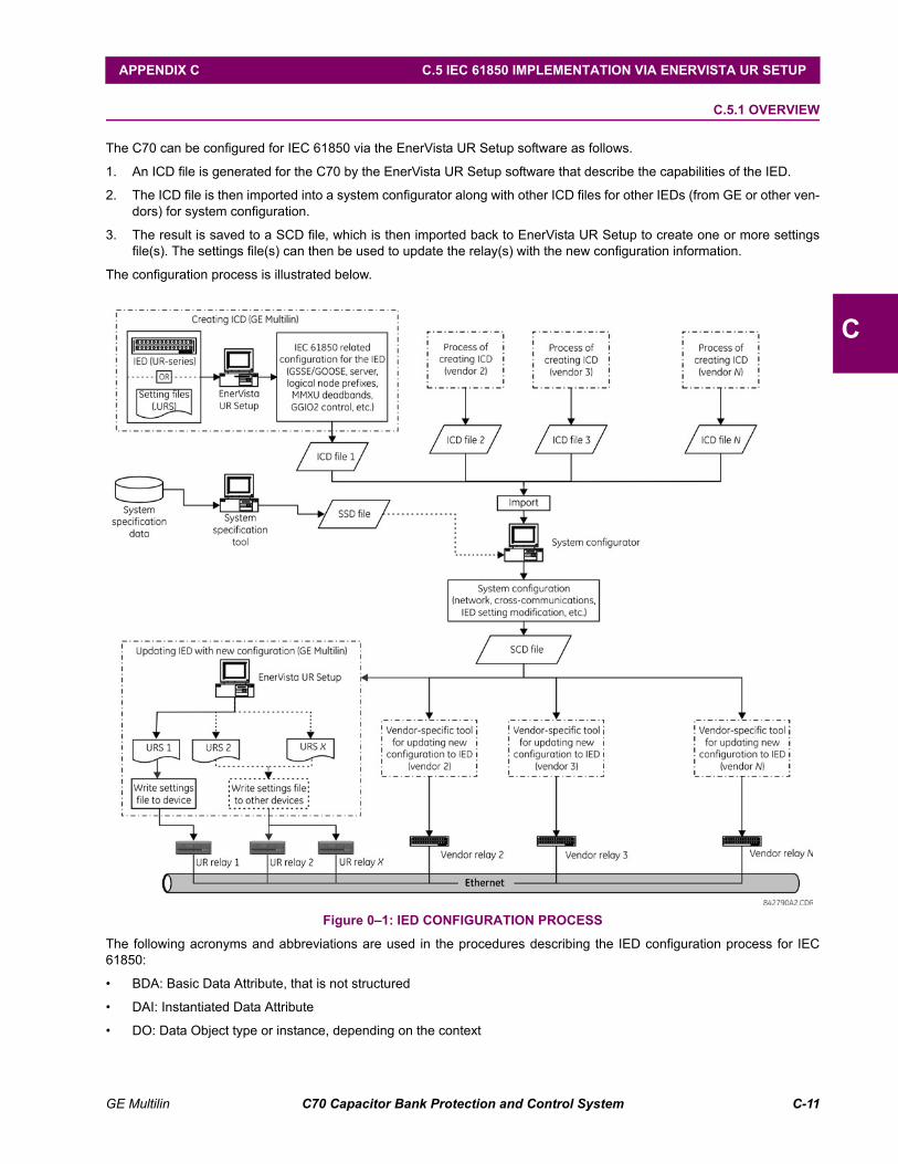
GE Multilin C70 Capacitor Bank Protection and Control System C-11
APPENDIX C C.5 IEC 61850 IMPLEMENTATION VIA ENERVISTA UR SETUP
C
C.5IEC 61850 IMPLEMENTATION VIA ENERVISTA UR SETUP C.5.1 OVERVIEW
The C70 can be configured for IEC 61850 via the EnerVista UR Setup software as follows.
1. An ICD file is generated for the C70 by the EnerVista UR Setup software that describe the capabilities of the IED.
2. The ICD file is then imported into a system configurator along with other ICD files for other IEDs (from GE or other ven-dors) for system configuration.
3. The result is saved to a SCD file, which is then imported back to EnerVista UR Setup to create one or more settingsfile(s). The settings file(s) can then be used to update the relay(s) with the new configuration information.
The configuration process is illustrated below.
Figure 0–1: IED CONFIGURATION PROCESS
The following acronyms and abbreviations are used in the procedures describing the IED configuration process for IEC61850:
• BDA: Basic Data Attribute, that is not structured
• DAI: Instantiated Data Attribute
• DO: Data Object type or instance, depending on the context

C-12 C70 Capacitor Bank Protection and Control System GE Multilin
C.5 IEC 61850 IMPLEMENTATION VIA ENERVISTA UR SETUP APPENDIX C
C
• DOI: Instantiated Data Object
• IED: Intelligent Electronic Device
• LDInst: Instantiated Logical Device
• LNInst: Instantiated Logical Node
• SCL: Substation Configuration Description Language. The configuration language is an application of the ExtensibleMarkup Language (XML) version 1.0.
• SDI: Instantiated Sub DATA; middle name part of a structured DATA name
• UR: GE Multilin Universal Relay series
• URI: Universal Resource Identifier
• URS: UR-series relay setting file
• XML: Extensible Markup Language
The following SCL variants are also used:
• ICD: IED Capability Description
• CID: Configured IED Description
• SSD: System Specification Description
• SCD: Substation Configuration Description
The following IEC related tools are referenced in the procedures that describe the IED configuration process for IEC 61850:
• System configurator or Substation configurator: This is an IED independent system level tool that can import orexport configuration files defined by IEC 61850-6. It can import configuration files (ICD) from several IEDs for systemlevel engineering and is used to add system information shared by different IEDs. The system configuration generatesa substation related configuration file (SCD) which is fed back to the IED configurator (for example, EnerVista URSetup) for system related IED configuration. The system configurator should also be able to read a system specifica-tion file (SSD) to use as base for starting system engineering, or to compare it with an engineered system for the samesubstation.
• IED configurator: This is a vendor specific tool that can directly or indirectly generate an ICD file from the IED (forexample, from a settings file). It can also import a system SCL file (SCD) to set communication configuration parame-ters (that is, required addresses, reception GOOSE datasets, IDs of incoming GOOSE datasets, etc.) for the IED. TheIED configurator functionality is implemented in the GE Multilin EnerVista UR Setup software.
C.5.2 CONFIGURING IEC 61850 SETTINGS
Before creating an ICD file, the user can customize the IEC 61850 related settings for the IED. For example, the IED nameand logical device instance can be specified to uniquely identify the IED within the substation, or transmission GOOSEdatasets created so that the system configurator can configure the cross-communication links to send GOOSE messagesfrom the IED. Once the IEC 61850 settings are configured, the ICD creation process will recognize the changes and gener-ate an ICD file that contains the updated settings.
Some of the IED settings will be modified during they system configuration process. For example, a new IP address may beassigned, line items in a Transmission GOOSE dataset may be added or deleted, or prefixes of some logical nodes may bechanged. While all new configurations will be mapped to the C70 settings file when importing an SCD file, all unchangedsettings will preserve the same values in the new settings file.
These settings can be configured either directly through the relay panel or through the EnerVista UR Setup software (pre-ferred method). The full list of IEC 61850 related settings for are as follows:
• Network configuration: IP address, IP subnet mask, and default gateway IP address (access through the Settings >Product Setup > Communications > Network menu tree in EnerVista UR Setup).
• Server configuration: IED name and logical device instance (access through the Settings > Product Setup > Com-munications > IEC 61850 > Server Configuration menu tree in EnerVista UR Setup).
• Logical node prefixes, which includes prefixes for all logical nodes except LLN0 (access through the Settings > Prod-uct Setup > Communications > IEC 61850 > Logical Node Prefixes menu tree in EnerVista UR Setup).
GE Multilin C70 Capacitor Bank Protection and Control System C-13
APPENDIX C C.5 IEC 61850 IMPLEMENTATION VIA ENERVISTA UR SETUP
C
• MMXU deadbands, which includes deadbands for all available MMXUs. The number of MMXUs is related to the num-ber of CT/VT modules in the relay. There are two MMXUs for each CT/VT module. For example, if a relay contains twoCT/VT modules, there will be four MMXUs available (access through the Settings > Product Setup > Communica-tions > IEC 61850 > MMXU Deadbands menu tree in EnerVista UR Setup).
• GGIO1 status configuration, which includes the number of status points in GGIO1 as well as the potential internal map-pings for each GGIO1 indication. However only the number of status points will be used in the ICD creation process(access through the Settings > Product Setup > Communications > IEC 61850 > GGIO1 Status Configurationmenu tree in EnerVista UR Setup).
• GGIO2 control configuration, which includes ctlModels for all SPCSOs within GGIO2 (access through the Settings >Product Setup > Communications > IEC 61850 > GGIO2 Control Configuration menu tree in EnerVista URSetup).
• Configurable transmission GOOSE, which includes eight configurable datasets that can be used for GOOSE transmis-sion. The GOOSE ID can be specified for each dataset (it must be unique within the IED as well as across the wholesubstation), as well as the destination MAC address, VLAN priority, VLAN ID, ETYPE APPID, and the dataset items.The selection of the dataset item is restricted by firmware version; for version 7.0x, only GGIO1.ST.Indx.stVal andGGIO1.ST.Indx.q are valid selection (where x is between 1 to N, and N is determined by number of GGIO1 statuspoints). Although configurable transmission GOOSE can also be created and altered by some third-party system con-figurators, we recommend configuring transmission GOOSE for GE Multilin IEDs before creating the ICD, and strictlywithin EnerVista UR Setup software or the front panel display (access through the Settings > Product Setup > Com-munications > IEC 61850 > GSSE/GOOSE Configuration > Transmission > Tx Configurable GOOSE menu treein EnerVista UR Setup).
• Configurable reception GOOSE, which includes eight configurable datasets that can be used for GOOSE reception.However, unlike datasets for transmission, datasets for reception only contains dataset items, and they are usually cre-ated automatically by process of importing the SCD file (access through the Settings > Product Setup > Communi-cations > IEC 61850 > GSSE/GOOSE Configuration > Reception > Rx Configurable GOOSE menu tree inEnerVista UR Setup).
• Remote devices configuration, which includes remote device ID (GOOSE ID or GoID of the incoming transmissionGOOSE dataset), ETYPE APPID (of the GSE communication block for the incoming transmission GOOSE), andDATASET (which is the name of the associated reception GOOSE dataset). These settings are usually done automat-ically by process of importing SCD file (access through the Settings > Inputs/Outputs > Remote Devices menu treein EnerVista UR Setup).
• Remote inputs configuration, which includes device (remote device ID) and item (which dataset item in the associatedreception GOOSE dataset to map) values. Only the items with cross-communication link created in SCD file should bemapped. These configurations are usually done automatically by process of importing SCD file (access through theSettings > Inputs/Outputs > Remote Inputs menu tree in EnerVista UR Setup).
C.5.3 ABOUT ICD FILES
The SCL language is based on XML, and its syntax definition is described as a W3C XML Schema. ICD is one type of SCLfile (which also includes SSD, CID and SCD files). The ICD file describes the capabilities of an IED and consists of fourmajor sections:
• Header
• Communication
• IEDs
• DataTypeTemplates
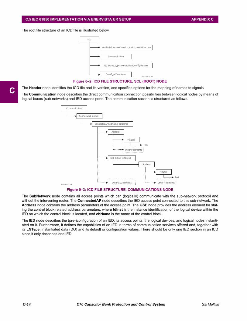
C-14 C70 Capacitor Bank Protection and Control System GE Multilin
C.5 IEC 61850 IMPLEMENTATION VIA ENERVISTA UR SETUP APPENDIX C
C
The root file structure of an ICD file is illustrated below.
Figure 0–2: ICD FILE STRUCTURE, SCL (ROOT) NODE
The Header node identifies the ICD file and its version, and specifies options for the mapping of names to signals
The Communication node describes the direct communication connection possibilities between logical nodes by means oflogical buses (sub-networks) and IED access ports. The communication section is structured as follows.
Figure 0–3: ICD FILE STRUCTURE, COMMUNICATIONS NODE
The SubNetwork node contains all access points which can (logically) communicate with the sub-network protocol andwithout the intervening router. The ConnectedAP node describes the IED access point connected to this sub-network. TheAddress node contains the address parameters of the access point. The GSE node provides the address element for stat-ing the control block related address parameters, where IdInst is the instance identification of the logical device within theIED on which the control block is located, and cbName is the name of the control block.
The IED node describes the (pre-)configuration of an IED: its access points, the logical devices, and logical nodes instanti-ated on it. Furthermore, it defines the capabilities of an IED in terms of communication services offered and, together withits LNType, instantiated data (DO) and its default or configuration values. There should be only one IED section in an ICDsince it only describes one IED.
842795A1.CDR
SCL
Header (id, version, revision, toolID, nameStructure)
Communication
IED (name, type, manufacture, configVersion)
DataTypeTemplates
842796A1.CDR
Communication
SubNetwork (name)
ConnectedAP (iedName, apName)
Address
GSE (IdInst, cbName)
P (type)
Other P elements
Text
Address
P (type)
Other P elements
Text
Other GSE elements

GE Multilin C70 Capacitor Bank Protection and Control System C-15
APPENDIX C C.5 IEC 61850 IMPLEMENTATION VIA ENERVISTA UR SETUP
C
Figure 0–4: ICD FILE STRUCTURE, IED NODE
842797A1.CDR
IED (name, type, manufacture, configVersion)
Services
AccessPoint (name)
DynAssoication
GetDirectory
GetDateObjectDefinition
DataObjectDirectory
GetDataSetValue
SetDataSetValue
DataSetDirectory
ConfDataSet (max, maxAttributes)
ReadWrite
TimerActivatedControl
ConfReportControl (max)
GetCBValues
ConfLogControl (max)
GSEDir
GOOSE (max)
GSSE (max)
Server
Authentication (none)
LDevice (inst)
LN0 (InType, InClass, inst)
DataSet (name)
Other DataSet elements
FCDA (fc, doName, daName, IdInst, prefix, InClass, InInst)
Other FCDA elements
DOI (name)
SDI (name)
Val Text
Other DOI elements
GSEControl (name, datSet, type, confRev, appID)
LN (InType, InClass, prefix, inst)
DataSet (name)
FCDA (IdInst, prefix, InClass, InInst, doName, fc)
Other FCDA elements
ReportControl (name, datSet, intgPd, rptID, confRev, buffered)
TrgOps (dchg) OptFields (seqNum) RptEnabled
Other ReportControl elements
Other GSEControl elements
ReportControl (name, datSet, intgPd, rptID, confRev, buffered)
RptEnabled
Other ReportControl elements
Other DataSet elements
Other LN elements
Other LDevice elements
DAI (name)
SDI (name)
Val
DAI (name)
Text
DOI (name)
SDI (name)
Val Text
Other DOI elements
DAI (name)
SDI (name)
Val
DAI (name)
Text
TrgOps (dchg) OptFields (seqNum)

C-16 C70 Capacitor Bank Protection and Control System GE Multilin
C.5 IEC 61850 IMPLEMENTATION VIA ENERVISTA UR SETUP APPENDIX C
C
The DataTypeTemplates node defines instantiable logical node types. A logical node type is an instantiable template of thedata of a logical node. A LnodeType is referenced each time that this instantiable type is needed with an IED. A logicalnode type template is built from DATA (DO) elements, which again have a DO type, which is derived from the DATA classes(CDC). DOs consist of attributes (DA) or of elements of already defined DO types (SDO). The attribute (DA) has a func-tional constraint, and can either have a basic type, be an enumeration, or a structure of a DAType. The DAType is built fromBDA elements, defining the structure elements, which again can be BDA elements of have a base type such as DA.
Figure 0–5: ICD FILE STRUCTURE, DATATYPETEMPLATES NODE
842798A1.CDR
DataTypeTemplates
LNodeType (id, InClass)
DO (name, type)
Other LNodeType elements
Other DO elements
DOType (id, cdc)
DA (name, fc, bType, type)
Other DOType elementsOther DOType elements
Other DA elements
DAType (id)
BDA (name, bType, type)
Other DAType elementsOther DAType elements
Other BDA elementsOther BDA elements
EnumType (id)
EnumVal (ord)
Other EnumType elements
Other EnumVal elements
Text
Val TextSDO (name, type)
Other SDO elements

GE Multilin C70 Capacitor Bank Protection and Control System C-17
APPENDIX C C.5 IEC 61850 IMPLEMENTATION VIA ENERVISTA UR SETUP
C
C.5.4 CREATING AN ICD FILE WITH ENERVISTA UR SETUP
An ICD file can be created directly from a connected C70 IED or from an offline C70 settings file with the EnerVista URSetup software using the following procedure:
1. Right-click the connected UR-series relay or settings file and select Create ICD File.
2. The EnerVista UR Setup will prompt to save the file. Select the file path and enter the name for the ICD file, then clickOK to generate the file.
The time to create an ICD file from the offline C70 settings file is typically much quicker than create an ICD file directly fromthe relay.
C.5.5 ABOUT SCD FILES
System configuration is performed in the system configurator. While many vendors (including GE Multilin) are working theirown system configuration tools, there are some system configurators available in the market (for example, Siemens DIGSIversion 4.6 or above and ASE Visual SCL Beta 0.12).
Although the configuration tools vary from one vendor to another, the procedure is pretty much the same. First, a substationproject must be created, either as an empty template or with some system information by importing a system specificationfile (SSD). Then, IEDs are added to the substation. Since each IED is represented by its associated ICD, the ICD files areimported into the substation project, and the system configurator validates the ICD files during the importing process. If theICD files are successfully imported into the substation project, it may be necessary to perform some additional minor stepsto attach the IEDs to the substation (see the system configurator manual for details).
Once all IEDs are inserted into the substation, further configuration is possible, such as:
• Assigning network addresses to individual IEDs.
• Customizing the prefixes of logical nodes.
• Creating cross-communication links (configuring GOOSE messages to send from one IED to others).
When system configurations are complete, the results are saved to an SCD file, which contains not only the configurationfor each IED in the substation, but also the system configuration for the entire substation. Finally, the SCD file is passedback to the IED configurator (vendor specific tool) to update the new configuration into the IED.
The SCD file consists of at least five major sections:

C-18 C70 Capacitor Bank Protection and Control System GE Multilin
C.5 IEC 61850 IMPLEMENTATION VIA ENERVISTA UR SETUP APPENDIX C
C
• Header.
• Substation.
• Communication.
• IED section (one or more).
• DataTypeTemplates.
The root file structure of an SCD file is illustrated below.
Figure 0–6: SCD FILE STRUCTURE, SCL (ROOT) NODE
Like ICD files, the Header node identifies the SCD file and its version, and specifies options for the mapping of names tosignals.
The Substation node describes the substation parameters:
Figure 0–7: SCD FILE STRUCTURE, SUBSTATION NODE
842791A1.CDR
SCL
Header (id, version, revision, toolID, nameStructure)
IED Section (IED 2)
Communication
IED Section (IED 1)
Substation
Other IED Sections
DataTypeTemplates
842792A1.CDR
Substation
EquipmentContainer
VoltageLevel
Function
PowerSystemResource
Power Transformer
GeneralEquipment
EquipmentContainer
Bay
Voltage
PowerSystemResource
SubFunction
GeneralEquipment

GE Multilin C70 Capacitor Bank Protection and Control System C-19
APPENDIX C C.5 IEC 61850 IMPLEMENTATION VIA ENERVISTA UR SETUP
C
The Communication node describes the direct communication connection possibilities between logical nodes by means oflogical buses (sub-networks) and IED access ports. The communication section is structured as follows.
Figure 0–8: SCD FILE STRUCTURE, COMMUNICATIONS NODE
The SubNetwork node contains all access points which can (logically) communicate with the sub-network protocol andwithout the intervening router. The ConnectedAP node describes the IED access point connected to this sub-network. TheAddress node contains the address parameters of the access point. The GSE node provides the address element for stat-ing the control block related address parameters, where IdInst is the instance identification of the logical device within theIED on which the control block is located, and cbName is the name of the control block.
842793A1.CDR
Communication
SubNetwork (name)
ConnectedAP (IED 1)
Address
GSE (IdInst, cbName)
P (type)
Other P elements
Text
Address
P (type)
Other P elements
TextOther GSE elements
ConnectedAP (IED 2)
Address
GSE (IdInst, cbName)
P (type)
Other P elements
Text
Address
P (type)
Text
Other GSE elements
Other ConnectedAP elements
Other P elements

C-20 C70 Capacitor Bank Protection and Control System GE Multilin
C.5 IEC 61850 IMPLEMENTATION VIA ENERVISTA UR SETUP APPENDIX C
C
The IED Section node describes the configuration of an IED.
Figure 0–9: SCD FILE STRUCTURE, IED NODE
C.5.6 IMPORTING AN SCD FILE WITH ENERVISTA UR SETUP
The following procedure describes how to update the C70 with the new configuration from an SCD file with the EnerVistaUR Setup software.
1. Right-click anywhere in the files panel and select the Import Contents From SCD File item.
2. Select the saved SCD file and click Open.
842794A1.CDR
IED Section (IED 1)
AccessPoint (name)
Server
Authentication (none)
LDevice (inst)
LN0 (InType, InClass, inst)
DataSet elements
DOI elements
Inputs
GSEControl elements
ReportControl elements
ExtRef (iedName, ldInst, prefix, lnClass, lnInst, doName, daName, intAddr)
Other ExtRef elements

GE Multilin C70 Capacitor Bank Protection and Control System C-21
APPENDIX C C.5 IEC 61850 IMPLEMENTATION VIA ENERVISTA UR SETUP
C
3. The software will open the SCD file and then prompt the user to save a UR-series settings file. Select a location andname for the URS (UR-series relay settings) file.
If there is more than one GE Multilin IED defined in the SCD file, the software prompt the user to save a UR-series set-tings file for each IED.
4. After the URS file is created, modify any settings (if required).
5. To update the relay with the new settings, right-click on the settings file in the settings tree and select the Write Set-tings File to Device item.
6. The software will prompt for the target device. Select the target device from the list provided and click Send. The newsettings will be updated to the selected device.
C-22 C70 Capacitor Bank Protection and Control System GE Multilin
C.6 ACSI CONFORMANCE APPENDIX C
C
C.6ACSI CONFORMANCE C.6.1 ACSI BASIC CONFORMANCE STATEMENT
c1: shall be "M" if support for LOGICAL-DEVICE model has been declaredO: OptionalM: Mandatory
C.6.2 ACSI MODELS CONFORMANCE STATEMENT
SERVICES SERVER/PUBLISHER
UR-FAMILY
CLIENT-SERVER ROLES
B11 Server side (of Two-party Application-Association) c1 Yes
B12 Client side (of Two-party Application-Association) ---
SCSMS SUPPORTED
B21 SCSM: IEC 61850-8-1 used Yes
B22 SCSM: IEC 61850-9-1 used
B23 SCSM: IEC 61850-9-2 used
B24 SCSM: other
GENERIC SUBSTATION EVENT MODEL (GSE)
B31 Publisher side O Yes
B32 Subscriber side --- Yes
TRANSMISSION OF SAMPLED VALUE MODEL (SVC)
B41 Publisher side O
B42 Subscriber side ---
SERVICES SERVER/PUBLISHER
UR-FAMILY
IF SERVER SIDE (B11) SUPPORTED
M1 Logical device c2 Yes
M2 Logical node c3 Yes
M3 Data c4 Yes
M4 Data set c5 Yes
M5 Substitution O
M6 Setting group control O
REPORTING
M7 Buffered report control O Yes
M7-1 sequence-number
M7-2 report-time-stamp
M7-3 reason-for-inclusion
M7-4 data-set-name
M7-5 data-reference
M7-6 buffer-overflow
M7-7 entryID
M7-8 BufTm
M7-9 IntgPd
M7-10 GI
M8 Unbuffered report control O Yes
M8-1 sequence-number
M8-2 report-time-stamp
M8-3 reason-for-inclusion
NOTE

GE Multilin C70 Capacitor Bank Protection and Control System C-23
APPENDIX C C.6 ACSI CONFORMANCE
C
c2: shall be "M" if support for LOGICAL-NODE model has been declaredc3: shall be "M" if support for DATA model has been declaredc4: shall be "M" if support for DATA-SET, Substitution, Report, Log Control, or Time models has been declaredc5: shall be "M" if support for Report, GSE, or SMV models has been declaredM: Mandatory
C.6.3 ACSI SERVICES CONFORMANCE STATEMENT
In the table below, the acronym AA refers to Application Associations (TP: Two Party / MC: Multicast). The c6 to c10 entriesare defined in the notes following the table.
M8-4 data-set-name
M8-5 data-reference
M8-6 BufTm
M8-7 IntgPd
M8-8 GI
Logging O
M9 Log control O
M9-1 IntgPd
M10 Log O
M11 Control M Yes
IF GSE (B31/32) IS SUPPORTED
GOOSE O Yes
M12-1 entryID
M12-2 DataReflnc
M13 GSSE O Yes
IF SVC (B41/B42) IS SUPPORTED
M14 Multicast SVC O
M15 Unicast SVC O
M16 Time M Yes
M17 File transfer O Yes
SERVICES AA: TP/MC SERVER/ PUBLISHER
UR FAMILY
SERVER (CLAUSE 7)
S1 ServerDirectory TP M Yes
APPLICATION ASSOCIATION (CLAUSE 8)
S2 Associate TP M Yes
S3 Abort TP M Yes
S4 Release TP M Yes
LOGICAL DEVICE (CLAUSE 9)
S5 LogicalDeviceDirectory TP M Yes
LOGICAL NODE (CLAUSE 10)
S6 LogicalNodeDirectory TP M Yes
S7 GetAllDataValues TP M Yes
DATA (CLAUSE 11)
S8 GetDataValues TP M Yes
S9 SetDataValues TP O Yes
S10 GetDataDirectory TP M Yes
S11 GetDataDefinition TP M Yes
SERVICES SERVER/PUBLISHER
UR-FAMILY
NOTE

C-24 C70 Capacitor Bank Protection and Control System GE Multilin
C.6 ACSI CONFORMANCE APPENDIX C
C
DATA SET (CLAUSE 12)
S12 GetDataSetValues TP M Yes
S13 SetDataSetValues TP O
S14 CreateDataSet TP O
S15 DeleteDataSet TP O
S16 GetDataSetDirectory TP O Yes
SETTING GROUP CONTROL (CLAUSE 16)
S18 SelectActiveSG TP O
S19 SelectEditSG TP O
S20 SetSGValues TP O
S21 ConfirmEditSGValues TP O
S22 GetSGValues TP O
S23 GetSGCBValues TP O
REPORTING (CLAUSE 17)
BUFFERED REPORT CONTROL BLOCK (BRCB)
S24 Report TP c6 Yes
S24-1 data-change (dchg) Yes
S24-2 qchg-change (qchg)
S24-3 data-update (dupd)
S25 GetBRCBValues TP c6 Yes
S26 SetBRCBValues TP c6 Yes
UNBUFFERED REPORT CONTROL BLOCK (URCB)
S27 Report TP c6 Yes
S27-1 data-change (dchg) Yes
S27-2 qchg-change (qchg)
S27-3 data-update (dupd)
S28 GetURCBValues TP c6 Yes
S29 SetURCBValues TP c6 Yes
LOGGING (CLAUSE 17)
LOG CONTROL BLOCK
S30 GetLCBValues TP M
S31 SetLCBValues TP M
LOG
S32 QueryLogByTime TP M
S33 QueryLogByEntry TP M
S34 GetLogStatusValues TP M
GENERIC SUBSTATION EVENT MODEL (GSE) (CLAUSE 18, ANNEX C)
GOOSE-CONTROL-BLOCK (CLAUSE 18)
S35 SendGOOSEMessage MC c8 Yes
S36 GetReference TP c9
S37 GetGOOSEElementNumber TP c9
S38 GetGoCBValues TP O Yes
S39 SetGoCBValues TP O Yes
GSSE-CONTROL-BLOCK (ANNEX C)
S40 SendGSSEMessage MC c8 Yes
S41 GetReference TP c9
S42 GetGSSEElementNumber TP c9
S43 GetGsCBValues TP O Yes
SERVICES AA: TP/MC SERVER/ PUBLISHER
UR FAMILY

GE Multilin C70 Capacitor Bank Protection and Control System C-25
APPENDIX C C.6 ACSI CONFORMANCE
C
c6: shall declare support for at least one (BRCB or URCB)c7: shall declare support for at least one (QueryLogByTime or QueryLogAfter)c8: shall declare support for at least one (SendGOOSEMessage or SendGSSEMessage)c9: shall declare support if TP association is availablec10: shall declare support for at least one (SendMSVMessage or SendUSVMessage)
S44 SetGsCBValues TP O Yes
TRANSMISSION OF SAMPLED VALUE MODEL (SVC) (CLAUSE 19)
MULTICAST SVC
S45 SendMSVMessage MC c10
S46 GetMSVCBValues TP O
S47 SetMSVCBValues TP O
UNICAST SVC
S48 SendUSVMessage MC c10
S49 GetUSVCBValues TP O
S50 SetUSVCBValues TP O
CONTROL (CLAUSE 20)
S51 Select O Yes
S52 SelectWithValue TP O
S53 Cancel TP O Yes
S54 Operate TP M Yes
S55 Command-Termination TP O
S56 TimeActivated-Operate TP O
FILE TRANSFER (CLAUSE 23)
S57 GetFile TP M Yes
S58 SetFile TP O
S59 DeleteFile TP O
S60 GetFileAttributeValues TP M Yes
TIME (CLAUSE 5.5)
T1 Time resolution of internal clock (nearest negative power of 2 in seconds)
20
T2 Time accuracy of internal clock SNTP, IRIG-B
T3 Supported TimeStamp resolution (nearest value of 2–n in seconds, according to 6.1.2.9.3.2)
20
SERVICES AA: TP/MC SERVER/ PUBLISHER
UR FAMILY
NOTE

C-26 C70 Capacitor Bank Protection and Control System GE Multilin
C.7 LOGICAL NODES APPENDIX C
C
C.7LOGICAL NODES C.7.1 LOGICAL NODES TABLE
The UR-series of relays supports IEC 61850 logical nodes as indicated in the following table. Note that the actual instantia-tion of each logical node is determined by the product order code. For example. the logical node “PDIS” (distance protec-tion) is available only in the D60 Line Distance Relay.
Table C–1: IEC 61850 LOGICAL NODES (Sheet 1 of 4)
NODES UR-FAMILY
L: SYSTEM LOGICAL NODES
LPHD: Physical device information Yes
LLN0: Logical node zero Yes
LCCH: Physical communication channel supervision ---
LGOS: GOOSE subscription ---
LSVS: Sampled value subscription ---
LTIM: Time management ---
LTMS: Time master supervision ---
LTRK: Service tracking ---
A: LOGICAL NODES FOR AUTOMATIC CONTROL
ANCR: Neutral current regulator ---
ARCO: Reactive power control ---
ATCC: Automatic tap changer controller ---
AVCO: Voltage control ---
C: LOGICAL NODES FOR CONTROL
CALH: Alarm handling ---
CCGR: Cooling group control ---
CILO: Interlocking ---
CPOW: Point-on-wave switching ---
CSWI: Switch controller Yes
CSYN: Synchronizer controller ---
F: LOGICAL NODES FOR FUNCTIONAL BLOCKS
FCNT: Counter ---
FCSD: Curve shape description ---
FFIL: Generic filler ---
FLIM: Control function output limitation ---
FPID: PID regulator ---
FRMP: Ramp function ---
FSPT: Set-point control function ---
FXOT: Action at over threshold ---
FXUT: Action at under threshold ---
G: LOGICAL NODES FOR GENERIC REFERENCES
GAPC: Generic automatic process control ---
GGIO: Generic process I/O Yes
GLOG: Generic log ---
GSAL: Generic security application ---
I: LOGICAL NODES FOR INTERFACING AND ARCHIVING
IARC: Archiving ---
IHMI: Human machine interface ---
ISAF: Safety alarm function ---
ITCI: Telecontrol interface ---
ITMI: Telemonitoring interface ---

GE Multilin C70 Capacitor Bank Protection and Control System C-27
APPENDIX C C.7 LOGICAL NODES
C
ITPC: Teleprotection communication interfaces ---
K: LOGICAL NODES FOR MECHANICAL AND NON-ELECTRIC PRIMARY EQUIPMENT
KFAN: Fan ---
KFIL: Filter ---
KPMP: Pump ---
KTNK: Tank ---
KVLV: Valve control ---
M: LOGICAL NODES FOR METERING AND MEASUREMENT
MENV: Environmental information ---
MFLK: Flicker measurement name ---
MHAI: Harmonics or interharmonics ---
MHAN: Non phase related harmonics or interharmonics ---
MHYD: Hydrological information ---
MMDC: DC measurement ---
MMET: Meteorological information ---
MMTN: Metering ---
MMTR: Metering ---
MMXN: Non-phase-related measurement Yes
MMXU: Measurement Yes
MSQI: Sequence and imbalance Yes
MSTA: Metering statistics ---
P: LOGICAL NODES FOR PROTECTION FUNCTIONS
PDIF: Differential Yes
PDIR: Direction comparison ---
PDIS: Distance Yes
PDOP: Directional overpower ---
PDUP: Directional underpower ---
PFRC: Rate of change of frequency ---
PHAR: Harmonic restraint ---
PHIZ: Ground detector ---
PIOC: Instantaneous overcurrent Yes
PMRI Motor restart inhibition ---
PMSS: Motor starting time supervision ---
POPF: Over power factor ---
PPAM: Phase angle measuring ---
PRTR: Rotor protection ---
PSCH: Protection scheme ---
PSDE: Sensitive directional earth fault ---
PTEF: Transient earth fault ---
PTOC: Time overcurrent Yes
PTOF: Overfrequency ---
PTOV: Overvoltage Yes
PTRC: Protection trip conditioning Yes
PTTR: Thermal overload ---
PTUC: Undercurrent ---
PTUF: Underfrequency ---
PTUV: Undervoltage Yes
Table C–1: IEC 61850 LOGICAL NODES (Sheet 2 of 4)
NODES UR-FAMILY
C-28 C70 Capacitor Bank Protection and Control System GE Multilin
C.7 LOGICAL NODES APPENDIX C
C
PUPF: Underpower factor ---
PVOC: Voltage controlled time overcurrent ---
PVPH: Volts per Hz ---
PZSU: Zero speed or underspeed ---
Q: LOGICAL NODES FOR POWER QUALITY EVENTS
QFVR: Frequency variation ---
QITR: Current transient ---
QIUB: Current unbalance variation ---
QVTR: Voltage transient ---
QVUB: Voltage unbalance variation ---
QVVR: Voltage variation ---
R: LOGICAL NODES FOR PROTECTION-RELATED FUNCTIONS
RADR: Disturbance recorder channel analogue ---
RBDR: Disturbance recorder channel binary ---
RBRF: Breaker failure ---
RDIR: Directional element ---
RDRE: Disturbance recorder function ---
RDRS: Disturbance record handling ---
RFLO: Fault locator Yes
RMXU: Differential measurements ---
RPSB: Power swing detection/blocking Yes
RREC: Autoreclosing Yes
RSYN: Synchronism-check or synchronizing ---
S: LOGICAL NODES FOR SENSORS AND MONITORING
SARC: Monitoring and diagnostics for arcs ---
SCBR: Circuit breaker supervision ---
SIMG: Insulation medium supervision (gas) ---
SIML: Insulation medium supervision (liquid) ---
SLTC: Tap changer supervision ---
SOPM: Supervision of operating mechanism ---
SPDC: Monitoring and diagnostics for partial discharges ---
SPTR: Power transformer supervision ---
SSWI: Circuit switch supervision ---
STMP: Temperature supervision ---
SVBR: Vibration supervision ---
T: LOGICAL NODES FOR INSTRUMENT TRANSFORMERS
TANG: Angle ---
TAXD: Axial displacement ---
TCTR: Current transformer ---
TDST: Distance ---
TFLW: Liquid flow ---
TFRQ: Frequency ---
TGSN: Generic sensor ---
THUM: Humidity ---
TLVL: Media level ---
TMGF: Magnetic field ---
TMVM: Movement sensor ---
Table C–1: IEC 61850 LOGICAL NODES (Sheet 3 of 4)
NODES UR-FAMILY

GE Multilin C70 Capacitor Bank Protection and Control System C-29
APPENDIX C C.7 LOGICAL NODES
C
TPOS: Position indicator ---
TPRS: Pressure sensor ---
TRTN: Rotation transmitter ---
TSND: Sound pressure sensor ---
TTMP: Temperature sensor ---
TTNS: Mechanical tension ---
TVBR: Vibration sensor ---
TVTR: Voltage transformer ---
TWPH: Water acidity ---
X: LOGICAL NODES FOR SWITCHGEAR
XCBR: Circuit breaker Yes
XSWI: Circuit switch Yes
Y: LOGICAL NODES FOR POWER TRANSFORMERS
YEFN: Earth fault neutralizer (Petersen coil) ---
YLTC: Tap changer ---
YPSH: Power shunt ---
YPTR: Power transformer ---
Z: LOGICAL NODES FOR FURTHER POWER SYSTEM EQUIPMENT
ZAXN: Auxiliary network ---
ZBAT: Battery ---
ZBSH: Bushing ---
ZCAB: Power cable ---
ZCAP: Capacitor bank ---
ZCON: Converter ---
ZGEN: Generator ---
ZGIL: Gas insulated line ---
ZLIN: Power overhead line ---
ZMOT: Motor ---
ZREA: Reactor ---
ZRES: Resistor ---
ZRRC: Rotating reactive component ---
ZSAR: Surge arrestor ---
ZSCR: Semi-conductor controlled rectifier ---
ZSMC: Synchronous machine ---
ZTCF: Thyristor controlled frequency converter ---
ZTRC: Thyristor controlled reactive component ---
Table C–1: IEC 61850 LOGICAL NODES (Sheet 4 of 4)
NODES UR-FAMILY

C-30 C70 Capacitor Bank Protection and Control System GE Multilin
C.7 LOGICAL NODES APPENDIX C
C

GE Multilin C70 Capacitor Bank Protection and Control System D-1
APPENDIX D D.1 OVERVIEW
D
APPENDIX D IEC 60870-5-104 COMMUNICATIONSD.1OVERVIEW D.1.1 INTEROPERABILITY DOCUMENT
This document is adapted from the IEC 60870-5-104 standard. For this section the boxes indicate the following: – usedin standard direction; – not used; – cannot be selected in IEC 60870-5-104 standard.
1. SYSTEM OR DEVICE:
System Definition
Controlling Station Definition (Master)
Controlled Station Definition (Slave)
2. NETWORK CONFIGURATION:
Point-to-Point Multipoint
Multiple Point-to-Point Multipoint Star
3. PHYSICAL LAYER
Transmission Speed (control direction):
Transmission Speed (monitor direction):
4. LINK LAYER
Unbalanced InterchangeCircuit V.24/V.28 Standard:
Unbalanced InterchangeCircuit V.24/V.28 Recommendedif >1200 bits/s:
Balanced Interchange CircuitX.24/X.27:
100 bits/sec.
200 bits/sec.
300 bits/sec.
600 bits/sec.
1200 bits/sec.
2400 bits/sec.
4800 bits/sec.
9600 bits/sec.
2400 bits/sec.
4800 bits/sec.
9600 bits/sec.
19200 bits/sec.
38400 bits/sec.
56000 bits/sec.
64000 bits/sec.
Link Transmission Procedure: Address Field of the Link:
Balanced Transmission
Unbalanced Transmission
Not Present (Balanced Transmission Only)
One Octet
Two Octets
Structured
Unstructured
Frame Length (maximum length, number of octets): Not selectable in companion IEC 60870-5-104 standard

D-2 C70 Capacitor Bank Protection and Control System GE Multilin
D.1 OVERVIEW APPENDIX D
D
When using an unbalanced link layer, the following ADSU types are returned in class 2 messages (low priority) with theindicated causes of transmission:
The standard assignment of ADSUs to class 2 messages is used as follows:
A special assignment of ADSUs to class 2 messages is used as follows:
5. APPLICATION LAYER
Transmission Mode for Application Data:Mode 1 (least significant octet first), as defined in Clause 4.10 of IEC 60870-5-4, is used exclusively in this companionstandard.
Common Address of ADSU:
One Octet
Two Octets
Information Object Address:
One Octet Structured
Two Octets Unstructured
Three Octets
Cause of Transmission:
One Octet
Two Octets (with originator address). Originator address is set to zero if not used.
Maximum Length of APDU: 253 (the maximum length may be reduced by the system.
Selection of standard ASDUs:
For the following lists, the boxes indicate the following: – used in standard direction; – not used; – cannot beselected in IEC 60870-5-104 standard.
Process information in monitor direction
<1> := Single-point information M_SP_NA_1
<2> := Single-point information with time tag M_SP_TA_1
<3> := Double-point information M_DP_NA_1
<4> := Double-point information with time tag M_DP_TA_1
<5> := Step position information M_ST_NA_1
<6> := Step position information with time tag M_ST_TA_1
<7> := Bitstring of 32 bits M_BO_NA_1
<8> := Bitstring of 32 bits with time tag M_BO_TA_1
<9> := Measured value, normalized value M_ME_NA_1
<10> := Measured value, normalized value with time tag M_NE_TA_1
<11> := Measured value, scaled value M_ME_NB_1
<12> := Measured value, scaled value with time tag M_NE_TB_1
<13> := Measured value, short floating point value M_ME_NC_1
<14> := Measured value, short floating point value with time tag M_NE_TC_1
<15> := Integrated totals M_IT_NA_1
<16> := Integrated totals with time tag M_IT_TA_1
<17> := Event of protection equipment with time tag M_EP_TA_1
<18> := Packed start events of protection equipment with time tag M_EP_TB_1
<19> := Packed output circuit information of protection equipment with time tag M_EP_TC_1
<20> := Packed single-point information with status change detection M_SP_NA_1

GE Multilin C70 Capacitor Bank Protection and Control System D-3
APPENDIX D D.1 OVERVIEW
D
Either the ASDUs of the set <2>, <4>, <6>, <8>, <10>, <12>, <14>, <16>, <17>, <18>, and <19> or of the set<30> to <40> are used.
Process information in control direction
Either the ASDUs of the set <45> to <51> or of the set <58> to <64> are used.
System information in monitor direction
System information in control direction
<21> := Measured value, normalized value without quantity descriptor M_ME_ND_1
<30> := Single-point information with time tag CP56Time2a M_SP_TB_1
<31> := Double-point information with time tag CP56Time2a M_DP_TB_1
<32> := Step position information with time tag CP56Time2a M_ST_TB_1
<33> := Bitstring of 32 bits with time tag CP56Time2a M_BO_TB_1
<34> := Measured value, normalized value with time tag CP56Time2a M_ME_TD_1
<35> := Measured value, scaled value with time tag CP56Time2a M_ME_TE_1
<36> := Measured value, short floating point value with time tag CP56Time2a M_ME_TF_1
<37> := Integrated totals with time tag CP56Time2a M_IT_TB_1
<38> := Event of protection equipment with time tag CP56Time2a M_EP_TD_1
<39> := Packed start events of protection equipment with time tag CP56Time2a M_EP_TE_1
<40> := Packed output circuit information of protection equipment with time tag CP56Time2a M_EP_TF_1
<45> := Single command C_SC_NA_1
<46> := Double command C_DC_NA_1
<47> := Regulating step command C_RC_NA_1
<48> := Set point command, normalized value C_SE_NA_1
<49> := Set point command, scaled value C_SE_NB_1
<50> := Set point command, short floating point value C_SE_NC_1
<51> := Bitstring of 32 bits C_BO_NA_1
<58> := Single command with time tag CP56Time2a C_SC_TA_1
<59> := Double command with time tag CP56Time2a C_DC_TA_1
<60> := Regulating step command with time tag CP56Time2a C_RC_TA_1
<61> := Set point command, normalized value with time tag CP56Time2a C_SE_TA_1
<62> := Set point command, scaled value with time tag CP56Time2a C_SE_TB_1
<63> := Set point command, short floating point value with time tag CP56Time2a C_SE_TC_1
<64> := Bitstring of 32 bits with time tag CP56Time2a C_BO_TA_1
<70> := End of initialization M_EI_NA_1
<100> := Interrogation command C_IC_NA_1
<101> := Counter interrogation command C_CI_NA_1
<102> := Read command C_RD_NA_1
<103> := Clock synchronization command (see Clause 7.6 in standard) C_CS_NA_1
<104> := Test command C_TS_NA_1
<105> := Reset process command C_RP_NA_1
<106> := Delay acquisition command C_CD_NA_1
<107> := Test command with time tag CP56Time2a C_TS_TA_1

D-4 C70 Capacitor Bank Protection and Control System GE Multilin
D.1 OVERVIEW APPENDIX D
D
Parameter in control direction
File transfer
Type identifier and cause of transmission assignments(station-specific parameters)
In the following table:
•Shaded boxes are not required.
•Black boxes are not permitted in this companion standard.
•Blank boxes indicate functions or ASDU not used.
•‘X’ if only used in the standard direction
<110> := Parameter of measured value, normalized value PE_ME_NA_1
<111> := Parameter of measured value, scaled value PE_ME_NB_1
<112> := Parameter of measured value, short floating point value PE_ME_NC_1
<113> := Parameter activation PE_AC_NA_1
<120> := File Ready F_FR_NA_1
<121> := Section Ready F_SR_NA_1
<122> := Call directory, select file, call file, call section F_SC_NA_1
<123> := Last section, last segment F_LS_NA_1
<124> := Ack file, ack section F_AF_NA_1
<125> := Segment F_SG_NA_1
<126> := Directory (blank or X, available only in monitor [standard] direction) C_CD_NA_1
TYPE IDENTIFICATION CAUSE OF TRANSMISSION
NO. MNEMONIC 1 2 3 4 5 6 7 8 9 10 11 12 1320 to 36
37 to 41
44 45 46 47
<1> M_SP_NA_1 X X X X X
<2> M_SP_TA_1
<3> M_DP_NA_1
<4> M_DP_TA_1
<5> M_ST_NA_1
<6> M_ST_TA_1
<7> M_BO_NA_1
<8> M_BO_TA_1
<9> M_ME_NA_1
PE
RIO
DIC
, CY
CL
IC
BA
CK
GR
OU
ND
SC
AN
SP
ON
TA
NE
OU
S
INIT
IAL
IZE
D
RE
QU
ES
T O
R R
EQ
UE
ST
ED
AC
TIV
AT
ION
AC
TIV
AT
ION
CO
NF
IRM
AT
ION
DE
AC
TIV
AT
ION
DE
AC
TIV
AT
ION
CO
NF
IRM
AT
ION
AC
TIV
AT
ION
TE
RM
INA
TIO
N
RE
TU
RN
INF
O C
AU
SE
D B
Y L
OC
AL
CM
D
FIL
E T
RA
NS
FE
R
INT
ER
RO
GA
TE
D B
Y G
RO
UP
<N
UM
BE
R>
RE
QU
ES
T B
Y G
RO
UP
<N
> C
OU
NT
ER
RE
Q
UN
KN
OW
N T
YP
E ID
EN
TIF
ICA
TIO
N
UN
KN
OW
N C
AU
SE
OF
TR
AN
SM
ISS
ION
UN
KN
OW
N C
OM
MO
N A
DD
RE
SS
OF
AD
SU
UN
KN
OW
N IN
FO
RM
AT
ION
OB
JEC
T A
DD
R
UN
KN
OW
N IN
FO
RM
AT
ION
OB
JEC
T A
DD
R

GE Multilin C70 Capacitor Bank Protection and Control System D-5
APPENDIX D D.1 OVERVIEW
D<10> M_ME_TA_1
<11> M_ME_NB_1
<12> M_ME_TB_1
<13> M_ME_NC_1 X X X X
<14> M_ME_TC_1
<15> M_IT_NA_1 X X
<16> M_IT_TA_1
<17> M_EP_TA_1
<18> M_EP_TB_1
<19> M_EP_TC_1
<20> M_PS_NA_1
<21> M_ME_ND_1
<30> M_SP_TB_1 X X X
<31> M_DP_TB_1
<32> M_ST_TB_1
<33> M_BO_TB_1
<34> M_ME_TD_1
<35> M_ME_TE_1
<36> M_ME_TF_1
<37> M_IT_TB_1 X X
<38> M_EP_TD_1
<39> M_EP_TE_1
<40> M_EP_TF_1
<45> C_SC_NA_1 X X X X X
<46> C_DC_NA_1
<47> C_RC_NA_1
<48> C_SE_NA_1
<49> C_SE_NB_1
<50> C_SE_NC_1
<51> C_BO_NA_1
<58> C_SC_TA_1 X X X X X
<59> C_DC_TA_1
<60> C_RC_TA_1
TYPE IDENTIFICATION CAUSE OF TRANSMISSION
NO. MNEMONIC 1 2 3 4 5 6 7 8 9 10 11 12 1320 to 36
37 to 41
44 45 46 47
PE
RIO
DIC
, CY
CL
IC
BA
CK
GR
OU
ND
SC
AN
SP
ON
TA
NE
OU
S
INIT
IAL
IZE
D
RE
QU
ES
T O
R R
EQ
UE
ST
ED
AC
TIV
AT
ION
AC
TIV
AT
ION
CO
NF
IRM
AT
ION
DE
AC
TIV
AT
ION
DE
AC
TIV
AT
ION
CO
NF
IRM
AT
ION
AC
TIV
AT
ION
TE
RM
INA
TIO
N
RE
TU
RN
INF
O C
AU
SE
D B
Y L
OC
AL
CM
D
FIL
E T
RA
NS
FE
R
INT
ER
RO
GA
TE
D B
Y G
RO
UP
<N
UM
BE
R>
RE
QU
ES
T B
Y G
RO
UP
<N
> C
OU
NT
ER
RE
Q
UN
KN
OW
N T
YP
E ID
EN
TIF
ICA
TIO
N
UN
KN
OW
N C
AU
SE
OF
TR
AN
SM
ISS
ION
UN
KN
OW
N C
OM
MO
N A
DD
RE
SS
OF
AD
SU
UN
KN
OW
N IN
FO
RM
AT
ION
OB
JEC
T A
DD
R
UN
KN
OW
N IN
FO
RM
AT
ION
OB
JEC
T A
DD
R
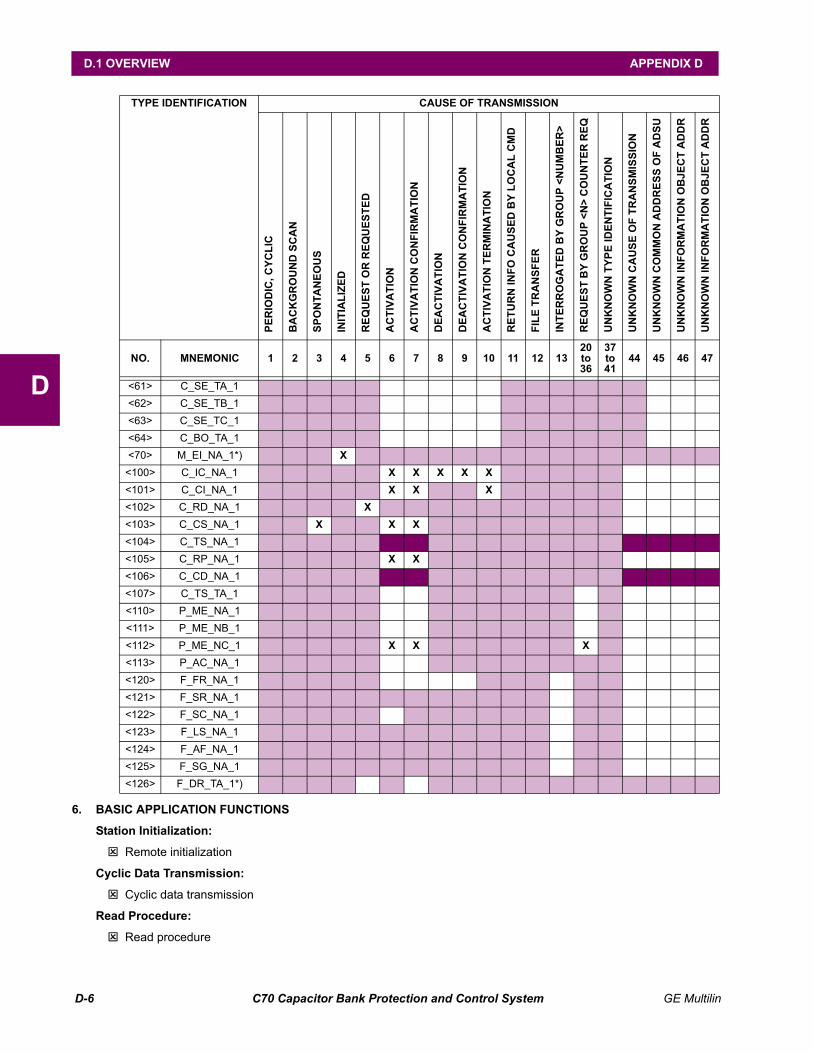
D-6 C70 Capacitor Bank Protection and Control System GE Multilin
D.1 OVERVIEW APPENDIX D
D
6. BASIC APPLICATION FUNCTIONS
Station Initialization:
Remote initialization
Cyclic Data Transmission:
Cyclic data transmission
Read Procedure:
Read procedure
<61> C_SE_TA_1
<62> C_SE_TB_1
<63> C_SE_TC_1
<64> C_BO_TA_1
<70> M_EI_NA_1*) X
<100> C_IC_NA_1 X X X X X
<101> C_CI_NA_1 X X X
<102> C_RD_NA_1 X
<103> C_CS_NA_1 X X X
<104> C_TS_NA_1
<105> C_RP_NA_1 X X
<106> C_CD_NA_1
<107> C_TS_TA_1
<110> P_ME_NA_1
<111> P_ME_NB_1
<112> P_ME_NC_1 X X X
<113> P_AC_NA_1
<120> F_FR_NA_1
<121> F_SR_NA_1
<122> F_SC_NA_1
<123> F_LS_NA_1
<124> F_AF_NA_1
<125> F_SG_NA_1
<126> F_DR_TA_1*)
TYPE IDENTIFICATION CAUSE OF TRANSMISSION
NO. MNEMONIC 1 2 3 4 5 6 7 8 9 10 11 12 1320 to 36
37 to 41
44 45 46 47
PE
RIO
DIC
, CY
CL
IC
BA
CK
GR
OU
ND
SC
AN
SP
ON
TA
NE
OU
S
INIT
IAL
IZE
D
RE
QU
ES
T O
R R
EQ
UE
ST
ED
AC
TIV
AT
ION
AC
TIV
AT
ION
CO
NF
IRM
AT
ION
DE
AC
TIV
AT
ION
DE
AC
TIV
AT
ION
CO
NF
IRM
AT
ION
AC
TIV
AT
ION
TE
RM
INA
TIO
N
RE
TU
RN
INF
O C
AU
SE
D B
Y L
OC
AL
CM
D
FIL
E T
RA
NS
FE
R
INT
ER
RO
GA
TE
D B
Y G
RO
UP
<N
UM
BE
R>
RE
QU
ES
T B
Y G
RO
UP
<N
> C
OU
NT
ER
RE
Q
UN
KN
OW
N T
YP
E ID
EN
TIF
ICA
TIO
N
UN
KN
OW
N C
AU
SE
OF
TR
AN
SM
ISS
ION
UN
KN
OW
N C
OM
MO
N A
DD
RE
SS
OF
AD
SU
UN
KN
OW
N IN
FO
RM
AT
ION
OB
JEC
T A
DD
R
UN
KN
OW
N IN
FO
RM
AT
ION
OB
JEC
T A
DD
R
GE Multilin C70 Capacitor Bank Protection and Control System D-7
APPENDIX D D.1 OVERVIEW
D
Spontaneous Transmission:
Spontaneous transmission
Double transmission of information objects with cause of transmission spontaneous:
The following type identifications may be transmitted in succession caused by a single status change of an informationobject. The particular information object addresses for which double transmission is enabled are defined in a project-specific list.
Single point information: M_SP_NA_1, M_SP_TA_1, M_SP_TB_1, and M_PS_NA_1
Double point information: M_DP_NA_1, M_DP_TA_1, and M_DP_TB_1
Step position information: M_ST_NA_1, M_ST_TA_1, and M_ST_TB_1
Bitstring of 32 bits: M_BO_NA_1, M_BO_TA_1, and M_BO_TB_1 (if defined for a specific project)
Measured value, normalized value: M_ME_NA_1, M_ME_TA_1, M_ME_ND_1, and M_ME_TD_1
Measured value, scaled value: M_ME_NB_1, M_ME_TB_1, and M_ME_TE_1
Measured value, short floating point number: M_ME_NC_1, M_ME_TC_1, and M_ME_TF_1
Station interrogation:
Clock synchronization:
Clock synchronization (optional, see Clause 7.6)
Command transmission:
Direct command transmission
Direct setpoint command transmission
Select and execute command
Select and execute setpoint command
C_SE ACTTERM used
No additional definition
Short pulse duration (duration determined by a system parameter in the outstation)
Long pulse duration (duration determined by a system parameter in the outstation)
Persistent output
Supervision of maximum delay in command direction of commands and setpoint commands
Maximum allowable delay of commands and setpoint commands: 10 s
Transmission of integrated totals:
Mode A: Local freeze with spontaneous transmission
Mode B: Local freeze with counter interrogation
Mode C: Freeze and transmit by counter-interrogation commands
Mode D: Freeze by counter-interrogation command, frozen values reported simultaneously
Counter read
Counter freeze without reset
Global
Group 1 Group 5 Group 9 Group 13
Group 2 Group 6 Group 10 Group 14
Group 3 Group 7 Group 11 Group 15
Group 4 Group 8 Group 12 Group 16
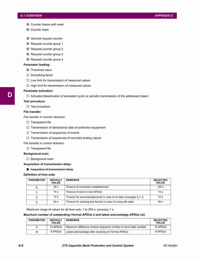
D-8 C70 Capacitor Bank Protection and Control System GE Multilin
D.1 OVERVIEW APPENDIX D
D
Counter freeze with reset
Counter reset
General request counter
Request counter group 1
Request counter group 2
Request counter group 3
Request counter group 4
Parameter loading:
Threshold value
Smoothing factor
Low limit for transmission of measured values
High limit for transmission of measured values
Parameter activation:
Activation/deactivation of persistent cyclic or periodic transmission of the addressed object
Test procedure:
Test procedure
File transfer:
File transfer in monitor direction:
Transparent file
Transmission of disturbance data of protection equipment
Transmission of sequences of events
Transmission of sequences of recorded analog values
File transfer in control direction:
Transparent file
Background scan:
Background scan
Acquisition of transmission delay:
Acquisition of transmission delay
Definition of time outs:
Maximum range of values for all time outs: 1 to 255 s, accuracy 1 s
Maximum number of outstanding I-format APDUs k and latest acknowledge APDUs (w):
PARAMETER DEFAULT VALUE
REMARKS SELECTED VALUE
t0 30 s Timeout of connection establishment 120 s
t1 15 s Timeout of send or test APDUs 15 s
t2 10 s Timeout for acknowledgements in case of no data messages t2 < t1 10 s
t3 20 s Timeout for sending test frames in case of a long idle state 20 s
PARAMETER DEFAULT VALUE
REMARKS SELECTED VALUE
k 12 APDUs Maximum difference receive sequence number to send state variable 12 APDUs
w 8 APDUs Latest acknowledge after receiving w I-format APDUs 8 APDUs
GE Multilin C70 Capacitor Bank Protection and Control System D-9
APPENDIX D D.1 OVERVIEW
D
Maximum range of values k: 1 to 32767 (215 – 1) APDUs, accuracy 1 APDU
Maximum range of values w: 1 to 32767 APDUs, accuracy 1 APDURecommendation: w should not exceed two-thirds of k.
Portnumber:
RFC 2200 suite:
RFC 2200 is an official Internet Standard which describes the state of standardization of protocols used in the Internetas determined by the Internet Architecture Board (IAB). It offers a broad spectrum of actual standards used in the Inter-net. The suitable selection of documents from RFC 2200 defined in this standard for given projects has to be chosenby the user of this standard.
Ethernet 802.3
Serial X.21 interface
Other selection(s) from RFC 2200 (list below if selected)
D.1.2 POINT LIST
The IEC 60870-5-104 data points are configured through the SETTINGS PRODUCT SETUP COMMUNICATIONS DNP /
IEC104 POINT LISTS menu. Refer to the Communications section of Chapter 5 for additional details.
PARAMETER VALUE REMARKS
Portnumber 2404 In all cases

D-10 C70 Capacitor Bank Protection and Control System GE Multilin
D.1 OVERVIEW APPENDIX D
D

GE Multilin C70 Capacitor Bank Protection and Control System E-1
APPENDIX E E.1 DEVICE PROFILE DOCUMENT
E
APPENDIX E DNP COMMUNICATIONSE.1DEVICE PROFILE DOCUMENT E.1.1 DNP V3.00 DEVICE PROFILE
The following table provides a ‘Device Profile Document’ in the standard format defined in the DNP 3.0 Subset DefinitionsDocument.
Table E–1: DNP V3.00 DEVICE PROFILE (Sheet 1 of 3)
(Also see the IMPLEMENTATION TABLE in the following section)
Vendor Name: General Electric Multilin
Device Name: UR Series Relay
Highest DNP Level Supported:
For Requests: Level 2
For Responses: Level 2
Device Function:
Master
Slave
Notable objects, functions, and/or qualifiers supported in addition to the Highest DNP Levels Supported (the completelist is described in the attached table):
Binary Inputs (Object 1)
Binary Input Changes (Object 2)
Binary Outputs (Object 10)
Control Relay Output Block (Object 12)
Binary Counters (Object 20)
Frozen Counters (Object 21)
Counter Change Event (Object 22)
Frozen Counter Event (Object 23)
Analog Inputs (Object 30)
Analog Input Changes (Object 32)
Analog Deadbands (Object 34)
Time and Date (Object 50)
File Transfer (Object 70)
Internal Indications (Object 80)
Maximum Data Link Frame Size (octets):
Transmitted: 292
Received: 292
Maximum Application Fragment Size (octets):
Transmitted: configurable up to 2048
Received: 2048
Maximum Data Link Re-tries:
None
Fixed at 3
Configurable
Maximum Application Layer Re-tries:
None
Configurable
Requires Data Link Layer Confirmation:
Never
Always
Sometimes
Configurable

E-2 C70 Capacitor Bank Protection and Control System GE Multilin
E.1 DEVICE PROFILE DOCUMENT APPENDIX E
E
Requires Application Layer Confirmation:
Never
Always
When reporting Event Data
When sending multi-fragment responses
Sometimes
Configurable
Timeouts while waiting for:
Data Link Confirm: None Fixed at ____ Variable Configurable
Complete Appl. Fragment: None Fixed at ____ Variable Configurable
Application Confirm: None Fixed at 10 s Variable Configurable
Complete Appl. Response: None Fixed at ____ Variable Configurable
Others:
Transmission Delay: No intentional delay
Need Time Interval: Configurable (default = 24 hrs.)
Select/Operate Arm Timeout: 10 s
Binary input change scanning period: 8 times per power system cycle
Analog input change scanning period: 500 ms
Counter change scanning period: 500 ms
Frozen counter event scanning period: 500 ms
Unsolicited response notification delay: 100 ms
Unsolicited response retry delay configurable 0 to 60 sec.
Sends/Executes Control Operations:
WRITE Binary Outputs Never Always Sometimes Configurable
SELECT/OPERATE Never Always Sometimes Configurable
DIRECT OPERATE Never Always Sometimes Configurable
DIRECT OPERATE – NO ACK Never Always Sometimes Configurable
Count 1 Never Always Sometimes Configurable
Pulse On Never Always Sometimes Configurable
Pulse Off Never Always Sometimes Configurable
Latch On Never Always Sometimes Configurable
Latch Off Never Always Sometimes Configurable
Queue Never Always Sometimes Configurable
Clear Queue Never Always Sometimes Configurable
Explanation of ‘Sometimes’: Object 12 points are mapped to UR Virtual Inputs. The persistence of Virtual Inputs isdetermined by the VIRTUAL INPUT X TYPE settings. Both “Pulse On” and “Latch On” operations perform the same func-tion in the UR; that is, the appropriate Virtual Input is put into the “On” state. If the Virtual Input is set to “Self-Reset”,it will reset after one pass of FlexLogic. The On/Off times and Count value are ignored. “Pulse Off” and “Latch Off”operations put the appropriate Virtual Input into the “Off” state. “Trip” and “Close” operations both put the appropriateVirtual Input into the “On” state.
Table E–1: DNP V3.00 DEVICE PROFILE (Sheet 2 of 3)

GE Multilin C70 Capacitor Bank Protection and Control System E-3
APPENDIX E E.1 DEVICE PROFILE DOCUMENT
E
Reports Binary Input Change Events when nospecific variation requested:
Never
Only time-tagged
Only non-time-tagged
Configurable
Reports time-tagged Binary Input Change Events when nospecific variation requested:
Never
Binary Input Change With Time
Binary Input Change With Relative Time
Configurable (attach explanation)
Sends Unsolicited Responses:
Never
Configurable
Only certain objects
Sometimes (attach explanation)
ENABLE/DISABLE unsolicited Function codes supported
Sends Static Data in Unsolicited Responses:
Never
When Device Restarts
When Status Flags Change
No other options are permitted.
Default Counter Object/Variation:
No Counters Reported
Configurable (attach explanation)
Default Object: 20Default Variation: 1
Point-by-point list attached
Counters Roll Over at:
No Counters Reported
Configurable (attach explanation)
16 Bits (Counter 8)
32 Bits (Counters 0 to 7, 9)
Other Value: _____
Point-by-point list attached
Sends Multi-Fragment Responses:
Yes
No
Table E–1: DNP V3.00 DEVICE PROFILE (Sheet 3 of 3)

E-4 C70 Capacitor Bank Protection and Control System GE Multilin
E.1 DEVICE PROFILE DOCUMENT APPENDIX E
E
E.1.2 IMPLEMENTATION TABLE
The following table identifies the variations, function codes, and qualifiers supported by the C70 in both request messagesand in response messages. For static (non-change-event) objects, requests sent with qualifiers 00, 01, 06, 07, or 08, will beresponded with qualifiers 00 or 01. Static object requests sent with qualifiers 17 or 28 will be responded with qualifiers 17 or28. For change-event objects, qualifiers 17 or 28 are always responded.
Table E–2: IMPLEMENTATION TABLE (Sheet 1 of 4)
OBJECT REQUEST RESPONSE
OBJECT NO.
VARIATION NO.
DESCRIPTION FUNCTION CODES (DEC)
QUALIFIER CODES (HEX)
FUNCTION CODES (DEC)
QUALIFIER CODES (HEX)
1 0 Binary Input (Variation 0 is used to request default variation)
1 (read)
22 (assign class)
00, 01 (start-stop)
06 (no range, or all)
07, 08 (limited quantity)
17, 28 (index)
1 Binary Input 1 (read)
22 (assign class)
00, 01 (start-stop)
06 (no range, or all)
07, 08 (limited quantity)
17, 28 (index)
129 (response) 00, 01 (start-stop)
17, 28 (index)
(see Note 2)
2 Binary Input with Status 1 (read)
22 (assign class)
00, 01 (start-stop)
06 (no range, or all)
07, 08 (limited quantity)
17, 28 (index)
129 (response) 00, 01 (start-stop)
17, 28 (index)
(see Note 2)
2 0 Binary Input Change (Variation 0 is used to request default variation)
1 (read) 06 (no range, or all)
07, 08 (limited quantity)
1 Binary Input Change without Time 1 (read) 06 (no range, or all)
07, 08 (limited quantity)
129 (response)
130 (unsol. resp.)
17, 28 (index)
2 Binary Input Change with Time 1 (read) 06 (no range, or all)
07, 08 (limited quantity)
129 (response
130 (unsol. resp.)
17, 28 (index)
3 Binary Input Change with Relative Time 1 (read) 06 (no range, or all)
07, 08 (limited quantity)
10 0 Binary Output Status (Variation 0 is used to request default variation)
1 (read) 00, 01(start-stop)
06 (no range, or all)
07, 08 (limited quantity)
17, 28 (index)
2 Binary Output Status 1 (read) 00, 01 (start-stop)
06 (no range, or all)
07, 08 (limited quantity)
17, 28 (index)
129 (response) 00, 01 (start-stop)
17, 28 (index)
(see Note 2)
12 1 Control Relay Output Block 3 (select)
4 (operate)
5 (direct op)
6 (dir. op, noack)
00, 01 (start-stop)
07, 08 (limited quantity)
17, 28 (index)
129 (response) echo of request
20 0 Binary Counter(Variation 0 is used to request default variation)
1 (read)
7 (freeze)
8 (freeze noack)
9 (freeze clear)
10 (frz. cl. noack)
22 (assign class)
00, 01(start-stop)
06(no range, or all)
07, 08(limited quantity)
17, 28(index)
1 32-Bit Binary Counter 1 (read)
7 (freeze)
8 (freeze noack)
9 (freeze clear)
10 (frz. cl. noack)
22 (assign class)
00, 01 (start-stop)
06 (no range, or all)
07, 08 (limited quantity)
17, 28 (index)
129 (response) 00, 01 (start-stop)
17, 28 (index)
(see Note 2)
Note 1: A default variation refers to the variation responded when variation 0 is requested and/or in class 0, 1, 2, or 3 scans. The default varia-tions for object types 1, 2, 20, 21, 22, 23, 30, and 32 are selected via relay settings. Refer to the Communications section in Chapter 5 for details. This optimizes the class 0 poll data size.
Note 2: For static (non-change-event) objects, qualifiers 17 or 28 are only responded when a request is sent with qualifiers 17 or 28, respec-tively. Otherwise, static object requests sent with qualifiers 00, 01, 06, 07, or 08, will be responded with qualifiers 00 or 01 (for change-event objects, qualifiers 17 or 28 are always responded.)
Note 3: Cold restarts are implemented the same as warm restarts – the C70 is not restarted, but the DNP process is restarted.

GE Multilin C70 Capacitor Bank Protection and Control System E-5
APPENDIX E E.1 DEVICE PROFILE DOCUMENT
E
20cont’d
2 16-Bit Binary Counter 1 (read)
7 (freeze)
8 (freeze noack)
9 (freeze clear)
10 (frz. cl. noack)
22 (assign class)
00, 01 (start-stop)
06 (no range, or all)
07, 08 (limited quantity)
17, 28 (index)
129 (response) 00, 01 (start-stop)
17, 28 (index)
(see Note 2)
5 32-Bit Binary Counter without Flag 1 (read)
7 (freeze)
8 (freeze noack)
9 (freeze clear)
10 (frz. cl. noack)
22 (assign class)
00, 01 (start-stop)
06 (no range, or all)
07, 08 (limited quantity)
17, 28 (index)
129 (response) 00, 01 (start-stop)
17, 28 (index)
(see Note 2)
6 16-Bit Binary Counter without Flag 1 (read)
7 (freeze)
8 (freeze noack)
9 (freeze clear)
10 (frz. cl. noack)
22 (assign class)
00, 01 (start-stop)
06 (no range, or all)
07, 08 (limited quantity)
17, 28 (index)
129 (response) 00, 01 (start-stop)
17, 28 (index)
(see Note 2)
21 0 Frozen Counter(Variation 0 is used to request default variation)
1 (read)
22 (assign class)
00, 01 (start-stop)
06 (no range, or all)
07, 08 (limited quantity)
17, 28 (index)
1 32-Bit Frozen Counter 1 (read)
22 (assign class)
00, 01 (start-stop)
06 (no range, or all)
07, 08 (limited quantity)
17, 28 (index)
129 (response) 00, 01 (start-stop)
17, 28 (index)
(see Note 2)
2 16-Bit Frozen Counter 1 (read)
22 (assign class)
00, 01 (start-stop)
06 (no range, or all)
07, 08 (limited quantity)
17, 28 (index)
129 (response) 00, 01 (start-stop)
17, 28 (index)
(see Note 2)
9 32-Bit Frozen Counter without Flag 1 (read)
22 (assign class)
00, 01 (start-stop)
06 (no range, or all)
07, 08 (limited quantity)
17, 28 (index)
129 (response) 00, 01 (start-stop)
17, 28 (index)
(see Note 2)
10 16-Bit Frozen Counter without Flag 1 (read)
22 (assign class)
00, 01 (start-stop)
06 (no range, or all)
07, 08 (limited quantity)
17, 28 (index)
129 (response) 00, 01 (start-stop)
17, 28 (index)
(see Note 2)
22 0 Counter Change Event (Variation 0 is used to request default variation)
1 (read) 06 (no range, or all)
07, 08 (limited quantity)
1 32-Bit Counter Change Event 1 (read) 06 (no range, or all)
07, 08 (limited quantity)
129 (response)
130 (unsol. resp.)
17, 28 (index)
2 16-Bit Counter Change Event 1 (read) 06 (no range, or all)
07, 08 (limited quantity)
129 (response)
130 (unsol. resp.)
17, 28 (index)
5 32-Bit Counter Change Event with Time 1 (read) 06 (no range, or all)
07, 08 (limited quantity)
129 (response)
130 (unsol. resp.)
17, 28 (index)
6 16-Bit Counter Change Event with Time 1 (read) 06 (no range, or all)
07, 08 (limited quantity)
129 (response)
130 (unsol. resp.)
17, 28 (index)
23 0 Frozen Counter Event (Variation 0 is used to request default variation)
1 (read) 06 (no range, or all)
07, 08 (limited quantity)
1 32-Bit Frozen Counter Event 1 (read) 06 (no range, or all)
07, 08 (limited quantity)
129 (response)
130 (unsol. resp.)
17, 28 (index)
2 16-Bit Frozen Counter Event 1 (read) 06 (no range, or all)
07, 08 (limited quantity)
129 (response)
130 (unsol. resp.)
17, 28 (index)
Table E–2: IMPLEMENTATION TABLE (Sheet 2 of 4)
OBJECT REQUEST RESPONSE
OBJECT NO.
VARIATION NO.
DESCRIPTION FUNCTION CODES (DEC)
QUALIFIER CODES (HEX)
FUNCTION CODES (DEC)
QUALIFIER CODES (HEX)
Note 1: A default variation refers to the variation responded when variation 0 is requested and/or in class 0, 1, 2, or 3 scans. The default varia-tions for object types 1, 2, 20, 21, 22, 23, 30, and 32 are selected via relay settings. Refer to the Communications section in Chapter 5 for details. This optimizes the class 0 poll data size.
Note 2: For static (non-change-event) objects, qualifiers 17 or 28 are only responded when a request is sent with qualifiers 17 or 28, respec-tively. Otherwise, static object requests sent with qualifiers 00, 01, 06, 07, or 08, will be responded with qualifiers 00 or 01 (for change-event objects, qualifiers 17 or 28 are always responded.)
Note 3: Cold restarts are implemented the same as warm restarts – the C70 is not restarted, but the DNP process is restarted.
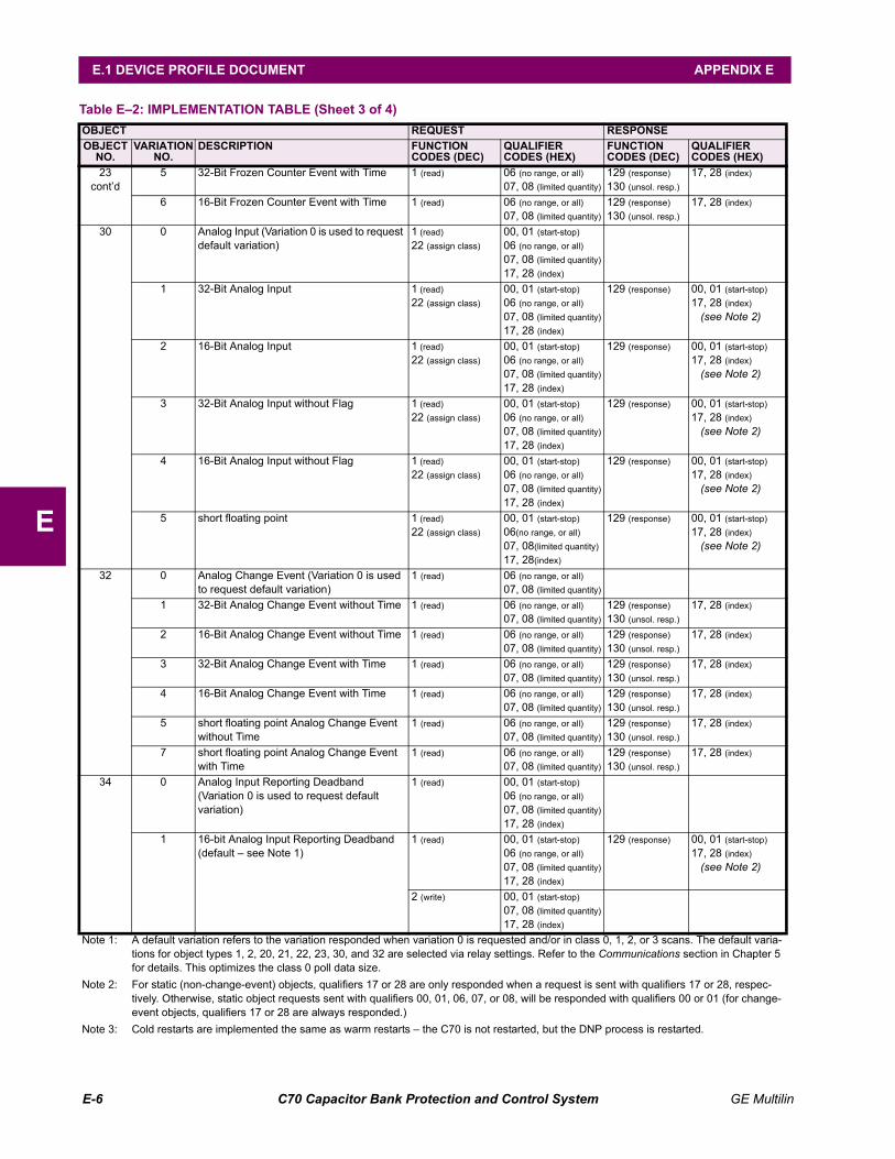
E-6 C70 Capacitor Bank Protection and Control System GE Multilin
E.1 DEVICE PROFILE DOCUMENT APPENDIX E
E
23cont’d
5 32-Bit Frozen Counter Event with Time 1 (read) 06 (no range, or all)
07, 08 (limited quantity)
129 (response)
130 (unsol. resp.)
17, 28 (index)
6 16-Bit Frozen Counter Event with Time 1 (read) 06 (no range, or all)
07, 08 (limited quantity)
129 (response)
130 (unsol. resp.)
17, 28 (index)
30 0 Analog Input (Variation 0 is used to request default variation)
1 (read)
22 (assign class)
00, 01 (start-stop)
06 (no range, or all)
07, 08 (limited quantity)
17, 28 (index)
1 32-Bit Analog Input 1 (read)
22 (assign class)
00, 01 (start-stop)
06 (no range, or all)
07, 08 (limited quantity)
17, 28 (index)
129 (response) 00, 01 (start-stop)
17, 28 (index)
(see Note 2)
2 16-Bit Analog Input 1 (read)
22 (assign class)
00, 01 (start-stop)
06 (no range, or all)
07, 08 (limited quantity)
17, 28 (index)
129 (response) 00, 01 (start-stop)
17, 28 (index)
(see Note 2)
3 32-Bit Analog Input without Flag 1 (read)
22 (assign class)
00, 01 (start-stop)
06 (no range, or all)
07, 08 (limited quantity)
17, 28 (index)
129 (response) 00, 01 (start-stop)
17, 28 (index)
(see Note 2)
4 16-Bit Analog Input without Flag 1 (read)
22 (assign class)
00, 01 (start-stop)
06 (no range, or all)
07, 08 (limited quantity)
17, 28 (index)
129 (response) 00, 01 (start-stop)
17, 28 (index)
(see Note 2)
5 short floating point 1 (read)
22 (assign class)
00, 01 (start-stop)
06(no range, or all)
07, 08(limited quantity)
17, 28(index)
129 (response) 00, 01 (start-stop)
17, 28 (index)
(see Note 2)
32 0 Analog Change Event (Variation 0 is used to request default variation)
1 (read) 06 (no range, or all)
07, 08 (limited quantity)
1 32-Bit Analog Change Event without Time 1 (read) 06 (no range, or all)
07, 08 (limited quantity)
129 (response)
130 (unsol. resp.)
17, 28 (index)
2 16-Bit Analog Change Event without Time 1 (read) 06 (no range, or all)
07, 08 (limited quantity)
129 (response)
130 (unsol. resp.)
17, 28 (index)
3 32-Bit Analog Change Event with Time 1 (read) 06 (no range, or all)
07, 08 (limited quantity)
129 (response)
130 (unsol. resp.)
17, 28 (index)
4 16-Bit Analog Change Event with Time 1 (read) 06 (no range, or all)
07, 08 (limited quantity)
129 (response)
130 (unsol. resp.)
17, 28 (index)
5 short floating point Analog Change Event without Time
1 (read) 06 (no range, or all)
07, 08 (limited quantity)
129 (response)
130 (unsol. resp.)
17, 28 (index)
7 short floating point Analog Change Event with Time
1 (read) 06 (no range, or all)
07, 08 (limited quantity)
129 (response)
130 (unsol. resp.)
17, 28 (index)
34 0 Analog Input Reporting Deadband(Variation 0 is used to request default variation)
1 (read) 00, 01 (start-stop)
06 (no range, or all)
07, 08 (limited quantity)
17, 28 (index)
1 16-bit Analog Input Reporting Deadband(default – see Note 1)
1 (read) 00, 01 (start-stop)
06 (no range, or all)
07, 08 (limited quantity)
17, 28 (index)
129 (response) 00, 01 (start-stop)
17, 28 (index)
(see Note 2)
2 (write) 00, 01 (start-stop)
07, 08 (limited quantity)
17, 28 (index)
Table E–2: IMPLEMENTATION TABLE (Sheet 3 of 4)
OBJECT REQUEST RESPONSE
OBJECT NO.
VARIATION NO.
DESCRIPTION FUNCTION CODES (DEC)
QUALIFIER CODES (HEX)
FUNCTION CODES (DEC)
QUALIFIER CODES (HEX)
Note 1: A default variation refers to the variation responded when variation 0 is requested and/or in class 0, 1, 2, or 3 scans. The default varia-tions for object types 1, 2, 20, 21, 22, 23, 30, and 32 are selected via relay settings. Refer to the Communications section in Chapter 5 for details. This optimizes the class 0 poll data size.
Note 2: For static (non-change-event) objects, qualifiers 17 or 28 are only responded when a request is sent with qualifiers 17 or 28, respec-tively. Otherwise, static object requests sent with qualifiers 00, 01, 06, 07, or 08, will be responded with qualifiers 00 or 01 (for change-event objects, qualifiers 17 or 28 are always responded.)
Note 3: Cold restarts are implemented the same as warm restarts – the C70 is not restarted, but the DNP process is restarted.

GE Multilin C70 Capacitor Bank Protection and Control System E-7
APPENDIX E E.1 DEVICE PROFILE DOCUMENT
E
34cont’d
2 32-bit Analog Input Reporting Deadband 1 (read) 00, 01 (start-stop)
06 (no range, or all)
07, 08 (limited quantity)
17, 28 (index)
129 (response) 00, 01 (start-stop)
17, 28 (index)
(see Note 2)
2 (write) 00, 01 (start-stop)
07, 08 (limited quantity)
17, 28 (index)
3 Short floating point Analog Input Reporting Deadband
1 (read) 00, 01 (start-stop)
06 (no range, or all)
07, 08 (limited quantity)
17, 28 (index)
129 (response) 00, 01 (start-stop)
17, 28 (index)
(see Note 2)
50 1 Time and Date(default – see Note 1)
1 (read)
2 (write)
00, 01 (start-stop)
06 (no range, or all)
07 (limited qty=1)
08 (limited quantity)
17, 28 (index)
129 (response) 00, 01 (start-stop)
17, 28 (index)
(see Note 2)
52 2 Time Delay Fine 129 (response) 07 (limited quantity)
(quantity = 1)
60 0 Class 0, 1, 2, and 3 Data 1 (read)
20 (enable unsol)
21 (disable unsol)
22 (assign class)
06 (no range, or all)
1 Class 0 Data 1 (read)
22 (assign class)
06 (no range, or all)
2 Class 1 Data 1 (read)
20 (enable unsol)
21 (disable unsol)
22 (assign class)
06 (no range, or all)
07, 08 (limited quantity)3 Class 2 Data
4 Class 3 Data
70 0 File event - any variation 1 (read) 06 (no range, or all)
07, 08 (limited quantity)
22 (assign class) 06 (no range, or all)
2 File authentication 29 (authenticate) 5b (free format) 129 (response) 5b (free format)
3 File command 25 (open)
27 (delete)
5b (free format)
4 File command status 26 (close)
30 (abort)
5b (free format) 129 (response)
130 (unsol. resp.)
5b (free format)
5 File transfer 1 (read)
2 (write)
5b (free format) 129 (response)
130 (unsol. resp.)
5b (free format)
6 File transfer status 129 (response)
130 (unsol. resp.)
5b (free format)
7 File descriptor 28 (get file info.) 5b (free format) 129 (response)
130 (unsol. resp.)
5b (free format)
80 1 Internal Indications 1 (read) 00, 01 (start-stop)
(index =7)129 (response) 00, 01 (start-stop)
2 (write)
(see Note 3)00 (start-stop)
(index =7)
--- No Object (function code only)see Note 3
13 (cold restart)
--- No Object (function code only) 14 (warm restart)
--- No Object (function code only) 23 (delay meas.)
Table E–2: IMPLEMENTATION TABLE (Sheet 4 of 4)
OBJECT REQUEST RESPONSE
OBJECT NO.
VARIATION NO.
DESCRIPTION FUNCTION CODES (DEC)
QUALIFIER CODES (HEX)
FUNCTION CODES (DEC)
QUALIFIER CODES (HEX)
Note 1: A default variation refers to the variation responded when variation 0 is requested and/or in class 0, 1, 2, or 3 scans. The default varia-tions for object types 1, 2, 20, 21, 22, 23, 30, and 32 are selected via relay settings. Refer to the Communications section in Chapter 5 for details. This optimizes the class 0 poll data size.
Note 2: For static (non-change-event) objects, qualifiers 17 or 28 are only responded when a request is sent with qualifiers 17 or 28, respec-tively. Otherwise, static object requests sent with qualifiers 00, 01, 06, 07, or 08, will be responded with qualifiers 00 or 01 (for change-event objects, qualifiers 17 or 28 are always responded.)
Note 3: Cold restarts are implemented the same as warm restarts – the C70 is not restarted, but the DNP process is restarted.
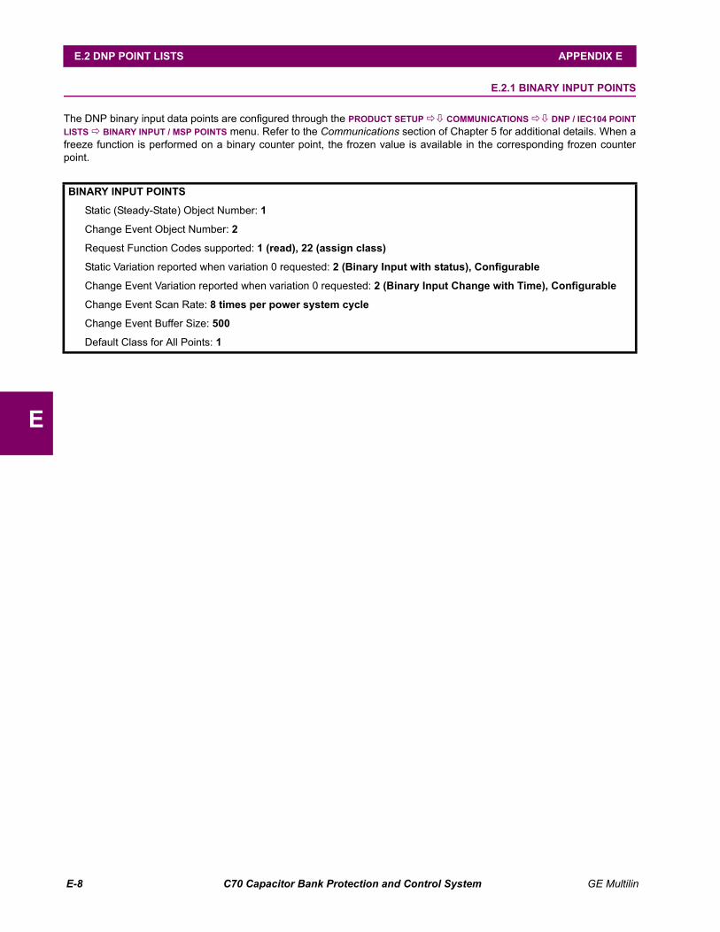
E-8 C70 Capacitor Bank Protection and Control System GE Multilin
E.2 DNP POINT LISTS APPENDIX E
E
E.2DNP POINT LISTS E.2.1 BINARY INPUT POINTS
The DNP binary input data points are configured through the PRODUCT SETUP COMMUNICATIONS DNP / IEC104 POINT
LISTS BINARY INPUT / MSP POINTS menu. Refer to the Communications section of Chapter 5 for additional details. When afreeze function is performed on a binary counter point, the frozen value is available in the corresponding frozen counterpoint.
BINARY INPUT POINTS
Static (Steady-State) Object Number: 1
Change Event Object Number: 2
Request Function Codes supported: 1 (read), 22 (assign class)
Static Variation reported when variation 0 requested: 2 (Binary Input with status), Configurable
Change Event Variation reported when variation 0 requested: 2 (Binary Input Change with Time), Configurable
Change Event Scan Rate: 8 times per power system cycle
Change Event Buffer Size: 500
Default Class for All Points: 1
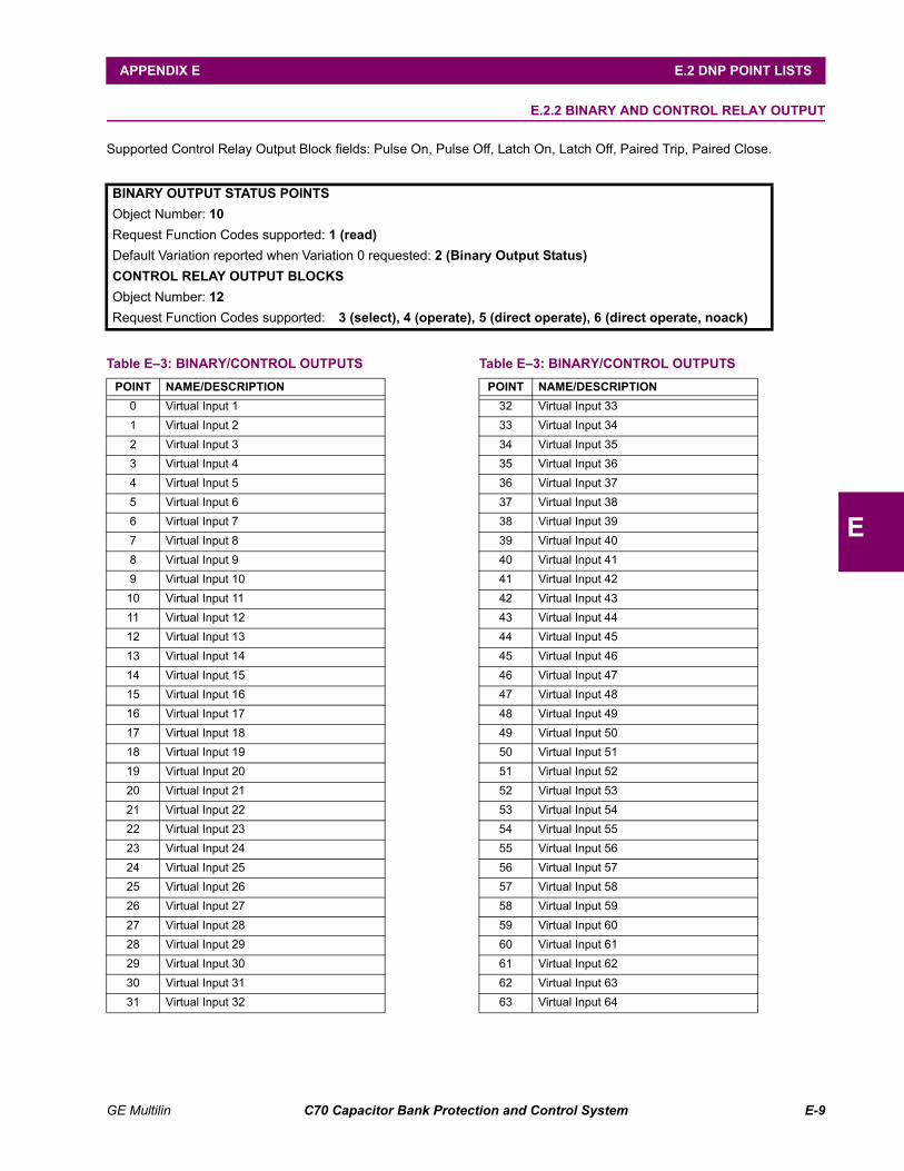
GE Multilin C70 Capacitor Bank Protection and Control System E-9
APPENDIX E E.2 DNP POINT LISTS
E
E.2.2 BINARY AND CONTROL RELAY OUTPUT
Supported Control Relay Output Block fields: Pulse On, Pulse Off, Latch On, Latch Off, Paired Trip, Paired Close.
BINARY OUTPUT STATUS POINTS
Object Number: 10
Request Function Codes supported: 1 (read)
Default Variation reported when Variation 0 requested: 2 (Binary Output Status)
CONTROL RELAY OUTPUT BLOCKS
Object Number: 12
Request Function Codes supported: 3 (select), 4 (operate), 5 (direct operate), 6 (direct operate, noack)
Table E–3: BINARY/CONTROL OUTPUTS
POINT NAME/DESCRIPTION
0 Virtual Input 1
1 Virtual Input 2
2 Virtual Input 3
3 Virtual Input 4
4 Virtual Input 5
5 Virtual Input 6
6 Virtual Input 7
7 Virtual Input 8
8 Virtual Input 9
9 Virtual Input 10
10 Virtual Input 11
11 Virtual Input 12
12 Virtual Input 13
13 Virtual Input 14
14 Virtual Input 15
15 Virtual Input 16
16 Virtual Input 17
17 Virtual Input 18
18 Virtual Input 19
19 Virtual Input 20
20 Virtual Input 21
21 Virtual Input 22
22 Virtual Input 23
23 Virtual Input 24
24 Virtual Input 25
25 Virtual Input 26
26 Virtual Input 27
27 Virtual Input 28
28 Virtual Input 29
29 Virtual Input 30
30 Virtual Input 31
31 Virtual Input 32
32 Virtual Input 33
33 Virtual Input 34
34 Virtual Input 35
35 Virtual Input 36
36 Virtual Input 37
37 Virtual Input 38
38 Virtual Input 39
39 Virtual Input 40
40 Virtual Input 41
41 Virtual Input 42
42 Virtual Input 43
43 Virtual Input 44
44 Virtual Input 45
45 Virtual Input 46
46 Virtual Input 47
47 Virtual Input 48
48 Virtual Input 49
49 Virtual Input 50
50 Virtual Input 51
51 Virtual Input 52
52 Virtual Input 53
53 Virtual Input 54
54 Virtual Input 55
55 Virtual Input 56
56 Virtual Input 57
57 Virtual Input 58
58 Virtual Input 59
59 Virtual Input 60
60 Virtual Input 61
61 Virtual Input 62
62 Virtual Input 63
63 Virtual Input 64
Table E–3: BINARY/CONTROL OUTPUTS
POINT NAME/DESCRIPTION

E-10 C70 Capacitor Bank Protection and Control System GE Multilin
E.2 DNP POINT LISTS APPENDIX E
E
E.2.3 COUNTERS
The following table lists both Binary Counters (Object 20) and Frozen Counters (Object 21). When a freeze function is per-formed on a Binary Counter point, the frozen value is available in the corresponding Frozen Counter point.
A counter freeze command has no meaning for counters 8 and 9. C70 Digital Counter values are represented as 32-bitintegers. The DNP 3.0 protocol defines counters to be unsigned integers. Care should be taken when interpreting negativecounter values.
BINARY COUNTERS
Static (Steady-State) Object Number: 20
Change Event Object Number: 22
Request Function Codes supported: 1 (read), 7 (freeze), 8 (freeze noack), 9 (freeze and clear),10 (freeze and clear, noack), 22 (assign class)
Static Variation reported when variation 0 requested: 1 (32-Bit Binary Counter with Flag)
Change Event Variation reported when variation 0 requested: 1 (32-Bit Counter Change Event without time)
Change Event Buffer Size: 10
Default Class for all points: 3
FROZEN COUNTERS
Static (Steady-State) Object Number: 21
Change Event Object Number: 23
Request Function Codes supported: 1 (read)
Static Variation reported when variation 0 requested: 1 (32-Bit Frozen Counter with Flag)
Change Event Variation reported when variation 0 requested: 1 (32-Bit Frozen Counter Event without time)
Change Event Buffer Size: 10
Default Class for all points: 3
Table E–4: BINARY AND FROZEN COUNTERS
POINTINDEX
NAME/DESCRIPTION
0 Digital Counter 1
1 Digital Counter 2
2 Digital Counter 3
3 Digital Counter 4
4 Digital Counter 5
5 Digital Counter 6
6 Digital Counter 7
7 Digital Counter 8
8 Oscillography Trigger Count
9 Events Since Last Clear
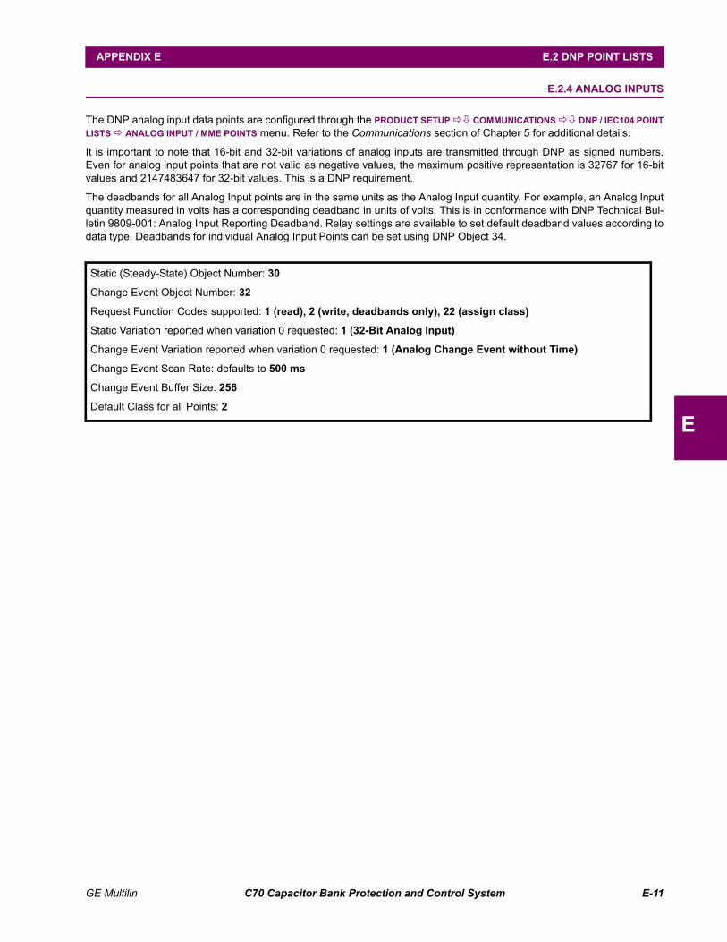
GE Multilin C70 Capacitor Bank Protection and Control System E-11
APPENDIX E E.2 DNP POINT LISTS
E
E.2.4 ANALOG INPUTS
The DNP analog input data points are configured through the PRODUCT SETUP COMMUNICATIONS DNP / IEC104 POINT
LISTS ANALOG INPUT / MME POINTS menu. Refer to the Communications section of Chapter 5 for additional details.
It is important to note that 16-bit and 32-bit variations of analog inputs are transmitted through DNP as signed numbers.Even for analog input points that are not valid as negative values, the maximum positive representation is 32767 for 16-bitvalues and 2147483647 for 32-bit values. This is a DNP requirement.
The deadbands for all Analog Input points are in the same units as the Analog Input quantity. For example, an Analog Inputquantity measured in volts has a corresponding deadband in units of volts. This is in conformance with DNP Technical Bul-letin 9809-001: Analog Input Reporting Deadband. Relay settings are available to set default deadband values according todata type. Deadbands for individual Analog Input Points can be set using DNP Object 34.
Static (Steady-State) Object Number: 30
Change Event Object Number: 32
Request Function Codes supported: 1 (read), 2 (write, deadbands only), 22 (assign class)
Static Variation reported when variation 0 requested: 1 (32-Bit Analog Input)
Change Event Variation reported when variation 0 requested: 1 (Analog Change Event without Time)
Change Event Scan Rate: defaults to 500 ms
Change Event Buffer Size: 256
Default Class for all Points: 2

E-12 C70 Capacitor Bank Protection and Control System GE Multilin
E.2 DNP POINT LISTS APPENDIX E
E

GE Multilin C70 Capacitor Bank Protection and Control System F-1
APPENDIX F F.1 CHANGE NOTES
F
APPENDIX F MISCELLANEOUSF.1CHANGE NOTES F.1.1 REVISION HISTORY
F.1.2 CHANGES TO THE C70 MANUAL
Table F–1: REVISION HISTORY
MANUAL P/N C70 REVISION RELEASE DATE ECO
1601-9015-P1 5.2x 23 October 2006 URX-230
1601-9015-P2 5.2x 24 January 2007 URX-232
1601-9015-R1 5.4x 26 June 2007 URX-242
1601-9015-R2 5.4x 31 August 2007 URX-246
1601-9015-R3 5.4x 17 October 2007 URX-251
1601-9015-S1 5.5x 7 December 2007 URX-253
1601-9015-S2 5.5x 22 February 2008 URX-258
1601-9015-S3 5.5x 12 March 2008 URX-260
1601-9015-T1 5.6x 27 June 2008 08-0390
1601-9015-U1 5.7x 29 May 2009 09-0938
1601-9015-U2 5.7x 30 September 2009 09-1165
1601-9015-V1 5.8x 29 May 2010 09-1457
1601-9015-V2 5.8x 04 January 2011 11-2237
1601-9015-W1 5.9x 12 January 2011 11-2227
1601-9015-X1 6.0x 21 December 2011 11-2840
1601-9015-X2 6.0x 5 April 2012 12-3254
1601-9015-Y1 7.0x 30 September 2012 12-3529
1601-9015-Y2 7.0x 11 November 2012 12-3601
1601-9015-Y3 7.0x 30 April 2013 13-0167
Table F–2: MAJOR UPDATES FOR C70 MANUAL REVISION Y3
PAGE (Y2)
PAGE (Y3)
CHANGE DESCRIPTION
-- xi Add Added battery disposal information as chapter 0
1-1 1-1 Add Added General Cautions and Warnings to section 1.1.1
2 2 Update Updated several specifications
5-228 5-228 Add Reinserted section 5.8.5c Remote Devices: ID of Device for Receiving GSSE/GOOSE Messages, meaning the Settings > Input/Outputs > Remote Devices settings
Table F–3: MAJOR UPDATES FOR C70 MANUAL REVISION Y2
PAGE (Y1)
PAGE (Y2)
CHANGE DESCRIPTION
All All Update Minor changes throughout document
All All Delete Deleted CPU options U and V
1-1 1-1 Update Updated Figure 1-1 Rear Nameplate
3-8 3-8 Update Updated Figure 3-10 Rear Terminal View
Table F–4: MAJOR UPDATES FOR C70 MANUAL REVISION Y1 (Sheet 1 of 3)
PAGE (X2)
PAGE (Y1)
CHANGE DESCRIPTION
All All Delete Deleted content pertaining to Ethernet switch

F-2 C70 Capacitor Bank Protection and Control System GE Multilin
F.1 CHANGE NOTES APPENDIX F
F
Title Title Update Changed part numbers. Updated address and contact information.
1-1 1-1 Update Updated address and contact information
2-4 2-4 Update Updated order code Tables 2-3 to 2-6
2-8 2-8 Delete Deleted 9S, 2S, 2T from replacement module order codes Tables 2-7 and 2-8
2-18 2-18 Update Updated Ethernet fiber table in section 2.2.8 Communications
3-8 3-8 Update Updated Figure 3-10 Rear Terminal View
3-9 3-9 Update Updated Figure 3-12 Typical Wiring Diagram
3-22 3-22 Update Deleted references to COM 1 RS485 port in section 3.2.9 CPU Communication Ports. Revised text and Figure 3-24 CPU Module Communications Wiring to include only modules T, U, V in section 3.2.9a.
5-1 5-1 Update Updated the front panel main menu to include the CyberSentry security menu
5-15 5-15 Update Updated Communications main menu to remove the SNTP Protocol submenu
5-15 5-15 Delete Deleted references to COM 1 RS485 port in section 5.2.4b Serial Ports
5-16 5-16 Add Added section 5.2.4c Ethernet Network Topology
5-16 5-16 Update Updated Networks section 5.2.4d to include all three Ethernet ports
5-16 5-16 Update Added 0 as valid number to section 5.2.4e Modbus Protocol section
5-39 5- Delete Deleted Local Time Offset, Daylight Savings Time, DST (start/stop for month/day/hour) from Real Time Clock menu
5- 5-39 Add Added submenus Precision Time Protocol, SNTP Protocol, and Local Time and Synchronizing Source settings to Real Time Clock menu
5- 5-40 Add Added new Precision Time Protocol (1588) menu and setting descriptions
5- 5- Update Updated Communication to Real Time Clock in SNTP protocol settings path. Moved SNTP Protocol menu and settings descriptions to Real Time Clock subsection
5-36 5- Delete Deleted section k) SNTP Protocol and the settings descriptions
5- 5-43 Add Added new section for Local Time menu settings and settings description
5- 5-52 Add Added new PTP Fail menu item to the User-Programmable Self Tests menu
5- 5- Add Added PTP Failure and CLOCK UNSYNCHRONIZED to FlexLogic Operands table
5- 5-112 Update Added row for DeltaTime to Table 5-: FlexElement Base Units
5-146 5-150 Update Updated Figure 5-64 Neutral Current Unbalance Scheme Logic (went from A2 to A1_2 file)
5-223 5-223 Delete Deleted section 5.8.5c Remote Devices: ID of Device for Receiving GSSE/GOOSE Messages, meaning the Settings > Input/Outputs > Remote Devices settings
5- 5-238 Add Added new CyberSentry security section and main menu, local passwords, session settings, restore defaults, and supervisory subsections to Chapter 5
6-1 6-1 Update Update Actual Values main menu to include Real Time Clock Synchronization submenu
6- 6-7 Add Added new section for Real Time Clock synchronizing consisting of the menu of settings and the setting descriptions
6-9 6-9 Delete Deleted section 6.2.17 Ethernet Switch
6- 6-10 Add Added new section 6.2.18 Remaining Connection Status
7- 7-1 Add Added Security command to the Commands main menu
7- 7-3 Add Added Reboot Relay command and description to the Relay Maintenance menu items
7- 7- Add Added Security menu and submenu commands and descriptions to the Command menu
7- 7- Add Added to Minor self-test error message **Bad PTP Signal**
8- 8-4 Add Added new section for CyberSentry software option with overview and security menu subsections
A- A- Add Added FlexAnalog item PTP–IRIG-B Delta to Table A-1: FlexAnalog Data Items
B-8 B-8 Update Updated Modbus memory map table to include port 0 for Modbus slave address, TCP, DNP, HTTP, TFTP, MMS, and removed references to COM 1 RS485 port
Table F–4: MAJOR UPDATES FOR C70 MANUAL REVISION Y1 (Sheet 2 of 3)
PAGE (X2)
PAGE (Y1)
CHANGE DESCRIPTION

GE Multilin C70 Capacitor Bank Protection and Control System F-3
APPENDIX F F.1 CHANGE NOTES
F
C-23 C-23 Update Updated tables in sections C.6.3 ACSI Services Conformance Statement and C.7.1 Logical Nodes Table
Table F–4: MAJOR UPDATES FOR C70 MANUAL REVISION Y1 (Sheet 3 of 3)
PAGE (X2)
PAGE (Y1)
CHANGE DESCRIPTION

F-4 C70 Capacitor Bank Protection and Control System GE Multilin
F.2 ABBREVIATIONS APPENDIX F
F
F.2ABBREVIATIONS F.2.1 STANDARD ABBREVIATIONS
A..................... AmpereAC .................. Alternating CurrentA/D ................. Analog to DigitalAE .................. Accidental Energization, Application EntityAMP ............... AmpereANG ............... AngleANSI............... American National Standards InstituteAR .................. Automatic ReclosureASDU ............. Application-layer Service Data UnitASYM ............. AsymmetryAUTO ............. AutomaticAUX................ AuxiliaryAVG................ Average
BER................ Bit Error RateBF................... Breaker FailBFI.................. Breaker Failure InitiateBKR................ BreakerBLK ................ BlockBLKG.............. BlockingBPNT.............. Breakpoint of a characteristicBRKR ............. Breaker
CAP................ CapacitorCC .................. Coupling CapacitorCCVT ............. Coupling Capacitor Voltage TransformerCFG................ Configure / Configurable.CFG............... Filename extension for oscillography filesCHK................ CheckCHNL ............. ChannelCLS ................ CloseCLSD.............. ClosedCMND ............ CommandCMPRSN........ ComparisonCO.................. Contact OutputCOM............... CommunicationCOMM............ CommunicationsCOMP ............ Compensated, ComparisonCONN............. ConnectionCONT ............. Continuous, ContactCO-ORD......... CoordinationCPU................ Central Processing UnitCRC ............... Cyclic Redundancy CodeCRT, CRNT .... CurrentCSA................ Canadian Standards AssociationCT .................. Current TransformerCVT ................ Capacitive Voltage Transformer
D/A ................. Digital to AnalogDC (dc)........... Direct CurrentDD .................. Disturbance DetectorDFLT .............. DefaultDGNST........... DiagnosticsDI.................... Digital InputDIFF ............... DifferentialDIR ................. DirectionalDISCREP ....... DiscrepancyDIST ............... DistanceDMD ............... DemandDNP................ Distributed Network ProtocolDPO ............... DropoutDSP................ Digital Signal Processordt .................... Rate of ChangeDTT ................ Direct Transfer TripDUTT.............. Direct Under-reaching Transfer Trip
ENCRMNT ..... EncroachmentEPRI............... Electric Power Research Institute.EVT ............... Filename extension for event recorder filesEXT ................ Extension, External
F ..................... FieldFAIL................ FailureFD .................. Fault DetectorFDH................ Fault Detector high-setFDL ................ Fault Detector low-setFLA................. Full Load CurrentFO .................. Fiber Optic
FREQ............. FrequencyFSK................ Frequency-Shift KeyingFTP ................ File Transfer ProtocolFxE ................ FlexElement™FWD............... Forward
G .................... GeneratorGE.................. General ElectricGND............... GroundGNTR............. GeneratorGOOSE.......... General Object Oriented Substation EventGPS ............... Global Positioning System
HARM ............ Harmonic / HarmonicsHCT ............... High Current TimeHGF ............... High-Impedance Ground Fault (CT)HIZ ................. High-Impedance and Arcing GroundHMI ................ Human-Machine InterfaceHTTP ............. Hyper Text Transfer ProtocolHYB ............... Hybrid
I...................... InstantaneousI_0.................. Zero Sequence currentI_1.................. Positive Sequence currentI_2.................. Negative Sequence currentIA ................... Phase A currentIAB ................. Phase A minus B currentIB ................... Phase B currentIBC................. Phase B minus C currentIC ................... Phase C currentICA................. Phase C minus A currentID ................... IdentificationIED................. Intelligent Electronic DeviceIEC................. International Electrotechnical CommissionIEEE............... Institute of Electrical and Electronic EngineersIG ................... Ground (not residual) currentIgd.................. Differential Ground currentIN ................... CT Residual Current (3Io) or InputINC SEQ ........ Incomplete SequenceINIT ................ InitiateINST............... InstantaneousINV................. InverseI/O .................. Input/OutputIOC ................ Instantaneous OvercurrentIOV................. Instantaneous OvervoltageIRIG ............... Inter-Range Instrumentation GroupISO................. International Standards OrganizationIUV................. Instantaneous Undervoltage
K0 .................. Zero Sequence Current CompensationkA................... kiloAmperekV................... kiloVolt
LED................ Light Emitting DiodeLEO................ Line End OpenLFT BLD ........ Left BlinderLOOP............. LoopbackLPU................ Line PickupLRA................ Locked-Rotor CurrentLTC ................ Load Tap-Changer
M.................... MachinemA ................. MilliAmpereMAG............... MagnitudeMAN............... Manual / ManuallyMAX ............... MaximumMIC ................ Model Implementation ConformanceMIN ................ Minimum, MinutesMMI................ Man Machine InterfaceMMS .............. Manufacturing Message SpecificationMRT ............... Minimum Response TimeMSG............... MessageMTA................ Maximum Torque AngleMTR ............... MotorMVA ............... MegaVolt-Ampere (total 3-phase)MVA_A........... MegaVolt-Ampere (phase A)MVA_B........... MegaVolt-Ampere (phase B)MVA_C........... MegaVolt-Ampere (phase C)

GE Multilin C70 Capacitor Bank Protection and Control System F-5
APPENDIX F F.2 ABBREVIATIONS
F
MVAR............. MegaVar (total 3-phase)MVAR_A......... MegaVar (phase A)MVAR_B......... MegaVar (phase B)MVAR_C ........ MegaVar (phase C)MVARH .......... MegaVar-HourMW................. MegaWatt (total 3-phase)MW_A ............ MegaWatt (phase A)MW_B ............ MegaWatt (phase B)MW_C ............ MegaWatt (phase C)MWH .............. MegaWatt-Hour
N..................... NeutralN/A, n/a .......... Not ApplicableNEG ............... NegativeNMPLT ........... NameplateNOM............... NominalNTR................ Neutral
O .................... OverOC, O/C ......... OvercurrentO/P, Op........... OutputOP.................. OperateOPER............. OperateOPERATG...... OperatingO/S................. Operating SystemOSI ................. Open Systems InterconnectOSB................ Out-of-Step BlockingOUT................ OutputOV.................. OvervoltageOVERFREQ... OverfrequencyOVLD ............. Overload
P..................... PhasePC .................. Phase Comparison, Personal ComputerPCNT ............. PercentPF................... Power Factor (total 3-phase)PF_A .............. Power Factor (phase A)PF_B .............. Power Factor (phase B)PF_C.............. Power Factor (phase C)PFLL............... Phase and Frequency Lock LoopPHS................ PhasePICS............... Protocol Implementation & Conformance StatementPKP................ PickupPLC ................ Power Line CarrierPOS................ PositivePOTT.............. Permissive Over-reaching Transfer TripPRESS........... PressurePRI ................. PrimaryPROT ............. ProtectionPSEL.............. Presentation Selectorpu ................... Per UnitPUIB............... Pickup Current BlockPUIT............... Pickup Current TripPUSHBTN...... PushbuttonPUTT.............. Permissive Under-reaching Transfer TripPWM .............. Pulse Width ModulatedPWR............... Power
QUAD............. Quadrilateral
R..................... Rate, ReverseRCA................ Reach Characteristic AngleREF................ ReferenceREM ............... RemoteREV................ ReverseRI.................... Reclose InitiateRIP ................. Reclose In ProgressRGT BLD........ Right BlinderROD ............... Remote Open DetectorRST................ ResetRSTR ............. RestrainedRTD................ Resistance Temperature DetectorRTU................ Remote Terminal UnitRX (Rx) .......... Receive, Receiver
s ..................... secondS..................... SensitiveSAT ................ CT SaturationSBO................ Select Before OperateSCADA........... Supervisory Control and Data AcquisitionSEC................ Secondary

F-6 C70 Capacitor Bank Protection and Control System GE Multilin
F.2 ABBREVIATIONS APPENDIX F
F
SEL ................ Select / Selector / SelectionSENS ............. SensitiveSEQ................ SequenceSIR ................. Source Impedance RatioSNTP.............. Simple Network Time ProtocolSRC................ SourceSSB................ Single Side BandSSEL .............. Session SelectorSTATS ............ StatisticsSUPN ............. SupervisionSUPV ............. Supervise / SupervisionSV .................. Supervision, ServiceSYNC ............. SynchrocheckSYNCHCHK ... Synchrocheck
T ..................... Time, transformerTC .................. Thermal CapacityTCP ................ Transmission Control ProtocolTCU................ Thermal Capacity UsedTD MULT........ Time Dial MultiplierTEMP ............. TemperatureTFTP .............. Trivial File Transfer ProtocolTHD................ Total Harmonic DistortionTMR ............... TimerTOC................ Time OvercurrentTOV................ Time OvervoltageTRANS ........... TransientTRANSF......... TransferTSEL .............. Transport SelectorTUC................ Time UndercurrentTUV ................ Time UndervoltageTX (Tx) ........... Transmit, Transmitter
U..................... UnderUC .................. UndercurrentUCA................ Utility Communications ArchitectureUDP................ User Datagram ProtocolUL................... Underwriters LaboratoriesUNBAL ........... UnbalanceUR .................. Universal RelayURC ............... Universal Recloser Control.URS............... Filename extension for settings filesUV .................. Undervoltage
V/Hz ............... Volts per HertzV_0................. Zero Sequence voltageV_1................. Positive Sequence voltageV_2................. Negative Sequence voltageVA................... Phase A voltageVAB ................ Phase A to B voltageVAG................ Phase A to Ground voltageVARH ............. Var-hour voltageVB .................. Phase B voltageVBA................ Phase B to A voltageVBG................ Phase B to Ground voltageVC .................. Phase C voltageVCA................ Phase C to A voltageVCG ............... Phase C to Ground voltageVF................... Variable FrequencyVIBR............... VibrationVT................... Voltage TransformerVTFF .............. Voltage Transformer Fuse FailureVTLOS ........... Voltage Transformer Loss Of Signal
WDG .............. WindingWH ................. Watt-hourw/ opt.............. With OptionWRT ............... With Respect To
X..................... ReactanceXDUCER ........ TransducerXFMR ............. Transformer
Z ..................... Impedance, Zone

GE Multilin C70 Capacitor Bank Protection and Control System F-7
APPENDIX F F.3 WARRANTY
F
F.3WARRANTY F.3.1 GE MULTILIN WARRANTY
GE MULTILIN RELAY WARRANTY
GE Multilin warrants each relay it manufactures to be free from defects in material and workman-ship under normal use and service for a period of 24 months from date of shipment from factory.
In the event of a failure covered by warranty, GE Multilin will undertake to repair or replace the relayproviding the warrantor determined that it is defective and it is returned with all transportationcharges prepaid to an authorized service centre or the factory. Repairs or replacement under war-ranty will be made without charge.
Warranty shall not apply to any relay which has been subject to misuse, negligence, accident,incorrect installation or use not in accordance with instructions nor any unit that has been alteredoutside a GE Multilin authorized factory outlet.
GE Multilin is not liable for special, indirect or consequential damages or for loss of profit or forexpenses sustained as a result of a relay malfunction, incorrect application or adjustment.
For complete text of Warranty (including limitations and disclaimers), refer to GE Multilin StandardConditions of Sale.

F-8 C70 Capacitor Bank Protection and Control System GE Multilin
F.3 WARRANTY APPENDIX F
F

GE Multilin C70 Capacitor Bank Protection and Control System i
INDEX
Numerics
10BASE-Fsettings .................................................................5-24, 5-25
A
ABBREVIATIONS............................................................... F-4AC CURRENT INPUTS ................................... 2-13, 3-11, 5-80AC VOLTAGE INPUTS .............................................2-13, 3-12ACTIVATING THE RELAY ........................................1-18, 4-27ACTIVE SETTING GROUP ............................................. 5-122ACTUAL VALUES
metering........................................................................ 6-10product information ........................................................ 6-23status .............................................................................. 6-3
ALARM LEDs ................................................................... 5-59ANSI DEVICE NUMBERS ................................................... 2-2APPARENT POWER ................................................2-13, 6-15APPLICATION EXAMPLES
breaker trip circuit integrity .......................................... 5-207contact inputs .............................................................. 5-223
APPROVALS ................................................................... 2-19ARCHITECTURE ........................................................... 5-100AUTOMATIC VOLTAGE REGULATOR
FlexLogic operands ..................................................... 5-102Modbus registers ........................................................... B-45settings ....................................................................... 5-200specifications .................................................................. 2-8
AUXILIARY OVERVOLTAGEFlexLogic operands ..................................................... 5-102logic ............................................................................ 5-172Modbus registers ........................................................... B-39settings ....................................................................... 5-172specifications ................................................................ 2-10
AUXILIARY VOLTAGE CHANNEL ..................................... 3-12AUXILIARY VOLTAGE METERING ................................... 6-15
B
BANK PHASE OVERVOLTAGEFlexLogic operands ..................................................... 5-102Modbus registers ........................................................... B-35settings ....................................................................... 5-176specifications ................................................................ 2-10theory of operation .......................................................... 9-1
BANKS .............................................................5-6, 5-80, 5-81BATTERY FAILURE ......................................................... 7-11BINARY INPUT POINTS..................................................... E-8BINARY OUTPUT POINTS ................................................. E-9BLOCK DIAGRAM .............................................................. 1-3BLOCK SETTING ............................................................... 5-5
BREAKER CONTROLcontrol of 2 breakers ...................................................... 4-23description ..................................................................... 4-23dual breaker logic ................................................. 5-88, 5-89FlexLogic operands ...................................................... 5-103Modbus registers .......................................................... B-29settings ......................................................................... 5-86
BREAKER FAILUREdescription ................................................................... 5-124determination ............................................................... 5-125FlexLogic operands ...................................................... 5-103logic ................................................................. 5-128, 5-129main path sequence ..................................................... 5-125Modbus registers .......................................................... B-39settings ............................................................ 5-123, 5-126specifications ................................................................. 2-11
BREAKER FLASHOVERFlexLogic operands ...................................................... 5-103logic ............................................................................ 5-214Modbus registers .......................................................... B-13settings ....................................................................... 5-211specifications ................................................................. 2-11
BREAKER RESTRIKEFlexLogic operands ...................................................... 5-103logic ............................................................................ 5-217Modbus registers .......................................................... B-44settings ....................................................................... 5-215
BREAKER-AND-A-HALF SCHEME ......................................5-6BRIGHTNESS .................................................................. 5-19
C
C37.94 COMMUNICATIONS .................................... 3-34, 3-36Capacitor ....................................................................... 5-103CAPACITOR CONTROL
actual values ................................................................. 6-17FlexLogic operands ...................................................... 5-103Modbus registers ................................................. B-20, B-44settings ....................................................................... 5-195specifications ...................................................................2-8
CAUTIONS.........................................................................1-1CE APPROVALS .............................................................. 2-19CHANNELS
banks ................................................................... 5-80, 5-81CIRCUIT MONITORING APPLICATIONS ......................... 5-205CLEANING ....................................................................... 2-19CLEAR RECORDS .................................................... 5-20, 7-6CLEAR RELAY RECORDS
Modbus registers .......................................................... B-59settings ......................................................................... 5-20
CLOCKsetting date and time........................................................7-6settings ......................................................................... 5-47
COMMANDS MENU............................................................7-1

ii C70 Capacitor Bank Protection and Control System GE Multilin
INDEX
COMMUNICATIONS10BASE-F ............................................................ 5-24, 5-25connecting to the UR .............................................. 1-9, 1-16CRC-16 error checking .................................................... B-2DNP ....................................................................... 5-26, E-1EGD .............................................................................. 5-45G.703 ............................................................................ 3-30half duplex...................................................................... B-1HTTP ............................................................................ 5-43IEC 60870-5-104 protocol .............................................. 5-44IEC 61850 ................................................................... 5-228inter-relay communications............................................. 2-16Modbus .................................................. 5-25, 5-47, B-1, B-3Modbus registers ...........................................................B-24network ................................................................ 5-24, 5-25overview ........................................................................ 1-17RS232 ........................................................................... 3-22RS485 .................................................................. 3-23, 5-22settings .....................5-24, 5-25, 5-26, 5-31, 5-44, 5-45, 5-47specifications................................................................. 2-16UCA/MMS ................................................................... 5-230web server..................................................................... 5-43
COMTRADE ...................................................................... B-6CONDUCTED RFI ............................................................ 2-18CONTACT INFORMATION.................................................. 1-2CONTACT INPUTS
actual values ................................................................... 6-3dry connections ............................................................. 3-19FlexLogic operands ...................................................... 5-108Modbus registers ............................... B-10, B-15, B-53, B-55settings ....................................................................... 5-222specifications................................................................. 2-13thresholds ................................................................... 5-222wet connections ............................................................. 3-19
CONTACT OUTPUTSactual values ................................................................... 6-4FlexLogic operands ...................................................... 5-108Modbus registers .........................................B-10, B-15, B-66settings ....................................................................... 5-225
CONTROL ELEMENTS ................................................... 5-185CONTROL POWER
description..................................................................... 3-11specifications................................................................. 2-15
CONTROL PUSHBUTTONSFlexLogic operands ...................................................... 5-102Modbus registers ...........................................................B-59settings ......................................................................... 5-61specifications................................................................. 2-12
COUNTERSactual values ................................................................... 6-5settings ....................................................................... 5-208
CRC ALARM .................................................................... 5-76CRC-16 ALGORITHM ........................................................ B-2CRITICAL FAILURE RELAY..................................... 2-15, 3-10CSA APPROVAL .............................................................. 2-19CT BANKS
settings ......................................................................... 5-80CT INPUTS ...................................................... 3-12, 5-6, 5-80CT WIRING ...................................................................... 3-12CURRENT BANK ............................................................. 5-80CURRENT DIFFERENTIAL
Modbus registers ...........................................................B-14CURRENT HARMONICS ......................................... 2-13, 6-17
CURRENT METERINGactual values ..................................................................6-13Modbus registers ........................................................... B-11specifications .................................................................2-12
CURVESdefinite time ...................................................... 5-137, 5-167FlexCurves ......................................................... 5-93, 5-137I2T...............................................................................5-137IAC ..............................................................................5-136IEC ..............................................................................5-135IEEE ............................................................................5-133inverse time undervoltage .............................................5-167types ...........................................................................5-133
D
DATA FORMATS, MODBUS ............................................. B-69DATA LOGGER
clearing...................................................................5-20, 7-6Modbus ........................................................................... B-6Modbus registers .................................................. B-11, B-26settings ..........................................................................5-55specifications .................................................................2-12via COMTRADE .............................................................. B-6
DATE ................................................................................ 7-6DCMA INPUTS .................................................................6-20
Modbus registers .................................................. B-17, B-67settings ........................................................................5-237specifications .................................................................2-14
DCMA OUTPUTSdescription .....................................................................3-21Modbus registers ........................................................... B-42settings ........................................................................5-240specifications .................................................................2-15
DEFINITE TIME CURVE ...................................... 5-137, 5-167DESIGN ............................................................................ 1-3DEVICE ID .....................................................................5-228DEVICE PROFILE DOCUMENT .......................................... E-1DIELECTRIC STRENGTH .................................................3-10DIGITAL COUNTERS
actual values ................................................................... 6-5FlexLogic operands ......................................................5-104logic ............................................................................5-209Modbus registers .................................................... B-9, B-48settings ........................................................................5-208
DIGITAL ELEMENTSapplication example ......................................................5-206FlexLogic operands ......................................................5-104logic ............................................................................5-205Modbus registers ........................................................... B-40settings ........................................................................5-205
DIGITAL OUTPUTSsee entry for CONTACT OUTPUTS
DIMENSIONS ............................................................. 3-1, 3-2DIRECT DEVICES
actual values ................................................................... 6-8Modbus registers ........................................................... B-18settings ........................................................................5-232
DIRECT I/Osee also DIRECT INPUTS and DIRECT OUTPUTSapplication example ........................................... 5-233, 5-234configuration examples ........................ 5-70, 5-73, 5-76, 5-77settings ..............................................5-70, 5-76, 5-77, 5-232

GE Multilin C70 Capacitor Bank Protection and Control System iii
INDEX
DIRECT INPUTSactual values ................................................................... 6-8application example ........................................... 5-233, 5-234clearing counters ............................................................. 7-6FlexLogic operands ..................................................... 5-108Modbus registers ................................ B-10, B-18, B-43, B-60settings ....................................................................... 5-232specifications ................................................................ 2-14
DIRECT INPUTS/OUTPUTSerror messages ............................................................. 7-11
DIRECT OUTPUTSapplication example ........................................... 5-233, 5-234clearing counters ............................................................. 7-6Modbus registers ................................ B-10, B-43, B-59, B-60settings ....................................................................... 5-232
DIRECTIONAL OVERCURRENTsee PHASE, GROUND, and NEUTRAL DIRECTIONAL entries
DIRECTIONAL POLARIZATION ...................................... 5-142DISCONNECT SWITCH
FlexLogic operands ..................................................... 5-107logic .............................................................................. 5-92Modbus registers ........................................................... B-37settings ......................................................................... 5-90
DISPLAY ........................................................ 1-17, 4-22, 5-19DISTURBANCE DETECTOR
FlexLogic operands ..................................................... 5-107internal ......................................................................... 5-83
DNA-1 BIT PAIR ............................................................ 5-230DNP COMMUNICATIONS
binary counters ............................................................. E-10binary input points ........................................................... E-8binary output points ......................................................... E-9control relay output blocks ............................................... E-9device profile document ................................................... E-1frozen counters ............................................................. E-10implementation table ....................................................... E-4Modbus registers ........................................................... B-24settings ......................................................................... 5-26
DUPLEX, HALF.................................................................. B-1
E
EGD PROTOCOLsettings ......................................................................... 5-45
ELECTROSTATIC DISCHARGE ....................................... 2-18ELEMENTS ....................................................................... 5-4ENERVISTA UR SETUP
creating a site list ............................................................ 4-1event recorder ................................................................. 4-2firmware upgrades ........................................................... 4-2installation ...................................................................... 1-6introduction ..................................................................... 4-1oscillography ................................................................... 4-2overview ......................................................................... 4-1requirements ................................................................... 1-6
EQUATIONSdefinite time curve ............................................ 5-137, 5-167FlexCurve .................................................................... 5-137I²t curves ..................................................................... 5-137IAC curves ................................................................... 5-136IEC curves ................................................................... 5-135IEEE curves ................................................................. 5-133
EQUIPMENT MISMATCH ERROR ..................................... 7-10ETHERNET
actual values ...................................................................6-6configuration ....................................................................1-9error messages .............................................................. 7-12Modbus registers .......................................................... B-11quick connect ................................................................ 1-11settings ................................................................ 5-24, 5-25
EVENT CAUSE INDICATORS .................................. 4-15, 4-16EVENT RECORDER
actual values ................................................................. 6-21clearing .................................................................. 5-20, 7-6Modbus .......................................................................... B-7Modbus registers .......................................................... B-16specifications ................................................................. 2-12via EnerVista software .....................................................4-2
EVENTS SETTING .............................................................5-5EXCEPTION RESPONSES ................................................ B-5
F
F485 ................................................................................ 1-17FACEPLATE ............................................................... 3-1, 3-2FACEPLATE PANELS ............................................. 4-13, 4-22FAST FORM-C RELAY ..................................................... 2-15FAST TRANSIENT TESTING ............................................ 2-18FAX NUMBERS ..................................................................1-2FEATURES ........................................................................2-1FIRMWARE REVISION ..................................................... 6-23FIRMWARE UPGRADES ....................................................4-2FLASH MESSAGES.......................................................... 5-19FLEX STATE PARAMETERS
actual values ............................................................ 6-6, 6-7Modbus registers ................................................. B-15, B-40settings ......................................................................... 5-67specifications ................................................................. 2-11
FLEXCURVESequation ...................................................................... 5-137Modbus registers .......................................................... B-48settings ......................................................................... 5-93specifications ................................................................. 2-11table .............................................................................. 5-93
FLEXELEMENTSactual values ................................................................. 6-19direction ...................................................................... 5-119FlexLogic operands ...................................................... 5-104hysteresis .................................................................... 5-119Modbus registers ................................................. B-41, B-44pickup ......................................................................... 5-119scheme logic ............................................................... 5-118settings .................................................. 5-117, 5-118, 5-120specifications ................................................................. 2-11

iv C70 Capacitor Bank Protection and Control System GE Multilin
INDEX
FLEXLOGICediting with EnerVista UR Setup ....................................... 4-2equation editor ............................................................ 5-116error messages .............................................................. 7-10evaluation.................................................................... 5-111example ............................................................5-100, 5-112example equation ........................................................ 5-187gate characteristics ...................................................... 5-110locking equation entries ................................................... 4-8locking to a serial number ................................................ 4-9Modbus registers ...........................................................B-30operands ...........................................................5-101, 5-102operators ..................................................................... 5-111rules ............................................................................ 5-111security ........................................................................... 4-8specifications................................................................. 2-11timers .......................................................................... 5-116worksheet .................................................................... 5-113
FLEXLOGIC EQUATION EDITOR ................................... 5-116FLEXLOGIC TIMERS
Modbus registers ...........................................................B-31settings ....................................................................... 5-117
FORCE CONTACT INPUTS ............................................ 5-244FORCE CONTACT OUTPUTS......................................... 5-245FORCE TRIGGER ............................................................ 6-21FORM-A RELAY
high impedance circuits .................................................. 3-14outputs .........................................................3-13, 3-14, 3-19specifications................................................................. 2-15
FORM-C RELAYoutputs ................................................................. 3-13, 3-19specifications................................................................. 2-15
FREQUENCY METERINGactual values ................................................................. 6-16Modbus registers ...........................................................B-13settings ......................................................................... 5-82specifications................................................................. 2-13
FREQUENCY RATE OF CHANGEModbus registers ...........................................................B-11
FREQUENCY TRACKING ........................................ 5-82, 6-19FREQUENCY, NOMINAL .................................................. 5-81FUNCTION SETTING ......................................................... 5-4FUSE ............................................................................... 2-14FUSE FAILURE
see VT FUSE FAILURE
G
G.703 .............................................................3-29, 3-30, 3-31GE TYPE IAC CURVES .................................................. 5-136GROUND CURRENT METERING ...................................... 6-14GROUND IOC
FlexLogic operands ...................................................... 5-104logic ............................................................................ 5-161Modbus registers ...........................................................B-34settings ....................................................................... 5-161
GROUND TIME OVERCURRENTsee entry for GROUND TOC
GROUND TOCFlexLogic operands ...................................................... 5-104logic ............................................................................ 5-160Modbus registers ...........................................................B-33settings ....................................................................... 5-160specifications................................................................... 2-8
GROUPED ELEMENTS .................................................. 5-122GSSE ................................................ 5-229, 5-230, 5-231, 6-5
H
HALF-DUPLEX .................................................................. B-1HARMONIC CONTENT .....................................................6-16HARMONICS
actual values ..................................................................6-16HARMONICS METERING
specifications .................................................................2-13HTTP PROTOCOL ............................................................5-43
I
I2T CURVES ..................................................................5-137IAC CURVES ..................................................................5-136IEC 60870-5-104 PROTOCOL
interoperability document ................................................. D-1settings ..........................................................................5-44
IEC 61850 GOOSE ANALOGSsettings ........................................................................5-235
IEC 61850 GOOSE UINTEGERSsettings ........................................................................5-236
IEC 61850 PROTOCOLdevice ID .....................................................................5-229DNA2 assignments .......................................................5-231error messages ..............................................................7-13Modbus registers .............. B-49, B-50, B-51, B-52, B-53, B-64remote inputs ...............................................................5-229settings ..........................................................................5-30UserSt-1 bit pair ...........................................................5-231
IEC CURVES ..................................................................5-135IED ................................................................................... 1-3IED SETUP ....................................................................... 1-6IEEE C37.94 COMMUNICATIONS ............................ 3-34, 3-36IEEE CURVES ................................................................5-133IMPORTANT CONCEPTS .................................................. 1-5IN SERVICE INDICATOR ...........................................1-18, 7-9INCOMPATIBLE HARDWARE ERROR...............................7-10INPUTS
AC current ............................................................ 2-13, 5-80AC voltage ............................................................ 2-13, 5-81contact inputs .......................................... 2-13, 5-222, 5-244dcmA inputs .......................................................... 2-14, 3-21direct inputs ...................................................................2-14IRIG-B .................................................................. 2-14, 3-25remote inputs ................................. 2-14, 5-228, 5-229, 5-230RTD inputs .....................................................................3-21virtual ..........................................................................5-224
INSPECTION CHECKLIST .......................................... 2-xi, 1-2INSTALLATION
communications .............................................................3-22CT inputs .............................................................. 3-11, 3-12RS485 ...........................................................................3-23settings ..........................................................................5-78
INSTANTANEOUS OVERCURRENTsee PHASE, GROUND, and NEUTRAL IOC entries
INTELLIGENT ELECTRONIC DEVICE ................................ 1-3INTER-RELAY COMMUNICATIONS ..................................2-16INTRODUCTION ................................................................ 1-3INVERSE TIME UNDERVOLTAGE ..................................5-167IOC
see PHASE, GROUND, and NEUTRAL IOC entriesIP ADDRESS ........................................................... 5-24, 5-25

GE Multilin C70 Capacitor Bank Protection and Control System v
INDEX
IRIG-Bconnection .................................................................... 3-25error messages .....................................................7-11, 7-12specifications ................................................................ 2-14
ISO-9000 REGISTRATION ............................................... 2-19
K
KEYPAD ..................................................................1-18, 4-22
L
LAMPTEST ........................................................................ 7-7LANGUAGE ..................................................................... 5-19LATCHING OUTPUTS
application example ........................................... 5-226, 5-227error messages ............................................................. 7-12settings ....................................................................... 5-225specifications ................................................................ 2-14
LED INDICATORS ........................ 4-14, 4-15, 4-16, 4-21, 5-59LED TEST
FlexLogic operand ....................................................... 5-109settings ......................................................................... 5-57specifications ................................................................ 2-12
LINK POWER BUDGET .................................................... 2-16LOGIC GATES ............................................................... 5-111LOST PASSWORD ............................................................ 5-9
M
MAINTENANCE COMMANDS ............................................. 7-7MANUFACTURING DATE................................................. 6-23MEMORY MAP DATA FORMATS ...................................... B-69MENU HIERARCHY .................................................1-18, 4-25MENU NAVIGATION ....................................... 1-18, 4-24, 4-25METERING
conventions ...........................................................6-10, 6-11current .......................................................................... 2-12frequency ...................................................................... 2-13harmonics ..................................................................... 2-13power ............................................................................ 2-13THD .............................................................................. 2-13voltage .......................................................................... 2-12
METERING CONVENTIONS ............................................. 6-11
MODBUSdata logger ..................................................................... B-6event recorder ................................................................ B-7exception responses ....................................................... B-5execute operation ........................................................... B-4flex state parameters ..................................................... 5-68function code 03/04h ....................................................... B-3function code 05h ........................................................... B-4function code 06h ........................................................... B-4function code 10h ........................................................... B-5introduction .................................................................... B-1memory map data formats ............................................. B-69obtaining files ................................................................. B-6oscillography .................................................................. B-6passwords ...................................................................... B-7read/write settings/actual values ...................................... B-3settings ................................................................ 5-25, 5-47store multiple settings ..................................................... B-5store single setting .......................................................... B-4supported function codes ................................................ B-3user map ..................................................... 5-47, B-10, B-29
MODEL INFORMATION .................................................... 6-23MODIFICATION FILE NUMBER ........................................ 6-23MODULE FAILURE ERROR .............................................. 7-10MODULES
communications ............................................................. 3-22CT ................................................................................. 3-12CT/VT..................................................................... 3-11, 5-6direct inputs/outputs ....................................................... 3-28insertion ................................................................... 3-6, 3-7order codes .....................................................................2-6power supply ................................................................. 3-10transducer I/O ................................................................ 3-21VT ................................................................................. 3-12withdrawal ................................................................ 3-6, 3-7
MONITORING ELEMENTS.............................................. 5-210MOUNTING ................................................................. 3-1, 3-2
N
NAMEPLATE ......................................................................1-2NEGATIVE SEQUENCE DIRECTIONAL OC
Modbus registers .......................................................... B-37NEGATIVE SEQUENCE DIRECTIONAL OVERCURRENT
characteristics ............................................................. 5-164FlexLogic operands ...................................................... 5-105logic ............................................................................ 5-165settings ............................................................ 5-162, 5-165specifications ...................................................................2-9
NEGATIVE SEQUENCE IOCFlexLogic operands ...................................................... 5-105Modbus registers .......................................................... B-35specifications ...................................................................2-9
NEGATIVE SEQUENCE OVERVOLTAGEFlexLogic operands ...................................................... 5-105logic ............................................................................ 5-171Modbus registers .......................................................... B-35settings ....................................................................... 5-171specifications ................................................................. 2-10
NEGATIVE SEQUENCE TOCFlexLogic operands ...................................................... 5-105Modbus registers .......................................................... B-34specifications ...................................................................2-9

vi C70 Capacitor Bank Protection and Control System GE Multilin
INDEX
NEUTRAL CURRENT UNBALANCEactual values ................................................................. 6-19commands ....................................................................... 7-5FlexLogic operands ...................................................... 5-105Modbus registers .........................................B-16, B-19, B-45settings ....................................................................... 5-154specifications................................................................. 2-10theory of operation ......................................................... 9-12
NEUTRAL DIRECTIONAL OCModbus registers ...........................................................B-37
NEUTRAL DIRECTIONAL OVERCURRENTFlexLogic operands ...................................................... 5-105logic ............................................................................ 5-154polarization.................................................................. 5-152settings ....................................................................... 5-150specifications................................................................... 2-9
NEUTRAL INSTANTANEOUS OVERCURRENTsee entry for NEUTRAL IOC
NEUTRAL IOCFlexLogic operands ...................................................... 5-105logic ............................................................................ 5-149Modbus registers ...........................................................B-33settings ....................................................................... 5-149specifications................................................................... 2-8
NEUTRAL OVERVOLTAGEFlexLogic operands ...................................................... 5-105logic ............................................................................ 5-170Modbus registers ...........................................................B-39settings ....................................................................... 5-170specifications................................................................. 2-10
NEUTRAL TIME OVERCURRENTsee entry for NEUTRAL TOC
NEUTRAL TOCFlexLogic operands ...................................................... 5-105logic ............................................................................ 5-148Modbus registers ...........................................................B-33settings ....................................................................... 5-148specifications................................................................... 2-8
NEUTRAL VOLTAGE UNBALANCEactual values ................................................................. 6-18commands ....................................................................... 7-3FlexLogic operands ...................................................... 5-105Modbus registers .........................................B-16, B-19, B-46settings ....................................................................... 5-180specifications................................................................. 2-10theory of operation ........................................................... 9-6
NON-VOLATILE LATCHESFlexLogic operands ...................................................... 5-104Modbus registers ...........................................................B-49settings ....................................................................... 5-121specifications................................................................. 2-11
O
ONE SHOTS .................................................................. 5-111OPERATING TEMPERATURE .......................................... 2-17OPERATING TIMES ........................................................... 2-8ORDER CODES ....................................2-3, 2-4, 2-5, 6-23, 7-7ORDER CODES, UPDATING .............................................. 7-7ORDERING .......................................................... 2-3, 2-4, 2-5OSCILLATORY TRANSIENT TESTING ............................. 2-18
OSCILLOGRAPHYactual values ..................................................................6-21clearing...................................................................5-20, 7-6Modbus ........................................................................... B-6Modbus registers .................................................. B-15, B-26settings ..........................................................................5-53specifications .................................................................2-12via COMTRADE .............................................................. B-6via EnerVista software ..................................................... 4-2
OUTPUTScontact outputs ............................................................5-225control power .................................................................2-15critical failure relay .........................................................2-15Fast Form-C relay ..........................................................2-15Form-A relay ....................................... 2-14, 3-13, 3-14, 3-19Form-C relay ................................................ 2-15, 3-13, 3-19latching outputs ................................................... 2-14, 5-225remote outputs .................................................. 5-230, 5-231virtual outputs ..............................................................5-227
OVERCURRENT CURVE TYPES ....................................5-133OVERCURRENT CURVES
definite time .................................................................5-137FlexCurves ..................................................................5-137I2T...............................................................................5-137IAC ..............................................................................5-136IEC ..............................................................................5-135IEEE ............................................................................5-133
OVERVOLTAGEauxiliary .............................................................. 2-10, 5-172bank phase ..................................................................5-176negative sequence .......................................................5-171negative-sequence .........................................................2-10neutral ................................................................ 2-10, 5-170phase ................................................................. 2-10, 5-169
P
PANEL CUTOUT ........................................................ 3-1, 3-2PARITY ............................................................................5-22PASSWORD SECURITY ............................................5-9, 5-10
FlexLogic operands ......................................................5-109PASSWORDS
changing ........................................................................4-28for settings templates ...................................................... 4-5lost password ..........................................................4-28, 5-9Modbus ........................................................................... B-7Modbus registers .................................................. B-14, B-24overview ........................................................................1-19security ........................................................................... 5-8settings ........................................................................... 5-8
PC SOFTWAREsee entry for ENERVISTA UR SETUP
PERMISSIVE FUNCTIONS..............................................5-167PER-UNIT QUANTITY ........................................................ 5-4PHASE ANGLE METERING ..............................................6-11PHASE CURRENT METERING .........................................6-13PHASE CURRENT UNBALANCE
actual values ..................................................................6-18commands ...................................................................... 7-4FlexLogic operands ......................................................5-104Modbus registers ......................................... B-17, B-18, B-46settings ........................................................................5-144specifications .................................................................. 2-9theory of operation .........................................................9-10
PHASE DIRECTIONAL OCModbus registers ........................................................... B-36

GE Multilin C70 Capacitor Bank Protection and Control System vii
INDEX
PHASE DIRECTIONAL OVERCURRENTFlexLogic operands ..................................................... 5-106logic ............................................................................ 5-143phase A polarization .................................................... 5-141settings ............................................................. 5-141, 5-142specifications .................................................................. 2-9
PHASE INSTANTANEOUS OVERCURRENTsee entry for PHASE IOC
PHASE IOCFlexLogic operands ..................................................... 5-106logic ............................................................................ 5-140Modbus registers ........................................................... B-32specifications .................................................................. 2-8
PHASE OVERVOLTAGEFlexLogic operands ..................................................... 5-106logic ............................................................................ 5-169Modbus registers ........................................................... B-36settings ....................................................................... 5-169specifications ................................................................ 2-10
PHASE ROTATION .......................................................... 5-82PHASE TIME OVERCURRENT
see entry for PHASE TOCPHASE TOC
FlexLogic operands ..................................................... 5-106logic ............................................................................ 5-139Modbus registers ........................................................... B-32settings ....................................................................... 5-138specifications .................................................................. 2-8
PHASE UNDERVOLTAGEFlexLogic operands ..................................................... 5-106logic ............................................................................ 5-168Modbus registers ........................................................... B-36settings ....................................................................... 5-168specifications ................................................................ 2-10
POWER METERINGModbus registers ........................................................... B-12specifications ................................................................ 2-13values ........................................................................... 6-15
POWER SUPPLYdescription .................................................................... 3-10low range ...................................................................... 2-14specifications ................................................................ 2-14
POWER SYSTEMModbus registers ........................................................... B-28
PREFERENCESModbus registers ........................................................... B-24
PROCESS BUSoverview ....................................................................... 3-13
PRODUCT INFORMATION ........................................ 6-23, B-8PRODUCT SETUP .................................................... 5-8, 5-14PRODUCTION TESTS ..................................................... 2-18PROTECTION ELEMENTS ................................................. 5-4PU QUANTITY ................................................................... 5-4PUSHBUTTONS, USER-PROGRAMMABLE
see USER-PROGRAMMABLE PUSHBUTTONS
R
REACTIVE POWER .................................................2-13, 6-15REAL POWER .........................................................2-13, 6-15REAL TIME CLOCK
Modbus registers ........................................................... B-26settings ......................................................................... 5-47
REAR TERMINAL ASSIGNMENTS ..................................... 3-8RECLOSER CURVES ............................................ 5-96, 5-137
RELAY ACTIVATION ........................................................ 4-27RELAY ARCHITECTURE ................................................ 5-100RELAY MAINTENANCE ......................................................7-7RELAY NAME .................................................................. 5-78RELAY NOT PROGRAMMED ............................................ 1-18REMOTE DEVICES
actual values ...................................................................6-5device ID ..................................................................... 5-229error messages .............................................................. 7-13FlexLogic operands ...................................................... 5-109Modbus registers ............................... B-10, B-15, B-61, B-65settings ....................................................................... 5-228statistics ..........................................................................6-5
REMOTE DPS INPUTSactual values ...................................................................6-4settings ....................................................................... 5-230
REMOTE INPUTSactual values ...................................................................6-3FlexLogic operands ...................................................... 5-108Modbus registers ........................................ B-10, B-15, B-62settings ....................................................................... 5-229specifications ................................................................. 2-14
REMOTE OUTPUTSDNA-1 bit pair .............................................................. 5-230Modbus registers .......................................................... B-63UserSt-1 bit pair .......................................................... 5-231
REPLACEMENT MODULES ......................................... 2-6, 2-7REQUIREMENTS FOR INSTALLATION ...............................1-6RESETTING ........................................................ 5-109, 5-231REVISION HISTORY ..........................................................F-1RF IMMUNITY .................................................................. 2-18RFI, CONDUCTED ........................................................... 2-18RMS CURRENT ............................................................... 2-12RMS VOLTAGE ................................................................ 2-12RS232
configuration .................................................................. 1-10specifications ................................................................. 2-16wiring ............................................................................ 3-22
RS422configuration .................................................................. 3-32timing ............................................................................ 3-33two-channel application .................................................. 3-32
RS485configuration ....................................................................1-8description ..................................................................... 3-23specifications ................................................................. 2-16
RTD INPUTSactual values ................................................................. 6-20Modbus registers ................................................. B-17, B-30settings ....................................................................... 5-238
S
SALES OFFICE ..................................................................1-2SCAN OPERATION ............................................................1-4SELECTOR SWITCH
actual values ...................................................................6-6application example ..................................................... 5-192logic ............................................................................ 5-193Modbus registers .......................................................... B-48settings ....................................................................... 5-188specifications ................................................................. 2-12timing ............................................................... 5-191, 5-192
Self-test errors ................................................................. 7-14

viii C70 Capacitor Bank Protection and Control System GE Multilin
INDEX
SELF-TESTSdescription....................................................................... 7-9error messages .............................................................. 7-11FlexLogic operands ...................................................... 5-110Modbus registers ............................................................ B-8
SERIAL NUMBER ............................................................ 6-23SERIAL PORTS
settings ......................................................................... 5-22SETTING GROUPS .......................... 5-106, 5-122, 5-187, B-34SETTINGS TEMPLATES
description....................................................................... 4-4editing ............................................................................. 4-4enabling .......................................................................... 4-4Modbus registers ...........................................................B-68password protection ......................................................... 4-5removing ......................................................................... 4-7viewing ............................................................................ 4-6
SETTINGS, CHANGING ................................................... 4-26SIGNAL SOURCES
description....................................................................... 5-5metering ........................................................................ 6-13settings ......................................................................... 5-83
SIGNAL TYPES.................................................................. 1-4SINGLE LINE DIAGRAM.............................................. 2-1, 2-2SITE LIST, CREATING ....................................................... 4-1SNTP PROTOCOL
accuracy........................................................................ 2-16error messages .............................................................. 7-12Modbus registers ...........................................................B-26settings ......................................................................... 5-50
SOFTWAREinstallation ....................................................................... 1-6see entry for ENERVISTA UR SETUP
SOFTWARE ARCHITECTURE ............................................ 1-5SOFTWARE, PC
see entry for EnerVista UR SetupSOURCE FREQUENCY .................................................... 6-16SOURCE TRANSFER SCHEMES .................................... 5-167SOURCES
description....................................................................... 5-5example use of .............................................................. 5-84metering ........................................................................ 6-13Modbus registers ...........................................................B-28settings ......................................................................... 5-83
SPECIFICATIONS .............................................................. 2-8STANDARD ABBREVIATIONS ............................................F-4STATUS INDICATORS ............................................ 4-14, 4-16STORAGE TEMPERATURE .............................................. 2-17SUB-HARMONIC STATOR GROUND FAULT
FlexLogic operands ...................................................... 5-107SUMMATOR
Modbus registers ...........................................................B-39SURGE IMMUNITY .......................................................... 2-18SYMMETRICAL COMPONENTS METERING ..................... 6-11SYNCHROCHECK
actual values .......................................................... 6-9, 6-20SYNCHROPHASORS
commands ....................................................................... 7-7SYSTEM FREQUENCY .................................................... 5-81SYSTEM REQUIREMENTS................................................. 1-6SYSTEM SETUP .............................................................. 5-80
T
TARGET MESSAGES ......................................................... 7-9TARGET SETTING ............................................................. 5-5
TARGETS MENU ............................................................... 7-9TCP PORT NUMBER ........................................................5-43TEMPERATURE MONITOR .................................... 5-110, 7-13TERMINALS ...................................................................... 3-8TESTING
force contact inputs ......................................................5-244force contact outputs ....................................................5-245lamp test ......................................................................... 7-7self-test error messages .................................................. 7-9
THDModbus registers .................................................. B-13, B-14
THD METERING ............................................. 2-13, 6-16, 6-17analog channel correspondence ......................................5-55
THERMAL OVERLOAD PROTECTIONModbus registers ........................................................... B-38settings ........................................................................5-219specifications .................................................................2-11
TIME ................................................................................. 7-6TIME OF DAY TIMER
actual values ................................................................... 6-6FlexLogic operands .................................5-104, 5-105, 5-107logic ............................................................................5-195Modbus registers .................................................. B-19, B-36settings ........................................................................5-194specifications .................................................................2-12
TIME OVERCURRENTsee PHASE, NEUTRAL, and GROUND TOC entries
TIMERS .........................................................................5-116TOC
ground .........................................................................5-160neutral .........................................................................5-148phase ..........................................................................5-138specifications .................................................................. 2-8
TRACEABILITYdata ...................................................................... 4-11, 4-12overview ........................................................................4-10rules ..............................................................................4-12
TRACKING FREQUENCY ....................................... 6-19, B-39TRANSDUCER I/O
actual values ..................................................................6-20settings ............................................................. 5-237, 5-238specifications .................................................................2-14wiring.............................................................................3-21
TRIP BUSFlexLogic operands ......................................................5-107Modbus registers ........................................................... B-41settings ........................................................................5-185
TRIP LEDs .......................................................................5-59TROUBLE INDICATOR ..............................................1-18, 7-9
U
UL APPROVAL .................................................................2-19UNAUTHORIZED ACCESS
commands .....................................................................5-20resetting ......................................................................... 7-6
UNDERVOLTAGEphase ................................................................. 2-10, 5-168
UNDERVOLTAGE CHARACTERISTICS ...........................5-167UNEXPECTED RESTART ERROR ....................................7-13UNIT NOT PROGRAMMED ...................................... 5-78, 7-10UNPACKING THE RELAY .................................................. 1-2UNRETURNED MESSAGES ALARM .................................5-77UPDATING ORDER CODE ................................................. 7-7URPC
see entry for ENERVISTA UR SETUP

GE Multilin C70 Capacitor Bank Protection and Control System ix
INDEX
USER-DEFINABLE DISPLAYSexample ........................................................................ 5-70invoking and scrolling .................................................... 5-68Modbus registers .................................................. B-24, B-29settings .................................................................5-68, 5-70specifications ................................................................ 2-12
USER-PROGRAMMABLE FAULT REPORTactual values ................................................................. 6-21clearing .................................................................. 5-20, 7-6Modbus registers ........................................................... B-15settings ......................................................................... 5-52
USER-PROGRAMMABLE LEDscustom labeling ............................................................. 4-21defaults ......................................................................... 4-16description ............................................................4-15, 4-16Modbus registers ........................................................... B-27settings ......................................................................... 5-59specifications ................................................................ 2-11
USER-PROGRAMMABLE PUSHBUTTONSFlexLogic operands ..................................................... 5-110Modbus registers .................................................. B-30, B-38settings ......................................................................... 5-62specifications ................................................................ 2-12
USER-PROGRAMMABLE SELF TESTSModbus registers ........................................................... B-28settings ......................................................................... 5-60
USERST-1 BIT PAIR ...................................................... 5-231
V
VIBRATION TESTING ...................................................... 2-18VIRTUAL INPUTS
actual values ................................................................... 6-3commands ...................................................................... 7-6FlexLogic operands ..................................................... 5-109logic ............................................................................ 5-224Modbus registers ....................................................B-8, B-55settings ....................................................................... 5-224
VIRTUAL OUTPUTSactual values ................................................................... 6-4FlexLogic operands ..................................................... 5-109Modbus registers ........................................................... B-57settings ....................................................................... 5-227
VOLTAGE BANKS ............................................................ 5-81VOLTAGE DEVIATIONS ................................................... 2-18VOLTAGE DIFFERENTIAL
actual values ................................................................. 6-18commands .......................................................................7-2FlexLogic operands ...................................................... 5-108Modbus registers ........................................ B-17, B-19, B-47settings ....................................................................... 5-173specifications ...................................................................2-8theory of operation ...........................................................9-3
VOLTAGE ELEMENTS ................................................... 5-167VOLTAGE HARMONICS ................................................... 6-17VOLTAGE METERING
Modbus registers .......................................................... B-12specifications ................................................................. 2-12values ........................................................................... 6-14
VOLTAGE RESTRAINT CHARACTERISTIC..................... 5-138VT FUSE FAILURE
logic ............................................................................ 5-218Modbus registers .......................................................... B-47settings ....................................................................... 5-217
VT INPUTS ...................................................... 3-12, 5-6, 5-81VT WIRING ...................................................................... 3-12VTFF
FlexLogic operands ...................................................... 5-107see VT FUSE FAILURE
W
WARNINGS........................................................................1-1WARRANTY .......................................................................F-7WEB SERVER PROTOCOL .............................................. 5-43WEBSITE ...........................................................................1-2
Z
ZERO SEQUENCE CORE BALANCE ................................ 3-12

x C70 Capacitor Bank Protection and Control System GE Multilin
INDEX