Embed Size (px)
Citation preview
Progress In Electromagnetics Research Letters, Vol. 23, 75–87, 2011
C-BAND PULSED SOLID STATE POWER AMPLIFIERFOR SPACEBORNE APPLICATIONS
J. Dhar, S. K. Garg, R. K. Arora, and B. V. Bakori
MSTD/MSTG/MRSASpace Applications Centre, ISRO, DOS, Ahmedabad, India
S. S. Rana
Space Applications CentreISRO, DOS, Ahmedabad, India
Abstract—The basic applications of pulsed solid state poweramplifier are for airborne and spaceborne pulsed Radar and theseapplications have always demanded well performance over differentenvironmental conditions. The success of the electronic systems forthese applications relies on the ability to design high performance;reliable and high yield circuits, which will function against thedemanded environmental specifications. This paper describes thedetailed design and development of a spaceborne C-band pulsed solidstate power amplifier to deliver 12-watt output power, 45 dB gain with22 microsecond pulse width and 8% duty cycle. The salient featuresof this paper are drain modulated pulse driver circuit design, non-linear design of the power stages and electronic package design. Thepaper also describes pulsed SSPA configuration, RF section, ElectronicPower Converter Module, RF design and other space aspects to realizethe pulsed solid state power amplifier. It is fabricated on the three-layer metallized alumina substrate, integrated with power convertermodule; and tested under simulated space environment. The testresult validates the design specification of the pulsed solid state poweramplifier, implemented at miniaturized configuration.
Received 9 February 2011, Accepted 6 April 2011, Scheduled 19 April 2011Corresponding author: Jolly Dhar ([email protected]).
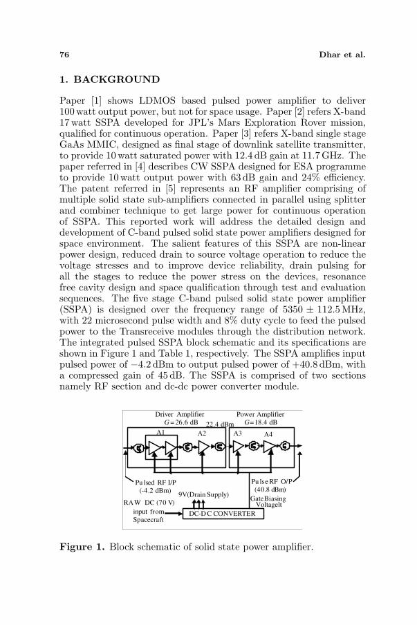
76 Dhar et al.
1. BACKGROUND
Paper [1] shows LDMOS based pulsed power amplifier to deliver100watt output power, but not for space usage. Paper [2] refers X-band17watt SSPA developed for JPL’s Mars Exploration Rover mission,qualified for continuous operation. Paper [3] refers X-band single stageGaAs MMIC, designed as final stage of downlink satellite transmitter,to provide 10 watt saturated power with 12.4 dB gain at 11.7GHz. Thepaper referred in [4] describes CW SSPA designed for ESA programmeto provide 10watt output power with 63 dB gain and 24% efficiency.The patent referred in [5] represents an RF amplifier comprising ofmultiple solid state sub-amplifiers connected in parallel using splitterand combiner technique to get large power for continuous operationof SSPA. This reported work will address the detailed design anddevelopment of C-band pulsed solid state power amplifiers designed forspace environment. The salient features of this SSPA are non-linearpower design, reduced drain to source voltage operation to reduce thevoltage stresses and to improve device reliability, drain pulsing forall the stages to reduce the power stress on the devices, resonancefree cavity design and space qualification through test and evaluationsequences. The five stage C-band pulsed solid state power amplifier(SSPA) is designed over the frequency range of 5350 ± 112.5MHz,with 22 microsecond pulse width and 8% duty cycle to feed the pulsedpower to the Transreceive modules through the distribution network.The integrated pulsed SSPA block schematic and its specifications areshown in Figure 1 and Table 1, respectively. The SSPA amplifies inputpulsed power of −4.2 dBm to output pulsed power of +40.8 dBm, witha compressed gain of 45 dB. The SSPA is comprised of two sectionsnamely RF section and dc-dc power converter module.
Driver
G = 26.6 dB
Power
G=18.4 dB22.4 dBm
Pu lsed RF I/P
(-4.2 dBm)
Pu lse RF O/P
(40.8 dBm)
DC-D C CONVERTER
RAW DC (70 V)
input from
Spacecraft
9V (Drain Supply)Gate Biasing
Voltagelt
A1 A3A2 A4
Amplifier Amplifier
Figure 1. Block schematic of solid state power amplifier.
Progress In Electromagnetics Research Letters, Vol. 23, 2011 77
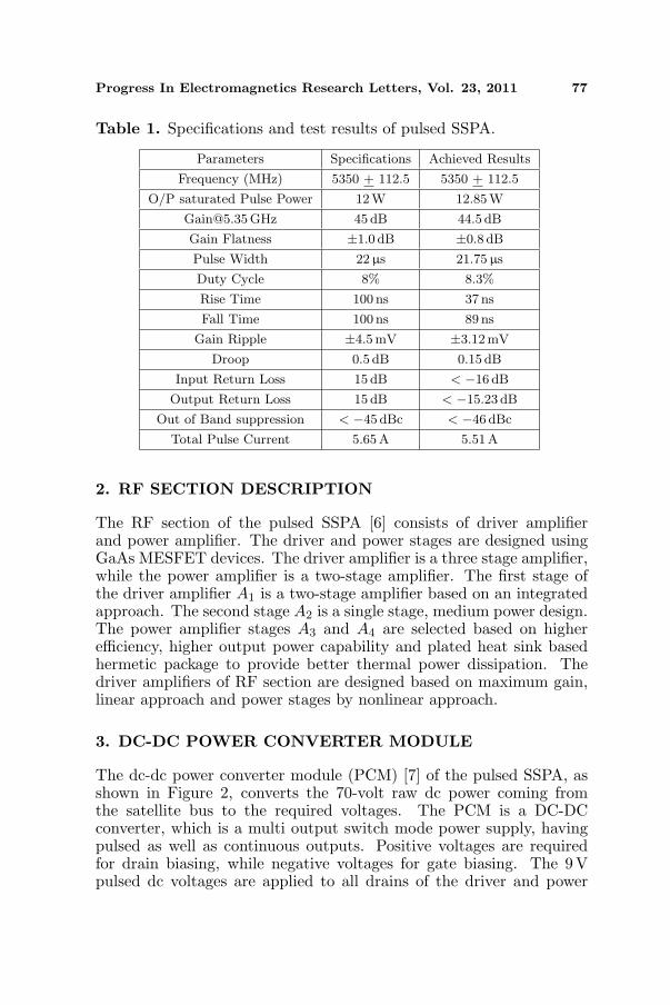
Table 1. Specifications and test results of pulsed SSPA.
Parameters Specifications Achieved Results
Frequency (MHz) 5350 + 112.5 5350 + 112.5
O/P saturated Pulse Power 12W 12.85W
[email protected] 45 dB 44.5 dB
Gain Flatness ±1.0 dB ±0.8 dB
Pulse Width 22 µs 21.75 µs
Duty Cycle 8% 8.3%
Rise Time 100 ns 37 ns
Fall Time 100 ns 89 ns
Gain Ripple ±4.5mV ±3.12mV
Droop 0.5 dB 0.15 dB
Input Return Loss 15 dB < −16 dB
Output Return Loss 15 dB < −15.23 dB
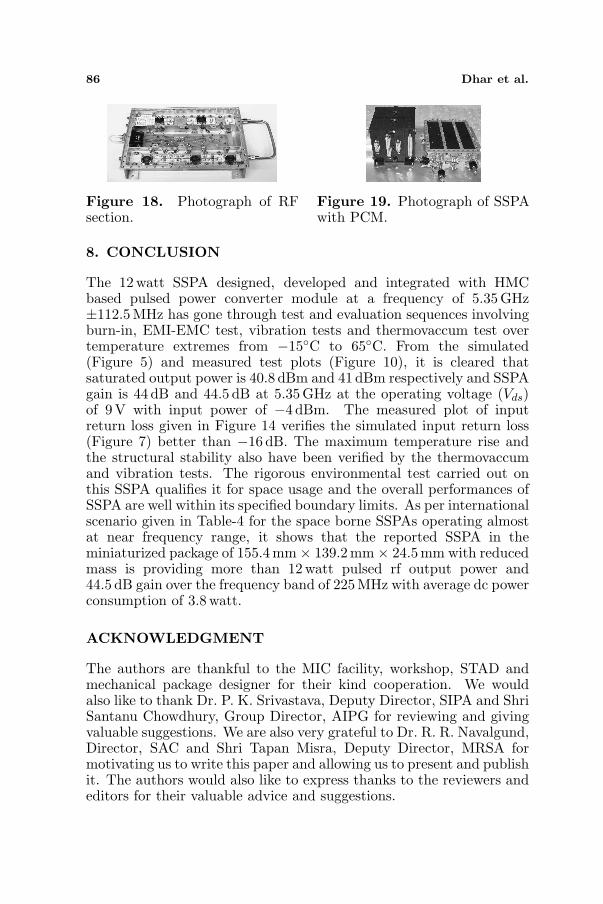
Out of Band suppression < −45 dBc < −46 dBc
Total Pulse Current 5.65A 5.51A
2. RF SECTION DESCRIPTION
The RF section of the pulsed SSPA [6] consists of driver amplifierand power amplifier. The driver and power stages are designed usingGaAs MESFET devices. The driver amplifier is a three stage amplifier,while the power amplifier is a two-stage amplifier. The first stage ofthe driver amplifier A1 is a two-stage amplifier based on an integratedapproach. The second stage A2 is a single stage, medium power design.The power amplifier stages A3 and A4 are selected based on higherefficiency, higher output power capability and plated heat sink basedhermetic package to provide better thermal power dissipation. Thedriver amplifiers of RF section are designed based on maximum gain,linear approach and power stages by nonlinear approach.
3. DC-DC POWER CONVERTER MODULE
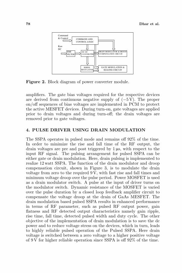
The dc-dc power converter module (PCM) [7] of the pulsed SSPA, asshown in Figure 2, converts the 70-volt raw dc power coming fromthe satellite bus to the required voltages. The PCM is a DC-DCconverter, which is a multi output switch mode power supply, havingpulsed as well as continuous outputs. Positive voltages are requiredfor drain biasing, while negative voltages for gate biasing. The 9 Vpulsed dc voltages are applied to all drains of the driver and power
78 Dhar et al.
.
COMMAND AND
CONTROL LOGIC
EMI
FILTER
DC-DC
CONVER TER
DRAIN MODULATOR & DROO P
CO MPENSATION CIRCUIT
SERIES
REGULATOR
GATE MODULATION &
BIASING CIRCUIT
Raw
DC
Command
& Control
Figure 2. Block diagram of power converter module.
amplifiers. The gate bias voltages required for the respective devicesare derived from continuous negative supply of (−5V). The properon/off sequences of bias voltages are implemented in PCM to protectthe active MESFET devices. During turn-on, gate voltages are appliedprior to drain voltages and during turn-off; the drain voltages areremoved prior to gate voltages.
4. PULSE DRIVER USING DRAIN MODULATION
The SSPA operates in pulsed mode and remains off 92% of the time.In order to minimize the rise and fall time of the RF output, thedrain voltages are pre and post triggered by 1µs, with respect to theinput RF signal. The pulsing arrangement for pulsed SSPA can beeither gate or drain modulation. Here, drain pulsing is implemented torealize 12watt SSPA. The function of the drain modulator and droopcompensation circuit, shown in Figure 3, is to modulate the drainvoltage from zero to the required 9 V, with fast rise and fall times andminimum voltage droop over the pulse period. Power MOSFET is usedas a drain modulator switch. A pulse at the input of driver turns onthe modulator switch. Dynamic resistance of the MOSFET is variedover the pulse duration by a closed loop feedback amplifier circuit tocompensate the voltage droop at the drain of GaAs MESFET. Thedrain modulation based pulsed SSPA results in enhanced performancein terms of RF parameter, such as pulsed RF output power, gainflatness and RF detected output characteristics namely gain ripple,rise time, fall time, detected pulsed width and duty cycle. The otherobjective of the implementation of drain modulation is to save the dcpower and to reduce voltage stress on the devices, which in turn, leadsto highly reliable pulsed operation of the Pulsed SSPA. Here drainvoltage is switched between a zero voltage to a higher positive voltageof 9 V for higher reliable operation since SSPA is off 92% of the time.
Progress In Electromagnetics Research Letters, Vol. 23, 2011 79
5. LINEAR AND NONLINEAR DESIGN ANDSIMULATION
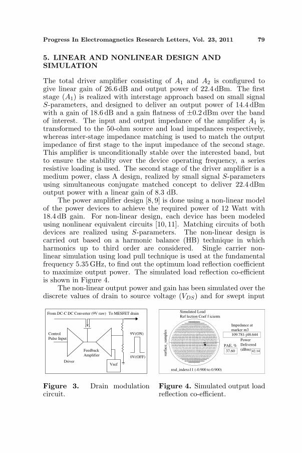
The total driver amplifier consisting of A1 and A2 is configured togive linear gain of 26.6 dB and output power of 22.4 dBm. The firststage (A1) is realized with interstage approach based on small signalS-parameters, and designed to deliver an output power of 14.4 dBmwith a gain of 18.6 dB and a gain flatness of ±0.2 dBm over the bandof interest. The input and output impedance of the amplifier A1 istransformed to the 50-ohm source and load impedances respectively,whereas inter-stage impedance matching is used to match the outputimpedance of first stage to the input impedance of the second stage.This amplifier is unconditionally stable over the interested band, butto ensure the stability over the device operating frequency, a seriesresistive loading is used. The second stage of the driver amplifier is amedium power, class A design, realized by small signal S-parametersusing simultaneous conjugate matched concept to deliver 22.4 dBmoutput power with a linear gain of 8.3 dB.
The power amplifier design [8, 9] is done using a non-linear modelof the power devices to achieve the required power of 12 Watt with18.4 dB gain. For non-linear design, each device has been modeledusing nonlinear equivalent circuits [10, 11]. Matching circuits of bothdevices are realized using S-parameters. The non-linear design iscarried out based on a harmonic balance (HB) technique in whichharmonics up to third order are considered. Single carrier non-linear simulation using load pull technique is used at the fundamentalfrequency 5.35GHz, to find out the optimum load reflection coefficientto maximize output power. The simulated load reflection co-efficientis shown in Figure 4.
The non-linear output power and gain has been simulated over thediscrete values of drain to source voltage (VDS) and for swept input
Vref
From DC-C DC Converter (9V raw) To MESFET drain
9V(ON)
0V(OFF)
Feedback
Amplifier
Driver
Control
Pulse Input
Figure 3. Drain modulationcircuit.
m3
Simulated Load
Ref lection Coef f icients
surf
ace_
sam
ple
s
real_indexs11 (-0.900 to 0.900)
PAE, %
37.60
Impedance at
marker m3
109.781-j48.644
Power
Delivered
(dBm) 42.14
Figure 4. Simulated output loadreflection co-efficient.
80 Dhar et al.
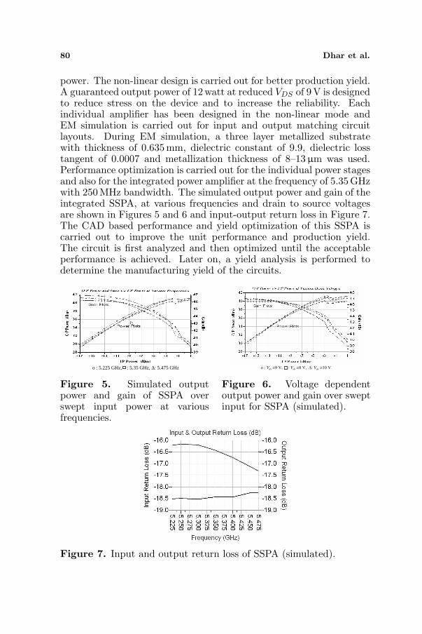
power. The non-linear design is carried out for better production yield.A guaranteed output power of 12 watt at reduced VDS of 9V is designedto reduce stress on the device and to increase the reliability. Eachindividual amplifier has been designed in the non-linear mode andEM simulation is carried out for input and output matching circuitlayouts. During EM simulation, a three layer metallized substratewith thickness of 0.635 mm, dielectric constant of 9.9, dielectric losstangent of 0.0007 and metallization thickness of 8–13µm was used.Performance optimization is carried out for the individual power stagesand also for the integrated power amplifier at the frequency of 5.35 GHzwith 250MHz bandwidth. The simulated output power and gain of theintegrated SSPA, at various frequencies and drain to source voltagesare shown in Figures 5 and 6 and input-output return loss in Figure 7.The CAD based performance and yield optimization of this SSPA iscarried out to improve the unit performance and production yield.The circuit is first analyzed and then optimized until the acceptableperformance is achieved. Later on, a yield analysis is performed todetermine the manufacturing yield of the circuits.
o : 5.225 GHz, : 5.35 GHz, ∆: 5.475 GHz
Figure 5. Simulated outputpower and gain of SSPA overswept input power at variousfrequencies.
o : V =9 V, : V =8 V, ∆: V =10 Vds dsds
Figure 6. Voltage dependentoutput power and gain over sweptinput for SSPA (simulated).
Figure 7. Input and output return loss of SSPA (simulated).
Progress In Electromagnetics Research Letters, Vol. 23, 2011 81
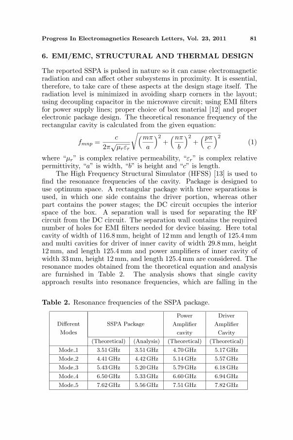
6. EMI/EMC, STRUCTURAL AND THERMAL DESIGN
The reported SSPA is pulsed in nature so it can cause electromagneticradiation and can affect other subsystems in proximity. It is essential,therefore, to take care of these aspects at the design stage itself. Theradiation level is minimized in avoiding sharp corners in the layout;using decoupling capacitor in the microwave circuit; using EMI filtersfor power supply lines; proper choice of box material [12] and properelectronic package design. The theoretical resonance frequency of therectangular cavity is calculated from the given equation:
fmnp =c
2π√
µrεr
√(mπ
a
)2+
(nπ
b
)2+
(pπ
c
)2(1)
where “µr” is complex relative permeability, “εr” is complex relativepermittivity, “a” is width, “b” is height and “c” is length.
The High Frequency Structural Simulator (HFSS) [13] is used tofind the resonance frequencies of the cavity. Package is designed touse optimum space. A rectangular package with three separations isused, in which one side contains the driver portion, whereas otherpart contains the power stages; the DC circuit occupies the interiorspace of the box. A separation wall is used for separating the RFcircuit from the DC circuit. The separation wall contains the requirednumber of holes for EMI filters needed for device biasing. Here totalcavity of width of 116.8 mm, height of 12 mm and length of 125.4mmand multi cavities for driver of inner cavity of width 29.8 mm, height12mm, and length 125.4 mm and power amplifiers of inner cavity ofwidth 33mm, height 12 mm, and length 125.4 mm are considered. Theresonance modes obtained from the theoretical equation and analysisare furnished in Table 2. The analysis shows that single cavityapproach results into resonance frequencies, which are falling in the
Table 2. Resonance frequencies of the SSPA package.
Different
Modes
SSPA Package
Power
Amplifier
cavity
Driver
Amplifier
Cavity
(Theoretical) (Analysis) (Theoretical) (Theoretical)
Mode 1 3.51GHz 3.51 GHz 4.70GHz 5.17GHz
Mode 2 4.41GHz 4.42 GHz 5.14GHz 5.57GHz
Mode 3 5.43GHz 5.20 GHz 5.79GHz 6.18GHz
Mode 4 6.50GHz 5.33 GHz 6.60GHz 6.94GHz
Mode 5 7.62GHz 5.56 GHz 7.51GHz 7.82GHz
82 Dhar et al.
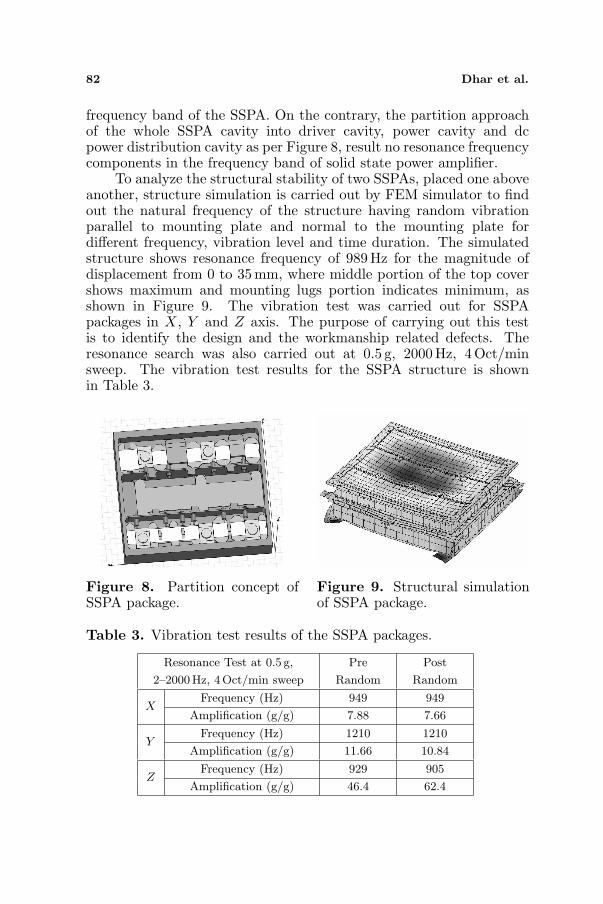
frequency band of the SSPA. On the contrary, the partition approachof the whole SSPA cavity into driver cavity, power cavity and dcpower distribution cavity as per Figure 8, result no resonance frequencycomponents in the frequency band of solid state power amplifier.
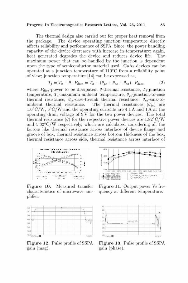
To analyze the structural stability of two SSPAs, placed one aboveanother, structure simulation is carried out by FEM simulator to findout the natural frequency of the structure having random vibrationparallel to mounting plate and normal to the mounting plate fordifferent frequency, vibration level and time duration. The simulatedstructure shows resonance frequency of 989 Hz for the magnitude ofdisplacement from 0 to 35 mm, where middle portion of the top covershows maximum and mounting lugs portion indicates minimum, asshown in Figure 9. The vibration test was carried out for SSPApackages in X, Y and Z axis. The purpose of carrying out this testis to identify the design and the workmanship related defects. Theresonance search was also carried out at 0.5 g, 2000 Hz, 4 Oct/minsweep. The vibration test results for the SSPA structure is shownin Table 3.
Figure 8. Partition concept ofSSPA package.
Figure 9. Structural simulationof SSPA package.
Table 3. Vibration test results of the SSPA packages.
Resonance Test at 0.5 g,
2–2000Hz, 4Oct/min sweep
Pre
Random
Post
Random
XFrequency (Hz) 949 949
Amplification (g/g) 7.88 7.66
YFrequency (Hz) 1210 1210
Amplification (g/g) 11.66 10.84
ZFrequency (Hz) 929 905
Amplification (g/g) 46.4 62.4
Progress In Electromagnetics Research Letters, Vol. 23, 2011 83
The thermal design also carried out for proper heat removal fromthe package. The device operating junction temperature directlyaffects reliability and performance of SSPA. Since, the power handlingcapacity of the device decreases with increase in temperature; again,heat generated degrades the device and reduces device life. Themaximum power that can be handled by the junction is dependentupon the type of semiconductor material used. GaAs devices can beoperated at a junction temperature of 110◦C from a reliability pointof view; junction temperature [14] can be expressed as,
Tj = Ta + θ · Pdiss = Ta + (θjc + θcs + θsa) · Pdiss (2)where Pdiss-power to be dissipated, θ-thermal resistance, Tj-junctiontemperature, Ta-maximum ambient temperature, θjc-junction-to-casethermal resistance, θcs-case-to-sink thermal resistance, θsa-sink-to-ambient thermal resistance. The thermal resistances (θjc) are1.6◦C/W, 5◦C/W and the operating currents are 4.1 A and 1 A at theoperating drain voltage of 9 V for the two power devices. The totalthermal resistance (θ) for the respective power devices are 1.82◦C/Wand 5.32◦C/W respectively, which are calculated considering all thefactors like thermal resistance across interface of device flange andgroove of box, thermal resistance across bottom thickness of the box,thermal resistance across side, thermal resistance across interface of
Figure 10. Measured transfercharacteristics of microwave am-plifier.
5.225 5.250 5.275 5.300 5.325 5.350 5.375 5.400 5.425 5.450 5.475
41.50
41.00
40.50
40.00
O/P
Po
wer
(d
Bm
)
Temp=-20 deg celsiusTemp=-15 deg celsiusTemp=+25 deg celsiusTemp=+55 deg celsiusTemp=+60 deg celsius
Frequency (GHz)
V =-1.34 V, g1 V =-1.34 V, g2 V =-0.91 V, g3
V =-1.21 V, g4 V =-1.34 V g5
Figure 11. Output power Vs fre-quency at different temperature.
Figure 12. Pulse profile of SSPAgain (mag).
Figure 13. Pulse profile of SSPAgain (phase).
84 Dhar et al.
Figure 14. Pulse profile of S11 (mag).
Figure 15. Rise time of thedetected signal.
Figure 16. Fall time of thedetected signal.
box and heat sink surface. The power dissipation for power devicesare 0.72 and 2.95 watt for 8% duty cycle. The calculated junctiontemperature for the power devices is 56 and 70◦C, where maximumtemperature rise will be for the final power device. The measured casetemperature of the final power device is 65◦C, which is below 110◦C.
7. DESIGN VALIDATION AND MEASUREMENT OF RFAND PULSE PROFILE
The Flight Model SSPA is developed using space grade components.Alumina substrate with three-layer metallization (Cr-Cu-Au) isselected due to high dielectric constant (9.8), low loss tangent (tan δ)0.0007, high thermal conductivity (0.37 W/cm/◦C) and its ruggednessat high temperatures. The passive chip components are assembledon the substrate by reflow soldering. The SSPA box is fabricatedusing Aluminium alloy 6061 T. The size and weight of the SSPAis 156 × 140 × 25.4mm3 and 400 g. The integrated pulsed SSPAis tested with PCM. The output power and gain at three differentfrequencies are displayed in Figure 10 and frequency dependent pulsed
Progress In Electromagnetics Research Letters, Vol. 23, 2011 85
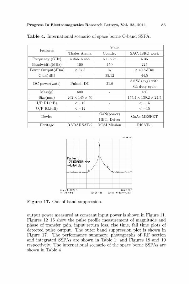
Table 4. International scenario of space borne C-band SSPA.
FeaturesMake
Thales Alenia Comdev SAC, ISRO work
Frequency (GHz) 5.355–5.455 5.1–5.25 5.35
Bandwidth(MHz) 100 150 225
Power Output(dBm) ≥ 37.8 37 ≥ 40.8 dBm
Gain( dB) - 35.12 44.5
DC power(watt) Pulsed, DC 21.93.8W (avg) with
8% duty cycle
Mass(g) 600 - 450
Size(mm) 262× 145× 50 155.4× 139.2× 24.5
I/P RL(dB) < −19 - < −15
O/P RL(dB) < −12 - < −15
Device -GaN(power)
HBT, DriverGaAs MESFET
Heritage RADARSAT-2 M3M Mission RISAT-1
Figure 17. Out of band suppression.
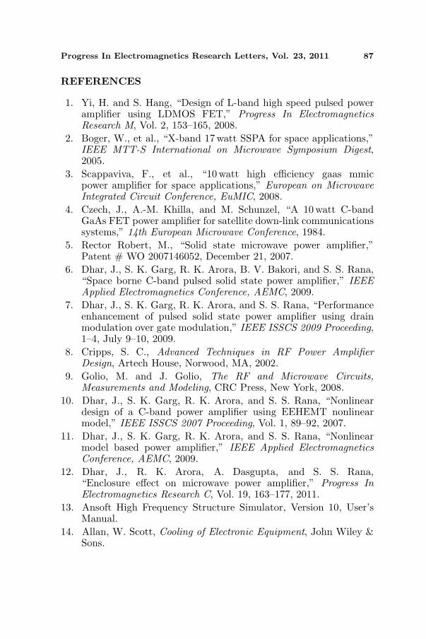
output power measured at constant input power is shown in Figure 11.Figures 12–16 show the pulse profile measurement of magnitude andphase of transfer gain, input return loss, rise time, fall time plots ofdetected pulse output. The outer band suppression plot is shown inFigure 17. The performance summary, photographs of RF sectionand integrated SSPAs are shown in Table 1; and Figures 18 and 19respectively. The international scenario of the space borne SSPAs areshown in Table 4.
86 Dhar et al.
Figure 18. Photograph of RFsection.
Figure 19. Photograph of SSPAwith PCM.
8. CONCLUSION
The 12 watt SSPA designed, developed and integrated with HMCbased pulsed power converter module at a frequency of 5.35 GHz±112.5MHz has gone through test and evaluation sequences involvingburn-in, EMI-EMC test, vibration tests and thermovaccum test overtemperature extremes from −15◦C to 65◦C. From the simulated(Figure 5) and measured test plots (Figure 10), it is cleared thatsaturated output power is 40.8 dBm and 41 dBm respectively and SSPAgain is 44 dB and 44.5 dB at 5.35GHz at the operating voltage (Vds)of 9 V with input power of −4 dBm. The measured plot of inputreturn loss given in Figure 14 verifies the simulated input return loss(Figure 7) better than −16 dB. The maximum temperature rise andthe structural stability also have been verified by the thermovaccumand vibration tests. The rigorous environmental test carried out onthis SSPA qualifies it for space usage and the overall performances ofSSPA are well within its specified boundary limits. As per internationalscenario given in Table-4 for the space borne SSPAs operating almostat near frequency range, it shows that the reported SSPA in theminiaturized package of 155.4mm× 139.2mm× 24.5mm with reducedmass is providing more than 12 watt pulsed rf output power and44.5 dB gain over the frequency band of 225 MHz with average dc powerconsumption of 3.8watt.
ACKNOWLEDGMENT
The authors are thankful to the MIC facility, workshop, STAD andmechanical package designer for their kind cooperation. We wouldalso like to thank Dr. P. K. Srivastava, Deputy Director, SIPA and ShriSantanu Chowdhury, Group Director, AIPG for reviewing and givingvaluable suggestions. We are also very grateful to Dr. R. R. Navalgund,Director, SAC and Shri Tapan Misra, Deputy Director, MRSA formotivating us to write this paper and allowing us to present and publishit. The authors would also like to express thanks to the reviewers andeditors for their valuable advice and suggestions.
Progress In Electromagnetics Research Letters, Vol. 23, 2011 87
REFERENCES
1. Yi, H. and S. Hang, “Design of L-band high speed pulsed poweramplifier using LDMOS FET,” Progress In ElectromagneticsResearch M, Vol. 2, 153–165, 2008.
2. Boger, W., et al., “X-band 17 watt SSPA for space applications,”IEEE MTT-S International on Microwave Symposium Digest,2005.
3. Scappaviva, F., et al., “10 watt high efficiency gaas mmicpower amplifier for space applications,” European on MicrowaveIntegrated Circuit Conference, EuMIC, 2008.
4. Czech, J., A.-M. Khilla, and M. Schunzel, “A 10watt C-bandGaAs FET power amplifier for satellite down-link communicationssystems,” 14th European Microwave Conference, 1984.
5. Rector Robert, M., “Solid state microwave power amplifier,”Patent # WO 2007146052, December 21, 2007.
6. Dhar, J., S. K. Garg, R. K. Arora, B. V. Bakori, and S. S. Rana,“Space borne C-band pulsed solid state power amplifier,” IEEEApplied Electromagnetics Conference, AEMC, 2009.
7. Dhar, J., S. K. Garg, R. K. Arora, and S. S. Rana, “Performanceenhancement of pulsed solid state power amplifier using drainmodulation over gate modulation,” IEEE ISSCS 2009 Proceeding,1–4, July 9–10, 2009.
8. Cripps, S. C., Advanced Techniques in RF Power AmplifierDesign, Artech House, Norwood, MA, 2002.
9. Golio, M. and J. Golio, The RF and Microwave Circuits,Measurements and Modeling, CRC Press, New York, 2008.
10. Dhar, J., S. K. Garg, R. K. Arora, and S. S. Rana, “Nonlineardesign of a C-band power amplifier using EEHEMT nonlinearmodel,” IEEE ISSCS 2007 Proceeding, Vol. 1, 89–92, 2007.
11. Dhar, J., S. K. Garg, R. K. Arora, and S. S. Rana, “Nonlinearmodel based power amplifier,” IEEE Applied ElectromagneticsConference, AEMC, 2009.
12. Dhar, J., R. K. Arora, A. Dasgupta, and S. S. Rana,“Enclosure effect on microwave power amplifier,” Progress InElectromagnetics Research C, Vol. 19, 163–177, 2011.
13. Ansoft High Frequency Structure Simulator, Version 10, User’sManual.
14. Allan, W. Scott, Cooling of Electronic Equipment, John Wiley &Sons.