Embed Size (px)
Citation preview

Tyco Laboratories, Inc.16 Hickory Drive
Waltham, Massachusetts 02154
THICK FILM SILICON GROWTH TECHNIQUES
by
H. E. BatesF. H. Cocks
A. I. MlavskyF. Wald
cC opv%^f i^ •
Second Quarterly Progress ReportSubcontract No. 953365
Covering Period: 1 June 1972 - 31 August 1972
This work was performed for the Jet Propulsion Laboratory, CaliforniaInstitute of Technology, sponsored by the National Aeronautics and SpaceAdministration under Contract NAS7-100.
https://ntrs.nasa.gov/search.jsp?R=19720025068 2018-08-25T20:10:06+00:00Z

This report contains information prepared by Tyco Laboratories, Inc. underJPL subcontract No. 953365. Its content is not necessarily endorsed by the JetPropulsion Laboratory, California Institute of Technology, or the National Aeronauticsand Space Administration.

Tyco Laboratories, Inc.16 Hickory Drive
Waltham, Massachusetts 02154
THICK FILM SILICON GROWTH TECHNIQUES
by
H. E. BatesF. H. Cocks
A. I. MlavskyF. Wald
Second Quarterly Progress ReportContract No. 953365
Covering Period: 1 June 1972 - 31 August 1972
This work was performed for the Jet Propulsion Laboratory, CaliforniaInstitute of Technology, sponsored by the National Aeronautics and SpaceAdministration under Contract NAS7-100

ABSTRACT
During this period, silicon ribbon growth experiments were conducted using
orifices (dies) fabricated from SiC-SiO0 mixtures, fused quartz, SiC, and fine-Ct
grained, high density graphite. The best results were obtained from graphite dies.
A number of different approaches was tried in modifying the thermal gradient inthe dies and in holding the dies. The best results here were obtained from a 0.25-in.
thick Mo disc holding a graphite die directly and fitting the die quite closely. Ribbon
growths as wide as 9 mm were obtained, while the longest ribbon was 450 x 3.5 x
0.5 mm. Resistivities of ribbons grown from graphite dies have been measured over
the range of 0.03 to 1.6 n-cm. Some thoughts and literature findings are presentedregarding refractory oxide materials as potential orifices.
111

Table of Contents
Section Page No.
ABSTRACT ii
I. SUMMARY 1
II. INTRODUCTION 3
III. TECHNICAL DISCUSSION 7
A. Die Materials 7
B. Thermal Design 9
C. Orifice Design 14
D. Ribbon Growths 14
E. New Orifice Materials 19
IV. CONCLUSIONS AND RECOMMENDATIONS 23
V. NEW TECHNOLOGY 25
VI. REFERENCES 27

List of Illustrations
Figure No. Page No.
1. Schematic drawing showing crucible and die arrangementfor edge-defined, film-fed growth (EFG) ofsilicon ribbon 4
2a. Components of ribbon growth setup 10
2b. Top view of assembled setup showing position of orificein lid. Afterheater and radiation shield have been omittedfor clarity 10
3. Ribbons grown from graphite dies 11
4. Ribbon C-57, grown from a graphite die 12
5. Orifice design being used currently 15
6. Surfaces of C-57 ribbons showing lateral striationsfrom vibration and SiC crystallite pickup on top andbottom ribbons 18
VII

I. SUMMARY
A substantial effort was expended in this quarter on growth experiments with
a variety of orifice materials. These included SiC-SiO0 mixtures in the ratios oftt
95:5, 90:10, 60:40, and 20:80; fused quartz; SiC made by pyrolytic conversion of
graphite; and high purity, high density graphite. Wetting experiments had indicated
very favorable behavior of the 20% SiC-80% SiCL material. However, this was not
borne out in actual performance as an orifice . The major difficulty with the 20%
SiC-80% SiO2 (and to an even greater extent, with 60% SiC-40% SiCL) material wasformation of massive amounts of SiO in the vicinity of the orifice. This was appar-
ently the result of reduction of the SiCL by the SiC. Also, the excellent wetting of
these materials resulted in poor edge definition when any growth could be obtained
and difficulties in working with orifices, since they became entirely covered with
molten Si during an experiment. For these reasons, these materials were dropped
from further consideration.
Experiments with the lower SiCL content materials were essentially a con-
tinuation of the effort begun in the preceding quarter to define a set of suitable growth
parameters with materials with known shortcomings. A number-of experiments were
run with various modifications to the way in which the orifice is held and to the means
of heat transfer to and from the orifice. These experiments were generally un-
successful insofar as direct attempts were made to influence the temperature gradient
across the orifice. Then, however, the approach was changed attempting to produce
a uniform temperature by bringing the molybdenum support structure as close as
possible to the orifice and consolidating a number of shields into one. This has
yielded a marked improvement in the initiation and stability of growth, particularly
with graphite orifices.One experiment was done using an orifice made from a form of high purity
SiC produced by heating graphite in the presence of silane or silicones.* The orifice
*Pyrobond TM of Dow-Corning Corporation.

was not of typical design and the ribbon grown was unexceptional; however, its
resistivity was 0.16 n-cm and the rate of dissolution/precipitation of the SiC did
appear to be lower than with the hot-pressed materials.
Fused quartz orifices were tried in four experiments. All were unsuccessful.
The major problems were inability to produce a uniform, high temperature (i.e.,greater than the melting point of Si) over the entire orifice and the unpredictable
wetting of quartz by Si. It is possible, however, that recent changes in the thermal
configuration of growth setups may permit solid quartz dies to work. Alternative
approaches using a duplex structure of pyrolytic graphite and quartz are also being
planned.
While graphite dies appear to be effective, it must be remembered that
ultimately such dies will "wear out" by reaction and dissolution. The useful life of
a graphite die and the parameters affecting it remain to be determined; however, itis clear that a more stable material is desirable. Results obtained by other investi-
gators indicate that beryllium oxide may be a usable orifice material in that there is
partial wetting, no apparent reaction with Si, and reasonable doping behavior by Be.
We intend to investigate this material closely and also to examine some other oxides,
at least on the basis of their relative stability and the stability of their silicides.
This group will initially comprise CaO, and YgCL. Other oxides may be included as
they are revealed from literature findings.

II. INTRODUCTION
One primary limitation to the large scale use of silicon solar cells in gene-rating electric power from sunlight has been the lack of an industrially feasibletechnique in which thin, single crystal silicon ribbons are grown directly and con-tinuously from the melt. Many attempts have been made previously to overcome thislimitation. These attempts have included such methods as controlled dendritic growth
1-6 79into supercooled silicon and the use of non-wetting shaping dies. ' This lattermethod, in particular, is very closely related to the Stepanov method which,independently of American efforts, has been applied to silicon ribbon growth byRussian workers. ' The former method, while capable of producing silicon rib-bon, does not appear promising from the point of view of producing large amounts ofinexpensive silicon ribbons for solar cell applications. This is so primarily becauseof the difficulty of maintaining stable ribbon growth, since, in the web-dendritemethod, it is necessary to maintain growth temperatures constant to ± 0.02°C, thusmaking crucible replenishment practically impossible. Ribbon growth based on theuse of essentially non-wetting dies in combination with edge-definition offers pros-pects for economical silicon ribbon fabrication. However, a considerable effort atthe basic research level will first be required to establish the microdynamics ofshape stability. As we will show, the EFG method overcomes the need for refinedtemperature control during growth and provides a more inherently stable growthprocess than previous shaped growth methods. Concomitantly, however, the EFGprocess puts stringent requirements on the nature of the die material if semicon-
ductor purity levels are to be met.Edge-defined, film fed growth (EFG) is a process by which single crystals
may be grown having a shape controlled by the outside dimensions of a die, thegrowth actually taking place from an extremely thin film of liquid fed by capillary
12 -1Raction from a crucible below. The application of this method to the growth ofcrystals with a ribbon geometry is illustrated in Fig. 1. The procedure is as follows.

SILICONSINGLE CRYSTAL
RIBBON
SUPPORTINGPLATE FOR RIBBON DIE
QUARTZCRUCIBLE
INSIDESUSCEPTOR
LIQUID SILICONGROWTH FILM
R.FHEATINGCOIL
CAPILLARY DIE FOR RIBBONGROWTH
Fig. 1. Schematic drawing showing crucible and die arrangementfor edge-defined, film-fed growth (EFG) of silicon ribbon
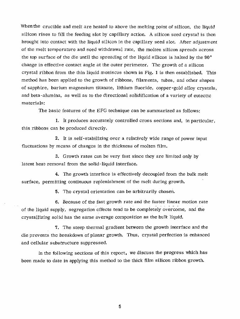
When the crucible and melt are heated to above the melting point of silicon, the liquidsilicon rises to fill the feeding slot by capillary action. A silicon seed crystal is thenbrought into contact with the liquid silicon in the capillary seed slot. After adjustmentof the melt temperature and seed withdrawal rate, the molten silicon spreads acrossthe top surface of the die until the spreading of the liquid silicon is halted by the 90°change in effective contact angle at the outer perimeter. The growth of a siliconcrystal ribbon from the thin liquid meniscus shown in Fig. 1 is then established. Thismethod has been applied to the growth of ribbons, filaments, tubes, and other shapesof sapphire, barium magnesium titanate, lithium fluoride, copper-gold alloy crystals,and beta-alumina, as well as to the directional solidification of a variety of eutecticmaterials:
The basic features of the EFG technique can be summarized as follows:
1. It produces accurately controlled cross sections and, in particular,thin ribbons can be produced directly.
2. It is self-stabilizing over a relatively wide range of power inputfluctuations by means of changes in the thickness of molten film.
3. Growth rates can be very fast since they are limited only bylatent heat-removal from the solid-liquid interface.
4. The growth interface is effectively decoupled from the bulk meltsurface, permitting continuous replenishment of the melt during growth.
5. The crystal orientation can be arbitrarily chosen.
6. Because of the fast growth rate and the faster linear motion rateof the liquid supply, segregation effects tend to be completely overcome, and thecrystallizing solid has the same average composition as the bulk liquid.
7. The steep thermal gradient between the growth interface and thedie prevents the breakdown of planar growth. Thus, crystal perfection is enhanced
and cellular substructure suppressed.
In the following sections of this report, we discuss the progress which hasbeen made to date in applying this method to the thick film silicon ribbon growth.

III. TECHNICAL DISCUSSION
A. Die Materials
1. Si02
Production of an effective quartz die was approached from threedirections. We attempted to produce coatings of SiO0 on refractory metals and SiC
£t
by pyrolysis of silane in the presence of oxygen. The quartz films we were able toget were too thin and/or too porous to resist molten silicon. This coupled with aslow deposition rate led us to drop this technique.
Several attempts were made to fabricate orifices from hot-pressed mixturesof SiCL/Si in ratios of 5, 10, and 30% Si. These were all unsuccessful due to the lowstrength of the mixtures. Tests of the wettability of these materials by Si showed atendency for the Si within the structure to run out when molten and for the material towarp when it was in pieces the thickness of typical orifices.
Finally, four runs were made with solid fused quartz orifices, both one- andtwo-piece. The inner surfaces of the orifices were variously pre-treated by sand-
blasting and coating with a thin wash of collodal graphite to promote wetting. Inaddition, thin slabs of silicon were positioned in the feed slots of the orifices to pro-
vide some silicon to fill the orifice on melting. The basic difficulty encountered inall four experiments was that the silicon would not feed up the capillary slots until thetemperature had been raised to the softening point of the quartz. Even when pressedto this extreme, the wetting and feeding were unpredictable. The problem wouldappear to be the low thermal conductivity of quartz compounded with the difficultwetting. For this reason, quartz was suspended from active consideration; howeverwe now feel that recent advancements in thermal design made with graphite dies mayallow use of fused quartz. Also, we are considering some alternate die structures of
quartz and pyrolytic graphite.

2. SiC-SiOg mixtures
Wetting experiments with an 80% SiCL-20% SiC hot-pressed mixture
showed an apparently small amount of SiC dissolution/precipitation and excellent
wetting. Orifices were fabricated from this material and tried. Two significant
difficulties were experienced with this material. First, wetting by the Si was so
good that eventually the entire die became covered with molten Si which made it
inconveniently difficult to hold the dies in isolation from the molybdenum parts.
This also resulted in poor edge definition when any growth could be achieved; essen-tially, growth occurred from a puddle of silicon. Secondly, during an experiment,
massive amounts of SiO were deposited near the orifice. This apparently resulted
from reduction of the SiO2 by SiC. The effect was to seriously distort the thermal
conditions at the orifice, generally precluding growth. Dies made from 60% SiC-
40% SiO, behaved in a similar fashion, with even greater amounts of SiO forming.
For this reason, we are no longer considering these materials.
3. SiC - Pyrobond*©
We obtained some sample pieces of a material made by exposing
high purity graphite to gaseous silicon at high temperatures. The reaction product,SiC, occurs as a case on the graphite some 0.020 to 0.030 in. deep. The SiC is
nominally as pure as the graphite from which it is made. Fixtures treated by this
process find wide application for high temperature processing in semiconductor
device fabrication. We were able to make a die by slicing two slabs from a piece
such that L-shaped sections resulted. The graphite core was burned away at 1000 °C
in air, and the pieces were prewetted with Si and assembled. Three pieces of Si
were grown from this makeshift die. Their average resistivity was 0.16 n-cm,
approximately ten times that of the majority of ribbons grown from hot-pressed SiC.
It is not clear that this particular piece represented the highest purity attainable by
the process, so we intend to have some of our graphite dies treated by the Pyrobondprocess. This should result in almost complete conversion to SiC because of the
generally thin sections in the dies. The performance of these dies will then be
evaluated.
*Pyrobond is a trademark of the Dow-Corning Corporation, Midland, Michigan.

4. Graphite
In light of the generally lackluster results from most SiC and SiCLdies, we decided to try graphite. Clearly, reaction to SiC was bound to occur, buta high density graphite would expose less total surface for reaction/solution than hadthe 70% dense hot-pressed SiC materials, so that conceivably a decrease in physicalcontamination might be realized. At the same time, since graphites can be producedat very high purity levels (and cleaned relatively easily), it was apparent that muchlower impurity levels could be achieved in Si grown from graphite.
Four experiments have been done to date with graphite orifices. All weredone with a 0.25-in. thick Mo cover/holding plate of the type shown in Fig. 2. Theorifices all fed very readily, and growth could be easily initiated. Reasonable widthswere grown in the first two experiments (Fig. 3), while in the third run, because ofa misalignment of the orifice, a width of only 3 to 4 mm could be obtained; however,a ribbon 45 cm long by 3.5 mm was grown at a rate of 2.6 cm per minute (Fig. 4).
The major problems encountered are: (1) that the setups, i.e., orifice, arefairly sensitive mechanically — they must be aligned and located with reasonableprecision; and (2) precipitation of SiC on the liquid meniscus affects the growthinterface and the surface of the ribbon — this seems to be somewhat amenable tocontrol by variation of the thermal conditions, but will always be present as long asthe graphite is exposed to liquid Si. We expect that substantial improvement ispossible in both of these problem areas and shall concentrate our efforts on makinggraphite viable as a near-term die material.
B. Thermal Design
A variety of configurations of lids, afterheaters, and direct modifiers weretested during this period.
Three runs were made using a graphite afterheater to supply heat to the seedand growing crystal. It had been observed previously that the addition of a "warm"Mo afterheater had exerted a strong influence on the growth process in the direction
of increased stability (this prior to the addition of the temperature controller). TheMo afterheater consisted of a cover with a large oval opening and a vertical Mo tube0.75 in. in diameter with a rectangular slot cut in the bottom to allow observation ofthe orifice. The cover ran at ~ 1500 °C and the tube operated with a vertical tem-perature gradient of about 1300° to 900° over 1.5 in. The graphite afterheater had

Fig. 2a. Components of ribbon growth setup. From left: graphite felt insulation,molybdenum susceptor, molybdenum afterheater with viewport, quartzcrucible, molybdenum lid, molybdenum radiation shield, graphite die.
Fig. 2b. Top view of assembled setup showing position of orifice in lid.Afterheater and radiation shield have been omitted for clarity.
10

Fig. 3. Ribbons grown from graphite dies, (a) C-55, (b) C-56.
11

Fig. 4. Ribbon C-57, grown from a graphite die. The piece nearestthe ruler grew stably for 18 in. at 1 in./min.
12

a single 0.5 in. hold in the wall for viewing the orifice. It ran at approximately 1500°C
for about 0.8 in. above the orifice, and cooled gradually to about 1000° over the re-maining 1.5 in. Given these conditions, it was extremely difficult to obtain stablegrowth and impossible to achieve spreading of the initial growth across the orifice.
These results were taken to mean that provision of a uniformly hot environment inthe vicinity of the orifice will inhibit growth by reversing the temperature gradientacross the orifice and reducing the effectiveness of the vertical gradient through theseed.
In another experiment, a deliberate modification of the gradient across theorifice was attempted by placing truncated wedges of boron nitride on the top coverplate at the ends of the orifice to block radiation from the susceptor. At the sametime, thin molybdenum radiation shields were positioned parallel to the central two-thirds of the orifice, spaced approximately 0.050 in. away. Unfortunately, theradiation shields, in operation, ran at a lower temperature than was expected, sotheir effectiveness was somewhat dubious. However, the boron nitride blocksappeared to serve their intended function. Only one side of the orifice was fed withmolten Si for some unknown reason; however, spreading of the initial growth towardthe end of the orifice was readily achieved, a clear indication that the outer end ofthe orifice was colder than the center.
Another series of three experiments were run with orifices which had anessentially solid top surface with only two small diameter feedholes near the center(similar to the "type a" orifice in Fig. 3 of the First Quarterly Report, save that thesides of the orifices were bevelled to give a flat surface on the top about 0.025 in.wide). These orifices were intended to test the theory that by limiting access of hotmolten Si to the center of the orifice, the center could be maintained hot relative tothe ends of the orifice. The results of two of the runs were inconclusive because ofdifficulties in feeding of the molten Si. The third experiment indicated that there wasno particularly strong influence from this orifice configuration. Lateral spreading
of the solid/liquid interface was not significantly easier than with orifices which arelargely open (i.e., subtended by molten Si) at the top.
The overall impact of these experiments led us to revert to a shielding con-
figuration used in early experiments with quite different orifices. This was anhourglass or "dogbone" shaped opening in the holding plates and heat shields whichleaves the ends of the orifice rather more distant from the molybdenum pieces
13

than is the center. Thus, the ends of the orifice receive less heat, transferred by
conduction/radiation inward from the susceptor, than the middle. This did not confer
any significant improvements in succeeding runs, so a different approach was taken,
based on our experiments with fused quartz orifices. There the problem was clearly
one of providing a uniform and sufficient amount of heat to the orifice to get it to feed.
We had used three 0.062 molybdenum lids stacked up and with rather narrow slots,
i.e., close to the orifice. It was then decided to replace this arrangement with a
single, thick (0.25 in.) lid. This was just tried with graphite dies, and the resultshave been encouraging enough that we shall try a configuration in which the clear-
ance between the molybdenum lid and the orifice is only a few thousands of an inch.
C. Orifice Design
The rate of evolution of the die design has slowed considerably and seems to
be settling on a configuration basically like that shown in Fig. 5. This design has a
number of obvious virtues in comparison to the two-piece type, not the least of
which are strength and constancy of the dimensions and relations of the edges of the
orifice. We are planning on eliminating the double rib and support plate and simply
engaging a single rib with a matching groove in the lid., This depends on our being
able to control spreading of the liquid Si out of the sides of the feed slot. The curva-
ture of the top edge of the orifice is an area which remains to be explored. We have
used flat orifices in our experiments with graphite dies, and it is unclear where
curvature of the orifice will help. We are having a variety of curvatures put on
some orifices for later experiments.
D. Ribbon Growths
1. Resistivity
Table I lists the resistivity measured on a number of ribbons grown
from a variety of orifice materials. It should be noted here that all the ribbons
examined have been p-type. The low resistivity of Si grown from the hot-pressed
SiC is consistent with earlier results. And it is apparent that incorporation of a
small amount of SiCL does not materially improve the situation. In the case of
Q-51, where a large amount of quartz has been substituted for SiC, a marked im-
provement results; however, as noted in II.A.2, this material appears to be im-
practical to use.
14

.30
.05
TYR
4.0
.4
.040
rs
FLAT.003 U/IOE:
.030JL
.470
Fig. 5. Orifice design being used currently. An 0.030-in. alumina plateengages the slot between the ribs on the sides of the orifice anditself rests in the recess in a holding plate.
15

Table I. Measured Resistivities of Silicon Ribbons Grownfrom a Variety of Die Materials
Ribbon
SC-30
SO 31
SG-32
SC-33
SO 34
SO 35
SO40
Q-51
SC -54
055
O56
057
O58
Die Material
SiC
SiC
SiC 4-10% SiO2
SiC
SiC
SiC
SiC 4 10% SiO2
80 Si02 + 20 SiC
Pyrobond® SiC
Poco Graphite*
AverageResistivity
( fi -cm)
0.008
0.012
0.026
0.014
0.015
0.025
0.050
1.10
0.15
0.53
0.045
0.030
1.6
Range ofResistivity Values
(fi -cm)
0.006 - 0.011
0.008 - 0.016
0.006 - 0.04
0.014 - 0.015
0.011 - 0.021
0.011 - 0.052
0.9 - 1.3
0.45 - 0.68
0.030 - 0.060
0.025 - 0.035
1.1 - 1.8
*Poco Graphite Corp., Decatur, Texas Grade AXF 5QBG1
16

Ribbon SC"-54 (actually three samples) indicates that Pyrobond SiC offers
some improvement over hot-pressed SiC. Probably further improvement can berealized if the initial purity of the basic graphite is closely controlled. We arehaving a few orifices made in this way to test this material fairly.
The graphite-or if ice grown ribbons present a seemingly inconsistent picture,without some explanation. Ribbons C-55 and C-58 were grown from dies supportedby sapphire holders, while C-56 and 57 had boron nitride pieces in place of thesapphire. It appears that the higher resistivities of 55 and 58 are the result ofpartial compensation of a p-type impurity in the graphite, while 56 and 57 simplyreceived additional doping from the boron nitride. The graphite dies were "cleaned"by firing ia argon at 1600 to 1700 °C. We intend in the near future to vacuum outgasthe dies.*
2. Ribbon surfaces
Physical contamination of the ribbon surfaces by included crystallitesof SiC continues to be a problem with any ribbon grown from a graphite or SiC die.Also, vibration in the pulling apparatus contributes its own irregularities. This canbe a particularly vexing problem given a pull rod/seed holder approximately 18 in.long with a 12-in. long ribbon growing at the end. Very slight vibrations becomeamplified considerably. Fig. 6, shows the three C-57 ribbons at almost twice life-size. The bright specks on the top and bottom ribbons are SiC crystallites, stuck tothe ribbon surface in many cases where a vibration has perturbed the meniscusslightly and shaken some of the SiC bits loose to float up onto the growth interface.The middle ribbon, grown, in fact, between the other two in time, shows a muchcleaner, almost mirror surface. The only difference was a slightly higher growthtemperature relative to the other ribbons. This had the unfortunate effect of de-stabilizing the growth, however, as can be seen from the irregular width. Thisis merely to illustrate that some degree of control may be possible in dealing withthis shortcoming in graphite dies. We feel that both problems can be dealt with tosignificantly improve the ribbon surfaces.
*Note added in proof: Subsequent ribbons grown from vacuum-baked dies withno holding plates have shown more consistent resistivities of approximately 1 to 3 n-cm.
17

JL, 1
1 I I I I
Fig. 6. Surfaces of C-57 ribbons showing lateral striations from vibrationand SiC crystallite pickup on top and bottom ribbons. Clean surfaceof middle ribbon (grown from the same orifice) is attributed tomodified growth conditions (~ 2X).
18

3. Crystallinity and perfection
Evaluation of the ribbons for crystalline perfection has been verysketchy during this period. Having now settled on what seems at least a workable die
material, we can begin to evaluate more thoroughly the ribbons grown from it. One
of the C-57 ribbons was X-rayed and found to be single crystal, but apparently theorientation of the seed had been lost in starting the growth, since the orientation of theribbon was not coincident with that of the seed. This is, however, an encouraging re-
" suit since the ribbon was grown at 1 in./min. Very obvious twins seem also to be aproblem, when conditions are such that precipitated SiC is included in or on the rib-bons. If, of course, we can reduce the SiC crystallite incidence, then this problemshould diminish.
E. New Orifice Materials
The apparent effectiveness of graphite dies is not without some equallyobvious drawbacks. It is an inescapable fact that liquid Si will react with graphite,and while it may be possible by careful design to minimize the temperatures through-out the setup and thus the reaction rate, it is still an unstable system. In continuingto experiment with quartz orifices, clearly we are trying to develop a more nearlyequilibrium system (although it should be remembered that quartz and liquid Si tendto react to SiO). It seems to still be desirable, however, to try to find a materialwhich does behave more stably than even quartz, if, in fact, such a material exists.
We have some indications that possibly beryllium oxide is non-reactive with17Si. For example, Kocher and Muhlbauer, in a study of the behavior of a variety
of materials as crucibles for melting high purity silicon, found no reaction, pene-tration, or corrosion of BeO crucibles by molten Si. Their only real.objections toBeO versus quartz were its cost and lack of transparency. They also said that they
were not able to grow as high purity (resistivity) crystals as from quartz. There is18
probably an explanation for this. Littlejohn and Robertson have reported a mini-mum resistivity of approximately 0.2 n-cm produced by diffusion of Be metal intoSi at 1300 °C. They claim that this represents the solubility limit for Be at 1300°,and that by reheating to lower temperatures, the resistivity could be increased toseveral n-cm by precipitating some of the Be. They also report room temperature
mobilities of 300 to 400 cm /V sec for carrier concentrations of 3 to 6 x 10 cm(4 to 2.6 J2-cm). Beryllium is a p-type dopant in Si. Thus, it appears that Si grownfrom BeO is probably doped with Be, which may account for Kocher's observations.
19

The interesting point is that there is apparently retrograde solubility of the Be.
Some other indications come from work by Kingery and co-workers who19 20investigated interfacial reactions and contact angles in a number of metal -
ceramic systems. Their findings for Si are summarized in Table II, adapted from
their papers. It would appear from their results, particularly on contact angles,that BeO is the most likely material, but it seems that TiCL and ThC^ are alsopossibilities. In addition, CaO, on the basis of the stability of the oxide and the
relative instability of the silicides, seems to be a possibility. Similar considerationsindicate that yttrium oxide should also be investigated.
These investigations will take the form initially of wetting/compatibilityexperiments and then move on to fabrication of dies and growth experiments withany promising-looking materials.
20

co .COfee
oo ITS c-o
o
e m COoo
oen
co
Inte
rfac
ial
Rea
ctio
ns
Pha
ses
Foun
d
CD>H3OJ(_,MCO
fl\£•
CD4-1CO:>,
CO
co0
CMi-H
<
•tCM
O•1-1CO
No
reac
tio
n
oo•*1-1
CO0
CXI
<1
•r"4CO
CMO• i-HCOCM
ICO
OCMi— i
3
Inte
rfac
ial
film
on
surf
ace;
slig
ht p
enet
ratio
n;
no
§CO1-1
corr
osio
nSl
ight
cor
rosi
on o
f ox
ide;
no
inte
rfac
ial
phas
e;
slig
ht p
ene-
trat
ion
alon
g gr
ain
boun
dari
es
ooCOi-H
Ofl)06•r^CO
ObD2
Slig
ht s
urfa
ce a
lter
atio
n
0o**iH
0bOs1
•r™4CO
•*O• rHCO
CM
fD
efin
ite i
nter
faci
al l
ayer
of
Mg2
SiO
4;
corr
osio
n of
oxi
de
0oCDr-l
Slig
ht s
urfa
ce
disc
olor
atio
n
0o•*iH
cfy->hiCO
c ..Sl
ight
rea
ctio
n w
ith d
ecre
ase
ipo
rosi
ty o
f ox
ide
near
sur
face
;
0oCO1-1
COCOrt-a&CO
8
e\O&
Sli
ght
reac
tion
and
adher
ence
oo•*1-1
ow
£iCO
i
Pen
etra
tion
of
met
alli
c ph
ase
betw
een
grai
n bo
unda
ries
and
blac
k di
scol
orat
ion
of g
rain
s;
0oCDi-l
corr
osio
n of
sur
face
CMO5nN
Th0•i-4CO!HN
Inte
rfac
ial
laye
r of
new
pha
se
oocoi-i
crInNiCO
21

IV. CONCLUSIONS AND RECOMMENDATIONS
During this period all the components of successful growth of silicon ribbonsuitable for solar cells have been achieved: stable growth for over 18 in., centi-meter wide growth, and resistivities in excess of 1 fl-cm. These results have beenachieved using graphite dies, which are not ideal but can clearly provide a meansto achieve the desired end of single crystal silicon ribbons.
During the next quarter our efforts will be concentrated in three areas:first, continued development of graphite dies and associated technology to producesolar cell quality Si ribbon; second, investigation of the feasibility of quartz dies;and third, investigation of the feasibility of using a more refractory oxide than quartz
as an orifice material.
23

V. NEW TECHNOLOGY
Description Title:
Names of Innovators:
Progress Reports:
Pages:
Date:
Improved Apparatus for the Edge-Defined, Film-
Fed Growth of Thick Film Silicon Ribbon from
Graphite Dies
H. E. Bates and V. White
Second Quarterly Report
6 through 10
August 1972
25

VI. REFERENCES
1. J. U. Faust, Jr., and H. F. John, J. Electrochem. Soc., 108, 860 (1961).
2. S. N. Dermatis and J. U. Faust, IEEE Trans. Commun. Electron, 65,194(1963). ~~
3. S. N. Dern, " Varying the Width of Sheets of Crystalline Webb Material, "U. S. Patent No. 3,413,098, Nov. 26, 1968.
4. R. K. Riel and K. S. Tarneja, Proc. 17th Annual Power Sources Conf. (1963).
5. S. O'Hara and A. I. Bennett, J. Appl. Phys., 315, 686 (1964).
6. D. L. Barrett, E. H. Myers, D. R. Hamilton, and A. I. Bennett, J.Electrochem. Soc., 118, 952 (1971).
7. P. C. Goundry and J. C. Boatman, "Investigation of Single Crystal SiliconRibbon," AFAL-TR-66-312, Parts I and II, September 1966.
8. J. C. Boatman and P. C. Goundry, Electrochem. Tech., 5, (3-4) 98 (1967).
9. U. S. Patent No. 3,453,352, July 1, 1969; U. S. Patent No. 3,617,223,Nov. 2, 1971.
10. Yu. M. Smirnov, A. A. Mashnitskii, V. A. Kuznetsov, D. I. Levinson,G. V. Suchkov, P. I. Antonov, and A. B. Stepanov, "On the Growing of SiliconCrystals at Various Profiles," in Izv. Akad. Nauk. SSSR., Sev. Fiz., 33 (12),.20001-2 (1969).
11. L. M. Zatulovskii, P. M. Chakin, L. E. Nikolskii, A. P. Oborudovaniya,"Growing Germanium and Silicon Ribbon Crystals by the Stepanov MethodUsing Various Shaping Agents, " in Izv. Akud. Nauk. SSSR, Sev. Fiz., 33 (12),1998-2000(1969).
12. H. E. LaBelle, Jr. and A. I. Mlavsky, Mat. Res. Bull., 6_, 571 (1971).
13. H. E. LaBelle, Jr., Mat. Res. Bull., 6, 581 (1971).
14. B. Chalmers, H. E. LaBelle, Jr., and A. I. Mlavsky, Mat. Res. Bull., 6_,681 (1971).
27

15. U. S. Patent No. 3,591, 348, July 6, 1971.
16. B. Chalmers, H. E. LaBelle, Jr., and A. I. Mlavsky, "Edge-Defined, Film-Fed Crystal Growth, " Presented at the Third International Conference onCrystal Growth, July 5-9, 1971, Marseille.
17. H. H. Kocher and A. Muhlbauer, Elektrowarme, 25 (2), 41 (1967).
18. M. A. Littlejohn and J. B. Robertson, J. Appl. Phys. 43 (7), 2986 (1972).
19. G. Economos and W. D. Kingery, J. Amer. Ceram. Soc., 36 (12), 403,(1953).
20. M. Humenik and W. D. Kingery, J. Amer. Ceram. Soc., 37 (1), 18 (1954).
28