Embed Size (px)
Citation preview

© November 23, 2017 Dr. Lynn Fuller
Bulk MEMS Fabrication Details
Page 1
Rochester Institute of Technology
Microelectronic Engineering
ROCHESTER INSTITUTE OF TECHNOLOGYMICROELECTRONIC ENGINEERING
Bulk MEMS Fabrication Details
Dr. Lynn Fuller, Casey Gonta, Patsy Cadareanu
Webpage: http://people.rit.edu/lffeeeMicroelectronic Engineering
Rochester Institute of Technology82 Lomb Memorial DriveRochester, NY 14623-5604
Email: [email protected] webpage: http://www.rit.edu/kgcoe/microelectronic
10-30-2017 BulkMEMsFabricationDetails2017.ppt

© November 23, 2017 Dr. Lynn Fuller
Bulk MEMS Fabrication Details
Page 2
Rochester Institute of Technology
Microelectronic Engineering
OUTLINE
IntroductionDevice Cross SectionMaskmakingStepper JobsFabrication DetailsSignal ProcessingPackaging TestingSummaryReferencesHomework

© November 23, 2017 Dr. Lynn Fuller
Bulk MEMS Fabrication Details
Page 3
Rochester Institute of Technology
Microelectronic Engineering
INTRODUCTION
This document provides detailed information on RIT’s Bulk micromachine process. This process is capable of making many different types of MEMS devices. This version is a simplified 4 or 5 photo level process to take advantage of 4 levels per plate maskmaking and to minimize the time to fabricate the devices.

© November 23, 2017 Dr. Lynn Fuller
Bulk MEMS Fabrication Details
Page 4
Rochester Institute of Technology
Microelectronic Engineering
GENERIC DEVICE CROSS SECTION
Diffusion (Green) Layer 1Backside Hole (Purple Outline) Layer 4Contact Cut (White) Layer 6Metal (Blue) Layer 7Outline (Yellow Outline) Layer 9
Outline is only for layout, drawing a 4.5mm by 4.5mm outline, the maximum area for individual device designs .
p - typen - type
1 um BOX
10um
500um

© November 23, 2017 Dr. Lynn Fuller
Bulk MEMS Fabrication Details
Page 5
Rochester Institute of Technology
Microelectronic Engineering
MEMS MULTICHIP PROJECT TEMPLATE
4.5mm by 4.5mmdesign spacefor each project
4 different projects
Total 10 mm by 10 mm including 1 mm for sawing into 4 chips. Wafer sawing is easier if all chips are the same size
10
mm
5 mm
Your
DesignR1
R3
R2R4

© November 23, 2017 Dr. Lynn Fuller
Bulk MEMS Fabrication Details
Page 6
Rochester Institute of Technology
Microelectronic Engineering
2017 BULK MEMS CHIP FINAL LAYOUT
10
mm
Total 10 mm by 10 mm including 1 mm for sawing into 4 4.5mm by 4.5 mm chips.
© November 23, 2017 Dr. Lynn Fuller
Bulk MEMS Fabrication Details
Page 7
Rochester Institute of Technology
Microelectronic Engineering
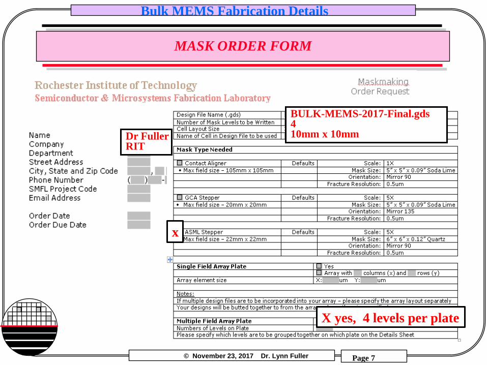
MASK ORDER FORM
x
BULK-MEMS-2017-Final.gds 410mm x 10mmDr Fuller
RIT
X yes, 4 levels per plate

© November 23, 2017 Dr. Lynn Fuller
Bulk MEMS Fabrication Details
Page 8
Rochester Institute of Technology
Microelectronic Engineering
MASK ORDER FORM DETAILS
Layer Reticle
Name
Design .gds
Layer #’s
Boolean Function Dark/
Clear
Comment
1st Diffusion 1 1 Inverted Dark Mirror
2nd Cut 6 6 Inverted Dark Mirror
3rd Metal 7 None Clear Mirror
4th Hole 4 4 Inverted Dark No mirror
Hole pattern is put on the back side of the wafer so it does not get mirrored. All the other layers are mirrored.
Design Layer 9 Out (outline) is not used. It is only for placement of projects on the multi-project reticle template.

© November 23, 2017 Dr. Lynn Fuller
Bulk MEMS Fabrication Details
Page 9
Rochester Institute of Technology
Microelectronic Engineering
LAYER 1 DIFFUSION AND LAYER 2 CUT
CUT
.gds #6
DIFFUSION
.gds #1

© November 23, 2017 Dr. Lynn Fuller
Bulk MEMS Fabrication Details
Page 10
Rochester Institute of Technology
Microelectronic Engineering
LAYER 3 METAL AND LAYER 4 BACKSIDE HOLE
BACKSIDE HOLE
.gds #4
METAL
.gds #7

© November 23, 2017 Dr. Lynn Fuller
Bulk MEMS Fabrication Details
Page 11
Rochester Institute of Technology
Microelectronic Engineering
BULK MEMS PROCESS FLOW
15. ET07 - Resist Strip, Solvent Strip16. CL01 – RCA Clean two HF dips17. Sputter metal 1um, 30min18. PH03 – level 3 Metal19. ET55 – Metal Etch – wet20. Strip Resist – Solvent Strip21. Sinter wafers22. PH03 – level 4 Back Hole
+Hand Coat Front with PR+oven bake
23. Etch Oxide in Holes on Back Wet 24. STS Etch Silicon from Back25. TE01 – wafer level testing26. SAW1– Saw wafers 27. Packaging and Testing28. Documentation
11-20-17
1. Starting wafer, 10um SOI2. Grow 5000Å oxide, Recipe 3503. PH03 – level 0, Marks4. ET06 – Wet Etch Alignment Marks5. Strip resist and clean6. Grow another 5000Å oxide, Recipe 3507. PH03 – level 1 Diffusion
+ Hand Coat back of wafer with PR+ oven bake
8. ET06 –Wet Etch Oxide9. ET07 – Resist Strip, Solvent Strip10. CL01- RCA Clean 11. IM01 - Implant 1E15, B11, Energy 80Kev12. OX05 – 3000Å Dry Oxide, Anneal13. PH03 – level 2 Contact Cut
+ Hand coat back of wafer with PR+ oven bake
14. ET29 – Etch CC Oxide

© November 23, 2017 Dr. Lynn Fuller
Bulk MEMS Fabrication Details
Page 12
Rochester Institute of Technology
Microelectronic Engineering
GENERIC DEVICE CROSS SECTION
Diffusion (Green) Layer 1Backside Hole (Purple Outline) Layer 4Contact Cut (White) Layer 6Metal (Blue) Layer 7Outline (Yellow Outline) Layer 9
Outline is only for layout, drawing a 4.5mm by 4.5mm outline, the maximum area for individual device designs .
p - typen - type
1 um BOX
10um
500um
© November 23, 2017 Dr. Lynn Fuller
Bulk MEMS Fabrication Details
Page 13
Rochester Institute of Technology
Microelectronic Engineering
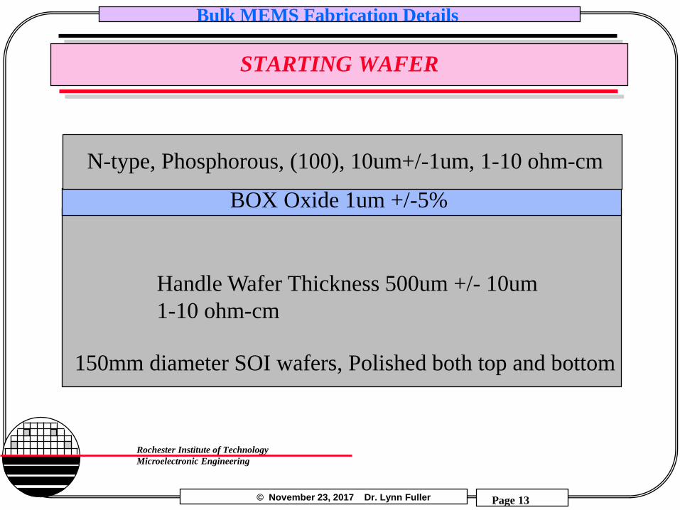
STARTING WAFER
Handle Wafer Thickness 500um +/- 10um
1-10 ohm-cm
150mm diameter SOI wafers, Polished both top and bottom
N-type, Phosphorous, (100), 10um+/-1um, 1-10 ohm-cm
BOX Oxide 1um +/-5%

© November 23, 2017 Dr. Lynn Fuller
Bulk MEMS Fabrication Details
Page 14
Rochester Institute of Technology
Microelectronic Engineering
SSI COAT AND DEVELOP TRACK FOR 6” WAFERS
Use Recipe: COAT.rcp and DEVELOP.rcp
© November 23, 2017 Dr. Lynn Fuller
Bulk MEMS Fabrication Details
Page 15
Rochester Institute of Technology
Microelectronic Engineering
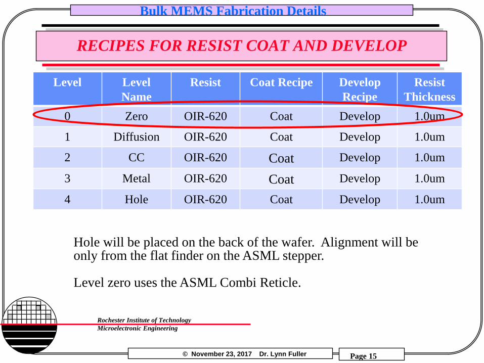
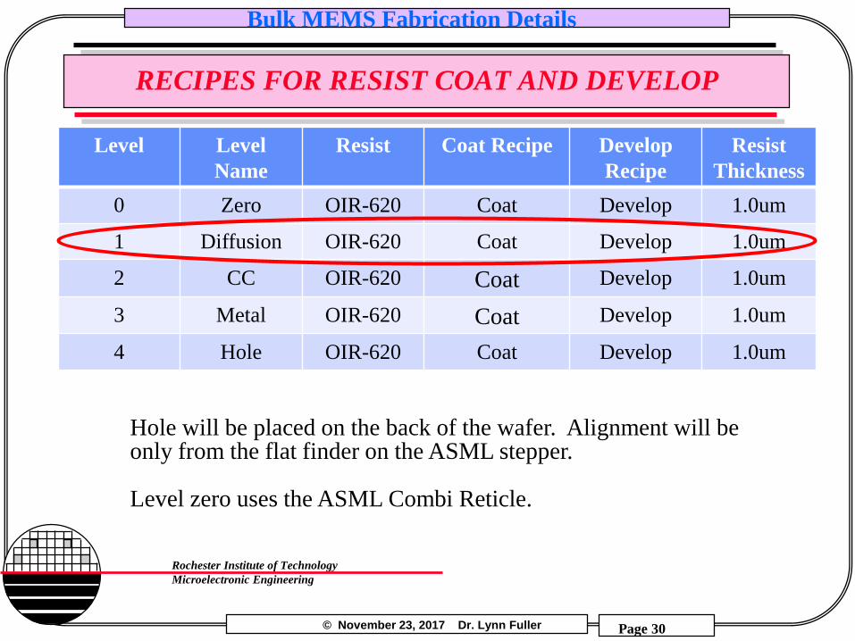
RECIPES FOR RESIST COAT AND DEVELOP
Level Level
Name
Resist Coat Recipe Develop
Recipe
Resist
Thickness
0 Zero OIR-620 Coat Develop 1.0um
1 Diffusion OIR-620 Coat Develop 1.0um
2 CC OIR-620 Coat Develop 1.0um
3 Metal OIR-620 Coat Develop 1.0um
4 Hole OIR-620 Coat Develop 1.0um
Hole will be placed on the back of the wafer. Alignment will be only from the flat finder on the ASML stepper.
Level zero uses the ASML Combi Reticle.

© November 23, 2017 Dr. Lynn Fuller
Bulk MEMS Fabrication Details
Page 16
Rochester Institute of Technology
Microelectronic Engineering
PHOTORESIST PROCESSING
SPIN COAT
OIR 620-10
Resist
3250rpm, 30 sec.
SOFT BAKE
90 °C
60 sec.
DEHYDRATE BAKE/
HMDS PRIMING
HMDS Vapor
Prime
140 °C, 60 sec.
DEVELOP.RCP
POST EXPOSURE BAKE
110 °C, 60 sec.
HARD BAKE
120 °C, 60 sec.
COAT.RCP
DEVELOP
DI Wet
CD-26 Developer
48sec. Puddle,
30sec. Rinse,
30sec., 3750rpm
Spin Dry

© November 23, 2017 Dr. Lynn Fuller
Bulk MEMS Fabrication Details
Page 17
Rochester Institute of Technology
Microelectronic Engineering
ASML 5500/200
NA = 0.48 to 0.60 variable= 0.35 to 0.85 variable
With Variable Kohler, orVariable Annular illuminationResolution = K1 l/NA
= ~ 0.35µm for NA=0.6, =0.85
Depth of Focus = k2 l/(NA)2
= 1.0 µm for NA = 0.6i-Line Stepper l = 365 nm
22 x 27 mm Field Size
© November 23, 2017 Dr. Lynn Fuller
Bulk MEMS Fabrication Details
Page 18
Rochester Institute of Technology
Microelectronic Engineering
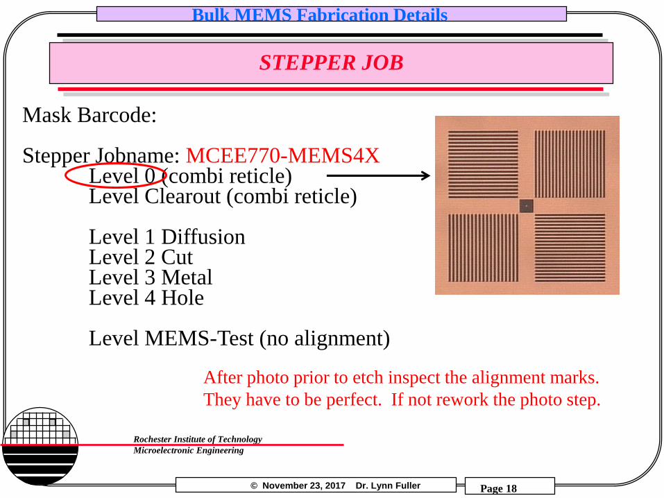
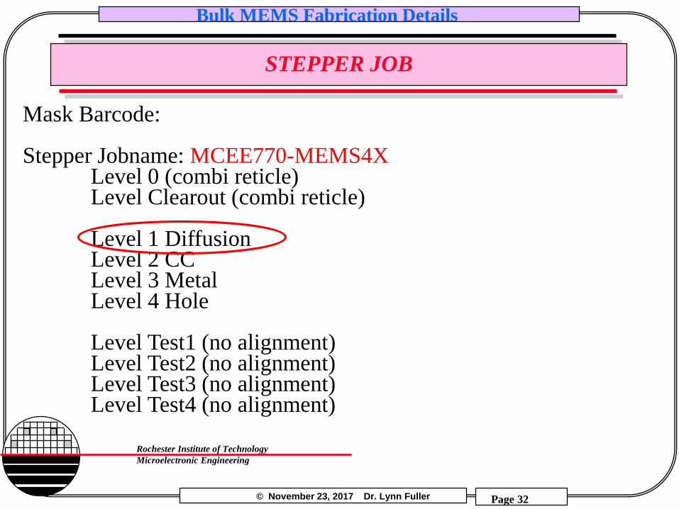
STEPPER JOB
Mask Barcode:
Stepper Jobname: MCEE770-MEMS4XLevel 0 (combi reticle)Level Clearout (combi reticle)
Level 1 DiffusionLevel 2 CutLevel 3 Metal Level 4 Hole
Level MEMS-Test (no alignment)
After photo prior to etch inspect the alignment marks.
They have to be perfect. If not rework the photo step.
© November 23, 2017 Dr. Lynn Fuller
Bulk MEMS Fabrication Details
Page 19
Rochester Institute of Technology
Microelectronic Engineering
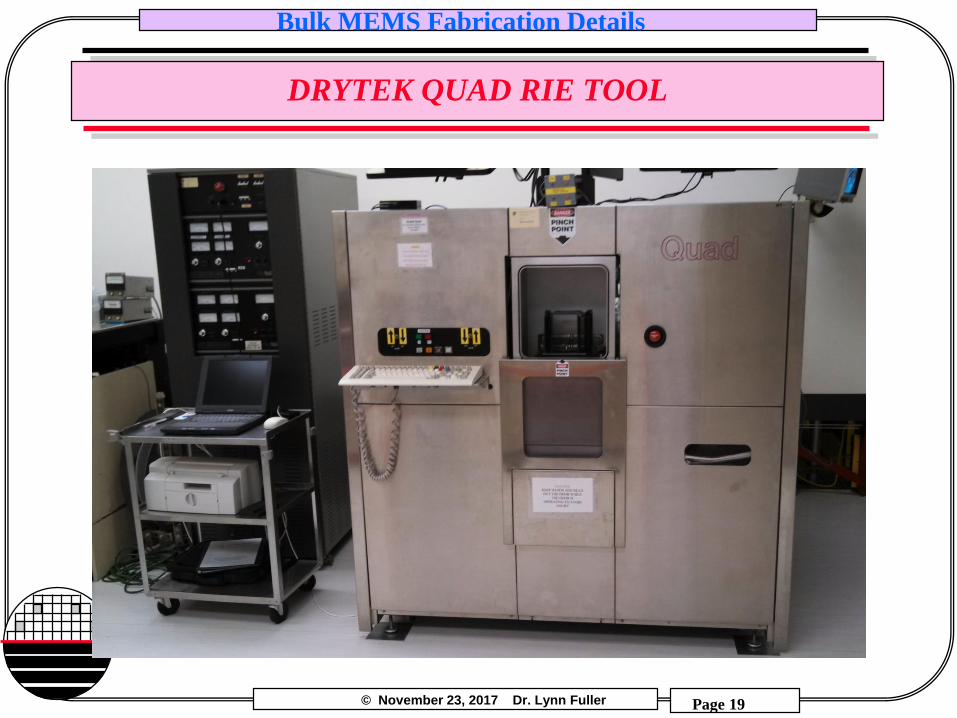
DRYTEK QUAD RIE TOOL

© November 23, 2017 Dr. Lynn Fuller
Bulk MEMS Fabrication Details
Page 20
Rochester Institute of Technology
Microelectronic Engineering
ZERO ETCH FOR ASML ALIGNMENT MARKS
Recipe Name: ZEROETCHChamber 3Power 200WPressure 100 mTorrGas 1 CHF3 50 sccmGas 2 CF4 25 sccmGas 3 Ar 0 sccmGas 4 O2 10 sccm
Max Time = 120 seconds
Silicon Etch Rate 650 Å/min 8.8 um L/S 8 um L/S

© November 23, 2017 Dr. Lynn Fuller
Bulk MEMS Fabrication Details
Page 21
Rochester Institute of Technology
Microelectronic Engineering
SCRIBE WAFER WITH ID NUMBER
Wafer has alignment marks etched in two locations.
Scribe on back of wafer
near the wafer flat
ID numbers D1, D2…etc.
D1
FrontBack

© November 23, 2017 Dr. Lynn Fuller
Bulk MEMS Fabrication Details
Page 22
Rochester Institute of Technology
Microelectronic Engineering
ASHER, SCRIBE, RCA CLEAN & SRD
Gassonics Asher
Recipe FF
RCA Clean Bench
O2 + Energy = 2 OO is reactive and will combinewith plastics, wood, carbon,
photoresist, etc.

© November 23, 2017 Dr. Lynn Fuller
Bulk MEMS Fabrication Details
Page 23
Rochester Institute of Technology
Microelectronic Engineering
RCA CLEAN
DI waterrinse, 5 min.
H20 - 50HF - 130 sec.
HPMHCL - 1part
H2O2 - 1partsH2O - 17parts70 °C, 15 min.
SPIN/RINSEDRY
APMNH4OH - 1partH2O2 - 1partsH2O - 17parts70 °C, 15 min.
DI waterrinse, 5 min.
DI waterrinse, 5 min.

© November 23, 2017 Dr. Lynn Fuller
Bulk MEMS Fabrication Details
Page 24
Rochester Institute of Technology
Microelectronic Engineering
USING EXCEL SPREADSHEET FOR OXIDE GROWTH CALCULATIONS
These spreadsheets are available on Dr. Fullers webpage.

© November 23, 2017 Dr. Lynn Fuller
Bulk MEMS Fabrication Details
Page 25
Rochester Institute of Technology
Microelectronic Engineering
BRUCE FURNACE RECIPE 406 – WET OXIDE 6,500Å
1100°C
800 °C
Boat Out Boat In Boat Out
Load Push Stabilize Ramp-Up Soak Anneal Ramp-Down Pull
Recipe #406
800 °C
25 °C
Any
0 lpm
none
800 °C
At the end of a run the furnace returns to Interval 0 which is set for boat out, 25 °C and no gas flow. The furnace waits in that state until someone aborts the current recipe or loads a new recipe.
Wet Oxide Growth, Target 6,500 Å, Tube 1
Interval 0 Interval 1 Interval 2 Interval 3 Interval 4 Interval 5 Interval 6 Interval 7 Interval 8
12 min 15 min 30 min 5 min 65 min 5 min 60 min 12 min
10 lpm 10 lpm 5 lpm 5 lpm 3.6/2 lpm 15 lpm 10 lpm 15 lpm
N2 N2 N2 O2 O2/H2 N2 N2 N2
© November 23, 2017 Dr. Lynn Fuller
Bulk MEMS Fabrication Details
Page 26
Rochester Institute of Technology
Microelectronic Engineering
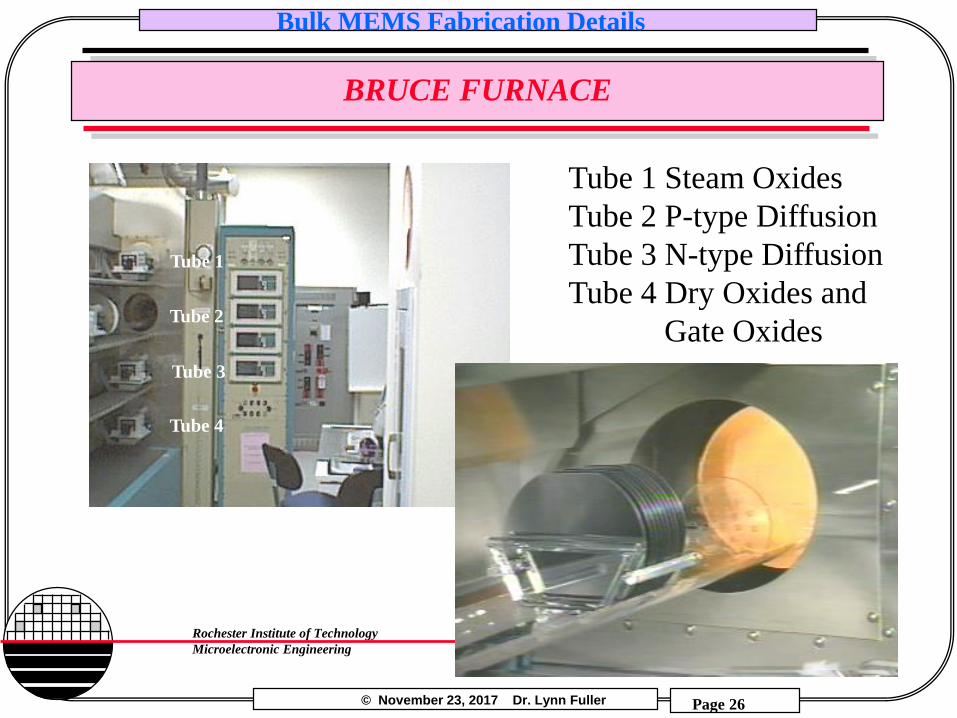
BRUCE FURNACE
Tube 1 Steam Oxides
Tube 2 P-type Diffusion
Tube 3 N-type Diffusion
Tube 4 Dry Oxides and
Gate Oxides
Tube 1
Tube 2
Tube 3
Tube 4

© November 23, 2017 Dr. Lynn Fuller
Bulk MEMS Fabrication Details
Page 27
Rochester Institute of Technology
Microelectronic Engineering
TENCORE FT-300 SPECROMAP
Record:
Mean
Std Deviation
Min
Max
No of Points

© November 23, 2017 Dr. Lynn Fuller
Bulk MEMS Fabrication Details
Page 28
Rochester Institute of Technology
Microelectronic Engineering
AFTER 6500Å OXIDE GROWTH
Starting Wafer
6500 Å

© November 23, 2017 Dr. Lynn Fuller
Bulk MEMS Fabrication Details
Page 29
Rochester Institute of Technology
Microelectronic Engineering
SSI COAT AND DEVELOP TRACK FOR 6” WAFERS
Use Recipe: Coat.rcp and Develop.rcp
© November 23, 2017 Dr. Lynn Fuller
Bulk MEMS Fabrication Details
Page 30
Rochester Institute of Technology
Microelectronic Engineering
RECIPES FOR RESIST COAT AND DEVELOP
Level Level
Name
Resist Coat Recipe Develop
Recipe
Resist
Thickness
0 Zero OIR-620 Coat Develop 1.0um
1 Diffusion OIR-620 Coat Develop 1.0um
2 CC OIR-620 Coat Develop 1.0um
3 Metal OIR-620 Coat Develop 1.0um
4 Hole OIR-620 Coat Develop 1.0um
Hole will be placed on the back of the wafer. Alignment will be only from the flat finder on the ASML stepper.
Level zero uses the ASML Combi Reticle.

© November 23, 2017 Dr. Lynn Fuller
Bulk MEMS Fabrication Details
Page 31
Rochester Institute of Technology
Microelectronic Engineering
ASML 5500/200
NA = 0.48 to 0.60 variable= 0.35 to 0.85 variable
With Variable Kohler, orVariable Annular illuminationResolution = K1 l/NA
= ~ 0.35µm for NA=0.6, =0.85
Depth of Focus = k2 l/(NA)2
= 1.0 µm for NA = 0.6i-Line Stepper l = 365 nm
22 x 27 mm Field Size
© November 23, 2017 Dr. Lynn Fuller
Bulk MEMS Fabrication Details
Page 32
Rochester Institute of Technology
Microelectronic Engineering
STEPPER JOB
Mask Barcode:
Stepper Jobname: MCEE770-MEMS4XLevel 0 (combi reticle)Level Clearout (combi reticle)
Level 1 DiffusionLevel 2 CCLevel 3 MetalLevel 4 Hole
Level Test1 (no alignment)Level Test2 (no alignment)Level Test3 (no alignment)Level Test4 (no alignment)

© November 23, 2017 Dr. Lynn Fuller
Bulk MEMS Fabrication Details
Page 33
Rochester Institute of Technology
Microelectronic Engineering
AFTER PHOTORESIST COAT, EXPOSE & DEVELOP

© November 23, 2017 Dr. Lynn Fuller
Bulk MEMS Fabrication Details
Page 34
Rochester Institute of Technology
Microelectronic Engineering
AFTER OXIDE ETCH

© November 23, 2017 Dr. Lynn Fuller
Bulk MEMS Fabrication Details
Page 35
Rochester Institute of Technology
Microelectronic Engineering
STRIP RESIST, RCA CLEAN

© November 23, 2017 Dr. Lynn Fuller
Bulk MEMS Fabrication Details
Page 36
Rochester Institute of Technology
Microelectronic Engineering
ION IMPLANT BORON
Ion Implant B11Dose = 1E15 cm-2Energy = 100KeVTime ~10min at 100 µA

© November 23, 2017 Dr. Lynn Fuller
Bulk MEMS Fabrication Details
Page 37
Rochester Institute of Technology
Microelectronic Engineering
IMPLANT MASKING THICKNESS CALCULATOR

© November 23, 2017 Dr. Lynn Fuller
Bulk MEMS Fabrication Details
Page 38
Rochester Institute of Technology
Microelectronic Engineering
AFTER ION IMPLANT BORON
Ion Implant B11Dose = 1E15 cm-2Energy = 100KeVTime ~10min at 100 µA

© November 23, 2017 Dr. Lynn Fuller
Bulk MEMS Fabrication Details
Page 39
Rochester Institute of Technology
Microelectronic Engineering
ANNEAL, DIFFUSION, OXIDE GROWTH

© November 23, 2017 Dr. Lynn Fuller
Bulk MEMS Fabrication Details
Page 40
Rochester Institute of Technology
Microelectronic Engineering
BRUCE FURNACE RECIPE 341 – WET OXIDE 4,000Å
1000°C
800 °C
Boat Out Boat In Boat Out
Load Push Stabilize Ramp-Up Flood Soak Anneal Ramp-Down Pull
12 min 15 min 20 min 5 min 20 min 5 min 40 min 12 min
10 lpm 10 lpm 5 lpm 5 lpm 10 lpm 15 lpm 10 lpm 15 lpm
N2 N2 N2 O2 O2/H2 N2 N2 N2
Recipe #341
Interval 0 Interval 1 Interval 2 Interval 3 Interval 4 Interval 5 Interval 6 Interval 7 Interval 8
800 °C
25 °C
Any
0 lpm
none
800 °C
At the end of a run the furnace returns to Interval 0 which is set for boat out, 25 °C and no gas flow. The furnace waits in that state until someone aborts the current recipe or loads a new recipe.
Wet Oxide Growth, Target 4000 Å

© November 23, 2017 Dr. Lynn Fuller
Bulk MEMS Fabrication Details
Page 41
Rochester Institute of Technology
Microelectronic Engineering
RECIPES FOR RESIST COAT AND DEVELOP
Level Level
Name
Resist Coat Recipe Develop
Recipe
Resist
Thickness
0 Zero OIR-620 Coat Develop 1.0um
1 Diffusion OIR-620 Coat Develop 1.0um
2 CC OIR-620 Coat Develop 1.0um
3 Metal OIR-620 Coat Develop 1.0um
4 Hole OIR-620 Coat Develop 1.0um
Hole will be placed on the back of the wafer. Alignment will be only from the flat finder on the ASML stepper.
Level zero uses the ASML Combi Reticle.

© November 23, 2017 Dr. Lynn Fuller
Bulk MEMS Fabrication Details
Page 42
Rochester Institute of Technology
Microelectronic Engineering
AFTER CONTACT CUT ETCH AND RESIST STRIP

© November 23, 2017 Dr. Lynn Fuller
Bulk MEMS Fabrication Details
Page 43
Rochester Institute of Technology
Microelectronic Engineering
PRE METAL HF DIP
SPIN/RINSEDRY
H20 - 50HF - 130 sec.
DI waterrinse, 5 min.

© November 23, 2017 Dr. Lynn Fuller
Bulk MEMS Fabrication Details
Page 44
Rochester Institute of Technology
Microelectronic Engineering
AFTER METAL DEPOSITION
CVC 601 Sputter Tool
Pressure = 5mTorr
Power = 2000 Watts
Time = 30 min
Thickness = ~ 1.0um

© November 23, 2017 Dr. Lynn Fuller
Bulk MEMS Fabrication Details
Page 45
Rochester Institute of Technology
Microelectronic Engineering
SPUTTER ALUMINUM
CVC 601 Sputter Tool
Pressure = 5mTorr
Power = 2000 Watts
Time = 30 min
Thickness = ~ 1.0um

© November 23, 2017 Dr. Lynn Fuller
Bulk MEMS Fabrication Details
Page 46
Rochester Institute of Technology
Microelectronic Engineering
RECIPES FOR RESIST COAT AND DEVELOP
Level Level
Name
Resist Coat Recipe Develop
Recipe
Resist
Thickness
0 Zero OIR-620 Coat Develop 1.0um
1 Diffusion OIR-620 Coat Develop 1.0um
2 CC OIR-620 Coat Develop 1.0um
3 Metal OIR-620 Coat Develop 1.0um
4 Hole OIR-620 Coat Develop 1.0um
Hole will be placed on the back of the wafer. Alignment will be only from the flat finder on the ASML stepper.
Level zero uses the ASML Combi Reticle.

© November 23, 2017 Dr. Lynn Fuller
Bulk MEMS Fabrication Details
Page 47
Rochester Institute of Technology
Microelectronic Engineering
METAL PHOTO
© November 23, 2017 Dr. Lynn Fuller
Bulk MEMS Fabrication Details
Page 48
Rochester Institute of Technology
Microelectronic Engineering
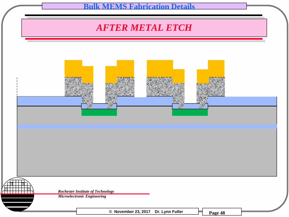
AFTER METAL ETCH
© November 23, 2017 Dr. Lynn Fuller
Bulk MEMS Fabrication Details
Page 49
Rochester Institute of Technology
Microelectronic Engineering
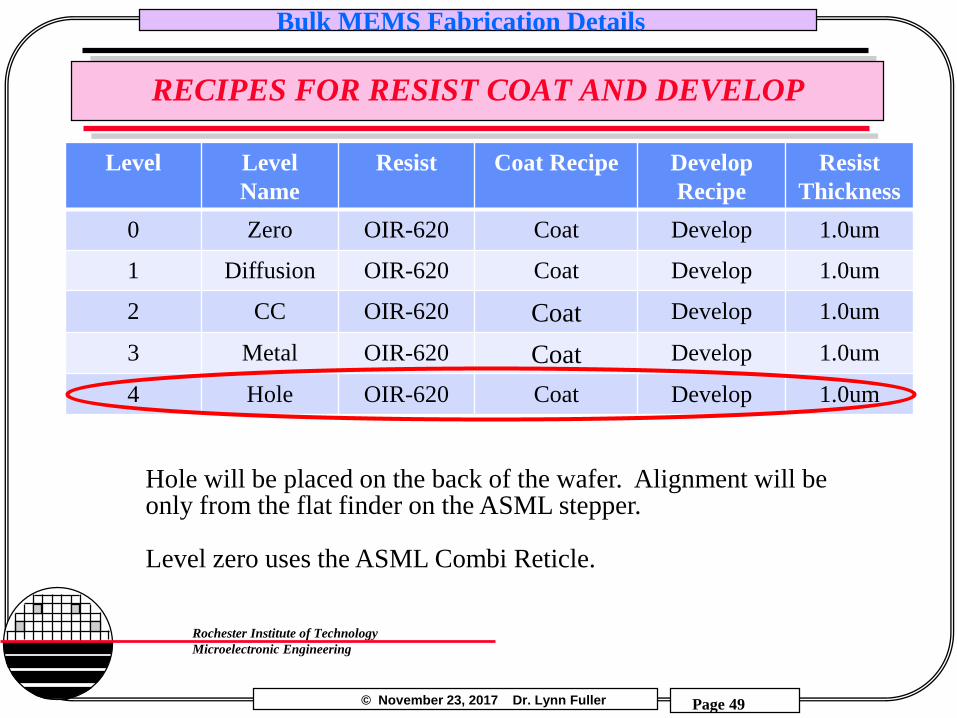
RECIPES FOR RESIST COAT AND DEVELOP
Level Level
Name
Resist Coat Recipe Develop
Recipe
Resist
Thickness
0 Zero OIR-620 Coat Develop 1.0um
1 Diffusion OIR-620 Coat Develop 1.0um
2 CC OIR-620 Coat Develop 1.0um
3 Metal OIR-620 Coat Develop 1.0um
4 Hole OIR-620 Coat Develop 1.0um
Hole will be placed on the back of the wafer. Alignment will be only from the flat finder on the ASML stepper.
Level zero uses the ASML Combi Reticle.

© November 23, 2017 Dr. Lynn Fuller
Bulk MEMS Fabrication Details
Page 50
Rochester Institute of Technology
Microelectronic Engineering
HOLE PHOTO

© November 23, 2017 Dr. Lynn Fuller
Bulk MEMS Fabrication Details
Page 51
Rochester Institute of Technology
Microelectronic Engineering
BOSCH ICP (PLASMA THERM)
Deep Reactive Ion Etch (DRIE) The Bosch process uses two chemistries, one to generate polymers and the other to etch silicon. The etch machine switches between the two every few seconds to ensure that the sidewalls are covered with polymer allowing fast, deep trench etching. (the substrate is on a chuck that is cooled by liquid nitrogen.
•5µm spaces
•200µm etch depth
•40:1 aspect ratio
•2µm/min Si etch rate
•>75:1 selectivity to
photoresist

© November 23, 2017 Dr. Lynn Fuller
Bulk MEMS Fabrication Details
Page 52
Rochester Institute of Technology
Microelectronic Engineering
STS ETCH TOOL AT RIT
Deep Reactive Ion Etch (DRIE)
© November 23, 2017 Dr. Lynn Fuller
Bulk MEMS Fabrication Details
Page 53
Rochester Institute of Technology
Microelectronic Engineering
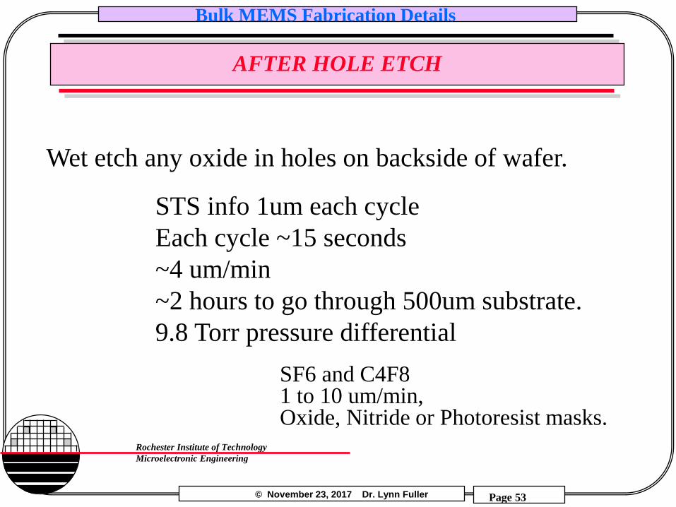
AFTER HOLE ETCH
STS info 1um each cycle
Each cycle ~15 seconds
~4 um/min
~2 hours to go through 500um substrate.
9.8 Torr pressure differential
Wet etch any oxide in holes on backside of wafer.
SF6 and C4F81 to 10 um/min, Oxide, Nitride or Photoresist masks.

© November 23, 2017 Dr. Lynn Fuller
Bulk MEMS Fabrication Details
Page 54
Rochester Institute of Technology
Microelectronic Engineering
AFTER HOLE ETCH

© November 23, 2017 Dr. Lynn Fuller
Bulk MEMS Fabrication Details
Page 55
Rochester Institute of Technology
Microelectronic Engineering
TEST EQUIPMENT
Manual Prober

© November 23, 2017 Dr. Lynn Fuller
Bulk MEMS Fabrication Details
Page 56
Rochester Institute of Technology
Microelectronic Engineering
K&S 780 WAFER SAW

© November 23, 2017 Dr. Lynn Fuller
Bulk MEMS Fabrication Details
Page 57
Rochester Institute of Technology
Microelectronic Engineering
AFTER SAWING AND REMOVAL OF GOOD CHIPS
Wafer Sawing Movie

© November 23, 2017 Dr. Lynn Fuller
Bulk MEMS Fabrication Details
Page 58
Rochester Institute of Technology
Microelectronic Engineering
RIT PACKAGED PRESSURE SENSOR

© November 23, 2017 Dr. Lynn Fuller
Bulk MEMS Fabrication Details
Page 59
Rochester Institute of Technology
Microelectronic Engineering
ULTRASONIC ALUMINUM WIREBOND
Bond 1, time=1, power=250Bond 2, time=2, power=320 Orthodyne Electronics Model 20
Ultrasonic Wire Bonder
© November 23, 2017 Dr. Lynn Fuller
Bulk MEMS Fabrication Details
Page 60
Rochester Institute of Technology
Microelectronic Engineering
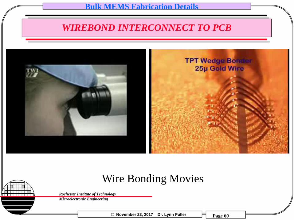
WIREBOND INTERCONNECT TO PCB
Wire Bonding Movies

© November 23, 2017 Dr. Lynn Fuller
Bulk MEMS Fabrication Details
Page 61
Rochester Institute of Technology
Microelectronic Engineering
SUMMARY
This project allows students to see the entire process for design, fabrication, packaging and testing of a MEMS based Microsystem.

© November 23, 2017 Dr. Lynn Fuller
Bulk MEMS Fabrication Details
Page 62
Rochester Institute of Technology
Microelectronic Engineering
REFERENCES
1. Dr. Lynn Fuller’s webpage2. more
© November 23, 2017 Dr. Lynn Fuller
Bulk MEMS Fabrication Details
Page 63
Rochester Institute of Technology
Microelectronic Engineering
HOMEWORK – BULK FABRICATION DETAILS
1. Draw a series of pictures that show the crossection of a
pressure sensor after step 12, 16, 19 and 24.