Embed Size (px)
Citation preview

Building a PA Design Framework for 5G Applications

© 2020 Cadence Design Systems, Inc. All rights reserved.2
Focus Areas
• Cadence® AWR® Visual System Simulator™ (VSS) software brief introduction
• Amplifier modeling capabilities in VSS software
• Overview of 5G and unique challenges to power amplifier (PA) design
• Phased arrays for 5G systems
• VSS 5G testbenches for PA design and analysis

© 2020 Cadence Design Systems, Inc. All rights reserved.3
VSS Software
• Toolset for designing and analyzing from simple RF links to complete RF systems
o Part of Cadence® AWR Design Environment® software
o Powerful RF link design and analysis capabilities
o Modeling and evaluation of complete communications and radar systems
• VSS top-level capabilities:
o RF budget analysis, RF spur heritage
o Time-domain simulations: spectrum, error vector magnitude (EVM), adjacent channel power ratio (ACPR), bit error rate (BER), throughput, etc.
o Phased array design, standard communication libraries
Channel and EnvironmentalRF (Analog)Baseband(Digital)
TX RF Link
RX RF Link
TX Signal
Generation
RX Signal
Processing
Antenna Channel
VSS includes
models for every
component in such
systems!

© 2020 Cadence Design Systems, Inc. All rights reserved.4
VSS Software for RF System Simulation
The most complete RF system
simulation functionality in one
integrated tool
RF Budget (RFB)Cascaded gain,input/output IP3,noise figure, etc.
RF Inspector (RFI)Heritage tone inspector to identify the cause of an
inter-modulation product of an RF link
Time DomainEnd-to-end analysis
C/N, BER, ACPR, EVM, etc.
Circuit co-simulationMATLAB/LabVIEW co-sim,Communication standardsWiMAX, WCDMA, LTE, GSM EDGE,
DVB, 802.11a/b/g/n/ac
HW-in-loop simulations
RFB, RFI, and time-domain simulators
use the same RF link design!

© 2020 Cadence Design Systems, Inc. All rights reserved.5
BPFBID=F1LOSS=0 dBN=3FP1=900 MHzFP2=1100 MHzAP=0.1 dBNOISE=Auto
AMP_BID=A2GAIN=10 dBP1DB=10 dBmIP3= IP2=
MEASREF= OPSAT= NF=3 dBNOISE=AutoRFIFRQ=
BPFBID=F2LOSS=0 dBN=N1FP1=900 MHzFP2=1100 MHzAP=0.1 dBNOISE=Auto
ISOLATORID=S1LOSS=0 dBISOL=30 dBNOISE=AutoZINP=_Z0 OhmZOUTP=_Z0 Ohm
IN OUT
LO
MIXER_BID=A3MODE=ModeLOMULT=1FCOUT= RFIFRQ={ 100,1200 } MHzGCONV=-6 dBP1DB=10 dBm
IP3=30 dBmLO2OUT=-25 dBIN2OUT=-20 dBLO2IN=-25 dBOUT2IN=-25 dBPLO= PLOUSE=Spur reference onlyPIN=
PINUSE=IN2OUTH OnlyNF=6 dBNOISE=Auto
LPFBID=F3LOSS=0 dBN=4FP=500 MHzNOISE=Auto
TONEID=A4FRQ=1200 MHzPWR=10 dBmPHS=0 DegCTRFRQ=
SMPFRQ= ZS=_Z0 OhmTN=_TAMB DegKNOISE=AutoPNMASK= PNOISE=No phase noise
TPID=Start
TPID=Stop
M_PROBEID=MP1
PORT_SRCP=1ZS=_Z0 OhmSignal=SinusoidSpecType=Use doc freqSpecBW=Specify freq spanSweep=NoneSpan=1000 MHzPwr=-10 dBmAng=0 Deg
PORTP=2Z=_Z0 Ohm
Effect of filter order on NF or gain at
image frequency measurements?
How can I reduce my spur levels?
RFB and RFI
RFB and RFI support:
• Optimization and yield analysis
• Impedance mismatch
• Frequency and temperature dependency
Xo Xn. . .
SWPVARID=SWP1VARNAME="N1"VALUES=swpstp(3,7,1)VALTYPE=ScalarUNITUSE=Project UnitsSWPDUR= SWPCNT=
• Frequency domain circuit solver
• Use RFB to surpass capabilities of common spread sheet and provide greater insight on RF architecture
• Use RFI to identify and mitigate unwanted spurs

© 2020 Cadence Design Systems, Inc. All rights reserved.6
Time-Domain System Simulation
• Use the same RF link design as RFB and RFI
• Drive it with modulated signals and perform a wide variety of measurements
QAM_SRCID=A1MOD=16-QAM (Gray)OUTLVL=-10OLVLTYP=Avg. Power (dBm)RATE=2e6
CTRFRQ=1000 MHzPLSTYP=Root Raised CosineALPHA=0.35PLSLN= SMPSYM=_SMPSYM
TPID=DUT_IN
TPID=DUT_OUT
R D
IQ
1 2
3
45
RCVRID=A3
R D
IQ
1 2
3
45
QAM_RXID=A2
TPID=DEM
TPID=REF
DUT
SUBCKTID=S2NET="RF Link"Mode=DIFF
Modulated Signal Test Bench
BPFBID=F1LOSS=0 dBN=3FP1=900 MHzFP2=1100 MHzAP=0.1 dBNOISE=Auto
AMP_BID=A2GAIN=10 dBP1DB=10 dBmIP3= IP2=
MEASREF= OPSAT= NF=3 dBNOISE=AutoRFIFRQ=
BPFBID=F2LOSS=0 dBN=N1FP1=900 MHzFP2=1100 MHzAP=0.1 dBNOISE=Auto
ISOLATORID=S1LOSS=0 dBISOL=30 dBNOISE=AutoZINP=_Z0 OhmZOUTP=_Z0 Ohm
IN OUT
LO
MIXER_BID=A3MODE=ModeLOMULT=1FCOUT= RFIFRQ={ 100,1200 } MHzGCONV=-6 dBP1DB=10 dBm
IP3=30 dBmLO2OUT=-25 dBIN2OUT=-20 dBLO2IN=-25 dBOUT2IN=-25 dBPLO= PLOUSE=Spur reference onlyPIN=
PINUSE=IN2OUTH OnlyNF=6 dBNOISE=Auto
LPFBID=F3LOSS=0 dBN=4FP=500 MHzNOISE=Auto
TONEID=A4FRQ=1200 MHzPWR=10 dBmPHS=0 DegCTRFRQ=
SMPFRQ= ZS=_Z0 OhmTN=_TAMB DegKNOISE=AutoPNMASK= PNOISE=No phase noise
TPID=Start
TPID=Stop
M_PROBEID=MP1
PORT_SRCP=1ZS=_Z0 OhmSignal=SinusoidSpecType=Use doc freqSpecBW=Specify freq spanSweep=NoneSpan=1000 MHzPwr=-10 dBmAng=0 Deg
PORTP=2Z=_Z0 Ohm

© 2020 Cadence Design Systems, Inc. All rights reserved.7
Communication Standard Testbenches
BPFBID=F1LOSS=0 dBN=3FP1=900 MHzFP2=1100 MHzAP=0.1 dBNOISE=Auto
AMP_BID=A2GAIN=10 dBP1DB=10 dBmIP3= IP2=
MEASREF= OPSAT= NF=3 dBNOISE=AutoRFIFRQ=
BPFBID=F2LOSS=0 dBN=N1FP1=900 MHzFP2=1100 MHzAP=0.1 dBNOISE=Auto
ISOLATORID=S1LOSS=0 dBISOL=30 dBNOISE=AutoZINP=_Z0 OhmZOUTP=_Z0 Ohm
IN OUT
LO
MIXER_BID=A3MODE=ModeLOMULT=1FCOUT= RFIFRQ={ 100,1200 } MHzGCONV=-6 dBP1DB=10 dBm
IP3=30 dBmLO2OUT=-25 dBIN2OUT=-20 dBLO2IN=-25 dBOUT2IN=-25 dBPLO= PLOUSE=Spur reference onlyPIN=
PINUSE=IN2OUTH OnlyNF=6 dBNOISE=Auto
LPFBID=F3LOSS=0 dBN=4FP=500 MHzNOISE=Auto
TONEID=A4FRQ=1200 MHzPWR=10 dBmPHS=0 DegCTRFRQ=
SMPFRQ= ZS=_Z0 OhmTN=_TAMB DegKNOISE=AutoPNMASK= PNOISE=No phase noise
TPID=Start
TPID=Stop
M_PROBEID=MP1
PORT_SRCP=1ZS=_Z0 OhmSignal=SinusoidSpecType=Use doc freqSpecBW=Specify freq spanSweep=NoneSpan=1000 MHzPwr=-10 dBmAng=0 Deg
PORTP=2Z=_Z0 Ohm

© 2020 Cadence Design Systems, Inc. All rights reserved.8
VSS RF Models
• Behavioral ( _B )o Configured via gain, P1dB, IP3, noise figure (NF), etc.
o Amp, mixer, OSC, switch, filters, VGA, VVA…
• File based ( _F )o Use measured data
o AM–to–AM/PM, P2D, S-parameters, MDIF
• Circuit simulation based ( _S )o Extract simulation results from AWR® Microwave Office® software, circuit schematics
o LNA, PA, mixer, OSC, filters
RF blocks account for VSWR effects, frequency and temperature
dependency, support yield analysis, and optimization!

© 2020 Cadence Design Systems, Inc. All rights reserved.9
Co-Simulating with Circuit Models
• VSS software offers seamless co-simulation with AWR® Microwave Office®
software, circuit models may be easily included in VSS testbenches
© 2020 Cadence Design Systems, Inc. All rights reserved.10
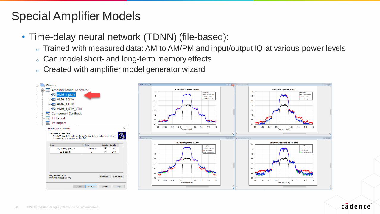
Special Amplifier Models
• Time-delay neural network (TDNN) (file-based):o Trained with measured data: AM to AM/PM and input/output IQ at various power levels
o Can model short- and long-term memory effects
o Created with amplifier model generator wizard

© 2020 Cadence Design Systems, Inc. All rights reserved.11
Special Amplifier Models (cont.)
• Load-pull amplifier models in VSS softwareo Simulate load-pull for EVM and ACPR, build contours for various loading conditions

© 2020 Cadence Design Systems, Inc. All rights reserved.12
DPD Design in VSS Software
• Various digital predistortion (DPD) algorithms supported in VSS software:
o Theoretical algorithms include lookup table (LUT), memory polynomial, generalized memory polynomial, dynamic deviation reduction second order

© 2020 Cadence Design Systems, Inc. All rights reserved.13
5G Overview: Enabling Technologies
• Advanced coding and modulation schemes (part of 5G New Radio [NR] standard)o Improves spectral efficiency
o Requires efficient, linear PAs that can address wider bandwidth and high PAPR
• Use of mmWave spectrumo Provides bandwidth for high data rates
o Requires front-end components (including antennas) that can overcome higher losses at mm-wave frequencies
• Massive multiple-in-multiple-out (MIMO) and beam steering o Enables spatial efficiency, densification
o Requires commercialized phased array antenna systems

© 2020 Cadence Design Systems, Inc. All rights reserved.14
* https://www.ericsson.com/research-blog/in-race-to-5g-cp-ofdm-triumphs/
*
5G Radio Access Evolution

© 2020 Cadence Design Systems, Inc. All rights reserved.15
5G NR Signal Design
• Frequency band options (RAN4)o LTE re-farming bands: 1, 3, 7, 8, 20, 28, 41, 66, 70, 71
o New sub-6GHz bands: 3.3 – 4.2GHz and 4.4 – 4.9GHz
o mmWave bands: 24.25 – 29.5GHz, 31.8 – 33.4GHz, and 37 – 40GHz
• New modulation featureso CP-OFDM modulation scheme with variable subcarrier spacing (SCS): 3.75 – 480kHz
o Component carrier BW:
– Sub-6GHz: min. 5MHz, max. 100MHz
– > 6GHz: min. 50MHz, max. 400MHz
o Carrier aggregation: max. 16 carriers (RAN1), max. 32 carriers (RAN2)
o Modulation: QPSK, 16QAM, 64QAM, 256QAM, 1024QAM; UL support /2-BPSK

© 2020 Cadence Design Systems, Inc. All rights reserved.16
mmWave 5G
• Why cmWave and mmWave?o Large amount of spectrum available
o Support for ultra-fast communications
o Initially used for fixed-wireless/indoor applications
• Increased design challengeso Initial focus on 28GHz and 39GHz bands
o MIMO operation, much larger channel bandwidths, carrier aggregation
o High propagation loss, low signal penetration

© 2020 Cadence Design Systems, Inc. All rights reserved.17
Phased Array Design and Analysis in AWR Software
• Phased arrays have become an integral part of mmWave 5G systems
• AWR Design Environment® software offers a full range of tools to facilitate phased array system design
o VSS software used as a top-level integration platform
o Phased array generator wizard for interactive array design
o VSS software for advanced system analysis
o Circuit simulator for extracting active impedance vs array scan angle
o EM simulator for initial element analysis, as well as full array verification
© 2020 Cadence Design Systems, Inc. All rights reserved.18
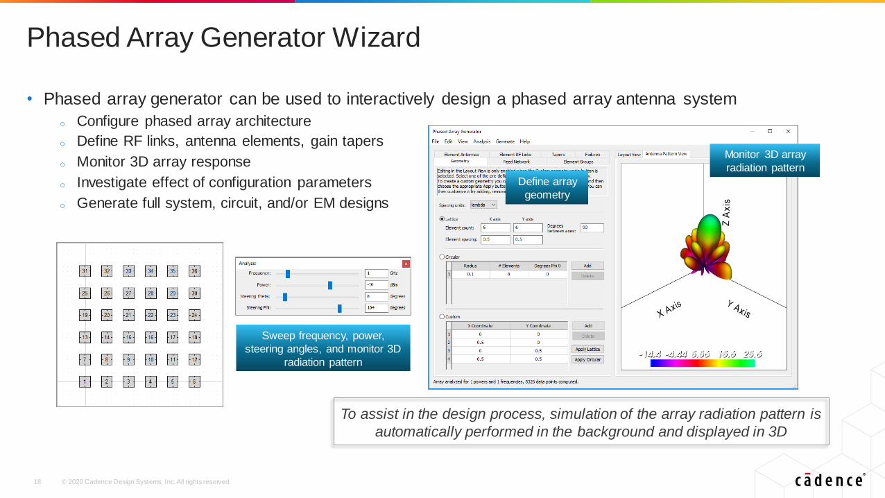
• Phased array generator can be used to interactively design a phased array antenna system
o Configure phased array architecture
o Define RF links, antenna elements, gain tapers
o Monitor 3D array response
o Investigate effect of configuration parameters
o Generate full system, circuit, and/or EM designs
Phased Array Generator Wizard
Monitor 3D array
radiation pattern
Sweep frequency, power,
steering angles, and monitor 3D
radiation pattern
To assist in the design process, simulation of the array radiation pattern is
automatically performed in the background and displayed in 3D
Define array
geometry
© 2020 Cadence Design Systems, Inc. All rights reserved.19
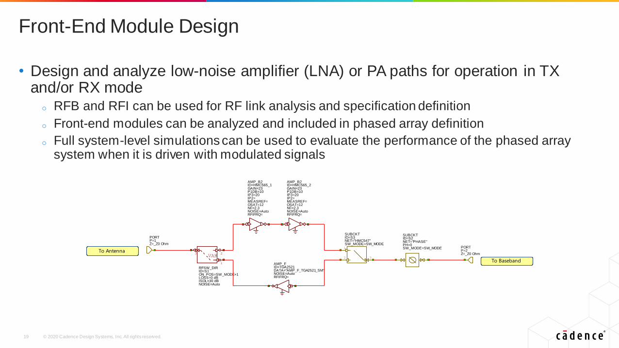
Front-End Module Design
• Design and analyze low-noise amplifier (LNA) or PA paths for operation in TX and/or RX mode
o RFB and RFI can be used for RF link analysis and specification definition
o Front-end modules can be analyzed and included in phased array definition
o Full system-level simulations can be used to evaluate the performance of the phased array system when it is driven with modulated signals
SUBCKTID=S2NET="PHASE"PH=0SW_MODE=SW_MODE PORT
P=2Z=_Z0 Ohm
PORTP=1Z=_Z0 Ohm
AMP_B2ID=HMC565_2GAIN=23P1DB=10IP3=20IP2= MEASREF= OSAT=12NF=2.3NOISE=AutoRFIFRQ=
VAR
1
23
RFSW_DIRID=S1ON_POS=SW_MODE+1LOSS=0 dBISOL=30 dBNOISE=Auto
AMP_B2ID=HMC565_1GAIN=23P1DB=10IP3=20IP2= MEASREF= OSAT=12NF=2.3NOISE=AutoRFIFRQ=
AMP_FID=TGA2521DATA="AMP_F_TGA2521_SM"NOISE=AutoRFIFRQ=
To Antenna
To Baseband
1
2 3
SUBCKTID=S3NET="HMC547"SW_MODE=SW_MODE
© 2020 Cadence Design Systems, Inc. All rights reserved.20
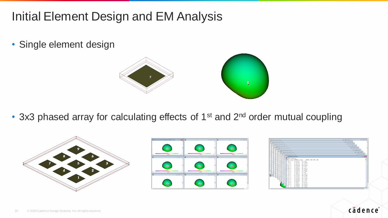
Initial Element Design and EM Analysis
• Single element design
• 3x3 phased array for calculating effects of 1st and 2nd order mutual coupling

© 2020 Cadence Design Systems, Inc. All rights reserved.21
System-Level Models of Phased Array
• The wizard can generate a full system-level model and test bench
o Perform a rigorous analysis in VSS software
o Use the phased array as part of a complete communications or radar system
© 2020 Cadence Design Systems, Inc. All rights reserved.22
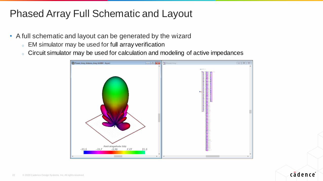
Phased Array Full Schematic and Layout
• A full schematic and layout can be generated by the wizard
o EM simulator may be used for full array verification
o Circuit simulator may be used for calculation and modeling of active impedances

© 2020 Cadence Design Systems, Inc. All rights reserved.23
NR 5G VSS TX Testbenches
• Set up with most common TX measurements, customized according to specification requirements
• Allows users to place their own DUT and start performing measurements in no time

© 2020 Cadence Design Systems, Inc. All rights reserved.24
NR 5G VSS RX Testbenches
• Reference sensitivity analysis, according to specification requirements
• Users can add their own DUT and analyze its impact on system performance

© 2020 Cadence Design Systems, Inc. All rights reserved.25
mmWave 5G VSS Carrier Aggregation Testbenches
• Up to 8 adjacent component carriers, can be spaced as desired and individually enabled or disabled
• 2x2 MIMO implementation available, receiver can demodulate any or all the component carriers

© 2020 Cadence Design Systems, Inc. All rights reserved.26
mmWave 5G Testbench with TX and RX Phased Arrays
• 5G mmWave TX and RX testbenches available in VSS software
o Incorporate baseband signal generation/processing, RF links, phased arrays, and channel propagation
o Phased arrays designed with the phased array generator

© 2020 Cadence Design Systems, Inc. All rights reserved.27
Conclusion
• 5G systems introduce new challenges to amplifier design
• Phased array systems will require much more detailed models and simulations
• VSS software offers a wide range of capabilities to support such challenges:o Accurate amplifier models
o Phased array modeling and design capabilities
o Numerous testbenches to kick-start any design
o Powerful framework for system design and analysis!

© 2020 Cadence Design Systems, Inc. All rights reserved worldwide. Cadence, the Cadence logo, and the other Cadence marks fou nd at www.cadence.com/go/trademarks are trademarks or registered trademarks of Cadence Design
Systems, Inc. Accellera and SystemC are trademarks of Accellera Systems Initiative Inc. All Arm products are registered trademarks or trademarks of Arm Limited (or its subsidiaries) in the US and/or elsewhere. A ll MIPI
specifications are registered trademarks or service marks owned by MIPI Alliance. All PCI-SIG specifications are registered trademarks or trademarks of PCI-SIG. All other trademarks are the property of their respective owners.


![5G End-to-End Architecture Framework · in 5G Network Slicing PoC White Paper #3) [22] ETSI, “ Generic Framework for Multi-Domain Federated ETSI GANA Knowledge Planes (KPs) for](https://img.dokumen.tips/doc/110x75/609f612d2ae1d579842a77f5/5g-end-to-end-architecture-framework-in-5g-network-slicing-poc-white-paper-3-22.jpg)