Embed Size (px)
Citation preview
PCB Effects for Power Integrity
Bruce Archambeault, PhD
IEEE Fellow, MST Adjunct Professor
IBM Distinguished Engineer Emeritus
November 2016 Dr. Bruce Archambeault 2
PCB Issues for
Optimum Power Integrity
• Inductance dominates performance
– Which inductance? Under what
circumstances?
• Effect of capacitance value
• Effect of number of capacitors
• Effect of capacitor density
• Effect of capacitor via configuration
• Case Study

November 2016 Dr. Bruce Archambeault 3
Impedance at Port #1
Single 0.01 uF Capacitor at Various Distances (35mil Dielectric)
-40
-30
-20
-10
0
10
20
30
1.0E+07 1.0E+08 1.0E+09 1.0E+10
Frequency (Hz)
Imp
ed
an
ce (
dB
oh
ms)
no caps
300 mils
500 mils
700 mils
1000 mils

November 2016 Dr. Bruce Archambeault 4
Z11 Phase Comparison as Capacitor distance Varies for 35 mils FR4
ESL = 0.5nH
-2
-1.5
-1
-0.5
0
0.5
1
1.5
2
1.0E+06 1.0E+07 1.0E+08 1.0E+09
Frequency (Hz)
Ph
ase (
rad
)
100 mils
200 mils
300 mils
400 mils
1000 mils
2000 mils

November 20165
10-4
10-2
100
10-3
10-2
10-1
100
101
102
Frequency[GHz]
Inp
ut
Imp
edan
ce a
t IC
po
rt [Ω
]
Step1 - 1 Capacitor
Step2 - 19 Capacitors
Step3 - 43 Capactors
eq planes decouplingC C C= +
highL
IC planes Decaps ijL L L M+ + +
Design Geometry, Current Path, and ZPDN
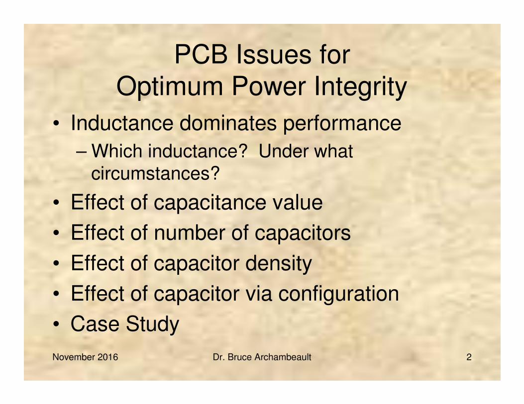
November 2016 Dr. Bruce Archambeault 6
Model for Plane Recharge Investigations
Port2 Port2
(4,5)(4,5)Port1Port1
(8,7)(8,7)
a = 12a = 12
b = 10b = 10
d = 35 mild = 35 milCdec Cdec
(4.05,5)(4.05,5)
Decoupling Capacitor :
C = 1uF
ESR = 30mOhm
ESL = 0.5nH
5.4=rε
DC voltage used to DC voltage used to
charge the power charge the power
plane plane
VdcVdc
I inputI input
Port3 Port3
(4,4.95)(4,4.95)
Port 2 represents IC current draw
November 2016 Dr. Bruce Archambeault 7
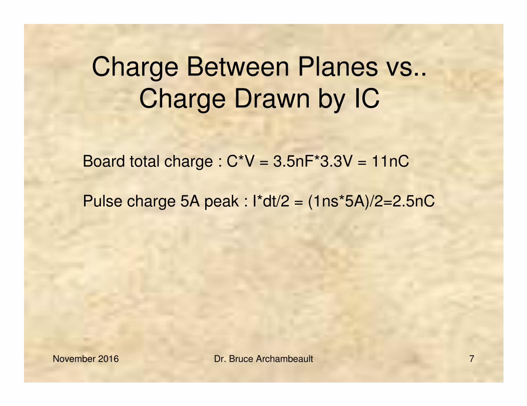
Charge Between Planes vs..
Charge Drawn by IC
Board total charge : C*V = 3.5nF*3.3V = 11nC
Pulse charge 5A peak : I*dt/2 = (1ns*5A)/2=2.5nC
November 2016 Dr. Bruce Archambeault 8
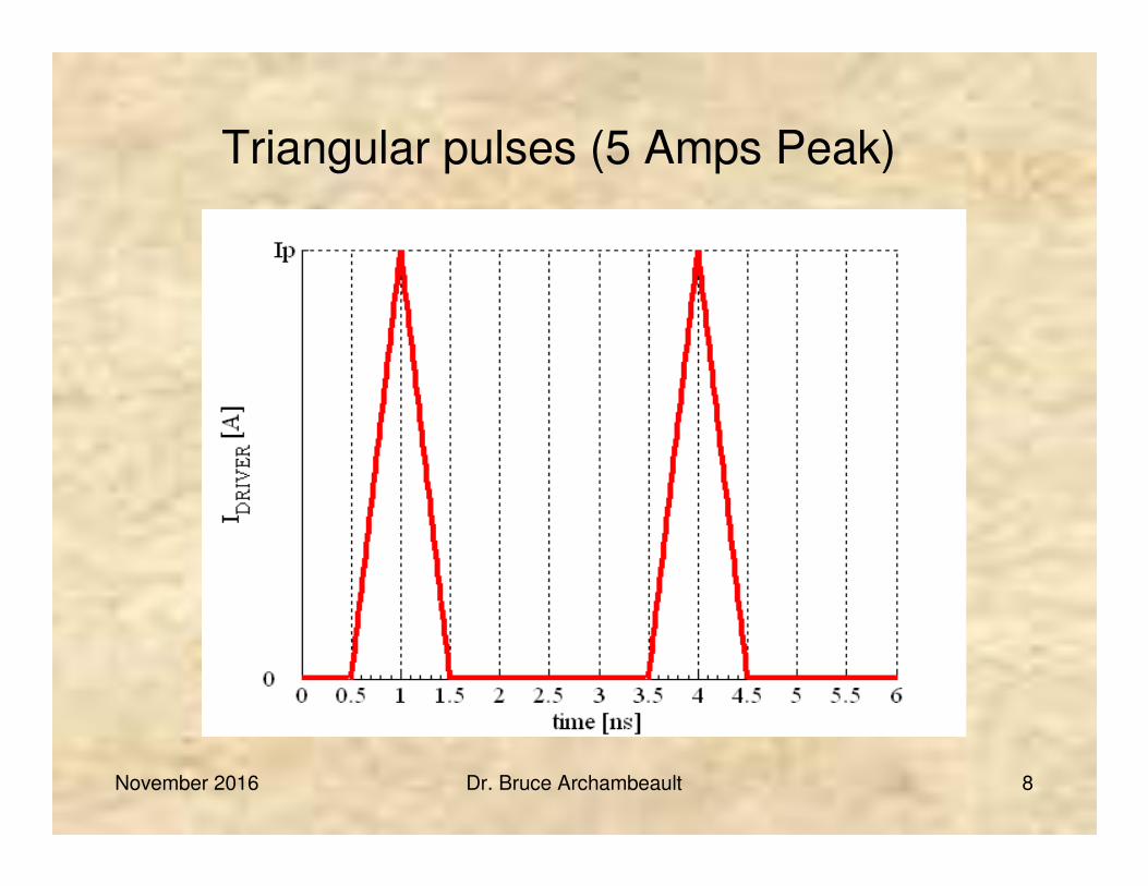
Triangular pulses (5 Amps Peak)
November 2016 Dr. Bruce Archambeault 9
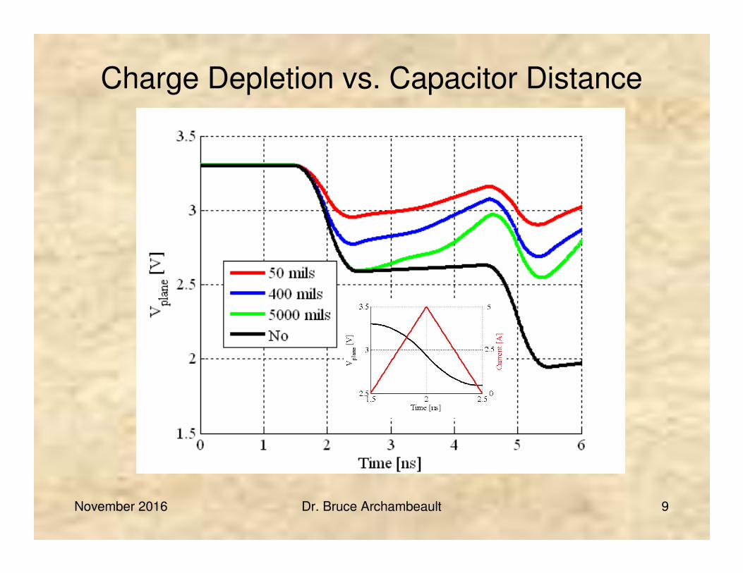
Charge Depletion vs. Capacitor Distance
November 2016 Dr. Bruce Archambeault 10
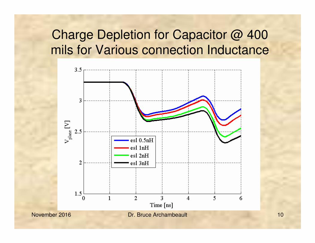
Charge Depletion for Capacitor @ 400 mils for Various connection Inductance

November 2016 Dr. Bruce Archambeault 11
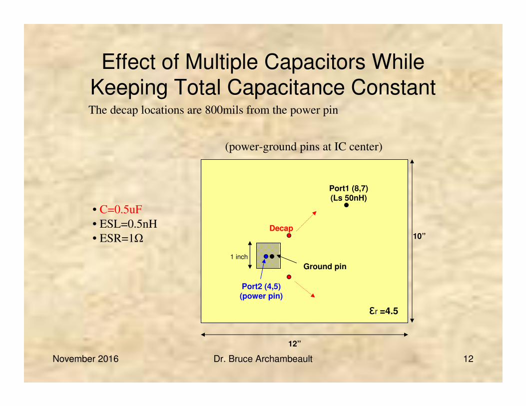
Effect of Multiple Capacitors While Keeping Total Capacitance Constant
(power-ground pins at IC center)
12”
10”
Port1 (8,7)(Ls 50nH)
Port2 (4,5)(power pin)
εr =4.5
Decap
Ground pin
1 inch
The decap locations are 800mils from the power pin
• C=1uF
• ESL=0.5nH
• ESR=1Ω
November 2016 Dr. Bruce Archambeault 12
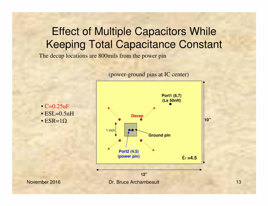
Effect of Multiple Capacitors While Keeping Total Capacitance Constant
(power-ground pins at IC center)
12”
10”
Port1 (8,7)(Ls 50nH)
Port2 (4,5)(power pin)
εr =4.5
Decap
Ground pin
1 inch
The decap locations are 800mils from the power pin
• C=0.5uF
• ESL=0.5nH
• ESR=1Ω
November 2016 Dr. Bruce Archambeault 13
Effect of Multiple Capacitors While Keeping Total Capacitance Constant
(power-ground pins at IC center)
12”
10”
Port1 (8,7)(Ls 50nH)
Port2 (4,5)(power pin) εr =4.5
Decap
Ground pin
1 inch
The decap locations are 800mils from the power pin
• C=0.25uF
• ESL=0.5nH
• ESR=1Ω

November 2016 Dr. Bruce Archambeault 14
Constant Capacitance
800 mil Distance
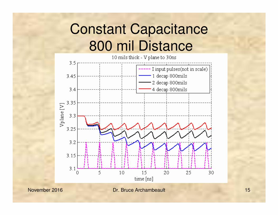
November 2016 Dr. Bruce Archambeault 15
Constant Capacitance
800 mil Distance
November 2016 Dr. Bruce Archambeault 16
Effect of Capacitor Value??
• Need enough charge to supply need
• Depends on connection inductance
November 2016 Dr. Bruce Archambeault 17
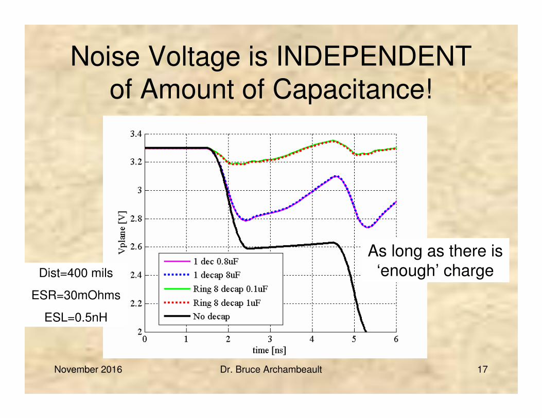
Noise Voltage is INDEPENDENT
of Amount of Capacitance!
As long as there is ‘enough’ chargeDist=400 mils
ESR=30mOhms
ESL=0.5nH

November 2016 Dr. Bruce Archambeault 18
What Happens if a 2nd Decoupling
Capacitor is placed near the First
Capacitor?
Observation
Point
Via #1Via #2 Moved in arc
around Observation
point while
maintaining 500 mil
distance to
observation point
500
mils
distance
November 2016 Dr. Bruce Archambeault 19
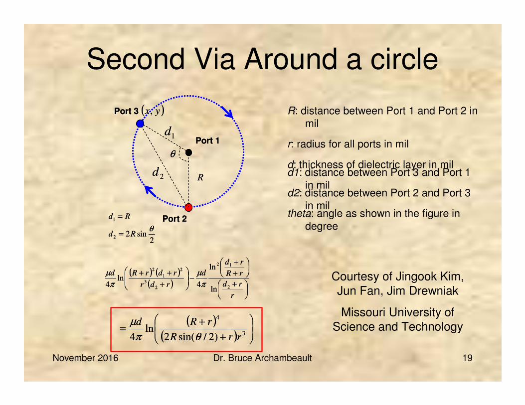
Second Via Around a circle
Port 2
Port 1
θ
( )yx,Port 3
( ) ( )( )
+
+
+
−
+
++
r
rd
rR
rd
d
rdr
rdrRd
2
12
2
3
2
1
2
ln
ln
4ln
4 π
µ
π
µ
2sin22
1
θRd
Rd
=
=
( )( )
+
+=
3
4
)2/sin(2ln
4 rrR
rRd
θπ
µ
1d
2dR
Port 2
Port 1
θ
( )yx,Port 3
( ) ( )( )
+
+
+
−
+
++
r
rd
rR
rd
d
rdr
rdrRd
2
12
2
3
2
1
2
ln
ln
4ln
4 π
µ
π
µ
2sin22
1
θRd
Rd
=
=
( )( )
+
+=
3
4
)2/sin(2ln
4 rrR
rRd
θπ
µ
1d
2dR
theta: angle as shown in the figure in
degree
d2: distance between Port 2 and Port 3
in mil
d1: distance between Port 3 and Port 1
in mil
d: thickness of dielectric layer in mil
r: radius for all ports in mil
R: distance between Port 1 and Port 2 in
mil
Courtesy of Jingook Kim,
Jun Fan, Jim Drewniak
Missouri University of
Science and Technology

November 2016 Dr. Bruce Archambeault 20
Effective Inductance for Various Distances to Decoupling CapacitorWith Second Capacitor (Via) Equal Distance Around Circle
Plane Seperation = 35 mil -- Via Diameter = 20 mil
500
600
700
800
900
1000
1100
1200
1300
1400
1500
1600
1700
1800
1900
2000
2100
0 50 100 150 200
Angle (degrees)
Ind
uctn
ace (
pH
)
250 mil
500mil
750 mil
1000 mil
November 2016 Dr. Bruce Archambeault 21
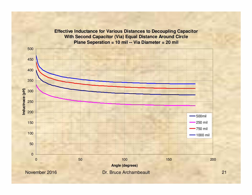
Effective Inductance for Various Distances to Decoupling CapacitorWith Second Capacitor (Via) Equal Distance Around Circle
Plane Seperation = 10 mil -- Via Diameter = 20 mil
0
50
100
150
200
250
300
350
400
450
500
0 50 100 150 200
Angle (degrees)
Ind
uc
tnac
e (
pH
)
500mil
250 mil
750 mil
1000 mil

November 2016 Dr. Bruce Archambeault 22
Second Via Along Side
Port 2
Port 1
( )yx,
R
Port 3
1d
2d
2
2
2
1 dRd +=
Port 2
Port 1
( )yx,
R
Port 3
1d
2d
2
2
2
1 dRd +=
d2: distance between Port 2 and Port 3 in mil
d1: distance between Port 3 and Port 1 in mil
d: thickness of dielectric layer in mil
r: radius for all ports in mil
R: distance between Port 1 and Port 2 in mil

November 2016 Dr. Bruce Archambeault 23
Effective Inductance for Various Distances to Decoupling CapacitorWith Second Capacitor (Via) Positioned Adjacent to First Capacitor
Plane Seperation = 35 mil -- Via Diameter = 20 mil
500
600
700
800
900
1000
1100
1200
1300
1400
1500
1600
1700
1800
1900
2000
2100
0 100 200 300 400 500 600 700 800 900 1000
Distance Between Capacitors (mils)
Ind
uctn
ace (
pH
)
500mil
250 mil
750 mil
1000 mil
November 2016 Dr. Bruce Archambeault 24
Understanding Inductance Effects and Proximity
1 via
10mm
2 via with degree 30°°°°
2 via with degree 90°°°° 2 via with degree 180°°°°
20cm
20cm
10cm
10cm

November 2016 Dr. Bruce Archambeault 25
Current Density
A/m2
[m]
[m]
A/m2
[m]
[m]
A/m2
[m]
[m]
A/m2
[m]
[m]
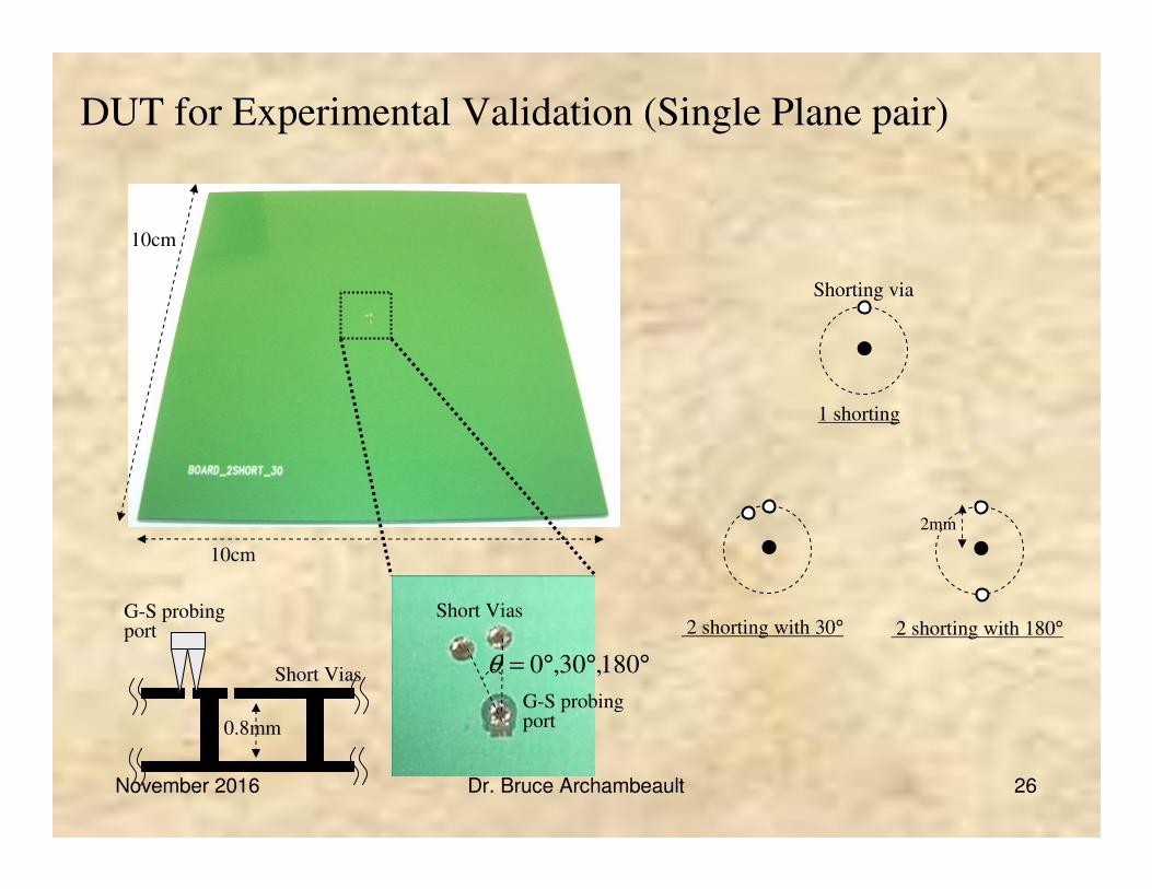
November 2016 Dr. Bruce Archambeault 26
2mm
2 shorting with 30° 2 shorting with 180°
10cm
10cm
G-S probingport
Short Vias
°°°= 180,30,0θ
0.8mm
G-S probingport
Short Vias
Shorting via
1 shorting
DUT for Experimental Validation (Single Plane pair)

November 2016 Dr. Bruce Archambeault 27
100
0.1
1
10
50 400
Frequency [MHz]
Imp
edan
ce [Ω
]
Measured Input Impedance
Experimental Validation (Single Plane Pair)
• Even in the case with two
shorting vias at opposite sides
(θ =180°), the inductance
value is 68.8% of that with
one shorting via
• As two shorting vias get
closer together, mutual
inductance between two
shorting vias increases.
0 50 100 150 200 250 300 350500
550
600
650
700
750
800
850
900
1000
theta (degree)
To
tal
ind
uct
ance
[p
H]
with only 1 via (852pH)
with 2 via with 180°
(586H = 68.8% × 852pH)
with 2 vias with 30° (687pH)
Equation
( )( )
+
+3
4
)2/sin(2ln
4 rrR
rRd
θπ
µ

November 2016 Dr. Bruce Archambeault 28
Multiple Capacitors
Decaps
GND
PWR
GND
PWR
Decaps
GND
PWR
GND
PWR
PWR_capGND_cap
GND
PWR
GND
PWR
Cavity1
Cavity2
Cavity3
Cavity4
PWR_capGND_cap
GND
PWR
GND
PWR
Cavity1
Cavity2
Cavity3
Cavity4
November 2016 Dr. Bruce Archambeault 29
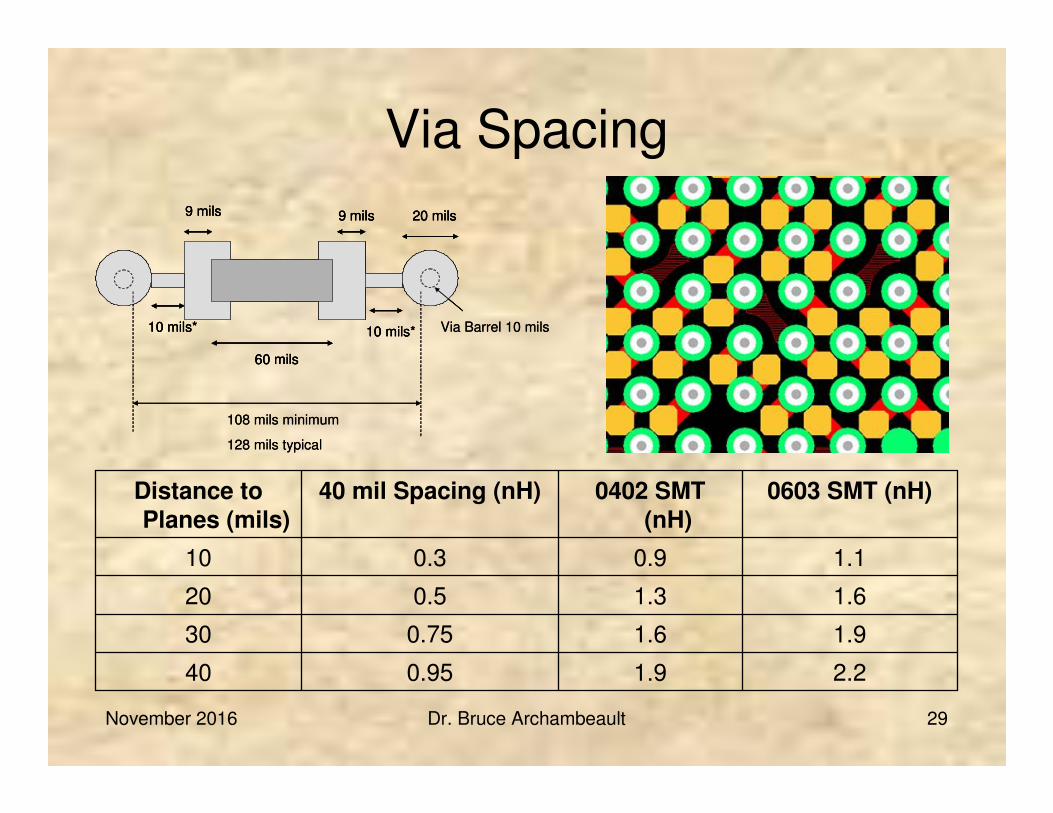
Via Spacing
Via Barrel 10 mils
60 mils
20 mils
10 mils*
9 mils9 mils
10 mils*
108 mils minimum
128 mils typical
Via Barrel 10 mils
60 mils
20 mils
10 mils*
9 mils9 mils
10 mils*
60 mils
20 mils
10 mils*
9 mils9 mils
10 mils*
108 mils minimum
128 mils typical
2.21.90.9540
1.91.60.7530
1.61.30.520
1.10.90.310
0603 SMT (nH)0402 SMT
(nH)
40 mil Spacing (nH)Distance to
Planes (mils)

November 2016 Dr. Bruce Archambeault 30Dr. Bruce Archambeault 30
0603 Size Cap Typical Mounting
Via Barrel 10 mils
60 mils
20 mils
10 mils*
9 mils9 mils
10 mils*
108 mils minimum
128 mils typical*Note: Minimum
distance is 10 mils but
more typical distance is
20 mils

November 2016 Dr. Bruce Archambeault 31Dr. Bruce Archambeault 31
Distance into board
to planes (mils)
0805 typical/minimum
(148 mils
between via
barrels)
0603
typical/minimum
(128 mils
between via
barrels)
0402 typical/minimum
(106 mils
between via
barrels)
10 1.2 nH 1.1 nH 0.9 nH
20 1.8 nH 1.6 nH 1.3 nH
30 2.2 nH 1.9 nH 1.6 nH
40 2.5 nH 2.2 nH 1.9 nH
50 2.8 nH 2.5 nH 2.1 nH
60 3.1 nH 2.7 nH 2.3 nH
70 3.4 nH 3.0 nH 2.6 nH
80 3.6 nH 3.2 nH 2.8 nH
90 3.9 nH 3.5 nH 3.0 nH
100 4.2 nH 3.7 nH 3.2 nH
Connection Inductance for Typical Capacitor Configurations
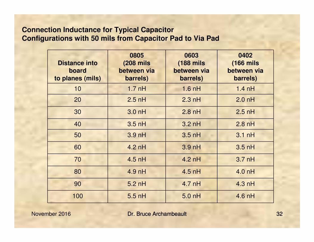
November 2016 Dr. Bruce Archambeault 32Dr. Bruce Archambeault 32
Connection Inductance for Typical Capacitor
Configurations with 50 mils from Capacitor Pad to Via Pad
Distance into board
to planes (mils)
0805
(208 mils
between via
barrels)
0603
(188 mils
between via
barrels)
0402
(166 mils
between via
barrels)
10 1.7 nH 1.6 nH 1.4 nH
20 2.5 nH 2.3 nH 2.0 nH
30 3.0 nH 2.8 nH 2.5 nH
40 3.5 nH 3.2 nH 2.8 nH
50 3.9 nH 3.5 nH 3.1 nH
60 4.2 nH 3.9 nH 3.5 nH
70 4.5 nH 4.2 nH 3.7 nH
80 4.9 nH 4.5 nH 4.0 nH
90 5.2 nH 4.7 nH 4.3 nH
100 5.5 nH 5.0 nH 4.6 nH
November 2016 Dr. Bruce Archambeault 33
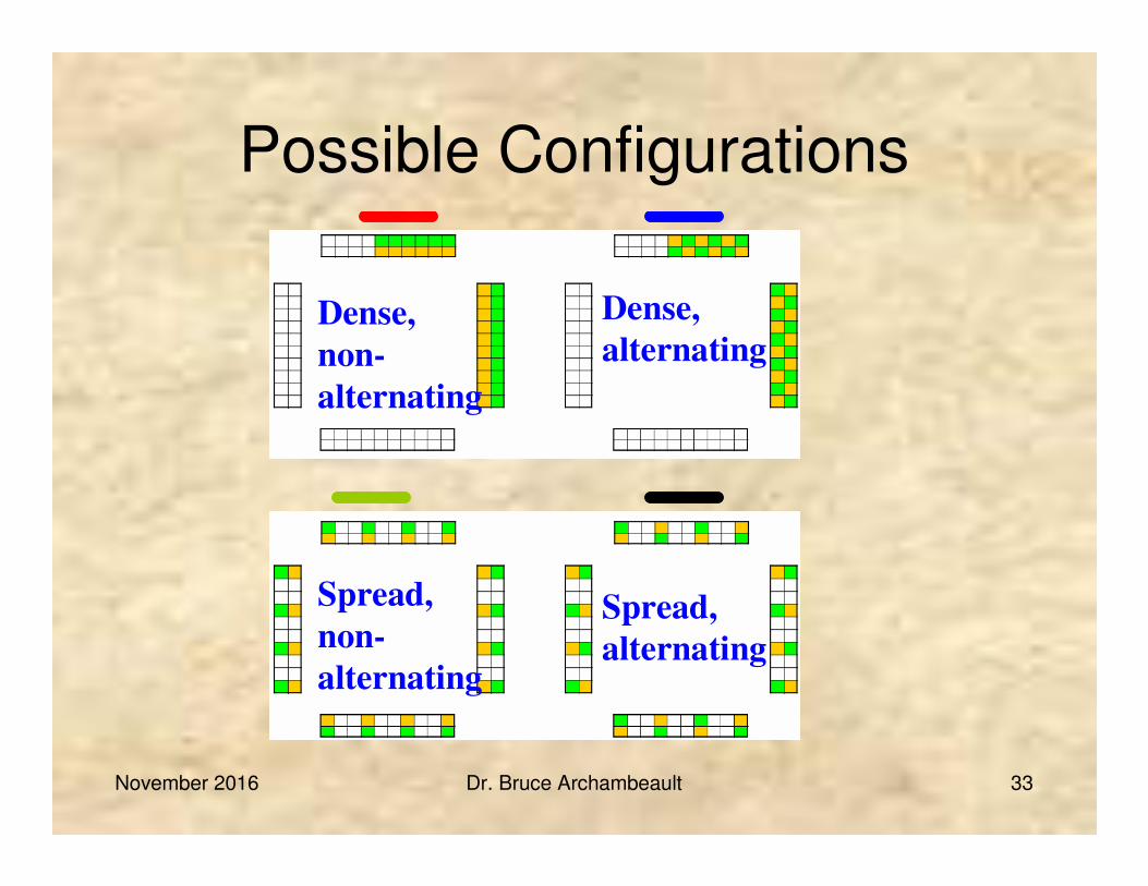
Possible Configurations
Dense,
non-
alternating
Dense,
alternating
Spread,
non-
alternating
Spread,
alternating
Dense,
non-
alternating
Dense,
alternating
Spread,
non-
alternating
Spread,
alternating

November 2016 Dr. Bruce Archambeault 34
Effective Inductance for 16 Decoupling Capacitors for Dense and Spread
Configurations and Plane Pair Depth
0
20
40
60
80
100
120
0 5 10 15 20 25 30 35 40
Distance into PCB (mils)
Eff
ecti
ve I
nd
ucta
nce (
pH
)
Dense Non-Alternating
Dense Alternating
Spread Non-AlternatingSpread Alternating
40 mil via spacing
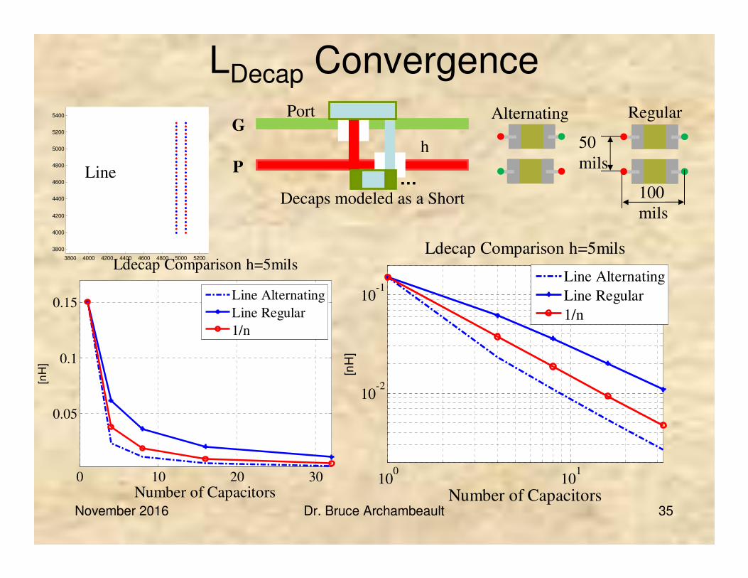
November 2016 Dr. Bruce Archambeault 35
LDecap Convergence
50
mils
Regular
100
mils
AlternatingG
P
h
…Decaps modeled as a Short
Port
3800 4000 4200 4400 4600 4800 5000 5200
3800
4000
4200
4400
4600
4800
5000
5200
5400
Line
100
101
10-2
10-1
Number of Capacitors
[nH
]
Ldecap Comparison h=5mils
Line Alternating
Line Regular
1/n
0 10 20 30
0.05
0.1
0.15
Number of Capacitors
[nH
]
Ldecap Comparison h=5mils
Line Alternating
Line Regular
1/n
November 2016 Dr. Bruce Archambeault 36
LDecap comparison (h=10mils, 0201)
AlternatingRegular Doublet
101
10-3
10-2
10-1
100
# of Decaps
L [
nH
]
LDecap vs # of Decaps, 0201
Regular
Alternating
Doublet
1/n
10 20 30 40 50 600
0.05
0.1
0.15
0.2
# of Decaps
L [
nH
]
LDecap vs # of Decaps, 0201
Regular
Alternating
Doublet
1/n
10mil
Short
GND
GNDPort
…
November 2016 Dr. Bruce Archambeault 37
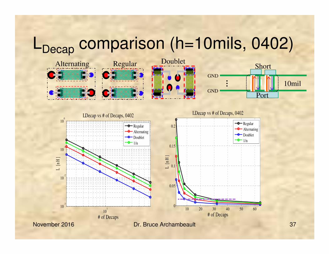
LDecap comparison (h=10mils, 0402)Alternating Regular Doublet
101
10-3
10-2
10-1
100
# of Decaps
L [
nH
]
LDecap vs # of Decaps, 0402
Regular
Alternating
Doublet
1/n
10 20 30 40 50 600
0.05
0.1
0.15
0.2
# of Decaps
L [
nH
]
LDecap vs # of Decaps, 0402
Regular
Alternating
Doublet
1/n
10mil
Short
GND
GNDPort
…

November 2016 Dr. Bruce Archambeault 38
LDecap comparison (h=10mils, 0603)Alternating Regular Doublet
101
10-3
10-2
10-1
100
# of Decaps
L [
nH
]
LDecap vs # of Decaps, 0603
Regular
Alternating
Doublet
1/n
10 20 30 40 50 600
0.05
0.1
0.15
0.2
# of Decaps
L [
nH
]
LDecap vs # of Decaps, 0603
Regular
Alternating
Doublet
1/n
10mil
Short
GND
GNDPort
…

November 2016 Dr. Bruce Archambeault 39
LDecap comparison (h=10mils, 0805)
Alternating Regular Doublet
101
10-3
10-2
10-1
100
# of Decaps
L [
nH
]
LDecap vs # of Decaps, 0805
Regular
Alternating
Doublet
1/n
10 20 30 40 50 600
0.05
0.1
0.15
0.2
# of Decaps
L [
nH
]
LDecap vs # of Decaps, 0805
Regular
Alternating
Doublet
1/n
10mil
Short
GND
GNDPort
…

November 2016 Dr. Bruce Archambeault 40
Observations
• Added via (capacitor) does not lower effective inductance to 70-75% of original single via case
• Thicker dielectric results in higher inductance
• Alternating PWR/GND can significantly reduce overall inductance

November 2016 Dr. Bruce Archambeault 41
Effect of Plane width on Inductance
Case1 : 10 inches
Case2 : 5 inches
Case3 : 2 inches1 inch
Port1 Port2

November 2016 Dr. Bruce Archambeault 42
Geometry Solid Plane
‘Capacitor’ Port‘IC’ Port (shorting via)
10 inches
12 inches
width
Solid Plane
‘Capacitor’ Port‘IC’ Port (shorting via)
10 inches
12 inches
width
‘IC’ Port (shorting via)
‘Capacitor’ Port
10 mils
‘IC’ Port (shorting via)
‘Capacitor’ Port
10 mils
Top View
Side View

November 2016 Dr. Bruce Archambeault 43
Inductance as a Function of
Plane Width
25741
13522
7095
54510
Inductance
(pH)
Plane Width
(inches)
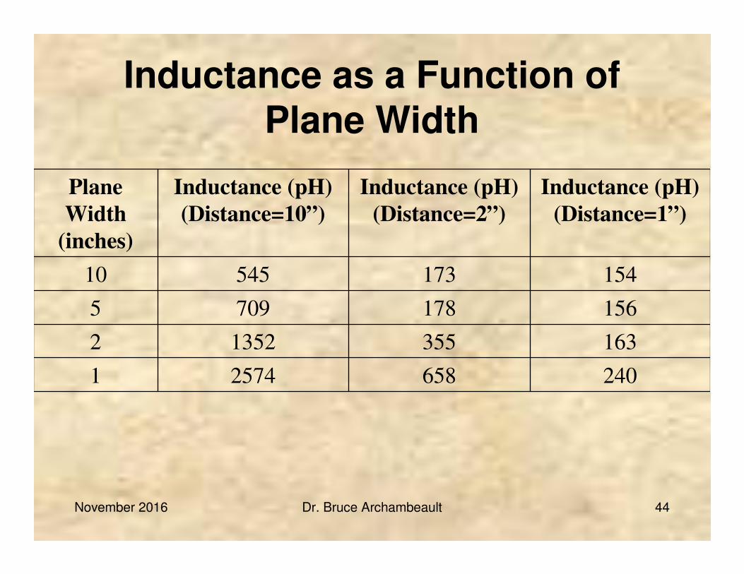
November 2016 Dr. Bruce Archambeault 44
Inductance as a Function of
Plane Width
24065825741
16335513522
1561787095
15417354510
Inductance (pH)
(Distance=1”)
Inductance (pH)
(Distance=2”)
Inductance (pH)
(Distance=10”)
Plane
Width
(inches)
November 2016 Dr. Bruce Archambeault 45
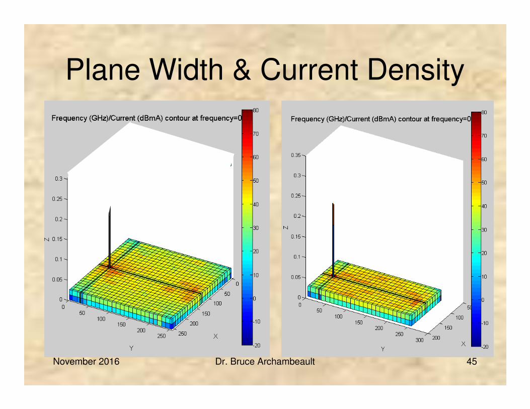
Plane Width & Current Density

November 2016 Dr. Bruce Archambeault 46
Typical PCB Power Design
November 2016 Dr. Bruce Archambeault 47Dr. Bruce Archambeault
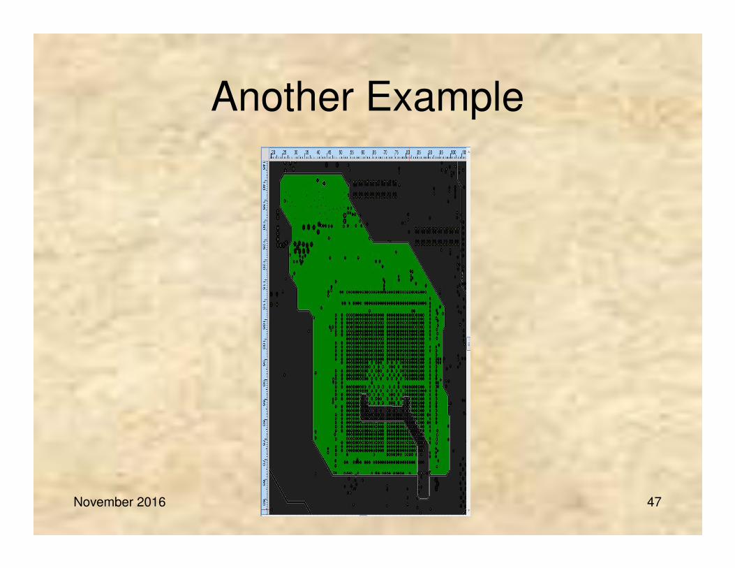
Another Example

November 2016 Dr. Bruce Archambeault 48
Sharp Angles Cause Current
‘Bunching’
(Increased Inductance)

November 2016 Dr. Bruce Archambeault 49
Geometry for Case Studies – Via Map
IC
region
~300 mils
16 Capacitors are
placed, to maintain
the symmetry
12”
12”
100 mils
1.2 mil
1oz Cu
1.2 mil
1oz Cu
1.2 mil
1oz Cu
0.6 mil
0.5oz
0.6 mil
0.5oz Cu
Copper
thicknessDielectric
thickness
44 Layer3 mil
3 mil
3 mil
3.5 mil
3.5 mil
Signal Net Location
Reference Net
Possible Power net
Location
16 Decap
16 Decap
16 Decap
16 Decap
16 Decap
16 Decap
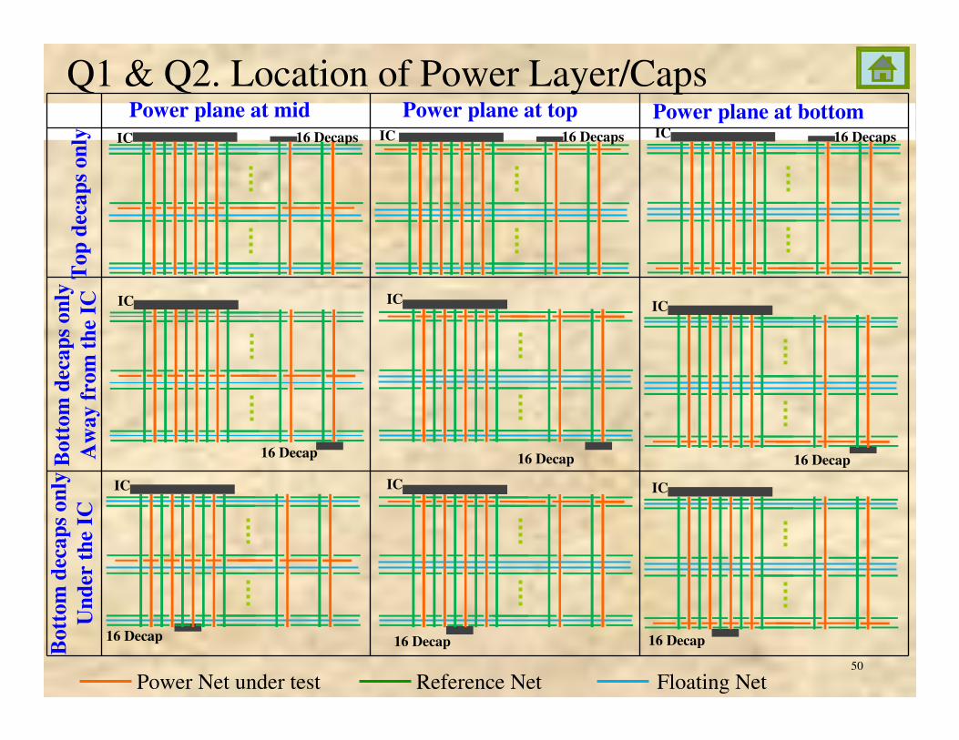
Power plane at mid
Top
dec
ap
son
lyB
ott
om
dec
ap
son
ly
Un
der
th
e IC
Power plane at top Power plane at bottom
Q1 & Q2. Location of Power Layer/CapsB
ott
om
dec
ap
son
ly
Aw
ay f
rom
th
e IC
IC 16 Decaps
IC
IC
IC 16 Decaps
IC
IC
IC 16 Decaps
IC
IC
Power Net under test Reference Net Floating Net50
November 2016 Dr. Bruce Archambeault 51
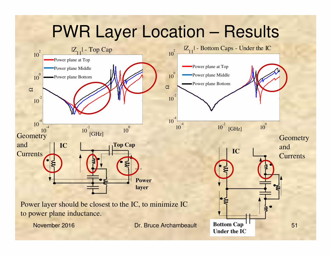
PWR Layer Location – Results
Bottom Cap
Under the IC
ICTop Cap
Power
layer
IC
…
10-4
10-2
100
10-4
10-2
100
102
[GHz]
Ω
|Z11
| - Top Cap
Top
Mid
Bottom
10-4
10-2
100
10-4
10-2
100
102
[GHz]
Ω
|Z11
| - Bottom Caps - Under the IC
Top
Mid
Bottom
Power layer should be closest to the IC, to minimize IC
to power plane inductance.
Geometry
and
Currents
Geometry
and
Currents
Power plane at Top
Power plane Middle
Power plane Bottom
Power plane at Top
Power plane Middle
Power plane Bottom
November 2016 Dr. Bruce Archambeault 52
10-4
10-2
100
10-4
10-2
100
102
[GHz]
Ω
|Z11
|- Top Pwr
Top Cap
Bottom Cap-Away
Bottom Cap- Under the IC
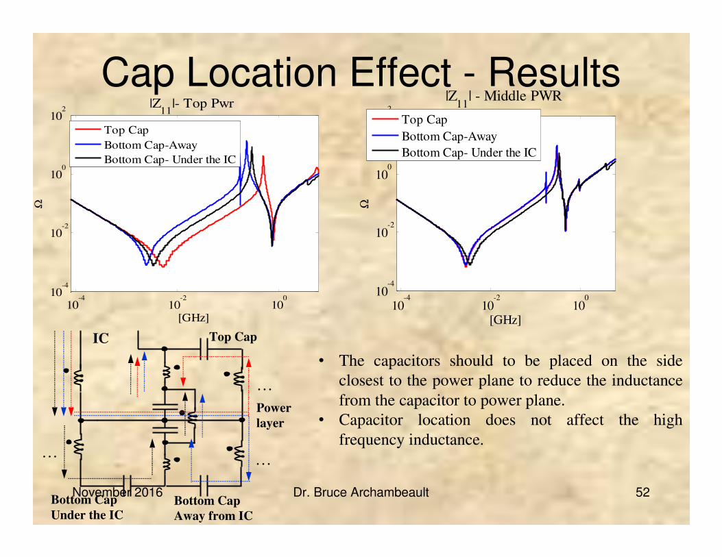
Cap Location Effect - Results
Top Cap
Bottom Cap
Away from IC
Bottom Cap
Under the IC
Power
layer
10-4
10-2
100
10-4
10-2
100
102
[GHz]
Ω
|Z11
| - Middle PWR
Top Cap
Bottom Cap-Away
Bottom Cap- Under the IC
IC
……
…
• The capacitors should to be placed on the side
closest to the power plane to reduce the inductance
from the capacitor to power plane.
• Capacitor location does not affect the high
frequency inductance.

November 2016 Dr. Bruce Archambeault 53
Q3. Effect of Ground Planes – Geometries
All ground planes With top nearby ground plane
With bottom nearby ground plane Only topmost and bottommost ground planes
IC IC
IC IC
Intermediate GND
planes removed
Intermediate GND
planes removed
Intermediate
GND planes
removed
Intermediate
GND planes
removed
Intermediate
GND planes
removed

November 2016 Dr. Bruce Archambeault 54
Effect of Ground Planes – Results
Top Cap
Power
layer
IC
…
10-4
10-2
100
10-4
10-2
100
102
[GHz]
Ω
|Z11
| - Top Cap
All GND Planes
Top Closest
Bottom Closest
Only Topmost & Bottommost
The closest ground plane from the power plane, is most important. Other Ground planes in the
stack up will not affect the Llow or Lhigh significantly.
Geometry and current path for no
GND plane case
Geometry
Geometry and current path for all
GND planes case
November 2016 Dr. Bruce Archambeault 55
Power Integrity Analysis Summary
• Physical cause of inductance (current path) identified for each portion of overall path
• Value of capacitance not as important as number of capacitors
• Via connection configuration can dramatically influence inductance
• If power/Ground-reference planes deep in PCB stackup, capacitor placement has less impact than might be expected
November 2016 Dr. Bruce Archambeault 56
Design Conclusions
• PWR/GND plane pair close to IC minimizes LIC
• Capacitors close to the power layer minimize the
inductance Ldecap from the capacitor to the power plane.
• PWR/GND plane separation small
• Placing Caps under the IC can benefit the design, if board is thin, or the plane inductance is large.
• Ground plane closest to the power layer affects the
response most, all other ground layer have very little influence.