Embed Size (px)
Citation preview

Application NoteSLVA617A–November 2014–Revised May 2015
bq76PL455A-Q1 Software Design Reference
StephenHolland
ABSTRACTThis application report contains examples of communication packets and sequences, which can be sent tothe bq76PL455A-Q1 device. The examples are meant to provide a programmer of a host systemcommunicating with a set of bq76PL455A-Q1 boards connected in series with a more complete picture ofthe communications process, as outlined in the bq76PL455A-Q1 16-Cell Battery Monitor with Passive CellBalancing data sheet, SLUSC51.
The bq76PL455A-Q1 data sheet should be used with this document.
All bq76PL455A-Q1 communications are represented in this document as a series of byte values. Dataare represented in hexadecimal format unless otherwise noted. Actual communication to and from thebq76PL455A-Q1 device is in standard 8 data bit, 1 stop bit, no-parity universal asynchronous receiver andtransmitter (UART) format. Each byte of data in a data packet is represented as a two characterhexadecimal number. For instance, a data value of 43 (decimal) is represented as 2B (hexadecimal). Thisdocument uses the following conventions:
• Data bytes sent from the host to a bq76PL455A-Q1 device are shown as a series of hexadecimalnumbers in red. (Other hexadecimal examples that are not sent to the host are otherwise indicatedwith text following.) Example:
89 01 00 0A 00 DA 83 This message reads the bq76PL455A-Q1 Device Address register.
• Data bytes sent from a bq76PL455A-Q1 device back to the host are shown as a series of hexadecimalnumbers in blue with (response) after the numbers.
00 01 C1 C0 (response) This response to the prior example message means, Device Address = 1.
The CRC in the message is a standard CRC-16 IBM, but with the most significant bit (MSB) and leastsignificant bit (LSB) stored in reverse order. Specifically in the previous sample message, a standardcalculation would yield a CRC-16 of 83DA, but it is stored in the message as DA83. Standard calculatorsare available online for verification of cyclic redundancy checks (CRCs). An example of this calculator isavailable at: www.lammertbies.nl/comm/info/crc-calculation.html.
Contents1 Auto-Addressing Sequence ................................................................................................ 22 Configuring Analog Front End (Thresholds and Channel Selections) ................................................ 73 Reading Voltages from Daisy-Chain Networked Boards.............................................................. 114 Reading Cell Voltages from a Single Board in Daisy-Chain Network ............................................... 155 Configuring and Using GPIO Pins ....................................................................................... 186 Saving Register Configuration to EEPROM ............................................................................ 237 Group Broadcast Write With Response ................................................................................. 278 General Broadcast Write With Response ............................................................................... 31
1SLVA617A–November 2014–Revised May 2015 bq76PL455A-Q1 Software Design ReferenceSubmit Documentation Feedback
Copyright © 2014–2015, Texas Instruments Incorporated
Auto-Addressing Sequence www.ti.com
1 Auto-Addressing SequenceEach bq76PL455A-Q1 device connected in a serial daisy-chain must have a unique device identifier(address) to be properly addressed by the host. There are two methods to set the address of thebq76PL455A-Q1 device. One method reads the general-purpose input/output (GPIO) pins and interpretsthe data as the address, while the other ignores the GPIO pins for the purpose of setting the address. Thissecond method allows the host to set the addresses of the bq76PL455A-Q1 device using a series ofcommands. These commands make use of flags in both the Device Configuration and Device Controlregisters.
The following procedure shows a sequence of commands that performs auto-addressing. The proceduremakes no assumption about the initial state of the communication drivers for the differentialcommunications ports of the serially connected bq76PL455A-Q1 devices. Therefore, some commandsmust be repeated 16 times to ensure any potential devices are properly configured.
By default, messages sent to the bottom device in a stack of serially connected devices propagate“upstream” at all times. That is to say, the single-ended receiver, high-side differential transmitter, and low-side differential receiver on every device are always enabled and cannot be disabled. Communication inthe opposite direction, “downstream," can be either disabled or enabled using the CommunicationsConfiguration register, and all downstream communication is disabled by default. Specifically, the disabledcommunication channels are the low-side differential transmitter, the high-side differential receiver, and thesingle-ended transmitter. For full communication both upstream and downstream, enable the following:• All differential transmitters and receivers for devices from the second device in the chain to the next-to-
last device in the chain• The low-side differential transmitter on the last (top-most) device in the chain• The single-ended transmitter on the first device in the chain
Typically, when battery packs are first assembled and configured, the bq76PL455A-Q1 devices thatmanage the cells are preconfigured with device addresses, communication timeout, and power-downsettings. This configuration leaves them in a powered-down state shortly after the configuration controlleris disconnected. In this state, a single WAKE pulse signal to the bottom-most device in a chain of deviceswakes up all devices in the chain. Typically, all devices already have their addresses and communicationsparameters configured properly. If this is the case, auto-addressing is typically not necessary.
1.1 Summary of Steps for Auto-Addressing
1. Make sure all boards are awake and ready to receive the AUTO-ADDRESS ENABLE command.2. Turn on the downstream communications drivers on all devices in the chain.3. Place all devices into auto-address learn mode.4. Send out new addresses to all possible bq76PL455A-Q1 device addresses, in incremental order,
starting at 0.5. Read back the value stored in the Device Address register from each newly addressed device, starting
at address 0 and proceeding sequentially. The last bq76PL455A-Q1 device to successfully respond isthe last device in the serial chain.
6. Turn off the high-side communications receiver on the last (top-most) device in the chain.7. Turn off the single-ended transmitter on all except the lowest device in the chain.
1.2 Detailed Steps for Auto-Addressing
1.2.1 Fully Enable Differential Interfaces and Select Auto-Addressing ModeWrite to the Communication Configuration register (address 16 to 17) of each potential bq76PL455A-Q1device in the network. This message is a broadcast message, so all connected bq76PL455A-Q1 devicesare affected. The example messages use 8-bit register addressing. For the purpose of this example,assume all devices in the chain are in the powered-up state. A BROADCAST command is used to set auniform communications configuration on all devices. Specific configurations for the bottom-most and top-most device are made later in the configuration sequence.
2 bq76PL455A-Q1 Software Design Reference SLVA617A–November 2014–Revised May 2015Submit Documentation Feedback
Copyright © 2014–2015, Texas Instruments Incorporated
www.ti.com Auto-Addressing Sequence
In the example message, the following configuration is made:• Set the baud rate to 250K (for the single-ended interface) by setting the BAUD bits to 01.• Enable the single-ended transmitter by setting the UART_EN bit.• Enable the high-side differential receiver by setting the COMM_HIGH_EN bit.• Enable the low-side differential transmitter by setting the DIFF_COMM_EN bit.
NOTE: In this example, the differential FAULT interfaces remain disabled. Please refer to the datasheet description of the Communication Configuration register for details on how to enablethis interface.
F2 10 10E0 3F35 Configure communications as per the previous descriptionF2 = General Broadcast Write Without Response 2 bytes (8-bit register
addressing)10 = Register Address 16 (Communication Configuration register)10E0 = Data3F35 = CRC
1.2.2 Put Devices into Auto-Address Learning ModeSet the ADDR_SEL bit in the Device Configuration register (address 14) to allow for address selectionthrough the auto-address selection method. Then, set the AUTO_ADDRESS bit in the Device Controlregister (address 12). These messages are broadcast messages, so all connected bq76PL455A-Q1devices are affected. This example uses 8-bit register addressing. When writing to the DeviceConfiguration register, other configuration parameters (such as charge pump, internal regulator,comparator, and fault latching functions) are affected. For this example, no other default values arechanged. However, TI recommends consulting the data sheet for other possible configurations.
F1 0E 10 545F Configure the bq76PL455A-Q1 device to use auto-addressing to select addressF1 = General Broadcast Write Without Response 1 byte (8-bit register
addressing)0E = Register Address 14 (Device Configuration)10 = Data (set the ADDR_SEL bit)545F = CRC
F1 0C 08 5535 Configure the bq76PL455A-Q1 device to enter auto-address modeF1 = General Broadcast Write Without Response 1 byte (8-bit register
addressing)0C = Register Address 12 (Device Control)08 = Data (set the AUTO_ADDRESS bit)5535 = CRC
1.2.3 Set New Addresses for Daisy-Chained DevicesWrite a new address sequentially to the Device Address register (address 10) of each potentialbq76PL455A-Q1 device. This message is a broadcast message, so all connected bq76PL455A-Q1devices are affected. Eight-bit register addressing is used in the example. This addressing step is typicallyrepeated a sufficient number of times to set all device addresses in the expected stack of devices. In theprovided example, the addressing step is repeated 16 times, one time for each potential device address.This addressing step should be curtailed appropriately in the user’s application. The lowest addressshould be set to 0.
3SLVA617A–November 2014–Revised May 2015 bq76PL455A-Q1 Software Design ReferenceSubmit Documentation Feedback
Copyright © 2014–2015, Texas Instruments Incorporated
Auto-Addressing Sequence www.ti.com
NOTE: The full available range in the register is 0 to 31. However, as per the data sheet, themaximum value should be restricted to 16.
F1 0A 00 5753 Configure device 1 to address 0F1 = Broadcast Write Without Response 1 byte (8-bit register addressing)0A = Register Address 10 (Device Address register)00 = Data (address = 00)5753 = CRC
F1 0A 01 9693 Configure device 2 to address 1F1 0A 02 D692 Configure device 3 to address 2F1 0A 03 1752 Configure device 4 to address 3F1 0A 04 5690 Configure device 5 to address 4F1 0A 05 9750 Configure device 6 to address 5F1 0A 06 D751 Configure device 7 to address 6F1 0A 07 1691 Configure device 8 to address 7F1 0A 08 5695 Configure device 9 to address 8F1 0A 09 9755 Configure device 10 to address 9F1 0A 0A D754 Configure device 11 to address 10F1 0A 0B 1694 Configure device 12 to address 11F1 0A 0C 5756 Configure device 13 to address 12F1 0A 0D 9696 Configure device 14 to address 13F1 0A 0E D697 Configure device 15 to address 14F1 0A 0F 1757 Configure device 16 to address 15
1.2.4 Find bq76PL455A-Q1 at Top of StackTry to read the Device Address register (address 10) of the bq76PL455A-Q1 from all the boards in thenetwork. Start with the bq76PL455A-Q1 at Device Address 0 and increment to the highest expectedaddress (or the maximum address of 16), until the read command fails to illicit a response. The lastbq76PL455A-Q1 to respond is the bq76PL455A-Q1 at the top of stack (ToS). The example commands aresingle device messages (that is, not broadcast) and utilize 8-bit register addressing. In this example, thereare two boards in the chain of devices.
81 00 0A 00 2E9C Read Device Address register on device 1 (at address 0)81 = Single Device Write With Response (8-bit register addressing)00 = Device Address 00A = Register 10 (Device Address register)00 = Expected response data bytes: 12E9C = CRC
00 00 0000 (response)Response from device 2 (at address 1)00 = Response of 1 byte00 = Data (device address is 0)0000 = CRC
81 01 0A 00 7F5C Read Device Address register on device 2 (at address 1)81 = Single Device Write With Response (8-bit register addressing)01 = Device Address 10A = Register 10 (Device Address register)
4 bq76PL455A-Q1 Software Design Reference SLVA617A–November 2014–Revised May 2015Submit Documentation Feedback
Copyright © 2014–2015, Texas Instruments Incorporated

www.ti.com Auto-Addressing Sequence
00 = Expected response data bytes: 17F5C = CRC
00 01 C1C0 (response)Response from device 2 (at address 1)00 = Response of 1 byte01 = Data (device address is 1)C1C0 = CRC
81 02 0A 00 8F5C Read Device Address register on device 3 (at address 2)81 = Single Device Write With Response (8-bit register addressing)02 = Device Address 20A = Register 10 (Device Address register)00 = Expected response data bytes: 18F5C = CRC
(no response) Since there is no response, the previous board is at ToS.
1.2.5 Disable High-Side Receiver on Differential Interface on Top of StackTo reduce current consumption and turn off the receipt of undesired messages due to noise fromnonexistent boards above the top-most device, this message turns off the high-side differential receiverinterface on the bq76PL455A-Q1 device at the top of the stack (bq76PL455A-Q1 at Device Address 1 inthis example). Specifically, this message clears the COMM_HIGH_EN bit in the CommunicationConfiguration register (address 16 to 17) on the top-most device in the chain.
92 01 10 1020 B5FC Set the communication configuration on top-most device92 = Single Device Write Without Response 2 bytes (8-bit register
addressing)01 = Device Address 1 (top device in this example)10 = Register 161020 = Data for Communication Configuration register (0001 0000 0010 0000:
see data sheet)B5FC = CRCBits set in the Communication Configuration register are:
• BAUD = 01 (250K)
• DIFF_COMM_EN = 1
• (All other bits in register = 0)Baud is set to 250K, single-ended transmitter is disabled, high-side differentialreceiver is disabled, low-side differential transmitter is enabled, and all other bitsare left at default (disabled).
1.2.6 Disable Low-Side Transmitter on Differential Interface on Bottom of StackTo reduce current consumption and turn off the transmission of undesired messages over the differentialinterface to devices (which do not exist) below the bottom device, this message turns off the low-sidedifferential transmitter interface on the bq76PL455A-Q1 device at the bottom of stack (bq76PL455A-Q1 atDevice Address 0 in this example). Specifically, this message clears the DIFF_COMM_EN bit in theCommunication Configuration register (address 16 to 17) on the bottom-most device in the chain.
5SLVA617A–November 2014–Revised May 2015 bq76PL455A-Q1 Software Design ReferenceSubmit Documentation Feedback
Copyright © 2014–2015, Texas Instruments Incorporated
Auto-Addressing Sequence www.ti.com
92 00 10 10C0 B588 Set the communication configuration on top-most device92 = Single Device Write Without Response 2 bytes (8-bit register
addressing)00 = Device Address 0 (bottom device in this example)10 = Register 1610C0 = Data for Communication Configuration register (0001 0000 1100 0000:
see data sheet)B588 = CRCBits set in the Communication Configuration register are:
• BAUD = 01 (250K)
• UART_EN = 1
• COMM_HIGH_EN = 1
• (All other bits in register = 0)Baud is set to 250K, single-ended transmitter is enabled, high-side differentialreceiver is enabled, low-side differential transmitter is disabled, and all other bitsare left at default (disabled).
1.2.7 Clear All FaultsStarting at the top of stack of boards, clear all existing faults. Begin at the top of stack to prevent faultsfrom “higher” units from re-enabling faults as they propagate down the stack.
92 01 52 FFC0 5850 Clear all fault bits in the Fault Summary register on device 1 (top of stack)92 = Single Device Write Without Response 2 bytes (8-bit register
addressing)01 = Device Address 152 = Register 82 (Fault Summary register)FFC0 = Data (all defined bits set to 1 to clear the faults)5850 = CRC
92 00 52 FFC0 59AC Clear all fault bits in the Fault Summary register on device 1 (top of stack)92 = Single Device Write Without Response 2 bytes (8-bit register
addressing)00 = Device Address 052 = Register 82 (Fault Summary register)FFC0 = Data (all defined bits set to 1 to clear the faults)59AC = CRC
6 bq76PL455A-Q1 Software Design Reference SLVA617A–November 2014–Revised May 2015Submit Documentation Feedback
Copyright © 2014–2015, Texas Instruments Incorporated
www.ti.com Configuring Analog Front End (Thresholds and Channel Selections)
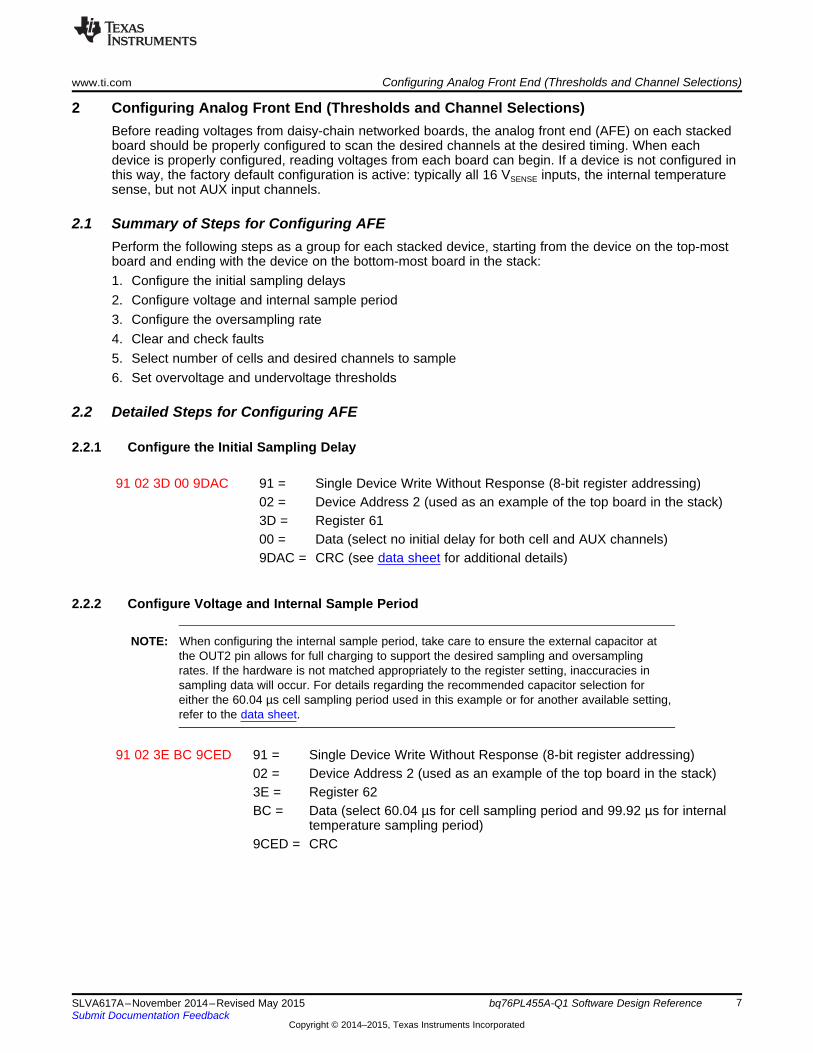
2 Configuring Analog Front End (Thresholds and Channel Selections)Before reading voltages from daisy-chain networked boards, the analog front end (AFE) on each stackedboard should be properly configured to scan the desired channels at the desired timing. When eachdevice is properly configured, reading voltages from each board can begin. If a device is not configured inthis way, the factory default configuration is active: typically all 16 VSENSE inputs, the internal temperaturesense, but not AUX input channels.
2.1 Summary of Steps for Configuring AFEPerform the following steps as a group for each stacked device, starting from the device on the top-mostboard and ending with the device on the bottom-most board in the stack:1. Configure the initial sampling delays2. Configure voltage and internal sample period3. Configure the oversampling rate4. Clear and check faults5. Select number of cells and desired channels to sample6. Set overvoltage and undervoltage thresholds
2.2 Detailed Steps for Configuring AFE
2.2.1 Configure the Initial Sampling Delay
91 02 3D 00 9DAC 91 = Single Device Write Without Response (8-bit register addressing)02 = Device Address 2 (used as an example of the top board in the stack)3D = Register 6100 = Data (select no initial delay for both cell and AUX channels)9DAC = CRC (see data sheet for additional details)
2.2.2 Configure Voltage and Internal Sample Period
NOTE: When configuring the internal sample period, take care to ensure the external capacitor atthe OUT2 pin allows for full charging to support the desired sampling and oversamplingrates. If the hardware is not matched appropriately to the register setting, inaccuracies insampling data will occur. For details regarding the recommended capacitor selection foreither the 60.04 µs cell sampling period used in this example or for another available setting,refer to the data sheet.
91 02 3E BC 9CED 91 = Single Device Write Without Response (8-bit register addressing)02 = Device Address 2 (used as an example of the top board in the stack)3E = Register 62BC = Data (select 60.04 µs for cell sampling period and 99.92 µs for internal
temperature sampling period)9CED = CRC
7SLVA617A–November 2014–Revised May 2015 bq76PL455A-Q1 Software Design ReferenceSubmit Documentation Feedback
Copyright © 2014–2015, Texas Instruments Incorporated
Configuring Analog Front End (Thresholds and Channel Selections) www.ti.com
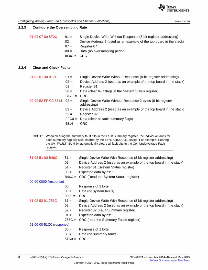
2.2.3 Configure the Oversampling Rate
91 02 07 00 8F0C 91 = Single Device Write Without Response (8-bit register addressing)02 = Device Address 2 (used as an example of the top board in the stack)07 = Register 0700 = Data (no oversampling period)8F0C = CRC
2.2.4 Clear and Check Faults
91 02 51 38 B17E 91 = Single Device Write Without Response (8-bit register addressing)02 = Device Address 2 (used as an example of the top board in the stack)51 = Register 8138 = Data (clear fault flags in the System Status register)B17E = CRC
92 02 52 FF C0 5814 92 = Single Device Write Without Response 2 bytes (8-bit registeraddressing)
02 = Device Address 2 (used as an example of the top board in the stack)52 = Register 82FFC0 = Data (clear all fault summary flags)5814 = CRC
NOTE: When clearing the summary fault bits in the Fault Summary register, the individual faults foreach summary flag are also cleared by the bq76PL455A-Q1 device. For example, clearingthe UV_FAULT_SUM bit automatically clears all fault bits in the Cell Undervoltage Faultregister.
81 02 51 00 B46C 81 = Single Device Write With Response (8-bit register addressing)02 = Device Address 2 (used as an example of the top board in the stack)51 = Register 81 (System Status register)00 = Expected data bytes: 1B46C = CRC (Read the System Status register)
00 00 0000 (response)00 = Response of 1 byte00 = Data (no system faults)0000 = CRC
81 02 52 01 755C 81 = Single Device Write With Response (8-bit register addressing)02 = Device Address 2 (used as an example of the top board in the stack)52 = Register 82 (Fault Summary register)01 = Expected data bytes: 1755C = CRC (read the Summary Faults register)
01 00 00 51C0 (response)00 = Response of 1 byte00 = Data (no summary faults)51C0 = CRC
8 bq76PL455A-Q1 Software Design Reference SLVA617A–November 2014–Revised May 2015Submit Documentation Feedback
Copyright © 2014–2015, Texas Instruments Incorporated
www.ti.com Configuring Analog Front End (Thresholds and Channel Selections)
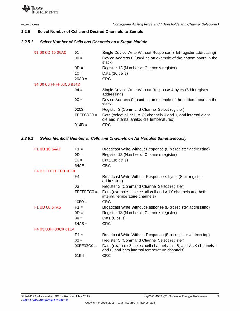
2.2.5 Select Number of Cells and Desired Channels to Sample
2.2.5.1 Select Number of Cells and Channels on a Single Module
91 00 0D 10 29A0 91 = Single Device Write Without Response (8-bit register addressing)00 = Device Address 0 (used as an example of the bottom board in the
stack)0D = Register 13 (Number of Channels register)10 = Data (16 cells)29A0 = CRC
94 00 03 FFFF03C0 914D94 = Single Device Write Without Response 4 bytes (8-bit register
addressing)00 = Device Address 0 (used as an example of the bottom board in the
stack)0003 = Register 3 (Command Channel Select register)FFFF03C0 = Data (select all cell, AUX channels 0 and 1, and internal digital
die and internal analog die temperatures)914D = CRC
2.2.5.2 Select Identical Number of Cells and Channels on All Modules Simultaneously
F1 0D 10 54AF F1 = Broadcast Write Without Response (8-bit register addressing)0D = Register 13 (Number of Channels register)10 = Data (16 cells)54AF = CRC
F4 03 FFFFFFC0 10F0F4 = Broadcast Write Without Response 4 bytes (8-bit register
addressing)03 = Register 3 (Command Channel Select register)FFFFFFC0 = Data (example 1: select all cell and AUX channels and both
internal temperature channels)10F0 = CRC
F1 0D 08 54A5 F1 = Broadcast Write Without Response (8-bit register addressing)0D = Register 13 (Number of Channels register)08 = Data (8 cells)54A5 = CRC
F4 03 00FF03C0 61E4F4 = Broadcast Write Without Response (8-bit register addressing)03 = Register 3 (Command Channel Select register)00FF03C0 = Data (example 2: select cell channels 1 to 8, and AUX channels 1
and 0, and both internal temperature channels)61E4 = CRC
9SLVA617A–November 2014–Revised May 2015 bq76PL455A-Q1 Software Design ReferenceSubmit Documentation Feedback
Copyright © 2014–2015, Texas Instruments Incorporated
Configuring Analog Front End (Thresholds and Channel Selections) www.ti.com
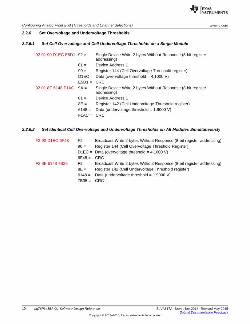
2.2.6 Set Overvoltage and Undervoltage Thresholds
2.2.6.1 Set Cell Overvoltage and Cell Undervoltage Thresholds on a Single Module
92 01 90 D1EC E5D1 92 = Single Device Write 2 bytes Without Response (8-bit registeraddressing)
01 = Device Address 190 = Register 144 (Cell Overvoltage Threshold register)D1EC = Data (overvoltage threshold = 4.1000 V)E5D1 = CRC
92 01 8E 6148 F1AC 9A = Single Device Write 2 bytes Without Response (8-bit registeraddressing)
01 = Device Address 18E = Register 142 (Cell Undervoltage Threshold register)6148 = Data (undervoltage threshold = 1.9000 V)F1AC = CRC
2.2.6.2 Set Identical Cell Overvoltage and Undervoltage Thresholds on All Modules Simultaneously
F2 90 D1EC 6F48 F2 = Broadcast Write 2 bytes Without Response (8-bit register addressing)90 = Register 144 (Cell Overvoltage Threshold Register)D1EC = Data (overvoltage threshold = 4.1000 V)6F48 = CRC
F2 8E 6148 7B35 F2 = Broadcast Write 2 bytes Without Response (8-bit register addressing)8E = Register 142 (Cell Undervoltage Threshold register)6148 = Data (undervoltage threshold = 1.9000 V)7B35 = CRC
10 bq76PL455A-Q1 Software Design Reference SLVA617A–November 2014–Revised May 2015Submit Documentation Feedback
Copyright © 2014–2015, Texas Instruments Incorporated
www.ti.com Reading Voltages from Daisy-Chain Networked Boards
3 Reading Voltages from Daisy-Chain Networked BoardsWhen bq76PL455A-Q1 devices are networked, with each device monitoring a section of a stack of cells,try to capture the voltages of each substack as synchronously as possible. This snapshot can be obtainedif all devices in the stack are sampling in parallel.
Different methods may be used to command stacked devices to initiate the sampling and request theresults, depending on the needs and limitations of the system.
One implementation method (Method 1) is to combine the sampling request, storage of results, andrequest for response from all boards into a single command. This method uses the fewest number ofbytes to accomplish the task, but requires the host to parse a potentially large response message, whichmay tax the abilities of a small, inexpensive microcontroller. This method is useful if all devices areconfigured to sample the same number of channels in the same manner with identical sampling periodsand oversamples.
Another implementation method (Method 2) is to broadcast a “sample and store” request, then read theresults individually from each device using several commands. This method has the disadvantage of usinggreater communication bandwidth, but has the advantage of reducing the size of individual responses andreducing the message parsing requirements. This method is useful if all devices are not configured tosample at identical sampling periods or oversamples.
Although these two methods are the most common, other methods may be implemented. Each methodcan be implemented using either 8-bit or 16-bit register addressing. A brief overview of the methodsfollows:1. Broadcast a SYNCHRONOUSLY SAMPLE CHANNELS request using a Broadcast Write With
Response command. All selected channels are sampled, the results stored, and each device respondswith the information starting with the device at the highest address and ending with the device at thelowest address.
2. Broadcast a SYNCHRONOUSLY SAMPLE CHANNELS request using a Broadcast Write WithoutResponse command. All selected channels are sampled, and the results are stored, but no responsesare generated. Follow this command with a broadcast READ SAMPLED VALUES command. Thestored data from all units are sent starting with the device at the highest address and ending with thedevice at the lowest address.
3. Broadcast a SYNCHRONOUSLY SAMPLE CHANNELS request using a Broadcast Write WithoutResponse command. All selected channels are sampled, and the results are stored, but no response isgenerated. Follow this command with a series of Single Device Write With Response commands toREAD SAMPLED VALUES. The stored data from the addressed unit are sent back to the host. Eachdevice in the stack should have its data read, ideally starting with the device at the highest addressand ending with the device at the lowest address, though order is not critical in this case.
Each method can be implemented with limitations to the number of responses by setting the HighestAddress to Respond field in the data byte or bytes of the command. Further message modification ispossible by sending the sampling parameters as part of the command message.
3.1 Summary of Steps for Reading Voltages from Daisy-Chain Networked BoardsMethod 1:Broadcast a trigger to sample, store, and return the results from all boards.
Method 2:1. Broadcast a trigger to all boards in the network to start sampling the selected cell, auxiliary channels,
temperature channels, and any of the ancillary channels.2. Query each board individually in sequence for the data collected during the last sampling snapshot.
11SLVA617A–November 2014–Revised May 2015 bq76PL455A-Q1 Software Design ReferenceSubmit Documentation Feedback
Copyright © 2014–2015, Texas Instruments Incorporated
Reading Voltages from Daisy-Chain Networked Boards www.ti.com
3.2 Method 1: Detailed Steps for Reading Voltages from Daisy-Chain Networked BoardsSend Broadcast Request to All bq76PL455A-Q1 Devices to Sample, Store, and Return ResultsThis message writes to the Command register (address 2). The command written is theSYNCHRONOUSLY SAMPLE CHANNELS command, which is contained in the upper 3 bits of thecommand data byte. The lower 5 bits of the command data byte contain the address of the highest devicein the chain (if all devices in the stack are being queried). This example assumes that three devices are inthe stack. Only a general overview of the response message is given in this subsection. For a detailedbreakdown of a potential response message, see Section 3.3.2 (concatenate the three responses shownthere).
E1 02 02 D097 E1 = Broadcast Write With Response, 8-bit register addressing, 1 data byte inmessage
02 = Register Address 2 (Command register)02 = 000 00010
000 = SYNCHRONOUSLY SAMPLE CHANNELS command00010 = Highest address to respond is device at address 2
D097 = CRC
Response (device 2), Response (device 1), Response (device 0)
The concatenated responses may come as a single burst of bytes, or they may be interspersed withdelays based on the sampling settings configured into the devices in the chain. In this example, theresponse is comprised of three complete messages, one from each responding device, although it mayappear to be one long, continuous message.
It is extremely important to understand the delays associated with this command. Particularly, theresponse from the first responding device (that is, the device at the highest address in the stack) will notrespond, until it has completed sampling. This means the host may not receive a reply for severalmilliseconds, depending on the sample period and oversampling settings configured into the bq76PL455A-Q1 device.
NOTE: If communication timeout periods on the host are set too short to allow for the delay inresponse, then this delay may cause communication faults. Therefore, be careful whenchoosing the ideal sampling method based on the overall system design.
3.3 Method 2: Detailed Steps for Reading Voltages from Daisy-Chain Networked Boards
3.3.1 Send Broadcast Request to All bq76PL455A-Q1 Devices to Sample and Store ResultsThis message writes to the Command register (address 2). The command written is theSYNCHRONOUSLY SAMPLE CHANNELS (SYNC SAMPLE) command. The example here only focuseson the mechanism for starting sampling and for reading the results from boards in the stack. Examplemessages use 8-bit addressing for the register address.
NOTE: Before sending the messages in this example, the host should select the desired channelsand set the desired fault thresholds.
F1 02 00 5093 F1 = Broadcast Write Without Response (8-bit register addressing)02 = Register Address 2 (Command register)00 = SYNC SAMPLE command5093 = CRC
12 bq76PL455A-Q1 Software Design Reference SLVA617A–November 2014–Revised May 2015Submit Documentation Feedback
Copyright © 2014–2015, Texas Instruments Incorporated
www.ti.com Reading Voltages from Daisy-Chain Networked Boards
3.3.2 Read Sampled Data from Stacked BoardsTo read back the previously sampled data, a command is sent to the Command register. The command inthis case is READ SAMPLED VALUES, which is encoded as 001 in the top 3 bits of the data byte. Theresponse is a packet of variable length. The response length depends primarily on the channels selectedin the Command Channel register (address 3 through 6). Response data are always in the following order:cell 16 to 1, AUX7 to AUX0, internal digital die temperature, internal analog die temperature, then ancillarychannels. For additional channel details, see the data sheet. Data for channels not selected for samplingare omitted from the response message. The message is repeated for all boards, typically indecrementing board address order, until all boards have reported. The following example shows a readsequence for reading data from three stacked boards, starting with the top board (address 2).
81 02 02 20 8944 81 = Single Device Write With Response (8-bit register addressing)02 = Device Address 202 = Register Address 2 (Command register)20 = READ SAMPLED VALUES command8944 = CRC
0B 99B7 998C 99B2 99B3 99B0 99BF 2CB1 (response) (1)
The response here contains the data for selected channels from device 2. In thecase of this response, the Command Channel Select register (address 3 through6) was set to 0x05550000, which selects all odd cell channels from 1 to 11 and noAUX nor ancillary channels. This is a total of six cell channels. Two bytes of dataare returned for each channel. The data are as follows:0B = Response header byte. The most significant bit in a response message
header byte is always 0, and the other bits represent the number of databytes in the packet minus 1 (that is, in this case, 12 bytes of data bytesfor 6 cell channels). 0x0B = 11, which is 12 – 1.
99B7 = Channel 11 data (3.0022 V)998C = Channel 9 data (2.9990 V)99B2 = Channel 7 data (3.0019 V)99B3 = Channel 5 data (3.0019 V)99B0 = Channel 7 data (3.0017 V)99BF = Channel 5 data (3.0029 V)2CB1 = CRC
(1) Channels which were not selected are not included in the response.
81 01 02 20 7944 81 = Single Device Write With Response (8-bit register addressing)01 = Device Address 102 = Register Address 2 (Command register)20 = READ SAMPLED VALUES command7944 = CRC
13SLVA617A–November 2014–Revised May 2015 bq76PL455A-Q1 Software Design ReferenceSubmit Documentation Feedback
Copyright © 2014–2015, Texas Instruments Incorporated
Reading Voltages from Daisy-Chain Networked Boards www.ti.com
0B 7319 72FC 730E 730D 7311 72F1 F6DF (response)The response here contains the data for selected channels from device 1. In thecase of this response, the Command Channel Select register (address 3 to 6) wasset to 0x003F0000, which selects cell channels 1 to 6 and no AUX nor ancillarychannels. This selection has a total of six cell channels. Two bytes of data arereturned for each channel. The data are as follows:0B = Response header byte. The most significant bit in a response message
header byte is always 0, and the other bits represent the number of databytes in packet minus 1 (that is, in this case, 12 bytes of data bytes for 6cell channels). 0x0B = 11, which is 12 – 1.
7319 = Channel 6 data (2.2480 V)72FC = Channel 5 data (2.2458 V)730E = Channel 4 data (2.2472 V)730D = Channel 3 data (2.2471 V)7311 = Channel 2 data (2.2474 V)72F1 = Channel 1 data (2.2449 V)F6DF = CRC
81 00 02 20 2884 81 = Single Device Write With Response (8-bit register addressing)00 = Device Address 002 = Register Address 2 (Command register)20 = READ SAMPLED VALUES command2884 = CRC
0F 98FE 98F9 9919 98F1 9900 98E5 FFFF FFFF 4069 (response)The response here contains the data for selected channels from device 1. In thecase of this response, the Command Channel Select register (address 3 to 6) wasset to 0x003F0300, which selects cell channels 1 to 6, AUX1 and AUX0, and noancillary channels. This selection has a total of eight total channels (six cellchannels and two AUX channels). Two bytes of data are returned for eachchannel. The data are as follows:0F = Response header byte. The most significant bit in a response message
header byte is always 0, and the other bits represent the number of databytes in packet minus 1 (that is, in this case, 16 bytes of data bytes for 8total channels). 0x0F = 15, which is 16 – 1.
98FE = Channel 6 data (2.9881 V)98F9 = Channel 5 data (2.9877 V)9919 = Channel 4 data (2.9902 V)98F1 = Channel 3 data (2.9871 V)9900 = Channel 2 data (2.9883 V)98E5 = Channel 1 data (2.9862 V)FFFF = AUX1 data (5.0000 V)FFFF = AUX0 data (5.0000 V)4069 = CRC
14 bq76PL455A-Q1 Software Design Reference SLVA617A–November 2014–Revised May 2015Submit Documentation Feedback
Copyright © 2014–2015, Texas Instruments Incorporated
www.ti.com Reading Cell Voltages from a Single Board in Daisy-Chain Network
4 Reading Cell Voltages from a Single Board in Daisy-Chain NetworkWhen bq76PL455A-Q1 devices are networked so that each device monitors a section of a stack of cells, itis important to capture the voltages of each substack as synchronously as possible. This “snapshot” canbe obtained if all boards in the stack are sampling in parallel. However, there may be times when only asingle board in the stack needs to be addressed individually for taking a special sample. This single boardsampling may be accomplished either by: (Method 1) commanding a sample and reply request, or(Method 2) commanding a sample and store request followed by a read sampled data request.Furthermore, sampling can be done using configuration values already stored in the Channel Select andOversample registers, or these values can be included in the sample requests.
4.1 Summary of Steps for Reading Voltages from Single Board in Daisy-Chain NetworkThere are two methods of reading voltages from a single board in daisy-chain network. These methodsare as follows:
Method 1 reports the data immediately. The message type is a Single Device Write With Response of theSYNCHRONOUSLY SAMPLE CHANNELS command to the Command register.
Send a single command to the desired device in the network to start sampling selected channels (forexample: cell, AUX, internal temperatures, and ancillary channels) and report immediately uponcompletion.
Method 2 stores the value and queries the data collected. The message type is a Single Device WriteWithout Response of the SYNCHRONOUSLY SAMPLE CHANNELS command to the Command register,which is followed by a Single Device Write With Response of the READ SAMPLED VALUES command tothe Command register.1. Command a trigger to the desired board in the network to start sampling the desired cell, auxiliary
channels, and temperature and to store this value.2. Send a second command to query the selected board individually for the data collected during the last
sampling snapshot.
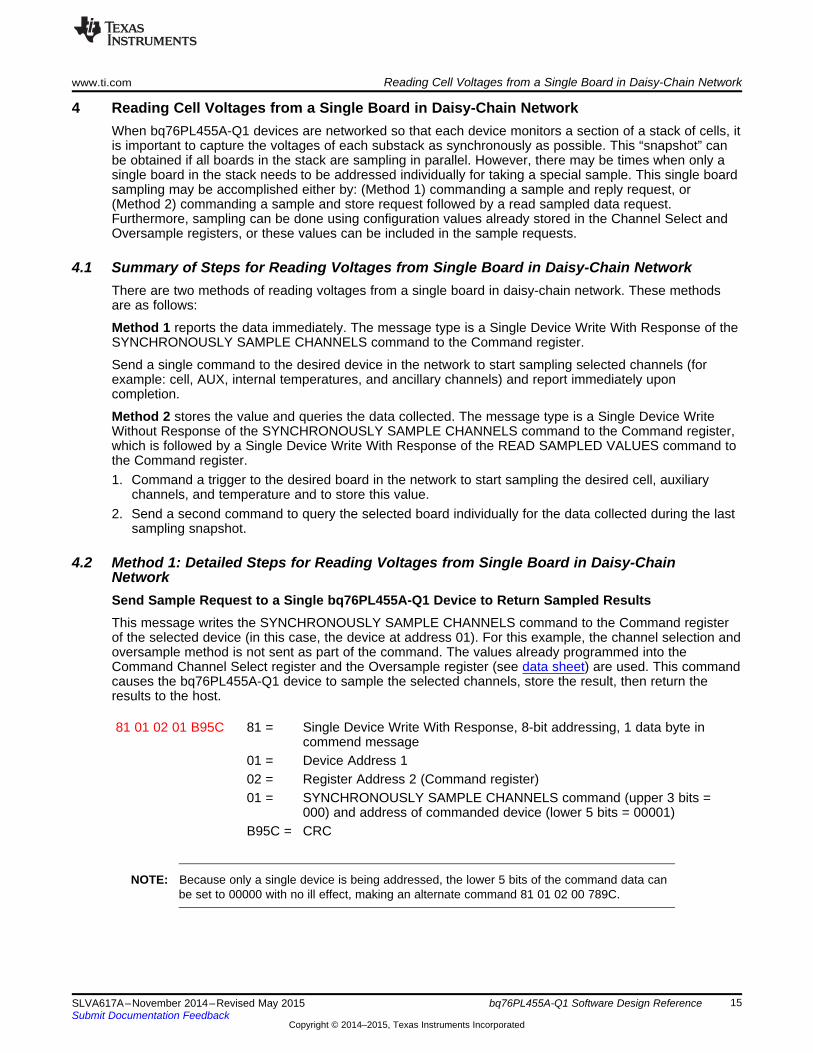
4.2 Method 1: Detailed Steps for Reading Voltages from Single Board in Daisy-ChainNetworkSend Sample Request to a Single bq76PL455A-Q1 Device to Return Sampled ResultsThis message writes the SYNCHRONOUSLY SAMPLE CHANNELS command to the Command registerof the selected device (in this case, the device at address 01). For this example, the channel selection andoversample method is not sent as part of the command. The values already programmed into theCommand Channel Select register and the Oversample register (see data sheet) are used. This commandcauses the bq76PL455A-Q1 device to sample the selected channels, store the result, then return theresults to the host.
81 01 02 01 B95C 81 = Single Device Write With Response, 8-bit addressing, 1 data byte incommend message
01 = Device Address 102 = Register Address 2 (Command register)01 = SYNCHRONOUSLY SAMPLE CHANNELS command (upper 3 bits =
000) and address of commanded device (lower 5 bits = 00001)B95C = CRC
NOTE: Because only a single device is being addressed, the lower 5 bits of the command data canbe set to 00000 with no ill effect, making an alternate command 81 01 02 00 789C.
15SLVA617A–November 2014–Revised May 2015 bq76PL455A-Q1 Software Design ReferenceSubmit Documentation Feedback
Copyright © 2014–2015, Texas Instruments Incorporated
Reading Cell Voltages from a Single Board in Daisy-Chain Network www.ti.com
0F 7473 7465 7483 7462 7471 7474 7477 745A ED34 (response)The example response message here assumes the commanded device had eightchannels selected for sampling. If the eight selected channels were cell channels1 through 8, then the first data would be for channel 8, then channel 7, and soforth.0F = Response Header (16 data bytes to follow; the value is always one less
than the number of data bytes)7473 = Channel 8 data7465 = Channel 7 data7483 = Channel 6 data7462 = Channel 5 data7471 = Channel 4 data7474 = Channel 3 data7477 = Channel 2 data745A = Channel 1 dataED34 = CRC
The example response message here assumes the commanded device had eight channels selected forsampling. If the eight selected channels were cell channels 1 through 8, then the first data would be forchannel 8, then channel 7, and so forth.
4.3 Method 2: Detailed Steps for Reading Voltages from Single Board in Daisy-ChainNetwork
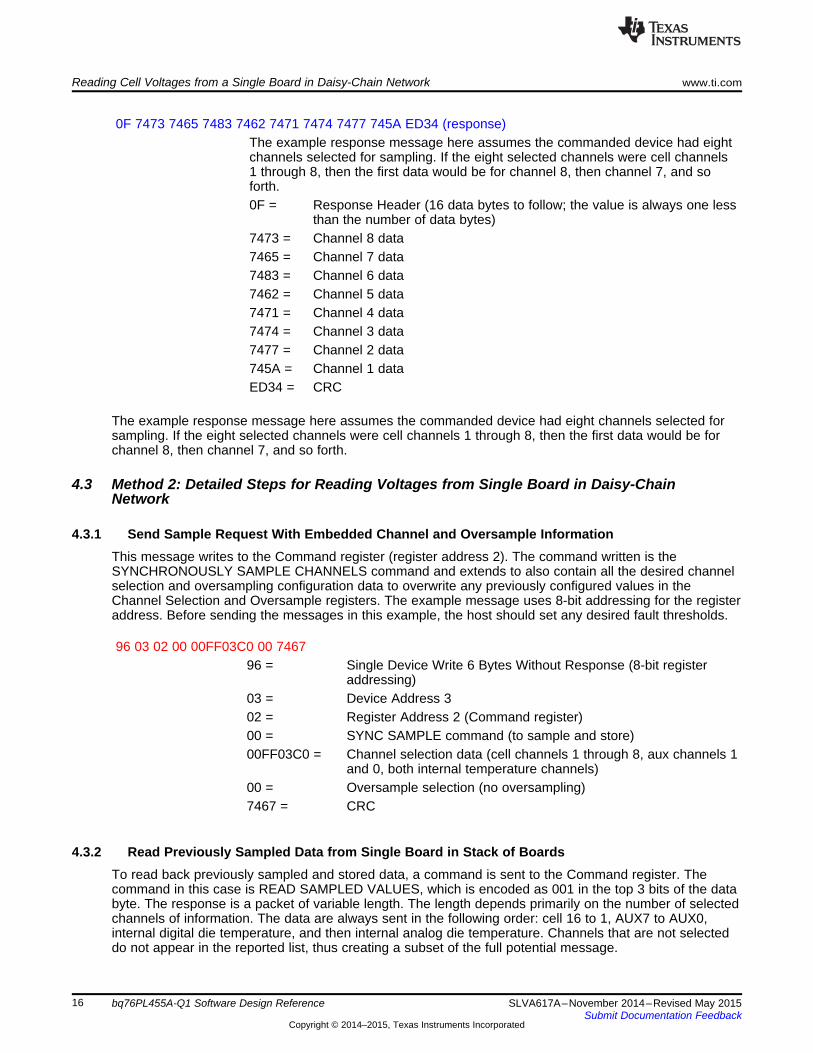
4.3.1 Send Sample Request With Embedded Channel and Oversample InformationThis message writes to the Command register (register address 2). The command written is theSYNCHRONOUSLY SAMPLE CHANNELS command and extends to also contain all the desired channelselection and oversampling configuration data to overwrite any previously configured values in theChannel Selection and Oversample registers. The example message uses 8-bit addressing for the registeraddress. Before sending the messages in this example, the host should set any desired fault thresholds.
96 03 02 00 00FF03C0 00 746796 = Single Device Write 6 Bytes Without Response (8-bit register
addressing)03 = Device Address 302 = Register Address 2 (Command register)00 = SYNC SAMPLE command (to sample and store)00FF03C0 = Channel selection data (cell channels 1 through 8, aux channels 1
and 0, both internal temperature channels)00 = Oversample selection (no oversampling)7467 = CRC
4.3.2 Read Previously Sampled Data from Single Board in Stack of BoardsTo read back previously sampled and stored data, a command is sent to the Command register. Thecommand in this case is READ SAMPLED VALUES, which is encoded as 001 in the top 3 bits of the databyte. The response is a packet of variable length. The length depends primarily on the number of selectedchannels of information. The data are always sent in the following order: cell 16 to 1, AUX7 to AUX0,internal digital die temperature, and then internal analog die temperature. Channels that are not selecteddo not appear in the reported list, thus creating a subset of the full potential message.
16 bq76PL455A-Q1 Software Design Reference SLVA617A–November 2014–Revised May 2015Submit Documentation Feedback
Copyright © 2014–2015, Texas Instruments Incorporated

www.ti.com Reading Cell Voltages from a Single Board in Daisy-Chain Network
81 03 02 20 D884 81 = Single Device Write With Response (8-bit register addressing)03 = Device Address 302 = Register Address 220 = READ SAMPLED VALUES commandD884 = CRC
17 AE54 85BC AE5A 8598 AE4F 8594 AE60 8514 FFF7 FFF7 82C4 64EC 5B7C (response)The response message here contains data for the previously selected andsampled channels from device at address 3 (as sampled using the command inSection 4.3.1). For a detailed break-down of a similar message, see Section 3.3.2.17 = Response Header byte (24 data bytes follow)AE54 = Channel 8 data85BC = Channel 7 dataAE5A = Channel 6 data8598 = Channel 5 dataAE4F = Channel 4 data8594 = Channel 3 dataAE60 = Channel 2 data8514 = Channel 1 dataFFF7 = AUX1 dataFFF7 = AUX0 data8204 = Internal digital die temp data64EC = Internal analog die temp data5B7C = CRC
17SLVA617A–November 2014–Revised May 2015 bq76PL455A-Q1 Software Design ReferenceSubmit Documentation Feedback
Copyright © 2014–2015, Texas Instruments Incorporated
Configuring and Using GPIO Pins www.ti.com
5 Configuring and Using GPIO PinsThe bq76PL455A-Q1 devices have General Purpose Input and Output (GPIO) pins. These GPIO pins canbe configured either as input or output pins, and each pin has its own internal pullup or pulldown that canbe enabled by writing to special control registers. There is no internal circuitry to automatically disablepullups when pulldowns are enabled, or vice versa, so be mindful of potential conflicts when configuringthe GPIO pins.
NOTE: GPIO[4..0] can be used to set the address of the bq76PL455A-Q1 device, if auto-addressmode is not selected. This function is controlled by the ADDR_SEL bit in the DeviceConfiguration register (address 14). Take care during design to avoid conflicting uses for theGPIO pins.
The registers associated with GPIO use are:• General Purpose I/O Direction (register address 120)• General Purpose Output (register address 121)• General Purpose Pullup (register address 122)• General Purpose Pulldown (register address 123)• General Purpose Input (register address 124)• General Purpose Fault Input (register address 125)
The GPIO pins can be configured to register faults, when an input applied to one or more of the pins is ata specified logic level. The level (high or low) used to trigger the fault can be programmed using theGeneral Purpose Fault Input register; the GPIO pins, which are included in the fault triggering mechanism,can also be selected using this register. By default, the fault generation mechanism associated with theGPIO pins is disabled. Once enabled, the faults are registered in the GPI Fault register (address 99). Aregistered fault on any of the GPIO pins can be included in the FAULT pin output by setting theGPI_FAULT_OUT bit in the Fault Output Control register (address 110 to 111).
5.1 Summary of Steps for Configuring and Using GPIO Pins1. Select pullups and pulldowns as defined for application (by default, no pullups nor pulldowns are
enabled).2. Select GPIO input or output configuration.3. Set the desired patterns to GPIO pins (or read input values). Examples:
(a) 001000(b) 010000(c) 100000(d) 111000(e) 000000
Steps 1 and 2 (in Section 5.1) may be reversed depending on pre-existing conditions in the configurationregisters and signals applied to the pins. In some cases it is better to disable all pullups and pulldowns,reconfigure the ports, then reenable any desired pullups and pulldowns.
The default values for the GPIO registers are:
General Purpose I/O Direction 00General Purpose Output 00General Purpose Pullup 00General Purpose Pulldown 00General Purpose Input xx (depends on input applied to pins)General Purpose Input Fault 00 (all GPI fault inputs disabled)
18 bq76PL455A-Q1 Software Design Reference SLVA617A–November 2014–Revised May 2015Submit Documentation Feedback
Copyright © 2014–2015, Texas Instruments Incorporated

www.ti.com Configuring and Using GPIO Pins
5.2 Detailed Steps for Configuring and Using GPIO Pins
5.2.1 Configure GPIO Pin Direction and Set New Pin ValuesFollowing is a sequence of example messages to configure the GPIO pins on the bottom (that is, address0) bq76PL455A-Q1 device, select pullups, and set output values. Eight-bit register addressing is used forall command messages.
Example messages (all values in hexadecimal):
91 00 7B 00 0E0C Turn off all pulldowns91 = Single Device Write Without Response (8-bit register addressing)00 = Device Address 07B = Register Address 123 (General Purpose Pulldown register)00 = Data (all pulldowns disabled)0E0C = CRC
91 00 7A 00 0F9C Turn off all pullups91 = Single Device Write Without Response (8-bit register addressing)00 = Device Address 07A = Register Address 122 (General Purpose Pullup register)00 = Data (all pullups disabled)0F9C = CRC
91 00 78 07 4F3E Configure GPIO[2..0] as outputs (and GPIO[5..3] as inputs)91 = Single Device Write Without Response (8-bit register addressing)00 = Device Address 078 = Register Address 120 (General Purpose I/O Direction register)07 = Data (set bits are output, cleared bits are input for bits 0 through 5)4F3E = CRC
91 00 7A 07 4E5E Turn on pullups on GPIO[2..0]91 = Single Device Write Without Response (8-bit register addressing)00 = Device Address 07A = Register Address 122 (General Purpose Pullup register)07 = Data (pullups disabled on GPIO[5..4], pullups enabled on GPIO[2..0])4E5E = CRC
91 00 79 01 CEAC Post pattern 001 to GPIO[2..0]91 = Single Device Write Without Response (8-bit register addressing)00 = Device Address 079 = Register Address 121 (General Purpose Output register)01 = Data (GPIO[0] = 1, all others = 0)CEAC = CRC
91 00 79 02 8EAD Post pattern 010 to GPIO[2..0]91 = Single Device Write Without Response (8-bit register addressing)00 = Device Address 079 = Register Address 121 (General Purpose Output register)02 = Data (GPIO[1] = 1, all others = 0)8EAD = CRC
19SLVA617A–November 2014–Revised May 2015 bq76PL455A-Q1 Software Design ReferenceSubmit Documentation Feedback
Copyright © 2014–2015, Texas Instruments Incorporated
Configuring and Using GPIO Pins www.ti.com
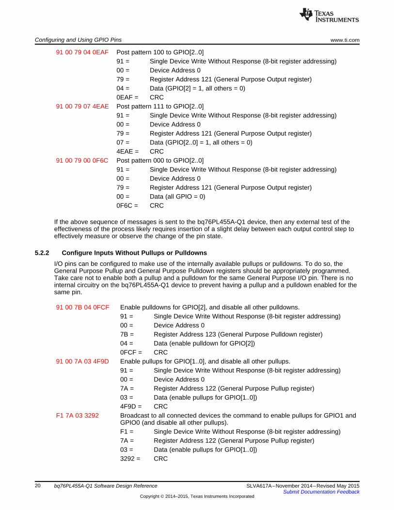
91 00 79 04 0EAF Post pattern 100 to GPIO[2..0]91 = Single Device Write Without Response (8-bit register addressing)00 = Device Address 079 = Register Address 121 (General Purpose Output register)04 = Data (GPIO[2] = 1, all others = 0)0EAF = CRC
91 00 79 07 4EAE Post pattern 111 to GPIO[2..0]91 = Single Device Write Without Response (8-bit register addressing)00 = Device Address 079 = Register Address 121 (General Purpose Output register)07 = Data (GPIO[2..0] = 1, all others = 0)4EAE = CRC
91 00 79 00 0F6C Post pattern 000 to GPIO[2..0]91 = Single Device Write Without Response (8-bit register addressing)00 = Device Address 079 = Register Address 121 (General Purpose Output register)00 = Data (all GPIO = 0)0F6C = CRC
If the above sequence of messages is sent to the bq76PL455A-Q1 device, then any external test of theeffectiveness of the process likely requires insertion of a slight delay between each output control step toeffectively measure or observe the change of the pin state.
5.2.2 Configure Inputs Without Pullups or PulldownsI/O pins can be configured to make use of the internally available pullups or pulldowns. To do so, theGeneral Purpose Pullup and General Purpose Pulldown registers should be appropriately programmed.Take care not to enable both a pullup and a pulldown for the same General Purpose I/O pin. There is nointernal circuitry on the bq76PL455A-Q1 device to prevent having a pullup and a pulldown enabled for thesame pin.
91 00 7B 04 0FCF Enable pulldowns for GPIO[2], and disable all other pulldowns.91 = Single Device Write Without Response (8-bit register addressing)00 = Device Address 07B = Register Address 123 (General Purpose Pulldown register)04 = Data (enable pulldown for GPIO[2])0FCF = CRC
91 00 7A 03 4F9D Enable pullups for GPIO[1..0], and disable all other pullups.91 = Single Device Write Without Response (8-bit register addressing)00 = Device Address 07A = Register Address 122 (General Purpose Pullup register)03 = Data (enable pullups for GPIO[1..0])4F9D = CRC
F1 7A 03 3292 Broadcast to all connected devices the command to enable pullups for GPIO1 andGPIO0 (and disable all other pullups).F1 = Single Device Write Without Response (8-bit register addressing)7A = Register Address 122 (General Purpose Pullup register)03 = Data (enable pullups for GPIO[1..0])3292 = CRC
20 bq76PL455A-Q1 Software Design Reference SLVA617A–November 2014–Revised May 2015Submit Documentation Feedback
Copyright © 2014–2015, Texas Instruments Incorporated

www.ti.com Configuring and Using GPIO Pins
5.2.3 Write to General Purpose Outputs or Read from General Purpose Inputs
5.2.3.1 Setting an Output ValueThe General Purpose Output Bits for GPIO[5..0] are encoded into the lower 6 bits of the General PurposeOutput register. General purpose output 0 is controlled by bit 0, general purpose output 1 is controlled bybit 1, and so on. The value of the General Purpose Output pin follows the bit setting in the correspondingregister bit. If a bit in the General Purpose Output register is cleared (written to 0), the correspondinggeneral purpose output pin is driven low. If the register bit is set (written to 1), the corresponding generalpurpose output pin is driven high. Before setting new values on the general purpose outputs, the desiredinput or output direction should be set for the input or output ports by writing to the General Purpose I/ODirection register.
91 00 78 17 4EF2 Configure GPIO[4] and GPIO[2..0] as output, and GPIO[3] and GPIO[5] as input91 = Write Without Response (8-bit register addressing)00 = Device Address 078 = Register Address 120 (General Purpose I/O Direction register)17 = Data4EF2 = CRC
91 00 79 12 8F61 Set GPIO[4] and GPIO[1], clear GPIO[2] and GPIO[0]91 = Single Device Write Without Response (8-bit register addressing)00 = Device Address 079 = Register Address 121 (General Purpose Output register)12 = Data8F61 = CRC
5.2.3.2 Reading an Input Value
91 01 78 30 5F28 Make GPIO[4..5] output and GPIO[3..0] input91 = Single Device Write Without Response (8-bit register addressing)01 = Device Address 178 = Register Address 120 (General Purpose I/O Direction register)30 = Data5F28 = CRC
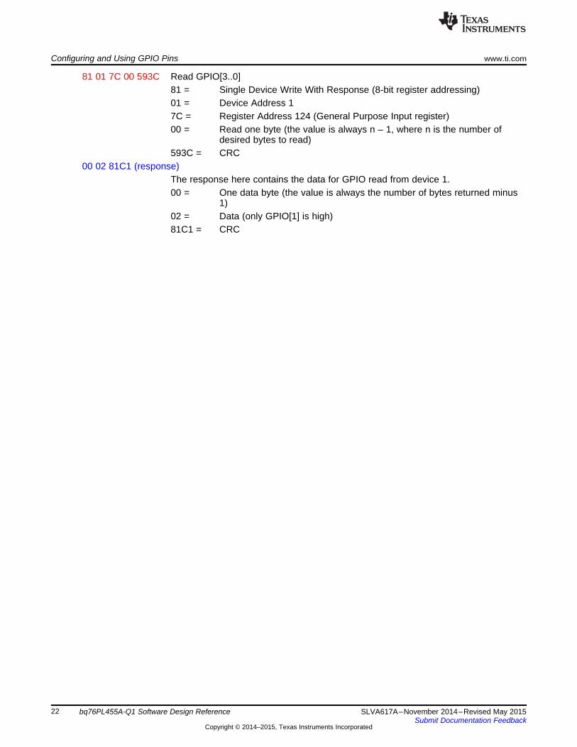
81 01 7C 00 593C Read GPIO[3..0] (since GPIO[4..5] are configured as output)81 = Single Device Write With Response (read) (8-bit register addressing)01 = Device Address 17C = Register Address 124 (General Purpose Input register)00 = Read 1 byte (value is always n – 1, where n is the number of desired
bytes to read)593C = CRC
00 07 41C2 (response)This response contains the data for GPIO read from device 1.00 = One data byte (the value is always the number of bytes returned minus
1)07 = Data (GPIO[2..0] = high, others = low)41C2 = CRC
(Delay, externally apply different input to GPIO pins, then read the GPIO pinsagain)
21SLVA617A–November 2014–Revised May 2015 bq76PL455A-Q1 Software Design ReferenceSubmit Documentation Feedback
Copyright © 2014–2015, Texas Instruments Incorporated
Configuring and Using GPIO Pins www.ti.com
81 01 7C 00 593C Read GPIO[3..0]81 = Single Device Write With Response (8-bit register addressing)01 = Device Address 17C = Register Address 124 (General Purpose Input register)00 = Read one byte (the value is always n – 1, where n is the number of
desired bytes to read)593C = CRC
00 02 81C1 (response)The response here contains the data for GPIO read from device 1.00 = One data byte (the value is always the number of bytes returned minus
1)02 = Data (only GPIO[1] is high)81C1 = CRC
22 bq76PL455A-Q1 Software Design Reference SLVA617A–November 2014–Revised May 2015Submit Documentation Feedback
Copyright © 2014–2015, Texas Instruments Incorporated
www.ti.com Saving Register Configuration to EEPROM
6 Saving Register Configuration to EEPROMAt powerup, the bq76PL455A-Q1 device transfers the contents of registers in EEPROM to registers inRAM. This sets the initial register configuration. One can then modify the registers to a specificconfiguration useful for a specific application. If power is removed from the device, this new configurationis lost, unless it is saved back to EEPROM. To protect against inadvertently setting an undesired deviceconfiguration, a specific sequence of events is required to save register values to EEPROM.
CAUTIONEEPROM can only be written a limited number of times, so use this procedurewith great care.
6.1 Summary of Steps for Saving Register Configuration to EEPROMThe following steps are required to save register values to EEPROM:1. Write Magic Number 1.2. Write Magic Number 2.3. Save register values to EEPROM.4. Wait until save of register values is complete.
The saving of data from RAM to EEPROM takes approximately 200 ms to complete. Take care to allowthe write to complete before accessing the information, powering down, or rewriting the register valuesanother time. The WRITE_EEPROM bit is cleared by hardware when the save is complete.
6.2 Detailed Steps for Saving Register Configuration to EEPROM
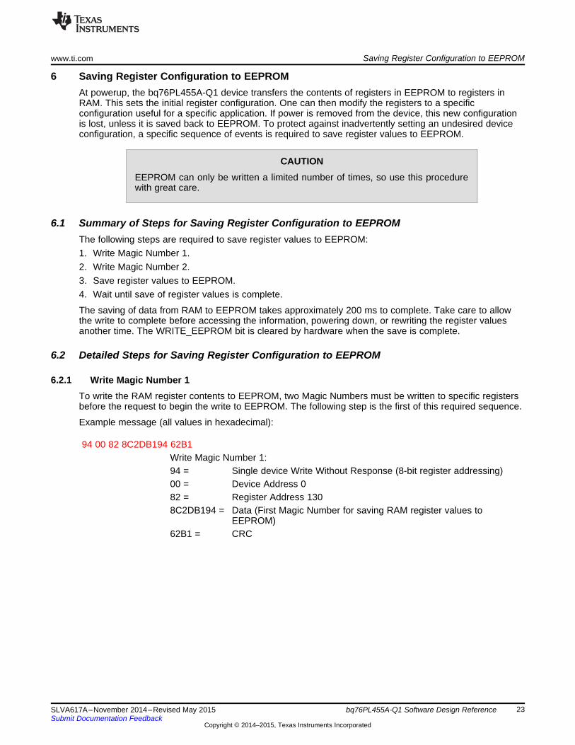
6.2.1 Write Magic Number 1To write the RAM register contents to EEPROM, two Magic Numbers must be written to specific registersbefore the request to begin the write to EEPROM. The following step is the first of this required sequence.
Example message (all values in hexadecimal):
94 00 82 8C2DB194 62B1Write Magic Number 1:94 = Single device Write Without Response (8-bit register addressing)00 = Device Address 082 = Register Address 1308C2DB194 = Data (First Magic Number for saving RAM register values to
EEPROM)62B1 = CRC
23SLVA617A–November 2014–Revised May 2015 bq76PL455A-Q1 Software Design ReferenceSubmit Documentation Feedback
Copyright © 2014–2015, Texas Instruments Incorporated

Saving Register Configuration to EEPROM www.ti.com
6.2.2 Write Magic Number 2To write the RAM register contents to EEPROM, two Magic Numbers must be written to specific registersbefore the request to begin writing to EEPROM. The following step is the second of this requiredsequence.
Example message (all values in hexadecimal):
94 00 FC A375E60F BC27Write Magic Number 2:94 = Single Device Write Without Response (8-bit register addressing)00 = Device Address 0FC = Register Address 252A375E60F = Data (Second Magic Number for saving RAM register values to
EEPROM)BC27 = CRC
6.2.3 Save Register Values to EEPROMWhen the Magic Number registers are programmed with the proper values, the save request can beinitiated by writing the WRITE_EEPROM bit in the Device Control register to 1. This action initiates theaction of saving register values from RAM registers to corresponding storage locations in EEPROM.
NOTE: Not all registers in RAM have a corresponding storage value in EEPROM. For a list of whichregisters are saved to EEPROM, see the register summary section of the data sheet.
Example messages (all values in hexadecimal):
91 00 0C 10 2830 Write RAM to EEPROM:91 = Single Device Write Without Response (8-bit register addressing)00 = Device Address 00C = Register Address 1210 = Data (set the WRITE_EEPROM bit in the Device Control register)2830 = CRC
6.2.4 Wait Until Save of Register Values is CompleteSaving register data from RAM to EEPROM completes in approximately 200 ms. Therefore, simplydelaying this amount of time is sufficient before relying on the EEPROM data. However, if it becomesnecessary to know specifically when the save completes, or if a verification of this save is required, thenthe WRITE_EEPROM bit in the Device Control register can be read. This bit writes to 1 to initiate the datasave, and is cleared to 0 by hardware to indicate the task is complete.
CAUTIONAllow this process to complete to avoid erroneous IC operation.
24 bq76PL455A-Q1 Software Design Reference SLVA617A–November 2014–Revised May 2015Submit Documentation Feedback
Copyright © 2014–2015, Texas Instruments Incorporated
www.ti.com Saving Register Configuration to EEPROM
Example messages (all values in hexadecimal):
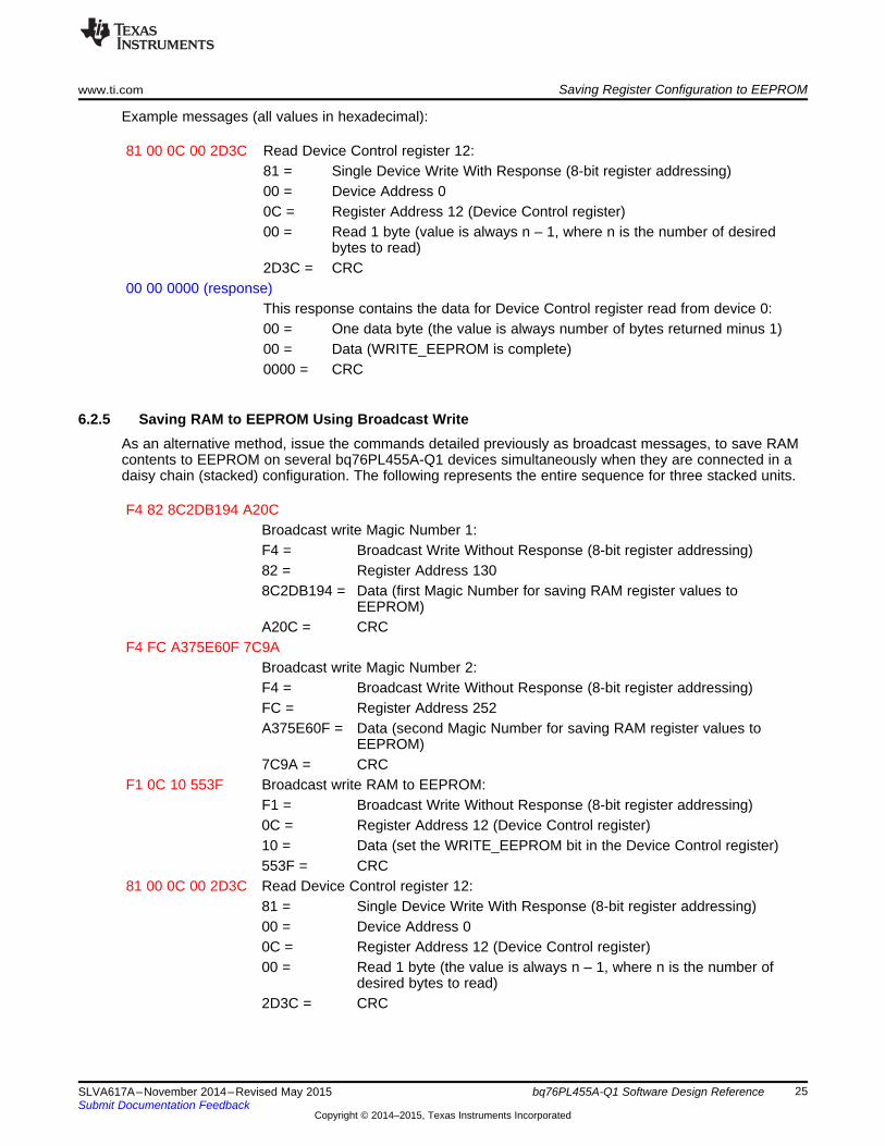
81 00 0C 00 2D3C Read Device Control register 12:81 = Single Device Write With Response (8-bit register addressing)00 = Device Address 00C = Register Address 12 (Device Control register)00 = Read 1 byte (value is always n – 1, where n is the number of desired
bytes to read)2D3C = CRC
00 00 0000 (response)This response contains the data for Device Control register read from device 0:00 = One data byte (the value is always number of bytes returned minus 1)00 = Data (WRITE_EEPROM is complete)0000 = CRC
6.2.5 Saving RAM to EEPROM Using Broadcast WriteAs an alternative method, issue the commands detailed previously as broadcast messages, to save RAMcontents to EEPROM on several bq76PL455A-Q1 devices simultaneously when they are connected in adaisy chain (stacked) configuration. The following represents the entire sequence for three stacked units.
F4 82 8C2DB194 A20CBroadcast write Magic Number 1:F4 = Broadcast Write Without Response (8-bit register addressing)82 = Register Address 1308C2DB194 = Data (first Magic Number for saving RAM register values to
EEPROM)A20C = CRC
F4 FC A375E60F 7C9ABroadcast write Magic Number 2:F4 = Broadcast Write Without Response (8-bit register addressing)FC = Register Address 252A375E60F = Data (second Magic Number for saving RAM register values to
EEPROM)7C9A = CRC
F1 0C 10 553F Broadcast write RAM to EEPROM:F1 = Broadcast Write Without Response (8-bit register addressing)0C = Register Address 12 (Device Control register)10 = Data (set the WRITE_EEPROM bit in the Device Control register)553F = CRC
81 00 0C 00 2D3C Read Device Control register 12:81 = Single Device Write With Response (8-bit register addressing)00 = Device Address 00C = Register Address 12 (Device Control register)00 = Read 1 byte (the value is always n – 1, where n is the number of
desired bytes to read)2D3C = CRC
25SLVA617A–November 2014–Revised May 2015 bq76PL455A-Q1 Software Design ReferenceSubmit Documentation Feedback
Copyright © 2014–2015, Texas Instruments Incorporated

Saving Register Configuration to EEPROM www.ti.com
00 00 0000 (response)This response contains the data for Device Control register read from device 0:00 = One data byte (the value is always the number of bytes returned
minus 1)00 = Data (WRITE_EEPROM is complete)0000 = CRC
81 01 0C 00 7CFC Read Device Control register 12:81 = Single Device Write With Response (8-bit register addressing)01 = Device Address 10C = Register Address 12 (Device Control register)00 = Read 1 byte (the value is always n – 1, where n is the number of
desired bytes to read)7CFC = CRC
00 00 0000 (response)This response contains the data for Device Control register read from device 0:00 = One data byte (the value is always the number of bytes returned
minus 1)00 = Data (WRITE_EEPROM is complete)0000 = CRC
81 02 0C 00 8CFC Read Device Control register 12:81 = Single Device Write With Response (8-bit register addressing)02 = Device Address 20C = Register Address 12 (Device Control register)00 = Read 1 byte (the value is always n – 1, where n is the number of
desired bytes to read)8CFC = CRC
00 00 0000 (response)This response contains the data for Device Control register read from device 0:00 = One data byte (the value is always the number of bytes returned
minus 1)00 = Data (WRITE_EEPROM is complete)0000 = CRC
26 bq76PL455A-Q1 Software Design Reference SLVA617A–November 2014–Revised May 2015Submit Documentation Feedback
Copyright © 2014–2015, Texas Instruments Incorporated
www.ti.com Group Broadcast Write With Response
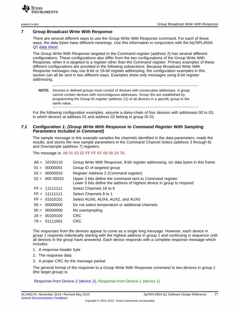
7 Group Broadcast Write With ResponseThere are several different ways to use the Group Write With Response command. For each of theseways, the data bytes have different meanings. Use this information in conjunction with the bq76PL455A-Q1 data sheet.
The Group Write With Response targeted to the Command register (address 2) has several differentconfigurations. These configurations also differ from the two configurations of the Group Write WithResponse, when it is targeted to a register other than the Command register. Primary examples of thesedifferent configurations are provided in the following subsections. Because Broadcast Write WithResponse messages may use 8-bit or 16-bit register addressing, the configuration examples in thissection can all be sent in two different ways. Examples show only messages using 8-bit registeraddressing.
NOTE: Devices in defined groups must consist of devices with consecutive addresses. A groupcannot contain devices with noncontiguous addresses. Group IDs are established byprogramming the Group ID register (address 11) of all devices in a specific group to thesame value.
For the following configuration examples, assume a daisy-chain of four devices with addresses 00 to 03,in which devices at address 01 and address 02 belong to group ID 01.
7.1 Configuration 1: (Group Write With Response to Command Register With SamplingParameters Included in Command)The sample message in this example samples the channels identified in the data parameters, reads theresults, and stores the new sample parameters in the Command Channel Select (address 3 through 6)and Oversample (address 7) registers.
The message is: A6 01 02 02 FF FF FF 00 00 24 79.
A6 = 10100110 Group Write With Response, 8-bit register addressing, six data bytes in this frame01 = 00000001 Group ID of targeted group02 = 00000010 Register Address 2 (Command register)02 = 000 00010 Upper 3 bits define the command sent to Command register
Lower 5 bits define the address of highest device in group to respondFF = 11111111 Select Channels 16 to 9FF = 11111111 Select Channels 8 to 1FF = 01010101 Select AUX6, AUX4, AUX2, and AUX000 = 00000000 Do not select temperature or additional channels00 = 00000000 No oversampling24 = 00100100 CRC79 = 01111001 CRC
The responses from the devices appear to come as a single long message. However, each device ingroup 1 responds individually starting with the highest address in group 1 and continuing in sequence untilall devices in the group have answered. Each device responds with a complete response message whichincludes:1. A response header byte2. The response data3. A proper CRC for the message packet
The general format of the response to a Group Write With Response command to two devices in group 1(the target group) is:
Response-from-Device-2 (device 2), Response-from-Device-1 (device 1)
27SLVA617A–November 2014–Revised May 2015 bq76PL455A-Q1 Software Design ReferenceSubmit Documentation Feedback
Copyright © 2014–2015, Texas Instruments Incorporated
Group Broadcast Write With Response www.ti.com
7.2 Configuration 2: (Group Write With Response to Command Register WithoutSampling Parameters Included in Command – Sampling Parameters are Taken fromValues Already Stored in the Command Channel Select and Oversampling Registers)The sample message in this example samples the channels identified by the values currently stored in theCommand Channel Select register (address 3 through 6) by using the oversample setting currently set inthe Oversample register (address 7).
The message is: A1 01 02 02 F2 9D.
A1 = 1010 0 001 Group Write With Response, 8-bit register addressing, 1 data byte in this frame01 = 00000001 Group ID of targeted group02 = 00000010 Register Address 2 (Command register)02 = 000 00010 Upper 3 bits define the command sent to Command register
Lower 5 bits define the address of highest device in group to respondF2 = 11110010 CRC9D = 10011101 CRC
As in the response for the command message described in Section 7.1, the responses from the devices ingroup 1 appear to come as a single long message. However, each device in group 1 respondsindividually, starting with the device at the highest address in the group and continues in sequence to thenext lower address until all devices in group 1 have answered. Each device responds with a completeresponse message which includes:1. A response header byte2. The response data3. A proper CRC for the message packet
The general format for the chained messages in response to a Group Write With Response command tothe two group 1 devices is:
Response-from-Device-2 (device 2), Response-from-Device-1 (device 1)
See Section 3 and Section 4 for an example of the data format of an individual response to a channelconversion request. That section describes the response of an individual device byte-by-byte.
7.3 Configuration 3: (Group Write With Response to Non-Command Register Using 2Bytes for Addressing and Response Size)The sample command message in this example should generate a response from the two devicesbelonging to group 1. Each device response contains the value currently stored in its Command ChannelSelect (address 3 through 6) register.
The message is: A2 01 03 02 03 49 44.
A2 = 10100010 Group Write With Response, 8-bit register addressing, 2 data bytes in this frame01 = 00000001 Group ID of targeted group03 = 00000011 Register Address (the Command Channel Select register)02 = 00000010 Address of highest device in group to respond03 = 00000011 Number of data bytes minus 1 expected in response (4 bytes in this example)49 = 01001001 CRC44 = 01000100 CRC
For the purpose of this example, assume the devices in group 1 being queried (at addresses 02 and 01)have the following contents in the Command Channel Select register (address 3 through 6):
28 bq76PL455A-Q1 Software Design Reference SLVA617A–November 2014–Revised May 2015Submit Documentation Feedback
Copyright © 2014–2015, Texas Instruments Incorporated
www.ti.com Group Broadcast Write With Response
Device at address 1: FFFF0000 (All cell channels and no AUX channels)Device at address 2: FFFF0100 (All cell channels and AUX0)
If this is the case, then the response message to the Group Write With Response command query aboveis:
03 FF FF 01 00 45 B4 03 FF FF 00 00 44 24 (response)
Although this message initially looks as though it is a single message, it is actually comprised of twoseparate messages, one from each of the two queried devices. Parenthetical text after the messageprovides further insight. The first response message is from the device at address 2 (listed first) and thesecond response message is from the device at address 1 (listed second).
03 FF FF 01 00 45 B4 (device 2), 03 FF FF 00 00 44 24 (device 1)
This ordering of response messages (from highest address to lowest address) is the same for anyresponse to a Group Write With Response command message. First, the response from the device at the(highest) address specified in the group by the command message occurs, followed by the next loweraddress, and so forth until all devices in the designated group have responded.
Each response message has the same format. Breaking down the response message from the device ataddress 2 from the group of responses yields the following message structure:
The message is: 03 FF FF 01 00 45 B4 (response).
03 = 0 0000011 Response frame, 4 data bytes in this frameFF = 11111111 First data byte: cell channels 16 through 9 selectedFF = 11111111 Second data byte: cell channels 8 through 1 selected01 = 00000001 Third data byte: AUX0 selected00 = 00000000 Fourth data byte: no additional channels selected45 = 01000101 CRCB4 = 10110100 CRC
7.4 Configuration 4: (Group Write With Response to Non-Command Register Using 1Byte for Addressing and Response Size)As in the example for Section 7.3, the sample message in this example reads the value currently stored inthe Command Channel Select (address 3 through 6) register, but the message to do so is one byteshorter.
The message is: A1 01 03 62 F3 25.
A1 = 1010 0 001 Group Write With Response, 8-bit register addressing, 1 data byte in this frame01 = 00000001 Group ID of targeted group03 = 00000011 Register Address62 = 011 00010 Upper 3 bits are Number of Data Bytes minus 1 expected in response
Lower 5 bits define the address of highest device in group to respondF3 = 11110011 CRC25 = 00100101 CRC
29SLVA617A–November 2014–Revised May 2015 bq76PL455A-Q1 Software Design ReferenceSubmit Documentation Feedback
Copyright © 2014–2015, Texas Instruments Incorporated

Group Broadcast Write With Response www.ti.com
For this example, assuming the same conditions provided for the example in Section 7.3, the responsesare identical. In the following response message, the part of the response message starting with 03 andending with B4 is from the device at address 2. The part of the response message starting with 03 andending with 24 is from the device at address 1.
03 FF FF 01 00 45 B4 (device 2), 03 FF FF 00 00 44 24 (device 1)
For an explanation of the breakdown of the response packet, see the Section 7.3 example.
NOTE: Each of these configurations can also be modified to use 16-bit register addressing, whichwould add an additional byte to the message frame.
30 bq76PL455A-Q1 Software Design Reference SLVA617A–November 2014–Revised May 2015Submit Documentation Feedback
Copyright © 2014–2015, Texas Instruments Incorporated
www.ti.com General Broadcast Write With Response
8 General Broadcast Write With ResponseThere are two methods in which a Broadcast Write With Response can be implemented. One of themethods uses 1 byte to specify both the address of the highest board in the response chain and thenumber of desired response bytes. The other method uses 2 bytes to specify the address of the highestresponding device and the desired number of response bytes separately (first the address, then thenumber of bytes minus 1).
Both methods can use either 16-bit register addressing or 8-bit register addressing, depending on thesetting in the header byte of the command message packet. The following examples use 16-bit registeraddressing. The responses would be the same independent of the register addressing method specified inthe command header byte.
8.1 Configuration 1: (2-Byte Addressing Method)The following is an example of the 2-byte method (to read the Command Channel Select register fromthree devices).
The message is: EA 00 03 02 03 A8 B6.
EA = 1110 1 010 Broadcast Write With Response, 16-bit register addressing, 2 data bytes in thisframe (first contains the highest address to respond, second contains the expecteddata bytes minus 1 from each device expected to respond)
00 = 00000000 MSB of register address is 0003 = 00000011 LSB of register address is 0302 = 00000010 Address of highest (first) device to respond03 = 00000011 Number of data bytes minus 1 expected in response (that is, 4 bytes)A8 = 10101000 CRCB6 = 10110110 CRC
For the purpose of this example, assume the three devices being queried (at addresses 02, 01, and 00)have the following contents in register 3:
Device at address 0: FFFFFF00 All cell channels and all AUX channelsDevice at address 1: FFFF0000 All cell channels and no AUX channelsDevice at address 2: FFFF0100 All cell channels and AUX0
If this is the case, then the response message to the command query above is:
03 FF FF 01 00 45 B4 03 FF FF 00 00 44 24 03 FF FF FF 00 05 D4 (response)
Although this message initially looks as though it is a single message, it is actually comprised of threeseparate messages, one from each of the three queried devices. Parenthetical text after the messageprovides further insight. The first response message is from the device at address 2, the second responsemessage is from the device at address 1, and the third response message is from the device at address 0.This ordering of response messages (from highest address to lowest address) is the same for anyresponse to a Broadcast Write With Response command message: the response from the device at the(highest) address specified in the command message responds first, followed by the next lower address,and so forth until all devices have responded.
03 FF FF 01 00 45 B4 (device 2), 03 FF FF 00 00 44 24 (device 1), 03 FF FF FF 00 05 D4 (device 0)
31SLVA617A–November 2014–Revised May 2015 bq76PL455A-Q1 Software Design ReferenceSubmit Documentation Feedback
Copyright © 2014–2015, Texas Instruments Incorporated
General Broadcast Write With Response www.ti.com
Each response message has the same format. Breaking down the response message from the device ataddress 2 from the group of responses yields the following message structure:
The message is: 03 FF FF 01 00 45 B4 (device 2).
03 = 0 0000011 Response frame, 4 data bytes in this frameFF = 11111111 First data byte: cell channels 16 through 9 selectedFF = 11111111 Second data byte: cell channels 8 through 1 selected01 = 00000001 Third data byte: AUX0 selected00 = 00000000 Fourth data byte: no additional channels selected45 = 01000101 CRCB4 = 10110100 CRC
8.2 Configuration 2: (1-Byte Addressing Method)The following 1-byte method example produces the same result as in the preceding 2-byte example.
The message is: E9 00 03 62 B5 45.
E9 = 1110 1 001 Broadcast Write With Response, 16-bit register addressing, 1 data byte in thisframe
00 = 00000000 MSB of register address03 = 00000011 LSB of register address62 = 011 00010 Upper 3 bits (011) are number of data bytes minus 1 expected in response from
each responding deviceLower 5 bits (00010) represent the address of highest device to respond
B5 = 10110101 CRC45 = 01000101 CRC
For this example, assuming the same conditions provided in the Section 7.1 example, the responses areidentical. In the following response message, the part of the response message starting with 03 andending with B4, is from the device at address 2; the part of the response message starting with 03 andending with 24, is from the device at address 1; and the part of the response message starting with 03and ending with D4, is from the device at address 0.
03 FF FF 01 00 45 B4 (device 2), 03 FF FF 00 00 44 24 (device 1), 03 FF FF FF 00 05 D4 (device 0)
For an explanation of the breakdown of the response packet, see the example in Section 8.1.
Revision History
Changes from Original (November 2014) to A Revision ................................................................................................ Page
• Changed document title .................................................................................................................. 1• Changed part number to bq76PL455A-Q1 ............................................................................................ 1• Changed data manual to data sheet, SLUSC51 ...................................................................................... 1• Changed sampling period value......................................................................................................... 7• Changed changed data value to BC and description to 60.04 µs for cell sampling period and 99.92 µs for internal
temperature sampling period ........................................................................................................... 7• Changed CRC to 9CED .................................................................................................................. 7
NOTE: Page numbers for previous revisions may differ from page numbers in the current version.
32 Revision History SLVA617A–November 2014–Revised May 2015Submit Documentation Feedback
Copyright © 2014–2015, Texas Instruments Incorporated

IMPORTANT NOTICE
Texas Instruments Incorporated and its subsidiaries (TI) reserve the right to make corrections, enhancements, improvements and otherchanges to its semiconductor products and services per JESD46, latest issue, and to discontinue any product or service per JESD48, latestissue. Buyers should obtain the latest relevant information before placing orders and should verify that such information is current andcomplete. All semiconductor products (also referred to herein as “components”) are sold subject to TI’s terms and conditions of salesupplied at the time of order acknowledgment.TI warrants performance of its components to the specifications applicable at the time of sale, in accordance with the warranty in TI’s termsand conditions of sale of semiconductor products. Testing and other quality control techniques are used to the extent TI deems necessaryto support this warranty. Except where mandated by applicable law, testing of all parameters of each component is not necessarilyperformed.TI assumes no liability for applications assistance or the design of Buyers’ products. Buyers are responsible for their products andapplications using TI components. To minimize the risks associated with Buyers’ products and applications, Buyers should provideadequate design and operating safeguards.TI does not warrant or represent that any license, either express or implied, is granted under any patent right, copyright, mask work right, orother intellectual property right relating to any combination, machine, or process in which TI components or services are used. Informationpublished by TI regarding third-party products or services does not constitute a license to use such products or services or a warranty orendorsement thereof. Use of such information may require a license from a third party under the patents or other intellectual property of thethird party, or a license from TI under the patents or other intellectual property of TI.Reproduction of significant portions of TI information in TI data books or data sheets is permissible only if reproduction is without alterationand is accompanied by all associated warranties, conditions, limitations, and notices. TI is not responsible or liable for such altereddocumentation. Information of third parties may be subject to additional restrictions.Resale of TI components or services with statements different from or beyond the parameters stated by TI for that component or servicevoids all express and any implied warranties for the associated TI component or service and is an unfair and deceptive business practice.TI is not responsible or liable for any such statements.Buyer acknowledges and agrees that it is solely responsible for compliance with all legal, regulatory and safety-related requirementsconcerning its products, and any use of TI components in its applications, notwithstanding any applications-related information or supportthat may be provided by TI. Buyer represents and agrees that it has all the necessary expertise to create and implement safeguards whichanticipate dangerous consequences of failures, monitor failures and their consequences, lessen the likelihood of failures that might causeharm and take appropriate remedial actions. Buyer will fully indemnify TI and its representatives against any damages arising out of the useof any TI components in safety-critical applications.In some cases, TI components may be promoted specifically to facilitate safety-related applications. With such components, TI’s goal is tohelp enable customers to design and create their own end-product solutions that meet applicable functional safety standards andrequirements. Nonetheless, such components are subject to these terms.No TI components are authorized for use in FDA Class III (or similar life-critical medical equipment) unless authorized officers of the partieshave executed a special agreement specifically governing such use.Only those TI components which TI has specifically designated as military grade or “enhanced plastic” are designed and intended for use inmilitary/aerospace applications or environments. Buyer acknowledges and agrees that any military or aerospace use of TI componentswhich have not been so designated is solely at the Buyer's risk, and that Buyer is solely responsible for compliance with all legal andregulatory requirements in connection with such use.TI has specifically designated certain components as meeting ISO/TS16949 requirements, mainly for automotive use. In any case of use ofnon-designated products, TI will not be responsible for any failure to meet ISO/TS16949.
Products ApplicationsAudio www.ti.com/audio Automotive and Transportation www.ti.com/automotiveAmplifiers amplifier.ti.com Communications and Telecom www.ti.com/communicationsData Converters dataconverter.ti.com Computers and Peripherals www.ti.com/computersDLP® Products www.dlp.com Consumer Electronics www.ti.com/consumer-appsDSP dsp.ti.com Energy and Lighting www.ti.com/energyClocks and Timers www.ti.com/clocks Industrial www.ti.com/industrialInterface interface.ti.com Medical www.ti.com/medicalLogic logic.ti.com Security www.ti.com/securityPower Mgmt power.ti.com Space, Avionics and Defense www.ti.com/space-avionics-defenseMicrocontrollers microcontroller.ti.com Video and Imaging www.ti.com/videoRFID www.ti-rfid.comOMAP Applications Processors www.ti.com/omap TI E2E Community e2e.ti.comWireless Connectivity www.ti.com/wirelessconnectivity
Mailing Address: Texas Instruments, Post Office Box 655303, Dallas, Texas 75265Copyright © 2015, Texas Instruments Incorporated