Embed Size (px)
Citation preview

BQ2404x 1A, Single-Input, Single Cell Li-Ion and Li-Pol Battery Charger With AutoStart
1 Features• Charging
– 1% Charge voltage accuracy– 10% Charge current accuracy– Pin selectable USB 100 mA and 500 mA
maximum input current limit– Programmable termination and precharge
threshold, BQ24040 and BQ24045– High voltage (4.35 V) chemistry support with
BQ24045• Protection
– 30V Input rating; with 6.6 V or 7.1 V inputovervoltage protection
– Input voltage dynamic power management– 125°C thermal regulation; 150°C thermal
shutdown protection– OUT Short-circuit protection and ISET short
detection– Operation over JEITA range via battery NTC –
1/2 fast-charge-current at Cold, 4.06V at Hot,BQ24040 and BQ24045
– Fixed 10 hour safety timer, BQ24040 andBQ24045
• System– Automatic termination and timer disable mode
(TTDM) for absent battery pack with thermistor,BQ24040 and BQ24045
– Status indication – charging and done– Available in small 2 × 2 mm2 DFN-10 package– Integrated auto start function for production line
testing, BQ24041• Functional Safety-Capable (BQ24040)
– Documentation available to aid functional safetysystem design
• Safety-Related Certifications:– IEC 62368-1 CB Certification (BQ24040,
BQ24045)
2 Applications• TWS Headsets and headphones• Smartwatches and wristbands• Wireless speakers• Mobile POS• Portable medical devices
3 DescriptionThe BQ2404x series of devices are highly integratedLi-Ion and Li-Pol linear chargers devices targeted atspace-limited portable applications. The devicesoperate from either a USB port or AC adapter. Thehigh input voltage range with input overvoltageprotection supports low-cost unregulated adapters.
The BQ2404x has a single power output that chargesthe battery. A system load can be placed in parallelwith the battery as long as the average system loaddoes not keep the battery from charging fully duringthe 10 hour safety timer.
The battery is charged in three phases: conditioning,constant current and constant voltage. In all chargephases, an internal control loop monitors the ICjunction temperature and reduces the charge currentif an internal temperature threshold is exceeded.
The charger power stage and charge current sensefunctions are fully integrated. The charger functionhas high accuracy current and voltage regulationloops, charge status display, and charge termination.The pre-charge current and termination currentthreshold are programmed through an externalresistor on the BQ24040 and BQ24045. The fastcharge current value is also programmable through anexternal resistor.
Device InformationPART NUMBER(1) PACKAGE BODY SIZE (NOM)
BQ24040
WSON (10) 2.00 mm x 2.00 mmBQ24041
BQ24045
(1) For all available packages, see the orderable addendum atthe end of the data sheet.
1 Fm1 Fm1kW
1.5kW
1.5kW
2kW
+
Battery Pack
VBUS
GND
D+
D-
USB Port
DC+
GND
Adaptor
VDD
D-
D+
GND
TTDM/BAT_EN
Host
System Load
OR
ISET/100/500mA
1
2
3
4
5
10
9
8
7
6
IN
ISET
VSS
PRETERM
PG NC
ISET2
CHG
TS
OUT
BQ24040
+
Simplified Schematic
www.ti.comBQ24040, BQ24041, BQ24045
SLUS941H – SEPTEMBER 2009 – REVISED FEBRUARY 2021
Copyright © 2021 Texas Instruments Incorporated Submit Document Feedback 1
Product Folder Links: BQ24040 BQ24041 BQ24045
BQ24040, BQ24041, BQ24045SLUS941H – SEPTEMBER 2009 – REVISED FEBRUARY 2021
An IMPORTANT NOTICE at the end of this data sheet addresses availability, warranty, changes, use in safety-critical applications,intellectual property matters and other important disclaimers. PRODUCTION DATA.

Table of Contents1 Features............................................................................12 Applications..................................................................... 13 Description.......................................................................14 Revision History.............................................................. 25 Device Comparison......................................................... 46 Pin Configuration and Functions...................................47 Specifications.................................................................. 6
7.1 Absolute Maximum Ratings........................................ 67.2 ESD Ratings............................................................... 67.3 Recommended Operating Conditions.........................67.4 Thermal Information....................................................77.5 Electrical Characteristics.............................................77.6 Timing Requirements................................................107.7 Typical Operational Characteristics (Protection
Circuits Waveforms).................................................... 118 Detailed Description......................................................12
8.1 Overview................................................................... 128.2 Functional Block Diagram......................................... 138.3 Feature Description...................................................14
8.4 Device Functional Modes..........................................179 Application and Implementation.................................. 22
9.1 Application Information............................................. 229.2 Typical Applications.................................................. 22
10 Power Supply Recommendations..............................2911 Layout...........................................................................30
11.1 Layout Guidelines................................................... 3011.2 Layout Example...................................................... 3011.3 Thermal Considerations.......................................... 31
12 Device and Documentation Support..........................3212.1 Device Support....................................................... 3212.2 Documentation Support.......................................... 3212.3 Receiving Notification of Documentation Updates..3212.4 Support Resources................................................. 3212.5 Trademarks.............................................................3212.6 Electrostatic Discharge Caution..............................3212.7 Glossary..................................................................32
13 Mechanical, Packaging, and OrderableInformation.................................................................... 32
4 Revision HistoryNOTE: Page numbers for previous revisions may differ from page numbers in the current version.
Changes from Revision G (June 2020) to Revision H (February 2021) Page• Added BQ24040, BQ24045 to IEC 62368-1 CB Certification Feature............................................................... 1• Changed IBD-SINK minimum from 7 mA to 6 mA..................................................................................................7• Changed IIH maximum from 8 μA to 9.5 μA........................................................................................................7
Changes from Revision F (March 2015) to Revision G (June 2020) Page• Added Functional Safety-Capable Feature ........................................................................................................1• Added IEC 62368-1 Feature...............................................................................................................................1• Changed Applications.........................................................................................................................................1• Deleted Disconnect after Detection from Simplified Schematic..........................................................................1• Changed thermal pad description ......................................................................................................................4• Added IOUT(SC) test condition .............................................................................................................................7• Changed Figure 7-5 ......................................................................................................................................... 11• Changed the Section 8.3.4 section ..................................................................................................................14• Added (BQ24040) to Figure 8-4 and Figure 8-5 .............................................................................................. 18• Deleted Disconnect after Detection from Figure 9-1 ........................................................................................22• Added link to BQ24040 Application Report...................................................................................................... 23• Deleted Disconnect after Detection from Figure 9-20 ......................................................................................27• Moved Section 11.3 to Layout section ............................................................................................................. 31
Changes from Revision E (February 2014) to Revision F (March 2015) Page• Changed the Device Information table header information, and removed the package designation from the
device number ................................................................................................................................................... 1• Changed the Terminal Configuration and Functions To: Section 6 ....................................................................4• The storage temperature range has been moved to the Section 7.1 ................................................................ 6• Changed the Handling Ratings table To: Section 7.2 and updated the guidelines............................................. 6
BQ24040, BQ24041, BQ24045SLUS941H – SEPTEMBER 2009 – REVISED FEBRUARY 2021 www.ti.com
2 Submit Document Feedback Copyright © 2021 Texas Instruments Incorporated
Product Folder Links: BQ24040 BQ24041 BQ24045
• Added the package family to the column heading in the Section 7.4................................................................. 7• Added the NOTE to the Section 9 ................................................................................................................... 22
Changes from Revision D (March 2013) to Revision E (February 2014) Page• Added Handling Ratings table , Feature Description section, Device Functional Modes section, Application
and Implementation section, Power Supply Recommendations section, Layout section, Device andDocumentation Support section, and Mechanical, Packaging, and Orderable Information section................... 1
• Changed the Dissipation Rating table to the Section 7.4................................................................................... 7• Changed VO_HT(REG) in the Electrical Characteristics table to include new values BQ24045............................ 7• Added the Timing Requirements table..............................................................................................................10• Deleted the last sentence in the first paragraph of the TS (BQ24040/5) section .............................................19• Added the Section 9.2.1.3 ............................................................................................................................... 24
Changes from Revision C (February 2013) to Revision D (March 2013) Page• Changed Feature From: Fixed 10 Hour Safety Timer To: Fixed 10 Hour Safety Timer, BQ24040 and BQ24045
............................................................................................................................................................................1• Changed the OUT terminal DESCRIPTION ...................................................................................................... 4• Changed RISET NOM value in the ROC table From: 49.9 kΩ To: 10.8 kΩ..........................................................6• Changed RISET_SHORT test conditions From: RISET : 600Ω → 250Ω To: RISET : 540Ω → 250Ω......................... 7• Changed IOUT_CL test conditions From: RISET : 600Ω → 250Ω To: RISET : 540Ω → 250Ω................................. 7• Deleted: Internally Set: BQ24041 from the TERMINATION section................................................................... 7• Added BQ24040 and BQ24045 only to the BATTERY CHARGING TIMERS AND FAULT TIMERS section...10• Changed text in the ISET section From: "maximum current between 1.1A and 1.35A" To: "maximum current
between 1.05A and 1.4A"................................................................................................................................. 18• Changed the Timers section.............................................................................................................................20• Deleted: IOUT_TERM = 54mA from the Typical Application Circuit: BQ24041, with ASI and ASO conditions.....27
Changes from Revision B (June 2012) to Revision C (February 2013) Page• Added device BQ24045......................................................................................................................................1• Added additional KISET information to the Electrical Characteristics table..........................................................7• Added graph - Load Regulation........................................................................................................................ 11• Added graph - Line Regulation......................................................................................................................... 11
Changes from Revision A (September 2009) to Revision B (June 2012) Page• Changed all occurrences of Li-Ion To: Li-Ion and Li-Pol..................................................................................... 1
Changes from Revision * (August 2009) to Revision A (September 2009) Page• Changed the status of the devices From: Product Preview To: Production Data............................................... 1
www.ti.comBQ24040, BQ24041, BQ24045
SLUS941H – SEPTEMBER 2009 – REVISED FEBRUARY 2021
Copyright © 2021 Texas Instruments Incorporated Submit Document Feedback 3
Product Folder Links: BQ24040 BQ24041 BQ24045

5 Device ComparisonPART NO. VO(REG) VOVP PreTerm ASI/ASO TS/BAT_EN PG PACKAGE
BQ24040 4.20 V 6.6 V Yes No TS (JEITA) Yes 10-pin 2 × 2mm2 DFN
BQ24041 4.20 V 7.1 V No Yes BAT_ENTerminaton Disabled Yes 10-pin 2 × 2mm2 DFN
BQ24045 4.35V 6.6V Yes No TS (JEITA) Yes 10-pin 2 × 2mm2 DFN
6 Pin Configuration and Functions
1IN
2ISET
3VSS
4PRE-TERM
5PG 6 NC
7 ISET2
8 CHG
9 TS
10 OUT
Not to scale
Thermal
Pad
Figure 6-1. BQ24040 and BQ24045 DSQ Package 10-Pin WSON Top View
1IN
2ISET
3VSS
4ASI
5PG 6 ASO
7 ISET2
8 CHG
9 BAT_EN
10 OUT
Not to scale
Thermal
Pad
Figure 6-2. BQ24041 DSQ Package 10-Pin WSON Top View
Table 6-1. Pin FunctionsPIN
I/O DESCRIPTIONNAME BQ24040
BQ24045 BQ24041
IN 1 1 I Input power, connected to external DC supply (AC adapter or USB port). Expected range of bypass capacitors 1μF to10μF, connect from IN to VSS.
OUT 10 10 O Battery Connection. System Load may be connected. Expected range of bypass capacitors 1μF to 10μF.
PRE-TERM 4 – IPrograms the Current Termination Threshold (5 to 50% of Iout which is set by ISET) and Sets the Pre-Charge Current totwice the Termination Current Level.Expected range of programming resistor is 1k to 10kΩ (2k: Ipgm/10 for term; Ipgm/5 for precharge)
ISET 2 2 I Programs the Fast-charge current setting. External resistor from ISET to VSS defines fast charge current value. Rangeis 10.8k (50mA) to 540Ω (1000mA).
ISET2 7 7 IProgramming the Input/Output Current Limit for the USB or Adaptor source:BQ24040/5 => High = 500mAmax, Low = ISET, FLOAT = 100mAmax.BQ24041 => High = 410mAmax, Low = ISET, FLOAT = 100mAmax.
TS 9(1) – I
Temperature sense terminal connected to BQ24040/5 -10k at 25°C NTC thermistor, in the battery pack. Floating Tterminal or pulling High puts part in TTDM “Charger” Mode and disable TS monitoring, Timers and Termination. Pullingterminal Low disables the IC. If NTC sensing is not needed, connect this terminal to VSS through an external 10 kΩresistor. A 250kΩ from TS to ground will prevent IC entering TTDM mode when battery with thermistor is removed.
BAT_EN – 9 I Charge Enable Input (active low)
VSS 3 3 – Ground terminal
CHG 8 8 O Low (FET on) indicates charging and Open Drain (FET off) indicates no Charging or Charge complete.
PG 5 5 O Low (FET on) indicates the input voltage is above UVLO and the OUT (battery) voltage.
BQ24040, BQ24041, BQ24045SLUS941H – SEPTEMBER 2009 – REVISED FEBRUARY 2021 www.ti.com
4 Submit Document Feedback Copyright © 2021 Texas Instruments Incorporated
Product Folder Links: BQ24040 BQ24041 BQ24045

Table 6-1. Pin Functions (continued)PIN
I/O DESCRIPTIONNAME BQ24040
BQ24045 BQ24041
ASI – 4 I Auto start External input. Internal 200kΩ pull-down.
ASO – 6 O Auto Start Logic Output
NC 6 – NA Do not make a connection to this terminal (for internal use) – Do not route through this terminal
Thermal Pad andPackage
Pad2x2mm2
Pad2x2mm2 –
Connect exposed thermal pad to VSS terminal of the device and main ground plane. The thermal pad must beconnected to the same potential as the VSS terminal on the printed circuit board. Do not use the thermal pad as theprimary ground input for the device. VSS terminal must be connected to ground at all times.
(1) Spins have different terminal definitions
www.ti.comBQ24040, BQ24041, BQ24045
SLUS941H – SEPTEMBER 2009 – REVISED FEBRUARY 2021
Copyright © 2021 Texas Instruments Incorporated Submit Document Feedback 5
Product Folder Links: BQ24040 BQ24041 BQ24045

7 Specifications
7.1 Absolute Maximum Ratingsover operating free-air temperature range (unless otherwise noted)(1)
MIN MAX UNIT
Input voltage
IN (with respect to VSS) –0.3 30 V
OUT (with respect to VSS) –0.3 7 V
PRE-TERM, ISET, ISET2, TS, CHG, PG, ASI, ASO(with respect to VSS) –0.3 7 V
Input current IN 1.25 A
Output current (continuous) OUT 1.25 A
Output sink current CHG 15 mA
TJ Junction temperature –40 150 °C
Tstg Storage temperature –65 150 °C
(1) Stresses beyond those listed under absolute maximum ratings may cause permanent damage to the device. These are stress ratingsonly, and functional operation of the device at these or any other conditions beyond those indicated under recommended operatingconditions is not implied. Exposure to absolute-maximum-rated conditions for extended periods may affect device reliability. All voltagevalues are with respect to the network ground terminal unless otherwise noted.
7.2 ESD RatingsVALUE UNIT
V(ESD) Electrostatic discharge(3)Human-body model (HBM), per ANSI/ESDA/JEDEC JS-001(1) ±3000
VCharged-device model (CDM), per JEDEC specification JESD22-C101 orANSI/ESDA/JEDEC JS-002(2) ±1500
(1) JEDEC document JEP155 states that 500-V HBM allows safe manufacturing with a standard ESD control process.(2) JEDEC document JEP157 states that 250-V CDM allows safe manufacturing with a standard ESD control process.(3) The test was performed on IC terminals that may potentially be exposed to the customer at the product level. The BQ2404x IC requires
a minimum of the listed capacitance, external to the IC, to pass the ESD test. The D+ D- lines require clamp diodes such asCM1213A-02SR from CMD to protect the IC for this testing.
7.3 Recommended Operating Conditionssee (1)
MIN NOM UNIT
VININ voltage range 3.5 28 V
IN operating voltage range, Restricted by VDPM and VOVP 4.45 6.45 V
IIN Input current, IN terminal 1 A
IOUT Current, OUT terminal 1 A
TJ Junction temperature 0 125 °C
RPRE-TERM Programs precharge and termination current thresholds 1 10 kΩ
RISET Fast-charge current programming resistor 0.540 10.8 kΩ
RTS 10k NTC thermistor range without entering BAT_EN or TTDM 1.66 258 kΩ
(1) Operation with VIN less than 4.5V or in drop-out may result in reduced performance.
BQ24040, BQ24041, BQ24045SLUS941H – SEPTEMBER 2009 – REVISED FEBRUARY 2021 www.ti.com
6 Submit Document Feedback Copyright © 2021 Texas Instruments Incorporated
Product Folder Links: BQ24040 BQ24041 BQ24045

7.4 Thermal Information
THERMAL METRIC(1)
BQ2404xUNITDSQ (WSON)
10 PINSRθJA Junction-to-ambient thermal resistance 63.5 °C/W
RθJC(top) Junction-to-case (top) thermal resistance 79.5 °C/W
RθJB Junction-to-board thermal resistance 33.9 °C/W
ψJT Junction-to-top characterization parameter 7.8 °C/W
ψJB Junction-to-board characterization parameter 34.3 °C/W
RθJC(bot) Junction-to-case (bottom) thermal resistance 7.5 °C/W
(1) For more information about traditional and new thermal metrics, see the Semiconductor and IC Package Thermal Metrics applicationreport.
7.5 Electrical CharacteristicsOver junction temperature range 0°C ≤ TJ ≤ 125°C and recommended supply voltage (unless otherwise noted)
PARAMETER TEST CONDITIONS MIN TYP MAX UNIT
INPUT
UVLO Undervoltage lock-out Exit VIN: 0V → 4V Update based on sim/char 3.15 3.3 3.45 V
VHYS_UVLO Hysteresis on VUVLO_RISE falling VIN: 4V→0V,VUVLO_FALL = VUVLO_RISE –VHYS-UVLO
175 227 280 mV
VIN-DTInput power good detection threshold is VOUT+ VIN-DT
(Input power good if VIN > VOUT + VIN-DT); VOUT = 3.6V,VIN: 3.5V → 4V 30 80 145 mV
VHYS-INDT Hysteresis on VIN-DT falling VOUT = 3.6V, VIN: 4V → 3.5V 31 mV
VOVP Input over-voltage protection thresholdVIN: 5V → 12V (BQ24040, BQ24045) 6.5 6.65 6.8
VVIN: 5V → 12V (BQ24041) 6.9 7.1 7.3
VHYS-OVP Hysteresis on OVP VIN: 11V → 5V 95 mV
VIN-DPMUSB/Adaptor low input voltage protection.Restricts lout at VIN-DPM
Feature active in USB mode; Limit Input Source Current to50mA; VOUT= 3.5V; RISET = 825Ω 4.34 4.4 4.46
VFeature active in Adaptor mode; Limit Input SourceCurrent to 50mA; VOUT = 3.5V; RISET = 825 4.24 4.3 4.46
IIN-USB-CL
USB input I-Limit 100mA ISET2 = Float; RISET = 825Ω 85 92 100
mAUSB input I-Limit 500mA, BQ24040,BQ24045 ISET2 = High; RISET = 825Ω 430 462 500
USB input I-Limit 380mA, BQ24041 ISET2 = High; RISET = 825Ω 350 386 420
ISET SHORT CIRCUIT TEST
RISET_SHORTHighest Resistor value considered a fault(short). Monitored for Iout>90mA
RISET: 540Ω → 250Ω, Iout latches off. Cycle power toReset. 280 500 Ω
IOUT_CLMaximum OUT current limit Regulation(Clamp)
VIN = 5V, VOUT = 3.6V, VISET2 = Low, RISET: 540Ω →250Ω, IOUT latches off after tDGL-SHORT
1.05 1.4 A
BATTERY SHORT PROTECTION
VOUT(SC)OUT terminal short-circuit detectionthreshold/ precharge threshold VOUT: 3V → 0.5V, no deglitch 0.75 0.8 0.85 V
VOUT(SC-HYS) OUT terminal Short hysteresis Recovery ≥ VOUT(SC) + VOUT(SC-HYS);Rising, no Deglitch 77 mV
IOUT(SC)Source current to OUT terminal during short-circuit detection VOUT < 0.8 V 10 15 20 mA
QUIESCENT CURRENT
IOUT(PDWN) Battery current into OUT terminal VIN = 0V 1μA
IOUT(DONE) OUT terminal current, charging terminated VIN = 6V, VOUT > VOUT(REG) 6
IIN(STDBY) Standby current into IN terminal TS = LO, VIN ≤ 6V 125 μA
ICC Active supply current, IN terminal TS = open, VIN = 6V, TTDM – no load on OUT terminal,VOUT > VOUT(REG), IC enabled 0.8 1 mA
www.ti.comBQ24040, BQ24041, BQ24045
SLUS941H – SEPTEMBER 2009 – REVISED FEBRUARY 2021
Copyright © 2021 Texas Instruments Incorporated Submit Document Feedback 7
Product Folder Links: BQ24040 BQ24041 BQ24045

7.5 Electrical Characteristics (continued)Over junction temperature range 0°C ≤ TJ ≤ 125°C and recommended supply voltage (unless otherwise noted)
PARAMETER TEST CONDITIONS MIN TYP MAX UNIT
BATTERY CHARGER FAST-CHARGE
VOUT(REG) Battery regulation voltage
VIN = 5.5V, IOUT = 25mA,(VTS-45°C ≤ VTS ≤ VTS-0°C, BQ24040) 4.16 4.2 4.23
VVIN = 5.5V, IOUT = 25mA,(VTS-45°C ≤ VTS ≤ VTS-0°C, BQ24045) 4.30 4.35 4.40
VO_HT(REG) Battery hot regulation voltage
VIN = 5.5V, IOUT = 25mA,(VTS-45°C≤ VTS ≤ VTS-0°C, BQ24040) 4.02 4.06 4.1
VVIN = 5.5V, IOUT = 25mA,(VTS-45°C ≤ VTS ≤ VTS-0°C, BQ24045) 4.16 4.2 4.23
IOUT(RANGE)Programmed Output “fast charge” currentrange
VOUT(REG) > VOUT > VLOWV; VIN = 5V, ISET2 = LO, RISET =540 to 10.8kΩ 10 1000 mA
VDO(IN-OUT) Drop-Out, VIN – VOUT Adjust VIN down until IOUT = 0.5A, VOUT = 4.15V, RISET =540 , ISET2 = Lo (adaptor mode); TJ ≤ 100°C 325 500 mV
IOUT Output “fast charge” formula VOUT(REG) > VOUT > VLOWV; VIN = 5V, ISET2 = Lo KISET/RISET A
KISET Fast charge current factor
RISET = KISET /IOUT; 50 < IOUT < 1000 mA 510 540 570
AΩRISET = KISET /IOUT; 25 < IOUT < 50 mA 480 527 600
RISET = KISET /IOUT; 10 < IOUT < 25 mA 350 520 680
KISET Fast charge current factor (BQ24045)
RISET = KISET /IOUT; 50 < IOUT < 1000 mA 510 560 585
AΩRISET = KISET /IOUT; 25 < IOUT < 50 mA 480 557 596
RISET = KISET /IOUT; 10 < IOUT < 25 mA 350 555 680
PRECHARGE – SET BY PRETERM terminal: BQ24040 / BQ24045; Internally Set: BQ24041
VLOWV Pre-charge to fast-charge transition threshold 2.4 2.5 2.6 V
IPRE-TERM See the Termination Section
%PRECHGPre-charge current, default setting VOUT < VLOWV; RISET = 1080Ω; BQ24040: RPRE-TERM=
High Z; BQ24041: Internally Fixed 18 20 22 %IOUT-CC
Pre-charge current formula RPRE-TERM = KPRE-CHG (Ω/%) × %PRE-CHG (%) RPRE-TERM/KPRE-CHG%
KPRE-CHG % Pre-charge Factor
VOUT < VLOWV, VIN = 5V, RPRE-TERM = 2k to 10kΩ; RISET =1080Ω , RPRE-TERM = KPRE-CHG × %IFAST-CHG, where%IFAST-CHG is 20 to 100%
90 100 110 Ω/%
VOUT < VLOWV, VIN = 5V, RPRE-TERM = 1k to 2kΩ; RISET =1080Ω, RPRE-TERM = KPRE-CHG × %IFAST-CHG, where%IFAST-CHG is 10% to 20%
84 100 117 Ω/%
TERMINATION – SET BY PRE-TERM terminal: BQ24040 / BQ24045
%TERM
Termination Threshold Current, defaultsetting
VOUT > VRCH; RISET = 1k; BQ24040 / BQ24045:RPRE-TERM= High Z 9 10 11 %IOUT-CC
Termination Current Threshold Formula,BQ24040 / BQ24045 RPRE-TERM = KTERM (Ω/%) × %TERM (%) RPRE-TERM/ KTERM
KTERM % Term Factor
VOUT > VRCH, VIN = 5V, RPRE-TERM = 2k to 10kΩ ; RISET =750Ω KTERM × %IFAST-CHG, where %IFAST-CHG is 10 to 50% 182 200 216
Ω/%VOUT > VRCH, VIN = 5V, RPRE-TERM = 1k to 2kΩ ; RISET =750Ω KTERM × %Iset, where %Iset is 5 to 10% 174 199 224
IPRE-TERM
Current for programming the term. and pre-chg with resistor. ITerm-Start is the initial PRE-TERM curent.
RPRE-TERM = 2k, VOUT = 4.15V 71 75 81 μA
%TERM Termination current formula RTERM/ KTERM %
ITerm-Start
Elevated PRE-TERM current for, tTerm-Start,during start of charge to prevent recharge offull battery,
80 85 92 μA
RECHARGE OR REFRESH – BQ24040 / BQ24045
VRCH
Recharge detection threshold – Normal Temp VIN = 5V, VTS = 0.5V, VOUT: 4.25V → VRCHVO(REG)–0.120 VO(REG)–0.095 VO(REG)–
0.070 V
Recharge detection threshold – Hot Temp VIN = 5V, VTS = 0.2V, VOUT: 4.15V → VRCHVO_HT(REG)
–0.130VO_HT(REG)
–0.105VO_HT(REG)
–0.080 V
BATTERY DETECT ROUTINE – BQ24040 / BQ24045 (NOTE: In Hot mode VO(REG) becomes VO_HT(REG))
VREG-BDVOUT Reduced regulation during batterydetect VIN = 5V, VTS = 0.5V, Battery Absent
VO(REG)-0.450 VO(REG)-0.400 VO(REG)-350 V
IBD-SINK Sink current during VREG-BD 6 10 mA
VBD-HI High battery detection threshold VIN = 5V, VTS = 0.5V, Battery Absent VO(REG)-0.150 VO(REG)-0.100 VO(REG)-0.050 V
VBD-LO Low battery detection threshold VIN = 5V, VTS = 0.5V, Battery Absent VREG-BD+0.50 VREG-BD +0.1 VREG-BD
+0.15 V
BQ24040, BQ24041, BQ24045SLUS941H – SEPTEMBER 2009 – REVISED FEBRUARY 2021 www.ti.com
8 Submit Document Feedback Copyright © 2021 Texas Instruments Incorporated
Product Folder Links: BQ24040 BQ24041 BQ24045

7.5 Electrical Characteristics (continued)Over junction temperature range 0°C ≤ TJ ≤ 125°C and recommended supply voltage (unless otherwise noted)
PARAMETER TEST CONDITIONS MIN TYP MAX UNIT
BATTERY-PACK NTC MONITOR; TS Terminal: BQ24040 / BQ24045: 10k NTC
INTC-10k NTC bias current VTS = 0.3V 48 50 52 μA
INTC-DIS-10k10k NTC bias current when Charging isdisabled. VTS = 0V 27 30 34 μA
INTC-FLDBK-10kINTC is reduced prior to entering TTDM tokeep cold thermistor from entering TTDM VTS: Set to 1.525V 4 5 6.5 μA
VTTDM(TS)Termination and timer disable modeThreshold – Enter VTS: 0.5V → 1.7V; Timer Held in Reset 1550 1600 1650 mV
VHYS-TTDM(TS) Hysteresis exiting TTDM VTS: 1.7V → 0.5V; Timer Enabled 100 mV
VCLAMP(TS) TS maximum voltage clamp VTS = Open (Float) 1800 1950 2000 mV
VTS_I-FLDBKTS voltage where INTC is reduce to keepthermistor from entering TTDM
INTC adjustment (90 to 10%; 45 to 6.6uS) takes placenear this spec threshold.VTS: 1.425V → 1.525V
1475 mV
CTS Optional Capacitance – ESD 0.22 μF
VTS-0°C Low temperature CHG Pending Low Temp Charging to Pending;VTS: 1V → 1.5V 1205 1230 1255 mV
VHYS-0°C Hysteresis at 0°C Charge pending to low temp charging;VTS: 1.5V → 1V 86 mV
VTS-10°C Low temperature, half charge Normal charging to low temp charging;VTS: 0.5V → 1V 765 790 815 mV
VHYS-10°C Hysteresis at 10°C Low temp charging to normal CHG;VTS: 1V → 0.5V 35 mV
VTS-45°C High temperature at 4.1V Normal charging to high temp CHG;VTS: 0.5V → 0.2V 263 278 293 mV
VHYS-45°C Hysteresis at 45°C High temp charging to normal CHG;VTS: 0.2V → 0.5V 10.7 mV
VTS-60°C High temperature Disable High temp charge to pending;VTS: 0.2V → 0.1V 170 178 186 mV
VHYS-60°C Hysteresis at 60°C Charge pending to high temp CHG;VTS: 0.1V → 0.2V 11.5 mV
VTS-EN-10k Charge Enable Threshold, (10k NTC) VTS: 0V → 0.175V 80 88 96 mV
VTS-DIS_HYS-10k HYS below VTS-EN-10k to Disable, (10k NTC) VTS: 0.125V → 0V 12 mV
THERMAL REGULATION
TJ(REG) Temperature regulation limit 125 °C
TJ(OFF) Thermal shutdown temperature 155 °C
TJ(OFF-HYS) Thermal shutdown hysteresis 20 °C
BAT_EN , BQ24041
IBAT_EN Current Sourced out of terminal VBAT_EN < 1.4 V 2.3 5 9 μA
VIL Logic LOW enables charger 0 0.4 V
VIH Logic HIGH disables charger 1.1 6 V
VCLAMP Floating Clamp Voltage Floating BAT_EN terminal 1.4 1.6 1.8 V
LOGIC LIVELS ON ISET2
VIL Logic LOW input voltage Sink 8 μA 0.4 V
VIH Logic HIGH input voltage Source 8 μA 1.4 V
IIL Sink current required for LO VISET2 = 0.4V 2 9 μA
IIH Source current required for HI VISET2 = 1.4V 1.1 9.5 μA
VFLT ISET2 Float Voltage 575 900 1225 mV
AUTO START, ASI AND ASO TERMINALS, BQ24041
VASIL Has 200k Internal Pull-down 0.4 V
VASIH 1.3 V
VASOL Auto Start Output Sinks 1mA 0.4 V
VASOH Auto Start Input Sources 1mA VOUT - 0.4 V
LOGIC LEVELS ON CHG AND PG
VOL Output LOW voltage ISINK = 5 mA 0.4 V
ILEAK Leakage current into IC V CHG = 5V, V PG = 5V 1 µA
www.ti.comBQ24040, BQ24041, BQ24045
SLUS941H – SEPTEMBER 2009 – REVISED FEBRUARY 2021
Copyright © 2021 Texas Instruments Incorporated Submit Document Feedback 9
Product Folder Links: BQ24040 BQ24041 BQ24045
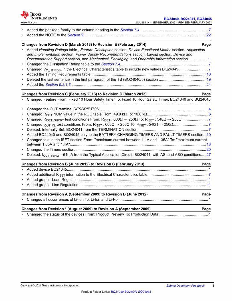
7.6 Timing RequirementsMIN NOM MAX UNIT
INPUT
tDGL(PG_PWR) Deglitch time on exiting sleep. Time measured from VIN: 0V → 5V 1μs rise-time toPG = low, VOUT = 3.6V
45 μs
tDGL(PG_NO-PWR)
Deglitch time on VHYS-INDT power down.Same as entering sleep.
Time measured from VIN: 5V → 3.2V 1μs fall-time toPG = OC, VOUT = 3.6V
29 ms
tDGL(OVP-SET) Input over-voltage blanking time VIN: 5V → 12V 113 μs
tDGL(OVP-REC) Deglitch time exiting OVP Time measured from VIN: 12V → 5V 1μs fall-time toPG = LO
30 μs
ISET SHORT CIRCUIT TEST
tDGL_SHORT Deglitch time transition from ISET short toIOUT disable
Clear fault by disconnecting IN or cycling (high / low)TS/ BAT_EN
1 ms
PRECHARGE – SET BY PRETERM PIN: BQ24040 / BQ24045; Internally Set: BQ24041
tDGL1(LOWV) Deglitch time on pre-charge to fast-chargetransition
70 μs
tDGL2(LOWV) Deglitch time on fast-charge to pre-chargetransition
32 ms
TERMINATION – SET BY PRE-TERM PIN: BQ24040 / BQ24045
tDGL(TERM) Deglitch time, termination detected 29 ms
tTerm-Start Elevated termination threshold initiallyactive for tTerm-Start
1.25 min
RECHARGE OR REFRESH – BQ24040 / BQ24045
tDGL1(RCH) Deglitch time, recharge threshold detected VIN = 5V, VTS = 0.5V, VOUT: 4.25V → 3.5V in 1μs;tDGL(RCH) is time to ISET ramp
29 ms
tDGL2(RCH) Deglitch time, recharge threshold detectedin OUT-Detect Mode
VIN = 5V, VTS = 0.5V, VOUT = 3.5V inserted; tDGL(RCH)is time to ISET ramp
3.6 ms
BATTERY DETECT ROUTINE – BQ24040 / BQ24045 (NOTE: In Hot mode VO(REG) becomes VO_HT(REG))
tDGL(HI/LOWREG)
Regulation time at VREG or VREG-BD 25 ms
BATTERY CHARGING TIMERS AND FAULT TIMERS: BQ24040 and BQ24045 only
tPRECHG Pre-charge safety timer value Restarts when entering Pre-charge; Always enabledwhen in pre-charge.
1700 1940 2250 s
tMAXCH Charge safety timer value Clears fault or resets at UVLO, TS/ BAT_EN disable,OUT Short, exiting LOWV and Refresh
34000 38800 45000 s
BATTERY-PACK NTC MONITOR; TS Terminal: BQ24040 / BQ24045: 10k NTC
tDGL(TTDM) Deglitch exit TTDM between states 57 ms
Deglitch enter TTDM between states 8 μs
tDGL(TS_10C) Deglitch for TS thresholds: 10C. Normal to Cold Operation; VTS: 0.6V → 1V 50 ms
Cold to Normal Operation; VTS: 1V → 0.6V 12 ms
tDGL(TS) Deglitch for TS thresholds: 0/45/60C. Battery charging 30 ms
BQ24040, BQ24041, BQ24045SLUS941H – SEPTEMBER 2009 – REVISED FEBRUARY 2021 www.ti.com
10 Submit Document Feedback Copyright © 2021 Texas Instruments Incorporated
Product Folder Links: BQ24040 BQ24041 BQ24045

7.7 Typical Operational Characteristics (Protection Circuits Waveforms)SETUP: BQ24040 typical applications schematic; VIN = 5V, VBAT = 3.6V (unless otherwise indicated)
528
530
532
534
536
538
540
542
544
546
0 0.2 0.4 0.6 0.8
I - Output Current - AO
Kiset
Kis
et
-W
.15
Low to High Currents(may occur in recharge to fast charge transion)
High to Low Currents(may occur in Voltage Regulation - Taper Current)
Figure 7-1. Kiset for Low and High Currents
4.196
4.198
4.2
4.202
4.204
4.206
4.208
4.21
4.212
4.5 5 5.5 6 6.5
R = 100OUT
Ω
V at 25°CO
V at 85°CO
V - Input Voltage DC - VI
V-
Ou
tpu
t V
olt
ag
e D
C -
VO
UT
V at 0°CO
Figure 7-2. Line Regulation
4.192
4.193
4.194
4.195
4.196
4.197
4.198
4.199
4.2
0 0.2 0.4 0.6 0.8 1
I - Output current - AO
V at 0°Creg
V-
Ou
tpu
t V
olt
ag
e -
VO
UT
V at 25°Creg
V at 85°Creg
Figure 7-3. Load Regulation Over Temperature
I - Current - mALOAD
V-
Vo
ltag
e -
VR
EG
4.34
4.342
4.344
4.346
4.348
4.35
4.352
100 200 300 400 500 600 700 800 9000
V at 85°CREG
V at 0°CREG
V at 25°CREG
V at 125°CREG
Figure 7-4. Load Regulation
V - Input Voltage - VIN
V-
Ou
tpu
t V
olt
ag
e -
VO
UT
5 5.5 6 6.5 74.54.3415
4.3420
4.3425
4.3430
4.3435
4.3440
4.3445
4.3450
V at 0°CREG
V at 25°CREG
V at 85°CREG
Figure 7-5. Line Regulation
361.8
362
362.2
362.4
362.6
362.8
363
363.2
363.4
2.5 3 3.5 4 4.5
V - Output Voltage - VO
I at 85°CO
I at 25°CO
I-
Ou
tpu
t C
urr
en
t -
mA
O
I at 0°CO
Figure 7-6. Current Regulation Over Temperature
www.ti.comBQ24040, BQ24041, BQ24045
SLUS941H – SEPTEMBER 2009 – REVISED FEBRUARY 2021
Copyright © 2021 Texas Instruments Incorporated Submit Document Feedback 11
Product Folder Links: BQ24040 BQ24041 BQ24045

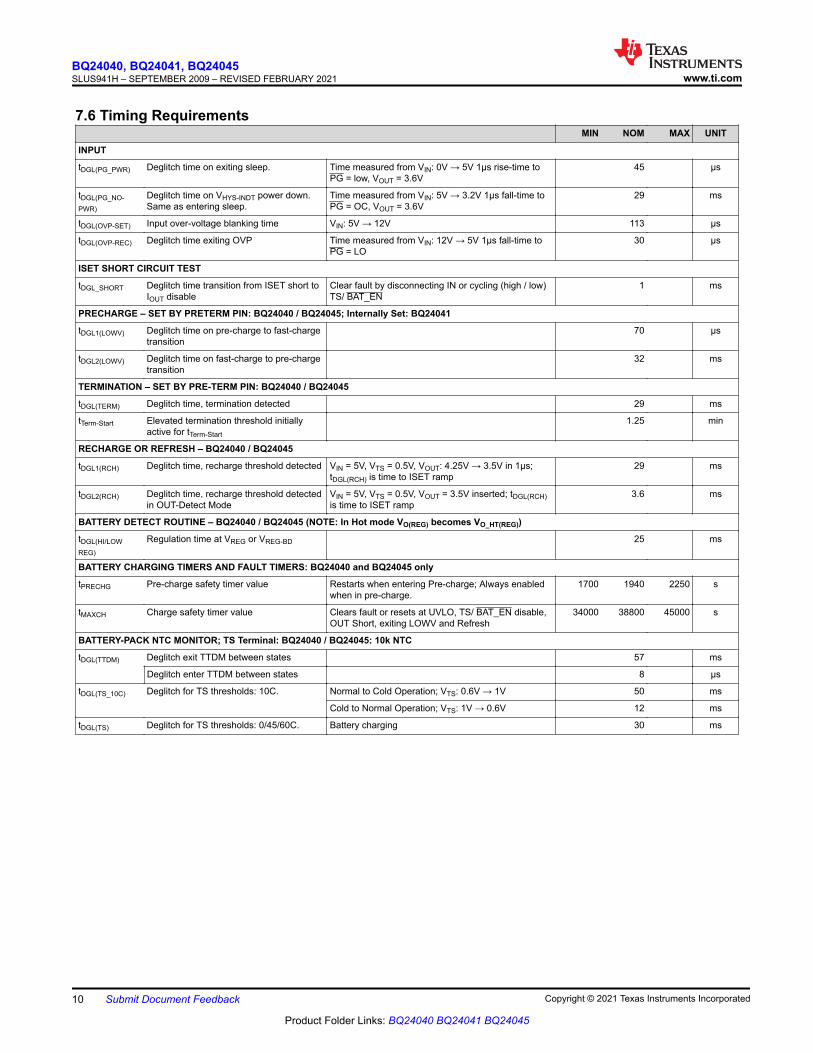
8 Detailed Description8.1 OverviewThe BQ2404x is a highly integrated family of 2×2 single cell Li-Ion and Li-Pol chargers. The charger can be usedto charge a battery, power a system or both. The charger has three phases of charging: Pre-charge to recover afully discharged battery, fast-charge constant current to supply the buck charge safely and voltage regulation tosafely reach full capacity. The charger is very flexible, allowing programming of the fast-charge current and Pre-charge/Termination Current (BQ24040/5 only). This charger is designed to work with a USB connection orAdaptor (DC out). The charger also checks to see if a battery is present.
The charger also comes with a full set of safety features: JEITA Temperature Standard (BQ24040/5 only), Over-Voltage Protection, DPM-IN, Safety Timers, and ISET short protection. All of these features and more aredescribed in detail below.
The charger is designed for a single power path from the input to the output to charge a single cell Li-Ion orLi-Pol battery pack. Upon application of a 5VDC power source the ISET and OUT short checks are performed toassure a proper charge cycle.
If the battery voltage is below the LOWV threshold, the battery is considered discharged and a preconditioningcycle begins. The amount of precharge current can be programmed using the PRE-TERM terminal whichprograms a percent of fast charge current (10 to 100%) as the precharge current. This feature is useful when thesystem load is connected across the battery “stealing” the battery current. The precharge current can be sethigher to account for the system loading while allowing the battery to be properly conditioned. The PRE-TERMterminal is a dual function terminal which sets the precharge current level and the termination threshold level.The termination "current threshold" is always half of the precharge programmed current level.
Once the battery voltage has charged to the VLOWV threshold, fast charge is initiated and the fast chargecurrent is applied. The fast charge constant current is programmed using the ISET terminal. The constantcurrent provides the bulk of the charge. Power dissipation in the IC is greatest in fast charge with a lower batteryvoltage. If the IC reaches 125°C the IC enters thermal requlation, slows the timer clock by half and reduce thecharge current as needed to keep the temperature from rising any further. Figure 8-1 shows the charging profilewith thermal regulation. Typically under normal operating conditions, the IC’s junction temperature is less than125°C and thermal regulation is not entered.
Once the cell has charged to the regulation voltage the voltage loop takes control and holds the battery at theregulation voltage until the current tapers to the termination threshold. The termination can be disabled ifdesired. The CHG terminal is low (LED on) during the first charge cycle only and turns off once the terminationthreshold is reached, regardless if termination, for charge current, is enabled or disabled.
Further details are mentioned in the Operating Modes section.
BQ24040, BQ24041, BQ24045SLUS941H – SEPTEMBER 2009 – REVISED FEBRUARY 2021 www.ti.com
12 Submit Document Feedback Copyright © 2021 Texas Instruments Incorporated
Product Folder Links: BQ24040 BQ24041 BQ24045

8.2 Functional Block Diagram
OUT
Charge
Pump
IN OUT
OUTREGREF
TJ°C
125°CREF
IN
IN
ISET
Charge
Pump
PRE-TERM
75 Am+
CHARGE
CONTROL
OUT
VTERM_EN
ISET2 (LO = ISET, HI = USB500,
FLOAT = USB100)
VCOLD-FLT
VHOT-45 Co
VTTDM
VCE
TS/BAT_EN
5 Am 45 Am
VCLAMP = 1.4V
Cold Temperature
Sink Current
= 45 Am
LO = TTDM MODE
HI=CHIP DISABLE
OUT
CHG
ON:
On During1st Charge Only
OFF:
+Increased from 75 A to 85 A form m
1st
minute of charge.
+_ +
_
+_
+_
+_
+_
+_
+_
+_
+_
+_
Internal Charge
Current Sense
w/ Multiple Outputs
+_
USB Sense
Resistor
USB100/500REF
+_
1.5V
FAST CHARGE
PRE-CHARGE
PG
HI = Suspend CHG
VCOLD-10 Co
VHOT-FLT
+_
+_
HI = Half CHG (JEITA)
HI = 4.06Vreg (JEITA)
VDISABLE
+_
BQ24041This Comparator Only – No TS Features
ASI
ASO
OUT
+
-80 mV Input
Power
Detect+_
IN-DPMREF
0.9V Float
BQ24041
Only
BQ24040 andBQ24045 Only
TS - BQ24040 andBQ24045
BAT_EN - bq24041
+_
Disable
Sink Current
= 20 Am
200kW
BQ24040 and BQ24045 are as shown
BQ24041has no Current Sinks and only 5 A Current Sourcem
X2 Gain (1: 2)Term:Pre-CHGX2
Term Reference
Pre-CHG Reference
I x 1.5 VOUT
540 AW
T CJo
+_
150 Co
REFThermal Shutdown
IN
+_
OVPREF
www.ti.comBQ24040, BQ24041, BQ24045
SLUS941H – SEPTEMBER 2009 – REVISED FEBRUARY 2021
Copyright © 2021 Texas Instruments Incorporated Submit Document Feedback 13
Product Folder Links: BQ24040 BQ24041 BQ24045
8.3 Feature Description
PRE-CHARGECURRENT ANDTERMINATIONTHRESHOLD
FAST-CHARGECURRENT
T(PRECHG)
ChargeComplete
Status,Charger
Off
Pre-Conditioning
Phase
CurrentRegulation
Phase
Voltage Regulation andCharge Termination
Phase
BatteryVoltage,V(OUT)
Battery Current,I(OUT)
DONE
0A
ThermalRegulation
Phase
Temperature, Tj
IO(OUT)
T(THREG)
I(TERM)IO(PRECHG)
VO(REG)
VO(LOWV)
DONET(CHG)
Figure 8-1. Charging Profile With Thermal Regulation
8.3.1 Power-Down or Undervoltage Lockout (UVLO)
The BQ2404x family is in power down mode if the IN terminal voltage is less than UVLO. The part is considered“dead” and all the terminals are high impedance. Once the IN voltage rises above the UVLO threshold the IC willenter Sleep Mode or Active mode depending on the OUT terminal (battery) voltage.
8.3.2 Power-up
The IC is alive after the IN voltage ramps above UVLO (see sleep mode), resets all logic and timers, and startsto perform many of the continuous monitoring routines. Typically the input voltage quickly rises through theUVLO and sleep states where the IC declares power good, starts the qualification charge at 100mA, sets theinput current limit threshold base on the ISET2 terminal, starts the safety timer and enables the CHG terminal.See Figure 8-2.
8.3.3 Sleep Mode
If the IN terminal voltage is between than VOUT+VDT and UVLO, the charge current is disabled, the safety timercounting stops (not reset) and the PG and CHG terminals are high impedance. As the input voltage rises and thecharger exits sleep mode, the PG terminal goes low, the safety timer continues to count, charge is enabled andthe CHG terminal returns to its previous state. See Figure 8-3.
8.3.4 New Charge Cycle
A new charge cycle is started when any of these events occur:• A valid power source is applied;• The chip is enabled/disabled using TS pin or BAT_EN;• Exit of termination/Timer Disable Mode (TTDM);• Detection of batter insertion;• OUT voltage drops below the VRCH threshold.
The CHG signal is active only during the first charge cycle. Exiting TTDM or the OUT voltage falling below VRCHwill not activate the CHG signal if it is already in the open-drain (off) state.
BQ24040, BQ24041, BQ24045SLUS941H – SEPTEMBER 2009 – REVISED FEBRUARY 2021 www.ti.com
14 Submit Document Feedback Copyright © 2021 Texas Instruments Incorporated
Product Folder Links: BQ24040 BQ24041 BQ24045

LDO
VSS
1.8V
0V
LDOHYS
0°C
0°CHYS
10°C
10°CHYS
45°C
45°CHYS
60°C
60°CHYS
EN
DISHYS
tDGL(TS)
tDGL(TS)
tDGL(TS)
tDGL(TS)
tDGL(TS_IOC)
Rising
tDGL(TS_IOC)
Falling
tDGL(TS)
tDGL(TS)
tDGL(TTDM)
Exit
tDGL(TTDM)
Enter
t < tDGL(TTDM)
Exit
t < tDGL(IS)
NormalOperation
LDOMode
NormalOperation
ColdOperation
ColdFault
LDOMode
ColdFault
NormalOperation
tDGL(TS)
tDGL(TTDM)
Enter
DisabledCold
OperationHOTFault
4.06 VHOT
OperationNormal
Operation
4.06 VHOT
OperationDisabled
tDGL(TS1_IOC)
Cold to Normal
Drawing Not to Scale
Dots Show Threshold Trip Pointsfllowed by a deglitch time beforetransitioning into a new mode.
t
Figure 8-2. TS Battery Temperature Bias Threshold and Deglitch Timers
www.ti.comBQ24040, BQ24041, BQ24045
SLUS941H – SEPTEMBER 2009 – REVISED FEBRUARY 2021
Copyright © 2021 Texas Instruments Incorporated Submit Document Feedback 15
Product Folder Links: BQ24040 BQ24041 BQ24045

Apply Input
Power
Set Input Current Limit to 100 mA
and Start Charge
Perform ISET & OUT short tests
Remember ISET2 State
Set charge current
based on ISET2 truth
table.
Return to
Charge
Is power good?
VBAT+VDT < VIN < VOVP
& VUVLO < VIN
No
Yes
Is chip enabled?
VTS > VEN
No
Yes
Turn on PG FET
PG pin LOW
Figure 8-3. BQ2404x Power-Up Flow Diagram
8.3.5 Overvoltage-Protection (OVP) – Continuously Monitored
If the input source applies an overvoltage, the pass FET, if previously on, turns off after a deglitch, tBLK(OVP). Thetimer ends and the CHG and PG terminal goes to a high impedance state. Once the overvoltage returns to anormal voltage, the PG terminal goes low, timer continues, charge continues and the CHG terminal goes lowafter a 25ms deglitch. PG terminal is optional on some packages
8.3.6 Power Good Indication ( PG)
After application of a 5V source, the input voltage rises above the UVLO and sleep thresholds (VIN>VBAT+VDT),but is less than OVP (VIN<VOVP,), then the PG FET turns on and provides a low impedance path to ground. SeeFigure 9-6, Figure 9-7, and Figure 9-19.
BQ24040, BQ24041, BQ24045SLUS941H – SEPTEMBER 2009 – REVISED FEBRUARY 2021 www.ti.com
16 Submit Document Feedback Copyright © 2021 Texas Instruments Incorporated
Product Folder Links: BQ24040 BQ24041 BQ24045
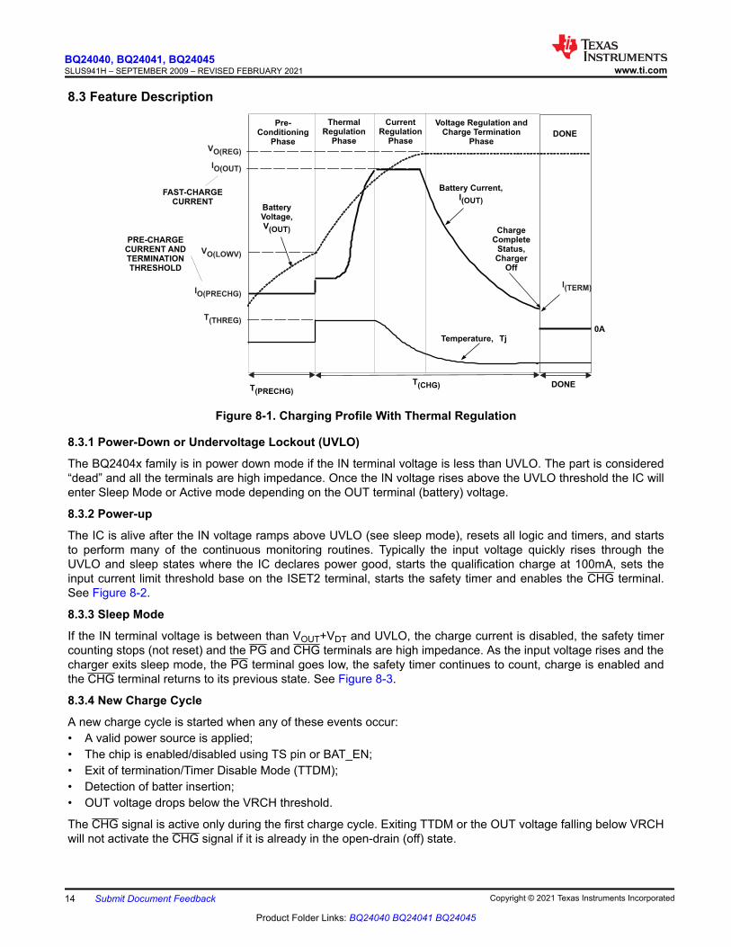
8.3.7 CHG Terminal Indication
The charge terminal has an internal open drain FET which is on (pulls down to VSS) during the first charge only(independent of TTDM) and is turned off once the battery reaches voltage regulation and the charge currenttapers to the termination threshold set by the PRE-TERM resistor. The BQ24041 does not terminate charge,however, the CHG terminal will turn off once the battery current reaches 10% of the programmed charge current.
The charge terminal is high impedance in sleep mode and OVP (if PG is high impedance) and return to itsprevious state once the condition is removed.
Cycling input power, pulling the TS terminal low and releasing or entering pre-charge mode causes the CHGterminal to go reset (go low if power is good and a discharged battery is attached) and is considered the start ofa first charge.
8.4 Device Functional Modes8.4.1 CHG and PG LED Pull-up Source
For host monitoring, a pullup resistor is used between the STATUS terminal and the VCC of the host and for avisual indication a resistor in series with an LED is connected between the STATUS terminal and a powersource. If the CHG or PG source is capable of exceeding 7V, a 6.2V Zener should be used to clamp the voltage.If the source is the OUT terminal, note that as the battery changes voltage, and the brightness of the LEDs vary.
Table 8-1.CHARGING STATE CHG FET/LED
First charge after VIN applied ON
Refresh charge
OFFOVP
SLEEP
TEMP FAULT ON for 1st Charge
Table 8-2.VIN POWER GOOD STATE PG FET/LED
UVLO
OFFSLEEP mode
OVP mode
Normal input (VOUT + VDT < VIN <VOUP) ON
PG is independent of chip disable
8.4.2 Auto Start-up (BQ24041)
The auto start-up feature is an OR gate with two inputs; an internal power good signal (logic 1 when VIN>VBAT +VIN-DT) and an external input from ASI terminal (internal 100kΩ pull-down). The ASO terminal outputs a signalthat can be used as a system boot signal. The OR gate is powered by the OUT terminal and the OUT terminalmust be powered by an external source (battery or P/S) or via the IN terminal for the ASO terminal to deliver alogic High. The ASI and/or the internal power good signal have to be logic high for the ASO to be logic high. TheASI/ASO, OUT and PG signals are used in production testing to test the system without a battery.
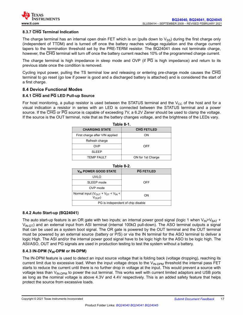
8.4.3 IN-DPM (VIN-DPM or IN-DPM)
The IN-DPM feature is used to detect an input source voltage that is folding back (voltage dropping), reaching itscurrent limit due to excessive load. When the input voltage drops to the VIN-DPM threshold the internal pass FETstarts to reduce the current until there is no further drop in voltage at the input. This would prevent a source withvoltage less than VIN-DPM to power the out terminal. This works well with current limited adaptors and USB portsas long as the nominal voltage is above 4.3V and 4.4V respectively. This is an added safety feature that helpsprotect the source from excessive loads.
www.ti.comBQ24040, BQ24041, BQ24045
SLUS941H – SEPTEMBER 2009 – REVISED FEBRUARY 2021
Copyright © 2021 Texas Instruments Incorporated Submit Document Feedback 17
Product Folder Links: BQ24040 BQ24041 BQ24045

8.4.4 OUT
The Charger’s OUT terminal provides current to the battery and to the system, if present. This IC can be used tocharge the battery plus power the system, charge just the battery or just power the system (TTDM) assuming theloads do not exceed the available current. The OUT terminal is a current limited source and is inherentlyprotected against shorts. If the system load ever exceeds the output programmed current threshold, the outputwill be discharged unless there is sufficient capacitance or a charged battery present to supplement theexcessive load.
8.4.5 ISET
An external resistor is used to Program the Output Current (50 to 1000mA) and can be used as a currentmonitor.
RISET = KISET / IOUT (1)
where
• IOUT is the desired fast charge current;• KISET is a gain factor found in the electrical specification
For greater accuracy at lower currents, part of the sense FET is disabled to give better resolution. Figure 7-1shows the transition from low current to higher current. Going from higher currents to low currents, there ishysteresis and the transition occurs around 0.15A.
The ISET resistor is short protected and will detect a resistance lower than ≉340Ω. The detection requires atleast 80mA of output current. If a “short” is detected, then the IC will latch off and can only be reset by cycling thepower. The OUT current is internally clamped to a maximum current between 1.05A and 1.4A and isindependent of the ISET short detection circuitry, as shown in Figure 8-5. Also, see Figure 9-14 and Figure 9-15.
0
0.5
1
1.5
2
2.5
3
3.5
4
4.5
0.6 1.8
V - Voltage - VTS
No
rmalized
OU
T C
urr
en
t an
d V
- V
RE
G 60 C to 45 CHOT TEMP
4.06VRegulation
o o
IOUT
VOUT
0 0.2 0.4 0.8 1 1.2 1.4 1.6
For < 45 C, 4.2V Regulationo
H
ot F
ault
No OperationDuring Cold
Fault
ColdFault
IC D
isable
0 Co
< 48 Co
60 Co
10 Co
100% of ProgrammedCurrent
50%
Term
ination
Dis
able
Figure 8-4. Operation Over TS Bias Voltage(BQ24040)
0
0.2
0.4
0.6
0.8
1
1.2
1.4
1.6
1.8
100 1000 10000
I -SET W
I-
Ou
tpu
t C
urr
en
t -
AO
I Internal Clamp RangeOUT
I Short
FaultRange
SET
Non RestrictedOperating Area
I ProgrammedOUT
min
max
IC
lam
p m
in -
max
OU
T
IF
ault m
in -
max
OU
T
Figure 8-5. Programmed/Clamped Out Current(BQ24040)
8.4.6 PRE_TERM – Pre-Charge and Termination Programmable Threshold, BQ24040/5
Pre-Term is used to program both the pre-charge current and the termination current threshold. The pre-chargecurrent level is a factor of two higher than the termination current level. The termination can be set between 5and 50% of the programmed output current level set by ISET. If left floating the termination and pre-charge areset internally at 10/20% respectively. The pre-charge-to-fast-charge, Vlowv threshold is set to 2.5V.
RPRE-TERM = %Term × KTERM = %Pre-CHG × KPRE-CHG (2)
where
BQ24040, BQ24041, BQ24045SLUS941H – SEPTEMBER 2009 – REVISED FEBRUARY 2021 www.ti.com
18 Submit Document Feedback Copyright © 2021 Texas Instruments Incorporated
Product Folder Links: BQ24040 BQ24041 BQ24045

• %Term is the percent of fast charge current where termination occurs;• %Pre-CHG is the percent of fast charge current that is desired during precharge;• KTERM and KPRE-CHG are gain factors found in the electrical specifications.
8.4.7 ISET2
ISET2 is a 3-state input and programs the Input Current Limit/Regulation Threshold. A low will program aregulated fast charge current via the ISET resistor and is the maximum allowed input/output current for anyISET2 setting, Float will program a 100mA Current limit and High will program a 500mA Current limit.
Below are two configurations for driving the 3-state ISET2 terminal:
DriveLogic
VCC
ToISET2
R1
R2
To ISET2
VCC
Q1
Q2
DriveLogic
R1 Dividerset to 0.9 VWhich is theFloat VoltageOR
Figure 8-6. 3-State ISET2 Terminal Circuits
8.4.8 TS (BQ24040/5)
The TS function for the BQ24040/5 is designed to follow the new JEITA temperature standard for Li-Ion and Li-Pol batteries. There are now four thresholds, 60°C, 45°C, 10°C, and 0°C. Normal operation occurs between10°C and 45°C. If between 0°C and 10°C the charge current level is cut in half and if between 45°C and 60°Cthe regulation voltage is reduced to 4.1Vmax, see Figure 8-4.
The TS feature is implemented using an internal 50μA current source to bias the thermistor (designed for usewith a 10k NTC β = 3370 (SEMITEC 103AT-2 or Mitsubishi TH05-3H103F) connected from the TS terminal toVSS. If this feature is not needed, a fixed 10kΩ can be placed between TS and VSS to allow normal operation.This may be done if the host is monitoring the thermistor and then the host would determine when to pull the TSterminal low to disable charge.
The TS terminal has two additional features, when the TS terminal is pulled low or floated/driven high. A lowdisables charge (similar to a high on the BAT_EN feature) and a high puts the charger in TTDM.
Above 60°C or below 0°C the charge is disabled. Once the thermistor reaches ≉–10°C the TS current folds backto keep a cold thermistor (between –10°C and –50°C) from placing the IC in the TTDM mode. If the TS terminalis pulled low into disable mode, the current is reduce to ≉30μA, see Figure 8-2. Since the ITS curent is fixedalong with the temperature thresholds, it is not possible to use thermistor values other than the 10k NTC (at25°C).
www.ti.comBQ24040, BQ24041, BQ24045
SLUS941H – SEPTEMBER 2009 – REVISED FEBRUARY 2021
Copyright © 2021 Texas Instruments Incorporated Submit Document Feedback 19
Product Folder Links: BQ24040 BQ24041 BQ24045

8.4.9 Termination and Timer Disable Mode (TTDM) - TS Terminal High
The battery charger is in TTDM when the TS terminal goes high from removing the thermistor (removing batterypack/floating the TS terminal) or by pulling the TS terminal up to the TTDM threshold.
When entering TTDM, the 10 hour safety timer is held in reset and termination is disabled. A battery detectroutine is run to see if the battery was removed or not. If the battery was removed then the CHG terminal will goto its high impedance state if not already there. If a battery is detected the CHG terminal does not change statesuntil the current tapers to the termination threshold, where the CHG terminal goes to its high impedance state ifnot already there (the regulated output will remain on).
The charging profile does not change (still has pre-charge, fast-charge constant current and constant voltagemodes). This implies the battery is still charged safely and the current is allowed to taper to zero.
When coming out of TTDM, the battery detect routine is run and if a battery is detected, then a new charge cyclebegins and the CHG LED turns on.
If TTDM is not desired upon removing the battery with the thermistor, one can add a 237k resistor between TSand VSS to disable TTDM. This keeps the current source from driving the TS terminal into TTDM. This creates≉0.1°C error at hot and a ≉3°C error at cold.
8.4.10 Timers, BQ24040 and BQ24045 only
The pre-charge timer is set to 30 minutes. The pre-charge current, can be programmed to off-set any systemload, making sure that the 30 minutes is adequate. The BQ24041 does not have a safety timer.
The fast charge timer is fixed at 10 hours and can be increased real time by going into thermal regulation, IN-DPM or if in USB current limit. The timer clock slows by a factor of 2, resulting in a clock than counts half as fastwhen in these modes. If either the 30 minute or ten hour timer times out, the charging is terminated and the CHGterminal goes high impedance if not already in that state. The timer is reset by disabling the IC, cycling power orgoing into and out of TTDM.
8.4.11 Termination
Once the OUT terminal goes above VRCH, (reaches voltage regulation) and the current tapers down to thetermination threshold, the CHG terminal goes high impedance and a battery detect route is run to determine ifthe battery was removed or the battery is full. If the battery is present, the charge current will terminate. If thebattery was removed along with the thermistor, then the TS terminal is driven high and the charge enters TTDM.If the battery was removed and the TS terminal is held in the active region, then the battery detect routine willcontinue until a battery is inserted.
8.4.12 Battery Detect Routine
The battery detect routine should check for a missing battery while keeping the OUT terminal at a useablevoltage. Whenever the battery is missing the CHG terminal should be high impedance.
The battery detect routine is run when entering and exiting TTDM to verify if battery is present, or run all the timeif battery is missing and not in TTDM. On power-up, if battery voltage is greater than VRCH threshold, a batterydetect routine is run to determine if a battery is present.
The battery detect routine is disabled while the IC is in TTDM, or has a TS fault. See Figure 8-7 for the BatteryDetect Flow Diagram.
8.4.13 Refresh Threshold
After termination, if the OUT terminal voltage drops to VRCH (100mV below regulation) then a new charge isinitiated, but the CHG terminal remains at a high impedance (off).
8.4.14 Starting a Charge on a Full Battery
The termination threshold is raised by ≉14%, for the first minute of a charge cycle so if a full battery is removedand reinserted or a new charge cycle is initiated, that the new charge terminates (less than 1 minute). Batteriesthat have relaxed many hours may take several minutes to taper to the termination threshold and terminatecharge.
BQ24040, BQ24041, BQ24045SLUS941H – SEPTEMBER 2009 – REVISED FEBRUARY 2021 www.ti.com
20 Submit Document Feedback Copyright © 2021 Texas Instruments Incorporated
Product Folder Links: BQ24040 BQ24041 BQ24045

Start
BATT_DETECT
Start 25ms timer
Timer Expired?
Is VOUT<VREG-100mV?
Battery Present
Turn off Sink Current
Return to flow
Set OUT REG
to VREG-400mV
Enable sink current
Reset & Start 25ms timer
No
Yes
Timer Expired?No
Yes
Is VOUT>VREG-300mV?
Battery Present
Turn off Sink Current
Return to flow
Yes
No
Yes
No
Battery Absent
Don’t Signal Charge
Turn off Sink Current
Return to Flow
Figure 8-7. Battery Detect Routine (BQ24040)
www.ti.comBQ24040, BQ24041, BQ24045
SLUS941H – SEPTEMBER 2009 – REVISED FEBRUARY 2021
Copyright © 2021 Texas Instruments Incorporated Submit Document Feedback 21
Product Folder Links: BQ24040 BQ24041 BQ24045

9 Application and ImplementationNote
Information in the following applications sections is not part of the TI component specification, and TIdoes not warrant its accuracy or completeness. TI’s customers are responsible for determiningsuitability of components for their purposes. Customers should validate and test their designimplementation to confirm system functionality.
9.1 Application InformationThe BQ2404x series of devices are highly integrated Li-Ion and Li-Pol linear chargers devices targeted at space-limited portable applications. The devices operate from either a USB port or AC adapter. The high input voltagerange with input overvoltage protection supports low-cost unregulated adapters. These devices have a singlepower output that charges the battery. A system load can be placed in parallel with the battery as long as theaverage system load does not keep the battery from charging fully during the 10 hour safety timer.
9.2 Typical Applications9.2.1 Typical Application: BQ24040 and BQ24045
IOUT_FAST_CHG = 540mA; IOUT_PRE_CHG = 108mA; IOUT_TERM = 54mA
Battery Pack
VBUS
GND
D+
D-
USB Port
DC+
GND
Adaptor
VDD
D-
D+
GND
Host
System Load
OR
ISET/100/500 mA
1
2
3
4
5
10
9
8
7
6
IN
ISET
VSS
PRETERM
PG NC
ISET2
CHG
TS
OUT
BQ24040 and BQ24045
1 Fm1 Fm1kW
1.5kW
1.5kW
2kW
+
TTDM/BAT_EN
+
Figure 9-1. Typical Application Circuit: BQ24040 and BQ24045
9.2.1.1 Design Requirements
• Supply voltage = 5 V• Fast charge current: IOUT-FC = 540 mA; ISET-terminal 2• Termination Current Threshold: %IOUT-FC = 10% of Fast Charge or about 54mA• Pre-Charge Current by default is twice the termination Current or about 108mA• TS – Battery Temperature Sense = 10k NTC (103AT)
BQ24040, BQ24041, BQ24045SLUS941H – SEPTEMBER 2009 – REVISED FEBRUARY 2021 www.ti.com
22 Submit Document Feedback Copyright © 2021 Texas Instruments Incorporated
Product Folder Links: BQ24040 BQ24041 BQ24045

9.2.1.2 Detailed Design Procedure9.2.1.2.1 Calculations
For additional information on calculations, refer to BQ24040 Application Report.
9.2.1.2.1.1 Program the Fast Charge Current, ISET:
RISET = [K(ISET) / I(OUT)] (3)
From Section 7.5:• K(SET) = 540AΩ• RISET = [540AΩ/0.54A] = 1.0 kΩ
Selecting the closest standard value, use a 1.0 kΩ resistor between ISET (terminal 16) and VSS.
9.2.1.2.1.2 Program the Termination Current Threshold, ITERM:
RPRE-TERM = K(TERM) × %IOUT-FC (4)
RPRE-TERM = 200Ω/% × 10% = 2kΩ (5)
Selecting the closest standard value, use a 2 kΩ resistor between ITERM (terminal 15) and VSS.
One can arrive at the same value by using 20% for a pre-charge value (factor of 2 difference).
RPRE-TERM = K(PRE-CHG) × %IOUT-FC (6)
RPRE-TERM = 100Ω/% × 20%= 2kΩ (7)
9.2.1.2.1.3 TS Function (BQ24040)
Use a 10k NTC thermistor in the battery pack (103AT).
To Disable the temp sense function, use a fixed 10k resistor between the TS (terminal 1) and VSS.
9.2.1.2.1.4 CHG and PG
LED Status: connect a 1.5k resistor in series with a LED between the OUT terminal and the CHG terminal.Connect a 1.5k resistor in series with a LED between the OUT terminal and the and PG terminal.
Processor Monitoring: Connect a pull-up resistor between the processor’s power rail and the CHG terminal.Connect a pull-up resistor between the processor’s power rail and the PG terminal.
9.2.1.2.2 Selecting In and Out Terminal Capacitors
In most applications, all that is needed is a high-frequency decoupling capacitor (ceramic) on the power terminal,input and output terminals. Using the values shown on the application diagram, is recommended. Afterevaluation of these voltage signals with real system operational conditions, one can determine if capacitancevalues can be adjusted toward the minimum recommended values (DC load application) or higher values for fasthigh amplitude pulsed load applications. Note if designed for high input voltage sources (bad adaptors or wrongadaptors), the capacitor needs to be rated appropriately. Ceramic capacitors are tested to 2x their rated valuesso a 16V capacitor may be adequate for a 30V transient (verify tested rating with capacitor manufacturer).
www.ti.comBQ24040, BQ24041, BQ24045
SLUS941H – SEPTEMBER 2009 – REVISED FEBRUARY 2021
Copyright © 2021 Texas Instruments Incorporated Submit Document Feedback 23
Product Folder Links: BQ24040 BQ24041 BQ24045

9.2.1.3 Application Curves
SETUP: BQ24040 typical applications schematic; VIN = 5V, VBAT = 3.6V (unless otherwise indicated)
Vaso
Vpg
t - time - 10ms/div
5V/div
5V/div
5V/div
5V/div
Vin
Vout
Figure 9-2. Power-up Timing
Vpg
Vaso
t - time - 10ms/div
5V/div
5V/div
5V/div
5V/div
Vin
Vout
Figure 9-3. Power-up Timing – No Battery or Load
Vaso
Vpg
t - time - 20ms/div
5V/div
5V/div
5V/div
5V/div
Vasi
Vout
Figure 9-4. – ASI and OUT Power-up Timing – NoInput
Vpg
t - time - 50ms/div
5V/div
5V/div5V/div
5V/div
Vasi
Vas
Vout
Figure 9-5. ASI and delayed OUT Power-up Timing– No Input
Vin
Viset
Vchg
Vpg
t - time - 20ms/div
2V/div
2V/div
5V/div
2V/div
Figure 9-6. OVP 8V Adaptor - Hot Plug
Vin
Viset
Vchg
Vpg
t - time - 100ms/div
2V/div
2V/div
2V/div
5V/div
Figure 9-7. OVP from Normal Power-up Operation– VIN 0V → 5V → 8V →5V
BQ24040, BQ24041, BQ24045SLUS941H – SEPTEMBER 2009 – REVISED FEBRUARY 2021 www.ti.com
24 Submit Document Feedback Copyright © 2021 Texas Instruments Incorporated
Product Folder Links: BQ24040 BQ24041 BQ24045

Vts
Viset
Vchg
Vpg
t - time - 50ms/div
2V/div
2V/div
2V/div
500mV/div
10kΩ resistor from TS to GND. 10kΩ isshorted to disable the IC
.Figure 9-8. TS Enable and Disable
Vin
Vchg
Vpg
Vout
Battery Detect Mode
t - time - 20ms/div
2V/div
5V/div
5V/div
2V/div
Figure 9-9. Hot Plug Source w/No Battery – BatteryDetection
Vin
Viset
Vts
Vout
t - time - 5ms/div
2V/div
2V/div
1V/div
500mV/div
Figure 9-10. Battery Removal – GND Removed 1st,42 Ω Load
Viset
Vchg
Vts
Vout 1 Battery Detect Cycle
Entered TTDM
t - time - 10ms/div
5V/div
1V/div
1V/div
1V/div
Figure 9-11. Battery Removal with OUT and TSDisconnect 1st, With 100 Ω Load
Viset
Vchg
V_0.1 _OUTW
Vout
Battery Declared Absent
t - time - 20ms/div
100mV/div
1V/div
1V/div
5V/div
Continuous battery detection when not in TTDM
Figure 9-12. Battery Removal with fixed TS = 0.5V
Viset
Vchg
Vout
V_0.1 _OUTW
BatteryThresholdReached
t - time - 500ms/div
1V/div
5V/div
1V/div
100mV/div
CH4: IOUT (1A/Div)Battery voltage swept from 0V to 4.25V to 3.9V.
Figure 9-13. Battery Charge Profile
www.ti.comBQ24040, BQ24041, BQ24045
SLUS941H – SEPTEMBER 2009 – REVISED FEBRUARY 2021
Copyright © 2021 Texas Instruments Incorporated Submit Document Feedback 25
Product Folder Links: BQ24040 BQ24041 BQ24045

Viset
Vchg
Vout
V_0.1 _OUTW
I Clamped CurrentOUT
I Short Detected
and Latched OffSET
t - time - 200 s/divm
1V/div
2V/div
500mV/div
100mV/div
CH4: IOUT (1A/Div)
Figure 9-14. ISET Shorted During NormalOperation
Vin
Viset
Vchg
V_0.1 _OUTW
Short Detected in 100mAmode and Latched Off
t - time - 5ms/div
2V/div
2V/div
500mV/div
20mV/div
CH4: IOUT (0.2A/Div)
Figure 9-15. ISET Shorted Prior to USB Power-up
Vin
Viset
Vchg
V_0.1 _OUTW
t - time - 1ms/div
2V/div
2V/div
20mV/div
500mV/div
CH4: IOUT (0.2A/Div)
Figure 9-16. DPM – Adaptor Current Limits – VinRegulated
Vin
Viset
Vchg
V_0.1 _OUTW
t - time - 500 s/divm
2V/div
2V/div
500mV/div
20mV/div
Figure 9-17. DPM – USB Current Limits – VinRegulated to 4.4V
Viset
VoutVin
V_0.1 _OUTW
ExitsThermal
Regulation
EntersThermalRegulation
t - time - 1s/div
2V/div
1V/div
1V/div
50mV/div
The IC temperature rises to 125°C and enters thermalregulation. Charge current is reduced to regulate the IC at125°C. VIN is reduced, the IC temperature drops, the chargecurrent returns to the programmed value
.Figure 9-18. Thermal Reg. – Vin increases PWR/
Iout Reduced
Vin
Viset
Vchg
Vpg
t - time - 20ms/div
5V/div
5V/div
1V/div
1V/div
VIN swept from 5V to 3.9V to 5V VBAT = 4V
Figure 9-19. Entering and Exiting Sleep mode
BQ24040, BQ24041, BQ24045SLUS941H – SEPTEMBER 2009 – REVISED FEBRUARY 2021 www.ti.com
26 Submit Document Feedback Copyright © 2021 Texas Instruments Incorporated
Product Folder Links: BQ24040 BQ24041 BQ24045

9.2.2 Typical Application Circuit: BQ24041, with ASI and ASO
IOUT_FAST_CHG = 540mA; IOUT_PRE_CHG = 108mA
Battery Pack
VBUS
GND
D+
D-
USB Port
DC+
GND
Adaptor
Power Supply
EN
VDDD-
D+
GND
ISET/100/500 mA
Host
System Load
Auto-BootingOR
1
2
3
4
5
10
9
8
7
6
IN
ISET
VSS
ASI
PG ASO
ISET2
CHG
BAT_EN
OUT
BQ24041
1 Fm 1 Fm
1kW
1.5kW
1.5kW
+
TTDM/BAT_EN
+
Figure 9-20. Typical Application Circuit: BQ24041, with ASI and ASO
9.2.2.1 Design Requirements
See Section 9.2.1 for design requirements.
9.2.2.2 Detailed Design Procedure
See Section 9.2.1 for detailed design procedures.
www.ti.comBQ24040, BQ24041, BQ24045
SLUS941H – SEPTEMBER 2009 – REVISED FEBRUARY 2021
Copyright © 2021 Texas Instruments Incorporated Submit Document Feedback 27
Product Folder Links: BQ24040 BQ24041 BQ24045

9.2.2.3 Application Curves
SETUP: BQ24041 typical applications schematic; VIN = 5V, VBAT = 3.6V (unless otherwise indicated)
Vaso
Vpg
t - time - 10ms/div
5V/div
5V/div
5V/div
5V/div
Vin
Vout
Figure 9-21. Power-up Timing, BQ24041
Vpg
Vaso
t - time - 10ms/div
5V/div
5V/div
5V/div
5V/div
Vin
Vout
Figure 9-22. Power-up Timing – No Battery orLoad, BQ24041
Vaso
Vpg
t - time - 20ms/div
5V/div
5V/div
5V/div
5V/div
Vasi
Vout
Figure 9-23. – ASI and OUT Power-up Timing – NoInput, BQ24041
Vpg
t - time - 50ms/div
5V/div
5V/div5V/div
5V/div
Vasi
Vas
Vout
Figure 9-24. ASI and Delayed OUT Power-upTiming – No Input, BQ24041
BQ24040, BQ24041, BQ24045SLUS941H – SEPTEMBER 2009 – REVISED FEBRUARY 2021 www.ti.com
28 Submit Document Feedback Copyright © 2021 Texas Instruments Incorporated
Product Folder Links: BQ24040 BQ24041 BQ24045

10 Power Supply RecommendationsThe devices are designed to operate from an input voltage supply range between 3.5 V and 28 V and currentcapability of at least the maximum designed charge current. This input supply should be well regulated. If locatedmore than a few inches from the BQ24040x IN and GND terminals, a larger capacitor is recommended.
www.ti.comBQ24040, BQ24041, BQ24045
SLUS941H – SEPTEMBER 2009 – REVISED FEBRUARY 2021
Copyright © 2021 Texas Instruments Incorporated Submit Document Feedback 29
Product Folder Links: BQ24040 BQ24041 BQ24045

11 Layout11.1 Layout GuidelinesTo obtain optimal performance, the decoupling capacitor from IN to GND (thermal pad) and the output filtercapacitors from OUT to GND (thermal pad) should be placed as close as possible to the BQ2405x, with shorttrace runs to both IN, OUT, and GND (thermal pad).
• All low-current GND connections should be kept separate from the high-current charge or discharge pathsfrom the battery. Use a single-point ground technique incorporating both the small signal ground path and thepower ground path.
• The high current charge paths into IN terminal and from the OUT terminal must be sized appropriately for themaximum charge current in order to avoid voltage drops in these traces
• The BQ2404x family is packaged in a thermally enhanced MLP package. The package includes a thermalpad to provide an effective thermal contact between the IC and the printed circuit board (PCB); this thermalpad is also the main ground connection for the device. Connect the thermal pad to the PCB groundconnection. It is best to use multiple 10mil vias in the power pad of the IC and close enough to conduct theheat to the bottom ground plane. The bottom ground plane should avoid traces that “cut off” the thermal path.The thinner the PCB the less temperature rise. The EVM PCB has a thickness of 0.031 inches and uses 2 oz.(2.8mil thick) copper on top and bottom, and is a good example of optimal thermal performance.
11.2 Layout Example
Figure 11-1. Board Layout
BQ24040, BQ24041, BQ24045SLUS941H – SEPTEMBER 2009 – REVISED FEBRUARY 2021 www.ti.com
30 Submit Document Feedback Copyright © 2021 Texas Instruments Incorporated
Product Folder Links: BQ24040 BQ24041 BQ24045

11.3 Thermal ConsiderationsThe BQ2404x family is packaged in a thermally enhanced MLP package. The package includes a thermal pad toprovide an effective thermal contact between the IC and the printed circuit board (PCB). The power pad shouldbe directly connected to the VSS terminal. Full PCB design guidelines for this package are provided in theapplication note entitled: QFN/SON PCB Attachment Application Report. The most common measure ofpackage thermal performance is thermal impedance (RθJA ) measured (or modeled) from the chip junction to theair surrounding the package surface (ambient). The mathematical expression for RθJA is:
RθJA = (TJ – T) / P (8)
where
• TJ = Chip junction temperature• T = Ambient temperature• P = Device power dissipation
Factors that can influence the measurement and calculation of RθJA include:
1. Whether or not the device is board mounted2. Trace size, composition, thickness, and geometry3. Orientation of the device (horizontal or vertical)4. Volume of the ambient air surrounding the device under test and airflow5. Whether other surfaces are in close proximity to the device being tested
Due to the charge profile of Li-Ion and Li-Pol batteries the maximum power dissipation is typically seen at thebeginning of the charge cycle when the battery voltage is at its lowest. Typically after fast charge begins the packvoltage increases to ≉3.4V within the first 2 minutes. The thermal time constant of the assembly typically takes afew minutes to heat up so when doing maximum power dissipation calculations, 3.4V is a good minimum voltageto use. This is verified, with the system and a fully discharged battery, by plotting temperature on the bottom ofthe PCB under the IC (pad should have multiple vias), the charge current and the battery voltage as a function oftime. The fast charge current will start to taper off if the part goes into thermal regulation.
The device power dissipation, P, is a function of the charge rate and the voltage drop across the internalPowerFET. It can be calculated from the following equation when a battery pack is being charged:
P = [V(IN) – V(OUT)] × I(OUT) + [V(OUT) – V(BAT)] × I(BAT) (9)
The thermal loop feature reduces the charge current to limit excessive IC junction temperature. It isrecommended that the design not run in thermal regulation for typical operating conditions (nominal input voltageand nominal ambient temperatures) and use the feature for non typical situations such as hot environments orhigher than normal input source voltage. With that said, the IC will still perform as described, if the thermal loopis always active.
11.3.1 Leakage Current Effects on Battery Capacity
To determine how fast a leakage current on the battery will discharge the battery is an easy calculation. The timefrom full to discharge can be calculated by dividing the Amp-Hour Capacity of the battery by the leakage current.For a 0.75AHr battery and a 10μA leakage current (750 mAHr / 0.010 mA = 75000 hours), it would take 75khours or 8.8 years to discharge. In reality the self discharge of the cell would be much faster so the 10μAleakage would be considered negligible.
www.ti.comBQ24040, BQ24041, BQ24045
SLUS941H – SEPTEMBER 2009 – REVISED FEBRUARY 2021
Copyright © 2021 Texas Instruments Incorporated Submit Document Feedback 31
Product Folder Links: BQ24040 BQ24041 BQ24045

12 Device and Documentation Support12.1 Device Support
12.1.1 Third-Party Products Disclaimer
TI'S PUBLICATION OF INFORMATION REGARDING THIRD-PARTY PRODUCTS OR SERVICES DOES NOTCONSTITUTE AN ENDORSEMENT REGARDING THE SUITABILITY OF SUCH PRODUCTS OR SERVICESOR A WARRANTY, REPRESENTATION OR ENDORSEMENT OF SUCH PRODUCTS OR SERVICES, EITHERALONE OR IN COMBINATION WITH ANY TI PRODUCT OR SERVICE.
12.2 Documentation Support
12.2.1 Related Documentation
For related documentation see the following:• BQ24040 Pin FMA Application Report• BQ2404x FIT Rate Application Report• BQ24040 Application Report• QFN/SON PCB Attachment Application Report
12.3 Receiving Notification of Documentation UpdatesTo receive notification of documentation updates, navigate to the device product folder on ti.com. Click onSubscribe to updates to register and receive a weekly digest of any product information that has changed. Forchange details, review the revision history included in any revised document.
12.4 Support ResourcesTI E2E™ support forums are an engineer's go-to source for fast, verified answers and design help — straightfrom the experts. Search existing answers or ask your own question to get the quick design help you need.
Linked content is provided "AS IS" by the respective contributors. They do not constitute TI specifications and donot necessarily reflect TI's views; see TI's Terms of Use.
12.5 TrademarksTI E2E™ is a trademark of Texas Instruments.All trademarks are the property of their respective owners.12.6 Electrostatic Discharge Caution
This integrated circuit can be damaged by ESD. Texas Instruments recommends that all integrated circuits be handledwith appropriate precautions. Failure to observe proper handling and installation procedures can cause damage.ESD damage can range from subtle performance degradation to complete device failure. Precision integrated circuits maybe more susceptible to damage because very small parametric changes could cause the device not to meet its publishedspecifications.
12.7 GlossaryTI Glossary This glossary lists and explains terms, acronyms, and definitions.
13 Mechanical, Packaging, and Orderable InformationThe following pages include mechanical packaging and orderable information. This information is the mostcurrent data available for the designated devices. This data is subject to change without notice and revision ofthis document. For browser-based versions of this data sheet, refer to the left-hand navigation.
BQ24040, BQ24041, BQ24045SLUS941H – SEPTEMBER 2009 – REVISED FEBRUARY 2021 www.ti.com
32 Submit Document Feedback Copyright © 2021 Texas Instruments Incorporated
Product Folder Links: BQ24040 BQ24041 BQ24045

PACKAGE OPTION ADDENDUM
www.ti.com 20-Jan-2021
Addendum-Page 1
PACKAGING INFORMATION
Orderable Device Status(1)
Package Type PackageDrawing
Pins PackageQty
Eco Plan(2)
Lead finish/Ball material
(6)
MSL Peak Temp(3)
Op Temp (°C) Device Marking(4/5)
Samples
BQ24040DSQR ACTIVE WSON DSQ 10 3000 RoHS & Green NIPDAU Level-2-260C-1 YEAR 0 to 125 NXE
BQ24040DSQT ACTIVE WSON DSQ 10 250 RoHS & Green NIPDAU Level-2-260C-1 YEAR 0 to 125 NXE
BQ24041DSQR ACTIVE WSON DSQ 10 3000 RoHS & Green NIPDAU Level-2-260C-1 YEAR NXF
BQ24041DSQT ACTIVE WSON DSQ 10 250 RoHS & Green NIPDAU Level-2-260C-1 YEAR NXF
BQ24045DSQR ACTIVE WSON DSQ 10 3000 RoHS & Green NIPDAU Level-2-260C-1 YEAR SII
BQ24045DSQT ACTIVE WSON DSQ 10 250 RoHS & Green NIPDAU Level-2-260C-1 YEAR SII
(1) The marketing status values are defined as follows:ACTIVE: Product device recommended for new designs.LIFEBUY: TI has announced that the device will be discontinued, and a lifetime-buy period is in effect.NRND: Not recommended for new designs. Device is in production to support existing customers, but TI does not recommend using this part in a new design.PREVIEW: Device has been announced but is not in production. Samples may or may not be available.OBSOLETE: TI has discontinued the production of the device.
(2) RoHS: TI defines "RoHS" to mean semiconductor products that are compliant with the current EU RoHS requirements for all 10 RoHS substances, including the requirement that RoHS substancedo not exceed 0.1% by weight in homogeneous materials. Where designed to be soldered at high temperatures, "RoHS" products are suitable for use in specified lead-free processes. TI mayreference these types of products as "Pb-Free".RoHS Exempt: TI defines "RoHS Exempt" to mean products that contain lead but are compliant with EU RoHS pursuant to a specific EU RoHS exemption.Green: TI defines "Green" to mean the content of Chlorine (Cl) and Bromine (Br) based flame retardants meet JS709B low halogen requirements of <=1000ppm threshold. Antimony trioxide basedflame retardants must also meet the <=1000ppm threshold requirement.
(3) MSL, Peak Temp. - The Moisture Sensitivity Level rating according to the JEDEC industry standard classifications, and peak solder temperature.
(4) There may be additional marking, which relates to the logo, the lot trace code information, or the environmental category on the device.
(5) Multiple Device Markings will be inside parentheses. Only one Device Marking contained in parentheses and separated by a "~" will appear on a device. If a line is indented then it is a continuationof the previous line and the two combined represent the entire Device Marking for that device.
(6) Lead finish/Ball material - Orderable Devices may have multiple material finish options. Finish options are separated by a vertical ruled line. Lead finish/Ball material values may wrap to twolines if the finish value exceeds the maximum column width.

PACKAGE OPTION ADDENDUM
www.ti.com 20-Jan-2021
Addendum-Page 2
Important Information and Disclaimer:The information provided on this page represents TI's knowledge and belief as of the date that it is provided. TI bases its knowledge and belief on informationprovided by third parties, and makes no representation or warranty as to the accuracy of such information. Efforts are underway to better integrate information from third parties. TI has taken andcontinues to take reasonable steps to provide representative and accurate information but may not have conducted destructive testing or chemical analysis on incoming materials and chemicals.TI and TI suppliers consider certain information to be proprietary, and thus CAS numbers and other limited information may not be available for release.
In no event shall TI's liability arising out of such information exceed the total purchase price of the TI part(s) at issue in this document sold by TI to Customer on an annual basis.

TAPE AND REEL INFORMATION
*All dimensions are nominal
Device PackageType
PackageDrawing
Pins SPQ ReelDiameter
(mm)
ReelWidth
W1 (mm)
A0(mm)
B0(mm)
K0(mm)
P1(mm)
W(mm)
Pin1Quadrant
BQ24040DSQR WSON DSQ 10 3000 180.0 8.4 2.3 2.3 1.15 4.0 8.0 Q2
BQ24040DSQT WSON DSQ 10 250 180.0 8.4 2.3 2.3 1.15 4.0 8.0 Q2
BQ24041DSQR WSON DSQ 10 3000 179.0 8.4 2.2 2.2 1.2 4.0 8.0 Q2
BQ24041DSQT WSON DSQ 10 250 179.0 8.4 2.2 2.2 1.2 4.0 8.0 Q2
BQ24045DSQR WSON DSQ 10 3000 180.0 8.4 2.3 2.3 1.15 4.0 8.0 Q2
BQ24045DSQT WSON DSQ 10 250 180.0 8.4 2.3 2.3 1.15 4.0 8.0 Q2
PACKAGE MATERIALS INFORMATION
www.ti.com 20-Jan-2021
Pack Materials-Page 1
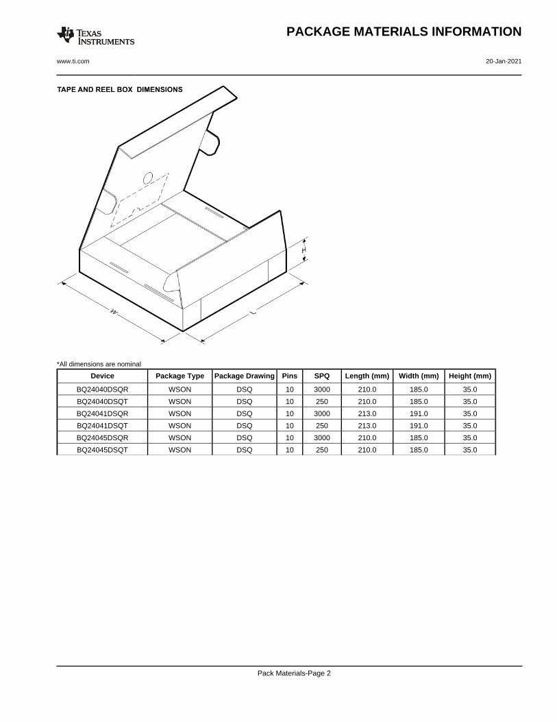
*All dimensions are nominal
Device Package Type Package Drawing Pins SPQ Length (mm) Width (mm) Height (mm)
BQ24040DSQR WSON DSQ 10 3000 210.0 185.0 35.0
BQ24040DSQT WSON DSQ 10 250 210.0 185.0 35.0
BQ24041DSQR WSON DSQ 10 3000 213.0 191.0 35.0
BQ24041DSQT WSON DSQ 10 250 213.0 191.0 35.0
BQ24045DSQR WSON DSQ 10 3000 210.0 185.0 35.0
BQ24045DSQT WSON DSQ 10 250 210.0 185.0 35.0
PACKAGE MATERIALS INFORMATION
www.ti.com 20-Jan-2021
Pack Materials-Page 2

www.ti.com
PACKAGE OUTLINE
C
2.11.9
2.11.9
0.80.7
0.050.00
2X 1.6
8X 0.4
10X 0.40.2
10X 0.250.15
1.5 0.1
0.9 0.1
(0.2) TYP
WSON - 0.8 mm max heightDSQ0010APLASTIC SMALL OUTLINE - NO LEAD
4218906/A 04/2019
0.08 C
0.1 C A B0.05
NOTES: 1. All linear dimensions are in millimeters. Any dimensions in parenthesis are for reference only. Dimensioning and tolerancing per ASME Y14.5M. 2. This drawing is subject to change without notice. 3. The package thermal pad must be soldered to the printed circuit board for thermal and mechanical performance.
PIN 1 INDEX AREA
SEATING PLANE
PIN 1 ID
SYMMEXPOSEDTHERMAL PAD
SYMM
1
5 6
10
11
SCALE 5.000
AB
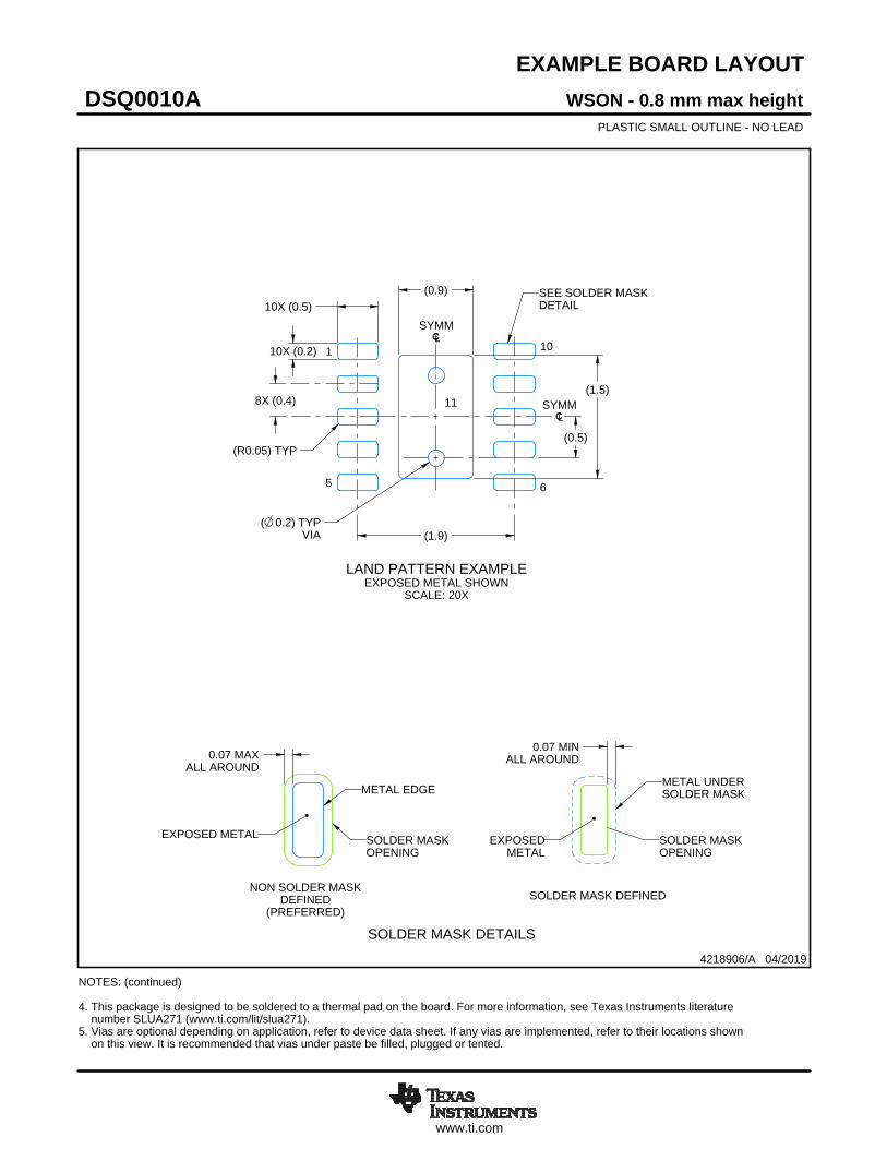
www.ti.com
EXAMPLE BOARD LAYOUT
8X (0.4)
(0.5)(R0.05) TYP
0.07 MAXALL AROUND
0.07 MINALL AROUND
10X (0.5)
10X (0.2)
(1.9)
(1.5)
(0.9)
( 0.2) TYPVIA
WSON - 0.8 mm max heightDSQ0010APLASTIC SMALL OUTLINE - NO LEAD
4218906/A 04/2019
NOTES: (continued) 4. This package is designed to be soldered to a thermal pad on the board. For more information, see Texas Instruments literature number SLUA271 (www.ti.com/lit/slua271).5. Vias are optional depending on application, refer to device data sheet. If any vias are implemented, refer to their locations shown on this view. It is recommended that vias under paste be filled, plugged or tented.
SYMM
SYMM
LAND PATTERN EXAMPLEEXPOSED METAL SHOWN
SCALE: 20X
SEE SOLDER MASKDETAIL
1
5 6
10
11
METAL EDGE
SOLDER MASKOPENING
EXPOSED METAL
METAL UNDERSOLDER MASK
SOLDER MASKOPENING
EXPOSEDMETAL
NON SOLDER MASKDEFINED
(PREFERRED)SOLDER MASK DEFINED
SOLDER MASK DETAILS

www.ti.com
EXAMPLE STENCIL DESIGN
10X (0.5)
10X (0.2)
8X (0.4)
(1.9)
(1.38)
(0.85)
(R0.05) TYP
WSON - 0.8 mm max heightDSQ0010APLASTIC SMALL OUTLINE - NO LEAD
4218906/A 04/2019
NOTES: (continued) 6. Laser cutting apertures with trapezoidal walls and rounded corners may offer better paste release. IPC-7525 may have alternate design recommendations.
SOLDER PASTE EXAMPLEBASED ON 0.125 MM THICK STENCIL
SCALE: 20X
EXPOSED PAD 1187% PRINTED SOLDER COVERAGE BY AREA UNDER PACKAGE
SYMM
SYMM
1
5 6
10
11

IMPORTANT NOTICE AND DISCLAIMERTI PROVIDES TECHNICAL AND RELIABILITY DATA (INCLUDING DATASHEETS), DESIGN RESOURCES (INCLUDING REFERENCEDESIGNS), APPLICATION OR OTHER DESIGN ADVICE, WEB TOOLS, SAFETY INFORMATION, AND OTHER RESOURCES “AS IS”AND WITH ALL FAULTS, AND DISCLAIMS ALL WARRANTIES, EXPRESS AND IMPLIED, INCLUDING WITHOUT LIMITATION ANYIMPLIED WARRANTIES OF MERCHANTABILITY, FITNESS FOR A PARTICULAR PURPOSE OR NON-INFRINGEMENT OF THIRDPARTY INTELLECTUAL PROPERTY RIGHTS.These resources are intended for skilled developers designing with TI products. You are solely responsible for (1) selecting the appropriateTI products for your application, (2) designing, validating and testing your application, and (3) ensuring your application meets applicablestandards, and any other safety, security, or other requirements. These resources are subject to change without notice. TI grants youpermission to use these resources only for development of an application that uses the TI products described in the resource. Otherreproduction and display of these resources is prohibited. No license is granted to any other TI intellectual property right or to any third partyintellectual property right. TI disclaims responsibility for, and you will fully indemnify TI and its representatives against, any claims, damages,costs, losses, and liabilities arising out of your use of these resources.TI’s products are provided subject to TI’s Terms of Sale (https:www.ti.com/legal/termsofsale.html) or other applicable terms available eitheron ti.com or provided in conjunction with such TI products. TI’s provision of these resources does not expand or otherwise alter TI’sapplicable warranties or warranty disclaimers for TI products.IMPORTANT NOTICE
Mailing Address: Texas Instruments, Post Office Box 655303, Dallas, Texas 75265Copyright © 2021, Texas Instruments Incorporated