Embed Size (px)
Citation preview
© T
his
docu
men
t is
the
excl
usiv
e pr
oper
ty o
f the
RO
BE
RT
BO
SC
H G
mbH
. With
out t
heir
cons
ent i
t may
not
be
repr
oduc
ed o
r giv
en to
third
par
ties.
BOSCH 1 279 923 771
Page - 1/72 -
Supplier: Bosch
Date of Issue: March 10/2006
Data Sheet
CJ945C
Date: March 10/2006 Dep.: AE/EIC1 Author: Lüders
No. Date
1 New edition 13.05.03
2 1 279 C03 522 Revision 08.06.04
3 1 279 C03 796 Revision 22.11.04
4 1 279 C04 069 Revision 17.06.05
5 1 279 C04 661 Revision 05.05.06
6
7
Reutlingen
BOSCH
BOSCH©
Thi
s do
cum
ent i
s th
e ex
clus
ive
prop
erty
of t
he R
OB
ER
T B
OS
CH
Gm
bH. W
ithou
t the
ir co
nsen
t it m
ay n
ot b
e re
prod
uced
or g
iven
to th
ird p
artie
s. 1 279 923 771
Page - 2/72 -
Date: March 10/2006 Dep.: AE/EIC1 Author: Lüders
Data Sheet
CJ945C Schwieberdingen
Documentation of Changes
First Revision, March 6/2003:
Second Revision, March10/2004:
- 3.4.2: IN8 High Level min=2.15V instead of 2.0V- 3.4.2: RST High Level min=2.0V instead of 1.7V- 3.10.2: FCL Low/High Time min=15ns instead 10ns- 3.4.5: max. clamping voltage bei -5mA is min=-1.5V instead -1.0V at +5mA: max=65V instead of TBD.
Note: No malfunction during clamping if the pins INx are not floating.- 1.1.1 Rons update at RT (see 3.5.5, 3.6.5, 3.7.5, 3.8.5)- 1.6.4 actual revision number is 00011000- 1.6.4 Desciption of overvoltage and reset for the bit STATUS0- 1.7 Desciption of input pins when in µsec-mode.- 1.9.1 Comment: With ohmic load - 1.10 VDD-monitoring: detailed description of the ABE-behaviour - 2.4 Electrical limits: power supply low limit is -1.0V instead of -0.5V at Ubat/VDD- 3.1, 3.2 TC with B classified- 3.5.5 RDSON max at RT is 400mΩ instead of 500mΩ- 3.6.5 RDSON max at RT is 380mΩ instead of 450mΩ- 3.7.5 RDSON max at RT is 280mΩ instead of 350mΩ- 3.8.5 RDSON max at RT is 780mΩ instead of 1000mΩ- 3.5.6, 3.6.6, 3.7.6, 3.8.6 On/Off delay time is measured with ohmic load- 3.5.7, 3.6.7, 3.7.7, 3.8.7 Leakage of power stages reduced to 10/20µA- 3.10 New note: Timing definitions are starting or ending at a voltage level of 1V
(low level) resp. 2V (high level).- 3.5.8.1 Clamping voltage is measured at 100mA instead of 200mA- 3.13.7 Suppression of Glitches (ABE): TC is B instead of A- Page 60: A new note for the maximum short circuit shut down threshold is included- Page 71: The ESD method has been changed from MIL883 to IEC 61340-3-1
3. Revision, October 11/2004:- 3.5.8.1 Clamping voltage OUT1..6. Max = 78V instead of 76V- 3.14.1 Clamping voltage:64..78V instead of 64..76V
4. Revision, May 13/2005- 3.14.3 Clamping energie @ 1.1A: 7mJ instead of 5mJ- 3.14.4 Clamping energie @ 1.0A: 40mJ instead of 30mJ- 3.13.11 load at ABE changed from 2mA to 1.5mA @ VDD=2.5V- 3.5.5 Ron OUT1..6 @ -40C: 350mΩ instead 400mΩm- 3.6.5 Ron OUT9.146 @ -40C: 300mΩ instead 380mΩ- 3.8.5 Ron OUT7,8,17,18 @ -40C: 600mΩ instead 780mΩ
5. Revision, March 10/2006- 3.4.2: IN8 High Level min=2.30V instead of 2.15V at VDD=5V- 3.4.2: IN8 High Level min=2.10V at VDD=4V- 3.3.4: Input current IN8: IIN8 = 50µA max instead of 100µA

BOSCH©
Thi
s do
cum
ent i
s th
e ex
clus
ive
prop
erty
of t
he R
OB
ER
T B
OS
CH
Gm
bH. W
ithou
t the
ir co
nsen
t it m
ay n
ot b
e re
prod
uced
or g
iven
to th
ird p
artie
s. 1 279 923 771
Page - 3/72 -
Date: March 10/2006 Dep.: AE/EIC1 Author: Lüders
Data Sheet
CJ945C Schwieberdingen
Table of ContentsPage
1. Description1.1. Short Description 41.2. Block Diagram 51.3. Description of the Power Stages 61.4. Pinout 81.5. Function of Pins 101.6. SPI Interface 11
1.6.1. Serial/Parallel Control 151.6.2. Diagnostics/Encoding of Failures 19 1.6.3. Configuration 221.6.4. Other 23
1.7. µsec-Bus Interface 321.8. Unused Power Stages 341.9. Timing Diagram of the Power Outputs 351.10. VDD-Monitoring 361.11. Notes for the Application in Commercial Vehicles 391.12. Notes for the Diagnostics 401.13. Parallel Connection of Power Stages 42
2. Maximum Ratings2.1. Definition of Test Conditions 442.2. Test Coverage in Series Production 442.3. Thermal Limits 442.4. Electrical Limits 44
3. Electrical Characteristics3.1. Operating Range 463.2. Validity of Parameters 463.3. Power Consumption 473.4. Inputs of the Power Stages and Reset 473.5. Power Outputs 2.2A/70V 493.6. Power Outputs 2.2A/45V 513.7. Power Outputs 3.0A/45V 543.8. Power Outputs 1.1A/45V 573.9. SPI Interface 613.10. µsec-Bus 643.11. Diagnostics 653.12. Reverse Currents 663.13. VDD-Monitoring ABE 673.14. Clamping Energy 69
4. EMI Requirements 71
5. ESD Capability 71
6. ISO Pulses 72
7. Quality Requirements 72
BOSCH©
Thi
s do
cum
ent i
s th
e ex
clus
ive
prop
erty
of t
he R
OB
ER
T B
OS
CH
Gm
bH. W
ithou
t the
ir co
nsen
t it m
ay n
ot b
e re
prod
uced
or g
iven
to th
ird p
artie
s. 1 279 923 771
Page - 4/72 -
Date: March 10/2006 Dep.: AE/EIC1 Author: Lüders
Data Sheet
CJ945C Schwieberdingen
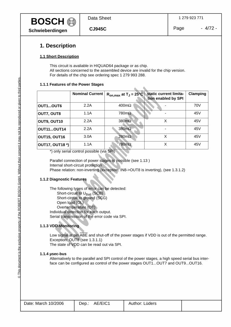
1. Description
1.1 Short Description
This circuit is avaliable in HIQUAD64 package or as chip.All sections concerned to the assembled device are invalid for the chip version.For details of the chip see ordering spec 1 279 993 288.
1.1.1 Features of the Power Stages
*) only serial control possible (via SPI)
Parallel connection of power stages is possible (see 1.13 )Internal short-circuit protectionPhase relation: non-inverting (exception: IN8->OUT8 is inverting), (see 1.3.1.2)
1.1.2 Diagnostic Features
The following types of error can be detected:Short-circuit to UBatt (SCB)Short-circuit to ground (SCG)Open load (OL)Overtemperature (OT)
Individual detection for each output.Serial transmission of the error code via SPI.
1.1.3 VDD-Monitoring
Low signal at pin ABE and shut-off of the power stages if VDD is out of the permitted range.Exception: OUT8 (see 1.3.1.1)The state of VDD can be read out via SPI.
1.1.4 µsec-busAlternatively to the parallel and SPI control of the power stages, a high speed serial bus inter-face can be configured as control of the power stages OUT1...OUT7 and OUT9...OUT16.
Nominal Current Ron,max at TJ = 25°C static current limita-tion enabled by SPI
Clamping
OUT1...OUT6 2.2A 400mΩ - 70V
OUT7, OUT8 1.1A 780mΩ - 45V
OUT9, OUT10 2.2A 380mΩ X 45V
OUT11...OUT14 2.2A 380mΩ - 45V
OUT15, OUT16 3.0A 280mΩ X 45V
OUT17, OUT18 *) 1.1A 780mΩ X 45V

BOSCH©
Thi
s do
cum
ent i
s th
e ex
clus
ive
prop
erty
of t
he R
OB
ER
T B
OS
CH
Gm
bH. W
ithou
t the
ir co
nsen
t it m
ay n
ot b
e re
prod
uced
or g
iven
to th
ird p
artie
s. 1 279 923 771
Page - 5/72 -
Date: March 10/2006 Dep.: AE/EIC1 Author: Lüders
Data Sheet
CJ945C Schwieberdingen1.2 Block Diagram
2,2A / 70V
2,2A / 70V
2,2A / 70V
2,2A / 70V
2,2A / 70V
1.1A / 45V
1.1A / 45V
2,2A / 45V
2,2A / 45V
2,2A / 45V
2,2A / 45V
2,2A / 45V
2,2A / 45V
faultdiagnostics
2,2A / 70V
UBatt
RSTSO
SCK
SSSI
OUT1
OUT3
OUT4
OUT5
OUT6
OUT2
OUT7
OUT8
OUT9
OUT10
OUT11
OUT12
OUT13
OUT14
IN1
IN2
IN3
IN4
IN5
IN6
IN7
IN8
IN11
IN12
IN13
IN14
SPI Interface
3,0A / 45V
3,0A / 45V OUT15
OUT16
1.1A / 45V OUT18
IN16
IN9
IN10
GND1...8
ABE
GND_ABE
VDDVDD-Moni-toring
VDD
control only via SPI possible
control only via SPI possible 1.1A / 45V OUT17
IN15
SPI
µsec - Bus
IN6 IN7 IN16
BOSCH©
Thi
s do
cum
ent i
s th
e ex
clus
ive
prop
erty
of t
he R
OB
ER
T B
OS
CH
Gm
bH. W
ithou
t the
ir co
nsen
t it m
ay n
ot b
e re
prod
uced
or g
iven
to th
ird p
artie
s. 1 279 923 771
Page - 6/72 -
Date: March 10/2006 Dep.: AE/EIC1 Author: Lüders
Data Sheet
CJ945C Schwieberdingen
1.3 Description of the Power Stages
OUT1 ... OUT66 non-inverting low side power switches for nominal currents up to 2.2A. Control is possible by input pins, by the µsec-bus or via SPI. For TJ = 25°C the on-resistance of the power switches is below 500mΩ.An integrated zener diode limits the output voltage to 70V typically.
OUT9 ... OUT146 non-inverting low side power switches for nominal currents up to 2.2A. Control is possible by input pins, by the µsec-bus or via SPI. For TJ = 25°C the on-resistance of the power switches is below 450mΩ.An integrated zener diode limits the output voltage to 45V typically.
OUT15, OUT162 non-inverting low side power switches for nominal currents up to 3.0A. Control is possible by input pins, by the µsec-bus or via SPI. For TJ = 25°C the on-resistance of the power switches is below 350mΩ.An integrated zener diode limits the output voltage to 45V typically.
OUT7, OUT8, OUT17, OUT184 low side power switches for nominal currents up to 1100mA. Stage 7 is non-inverting, Stage 8 is inverting (IN8 = ‘1’ => OUT8 is active). For the output OUT7 control is possible by the input pin, by the µsec-bus or via SPI, OUT8 is controlled by the input pin IN8 or via SPI, for the out-puts OUT17 and OUT18 control is only possible via SPI. For TJ = 25°C the on-resistance of the power switches is below 1000mΩ.An integrated zener diode limits the output voltage to 45V typically.
In order to increase the switching current or to reduce the power dissipation parallel connection of power stages is possible (for additional information see 1.13 ).The power stages are short-circuit proof:Power stages OUT1...OUT8, OUT11..14: In case of overload (SCB) they will be turned off after a given delay time. During this delay time the output current is limited by an internal current control loop. Power stages OUT9, OUT10, OUT15...OUT18:In case of SCB these power stages can be configured for a shut-down mode or for static cur-rent limitation. In the shut down mode while SCB they will behave like OUT1..8 or OUT11..14.In case of static current limitation and SCB the current is limited and the corresponding bit com-bination ist set (early warning) after a given delay time. They will not be turned off. If this condi-tion leads to an overtemperature condition, the output will be set into a low duty cycle PWM (selective thermal shut- down with restart) to prevent critical chip temperature.
There are 3 possibilities to turn the power stages on again:- turn the power stage off and on, either via serial control (SPI) or via parallel control (input pin, except outputs OUT17 and OUT18) or by the µsec-bus (except OUT8, OUT17,OUT18)- applying a reset signal.- sending the instruction “del_dia” by the spi-interfaceThe VDD-monitoring locks all power stages, except OUT8 for access by the IN8 input.(see 1.3.1.1)

BOSCH©
Thi
s do
cum
ent i
s th
e ex
clus
ive
prop
erty
of t
he R
OB
ER
T B
OS
CH
Gm
bH. W
ithou
t the
ir co
nsen
t it m
ay n
ot b
e re
prod
uced
or g
iven
to th
ird p
artie
s. 1 279 923 771
Page - 7/72 -
Date: March 10/2006 Dep.: AE/EIC1 Author: Lüders
Data Sheet
CJ945C Schwieberdingen
All low side switches are equipped with fault diagnostic functions:
- short-circuit to UBatt: (SCB) can be detected if switches are turned on- short-circuit to ground: (SCG) can be detected if switches are turned off- open load: (OL) can be detected if switches are turned off- overtemperature: (OT) will only be detected if switches are turned on
The fault conditions SCB, SCG, OL and OT will not be stored until an integrated filtering time is expired (please note for PWM application). If, at one output, several errors occur in a sequence, always the last detected error will be stored (with filtering time). All fault conditions are encoded in two bits per switch and are stored in the corresponding SPI registers. Additio-nally there are two central diagnostic bits: one specially for OT and one for fault occurance at any output.
The registers can be read out via SPI. After each read out cycle the registers have to be clea-red by the DEL_DIA command.
1.3.1 Power Stage OUT8 (Condensed Description)
1.3.1.1 Control of OUT8 and VDD-MonitoringOUT8 can be controlled by SPI or by the pin IN8 only, control by µs-bus is not possible. Whencontrolled by IN8 this power stage is functional if the voltage at the pin VDD is above 3,5V. InSPI mode the power stage is fully supervised by the VDD-monitor.If OUT8 is controlled by IN8, OUT8 will only be switched off by the overvoltage detection andnot by undervoltage detection.
1.3.1.2 Phase Relation IN8 - OUT8The phase relation IN8 -> OUT8 is inverting.OUT8 is active if IN8 is set to logic '1' (high level, see 3.4.2 ) in case of parallel access.On executing the read instruction on RD_INP1/2 the inverted status of IN8 is read back.
1.3.1.3 Reset / Power Stage DiagnosticsIf OUT8 is controlled by IN8, OUT8 will not be reseted by RST.After reset parallel control (by IN8) is active for OUT8.If UVDD < 4.5V errors are not stored because of the active RST of the external Regulator.Nevertheless OUT8 is protected against overload.
1.3.1.4 Input CurrentThe control input IN8 has an internal pull-down current source. Thus the input currents I IN8are positive (flow into the pin).
1.3.1.5 On ResistanceFor OUT8 and 3.5V < UVDD < 4.5V R on increases (see 3.8.5).
1.3.1.6 Parallel Connection of Power StagesParallel connection of power stages with OUT8 and parallel control is prohibited (invertinginput IN8). Control via SPI is possible. See 1.13

BOSCH©
Thi
s do
cum
ent i
s th
e ex
clus
ive
prop
erty
of t
he R
OB
ER
T B
OS
CH
Gm
bH. W
ithou
t the
ir co
nsen
t it m
ay n
ot b
e re
prod
uced
or g
iven
to th
ird p
artie
s. 1 279 923 771
Page - 8/72 -
Date: March 10/2006 Dep.: AE/EIC1 Author: Lüders
Data Sheet
CJ945C Schwieberdingen
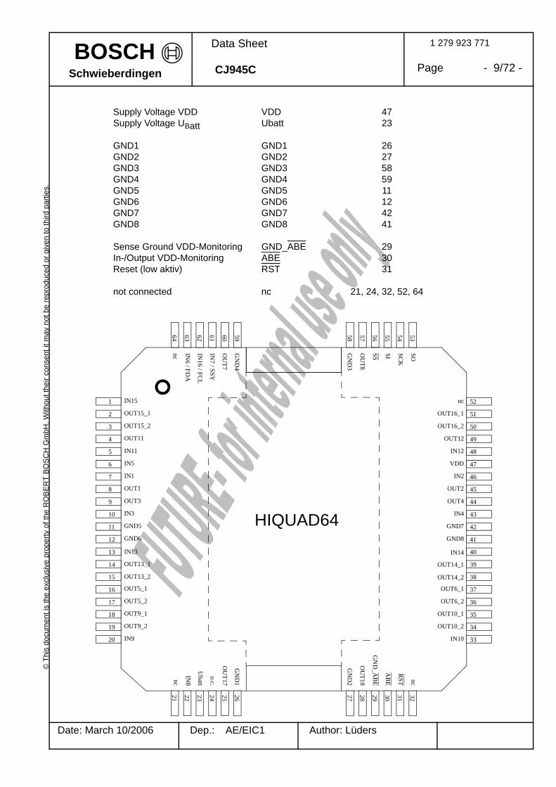
1.4 Pinout
Function Pin Pin NumberInput 1 IN1 7Input 2 IN2 46Input 3 IN3 10Input 4 IN4 43Input 5 IN5 6Input 6 or FDA IN6 63Input 7 or SSY IN7 61Input 8 IN8 22Input 9 IN9 20Input 10 IN10 33Input 11 IN11 5Input 12 IN12 48Input 13 IN13 13Input 14 IN14 40Input 15 IN15 1Input 16 or FCL IN16 62
Output 1 OUT1 8Output 2 OUT2 45Output 3 OUT3 9Output 4 OUT4 44Output 5_1 OUT5_1 16Output 5_2 OUT5_2 17Output 6_1 OUT6_1 37Output 6_2 OUT6_2 36Output 7 OUT7 60Output 8 OUT8 57Output 9_1 OUT9_1 18Output 9_2 OUT9_2 19Output 10_1 OUT10_1 35Output 10_2 OUT10_2 34Output 11 OUT11 4Output 12 OUT12 49Output 13_1 OUT13_1 14Output 13_2 OUT13_2 15Output 14_1 OUT14_1 39Output 14_2 OUT14_2 38Output 15_1 OUT15_1 2Output 15_2 OUT15_2 3Output 16_1 OUT16_1 51Output 16_2 OUT16_2 50Output 17 OUT17 25Output 18 OUT18 28(Note: OUTxy_1 and OUTxy_2 have to be connected externally!)
Slave Select SS 56Serial Output SO 53Serial Input SI 55SPI Clock SCK 54
BOSCH©
Thi
s do
cum
ent i
s th
e ex
clus
ive
prop
erty
of t
he R
OB
ER
T B
OS
CH
Gm
bH. W
ithou
t the
ir co
nsen
t it m
ay n
ot b
e re
prod
uced
or g
iven
to th
ird p
artie
s. 1 279 923 771
Page - 9/72 -
Date: March 10/2006 Dep.: AE/EIC1 Author: Lüders
Data Sheet
CJ945C Schwieberdingen
Supply Voltage VDD VDD 47Supply Voltage UBatt Ubatt 23
GND1 GND1 26GND2 GND2 27GND3 GND3 58GND4 GND4 59GND5 GND5 11GND6 GND6 12GND7 GND7 42GND8 GND8 41
Sense Ground VDD-Monitoring GND_ABE 29In-/Output VDD-Monitoring ABE 30Reset (low aktiv) RST 31
not connected nc 21, 24, 32, 52, 64
OUT6_1
20
OUT5_1
19
VDD
18
IN5
17
OUT12
16
OUT11
15
14
GND8
13
GND6 12
OUT14_2
11
OUT13_2
10
OUT2
9
OUT1 8
OUT4
7
OUT3
6
OUT10_1
5
OUT9_1
4
OUT6_2
3
OUT5_2
2
IN1
1 52
IN9
51
IN10
50
OUT9_2
49
OUT10_2
48
GND5
47
GND7
46
IN13
45
IN14
44
OUT13_1
43
OUT14_1
42
41
40
IN3
39
IN4
38
37
OUT15_2
36
OUT16_2
35
IN15
34
nc
33
nc64
IN8
63
Ubatt
62
n.c.61
OU
T1760
GN
D4
59
GN
D3
58
OU
T1857 56 55 54 53
IN6 / FD
A
21
IN16 / FC
L
22
IN7 / SSY
23
OU
T7
24 25
GN
D1
26 27 28 29 30 31 32
GN
D2
OU
T8
SCK
SISSG
ND
_AB
E
AB
E
RST nc
SOnc
OUT15_1
IN12IN11
OUT16_1
IN2
HIQUAD64

BOSCH©
Thi
s do
cum
ent i
s th
e ex
clus
ive
prop
erty
of t
he R
OB
ER
T B
OS
CH
Gm
bH. W
ithou
t the
ir co
nsen
t it m
ay n
ot b
e re
prod
uced
or g
iven
to th
ird p
artie
s. 1 279 923 771
Page - 10/72 -
Date: March 10/2006 Dep.: AE/EIC1 Author: Lüders
Data Sheet
CJ945C Schwieberdingen
1.5 Function of Pins
IN1 to IN16 Control inputs of the power stages
Internal pull-up current sources (exception: IN8 with pull-down current source)
FCL Clock for the µsec-bus (pin shared with IN16)FDA Data for the µsec-bus (pin shared with IN6)SSY Strobe and Synchronisation for the µsec-bus (pin shared with IN7)
OUT1 to OUT18 Outputs of the power switches
Short-circuit proofLow side switchesLimitation of the output voltage by zener diodes
VDD Supply voltage 5V
UBatt Supply voltage UBatt
Pin must not be left open but has to be connected either to UBatt or to VDD (e.g. in commercial vehicles)
GND1 to GND8 Ground pins
Ground pins for the power stages (see 2.4) Ground reference of all logic signals is GND1/2
RST Reset
Active lowLocks all power switches regardless of their input signals (except OUT8)Clears the fault registersResets the µsec-bus interface registers
ABE In-/Output VDD-Monitoring
Active lowOutput pin for the VDD-MonitoringInput pin for the shut-off signal coming from the supervisor
GND_ABE Sense ground VDD-Monitoring
SI, SO, SCK, SS SPI Interface

BOSCH©
Thi
s do
cum
ent i
s th
e ex
clus
ive
prop
erty
of t
he R
OB
ER
T B
OS
CH
Gm
bH. W
ithou
t the
ir co
nsen
t it m
ay n
ot b
e re
prod
uced
or g
iven
to th
ird p
artie
s. 1 279 923 771
Page - 11/72 -
Date: March 10/2006 Dep.: AE/EIC1 Author: Lüders
Data Sheet
CJ945C Schwieberdingen
1.6 SPI Interface
The serial SPI interface establishes a communication link between CJ945C and the systemsmicrocontroller. CJ945C always operates in slave mode whereas the controller provides the ma-ster function. The maximum baud rate is 5 MBaud.The CJ945C is selected by the SPI master by an active slave select signal at SS and by the firsttwo bits of the SPI instruction.SI is the data input (Slave In), SO the data output (Slave Out). ViaSCK (Serial Clock Input) the SPI clock is provided by the master.In case of inactive slave select signal (High) the data output SO goes into tristate.
Block Diagram:
SPI Control:
SO
SCK
SI
SS
Power Stages 1..16
State Machine
Shift Register
Power Stages 1..18
MUX_REG1,2SCON_REG1...3
Clock CounterControl BitsParity Generator
Power Stages 1..18
STATCON_REG DIA_REG1...5
VDD-Monitoring

BOSCH©
Thi
s do
cum
ent i
s th
e ex
clus
ive
prop
erty
of t
he R
OB
ER
T B
OS
CH
Gm
bH. W
ithou
t the
ir co
nsen
t it m
ay n
ot b
e re
prod
uced
or g
iven
to th
ird p
artie
s. 1 279 923 771
Page - 12/72 -
Date: March 10/2006 Dep.: AE/EIC1 Author: Lüders
Data Sheet
CJ945C Schwieberdingen
A SPI communication always starts with a SPI instruction sent from the controller to CJ945C.During a write cycle the controller sends the data after the SPI instruction, beginning with theMSB. During a reading cycle, after having received the SPI instruction, CJ945C sends the cor-responding data to the controller, also starting with the MSB.
SPI Command/Format:
Characteristics of the SPI Interface:
1) If the slave select signal at SS is High, the SPI-logic is set on default condition, i.e. it expectsan instruction.
2) If the 5V-reset (RST) is active, the SPI output SO is switched into tristate.The VDD monitoring (ABE) has no influence on the SPI interface.
3) Verification byte:Simultaneously to the receipt of an SPI instruction CJ945C transmits a verification byte via the output SO to the controller. This byte indicates regular or irregular operation of the SPI. It contains an initial bitpattern and a flag indicating an invalid instruction of the previous access.
4) On a read access the databits at the SPI input SI are rejected. On a writing access or afterthe DEL_DIA instruction the CJ945C sets the SPI output SO to low after sending theverification byte. If more than 16 bits are received the rest of the frame is rejected.
5) Invalid instruction/access:An instruction is invalid, if one of the following conditions is fulfilled: - an unused instruction code is detected (see tables with SPI instructions)- in case the previous transmission is not completed in terms of internal data processing- number of SPI clock pulses counted during active SS differs from exactly 16 clock pulses. A write access and the instruction DEL_DIA is internally suppressed (i.e internal registers will not be affected) in all cases where at the rising (inactive) edge of SS the number of falling edges applied to the SPI input SCK during the access is not equal to 16. A write access is also internally suppressed (i.e internal registers will not be affected) if at the rising (inactive) edge of SS a 17th bit is submitted (SCK=‘1’).
After the bits CPAD1,0 and INSTR (4-0) have been sent from the microcontroller CJ945C is able to check if the instruction code is valid. If an invalid instruction is detected, any modification on a register of CJ945C is not allowed and the databyte ‘FFh’ is transmitted after having sent the verification byte. If a valid read instruction is detected the content of the corresponding register is transmitted to the controller after having sent the verification byte (even if bit INSW afterwards is wrong). If a valid write instruction is
MSB7 6 5 4 3 2 1 0
0 0 INSTR4 INSTR3 INSTR2 INSTR1 INSTR0 INSW
Bit Name Description
7,6 CPAD1,0 Chip Adress (has to be ‘0’, ‘0’)
5-1 INSTR (4-0) SPI instruction (encoding)
0 INSW Parity of the instruction

BOSCH©
Thi
s do
cum
ent i
s th
e ex
clus
ive
prop
erty
of t
he R
OB
ER
T B
OS
CH
Gm
bH. W
ithou
t the
ir co
nsen
t it m
ay n
ot b
e re
prod
uced
or g
iven
to th
ird p
artie
s. 1 279 923 771
Page - 13/72 -
Date: March 10/2006 Dep.: AE/EIC1 Author: Lüders
Data Sheet
CJ945C Schwieberdingen
detected the data byte ’00h’ is transmitted to the controller after having sent the verificationbyte (even if bit INSW afterwards is wrong) but modifications on any register of CJ945C are
not allowed until bit INSW is valid, too.
If an invalid instruction is detected bit TRANS_F in the following verification byte is set to’High’. This bit must not be cleared before it has been sent to the microcontroller.
6) If CJ945C and additional IC’s are connected to one common slave select, they are distinguis-hed by the chip address (CPAD1, CPAD0). If an IC with 32bit-transmission-formatis selected, CJ945C must not be activated, even if slave select is set to ’low’ and the first two bits of the third byte of the 32bit-transmission are identical to the chip address of CJ945C.During the transmission of CPAD1 and CPAD0 the data output SO remains in tristate (seetiming diagram of the SPI in chapter 3.9).
SPI access format:
Verification byte:
MSB 7 6 5 4 3 2 1 0
Z Z 1 0 1 0 1 TRANS_F
Bit Name Description
0 TRANS_F Bit = 1: error detected during previous transfer Bit = 0: previous transfer was recognised as valid State after reset: 0
1 Fixed to High
2 Fixed to Low
3 Fixed to High
4 Fixed to Low
5 Fixed to High
6 send as high impedance
7 send as high impedance
MSB
SPI instruction
SS
SI
SO
MSB
Data 8bit
Check byte 00 00 00 00
MSB
SPI instruction XX XX XX XX
MSB
Data 8bit
READ-access (16bit)8 bit command + 8bit data
SS
SI
SOZZ + 6bit
Check byteZZ + 6bit
Z=tristate
WRITE-access (16bit)8 bit command + 8bit data
BOSCH©
Thi
s do
cum
ent i
s th
e ex
clus
ive
prop
erty
of t
he R
OB
ER
T B
OS
CH
Gm
bH. W
ithou
t the
ir co
nsen
t it m
ay n
ot b
e re
prod
uced
or g
iven
to th
ird p
artie
s. 1 279 923 771
Page - 14/72 -
Date: March 10/2006 Dep.: AE/EIC1 Author: Lüders
Data Sheet
CJ945C Schwieberdingen
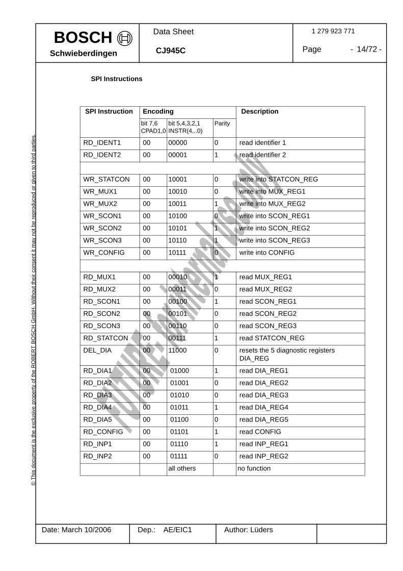
SPI Instructions
SPI Instruction Encoding Description
bit 7,6CPAD1,0
bit 5,4,3,2,1INSTR(4...0)
Parity
RD_IDENT1 00 00000 0 read identifier 1
RD_IDENT2 00 00001 1 read identifier 2
WR_STATCON 00 10001 0 write into STATCON_REG
WR_MUX1 00 10010 0 write into MUX_REG1
WR_MUX2 00 10011 1 write into MUX_REG2
WR_SCON1 00 10100 0 write into SCON_REG1
WR_SCON2 00 10101 1 write into SCON_REG2
WR_SCON3 00 10110 1 write into SCON_REG3
WR_CONFIG 00 10111 0 write into CONFIG
RD_MUX1 00 00010 1 read MUX_REG1
RD_MUX2 00 00011 0 read MUX_REG2
RD_SCON1 00 00100 1 read SCON_REG1
RD_SCON2 00 00101 0 read SCON_REG2
RD_SCON3 00 00110 0 read SCON_REG3
RD_STATCON 00 00111 1 read STATCON_REG
DEL_DIA 00 11000 0 resets the 5 diagnostic registers DIA_REG
RD_DIA1 00 01000 1 read DIA_REG1
RD_DIA2 00 01001 0 read DIA_REG2
RD_DIA3 00 01010 0 read DIA_REG3
RD_DIA4 00 01011 1 read DIA_REG4
RD_DIA5 00 01100 0 read DIA_REG5
RD_CONFIG 00 01101 1 read CONFIG
RD_INP1 00 01110 1 read INP_REG1
RD_INP2 00 01111 0 read INP_REG2
all others no function

BOSCH©
Thi
s do
cum
ent i
s th
e ex
clus
ive
prop
erty
of t
he R
OB
ER
T B
OS
CH
Gm
bH. W
ithou
t the
ir co
nsen
t it m
ay n
ot b
e re
prod
uced
or g
iven
to th
ird p
artie
s. 1 279 923 771
Page - 15/72 -
Date: March 10/2006 Dep.: AE/EIC1 Author: Lüders
Data Sheet
CJ945C Schwieberdingen
1.6.1 Serial/Parallel Control
Serial/Parallel Control of the Power Stages 1...16 and Serial Control (SPI) of the Power Stages 17 and 18:The registers MUX_REG1/2 and the bmux-bit prescribe parallel control or serial control (SPI or µsec-bus) of the power stages.
(SPI-Instuctions: WR_MUX1...2, RD_MUX1...2, WR_SCON1...3, RD_SCON1...3)
The following table shows the truth table for the control of the power stages 1...18. The registers MUX_REG1, 2 prescribe parallel-control or serial control of the power stages. The registers SCON_REG1...3 prescribe the state of the power stage in case of SPI-serial control. BMUX de-termines parallel control or control by µsec-bus.For the power stages 17 and 18 control is exclusively possible via SCON17/18. IN17/18 and MUX17/18 do not exist. BMUX has no function for OUT17/18.
Exception: OUT8 is on (active) if IN8 is set to logic ‘1’ (and off if IN8 ist set to logic ‘0’) in case ofparallel access.OUT8 can not be controled by µsec-bus! (see 1.7)
ABE RST INx BMUX MUXx SCONx µsec-REGx
Output OUTx of Power Stage x, x = 1..18
0 0 X X X X X OUTx off
0 1 X X X X X OUTx off
1 0 X X X X X OUTx off
1 1 X X 0 0 X SPI Control: OUTx on
1 1 X X 0 1 X SPI Control: OUTx off
1 1 0 1 1 X X Parallel Control: OUTx on
1 1 1 1 1 X X Parallel Control: OUTx off
1 1 X 0 1 X 0 µsec-bus Control: OUTx on
1 1 X 0 1 X 1 µsec-bus Control: OUTx off
BOSCH©
Thi
s do
cum
ent i
s th
e ex
clus
ive
prop
erty
of t
he R
OB
ER
T B
OS
CH
Gm
bH. W
ithou
t the
ir co
nsen
t it m
ay n
ot b
e re
prod
uced
or g
iven
to th
ird p
artie
s. 1 279 923 771
Page - 16/72 -
Date: March 10/2006 Dep.: AE/EIC1 Author: Lüders
Data Sheet
CJ945C Schwieberdingen
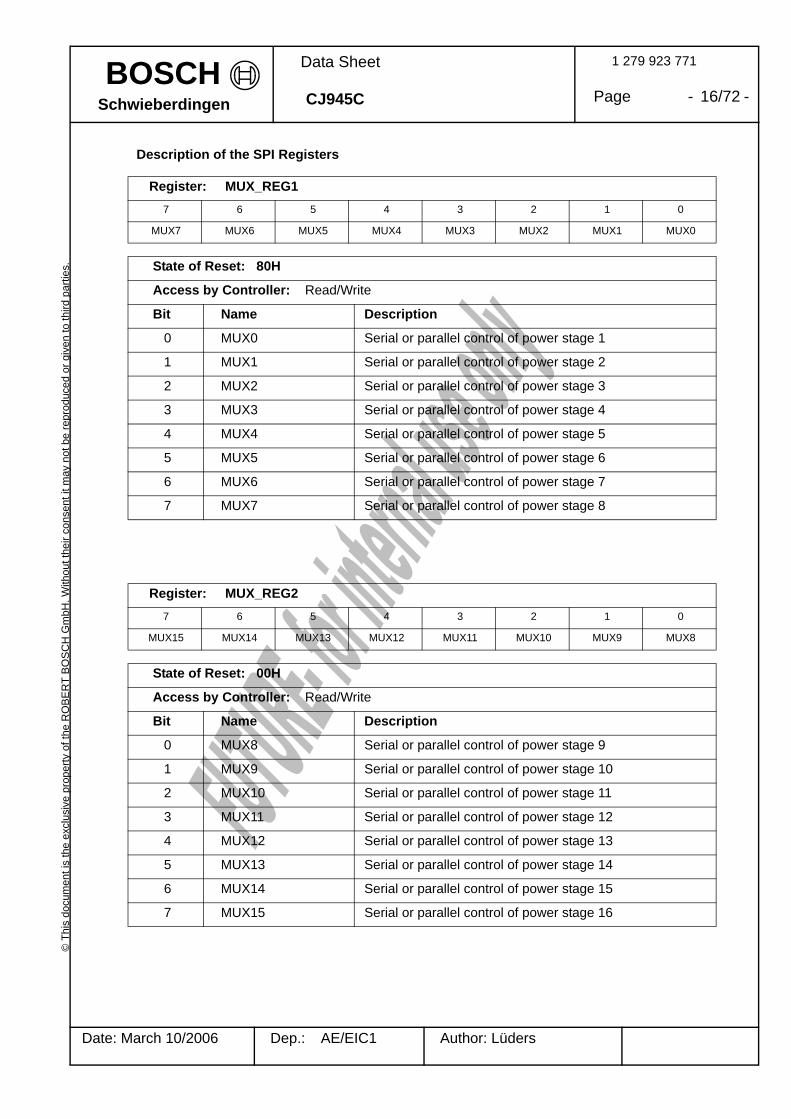
Description of the SPI Registers
Register: MUX_REG17 6 5 4 3 2 1 0
MUX7 MUX6 MUX5 MUX4 MUX3 MUX2 MUX1 MUX0
State of Reset: 80H
Access by Controller: Read/Write
Bit Name Description
0 MUX0 Serial or parallel control of power stage 1
1 MUX1 Serial or parallel control of power stage 2
2 MUX2 Serial or parallel control of power stage 3
3 MUX3 Serial or parallel control of power stage 4
4 MUX4 Serial or parallel control of power stage 5
5 MUX5 Serial or parallel control of power stage 6
6 MUX6 Serial or parallel control of power stage 7
7 MUX7 Serial or parallel control of power stage 8
Register: MUX_REG27 6 5 4 3 2 1 0
MUX15 MUX14 MUX13 MUX12 MUX11 MUX10 MUX9 MUX8
State of Reset: 00H
Access by Controller: Read/Write
Bit Name Description
0 MUX8 Serial or parallel control of power stage 9
1 MUX9 Serial or parallel control of power stage 10
2 MUX10 Serial or parallel control of power stage 11
3 MUX11 Serial or parallel control of power stage 12
4 MUX12 Serial or parallel control of power stage 13
5 MUX13 Serial or parallel control of power stage 14
6 MUX14 Serial or parallel control of power stage 15
7 MUX15 Serial or parallel control of power stage 16
BOSCH©
Thi
s do
cum
ent i
s th
e ex
clus
ive
prop
erty
of t
he R
OB
ER
T B
OS
CH
Gm
bH. W
ithou
t the
ir co
nsen
t it m
ay n
ot b
e re
prod
uced
or g
iven
to th
ird p
artie
s. 1 279 923 771
Page - 17/72 -
Date: March 10/2006 Dep.: AE/EIC1 Author: Lüders
Data Sheet
CJ945C Schwieberdingen
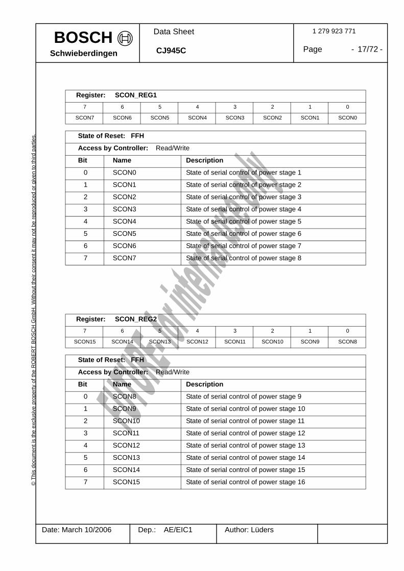
Register: SCON_REG17 6 5 4 3 2 1 0
SCON7 SCON6 SCON5 SCON4 SCON3 SCON2 SCON1 SCON0
State of Reset: FFH
Access by Controller: Read/Write
Bit Name Description
0 SCON0 State of serial control of power stage 1
1 SCON1 State of serial control of power stage 2
2 SCON2 State of serial control of power stage 3
3 SCON3 State of serial control of power stage 4
4 SCON4 State of serial control of power stage 5
5 SCON5 State of serial control of power stage 6
6 SCON6 State of serial control of power stage 7
7 SCON7 State of serial control of power stage 8
Register: SCON_REG27 6 5 4 3 2 1 0
SCON15 SCON14 SCON13 SCON12 SCON11 SCON10 SCON9 SCON8
State of Reset: FFH
Access by Controller: Read/Write
Bit Name Description
0 SCON8 State of serial control of power stage 9
1 SCON9 State of serial control of power stage 10
2 SCON10 State of serial control of power stage 11
3 SCON11 State of serial control of power stage 12
4 SCON12 State of serial control of power stage 13
5 SCON13 State of serial control of power stage 14
6 SCON14 State of serial control of power stage 15
7 SCON15 State of serial control of power stage 16
BOSCH©
Thi
s do
cum
ent i
s th
e ex
clus
ive
prop
erty
of t
he R
OB
ER
T B
OS
CH
Gm
bH. W
ithou
t the
ir co
nsen
t it m
ay n
ot b
e re
prod
uced
or g
iven
to th
ird p
artie
s. 1 279 923 771
Page - 18/72 -
Date: March 10/2006 Dep.: AE/EIC1 Author: Lüders
Data Sheet
CJ945C Schwieberdingen
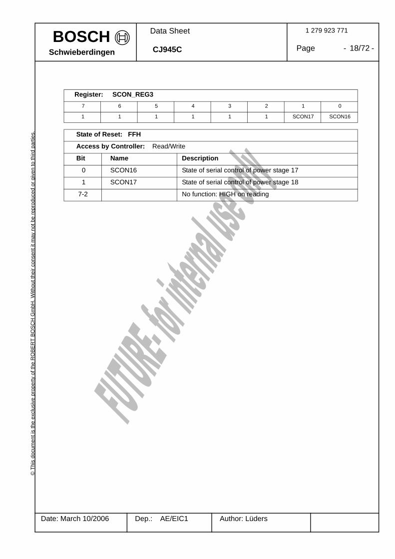
Register: SCON_REG37 6 5 4 3 2 1 0
1 1 1 1 1 1 SCON17 SCON16
State of Reset: FFH
Access by Controller: Read/Write
Bit Name Description
0 SCON16 State of serial control of power stage 17
1 SCON17 State of serial control of power stage 18
7-2 No function: HIGH on reading
BOSCH©
Thi
s do
cum
ent i
s th
e ex
clus
ive
prop
erty
of t
he R
OB
ER
T B
OS
CH
Gm
bH. W
ithou
t the
ir co
nsen
t it m
ay n
ot b
e re
prod
uced
or g
iven
to th
ird p
artie
s. 1 279 923 771
Page - 19/72 -
Date: March 10/2006 Dep.: AE/EIC1 Author: Lüders
Data Sheet
CJ945C Schwieberdingen
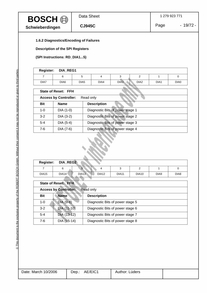
1.6.2 Diagnostics/Encoding of Failures
Description of the SPI Registers
(SPI Instructions: RD_DIA1...5)
Register: DIA_REG17 6 5 4 3 2 1 0
DIA7 DIA6 DIA5 DIA4 DIA3 DIA2 DIA1 DIA0
State of Reset: FFH
Access by Controller: Read only
Bit Name Description
1-0 DIA (1-0) Diagnostic Bits of power stage 1
3-2 DIA (3-2) Diagnostic Bits of power stage 2
5-4 DIA (5-4) Diagnostic Bits of power stage 3
7-6 DIA (7-6) Diagnostic Bits of power stage 4
Register: DIA_REG27 6 5 4 3 2 1 0
DIA15 DIA14 DIA13 DIA12 DIA11 DIA10 DIA9 DIA8
State of Reset: FFH
Access by Controller: Read only
Bit Name Description
1-0 DIA (9-8) Diagnostic Bits of power stage 5
3-2 DIA (11-10) Diagnostic Bits of power stage 6
5-4 DIA (13-12) Diagnostic Bits of power stage 7
7-6 DIA (15-14) Diagnostic Bits of power stage 8

BOSCH©
Thi
s do
cum
ent i
s th
e ex
clus
ive
prop
erty
of t
he R
OB
ER
T B
OS
CH
Gm
bH. W
ithou
t the
ir co
nsen
t it m
ay n
ot b
e re
prod
uced
or g
iven
to th
ird p
artie
s. 1 279 923 771
Page - 20/72 -
Date: March 10/2006 Dep.: AE/EIC1 Author: Lüders
Data Sheet
CJ945C Schwieberdingen
Register: DIA_REG37 6 5 4 3 2 1 0
DIA23 DIA22 DIA21 DIA20 DIA19 DIA18 DIA17 DIA16
State of Reset: FFH
Access by Controller: Read only
Bit Name Description
1-0 DIA (17-16) Diagnostic Bits of power stage 9
3-2 DIA (19-18) Diagnostic Bits of power stage 10
5-4 DIA (21-20) Diagnostic Bits of power stage 11
7-6 DIA (23-22) Diagnostic Bits of power stage 12
Register: DIA_REG47 6 5 4 3 2 1 0
DIA31 DIA30 DIA29 DIA28 DIA27 DIA26 DIA25 DIA24
State of Reset: FFH
Access by Controller: Read only
Bit Name Description
1-0 DIA (25-24) Diagnostic Bits of power stage 13
3-2 DIA (27-26) Diagnostic Bits of power stage 14
5-4 DIA (29-28) Diagnostic Bits of power stage 15
7-6 DIA (31-30) Diagnostic Bits of power stage 16
BOSCH©
Thi
s do
cum
ent i
s th
e ex
clus
ive
prop
erty
of t
he R
OB
ER
T B
OS
CH
Gm
bH. W
ithou
t the
ir co
nsen
t it m
ay n
ot b
e re
prod
uced
or g
iven
to th
ird p
artie
s. 1 279 923 771
Page - 21/72 -
Date: March 10/2006 Dep.: AE/EIC1 Author: Lüders
Data Sheet
CJ945C Schwieberdingen
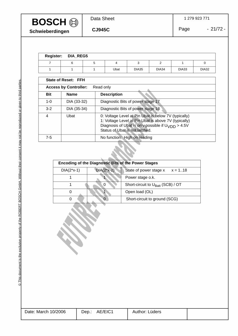
Register: DIA_REG57 6 5 4 3 2 1 0
1 1 1 Ubat DIA35 DIA34 DIA33 DIA32
State of Reset: FFH
Access by Controller: Read only
Bit Name Description
1-0 DIA (33-32) Diagnostic Bits of power stage 17
3-2 DIA (35-34) Diagnostic Bits of power stage 18
4 Ubat 0: Voltage Level at Pin Ubat is below 7V (typically) 1: Voltage Level at Pin Ubat is above 7V (typically) Diagnosis of Ubat is only possible if UVDD > 4.5V Status of Ubat is not latched.
7-5 No function: High on reading
Encoding of the Diagnostic Bits of the Power Stages
DIA(2*x-1) DIA(2*x-2) State of power stage x x = 1..18
1 1 Power stage o.k.
1 0 Short-circuit to UBatt (SCB) / OT
0 1 Open load (OL)
0 0 Short-circuit to ground (SCG)

BOSCH©
Thi
s do
cum
ent i
s th
e ex
clus
ive
prop
erty
of t
he R
OB
ER
T B
OS
CH
Gm
bH. W
ithou
t the
ir co
nsen
t it m
ay n
ot b
e re
prod
uced
or g
iven
to th
ird p
artie
s. 1 279 923 771
Page - 22/72 -
Date: March 10/2006 Dep.: AE/EIC1 Author: Lüders
Data Sheet
CJ945C Schwieberdingen
1.6.3 Configuration
The µsec-bus is enabled by this register. In addition the shut off at SCB can be configured for the power-stages OUT9, OUT10 and OUT15 ... OUT18.
Description of the µsec-bus see chapter 1.7
CONFIG (Read and write) 7 6 5 4 3 2 1 0
O16-SCB O15-SCB O10-SCB O9-SCB O18-SCB O17-SCB BMUX 1
State of Reset: FFh
Bit Name Description
0 No function: HIGH on reading
1 BMUX 1: parallel inputs INx enabled 0: µsec-Bus Interface enabled
2 O17-SCB 1: The output OUT17 is switched off in case of SCB 0: The output is not switched off in case of SCB
3 O18-SCB 1: The output OUT18 is switched off in case of SCB 0: The output is not switched off in case of SCB
4 O9-SCB 1: The output OUT9 is switched off in case of SCB 0: The output is not switched off in case of SCB
5 O10-SCB 1: The output OUT10 is switched off in case of SCB 0: The output is not switched off in case of SCB
6 O15-SCB 1: The output OUT15 is switched off in case of SCB 0: The output is not switched off in case of SCB
7 O16-SCB 1: The output OUT16 is switched off in case of SCB 0: The output is not switched off in case of SCB

BOSCH©
Thi
s do
cum
ent i
s th
e ex
clus
ive
prop
erty
of t
he R
OB
ER
T B
OS
CH
Gm
bH. W
ithou
t the
ir co
nsen
t it m
ay n
ot b
e re
prod
uced
or g
iven
to th
ird p
artie
s. 1 279 923 771
Page - 23/72 -
Date: March 10/2006 Dep.: AE/EIC1 Author: Lüders
Data Sheet
CJ945C Schwieberdingen
1.6.4 Other
Reading the IC Identifier (SPI Instruction: RD_IDENT1):
Reading the IC revision number (SPI Instruction: RD_IDENT2):
Reset of the Diagnostic Information (SPI Instruction: DEL_DIA):
Resets the 5 diagnostic registers DIA_REG1...5 to FFH and the common overtemperature flag in register STATCON_REG (Bit4) to High. These bits are only cleared by the DEL_DIA instruction when there is no failure entry at the input of the registers.Access is performed like a writing access with any data byte.
In the case a power stage is shut off because of SCB, the output is activated again by the DEL_DIA instruction and the filtering-time is enabled. Therefore in case of SCB the output is activated and shut off after the shutoff delay.For a power stage in the current limitation mode, the current limitation mode is left, if a DEL_DIA instruction has been received. If there is still the condition for SCB the current limitation modeis entered again.
On the following pages the conditions for set and reset of the SCB report in DIA_REGx is shown inseveral schematics. The signal „power stage control“ is generated as follows:
IC Identifier1 (Device ID) 7 6 5 4 3 2 1 0
ID7 ID6 ID5 ID4 ID3 ID2 ID1 ID0
Bit Name Description
7...0 ID(7...0) ID-No.: 10011000 (98 hex)
IC revision number 7 6 5 4 3 2 1 0
SWR3 SWR2 SWR1 SWR0 MSR3 MSR2 MSR1 MSR0
Bit Name Description
7...4 SWR(3...0) Revision corresponding to Software release: 0001 (1Hex)
3...0 MSR(3...0) Revision corresponding to Maskset: 1000 (8Hex)
OR ANDpower stage control = „ON“ABE not activeINi=“ON“
SPI=“ON“µsec=“ON“
BOSCH©
Thi
s do
cum
ent i
s th
e ex
clus
ive
prop
erty
of t
he R
OB
ER
T B
OS
CH
Gm
bH. W
ithou
t the
ir co
nsen
t it m
ay n
ot b
e re
prod
uced
or g
iven
to th
ird p
artie
s. 1 279 923 771
Page - 24/72 -
Date: March 10/2006 Dep.: AE/EIC1 Author: Lüders
Data Sheet
CJ945C Schwieberdingen
SC
B c
ondi
tion
OU
Tx
Faul
t ent
ryin
DIA
_RE
Gx
DE
L_D
IA c
omm
and
Res
et
pow
er s
tage
SCB
t DIA
G
On
SC
BS
CB
On
On
On
On
On
SC
B
On
On
On
On
On
t DIA
Gt D
IAG
t DIA
G
Sche
mat
ic o
f SC
B re
port
of p
ower
sta
ges
OU
T1...
7,9.
..18
(pow
er s
tage
pro
gram
med
for
no S
CB
shut
-off
in c
ase
of S
CB
), SC
B e
ntry
del
eted
by
DEL
_DIA
afte
r SC
B c
ondi
tion
disa
ppea
red
and
pow
er s
tage
con
trol
was
togg
led
cont
rol

BOSCH©
Thi
s do
cum
ent i
s th
e ex
clus
ive
prop
erty
of t
he R
OB
ER
T B
OS
CH
Gm
bH. W
ithou
t the
ir co
nsen
t it m
ay n
ot b
e re
prod
uced
or g
iven
to th
ird p
artie
s. 1 279 923 771
Page - 25/72 -
Date: March 10/2006 Dep.: AE/EIC1 Author: Lüders
Data Sheet
CJ945C Schwieberdingen
Sche
mat
ic o
f SC
B re
port
of p
ower
sta
ges
OU
T1...
7,9.
..18
(pow
er s
tage
pro
gram
med
for
SC
B c
ondi
tion
SC
Bno
SC
B
OU
TxO
nO
nO
nO
nO
nO
n
Faul
t ent
ryin
DIA
_RE
Gx
SC
BS
CB
SCB
Res
et
DE
L_D
IA c
omm
and
pow
er s
tage
cont
rol
On
On
On
On
On
t DIA
Gt D
IAG
t DIA
Gt D
IAG
shut
-off
in c
ase
of S
CB
), SC
B e
ntry
del
eted
by
Res
et a
fter S
CB
con
ditio
n di
sapp
eare
dan
d po
wer
sta
ge c
ontr
ol w
as to
ggle
d
BOSCH©
Thi
s do
cum
ent i
s th
e ex
clus
ive
prop
erty
of t
he R
OB
ER
T B
OS
CH
Gm
bH. W
ithou
t the
ir co
nsen
t it m
ay n
ot b
e re
prod
uced
or g
iven
to th
ird p
artie
s. 1 279 923 771
Page - 26/72 -
Date: March 10/2006 Dep.: AE/EIC1 Author: Lüders
Data Sheet
CJ945C Schwieberdingen
Sche
mat
ic o
f SC
B re
port
of p
ower
sta
ges
OU
T1...
7,9.
..18
(pow
er s
tage
pro
gram
med
for
SC
B c
ondi
tion
SC
Bno
SC
B
OU
TxO
nO
nO
nO
nO
n
Faul
t ent
ryin
DIA
_RE
Gx
SCB
SC
BSC
B
Res
et
DE
L_D
IA c
omm
and
pow
er s
tage
cont
rol
On
On
On
t DIA
Gt D
IAG
t DIA
Gt D
IAG
On
On
shut
-off
in c
ase
of S
CB
), SC
B e
ntry
del
eted
by
DEL
_DIA
afte
r SC
B c
ondi
tion
disa
ppea
red
but p
ower
sta
ge c
ontr
ol w
as n
ot to
ggle
d
BOSCH©
Thi
s do
cum
ent i
s th
e ex
clus
ive
prop
erty
of t
he R
OB
ER
T B
OS
CH
Gm
bH. W
ithou
t the
ir co
nsen
t it m
ay n
ot b
e re
prod
uced
or g
iven
to th
ird p
artie
s. 1 279 923 771
Page - 27/72 -
Date: March 10/2006 Dep.: AE/EIC1 Author: Lüders
Data Sheet
CJ945C Schwieberdingen
Sche
mat
ic o
f SC
B re
port
of p
ower
sta
ges
OU
T1...
7,9.
..18
(pow
er s
tage
pro
gram
med
for
SC
B c
ondi
tion
SC
Bno
SC
B
OU
TxO
nO
nO
nO
nO
n
Faul
t ent
ryin
DIA
_RE
Gx
SCB
SC
BSC
B
Res
et
DE
L_D
IA c
omm
and
pow
er s
tage
cont
rol
On
On
On
t DIA
Gt D
IAG
t DIA
Gt D
IAG
On
shut
-off
in c
ase
of S
CB
), SC
B e
ntry
del
eted
by
Res
et a
fter S
CB
con
ditio
n di
sapp
eare
dbu
t pow
er s
tage
con
trol
was
not
togg
led
BOSCH©
Thi
s do
cum
ent i
s th
e ex
clus
ive
prop
erty
of t
he R
OB
ER
T B
OS
CH
Gm
bH. W
ithou
t the
ir co
nsen
t it m
ay n
ot b
e re
prod
uced
or g
iven
to th
ird p
artie
s. 1 279 923 771
Page - 28/72 -
Date: March 10/2006 Dep.: AE/EIC1 Author: Lüders
Data Sheet
CJ945C Schwieberdingen
Sche
mat
ic o
f SC
B re
port
of p
ower
sta
ges
OU
T9,1
0,15
...18
(pow
er s
tage
pro
gram
med
for
SC
B c
ondi
tion
OU
Tx
Faul
t ent
ryin
DIA
_RE
Gx
DE
L_D
IA c
omm
and
Res
et
pow
er s
tage
cont
rol
SC
B
t DIA
G
SC
BS
CB
On
On
On
On
SCB
On
On
On
On
OT
cond
ition
OT
no S
CB
no O
Tno
OT
On
t DIA
Gt D
IAG
t DIA
,OT
curr
ent l
imita
tion
in c
ase
of S
CB
), SC
B re
sp. O
T fla
g en
try
dele
ted
exem
plar
y by
DEL
_DIA
afte
r SC
B re
sp. O
T co
nditi
on d
isap
pear
ed a
nd p
ower
sta
ge c
ontr
ol w
as to
ggle
d
com
mon
OT
flag
in S
TATC
ON
_RE
G
OT
t DIA
,OT

BOSCH©
Thi
s do
cum
ent i
s th
e ex
clus
ive
prop
erty
of t
he R
OB
ER
T B
OS
CH
Gm
bH. W
ithou
t the
ir co
nsen
t it m
ay n
ot b
e re
prod
uced
or g
iven
to th
ird p
artie
s. 1 279 923 771
Page - 29/72 -
Date: March 10/2006 Dep.: AE/EIC1 Author: Lüders
Data Sheet
CJ945C Schwieberdingen
Reading Input1 (SPI Instruction: RD_INP1):
Reading Input2 (SPI Instruction: RD_INP2):
The input pins IN1..IN5 and IN8...IN15 can be used as input port expander by reading the status of the input pins by the SPI-commands RD_INP1/2. If the µsec-bus-interface is enabled (BMUX=0) the pullup current sources at the input IN1..5 and IN9..15 are disabled. If BMUX=1 the pullup current sources at these pins are enabled. The pullup/pulldown current sources of the other input pins are not effected by the bit BMUX.
On executing the read instruction on RD_INP1/2, the present status (not latched) of the input pins INx is read back (exception: bit IN8 represents the inverted status of input pin IN8).
Register INP_REG17 6 5 4 3 2 1 0
IN8 Test 0 IN5 IN4 IN3 IN2 IN1
Bit Name Description
0..4 IN(1...5) Status of the input pins IN1 ... IN5
5 No function: LOW on reading
6 Test µsec-test-bit, the bit D8 of the µsec-bus is read
7 IN8 Inverted status of the input pin IN8: Low level at pin IN8: Bit 7 = 1 High level at pin IN8: Bit 7 = 0
Register INP_REG27 6 5 4 3 2 1 0
0 IN15 IN14 IN13 IN12 IN11 IN10 IN9
Bit Name Description
0..6 IN9...IN15 Status of the input pins IN9...IN15
7 No function: LOW on reading
BOSCH©
Thi
s do
cum
ent i
s th
e ex
clus
ive
prop
erty
of t
he R
OB
ER
T B
OS
CH
Gm
bH. W
ithou
t the
ir co
nsen
t it m
ay n
ot b
e re
prod
uced
or g
iven
to th
ird p
artie
s. 1 279 923 771
Page - 30/72 -
Date: March 10/2006 Dep.: AE/EIC1 Author: Lüders
Data Sheet
CJ945C Schwieberdingen
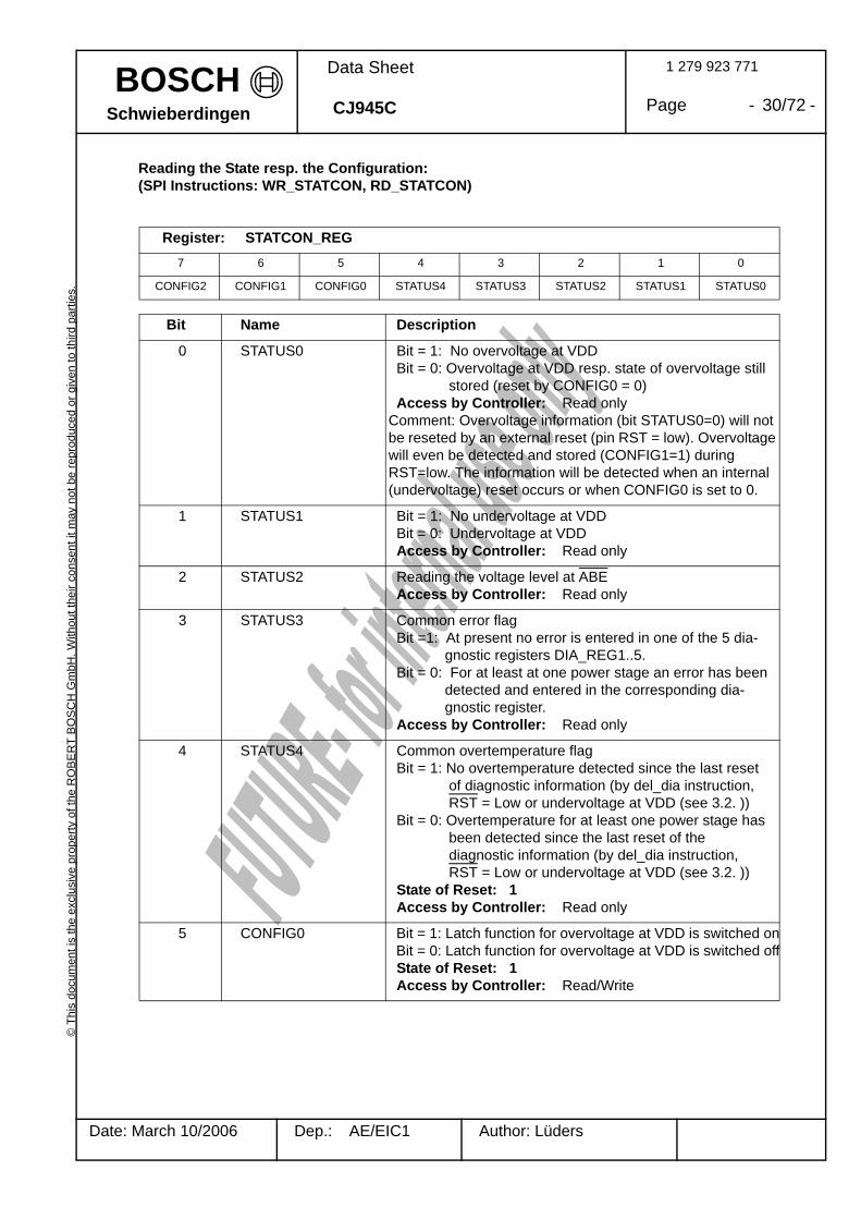
Reading the State resp. the Configuration:(SPI Instructions: WR_STATCON, RD_STATCON)
Register: STATCON_REG7 6 5 4 3 2 1 0
CONFIG2 CONFIG1 CONFIG0 STATUS4 STATUS3 STATUS2 STATUS1 STATUS0
Bit Name Description
0 STATUS0 Bit = 1: No overvoltage at VDD Bit = 0: Overvoltage at VDD resp. state of overvoltage still stored (reset by CONFIG0 = 0) Access by Controller: Read onlyComment: Overvoltage information (bit STATUS0=0) will not be reseted by an external reset (pin RST = low). Overvoltage will even be detected and stored (CONFIG1=1) during RST=low. The information will be detected when an internal (undervoltage) reset occurs or when CONFIG0 is set to 0.
1 STATUS1 Bit = 1: No undervoltage at VDD Bit = 0: Undervoltage at VDD Access by Controller: Read only
2 STATUS2 Reading the voltage level at ABE Access by Controller: Read only
3 STATUS3 Common error flag Bit =1: At present no error is entered in one of the 5 dia- gnostic registers DIA_REG1..5. Bit = 0: For at least at one power stage an error has been detected and entered in the corresponding dia- gnostic register. Access by Controller: Read only
4 STATUS4 Common overtemperature flag Bit = 1: No overtemperature detected since the last reset of diagnostic information (by del_dia instruction, RST = Low or undervoltage at VDD (see 3.2. )) Bit = 0: Overtemperature for at least one power stage has been detected since the last reset of the diagnostic information (by del_dia instruction, RST = Low or undervoltage at VDD (see 3.2. )) State of Reset: 1 Access by Controller: Read only
5 CONFIG0 Bit = 1: Latch function for overvoltage at VDD is switched on Bit = 0: Latch function for overvoltage at VDD is switched off State of Reset: 1 Access by Controller: Read/Write

BOSCH©
Thi
s do
cum
ent i
s th
e ex
clus
ive
prop
erty
of t
he R
OB
ER
T B
OS
CH
Gm
bH. W
ithou
t the
ir co
nsen
t it m
ay n
ot b
e re
prod
uced
or g
iven
to th
ird p
artie
s. 1 279 923 771
Page - 31/72 -
Date: March 10/2006 Dep.: AE/EIC1 Author: Lüders
Data Sheet
CJ945C Schwieberdingen
6 CONFIG1 Bit = 1: Lower threshold of VDD-monitoring is lifted if bit CONFIG2 = 0 (test of switch-off path) Bit = 0: Upper threshold of VDD-monitoring is reduced if bit CONFIG2 = 0 (test of switch-off path) State of Reset: 1 Access by Controller: Read/Write
7 CONFIG2 Bit = 1: Test of VDD threshold is switched off Bit = 0: Test of VDD threshold is switched on State of Reset: 1 Access by Controller: Read/Write

BOSCH©
Thi
s do
cum
ent i
s th
e ex
clus
ive
prop
erty
of t
he R
OB
ER
T B
OS
CH
Gm
bH. W
ithou
t the
ir co
nsen
t it m
ay n
ot b
e re
prod
uced
or g
iven
to th
ird p
artie
s. 1 279 923 771
Page - 32/72 -
Date: March 10/2006 Dep.: AE/EIC1 Author: Lüders
Data Sheet
CJ945C Schwieberdingen
1.7 µsec - Bus InterfaceThe µsec-bus-interface is one of three possibilities to control the powerstages. OUT1...OUT7 and OUT9...OUT16 are influenced by the reset input RST. If RST is set to Low, these power stages are switched off. After reset they are controlled by the SPI (default initialization of CJ945C). Power stage 8 however is not influenced by the reset input if it’s controlled by IN8 and UVDD > 3,5V. Alternatively these outputs can be controlled either by the pins IN1...IN16 or by the µsec-bus interface. Exception: OUT8 can be controlled by IN8 or by the SPI-interface only. The bit ’Bus-Multiplex’ (BMUX) in the SPI register CONFIG prescribes parallel access (IN1...IN7, IN9...IN16) or µsec-bus control (see figure below). Exception: If BMUX is set to ‘0’ only the power-stages OUT1...OUT7 and OUT9...OUT16 are controlled by the µsec-bus.
Main features:- 16 data bits for each data-frame (at the pin FDA)- 16 clock-pulses for each data-frame (at the pin FCL)- clock frequency: 0...20 MHz- one sync -input (pin SSY) to latch the input data stream- input level interface same as for IN6, IN7, IN16- no error correction
SSY
FCL
D0 D1 don’t careD15D14
Data-Frame
FDA D0
16 bit shift registerFDAFCL
SSY
SCON_REG
Principle of the µsec-bus interface
16 bit µsec-bus Reg.
SPI-shift-regSPI
INx BMUX
MUX_REG
OUTx
BOSCH©
Thi
s do
cum
ent i
s th
e ex
clus
ive
prop
erty
of t
he R
OB
ER
T B
OS
CH
Gm
bH. W
ithou
t the
ir co
nsen
t it m
ay n
ot b
e re
prod
uced
or g
iven
to th
ird p
artie
s. 1 279 923 771
Page - 33/72 -
Date: March 10/2006 Dep.: AE/EIC1 Author: Lüders
Data Sheet
CJ945C Schwieberdingen
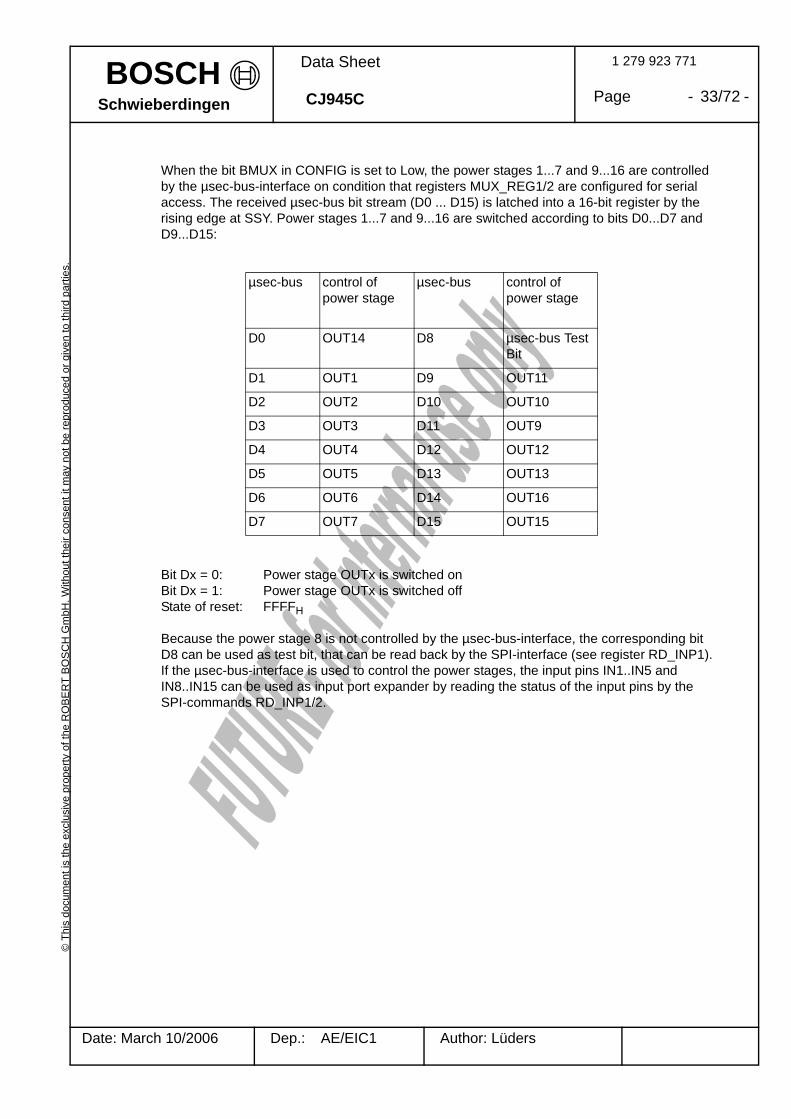
When the bit BMUX in CONFIG is set to Low, the power stages 1...7 and 9...16 are controlled by the µsec-bus-interface on condition that registers MUX_REG1/2 are configured for serial access. The received µsec-bus bit stream (D0 ... D15) is latched into a 16-bit register by the rising edge at SSY. Power stages 1...7 and 9...16 are switched according to bits D0...D7 and D9...D15:
Bit Dx = 0: Power stage OUTx is switched onBit Dx = 1: Power stage OUTx is switched offState of reset: FFFFH
Because the power stage 8 is not controlled by the µsec-bus-interface, the corresponding bit D8 can be used as test bit, that can be read back by the SPI-interface (see register RD_INP1). If the µsec-bus-interface is used to control the power stages, the input pins IN1..IN5 and IN8..IN15 can be used as input port expander by reading the status of the input pins by the SPI-commands RD_INP1/2.
µsec-bus control of power stage
µsec-bus control of power stage
D0 OUT14 D8 µsec-bus Test Bit
D1 OUT1 D9 OUT11
D2 OUT2 D10 OUT10
D3 OUT3 D11 OUT9
D4 OUT4 D12 OUT12
D5 OUT5 D13 OUT13
D6 OUT6 D14 OUT16
D7 OUT7 D15 OUT15
BOSCH©
Thi
s do
cum
ent i
s th
e ex
clus
ive
prop
erty
of t
he R
OB
ER
T B
OS
CH
Gm
bH. W
ithou
t the
ir co
nsen
t it m
ay n
ot b
e re
prod
uced
or g
iven
to th
ird p
artie
s. 1 279 923 771
Page - 34/72 -
Date: March 10/2006 Dep.: AE/EIC1 Author: Lüders
Data Sheet
CJ945C Schwieberdingen
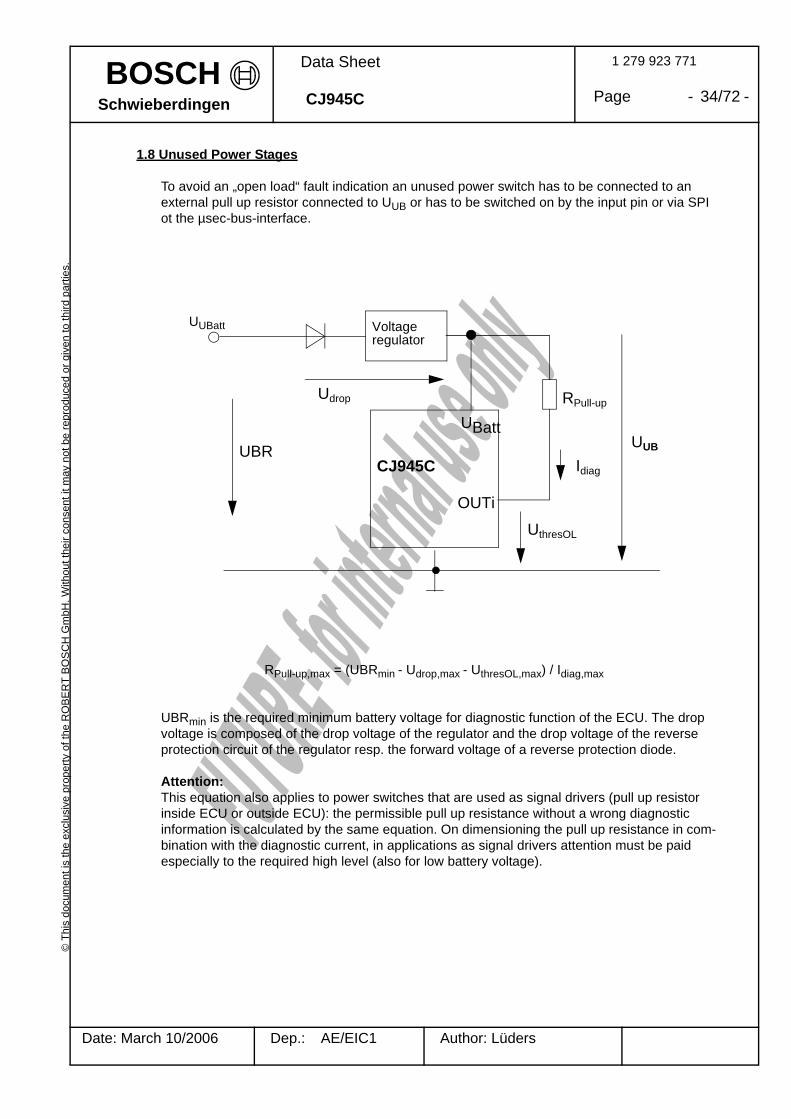
1.8 Unused Power Stages
To avoid an „open load“ fault indication an unused power switch has to be connected to an external pull up resistor connected to UUB or has to be switched on by the input pin or via SPI ot the µsec-bus-interface.
RPull-up,max = (UBRmin - Udrop,max - UthresOL,max) / Idiag,max
UBRmin is the required minimum battery voltage for diagnostic function of the ECU. The drop voltage is composed of the drop voltage of the regulator and the drop voltage of the reverse protection circuit of the regulator resp. the forward voltage of a reverse protection diode.
Attention:This equation also applies to power switches that are used as signal drivers (pull up resistor inside ECU or outside ECU): the permissible pull up resistance without a wrong diagnostic information is calculated by the same equation. On dimensioning the pull up resistance in com-bination with the diagnostic current, in applications as signal drivers attention must be paid especially to the required high level (also for low battery voltage).
CJ945C Idiag
RPull-up
UthresOL
UBR UUB
UBatt
Voltage
OUTi
Udrop
UUBattregulator
BOSCH©
Thi
s do
cum
ent i
s th
e ex
clus
ive
prop
erty
of t
he R
OB
ER
T B
OS
CH
Gm
bH. W
ithou
t the
ir co
nsen
t it m
ay n
ot b
e re
prod
uced
or g
iven
to th
ird p
artie
s. 1 279 923 771
Page - 35/72 -
Date: March 10/2006 Dep.: AE/EIC1 Author: Lüders
Data Sheet
CJ945C Schwieberdingen
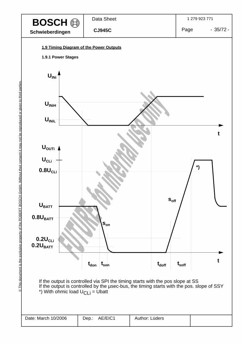
1.9 Timing Diagram of the Power Outputs
1.9.1 Power Stages
UINiH
UINiL
t
t
0.8UCLi
UINi
tdofftdon
0.8UBATT
0.2UBATT
son
soff
UCLi
UOUTi
UBATT
0.2UCLi
tson tsoff
If the output is controlled via SPI the timing starts with the pos slope at SSIf the output is controlled by the µsec-bus, the timing starts with the pos. slope of SSY*) With ohmic load UCLi = Ubatt
*)
BOSCH©
Thi
s do
cum
ent i
s th
e ex
clus
ive
prop
erty
of t
he R
OB
ER
T B
OS
CH
Gm
bH. W
ithou
t the
ir co
nsen
t it m
ay n
ot b
e re
prod
uced
or g
iven
to th
ird p
artie
s. 1 279 923 771
Page - 36/72 -
Date: March 10/2006 Dep.: AE/EIC1 Author: Lüders
Data Sheet
CJ945C Schwieberdingen
1.10 VDD-Monitoring
Overview:
The VDD-monitoring generates a „low“ signal at the bidirectional pin ABE if the 5V supply voltage at pin VDD is out of the permissible range of 4.5V...5.5V. On ABE = low the power sta-ges of CJ945C are switched off. Exception: OUT8 is not switched off in case of parallel con-trol via IN8 by the VDD monitoring undervoltage threshold, but by a threshold of 3,5V at VDD.On shorting pin ABE to VDD or UBATT (≤ 36V), the power stages will be switched off in case of undervoltage or overvoltage at pin VDD inspite of ABE = high.The behaviour of the ABE level on the return of VDD out of the undervoltage range into the correct range is not configurable. At the transition from undervoltage to normal voltage the signal at pin ABE goes high after a filtering time is expired.The behaviour of the ABE level on the return of VDD out of the overvoltage range into the cor-rect range is configurable in STATCON_REG, Bit5. At the transition from overvoltage to nor-mal voltage the signal at pin ABE goes high either after a filtering time (OV not latches) or after a SPI writing instruction (OV latched, state after reset).Before this SPI instruction is sent to CJ945C appropriate tests can be carried out by the con-troller.If the voltage at pin VDD is below the lower limit or is resp. was above the upper limit, this can be read out by the SPI instruction RD_STATCON.VDD-monitoring has no influence on SCON_REGx, MUX_REGx, DIA_REGx, CONFIG and INP_REGx.If output stages are switched off by the internal undervoltage detection or by externally app-lying a low signal at the ABE pin, no failure storage (DIAREG1...5) my occur.
Description in Detail:
Description of the Register:
STATCON_REG
Bit 7 1: Normal operation0: Test of VDD thresholdAccess by controller: read/writeState of reset: 1
Bit 6 1: Testing the lower threshold (if bit 7 = 0)0: Testing the upper threshold (if bit 7 = 0)Access by controller: read/writeState of reset: 1
Bit 5 1: ABE latched after overvoltage0: ABE deactivated immediately after the disappearance of the overvoltageAccess by controller: read/writeState of reset: 1
Bit 2 Reading out the level at pin ABEAccess by controller: read only
Bit 1 1: no undervoltage at pin VDD
0: undervoltage at pin VDD
BOSCH©
Thi
s do
cum
ent i
s th
e ex
clus
ive
prop
erty
of t
he R
OB
ER
T B
OS
CH
Gm
bH. W
ithou
t the
ir co
nsen
t it m
ay n
ot b
e re
prod
uced
or g
iven
to th
ird p
artie
s. 1 279 923 771
Page - 37/72 -
Date: March 10/2006 Dep.: AE/EIC1 Author: Lüders
Data Sheet
CJ945C Schwieberdingen
Access by controller: read only
Bit 0 1: no overvoltage at pin VDD0: overvoltage at pin VDD resp. state of overvoltage still storedAccess by controller: read only
Testing the VDD-Monitoring:
Upper threshold:By writing 000xxxxxb in the register STATCON_REG the overvoltage threshold is reduced by 0.8V. In STATCON_REG Bit 0 has to be LOW then.After writing 110xxxxxb in the register STATCON_REG Bit 0 in STATCON_REG must be HIGH again.
Lower threshold:By writing 010xxxxxb in the register STATCON_REG the overvoltage threshold is increased by 0.8V. In STATCON_REG Bit 1 has to be LOW then.After writing 110xxxxxb in the register STATCON_REG Bit 1 in STATCON_REG must be HIGH again.
Example of configuration:
Requirement: After overvoltage ABE is to be LOW; After overvoltage a self-test is carried out by the ECU, afterwards ABE is deactivated.
Register STATCON_REG is set to 111xxxxxb during driving cycle.When ABE becomes active, overvoltage can be detected by reading out STATCON_REG.After the ECU’s self-test a reset condition is achieved by writing 110xxxxxb into the register STATCON_REG. This reset is only possible after disappearance of the overvoltage condition because the set input is dominant. The reset signal is withdrawn by writing 111xxxxxb.

BOSCH©
Thi
s do
cum
ent i
s th
e ex
clus
ive
prop
erty
of t
he R
OB
ER
T B
OS
CH
Gm
bH. W
ithou
t the
ir co
nsen
t it m
ay n
ot b
e re
prod
uced
or g
iven
to th
ird p
artie
s. 1 279 923 771
Page - 38/72 -
Date: March 10/2006 Dep.: AE/EIC1 Author: Lüders
Data Sheet
CJ945C Schwieberdingen
Blo
ck D
iagr
am: V
DD
-Mon
itorin
g
1>
1>
1
1 0 1 0
+ - + -
VD
D
SQ
R
&
Und
ervo
ltage
Res
et
VD
D
AB
E
Glit
chfil
ter
Set d
omin
ant
„L“ =
Und
ervo
ltage
at V
DD
„L“ =
Ove
rvol
tage
at V
DD
STA
TCO
N_R
EG
01
23
45
67 0
0
01
1X
Test
: Ove
rvol
tage
Thr
esho
ld
Test
: Und
ervo
ltage
Thr
esho
ld
defa
ult
&1
100k „L“ =
Sw
itch
Off
Pow
er S
tage
s
<=<=
GN
D_A
BE
GN
D_A
BE
GN
D1,
2

BOSCH©
Thi
s do
cum
ent i
s th
e ex
clus
ive
prop
erty
of t
he R
OB
ER
T B
OS
CH
Gm
bH. W
ithou
t the
ir co
nsen
t it m
ay n
ot b
e re
prod
uced
or g
iven
to th
ird p
artie
s. 1 279 923 771
Page - 39/72 -
Date: March 10/2006 Dep.: AE/EIC1 Author: Lüders
Data Sheet
CJ945C Schwieberdingen
1.11 Notes for the Application in Commercial Vehicles
For electric systems with 24V battery voltage, that can even increase to >_ 37V in case of load dump, some pecularities have to be observed!
The static voltage at pin UBatt without destruction is limited to 37V, therefore this pin must eit-her be connected to the 5V supply voltage VDD or else the voltage at pin UBatt has to be limited by adequate external circuitry. By connecting pin UBatt to VDD the values of Ron of the power switches will increase up to 20%.
The power stages 7...18 are equipped with a 40V active clamping. Therefore this power stages must only drive loads with an accordingly high resistance that can be switched on in case of overvoltage (e.g. a maximum load dump voltage of 60V and a load resistor of 1kΩ result in a power dissipation of 0.8W for each power stage. For all of the 12 power stages together there is a power dissipation of 9.6W for the typical duration of a load dump of 500ms.).
The restrictions listed above are no longer relevant in case of a „overvoltage-protected battery voltage“ within the 24V electric system that limits the voltage to e.g. a maximum of 37V.
The thresholds of the currents, on which the power stages are switched off in case of overload, are increased by approximately 25% if there is a voltage at pin UBatt higher than19V (reason: jump start requirements in 12V electric systems). Exception: OUT9 and OUT10 and OUT15 ... OUT18. See characteristics in chapters 3.5.3 , 3.6.3 , 3.7.3 and 3.8.3 .The restrictions concerning overload of power stages (see 3.5.2 , 3.6.2 , 3.7.2 and 3.8.2 ) and permissible clamping energy (see 3.5.8 , 3.6.8 , 3.7.8 and 3.8.8 ) are relevant further on.
1.11.1 Notes for short circuit limitation
The powerstages (in the non static current limitation mode) are short curcuit protected for the following conditions: The max. voltage at the output pins are limited to 36V andthe CJ945C is not operating in the booster mode. The powerstages will be switched on/off with a max. frequency of 1 kHz.Only a 40msec burst with the 1 kHz on/off-frequency is allowed, with a burst repetition timeof 1 sec. The temperatur of the slug of the HiQuad64 package must not exceed 130C.This limitations are not valid for UBatt ≤ 24 V.
BOSCH©
Thi
s do
cum
ent i
s th
e ex
clus
ive
prop
erty
of t
he R
OB
ER
T B
OS
CH
Gm
bH. W
ithou
t the
ir co
nsen
t it m
ay n
ot b
e re
prod
uced
or g
iven
to th
ird p
artie
s. 1 279 923 771
Page - 40/72 -
Date: March 10/2006 Dep.: AE/EIC1 Author: Lüders
Data Sheet
CJ945C Schwieberdingen
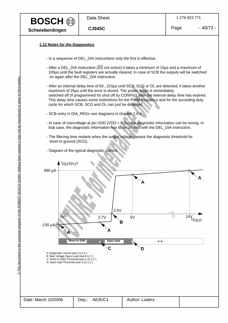
1.12 Notes for the Diagnostics
- In a sequence of DEL_DIA instructions only the first is effective.
- After a DEL_DIA instruction (SS not active) it takes a minimum of 15µs and a maximum of 100µs until the fault registers are actually cleared. In case of SCB the outputs will be switched on again after the DEL_DIA instruction.
- After an internal delay time of 60...215µs until SCB, SCG or OL are detected, it takes another maximum of 25µs until the error is stored. The power stage is immediately switched off (if programmed for shut off by CONFIG) after the internal delay time has expired. This delay time causes some restrictions for the PWM-frequency and for the according duty cycle for which SCB, SCG and OL can just be detected.
- SCB entry in DIA_REGx see diagrams in chapter 1.6.4.
- In case of overvoltage at pin VDD (VDD > 5,5V) the diagnostic information can be wrong. In that case, the diagnostic information has to be cleared with the DEL_DIA instruction.
- The filtering time restarts when the output voltage passes the diagnostic threshold for short to ground (SCG).
- Diagram of the typical diagnostic current:
A: Diagnostic current (see 3.11.3 )B: Bias Voltage Open Load (see3.11.2 )C: Short to GND Threshold (see 3.11.1.2 )D: Open load Threshold (see 3.11.1.1 )
IOUTPUT
2.7V 5V
-130 µA
580 µA
UOUT14V
A
A
B0V
A
A
Short to GND Open load o. k.
DC
3.5V
BOSCH©
Thi
s do
cum
ent i
s th
e ex
clus
ive
prop
erty
of t
he R
OB
ER
T B
OS
CH
Gm
bH. W
ithou
t the
ir co
nsen
t it m
ay n
ot b
e re
prod
uced
or g
iven
to th
ird p
artie
s. 1 279 923 771
Page - 41/72 -
Date: March 10/2006 Dep.: AE/EIC1 Author: Lüders
Data Sheet
CJ945C Schwieberdingen
OU
Tx o
n
Cur
rent
Con
trol
10 O
T
SC
G
SC
B
OTO
L
Fau
lt E
ntry
Deb
ounc
ing
Deb
ounc
ing
OT
SC
B
OL
SC
G
INx
LO
WO
UTx
of
f IN
x H
IGH
OU
Tx o
ff IN
x L
OW
T
oggl
ing
INx
HIG
H ->
LO
W
T
oggl
ing
INx
LO
W ->
HIG
H
SC
G
OL
OT
SC
B
To
gglin
g IN
x LO
W ->
HIG
H
No
Fau
lt N
o F
ault
No
Fau
lt
No
Act
ion
OL
OL
No
Deb
ounc
ing
00
CS
G F
ault
Ent
ry
SC
GS
CG
No
No
Act
ion
SC
B 10 S
CB
Fau
lt E
ntry
01 O
L F
ault
Ent
ryS
CB
No
10 S
CB
Fau
lt E
ntry
AB
C
Exe
mpl
ary
for a
pow
er s
tage
con
trolle
d by
inpu
t pin
INx.
Dia
gram
is a
ccor
ding
ly v
alid
for s
eria
l con
-tro
l via
SP
I or µ
sec-
bus.
The
SP
I ins
truct
ion
DE
L_D
IA d
elet
es a
ll fa
ult r
egis
ters
in a
ny s
tate
.O
n ac
tive
rese
t res
p. a
ctiv
e A
BE
(VD
D is
out
of r
ange
) out
put O
UTx
is s
witc
hed
off.
Afte
r res
et t
he
pow
er s
tage
is in
sta
te A
(exc
ept O
UT8
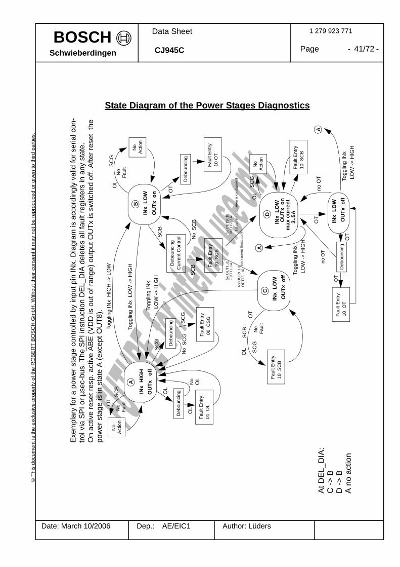
).State Diagram of the Power Stages Diagnostics
OU
Tx o
n IN
x L
OW
D
max
cur
rent
3..5
A
for O
UT1
..8,
OU
T11.
.14
for O
UT9
..10
OU
T15.
..16
A
To
gglin
g IN
x LO
W ->
HIG
H
10 S
CB
Fau
lt E
ntry
OU
Tx o
ff IN
x L
OW
OT
no O
TA
To
gglin
g IN
x LO
W ->
HIG
H
Deb
ounc
ing
no O
T
10 O
T F
ault
Ent
ryO
T
(if c
urre
nt li
mita
tion
is c
onfig
ured
)fo
r OU
T9..1
0O
UT1
5...1
6(n
o cu
rren
t lim
itatio
n)
Deb
ounc
ing
No
Act
ion
OL
SC
G
At D
EL_
DIA
:C
-> B
D ->
BA
no
actio
nO
T
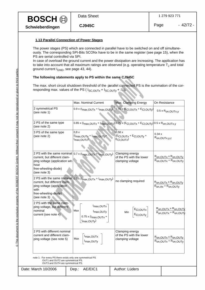
BOSCH©
Thi
s do
cum
ent i
s th
e ex
clus
ive
prop
erty
of t
he R
OB
ER
T B
OS
CH
Gm
bH. W
ithou
t the
ir co
nsen
t it m
ay n
ot b
e re
prod
uced
or g
iven
to th
ird p
artie
s. 1 279 923 771
Page - 42/72 -
Date: March 10/2006 Dep.: AE/EIC1 Author: Lüders
Data Sheet
CJ945C Schwieberdingen
1.13 Parallel Connection of Power Stages
The power stages (PS) which are connected in parallel have to be switched on and off simultane-ously. The corresponding SPI-Bits SCONx have to be in the same register (see page 15), when the PS are serial controlled via SPI.In case of overload the ground current and the power dissipation are increasing. The application has to take into account that all maximum ratings are observed (e.g. operating temperature TJ and total ground current IGND, see page 43, 44).
The following statements apply to PS within the same CJ945C
The max. short circuit shutdown threshold of the parallel connected PS is the summation of the cor-responding max. values of the PS ( ISC,OUTx + ISC,OUTy + ....).
note 1: For every PS there exists only one symmetrical PS OUT1 and OUT2 are symmetrical PS. OUT3 and OUT4 are symmetrical PS.
Max. Nominal Current Max. Clamping Energy On Resistance
2 symmetrical PS (see note 1)
0.9 x (Imax,OUTx + Imax,OUTy) 0.75 x (ECl,OUTx + ECl,OUTy)
2 PS of the same type(see note 2)
0.85 x (Imax,OUTx + Imax,OUTy) 0.75 x (ECl,OUTx + ECl,OUTy) 0.5 x Ron,OUTx,y
3 PS of the same type(see note 2)
0,8 x(Imax,OUTx + Imax,OUTy+ Imax,OUTz)
0,58 x(ECl,OUTx + ECl,OUTy + ECl,OUTz)
2 PS with the same nominal current, but different clam-ping voltage (application wit-hout free-wheeling-diode)(see note 3)
0.7 x (Imax,OUTx + Imax,OUTy) Clamping energy of the PS with the lower clamping voltage
2 PS with the same nominal current, but different clam-ping voltage (application with free-wheeling-diode)(see note 3)
0.7 x (Imax,OUTx + Imax,OUTy)no clamping required
2 PS with the same clam-ping voltage, but different nominal current (see note 4)
2 PS with different nominal current and different clam-ping voltage (see note 5)
Clamping energy of the PS with the lower clamping voltage
0.5 x Ron,OUTx,y
0.34 x Ron,OUTx,y,z
Ron,OUTx x Ron,OUTyRon,OUTx + Ron,OUTy
Ron,OUTx x Ron,OUTyRon,Ax + Ron,OUTy
Max
Imax,OUTx
Imax,OUTy
0.75 x (Imax,OUTx + Imax,OUTy)
ECl,OUTxECl,OUTy
MinRon,OUTx x Ron,OUTyRon,OUTx + Ron,OUTy
Imax,OUTxImax,OUTy
MaxRon,OUTx x Ron,OUTyRon,OUTx + Ron,OUTy

BOSCH©
Thi
s do
cum
ent i
s th
e ex
clus
ive
prop
erty
of t
he R
OB
ER
T B
OS
CH
Gm
bH. W
ithou
t the
ir co
nsen
t it m
ay n
ot b
e re
prod
uced
or g
iven
to th
ird p
artie
s. 1 279 923 771
Page - 43/72 -
Date: March 10/2006 Dep.: AE/EIC1 Author: Lüders
Data Sheet
CJ945C Schwieberdingen
... OUT17 and OUT18 are symmetrical PS.
note 2: PS of the same type have the same nominal current and the same clamping voltage
note 3: Parallel connection of PS-type 2,2A/45V with type 2,2A/70V
note 4: Parallel connection of PS-type 2,2A/45V with type 3.0A/45V or Parallel connection of PS-type 1.1A/45V with type 2,2A/45V note 5: Parallel connection of PS-type 2,2A/70V with type 1.1A/45V or Parallel connection of PS-type 2,2A/70V with type 3.0A/45V
If the power stages are configured for static current limitation the max. current limitation of the parallel connected PS is the summation of the corresponding max. values of thePS ( ISC,OUTx + ISC,OUTy + ....).
The following statements apply to Power Stages within different CJ945C
The application has to take into account that all maximum ratings of each CJ945C are observed.

BOSCH©
Thi
s do
cum
ent i
s th
e ex
clus
ive
prop
erty
of t
he R
OB
ER
T B
OS
CH
Gm
bH. W
ithou
t the
ir co
nsen
t it m
ay n
ot b
e re
prod
uced
or g
iven
to th
ird p
artie
s. 1 279 923 771
Page - 44/72 -
Date: March 10/2006 Dep.: AE/EIC1 Author: Lüders
Data Sheet
CJ945C Schwieberdingen
2. Maximum Ratings
2.1 Definition of Test Conditions
The integrated circuit must not be destroyed if maximum ratings are reached. Every maximum rating is allowed to reach, as far as no other maximum rating is exceeded.
Unless otherwise indicated all voltages are referred to GND (GND pins 1...8 connected to each other)
Positive current flows into the pin.
2.2 Test Coverage (TC) in Series Production
In the standard production flow not all parameters can be covered due to technical or economicreasons. Therefore the following test coverage was defined:
A) Parameter testB) Go/NoGo test (in the course of release qualification/characterization: parameter test)C) Guaranteed by design (covered by lab tests, not considered within the standard production flow)
2.3 Thermal Limits
Operating temperaturecontinuous -40°C ≤ TJ ≤ 150°Cfor 1000h accumulated 150°C ≤ TJ ≤ 175°C
Storage temperature -55°C ≤ TC ≤ 125°C
Thermal resistance RthJC ≤ 2,5 K/W
2.4 Electrical Limits
Limits must absolutely not be exceeded. By exceeding only one limit the integrated circuit might be destroyed.
Power Supplies UVDD and UUBatt
Static (without destruction) *) -0.3V ≤ UVDD ≤ 36V -1.0V ≤ UUBatt ≤ 37V
Dynamic <10 µsec (without destruction) -0.5V ≤ UVDD ≤ 36V -1.0V ≤ UUBatt ≤ 40V
*) UVDD > 5.5V is allowed only in case of error conditions! Not suitable for continuous operation.

BOSCH©
Thi
s do
cum
ent i
s th
e ex
clus
ive
prop
erty
of t
he R
OB
ER
T B
OS
CH
Gm
bH. W
ithou
t the
ir co
nsen
t it m
ay n
ot b
e re
prod
uced
or g
iven
to th
ird p
artie
s. 1 279 923 771
Page - 45/72 -
Date: March 10/2006 Dep.: AE/EIC1 Author: Lüders
Data Sheet
CJ945C Schwieberdingen
Outputs Low Side Switches
Static voltage (without destruction) OUT1...6 ≤ 64VOUT7..18 ≤ 40V
Dynamic voltage without destruction after ISO/DIS7637-1, pulses 1 to 4 OUT1 to 6, OUT9 to16: via external load (e.g. 2W lamp) ≤ 2ms OUT7, OUT8, OUT17 and OUT18: via external load ≤ 2ms
Ground Current
Total current GND1+2 (pins 26/27) IGND1+2 ≤ 18 A (total ground current of OUT5,6,9,10,17,18)
Total current GND3+4 (pins 58/59) IGND3+4 ≤ 20 A (total ground current of OUT1,2,7,8,11,12,15,16)
Total current GND5+6 (pins 11/12) IGND5+6 ≤ 6 A (total ground current of OUT3,13)
Total current GND7+8 (pins 41/42) IGND7+8 ≤ 6 A (total ground current of OUT4,14)
Attention: Even if all ground pins are connected with each other on the PCB the totalground currents IGND1+2 and IGND3+4 and IGND5+6 and IGND7+8 must not be exceeded.
The 4 ground pins GND1...4 are internally connected to the heat sink via an unspecifiedrivet joint. Therefore it is advisable to short-circuit the 4 ground pins on the PCB and to connect them with the heat sink. In addition the 4 ground pins GND5..8 must be connectedto the other ground pins on the PCB
Inputs of the Power Switches, SPI Inputs, Reset and Shut-off of the Power Stages
Input voltage -0.3V ≤ UINi,RST,SS,SI,SCK,ABE ≤ 36V
Input currents see 3.4.4 , 3.9.1 , 3.9.2 , 3.9.3 , 3.13.2
Pin RST
Minimum reset duration (Power-On) 15 ms
Input currents see 3.4.4
SPI Output
Output voltage -0.3V ≤ USO ≤ 36V
Output current ISO ≤ 5mA
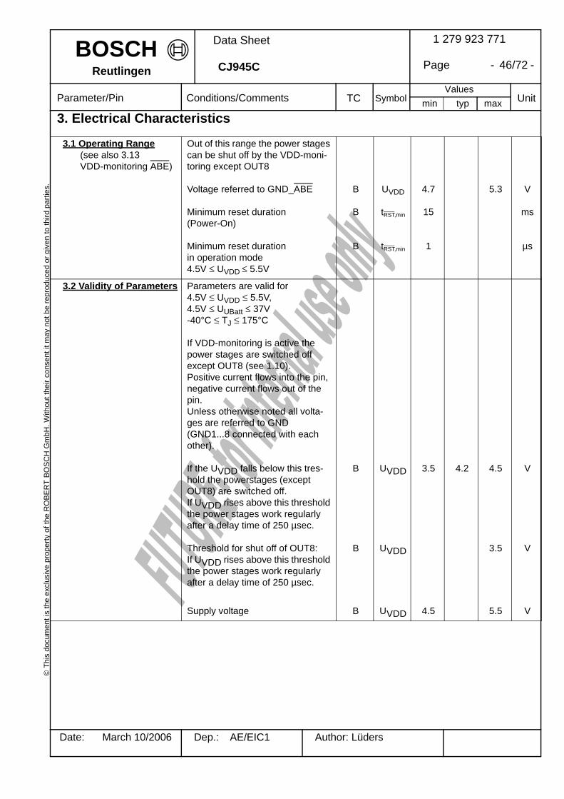
BOSCH©
Thi
s do
cum
ent i
s th
e ex
clus
ive
prop
erty
of t
he R
OB
ER
T BO
SC
H G
mbH
. With
out t
heir
cons
ent i
t may
not
be
repr
oduc
ed o
r giv
en to
third
par
ties.
typ maxminValues
Conditions/Comments
1 279 923 771
Page - 46/72 -
Date: March 10/2006 Dep.: AE/EIC1 Author: Lüders
Data Sheet
CJ945C
Parameter/Pin Symbol UnitTC
Reutlingen
3. Electrical Characteristics
3.1 Operating Range(see also 3.13 VDD-monitoring ABE)
Out of this range the power stages can be shut off by the VDD-moni-toring except OUT8
Voltage referred to GND_ABE
Minimum reset duration (Power-On)
Minimum reset duration in operation mode4.5V ≤ UVDD ≤ 5.5V
B
B
B
UVDD
tRST,min
tRST,min
4.7
15
1
5.3 V
ms
µs
3.2 Validity of Parameters Parameters are valid for 4.5V ≤ UVDD ≤ 5.5V,4.5V ≤ UUBatt ≤ 37V-40°C ≤ TJ ≤ 175°C
If VDD-monitoring is active the power stages are switched off except OUT8 (see 1.10).Positive current flows into the pin, negative current flows out of the pin.Unless otherwise noted all volta-ges are referred to GND (GND1...8 connected with each other).
If the UVDD falls below this tres-hold the powerstages (except OUT8) are switched off.If UVDD rises above this threshold the power stages work regularly after a delay time of 250 µsec.
Threshold for shut off of OUT8:If UVDD rises above this threshold the power stages work regularly after a delay time of 250 µsec.
B
B
UVDD
UVDD
3.5 4.2 4.5
3.5
V
V
Supply voltage B UVDD 4.5 5.5 V

BOSCH©
Thi
s do
cum
ent i
s th
e ex
clus
ive
prop
erty
of t
he R
OB
ER
T BO
SC
H G
mbH
. With
out t
heir
cons
ent i
t may
not
be
repr
oduc
ed o
r giv
en to
third
par
ties.
typ maxminValues
Conditions/Comments
1 279 923 771
Page - 47/72 -
Date: March 10/2006 Dep.: AE/EIC1 Author: Lüders
Data Sheet
CJ945C
Parameter/Pin Symbol UnitTC
Reutlingen
3.3 Power Consumption UVDD ≤ 5.5V 5.5V < UVDD < 36V (is not destroyed)UUBatt = 14V UUBatt = 28V UUBatt ≤ UVDD Power consumption in standby mode in case of missing UVDD,UUBatt ≤ 14V
AAAAA
A
IVDDIVDDIUBattIUBattIUBatt
IUBatt
2050341
200
mAmAmAmAmA
µA
3.4 Inputs of the Power Stages and ResetIN1...IN16, RST
Outputs are switched off if inputs are open (parallel control).
3.4.1 Low Level Reset not active,Power stage on fori = 1...7, 9...16
Power stage off fori = 8
B
B
B
URSTL
UINiL
UINiL
1.0
1.0
1.0
V
V
V
3.4.2 High Level Power stage off for i = 1...7, 9...16
Power stage on fori = 8, UVDD = 4.0Vi = 8, UVDD = 5.0V
BB
BB
URSTHUINiH
UINiHUINiH
2.02.0
2.102.30
VV
VV
3.4.3 Hysteresis C ∆UINi,∆URST
0.1 0.6 V

BOSCH©
Thi
s do
cum
ent i
s th
e ex
clus
ive
prop
erty
of t
he R
OB
ER
T BO
SC
H G
mbH
. With
out t
heir
cons
ent i
t may
not
be
repr
oduc
ed o
r giv
en to
third
par
ties.
typ maxminValues
Conditions/Comments
1 279 923 771
Page - 48/72 -
Date: March 10/2006 Dep.: AE/EIC1 Author: Lüders
Data Sheet
CJ945C
Parameter/Pin Symbol UnitTC
Reutlingen
3.4.4 Input CurrentsINi, RST
-0.3V ≤ UINi,RST ≤ UVDD(i = 1...5, 9...15)
-0.3V ≤ UINi ≤ UVDD(i = 6,7,16)
-0.3V ≤ UIN8 ≤ UVDD
0.8V ≤ UIN8 ≤ 36V , pull down
0V ≤ URST ≤ UVDD - 1.5V, pull up
0V ≤ UINi ≤ UVDD - 1.5V, pull up(i = 6,7,16)
Bit BMUX = 1 (CONFIG_REG):0V ≤ UINi ≤ UVDD - 1.5V, pull up(i = 1..5, 9..15)
Bit BMUX = 0 (CONFIG_REG):0V ≤ UINi ≤ UVDD, high-impedance(i = 1..5, 9..15)
UVDD ≤ UINi ≤ 36V(i = 1..7, 9..16)
A/B
A/B
A/B
A
A
A
A
A
A
IINi,RST
IINi
IIN8
IIN8
-IRST
-IINi
-IINi
|IINi|
|IINi|
-100
-20
-50
20
20
5
20
35
40
10
40
5
5
50
50
100
20
100
1
5
µA
µA
µA
µA
µA
µA
µA
µA
µA
3.4.5 Input Protection INi Input clamping at INi (i = 1...16):No malfunction during clamping,if the pins INx are not floating.Max. clamping current (externallylimited)staticdynamic (t < 2ms)
Max. clamping voltage IINi = -5mAIINi = +5mA
External current limitation at INi is only provided if µsec-bus control is used. In that case INi are used as digital inputs. If µsec-bus is not used, there is no external resistor for current limitation. See 2.4 “Inputs of the Power Switches, SPI Inputs...”
CC
CC
|IINi||IINi|
UINiUINi
-1.537
25
65
mAmA
VV
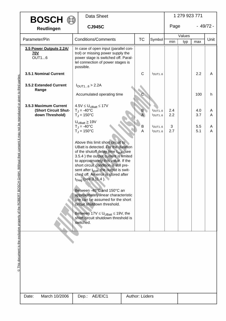
BOSCH©
Thi
s do
cum
ent i
s th
e ex
clus
ive
prop
erty
of t
he R
OB
ER
T BO
SC
H G
mbH
. With
out t
heir
cons
ent i
t may
not
be
repr
oduc
ed o
r giv
en to
third
par
ties.
typ maxminValues
Conditions/Comments
1 279 923 771
Page - 49/72 -
Date: March 10/2006 Dep.: AE/EIC1 Author: Lüders
Data Sheet
CJ945C
Parameter/Pin Symbol UnitTC
Reutlingen
3.5 Power Outputs 2.2A/70VOUT1...6
In case of open input (parallel con-trol) or missing power supply the power stage is switched off. Paral-lel connection of power stages is possible.
3.5.1 Nominal Current C IOUT1..6 2.2 A
3.5.2 Extended Current Range
IOUT1...6 > 2.2A
Accumulated operating time C 100 h
3.5.3 Maximum Current (Short Circuit Shut- down Threshold)
4.5V ≤ UUBatt ≤ 17VTJ = -40°C TJ = 150°C
BA
IOUT1..6IOUT1..6
2.42.2
4.03.7
AA
UUBatt > 19VTJ = -40°C TJ = 150°C
BA
IOUT1..6IOUT1..6
32.7
5.55.1
AA
Above this limit short circuit to UBatt is detected. For the duration of the shutoff delay time tVoff (see 3.5.4 ) the output current is limited to approximately this value. If the short circuit condition is still pre-sent after tVoff, the output is swit-ched off. An error is stored after tDiag (see 3.11.4 ).
Between -40°C and 150°C an approximately linear characteristic line can be assumed for the short circuit shutdown threshold.
Between 17V ≤ UUBatt ≤ 19V, the short circuit shutdown threshold is switched.

BOSCH©
Thi
s do
cum
ent i
s th
e ex
clus
ive
prop
erty
of t
he R
OB
ER
T BO
SC
H G
mbH
. With
out t
heir
cons
ent i
t may
not
be
repr
oduc
ed o
r giv
en to
third
par
ties.
typ maxminValues
Conditions/Comments
1 279 923 771
Page - 50/72 -
Date: March 10/2006 Dep.: AE/EIC1 Author: Lüders
Data Sheet
CJ945C
Parameter/Pin Symbol UnitTC
Reutlingen
3.5.3.1 Maximum Battery Voltage at Short Cir- cuit to Battery
A power stage that is switched off in case of SCB can be switched on again by an off/on cycle at the cor-responding input pin resp. by the change of the state of the corre-sponding SPI bit SCONx (see 1.6.1), by the µsec-Bus, by a DEL_DIA instruction or can be released again by reset. If the fault register is cleared before this release (by a DEL_DIA instruc-tion), a new fault entry of SCB is immediately carried out, even if SCB condition is no longer pre-sent.
See Note 1.11.1 C UOUT 1..6
36 V
3.5.4 Shutoff Delay Shutoff delay of the power stages after detection of SCB
B tVoff 60 215 µs
3.5.5 On Resistance TJ = 25°CTJ = 150°C TJ = -40°CTJ = 175°CFor UUBatt ≤ 10V Ron is increased up to 20%.
AAAC
Ron1...6Ron1...6Ron1...6Ron1...6
150300100300
260480200500
400720350800
mΩmΩmΩmΩ
3.5.6 On/off Delay Times „On“
„Off“(measured with ohmic load)|tdon - tdoff|
BBBBC
tdon1...6tson1...6tdoff1...6tsoff1...6
∆td
105
10105
µsµsµsµsµs
switch-on slew rateswitch-off slew rate
CC
son1...6soff1...6
1521
V/µsV/µs
3.5.7 Leakage Current UVDD = 0V, UOUT1...6 = 14V (lea-kage current of the DMOS, dia-gnostic current = 0)
UVDD = 0V, UOUT1...6 = 24V (lea-kage current of the DMOS, dia-gnostic current = 0)
A
A
IOUT1..6
IOUT1..6
10
20
µA
µA
3.5.8 Clamping
3.5.8.1 Clamping Voltage IOUT1...6 = 0.1A A UOUT1..6 64 78 V

BOSCH©
Thi
s do
cum
ent i
s th
e ex
clus
ive
prop
erty
of t
he R
OB
ER
T BO
SC
H G
mbH
. With
out t
heir
cons
ent i
t may
not
be
repr
oduc
ed o
r giv
en to
third
par
ties.
typ maxminValues
Conditions/Comments
1 279 923 771
Page - 51/72 -
Date: March 10/2006 Dep.: AE/EIC1 Author: Lüders
Data Sheet
CJ945C
Parameter/Pin Symbol UnitTC
Reutlingen
3.5.8.2 Matching of the Clamping Voltage
Between different outputs with identical inductive loads
A ∆U 3 V
3.5.8.3 Maximum Clamping EnergyTC ≤ 110°C
Linear decreasing current, fmax = 50Hz (see diagrams E = f(I) on 3.14)
IOUT1...6 ≤ 2.2A C E 8.5 mJ
IOUT1...6 ≤ 1.0A C E 19 mJ
IOUT1...6 ≤ 0.5A C E 30 mJ
3.5.8.4 Maximum Clamping EnergyTC ≤ 60°C
Linear decreasing current, fmax = 50Hz
IOUT1...6 ≤ 2.2A C E 10.8 mJ
IOUT1...6 ≤ 1.0A C E 22 mJ
IOUT1...6 ≤ 0.5A C E 36 mJ
3.5.8.5 Maximum Clamping Energy with two Outputs connected in parallel
Each output 75% of the values of 3.5.8.3 resp. 3.5.8.4
C
3.5.8.6 Maximum Clamping Energy at Load Dump
For a maximum of 10 times during ECU life (load dump with 400ms and Ri = 2Ω over the load, e.g. 2W lamp)
C E 50 mJ
3.5.8.7 Jump Start Each output 150% of the values of 3.5.8.4 .For a maximum of 10 jump starts of 2 minutes each during ECU life.
C
3.5.8.8 Single pulse TC ≤ 60°C
IOUT1...6 ≤ 0.6A , max 10 000 pulse C E 50 mJ
3.6 Power outputs 2.2A/45VOUT9...OUT14
In case of open input (parallel con-trol) or missing power supply the power stage is switched off. Paral-lel connection of power stages is possible.
3.6.1 Nominal Current C IOUT9...14
2.2 A
3.6.2 Extended Current Range
IOUTi > 2.2A
Accumulated operating time C 100 h
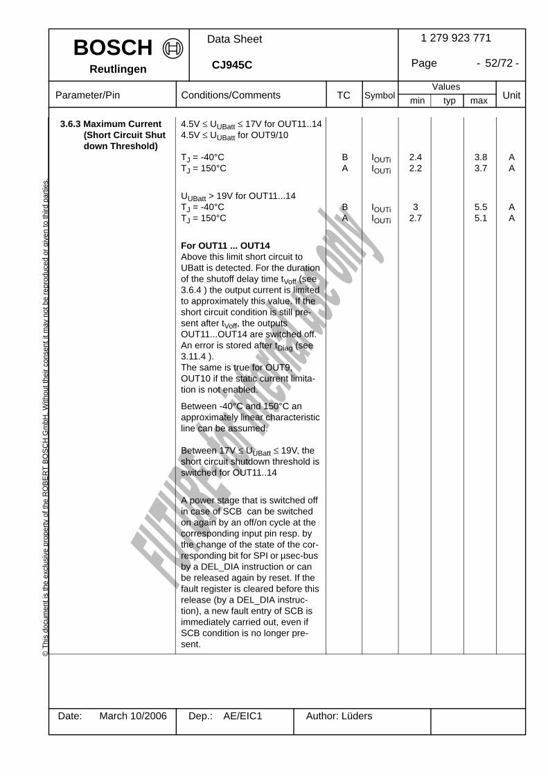
BOSCH©
Thi
s do
cum
ent i
s th
e ex
clus
ive
prop
erty
of t
he R
OB
ER
T BO
SC
H G
mbH
. With
out t
heir
cons
ent i
t may
not
be
repr
oduc
ed o
r giv
en to
third
par
ties.
typ maxminValues
Conditions/Comments
1 279 923 771
Page - 52/72 -
Date: March 10/2006 Dep.: AE/EIC1 Author: Lüders
Data Sheet
CJ945C
Parameter/Pin Symbol UnitTC
Reutlingen
3.6.3 Maximum Current (Short Circuit Shut down Threshold)
4.5V ≤ UUBatt ≤ 17V for OUT11..144.5V ≤ UUBatt for OUT9/10
TJ = -40°CTJ = 150°C
BA
IOUTiIOUTi
2.42.2
3.83.7
AA
UUBatt > 19V for OUT11...14 TJ = -40°CTJ = 150°C
BA
IOUTiIOUTi
32.7
5.55.1
AA
For OUT11 ... OUT14Above this limit short circuit to UBatt is detected. For the duration of the shutoff delay time tVoff (see 3.6.4 ) the output current is limited to approximately this value. If the short circuit condition is still pre-sent after tVoff, the outputs OUT11...OUT14 are switched off. An error is stored after tDiag (see 3.11.4 ).The same is true for OUT9, OUT10 if the static current limita-tion is not enabled.
Between -40°C and 150°C an approximately linear characteristic line can be assumed.
Between 17V ≤ UUBatt ≤ 19V, the short circuit shutdown threshold is switched for OUT11..14
A power stage that is switched off in case of SCB can be switched on again by an off/on cycle at the corresponding input pin resp. by the change of the state of the cor-responding bit for SPI or µsec-bus by a DEL_DIA instruction or can be released again by reset. If the fault register is cleared before this release (by a DEL_DIA instruc-tion), a new fault entry of SCB is immediately carried out, even if SCB condition is no longer pre-sent.

BOSCH©
Thi
s do
cum
ent i
s th
e ex
clus
ive
prop
erty
of t
he R
OB
ER
T BO
SC
H G
mbH
. With
out t
heir
cons
ent i
t may
not
be
repr
oduc
ed o
r giv
en to
third
par
ties.
typ maxminValues
Conditions/Comments
1 279 923 771
Page - 53/72 -
Date: March 10/2006 Dep.: AE/EIC1 Author: Lüders
Data Sheet
CJ945C
Parameter/Pin Symbol UnitTC
Reutlingen
For OUT9, OUT10Above this limit short circuit to UBatt is detected. The output cur-rent is limited to approximately this value if the static current limitation is configured. An error is stored after tDiag (see 3.11.4 ). If the ope-ration leads to an overtemperature condition, a second protection level (about 170°C) will change the output into a low duty cycle PWM (selctive thermal shutdown with restart) to prevent critical chip tem-peratures
3.6.3.1 Maximum Battery Voltage at Short Cir- cuit to Battery
Between -40°C and 150°C an approximately linear characteristic line can be assumed.
See Note 1.11.1
For OUT11 ... 14
For OUT9 , OUT10without static current limitationwith configured static current limi-tation
C
CC
UOUT11..14
UOUT 9..10
36
3624
V
VV
3.6.4 Shutoff Delay Shutoff delay of the power stages after detection of KSUB. For the duration of tVoff current is limited to maximum current.
B tVoff 60 215 µs
3.6.5 On Resistance OUT9...14:TJ = 25°COUT9...14:TJ = 150°COUT9...14:TJ = -40°COUT9...14:TJ = 175°C
AAAC
RonRonRonRon
150300100300
300500200500
380650300750
mΩmΩmΩmΩ
For UUBatt ≤ 10V Ron is increased up to 20%.
3.6.6 On /off Delay Times „On“
„Off“ (measurement with ohmic load)|tdon - tdoff|
BBBBC
tdontsontdofftsoff∆td
105
10105
µsµsµsµsµs
switch-on slew rateswitch-off slew rate
CC
sonsoff
2025
V/µsV/µs

BOSCH©
Thi
s do
cum
ent i
s th
e ex
clus
ive
prop
erty
of t
he R
OB
ER
T BO
SC
H G
mbH
. With
out t
heir
cons
ent i
t may
not
be
repr
oduc
ed o
r giv
en to
third
par
ties.
typ maxminValues
Conditions/Comments
1 279 923 771
Page - 54/72 -
Date: March 10/2006 Dep.: AE/EIC1 Author: Lüders
Data Sheet
CJ945C
Parameter/Pin Symbol UnitTC
Reutlingen
3.6.7 Leakage Current UVDD = 0V, UOUT9...14 = 14V (leakage current of the DMOS, diagnostic current = 0)
UVDD = 0V, UOUT9...14 = 24V (leakage current of the DMOS, diagnostic current = 0)
A
A
IOUTi
IOUTi
10
20
µA
µA
3.6.8 Clamping
3.6.8.1 Clamping Voltage IOUTi = 0.2A A U9...14 40 45 50 V
3.6.8.2 Maximum Clamping EnergyTC ≤ 110°C
Linear decreasing current, fmax = 30Hz (see diagrams E = f(I) on 3.14)
IOUT9...14 ≤ 2.2A C E 14 mJ
IOUT9...14 ≤ 1.0A C E 30 mJ
3.6.8.3 Maximum Clamping EnergyTC ≤ 60°C
Linear decreasing current, fmax = 30Hz
IOUT9...14 ≤ 2.2A C E 17 mJ
IOUT9...14 ≤ 1.0A C E 36 mJ
3.6.8.4 Maximum Clamping Energy with two Outputs connected in parallel
Each output 75% of the values of 3.6.8.2 resp. 3.6.8.3 .
C
3.6.8.5 Maximum Clamping Energy at Load Dump
For a maximum of 10 times during ECU life (load dump with 400ms and Ri = 2Ω over the load, e.g. 2W lamp)
C E 50 mJ
3.6.8.6 Jump Start Each output 150% of the values of 3.6.8.3 . For a maximum of 10 jump starts of 2 minutes each during ECU life.
C
3.6.8.7 Single pulse TC ≤ 60°C
IOUT9...14 ≤ 0.6A , max 10 000 pulse
C E 50 mJ
3.7 Power outputs 3.0A/45VOUT15...OUT16
In case of open input (parallel con-trol) or missing power supply the power stage is switched off. Paral-lel connection of power stages is possible.
3.7.1 Nominal Current C IOUT15IOUT16
3.0 A

BOSCH©
Thi
s do
cum
ent i
s th
e ex
clus
ive
prop
erty
of t
he R
OB
ER
T BO
SC
H G
mbH
. With
out t
heir
cons
ent i
t may
not
be
repr
oduc
ed o
r giv
en to
third
par
ties.
typ maxminValues
Conditions/Comments
1 279 923 771
Page - 55/72 -
Date: March 10/2006 Dep.: AE/EIC1 Author: Lüders
Data Sheet
CJ945C
Parameter/Pin Symbol UnitTC
Reutlingen
3.7.2 Extended Current Range
IOUT15,16 > 3.0A
Accumulated operating time C 100 h
3.7.3 Maximum Current (Short Circuit Shut down threshold)
UUBatt > 4.5VTJ = -40°CTJ = 150°C
Above this limit short circuit to UBatt is detected. For the duration of the shutoff delay time tVoff (see 3.6.4 ) the output current is limited to approximately this value. If the short circuit condition is still pre-sent after tVoff, the outputs OUT15/16 are switched off if the static cur-rent limitation is not enabled. An error is stored after tDiag (see 3.11.4 ).
BA
IOUT15IOUT16
3.33
65.5
AA
Above this limit short circuit to UBatt is detected. The output cur-rent is limited to approximately this value if the static current limitation is configured. An error is stored after tDiag (see 3.11.4 ). If the ope-ration leads to an overtemperature condition, a second protection level (about 170°C) will change the output into a low duty cycle PWM (selctive thermal shutdown with restart) to prevent critical chip tem-peratures.
3.7.3.1 Maximum Battery Voltage at Short Cir- cuit to Battery
Between -40°C and 150°C an approximately linear characteristic line can be assumed.
See Note 1.11.1
without static current limitationwith configured static current limi-tation
CC
UOUT 15, 16
3624
VV
3.7.4 Shuttoff Delay Shutoff delay of the power stages after detection of SCB. For the duration of tVoff current is limited to maximum current.
B tVoff 60 215 µs
3.7.5 On Resistance TJ = 25°C:TJ = 150°C:TJ = -40°C:TJ = 175°C:
AAAC
RonRonRonRon
10012050120
200350150350
280470250550
mΩmΩmΩmΩ
BOSCH©
Thi
s do
cum
ent i
s th
e ex
clus
ive
prop
erty
of t
he R
OB
ER
T BO
SC
H G
mbH
. With
out t
heir
cons
ent i
t may
not
be
repr
oduc
ed o
r giv
en to
third
par
ties.
typ maxminValues
Conditions/Comments
1 279 923 771
Page - 56/72 -
Date: March 10/2006 Dep.: AE/EIC1 Author: Lüders
Data Sheet
CJ945C
Parameter/Pin Symbol UnitTC
Reutlingen
For UUBatt ≤ 10V Ron is increased up to 20%.
3.7.6 On /off Delay Times „On“ „Off“ (measurement with ohmic load)|tdon - tdoff|
BBBBC
tdontsontdofftsoff∆td
105
10105
µsµsµsµsµs
switch-on slew rateswitch-off slew rate
CC
sonsoff
2025
V/µsV/µs
3.7.7 Leakage Current UVDD = 0V, UOUT15,16 = 14V (leakage current of the DMOS, diagnostic current = 0)
UVDD = 0V, UOUT15,16 = 24V (leakage current of the DMOS, diagnostic current = 0)
A
A
IOUT15,16
IOUT15,16
10
20
µA
µA
3.7.8 Clamping
3.7.8.1 Clamping Voltage IOUT15,16 = 0.2A UOUT15,
16
40 45 50 V
3.7.8.2 Maximum Clamping EnergyTC ≤ 110°C
Linear decreasing current, fmax = 30Hz (see diagrams E = f(I) on 3.14)
IOUT15,16 ≤ 3.0A C E 18 mJ
IOUT15,16 ≤ 2.2A C E 20 mJ
IOUT15,16 ≤ 1.5A C E 24 mJ
IOUT15,16 ≤ 1.0A C E 40 mJ
3.7.8.3 Maximum Clamping EnergyTC ≤ 60°C
Linear decreasing current, fmax = 30Hz
IOUT15,16 ≤ 3.0A C E 20 mJ
IOUT15,16 ≤ 1.0A C E 46 mJ
3.7.8.4 Maximum Clamping Energy with two Outputs connected in parallel
Each output 75% of the values of 3.7.8.2 resp. 3.7.8.3 .
C
3.7.8.5 Maximum Clamping Energy at Load Dump
For a maximum of 10 times during ECU life (load dump with 400ms and Ri = 2Ω over the load, e.g. 2W lamp)
C E 50 mJ

BOSCH©
Thi
s do
cum
ent i
s th
e ex
clus
ive
prop
erty
of t
he R
OB
ER
T BO
SC
H G
mbH
. With
out t
heir
cons
ent i
t may
not
be
repr
oduc
ed o
r giv
en to
third
par
ties.
typ maxminValues
Conditions/Comments
1 279 923 771
Page - 57/72 -
Date: March 10/2006 Dep.: AE/EIC1 Author: Lüders
Data Sheet
CJ945C
Parameter/Pin Symbol UnitTC
Reutlingen
3.7.8.6 Jump Start Each output 150% of the values of 3.7.8.3 . For a maximum of 10 jump starts of 2 minutes each during ECU life.
C
3.7.8.7 Single pulse TC ≤ 60°C
IOUT15, 16 ≤ 0.6A , max 10 000 pul-ses
C E 50 mJ
3.8 Power Outputs 1.1A/45VOUT7,8, OUT17,18
In case of open input (parallel con-trol) or missing power supply the power stage is switched off. Paral-lel connection of power stages is possible.
3.8.1 Nominal Current for OUT7, 8, 17, 18 C IOUTi 1.1 A
3.8.2 Extended Current Range
IOUT7,8,17,18 > 1.1A
Accumulated operating time C 100 h
3.8.3 Maximum Current (Short Circuit Shut down Threshold and static current limitation)
4.5V ≤ UUBatt ≤ 17V for OUT7, 84.5V ≤ UUBatt for OUT17,18
TJ = -40°CTJ = 150°C
BA
IOUTiIOUTi
1.21.1
2.22.0
AA
UUBatt > 19V only for OUT7,8TJ = -40°CTJ = 150°C
BA
IOUTiIOUTi
1.51.3
2.52.3
AA
For OUT7, OUT8Above this limit short circuit to UBatt is detected. For the duration of the shutoff delay time tVoff (see 3.8.4 ) the output current is limited to approximately this value. If the short circuit condition is still pre-sent after tVoff, the outputs OUT7/8 are switched off. An error is stored after tDiag (see 3.11.4 ).The same is true for OUT17 OUT18 if the static current limita-tion is not enabled.
Between -40°C and 150°C an approximately linear characteristic line can be assumed.
Between 17V ≤ UUBatt ≤ 19V, the short circuit shutdown threshold is switched for OUT7/8

BOSCH©
Thi
s do
cum
ent i
s th
e ex
clus
ive
prop
erty
of t
he R
OB
ER
T BO
SC
H G
mbH
. With
out t
heir
cons
ent i
t may
not
be
repr
oduc
ed o
r giv
en to
third
par
ties.
typ maxminValues
Conditions/Comments
1 279 923 771
Page - 58/72 -
Date: March 10/2006 Dep.: AE/EIC1 Author: Lüders
Data Sheet
CJ945C
Parameter/Pin Symbol UnitTC
Reutlingen
A power stage that is switched off in case of SCB can be switched on again by an off/on cycle at the corresponding input pin resp. by the change of the state of the cor-responding bit for SPI or µsec-bus by a DEL_DIA instruction or can be released again by reset. If the fault register is cleared before this release (by a DEL_DIA instruc-tion), a new fault entry of SCB is immediately carried out, even if SCB condition is no longer pre-sent.
For OUT17, OUT18Above this limit short circuit to UBatt is detected. The output cur-rent is limited to approximately this value if the static current limitation is configured. An error is stored after tDiag (see 3.11.4 ). If the ope-ration leads to an overtemperature condition, a second protection level (about 170°C) will change the output into a low duty cycle PWM (selctive thermal shutdown with restart) to prevent critical chip tem-peratures
3.8.3.1 Maximum Battery Voltage at Short Cir- cuit to Battery
Between -40°C and 150°C an approximately linear characteristic line can be assumed.
See Note 1.11.1
For OUT7, OUT8
For OUT17 , OUT18without static current limitationwith configured static current limi-tation
C
CC
UOUT 7, 8
UOUT 17, 18
36
3624
V
VV
3.8.4 Shutoff Delay Shutoff delay of the power stages after detection of SCB. For the duration of tVoff current is limited to maximum current.
B tVoff 60 215 µs
BOSCH©
Thi
s do
cum
ent i
s th
e ex
clus
ive
prop
erty
of t
he R
OB
ER
T BO
SC
H G
mbH
. With
out t
heir
cons
ent i
t may
not
be
repr
oduc
ed o
r giv
en to
third
par
ties.
typ maxminValues
Conditions/Comments
1 279 923 771
Page - 59/72 -
Date: March 10/2006 Dep.: AE/EIC1 Author: Lüders
Data Sheet
CJ945C
Parameter/Pin Symbol UnitTC
Reutlingen
3.8.5 On Resistance For OUT7,8, OUT17,18:TJ = 25°CTJ = 150°CTJ = -40°CTJ = 175°CFor UUBatt ≤ 10V Ron is increased up to 20%.condition: UVDD > 4.5V
For OUT8 only:3.5V<(UVDD, UUBatt)<4,5VTJ = 25°CTJ = 150°CTJ = -40°CTJ = 175°C
AAAC
AAAC
RonRonRonRon
RonRonRonRon
250500150500
400750300800
78015006001500
100015009001500
mΩmΩmΩmΩ
mΩmΩmΩmΩ
3.8.6 On/off Delay Times „On“
„Off“ (measurement with ohmic load)|tdon - tdoff|
BBBBC
tdontsontdofftsoff∆td
105
10105
µsµsµsµsµs
Switch-on slew rateSwitch-off slew rate
CC
sonsoff
2540
V/µsV/µs
3.8.7 Leakage Current For OUT7,8, OUT1718:
UVDD = 0V, UOUTi = 14V (leakage current of the DMOS, diagnostic current = 0)
UVDD = 0V, UOUTi = 24V (leakage current of the DMOS, diagnostic current = 0)
A
A
IOUTi
IOUTi
10
20
µA
µA
3.8.8 Clamping For OUT7,8, OUT17,18:
3.8.8.1 Clamping Voltage IOUTi = 0.2A A UOUTi 40 45 50 V
3.8.8.2 Maximum Clamping EnergyTC ≤ 110°C
Linear decreasing current, fmax = 10Hz (see diagrams E = f(I) on 3.14)
IOUTi ≤ 0.6A IOUTi ≤ 1.1A
CC
EE
107
mJmJ
BOSCH©
Thi
s do
cum
ent i
s th
e ex
clus
ive
prop
erty
of t
he R
OB
ER
T BO
SC
H G
mbH
. With
out t
heir
cons
ent i
t may
not
be
repr
oduc
ed o
r giv
en to
third
par
ties.
typ maxminValues
Conditions/Comments
1 279 923 771
Page - 60/72 -
Date: March 10/2006 Dep.: AE/EIC1 Author: Lüders
Data Sheet
CJ945C
Parameter/Pin Symbol UnitTC
Reutlingen
3.8.8.3 Maximum Clamping EnergyTC ≤ 60°C
Linear decreasing current, fmax = 10Hz
IOUTi ≤ 0.6IOUTi ≤ 1.1A
CC
EE
128.5
mJmJ
3.8.8.4 Maximum Clamping Energy with two Outputs connected in parallel
Each output 75% of the values of 3.8.8.2 resp. 3.8.8.3 .
C
3.8.8.5 Maximum Clamping Energy at Load Dump
For a maximum of 10 times during ECU life (load dump with 400ms and Ri = 2Ω over the load)
C E 15 mJ
3.8.8.6 Jump Start Each output 150% of the values of 3.8.8.3 . For a maximum of 10 jump starts of 2 minutes each during ECU life
C
Note:Over lifetime (2000h/175) there is an increase of 10% of the maximum shortcircuit shut down threshold possible (see 3.5.3, 3.6.3, 3.7.3, 3.8.3)
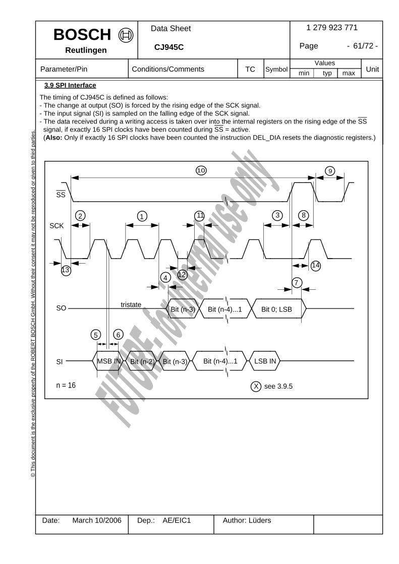
BOSCH©
Thi
s do
cum
ent i
s th
e ex
clus
ive
prop
erty
of t
he R
OB
ER
T BO
SC
H G
mbH
. With
out t
heir
cons
ent i
t may
not
be
repr
oduc
ed o
r giv
en to
third
par
ties.
typ maxminValues
Conditions/Comments
1 279 923 771
Page - 61/72 -
Date: March 10/2006 Dep.: AE/EIC1 Author: Lüders
Data Sheet
CJ945C
Parameter/Pin Symbol UnitTC
Reutlingen
3.9 SPI Interface
The timing of CJ945C is defined as follows:- The change at output (SO) is forced by the rising edge of the SCK signal.- The input signal (SI) is sampled on the falling edge of the SCK signal.- The data received during a writing access is taken over into the internal registers on the rising edge of the SS signal, if exactly 16 SPI clocks have been counted during SS = active. (Also: Only if exactly 16 SPI clocks have been counted the instruction DEL_DIA resets the diagnostic registers.)
SO
SI MSB IN Bit (n-4)...1 LSB IN
Bit (n-4)...1
1
4
5 6
SCK
SS
7
8
n = 16
910
32
Bit (n-3) Bit 0; LSBtristate
Bit (n-3)Bit (n-2)
11
12
X see 3.9.5
1413

BOSCH©
Thi
s do
cum
ent i
s th
e ex
clus
ive
prop
erty
of t
he R
OB
ER
T BO
SC
H G
mbH
. With
out t
heir
cons
ent i
t may
not
be
repr
oduc
ed o
r giv
en to
third
par
ties.
typ maxminValues
Conditions/Comments
1 279 923 771
Page - 62/72 -
Date: March 10/2006 Dep.: AE/EIC1 Author: Lüders
Data Sheet
CJ945C
Parameter/Pin Symbol UnitTC
Reutlingen
3.9.1 Input SCK SPI clock input
3.9.1.1 Low Level B USCKL 1.0 V
3.9.1.2 High Level B USCKH 2.0 V
3.9.1.3 Hysteresis C ∆USCK 0.1 0.6 V
3.9.1.4 Input Capacity C CSCK 10 pF
3.9.1.5 Input Current Pull up current source connected to VDD
A -ISCK 10 20 50 µA
3.9.2 Input SS Slave select signal
3.9.2.1 Low Level CJ945C is selected B USSL 1.0 V
3.9.2.2 High Level B USSH 2.0 V
3.9.2.3 Hysteresis C ∆USS 0.1 0.6 V
3.9.2.4 Input Capacity C CSS 10 pF
3.9.2.5 Input Current Pull up current source connected to VDD
A -ISS 10 20 50 µA
3.9.3 Input SI SPI data input
3.9.3.1 Low Level B USIL 1.0 V
3.9.3.2 High Level B USIH 2.0 V
3.9.3.3 Hysteresis C ∆USI 0.1 0.6 V
3.9.3.4 Input Capacity C CSI 10 pF
3.9.3.5 Input Current Pull up current source connected to VDD
A -ISI 10 20 50 µA
3.9.4 Output SO Tristate output of the CJ945C (SPI output);On active reset (RST) output SO is in tristate.
3.9.4.1 Low Level ISO = 2mA A USOL 0.4 V
3.9.4.2 High Level ISO = -2mA A USOH UVDD- 1.0
V
3.9.4.3 Capacity Capacity of the pin in tristate C CSO 10 pF
3.9.4.4 Leakage Current In tristate A ISO -10 10 µA
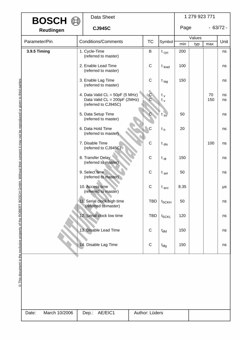
BOSCH©
Thi
s do
cum
ent i
s th
e ex
clus
ive
prop
erty
of t
he R
OB
ER
T BO
SC
H G
mbH
. With
out t
heir
cons
ent i
t may
not
be
repr
oduc
ed o
r giv
en to
third
par
ties.
typ maxminValues
Conditions/Comments
1 279 923 771
Page - 63/72 -
Date: March 10/2006 Dep.: AE/EIC1 Author: Lüders
Data Sheet
CJ945C
Parameter/Pin Symbol UnitTC
Reutlingen
3.9.5 Timing 1. Cycle-Time (referred to master)
2. Enable Lead Time (referred to master)
3. Enable Lag Time (referred to master)
4. Data Valid CL = 50pF (5 MHz) Data Valid CL = 200pF (2MHz) (referred to CJ945C)
5. Data Setup Time (referred to master)
6. Data Hold Time (referred to master)
7. Disable Time (referred to CJ945C)
8. Transfer Delay (referred to master)
9. Select time (referred to master)
10. Access time (referred to master)
11. Serial clock high time (referred to master)
12. Serial clock low time
13. Disable Lead Time
14. Disable Lag Time
B
C
C
CC
C
C
C
C
C
C
TBD
TBD
C
C
t cyc
t lead
t lag
t vt v
t su
t h
t dis
t dt
t sel
t acc
tSCKH
tSCKL
tdld
tdlg
200
100
150
50
20
150
50
8.35
50
120
150
150
70150
100
ns
ns
ns
nsns
ns
ns
ns
ns
ns
µs
ns
ns
ns
ns

BOSCH©
Thi
s do
cum
ent i
s th
e ex
clus
ive
prop
erty
of t
he R
OB
ER
T BO
SC
H G
mbH
. With
out t
heir
cons
ent i
t may
not
be
repr
oduc
ed o
r giv
en to
third
par
ties.
typ maxminValues
Conditions/Comments
1 279 923 771
Page - 64/72 -
Date: March 10/2006 Dep.: AE/EIC1 Author: Lüders
Data Sheet
CJ945C
Parameter/Pin Symbol UnitTC
Reutlingen
3.10 µsec-bus
Notes for the timing:
A rising edge at SSY and a falling edge at FCL must not occur simultaneously!On the rising edge of SSY the 16 bits clocked in CJ945C by the last 16 falling edges at FCL are latched.
Timing definitions are starting or ending at a voltage level of 1V (low level) resp. 2V (high level).
3.10.1 Input FCL, FDA, SSY
µsec-bus interface pins
3.10.1.1 Low Level B UFCLlUFDAlUSSYl
1.0 V
3.10.1.2 High Level B UFCLhUFDAhUSSYh
2.0 V
3.10.1.3 Hysteresis
C DUFCLDUFDADUSSY
0.1 0.6 V
3.10.1.4 Input Capacity C CFCLCFDACSSY
10 pF
SSY/IN7
FCL/IN16
FDA/IN6
tswitchtholdtsetup
tshold
tcyc
Timing µsec-bus
tSF
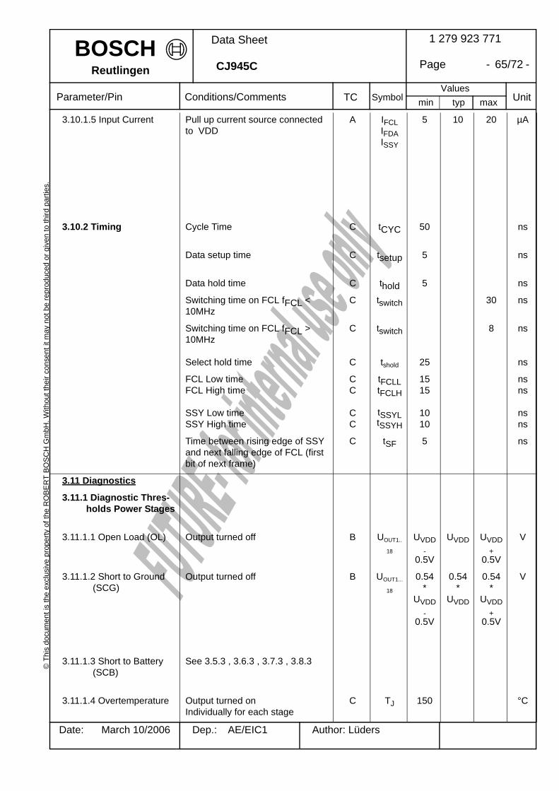
BOSCH©
Thi
s do
cum
ent i
s th
e ex
clus
ive
prop
erty
of t
he R
OB
ER
T BO
SC
H G
mbH
. With
out t
heir
cons
ent i
t may
not
be
repr
oduc
ed o
r giv
en to
third
par
ties.
typ maxminValues
Conditions/Comments
1 279 923 771
Page - 65/72 -
Date: March 10/2006 Dep.: AE/EIC1 Author: Lüders
Data Sheet
CJ945C
Parameter/Pin Symbol UnitTC
Reutlingen
3.10.1.5 Input Current Pull up current source connected to VDD
A IFCLIFDAISSY
5 10 20 µA
3.10.2 Timing Cycle Time C tCYC 50 ns
Data setup time C tsetup 5 ns
Data hold time C thold 5 ns
Switching time on FCL fFCL < 10MHz
C tswitch 30 ns
Switching time on FCL fFCL > 10MHz
Select hold time
C
C
tswitch
tshold 25
8 ns
ns
FCL Low timeFCL High time
SSY Low timeSSY High time
CC
CC
tFCLLtFCLH
tSSYLtSSYH
1515
1010
nsns
nsns
Time between rising edge of SSY and next falling edge of FCL (first bit of next frame)
C tSF 5 ns
3.11 Diagnostics
3.11.1 Diagnostic Thres-holds Power Stages
3.11.1.1 Open Load (OL) Output turned off B UOUT1..
18
UVDD-
0.5V
UVDD UVDD+
0.5V
V
3.11.1.2 Short to Ground (SCG)
Output turned off B UOUT1...
18
0.54 *
UVDD-
0.5V
0.54 *
UVDD
0.54 *
UVDD+
0.5V
V
3.11.1.3 Short to Battery (SCB)
See 3.5.3 , 3.6.3 , 3.7.3 , 3.8.3
3.11.1.4 Overtemperature Output turned onIndividually for each stage
C TJ 150 °C

BOSCH©
Thi
s do
cum
ent i
s th
e ex
clus
ive
prop
erty
of t
he R
OB
ER
T BO
SC
H G
mbH
. With
out t
heir
cons
ent i
t may
not
be
repr
oduc
ed o
r giv
en to
third
par
ties.
typ maxminValues
Conditions/Comments
1 279 923 771
Page - 66/72 -
Date: March 10/2006 Dep.: AE/EIC1 Author: Lüders
Data Sheet
CJ945C
Parameter/Pin Symbol UnitTC
Reutlingen
3.11.2 Bias Voltage Open Load Power Stages
Output turned off, IOUT1...18 = 0 A UOUT1...
18
0.6 *UVDD
0.7 *UVDD
0.76*UVDD
V
3.11.3 Diagnostic Cur-rents Power Stages
4.5V ≤ UVDD ≤ 5.5V, output turned off
UOUT1...18 = 14V (diagnostic cur-rent incl. leakage current)
UOUT1...18 = 0V
UOUT1...18 = OL-Threshold
UOUT1...18 = SCG-Threshold
A
A
C
C
IOUT
-IOUT
IOUT
-IOUT
270
50
220
40
580
130
980
250
980
250
µA
µA
µA
µA
3.11.4 Filtering Time Power Switches
Time from occurance of one of the errors ’short to ground’, ’open load’ or ’short to battery’ until the fault is entered into the corresponding diagnostic register.
Time from occurance of OT until the information is entered into the corresponding diagnostic register.
B
C
tDiag
tDiatOT
60
3
240
30
µs
µs
3.11.5 Diagnostic Thres-hold UBatt
Bit Ubatt in DIA_REG5 B Uth,UB 1 9 V
3.12 Reverse Currents
3.12.1 Reverse Current at OUT1...18 without Supply Voltage
UVDD ≤ 1V
Static
Dynamic (Test pulse 1 according to ISO: 100V, Ri = 10Ω, 2ms)
CCCC
CCCC
-IO1...6-IO9...16-IO7,8
-IO17,18
-IO1...6-IO9...16-IO7,8
-IO17,18
33
0.80.8
10101.51.5
AAAA
AAAA
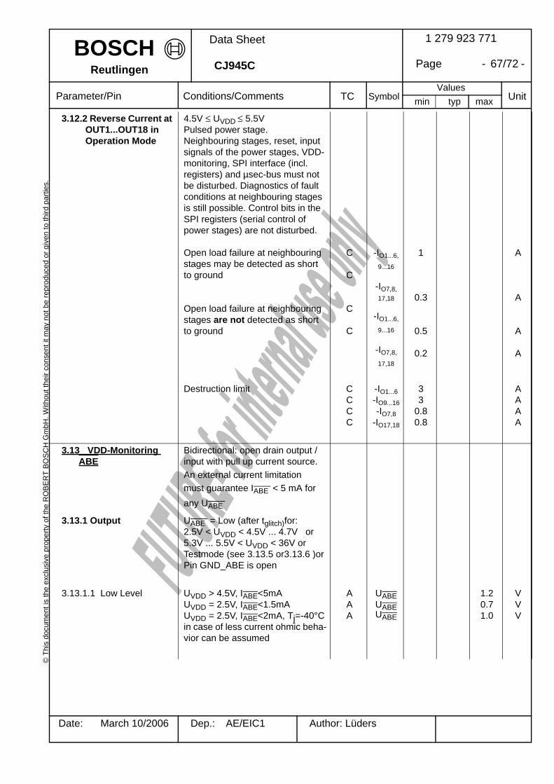
BOSCH©
Thi
s do
cum
ent i
s th
e ex
clus
ive
prop
erty
of t
he R
OB
ER
T BO
SC
H G
mbH
. With
out t
heir
cons
ent i
t may
not
be
repr
oduc
ed o
r giv
en to
third
par
ties.
typ maxminValues
Conditions/Comments
1 279 923 771
Page - 67/72 -
Date: March 10/2006 Dep.: AE/EIC1 Author: Lüders
Data Sheet
CJ945C
Parameter/Pin Symbol UnitTC
Reutlingen
3.12.2 Reverse Current at OUT1...OUT18 in Operation Mode
4.5V ≤ UVDD ≤ 5.5VPulsed power stage.Neighbouring stages, reset, input signals of the power stages, VDD-monitoring, SPI interface (incl. registers) and µsec-bus must not be disturbed. Diagnostics of fault conditions at neighbouring stages is still possible. Control bits in the SPI registers (serial control of power stages) are not disturbed.
Open load failure at neighbouring stages may be detected as short to ground
Open load failure at neighbouring stages are not detected as short to ground
C
C
C
C
-IO1...6,
9...16
-IO7,8,17,18
-IO1...6,
9...16
-IO7,8,
17,18
1
0.3
0.5
0.2
A
A
A
A
Destruction limit CCCC
-IO1...6-IO9...16-IO7,8
-IO17,18
33
0.80.8
AAAA
3.13 VDD-Monitoring ABE
Bidirectional: open drain output / input with pull up current source.An external current limitationmust guarantee IABE < 5 mA for any UABE
3.13.1 Output UABE = Low (after tglitch)for:2.5V < UVDD < 4.5V ... 4.7V or5.3V ... 5.5V < UVDD < 36V orTestmode (see 3.13.5 or3.13.6 )orPin GND_ABE is open
3.13.1.1 Low Level UVDD > 4.5V, IABE<5mAUVDD = 2.5V, IABE<1.5mAUVDD = 2.5V, IABE<2mA, Tj=-40°Cin case of less current ohmic beha-vior can be assumed
AAA
UABEUABEUABE
1.20.71.0
VVV

BOSCH©
Thi
s do
cum
ent i
s th
e ex
clus
ive
prop
erty
of t
he R
OB
ER
T BO
SC
H G
mbH
. With
out t
heir
cons
ent i
t may
not
be
repr
oduc
ed o
r giv
en to
third
par
ties.
typ maxminValues
Conditions/Comments
1 279 923 771
Page - 68/72 -
Date: March 10/2006 Dep.: AE/EIC1 Author: Lüders
Data Sheet
CJ945C
Parameter/Pin Symbol UnitTC
Reutlingen
3.13.1.2 Maximum Voltage No current recovery on VDD, UBatt and the logical pins (SS,SCK,SI,SO,INx,RST) in case of short to battery at ABE (up to 36V)
C UABE 36 V
3.13.2 Input
3.13.2.1 Low Level B UABEL 0.3 * UVDD
V
3.13.2.2 High Level B UABEH 0.7 * UVDD
V
3.13.2.3 Hysteresis C ∆UABE 0.2 1.0 V
3.13.2.4 Input Current Pull up current source connected to VDD
-0.3V ≤ UABE ≤ UVDD-1.5V A -IABE 20 40 100 µA
3.13.3 Overvoltage Thres-hold
Voltage referred to GND_ABE B VDDth_h 5.3 5.5 V
3.13.4 Undervoltage Threshold
Voltage referred to GND_ABE B VDDth_l 4.5 4.7 V
3.13.5 Test Mode:Reducing the Over-voltage Threshold
Voltage referred to GND_ABE B VDDth_h 4.5 4.7 V
3.13.6 Test Mode:Lifting the Under-voltage Threshold
Voltage referred to GND_ABE B VDDth_l 5.3 5.5 V
3.13.7 Suppression of Glitches
B tglitch 50 215 µs
3.13.8 GND_ABE
3.13.8.1 Permissible Offset between GND_ABE and GND
C ∆UGND 0.3 V
3.13.8.2 Bond Lift / Solder Crack on GND_ABE
Pin ABE goes LOW (see 3.13.1.1 ). The power stages are switched off.The over- and undervoltage thres-holds are increased by typically 700mV for TA = 25°C.
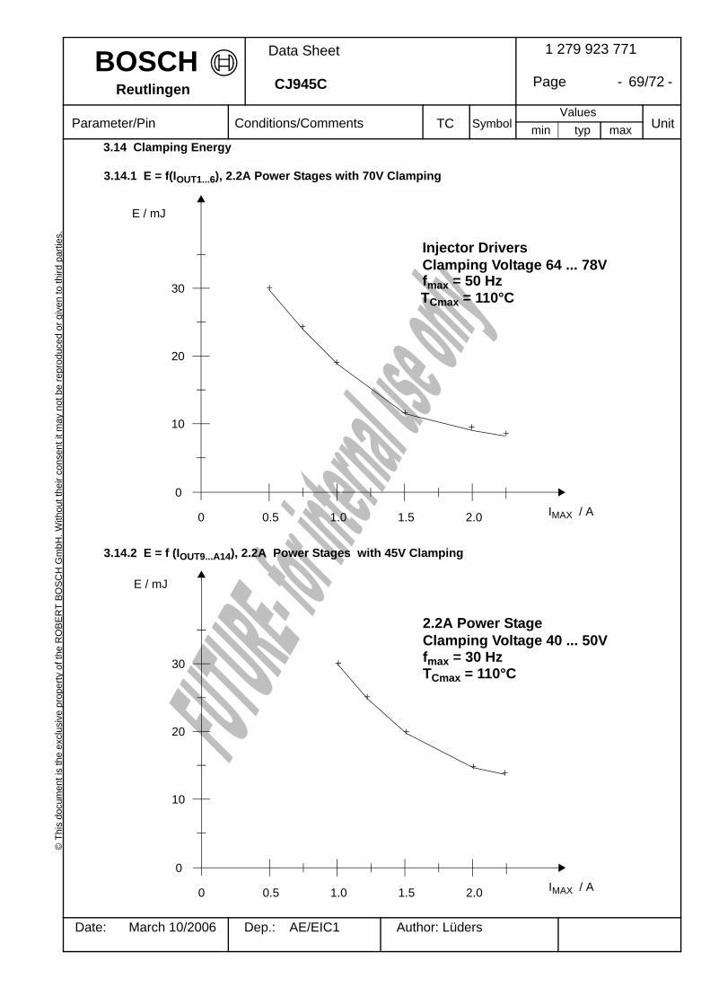
BOSCH©
Thi
s do
cum
ent i
s th
e ex
clus
ive
prop
erty
of t
he R
OB
ER
T BO
SC
H G
mbH
. With
out t
heir
cons
ent i
t may
not
be
repr
oduc
ed o
r giv
en to
third
par
ties.
typ maxminValues
Conditions/Comments
1 279 923 771
Page - 69/72 -
Date: March 10/2006 Dep.: AE/EIC1 Author: Lüders
Data Sheet
CJ945C
Parameter/Pin Symbol UnitTC
Reutlingen
3.14 Clamping Energy
3.14.1 E = f(IOUT1...6), 2.2A Power Stages with 70V Clamping
3.14.2 E = f (IOUT9...A14), 2.2A Power Stages with 45V Clamping
+
+
+
+
+
0 0.5 1.0 1.5 2.0
0
10
20
30
IMAX / A
Injector DriversClamping Voltage 64 ... 78V
+
TCmax = 110°Cfmax = 50 Hz
E / mJ
+
+
+
+ +
0 0.5 1.0 1.5 2.0
0
10
20
30
IMAX / A
2.2A Power StageClamping Voltage 40 ... 50V
E / mJ
fmax = 30 HzTCmax = 110°C

BOSCH©
Thi
s do
cum
ent i
s th
e ex
clus
ive
prop
erty
of t
he R
OB
ER
T BO
SC
H G
mbH
. With
out t
heir
cons
ent i
t may
not
be
repr
oduc
ed o
r giv
en to
third
par
ties.
typ maxminValues
Conditions/Comments
1 279 923 771
Page - 70/72 -
Date: March 10/2006 Dep.: AE/EIC1 Author: Lüders
Data Sheet
CJ945C
Parameter/Pin Symbol UnitTC
Reutlingen
3.14.3 E = f(IOUT7,8,17,18), 1100mA Power Stages with 45V Clamping
3.14.4 E = f(IOUT15, OUT16), 3.0A Power Stages with 45V Clamping
+
+
+
0 0.25 0.5 0.75 1.0
0
5
10
15
E / mJ
IMAX / A
1.1A Power StageClamping Voltage 40 ... 50V
fmax = 10 HzTCmax = 110°C
+
0 0.5 1.0 1.5 2.0
0
10
20
30
3.0A Power StageClamping Voltage 40 ... 50V
E / mJ
fmax = 30 HzTCmax = 110°C
2.5 IMAX / A
+
++
40
3.0

BOSCH©
Thi
s do
cum
ent i
s th
e ex
clus
ive
prop
erty
of t
he R
OB
ER
T BO
SC
H G
mbH
. With
out t
heir
cons
ent i
t may
not
be
repr
oduc
ed o
r giv
en to
third
par
ties.
typ maxminValues
Conditions/Comments
1 279 923 771
Page - 71/72 -
Date: March 10/2006 Dep.: AE/EIC1 Author: Lüders
Data Sheet
CJ945C
Parameter/Pin Symbol UnitTC
Reutlingen
4. EMI Requirements1)
see ‘Target Specification Power Stages CJ945’ (Y280 U61 868) from Dez/19/01.
5. ESD Capability
All pins of the IC are protected against electrostatic discharge (ESD) by appropriate protection components.
The integrated circuit meets the requirements of the „Human Body Model“ with UC = 2kV, C = 100pF and R2 = 1,5kΩ without any defect or destruction of the IC.
The ESD capability of the IC has been verified by the following test circuit.
UC = + 2kV
R1 = 100kΩ
R2 = 1,5kΩ
C = 100pF
Frequency: 1Hz
Arrangement and performance:The requirements of IEC 61340-3-1are fullfilled.The check of the ESD capability is performed with RB test specification 1 279 918 981 from 10/11/94.
DC-Volt-meter
R1 R2
C DUT
S2
S1
S3
US
(1) (2)
V UC
BOSCH©
Thi
s do
cum
ent i
s th
e ex
clus
ive
prop
erty
of t
he R
OB
ER
T BO
SC
H G
mbH
. With
out t
heir
cons
ent i
t may
not
be
repr
oduc
ed o
r giv
en to
third
par
ties.
typ maxminValues
Conditions/Comments
1 279 923 771
Page - 72/72 -
Date: March 10/2006 Dep.: AE/EIC1 Author: Lüders
Data Sheet
CJ945C
Parameter/Pin Symbol UnitTC
Reutlingen
6. ISO Pulses
For the definition of the ISO pulses the following standards have to be consulted:
ISO 7637-1 First Edition 1990-06-01
or
DIN 40 839 Part 1 Edition Oct. 1992
Signal shape and internal resistance for testing according to the standards above. For pulses 3a and3b, that have to be applied to CJ945, the following requirements upon the amplitudes have to be ob-served:
Pulse 3a: Us = -150VPulse 3b: Us = +100V
7. Quality Requirements
see ‘Target Specification Power Stages CJ945’ (Y280 U61 868) from Dez/19/01.