Embed Size (px)
Citation preview

BLOCK LEVEL V O L TA G E /FR EQ U E N C Y SCHEDULING FOR LOW PO W E R C O N SU M PTIO N
U N D E R TIM ING C O N STR A IN TS
A THESIS SUBMITTED IN PARTIAL FULFILLMENT OF THE REQUIREM ENTS FOR
THE DEGREE OF RESEARCH MASTER in the School
ofElectronic Engineering
byLi-Chuan Weng
B.Sc. ECE, National Chiao-Tung University, Taiwan September 2004
© Li-Chuan Weng 2004 DUBLIN CITY UNIVERSITY, IRELAND
All rights reserved.No p art of this work shall be reproduced,
in any form or by any means w ithout the permission from the author.

BLOCK LEVEL V O L TA G E /FR EQ U E N C Y SCHEDULING FOR LOW PO W ER C O N SU M PT IO N
U N D E R TIM ING C O N ST R A IN T S
Dissertation of Research M aster Degree School of Electronic Engineering
Dublin City University Ireland
byLi-Chuan W engSeptember 2004
Supervisor:Dr. XiaoJun Wang, Lecturer, Dublin City University
Interanl Examiner:Dr. Noel O ’Connor, Lecturer, Dublin City University
External Examiner:Dr. Steve Grainger, Professor, Staffordshire University

DeclarationI hereby certify that this material, which I now submit for assessment on the
program of study leading to the award of Research Master Degree of Electronic Engineering is entirely my own work and has not been taken from the work of others save and to the extent that such work has been cited and acknowledged within the text of my work.
Signed :
ID N o, M M *
Date : ^

To my parents

Acknowledgem ents
This thesis would not have been possible without my advisors, Dr. XiaoJun Wang and Dr. Alan P. Su. Many thanks to Dr. Wang for his inspiration and the time and patience spent in reading this thesis, thanks to Dr. Su for the discussions regarding to my research. Dr. Wang allowing me the freedom to work on topics th a t I enjoyed. I would like to acknowledge the help of Dr. Valentin Muresan with the contribution towards this thesis. Special thanks to my undergraduate mentors in ECE NCTU, Taiwan, including, but not limited to, Professor B.-F. Wu, D.-C. Liaw, K.-T. Song and to K.-Y. Yang. They are really kind teachers whom I am deeply indebted.
During these years of M aster research, I had the privilege of working in two environments, tha t both provided a pleasant and friendly place. The journey of this thesis began while I was in DCU, Ireland and continued after I started doing research in ITRI, Taiwan. Many thanks to all the technicians and faculties in EEng, DCU where I started my study and the colleagues at ITRI, where I finally completed this thesis.
This thesis could never be finished without the help and contributions of many friends and colleagues, therefore, I would like to especially thank my friends from everywhere in the world.
The friends I made while in Dublin were good companion and continue to bring joy into my life, these people include but not limited to Dr. J. K anatharana, E. Dautbegovic and E. Aviotte, who are like my sisters, the big Romanian community in EEng DCU, the basketball and volleyball sport group in DCU, friends from various corner around the world, and the overseas Taiwanese society in Ireland. I would never forget the encouragement friendship from them. They made my life full of

pleasure throughout the years spent in Dublin.There is a strong support from my friends back home during my abroad study.
The encouragement from them sustained me during the hard moments. Among them, I wish to express my appreciation to W.-P. Chen, C.-Y. Pan, C.-M. Wu. and Y.-H. Wu. They believed in me and provided support to me during the whole journey.
Last but not least, I want to express my gratitude to my family. I am deeply in debt to them. My deepest gratitude and love to my parents, without my m other’s encouragement I won’t be able to go through all the procedure. Thanks to my brothers Chia-Yang and Chia-Chun who support the family while I was abroad. At the end, I would like to dedicate this honor to my father, who was always nice to people but does not have chance to see this moment personally. His spirit always lives in my mind, now and forever.
It is impossible to list every single person who directly or indirectly company and help me to go through there years. I am very grateful to all the people who influenced my life during my past life and I do appreciate for your company in the rest journey. Thank you all.
• This work was supported in part by M inistry of Economic Affairs, Taiwan under project code A331XS1YR0, Power Aware SoC Using Dynamic Voltage/ Frequency Scheduling and Minimal Leakage Current input.
iv
Abstract
Over the past years, state-of-art power optimization methods move towards higher abstraction levels th a t result in more efficient power savings. Among existing power optimization approaches, dynamic power management (DPM) is considered to be one of the most effective strategies. Depending on abstraction levels, DPM can be implemented in different formats but here we focus on scheduling tha t is more suitable for real-time system design use. This differs from the concurrent scheduling approaches tha t s ta rt from either the HLS (High-Level Synthesis) or RTS (Real-Time System) point of view, we propose a synergy solution of both approaches, namely block-level voltage/frequency scheduling (BLVFS). The presented block-level voltage/frequency scheduling approach shows a generic solution for low power SoC (System on Chip) system design while the approaches which belong to the HLS and RTS categories have a strong dependency on the system functionalities. Consider a SoC as a combination of heterogeneous functional blocks, our approach provides efficient power savings by dynamically scheduling the scaling of voltage and frequency at the same time. Simulation results indicate tha t by using heuristic based strategies significant power savings can be achieved.K eyw ords: dynamic power management, scheduling, volt age/frequency scaling

Contents
Dedication iiAcknowledgements iiiAbstract vList o f Abbreviations xList of Symbols xi1 Introduction 1
1.1 M otivation ........................................................................................................... 11.2 Thesis S cope........................................................................................................ 1
1.2.1 High-level Synthesis for Low P o w e r ............................................... 21.2.2 Dynamic Power Management ......................................................... 21.2.3 Dynamic Voltage/Frequency Scheduling ..................................... 2
1.3 Thesis S tru c tu re .................................................................................................. 32 Theoretical Background 4
2.1 Preliminaries and In f ra s tru c tu re s ............................................................... 42.1.1 Sources of CMOS Power C o n su m p tio n ........................................ 42.1.2 Low Power Design T e rm in o lo g ies ................................................... 62.1.3 Power Optimization T e ch n iq u es ...................................................... 8
2.2 Low Power System Synthesis T e ch n iq u es .................................................. 102.3 DPM Methodology Based Approaches ..........................................................11
2.3.1 Power Down Related A p p ro a c h e s ................................................... 122.3.2 Scheduling Approach at System S y n th e s i s .................................. 142.3.3 Real-Time System Scheduling for Low P o w er.............................. 15
2.4 Voltage and Frequency Scaling M ech an ism ...................................................162.4.1 Voltage S c a l in g ..................................................................................... 162.4.2 Frequency S caling ................................................................................. 172.4.3 Dynamic Voltage and Frequency S c h e d u lin g .............................. 18
3 Problem Scope and Objective 203.1 Problem Scope ...................................................................................................... 213.2 Experimental M ethodology..................................................................................23
3.2.1 Design F ra m e w o rk ...................................................................................233.2.2 M athematical M o d e l ............................................................................... 25
3.3 Experimental S ch em e............................................................................................ 28
vi

3.3.1 N o ta tio n .......................................................................................................283.3.2 Quality M easurem ent............................................................................... 30
3.4 Objective and Expected A p p lica tio n s.............................................................314 Experim ental Scheduling 33
4.1 Scheduling S im u la to r ........................................................................................... 334.2 Block Level Dynamic Volt age/Frequency Scaling A lgorithm ....................354.3 Experimental R e s u lts ................. . ........................................................................374.4 Experimental Evaluation and C on clusion ...................................................... 43
5 Conclusion and Future Work 465.1 Summary and C onclusio ns................................................................................. 465.2 Future W o rk ............................................................................................................ 47
Bibliography 49Appendix A: Simulation Results of the First Testbench 55Appendix B: Power-related EDA Tools 57Appendix C: Publications 58Biographical Sketch 59
vii

List of Tables3.1 A table of delay and power ratios of the default setting modes ......................273.2 A table of parameters related to the ith operation period on the j th block . 294.1 Template of scheduling r e s u l t s ............................................................................ 354.2 List of supported voltage/frequency settings used in the experiment . . . . 374.3 Param eters of functional b l o c k s .........................................................................384.4 Voltage settings of the scheduling results for the first te s tb e n c h ...............394.5 Comparison of the four param eters before and after s c h e d u lin g ............... 414.6 Param eters of functional blocks in the second and th ird testb en ch ............42
viii

List of Figures2.1 Energy and power co m p a riso n ............................................................................... 72.2 Break-even time deduction ................................................................................. 132.3 Frequency scaling mechanism .......................................................................... 183.1 An internal view of a SoC architecture.................................................................213.2 Conceptual implementation of voltage/frequency scaling on c h i p ...................223.3 Comparison of energy consumption .................................................................... 243.4 Relationships between normalized power versus d e la y ....................................... 284.1 Process of the s im u la to r .........................................................................................344.2 Program pseudocode of the BLS algorithm .......................................................364.3 Comparison of power consumption before and after scheduling in the first
testbench .................................................................................................................... 414.4 Scheduling results of the second tes tbench .......................................................... 424.5 Scheduling results of the third testbench ..............................................................44

List of AbbreviationsACPI Advanced Configuration and Power InterfaceALAP As Late As PossibleASAP As Soon As PossibleBLS Block Level Dynamic Voltage/Frequency Scaling AlgorithmBLVFS Block Level Voltage/Frequency SchedulingCAD Com puter Aided DesignCFG Control Flow GraphCDFG C ontro l/D ata Flow GraphCMOS Complementary Metal-Oxide-SemiconductorCVS Clustered Voltage ScalingDFG D ata Flow GraphDFS Dynamic Frequency ScalingDP Dynamic ProgrammingDPM Dynamic Power ManagementDVFS Dynamic Voltage/Frequency SchedulingDVS Dynamic Voltage ScalingEDF Earliest Deadline FirstGALS Globally Asynchronous Locally SynchronousHDD Hard Drive DiskHLS High-Level SynthesisILP Integer Linear ProgrammingIP Intellectual PropertiesLEA Left-Edge AlgorithmNP Nondeterministic Polynomial-timeOS Operating SystemRM Rate MonotonicRMS Root Mean SquareRT Real-TimeRTL Register-Transfer-LevelRTOS Real-Time Operating SystemRTS Real Time SystemSoC System On ChipVLSI Very Large Scale Integration

List of Symbolsa : a process dependent param eter varies between 1 and 2, used for
circuit propagation delay 6 : propagation delayr : a set of operation periodTi : operation period ia : voltage factorb : frequency factorB : set of functional blocksB j : functional block jCj : average (effective) capacitor load of the j th functional blockCout : load capacitanceE : energyE ^ the energy consumption of block j during operation period iE\j : the energy consumption of block j during operation period i after
schedulingE sd : shutdown energy consumptionE totai : total energy consumption for the system during all operation peri
odsEwu : wake up energy consumption/ : working frequencyf : new working frequencyf ij : the working frequency of block j during operation period iF k : frequency setting at working mode kGj : transistor number of functional block j1leakage • leakage currentk : a process dependent constant, used for circuit propagation delayLi : usage list of operation period iMi : working mode kN : node transition activityNj : nod transition activity of functional block jP : power consumptionPavg : average power consumptionPdynamic : dynamic power consumptionPi : power consumption of operation period iPij : power consumption of block j during operation period iPieakage • due to the leakage current

p1 m ax the maximum power consumption over all system operationsPshort power consumption caused by short currentp1 static static power consumptionPswitching the switching component of powerPshort due to the direct-path short circuit currentPx rm s root mean square powerP s sleeping powerP w working powert timeU operation period it i j execution time of block j during operation period it total to tal execution time of a set of operation periodsTbe break-even timeTsd shutdown delayTto fixed timeoutTwu wake up delayVdd supply voltageVdd' new supply voltageV ij working voltage of block j during operation period iv k voltage at working mode kVt threshold voltage

Chapter 1
Introduction
1.1 M otivationNowadays, one of the most im portant considerations for VLSI/SoC designs is
low power. It is especially so for mobile platforms, not only for longer battery life but also for solving heat dissipation problems. Similar to other factors like area, performance, and reliability, the power issue should be taken into consideration at early design stages, i.e. at high levels, in order to achieve better efficiency. The work presented focuses on power minimization at system level by scheduling voltage and frequency scaling based on dynamic power management (DPM) policies.
1.2 Thesis ScopeLow power system design methods include power estim ation as well as power
minimization. Power minimization can be performed at various levels but is generally more effective at higher abstraction levels [CIB01]. Here we introduce some related survey methods of both power estim ation and power minimization. This investigation emphasizes the power minimization which is the wider scope of this thesis.
1

1.2.1 H igh-level Synthesis for Low Power
A high-level synthesis (HLS) system (also called, behavioral synthesis) takes a behavioral description of a design and produces a register-transfer-level (RTL) implementation of the design [BM99]. The synthesis process includes aspects such as scheduling, resource allocation, and binding. There are various approaches used in high-level synthesis for low power. Some people use integer linear programming (ILP) [JR97a] to schedule the voltage applied on a datapath in order to minimize power while others optimize transformation techniques like loop unrolling, pipelining, and retiming to achieve higher concurrency of a design in order to get a better architecture for lower power consumption [CB95].
1.2.2 Dynam ic Power M anagem ent
Dynamic Power Management (DPM) is considered to be the most powerful approach among the techniques for low-power design of integrated circuits and systems [BM98]. As a first glance, the fundamental idea of DPM is based on the fact tha t the workload of a system is not constant, and the DPM approach focuses on the u tilization of the slack tim e th a t is caused by the non-uniform workload [PR02, Wol02]. Unlike many existing approaches, DPM is actually an abstract concept tha t is independent of technology and can be applied at different abstraction levels. DPM research highlights the application of state transitions and tries to predict the system ’s working status in order to further reduce power dissipation [BBMOO].
1.2.3 Dynam ic V oltage/Frequency Scheduling
Status scheduling, i.e. to scale supply voltage and clock frequency according to available slack time, is an implementation of DPM. Putting a system into power down mode while idle is another way of implementing DPM. The characteristics of logic circuits are more suitable for dynamic voltage and frequency scheduling than power down and provides better results of power minimization [HPK99]. The

methodology uses the scheduling of voltage and frequency scaling to implement DPM. This thesis presents a heuristic based methodology th a t reduces power consumption in SoC through the control of voltage/frequency scaling.
1.3 Thesis StructureThis chapter has briefly introduced the thesis scope while the remainder of this
thesis is organized as follows. Chapter 2 describes the theoretical background, and covers the the sources of power consumption in Complementary Metal-Oxide- Semiconductor (CMOS) circuits. It is followed by descriptions of current power optimization methodologies, high-level synthesis for low power, with emphasis on contemporary dynamic power management methodologies. Chapter 3 describes the problem definition and the methodologies investigated here. This is followed by Chapter 4 where detailed algorithm and experimental results are presented. Finally, Chapter 5 concludes the thesis with a summary of the key contributions and the future research directions.
Chapter 2
Theoretical Background
Chapter 1 explained the motivations of power-aware design, and this chapter provides the related background. First, the related concepts and terminologies of low power CMOS VLSI circuits used throughout the thesis are introduced. Then, some of the relevant research fields including modern power optimization techniques, high-level synthesis for low power and dynamic power management are covered.
2.1 Preliminaries and InfrastructuresIn this section, we focus on power-related background th a t offers preliminaries for
the rest of this thesis. We first discuss the elements which cause power consumption in CMOS circuits, then we explain some terminologies used in the field of low power design tha t are often confusing. Finally, we briefly discuss some power optimization techniques.
2.1.1 Sources o f CMOS Power Consum ption
The starting point for low-power design is to understand where the power is consumed in a target system. Since CMOS devices are the most im portant cell elements in modern digital systems, we will examine the related contributing factors
4

of power consumption in CMOS systems. Generally speaking, the average power dissipation on CMOS devices can be decomposed into two parts as follows [CB95, Ped96, RP96, BM98, RPOO].
P iv g = P dynam ic P sta tic (2 -1)
From Equation 2.1, the two components of average power consumption are dynamic power (P dynam ic) and static power (P sta tic)• As implied by the name, static power is independent of the circuit activities but dependent on technology process. P sta tic is mainly caused by the leakage currents (I leakage) and occurs as long as power is supplied to the CMOS device. Since the factors tha t influence P sta tic are determined at manufacture, system designers have very little control of them, plus Pstatic is relatively small compared to Pdynamic> therefore, this thesis concentrates only on the minimization of P dyna m ic • It is worth noting tha t this assumption of P sta tic is much smaller than Pdynamic will change with the shrinking of feature size. It is predicated th a t P sta tic will be equal in proportion to Pdynam ic at about 45 nano — m eter scale technology.
The most significant source of CMOS power consumption is Pdynamic, it is dissipated as the circuit switches states. As shown in Equation 2.2, Pdynamic contains short-circuit power (Pshort) and switching power (P'switching) • Among the two elements, Pdynamic is subject to PSwitching resulting from charging and discharging the capacitive load (Cout) at the output of the gate.
Pdynam ic — P short Psw itching (2 -2 )
Here we emphasize on the minimization of P SWitching tha t dominates over 90% of the to ta l power dissipation and can be expressed by Equation 2.3:
P sw ithcing = N * Cout * V^d ' / (2-3)
There are four param eters in the equation above tha t can be considered to change [KL99], i.e. the node transition activity factor (N ), load capacitance (Cout), supplyvoltage (Vdd), and working frequency ( /) . Equation 2.3 dem onstrates tha t switchingpower consumption decreases quadratically with the decrease of Vdd and decreases linearly with the decrease of the other parameters. These param eters are targeted

for power optimization.From the above discussions, we can further approxim ate the power dissipated on
a CMOS circuit as Equation 2.4.
Pavg ~ Pdynam ic ~ Psvrithcing — N * ^out ' f (2-4)
Among the four param eters, N and Cout are mainly relevant at low levels of design, since Cout is highly dependent on the process technology and N is strongly dependent on the circuit activities. On the other hand, many approaches targeting Vdd and / focus on high level applications. The reason is tha t voltage and frequency can be controlled at higher levels although the implementation of the control mechanism also needs support from lower levels too. In order to exploit the fact th a t the voltage source has a quadratic influence on power consumption, the two most commonly used approaches are shutdown and scaling of supply voltage for power saving. A few frequency scaling approaches such as clock-gating or lowering frequency can also be found in the literature [RVB98, P C P +02]. The details regarding these approaches are explained in the following section. In this thesis, we intend to lower the power consumption by scaling down voltage and frequency at the same time.
2.1.2 Low Power D esign Terminologies
It is impossible to bring all aspects of power related design issues together in a single document. To avoid confusion, some concepts and terminologies tha t are usually used in the power-aware design field are listed here. Some of them are often used interchangeably but the minor differences between the definitions should be noticed.
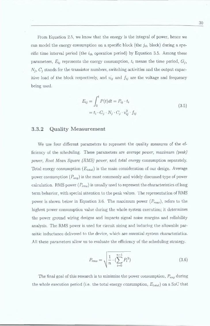
P ow er /E n e rg y . From Equation 2.5 and Figure 2.1 we can see tha t energy is the integral of power consumption over period of time, i.e. power is the curve and energy is the area underneath the curve. Compared to power, energy has a tem poral aspect tha t should be taken into consideration. In other words, even though power equals energy divided by time, the efficiency of power saving might sometimes be different from energy saving. Take battery-powered applications for

example, battery life is the main concern, therefore, energy is the focus rather than power in such systems. It might be possible to lower the average power consumption but extended execution time of a design, which could actually increase rather than decrease total energy consumption. The energy used purely to execute a task should be the same but extended execution tim e may mean more static power consumption and more leakage power.
E = [ P (t)d t (2.5)J o
Watts Pj: the height of the curve
E j: the area under the curve
► time
Figure 2.1: Energy and power comparison
A v erag e P o w er v .s . M a x im u m /P e a k P ow er. The average and maxim um /peak power are related but not the same. Maximum power deals with the worst case of a system while average power discusses the general situation. Based on the definition, it is trivial to see there is a difference between average power and m axim um /peak power consumption in a system [MK95]. In practice, there exists cases tha t lowering m axim um /peak power can cause the increasing of average power. The emphasis of this research is on the lowering of average power dissipation.
P o w er-aw are D esig n v .s . Low P o w er D esign . Low power design directly implies minimizing power/energy under certain constraints like performance. On the other hand, power aware design does not look for the lowest power but makes a tradeoff between the power and performance and may sometimes increase the power consumption instead of decreasing it [PR02, UK03]. In other words, power-aware

design may actually increase average power consumption in order to lower peak power consumption.
P o w er E s t im a tio n /S im u la t io n . Power related research can be classified as estim ation/evalutaion and optimization. Power estim ation and evaluation for systems is im portant during system design as it helps designers to meet the power requirements of the system specification. Further information can be found in the literature [MPS97, FGSS98, CIB01].
P ow er D is s ip a tio n /C o n s u m p tio n . Power dissipation is defined as the amount of energy dissipated, i.e. converted into another form of energy. On the other hand, power consumption implies the consumed energy from a power supply in unit time [PR02]. While power consumption relates to power delivery costs, performance and reliability, power dissipation affects more param eters including performance, packaging, reliability, environmental impacts and heat removal cost.
2.1.3 Power O ptim ization Techniques
A number of power optimization techniques have been proposed. Here we classify the research on power optimization along two axes, one is based on the target types and the other is according to the abstraction layers of logic circuit design.
M isce llan eo u s A p p ro a c h T y pes
The mainstream of power-related research is focused on CMOS circuits while there are miscellaneous ways to explore the system utilization. For instance, some research groups concentrate on battery models including battery capacity, discharge current etc. The domain of low power design is boundless, however, in this thesis we confine our core discussion to synchronous CMOS circuits. More specifically, we focus on a generic synchronous CMOS system, which is different from research that deals with specific circuits types, e.g. memory circuits, and asynchronous circuits. We concentrate on dynamic power only while some researchers concerned with other elements tha t cause power consumption like leakage current and glitches etc.
In widely used synchronous circuits, clock power can be a big portion of the over

all power dissipation. On the other hand, asynchronous logic or self-timed circuits use a handshaking scheme which does not need the clocks tha t usually consume significant power in the system. Therefore, some people work on asynchronous designs th a t operate w ithout an externally supplied clock as in [NCNvB94], the most dram atic self-timed example would be the research on AMULET processor cores [FEG+01]. Nevertheless, due to incompatibility with the current synchronous designs, this approach has not been widely discussed. There are approaches th a t mix synchronous with asynchronous design methodologies so as to take advantages of both sides, e.g. globally asynchronous locally synchronous (GALS). These mixed design methodologies supposedly have great potential [HMK+99]. Low power design covers a wide range of hardware and software design abstractions, discussions in the next paragraph focus on the techniques applied to the common synchronous circuits.
Low Power Synchronous Circuits
Optimization methods on CMOS circuits can be classified according to the design abstraction levels they are applied to, namely the layout level, device level, circuit level, logic level, architectural level, algorithmic level, and system level. Techniques applied at lower levels include dual supply voltage designs [UNI+97, CS99], multithreshold voltage, adiabatic circuits etc. The approaches at lower levels are more mature, but power optimizations should be addressed at both higher and lower levels in order to achieve better results. Comprehensive overviews on power optimization can be found in survey papers [RJD98, BdMOO, BBMOO, PedOl]. Detailed discussions about power dissipation at device level can be referred to [CPM+95, CB95]. Techniques applied at higher abstraction levels need to be addressed in order to efficiently manage power. Various approaches at system level have been used, including low-power module selection, power-conscious storage allocation and data mapping solutions, algebraic transform ations for low power, and operator shutdown etc. In addition, there are researches on power-efficient compilation approaches. System- level power optimization promises the most efficient approaches to low power design.

Approaches above System -level
The higher the abstraction level targeted the higher the efficiency. Currently, there are attem pts to manage the scheduling at operating system (OS) level or above, especially for real-time embedded systems. Some research is aimed at higher levels such as OS-level [LuOl, FM02], application level, and network layer, however, power optimization techniques at these levels are still at their infancy and more research is required. A complete classification of system level low power techniques for real-time systems can be found in [UK03]. Meanwhile, industrial standards like OnNow [Mic97] and Advanced Configuration and Power Interface (ACPI) [HPIM+] have been proposed to facilitate extreme high level power management. Combined with the current real-time system scheduling schemes, the full utilization of system level scheduling in low power applications can be expected soon.
2.2 Low Power System Synthesis TechniquesSystem synthesis (also known as behavioral synthesis) refers to the process of
mapping a high-level specification of a design into an RTL implementation [GVNG94]. Numerous researches on behavioral synthesis for low power have been conducted. In this section, we briefly review some of the most relevant contributions to the field of low power system synthesis with the main focus on scheduling methods.
The input of system-synthesis is some typical design representation in the form of data-flow graph (DFG), control-flow graph (CFG) or control/data flow graph (CDFG). DFG represents the essential ordering of operations in the program imposed by the data relations in the specification, CFG is derived directly from the explicit order given in the program and from the compiler’s choice of how to parse the arithmetic expressions, and CDFG is a heterogeneous model combined the CFG with DFG tha t can represent both the data dependence and the control sequence of a system in a single representation. The primary system synthesis steps are transformation , scheduling, allocation, and binding [Wol02]. Transformations for low power can be achieved by reducing the number of operators and thus the number of func-

tional units. Examples of applying transformations to the DFG of an algorithm that reduce the power consumption can be found in [CPM+95]. Allocation and binding carry out the selection and assignment processes of hardware resources for a given design. The aforementioned low power approaches like low power module selection and sharing belong to this category. We do not intend to describe the procedures in detail but more discussion can be found in the literature [Mic94].
2.3 DPM M ethodology Based ApproachesModelling and optimizing power at higher levels of abstraction are needed for
power-aware system designs. The reason tha t DPM can save power is based on the hypothesis th a t most systems are designed for peak use. The DPM strategy transits components into low-power states when they are idle in order to reduce energy. Basically, DPM is a powerful methodology th a t can be applied at several levels of abstraction. [BBMOO] is a survey of DPM related approaches. In other words, DPM strategies make a trade-off between power and performance. In this section, we focus on DPM methodology based scheduling approaches.
According to the policy characteristics, current DPM can be classified into heuristic and stochastic policies. Each category has its pros and cons yet there is no final conclusion regarding which is superior. In short, heuristic policies are easier to implement while stochastic policies guarantee optimized solution but are more complex to implement. The details of these strategies can be referred to in [QP99, CBM99, SBM01, SimOl] etc.
There are numerous ways to implement DPM methodology. To make use of the fact tha t energy consumption in CMOS circuits is quadratically proportional to its supply voltage, voltage shutdown and voltage scaling approaches are conceived. In short, voltage shutdown policies decide whether to switch on or switch off the supply voltage while voltage scaling strategies try to find a suitable voltage level for system /com ponent’s operation. The former ensures the power saving but has the drawback of losing performance due to the requirement of time to wake up. The latter is more suitable for real-time systems which have stringent execution-timing

requirements. It has been illustrated in [HPK99] th a t voltage scaling is superior to shutdown. The following investigation clarifies both power down and scaling approaches and indicates the significance of efficient DPM-centric scheduling approach.
2.3.1 Power Down R elated Approaches
To turn off power of an idle component is a radical way of thinking. Several mechanisms (e.g. supply voltage, Vdd and working frequency, f ) have been used for shutting down a device. Obviously, the most effective way to save power in idle modules is to shut down supply voltage, which reduces power dissipation to zero, hence shutdown has often been used in DPM methodology. It is worth emphasizing tha t power down does not imply only voltage shutdown th a t is the most commonly used approach but also includes other approaches such as clock gating, i.e. to gate the clock in order to freeze the clock of the idle device at RTL. The shutdown approach was firstly applied on mechanical devices like hard drive disks (HDD) [GBS+95] and was adopted in com puter systems and web servers. Since shutdown is the most common approach in power saving, systems or devices using the shutdown method are numerous.
According to the policies characteristics, shutdown methods can be categorized as static and dynamic ones. Static shutdown implies th a t the system does not change its prediction of tim eout period. A typical example of static shutdown is a fixed tim eout policy, in which components are transferred into power-saving mode after a certain threshold idle time. On the other hand, dynamic shutdown methods will try to predict the idle period, and there is no fixed waiting time before transferring idle components into power saving mode. A few shutdown approaches have been investigated and can be referred to [SCSOO].
The traditional shutdown approach turns off the power supply of the idle components and eliminates waste of power. Although shutdown does save power consumption during the shutdown period, it also incurs performance and power cost for state transitions. Some researches dynamically shutdown the idle components but such an approach is accompanied with penalties as well. This overhead occurred because of the need of power and tim e for state transitions, i.e. the transitions from working

state to shutdown state and vice versa. In order to explain whether shutdown is worthwhile, a concept called break-even time is used, i.e. the minimum length of idle time to achieve power saving [LM01], is defined as follows.
active
workingtime
Pw: working po;wer Twu: wake up delay : shutdown energy consumption Ps : sleeping power Tbe: break even time : wake up energy consumption TSd: shutdown delay
Figure 2.2: Break-even time deduction
Pw • t > E sd 4- E wu + Ps • (t — Tsd — Twu)4 ^ E sd + E w u — P s ‘ {T sd + T w u )
- P ^ P s (2-6)rp _ Esd + E wu — Ps • (TS(j + Twu)
be~ p - p1 w 1 s
If we do not consider the drawback of wake up delay but only consider fromthe energy point of view, the system should shutdown only when idle period t islonger than T&e. Figure 2.2 and Equation 2.6 explain the term 7&e. To sum up, the shutdown approaches should be applied only when the performance and power penalty is acceptable by using breakeven times as a metric to determine when to switch power states. A system should only be shutdown when its idle period t> T b e- For the same idle time, a longer break-even time means less power saving due to the overhead for recovering state [BBMOO]. Some approaches a ttem pt to predict the fluctuations in components’ workload in order to lower the waiting time caused by shutdown [HW97].

2.3.2 Scheduling Approach at System Synthesis
In this section we consider the application of system-level scheduling on low power designs. During the system synthesis process, scheduling determines the concurrency of the resulting implementation and affects system performance [Mic94]. Through scheduling, a sequencing graph developed from an algorithm ’s operand can determine the precise s ta rt time of each task while satisfying the original dependencies. The typical system-level scheduling problems can be modelled either unconstrained, such as the As Soon As Possible (ASAP) algorithm ; latency-constrained (the time available to execute the operations), such as the Late As Possible (ALAP) algorithm ; resource-constrained (the number of resources for each type of operation, e.g. adder, multiplier etc.) such as List Scheduling; or both resource and timing constrained scheduling, such as force-directed list scheduling. More detailed information on the conventional scheduling approaches may be found in reference [Mic94]. A number of researchers have developed systems or proposed methods tha t utilize high-level synthesis (HLS) for low power [JR97b, LHW97, HPK99, MC02, CIC+03] via scheduling, we survey some of them and explain the need for new strategies. Further review of existing approaches on HLS for low power can be referred to related literatures [JhaOl].
A number of algorithms using variable voltage settings with behavioral synthesis and datapath scheduling frequently appear in recent research [CP97, JR97a, SC98, HPK99, MC02, CIC+03]. These multiple voltage synthesis algorithms have some things in common. In short, they all attem pt to minimize energy consumption through the use of multiple voltages, many of them use DFG as algorithm input, and schedule different voltage levels on functional units such as adders, multipliers, registers etc. based on the infrastructural scheduling mechanisms including ASAP, ALAP and List Scheduling [RS95, LHW97, CP97, SC98, MC02]. Compared to the traditional HLS scheduling, there is an additional set of resource constraints in low power oriented HLS, th a t is, the corresponding operating voltages th a t can be used.
One of the first research tha t uses HLS scheduling for low power is [RS95], which schedules variable supply voltage on the datapath operators under timing constraints in order to minimize power. Both [JR97a] and [CP96] propose approaches to sched

ule working voltages of datapath operations from a specified list of candidate voltages to optimize power but use integer linear programming (ILP) and dynamic programming (DP) respectively. All the HLS approaches have the potential drawback tha t they have to rely on the system design, in other words, the mechanism they offer is limited by the example circuits or the benchmark suite they used ( e.g. EW Filter, AR Filter, DIFF EQ benchmarks are used by [CP97, SC98], [CIC+03] use ISCA89 benchmark suite). Another shortfall is that, these approaches are static and can not be applied dynamically hence they can not achieve the best optimization possible as it is difficult for the designer to foresee the variations of system operations. These approaches are therefore not generic as they can not be applied to complex hard real-time systems. Based on this thinking, a new strategy of operation period scheduling will be proposed in the next chapter.
2.3.3 Real-Tim e System Scheduling for Low Power
In real-time systems, the OS is in charge of scheduling programs according to their priorities. Scheduling algorithms guarantee timeliness of the task deadline. Typical real-time operating system (RTOS) scheduling approaches include Rate Monotonic (RM), Earliest Deadline First (EDF) techniques etc. The scheduling approaches can be classified as static scheduling and dynamic scheduling. The former one implies a fixed schedule which is determined at compile-time and hence it does not change at run time. The latter means the execution sequence is controlled or determined at run-time, or say, on-line.
As many embedded systems are real-time in nature, there has been some research working on different approaches using current real-time system scheduling techniques to further optimize power [HPS98, SC99, QWPOO, Gru02]. Such DPM approaches applied in RT scheduling for reducing energy consumption can be classified into CPU-centric and I/O centric classes. Most research [IY98, MC01, MC02, LXC03, YK03] belong to the first category and a few [SCI01, SC03] investigate the latter. The Dynamic Voltage Scaling (DVS) schemes tha t use existing RT scheduling to minimize the energy consumption while maintaining acceptable performance are processor-centric approaches. [YK03] has proved tha t optimal voltage scheduling

problem is NP-hard. Generally speaking, these approaches improve an existing task schedule with voltage and frequency scaling based on different modelling formulation and problem solving techniques (e.g. ILP).
2.4 Voltage and Frequency Scaling MechanismFor the sake of convenience, we repeat Equation 2.4 below, it is observed tha t
reduction of Vdd and/or / can save substantial power. In practical designs, voltage and frequency are closely related param eters and it should be possible to tackle both together for power saving purposes. The following discussions contain the current DVS and DFS (dynamic frequency scaling) mechanisms th a t are used as bases in this thesis.
Pavg ~ N ■ C m t 'V h ' f (2.7)
2.4.1 Voltage Scaling
As mentioned before, supply voltage Vdd is the most dominant factor tha t affects the power consumption of VLSI systems. An intuitive thinking is to lower the system supply voltage. However, aimlessly decreasing the supply voltage also increases the circuit delay, 8, given by Equation 2.8.
where k is a process dependent constant, Vt is the threshold voltage, and a is another process-dependent param eter which varies between 1 and 2. From Equation 2.8, the reason we can not simply lower supply voltage is, when the supply voltage is reduced to close to threshold voltage, the performance goals may not be met, even if we lower the threshold voltage at the meanwhile, it may make noise margin and leakage increase hence P sta tic increases. Also, the lowering of Vdd requires the decreasing of Vt which needs the support of the technology process and is beyond the control of system designers. In short, the smaller the Vdd, the higher the delay, so we have to
make a tradeoff between power saving and the increased circuit delay when voltage scaling is applied.
Based on the above discussion, we can further consider the relation of supply voltage and system performance. Most systems are over-designed in the way tha t system voltage is provided for maximum use. It is only natural to think of applying different voltage supply for different uses. High supply voltage implies high execution speed and is used for tasks with tight real-time constraints. On the other hand, lower supply voltage means lower execution speed and can be applied to tasks with loose time constraints.
DVS is a technique th a t promises substantial power reduction but we need to do smarter voltage management because simply lowering supply voltage also causes an increase of the delay. Most voltage scaling approaches require tha t the whole IC operates at the same supply voltage at the same tim e although the supply voltage could be different at different times, but DVS intends to scale the supply voltage according to the workload and get the benefit from it.
There is some research targeted at register-transfer-level (RTL) implementation with voltage scaling such as MOVER [JR97a], a tool which reduces the energy dissipation using datapath scheduling among multiple supply voltages. Some low level techniques like the Clustered Voltage Scaling (CVS) scheme uses two supply voltages VddH and VddL and the combination with Row by Row optimized Power supply scheme (RRPS) etc. [UH95, UNI+97, IUN+97]. In this thesis, we propose an original scheme tha t applies voltage scaling in the system, and an embedded selector in each functional block to achieve more efficient power savings.
2.4.2 Frequency Scaling
As the clock distribution network can consume dominant power in common synchronous circuits design, the clock is therefore another candidate for power minimization. Different from clock gating which stops the clock of idle components, Dynamic Frequency Scaling (DFS) reduces the power consumption by reducing the clock frequency of active components. However, lowering the frequency results in lowering the speed. In other words, it might lower the instant power but not the

total energy consumed. Here we do not want to ’’freeze” the clock but lower its performance. Compared to clock gating approaches, frequency scaling of synchronous circuits can be applied to more occasions according to system workload.
The literature on frequency scaling is relatively limited than the ones on clock gating. There are various works based on the frequency scaling idea but mainly for improving processor performance. The research on DFS for power minimization are relatively few apart from [RVB98, P C P +02]. We can use a clock divider to generate multiple clock frequencies based on a m aster clock as in [RVB96, RVB98]. To be more precise, we can use a control signal to select the appropriate output from the clock divider and use it as the clock input of a block. We can adopt this concept of frequency scaling and use the functional block as shown in Figure 2.3 to implement in circuit.
Figure 2.3: Frequency scaling mechanism
2.4.3 D ynam ic Voltage and Frequency Scheduling
Having established how DVS performs and disscussed how DFS works, it is now appropriate to introduce the Dynamic Voltage and Frequency Scheduling (DVFS) scheme which is proposed to tackle the power minimization problem in this thesis. The main idea of DVFS is to save energy by changing the working sta te of a system. The term, scheduling itself is actually ambiguous. As we discussed above, the current scheduling methodologies are based on either high level synthesis scheduling

or real-time scheduling. Our work does not fall into either of the two categories but incorporates features from both. We target the two factors th a t affect power dissipation mostly, i.e. voltage and frequency. The scheduling in our strategy is to deal with the scheduling of supply voltage and working frequency and adopt the concept of task deadlines in real-time scheduling. We are looking for effective scheduling techniques tha t treat voltage and frequency as variables to be determined, in addition to conventional task scheduling and allocation.

Chapter 3
Problem Scope and Objective
We intend to develop a DPM strategy which dynamically schedules the scaling of voltage and frequency, hence, our problem scope is to search for methods of DPM scheduling. So far, research into high-level DPM scheduling algorithms can be broadly divided into two categories: one th a t seeks power optimization at the synthesis stage, and the other starts from the real-time operating system scheduling. Here we first propose an approach tha t starts from the functional block level. This alternative strategy, which makes use of voltage and frequency scaling in HLS scheduling and task deadlines in RTS scheduling, can take advantages and avoid many drawbacks from both HLS scheduling and RTS scheduling. Before any further discussion on the methodologies and algorithm used in this dissertation, we explain the attem pted solving of the problem as well as the assumptions made in doing so. In this chapter, models and methods are presented by figures with explanations. The objective of our approach is to schedule voltage and frequency of functional blocks in a SoC system tha t is composed of heterogeneous components. Notice th a t here we do not distinguish between I/O devices and processors, instead treat all functional blocks the same. Based on DPM methodology, our final ta rget is to find a generic voltage/frequncy scheduling strategy to lower system power consumption.
20

3.1 Problem ScopeNowadays, tim e-to-m arket is an im portant issue in system design, many system
companies "reuse” and integrate pre-designed cores for new systems. Some vendors might adopt Intellectual Properties (IP) from different sources and use these IPs as functional units in their systems. W ithout loss of generality, in our experiments we consider a system as a combination of different functional blocks as shown in Figure 3.1, we do not consider the functionality of the blocks but trea t them as black boxes. This is because we care about the power consumption rather than the function of the blocks. Such abstraction and modularity provide a structural view of the overall system.
Figure 3.1: An internal view of a SoC architecture
Similar to many VLSI design autom ation problems, the volt age/frequency scheduling for power minimization is a nondeterministic polynomial-time decidable (N P- hard) problem. Looking for solutions to solve any NP-hard problem optimally is impractical. Hence we make certain assumptions to transform it into an NP-complete problem and look for efficient algorithms tha t provide near-optimum and acceptable solutions instead of finding exact optima since it is not polynomial time solvable. In this thesis, we use a heuristic algorithm to solve the voltage/frequency scheduling problem. For any NP-complete or NP-hard problems in CAD for VLSI, heuristics seems to be the only way to solve these problems.

22
As we do not distinguish functional blocks, this allows us to develop a higher abstract view of a system, and propose a power saving strategy based on a global view. Two alternative structures of the control mechanism are shown in Figure 3.2 (a) and (b). In either configuration, variable voltage/frequency can be set in individual functional blocks.
Vdd clock
i r n l t o n o / f r o n i m r t r t /
B lo ck i
voiiage/Trequencyrp m ila tn rre y u id iu r
1
voltage/frequencyregulator
B lo c k 2
voltage/frequency ■ . ■ ,
regulator
B lo ck3
B lo ck j
voltage/frequencyregulator
(a) external (b) internal
Figure 3.2: Conceptual implementation of voltage/frequency scaling on chip
Before we explain how we schedule the voltage/frequency settings, we first look at the question why do we use voltage and frequency as param eters to lower power. From Equation 2.3 we know th a t different param eters can be adjusted in order to lower the power. However, we concentrate only on the two param eters tha t can be controlled at system level, i.e. voltage and frequency. There have been research proposals using either voltage or frequency scaling to lower power consumption. However, considering the strong link between voltage and frequency, it is quite reasonable to design a mechanism tha t utilizes a combination of both to lower power consumption.
3.2 Experimental M ethodologyAs mentioned previously, a SoC is composed of a set of interacting components.
This functional block level view of a SoC makes it possible to select an appropriate voltage and frequency setting for each block according to its timing constraint. Our algorithm will generate a schedule, then select from a set of pre-defined supply voltage levels and frequency settings. Our approach combines voltage scaling with frequency scaling based on DPM principles. Some of the assumptions made throughout this thesis are summarized below.
1. The application programs are given in operation sequences tha t can be obtained in the specification, and we define th a t an operation period is generated whenever there are slack times.
2. The system provides a set of variable voltage/frequency settings for each individual component, i.e. the voltage/frequency on each functional block can be adjusted in different time intervals according to the calculated schedule. It is a trend to support multi-voltage and multi-frequency for SoC, and the implementation can be seen in the foreseeable future.
3. The power and time overhead caused by the sta te transition mechanism are relatively small and can be neglected.
4. The input switching activity N and the capacitive load C of each functional block remains the same before and after scheduling. Because at system level we can ignore minor fluctuations of N and C.
3.2.1 D esign Framework
The result of the scheduling is a schedule of the voltage/frequency settings for each functional block at different time intervals. For each operation, we first apply the maximum voltage/frequency on each functional block. For those blocks tha t are not on the critical path and with long slack time, we look for the lowest supply voltage and frequency setting tha t still gives non-negative slack time. Our approach

is then to search for the lowest volt age/frequency setting for each block tha t lowers the power consumption within the available slack time. Therefore, our approach attem pts to generate a schedule for the functional blocks along the time axis, and we scale the functional blocks’ voltage and frequency according to the schedule.
p
i
Eii
Eidle
t tU
t i : deadline of the i-th time interval t ij: time required to execute the task
in the i-th time interval on the j-th block Ey : energy consumed for the task
in the i-th time interval on the j-th block Eidie: energy wasted during the idle period P y : power consumption for i-th time interval on the j-th block Pidie: power consumption during idle period before scheduling
P
t i : deadline of the i-th time interval t 'ij: time required to execute the task
in the i-th time interval on the j-th block E’ij: energy consumed for the task
in thei-th time interval on the j-th block E'idie: energy wasted during the idle period after scheduling P 'ij: power consumption for i-th time interval on the j-th block P’idie: power consumption during idle period after scheduling
(a) Before scheduling (b) After scheduling
Figure 3.3: Comparison of energy consumption
Figure 3.3 graphically illustrates the mechanism we propose in this thesis. The main motivation for block-level scheduling comes from the fact tha t significant power can be saved by lowering supply voltage and working frequency. Consider the working status of a common functional block tha t works under maximum supply voltage/frequency. It happens very often tha t the operation has been completed well before the actual deadline (i.e. Uj is shorter than U) and this has the consequence of power wasted (E i(ne) as shown in the shadowed area in Figure 3.3 (a). After the completion of the operation, the component continues consuming power during Uj to ti. Although the power consumed during the slack time is slightly smaller than Pij, the energy wasted during this period is still dramatic. On the other hand, the approach proposed in this thesis is to adopt the concept of block-level scheduling th a t lowers voltage/frequency setting. By applying this scaling approach, the system can yield significant energy savings as presented in Figure 3.3 (b). From which, we see the execution time after scheduling • has been extended th a t accompanied

the lowering of the power P[-. By doing so, the values of and E[j in Figure 3.3 are actually the same, but the wasted energy in (b) E'idle during the slack time is much less than in (a) Eidie hence saves enormous energy. From the above discussions, we can understand why lowering voltage/frequency can provide significant energy savings. Under this scenario, the problem we attem pt to solve is to minimize the energy consumed by block-level voltage/frequency scheduling under given timing constraints. We then consider the hypothesis and assumptions more concretely in the next section.
3.2.2 M athem atical M odel
We use Equation 2.7 and Equation 2.8 to model the power and delay respectively. In order to compare the changes caused by scaling supply voltage and clock frequency, we use the following notations. First, the scaled voltage, Vdd, is denoted by the original supply voltage Vdd as well as a scaling factor a, i.e. Vdd = a • V^. As for the scaled clock frequency, it can be obtained by a similar relationship, / ' = 6 - / , where b is the frequency scaling factor. Consequently, we can use (V^, / ) and (aV^, b f ) to denote the voltage/frequency settings before and after scheduling respectively. The following are discussions of the power and timing models we used and the efficiency of our approach.Delay M odel
Equation 2.8 defines the strong dependency between propagation delay 6 and the supply voltage, Vdd, as well as the threshold voltage, Vt , i.e. 5 oc jy d̂ v t)a- On the other hand, clock frequency / is inversely proportional to circuit delay, i.e. <5 oc j , so we have the following relationship:
X Vdd 1 /q 1 \( 3 1 >
Let the working voltage and frequency be (V^, / ) before scheduling, and (aVdd, b f) after scheduling. In practical CMOS designs, the threshold voltage Vt ranges from 0 .2V to 0 .7V, and a is a constant varies between 1 and 2 depending on the technologies. According to the settings, the relationship between the propagation delay

before and after scheduling can then be represented by Equation 3.2.
<3-2>Power M odel
Equation 2.4 indicates the four factors th a t influence power consumption. As we want to emphasize the influences of voltage/frequency scaling on power consumption, we assume the first two param eters TV, and C remain the same before and after the scaling of frequency and voltage. Under such assumptions, the power equation can be conducted as P a • / . The relationship between new and original power can then be represented by Equation 3.3.
P(aVdd,b f) = a2b -P (V dd, f ) (3.3)System M odel
W ith the delay model and power model derived, we can now represent the delay time and power consumption as functions of the supply voltage and working frequency. The reason th a t we adopt both Vm and / in a fixed combination is due to the fact tha t the delay of combinational logic circuits increases with the decrease of supply voltage, therefore, it is necessary to lower the clock frequency according to the increased circuit delay, so th a t the state machine can work at the same cycle status. If we lower only the supply voltage, with the increased delay it can happen th a t the circuit does not work properly with the original clock frequency. On the other hand, simply scaling down the frequency itself does not save as much power as it would by scaling supply voltage at the time time as well. In other words, when scaling down the supply voltage, the clock frequency should also be appropriately scaled down. Consider a system tha t supports four different voltage/frequency settings, (5V, 80 MHz), (3.3V, 40 MHz), (2.4V, 20 MHz), (1.5V, 10 MHz), we can then represent the normalized relationships of delay and power of Equation 3.2 and Equation 3.3 in Table 3.1.
As the supported modes are given, we can easily get the voltage and frequency factors (a and b) by using (5V, 80 MHz) as the reference setting since it is the normal working mode. Based on a and 6, we then further calculate the delay ratio | • (aVdd-Vt)a an<̂ Power ra ti° a2k f°r each working mode. Take M2 for instance,

Table 3.1: A table of delay and power ratios of the default setting modes
setting (V, F) a b delay ratio1 power ratio2Mi (5V, 80 MHz) 1 1 1 1m 2 (3.3V, 40 MHz) 0.66 0.5 2.1213 0.2178m 3 (2.4V, 20 MHz) 0.48 0.25 3.7893 0.0576m 4 (1.5V, 10 MHz) 0.30 0.125 10.7991 0.0113
1,2 assume a = 1, Vt = 0.5 in Equation 3.2 and E quation 3.3 respectively.
the working voltage and clock frequency are 0.66 and 0.5 times the ones in mode M \. From the information in Table 3.1, we know the power consumption at mode M2 consumes only 21.78% of the power consumed at mode M \ as the power ratio explains, but this causes the delay which increases to 2.1213 times. By using these relationship and the available slack time, the working mode can then be transited to the lowest power cost mode while meets the timing constraint. Note tha t here we set a to 1 and Vt to 0.5 V for the sake of convenience, and we will use these settings for the example and experimental simulations in the next chapter.
W ith the param eters in Table 3.1, the execution time and power consumption as a function of mode transition is plotted in Figure 3.4. The horizontal axis is the power while the vertical axis represents the delay. The power and delay at mode Mi are used as a reference to quantize the variations of state transition in both axes, i.e. use the information provided in the two rightmost column in Table 3.1. It is importan t to say tha t m athem atically speaking the assumptions made overly simplify the modelling complexity, as we emphasize the scheduling strategy here so we assume some param eters like Nj and Cj remain the same before and after voltage/frequency scaling. On the other hand, it is im portant to mention tha t while our approach use the above settings to simulate the functions, the approach itself is universal and can be adopted to different system settings by using different scaling factors of a and b in Equation 3.2 and 3.3. In this thesis, we assume th a t all the functional blocks in the system support the same set of voltage/frequency combinations, but the algorithm proposed here does allow different voltage/frequency configuration for different functional blocks.

Figure 3.4: Relationships between normalized power versus delay
3.3 Experimental Scheme
3.3.1 N otation
The variables used in the notation are defined as follows. Three categories of variables are used. One set of variables with subscript i is used to indicate the attribute of the i th operation period. Another set of variables with subscript j is used to indicate the j th block characters. The last group of variables combines both i and j to indicate the param eter on the j th block during i th operation period. The inputs of our scheduling policy (the conditions of a given system) include the following items: a set T — { t i ,72, ...t*, ...rm} of m operation periods, a set B — {#!, jB2, ...B j , ...Bn} of n blocks and 5 settings of voltages and frequencies supported in the system, (V1, F 1), (V2, F 2), ...(K fc, V k} )...(V S, F s). Param eters associated with each operation period Tj £ T are listed below.
• the duration of each operation period: U

29
• a device usage list: L* consisting of the functional blocks needed in Tj
Each block Bj has the following parameters,
• transistor number: Gj
• average switching activity: Nj
• average (effective) capacitive load: Cj
Based on the above notations, we can further represent some individual param eters listed below.
• execution time of the i-th operation period on the j-th component: Uj
• voltage setting of the i-th operation period on the j-th component: the value of Vij equals to one of the voltage level settings supported in the system
• power consumption of the i-th operation period on the j-th component: P\j
• energy consumption of the i-th operation period on the j-th component: E{j
To avoid confusion, we summarize the param eters related to a block j and operation period i in Table 3.2.
Table 3.2: A table of parameters related to the ith operation period on the j th block
nBj (Vijifij')) ^ij5 P{j, Eij
The power consumed on a specific block for each individual operation period can then be represented by Equation 3.4 as follows.
P,j = Gj ■ N j ■ Cj ■ 4 • (3.4)
From Equation 2.5, we know th a t the energy is the integral of power, hence we can model the energy consumption on a specific block (the j th block) during a spe-
param eters, Eij represents the energy consumption, ti means the time period, G j, N j, Cj stands for the transistor numbers, switching activities and the output capacitive load of the block respectively, and v\j and f ij are the voltage and frequency being used.
3.3.2 Quality M easurem ent
We use four different param eters to represent the quality measures of the efficiency of the scheduling. These param eters are average power, maximum (peak) power, Root Mean Square (RM S) power, and total energy consumption separately. Total energy consumption (E totai) is the main consideration of our design. Average power consumption (Pavg) is the most commonly and widely discussed type of power calculation. RMS power (Prms) is usually used to represent the characteristics of long term behavior, with special attention to the peak values. The representation of RMS power is shown below in Equation 3.6. The maximum power (Pmax), refers to the highest power consumption value during the whole system execution; it determines the power ground wiring designs and impacts signal noise margins and reliability analysis. The RMS power is used for circuit sizing and inducing the allowable parasitic inductance delivered to the device, which are essential system characteristics. All these param eters allow us to evaluate the efficiency of the scheduling strategy.
cific time interval period (the i th operation period) by Equation 3.5. Among these
(3.5)= U ■ Gj ■ N j ■ Cj • v\j ■
n —1(3.6)
The final goal of this research is to minimize the power consumption, Pavg during the whole execution period (i.e. the total energy consumption, E totai) on a SoC tha t

is represented by Equation 3.7.m n
E to ta l = E E E ' i (3-7)»=1 j =1Although we focus mainly on the variations in total energy consumption, other param eters are used as an aid to understanding the characteristic changes before and after the scheduling.
3.4 Objective and Expected ApplicationsIn this dissertation we deal with the problem of minimizing the power consump
tion of a given SoC. The main idea of this approach is to reduce power by scaling the supply voltage and the clock frequency for components while meeting the timing constraint of the system. Based on DPM methodology, we can apply different voltages and clock frequencies to different components in a system within the available slack times, i.e. provide the same performance.
We constructed a model of a tem plate SoC system and developed a simulator. This computer-based simulator can carry out voltage/frequency scheduling and display the outcomes so tha t we can study the results and the behavior of the proposed algorithm. We model the system at a very-high abstraction level in which we view the system as a combination of functional blocks. The voltage and frequency of these functional blocks can be set to different states at different tim e intervals. Theoretically speaking, the more different settings supported in a system the more energy savings can be achieved. However, considering the current design, the voltage level settings for our simulator are adopted from literature [CP99] and listed as follows, {5V, 3.3V, 2.4V, 1.5V}. Corresponding to the provided voltages, the working frequencies are chosen as well. The key question is how to assign a proper speed to each operation period dynamically while guaranteeing all deadlines. We use a heuristic algorithm to find a good solution.
The problem we address is th a t of determining a schedule of voltage/frequency for the functional blocks such th a t the energy consumed by the system during the whole period E totai = N • ( S i l i ( S j = i Gj • Cj • V? • f ^ ) • ti) is minimized while ensur

ing tha t all operation periods meet their deadlines. The objective of our experiment is to find effective scheduling techniques th a t determine the voltage and frequency settings for each component in order to reach the goal of minimizing power. Our approach provides another alternative tha t can be considered a t the design stage.
The power increasing with growing density and complexity of digital systems can deteriorate the problem of power consumption very rapidly unless efficient approaches for managing system power are adopted. The disadvantage of a stochastic approach is the calculation complexity which can take much more time and circuit area than the heuristic ones. A simple heuristic is proposed here to find a voltage/frequency schedule which works sufficiently well.

Chapter 4
Experim ental Scheduling
Following the definition of the BLVFS problem in the last chapter, here we propose a Block Level Dynamic Voltage/Frequency Scaling (BLS) Algorithm to solve the BLVFS problem. After a detailed explanation of the algorithm, the simulation experiments of the algorithm are dem onstrated. The proposed algorithm has been implemented using Visual C + + . The experiments have been simulated under a Windows XP environment on a Pentium IV 2.8 GHz Personal Computer. Using the developed simulator, we simulate the scheduling using system settings th a t are given as inputs. All testbenches including environmental settings and system inputs were randomly generated. The param eters used in the random generation of each testbench like the settings of the work mode, information of operation periods and functional blocks etc. are set at the beginning of the simulation and used as inputs. After scheduling, the newly generated schedule is output in a text file.
4.1 Scheduling SimulatorFollowing the discussion of the proposed experiment scheme, we now introduce
the functions provided in the simulator. Figure 4.1 dem onstrates the process of the simulator graphically. The entire simulation environment includes the following elements:
33
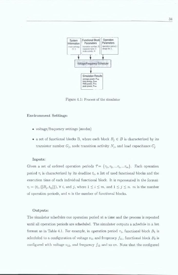
Figure 4.1: Process of the simulator
Environment Settings:
• voltage/frequency settings (modes)
• a set of functional blocks B, where each block Bj € B is characterized by its transistor number G j, node transition activity N j, and load capacitance Cj
Inputs:Given a set of ordered operation periods T = { t i ,72, ...7}, Each operationperiod 7* is characterized by its deadline a list of used functional blocks and the execution time of each individual functional block. It is represented in the format: Ti = {U, V 2, and j , where 1 < z < m, and 1 < j < n. m is the numberof operation periods, and n is the number of functional blocks.
Outputs:The simulator schedules one operation period a t a time and the process is repeated until all operation periods are scheduled. The simulator outputs a schedule in a list format as in Table 4.1. For example, in operation period t i , functional block B\ is scheduled to a configuration of voltage v n and frequency / n , functional block B^ is configured with voltage u12, and frequency /12 and so on. Note th a t the configured

settings of voltage and frequency {v ijjij) equals to one of the settings supported in the system.M easurement Expressions:
Table 4.1: Template of scheduling results
B i b 2nt2
fan , / n )(̂ 21 » / 2l)
{Vl2i / 12)(^22, f 22)
The final results include four measurement param eters th a t can be used to assess the quality of a schedule. They are total energy consumption E totah average power consumption Pavg, RMS power Prms and peak power Pmax. The evaluation param eters allow us to compare the alternative solutions to the problem. The proposed algorithm minimizes the average power consumption to achieve the target of lowering total energy consumption. The scheduling procedures of the heuristic algorithm are described in the following section along with its pseudocode.
4.2 Block Level Dynamic Voltage/Frequency Scaling Algorithm
In this section, we introduce the BLS algorithm. The operation of the BLS algorithm is based on a simple idea, i.e. for each functional block at each operation period, find out the lowest voltage/frequency settings th a t still meets the deadline of the operation period. The scheme of the BLS algorithm is simple, it consists of two iterations, i.e. operation periods and blocks. In the first step, all operation periods are scheduled with the normal voltage/frequency settings (i.e. 5V, 80 MHz) and the normal time needed for each functional block to complete its operation is known. The algorithm schedules one operation interval a t a time according to the order of the operation periods. For each operation period, a feasible schedule is found in the first step, in the second step the supply voltage and clock frequency are adjusted.

1 Given:2 - A list o f functional b locks that m ake up the system3 - A list o f supported w ork m odes, w here each m ode is co rresponding to its4 voltage/frequency setting5 - A sequence o f operation periods, w here each section is charac terized by its6 execution tim e tit the usage list L that contains the needed functional blocks7 - C alcu late the original Pjj, P ;, Ei, E,0tai, P»vg, Pm«> Pmax under the norm al8 voltage/frequency setting,9 - In itialize the total energy consum ption E,0tai10 F or (each operation period i, from i = / to m)11 {12 Initialize the pow er consum ption o f each operation period P ■, = 013 F or (each functional b lock j , from j= J to ti) //until all functional14 blocks are scheduled15 { /* m inim ize the pow er consum ed by each b lock fo r each16 operation period*/17 Try to find the low est voltage/frequency setting that still m eets18 the deadline19 R ecord the chosen m ode setting fo r the functional b lock20 C alcu late new Py21 U pdate Pi w ith the new Py com ponent22 } // end for23 C alcu late new E,=Pi * t„ update E lolai w ith new Ej com ponent24 }// end for25 C alcu late Pavg, P max, Prms
Figure 4.2: Program pseudocode of the BLS algorithm
Let us now look at the algorithm pseudocode in Figure 4.2. Assume tha t the system settings are initially given (line 2 to line 6). The measurement parameters at normal voltage/frequency setting are calculated. As can be figured out from the pseudocode itself, the algorithm is repeated until all the functional blocks are scaled in accordance with the operation sequence (line 10 to line 24). Before the scheduling starts, the param eters are initialized (line 9, line 12). The scaling process can be found in the inner fo r loop from line 13 to line 22. For each functional block, search for a lowest feasible voltage/frequency setting. Finally, we calculate E totai, Pavg, Prms, and Pmax- The algorithm generates a new optimized schedule from the input information. This BLS algorithm is an iterative heuristic th a t selects a feasible voltage/frequency setting for each functional block in a SoC at different time intervals.

4.3 Experimental ResultsExperimental results are reported in this section to dem onstrate the effective
ness of the proposed heuristic algorithms. We present the simulation results of some randomly generated testbenches for the algorithm. We use the total energy consumption Etotai before and after the voltage/frequency scaling to calculate the percentage of energy saved. In all three testbenches, we consider the systems support the voltage/frequency setting as in Table 4.2. The voltage settings are adopted from the literature [CP99], while the frequency settings are chosen according to the current system design.
Table 4.2: List of supported voltage/frequency settings used in the experiment
setting (v, F)Mi (5V, 80 MHz)m 2 (3.3V, 40 MHz)m 3 (2.4V, 20 MHz)m 4 (1.5V, 10 MHz)
The switching activity param eters N j of all functional blocks are set at 0.5 for the sake of convenience. The settings of each functional blocks like transistor number Gj and average capacitor load Cj are randomly generated at the beginning of simulation. These experiments test the impact of the scheduling algorithm. In each experiment, the results show the Pmax, Prms, Pavg, Etotai, and compare the efficiency of power savings.
The target of the experiment is to find a schedule of voltage/frequency settings th a t saves power while meeting the timing constraint. Prom Figure 3.4, we know tha t the delay of a functional block varies with the mode settings as shown in the delay ratio provided in Table 3.1. W ith the original execution time given as input, we can calculate the new execution time after voltage/frequency scaling, by multiplying the original execution time with the delay ratio and see whether the new execution time meets the tim ing constraints.

First TestbenchThe system here contains five functional blocks, and the related param eters are
given in Table 4.3 followed by the usage lists of the 10 execution periods. The total execution time of the set of the operation periods in the first experiment is 107 m s.
Table 4.3: Parameters of functional blocks
B ! b 2 B s B 4 B bG 41k 36k 40k 10k 31kN 0.5 0.5 0.5 0.5 0.5C 3pF IpF 5pF 4pF 5pF
n ( 6 , { [ # ! , 5 ] , [b 2 , 4 ] , [b 3 , 3 ] , [b 4 , i ]} )
r 2 ( 1 3 , { [ B i , 4 ] , [ B 2 , 1 ] , [ B 3> 2 ], [ B 4 , 1 2 ] , [ B 5 , 5 ]} )
r 3 ( 8 , { [ £ 3 , 3 ] , [ £ 4 , 4 ] , [ B 4 , 4 ]} )
t 4 ( 1 6 , { [ B i , 9 ] , [ B 2 , 2 ] , [ B 3> 1 0 ] , [ B 4 , 7 ] , [ B 5 , 5 ]} )
r 5 ( 8 , { [ B i , 4 ] , [ B 2) 6 ] , [ B 3 ) 6 ] , [ B 4 , 4 ] , [ B 5 , 2 ]} )
r 6 ( 1 4 , { [ B U 1 0 ] , [ B 2 , 1 3 ] , [ B 3 , 1 2 ] , [ B 4 , 7 ] , [ B 5 , 1 ]} )
7 7 ( 8 , { [ B i , 4 ] , [B 2 , 1 5 ] , [ B 3 , 3 ] , [ B 4 , 1 4 ] , [ B 5 , 1 5 ]} )
r 8 ( 2 , { [ B i , 1 ], [ B 2 , 1 ]} )
T9 ( 1 8 , { [ B 2 , 6 ] , [ B 3 , 1 ], [ B 4 , 1 2 ] , [ B 5 , 1 ]} )
r 10 ( 4 , { [ B i , 3 ] , [ B 2) 1 ], [ B 3 , 1], [ B 4 , 2 ] , [ B 5 , 2 ]} )
To interpret the input sequence, consider operation period T\ with ( 6 , {[#i, 5], [B2, 4], [J33, 3], [£?4, 1]}). In which, 6 represents the operation period in m s , and four functional blocks are used in this operation period, B\ to £?4. [Bi, 5] means the execution tim e of functional block B \ during the operation period T\ is 5 m s , in other words, there is 1 m s slack time. However, according to Table 3.1, the delay will be 2.1213 times longer after scaling down to the (3.3V, 40 MHz) setting which will result in deadline missing. This means we can not scale down the voltage/frequency

39
for functional block B Y a t the operation period T\ but should maintain B\ at the normal operation setting. During the same operation period, functional block B4 has a normal execution time of 1 m s. Scaling the operation setting down to (3.3V, 40 MHz) will still meet the deadline but not if scale down to (2.4V, 20 MHz), so we set ( v u j u ) = (3.3V, 40 MHz) for functional block J54 during the operation period r\. The scheduling results are shown in Table 4.4 with voltage settings only, as the voltage and frequency settings are in combined set so frequency settings are not listed here to avoid redundancy.
Table 4.4: Voltage settings of the scheduling results for the first testbench
Tl t 2 T3 t 4 t 5 t 7 t 8 T\ 0B i 5 3.3 0 5 5 5 3.3 5 0 5b 2 5 2.4 0 3.3 5 5 5 5 3.3 3.3B 3 5 3.3 3.3 5 5 5 3.3 0 2.4 3.3B 4 3.3 5 5 3.3 5 5 5 0 5 5b 5 0 3.3 5 3.3 3.3 2.4 5 0 2.4 5
Prom the information provided in Table 4.4, we then get the four measurement parameters (Etotah Pavg, Pmax, and Prms) by the following explanations. According to Equation 3 .4 , P^ = Gj • N j • Cj • vfj • fij. Consider the power consumption for the functional block B\ at operation period Tj, P n , th a t can be calculated by Equation
Pn = 41 k • 0.5 • 3 p • 52 • 80 M = 123 (unit power) (4.1)
For each specific (ith) operation period, we can calculate the power consumption Pi by Equation 4.2. The values of P* in each operation periods are used to represent the power transitions during whole period in Figure 4.3.
nPi = £ P* (4-2)
3 = 1

Based on the Pi, we can then get the other measurement param eters as follows.m
Etotai = ^ Pi • U = 29.61 (u n it energy) (4.3)i=l
Via total energy consumption, we can get the average power consumption by Equation 4.4 below, where t totai — 22=1 ti ~ 107 ms.
= — °-t-al- = 276.7 {unit power) (4.4)ttotaiand the maximum power,
Pmax ~ mCLX { P{ } (4-5)
In Equation 3.6, RMS power is defined as Prms = y j £ • (X ^ o ^»2)* Because each operation period has different execution time, we can not simply use Pi to calculate the Prms■ Equation 4.6 also takes into consideration of the execution time of each operation period as the weighting of each Pi in calculating Prms.
\.. m
— . ( £ P i 2 -U) (4.6)^total . «t=i
For the original energy consumption, we assume the system operates a t (5V, 80 MHz) setting for all functional blocks hence the the power consumption at each operation remains the same for whole system operation period 107 m s. Since there is no scaling of the voltage/frequency in the system, the average power equals both RMS power and maximum power (554 unitpower). The original energy consumption at settings without scheduling modification was 59.278 u n it energy while the one after the scheduling is 29.61 u n it energy which implies a saving of 50.05%. The RMS power is 304.4 u n it power, and the maximum power is 432.8 unit power. A comparison of the four param eters is listed in Table 4.5 below.
Figure 4.3 is used to represent the variation of Pi before scheduling (a) and after scheduling (b) along the time. In Figure 4.3 (b), the dark area implies the total energy consumption for the whole operation period and the white area in Figure 4.3 represents the energy saved. In the following testbenches, we use the same calculation process for the measurement param eters, but we do not give the detailed calculation again to avoid repetition. Detailed simulation results can be found in Appendix A.
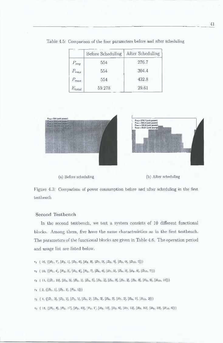
41
Table 4.5: Comparison of the four parameters before and after scheduling
Before Scheduling After Schedulingp1 avg 554 276.7P1 rms 554 304.4P1 max 554 432.8Etotai 59.278 29.61
(a) Before scheduling (b) After scheduling
Figure 4.3: Comparison of power consumption before and after scheduling in the first testbench
Second TestbenchIn the second testbench, we test a system consists of 10 different functional
blocks. Among them, five have the same characteristics as in the first testbench.The param eters of the functional blocks are given in Table 4.6. The operation periodand usage list are listed below.
n ( 16, {[Bi, 7], [B2, 1], [Bs, 6], [Be, 8], [B7, 9], [B8) 9], [Bfl, 9], [Bio, 2]})
r 2 ( 10, {[B u 4], [B2, 31, [B4, 61, [B5, 7j, [Be, 81, [B7, 5j, [B8, 3], [B», 8], [B10, 7]})
r3 ( 11, {[Bi, 10], [B2, 5], [B3, 1], [B4, 5], [B5, 2], [B6, 9], [B7, 2], [B8, 8], [B9, 9], [Bio, 10]})
t4 ( 2, {[Bi, 1], [BS, 1], [B9, 1]})
75 ( 4, {[Blt 3], [B2, 1], [B3) 1], [B4, 2], [B5, 2], [B6, 3], [£7, 2], [B8, 1], [B10, 2]})
r6 ( 18, {[Bi, 8], [B2, 17], [B3, 13], [B4) 1], [B5, 10], [B6, 6], [B7, 13], [B8, 10], [B9, 10], [Bio, 6]})
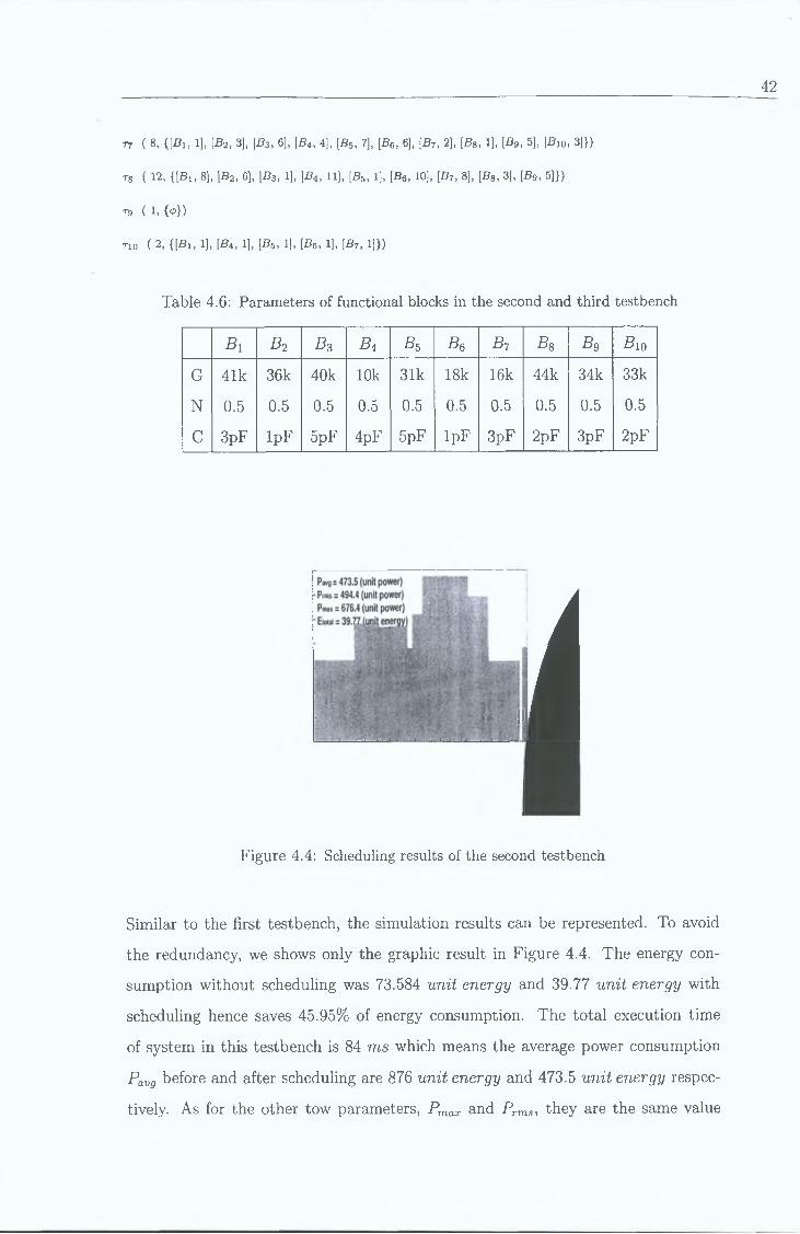
42
7Y ( 8, {[Bi, 1], [Ba, 3], [Bs, 6], [B4, 4], [B5) 7], [B6) 6], [B7, 2], [B8, 1], [B9, 5], [B10, 3]})
r 8 ( 12, {{Bi, 8], jB2, 6], IB3, 1], 1B4, 11], [B5, 1], [B6, 10], [B7, 8], [B8, 3], [B9, 5]})
tq ( 1 , {<£})
r 10 ( 2, {[Bi, 1], [B4, 1], [B5, 1], [B6, 1], [B7, 1]})
Table 4.6: Parameters of functional blocks in the second and third testbench
B 1 b 2 b 3 B 4 B b B q b 7 b 8 b 9 BioG 41k 36k 40k 10k 31k 18k 16k 44k 34k 33kN 0.5 0.5 0.5 0.5 0.5 0.5 0.5 0.5 0.5 0.5C 3pF IpF 5pF 4pF 5pF IpF 3pF 2pF 3pF 2pF
:: ■. . j; j
i
1Figure 4.4: Scheduling results of the second testbench
Similar to the first testbench, the simulation results can be represented. To avoid the redundancy, we shows only the graphic result in Figure 4.4. The energy consumption w ithout scheduling was 73.584 u nit energy and 39.77 u n it energy with scheduling hence saves 45.95% of energy consumption. The to ta l execution time of system in this testbench is 84 m s which means the average power consumption Pavg before and after scheduling are 876 unit energy and 473.5 un it energy respectively. As for the other tow parameters, Pmax and Prms, they are the same value

as the average power consumption before scheduling scheduling and the values after scheduling are shown in Figure 4.4.Third Testbench
Use the same components as in the second testbench to construct a system, but with 10 extra operation periods given below. The total execution time is 222 m s. The energy consumption after scheduling is 109.7 u n it energy, it represents a saving of 43.59 % compared to the 194.472 un it energy before the scheduling was applied. Similarly, the scheduling result is graphically shown in Figure 4.5. The original values of Pavg, PmaX) and Prms are all equal to 876 u n it energy and the values after scheduling are 494 unitpow er , 700 unitpow er , and 513.8 unitpow er respectively.
m ( 10, {[B2, 5], [#3, 6], [B4, 4], [£5, 1], [#6, 9], [B7, 9], [B8, 5], [£9, 3), [Bio, 4]})
r i 2 ( 14, {[Si, 11], IJB2, 4), (Bs, 6], [B4, 3], (B6, 13], [Be, 4], [B7, 10], [Bg, 7], [B9, 2], [Bio, 10]})
r 1 3 ( 14, { [B i, 5], [B2> 7], [B3 , 12], [B5 , 13], [B6 , 8 ], [B8 , 7], [B9> 2 ], [B io , H ]} )
r i 4 ( 18, { [B i, 11], [B a, 3], [B3 , 15], [B 4 , 2], [B 5 , 1], [B6 , 13], [B 7 , 5], [B x, 16], [B9 , 5], IB lf 6 ]})
T15 ( 18, {[B1( 13], [B2, 15], [B3, 12], [B4, 10], [B5, 13], [B6, 4], [B7, 2],[B9, 1], [Bio, 14]})
n« ( 9, {[Bx, 1], [B2, 1], [B3, 4], [B5, 1], [B6, 4], [B7, 6], [Bg, 6], [B», 4]})
t i t ( 4, {[Ba, 2], [B3, 1], [B4, 1], [B6, 2], [B7, 2], [B8, 2], [Bio, 2]})
n 8 ( 17, { [B i, 1 1 ], [Ba, 15], [B3 , 3], [B4 , 5], [B 5 , 3], [B q, 16], [B 7 , 7], [B s, 16], [B9 , 1 ], (B io , 10]})
n o ( 16, {[Bi, 7], [B2, 14], [B4, 14], [B5, 4], [B6, 3], [B7, 12], [B8, 6], [B9, 3], [Bio, 10]})
n o ( 18, { [B i, 8 ], [Ba, 8 ], [B3, 1 0 ], [B4 , 1 1 ], [B5 , 15], [B6 , 14], [B7, 11], [B8 , 12], [B9 , 10], [B io, 6 ]})
Based on the above simulations and the results in Figure 4.3, 4.4, and 4.5, we can see the dram atic energy savings by applying BLS algorithm in the system design.
4.4 Experimental Evaluation and ConclusionThe complexities of the original BLS algorithm is 0 (m n ), for m operation pe
riods and n functional blocks. Although the BLVFS problem itself is NP-complete

Figure 4.5: Scheduling results of the third testbench
in general, heuristic approaches can be used to solve the problem efficiently in polynomial time. This kind of sub-optimal solutions could be further improved by more sophisticated algorithms. The above simulations were done on system information generated randomly within the scope given beforehand. The experimental results prove tha t a BLVFS scheme can save significant energy. The main drawback with respect to simulative approaches is the lack of accurate power model. The scheduling algorithm can achieve better results (i.e. save more power) when the timing constraint is more loose as functional blocks can be set at modes with lower power consumption.
From the discussions of the innovative BLS algorithm, we see the most distinguishing point is its adaptivity in any system. For systems constructed by only a few types of functional blocks, there might be some chance to optimize the power usage by exploiting the common functional block characteristics in it. For this reason we also try to adapt the Left Edge Algorithm (LEA) to the BLVFS problem. The LEA is a track assignment algorithm and is famous for its application in channel-routing for minimizing the number of tracks used to connect nets on the channel boundary. LEA was then applied to register-allocation problem for minimizing the number of registers [KP87] and applied to block-level test scheduling problem for balancing
power dissipation during test [MurOl]. The basic idea of the LEA in BLVFS is to try to make full use of a functional block, and activate another functional block of the same type only if the current functional block can not perform all the required operations within available time. This means trying to schedule the same operations to a functional block while there is still slack time. For the simulations in this case, we consider systems th a t contain multi-functional blocks of the same type. Surprisingly, the simulation results are contrary to our expectation as we expected to further optimize the energy consumption by their similar characteristics. O ther than the problem th a t LEA does not perform better than BLS, there is another problem of using LEA since the design will require extra routing to transfer the workload between the functional blocks of the same type.
The work presented in this thesis is based mainly on voltage scaling coupled with frequency scaling. Note th a t our approach does not rely on any specific power model and is thus applicable to any power model. Even though it does not guarantee optimal voltage/frequency setting solutions, its final result can be used as a starting point by near-optimal block-level voltage/frequency scheduling approaches (e.g. simulated annealing, genetic algorithms, tabu search) to get improved solutions.

Chapter 5
Conclusion and Future Work
5.1 Summary and ConclusionsReducing power dissipation is a design goal for both portable and high end sys
tems. As most systems do not need peak performance at all time, it is possible to transit system components into low-power states by adjusting their frequency and voltage of operation while slack time exists. The whole thesis surrounds a DPM methodology tha t can gain significant power savings. The aim of this thesis is to propose a novel voltage and frequency scaling scheme at functional block level tha t can be applied at run-time. We discussed power optimization in Chapter 2. Both heuristic and stochastic DPM methodologies can be applied in power down and voltage/frequency scaling approaches. In this thesis, our target is to lower Pdynamic of a SoC at system level, so we focus on voltage and frequency which can be managed by system designers.
BLVFS takes the advantage of the fact th a t typical modern systems are over- designed and IPs have become widely used in the industry. The algorithm aims at stretching the execution time of the functional blocks in each operation period through voltage/frequency scaling. For real-time SoCs, the proposed BLVFS scheme focuses on minimizing energy consumption, while still meeting the performance requirements. In order to simplify the analysis and to allow for the derivation of analytical formulas, we assume N and C are not affected by voltage and frequency
46

scaling during simulation. The primary advantage of BLVFS is its conceptual simplicity and adaptivity. The proposed heuristic for block level voltage and frequency scaling is of low complexity, yet it can generate close to optimal solutions.
This thesis presents a study of BLVFS in order to derive a new approach th a t can minimize power consumption. Designers focus on worst-case circumstances, therefore, power management exploits idleness resulting from system under-utilization. We proposed a tentative algorithm for possible implementation of voltage and frequency scaling. Heuristic algorithms generally need shorter run-time than stochastic algorithms hence they are more suitable for real-time use. The difference from the conventional techniques is th a t the proposed methodology is very flexible and can be extended to various other applications. The main contributions of this thesis is to provide an innovative BLVFS idea and to prove the efficiency of the proposed heuristics for dram atic power savings. Besides, since the short-circuit power Pshort is approximately proportional to (Vdd — 2 • Vth)3 so the short-circuit power is also consequently reduced with the lowering of the supply voltage.
5.2 Future WorkFuture work includes three main directions. One is to further research the algo
rithm s tha t can be applied to the BLVFS problem in order to further optimize the scheduling results. The second research direction is to investigate the applicability of the BLVFS in practical circuit designs, i.e. hardware implementation issues. The third direction is to combine the BLVFS method with other power-aware design considerations like power estimation and static power minimization, etc.
The previous chapters have provided a first look a t the issues involved in BLVFS problems and proposed greedy heuristics. We expect to see the use of optimization heuristics like tabu search, simulated annealing, and generic algorithm etc. to solve the BLVFS problem in the near future. Many real-time SoC systems can be modelled using our approach, we can generalize our approach to handle more general models like dependent operation interactions, and preemptive scheduling cases.
To implement the BLVFS in a system tha t scales the working voltage and fre
quency will mean some extra control unit, i.e. the implementation of high-efficiency DC-DC converters and frequency dividers in hardware. The power management schemes make a complex tradeoff between power, speed, and area whereas we emphasize only the first two in the algorithm, there is also power and time cost of the extra control unit need to be considered. Future work should look at the practical implementation aspects involved, to combine resource allocation and other lower level design approaches along with the scaling algorithm so th a t the whole system design is optimized, for instance, the consideration of the consequential implementation issues during binding and layout stage should be further discussed as well [Wol02].
The discussions in this thesis focus on the dominant component of power consumption, Pdynamic, however, with the shrinking of feature size, static power dissipation, Pstatic will increase to the same level as Pdynamic• Further investigation of leakage power and glitch should be taken into account for future research directions.
The proposed algorithm in this thesis can be viewed as the beginning of a mechanism to support low power design. In the course of time, the BLVFS scheme may provide a distinctively different dimension for low power designs as compared to classical techniques tha t are problem-specific. To improve the design accuracy, there is the need for cycle-accurate power estimation of functional modules. System designers lack high-level CAD tools to support power-related design issues so far (see Appendix B). In the commercial arena, we have not seen an efficient solution so we would stress again the need of Electronic Design Autom ation (EDA) tools to encapsulate the current approaches th a t provides power managing scheme at early stage. So far, the system and high level power-aware design is still in its infancy and needs more efforts.

Bibliography[BBMOO]
[BdMOO]
[BM98]
[BM99]
[CB95]
[CBM99]
[CIB01]
[CIC+03]
[CP96]
Luca Benini, Alessandro Bogliolo, and Giovanni De Micheli. A survey of design techniques for system-level dynamic power management. IEEE Transactions on Very Large Scale Integration Systems, 8(3):299—316, June 2000.Luca Benini and Giovanni de Micheli. System-level power optimization: techniques and tools. AC M Transactions on Design Automation of Electronic Systems, 5(2) :115—192, 2000.Luca Benini and Giovanni De Micheli. Dynamic power management - design techniques and CAD tools. Kluwer Academic Publishers, 1998.Luca Benini and Giovanni De Micheli. System-level power optimization: techniques and tools. In Proceedings 1999 international symposium on Low power electronics and design, pages 288-293. ACM Press, 1999.A nantha P. Chandrakasan and Robert W. Brodersen. Low power digital CMOS design. Kluwer Academic Publishers, 1995.Eui-Young Chung, Luca Benini, and Giovanni De Micheli. Dynamic power management using adaptive learning tree. In Proceeding of the 1999 international conference on Computer-aided design, pages 274- 279. IEEE, 1999.R ita Yu Chen, Mary Jane Irwin, and Raminder S. Bajwa. Architecture- level power estimation and design experiments. ACM Transactions on Design Automation of Electronic Systems, 6(l):50-66, 2001.Noureddine Chabini, Ismail, Chabini, El M ostapha Aboulhamid, and Yvon Savaria. Methods for minimizing dynamic power consumption in synchronous designs with multiple supply voltages. IEEE Transactions on Computer-Aided Design of Integrated Circuits and Systems, 22(3):346-351, 3 2003.Jue-Ming Chang and Massoud Pedram. Energy minimization using multiple supply voltages. In Proceedings of the 1996 international symposium on Low power electronics and design, pages 157-162. IEEE, 1996.
49
[CP97]
[CP99]
[CPM+95]
[CS99]
[FEG+01]
[FGSS98]
[FM02]
[GBS+95]
[Gru02]
[GVNG94]
[HMK+99]
[HPIM+]
[HPK99]
Jue-Ming Chang and Massoud Pedram. Energy minimization using multiple supply voltages. IEEE Transactions on Very Large Scale Integration Systems, 5(4):436-443, 12 1997.Jue-Ming Chang and Massoud Pedram. Power Optimization and Synthesis at Behavioral and System Levels Using Formal Methods. Kluwer Academic Publishers, 1999.A nantha P. Chandrakasan, Miodrag Potkonjak, Renu Mehra, Jan Rabaey, and Robert W. Brodersen. Optimizing power using transformations. IEEE Transactions on Computer-Aided Design of Integrated Circuits and System s, 14(1): 12-31, 1 1995.Chunhong Chen and Majid Sarrafzadeh. Provably good algorithm for low power consumption with dual supply voltages. In Proceeding of the 1999 international conference on Computer-aided design, pages 76-79. IEEE, 1999.S.B. Furber, A. Efthymiou, J.D. Garside, D.W. Lloyd, M.J.G. Lewis, and S. Temple. Power management in the amulet microprocessors. IEEE Design and Test of Computers, 18(2):42-52, March-April 2001.William Fornaciari, Paolo Gubian, Donatella Sciuto, and Christina Sil- vano. Power estim ation of embedded systems: a hardware/software codesign approach. IEEE Transactions on Very Large Scale Integration Systems, 6(2):266-275, 6 1998.Krisztian F lautner and Trevor Mudge. Vertigo: Automaticperformance-setting for linux. In OSDI, 2002.Richard Golding, Peter Bosch, Carl Staelin, Tim Sullivan, and John Wilkes. Idleness is not sloth. In Proceedings of the W inter Usenix Conference, pages 201-212, 1995.Flavius Gruian. Energy-centric scheduling for real-time systems. PhD thesis, Lund University, 11 2002.Daniel D. Gajski, Frank Vahid, Sanjiv Narayan, and Jie Gong. Specification and design of embedded systems. Prentice Hall, 1994.A. Hemani, T. Meincke, S. Kumar, A. Postula, T. Olsson, P. Nilsson, J. Oberg, P. Ellervee, and D. Lundqvist. Lowering power consumption in clock by using globally asynchronous locally synchronous design style. In Proceedings of the 36th A C M /IE E E conference on Design automation conference, pages 873-878. ACM Press, 1999.Hewlett-Packard, Intel, Microsoft, Phoenix, and Toshiba. Advanced configuration and power interface. [Online] http://w w w .acpi.info.Inki Hong, Miodrag Potkonjak, and Ramesh Karri. Power optimization using divide-and-conquer techniques for minimization of the number of operations. AC M Transactions on Design Automation of Electronic Systems, 4(4):405-429, 1999.

[HPS98]
[HW97]
[IUN+97]
[IY98]
[JhaOl]
[JR97a]
[JR97b]
[KL99]
[KP87]
[LHW97]
[LMOl]
[LuOl]
Inki Hong, Miodrag Potkonjak, and Mani B. Srivastava. On-line scheduling of hard real-time tasks on variable voltage processor. In Proceedings o f the 1998 IE E E /A C M international conference on Computer- aided design, pages 653-656. ACM, 1998.Chi-Hong Hwang and Allen C.-H. Wu. A predictive system shutdown m ethod for energy saving of event-driven computation. In Proceedings of the 1997 IE E E /A C M international conference on Computer-aided design, pages 28-32. IEEE, 1997.M utsunori Igarashi, Kimiyoshi Usami, Kazutaka Nogami, Fumihiro Minami, Yukio Kawasaki, Takahiro Aoki, Midori Takano, Chiharo Mizuno, Takashi Ishikawa, Masahiro Kanazawa, Shinji Sonoda, Makoto Ichida, and Naoyuki Hatanaka. A low-power design method using multiple supply voltages. In Proceedings o f the 1997 international symposium on Low power electronics and design, pages 36-41. ACM, 1997.Tohru Ishihara and Hiroto Yasuura. Voltage scheduling problem for dynamically variable voltage processors. In Proceedings 1998 international symposium on Low power electronics and design, pages 197-202. ACM, 1998.Niraj K. Jha. Low power system scheduling and synthesis. In Proceedings of the 2001 IE E E /A C M international conference on Computer- aided design, pages 259-263, 2001.Mark C. Johnson and Kaushik Roy. D atapath scheduling with multiple supply voltages and level converters. AC M Transactions on Design Automation o f Electronic System s, 2(3):227-248, 1997.Mark C. Johnson and Kaushik Roy. Scheduling and optimal voltage selection for low power multi-voltage dsp datapaths. In Proceedings of the 1997 IEEE International Symposium on Circuits and Systems, pages 2152-2155. IEEE, 1997.James B. Kuo and Jea-Hong Lou. Low-voltage CMOS VLSI circuits. Wiley-Interscience, 1999.Fadi J. Kurdahi and Alice C. Parker. Real: A program for register allocation. In 24th A C M /IE E E Design Automation Conference, pages 210-215, 1987.Yann-Rue Lin, Cheng-Tsung Hwang, and Allen C.-H. Wu. Scheduling techniques for variable voltage low power designs. ACM Transactions on Design Automation of Electronic Systems, 2(2):81-97, April 1997.Yung-Hsiang Lu and Giovanni De Micheli. Comparing system-level power management. IEEE Design and Test o f Computers, 18(2): 10-19, March-April 2001.Yung-Hsiang Lu. Power-aware operating systems for interactive systems. PhD thesis, Stanford University, December 2001.
[LXC03]
[MC01]
[MC02]
[Mic94]
[Mic97][MK95]
[MPS97]
[MurOl]
[NCNvB94]
[PCP+02]
[Ped96]
[PedOl]
Dexin Li, Qiang Xie, and Pai H. Chou. Scalable modeling and optimization of mode transitions based on decoupled power management architecture. In Proceedings of the 2003 Design Automation Conference. ACM, 2003.Ali Manzak and Chaitali Chakrabarti. Variable voltage task scheduling algorithms for minimizing energy. In Proceedings o f the 2001 international symposium on Low power electronics and design, pages 279-282. ACM, 2001.Ali Manzak and Chaitali Chakrabarti. A low power scheduling scheme with resources operating at multiple voltages. IEEE Transactions on Very Large Scale Integration Systems,, 10(1):6—14, February 2002.Giovanni De Micheli. Synthesis and optimization of digital circuits. McGraw-Hill, 1994.Microsoft. Onnow: the evolution of the pc platform, 1997.Raul San M artin and John P. Knight. Power-profiler: optimizing asics power consumption at the behavioral level. In Proceedings of the 32nd A C M /IE E E conference on Design automation conference, pages 42-47. ACM, 1995.Enrico Macii, Massoud Pedram, and Fabio Somenzi. High-level power modeling, estimation, and optimization. In Proceedings o f the 34th annual conference on Design automation conference, pages 504-511. ACM, 1997.Valentin Muresan. Block-level Test Scheduling under Power Dissipation Constraints. Ph. d thesis, Dublin City University, December 2001.Lars S. Nielsen, Jens Sparso Cees Niessen, and Kees van Berkel. Low- power operation using self-timed circuits and adaptive scaling of the supply voltage. Very Large Scale Integration (VLSI) Systems, IEEE Transactions on, 2(4):391-397, December 1994.Kiran Puttaswamy, Kyu-Won Choi, Jun Cheol Park, III Vincent J. Mooney, Abhijit Chatterjee, and Peeter Ellervee. System level power- performance trade-offs in embedded systems using voltage and frequency scaling of off-chip buses and memory. In Proceedings of the 15th international symposium on System Synthesis, pages 225-230. ACM, 2002 .
Massoud Pedram. Power minimization in ic design: principles and applications. AC M Transactions on Design Automation of Electronic Systems (TODAES), 1(1):3—56, January 1996.Massoud Pedram. Power optimization and management in embedded systems. In Proceedings of the conference on Asia South Pacific Design Automation Conference, pages 239-244. ACM, 2001.
[PR02]
[QP99]
[QWPOO]
[RJD98]
[RP96]
[RPOO]
[RS95]
[RVB96]
[RVB98]
[SBMOl]
[SC98]
[SC99]
Massoud Pedram and Jan Rabaey. Power aware design methodologies. Kluwer Academic Publishers, 2002.Qinru Qiu and Massoud Pedram. Dynamic power management based on continuous-time markov decision processes. In Proceedings of the 36th A C M /IE E E conference on Design automation conference, pages 555-561. ACM, 1999.Qinru Qiu, Qing Wu, and Massoud Pedram. Dynamic power management of complex systems using generalized stochastic petri nets. In Proceedings of the 37th conference on Design automation, pages 352- 356. ACM, 2000.Anand Raghunathan, Niraj K. Jha, and Sujit Dey. High-level power analysis and optimization. Kluwer Academic Publishers, 1998.Jan M. Rabaey and Massoud Pedram. Low power design methodologies. Kluwer Academic Publishers, 1996.Kaushik Roy and Sharat C. Prasad. Low-power CMOS VLSI circuit design. John Wiley and Sons, 2000.Salil Raje and Majid Sarrafzadeh. Variable voltage scheduling. In Proceedings 1995 international symposium on Low power design, pages 9-14. ACM, 1995.N. Ranganathan, N. Vijaykrishnan, and N. Bhavanishankar. A vlsi array architecture with dynamic frequency. In Proceedings of the 1996 IEEE International Conference on Computer Design: VLSI in Computers and Processors, pages 137-140. IEEE, 1996.N. Ranganathan, N. Vijaykrishnan, and N. Bhavanishankar. A linear array processor with dynamic frequency clocking for image processing applications. IEEE Transactions on Circuits and Systems fo r Video Technology, 8(4):435-445, August 1998.Taj ana Simunic, Luca Benini, and Giovanni De Micheli. Energy- efficient design of battery-powered embedded systems. IEEE Transactions on Very Large Scale Integration Systems, 9(1): 15-28, 2 2001.Wen-Tsong Shiue and Chaitali Chakrabarti. Low power scheduling with resources operating at multiple voltages. In Proceedings of the 1998 IEEE International Symposium on Circuits and Systems, pages 437-440. IEEE, 1998.Youngsoo Shin and Kiyoung Choi. Power conscious fixed priority scheduling for hard real-time systems. In Proceedings of the 36th A C M /IE E E conference on Design automation conference, pages 134— 139. ACM, 1999.
[SC03]
[SCIOl]
[SCSOO]
[SimOl]
[UH95]
[UK03]
[UNI+97]
[Wol02][YK03]
Vishnu Swaminathan and Krishnendu Chakrabarty. Energy-couscious, deterministic i/o device scheduling in hard real-time systems. IEEE Transactions on Computer-Aided, Design of Integrated Circuits and System s, 22(7):847-858, 7 2003.Vishnu Swaminathan, Krishnendu Chakrabarty, and S. S. Iyengar. Dynamic i/o power management for hard real-time systems. In Proceedings of the ninth international symposium on Hardware/software codesign, pages 237-242. ACM, 2001.Youngsoo Shin, Kiyoung Choi, and Takayasu Sakurai. Power optimization of real-time embedded systems on variable speed processors. In Proceedings of the 2000 IE E E /A C M international conference on Computer-aided design, pages 365-368. IEEE, 2000.Tajana Simunic. Energy efficient system design and utilization. PhD thesis, Stanford University, February 2001.Kimiyoshi Usami and Mark Horowitz. Clustered voltage scaling technique for low-power design. In Proceedings 1995 international symposium on Low power design, pages 3-8. ACM, 1995.Osman S. Unsal and Israel Koren. System-level power aware design techniques in real-time systems. Proceedings o f the IEEE , 91 (July): 1- 15, 7 2003.Kimiyoshi Usami, Kazutaka Nogami, M utsunori Igarashi, Fumihiro Minami, Yukio Kawasaki, Takashi Ishikawa, Masahiro Kanazawa, Takahiro Aoki, Midori Takano, Chiharu Mizuno, Makoto Ichida, Shinji Sonoda, Makoto Takahashi, and Naoyuki Hatanaka. Automated low- power technique exploiting multiple supply voltages applied to a media processor. In Custom Integrated Circuits Conference, pages 131-134. IEEE, 1997.Wayne Wolf. Modern VLSI design. Prentice Hall, 2002.Han-Saem Yun and Jihong Kim. On energy-optimal voltage scheduling for fixed-priority hard real-time systems. AC M Transactions on Embedded Computing Systems, 2(3):393-430, 8 2003.

Appendix A: Simulation Results of the First Testbench
This is the result BEFORE scheduling! * * * * * * * * * * * * * * * * * * * * * * * * * * * * * * * * * * * * * * * * * * * * * * * * * * * * * *
The generated scheduling settingsOP 1 OP 2 OP 3 OP 4 OP 5 OP 6 OP 7 OP 8 OP 9
BI 5 5 5 5 5 5 5 5 5B2 5 5 5 5 5 5 5 5 5B3 5 5 5 5 5 5 5 5 5B4 5 5 5 5 5 5 5 5 5B5 5 5 5 5 5 5 5 5 5
power consumption P J j (unit power)OP 1 OP 2 OP 3 OP 4 OP 5 OP 6 OP 7 OP 8 OP 9
BI 123 123 123 123 123 123 123 123 123B2 36 36 36 36 36 36 36 36 36B3 200 200 200 200 200 200 200 200 200B4 40 40 40 40 40 40 40 40 40B5 155 155 155 155 155 155 155 155 155
total execution time of the system is 107 ms E.total = 59.28 (unit energy)P_avg = Pjrms = P_max = 554 (unit power)
Parameters related operation period 1 : t = operation period 2 : t = operation period 3 : t = operation period 4 : t = operation period 5 : t = operation period 6 : t = operation period 7 : t = operation period 8 : t = operation period 9 : t = operation period 10 : t
to each operation period P_i 6 ms, P = 554 (unit power), E = 13 ms, P = 554 (unit power), E 8 ms, P = 554 (unit power), E = 16 ms, P = 554 (unit power), E
= 8 ms, P = 554 (unit power), E = : 14 ms, P = 554 (unit power), E: 18 ms, P = 554 (unit power), E= 2 ms, P = 554 (unit power), E = = 18 ms, P = 554 (unit power), E= 4 ms, P = 554 (unit power), E
= 3.324 (unit energy) = 7.202 (unit energy) = 4.432 (unit energy) = 8.864 (unit energy) = 4.432 (unit energy) = 7.756 (unit energy) = 9.972 (unit energy) = 1.108 (unit energy) = 9.972 (unit energy) = 2.216 (unit energy)
OP 10 5 5 5 5 5
OP 10 123 36 200
40 155

56
This is the result AFTER scheduling! t*****************************************************rhe generated scheduling settings
OP 1 OP 2 OP 3 OP 4 OP 5 OP 6 OP 7 OP 8 OP 9 OP 10BI 5 3.3 0 5 5 5 3.3 5 0 5B2 5 2.4 0 3.3 5 5 5 5 3.3 3.3B3 5 3.3 3.3 5 5 5 3.3 0 2.4 3.3B4 3.3 5 5 3.3 5 5 5 0 5 5B5 0 3.3 5 3.3 3.3 2.4 5 0 2.4 5
power consumption P_ij (unit power)OP 1 OP 2 OP 3 OP 4 OP 5 OP 6 OP 7 OP 8 OP 9 OP 10
BI 123 26.79 0 123 123 123 26.79 123 0 123B2 36 2.074 0 7.841 36 36 36 36 7.841 7.841B3 200 43.56 43.56 200 200 200 43.56 0 11.52 43.56B4 8.712 40 40 8.712 40 40 40 0 40 40B5 0 33.76 155 33.76 33.76 8.928 155 0 8.928 155
total execution time of the system is 107 ms E_total = 29.61 (unit energy)P_rms = 304.4 (unit power)P_avg = 276.7 (unit power)P_max = 432.8 (unit power)
Parameters related to each operation period P J operation period 1 : t = 6 ms, P = 367.7 (unit power), E = 2.206 (unit energy) operation period 2 : t = 13 ms, P = 146.2 (unit power), E = 1.9 (unit energy) operation period 3 : t = 8 ms, P = 238.6 (unit power), E = 1.908 (unit energy) operation period 4 : t = 16 ms, P = 373.3 (unit power), E = 5.973 (unit energy) operation period 5 : t = 8 ms, P = 432.8 (unit power), E = 3.462 (unit energy) operation period 6 : t = 14 ms, P = 407.9 (unit power), E = 5.711 (unit energy)operation period 7 : t = 18 ms, P = 301.3 (unit power), E = 5.424 (unit energy)operation period 8 : t = 2 ms, P = 159 (unit power), E = 0.318 (unit energy) operation period 9 : t = 18 ms, P = 68.29 (unit power), E = 1.229 (unit energy)operation period 10 : t = 4 ms, P = 369.4 (unit power), E = 1.478 (unit energy)

57
Appendix B:
Carleton U. CMU IMEC MITNorthwestern U.
Penn S tate
Princeton U.
UCIASCBullDASTCadence
Chip Vision
IBMIntel
Power Escape
Sequence
Synopsys
VeriTools
Power-related EDA Tools
Power-Profiler - Behavioral Synthesis PowerScope - Profile energy usage in mobile applications Atomium - PowerEscape prototype JouleTrack - web-based software profiling tool PACT - autom ated compiler making tradeoffs between performance, time, and power SimplePower - Architecture level Soft W att - system power simulatorW attch - Architecture-level performance simulator with power modelIMPACCT - System-level hardware/software codesign tool Power Synthesizer - Behavioral Level PowerChecker - RTL power estim ation and optimization VoltageStorm - Transistor-accurate power grid analysis productORINOCO - Behavioral Level power estimation and optimizationPowerTimer - Architecture-levelTEM 2P 2EST - Micro-architecture power/performance analysis simulatorPowerEscape Analyer/Cache - Algorithm Level Power OptimizationPowerTheater - RTL power design/optimization, gate-level power verificationGalaxy Design Platform - RTL-to-GDSII solution for dynamic and leakage powerPower Tool - PLI based power calculation tool

Appendix C: Publications
• Li-Chuan Weng, XiaoJun Wang, and Bin Liu, Survey o f Dynamic Power Management, The 3rd IEEE International Workshop on System-on-Chip for Real- Time Applications (IWSOC 2003), pages 48-52, 30 June - 2nd July, 2003, Calgary, Albert, Canada
• Li-Chuan Weng, XiaoJun Wang, and Bin Liu, Scheduling fo r Low Power, International Conference of PhD Students, pages 255-259, 11-17 August 2003, Miskolc, Hungary
• Li-Chuan Weng, XiaoJun Wang, Alan P. Su, and Bin Liu, Low Power Heuristic Block-level Voltage/Frequency Scheduling, The 2004 International Conference on VLSI (VLSI-04), pages 577-581, June 2004, Las Vegas, Nevada, USA

Biographical Sketch
Ms. Li-Chuan Weng was born in HsinChu, Taiwan. She majored Electrical and Control Engineering (ECE) at National Chiao-Tung University (NCTU) and got her bachelor degree in 2001. Ms. Weng is currently working on her M aster degree in School of Electronic Engineering (EE) in Dublin City University (DCU), Ireland. Since 2003, she works as an EDA engineer in SoC Technology Center (STC), Industrial Technology Research Institute (ITRI), Taiwan. Her research interests include CAD and SoC design. Her current research focuses on low power scheduling. She is a member of the ACM and the IEEE.
59


![Gain Scheduling Control of a Bidirectional DC-DC … DC-DC Converter with Large Dead-Time ... The feedback is based on the measured output voltage timing. In [2] the output voltage](https://img.dokumen.tips/doc/110x75/5aba23177f8b9a321b8b4b0f/gain-scheduling-control-of-a-bidirectional-dc-dc-dc-dc-converter-with-large.jpg)