Embed Size (px)
Citation preview

• BJT Circuits & Limitations• LTspice
6.101 Spring 2017 Lecture 4 1
Acnowledgements:Neamen, Donald: Microelectronics Circuit Analysis and Design, 3rd Edition

General Configuration
6.101 Spring 2017 Lecture 4 2
CommonEmitter
CommonCollector
CommonBase

Transistor Configurations
6.101 Spring 2017 Lecture 4 3
+15V
+
Vin
-
+
VOUT
-
RL
R1
+
+
R2
[a] Common Emitter Amplifier [b] Common Collector [Emitter Follower] Amplifier
RE RE
+15V
+Vin
-
+
VOUT
-
RL
R1
+
+
R2
+
[c] Common Base Amplifier
TRANSISTOR AMPLIFIER CONFIGURATIONS
R2
+15V
R 1
+
Vin
-
+VOUT
-
RE
+
+
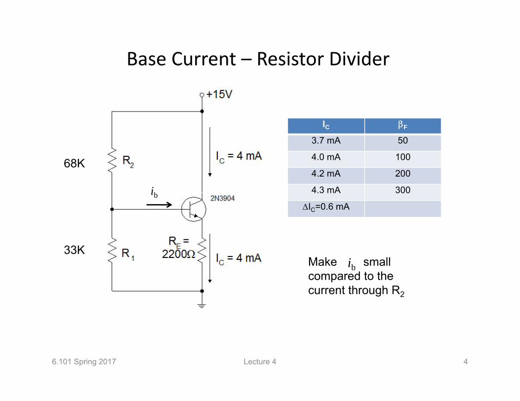
Base Current – Resistor Divider
6.101 Spring 2017 Lecture 4 4
68K
33K
IC F
3.7 mA 50
4.0 mA 100
4.2 mA 200
4.3 mA 300
IC=0.6 mAib
Make small compared to the current through R2
ib

Commom Emitter – Hybrid π
6.101 Spring 2017 Lecture 4 5
RB
+15V
2N3904
ICRL
C +
vout
_
IB
+
TRANSISTOR AMPLIFIER CONFIGURATIONS WITH HYBRID- EQUIVALENT CIRCUITS
Rs
+vin
_
Rs
r
RL
ib
+
vout
_
c
e
b
+vin
_
RB
COMMON EMITTER AMPLIFER
Lm
m
o
Lov
Lo
b
Lbo
in
outv
Rg
g
RAthen
rR
riRi
vvA
1
1
mvVVI
g
rg
THTH
CQm
m
26
0
vgv
m
outv1
inv1

Common Emitter with Emitter Degeneration
6.101 Spring 2017 Lecture 4 6
ELvEo
Eo
Lo
Eob
Lbo
in
outv
RRAthenRrif
RrR
RriRi
vvA
/;1
;111
1
• Input resistance (β+1)RE• Voltage gain reduced by (1+gm RE)• Voltage gain less dependent on β
(linearity)
outv1
inv1

AC Coupled vs DC Coupled Amplifiers• AC Coupling
– Advantage: easy cascading with DC blocking capacitor, bias stability and stage independent
– Disadvantage: lot’s of R’s and C’s, no DC gain, need large C for low freqency
• DC coupling– Some gain at DC– Fewer R’s C’s
6.101 Spring 2017 Lecture 4 7

Gain vs Frequency
6.101 Spring 2017 Lecture 4 8

Cutoff Frequency Analysis
6.101 Spring 2017 Lecture 4 9

Low Pass Filter LPF
6.101 Spring 2017 10
RV1 V2C
RCfcutofffrequencyHigh
sRCA
RCjCj
R
CjXjR
XjVVA
v
C
Cv
21
11
11
1
1
1
2
log f
AV (dB)
-3dB
fHI or f-3dB
slope = -6 dB / octaveslope = -20 dB / decade
0
log f
Degrees
-45o
fHI or f-3dB
0o
-90o
PHASE LAG
Lecture 2
log scale

Cutoff Frequency Analysis
6.101 Spring 2017 Lecture 4 11
3db f3db f 1
2RC 1
2 r (C C )
but 0 g m r or f g m
2 r (C C )
ib vbe
r vbe j (C C )
hfe gmvbe
ib gmr
1 j r (C C )
1 j r (C C )
h fe
1 j( ff
)ft hfe 1 or ft
g m
2 r (C C )

Cutoff Frequency Parameters
6.101 Spring 2017 Lecture 4 12
g mq
kT
IC
0 hfe (datasheet)C Cob (datasheet)
g m
2 (C C ) fT (transit frequency datasheet)
C g m
2 fTrC

6.101 Spring 2017 Lecture 4 13
β
Use max for worst case cu

Miller Effect* – Common Emitter
6.101 Spring 2017 Lecture 4 14
)](1[ LCmM RRgCC • Neamen, Microlectronics 3rd Edition p 514

Miller Effect
6.101 Spring 2017 Lecture 4 15
RC RC 4k r 2.6k RB 200kC 4pF C 0.2pF gm 38.5ma /V
f3db f 1
2 r ||RB (C C )15.5MHz
withMiller EffectCM C[1 gm (RC RL )]
f3db f 1
2 r ||RB (C CM )3.16MHz
*Neamen, Microlectronics 3rd Edition p 515

6.101 Spring 2017 Lecture 4 16
2N3904CE configuration, VCC +15v

Common Base Configuration
6.101 Spring 2017 Lecture 4 17

Common Collector (Emitter Follower)
6.101 Spring 2017 Lecture 4 18
• Buffer with unity gain• High input resistance driving low
output resistance (current gain).
mvVVI
g
rg
THTH
CQm
m
26
0
outv1inv1
1;1
;1'
11'
11
1
vEo
Eos
Eo
Eosb
Ebo
in
outv
AthenRrif
RrRR
RrRiRi
vvA

Common Collector – Emitter Follower Biasing
• Β = 100, iB = 7.5ma/100 =‐ 75µa• Using Thevenin equivalent,
RB = R1||R2, VB =
6.101 Spring 2017 Lecture 4 19
+15V
R 1
2N3904
7.5 mA
1.0 k7.5 mA
R2
A
B
7.5 V
2N3904
7.5 mA
+15V
VB
RB
IB
21
115RR
R
VB = IBRB + 0.6V + 7.5VVB = [75 µA x 10k] + 0.6V + 7.5VVB = 750 mV + 0.6V + 7.5VVB = 8.9V
[15 R1] ÷ [R1 + R2] = 8.9V15 R1 = 8.9 x [R1 + R2][15−8.9] R1 = 8.9 R2R1 = 1.44 R2[R1 x R2] ÷ [R1 + R2] = 10 kΩ
[1.44R2 x R2] ÷ [1.44 R2 + R2] = 10kΩR2 = 16.9 kΩ (use 16 kΩ)R1 = 1.44 R2 = 24.4 kΩ (use 24 kΩ)
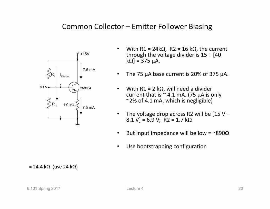
Common Collector – Emitter Follower Biasing
• With R1 = 24kΩ, R2 = 16 kΩ, the current through the voltage divider is 15 ÷ [40 kΩ] = 375 µA.
• The 75 µA base current is 20% of 375 µA.
• With R1 = 2 kΩ, will need a divider current that is ~ 4.1 mA. (75 µA is only ~2% of 4.1 mA, which is negligible)
• The voltage drop across R2 will be [15 V –8.1 V] = 6.9 V; R2 = 1.7 kΩ
• But input impedance will be low = ~890Ω
• Use bootstrapping configuration
6.101 Spring 2017 Lecture 4 20
= 24.4 kΩ (use 24 kΩ)
+15V
R 1
2N3904
7.5 mA
8.1 V
1.0 k7.5 mA
R2
A
B
IDivider

Low Frequency Hybrid‐ Equation Chart
6.101 Spring 2017 Lecture 4 21
High gain, better high frequency responseLow input resistance
Unity gain, low output resistanceHigh input resist.
High gain applicationsModerate input resistance
High output resistance

Introduction to LTspice
6.101 Spring 2017 Lecture 4 22
Acknowledgment: LTspice material based in part by Devon Rosner (6.101 TA), Engineer, Linear Technology


![BJT Circuits Limitations LTspiceTransistor Configurations 6.101 Spring 2020 Lecture 4 3 +15V + V in V OUT-R L R 1 + + R 2 [a] Common Emitter Amplifier [b] Common Collector [Emitter](https://img.dokumen.tips/doc/110x75/5fb86d5b50c3f54786723a2e/bjt-circuits-limitations-ltspice-transistor-configurations-6101-spring-2020-lecture.jpg)