Embed Size (px)
Citation preview

An IMPORTANT NOTICE at the end of this TI reference design addresses authorized use, intellectual property matters and other important disclaimers and information.
TINA-TI is a trademark of Texas Instruments WEBENCH is a registered trademark of Texas Instruments
SLAU525-June 2013-Revised June 2013 Bipolar +/-10V Analog Output from a Unipolar Voltage Output DAC 1 Copyright © 2013, Texas Instruments Incorporated
Kevin Duke
TI Precision Designs: Verified Design
Bipolar +/-10V Analog Output from a Unipolar Voltage Output DAC
TI Precision Designs Circuit Description
TI Precision Designs are analog solutions created by TI’s analog experts. Verified Designs offer the theory, component selection, simulation, complete PCB schematic & layout, bill of materials, and measured performance of useful circuits. Circuit modifications that help to meet alternate design goals are also discussed.
This unipolar to bipolar signal conditioning circuit uses an op amp with negative feedback and three resistors in a modified summing amplifier configuration to generate high-voltage bipolar outputs from a generic single supply unipolar digital-to-analog converter (DAC). This design will take consideration for generating voltage outputs commonly used in industrial process control applications and for driving reactive loads such as long cables also common in industrial applications. The fundamentals of the design can be extended to condition any unipolar DAC to any bipolar range of operation.
Design Resources
Design Archive All Design files TINA-TI™ SPICE Simulator DAC8560 Product Folder OPA188 Product Folder
Ask The Analog Experts WEBENCH® Design Center TI Precision Designs Library
DAC +
RFB
RG1
RG2
VREF
VOUT
www.ti.com
2 Bipolar +/-10V Analog Output from a Unipolar Voltage Output DAC SLAU525-June 2013-Revised June 2013 Copyright © 2013, Texas Instruments Incorporated
1 Design Summary
The design requirements are as follows:
DAC Supply Voltage: +5 V dc
Amplifier Supply Voltage: ±15 V dc
Input: 3-wire, 24-bit SPI
Output: ±10 V dc
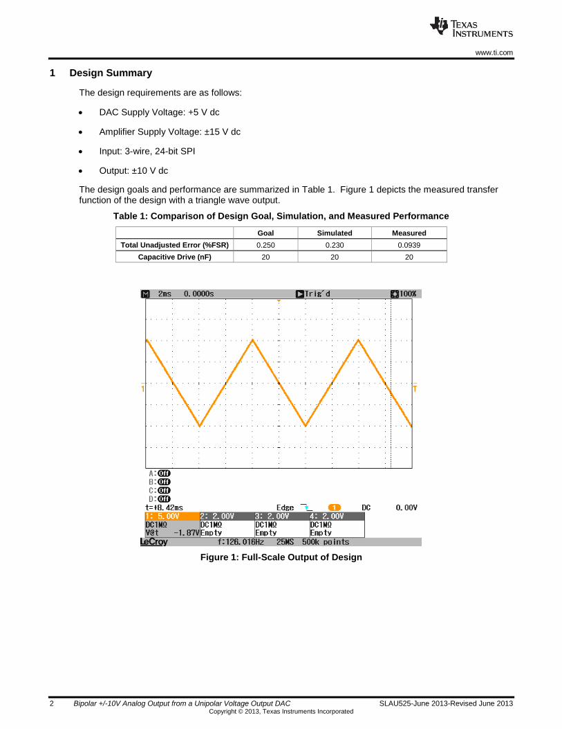
The design goals and performance are summarized in Table 1. Figure 1 depicts the measured transfer function of the design with a triangle wave output.
Table 1: Comparison of Design Goal, Simulation, and Measured Performance
Goal Simulated Measured
Total Unadjusted Error (%FSR) 0.250 0.230 0.0939
Capacitive Drive (nF) 20 20 20
Figure 1: Full-Scale Output of Design

www.ti.com
SLAU525-June 2013-Revised June 2013 Bipolar +/-10V Analog Output from a Unipolar Voltage Output DAC 3 Copyright © 2013, Texas Instruments Incorporated
2 Theory of Operation
A more complete schematic for this design, including capacitive load compensation, is shown in Figure 2. The dc transfer function is based on the ratio of the feedback resistor RFB and gain setting resistors RG1 and RG2.
+
RFBRG1
RG2
RISO
CCOMPVREF
VOUT
CLOADDAC8560
OPA188
Figure 2: Complete Circuit Schematic
The dc transfer function for this design is defined as:
REF
G
FBDAC
G
FB
G
FBOUT V
R
RV
R
R
R
RV
212
1
(1)
2.1 Choosing Resistor Values
The amplifier in this circuit uses negative feedback to ensure that the voltage at the inverting and non-inverting terminals are equal. When the DAC output is at zero-scale (0 V) the inverting terminal is a virtual ground so no current will flow across RG1, this causes the circuit to function as an inverting amplifier with gain equal to RFB / RG2. When the DAC output is full-scale (VREF) the inverting terminal potential is equal to VREF so no current will flow across RG2, this causes the circuit to function as a non-inverting amplifier with gain equal to (1 + RFB / RG1).
A simple three-step process can be used to select the resistor values used to realize any bipolar output range using any generic unipolar DAC. For this design VREF was selected to be 2.5 V, a very common internal reference value for a generic DAC and a readily available external reference value. The desired output range for this design is ±10 V.
First, using the transfer function shown in Equation 1, consider the negative full-scale output case when VDAC is equal to 0 V, VREF is equal to 2.5 V, and VOUT is equal to -10 V. This case is used to calculate the ratio of RFB to RG2 and is shown explicitly in Equation 2.
VR
R
R
R
R
RV
G
FB
G
FB
G
FB 5.20110212
(2)
VR
RV
G
FB 5.2102
2*4 GFB RR
www.ti.com
4 Bipolar +/-10V Analog Output from a Unipolar Voltage Output DAC SLAU525-June 2013-Revised June 2013 Copyright © 2013, Texas Instruments Incorporated
Second, consider the positive full-scale output case when VDAC is equal to 2.5 V, VREF is equal to 2.5 V, and VOUT is equal to 10 V. This case is used to calculate the ratio of RFB to RG1 and is shown explicitly in Equation 3.
VR
R
R
R
R
RV
G
FB
G
FB
G
FB 5.25.2110212
(3)
VR
RV
G
FB 5.21101
31
FBG
RR
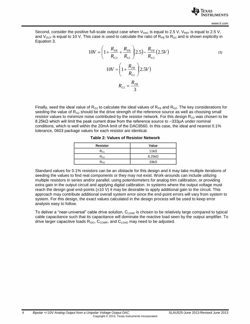
Finally, seed the ideal value of RG2 to calculate the ideal values of RFB and RG2. The key considerations for seeding the value of RG2 should be the drive strength of the reference source as well as choosing small resistor values to minimize noise contributed by the resistor network. For this design RG2 was chosen to be 8.25kΩ which will limit the peak current draw from the reference source to ~333µA under nominal conditions, which is well within the 20mA limit of the DAC8560. In this case, the ideal and nearest 0.1% tolerance, 0603 package values for each resistor are identical.
Table 2: Values of Resistor Network
Resistor Value
RG1 11kΩ
RG2 8.25kΩ
RFB 33kΩ
Standard values for 0.1% resistors can be an obstacle for this design and it may take multiple iterations of seeding the values to find real components or they may not exist. Work-arounds can include utilizing multiple resistors in series and/or parallel, using potentiometers for analog trim calibration, or providing extra gain in the output circuit and applying digital calibration. In systems where the output voltage must reach the design goal end-points (±10 V) it may be desirable to apply additional gain to the circuit. This approach may contribute additional overall system error since the end-point errors will vary from system to system. For this design, the exact values calculated in the design process will be used to keep error analysis easy to follow.
To deliver a “near-universal” cable drive solution, CLOAD is chosen to be relatively large compared to typical cable capacitance such that its capacitance will dominate the reactive load seen by the output amplifier. To drive larger capacitive loads RISO, CCOMP, and CLOAD may need to be adjusted.
www.ti.com
SLAU525-June 2013-Revised June 2013 Bipolar +/-10V Analog Output from a Unipolar Voltage Output DAC 5 Copyright © 2013, Texas Instruments Incorporated
3 Component Selection
3.1 DAC Selection
For convenience, devices with an external reference option or devices with accessible internal references are desirable in this application since the reference is used to create an offset. The DAC selection in this design should primarily be based on dc error contributions typically described by offset-error, gain-error, and integral non-linearity error. Occasionally additional specifications are provided that summarize end-point errors of the DAC typically called zero-code error and full-scale error. For ac applications additional consideration may be placed on slew rate and settling time.
3.2 Amplifier Selection
Amplifier input offset voltage (VOS) is a key-consideration for this design. VOS of an operational amplifier is a typical datasheet specification but in-circuit performance is also impacted by drift over temperature, the common-mode rejection ratio (CMRR), and power supply rejection ratio (PSRR) so consideration should be given to these parameters as well. For ac operation additional considerations should be made concerning slew rate and settling time. Input-bias current (IB) can also be a factor, but typically the resistor network is implemented with sufficiently small resistor values that the effects of input-bias current are negligible.
3.3 Passive Component Selection
Resistor matching for the op amp resistor network is critical for the success of this design and components should be chosen with tight tolerances. For this design 0.1% resistor values are implemented but this constraint may be adjusted based on application specific design goals. Resistor matching will contribute to both offset error and gain error in this design, as shown in the simulation section of this document. The tolerance of stability components RISO and CCOMP is not critical and 1% components are acceptable.
www.ti.com
6 Bipolar +/-10V Analog Output from a Unipolar Voltage Output DAC SLAU525-June 2013-Revised June 2013 Copyright © 2013, Texas Instruments Incorporated
4 Simulation
4.1 DAC DC Transfer Function
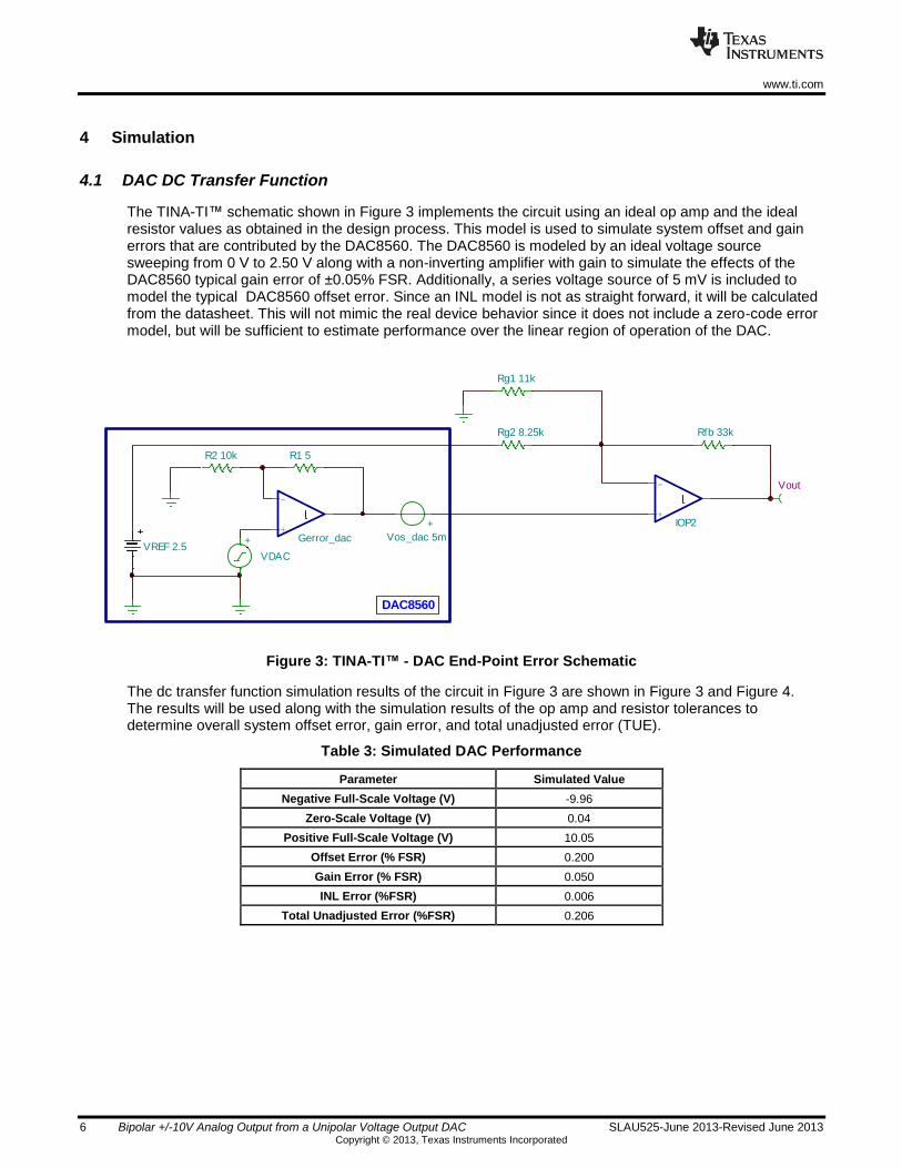
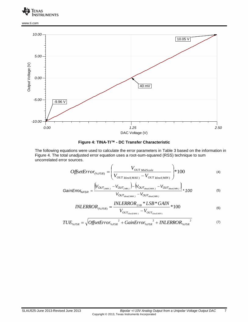
The TINA-TI™ schematic shown in Figure 3 implements the circuit using an ideal op amp and the ideal resistor values as obtained in the design process. This model is used to simulate system offset and gain errors that are contributed by the DAC8560. The DAC8560 is modeled by an ideal voltage source sweeping from 0 V to 2.50 V along with a non-inverting amplifier with gain to simulate the effects of the DAC8560 typical gain error of ±0.05% FSR. Additionally, a series voltage source of 5 mV is included to model the typical DAC8560 offset error. Since an INL model is not as straight forward, it will be calculated from the datasheet. This will not mimic the real device behavior since it does not include a zero-code error model, but will be sufficient to estimate performance over the linear region of operation of the DAC.
-
+Gerror_dac+
VDAC
R1 5R2 10k
-
+IOP2
Rfb 33kRg2 8.25k
Vout
Rg1 11k
VREF 2.5
+
Vos_dac 5m
DAC8560
Figure 3: TINA-TI™ - DAC End-Point Error Schematic
The dc transfer function simulation results of the circuit in Figure 3 are shown in Figure 3 and Figure 4. The results will be used along with the simulation results of the op amp and resistor tolerances to determine overall system offset error, gain error, and total unadjusted error (TUE).
Table 3: Simulated DAC Performance
Parameter Simulated Value
Negative Full-Scale Voltage (V) -9.96
Zero-Scale Voltage (V) 0.04
Positive Full-Scale Voltage (V) 10.05
Offset Error (% FSR) 0.200
Gain Error (% FSR) 0.050
INL Error (%FSR) 0.006
Total Unadjusted Error (%FSR) 0.206
www.ti.com
SLAU525-June 2013-Revised June 2013 Bipolar +/-10V Analog Output from a Unipolar Voltage Output DAC 7 Copyright © 2013, Texas Instruments Incorporated
10.05 V
-9.96 V
40 mV
DAC Voltage (V)
0.00 1.25 2.50
Ou
tpu
t V
olta
ge
(V
)
-10.00
-5.00
0.00
5.00
10.00
40 mV
-9.96 V
10.05 V
Figure 4: TINA-TI™ - DC Transfer Characteristic
The following equations were used to calculate the error parameters in Table 3 based on the information in Figure 4. The total unadjusted error equation uses a root-sum-squared (RSS) technique to sum uncorrelated error sources.
100*)()(
)(%
MINIdealOUTMAXIdealOUT
MidScaleOUT
FSRVV
VrOffsetErro (4)
100*
VV
VVVVGainError
)MIN(Ideal)MAX(Ideal
)MIN(Ideal)MAX(Ideal)MIN()MAX(
OUTOUT
OUTOUTOUTOUT
FSR%
(5)
100***
)()(
)(%
MINIdealMAXIdeal OUTOUT
LSB
FSRVV
GAINLSBINLERRORINLERROR
(6)
2
%
2
%
2
%% FSRFSRFSRFSR INLERRORGainErrorrOffsetErroTUE (7)

www.ti.com
8 Bipolar +/-10V Analog Output from a Unipolar Voltage Output DAC SLAU525-June 2013-Revised June 2013 Copyright © 2013, Texas Instruments Incorporated
4.2 Op Amp & Passives DC Transfer Function
The TINA-TI™ schematic shown in Figure 5 implements the OPA188 model and Monte-Carlo analysis for the resistor network with 0.1% tolerances and a normal distribution. In this simulation the DAC will be represented by an ideal voltage source sweeping from 0 V to 2.5 V. This model is used to simulate the offset error and gain error contributed by the resistors and op amp. The Monte Carlo dc transfer function is depicted in Figure 6.
VCC
VSS
VSS
VCC
V1 15
C1 1
u
V2 -15
C2 1
u VREF 2.5
+
VDAC
C4 100p
C5 100n
C6 100p
C7 100n
RFB 33kRG2 11k
RG1 8.25k
VOUT-
++V
U1 OPA188
Clo
ad 2
0n
Riso 70
Ccomp 150p
Figure 5: TINA-TI™ - DC Transfer Characteristic
VOUT[9]
DAC Voltage (V)
0.00 1.25 2.50
Ou
tpu
t V
olta
ge
(V
)
-20.00
-10.00
0.00
10.00
20.00
VOUT[9]
VOUT[1] A:(1.25; -107.339128u)
VOUT[2] A:(1.25; 684.300937u)
VOUT[3] A:(1.25; -448.4154u)
VOUT[4] A:(1.25; 107.987098u)
VOUT[5] A:(1.25; -786.022041u)
VOUT[6] A:(1.25; -1.738254m)
VOUT[7] A:(1.25; -969.044351u)
VOUT[8] A:(1.25; -443.762704u)
VOUT[9] A:(1.25; -56.172436u)
VOUT[10] A:(1.25; 1.785828m)
VOUT[1] A:(2.5; 9.994267)
VOUT[2] A:(2.5; 10.005706)
VOUT[3] A:(2.5; 9.999384)
VOUT[4] A:(2.5; 10.000151)
VOUT[5] A:(2.5; 10.000798)
VOUT[6] A:(2.5; 9.999518)
VOUT[7] A:(2.5; 9.999575)
VOUT[8] A:(2.5; 10.001931)
VOUT[9] A:(2.5; 9.996543)
VOUT[10] A:(2.5; 9.996942)
VOUT[1] A:(0; -9.994482)
VOUT[2] A:(0; -10.004337)
VOUT[3] A:(0; -10.00028)
VOUT[4] A:(0; -9.999935)
VOUT[5] A:(0; -10.00237)
VOUT[6] A:(0; -10.002995)
VOUT[7] A:(0; -10.001513)
VOUT[8] A:(0; -10.002818)
VOUT[9] A:(0; -9.996655)
VOUT[10] A:(0; -9.99337)
Figure 6: TINA-TI™ - Monte-Carlo Simulation of Output Circuit
www.ti.com
SLAU525-June 2013-Revised June 2013 Bipolar +/-10V Analog Output from a Unipolar Voltage Output DAC 9 Copyright © 2013, Texas Instruments Incorporated
The results of a 10 iteration Monte-Carlo simulation of the output circuit are shown in Table 4.
Table 4: Output Circuit Monte-Carlo Results
Min Max Average Std. Dev. (σ)
Offset Error (mV) -1.738 1.785 -0.197 0.958
Full-Scale Range (V) 19.988 20.010 19.999 0.006
Full-Scale |Error| (mV) 0.086 11.251 4.972 N/A
The standard deviation of the Monte-Carlo results can be used to generate a more realistic error figure for the system by multiplying the standard deviation by 3, commonly referred to as a 3-σ system. This error figure should encompass 99.7% of the systems, leaving out absolute worst-case resistor mis-matches that are highly unlikely to occur. These errors are summarized in Table 5. The equations used to calculate each error are shown below:
100**3
)()(
)(%
MINIdealMAXIdeal OUTOUT
rOffsetErro
FSRVV
rOffsetErro
( 8 )
100**3
)()(
)(%
MINIdealMAXIdeal OUTOUT
GainError
FSRVV
GainError
(9)
Table 5: Simulated Output Circuit Performance
Parameter Simulated Value
Offset Error (% FSR) 0.0143
Gain Error (% FSR) 0.1004
INL Error (%FSR) 0.0000
Total Unadjusted Error (%FSR) 0.1014
4.3 System dc Transfer Function
The combined accuracy of simulation results of the DAC and output circuit are summarized in Table 6. The values were calculated using a RSS technique similar to that shown in Equation 7. The output circuit contributes very low error to the system which allows for the DACs performance to dominate what is seen at the output. In this case the DAC errors are gained up by 8 since the 0-2.5 V range was scaled up to ±10 V. If less gain is applied to the DAC output signal its error contributions will decrease.
Table 6: Simulated Circuit Performance
Parameter Simulated Value
Offset Error (% FSR) 0.200
Gain Error (% FSR) 0.112
INL Error (%FSR) 0.012
Total Unadjusted Error (%FSR) 0.230

www.ti.com
10 Bipolar +/-10V Analog Output from a Unipolar Voltage Output DAC SLAU525-June 2013-Revised June 2013 Copyright © 2013, Texas Instruments Incorporated
4.4 Step Response
The step response of the design is shown in Figure 7. The results show that the output settles to the proper value with very little overshoot and ringing while driving the 20nF CLOAD, indicating a stable design. The stable response was obtained by manipulating the compensation components, RISO and CCOMP. See Reference 1 more information on stability.
Time (s)
0.00 25.00u 50.00u
Ou
tpu
t V
olta
ge
(V
)
6.00
6.05
6.10
6.15
6.20
Figure 7: TINA-TI™ - Step Response
www.ti.com
SLAU525-June 2013-Revised June 2013 Bipolar +/-10V Analog Output from a Unipolar Voltage Output DAC 11 Copyright © 2013, Texas Instruments Incorporated
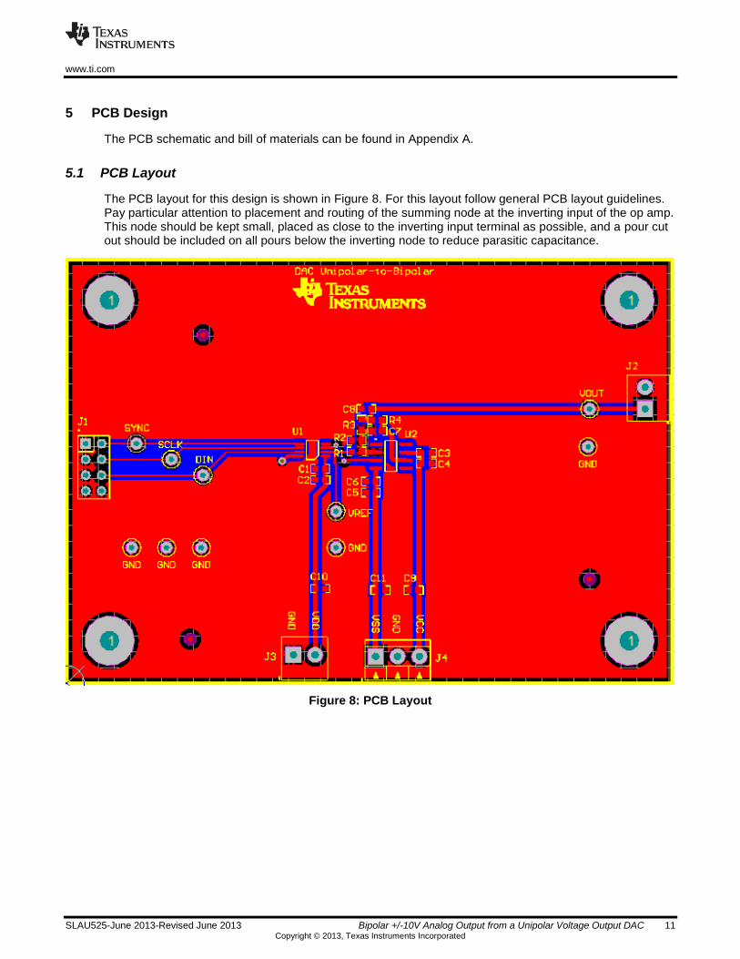
5 PCB Design
The PCB schematic and bill of materials can be found in Appendix A.
5.1 PCB Layout
The PCB layout for this design is shown in Figure 8. For this layout follow general PCB layout guidelines. Pay particular attention to placement and routing of the summing node at the inverting input of the op amp. This node should be kept small, placed as close to the inverting input terminal as possible, and a pour cut out should be included on all pours below the inverting node to reduce parasitic capacitance.
Figure 8: PCB Layout
www.ti.com
12 Bipolar +/-10V Analog Output from a Unipolar Voltage Output DAC SLAU525-June 2013-Revised June 2013 Copyright © 2013, Texas Instruments Incorporated
6 Verification & Measured Performance
6.1 Transfer Function
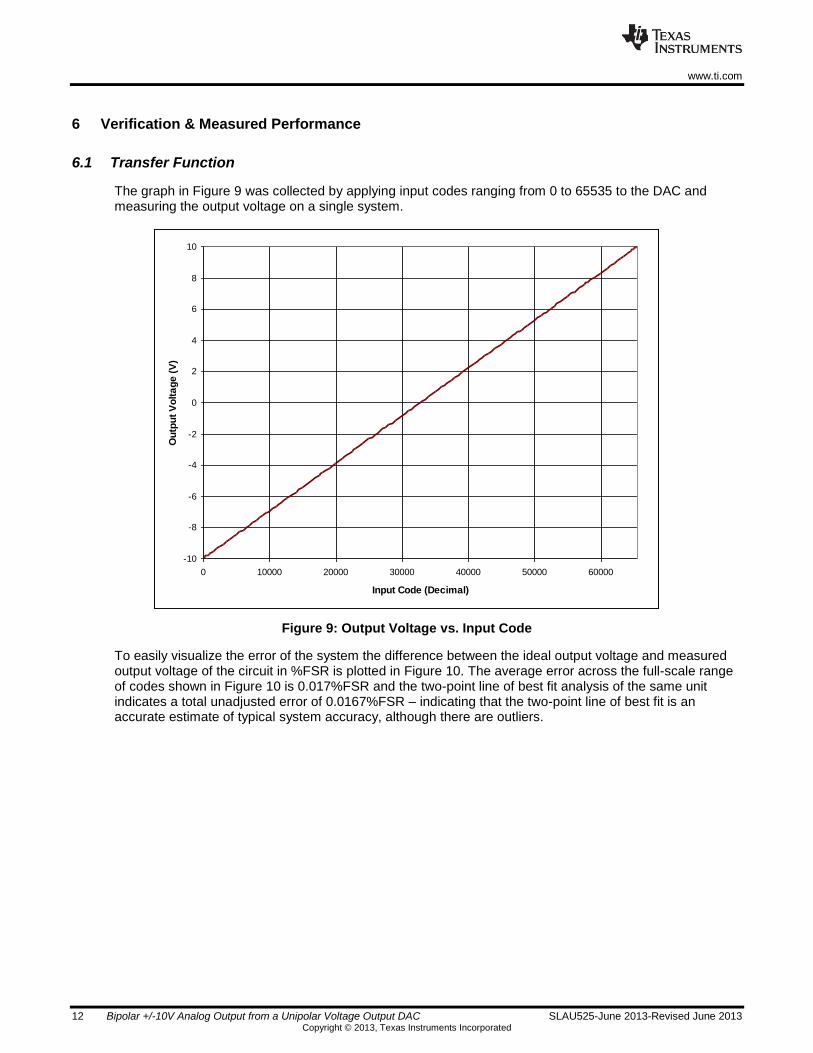
The graph in Figure 9 was collected by applying input codes ranging from 0 to 65535 to the DAC and measuring the output voltage on a single system.
-10
-8
-6
-4
-2
0
2
4
6
8
10
0 10000 20000 30000 40000 50000 60000
Input Code (Decimal)
Ou
tpu
t V
olt
ag
e (
V)
Figure 9: Output Voltage vs. Input Code
To easily visualize the error of the system the difference between the ideal output voltage and measured output voltage of the circuit in %FSR is plotted in Figure 10. The average error across the full-scale range of codes shown in Figure 10 is 0.017%FSR and the two-point line of best fit analysis of the same unit indicates a total unadjusted error of 0.0167%FSR – indicating that the two-point line of best fit is an accurate estimate of typical system accuracy, although there are outliers.

www.ti.com
SLAU525-June 2013-Revised June 2013 Bipolar +/-10V Analog Output from a Unipolar Voltage Output DAC 13 Copyright © 2013, Texas Instruments Incorporated
0
0.005
0.01
0.015
0.02
0.025
0.03
0.035
0.04
0 10000 20000 30000 40000 50000 60000
Input Code (Decimal)
Ou
tpu
t E
rro
r (%
FS
R)
Figure 10: Output Voltage Error vs. Input Code
The average results observed over 8 units are shown in Table 7. These results were measured using a two-point line of best fit measured at codes 485 and 64714 to be consistent with the specifications provided in the DAC8560 datasheet. The equations used to calculate these values are shown in Equations 10 and 11.
Table 7: Measured Circuit Performance
Parameter Measured Value
Offset Error (% FSR) 0.0705
Gain Error (% FSR) 0.0125
INL Error (%FSR) 0.0060
Total Unadjusted Error (%FSR) 0.0939
100*
)485()64714(
)485()64714()485()64714(
)(%
IDEALIDEAL
IDEALIDEALREALREAL
OUTOUT
OUTOUTOUTOUT
FSRVV
VVVVGainError
(10)
100*
10485*48564714
)()(
)485()64714(
)485(
)(%
MINIDEALMAXIDEAL
REALREAL
REAL
OUTOUT
OUTOUT
OUT
FSRVV
VVV
rOffsetErro
(11)
www.ti.com
14 Bipolar +/-10V Analog Output from a Unipolar Voltage Output DAC SLAU525-June 2013-Revised June 2013 Copyright © 2013, Texas Instruments Incorporated
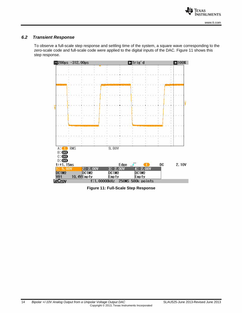
6.2 Transient Response
To observe a full-scale step response and settling time of the system, a square wave corresponding to the zero-scale code and full-scale code were applied to the digital inputs of the DAC. Figure 11 shows this step response.
Figure 11: Full-Scale Step Response
www.ti.com
SLAU525-June 2013-Revised June 2013 Bipolar +/-10V Analog Output from a Unipolar Voltage Output DAC 15 Copyright © 2013, Texas Instruments Incorporated
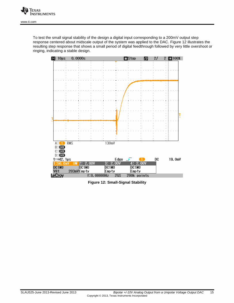
To test the small signal stability of the design a digital input corresponding to a 200mV output step response centered about midscale output of the system was applied to the DAC. Figure 12 illustrates the resulting step response that shows a small period of digital feedthrough followed by very little overshoot or ringing, indicating a stable design.
Figure 12: Small-Signal Stability

www.ti.com
16 Bipolar +/-10V Analog Output from a Unipolar Voltage Output DAC SLAU525-June 2013-Revised June 2013 Copyright © 2013, Texas Instruments Incorporated
7 Modifications
The components selected in this design were chosen based on the design goals outlined at the beginning of this document. The DAC selection can be very open since the output circuit is applicable to any device and should be made based on specific design goals. Alternative DACs may provide enhanced linearity, gain error, and offset error as well as alternative interface options, channel count, resolution, and other auxiliary features. Table 7 shows a few DACs that may be used in place of the DAC8560.
Modifications to improve the accuracy of this design are possible by choosing a more precise DAC and by utilizing an external reference source. For this design, delivering a very low-cost solution was a critical parameter and some sacrifices were made. Additionally, the implementation of external calibration can greatly enhance results.
Table 8: Alternate DAC Options
DAC Gain Error (Typ) Offset Error
(Typ) INL Error (Typ) Resolution Channel Count
DAC8560 ±0.05 %FSR ±5 mV ±8 LSB 16 bits 1
DAC8562/3 ±0.01 %FSR ±1 mV ±4 LSB 16 bits 2
DAC8564 ±0.05 %FSR ±5 mV ±4 LSB 16 bits 4
DAC8568 ±0.01 %FSR ±1 mV ±4 LSB 16 bits 8
DAC8411 ±0.05 %FSR ±0.05 mV ±1 LSB 16 bits 1
DAC8881 ±4 LSB ±4 LSB ±0.5 LSB 16 bits 1
The OPA188 is an excellent wide-supply amplifier with very low input offset voltage and input offset voltage drift due to its chopper topology. Other op amps may be selected that offer lower noise, zero cross-over distortion, or higher bandwidth. Designs that deliver a smaller output range have many more options available since the supply voltage requirements are lowered.
Table 9: Alternate Op Amp Options
Amplifier Max Supply
Voltage Offset Voltage
(Typ) Offset Drift (Typ) Bandwidth
Quiescent Current
OPA180 36 V 15 µV 0.1 µV/C 2 MHz 450 µA
OPA188 36 V 6 µV 0.085 µV/C 2 MHz 450 µA
OPA170 36 V 0.25 mV 0.3 µV/C 1.2 MHz 110 µA
OPA211 36 V 30 µV 0.35 µV/C 80 MHz 3.6 µA
OPA227 36 V 10 µV 0.1 µV/C 1 MHz 790 µA
OPA140 36 V 30 µV 0.35 µV/C 11 MHz 1.8 mA
OPA277 36 V 10 µV 0.1 µV/C 1 MHz 790 µA
8 About the Author
Kevin Duke is an applications engineer in the precision digital to analog converters group at Texas Instruments where he supports industrial and catalog products and applications. Kevin received his BSEE from Texas Tech University in 2010.

www.ti.com
SLAU525-June 2013-Revised June 2013 Bipolar +/-10V Analog Output from a Unipolar Voltage Output DAC 17 Copyright © 2013, Texas Instruments Incorporated
9 Acknowledgements & References
1. T. Green (2012). Operational Amplifier Stability, Part 10 of 15: Capacitor Loop Stability: Riso with Dual Feedback. Available: http://www.en-genius.net/site/zones/acquisitionZONE/technical_notes/acqt_050712
www.ti.com
18 Bipolar +/-10V Analog Output from a Unipolar Voltage Output DAC SLAU525-June 2013-Revised June 2013 Copyright © 2013, Texas Instruments Incorporated
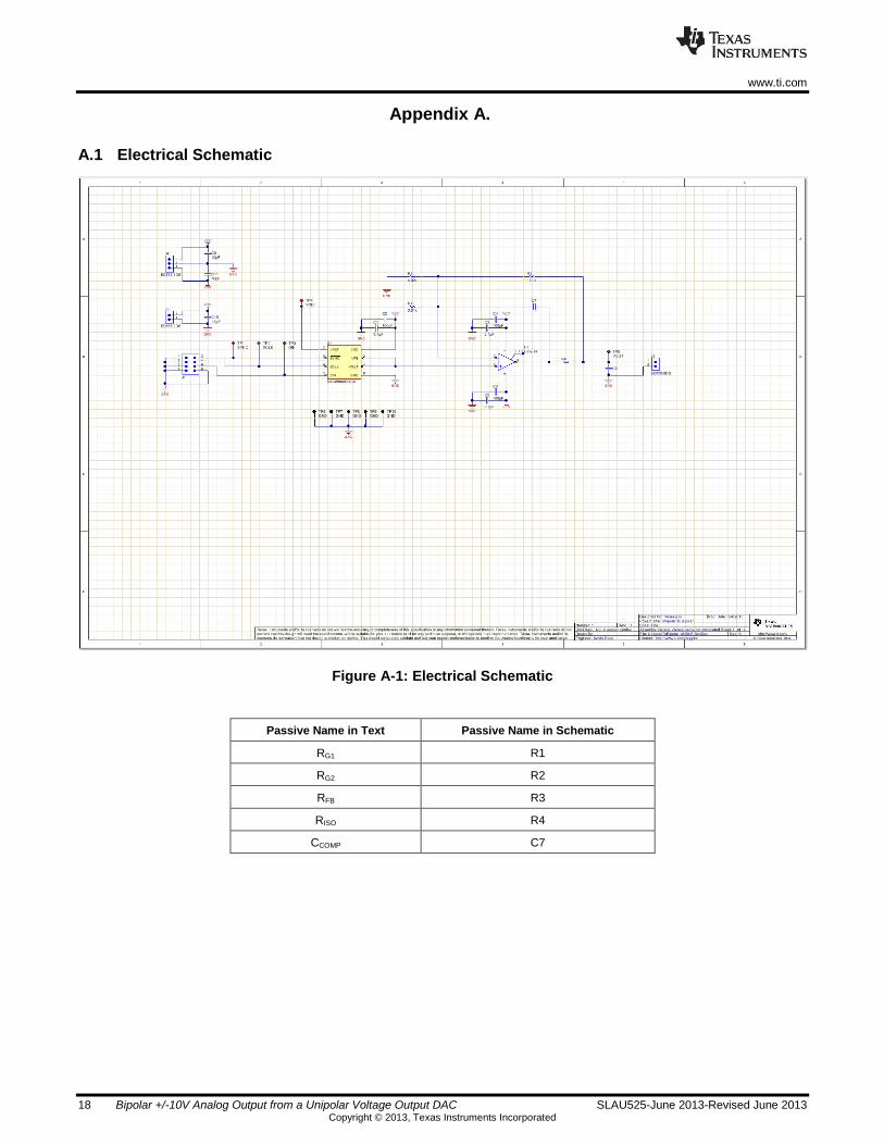
Appendix A.
A.1 Electrical Schematic
Figure A-1: Electrical Schematic
Passive Name in Text Passive Name in Schematic
RG1 R1
RG2 R2
RFB R3
RISO R4
CCOMP C7

www.ti.com
SLAU525-June 2013-Revised June 2013 Bipolar +/-10V Analog Output from a Unipolar Voltage Output DAC 19 Copyright © 2013, Texas Instruments Incorporated
A.2 Bill of Materials
Figure A-2: Bill of Materials
IMPORTANT NOTICE FOR TI REFERENCE DESIGNSTexas Instruments Incorporated ("TI") reference designs are solely intended to assist designers (“Buyers”) who are developing systems thatincorporate TI semiconductor products (also referred to herein as “components”). Buyer understands and agrees that Buyer remainsresponsible for using its independent analysis, evaluation and judgment in designing Buyer’s systems and products.TI reference designs have been created using standard laboratory conditions and engineering practices. TI has not conducted anytesting other than that specifically described in the published documentation for a particular reference design. TI may makecorrections, enhancements, improvements and other changes to its reference designs.Buyers are authorized to use TI reference designs with the TI component(s) identified in each particular reference design and to modify thereference design in the development of their end products. HOWEVER, NO OTHER LICENSE, EXPRESS OR IMPLIED, BY ESTOPPELOR OTHERWISE TO ANY OTHER TI INTELLECTUAL PROPERTY RIGHT, AND NO LICENSE TO ANY THIRD PARTY TECHNOLOGYOR INTELLECTUAL PROPERTY RIGHT, IS GRANTED HEREIN, including but not limited to any patent right, copyright, mask work right,or other intellectual property right relating to any combination, machine, or process in which TI components or services are used.Information published by TI regarding third-party products or services does not constitute a license to use such products or services, or awarranty or endorsement thereof. Use of such information may require a license from a third party under the patents or other intellectualproperty of the third party, or a license from TI under the patents or other intellectual property of TI.TI REFERENCE DESIGNS ARE PROVIDED "AS IS". TI MAKES NO WARRANTIES OR REPRESENTATIONS WITH REGARD TO THEREFERENCE DESIGNS OR USE OF THE REFERENCE DESIGNS, EXPRESS, IMPLIED OR STATUTORY, INCLUDING ACCURACY ORCOMPLETENESS. TI DISCLAIMS ANY WARRANTY OF TITLE AND ANY IMPLIED WARRANTIES OF MERCHANTABILITY, FITNESSFOR A PARTICULAR PURPOSE, QUIET ENJOYMENT, QUIET POSSESSION, AND NON-INFRINGEMENT OF ANY THIRD PARTYINTELLECTUAL PROPERTY RIGHTS WITH REGARD TO TI REFERENCE DESIGNS OR USE THEREOF. TI SHALL NOT BE LIABLEFOR AND SHALL NOT DEFEND OR INDEMNIFY BUYERS AGAINST ANY THIRD PARTY INFRINGEMENT CLAIM THAT RELATES TOOR IS BASED ON A COMBINATION OF COMPONENTS PROVIDED IN A TI REFERENCE DESIGN. IN NO EVENT SHALL TI BELIABLE FOR ANY ACTUAL, SPECIAL, INCIDENTAL, CONSEQUENTIAL OR INDIRECT DAMAGES, HOWEVER CAUSED, ON ANYTHEORY OF LIABILITY AND WHETHER OR NOT TI HAS BEEN ADVISED OF THE POSSIBILITY OF SUCH DAMAGES, ARISING INANY WAY OUT OF TI REFERENCE DESIGNS OR BUYER’S USE OF TI REFERENCE DESIGNS.TI reserves the right to make corrections, enhancements, improvements and other changes to its semiconductor products and services perJESD46, latest issue, and to discontinue any product or service per JESD48, latest issue. Buyers should obtain the latest relevantinformation before placing orders and should verify that such information is current and complete. All semiconductor products are soldsubject to TI’s terms and conditions of sale supplied at the time of order acknowledgment.TI warrants performance of its components to the specifications applicable at the time of sale, in accordance with the warranty in TI’s termsand conditions of sale of semiconductor products. Testing and other quality control techniques for TI components are used to the extent TIdeems necessary to support this warranty. Except where mandated by applicable law, testing of all parameters of each component is notnecessarily performed.TI assumes no liability for applications assistance or the design of Buyers’ products. Buyers are responsible for their products andapplications using TI components. To minimize the risks associated with Buyers’ products and applications, Buyers should provideadequate design and operating safeguards.Reproduction of significant portions of TI information in TI data books, data sheets or reference designs is permissible only if reproduction iswithout alteration and is accompanied by all associated warranties, conditions, limitations, and notices. TI is not responsible or liable forsuch altered documentation. Information of third parties may be subject to additional restrictions.Buyer acknowledges and agrees that it is solely responsible for compliance with all legal, regulatory and safety-related requirementsconcerning its products, and any use of TI components in its applications, notwithstanding any applications-related information or supportthat may be provided by TI. Buyer represents and agrees that it has all the necessary expertise to create and implement safeguards thatanticipate dangerous failures, monitor failures and their consequences, lessen the likelihood of dangerous failures and take appropriateremedial actions. Buyer will fully indemnify TI and its representatives against any damages arising out of the use of any TI components inBuyer’s safety-critical applications.In some cases, TI components may be promoted specifically to facilitate safety-related applications. With such components, TI’s goal is tohelp enable customers to design and create their own end-product solutions that meet applicable functional safety standards andrequirements. Nonetheless, such components are subject to these terms.No TI components are authorized for use in FDA Class III (or similar life-critical medical equipment) unless authorized officers of the partieshave executed an agreement specifically governing such use.Only those TI components that TI has specifically designated as military grade or “enhanced plastic” are designed and intended for use inmilitary/aerospace applications or environments. Buyer acknowledges and agrees that any military or aerospace use of TI components thathave not been so designated is solely at Buyer's risk, and Buyer is solely responsible for compliance with all legal and regulatoryrequirements in connection with such use.TI has specifically designated certain components as meeting ISO/TS16949 requirements, mainly for automotive use. In any case of use ofnon-designated products, TI will not be responsible for any failure to meet ISO/TS16949.
Mailing Address: Texas Instruments, Post Office Box 655303, Dallas, Texas 75265Copyright © 2014, Texas Instruments Incorporated