Embed Size (px)
Citation preview

Bionics Chemical Synapse
by
Surachoke Thanapitak
December 2011
A thesis submitted forthe degree of Doctor of Philosophy of Imperial College London
Department of Electrical and Electronic EngineeringImperial College of Science, Technology and Medicine

Acknowledgements
First of all, I would like to express my gratitude to Professor Chris Toumazou who has
been my supervisor for the past five years, ever since I was an MSc student in 2006.
Without his support and encouragement, this work would not have reached a successful
conclusion. Professor Toumazou not only inspired my interest in analogue circuit design
but he has also enlightened me to understand how important it is especially in the field
of bionics.
Secondly, I am grateful to my fellow researchers at the Centre of Bio-inspired Technol-
ogy and other groups, including Dr. Panavy Pookaiyaudom, Dr. Thanut Tosanguan,
Jakgrarath Leenutaphong, Yan Liu, Abdul Al-ahdal, Achirapa Bandhaya, Jackravut
Dejvises, Supattra Visessri, Soratos Tantideeravit, Sasinee Bunyarataphan and Parinya
Seelanan. Also, I would like to thanks Dr. Timothy Constandinou, Dr. Pantelis Geor-
giou, Dr. Amir Eftekhar and Dr. Themistoklis Prodromakis for all of their helpful
advice and support through out the period of my PhD studentship.
The Royal Thai Government is an organisation which I feel deeply indebted for their
support throughout my study in the UK. Without the financial support from the Royal
Thai Government, I would not have been able to study at Imperial College. Also,
I would like to thank the Office of Educational Affairs (OEA) for looking after me
throughout my stay in London.
Finally, this work would not have been completed without the love and kind support
from my family back home in Chiang Mai, Thailand.
i

To the king, country and my parents.
ii

”No matter how much you think, you won’t know.Only when you stop thinking will you know.But still, you have to depend on thinking so as to know.”
From ”Gifts He Left Behind: The Dhamma Legacy of Ajaan Dune Atulo”, compiled by Phra Bodhinandamuni,translated from the Thai by Thanissaro Bhikkhu. Access to Insight, 16 June 2011,http://www.accesstoinsight.org/lib/thai/dune/giftsheleft.html .Retrieved on 7 November 2011.
iii
Abstract
This thesis presents the very first bionics chemical synapse which has the capability to sense
the neurotransmitter (glutamate) and imitates the physiological behaviour of certain chemical
synapse receptors (i.e. AMPA, NMDA, GABAA and GABAB). This bionics chemical synapse
consists of two main parts: the glutamate ISFETs that act as neurotransmitter sensors and the
current-mode CMOS circuits that have been designed to match the physiological behaviour of
the chemical synapses.
This bionics chemical synapse requires a sub-nano Siemens operational transconductance am-
plifier (OTA) to develop a low conductance gain for each chemical synapse receptor (0.1nS). A
combination of two OTA designs was required to decrease the overall transconductance gain,
which were: the bulk driven transistor and the drain current normalisation.
To create the bionics chemical synapse, a neurotransmitter sensor is required as the chemical
front-end for each receptor circuit. The sensor that was used is an enzyme-modified ISFET with
glutamate oxidase immobilisation, to make the ISFET sensitive to glutamate ions. Additionally,
a fast chemical perturbation technique called iontophoresis was applied to generate the gluta-
mate stimulus, which represents the neurotransmitter signal. This signal has a one millisecond
time duration.
Finally, the current-mode CMOS circuits biased in the weak inversion region have been de-
signed to match a biological model of the four mentioned chemical synapse receptors. Circuit
techniques, such as the log domain filter and the translinear loop, were applied to realise the
complex mathematical functions in the chemical synapse model. The measured response of the
fabricated AMPA and NMDA receptors, where the glutamate ISFET was used to sensed the
artificial neurotransmitter stimulus, closely matches with the circuit simulation results.
iv

Abbreviations and Acronyms
AMPA Alpha-amino-3-hydroxy-5-methyl-4-isoxazolepropionic acid
BJT Bipolar junction transistor
CNS Central nervous system
CMOS Complementary metal oxide semiconductor
CNBH Cynaoborohydride
EnFET Enzyme field effect transistor
GABA Gamma-aminobutyric acid
GluOX Glutamate oxidase
ISFET Ion sensitive field effect transistor
KCL Kirchhoff’s circuit laws
LPeD1 Left pedal dorsal 1
MOSFET Metal oxide field effect transistor
NMDA N-Methyl-D-aspartic acid
OTA Operational transconductance amplifier
PECVD Plasma enhanced chemical vapour
PBS Phosphate Buffer Saline
PLL Poly-l-lysine
REFET Reference field effect transistor
SCI Spinal cord injury
VD4 Visceral dorsal 4
VLSI Very large scale integration
vi
Contents
Acknowledgements i
Abstract iv
1 Introduction 1
1.1 Motivation . . . . . . . . . . . . . . . . . . . . . . . . . . . . . . . . . . 1
1.2 Research Objective . . . . . . . . . . . . . . . . . . . . . . . . . . . . . . 2
1.3 Overview . . . . . . . . . . . . . . . . . . . . . . . . . . . . . . . . . . . 3
1.3.1 Silicon Neuromorphic . . . . . . . . . . . . . . . . . . . . . . . . 4
1.3.2 Low-gain OTA design . . . . . . . . . . . . . . . . . . . . . . . . 5
1.3.3 ISFET and Iontophoresis Technique . . . . . . . . . . . . . . . . 5
1.3.4 Bio-inspired Chemical Synapse . . . . . . . . . . . . . . . . . . . 6
2 Silicon Neuromorphic 9
2.1 Introduction . . . . . . . . . . . . . . . . . . . . . . . . . . . . . . . . . . 9
2.2 Neuron . . . . . . . . . . . . . . . . . . . . . . . . . . . . . . . . . . . . . 10
vii

CONTENTS viii
2.2.1 Ion channels and electrical properties of membranes . . . . . . . 11
2.2.2 Nernst Equation . . . . . . . . . . . . . . . . . . . . . . . . . . . 12
2.3 Action potential and its model . . . . . . . . . . . . . . . . . . . . . . . 13
2.3.1 Generation of Action Potential . . . . . . . . . . . . . . . . . . . 13
2.3.2 Membrane potential model . . . . . . . . . . . . . . . . . . . . . 14
2.3.3 Hodgkin and Huxley model . . . . . . . . . . . . . . . . . . . . . 17
2.3.4 Single Compartment . . . . . . . . . . . . . . . . . . . . . . . . . 23
2.4 The Synapse . . . . . . . . . . . . . . . . . . . . . . . . . . . . . . . . . 28
2.4.1 Electrical Synapse . . . . . . . . . . . . . . . . . . . . . . . . . . 28
2.4.2 Chemical Synapse . . . . . . . . . . . . . . . . . . . . . . . . . . 28
2.4.3 Biological model for the chemical synapse . . . . . . . . . . . . . 30
2.4.4 Postsynaptic simulation . . . . . . . . . . . . . . . . . . . . . . . 36
2.5 Silicon neuromorphic circuits . . . . . . . . . . . . . . . . . . . . . . . . 42
2.5.1 Silicon Neurons . . . . . . . . . . . . . . . . . . . . . . . . . . . . 42
2.5.2 Silicon Synapses . . . . . . . . . . . . . . . . . . . . . . . . . . . 44
2.6 Summary . . . . . . . . . . . . . . . . . . . . . . . . . . . . . . . . . . . 46
3 Low-gain OTA design 53
3.1 Introduction . . . . . . . . . . . . . . . . . . . . . . . . . . . . . . . . . . 53
3.2 Analysis of differential pair as an OTA . . . . . . . . . . . . . . . . . . . 54
3.3 Analysis with signal flow graph technique . . . . . . . . . . . . . . . . . 56

CONTENTS ix
3.4 Analysis of a bulk driven OTA with source degeneration and bump lin-
earisation . . . . . . . . . . . . . . . . . . . . . . . . . . . . . . . . . . . 60
3.5 Analysis of double differential pair OTA . . . . . . . . . . . . . . . . . . 62
3.6 Summary . . . . . . . . . . . . . . . . . . . . . . . . . . . . . . . . . . . 69
4 ISFET and Iontophoresis Technique 72
4.1 Introduction . . . . . . . . . . . . . . . . . . . . . . . . . . . . . . . . . . 72
4.2 ISFET principle . . . . . . . . . . . . . . . . . . . . . . . . . . . . . . . . 73
4.2.1 ISFET Operation . . . . . . . . . . . . . . . . . . . . . . . . . . . 74
4.2.2 ISFET sensitiviy . . . . . . . . . . . . . . . . . . . . . . . . . . . 76
4.2.3 Reference electrode . . . . . . . . . . . . . . . . . . . . . . . . . . 80
4.2.4 Drift in ISFET . . . . . . . . . . . . . . . . . . . . . . . . . . . . 82
4.3 Enzyme-Immobilised ISFET . . . . . . . . . . . . . . . . . . . . . . . . . 83
4.3.1 Glutamate ISFET . . . . . . . . . . . . . . . . . . . . . . . . . . 84
4.4 Coulometric titration . . . . . . . . . . . . . . . . . . . . . . . . . . . . . 92
4.5 Iontophoresis method . . . . . . . . . . . . . . . . . . . . . . . . . . . . 95
4.6 Experimental results on Iontophoresis . . . . . . . . . . . . . . . . . . . 99
4.7 Summary . . . . . . . . . . . . . . . . . . . . . . . . . . . . . . . . . . . 103
5 Bio-inspired Chemical Synapse 110
5.1 Introduction . . . . . . . . . . . . . . . . . . . . . . . . . . . . . . . . . . 110
5.2 Neural bridge . . . . . . . . . . . . . . . . . . . . . . . . . . . . . . . . . 112

CONTENTS x
5.2.1 Non-invasive neuron stimulus . . . . . . . . . . . . . . . . . . . . 113
5.2.2 Hippocampal neural bridge . . . . . . . . . . . . . . . . . . . . . 113
5.3 Implementation of chemical synapse receptor . . . . . . . . . . . . . . . 115
5.3.1 AMPA receptor . . . . . . . . . . . . . . . . . . . . . . . . . . . 115
5.3.2 NMDA receptor . . . . . . . . . . . . . . . . . . . . . . . . . . . 117
5.3.3 GABAA receptor . . . . . . . . . . . . . . . . . . . . . . . . . . . 119
5.3.4 GABAB receptor . . . . . . . . . . . . . . . . . . . . . . . . . . . 121
5.4 Implementation of the postsynaptic transmission . . . . . . . . . . . . . 124
5.4.1 Postsynaptic circuit for the AMPA receptor . . . . . . . . . . . 126
5.4.2 Postsynaptic circuit for the NMDA receptor . . . . . . . . . . . 129
5.4.3 Postsynaptic circuit for the GABAA receptor . . . . . . . . . . . 134
5.4.4 Postsynaptic circuit for the GABAB receptor . . . . . . . . . . . 136
5.5 Summary . . . . . . . . . . . . . . . . . . . . . . . . . . . . . . . . . . . 142
6 Conclusion and Future Work 146
6.1 Contribution . . . . . . . . . . . . . . . . . . . . . . . . . . . . . . . . . 147
6.2 Recommendation for Future Work . . . . . . . . . . . . . . . . . . . . . 149
6.2.1 Integration of the components on the same chip . . . . . . . . . . 149
6.2.2 The non-invasive and direct extracellular glutamate detector . . 150
6.2.3 Live neuron experiment . . . . . . . . . . . . . . . . . . . . . . . 150
A Publications 154

B PCB outline of Bionics Chemical Synapse 155
xi

List of Tables
2.1 Hodgkin and Huxley nerve axon model parameters . . . . . . . . . . . . 23
2.2 Transformed Hodgkin and Huxley axon model parameters . . . . . . . . 23
2.3 Summary Properties of Synapses . . . . . . . . . . . . . . . . . . . . . . 31
3.1 Important parameters of each OTAs design . . . . . . . . . . . . . . . . 69
4.1 Common analytes and immobilised enzymes used in EnFET . . . . . . . 84
4.2 Data of the measured results for different HCl concentration of 0.5, 1,
1.5, 2 and 2.5mM from a voltage-mode readout circuit [30] . . . . . . . . 86
4.3 Data of the measured results for different HCl concentration of 0.5, 1,
1.5, 2 and 2.5mM from the current mode readout circuit in [31] when
Vref = 0.44V . . . . . . . . . . . . . . . . . . . . . . . . . . . . . . . . . 89
4.4 Data of the measured results for different glutamate concentration of 0.5,
1, 1.5, 2 and 2.5mM from the current mode readout circuit in [31] when
Vref = 0.26V . . . . . . . . . . . . . . . . . . . . . . . . . . . . . . . . . 90
4.5 Data of the measured results for different glutamate concentration of 0.5,
1, 1.5, 2 and 2.5mM from the current mode readout circuit in [31] when
Vref = 0.21V . . . . . . . . . . . . . . . . . . . . . . . . . . . . . . . . . 91
xii

5.1 AMPA, NMDA, GABAA and GABAB parameters . . . . . . . . . . . 141
xiii

List of Figures
1.1 Chemical synapse (a) and Electrical circuit implement (b) . . . . . . . . 4
2.1 The structure of a neuron . . . . . . . . . . . . . . . . . . . . . . . . . . 11
2.2 Typical Nerve Action Potential . . . . . . . . . . . . . . . . . . . . . . . 15
2.3 Equivalent electrical circuit for the Hodgkin-Huxley model . . . . . . . . 18
2.4 Rate constants (a) αn and (b) βn . . . . . . . . . . . . . . . . . . . . . . 24
2.5 Activation of potassium channel (n) . . . . . . . . . . . . . . . . . . . . 25
2.6 Rate constants (a) αm and (b) βm . . . . . . . . . . . . . . . . . . . . . 25
2.7 Activation of the sodium channel (m) . . . . . . . . . . . . . . . . . . . 26
2.8 Rate constant (a) αh and (b) βh . . . . . . . . . . . . . . . . . . . . . . 26
2.9 Inactivation of the sodium channel (h) . . . . . . . . . . . . . . . . . . . 27
2.10 (a) The action potential (vm) observed when applied with (b) the total
membrane current (Im) . . . . . . . . . . . . . . . . . . . . . . . . . . . 27
2.11 Electrical synapse . . . . . . . . . . . . . . . . . . . . . . . . . . . . . . . 29
2.12 Chemical synapse . . . . . . . . . . . . . . . . . . . . . . . . . . . . . . . 30
xiv
LIST OF FIGURES xv
2.13 MATLAB simulation of rAMPA . . . . . . . . . . . . . . . . . . . . . . . 33
2.14 MATLAB simulation of rNMDA . . . . . . . . . . . . . . . . . . . . . . . 34
2.15 MATLAB simulation of rGABAA . . . . . . . . . . . . . . . . . . . . . . 35
2.16 MATLAB simulation of rGABAB . . . . . . . . . . . . . . . . . . . . . . 36
2.17 (a) Single spike of AMPA neurotransmitter and (b) its postsynaptic
response . . . . . . . . . . . . . . . . . . . . . . . . . . . . . . . . . . . . 38
2.18 (a) Four spikes of AMPA neurotransmitter and (b) its postsynaptic re-
sponse . . . . . . . . . . . . . . . . . . . . . . . . . . . . . . . . . . . . . 38
2.19 (a) Single spike of NMDA neurotransmitter and (b) its postsynaptic
response . . . . . . . . . . . . . . . . . . . . . . . . . . . . . . . . . . . . 39
2.20 (a) Four spikes of NMDA neurotransmitter and (b) its postsynaptic
response . . . . . . . . . . . . . . . . . . . . . . . . . . . . . . . . . . . . 39
2.21 (a) A single spike of GABAA neurotransmitter and (b) its postsynaptic
response . . . . . . . . . . . . . . . . . . . . . . . . . . . . . . . . . . . . 40
2.22 (a) Four spikes of GABAA neurotransmitter and (b) its postsynaptic
response . . . . . . . . . . . . . . . . . . . . . . . . . . . . . . . . . . . . 40
2.23 (a) Ten spikes of GABAB receptor and (b) its postsynaptic response . . 41
2.24 Hodgkin and Huxley implementation on CMOS of Toumazou et al. [29] 43
2.25 r implementation with a Bernoulli cell by Lazaridis et al. [33] . . . . . . 45
2.26 Gordon’s synapse circuit . . . . . . . . . . . . . . . . . . . . . . . . . . . 46
3.1 A differential pair transconductance amplifier . . . . . . . . . . . . . . . 54

LIST OF FIGURES xvi
3.2 (a) A transistor with corresponding voltages and currents. (b) The small
signal equivalent circuit for the bulk transistor. (c) The signal flow graph
of dimensionless model for the bulk transistor. . . . . . . . . . . . . . . 57
3.3 Differential pair as an OTA with double source degeneration . . . . . . . 58
3.4 (a) The half equivalent circuit of OTA in Fig.(3.3). (b) The signal flow
graph of Fig.(3.4(a)) . . . . . . . . . . . . . . . . . . . . . . . . . . . . . 58
3.5 Simulation result for transconductance amplifier in Fig.(3.3) . . . . . . . 59
3.6 Bulk differential pair as an OTA with double source degeneration . . . . 60
3.7 (a) The half equivalent circuit of OTA in Fig.(3.6). (b) The signal flow
graph of Fig.(3.7(a)) . . . . . . . . . . . . . . . . . . . . . . . . . . . . . 61
3.8 Simulation result between output current and differential input voltage
of the OTA in Fig.(3.6) . . . . . . . . . . . . . . . . . . . . . . . . . . . 63
3.9 Variable linear range OTA of S.P. DeWeerth et al. . . . . . . . . . . . . 64
3.10 Half circuit of the inner differential pair of Fig.(3.9) . . . . . . . . . . . 65
3.11 The double differential pair OTA . . . . . . . . . . . . . . . . . . . . . . 66
3.12 (a) The half equivalent circuit of OTA in Fig.(3.11). (b) The signal flow
graph of Fig.(3.12(a)) . . . . . . . . . . . . . . . . . . . . . . . . . . . . 67
3.13 Simulation result between output current and differential input voltage
of the OTA in Fig.(3.11) . . . . . . . . . . . . . . . . . . . . . . . . . . . 68
4.1 Ion Sensitive Field Effect Transistor . . . . . . . . . . . . . . . . . . . . 75
4.2 Drain current vs. reference electrode potential compared to ground for
different pH values . . . . . . . . . . . . . . . . . . . . . . . . . . . . . . 76
LIST OF FIGURES xvii
4.3 Ag-AgCl reference electrode . . . . . . . . . . . . . . . . . . . . . . . . . 81
4.4 Measured results for different HCl concentration of 0.5, 1, 1.5, 2 and
2.5mM from a voltage-mode readout circuit [30] . . . . . . . . . . . . . . 87
4.5 Current mode ISFET readout circuit which exhibits a linear relationship
between the output current and the concentration of analyte . . . . . . 88
4.6 Measured results for different HCL concentration of 0.5, 1, 1.5, 2 and
2.5mM from the current mode readout circuit in [31] when Vref = 0.44V 89
4.7 Measured results for different glutamate concentration of 0.5, 1, 1.5, 2
and 2.5mM from the current mode readout circuit in [31] when Vref = 0.26V 90
4.8 Measured results for different glutamate concentration of 0.5, 1, 1.5, 2
and 2.5mM from the current mode readout circuit in [31] when Vref = 0.21V 91
4.9 Diagram of coulometric titration . . . . . . . . . . . . . . . . . . . . . . 93
4.10 Diagram of iontophoresis . . . . . . . . . . . . . . . . . . . . . . . . . . . 95
4.11 System used for iontophoresis experiment . . . . . . . . . . . . . . . . . 100
4.12 Measured result for three different injected amplitudes at 1µm distance
between the micropipette tip and the ISFET’s surface (insert is a ’Zoom
in’ of one period of the measured result) . . . . . . . . . . . . . . . . . . 101
4.13 Measured result for three different current pulse widths at a fixed injected
amplitude of 1uA and a 1µm distance between the micropipette tip and
the ISFET’s surface (insert is a ’Zoom in’ of one period of the measured
result) . . . . . . . . . . . . . . . . . . . . . . . . . . . . . . . . . . . . . 102
5.1 Postsynaptic current of (A) AMPA receptor, (B) NMDA receptor, (C)
GABAA receptor and (D) GABAB receptor [4] . . . . . . . . . . . . . . 111

LIST OF FIGURES xviii
5.2 A diagram based on Kaul’s experiment . . . . . . . . . . . . . . . . . . . 113
5.3 A circuit diagram for replacing a dysfunction central brain region with a
VLSI system . . . . . . . . . . . . . . . . . . . . . . . . . . . . . . . . . 114
5.4 Diagram of the trisynaptic circuit of the hippocampus . . . . . . . . . . 114
5.5 Conceptual representation of replacing the CA3 with a VLSI model . . . 115
5.6 Bernoulli cell circuit used for implementing variable rAMPA . . . . . . . 116
5.7 Bernoulli cell circuit used for implementing variable rNMDA . . . . . . . 118
5.8 Sigmoid circuit for B(V ) implementation . . . . . . . . . . . . . . . . . 119
5.9 Bernoulli cell circuit used for implementing variable rGABAA . . . . . . . 120
5.10 Bernoulli cell circuit used for implementing variables rGABAB and u . . . 122
5.11 Translinear current multiplication circuit . . . . . . . . . . . . . . . . . . 123
5.12 Circuit implementation of function u4
u4+Kd. . . . . . . . . . . . . . . . . 124
5.13 Circuit of the bionics postsynaptic chemical synapse . . . . . . . . . . . 126
5.14 Low transconductance gain OTA circuit . . . . . . . . . . . . . . . . . . 127
5.15 Measured vs. simulation results for the AMPA receptor . . . . . . . . . 129
5.16 Full schematic of a Bionics chemical synapse for the AMPA receptor . . 130
5.17 Measured vs. simulation results for the NMDA receptor . . . . . . . . . 132
5.18 Full schematic of a Bionics chemical synapse for the NMDA receptor . . 133
5.19 Measured vs. simulation results for the GABAA receptor . . . . . . . . 135
5.20 Full schematic of a Bionics chemical synapse for the GABAA receptor . 136
5.21 Measured vs. simulation results for the GABAB receptor . . . . . . . . 138
5.23 Microphotograph of the fabricated chemical synapse . . . . . . . . . . . 138
5.22 Full schematic of a Bionics chemical synapse for the GABAB receptor . 139
5.24 The photograph of bionics chemical synapse chip test and application
board . . . . . . . . . . . . . . . . . . . . . . . . . . . . . . . . . . . . . 140
5.25 Experimental setup for bionics chemical synapse chip . . . . . . . . . . . 140
5.26 Closed up picture of the glutamate ISFET and the tip of the micropipette141
B.1 PCB schematic for a bionics chemical synapse chip . . . . . . . . . . . . 156
B.2 PCB schematic for the OPAMP buffer and BNC, SMA ports . . . . . . 157
B.3 PCB schematic for the BNC, SMA ports I . . . . . . . . . . . . . . . . . 158
B.4 PCB schematic for the BNC, SMA ports II . . . . . . . . . . . . . . . . 159
xix
Chapter 1
Introduction
1.1 Motivation
In the past decade, digital electronics seems to have dominated in all aspects of the
electronics industry while analogue electronics appears to have faded away. However,
analogue electronics has flourished in the field of neuromorphic engineering, first pro-
posed by Mead in the late 1980s. Neuromorphic engineering has been applying analogue
electronics, which has the capability to process signals in real-time and at the same time
consume very little power, to emulate the models of neural systems.
The idea of a direct neural interface between a silicon chip and neural cells has been
progressively studied since the first neurochip was proposed by Maher et al. in 1998
[1]. Maher’s neurochip has the ability to both record and stimulate cultured neurons
with the same sensor. In 2005, DeMarse et al. presented a very interesting work where
cultured rat neural networks were trained to control a fighter aircraft, via an electrode
array, in a flight simulator [2]. These examples demonstrate the possibility of using
1
1.2. Research Objective 2
electronics circuit to interface with live neurons.
Spinal cord injury (SCI) refers to the damage of the spinal cord from a body wound
or shock, which causes loss of movements and sensations that may have resulted from
axon or synapse degeneration in the central nervous system (CNS). Research on the
medical treatment of SCI mainly focuses on the regeneration of neurons by applying
neuroregenerative substances to the damage area of the spinal cord [3, 4]. In the CNS,
glutamate is the vital neurotransmitter that has an important role in rapid synaptic
transmission. Implementation of an artificial glutamate receptor to detect extracellular
glutamate at the spinal cord could prove to be a useful alternative method for SCI
treatment.
The inspiration of this thesis is the possibility of using an artificial chemical synapse to
cure patients who suffer from spinal cord injury or paralysis by reconnecting the dam-
aged neural signal paths. The feasibility of this approach was demonstrated by Berger
et al., where a neuro-biomimetic silicon chip was used as a replacement neuron in the
hippocampus [5]. Berger’s chip was designed to match the behaviour of a CA3 neuron
in the hippocampal region. These in-vitro experiments of neural prostheses motivate
the author to use an artificial device, i.e. electronic circuits, to mimic the physiological
function of neurons and bypass the damaged neural path.
1.2 Research Objective
The objective of this research is to develop an artificial synapse that would not only
duplicate the function of chemical synapses but also has the capability to sense the actual

1.3. Overview 3
neurotransmitter concentration change. This synthetic synapse is aimed at patients
with spinal cord injury where it can be potentially used for the re-connection of the
damaged neural pathway. To achieve this, there are two essential topics that needs to
be investigated in this thesis:
1. The complexity of the chemical synapse model and the electronic circuit’s ability to
emulate it. The chemical synapse is modelled by a set of complex mathematical
functions [6] i.e. the first order differential equation, the sigmoid function and
the fourth power function. Therefore, suitable electronic circuits are required to
reproduce this behaviour while maintaining low power consumption for biomedical
application.
2. Sensing the chemical concentration in Molar unit vs. traditional ISFET readout
circuits. In a chemical synapse model, the neurotransmitter release is a brief
pulse of 1 mM in amplitude and 1ms in duration [6]. The traditional ISFET
readout circuit has a logarithmic relationship with concentration [7]. Furthermore,
a very fast chemical titration technique is required to generate the one millisecond
neurotransmitter test signal.
1.3 Overview
A chemical synapse in Fig.(1.1(a)) can be functionally transformed into an electronic
circuit called the Bionics Chemical Synapse, shown in Fig.(1.1(b)). In this work, the
bionics chemical synapse has been successfully implemented on an integrated circuit
with a separate or off-chip ISFET chemical sensor. This integrated circuit in CMOS
technology was designed according to Destexhe’s mathematical model of the chemical
synapse [6] and acts as the processing circuit, while the ISFET chemical sensor (ISFET)

1.3. Overview 4
operates as a neurotransmitter detector.
postsynapticpotential
postsynapticcell
actionpotential
presynapticcell
(a)
ChemicalSensor
SignalProcessor
Postsynapticoutput
(b)
Figure 1.1: Chemical synapse (a) and Electrical circuit implement (b)
A brief description of each chapter in this thesis is as follows:
1.3.1 Silicon Neuromorphic
The basic concept of neurons and the idea of bio-inspired neural systems are presented
in this chapter. Three important topics related to the physiology of the nervous sys-
tems - the neuron, the action potential and the synapse are described in detail. The
action potential models based on different mathematical functions are also examined,
especially for the Hodgkin and Huxley model [8] where its simulation results in MAT-
LAB are shown. Furthermore, the chemical synapse based on the Destexhe model [6]
is demonstrated with its simulation results. Finally, the silicon neuromorphic systems
based on the mathematical models of neurons and synapses are reviewed.

1.3. Overview 5
1.3.2 Low-gain OTA design
For the Destexhe’s chemical synapse model, a sub-nano Siemens transconductor is re-
quired where the synapse’s conductance gain is 0.1nS. The chapter begins with an
insightful analysis and explanation of an ordinary differential pair OTA. The macro
model analysis technique for MOSFET circuits is described for complex OTA circuits.
Both, the body input and drain current normalisation OTAs are analysed via this macro
model approach. In this chapter, a novel operational transconductance amplifier (OTA)
design, a combination of two transconductance amplifier topologies: the body input [9]
and the drain current normalisation [10], is presented. The fabricated OTA achieved
a 0.1nS transconductance gain, which is in agreement with the calculation and the
simulation result.
1.3.3 ISFET and Iontophoresis Technique
The principle of the ISFET is explained at the beginning of this chapter. The important
properties of the ISFET are described, including the ISFET’s operation, sensitivity,
and drift. Examples of the enzyme-immobilised ISFET are also given, with a detailed
immobilisation procedure for the glutamate ISFET outlined. The experimental result
on the non-linear characteristic of the traditional voltage-mode ISFET readout circuit
[7] to the ion concentration is shown. This non-linear relationship was overcome by using
a current-mode ISFET readout circuit [11]. Finally, the iontophoresis technique that
is capable of providing a fast ionic stimulus is introduced. This fast ionic perturbation
represents the change in neurotransmitter concentration in Destexhe’s chemical synapse
model [6].

1.3. Overview 6
1.3.4 Bio-inspired Chemical Synapse
In this chapter, the CMOS circuit implementation of the chemical synapse based on the
Destexhe’s model [6] is presented. Initially, the idea of a neural bridge to reconnect the
damaged neural pathway is introduced with two examples of neuron-electronic circuit
interface experiments. Each receptor i.e. AMPA, NMDA, GABAA and GABAB, was
formulated in the weakly inverted CMOS integrated circuit. The mathematical func-
tions of each receptor were realised with current-mode circuit techniques, for instance:
the Bernoulli cell for the first order differential equation, the OTA for the conductance
gain and the fourth power function by the translinear loop circuit. Finally, the glu-
tamate ISFET that functions as the neurotransmitter sensor, was connected with the
AMPA and NMDA synapse circuits to form the full chemical synapse circuit. How-
ever, due to the scarce availability of GABA oxidase to develop the GABA ISFET, the
GABAA and GABAB chemical synapse circuits were verified electronically.

References
[1] M. Maher, J. Wright, J. Pine, and Y.-C. Tai, “A microstructure for interfacing with
neurons: the neurochip,” in Engineering in Medicine and Biology Society, 1998.
Proceedings of the 20th Annual International Conference of the IEEE, vol. 4, 1998,
pp. 1698–1702 vol.4.
[2] T. B. DeMarse and K. P. Dockendorf, “Adaptive flight control with living neuronal
networks on microelectrode arrays,” in Neural Networks, 2005. IJCNN ’05. Pro-
ceedings. 2005 IEEE International Joint Conference on, vol. 3, 2005, pp. 1548–1551
vol. 3.
[3] A. R. Alexanian, M. G. Fehlings, Z. Zhang, and D. J. Maiman, “Transplanted
neurally modified bone marrowderived mesenchymal stem cells promote tissue pro-
tection and locomotor recovery in spinal cord injured rats,” Neurorehabilitation
and neural repair, vol. 25, no. 9, pp. 873–880, November/December 2011 Novem-
ber/December 2011.
[4] K. E. Thomas and L. D. F. Moon, “Will stem cell therapies be safe and effective for
treating spinal cord injuries?” British medical bulletin, vol. 98, no. 1, pp. 127–142,
June 01 2011.
7
REFERENCES 8
[5] T. W. Berger, A. Ahuja, S. H. Courellis, S. A. Deadwyler, G. Erinjippurath, G. A.
Gerhardt, G. Gholmieh, J. J. Granacki, R. Hampson, M. C. Hsaio, J. Lacoss, V. Z.
Marmarelis, P. Nasiatka, V. Srinivasan, D. Song, A. R. Tanguay, and J. Wills,
“Restoring lost cognitive function,” Engineering in Medicine and Biology Magazine,
IEEE, vol. 24, no. 5, pp. 30–44, 2005.
[6] Z. F. M. Alain Destexhe and T. J. Sejnowski, Kinetic models of synaptic transmis-
sion., 2nd ed., ser. Methods in Neuronal Modeling (2nd ed.). Cambridge, MA:
MIT Press, 1998, pp. 1–26.
[7] H. Nakajima, M. Esashi, and T. Matsuo, “The pH response of organic gate ISFETs
and the influence of macro-molecule adsorption,” Nippon Kagaku Kaishi, vol. 10,
pp. 1499–1508, 1980.
[8] A. L. Hodgkin and A. F. Huxley, “A quantitative description of membrane current
and its application to conduction and excitation in nerve,” J Physiol, vol. 117,
no. 4, pp. 500–544, August 28 1952.
[9] R. Sarpeshkar, R. F. Lyon, and C. Mead, A low-power wide-linear-range transcon-
ductance amplifier, ser. Neuromorphic Systems Engineering: Neural Networks in
Silicon. Norwell, MA, USA: Kluwer Academic Publishers, 1998, pp. 267–313.
[10] S. P. DeWeerth, G. N. Patel, and M. F. Simoni, “Variable linear-range subthreshold
OTA,” Electronics Letters, vol. 33, no. 15, pp. 1309–1311, 1997.
[11] L. M. Shepherd and C. Toumazou, “A biochemical translinear principle with weak
inversion ISFETs,” Circuits and Systems I: Regular Papers, IEEE Transactions
on, vol. 52, no. 12, pp. 2614–2619, 2005.

Chapter 2
Silicon Neuromorphic
2.1 Introduction
Since the late 1980s when Carver Mead published his work on an analogue electronic
cochlear [1], many researchers have increasingly turned their attention to the field of
bio-inspired electronic circuits. The term neuromorphic, introduced by Mead, refers to
neural systems that have been created using electronic circuits. These circuits can be
either on an analogue or digital platform. In the field of neuromorphic VLSI, there are
many recent studies that have designed integrated circuits to assist in hearing [2, 3],
visual perception [4, 5, 6] and the sense of smell [7]. It can be said that neuromorphic
engineering is one of the prominent applications in VLSI designs.
In this chapter, the definition and the structure of the neuron are discussed. It is im-
portant to study the biochemical properties of a neuron, such as the ion channels and
the Nernst equation, to understand the behaviour of neurons. The trigger signal in
the neuronal system, called the action potential, will also be described in detail and its
9

2.2. Neuron 10
mathematical model - the Hodgkin-Huxley, the integrated-fire and the Morris-Lecar,
examined. The Hodgkin and Huxley model, in particular, will be expanded to show the
individual chemical current channels and their behaviour in simulation.
Another important part of this chapter is the synapse and its mathematical model. Bio-
logical details of the chemical and electrical synapses will be described and, in particular,
the Destexhe’s chemical synapse model which was used as the basis for electronic circuits
implementation in this thesis. Furthermore, its simulation results from the mathemat-
ical simulator (MATLAB) will be presented. Finally, examples of the mathematical
model-based neuron implementation using analogue electronics will be given.
2.2 Neuron
The brain, vertebrate spinal cords and peripheral nerves are constructed from the same
vital parts called neurons. The function of a neuron is to couple neural signals from
the brain to the targeted organ. Neural signals received at the dendrites of the neuron
are re-transmitted along the axon via an electrochemical mechanism [8]. The main
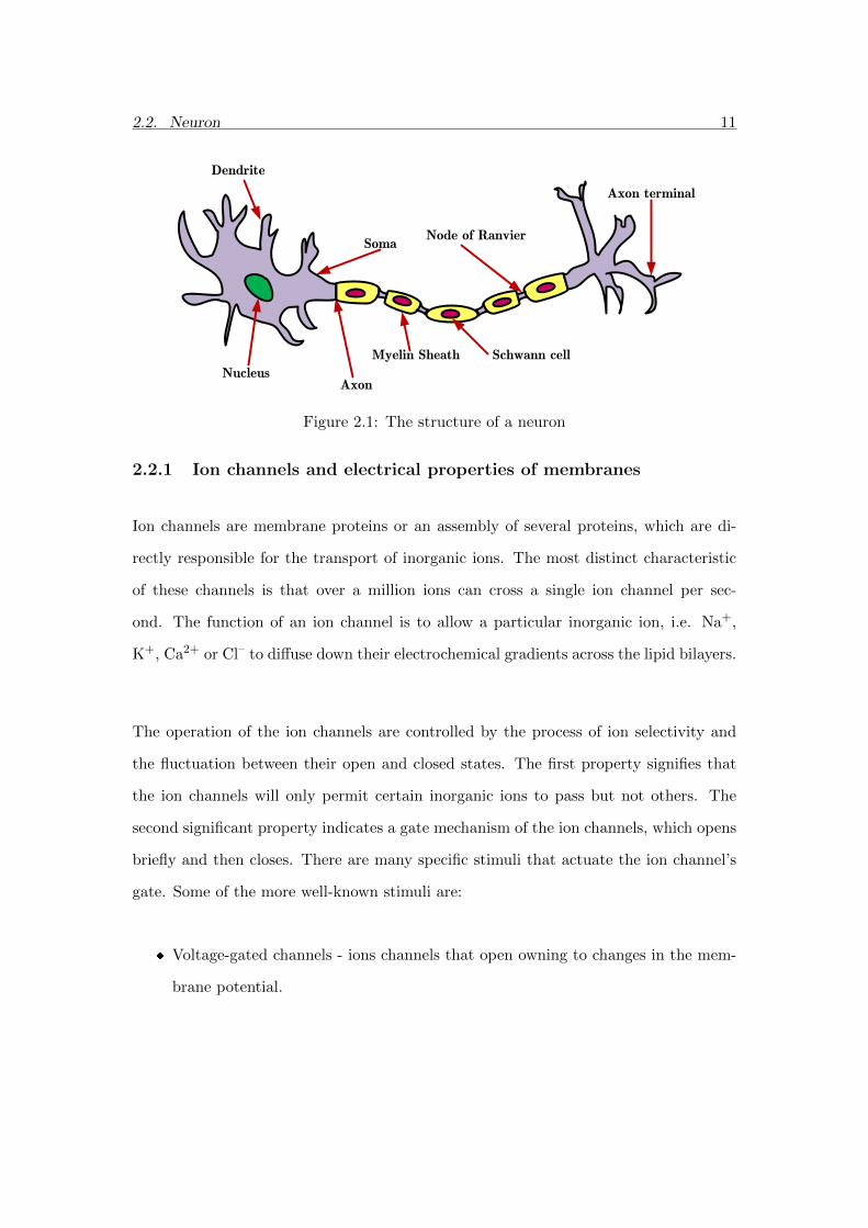
components of a typical neuron consist of the dendrites, a soma, a nucleus and the
axons as shown in Fig.(2.1).
Another unique property of neurons is the ability to transmit electrical signals over long
distances [9]. These signals travel through the cell membrane, which contains several
types of ion channels that interact with the changes in the transmembrane potential. A
transient pulse of charges across this transmembrane is called an action potential [10].
2.2. Neuron 11
Dendrite
Nucleus
Soma
Axon
Myelin Sheath Schwann cell
Node of Ranvier
Axon terminal
Figure 2.1: The structure of a neuron
2.2.1 Ion channels and electrical properties of membranes
Ion channels are membrane proteins or an assembly of several proteins, which are di-
rectly responsible for the transport of inorganic ions. The most distinct characteristic
of these channels is that over a million ions can cross a single ion channel per sec-
ond. The function of an ion channel is to allow a particular inorganic ion, i.e. Na+,
K+, Ca2+ or Cl– to diffuse down their electrochemical gradients across the lipid bilayers.
The operation of the ion channels are controlled by the process of ion selectivity and
the fluctuation between their open and closed states. The first property signifies that
the ion channels will only permit certain inorganic ions to pass but not others. The
second significant property indicates a gate mechanism of the ion channels, which opens
briefly and then closes. There are many specific stimuli that actuate the ion channel’s
gate. Some of the more well-known stimuli are:
� Voltage-gated channels - ions channels that open owning to changes in the mem-
brane potential.

2.2. Neuron 12
� Mechanical gated channels - ion channels that open under a mechanical stress.
� Ligand-gated channels - ion channels that are stimulated by the binding of a
ligand. This ligand can be either an extracellular mediator (a neurotransmitter
or transmitted-gated channel), an intracellular mediator (ion-gated channel) or a
nucleotide (nucleotide-gated channels).
Most ion channels are sensitive to K+ ions. When these ion channels operate, their
common function is to make the plasma membrane more permeable to K+ ions. This
behaviour plays a vital role in the regulation of the membrane potential.
The potential difference between the inside and the outside of the membrane, termed
the membrane potential, arises from the difference in electrical charges between the two
sides of the membrane. In humans, the Na+ - K+ pump assists in the maintenance of
the osmotic balance across the cell membrane by keeping a lower concentration of Na+
ions on the inside compared to the outside the cell.
2.2.2 Nernst Equation
The flow of any ions through a membrane channel is driven by the electrochemical gra-
dient. This gradient is influenced by both the voltage and the concentration gradient
of ions across the cell membrane.
When the influence of these two factors are balanced, the electrochemical gradient for
the ion is zero. The net flow of the ion channel is also zero. The membrane potential
(voltage gradient) at this equilibrium is given by the Nernst equation in eq.(2.1).
2.3. Action potential and its model 13
Vmem =RT
zFlnCoCi
(2.1)
where Vmem is the equilibrium membrane potential, CoCi
is the ratio of the outside to
the inside ion concentration, R is the gas constant (8314.4mJ/K·mol), T is the absolute
temperature in Kelvin, F is the Faraday’s constant 96, 485C/mol and z is the charge of
the ion.
For an animal cell, the potential difference across the plasma membrane at equilibrium
varies from -20mV to -200mV depending on the organism and the cell type. In hu-
man beings, this potential at equilibrium, termed the resting potential is given by the
Goldman equation shown in eq.(2.2)
Vmem = 58mV lnPK [K+]out + PNa[Na
+]out + PCl[Cl−]out
PK [K+]in + PNa[Na+]in + PCl[Cl−]in(2.2)
where PK , PNa and PCl are the relative membrane permeability for K+, Na+ and
Cl− ions. [K+], [Na+] and [Cl−] are the concentration of the potassium, sodium and
chloride ion. The subscriptions out and in refer to the outside and the inside of the
membrane, respectively.
2.3 Action potential and its model
2.3.1 Generation of Action Potential
An action potential is triggered when the plasma membrane potential rises above its
resting value. This event is termed as depolarisation. Depolarisation is the consequence

2.3. Action potential and its model 14
of a neurotransmitter-triggered response by the cell body. Owing to this depolarisation,
the voltage-gated channel for the sodium ions opens and allows Na+ ions to move inside
the cell. The amount of this migration is in accordance with its electrochemical gradient.
This open state of the Na+ channel remains until the membrane potential rises to
+50mV from the -70mV resting potential.
At a membrane potential of +50mV, a new equilibrium state is reached. However, the
duration of this peak is short owing to an automatic inactivation of the Na+ channels.
This mechanism forces the sodium channels to shut rapidly even when the membrane
is depolarised. With the sodium channels closed, the activation of the K+ channels
begins to bring the membrane potential back to the resting level (-70mV). The opening
of the K+ channels causes the K+ ions to dominate over the Na+ ions, which drives
the membrane potential back towards the K+ ion equilibrium point. Fig.(2.2) shows a
typical profile of an action potential as described above.
2.3.2 Membrane potential model
The membrane potential has been modelled mathematically in various forms. The very
first model, the integrate and fire model, was published in 1907 by Lapicque [11]. No
correlation between the membrane potential and the biophysical details was given in
this model. The first qualitative membrane potential with correlation to the biophys-
ical details was constructed from the experiment on a squid giant axon by Hodgkin
and Huxley in 1952 [12]. The Hodgkin and Huxley model is based on three main ionic
currents - sodium, potassium and leakage. More details on the Hodgkin and Huxley
model will be described in a later section.

2.3. Action potential and its model 15
Synaptic vesicle
Voltage-gated
Ca++ channels
Neurotransmitter
receptors
Postsynaptic
neuron
Presynaptic
neuron
Axon
terminal
Synaptic
cleft
Dendrite
spine
Vpre
Vpost
Threshold of
excitation
Na+ channels
open, Na+
begins to enter
cell
K+ channels
open, K+
begins to leave
cell
Na+ channels
become
refractory, no
more Na+
enters cell
K+ continues to
leave cell and
causes membrane
potential to return
to the resting potential
K+ channels close,
Na+ channels rest
Extra K+ outside
Diffuses away
-70
+40
1
2
3
4
5
6
Me
mb
ran
e p
ote
nti
al
(mV
)
time
Figure 2.2: Typical Nerve Action Potential
The mechanism of the potassium and the sodium channels in the Hodgkin and Huxley
model are described by non-linear, time-dependent functions. Thus, the computational
algorithm or the electronic circuit implementation of the Hodgkin and Huxley model will
be complex. More recently, there has been several attempts to re-model the membrane
potential with a less complex mathematical function while still exhibiting the neuron
behaviour in the Hodgkin and Huxley model. In this section, three other membrane po-
tential models will be described: Integrate-and-Fire, FitzHughNagumo and MorrisLecar
model.

2.3. Action potential and its model 16
� Integrate-and-Fire model: the simplest and the first model, proposed in 1907 by
Lapicque [11]. This model is based on the current and voltage of a capacitor,
given by:
I(t) = CmdV
dt(2.3)
where I(t) is the applied current, Cm is the membrane capacitance and V is the
membrane potential. When the current is applied, the membrane potential rises
until the threshold voltage (Vth) is reached. After reaching Vth, the membrane
potential will reset itself to the resting potential. From the hardware implemen-
tation aspect, the integrate and fire model is the most compact among the neuron
models.
� FitzHugh-Nagumo model: the model was published in 1961 by FitzHugh [13] and
later realised using electrical circuits by Nagumo et al. [14].
dV
dt= V − V 3
3−W + I
dW
dt= 0.08(V + 0.7− 0.8W )
(2.4)
where W is the recovery variable and I is the stimulus current.
The FitzHugh-Nagumo model can be classified as a reduced version of the Hodgkin
and Huxley model because the three current compartments (Na+, K+ and leakage)
have been reduced into a single variable equation.
� Morris-Lecar model: another simplified model of Hodgkin and Huxley. There are
three current channels in this model: Ca2+, K+ and leakage. The equations for

2.3. Action potential and its model 17
this model are [15]:
CmdV
dt= −gCaMss(V )(V − ECa)− gKW (V − EK)− gL(V − EL) + I
dW
dt=Wss(V )−W
τW (V )
Mss =1 + tanh[V−V1V2
]
2
Wss =1 + tanh[V−V3V4
]
2
τW (V ) = τ0sech(V − V3
2V4)
(2.5)
where W is the recovery parameter. gCa and gK are the conductance of calcium
and potassium channels, respectively. ECa and EK are the equilibrium potential
for calcium and potassium. Mss and Wss are the open state probability.
The Morris-Lecar model preserves the chemical channels as in the Hodgkin and
Huxley model. More importantly, the open state equation for each channel is less
complex and is more straightforward to implement than the Hodgkin and Huxley
model.
2.3.3 Hodgkin and Huxley model
The first qualitative mathematical model of an action potential was published by Alan
L. Hodgkin and Andrew Huxley in 1952 [12, 16, 17, 18, 19]. From the voltage clamp
experiment along the axon of a giant squid, Hodgkin and Huxley observed that the
electrical current across the cell membrane depended on two factors:
1. The resistance of the cell membrane, and
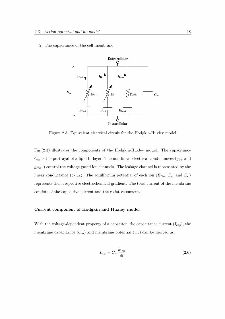
2.3. Action potential and its model 18
2. The capacitance of the cell membrane
gNa+ gK+ gLeak
ENa+ EK+ ELeak
INa+ IK+ ILeak
VmCm
Extracellular
Intracellular
Figure 2.3: Equivalent electrical circuit for the Hodgkin-Huxley model
Fig.(2.3) illustrates the components of the Hodgkin-Huxley model. The capacitance
Cm is the portrayal of a lipid bi-layer. The non-linear electrical conductances (gk+ and
gNa+) control the voltage-gated ion channels. The leakage channel is represented by the
linear conductance (gLeak). The equilibrium potential of each ion (ENa, EK and EL)
represents their respective electrochemical gradient. The total current of the membrane
consists of the capacitive current and the resistive current.
Current component of Hodgkin and Huxley model
With the voltage-dependent property of a capacitor, the capacitance current (Icap), the
membrane capacitance (Cm) and membrane potential (vm) can be derived as:
Icap = Cmdvmdt
(2.6)
2.3. Action potential and its model 19
The resistive current is the voltage-dependent current (both membrane and equilibrium
potential). The equilibrium potential of individual channels can be calculated from
the Nernst equation (eq.(2.1)). From the circuit point of view, the ionic current in
the membrane is directly proportional to the difference between the membrane and
equilibrium potential, as shown in eq.(2.7).
Iion = gion(vm − Eion) (2.7)
The total membrane current (Im) for the model proposed by Hodgkin and Huxley can
be given as:
Im = Icap + Iion (2.8)
Im = Cmdvmdt
+ gion(vm − Eion) (2.9)
Im = Cmdvmdt
+
INa︷ ︸︸ ︷gNa(t)(vm − ENa) +
IK︷ ︸︸ ︷gK(t)(vm − EK) +
IL︷ ︸︸ ︷gL(vm − EL) (2.10)
where gNa(t), gK(t) and gL are the conductance of the sodium, potassium and leakage
channel, respectively. ENa, EK and EL are the equilibrium potential of the sodium,
potassium and leakage channel.
The experiment of Hodgkin and Huxley also concluded that gNa(t) and gK(t) are non-
linear conductances whilst gL is linear. The time-dependence of the potassium and
sodium channels was modelled by introducing a new variable that refers to the proba-

2.3. Action potential and its model 20
bility of the ionic gating process. This will be shown in the next section.
Note that the lowercase, vm, is the difference in the membrane potential, Vm(t), and its
resting value, Vm(rest). Thus, the definition of vm is:
vm(t) = Vm(t)− Vm(rest) (2.11)
From eq.(2.11), vm mathematically differs from Vm(t) by a constant. This means that
the time-derivation of vm is equal to the corresponding derivatives of Vm(t).
Mathematical model for the potassium channel
The potassium conductance gK(t, vm) is the fixed maximum conductance (when all
channels are open), gK , multiplied by n4: the fraction of the open channels (0 < n < 1).
Thus,
gK(t, vm) = gKn4(t, vm) (2.12)
The variable n can be derived from the first order kinetics:
dn(t, vm)
dt= αn(vm)(1− n)− βn(vm)n (2.13)
From curve fitting, the rate constants αn(vm) and βn(vm) are:
αn =0.01(10 + vm)
exp(10+vm10 )− 1
(2.14)
2.3. Action potential and its model 21
and
βn = 0.125 exp(vm80
) (2.15)
where vm is in mV and α, β are in (milli-second)−1. The potassium channel current is
given by:
IK = gKn4(vm − EK) (2.16)
Mathematical model for the sodium channel
The ionic current for the sodium channel has a similar model to the potassium channel,
except that there are two control probability variables: m (activation) and h (inactiva-
tion), where:
gNa(t, vm) = gNam3(t, vm)h(t, vm) (2.17)
Both parameters follow the first-order differential equation similar to the variable n in
the potassium channel as:
dm(t, vm)
dt= αm(vm)(1−m)− βm(vm)m (2.18)
and
dh(t, vm)
dt= αh(vm)(1− h)− βh(vm)h (2.19)

2.3. Action potential and its model 22
The rate constants - αm, βm, αh and βh - were chosen from the curve fitting as:
αm =0.1(25 + vm)
exp(25+vm10 )− 1
(2.20)
βm = 4 exp(vm18
) (2.21)
and
αh = 0.07 exp(vm20
) (2.22)
βh =1
exp(30+vm10 ) + 1
(2.23)
where vm is in mV and α, β are in (milli-second)−1. The sodium channel current is
given by:
INa = gNam3h(vm − ENa) (2.24)
Mathematical model for the leakage channel
As stated earlier, the conductance of the leakage channel is considered as a constant.
Thus, the leakage channel current is given by:
IL = gL(vm − EL) (2.25)

2.3. Action potential and its model 23
The value of the variables mentioned in the sodium, potassium and leakage channel is
shown in Table (2.1).
Table 2.1: Hodgkin and Huxley nerve axon model parametersConstant Name Units Values
Cm Membrane capacitance µF/cm2 1 to 2.8
ENa Sodium equilibrium potential mV Vm(rest) + 115
EK Potassium equilibrium potential mV Vm(rest)− 12
EL Leakage equilibrium potential mV Vm(rest)− 10.613
gNa Sodium maximum conductance mS/cm2 120
gK Potassium maximum conductance mS/cm2 36
gL Leakage maximum conductance mS/cm2 0.3
2.3.4 Single Compartment
In Table(2.1), some units of the Hodgkin and Huxley model parameter are per unit area.
Therefore, to synchronise the Hodgkin and Huxley model with the chemical synapse, a
single neuron model, those units has to be transformed for a single compartment neuron.
Firstly, the exact area of a single neuron needs to be calculated. A single compartment of
neurons is 10µm in diameter, 10µm in length (i.e. area of single neuron is π×10−6cm2)
[20]. The transformed parameters from Table(2.1) are shown in Table(2.2).
Table 2.2: Transformed Hodgkin and Huxley axon model parametersConstant Name Units Values
Cm Membrane capacitance pF 3.14159 to 8.79645
gNa Sodium maximum conductance nS 376.9911184
gK Potassium maximum conductance nS 113.0973355
gL Leakage maximum conductance nS 0.9424777961
Furthermore, the unit of vm in eq.(2.14), eq.(2.15), eq.(2.20), eq.(2.21), eq.(2.22) and
eq.(2.23) is mV. To standardise this unit, these equations need to be transformed into
Volts. The transformations are shown in eq.(2.26) to eq.(2.31).

2.3. Action potential and its model 24
αn =104(0.01 + vm)
exp(0.01+vm0.01 )− 1
(2.26)
βn = 125 exp(vm
0.08) (2.27)
The graph plots in MATLAB of eq.(2.26) and (2.27) are shown in Fig.(2.4).
(a) (b)
Figure 2.4: Rate constants (a) αn and (b) βn
The activation of the open state for the potassium channel (n) is a function of αn and
βn i.e. the first order differential equation as shown in eq.(2.13). The plot of the n
variable is shown in Fig.(2.5).
αm =105(0.025 + vm)
exp(0.025+vm0.01 )− 1
(2.28)
βm = 4×10³ exp(vm
0.018) (2.29)

2.3. Action potential and its model 25
Figure 2.5: Activation of potassium channel (n)
The graph plots in MATLAB of eq.(2.28) and (2.29) are shown in Fig.(2.6).
(a) (b)
Figure 2.6: Rate constants (a) αm and (b) βm
The activation variable of the sodium channel (m) is a function of αm and βm i.e. the
first order differential equation as shown in eq.(2.18). The plot of the variable m is
shown in Fig.(2.7).

2.3. Action potential and its model 26
Figure 2.7: Activation of the sodium channel (m)
αh = 70 exp(vm
0.02) (2.30)
βh =103
exp(0.03+vm0.01 ) + 1
(2.31)
The graph plots in MATLAB of eq.(2.30) and (2.31) are shown in Fig.(2.8).
(a) (b)
Figure 2.8: Rate constant (a) αh and (b) βh

2.3. Action potential and its model 27
The inactivation variable for the sodium channel (h) is a function of αh and βh i.e.
the first order differential equation as shown in eq.(2.19). The plot of the variable h is
shown in Fig.(2.9).
Figure 2.9: Inactivation of the sodium channel (h)
The action potential according to eq.(2.10) was also plotted. Its result is illustrated in
Fig.(2.10).
(a) (b)
Figure 2.10: (a) The action potential (vm) observed when applied with (b) the totalmembrane current (Im)

2.4. The Synapse 28
2.4 The Synapse
Communication between neurons is achieved via the transmission of action potentials.
This transmission is facilitated by synapses which acts as the medium. Synapses have
a bulb-like structure and their function is to interconnect neurons with other targeted
neurons. The synapse is the crucial part of a the neural communication system because
it allows a neuron to instantly relay signals to one or more other neurons [21]. Synapses
can be categorised into two types: electrical and chemical.
2.4.1 Electrical Synapse
For the electrical synapse shown in Fig.(2.11), the depolarisation of the presynaptic
neuron is directly coupled to the postsynaptic neuron without any delay. The pre- and
postsynaptic membrane of the electrical synapse are separated by a small gap junction
(3.5nm). The transmission of action potentials for this instance is simply a directly
connected ionic current.
Owing to the ionic current movement at the gap junction, the direction of the trans-
mission at the electrical synapses can be bidirectional. Other remarkable properties of
electrical synapses are their speed and reliability. The delay due to this type of synaptic
transmission is very small and can be negligible.
2.4.2 Chemical Synapse
In contrast with electrical synapses where the pre- and postsynaptic neurons are ad-
hered to each other, the pre- and postsynaptic membrane of chemical synapses shown
in Fig.(2.12) have a larger separation (20-40 nm), called a synaptic cleft. As a result,

2.4. The Synapse 29
Gap junction
Figure 2.11: Electrical synapse
chemical synapses rely on the release of neurotransmitters from the presynaptic neuron.
The neurotransmitters are stored in the synaptic vesicles at the presynaptic terminal.
Once these neurotransmitters are emitted into the synaptic cleft, they will bind to a
specific receptor at the postsynaptic neuron.
The detail of the chemical synaptic events from the pre- to the postsynaptic cell is
summarised as [21]:
1. In the bouton of the postsynaptic neuron, the neurotransmitters are filled within
the vesicles. Most of these vesicles are incapacitated. When the presynaptic action
potential reaches the terminal arborisation of a bouton, the depolarisation induces
the voltage-gated calcium channel proteins to open and accept Ca2+ ions, which
causes the concentration of Ca2+ to increase from 100 nM to 100 µM.

2.4. The Synapse 30
Synaptic vesicle
Voltage-gatedCa++ channels
Neurotransmitterreceptors
Presynapticneuron
Postsynapticneuron
Axonterminal
Synapticcleft
Dendritespine
Figure 2.12: Chemical synapse
2. An increase of intracellular [Ca2+] causes the vesicles to deliquesce and release
their neurotransmitters into the synaptic cleft. This process is called exocytosis.
3. The released neurotransmitter molecules bind to the receptors on the postsynaptic
cell membrane. This binding process leads to the opening and closing of ion
channels. The resulting ionic flux causes the membrane conductance and the
membrane potential of the postsynaptic cell to fluctuate.
Table (2.3), below, summarises the contrasting properties of electrical and chemical
synapses.
2.4.3 Biological model for the chemical synapse
Model of neurotransmitter release
The relationship between the presynaptic action potential and the release of the neu-
rotransmitter has been described in a mathematical model [22], which was simplified

2.4. The Synapse 31
Table 2.3: Summary Properties of SynapsesProperty Electrical Synapse Chemical Synapse
Distance between pre- 3.5 nm 16-20 nmand postsynaptic cell membranes
Cytoplasmic continuity between Yes Nopre- and postsynaptic cells
Ultrastructural components Gap-junction channels Presynaptic vesicles
Agent of transmission Ion current Chemical transmitter
Synaptic delay Negligible 0.3-5 ms, depending
Direction of transmission Generally bidirectional Generally unidirectional
from the calcium-induced release model [23]. Eq.(2.32) shows the relationship between
the neurotransmitter concentration [T ] and the presynaptic voltage Vpre as:
[T ](Vpre) =Tmax
1 + exp [−(Vpre − Vp)/Kp](2.32)
where Tmax is the maximal concentration of the neurotransmitter in the synaptic cleft,
Kp is the steepness and Vp is the half-activated function.
Kinetic model of the synapse
The relationship between the postsynaptic response and the neurotransmitter concen-
tration was proposed by Destexhe et al. [20]. This response can be described in the
first order kinetic regime as:
R+ Tα
GGGGGBFGGGGG
βTR∗ (2.33)
where R and TR∗ are the unbound and bound state of the postsynaptic receptors, re-
spectively. α and β are the forward and backward rate constant for the neurotransmitter
binding. The fraction of bound receptor for this model is expressed using the law of

2.4. The Synapse 32
mass action [24], stated as:
dr
dt= α[T ](1− r)− βr (2.34)
where [T ] is the concentration of the neurotransmitter and r is defined as the fraction of
the receptors in the open state. This neurotransmitter concentration is simplified and
modelled as a pulse with a 1 ms duration and a 1 mM amplitude.
Model for the postsynaptic transmission
The mathematical model of the postsynaptic transmission has been simplified from the
Markov model of the postsynaptic current [25]. The postsynaptic membrane voltage
(Vpost) consists of the voltage-gated ion channels current (Iion) and the synaptic current
(Isyn), as shown in eq.(2.35) and eq.(2.36).
CmdVpostdt
= −(Iion + Isyn) (2.35)
Isyn = gsyn(t)(Vpost − Esyn) (2.36)
where Cm is the membrane capacitance, gsyn(t) is the time-dependent synaptic conduc-
tance and Esyn is the reversal potential of the channel.
There are four types of receptors that have been modelled [25]: AMPA, NMDA,
GABAA and GABAB. AMPA and NMDA are classified as the EPSP (excitatory
postsynaptic potential) whilst GABAA and GABAB are considered as the IPSP (in-
2.4. The Synapse 33
hibitory postsynaptic potential). The postsynaptic current for each receptor is described
as:
AMPA receptor:
drAMPA
dt= αAMPA [T ](1− rAMPA)− βAMPArAMPA (2.37)
IAMPA = gAMPA
rAMPA(V − EAMPA) (2.38)
where gAMPA
is the maximal conductance (approximately 0.35− 1.0 nS), rAMPA is the
fraction of the receptor in the open state, V is the postsynaptic potential and EAMPA
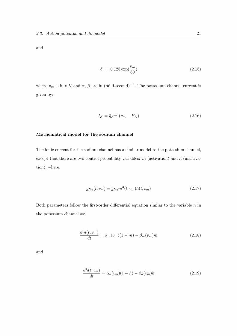
is the reversal potential (= 0mV). Obtaining the best fit from the kinetic scheme,
αAMPA = 1.1 × 10⁶ and βAMPA = 190. The plot of the variable rAMPA is shown in
Fig.(2.13).
Figure 2.13: MATLAB simulation of rAMPA

2.4. The Synapse 34
NMDA receptor:
drNMDA
dt= αNMDA [T ](1− rNMDA)− βNMDArNMDA (2.39)
B(V ) =1
1 + exp (−0.062V )[Mg2+]o3.57
(2.40)
INMDA = gNMDA
B(V )rNMDA(V − ENMDA) (2.41)
where gNMDA
is the maximal conductance (approximately 0.01 − 0.6 nS), B(V ) is the
magnesium block, [Mg2+]o is the external magnesium concentration (1 to 2 mM in
physiological conditions), rNMDA is the fraction of the receptors in the open state, V
is the postsynaptic potential and ENMDA is the reversal potential (= 0mV). Obtaining
the best fit from the kinetic scheme, αNMDA = 7.2× 10⁴ and βNMDA = 6.6. The plot of
the variable rNMDA is shown in Fig.(2.14).
Figure 2.14: MATLAB simulation of rNMDA
2.4. The Synapse 35
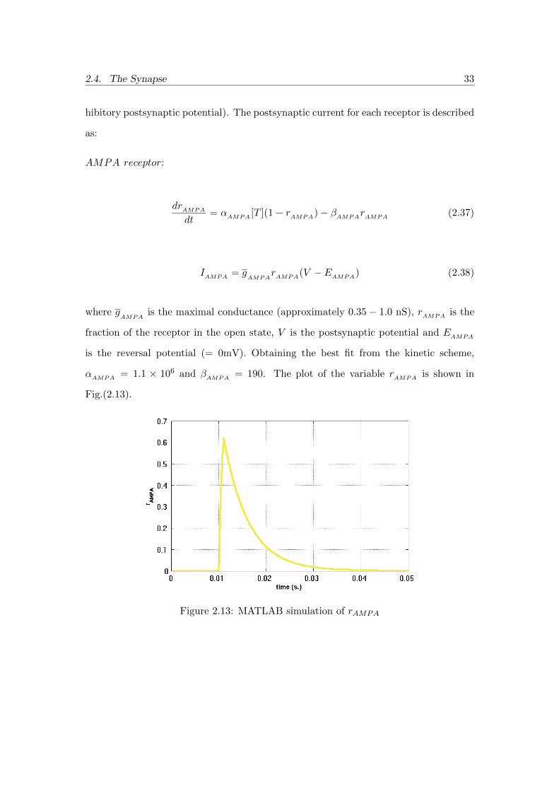
GABAA receptor:
drGABAAdt
= αGABAA [T ](1− rGABAA )− βGABAA rGABAA (2.42)
IGABAA = gGABAA
rGABAA (V − EGABAA) (2.43)
where gGABAA
is the maximal conductance (approximately 0.25-1.2 nS), rGABAA is the
fraction of the receptors in the open state, V is the postsynaptic potential and EGABAA
is the reversal potential (= -70 mV). Obtaining the best fit from the kinetic scheme,
αGABAA = 5.3 × 10⁵ and βGABAA=180. The plot of the variable rGABAA is shown in
Fig.(2.15).
Figure 2.15: MATLAB simulation of rGABAA
GABAB receptor:
drGABABdt
= K1 [T ](1− rGABAB )−K2rGABAB (2.44)

2.4. The Synapse 36
du
dt= K3rGABAB −K4u (2.45)
IGABAB = gGABAB
u4
u4 +Kd(V − EGABAB
) (2.46)
where gGABAB
is the maximal conductance (approximately 1 nS), rGABAB is the fraction
of the activated receptors, V is the postsynaptic potential, u is the concentration of
activated G-protein, and EGABABis the reversal potential (= -95 mV). From curve
fitting, the following values were obtained: Kd = 100µM4, K1 = 9×10⁴ M−1s−1,
K2 = 1.2 s−1, K3 = 180 s−1, K4 = 34 s−1 and n = 4 binding site. The plot of the
variable rGABAA is shown in Fig.(2.16).
Figure 2.16: MATLAB simulation of rGABAB
2.4.4 Postsynaptic simulation
The postsynaptic potential of the AMPA, NMDA, GABAA and GABAB receptors
are simulated according to eq.(2.35). The terms Iion and Isyn in this equation refer to
the Hodgkin and Huxley ionic current and the synaptic receptor current, respectively.
The resting potential in this case is assumed to be 100mV. The Hodgkin and Huxley

2.4. The Synapse 37
parameters for this resting potential are:
αn =104(0.11 + Vm)
exp(0.11+Vm0.01 )− 1
βn = 125 exp(0.1 + Vm
0.08)
dn
dt= αn(1− n)− βnn
αm =105(0.125 + Vm)
exp(0.125+Vm0.01 )− 1
βm = 4×10³ exp(0.1 + Vm
0.018)
dm
dt= αm(1−m)− βmm
αh = 70 exp(0.1 + Vm
0.02) βh =
103
exp(0.13+Vm0.01 ) + 1
dh
dt= αh(1− h)− βhh
The potassium, sodium and leakage currents for a 100mV resting potential are:
IK = gKn4(Vm − 0.112) INa = gNam
3h(Vm + 0.015) IL = gL(Vm − 0.089387)
The simulation of the postsynaptic transmission for the AMPA, NMDA, GABAA and
GABAB receptors are shown below.
AMPA postsynaptic simulation
The postsynaptic simulation of the AMPA receptor was based on:
CmdVmdt
= −INa − IK − IL − IAMPA
IAMPA = gAMPArAMPA(Vm − EAMPA)(2.47)
where the reversal potential for AMPA (EAMPA) with a 100mV resting potential is
170mV and the maximal conductance for AMPA (gAMPA) is 0.1nS. The MATLAB
2.4. The Synapse 38
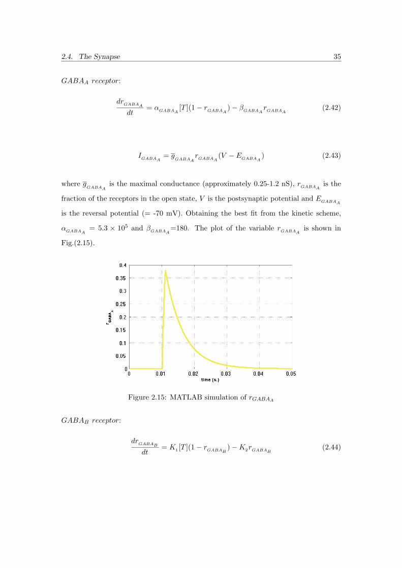
simulation of the AMPA receptor is shown in Fig.(2.17) and (2.18).
(a) (b)
Figure 2.17: (a) Single spike of AMPA neurotransmitter and (b) its postsynaptic re-sponse
(a) (b)
Figure 2.18: (a) Four spikes of AMPA neurotransmitter and (b) its postsynaptic re-sponse
NMDA postsynaptic simulation
The postsynaptic simulation of the NMDA receptor was based on:
CmdVmdt
= −INa − IK − IL − INMDA
INMDA = gNMDAB(Vm)rNMDA(Vm − ENMDA)
B(Vm) =1
1 + exp (−0.062Vm)[Mg2+]o3.57
(2.48)

2.4. The Synapse 39
where the reversal potential for NMDA (ENMDA) with a 100mV resting potential is
170mV and the maximal conductance for NMDA (gNMDA) is 0.1nS. The MATLAB
simulation of the NMDA receptor is shown in Fig.(2.19) and (2.20).
(a) (b)
Figure 2.19: (a) Single spike of NMDA neurotransmitter and (b) its postsynapticresponse
(a) (b)
Figure 2.20: (a) Four spikes of NMDA neurotransmitter and (b) its postsynaptic re-sponse
GABAA postsynaptic simulation
The postsynaptic simulation for the GABAA receptor was based on:

2.4. The Synapse 40
CmdVmdt
= −INa − IK − IL − IGABAA
IGABAA = gGABAArGABAA(Vm − EGABAA)(2.49)
where the reversal potential for GABAA (EGABAA) with a 100mV resting potential is
90mV and the maximal conductance for GABAA (gGABAA) is 0.1nS. The MATLAB
simulation of the GABAA receptor is shown in Fig.(2.21) and (2.22).
(a) (b)
Figure 2.21: (a) A single spike of GABAA neurotransmitter and (b) its postsynapticresponse
(a) (b)
Figure 2.22: (a) Four spikes of GABAA neurotransmitter and (b) its postsynapticresponse
2.4. The Synapse 41
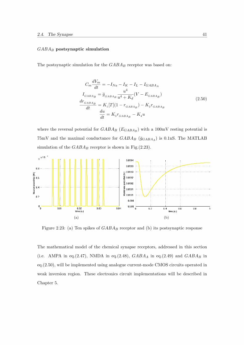
GABAB postsynaptic simulation
The postsynaptic simulation for the GABAB receptor was based on:
CmdVmdt
= −INa − IK − IL − IGABAA
IGABAB = gGABAB
u4
u4 +Kd(V − EGABAB
)
drGABABdt
= K1 [T ](1− rGABAB )−K2rGABABdu
dt= K3rGABAB −K4u
(2.50)
where the reversal potential for GABAB (EGABAB ) with a 100mV resting potential is
75mV and the maximal conductance for GABAB (gGABAA) is 0.1nS. The MATLAB
simulation of the GABAB receptor is shown in Fig.(2.23).
(a) (b)
Figure 2.23: (a) Ten spikes of GABAB receptor and (b) its postsynaptic response
The mathematical model of the chemical synapse receptors, addressed in this section
(i.e. AMPA in eq.(2.47), NMDA in eq.(2.48), GABAA in eq.(2.49) and GABAB in
eq.(2.50), will be implemented using analogue current-mode CMOS circuits operated in
weak inversion region. These electronics circuit implementations will be described in
Chapter 5.
2.5. Silicon neuromorphic circuits 42
2.5 Silicon neuromorphic circuits
Since the idea of implementing neuromorphic systems on silicon was initiated by Mead
and his collaborators in the late 1980s and the early 1990s [1, 26], bio-inspired systems
on the CMOS platform has captured many researchers’ imagination.
In this section, reviews of the silicon neurons (mostly based on the Hodgkin-Huxley
model) and the synapse models will be presented.
2.5.1 Silicon Neurons
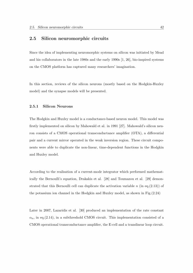
The Hodgkin and Huxley model is a conductance-based neuron model. This model was
firstly implemented on silicon by Mahowald et al. in 1991 [27]. Mahowald’s silicon neu-
ron consists of a CMOS operational transconductance amplifier (OTA), a differential
pair and a current mirror operated in the weak inversion region. These circuit compo-
nents were able to duplicate the non-linear, time-dependent functions in the Hodgkin
and Huxley model.
According to the realisation of a current-mode integrator which performed mathemat-
ically the Bernoulli’s equation, Drakakis et al. [28] and Toumazou et al. [29] demon-
strated that this Bernoulli cell can duplicate the activation variable n (in eq.(2.13)) of
the potassium ion channel in the Hodgkin and Huxley model, as shown in Fig.(2.24)
Later in 2007, Lazaridis et al. [30] produced an implementation of the rate constant
αn, in eq.(2.14), in a subthreshold CMOS circuit. This implementation consisted of a
CMOS operational transconductance amplifier, the E-cell and a translinear loop circuit.

2.5. Silicon neuromorphic circuits 43
Na+
chan
nel
g L
INa IL
EL
Cmem
nI
nn II
Iout
I0
I0IK(Iout1)
K+ channel
Figure 2.24: Hodgkin and Huxley implementation on CMOS of Toumazou et al. [29]
Lazaridis ’s work illustrated the ability to fully implement the Hodgkin and Huxley neu-
ron model on the CMOS platform.
Owing to the complexity of the mathematics required to calculate the variables in the
Hodgkin and Huxley model that is reflected by the circuit realisation, Farquhar et al.
proposed a contrasting idea to implement the Hodgkin and Huxley model with less
components than previous designs [31]. In Farquhar’s work, the similarity between
the non-linear characteristics of the MOSFET current and those of the variables in the
Hodgkin and Huxley model were compared. As a result, Farquhar succeeded in creating
a CMOS version of the Hodgkin and Huxley neuron with just six MOSFETs and three
capacitors.

2.5. Silicon neuromorphic circuits 44
2.5.2 Silicon Synapses
Ludovic et al. [32] created a Bi-CMOS circuit to duplicate the fraction of the receptors
in the open state (r), in eq.(2.34). This was achieved by transforming eq.(2.34) into an
exponential decay function, where a resistive-capacitive circuit was employed together
with a bipolar junction transistor (BJT) to formulate this function. This work can be
considered as the first CMOS synapse based on the model of Destexhe [22].
In 2006, Lazaridis et al. applied the Bernoulli cell [33] to duplicate r with a weakly
inverted CMOS circuit. The Bernoulli cell implementation of r required four NMOS
transistors and a capacitor. This circuit configuration, shown in Fig.(2.25) is equivalent
to a current-mode low pass filter. This synapse circuit based on the model of Destexhe
[22] is the first implementation which employs the CMOS current mode log domain
filter in subthreshold CMOS technology.
A synapse implemented with only a few transistors and capacitors was reported by Gor-
don et al. [34]. This idea uses a floating gate MOSFET where its gate was controlled
with biased capacitors and a CMOS inverter. Gordon’s synapse transistor circuit is
shown in Fig.(2.26).
This floating gate MOSFET with a CMOS inverter gave a waveform which fits the bi-
ological synapse model of Rall [35]. Furthermore when the bias potential of this circuit
was properly tuned, its output waveform would match the postsynaptic potential of
the excitatory and inhibitory synapse recorded from the neurons experiment of Wall
et al. [36]. However, this floating gate CMOS circuit is not suitable for implantable
applications. This is because the high current and high voltage properties of this circuit

2.5. Silicon neuromorphic circuits 45
inVinV
outI
1xI
2xI
bI
outI
M1 M2
1DI2DI
X
2
inV
2
inV
SV
GVBV
DSi
DV
T
gsDS
nU
VVI )(
T
bsDS
nU
VVIn )()1(
dV
gVbVDSi
+n
n 1
n
1
+-
-
1
bV
gV
sV
DSi
bI
outI
2
inV
2
inV
Na
+ c
ha
nn
el
gL
INa IL
EL
Cmem
nI
nn II
Iout
I0
I0IK(Iout1)
K+ channel
I][TI
I0][TI
I0
Iout
Figure 2.25: r implementation with a Bernoulli cell by Lazaridis et al. [33]
might be harmful to organisms.
Another interesting work on a biomimetic synapse is the use of a MOSFET-based mem-
ory device to match the function of a synapse. Yu et al. [37] reported the potential use
of a metal oxide resistive switching memory for this application. This device is made of
Titanium Nitride (TiN), Hafnium Oxide (HfOx), Aluminium Oxide (AlOx) and Plat-
inum (Pt), as the base materials. This non-volatile memory device is a simple capacitor
network which performs an integration to duplicate the function of synapses. The ben-
efit from the synapse implementation on this approach is that it requires comparatively
smaller chip area than the conventional electronic circuit.
From the implementations of the synapse shown earlier in this section, there are no

2.6. Summary 46
inVinV
outI
1xI
2xI
bI
outI
M1 M2
1DI2DI
X
2
inV
2
inV
SV
GVBV
DSi
DV
T
gsDS
nU
VVI )(
T
bsDS
nU
VVIn )()1(
dV
gVbVDSi
+n
n 1
n
1
+-
-
1
bV
gV
sV
DSi
bI
outI
2
inV
2
inV
Na
+ c
ha
nn
el
gL
INa IL
EL
Cmem
nI
nn II
Iout
I0
I0IK(Iout1)
K+ channel
I][TI
I0][TI
I0
Iout
ECa
Vp
Vn
Vtun
Vin
Vout
Figure 2.26: Gordon’s synapse circuit
implementation that has been formulated for a specific receptor type or with actual
neurotransmitter sensing. The integration between an electronic circuit which performs
the chemical synapse function, and a chemical sensor, which has the capability to de-
tect neurotransmitters, will lead to a complete OR a fully-functional bionics chemical
synapse. An integrated implementation of the chemical synapse will be presented later
in Chapter 5.
2.6 Summary
In this chapter, the principle and the biological aspects of neurons were introduced. The
action potential, the signal used for neuron communication, was described. Further-
more, various models of the membrane potential were mathematically explained, such

2.6. Summary 47
as the Hodgkin-Huxley model, the integrate-fire model, the FitzHugh-Nagumo model
and the Morris-Lecar model. The Hodgkin-Huxley model was examined in greater de-
tail, especially the function of the current channels (Na and K) which was also simulated
in MATLAB.
The other main content of this chapter is the function of synapses. The chemical
synapse model by Destexhe was introduced and its simulation results on MATLAB
were shown. Moreover, from the aspect of the bio-inspired circuits, examples of the
silicon implementation of neurons and synapses were reviewed.
References
[1] R. F. Lyon and C. Mead, “An analog electronic cochlea,” Acoustics, Speech and
Signal Processing, IEEE Transactions on, vol. 36, no. 7, pp. 1119–1134, 1988.
[2] V. Chan, S.-C. Liu, and A. van Schaik, “Aer ear: A matched silicon cochlea pair
with address event representation interface,” Circuits and Systems I: Regular Pa-
pers, IEEE Transactions on, vol. 54, no. 1, pp. 48–59, 2007.
[3] B. Wen and K. Boahen, “A silicon cochlea with active coupling,” Biomedical Cir-
cuits and Systems, IEEE Transactions on, vol. 3, no. 6, pp. 444–455, 2009.
[4] J. Costas-Santos, T. Serrano-Gotarredona, R. Serrano-Gotarredona, and
B. Linares-Barranco, “A spatial contrast retina with on-chip calibration for neuro-
morphic spike-based aer vision systems,” Circuits and Systems I: Regular Papers,
IEEE Transactions on, vol. 54, no. 7, pp. 1444–1458, 2007.
[5] R. Serrano-Gotarredona, T. Serrano-Gotarredona, A. Acosta-Jimenez, and
B. Linares-Barranco, “A neuromorphic cortical-layer microchip for spike-based
event processing vision systems,” Circuits and Systems I: Regular Papers, IEEE
Transactions on, vol. 53, no. 12, pp. 2548–2566, 2006.
48
REFERENCES 49
[6] K. A. Zaghloul and K. Boahen, “Optic nerve signals in a neuromorphic chip II:
testing and results,” Biomedical Engineering, IEEE Transactions on, vol. 51, no. 4,
pp. 667–675, 2004.
[7] T. J. Koickal, A. Hamilton, S. L. Tan, J. A. Covington, J. W. Gardner, and T. C.
Pearce, “Analog vlsi circuit implementation of an adaptive neuromorphic olfaction
chip,” Circuits and Systems I: Regular Papers, IEEE Transactions on, vol. 54,
no. 1, pp. 60–73, 2007.
[8] D. Ottoson, Physiology of the Nervous System. Oxford University Press, 1983.
[9] E. Izhikevich, Dynamical Systems in Neuroscience: The Geometry of Excitability
and Bursting (Computational Neuroscience). The MIT Press, 11/01 2006.
[10] R. Plonsey and R. C. Barr, Bioelectricity : A Quantitative Approach. Springer,
2007.
[11] L. Lapicque, “Recherches quantitatives sur l’excitation electrique des nerfs traitee
comme une polarization,” J Physiol Pathol Gen, vol. 9, pp. 620–635, 1907.
[12] A. L. Hodgkin, A. F. Huxley, and B. Katz, “Measurement of current-voltage rela-
tions in the membrane of the giant axon of loligo,” J Physiol, vol. 116, no. 4, pp.
424–448, April 28 1952.
[13] R. FitzHugh, “Impulses and physiological states in theoretical models of nerve
membrane,” Biophysical journal, vol. 1, no. 6, pp. 445–466, 7 1961.
[14] J. Nagumo, S. Arimoto, and S. Yoshizawa, “An active pulse transmission line
simulating nerve axon,” Proceedings of the IRE, vol. 50, no. 10, pp. 2061–2070,
1962.
[15] C. Morris and H. Lecar, “Voltage oscillations in the barnacle giant muscle fiber,”
Biophysical journal, vol. 35, no. 1, pp. 193–213, 7 1981.
REFERENCES 50
[16] A. L. Hodgkin and A. F. Huxley, “A quantitative description of membrane current
and its application to conduction and excitation in nerve,” J Physiol, vol. 117,
no. 4, pp. 500–544, August 28 1952.
[17] A. L. Hodgkin and A. L. Huxley, “Currents carried by sodium and potassium ions
through the membrane of the giant axon of loligo,” J Physiol, vol. 116, no. 4, pp.
449–472, April 28 1952.
[18] A. Hodgkin and A. Huxley, “The components of membrane conductance in the
giant axon of loligo,” J Physiol, vol. 116, no. 4, pp. 473–496, April 28 1952.
[19] A. L. Hodgkin and A. L. Huxley, “The dual effect of membrane potential on sodium
conductance in the giant axon of loligo,” J Physiol, vol. 116, no. 4, pp. 497–506,
April 28 1952.
[20] A. Destexhe, Z. F. Mainen, and T. J. Sejnowski, “An efficient method for comput-
ing synaptic conductances based on a kinetic model of receptor binding,” Neural
computation, vol. 6, no. 1, pp. 14–18, 1994.
[21] R. B. Northrop, Introduction to Dynamic Modeling of Neuro-Sensory Systems.
CRC Press, 2000.
[22] A. Destexhe, “Synthesis of models for excitable membranes, synaptic transmission
and neuromodulation using a common kinetic formalism,” Journal of computational
neuroscience, vol. 1, no. 3, p. 195, 1994.
[23] W. M. Yamada and R. S. Zucker, “Time course of transmitter release calculated
from simulations of a calcium diffusion model.” Biophys.J., vol. 61, no. 3, pp. 671–
682, March 1 1992.
REFERENCES 51
[24] R. Bertram, Mathematical Models of Synaptic Transmission and Short-Term Plas-
ticity, 1st ed., ser. Tutorials in Mathematical Biosciences II. Berlin / Heidelberg:
Springer, 2005, pp. 173–202.
[25] Z. F. M. Alain Destexhe and T. J. Sejnowski, Kinetic models of synaptic transmis-
sion., 2nd ed., ser. Methods in Neuronal Modeling (2nd ed.). Cambridge, MA:
MIT Press, 1998, pp. 1–26.
[26] C. Mead, “Neuromorphic electronic systems,” Proceedings of the IEEE, vol. 78,
no. 10, pp. 1629–1636, 1990.
[27] M. Mahowald and R. Douglas, “A silicon neuron,” Nature, vol. 354, no. 6354, pp.
515–518, 12/26 1991.
[28] E. M. Drakakis, A. J. Payne, and C. Toumazou, “”Log-domain state-space”: a
systematic transistor-level approach for log-domain filtering,” pp. 290–305, 1999.
[29] C. Toumazou, J. Georgiou, and E. M. Drakakis, “Current-mode analogue cir-
cuit representation of hodgkin and huxley neuron equations,” Electronics Letters,
vol. 34, no. 14, pp. 1376–1377, 1998.
[30] E. Lazaridis and E. M. Drakakis, “Full analogue electronic realisation of the
hodgkin-huxley neuronal dynamics in weak-inversion CMOS,” in Engineering in
Medicine and Biology Society, 2007. EMBS 2007. 29th Annual International Con-
ference of the IEEE, 2007, pp. 1200–1203.
[31] E. Farquhar and P. Hasler, “A bio-physically inspired silicon neuron,” Circuits and
Systems I: Regular Papers, IEEE Transactions on, vol. 52, no. 3, pp. 477–488,
2005.
[32] L. Alvado, S. Saghi, J. Tomas, and S. Renaud, “An exponential-decay synapse
integrated circuit for bio-inspired neural networks.” in Computational Methods in
REFERENCES 52
Neural Modeling, ser. Lecture Notes in Computer Science, J. Mira and J. lvarez,
Eds. Springer Berlin / Heidelberg, 2003, vol. 2686, pp. 1040–1040.
[33] E. Lazaridis, E. M. Drakakis, and M. Barahona, “A biomimetic CMOS synapse,”
Circuits and Systems, 2006. ISCAS 2006. Proceedings. 2006 IEEE International
Symposium on, p. 4 pp., 2006.
[34] C. Gordon, E. Farquhar, and P. Hasler, “A family of floating-gate adapting synapses
based upon transistor channel models,” in Circuits and Systems, 2004. ISCAS ’04.
Proceedings of the 2004 International Symposium on, vol. 1, 2004, pp. I–317–20
Vol.1.
[35] W. Rall, “Distinguishing theoretical synaptic potentials computed for differ-
ent soma-dendritic distributions of synaptic input,” Journal of Neurophysiology,
vol. 30, no. 5, pp. 1138–1168, September 1 1967.
[36] M. J. Wall, A. Robert, J. R. Howe, and M. M. Usowicz, “The speeding of epsc ki-
netics during maturation of a central synapse,” European Journal of Neuroscience,
vol. 15, no. 5, pp. 785–797, 2002.
[37] S. Yu, Y. Wu, R. Jeyasingh, D. Kuzum, and H. P. Wong, “An electronic synapse
device based on metal oxide resistive switching memory for neuromorphic compu-
tation,” Electron Devices, IEEE Transactions on, vol. 58, no. 8, pp. 2729–2737,
2011.
Chapter 3
Low-gain OTA design
3.1 Introduction
At present, a CMOS analogue circuit operated in weak inversion plays an important role
in biomedical applications. Benefits from this operation range are not only low power
consumption which is the key for implantable systems but also direct analogue com-
putation which required for real time processors. One important element in analogue-
computational systems are Operational Transconductance Amplifiers (OTAs).
A transconductance amplifier is the key element in the silicon implementation of bio-
logical or bio-inspired systems, for example the realisation of the Hodgkin and Huxley
neuron model [1, 2, 3] and the pancreatic cell in [4]. In this thesis, the bio-inspired
circuit of a chemical synapse is implemented according to the Destexhe’s model [5]
where the conductance of each synaptic compartment is 0.1nS. However an operational
transconductance amplifier (OTA) operating in the subthreshold region with a nano-
Ampere range bias current, produces the lowest transconductance gain in the order of
53
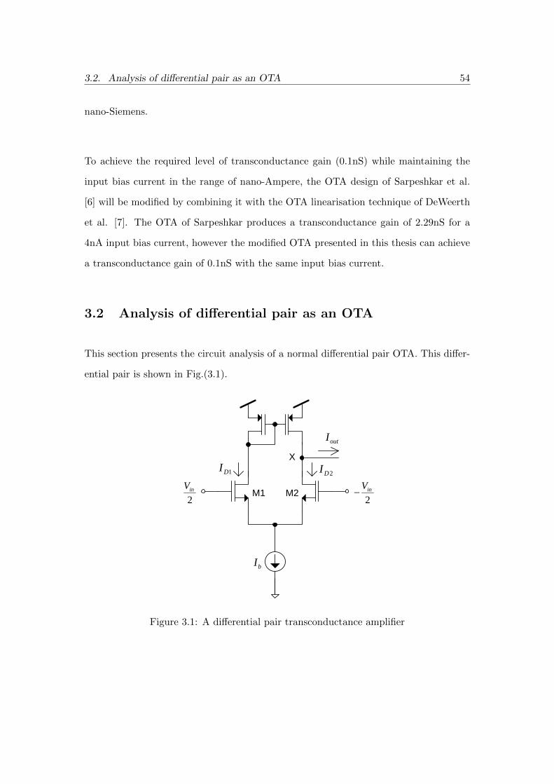
3.2. Analysis of differential pair as an OTA 54
nano-Siemens.
To achieve the required level of transconductance gain (0.1nS) while maintaining the
input bias current in the range of nano-Ampere, the OTA design of Sarpeshkar et al.
[6] will be modified by combining it with the OTA linearisation technique of DeWeerth
et al. [7]. The OTA of Sarpeshkar produces a transconductance gain of 2.29nS for a
4nA input bias current, however the modified OTA presented in this thesis can achieve
a transconductance gain of 0.1nS with the same input bias current.
3.2 Analysis of differential pair as an OTA
This section presents the circuit analysis of a normal differential pair OTA. This differ-
ential pair is shown in Fig.(3.1).
bI
outI
M1 M2
1DI 2DIX
2inV
2inV
Figure 3.1: A differential pair transconductance amplifier

3.2. Analysis of differential pair as an OTA 55
At node X, a KCL analysis gives:
ID1 = IOUT + ID2 (3.1)
When this differential pair is biased in the weak inversion region and all the transistors
are perfectly matched, the output current (IOUT ) is equal to:
IOUT = ID1 − ID2
= I0W
L
[exp(
V in
2)− exp(
−V in2
)] (3.2)
The relationship between Ib, ID1 and ID2 is:
Ib = ID1 + ID2
= I0W
L
[exp(
V in
2) + exp(
−V in2
)] (3.3)
The term ( IOUTIb) is a division of eq.(3.2) by (3.3). Thus:
IOUTIb
=I0WL
[exp( Vin
2nUT)− exp( −Vin2nUT
)]
I0WL
[exp( Vin
2nUT) + exp( −Vin2nUT
)]
=exp( Vin
2nUT)− exp( −Vin2nUT
)
exp( Vin2nUT
) + exp( −Vin2nUT)
= tanh(Vin
2nUT)
(3.4)
A Taylor’s series of tanh(x) is:

3.3. Analysis with signal flow graph technique 56
tanh(x) = x− x3
3+
2x5
15− 17x7
315+ ...+ (3.5)
Therefore, the Taylor’s series of tanh( Vin2nUT
) in eq.(3.4) is:
IOUT = Ib
(Vin
2nUT−
( Vin2nUT
)3
3+
2( Vin2nUT
)5
15−
17( Vin2nUT
)7
315+ ...+
)
≈( Ib
2nUT
)Vin
(3.6)
where Ib2nUT
is the transconductance gain of the differential pair.
3.3 Analysis with signal flow graph technique
Alternatively, the analysis of an OTA can be represented by a block diagram of the half
circuit and a signal flow graph as proposed by R. Sarpeshkar et al. [6]. First of all, let
us consider the equation for the drain current of a subthreshold MOSFET:
iDS = I0W
Lexp(
VGSnUT
) exp((n− 1)VBS
nUT) (3.7)
The transconductance of the gate, bulk and source are the derivatives of eq.(3.7):
ggate =∂iDS∂vG
=idsvg
=IDnUT
gbulk =∂iDS∂vB
=idsvb
= (n− 1
nUT)ID
gsource =∂iDS∂vS
=idsvs
=IDUT
(3.8)

3.3. Analysis with signal flow graph technique 57
Sarpeshkar also recommended that all small signal parameters should be dimensionless
(i = id/ID or v = vd/UT ), therefore id = gdvd = IDvd/nUT which simply is i = v/n.
In this case, n is considered as a dimensionless transconductance. From eq.(3.8), the
dimensionless transconductance of the gate, the bulk and the source are 1/n, (n− 1)/n
and 1, respectively. The small signal equivalent circuit and the signal flow graph of a
MOSFET are shown in Fig.(3.2(b)) and (3.2(c)), respectively.
SV
GVBV
DSi
DV
(a)
T
gsDS
nUVVI )(
T
bsDS
nUVVIn )()1(
dV
gV bVDSi
(b)
+n
n 1
n1
+-
-
1
bV
gV
sV
DSi
(c)
Figure 3.2: (a) A transistor with corresponding voltages and currents. (b) The small sig-nal equivalent circuit for the bulk transistor. (c) The signal flow graph of dimensionlessmodel for the bulk transistor.
An OTA with double source degeneration transistors is shown in Fig.(3.3). The equiv-
alent half circuit and signal flow graph are illustrated in Fig.(3.4(a)) and (3.4(b)), re-
spectively.
The dimensionless transconductance of the gate (1/n2) is attenuated by a feedback fac-
tor of the drain (n1) and the source (n3n4). The overall dimensionless transconductance
for this circuit is given by:
g =1/n2
1 + n1 + (n3n4)(3.9)

3.3. Analysis with signal flow graph technique 58
bI
outI
2inV
2inV
Figure 3.3: Differential pair as an OTA with double source degeneration
2inV
1
2
3
4
(a)
++
-
1
gV
sV
DSi1n
3n
4n
2
1n
(b)
Figure 3.4: (a) The half equivalent circuit of OTA in Fig.(3.3). (b) The signal flowgraph of Fig.(3.4(a))
Let n1 = np and n2 = n3 = n4 = nn. Thus, eq.(3.9) becomes:

3.3. Analysis with signal flow graph technique 59
g =1
nn(n2n + np + 1)
(3.10)
g is the dimensionless parameter with Ib2UT
as the multiplication factor to obtain the
actual transconductance. Therefore, the output current from this double source degen-
eration is:
Iout =Ib
2nn(n2n + np + 1)UT
Vin (3.11)
where the tranconductance gain (gm) in this case is Ib2nn(n2
n+np+1)UT. With Ib = 5nA,
nn = 1.3, np = 1.28 and UT = 25.82mV @ 300K, the theoretical gm for this circuit is
18.76nS. This calculation is confirmed by the Cadence simulation result (19.4nS), shown
in Fig.(3.5)
����
����
����
����
����
��� ��������������
�����������
���� ������������ ����� � ������!��
Figure 3.5: Simulation result for transconductance amplifier in Fig.(3.3)

3.4. Analysis of a bulk driven OTA with source degeneration and bump linearisation60
3.4 Analysis of a bulk driven OTA with source degenera-
tion and bump linearisation
To further reduce the transconductance gain and increase the linear range of the OTA,
R. Sarpeshkar et al. [6] demonstrated a circuit of the differential pair OTA with a bulk
input and bump linearisation [8]. This OTA circuit with two extra diode-connected
PMOS transistors is shown in Fig.(3.6).
outI
2inV
2inV
bI
B1
B2
MN1 MN2
Figure 3.6: Bulk differential pair as an OTA with double source degeneration
First, let’s consider the circuit without considering of the bump linearisation [8] tran-
sistors, shown in the shaded area, the half circuit of this OTA and its signal flow graph
are illustrated in Fig.(3.7(a)) and (3.7(b)), respectively. The dimensionless conductance
(g) for this case is given by:
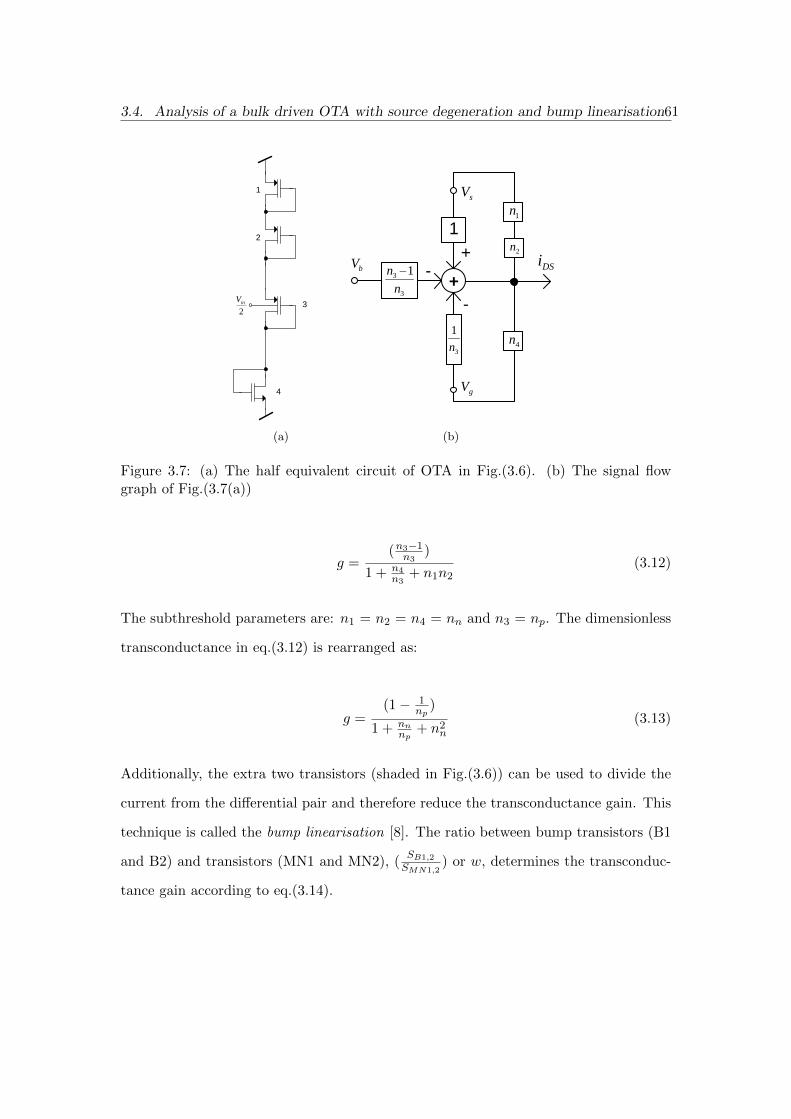
3.4. Analysis of a bulk driven OTA with source degeneration and bump linearisation61
2inV
1
2
3
4
(a)
inVinV
outI
1xI
2xI
bI
outI
M1 M2
1DI2DI
X
2
inV
2
inV
SV
GVBV
DSi
DV
T
gsDS
nU
VVI )(
T
bsDS
nU
VVIn )()1(
dV
gVbVDSi
+n
n 1
n
1
+-
-
1
bV
gV
sV
DSi
bI
outI
2
inV
2
inV
+
+
-
1
gV
sV
DSi
2
inV
1
2
3
4
1n
3n
4n
2
1
n
2
inV+
+-
-
1
bV
gV
sV
DSi
1
2
3
4
3
3 1
n
n
3
1
n 4n
2n
1n
outI
2
inV
2
inV
bI
B1
B2
MN1 MN2
+
+
-
1
gV
sV
DSi
2
inV
1
2
3
4
1n
3n
4n
2
1
n
inVinV
outI
1xI
2xI
inVinV
outI
1xI
2xI
6.5
6.5
35.0
100
6.5
2.67
35.0
200
6.5
6.5
6.5
6.5
6.5
6.5
6.5
2.67
35.0
100
35.0
100
35.0
100
35.0
100
35.0
100
35.0
200
35.0
200
35.0
200
35.0
200
35.0
200
35.0
200
35.0
200
6.5
6.5
6.5
6.5
inVinV
outI
1xI
2xI
6.5
6.5
35.0
100
6.5
2.67
35.0
200
6.5
6.5
6.5
6.5
6.5
6.5
6.5
2.67
35.0
100
35.0
100
35.0
100
35.0
100
35.0
100
35.0
200
35.0
200
35.0
200
35.0
200
35.0
200
35.0
200
35.0
200
6.5
6.5
6.5
6.5
N1
P1
N2 N4
N3
N5N6
N7 N8
N9 N10
N11 N12
N13 N14
P2
P3 P4
P5 P6
P7 P8
+
+-
-
1
gV
sV
DSi
2
inV 1
1 1
P
P
n
n
1
1
Pn2Nn
5Pn
3Pn
2
inV
P5
P3
P1
N2
2
inV
N13
N11
N9
N7
+
+
-
1
gV
sV
DSi
11
1
Nn
13Nn
9Nn
7Nn
(b)
Figure 3.7: (a) The half equivalent circuit of OTA in Fig.(3.6). (b) The signal flowgraph of Fig.(3.7(a))
g =(n3−1n3
)
1 + n4n3
+ n1n2(3.12)
The subthreshold parameters are: n1 = n2 = n4 = nn and n3 = np. The dimensionless
transconductance in eq.(3.12) is rearranged as:
g =(1− 1
np)
1 + nnnp
+ n2n
(3.13)
Additionally, the extra two transistors (shaded in Fig.(3.6)) can be used to divide the
current from the differential pair and therefore reduce the transconductance gain. This
technique is called the bump linearisation [8]. The ratio between bump transistors (B1
and B2) and transistors (MN1 and MN2), (SB1,2
SMN1,2) or w, determines the transconduc-
tance gain according to eq.(3.14).
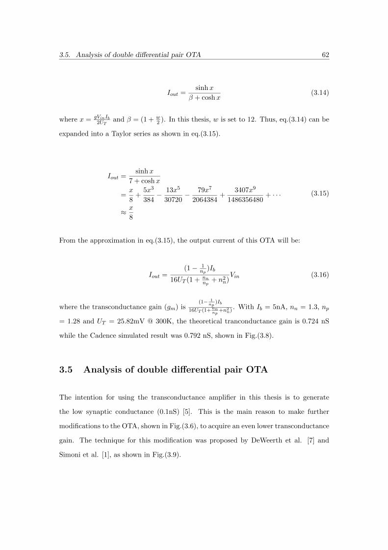
3.5. Analysis of double differential pair OTA 62
Iout =sinhx
β + coshx(3.14)
where x = gVinIb2UT
and β = (1 + w2 ). In this thesis, w is set to 12. Thus, eq.(3.14) can be
expanded into a Taylor series as shown in eq.(3.15).
Iout =sinhx
7 + coshx
=x
8+
5x3
384− 13x5
30720− 79x7
2064384+
3407x9
1486356480+ · · ·
≈ x
8
(3.15)
From the approximation in eq.(3.15), the output current of this OTA will be:
Iout =(1− 1
np)Ib
16UT (1 + nnnp
+ n2n)Vin (3.16)
where the transconductance gain (gm) is(1− 1
np)Ib
16UT (1+nnnp
+n2n)
. With Ib = 5nA, nn = 1.3, np
= 1.28 and UT = 25.82mV @ 300K, the theoretical tranconductance gain is 0.724 nS
while the Cadence simulated result was 0.792 nS, shown in Fig.(3.8).
3.5 Analysis of double differential pair OTA
The intention for using the transconductance amplifier in this thesis is to generate
the low synaptic conductance (0.1nS) [5]. This is the main reason to make further
modifications to the OTA, shown in Fig.(3.6), to acquire an even lower transconductance
gain. The technique for this modification was proposed by DeWeerth et al. [7] and
Simoni et al. [1], as shown in Fig.(3.9).
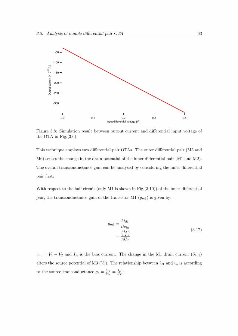
3.5. Analysis of double differential pair OTA 63
����
����
����
����
����
���
����� ������������
���������������
��� ����� ����� ������ ����
Figure 3.8: Simulation result between output current and differential input voltage ofthe OTA in Fig.(3.6)
This technique employs two differential pair OTAs. The outer differential pair (M5 and
M6) senses the change in the drain potential of the inner differential pair (M1 and M2).
The overall transconductance gain can be analysed by considering the inner differential
pair first.
With respect to the half circuit (only M1 is shown in Fig.(3.10)) of the inner differential
pair, the transconductance gain of the transistor M1 (gm1) is given by:
gm1 =δid1
∂vin
=
(IA2
)nUT
(3.17)
vin = V1 − V2 and IA is the bias current. The change in the M1 drain current (∂id1)
alters the source potential of M3 (V5). The relationship between id1 and v5 is according
to the source tranconductance gs = δidδvs
= IDUT
:
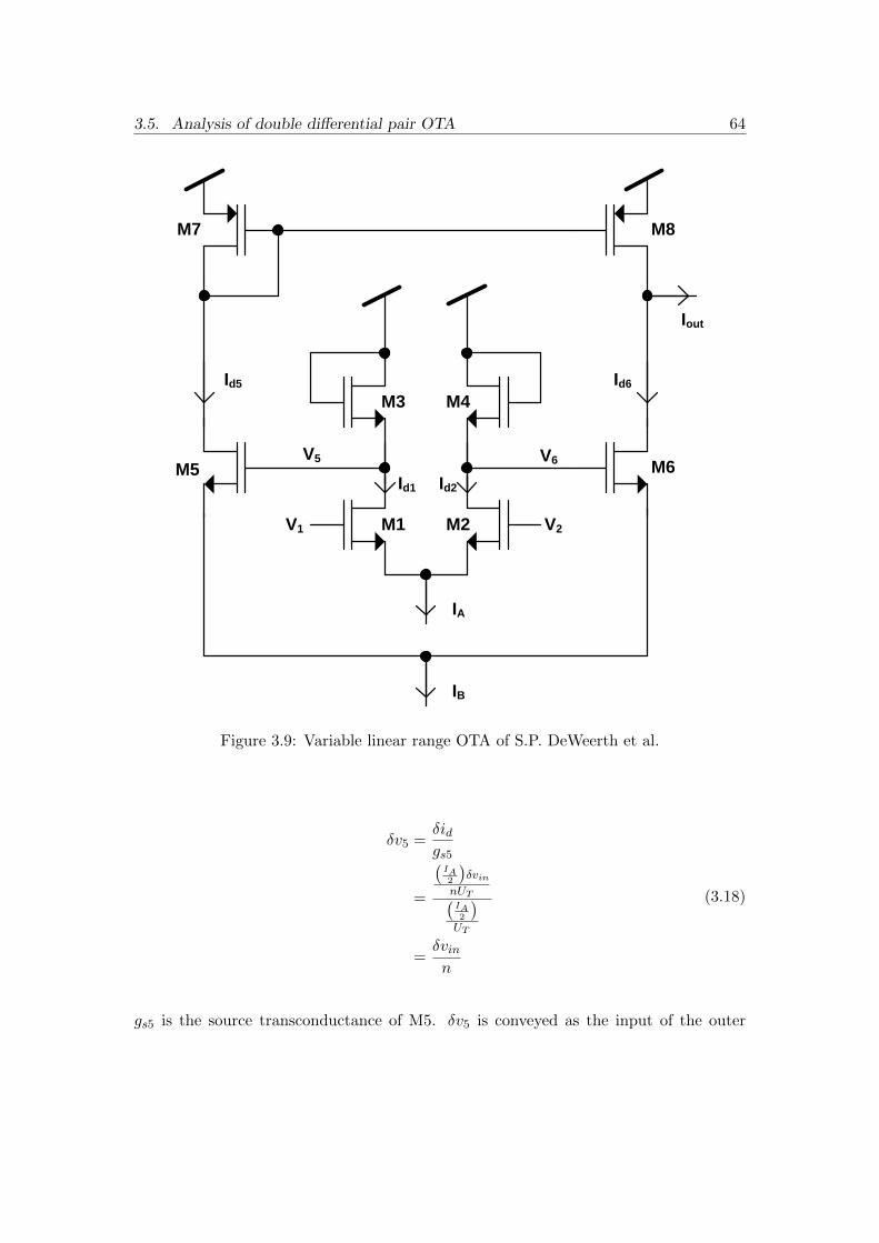
3.5. Analysis of double differential pair OTA 64
M1 M2
M3 M4
M5
M7 M8
M6
V1 V2
Id1 Id2
Id5 Id6
Iout
IA
IB
V5 V6
Figure 3.9: Variable linear range OTA of S.P. DeWeerth et al.
δv5 =δidgs5
=
(IA2
)δvin
nUT(IA2
)UT
=δvinn
(3.18)
gs5 is the source transconductance of M5. δv5 is conveyed as the input of the outer
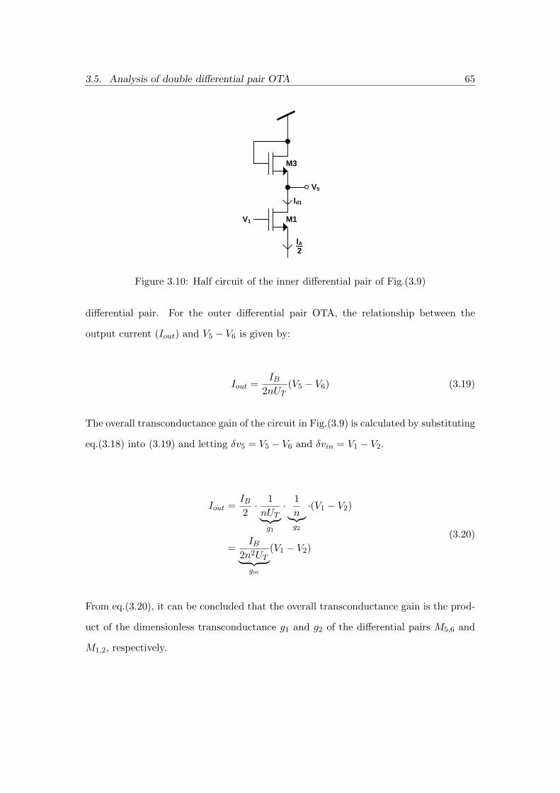
3.5. Analysis of double differential pair OTA 65
M1
M3
V1
Id1
V5
IA2
Figure 3.10: Half circuit of the inner differential pair of Fig.(3.9)
differential pair. For the outer differential pair OTA, the relationship between the
output current (Iout) and V5 − V6 is given by:
Iout =IB
2nUT(V5 − V6) (3.19)
The overall transconductance gain of the circuit in Fig.(3.9) is calculated by substituting
eq.(3.18) into (3.19) and letting δv5 = V5 − V6 and δvin = V1 − V2.
Iout =IB2· 1
nUT︸ ︷︷ ︸g1
· 1
n︸︷︷︸g2
·(V1 − V2)
=IB
2n2UT︸ ︷︷ ︸gm
(V1 − V2)
(3.20)
From eq.(3.20), it can be concluded that the overall transconductance gain is the prod-
uct of the dimensionless transconductance g1 and g2 of the differential pairs M5,6 and
M1,2, respectively.

3.5. Analysis of double differential pair OTA 66
Using the similar topology as the circuit shown in Fig.(3.9), the equivalent transconduc-
tance gain of the OTA in Fig.(3.11) can be calculated in the same regime. On the LHS
of Fig.(3.11) is the bulk driven OTA, analysed in the previous section, and on the RHS
(shaded) is the NMOS differential pair OTA with double source degeneration transis-
tors. The other two transistors on top of the RHS differential pair are diode-connected
MOSFETs, which act as the load. The half circuit and signal flow graph diagram of
the shaded OTA are shown in Fig.(3.12(a)) and (3.12(b)), respectively.
inVinV
outI
1xI
2xI
bI
outI
M1 M2
1DI2DI
X
2
inV
2
inV
SV
GVBV
DSi
DV
T
gsDS
nU
VVI )(
T
bsDS
nU
VVIn )()1(
dV
gVbVDSi
+n
n 1
n
1
+-
-
1
bV
gV
sV
DSi
bI
outI
2
inV
2
inV
+
+
-
1
gV
sV
DSi
2
inV
1
2
3
4
1n
3n
4n
2
1
n
2
inV
1
2
3
4
outI
2
inV
2
inV
bI
B1
B2
MN1 MN2
+
+
-
1
gV
sV
DSi
2
inV
1
2
3
4
1n
3n
4n
2
1
n
inVinV
outI
1xI
2xI
inVinV
outI
1xI
2xI
6.5
6.5
35.0
100
6.5
2.67
35.0
200
6.5
6.5
6.5
6.5
6.5
6.5
6.5
2.67
35.0
100
35.0
100
35.0
100
35.0
100
35.0
100
35.0
200
35.0
200
35.0
200
35.0
200
35.0
200
35.0
200
35.0
200
6.5
6.5
6.5
6.5
inVinV
outI
1xI
2xI
6.5
6.5
35.0
100
6.5
2.67
35.0
200
6.5
6.5
6.5
6.5
6.5
6.5
6.5
2.67
35.0
100
35.0
100
35.0
100
35.0
100
35.0
100
35.0
200
35.0
200
35.0
200
35.0
200
35.0
200
35.0
200
35.0
200
6.5
6.5
6.5
6.5
N1
P1
N2 N4
N3
N5N6
N7 N8
N9 N10
N11 N12
N13 N14
P2
P3 P4
P5 P6
P7 P8
+
+-
-
1
gV
sV
DSi
2
inV 1
1 1
P
P
n
n
1
1
Pn2Nn
5Pn
3Pn
2
inV
P5
P3
P1
N2
2
inV
N13
N11
N9
N7
+
+
-
1
gV
sV
DSi
11
1
Nn
13Nn
9Nn
7Nn
+
+
-
-
1
bV
gV
sV
DSi
3
3 1
n
n
3
1
n 4n
2n
1n
+
+-
-
1
bV
gV
sV
DSi
3
3 1
n
n
3
1
n 4n
2n
1n
Figure 3.11: The double differential pair OTA

3.5. Analysis of double differential pair OTA 67
2inV
1
2
3
4
(a)
++
-
1
gV
sV
DSi1n
3n
4n
2
1n
(b)
Figure 3.12: (a) The half equivalent circuit of OTA in Fig.(3.11). (b) The signal flowgraph of Fig.(3.12(a))
From the signal flow graph in Fig.(3.12(b)), the dimensionless transconductance of the
OTA on the RHS is:
gRHS =1n2
1 + n1 + n3n4(3.21)
where n1, n2, n3 and n4 are the weak inversion slope of the transistor 1, 2, 3 and 4,
respectively. In this case all transistors are NMOS, eq.(3.21) can be rewritten as:
gRHS =1
nn(n2n + nn + 1)
(3.22)
For the complete OTA circuit in Fig.(3.11), the output current is:

3.5. Analysis of double differential pair OTA 68
Iout =gLHSgRHSIx1
2UT(Vin+ − Vin−)
=(1− 1
np)Ix1
nn(1 + nnnp
+ n2n)(n2
n + nn + 1)16UT(Vin+ − Vin−)
(3.23)
where(1− 1
np)Ix1
nn(1+nnnp
+n2n)(n2
n+nn+1)16UTis the transconductance gain. With Ix1 = 5nA, nn
= 1.3, np = 1.28 and UT = 25.82mV @ 300K, the theoretical gm for this circuit is
1.3968×10⁻¹⁰ S. This is confirmed by the simulation result, shown in Fig.(3.13), where
the obtained tranconductance gain was 1.2615×10⁻¹⁰ S. It should be noted that the
tranconductance gain is independent of Ix2 when the RHS differential pair is operated
in the subthreshold region [7].
��
��
��
�
���
��������� �����������
���������������
� �� ������� ���� ������� ����
Figure 3.13: Simulation result between output current and differential input voltage ofthe OTA in Fig.(3.11)
The important parameters of each transconductance design are summarised in Table
(3.1).

3.6. Summary 69
Table 3.1: Important parameters of each OTAs designOTA topology Linear range Transistor count Theoretical dimensionless gm
A differential pair in Fig.(3.1) 60mV 4 0.769
A differential pair with two source degenera-tion in Fig.(3.3)
260mV 8 0.193
DeWeerth et al. [7] (Fig.(3.9)) 3V 8 0.591
Sarpeshkar et al. [6] (Fig.(3.6)) 3.4V 14 0.00747
The OTA proposed in this work (Fig.(3.11)) 2.5V 22 0.00143
3.6 Summary
In this chapter, the analysis and the design of a low gain transconductance amplifier
have been presented. A traditional differential pair OTA operated in the weak inversion
region was described and analysed. The transconductance gain, a hyperbolic function
is transformed into a Taylor series.
The circuit analysis technique called signal flow graph [6] was explained with a circuit
analysis example. This technique is useful for analysing complex OTA topologies. A
differential pair with a MOSFET body input was introduced to decrease the transcon-
ductance gain and increase the linear range. Furthermore, the analysis of the source
degeneration and the bump linearisation techniques was presented.
At the end of this chapter, the final double differential pair OTA design was analysed.
This OTA combined all the previously mentioned design techniques and was able to
decrease the transconductance gain to the range of sub-nano Siemens (0.1nS for a 3.6nA
bias current).

References
[1] M. F. Simoni, G. S. Cymbalyuk, M. E. Sorensen, R. L. Calabrese, and S. P. De-
Weerth, “A multiconductance silicon neuron with biologically matched dynamics,”
Biomedical Engineering, IEEE Transactions on, vol. 51, no. 2, pp. 342–354, Feb.
2004.
[2] E. M. Drakakis, A. J. Payne, and C. Toumazou, “Log-domain state-space: a sys-
tematic transistor-level approach for log-domain filtering,” Circuits and Systems II:
Analog and Digital Signal Processing, IEEE Transactions on, vol. 46, no. 3, pp.
290–305, 1999.
[3] E. Lazaridis and E. M. Drakakis, “Full analogue electronic realisation of the hodgkin-
huxley neuronal dynamics in weak-inversion cmos,” in Engineering in Medicine and
Biology Society, 2007. EMBS 2007. 29th Annual International Conference of the
IEEE, 2007, pp. 1200–1203.
[4] P. Georgiou and C. Toumazou, “A silicon pancreatic beta cell for diabetes,” Biomed-
ical Circuits and Systems, IEEE Transactions on, vol. 1, no. 1, pp. 39–49, 2007.
[5] Z. F. M. Alain Destexhe and T. J. Sejnowski, Kinetic models of synaptic transmis-
sion., 2nd ed., ser. Methods in Neuronal Modeling (2nd ed.). Cambridge, MA: MIT
Press, 1998, pp. 1–26.
70

REFERENCES 71
[6] R. Sarpeshkar, R. F. Lyon, and C. Mead, A low-power wide-linear-range transcon-
ductance amplifier, ser. Neuromorphic Systems Engineering: Neural Networks in
Silicon. Norwell, MA, USA: Kluwer Academic Publishers, 1998, pp. 267–313.
[7] S. P. DeWeerth, G. N. Patel, and M. F. Simoni, “Variable linear-range subthreshold
OTA,” Electronics Letters, vol. 33, no. 15, pp. 1309–1311, 1997.
[8] T. Delbruck, “‘bump’ circuits for computing similarity and dissimilarity of analog
voltages,” in Neural Networks, 1991., IJCNN-91-Seattle International Joint Confer-
ence on, vol. i, 1991, pp. 475–479 vol.1.
Chapter 4
ISFET and Iontophoresis
Technique
4.1 Introduction
The most important element in the bionics chemical synapse is the chemical front-end;
the neurotransmitter sensor. The purpose of this sensor is to function as the receptor
of the chemical synapse i.e. to detect the presence of the neurotransmitter. As the
processing circuit, used to duplicate the biological functionality, will be implemented
using CMOS technology, therefore the sensor for this chemical synapse should also be
integrable on the same platform. The ISFET has demonstrated its ability to function
as the chemical sensor for this work [1].
In this chapter, the principle of an ISFET will be described in terms of its chemical
and mathematical theory. The ISFET’s operation, sensitivity and drift will also be
presented. Additionally, the enzyme-modified ISFET will be introduced as the broad-
72

4.2. ISFET principle 73
specific chemical sensor due to its capability to sense different chemical species. The
glutamate ISFET, that will emulate the function of the AMPA and NMDA receptors
in the bionics chemical synapse, will be studied and implemented from a commercially-
available ISFET.
The second part of this chapter will discuss a fast chemical stimulus technique that
will be used to reproduce the neurotransmitter signal. The required one-millisecond
chemical perturbation is fulfilled by a technique called iontophoresis. Experimental
result shows that this technique can generate a fast chemical stimulus with the desired
time duration.
4.2 ISFET principle
The origin of an ion-sensitive field effect transistor (ISFET) can be traced back to the
1970s with the main contribution made by Piet Bergveld. Initially, the purpose of this
compact solid-state chemical sensor was to act as the probe for the monitoring of ionic
activities in both electrochemical and biological systems [2]. Since then, the research
group at Twente University has published a number of in-depth reports on the charac-
teristics of the ISFET and its applications. The operation and principle of ISFETs and
MOSFETs are similar. An ISFET is a floating gate MOSFET with an extra insulating
membrane. In the case of a MOSFET, its operational regions are determined by its bias
potential at the gate while an ISFET requires a reference electrode (Ag/AgCl) as its
pseudo-gate for biasing. The change in pH alters the threshold voltage of the ISFET,
which can be sensed through the drain current or the gate source potential.
The applications of the ISFET are mainly about pH sensing. However, there have been

4.2. ISFET principle 74
extensive use of ISFETs to sense different chemical species, such as glucose [3], urea [4],
glutamate [5], creatine [6], acetylcholine [7], γ-aminobutyric acid [8]. The detection of
these solutions is carried out by the immobilisation of certain enzymes on top of the
gate of the ISFET, called an ENFET. The immobilised enzyme catalyses a chemical
reaction with the interested analyte and the product of this reaction can be H+ or OH–,
altering the local pH at the membrane layer of the ENFET.
4.2.1 ISFET Operation
To understand how an ISFET operates, it is important to analyse the working mecha-
nisms of a MOSFET. The planar cross section of an ISFET is shown in Fig.(4.1). This
diagram is similar to a MOSFET structure with the exception that the gate terminal is
floating and requires a reference electrode for biasing. In the case of the MOSFET, the
current channel through the drain and source is controlled by the gate voltage. In other
words, the gate voltage modulates this channel and the source-drain path is blocked
where there is no gate bias. However, when the voltage bias at the gate is below the
threshold voltage, an exponential relationship between the drain current and the gate
potential is observed. Furthermore, if the gate potential is higher than the threshold
voltage, this relationship becomes either linear in the triode region or square in the
saturation region.
For the ISFET, both the floating gate voltage (biased via the reference electrode) and
the pH of the solution determines the drain current. The effect of the solution’s pH on
the drain current of the ISFET is illustrated in Fig.(4.2). The threshold voltage of an
ISFET (Vth(ISFET )) can be expressed in terms of the threshold voltage of a MOSFET
(Vth(MOSFET )) and the grouping of the pH dependent potentials (Vchem), as shown in
eq.(4.1).

4.2. ISFET principle 75
n+n+p+
G
DSB
p-type Si
Insulatingmembrane
SiO2
Figure 4.1: Ion Sensitive Field Effect Transistor
Vth(ISFET ) = Vth(MOSFET ) + Vchem
= Eref − ψs + xsol −φmq
+ Vth(MOSFET )
(4.1)
Vchem = Eref − ψs + xsol −φmq
(4.2)
From eq.(4.1), Eref is the bias potential of the reference electrode, ψs is a pH dependent
chemical potential, xsol is the surface dipole potential of the solution and φmq is the metal
work function. The pH sensitivity of the ISFET or the relationship between Vchem, in
eq.(4.2), and the pH can be explained with the site-binding theory and the double layer
theory.
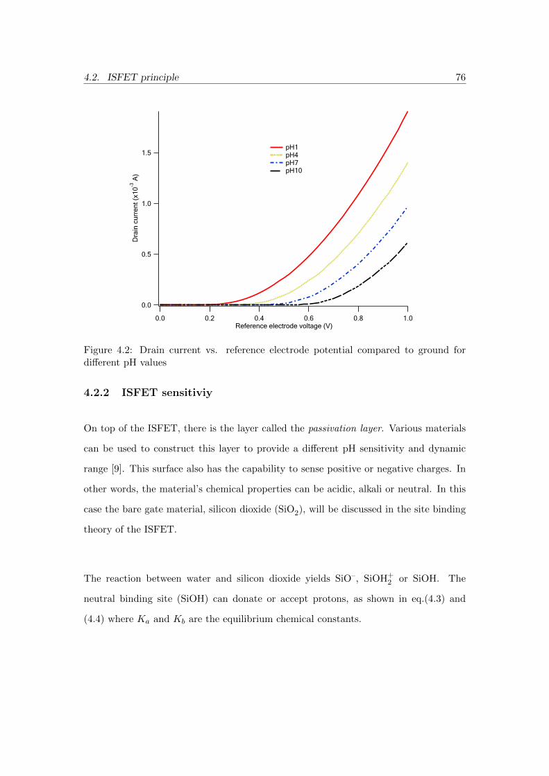
4.2. ISFET principle 76
���
���
���
���
�������� ��������
������������������������� ��� ���� ��� ��� ���
!� !� !" !��
Figure 4.2: Drain current vs. reference electrode potential compared to ground fordifferent pH values
4.2.2 ISFET sensitiviy
On top of the ISFET, there is the layer called the passivation layer. Various materials
can be used to construct this layer to provide a different pH sensitivity and dynamic
range [9]. This surface also has the capability to sense positive or negative charges. In
other words, the material’s chemical properties can be acidic, alkali or neutral. In this
case the bare gate material, silicon dioxide (SiO2), will be discussed in the site binding
theory of the ISFET.
The reaction between water and silicon dioxide yields SiO–, SiOH+2 or SiOH. The
neutral binding site (SiOH) can donate or accept protons, as shown in eq.(4.3) and
(4.4) where Ka and Kb are the equilibrium chemical constants.
4.2. ISFET principle 77
SiOH −−⇀↽−− SiO− + H+S with Ka =
[SiO−][H+]s[SiOH]
(4.3)
SiOH + H+S−−⇀↽−− SiOH+
2 with Kb =[SiOH+
2 ]
[SiOH][H+]s(4.4)
To find the ability of silicon dioxide to resist a change in pH, the buffer capacity pa-
rameter (β) is defined as:
β =d[B]
dpHs(4.5)
where [B] is the total surface charge which is [SiO–]+[SiOH+2 ] and pHs is the pH at the
SiO2 surface. This total surface charge can be determined from the ratio between the
surface charge density and the charge [10], defined as:
[B] =−σsq
(4.6)
The surface charge density is modelled as two layers which are the Stern inner layer and
the outer diffuse layer [11, 12]. The positive and negative ions in the solution between
the gap of these layers form the equivalent capacitor. The relationship between this
double layer capacitance (Cdl) and σs is:
σs = ψsCdl (4.7)
ψs is the electrical surface potential. Substituting eq.(4.7) into eq.(4.6):
4.2. ISFET principle 78
[B] =−1
q(ψsCdl) (4.8)
Substitute eq.(4.8) into eq.(4.5):
β =d(−ψsCdlq )
dpHs
=−Cdlq
dψsdpHs
(4.9)
Rearrange eq.(4.9):
dψsdpHs
=−qβCdl
(4.10)
According to the Boltzmann equation, the concentration of hydrogen ions at the surface
[H+s ] and the bulk concentration of hydrogen ions [H+] is given by:
[H+s ] = [H+] exp(
−qψsKT
) (4.11)
Rearrange eq.(4.11) by substituting [H+s ] = 10-pHs and [H+] = 10-pH:
−qψskT
= ln[10(-pHs+pH)]
ψs = (ln 10)kT
q(pHs − pH)
(4.12)
Differentiate eq.(4.12) with respect to pH:

4.2. ISFET principle 79
dψsdpH
= (ln 10)kT
q
(dpHs
dpH− 1
)(4.13)
Substitute dpHsdpH = dpHs
dψs× dψs
dpH into eq.(4.13):
dψsdpH
= 2.3kT
q
[(dpHs
dψs× dψs
dpH
)− 1
]−2.3
kT
q=
dψsdpH
(1− 2.3
kT
q
dpHs
dψs
)dψsdpH
=2.3kTq
2.3kTqdpHsdψs− 1
(4.14)
Substitute eq.(4.10) into eq.(4.14):
dψsdpH
=2.3kTq
2.3kTq (−Cdlqβ )− 1
=−2.3kTq
2.3kTq (Cdlqβ ) + 1
= −2.3αUT
(4.15)
where α is the sensitivity coefficient = 1
2.3 kTq
(Cdlqβ
)+1and UT is the thermal voltage = kT
q .
When α reaches unity, this sensitivity will be 59mV/pH at 300K. The pH sensitivity
when α = 1 is defined as the Nernstian sensitivity.
From eq.(4.15), it can be realised that dψs = −2.3αUTdpH or ψs = −2.3αUTpH. With
the substitution of this term to eq.(4.2), the simplified expression [13] for Vchem is:

4.2. ISFET principle 80
Vchem = γ +2.3αkT
qpH (4.16)
where γ is the grouping of the non-pH terms. From eq.(4.15), it can be observed that
the buffer capacity for the sensing area of the ISFET is a crucial parameter to deter-
mine its pH sensitivity. A material with a higher buffer capacity provides a greater level
of sensitivity. Amongst the common materials used for the ISFET’s passivation layer,
Ta2O5 gives the highest pH sensitivity owing to its high buffer capacity [14].
A study was conducted to try to provide a pH sensitivity higher than that of the
Nernstian relationship. By adding a chemical, NaF, into the solution [15], the sensitivity
increased to 80-85 mV/pH. However, the dynamic range for this modification is narrow
(in the range of pH 4-6).
4.2.3 Reference electrode
Measurements in electrochemistry made by chemical sensors require a stable potential
as the reference point. This is achieved using a reference electrode, which provides both
a constant potential and an electrical interlink. To comply with this requirement, a
silver-silver chloride common reference electrode is typically used. Fig.(4.3) shows the
physical appearance of this electrode.
To provide a constant potential, the silver wire, coated with silver chloride, will be sub-
merged into a saturated sodium chloride solution (typically 3M). The electrical path is
provided through the porous glass (frit). This glass allows an electrical link to be made
but obstructs any chemical activities between the inside and outside of the electrode.

4.2. ISFET principle 81
Y
Ag – AgCl wire
Porous Glass (Frit) Saturate KCl
Figure 4.3: Ag-AgCl reference electrode
Also, the other function of this frit is to ensure that there is no any mix up between
saturated KCl solution inside the reference electrode and outside measured solution.
This separation between the measured solution and the KCl solution in the frit keeps
the potential of the Ag-AgCl electrode constant.
Another type of reference electrode, where there is no liquid junction between the ref-
erence wire and the environmental solution, is a pseudo reference electrode. Without
the reference electrode, the electrical potential of this reference electrode is uncertain.
Practical use of the pseudo reference electrode requires a more complex measurement
system. For example, a research group at Twente University under Bergveld employed
two ISFETs for measurements with a pseudo reference electrode [16]. One was desig-
nated as the measurement ISFET while the other acted as the reference. To obtain
the correct electrochemical signal, differentiation between these two ISFET signals was
required.
4.2. ISFET principle 82
Another interesting development in this area is the introduction of a micro reference
electrode. In 2003, Huang et al. fabricated a miniature Ag-AgCl reference electrode
[17]. However, this micro reference electrode cannot be integrated using a standard
CMOS process. Lastly, the integrated reference electrode approach was initiated by
Comte et al. in 1978 [18], where another ISFET (REFET) is used as a reference to a
measurement ISFET. However, it is difficult to fabricate a fully matched REFET and
ISFET.
4.2.4 Drift in ISFET
One of the non-ideal behaviours that can be found in an electrochemical sensor is the
increase or decrease in the measured signal when there is no actual change in the chemi-
cal concentration. This slow and uni-directional change is called drift. Drift is classified
into two categories: short- and long-term. Changes of a few mV per hour when an
ISFET has been in contact with the chemical solution for a few hours are considered as
the short-term drift [19]. A drift is considered to be a long-term drift when an ISFET
has been measuring for at least ten hours; furthermore, this change in the measured
signal could possibly be ten times more than in the short-tem drift case [19].
The method for the deposition of the sensing material on an ISFET was reported as
one of the factors that affect drift in ISFETs. Hammond et al. reported that drift in his
CMOS ISFET is higher than the post-processed ISFET [20]. His report also explained
and compared the physical difference in the material between a CMOS and a non-CMOS
ISFET. The plasma enhanced chemical vapour (PECVD) deposition method used in
CMOS ISFET is a lower temperature process, which produces non-uniform crystals or
a polycrystalline. On the other hand, a non-CMOS ISFET’s sensing membrane is grown
in a low pressure/high temperature condition which yields a single crystal.

4.3. Enzyme-Immobilised ISFET 83
There have been many attempts to compensate for drift in an ISFET. All of the drift
reduction schemes employed additional electronic circuits to counteract the drift in the
signal. This method requires an accurate drift model of the ISFET. However, the drift
effect in an ISFET can be neglected if the measurement time duration is less than a
minute. This means that a millisecond range chemical perturbation in the experiment
of this work will not be affected by both long or short term drift.
4.3 Enzyme-Immobilised ISFET
Typically, an ISFET is designed for pH sensing or the detection of a change in hydrogen
concentration. However, the function of an ISFET is not only limited to pH sensing.
There have been many research works that applied ISFETs as a broad-specific chemical
sensor, through extra modifications and post-processesing. An ISFET deposited with
an ion-selective membrane, which makes it sensitive to a specific ion, is classified as a
CHEMFET.
As mentioned earlier in section 4.2, an ISFET with an extra enzyme layer on top of
the sensing membrane is called EnFETs. The function of this enzyme is to catalyse
the chemical reaction to either yield extra protons or electrons. This means that the
EnFET measures the ions that are generated as a by-product of the hydrolysis reaction.
The first EnFET publication was made by Caras et al. in 1980 [21], where he proposed
an EnFET for sensing penicillin. Their penicillin-FET was coated with penicillinase.
An example of an EnFET that will be described here is the EnFET for detecting urea
[22].

4.3. Enzyme-Immobilised ISFET 84
Urea + 3 H2OUREASE−−−−−−→ CO2 + 2 NH+
4 + 2 OH− (4.17)
From eq.(4.17), when urea is hydrolysed with urease as the catalyst, this chemical re-
action will give extra OH– ions. The increase in OH– ions leads to a pH change which
can be sensed by the EnFET. Table (4.1) summarises the common analytes that can be
sensed with an ISFET.
Table 4.1: Common analytes and immobilised enzymes used in EnFETAnalyte Immobilised enzyme Local pH change Reference
Penicillin Penicillinase decrease [21]Glucose Glucose oxidase decrease [23]Lactate Lactate oxidase decrease [24]
Urea Urease increase [22]Creatinine Creatinine deiminase decrease [25]Glutamate Glutamate oxidase decrease [26]
γ-Aminobutyric acid GABA oxidase decrease [27]Acetylcholine Acetylcholine esterase decrease [28]
Caras also reported an interesting observation regarding the relationship between the
penicillin-FET’s linear range and sensitivity with the buffer capacity of the analyte. In
this experiment, it was observed that the Penicillin-ISFET tested in a higher concen-
tration buffer solution had a broader linear range and a lower sensitivity. In contrast,
the same EnFET gave a shorter linear range and a higher sensitivity when operated in
a lower concentration buffer solution.
4.3.1 Glutamate ISFET
According to the Destexhe’s chemical synapse model [29] on the AMPA and NMDA
receptors, the bionics version of these receptors requires a glutamate sensor as the

4.3. Enzyme-Immobilised ISFET 85
chemical input. The glutamate ISFETs used in this work are the Sentron ISFETs
(Sentron BV, the Netherlands) with glutamate oxidase (GLOD) immobilisation. The
chemical reaction of glutamate, catalysed by GLOD, is expressed as:
Glutamate + O2 + H2OGLOD−−−−→ 2− oxoglutarate + NH+
4 + H2O2
The procedures for this immobilisation follow Braeken et al.’s work [26]. The procedures
undertaken to achieved GLOD immobilisation are as follows:
� The ISFET’s surface was cleaned with a 3:1 solution of sulfuric acid and hydrogen
peroxide for 15 minutes.
� The cleaned ISFET was further treated in a UV/ozone machine for 15 minutes.
� After the UV/Ozone treatment, the ISFET was rinsed with ethanol.
� The ISFET was heated at 110◦C for 30 minutes on a hot plate.
� The ISFET was immersed in a 1:1 solution of Poly-l-lysine (PLL) solution (PLL
4mg/mL in 10mM borate buffer pH8) and sodium cynaoborohydride (NaCNBH3)
for 30 minutes.
� The ISFET was further immersed in a 1:1 V/V solution of glutaraldehyde solution
(GA) and NaCNBH3 for 30 minutes.
� GLOD coupling on the ISFETs surface was accomplished by using a pipette to
drop a 300µg/mL GLOD in PBS solution on the ISFET’s surface. The time
duration for this process was overnight.
� The overnight GLOD-coupled ISFETs was further treated with CNBH for 30
minutes.

4.3. Enzyme-Immobilised ISFET 86
The second treatment of the ISFETs with CNBH after GLOD coupling is vital for a
robust linkage of GLOD [26]. Also, it is advised that these glutamate ISFETs should
be kept at 4◦C with a Tris buffer (150mM) inside a light tight container [26].
For the bionics chemical synapse, a linear relationship between the ion concentration and
the output signal is required. However, a typical voltage-mode ISFET readout circuit
[30] has a logarithmic relationship. Five different concentration of HCl (0.5, 1, 1.5, 2
and 2.5mM) were tested with this ISFET readout circuit. The obtained calibration
curve, shown in Table 4.2 and Fig.(3.6), exhibits a logarithmic relationship.
Table 4.2: Data of the measured results for different HCl concentration of 0.5, 1, 1.5, 2and 2.5mM from a voltage-mode readout circuit [30]
HCL concentration (mM) Output voltage (mV)
0.5 -789.11 -770.5
1.5 -763.32 -757.2
2.5 -748.5
This readout circuit was operated in a dual supply ±6V and the reference electrode was
biased at 0V. This logarithmic curve can be linearised with the H-cell current mode
readout circuit, shown in Fig.(4.5), proposed by Shepherd et al. [31].
In Fig.(4.5), the ISFET current (IISFET ) is the square root function of the ions con-
centration. The relationship between IISFET and I1 [31] is:
IISFET = I1[IONS]0.5e−γnUT e
−VrefUT (4.18)
The translinear loop on transistors P1, P2, P3 and P4 functions as a current squarer.
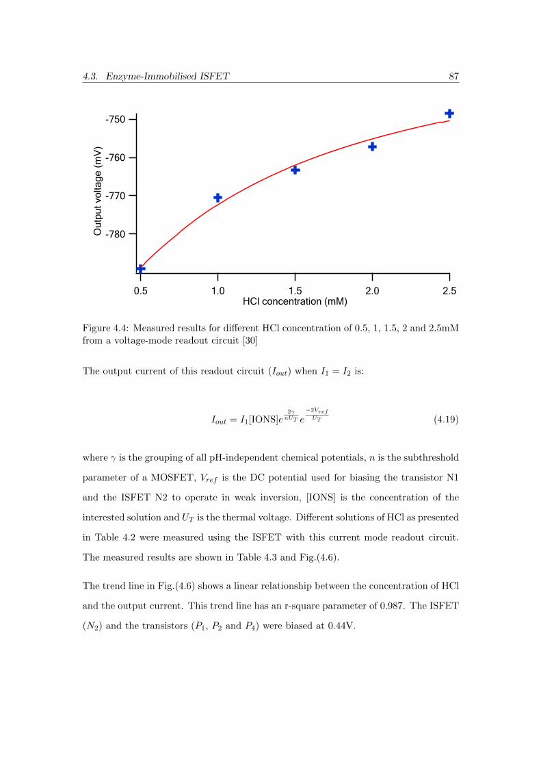
4.3. Enzyme-Immobilised ISFET 87
����
����
����
����
���� ������
��
������������������ � ������� � ����
Figure 4.4: Measured results for different HCl concentration of 0.5, 1, 1.5, 2 and 2.5mMfrom a voltage-mode readout circuit [30]
The output current of this readout circuit (Iout) when I1 = I2 is:
Iout = I1[IONS]e2γnUT e
−2VrefUT (4.19)
where γ is the grouping of all pH-independent chemical potentials, n is the subthreshold
parameter of a MOSFET, Vref is the DC potential used for biasing the transistor N1
and the ISFET N2 to operate in weak inversion, [IONS] is the concentration of the
interested solution and UT is the thermal voltage. Different solutions of HCl as presented
in Table 4.2 were measured using the ISFET with this current mode readout circuit.
The measured results are shown in Table 4.3 and Fig.(4.6).
The trend line in Fig.(4.6) shows a linear relationship between the concentration of HCl
and the output current. This trend line has an r-square parameter of 0.987. The ISFET
(N2) and the transistors (P1, P2 and P4) were biased at 0.44V.
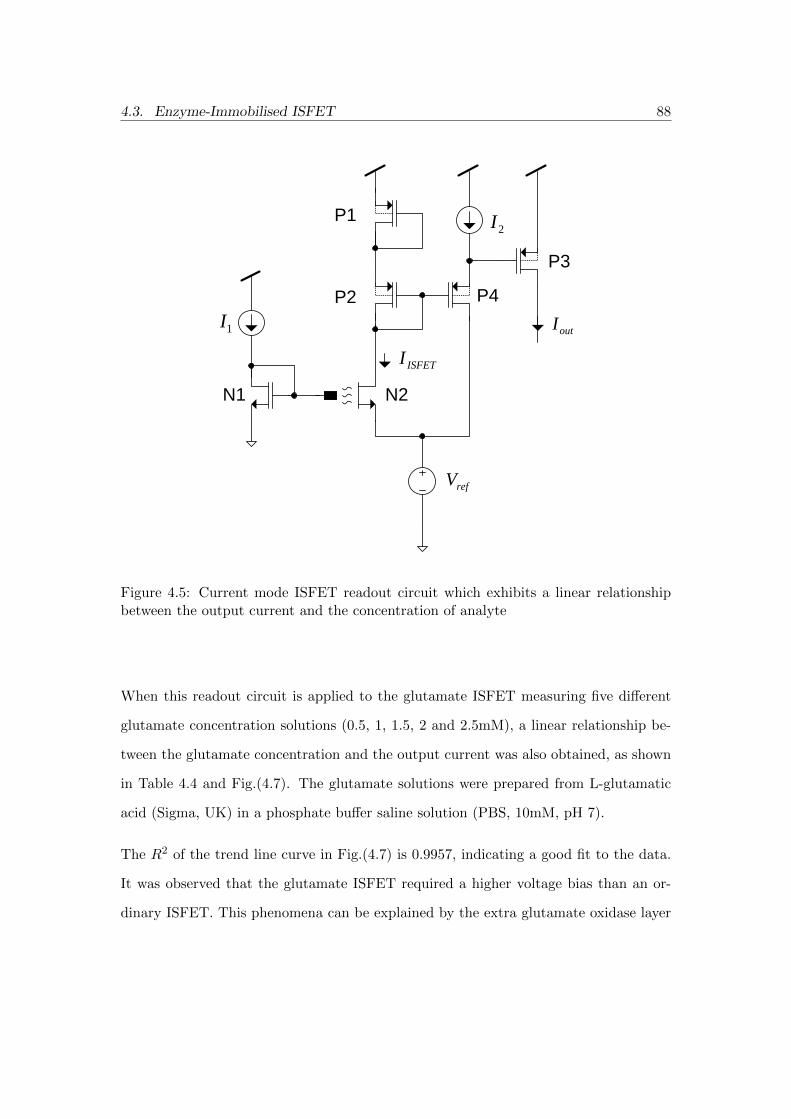
4.3. Enzyme-Immobilised ISFET 88
Y
refV
1I
2I
outI
N1 N2
P1
P2
P3
P4
ISFETI
Figure 4.5: Current mode ISFET readout circuit which exhibits a linear relationshipbetween the output current and the concentration of analyte
When this readout circuit is applied to the glutamate ISFET measuring five different
glutamate concentration solutions (0.5, 1, 1.5, 2 and 2.5mM), a linear relationship be-
tween the glutamate concentration and the output current was also obtained, as shown
in Table 4.4 and Fig.(4.7). The glutamate solutions were prepared from L-glutamatic
acid (Sigma, UK) in a phosphate buffer saline solution (PBS, 10mM, pH 7).
The R2 of the trend line curve in Fig.(4.7) is 0.9957, indicating a good fit to the data.
It was observed that the glutamate ISFET required a higher voltage bias than an or-
dinary ISFET. This phenomena can be explained by the extra glutamate oxidase layer
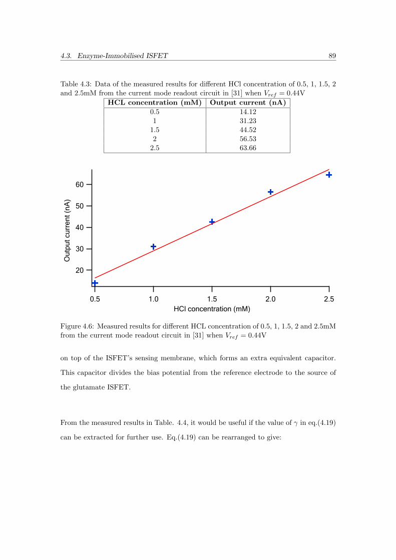
4.3. Enzyme-Immobilised ISFET 89
Table 4.3: Data of the measured results for different HCl concentration of 0.5, 1, 1.5, 2and 2.5mM from the current mode readout circuit in [31] when Vref = 0.44V
HCL concentration (mM) Output current (nA)
0.5 14.121 31.23
1.5 44.522 56.53
2.5 63.66
��
��
��
��
��
����� ������
���������������
��� ������ ���� ����
Figure 4.6: Measured results for different HCL concentration of 0.5, 1, 1.5, 2 and 2.5mMfrom the current mode readout circuit in [31] when Vref = 0.44V
on top of the ISFET’s sensing membrane, which forms an extra equivalent capacitor.
This capacitor divides the bias potential from the reference electrode to the source of
the glutamate ISFET.
From the measured results in Table. 4.4, it would be useful if the value of γ in eq.(4.19)
can be extracted for further use. Eq.(4.19) can be rearranged to give:

4.3. Enzyme-Immobilised ISFET 90
Table 4.4: Data of the measured results for different glutamate concentration of 0.5, 1,1.5, 2 and 2.5mM from the current mode readout circuit in [31] when Vref = 0.26V
Glutamate concentration (mM) Output current (nA)
0.5 51.191 56.29
1.5 60.052 63.59
2.5 67.71
��
��
��
��
��
��
��
��
����� ������
���������������������� ������ ���� ����
Figure 4.7: Measured results for different glutamate concentration of 0.5, 1, 1.5, 2 and2.5mM from the current mode readout circuit in [31] when Vref = 0.26V
γ =nUT
2ln
(Iout
[IONS]× 1
I1e−2VrefUT
)(4.20)
Iout[IONS] is the sensitivity of the current mode readout circuit (nA/mM). To verify the
calculated γ, another set of measured results with a different bias voltage (Vref ) were
gathered. This is shown in Table 4.5 and Fig.(4.8).
From Fig.(4.8), the R2 is 0.9947. The sensitivities ( Iout[IONS]) are 142.04nA/mM and

4.3. Enzyme-Immobilised ISFET 91
Table 4.5: Data of the measured results for different glutamate concentration of 0.5, 1,1.5, 2 and 2.5mM from the current mode readout circuit in [31] when Vref = 0.21V
Glutamate concentration (mM) Output current (nA)
0.5 403.591 472.89
1.5 541.252 601.15
2.5 694.56
���
���
���
���
���
���
���������� �� ��
������������������������ � � ������ ����
Figure 4.8: Measured results for different glutamate concentration of 0.5, 1, 1.5, 2 and2.5mM from the current mode readout circuit in [31] when Vref = 0.21V
8.068nA/mM when Vref are 0.21V and 0.26V, respectively. Using eq.(4.20), the gamma
parameters are 400.223 and 416.822 for Vref = 0.21V and 0.26V, respectively. It should
be noted here that there were five ISFETs which immobilised in this work. Each gluta-
mate ISFET was tested to find its calibration curve. The results shown in this section
were extracted from the highest sensitivity glutamate ISFET among these five gluta-
mate ISFETs.
4.4. Coulometric titration 92
The combination of the modified ISFET, for glutamate sensing, and the current-mode
readout circuit, operated in the weak inversion region, exhibit excellent linearity between
the output current and the concentration of glutamate. Furthermore, the sensitivity of
this sensor system is tunable, as confirmed by the measured results. Therefore, it can be
concluded that this is the first linear and sensitivity-controllable electrochemical sensor
for glutamate.
4.4 Coulometric titration
The research group at Twente University reported a method that can be used to create
a fast ion concentration change suitable for ISFET sensing in the 1980s. The flow injec-
tion, the first technique, was implemented with a high speed pump and valve, where two
different pH solutions were pumped to the sensing membrane of the ISFET. This report
[32] indicated that both the ascent rate of the pH gradient and the buffer capacity have
an influence on the response time.
Another approach to create a rapid ionic perturbation, reported by Bergveld’s group,
is the coulometric titration technique. This technique requires two electrodes and a
current source. The generating electrode (anode) produces H+ ions while the counter
electrode (cathode) yields OH– ions. The chemical reaction, the oxidation and reduction
of water molecule, at these two electrodes and the diagram of this technique are shown
in eq.(4.21) and Fig.(4.9), respectively.
At anode (generating electrode) : H2O→ 2 H+ + 2 e− +1
2O2
At cathode (counter electrode) : H2O + e− → OH− +1
2H2
(4.21)
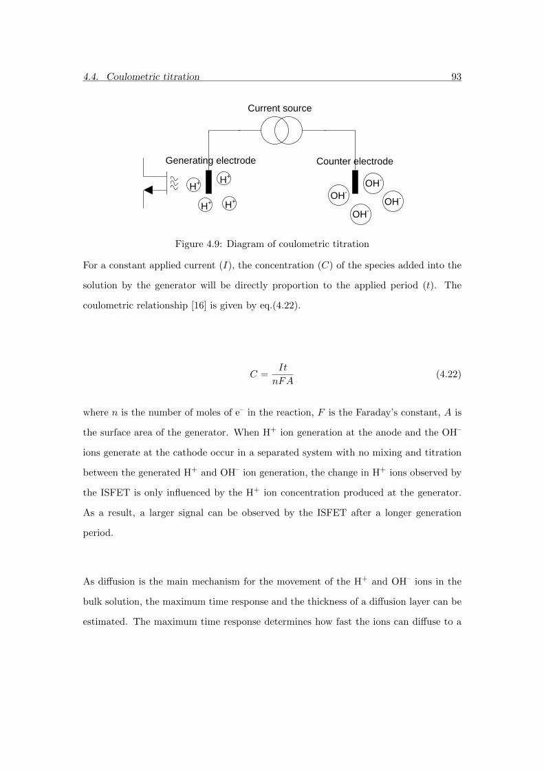
4.4. Coulometric titration 93
Generating electrode Counter electrode
Current source
H+
OH-
OH-
OH-
OH-
H+ H
+
H+
Figure 4.9: Diagram of coulometric titration
For a constant applied current (I), the concentration (C) of the species added into the
solution by the generator will be directly proportion to the applied period (t). The
coulometric relationship [16] is given by eq.(4.22).
C =It
nFA(4.22)
where n is the number of moles of e– in the reaction, F is the Faraday’s constant, A is
the surface area of the generator. When H+ ion generation at the anode and the OH–
ions generate at the cathode occur in a separated system with no mixing and titration
between the generated H+ and OH– ion generation, the change in H+ ions observed by
the ISFET is only influenced by the H+ ion concentration produced at the generator.
As a result, a larger signal can be observed by the ISFET after a longer generation
period.
As diffusion is the main mechanism for the movement of the H+ and OH– ions in the
bulk solution, the maximum time response and the thickness of a diffusion layer can be
estimated. The maximum time response determines how fast the ions can diffuse to a

4.4. Coulometric titration 94
certain distance (i.e. the thickness of a diffusion layer). The relationship between time
and distance of the diffusion phenomena [11] can be described according to the eq.(4.23).
L =√
2Dt (4.23)
where L is the thickness of a diffusion layer, t is time response and D is the diffusion
coefficient. In the case of the hydrogen ions, the diffusion coefficient (DH+) is 9.3×10⁻⁹
m/s2 [33]. If the required minimum response time is assumed as 1ms, the maximum
distance between the generated electrode and the sensor should be less than or equal to
4.31 µm. The significance of this equation is that it can be used as an estimate of the
maximum time response when the distance is known.
Furthermore, other chemical species can also be produced using the coulometric tech-
nique. For instance, Ag+ can be induced by using a silver wire as the generating
electrode, and similarly, by using a mercury wire as the generating electrode, Hg2+ can
be produced.
It should be noted that the coulometric titration technique can only be implemented
where the titrant is in the form of a solid metal. This is because electrical current is
central to this ion generation process. If the interested titrant is not in the rigid form
and has no electrical conductivity, this technique will not be applicable.

4.5. Iontophoresis method 95
4.5 Iontophoresis method
In the case where the titrant is not in the solid form and has no electrical conductivity,
iontophoresis is an alternative approach to create an ion flow in a similar way to the
coulometric titration method. The iontophoresis technique has been extensively used
to conduct experiments in neurological studies especially in the delivery of neuroactive
substances. The diagram of this technique is shown in Fig.(4.10).
Figure 4.10: Diagram of iontophoresis
The ejection of ions in this technique is controlled by the applied current via the current
source. A positive current (i.e. electrode 1 has a positive potential) will repel the posi-
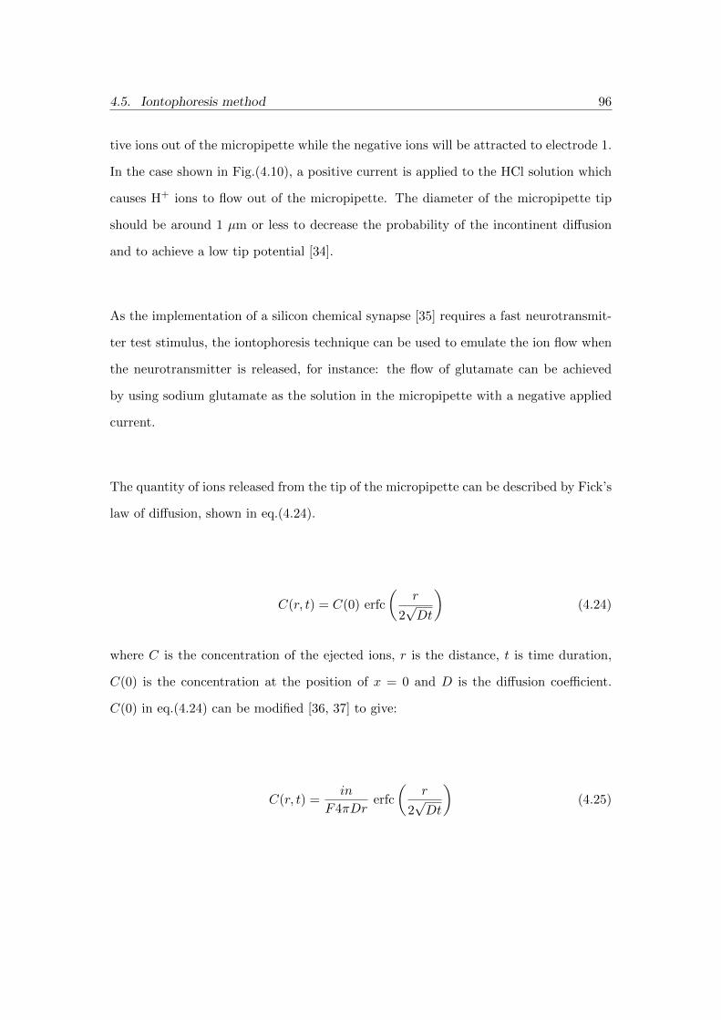
4.5. Iontophoresis method 96
tive ions out of the micropipette while the negative ions will be attracted to electrode 1.
In the case shown in Fig.(4.10), a positive current is applied to the HCl solution which
causes H+ ions to flow out of the micropipette. The diameter of the micropipette tip
should be around 1 µm or less to decrease the probability of the incontinent diffusion
and to achieve a low tip potential [34].
As the implementation of a silicon chemical synapse [35] requires a fast neurotransmit-
ter test stimulus, the iontophoresis technique can be used to emulate the ion flow when
the neurotransmitter is released, for instance: the flow of glutamate can be achieved
by using sodium glutamate as the solution in the micropipette with a negative applied
current.
The quantity of ions released from the tip of the micropipette can be described by Fick’s
law of diffusion, shown in eq.(4.24).
C(r, t) = C(0) erfc
(r
2√Dt
)(4.24)
where C is the concentration of the ejected ions, r is the distance, t is time duration,
C(0) is the concentration at the position of x = 0 and D is the diffusion coefficient.
C(0) in eq.(4.24) can be modified [36, 37] to give:
C(r, t) =in
F4πDrerfc
(r
2√Dt
)(4.25)

4.5. Iontophoresis method 97
where i is an electrical current, F is the Faraday constant and n is the transport num-
bers. To simplify the complement error function (erfc), let’s consider the transformation
of the complement error function shown in eq.(4.26)
erfc(a) =e−a
2
a√π
∞∑n=0
(−1)n · (2n− 1)!!
(2a2)n(4.26)
Substitute a = r2√Dt
into eq.(4.26):
erfc
(r
2√Dt
)=
e−(
r
2√Dt
)2(r
2√Dt
)√π
∞∑n=0
(−1)n · (2n− 1)!!(2(
r2√Dt
)2)n (4.27)
Substitute eq.(4.27) into eq.(4.25):
C(r, t) =in
F4πDr
e−(
r
2√Dt
)2(r
2√Dt
)√π
∞∑n=0
(−1)n · (2n− 1)!!(2(
r2√Dt
)2)n (4.28)
Rearrange eq.(4.28):
C(r, t) =
in2Fr2
√t
Dπ3
exp(r2
4Dt
) ∞∑n=0
(−1)n · (2n− 1)!!(2(
r2√Dt
)2)n (4.29)
Considering only the coefficient terms in eq.(4.29)

4.5. Iontophoresis method 98
C(r, t) ∝in
2Fr2
√t
Dπ3
exp(r2
4Dt
) (4.30)
From the eq.(4.30), it can be observed that the concentration (C) is directly proportional
to the current (i) and time duration (t), while the distance (r) is inversely proportional
to the concentration (C).
Likewise, by only considering eq.(4.25) and neglecting the complementary error func-
tion (erfc), the transport number (n) can be related to the time duration of the injected
current (t). The transport numbers (or transference numbers) of the ion x is defined
as the fraction of the ion x’s conductivity over the whole conductivity [11], shown in
eq.(4.31).
nx =|zx|uxCx∑j
|zj |ujCj(4.31)
where nx is the transport number of the ion x, zx is the magnitude of charge of the
ion x, ux is the mobility of the ion x, and Cx is the concentration of the ion x. From
eq.(4.31), the transport number is directly proportional to the magnitude of the charges.
nx ∝ zx (4.32)
Additionally, the definition of the charges is described as a product of the current (I)
and time (t).
4.6. Experimental results on Iontophoresis 99
zx = It (4.33)
From eq.(4.32) and eq.(4.33), it can be concluded that the transport number is directly
proportional to time.
nx ∝ zx ∝ t (4.34)
The neurotransmitter signal in Destexhe’s chemical synapse model [29] is expressed as a
1ms duration pulse with a 1mM amplitude. To create an ionic perturbation within the
millisecond range, a calculation based on the iontophoresis technique [37] is carried out.
Recalling that the amount of ion concentration ejected at the tip of the micropipette is
given by eq.(4.25). Eq.(4.25) can be re-arranged to give:
i =4FDπr[IONS]
n× erfc( r2√Dt
)(4.35)
Therefore, the required current (i) to generate a 1mM glutamate ([IONS]) change with
a 1ms time duration (t) where the diffusion of glutamate (D) = 2.5×10⁻¹⁰ m2/s [38],
the distance (r) = 2µm, the transport number of glutamate (n) = 0.4 [38] and the
Faraday’s constant (F ) = 96485.3399 C/mol, is 0.4µA.
4.6 Experimental results on Iontophoresis
The system used for the iontophoresis experiment is shown in Fig.(4.11). This system
consists of three main parts: the glass micropipette with 1µm diameter (from World
Precision Instrument Ltd), two platinum electrodes (Pt1 and Pt2), the AC current

4.6. Experimental results on Iontophoresis 100
source (Keithley model 6221), the ISFET from Sentron Europe B.V. and the opamp
driven readout circuit [39]. In the experiment, the 3M HCl solution was put into the
micropipette for H+ perturbation. The bulk solution used in this case was the Phos-
phate Buffer Saline (PBS).
Generating electrode Counter electrode
Current source
OH-
OH-
OH- OH
-
H+ H
+
+
-
HCl solution
Micropipette
H+
Cl-
H+
H+
H+
H+
H+
H+
H+
H+
Cl-
Cl-
Cl-
Cl-
Cl-
Cl-
Cl-
Cl-
Cl-
Cl-
H+
H+
Current source
Electrode1
Electrode2
Chemical Sensor
+
-
HCl solution
Micropipette
H+
Cl-
H+
H+
H+
H+
H+
H+
H+
H+
Cl-
Cl-
Cl-
Cl-
Cl-
Cl-
Cl-
Cl-
Cl-
Cl-
H+
H+
Keithley 6221 AC
Current source
PT1
PT2
Sentron ISFET
G1G2
Reference
electrode
Figure 4.11: System used for iontophoresis experiment
As there was no stirring in this experiment, the convection effect would not influence the
movement of the ejected ions. The change in proton concentration measured through the
ISFET and the readout circuit was a local ion change only; and diffusion was assumed
as the only contribution to the ion concentration fluctuation. The distance between
the ISFET and the tip of micropipette is in order of 1µm; this was controlled by the
micromanipulator. The current source was kept floating to separate the ground of the
current source from the ground of the readout circuit. This floating current source also
ensured that there was no leakage current through the reference electrode.

4.6. Experimental results on Iontophoresis 101
The first part of this experiment was to determine the relationship between the current
amplitude and the concentration change. A current pulse signal with a 1ms pulse width
was used with the amplitude set at -1µA, +0.6µA and +1.0µA. The result from this
experiment is shown in Fig.(4.12).
Figure 4.12: Measured result for three different injected amplitudes at 1µm distancebetween the micropipette tip and the ISFET’s surface (insert is a ’Zoom in’ of oneperiod of the measured result)
It can be observed from the result in Fig.(4.12) that the greater the amplitude of the
current injected (i), the larger the ion concentration (C) sensed by the ISFET, which is
consistent with eq.(4.30). The negative current test at -1µA amplitude, as expected, did
not produce a response. This is correct because the ISFET is only sensitive to changes
in proton or H+ ions and not Cl– ions.

4.6. Experimental results on Iontophoresis 102
A 1µA current signal with three different pulse widths (10ms, 1ms and 0.1ms) were
used as the input signal for the second experiment. The result is shown in Fig.(4.13).
Figure 4.13: Measured result for three different current pulse widths at a fixed injectedamplitude of 1uA and a 1µm distance between the micropipette tip and the ISFET’ssurface (insert is a ’Zoom in’ of one period of the measured result)
It can be seen that the ISFET responded to a 1ms pulse but it could not detect a
0.1ms pulse. With a longer injection time, a larger response was obtained, which agrees
with the eq.(4.30). Satisfactory repeatability of the response was observed in successive
proton injections. From the measured results shown earlier, it can be concluded that
this experiment is the first iontophoresis technique to create and verify a millisecond
H+ perturbation on the ISFET.

4.7. Summary 103
4.7 Summary
This chapter has presented the basic concepts of an ISFET such as its operation, sen-
sitivity, which was explained by chemical theories, and drift, one of its imperfections.
The ISFET’s ability to detect different chemical species by modifying the sensing area,
an ENFET, has been described. Furthermore, the modification procedures to produce
the glutamate ISFET has been given. The non-linear relationship between the concen-
tration of hydrogen ions and the output signal of the traditional voltage-mode readout
circuit [30] have been discussed in this chapter. The required linear relationship between
the ion concentration and the output signal can be achieved with a recent current-mode
readout circuit [31].
The later sections of this chapter examined, in particular, the iontophoresis chemical
perturbation technique for the generation of the neurotransmitter test signal in the
Destexhe’s chemical synapse. From the experimental results of this technique, a one
millisecond signal of [H+] ions could be detected and verified with an ISFET. With the
validity of this technique confirmed, iontophoresis can be employed to simulate a fast
chemical stimulus that is representative of the required neurotransmitter signal [29].

References
[1] B. Palan, K. Roubik, M. Husak, and B. Courtois, “CMOS ISFET-based structures
for biomedical applications,” in Microtechnologies in Medicine and Biology, 1st
Annual International, Conference On. 2000, 2000, pp. 502–506.
[2] P. Bergveld, “Development of an ion-sensitive solid-state device for neurophysiolog-
ical measurements,” Biomedical Engineering, IEEE Transactions on, vol. BME-17,
no. 1, pp. 70–71, 1970.
[3] Y.-Q. Zhang, J. Zhu, and R.-A. Gu, “Improved biosensor for glucose based on
glucose oxidase-immobilized silk fibroin membrane,” Applied Biochemistry and
Biotechnology, vol. 75, pp. 215–233, 1998.
[4] C. Eggenstein, M. Borchardt, C. Diekmann, B. Grndig, C. Dumschat, K. Cam-
mann, M. Knoll, and F. Spener, “A disposable biosensor for urea determination in
blood based on an ammonium-sensitive transducer,” Biosensors and Bioelectronics,
vol. 14, no. 1, pp. 33–41, 1 1999.
[5] Q. Li, S. Zhang, and J. Yu, “Immobilization of l-glutamate oxidase and peroxidase
for glutamate determination in flow injection analysis system,” Applied Biochem-
istry and Biotechnology, vol. 59, pp. 53–61, 1996.
104

REFERENCES 105
[6] H. Kinoshita, M. Torimura, K. Kano, and T. Ikeda, “Peroxidase-based ampero-
metric sensor of hydrogen peroxide generated in oxidase reaction: Application to
creatinine and creatine assay,” Electroanalysis, vol. 9, no. 16, pp. 1234–1238, 1997.
[7] T. Horiuchi, K. Torimitsu, K. Yamamoto, and O. Niwa, “On-line flow sensor for
measuring acetylcholine combined with microdialysis sampling probe,” Electroanal-
ysis, vol. 9, no. 12, pp. 912–916, 1997.
[8] N. Osamu, K. Ryoji, H. Tsutomu, and T. Keiichi, “Small-volume on-line sensor for
continuous measurement of γ-aminobutyric acid,” Analytical Chemistry, vol. 70,
no. 1, pp. 89–93, 1998.
[9] B. Palan, “Design of low noise ph-isfet microsensors and integrated suspended in-
ductors with increased quality factor q,” Ph.D. dissertation, Institut Polytechnique
de Grenoble, 2001.
[10] P. Bergveld, R. E. G. van Hal, and J. C. T. Eijkel, “The remarkable similarity
between the acid-base properties of ISFETs and proteins and the consequences for
the design of isfet biosensors,” Biosensors and Bioelectronics, vol. 10, no. 5, pp.
405–414, 1995.
[11] A. J. Bard and L. R. Faulkner, Electrochemical methods : fundamentals and appli-
cations. New York: Wiley, 2001.
[12] D. E. Yates, S. Levine, and T. W. Healy, “Site-binding model of the electrical double
layer at the oxide/water interface,” J. Chem. Soc., Faraday Trans. 1, vol. 70, pp.
1807–1818, 1974.
[13] L. Shepherd and C. Toumazou, “Weak inversion ISFETs for ultra-low power bio-
chemical sensing and real-time analysis,” Sensors and Actuators B: Chemical, vol.
107, no. 1, pp. 468–473, 5/27 2005.
REFERENCES 106
[14] P. Bergveld, “Thirty years of isfetology: What happened in the past 30 years
and what may happen in the next 30 years,” Sensors and Actuators B: Chemical,
vol. 88, no. 1, pp. 1–20, 1/1 2003.
[15] A. S. Poghossian, “The super-nernstian ph sensitivity of Ta2O5 - gate ISFETs,”
Sensors and Actuators B: Chemical, vol. 7, no. 1-3, pp. 367–370, 3 1992.
[16] B. van der Schoot and P. Bergveld, “An ISFET-based microlitre titrator: integra-
tion of a chemical sensoractuator system,” Sensors and Actuators, vol. 8, no. 1, pp.
11–22, 9 1985.
[17] I.-Y. Huang, R.-S. Huang, and L.-H. Lo, “Improvement of integrated Ag/AgCl thin-
film electrodes by KCl-gel coating for ISFET applications,” Sensors and Actuators
B: Chemical, vol. 94, no. 1, pp. 53–64, 8/15 2003.
[18] P. A. Comte and J. Janata, “A field effect transistor as a solid-state reference
electrode,” Analytica Chimica Acta, vol. 101, no. 2, pp. 247–252, 11/1 1978.
[19] S. Jamasb, S. D. Collins, and R. L. Smith, “Correction of instability in ion-selective
field effect transistors (ISFETs) for accurate continuous monitoring of pH,” in
Engineering in Medicine and Biology Society, 1997. Proceedings of the 19th Annual
International Conference of the IEEE, vol. 5, 1997, pp. 2337–2340 vol.5.
[20] P. A. Hammond and D. R. S. Cumming, “Performance and system-on-chip inte-
gration of an unmodified CMOS ISFET,” Sensors and Actuators B: Chemical, vol.
111-112, pp. 254–258, 11/11 2005.
[21] S. Caras and J. Janata, “Field effect transistor sensitive to penicillin,” Analytical
Chemistry, vol. 52, no. 12, pp. 1935–1937, 1980.
[22] D. G. Pijanowska and W. Torbicz, “pH-ISFET based urea biosensor,” Sensors and
Actuators B: Chemical, vol. 44, no. 1-3, pp. 370–376, 10 1997.
REFERENCES 107
[23] C.-H. Lee, H.-I. Seo, Y.-C. Lee, B.-W. Cho, H. Jeong, and B.-K. Sohn, “All solid
type ISFET glucose sensor with fast response and high sensitivity characteristics,”
Sensors and Actuators B: Chemical, vol. 64, no. 1-3, pp. 37–41, 6/10 2000.
[24] J.-J. Xu, W. Zhao, X.-L. Luo, and H.-Y. Chen, “A sensitive biosensor for lactate
based on layer-by-layer assembling MnO2 nanoparticles and lactate oxidase on ion-
sensitive field-effect transistors,” Chem. Commun., pp. 792–794, 2005.
[25] A. P. Soldatkin, J. Montoriol, W. Sant, C. Martelet, and N. Jaffrezic-Renault, “Cre-
atinine sensitive biosensor based on ISFETs and creatinine deiminase immobilised
in bsa membrane,” Talanta, vol. 58, no. 2, pp. 351–357, 8/23 2002.
[26] D. Braeken, D. R. Rand, A. Andrei, R. Huys, M. E. Spira, S. Yitzchaik, J. Shappir,
G. Borghs, G. Callewaert, and C. Bartic, “Glutamate sensing with enzyme-modified
floating-gate field effect transistors,” Biosensors and Bioelectronics, vol. 24, no. 8,
pp. 2384–2389, 4/15 2009.
[27] A. Yamamura, Y. Kimura, S. Tamai, and K. Matsumoto, “Gamma-aminobutyric
acid (GABA) sensor using GABA oxidase from penicillium sp. kait-m-117,” ECS
Meeting Abstracts, vol. 802, no. 46, pp. 2832–2832, 2008.
[28] A. Hai, D. Ben-Haim, N. Korbakov, A. Cohen, J. Shappir, R. Oren, M. E. Spira,
and S. Yitzchaik, “AcetylcholinesteraseISFET based system for the detection of
acetylcholine and acetylcholinesterase inhibitors,” Biosensors and Bioelectronics,
vol. 22, no. 5, pp. 605–612, 12/15 2006.
[29] Z. F. M. Alain Destexhe and T. J. Sejnowski, Kinetic models of synaptic transmis-
sion., 2nd ed., ser. Methods in Neuronal Modeling (2nd ed.). Cambridge, MA:
MIT Press, 1998, pp. 1–26.

REFERENCES 108
[30] H. Nakajima, M. Esashi, and T. Matsuo, “The pH response of organic gate ISFETs
and the influence of macro-molecule adsorption,” Nippon Kagaku Kaishi, vol. 10,
pp. 1499–1508, 1980.
[31] L. M. Shepherd and C. Toumazou, “A biochemical translinear principle with weak
inversion ISFETs,” Circuits and Systems I: Regular Papers, IEEE Transactions
on, vol. 52, no. 12, pp. 2614–2619, 2005.
[32] B. van der Schoot, P. Bergveld, M. Bos, and L. J. Bousse, “The ISFET in analytical
chemistry,” Sensors and Actuators, vol. 4, pp. 267–272, 1983.
[33] J. C. van Kerkhof, W. Olthuis, P. Bergveld, and M. Bos, “Tungsten trioxide (WO3)
as an actuator electrode material for ISFET-based coulometric sensor-actuator sys-
tems,” Sensors and Actuators B: Chemical, vol. 3, no. 2, pp. 129–138, 2 1991.
[34] U. Windhorst and H. Johansson, Modern techniques in neuroscience research.
Berlin; New York: Springer, 1999.
[35] S. Thanapitak and C. Toumazou, “Towards a bionic chemical synapse,” in Circuits
and Systems, 2009. ISCAS 2009. IEEE International Symposium on, 2009, pp.
677–680.
[36] H. D. Lux and E. Neher, “The equilibration time course of [K+]0 in cat cortex,”
Experimental Brain Research, vol. 17, pp. 190–205, 1973.
[37] E. Neher and H. D. Lux, “Rapid changes of potassium concentration at the outer
surface of exposed single neurons during membrane current flow,” The Journal of
general physiology, vol. 61, no. 3, pp. 385–399, March 01 1973.
[38] A. Herz, W. Zieglgnsberger, and G. Frber, “Microelectrophoretic studies concern-
ing the spread of glutamic acid and GABA in brain tissue,” Experimental brain
research, vol. 9, no. 3, p. 221, 1969.

REFERENCES 109
[39] H. Nakajima, M. Esashi, and T. Matsuo, “The pH-response of organic gate ISFETs
and the influence of macro-molecule adsorption,” J. Chem. Soc. Jpn., vol. 10, pp.
1499–1508, 1980.
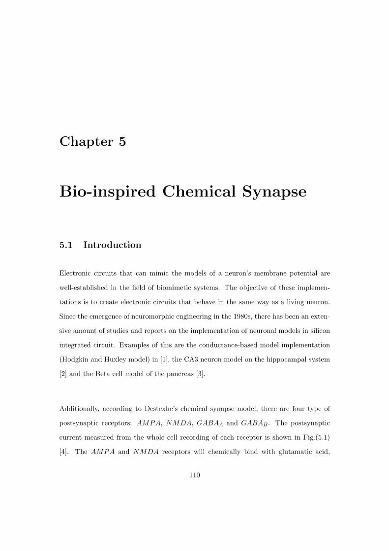
Chapter 5
Bio-inspired Chemical Synapse
5.1 Introduction
Electronic circuits that can mimic the models of a neuron’s membrane potential are
well-established in the field of biomimetic systems. The objective of these implemen-
tations is to create electronic circuits that behave in the same way as a living neuron.
Since the emergence of neuromorphic engineering in the 1980s, there has been an exten-
sive amount of studies and reports on the implementation of neuronal models in silicon
integrated circuit. Examples of this are the conductance-based model implementation
(Hodgkin and Huxley model) in [1], the CA3 neuron model on the hippocampal system
[2] and the Beta cell model of the pancreas [3].
Additionally, according to Destexhe’s chemical synapse model, there are four type of
postsynaptic receptors: AMPA, NMDA, GABAA and GABAB. The postsynaptic
current measured from the whole cell recording of each receptor is shown in Fig.(5.1)
[4]. The AMPA and NMDA receptors will chemically bind with glutamatic acid,
110
5.1. Introduction 111
while γ-aminobutyric acid is the neurotransmitter that can be detected by the GABAA
and GABAB receptors. The profile of the neurotransmitter release from the chem-
ical synapse model of Dextexhe et al. [4] is assumed to be the brief pulse of 1mM
concentration in amplitude and 1ms in duration.Methods in Neuronal Modeling� Chapter � �
100 pA
10 ms
20 pA
200 ms
10 pA
10 ms
AMPA NMDAA B
C D
200 ms
10 pA
GABAA GABAB
Figure ��Best �ts of simpli�ed kinetic models to averaged postsynaptic currents obtained from whole�cell recordings�A� AMPA�kainate�mediated currents� B� NMDA�mediated currents� C� GABAA�mediated currents� D�GABAB�mediated currents� For all graphs� averaged whole�cell recordings of synaptic currents �noisytraces� identical description as in Fig� �� are represented with the best �t obtained using the simplestkinetic models �continuous traces�� Transmitter time course was a pulse of � mM and � ms duration in allcases �A� modi�ed from Destexhe et al�� ��c� C� modi�ed from Destexhe et al�� ��a� D� modi�ed fromDestexhe et al�� ��� �tting procedures described in Appendix B��
Figure 5.1: Postsynaptic current of (A) AMPA receptor, (B) NMDA receptor, (C)GABAA receptor and (D) GABAB receptor [4]
In this thesis, an implementation of the Destexhe’s chemical synapse model will be pre-
sented via a current-mode CMOS integrated circuit that operates in the weak inversion
region. By operating the CMOS integrated circuit in this region, we can both achieve a
low power consumption and the direct arithmetic computation. The main focus of this
work will be the electronic circuit realisation of the four postsynaptic receptor types
in the Destexhe’s chemical synapse: AMPA, NMDA, GABAA and GABAB. The
author sincerely believes that this work will ultimately pave the way for the creation of
5.2. Neural bridge 112
an artificial chemical synapse receptor which has the capability to sense actual neuro-
transmitter releases from the living neurons.
The sensor for the detection of glutamate (i.e. AMPA and NMDA receptors) is the
enzyme-immobilised ISFET with glutamate oxidase. The artificial glutamate stimulus
that represents a neurotransmitter release is established with a micro-tip glass elec-
trode, based on the iontophoresis technique, described in the previous chapter. Due to
the difficulty in accessing the GABA oxidase enzymes to make a γ-aminobutyric acid
ISFET, the GABAA and GABAB silicon synapse receptors will be verified electroni-
cally without a chemical interface.
This chapter will begin by giving two examples of a silicon neuron that has been used
to re-connect a broken neural signal path, which gave rise to the idea of a neural link or
a neural bridge. The following sections will then describe the implementation of each
of the chemical synapse receptors in the Destexhe model [4]. Towards the end of this
chapter, the CMOS implementation of the full postsynaptic circuit that combines the
Hodgkin-Huxley neuron circuit and the bio-inspired chemical synapse will be presented.
5.2 Neural bridge
Since the implementation of an electronic cochlear in the late 1980s [5], bio-inspired
circuits on the CMOS platform, have been employed in many applications. One of the
interesting applications is in neural prosthetic device or neural interfacing. The ultimate
aim of these devices is to replace the damaged or malfunction neurons. This device is
considered as a neural bridge which can be used to re-connect a break in the normal
neural signal path. Two examples of this neural bridge will be shown here.
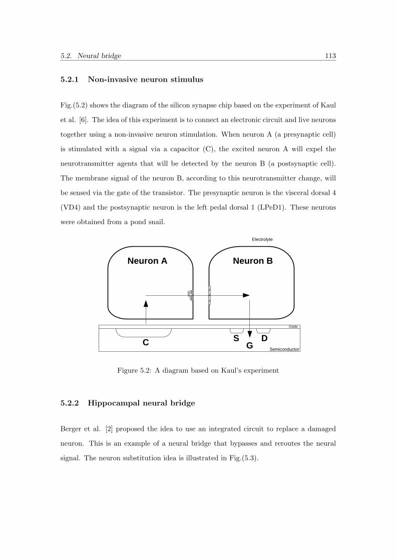
5.2. Neural bridge 113
5.2.1 Non-invasive neuron stimulus
Fig.(5.2) shows the diagram of the silicon synapse chip based on the experiment of Kaul
et al. [6]. The idea of this experiment is to connect an electronic circuit and live neurons
together using a non-invasive neuron stimulation. When neuron A (a presynaptic cell)
is stimulated with a signal via a capacitor (C), the excited neuron A will expel the
neurotransmitter agents that will be detected by the neuron B (a postsynaptic cell).
The membrane signal of the neuron B, according to this neurotransmitter change, will
be sensed via the gate of the transistor. The presynaptic neuron is the visceral dorsal 4
(VD4) and the postsynaptic neuron is the left pedal dorsal 1 (LPeD1). These neurons
were obtained from a pond snail.
C S DG
Oxide
Semiconductor
Electrolyte
Neuron A Neuron B
A B CSensory
input
Mortor
output
A B CSensory
input
Mortor
output
VLSI circuit
Dentate CA1
VLSI circuit
Dentate
CA1
CA3
Figure 5.2: A diagram based on Kaul’s experiment
5.2.2 Hippocampal neural bridge
Berger et al. [2] proposed the idea to use an integrated circuit to replace a damaged
neuron. This is an example of a neural bridge that bypasses and reroutes the neural
signal. The neuron substitution idea is illustrated in Fig.(5.3).

5.2. Neural bridge 114
C S DG
Oxide
Semiconductor
Electrolyte
Neuron A Neuron B
Neuron
A
Sensory
input
Motor
output
Sensory
input
Motor
output
VLSI circuit
Dentate CA1
VLSI circuit
Dentate
CA1
CA3
Neuron
A
Neuron
B
Neuron
C
Neuron
C
Neuron
B
Figure 5.3: A circuit diagram for replacing a dysfunction central brain region with aVLSI system
In this implementation, the central nervous system (CNS) neurons in the hippocampus
region of the brain will be partially replaced by a silicon neuron. Fig.(5.4) shows the
slice view of the hippocampus which is comprised of dentate, CA1 and CA3 subregions.
The flow direction of the neural signal in this area starts from the dentate to CA3 and
CA1 respectively.
C S DG
Oxide
Semiconductor
Electrolyte
Neuron A Neuron B
A B CSensory
input
Mortor
output
A B CSensory
input
Mortor
output
VLSI circuit
Dentate CA1
VLSI circuit
Dentate
CA1
CA3
Figure 5.4: Diagram of the trisynaptic circuit of the hippocampus
In Berger’s work, the physiological properties of the CA3 neuron were modelled math-
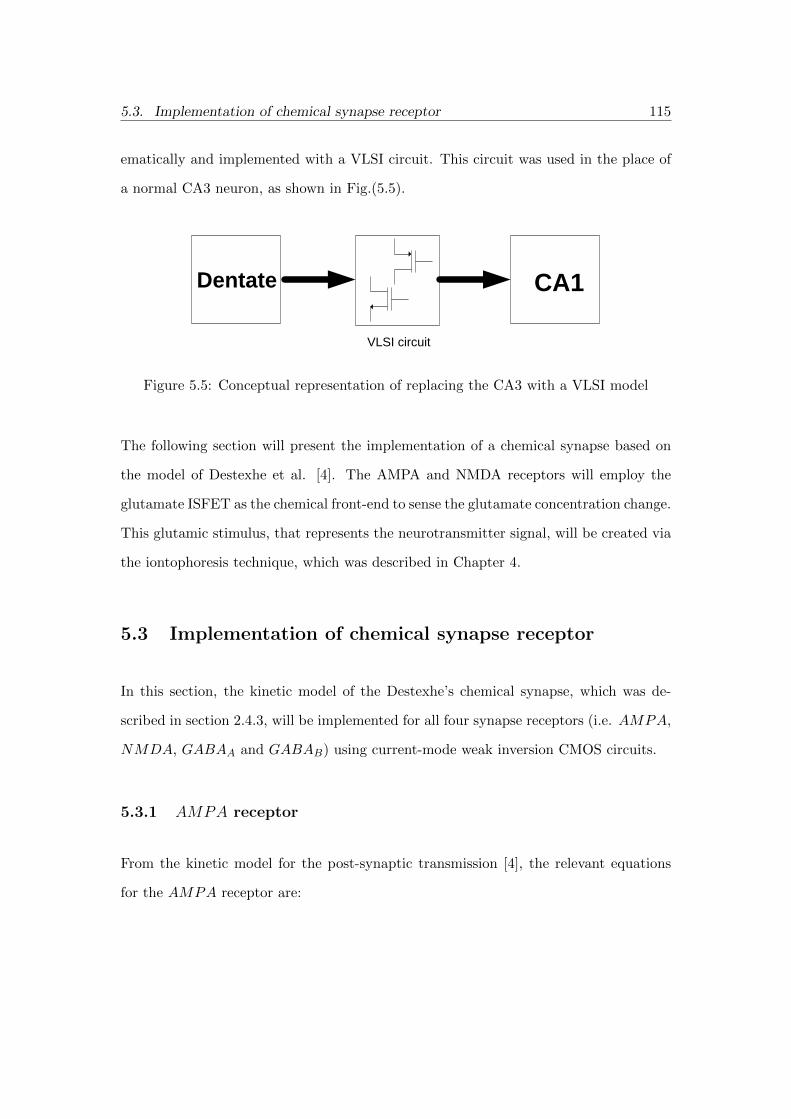
5.3. Implementation of chemical synapse receptor 115
ematically and implemented with a VLSI circuit. This circuit was used in the place of
a normal CA3 neuron, as shown in Fig.(5.5).
C S DG
Oxide
Semiconductor
Electrolyte
Neuron A Neuron B
A B CSensory
input
Mortor
output
A B CSensory
input
Mortor
output
VLSI circuit
Dentate CA1
VLSI circuit
Dentate
CA1
CA3
Figure 5.5: Conceptual representation of replacing the CA3 with a VLSI model
The following section will present the implementation of a chemical synapse based on
the model of Destexhe et al. [4]. The AMPA and NMDA receptors will employ the
glutamate ISFET as the chemical front-end to sense the glutamate concentration change.
This glutamic stimulus, that represents the neurotransmitter signal, will be created via
the iontophoresis technique, which was described in Chapter 4.
5.3 Implementation of chemical synapse receptor
In this section, the kinetic model of the Destexhe’s chemical synapse, which was de-
scribed in section 2.4.3, will be implemented for all four synapse receptors (i.e. AMPA,
NMDA, GABAA and GABAB) using current-mode weak inversion CMOS circuits.
5.3.1 AMPA receptor
From the kinetic model for the post-synaptic transmission [4], the relevant equations
for the AMPA receptor are:
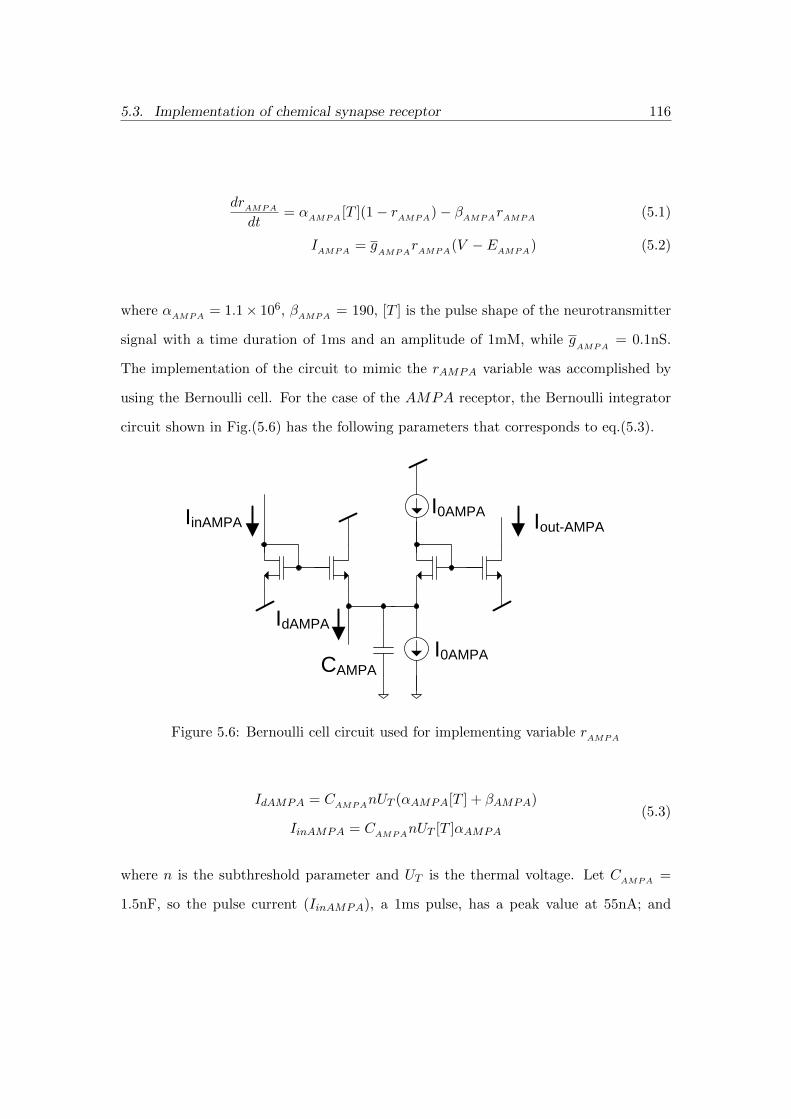
5.3. Implementation of chemical synapse receptor 116
drAMPA
dt= αAMPA [T ](1− rAMPA)− βAMPArAMPA (5.1)
IAMPA = gAMPA
rAMPA(V − EAMPA) (5.2)
where αAMPA = 1.1× 10⁶, βAMPA = 190, [T ] is the pulse shape of the neurotransmitter
signal with a time duration of 1ms and an amplitude of 1mM, while gAMPA
= 0.1nS.
The implementation of the circuit to mimic the rAMPA variable was accomplished by
using the Bernoulli cell. For the case of the AMPA receptor, the Bernoulli integrator
circuit shown in Fig.(5.6) has the following parameters that corresponds to eq.(5.3).
IinAMPA
IdAMPA
CAMPA
Iout-AMPA
I0AMPA
I0AMPA
IinNMDA
IdNMDA
CNMDA
Iout-NMDA
I0NMDA
I0NMDA
Iout-Sig
V1 V2
ISig
ASigASig
IinGABA
IdGABA
CGABA
Iout-GABA
I0GABA
I0GABA
A
A
A
A
A
A
Iin2
Iin2+Id2
C2
I02
I02
IrGABAB
Id3
C3
I0u
I0u
Iout2
Iout3Iin3 Iin3Iin3Iin3
Iin3 Iin3 Iin3Id3 Id3 Id3
Iin4
Id4
Iout4
I04
I04
Figure 5.6: Bernoulli cell circuit used for implementing variable rAMPA
IdAMPA = CAMPAnUT (αAMPA[T ] + βAMPA)
IinAMPA = CAMPAnUT [T ]αAMPA
(5.3)
where n is the subthreshold parameter and UT is the thermal voltage. Let CAMPA =
1.5nF, so the pulse current (IinAMPA), a 1ms pulse, has a peak value at 55nA; and

5.3. Implementation of chemical synapse receptor 117
the DC current, CAMPAnUTβAMPA = 9.5nA. The output current of this Bernoulli cell
(Iout−AMPA) is shown in eq.(5.4).
Iout−AMPA = rAMPAI0AMPA (5.4)
5.3.2 NMDA receptor
For the NMDA receptor, the first order kinetic model and the synaptic current are
given by:
drNMDA
dt= αNMDA [T ](1− rNMDA)− βNMDArNMDA (5.5)
INMDA = gNMDA
B(V )rNMDA(V − ENMDA) (5.6)
where αNMDA = 7.2× 10⁴, βNMDA = 6.6, [T ] is the pulse shape of the neurotransmitter
signal with a time duration of 1ms and an amplitude of 1mM, while gNMDA
= 0.1nS.
For the case of the NMDA receptor, the Bernoulli integrator circuit shown in Fig.(5.7)
has the following parameters that corresponds to eq.(5.7).
IdNMDA = CNMDAnUT (αNMDA[T ] + βNMDA)
IinNMDA = CNMDAnUT [T ]αNMDA
(5.7)
Let CNMDA = 22nF, so the pulse current (IinNMDA), a 1ms pulse, has a peak value at
52.8nA; and the DC current, CNMDAnUTβNMDA = 4.84nA. The output current of this
Bernoulli cell (Iber−NMDA) is shown in eq.(5.8).
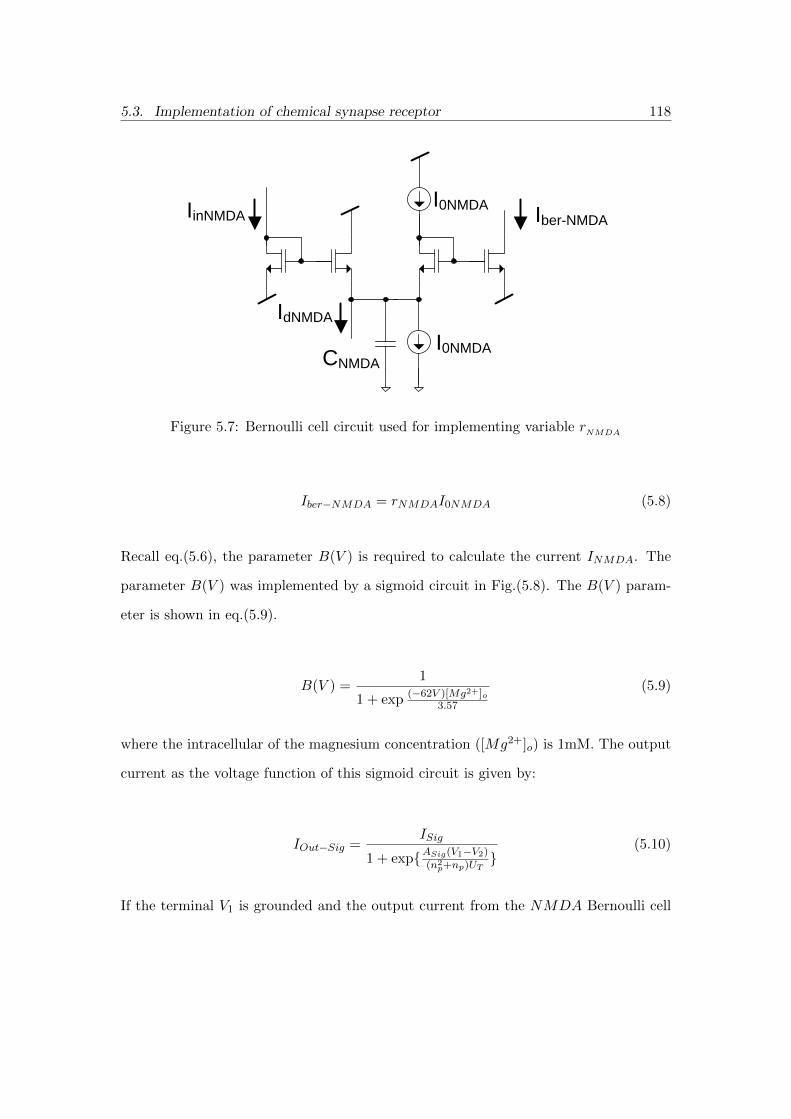
5.3. Implementation of chemical synapse receptor 118
IinAMPA
IdAMPA
CAMPA
Iout-AMPA
I0AMPA
I0AMPA
IinNMDA
IdNMDA
CNMDA
Iber-NMDA
I0NMDA
I0NMDA
Iout-Sig
V1 V2
ISig
ASigASig
IinGABA
IdGABA
CGABA
Iout-GABA
I0GABA
I0GABA
A
A
A
A
A
A
Iin2
Iin2+Id2
C2
I02
I02
IrGABAB
Id3
C3
I0u
I0u
Iout2
Iout3Iin3 Iin3Iin3Iin3
Iin3 Iin3 Iin3Id3 Id3 Id3
Iin4
Id4
Iout4
I04
I04
Figure 5.7: Bernoulli cell circuit used for implementing variable rNMDA
Iber−NMDA = rNMDAI0NMDA (5.8)
Recall eq.(5.6), the parameter B(V ) is required to calculate the current INMDA. The
parameter B(V ) was implemented by a sigmoid circuit in Fig.(5.8). The B(V ) param-
eter is shown in eq.(5.9).
B(V ) =1
1 + exp (−62V )[Mg2+]o3.57
(5.9)
where the intracellular of the magnesium concentration ([Mg2+]o) is 1mM. The output
current as the voltage function of this sigmoid circuit is given by:
IOut−Sig =ISig
1 + exp{ASig(V1−V2)(n2p+np)UT
}(5.10)
If the terminal V1 is grounded and the output current from the NMDA Bernoulli cell

5.3. Implementation of chemical synapse receptor 119
IinAMPA
IdAMPA
CAMPA
Iout-AMPA
I0AMPA
I0AMPA
IinNMDA
IdNMDA
CNMDA
Iout-NMDA
I0NMDA
I0NMDA
Iout-Sig
V1 V2
ISig
ASigASig
IinGABA
IdGABA
CGABA
Iout-GABA
I0GABA
I0GABA
A
A
A
A
A
A
Iin2
Iin2+Id2
C2
I02
I02
IrGABAB
Id3
C3
I0u
I0u
Iout2
Iout3Iin3 Iin3Iin3Iin3
Iin3 Iin3 Iin3Id3 Id3 Id3
Iin4
Id4
Iout4
I04
I04
Figure 5.8: Sigmoid circuit for B(V ) implementation
in Fig.(5.7) is used as the input current for the sigmoid cell (Isig), hence:
IOut−Sig =I0NMDArNMDA
1 + exp { ASig(−V2)(n2p+np)UT
}(5.11)
5.3.3 GABAA receptor
From the kinetic model for post-synaptic transmission [4], the relevant equations for the
GABAA receptor are:
drGABAAdt
= αGABAA [T ](1− rGABAA )− βGABAA rGABAA (5.12)
IGABAA = gGABAA
rGABAA (V − EGABAA) (5.13)
where αGABAA = 5.3 × 10⁵, βGABAA = 180, [T ] is the pulse shape of neurotransmitter

5.3. Implementation of chemical synapse receptor 120
signal with a time duration of 1ms and an amplitude of 1mM and gGABAA
= 0.1nS. The
implementation of the circuit to mimic the rGABAA variable was accomplished by the
Bernoulli cell. For the case of the GABAA receptor, the Bernoulli integrator circuit
shown in Fig.(5.9) has the following parameters that corresponds to eq.(5.14).
IinAMPA
IdAMPA
CAMPA
Iout-AMPA
I0AMPA
I0AMPA
IinNMDA
IdNMDA
CNMDA
Iout-NMDA
I0NMDA
I0NMDA
Iout-Sig
V1 V2
ISig
ASigASig
IinGABA
IdGABA
CGABA
Iout-GABA
I0GABA
I0GABA
A
A
A
A
A
A
Iin2
Iin2+Id2
C2
I02
I02
IrGABAB
Id3
C3
I0u
I0u
Iout2
Iout3Iin3 Iin3Iin3Iin3
Iin3 Iin3 Iin3Id3 Id3 Id3
Iin4
Id4
Iout4
I04
I04
Figure 5.9: Bernoulli cell circuit used for implementing variable rGABAA
IdGABAA = CGABAAnUT (αGABAA [T ] + βGABAA)
IinGABAA = CGABAAnUT [T ]αGABAA
(5.14)
where n is the subthreshold parameter and UT is the thermal voltage. Let CGABAA =
820pF, so the pulse current (IinGABAA), a 1ms pulse, has a peak value at 136.6nA; and
the DC current, CGABAAnUTβGABAA = 4.92nA. The output current of this Bernoulli
cell (Iout−GABAA) is shown in eq.(5.15).
Iout−GABAA = rGABAAI0GABAA (5.15)

5.3. Implementation of chemical synapse receptor 121
5.3.4 GABAB receptor
For the GABAB receptor, the first order kinetic models and the synaptic current are
given by:
drGABABdt
= K1 [T ](1− rGABAB )−K2rGABAB (5.16)
du
dt= K3rGABAB −K4u (5.17)
IGABAB = gGABAB
u4
u4 +Kd(V − EGABAB
) (5.18)
where K1 = 9 × 10⁴M−1s−1, K2 = 1.2s−1, K3 = 180s−1, K4 = 34s−1, n = 4,
Kd = 100µM4, [T ] is the pulse shape of the neurotransmitter signal with a time duration
of 1ms and an amplitude of 1mM and gGABAB
= 0.1nS.
Implementation of the rGABAB and u variables required two Bernoulli cells in cascade as
shown in Fig.(5.10). The first Bernoulli cell creates the variable rGABAB . The relevant
design equations for this variable are:
Id1 = C1nUT (K1[T ] +K2)
Iin1 = C1nUT [T ]K1
IrGABAB = rGABAB I01
(5.19)
Let C1 = 22nF. The pulse current(Iin1) with 1ms pulse width has the maximum current
amplitude at 381nA and the DC current, C1nUTK2 = 1nA. The variable u was generated
by the second Bernoulli cell. The first order differential equation of the second Bernoulli
cell is given by eq.(5.20).
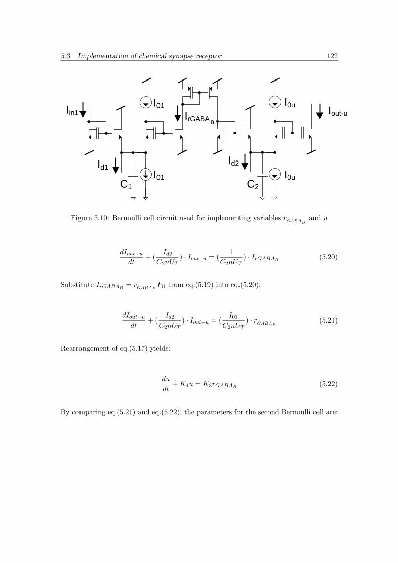
5.3. Implementation of chemical synapse receptor 122
IinAMPA
IdAMPA
CAMPA
Iout-AMPA
I0AMPA
I0AMPA
IinNMDA
IdNMDA
CNMDA
Iber-NMDA
I0NMDA
I0NMDA
Iout-Sig
V1 V2
ISig
ASigASig
IinGABA
IdGABA
CGABA
Iout-GABA
I0GABA
I0GABA
A
A
A
A
A
A
Iin1
Id1
C1
I01
I01
IrGABAB
Id2
C2
I0u
I0u
Iout-u
Iout3Iin3 Iin3Iin3Iin3
Iin3 Iin3 Iin3Id3 Id3 Id3
Iin4
Id4
Iout4
I04
I04
Figure 5.10: Bernoulli cell circuit used for implementing variables rGABAB and u
dIout−udt
+ (Id2
C2nUT) · Iout−u = (
1
C2nUT) · IrGABAB (5.20)
Substitute IrGABAB = rGABAB I01 from eq.(5.19) into eq.(5.20):
dIout−udt
+ (Id2
C2nUT) · Iout−u = (
I01
C2nUT) · rGABAB (5.21)
Rearrangement of eq.(5.17) yields:
du
dt+K4u = K3rGABAB (5.22)
By comparing eq.(5.21) and eq.(5.22), the parameters for the second Bernoulli cell are:
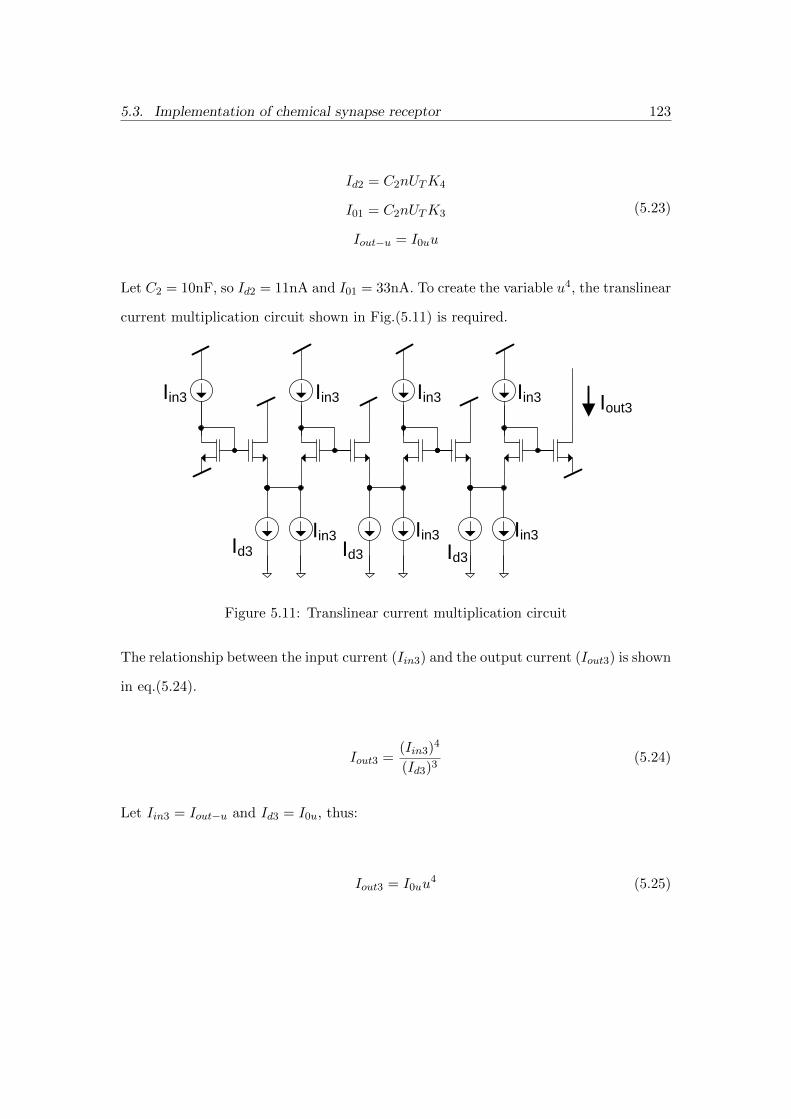
5.3. Implementation of chemical synapse receptor 123
Id2 = C2nUTK4
I01 = C2nUTK3
Iout−u = I0uu
(5.23)
Let C2 = 10nF, so Id2 = 11nA and I01 = 33nA. To create the variable u4, the translinear
current multiplication circuit shown in Fig.(5.11) is required.
IinAMPA
IdAMPA
CAMPA
Iout-AMPA
I0AMPA
I0AMPA
IinNMDA
IdNMDA
CNMDA
Iout-NMDA
I0NMDA
I0NMDA
Iout-Sig
V1 V2
ISig
ASigASig
IinGABA
IdGABA
CGABA
Iout-GABA
I0GABA
I0GABA
A
A
A
A
A
A
Iin2
Iin2+Id2
C2
I02
I02
IrGABAB
Id3
C3
I0u
I0u
Iout2
Iout3Iin3 Iin3Iin3Iin3
Iin3 Iin3 Iin3Id3 Id3 Id3
Iin4
Id4
Iout4
I04
I04
Figure 5.11: Translinear current multiplication circuit
The relationship between the input current (Iin3) and the output current (Iout3) is shown
in eq.(5.24).
Iout3 =(Iin3)4
(Id3)3(5.24)
Let Iin3 = Iout−u and Id3 = I0u, thus:
Iout3 = I0uu4 (5.25)
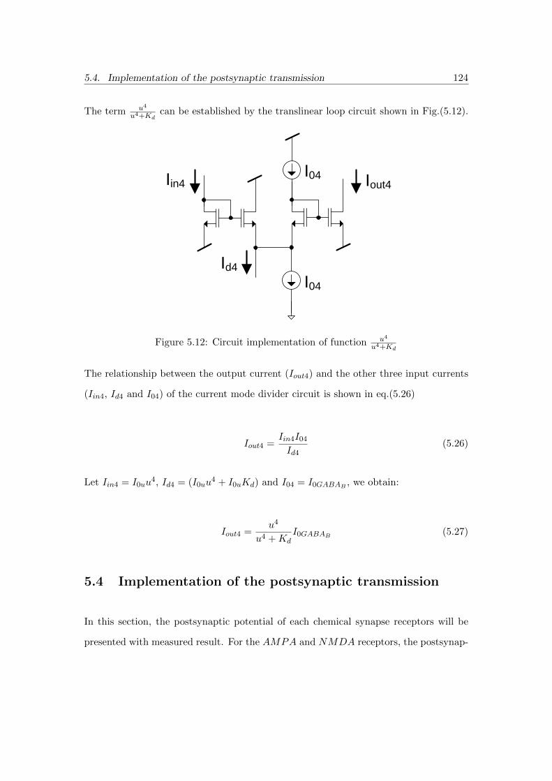
5.4. Implementation of the postsynaptic transmission 124
The term u4
u4+Kdcan be established by the translinear loop circuit shown in Fig.(5.12).
IinAMPA
IdAMPA
CAMPA
Iout-AMPA
I0AMPA
I0AMPA
IinNMDA
IdNMDA
CNMDA
Iout-NMDA
I0NMDA
I0NMDA
Iout-Sig
V1 V2
ISig
ASigASig
IinGABA
IdGABA
CGABA
Iout-GABA
I0GABA
I0GABA
A
A
A
A
A
A
Iin2
Iin2+Id2
C2
I02
I02
IrGABAB
Id3
C3
I0u
I0u
Iout2
Iout3Iin3 Iin3Iin3Iin3
Iin3 Iin3 Iin3Id3 Id3 Id3
Iin4
Id4
Iout4
I04
I04
Figure 5.12: Circuit implementation of function u4
u4+Kd
The relationship between the output current (Iout4) and the other three input currents
(Iin4, Id4 and I04) of the current mode divider circuit is shown in eq.(5.26)
Iout4 =Iin4I04
Id4(5.26)
Let Iin4 = I0uu4, Id4 = (I0uu
4 + I0uKd) and I04 = I0GABAB , we obtain:
Iout4 =u4
u4 +KdI0GABAB (5.27)
5.4 Implementation of the postsynaptic transmission
In this section, the postsynaptic potential of each chemical synapse receptors will be
presented with measured result. For the AMPA and NMDA receptors, the postsynap-
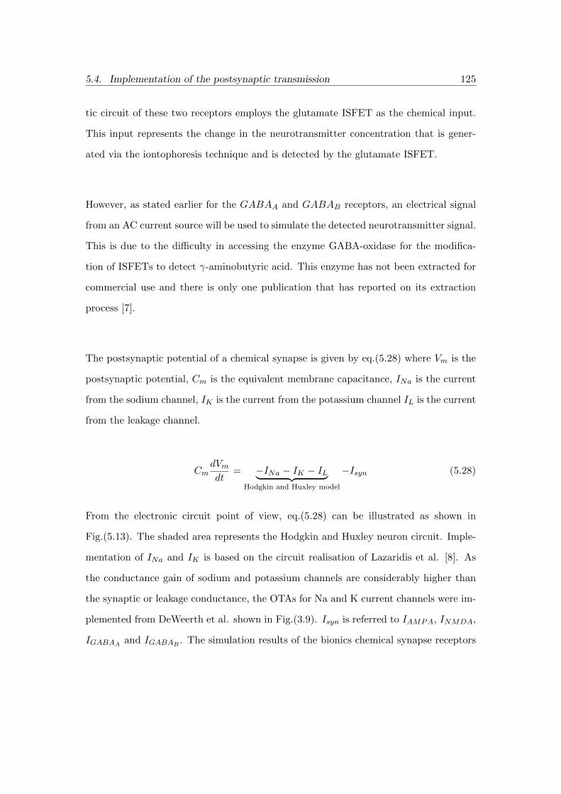
5.4. Implementation of the postsynaptic transmission 125
tic circuit of these two receptors employs the glutamate ISFET as the chemical input.
This input represents the change in the neurotransmitter concentration that is gener-
ated via the iontophoresis technique and is detected by the glutamate ISFET.
However, as stated earlier for the GABAA and GABAB receptors, an electrical signal
from an AC current source will be used to simulate the detected neurotransmitter signal.
This is due to the difficulty in accessing the enzyme GABA-oxidase for the modifica-
tion of ISFETs to detect γ-aminobutyric acid. This enzyme has not been extracted for
commercial use and there is only one publication that has reported on its extraction
process [7].
The postsynaptic potential of a chemical synapse is given by eq.(5.28) where Vm is the
postsynaptic potential, Cm is the equivalent membrane capacitance, INa is the current
from the sodium channel, IK is the current from the potassium channel IL is the current
from the leakage channel.
CmdVmdt
= −INa − IK − IL︸ ︷︷ ︸Hodgkin and Huxley model
−Isyn (5.28)
From the electronic circuit point of view, eq.(5.28) can be illustrated as shown in
Fig.(5.13). The shaded area represents the Hodgkin and Huxley neuron circuit. Imple-
mentation of INa and IK is based on the circuit realisation of Lazaridis et al. [8]. As
the conductance gain of sodium and potassium channels are considerably higher than
the synaptic or leakage conductance, the OTAs for Na and K current channels were im-
plemented from DeWeerth et al. shown in Fig.(3.9). Isyn is referred to IAMPA, INMDA,
IGABAA and IGABAB . The simulation results of the bionics chemical synapse receptors
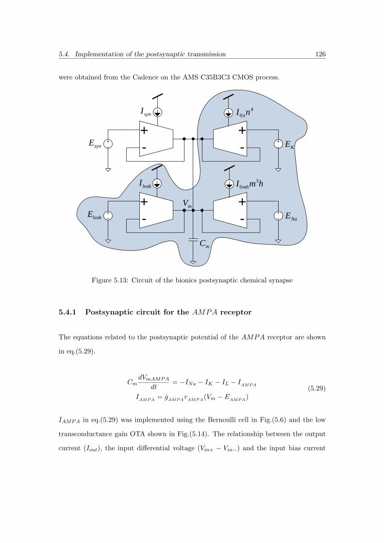
5.4. Implementation of the postsynaptic transmission 126
were obtained from the Cadence on the AMS C35B3C3 CMOS process.
leakI
synI
+-
+-
+-
+-
mC
40 nI n
hmI mh3
0
leakE
synE
NaE
KE
mV
Figure 5.13: Circuit of the bionics postsynaptic chemical synapse
5.4.1 Postsynaptic circuit for the AMPA receptor
The equations related to the postsynaptic potential of the AMPA receptor are shown
in eq.(5.29).
CmdVmAMPA
dt= −INa − IK − IL − IAMPA
IAMPA = gAMPArAMPA(Vm − EAMPA)(5.29)
IAMPA in eq.(5.29) was implemented using the Bernoulli cell in Fig.(5.6) and the low
transconductance gain OTA shown in Fig.(5.14). The relationship between the output
current (Iout), the input differential voltage (Vin+ − Vin−) and the input bias current

5.4. Implementation of the postsynaptic transmission 127
(Ix1) is shown in eq.(5.30). The circuit analysis of this OTA can be viewed in section
3.5.
Iout =(1− 1
np)Ix1(Vin+ − Vin−)
nn(1 + nnnp
+ n2n)(n2
n + nn + 1)16UT(5.30)
where np is the subthreshold slope parameter of PMOS, nn is the subthreshold slope
parameter of NMOS and UT is the thermal voltage.
SigoutI
SigI
1V2VSigASigA
2inI 2outI
02I
2dI
03I
3dI
02I
03I2c3c
applyI
r
+
----
-
++++
Electrode 1
Electrode 2
Micropipette
inVinV
outI
1xI
2xI
6.5
6.5
35.0
100
6.5
2.67
35.0
200
6.5
6.5
6.5
6.5
6.5
6.5
6.5
2.67
35.0
100
35.0
100
35.0
100
35.0
100
35.0
100
35.0
200
35.0
200
35.0
200
35.0
200
35.0
200
35.0
200
35.0
200
6.5
6.5
6.5
6.5
inVinV
outI
1xI
2xI
PBS pH 7
bV
outrI
bI
bI
4
40
4
100
4
40
4
40
4
40
leakI
synI
+
-
+
-
+
-
+
-
mC
4
0 nI n
hmI mh
3
0
leakE
synE
NaE
KE
mV
SigA
1inI 1outI01I
01I11 din II
1C
2inI
02I
02I
3dI
2outIBrGABAI
uI0
uI0
22 din II
2C 3C
3inI3outI3inI
3inI03I
3inI
3inI
03I
3inI
3inI
03I
4inI4outI
04I
4dI
04I
Figure 5.14: Low transconductance gain OTA circuit
The output current (Iout−AMPA) of the Bernoulli cell shown in Fig.(5.6) was designated
as the input bias current of the OTA (Ix1) in Fig.(5.14). In this circuit configuration,

5.4. Implementation of the postsynaptic transmission 128
the output current of the OTA is:
Iout =(1− 1
np)I0AMPA
nn(1 + nnnp
+ n2n)(n2
n + nn + 1)16UT· rAMPA(Vin+ − Vin−) (5.31)
Iout in eq.(5.31) and IAMPA in eq.(5.29) are comparable and it can be concluded that:
gAMPA =(1− 1
np)I0AMPA
nn(1 + nnnp
+ n2n)(n2
n + nn + 1)16UT(5.32)
From the biological model of the AMPA receptor, the conductance gain of AMPA
(gAMPA) is 0.1nS [4]. Thus, I0AMPA can be calculated based on this expression.
I0AMPA =gAMPAnn(1 + nn
np+ n2
n)(n2n + nn + 1)16UT
(1− 1np
)(5.33)
With nn = 1.3, np = 1.28 and UT=25.82mV @ 300K, I0AMPA is 3.6nA. The amplitude
of IdAMPA based on CAMPA = 1.5nF is 9.5nA.
The glutamate ISFET or the neurotransmitter sensor of this receptor couples the glu-
tamate concentration change via the current-mode ISFET readout circuit of Shep-
herd et al. [9]. The output current of this readout circuit represents IinAMPA or
CAMPAnUT [T ]αAMPA in eq.(5.14).
CAMPAnUT [T ]αAMPA = Ibe2γnUT e
−2VbAMPAnUT [ions] (5.34)
Rearranging eq.(5.34) yields:
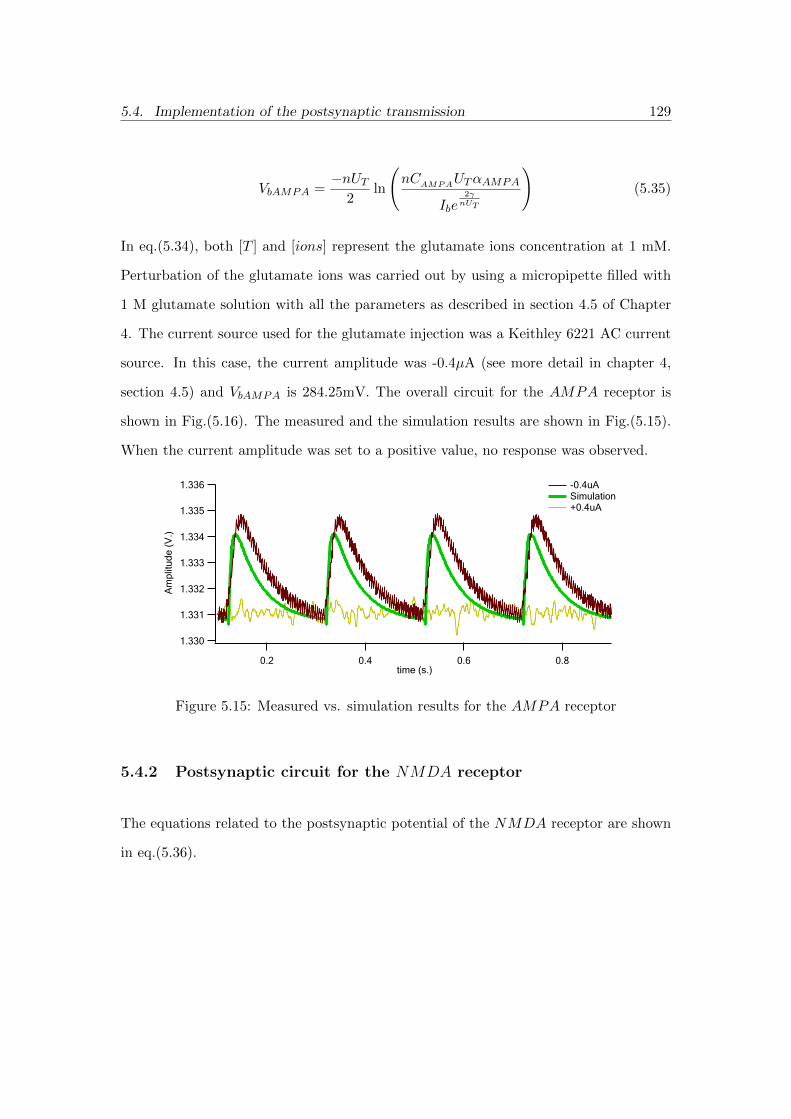
5.4. Implementation of the postsynaptic transmission 129
VbAMPA =−nUT
2ln
(nCAMPAUTαAMPA
Ibe2γnUT
)(5.35)
In eq.(5.34), both [T ] and [ions] represent the glutamate ions concentration at 1 mM.
Perturbation of the glutamate ions was carried out by using a micropipette filled with
1 M glutamate solution with all the parameters as described in section 4.5 of Chapter
4. The current source used for the glutamate injection was a Keithley 6221 AC current
source. In this case, the current amplitude was -0.4µA (see more detail in chapter 4,
section 4.5) and VbAMPA is 284.25mV. The overall circuit for the AMPA receptor is
shown in Fig.(5.16). The measured and the simulation results are shown in Fig.(5.15).
When the current amplitude was set to a positive value, no response was observed.
�����
�����
�����
�����
�����
�����
�����
�� ��������
������������� � ����
������ ���� �������
Figure 5.15: Measured vs. simulation results for the AMPA receptor
5.4.2 Postsynaptic circuit for the NMDA receptor
The equations related to the postsynaptic potential of the NMDA receptor are shown
in eq.(5.36).
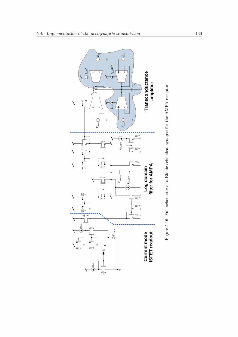
5.4. Implementation of the postsynaptic transmission 130
leak
I
+ - + -
+ - + -
mC
4
0n
In
hm
Im
h
3
0
leak
EN
aE
KE
AM
PA
E
440
4
100
440
440
440
50
nA
50
nA
310
310
310
310
310
35
35
35
310
310
bA
MP
AV
AM
PA
dI1
AM
PA
C1
AM
PA
I 01
mA
MP
AV
310
310
310
35
310
310
leak
I
+ - + -
+ - + -
mC
4
0n
In
hm
Im
h
3
0
leak
EN
aE
KE
440
4
100
440
440
440
50
nA
50
nA
NM
DA
E
310
310
mN
MD
AV
Sig
A
mN
MD
AV
310
310
310
310
310
310
310
310
310
310
310
310
35
35
35
35310
310
310
310
310
310
bN
MD
AV
NM
DA
dI1
NM
DA
C1
NM
DA
I 01
leak
I
+ - + -
+ - + -
mC
4
0n
In
hm
Im
h
3
0
leak
EN
aE
KE
310
310
310
310
310
35
35
35
310
310
AG
AB
AdI
1
AG
AB
AC
1A
GA
BA
I 01
310
310
310
35
310
310
AG
AB
AE
Am
GA
BA
V
Ain
GA
BA
I
Cu
rre
nt
mo
de
ISF
ET
re
ad
ou
t
Lo
g d
om
ain
filt
er
for
AM
PA
Tra
ns
co
nd
uc
tan
ce
am
plifi
er
Cu
rre
nt
mo
de
ISF
ET
re
ad
ou
tL
og
do
ma
in
filt
er
for
NM
DA
Tra
ns
co
nd
uc
tan
ce
am
plifi
er
Lo
g d
om
ain
filt
er
for
GA
BA
A
Tra
ns
co
nd
uc
tan
ce
am
plifi
er
02
I
2C
3dI
2out
IB
rGA
BA
I
uI 0
3C
03
I
04
I
leak
I
+ - + -
+ - + -
mC
4
0n
In
hm
Im
h
3
0
leak
EN
aE
KE
BG
AB
AE
Bm
GA
BA
V
310
310
310
310
310
310
310
310
310
2dI
35
35
35
35
35
310
310
310
35
310
310
35
35
310
310
310
310
310
310
310
310
310
310
310
310
35
35
35
35
35
35
35
35
310
310
310
310
310
310
310
310
35
35
35
35
310
310
310
310
310
310
310
310
310
310
310
udI
K0
Bin
GA
BA
I
Sig
mo
id c
irc
uit
fo
r
B(V
)
Tra
ns
co
nd
uc
tan
ce
am
plifi
er
Cu
rre
nt
mo
de
div
ide
r c
irc
uit
Cu
rre
nt
mo
de
4th
po
we
r c
irc
uit
Lo
g d
om
ain
filt
er
for
GA
BA
B
Fig
ure
5.16
:F
ull
sch
emat
icof
aB
ion
ics
chem
ical
syn
apse
for
the
AM
PA
rece
pto
r
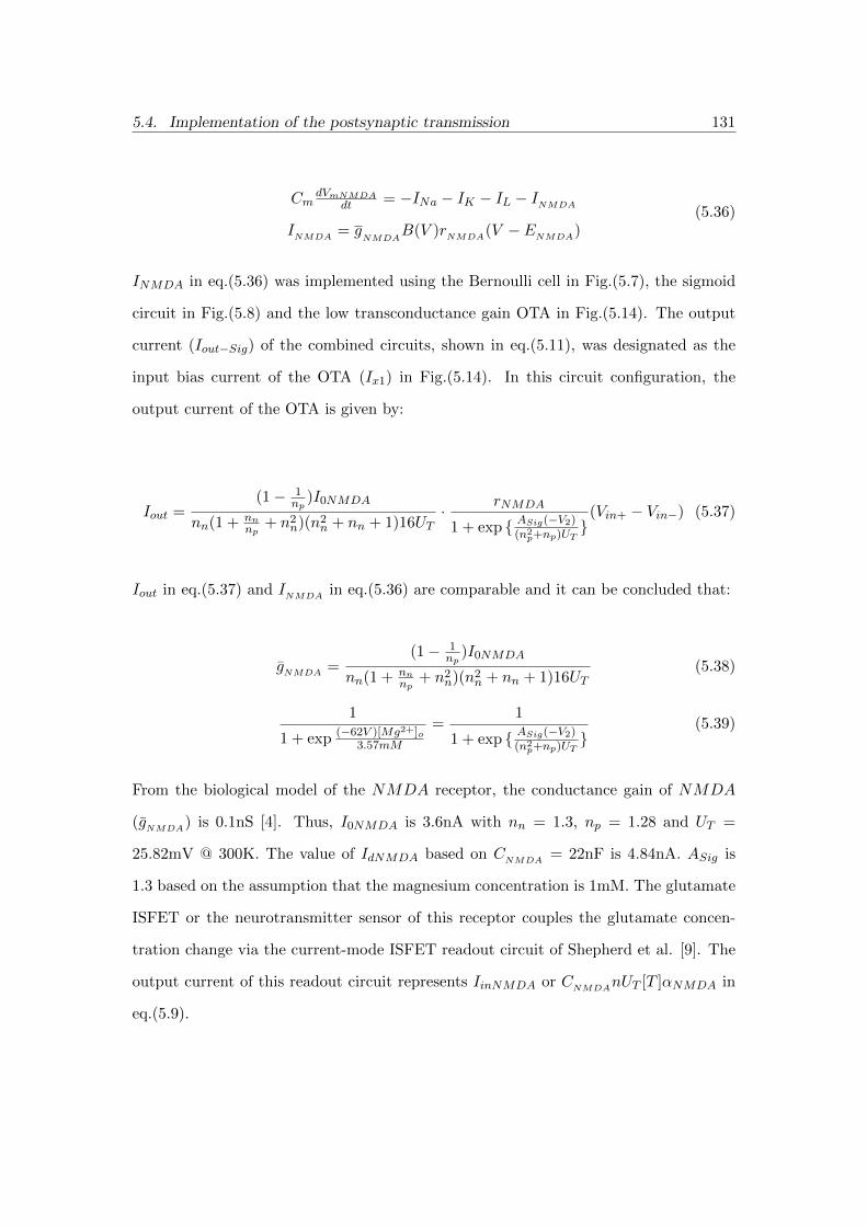
5.4. Implementation of the postsynaptic transmission 131
CmdVmNMDA
dt = −INa − IK − IL − INMDA
INMDA = gNMDA
B(V )rNMDA(V − ENMDA)(5.36)
INMDA in eq.(5.36) was implemented using the Bernoulli cell in Fig.(5.7), the sigmoid
circuit in Fig.(5.8) and the low transconductance gain OTA in Fig.(5.14). The output
current (Iout−Sig) of the combined circuits, shown in eq.(5.11), was designated as the
input bias current of the OTA (Ix1) in Fig.(5.14). In this circuit configuration, the
output current of the OTA is given by:
Iout =(1− 1
np)I0NMDA
nn(1 + nnnp
+ n2n)(n2
n + nn + 1)16UT· rNMDA
1 + exp { ASig(−V2)(n2p+np)UT
}(Vin+ − Vin−) (5.37)
Iout in eq.(5.37) and INMDA in eq.(5.36) are comparable and it can be concluded that:
gNMDA =(1− 1
np)I0NMDA
nn(1 + nnnp
+ n2n)(n2
n + nn + 1)16UT(5.38)
1
1 + exp (−62V )[Mg2+]o3.57mM
=1
1 + exp { ASig(−V2)(n2p+np)UT
}(5.39)
From the biological model of the NMDA receptor, the conductance gain of NMDA
(gNMDA) is 0.1nS [4]. Thus, I0NMDA is 3.6nA with nn = 1.3, np = 1.28 and UT =
25.82mV @ 300K. The value of IdNMDA based on CNMDA = 22nF is 4.84nA. ASig is
1.3 based on the assumption that the magnesium concentration is 1mM. The glutamate
ISFET or the neurotransmitter sensor of this receptor couples the glutamate concen-
tration change via the current-mode ISFET readout circuit of Shepherd et al. [9]. The
output current of this readout circuit represents IinNMDA or CNMDAnUT [T ]αNMDA in
eq.(5.9).

5.4. Implementation of the postsynaptic transmission 132
CNMDAnUT [T ]αNMDA = Ibe2γnUT e
−2VbNMDAnUT [ions] (5.40)
Rearranging eq.(5.40) yields:
VbNMDA =−nUT
2ln
(nCNMDAUTαNMDA
Ibe2γnUT
)(5.41)
In eq.(5.40), [T ] and [ions] both represent the glutamate ions concentration at 1 mM.
Perturbation of the glutamate ions was carried out by using a micropipette filled with
1 M glutamate solution with all the parameters as described in section 4.5 of Chapter
4. The current source used for the glutamate injection was a Keithley 6221 AC current
source. In this case, the current amplitude was -0.4µA and VbNMDA was 284.92mV.
The overall circuit for the NMDA receptor is shown in Fig.(5.18). The measured and
circuit simulation results are shown in Fig.(5.17). When the current amplitude was set
to a positive value, no response was observed.
������
������
������
������
������
�� ��������
������ � ����
������ ���� �������
Figure 5.17: Measured vs. simulation results for the NMDA receptor

5.4. Implementation of the postsynaptic transmission 133le
ak
I
+ - + -
+ - + -
mC
4
0n
In
hm
Im
h
3
0
leak
EN
aE
KE
AM
PA
E
440
4
100
440
440
440
50
nA
50
nA
310
310
310
310
310
35
35
35
310
310
bA
MP
AV
AM
PA
dI1
AM
PA
C1
AM
PA
I 01
mA
MP
AV
310
310
310
35
310
310
leak
I
+ - + -
+ - + -
mC
4
0n
In
hm
Im
h
3
0
leak
EN
aE
KE
440
4
100
440
440
440
50
nA
50
nA
NM
DA
E
310
310
mN
MD
AV
Sig
A
mN
MD
AV
310
310
310
310
310
310
310
310
310
310
310
310
35
35
35
35310
310
310
310
310
310
bN
MD
AV
NM
DA
dI1
NM
DA
C1
NM
DA
I 01
leak
I
+ - + -
+ - + -
mC
4
0n
In
hm
Im
h
3
0
leak
EN
aE
KE
310
310
310
310
310
35
35
35
310
310
AG
AB
AdI
1
AG
AB
AC
1A
GA
BA
I 01
310
310
310
35
310
310
AG
AB
AE
Am
GA
BA
V
Ain
GA
BA
I
Cu
rre
nt
mo
de
ISF
ET
re
ad
ou
t
Lo
g d
om
ain
filt
er
for
AM
PA
Tra
ns
co
nd
uc
tan
ce
am
plifi
er
Cu
rre
nt
mo
de
ISF
ET
re
ad
ou
tL
og
do
ma
in
filt
er
for
NM
DA
Tra
ns
co
nd
uc
tan
ce
am
plifi
er
Lo
g d
om
ain
filt
er
for
GA
BA
A
Tra
ns
co
nd
uc
tan
ce
am
plifi
er
02
I
2C
3dI
2out
IB
rGA
BA
I
uI 0
3C
03
I
04
I
leak
I
+ - + -
+ - + -
mC
4
0n
In
hm
Im
h
3
0
leak
EN
aE
KE
BG
AB
AE
Bm
GA
BA
V
310
310
310
310
310
310
310
310
310
2dI
35
35
35
35
35
310
310
310
35
310
310
35
35
310
310
310
310
310
310
310
310
310
310
310
310
35
35
35
35
35
35
35
35
310
310
310
310
310
310
310
310
35
35
35
35
310
310
310
310
310
310
310
310
310
310
310
udI
K0
Bin
GA
BA
I
Sig
mo
id c
irc
uit
fo
r
B(V
)
Tra
ns
co
nd
uc
tan
ce
am
plifi
er
Cu
rre
nt
mo
de
div
ide
r c
irc
uit
Cu
rre
nt
mo
de
4th
po
we
r c
irc
uit
Lo
g d
om
ain
filt
er
for
GA
BA
B
Fig
ure
5.1
8:
Fu
llsc
hem
atic
ofa
Bio
nic
sch
emic
alsy
nap
sefo
rth
eN
MD
Are
cep
tor

5.4. Implementation of the postsynaptic transmission 134
5.4.3 Postsynaptic circuit for the GABAA receptor
The equations related to the postsynaptic potential of the GABAA receptor are shown
in eq.(5.42).
CmdVmGABAA
dt= −INa − IK − IL − IGABAA
IGABAA = gGABAA rGABAA (Vm − EGABAA)
(5.42)
IGABAA in eq.(5.42) was implemented using the Bernoulli cell in Fig.(5.8) and the low
transconductance gain OTA in Fig.(5.14). The relationship between the output current
(Iout), the input differential voltage (Vin+ − Vin−) and the input bias current (Ix1) is
shown in eq.(5.30).
The output current (Iout−GABAA) of the Bernoulli cell shown in Fig.(5.8) was designated
as the input bias current of the OTA (Ix1) in Fig.(5.14). In this circuit configuration,
the output current of the OTA is:
Iout =(1− 1
np)I0GABAA
nn(1 + nnnp
+ n2n)(n2
n + nn + 1)16UT· rGABAA(Vin+ − Vin−) (5.43)
Iout in eq.(5.43) and IGABAA in eq.(5.42) are comparable and it can be concluded that:
gGABAA =(1− 1
np)I0GABAA
nn(1 + nnnp
+ n2n)(n2
n + nn + 1)16UT(5.44)
From the biological model of the GABAA receptor, the conductance gain of GABAA
(gGABAA ) is 0.1nS [4]. Thus, I0GABAA can be calculated based on this expression:

5.4. Implementation of the postsynaptic transmission 135
I0GABAA =gGABAAnn(1 + nn
np+ n2
n)(n2n + nn + 1)16UT
(1− 1np
)(5.45)
With nn = 1.3, np = 1.28 and UT = 25.82mV @ 300K, I01GABAA is 3.6nA. The value of
Id1GABAA based on C1GABAA = 820pF is 4.92nA, while the input pulse current IinGABAA
has the maximum peak at 136.6nA. Fig.(5.20) shows the overall circuit of the GABAA
receptor. The measured and simulation results are shown in Fig.(5.19).
�����
�����
�����
�����
�����
���� ������
���������������������� ����
���� ������ �����
Figure 5.19: Measured vs. simulation results for the GABAA receptor

5.4. Implementation of the postsynaptic transmission 136
leakI
+
-
+
-
+
-
+
-
mC
4
0 nI n
hmI mh
3
0
leakENaE
KEAMPAE
4
40
4
100
4
40
4
40
4
40
50 nA
50 nA
3
10
3
10
3
10
3
10
3
10
3
5
3
5
3
5
3
10
3
10
bAMPAV
AMPAdI 1
AMPAC1 AMPAI01
mAMPAV
3
10
3
10
3
10
3
5
3
10
3
10
leakI
+
-
+
-
+
-
+
-
mC
4
0 nI n
hmI mh
3
0
leakENaE
KE4
40
4
100
4
40
4
40
4
40
50 nA
50 nA
NMDAE
3
10
3
10
mNMDAV
SigA
mNMDAV
3
10
3
10
3
10
3
103
10
3
10
3
10
3
10
3
10
3
10
3
10
3
10
3
5
3
5
3
5
3
53
10
3
10
3
10
3
10
3
10
3
10
bNMDAV
NMDAdI 1
NMDAC1
NMDAI01
leakI
+
-
+
-
+
-
+
-
mC
4
0 nI n
hmI mh
3
0
leakENaE
KE
3
10
3
10
3
10
3
10
3
10
3
5
3
5
3
5
3
10
3
10
AGABAdI 1
AGABAC1AGABAI01
3
10
3
10
3
10
3
5
3
10
3
10
AGABAE
AmGABAV
AinGABAI
Current mode
ISFET readout
Log domain
filter for AMPATransconductance
amplifier
Current mode
ISFET readoutLog domain
filter for NMDA
Transconductance
amplifier
Log domain
filter for GABAA
Transconductance
amplifier
02I
2C3dI
2outIBrGABAI
uI0
3C
03I
04I
leakI
+
-
+
-
+
-
+
-
mC
4
0 nI n
hmI mh
3
0
leakENaE
KEBGABAE
BmGABAV
3
10
3
10
3
10
3
10
3
10
3
10
3
10
3
10
3
10
2dI
3
5
3
5
3
5
3
5
3
5
3
10
3
10
3
10
3
5
3
10
3
10
3
5
3
5
3
10
3
10
3
10
3
10
3
10
3
10
3
10
3
10 3
10
3
10
3
10
3
10
3
5
3
5
3
5
3
5
3
5
3
5
3
5
3
5
3
10
3
10
3
10
3
10
3
10
3
10
3
10
3
10
3
5
3
5
3
5
3
5
3
10
3
10
3
10
3
10
3
10
3
10
3
10
3
103
10
3
10
3
10
udIK 0
BinGABAI
Sigmoid circuit for
B(V)
Transconductance
amplifier
Current mode
divider circuit
Current
mode 4th
power circuitLog domain
filter for GABAB
Figure 5.20: Full schematic of a Bionics chemical synapse for the GABAA receptor
5.4.4 Postsynaptic circuit for the GABAB receptor
The equations related to the postsynaptic potential of the GABAA receptor are shown
in eq.(5.46).
CmdVmGABAB
dt= −INa − IK − IL − IGABAB
IGABAB = gGABAB
u4
u4 +Kd(V − EGABAB
)(5.46)
IGABAB in eq.(5.46) was implemented using the Bernoulli cell in Fig.(5.10), the current
multiplication circuit in Fig.(5.11), the current divider circuit in Fig.(5.12) and the low
transconductance gain OTA in Fig.(5.14). The relationship between the output current
(Iout), the input differential voltage (Vin+ − Vin−) and the input bias current (Ix1) is
shown in eq.(5.30).

5.4. Implementation of the postsynaptic transmission 137
The output current (Iout4) of the circuit that implements u4
u4+Kdshown in Fig.(5.12)
was designated as the input bias current of the OTA (Ix1) in Fig.(5.14). In this circuit
configuration, the output current of the OTA is given by:
Iout =(1− 1
np)I0GABAB
nn(1 + nnnp
+ n2n)(n2
n + nn + 1)16UT· u4
u4 +Kd(Vin+ − Vin−) (5.47)
Iout in eq.(5.47) and IGABAB in eq.(5.46) was comparable and it can be concluded that:
gGABAB =(1− 1
np)I0GABAB
nn(1 + nnnp
+ n2n)(n2
n + nn + 1)16UT(5.48)
From the biological model of the GABAB receptor, the conductance gain of GABAB
(gGABAB ) is 0.1nS [4]. Thus, I0GABAB can be calculated based on this expression:
I0GABAB =gGABABnn(1 + nn
np+ n2
n)(n2n + nn + 1)16UT
(1− 1np
)(5.49)
With nn = 1.3, np = 1.28 and UT = 25.82mV @ 300K, I0GABAB is 3.6nA. Based on C1
= 22nF, C2 = 10nF, Id1 = 1nA, Id2 = 11nA, I01 = 33nA, I0u = 10nA and I0uKd = 1nA,
while the input pulse current IinGABAB has the maximum peak at 381nA. Fig.(5.22)
shows the overall circuit of the GABAB receptor. The measured and simulation results
are shown in Fig.(5.21).
A microphotograph of the fabricated chemical synapse integrated circuit is shown in
Fig.(5.23). The chip area of the four chemical synapses is 1120 × 1120 µm2. The total
power dissipation of all the circuits in this chip is 168.3µW from a 3.3V supply. The
printed circuit board used in this thesis was designed in Orcad version 15.1. Dimension
of this board is 350mm x 350mm. A photograph of this PCB is shown in Fig.(5.24).

5.4. Implementation of the postsynaptic transmission 138
������
������
������
������
������
�����
�����
�� ���������
��������� ����
���� �������������
Figure 5.21: Measured vs. simulation results for the GABAB receptor
The overall experimental setup is shown in Fig.(5.25). The closed up illustration of the
tip of the micropipette and the glutamate ISFET is shown in Fig.(5.26).
Figure 5.23: Microphotograph of the fabricated chemical synapse

5.4. Implementation of the postsynaptic transmission 139
leak
I
+ - + -
+ - + -
mC
4
0n
In
hm
Im
h
3
0
leak
EN
aE
KE
AM
PA
E
440
4
100
440
440
440
50
nA
50
nA
310
310
310
310
310
35
35
35
310
310
bA
MP
AV
AM
PA
dI1
AM
PA
C1
AM
PA
I 01
mA
MP
AV
310
310
310
35
310
310
leak
I
+ - + -
+ - + -
mC
4
0n
In
hm
Im
h
3
0
leak
EN
aE
KE
440
4
100
440
440
440
50
nA
50
nA
NM
DA
E
310
310
mN
MD
AV
Sig
A
mN
MD
AV
310
310
310
310
310
310
310
310
310
310
310
310
35
35
35
35310
310
310
310
310
310
bN
MD
AV
NM
DA
dI1
NM
DA
C1
NM
DA
I 01
leak
I
+ - + -
+ - + -
mC
4
0n
In
hm
Im
h
3
0
leak
EN
aE
KE
310
310
310
310
310
35
35
35
310
310
AG
AB
AdI
1
AG
AB
AC
1A
GA
BA
I 01
310
310
310
35
310
310
AG
AB
AE
Am
GA
BA
V
Ain
GA
BA
I
Cu
rre
nt
mo
de
ISF
ET
re
ad
ou
t
Lo
g d
om
ain
filt
er
for
AM
PA
Tra
ns
co
nd
uc
tan
ce
am
plifi
er
Cu
rre
nt
mo
de
ISF
ET
re
ad
ou
tL
og
do
ma
in
filt
er
for
NM
DA
Tra
ns
co
nd
uc
tan
ce
am
plifi
er
Lo
g d
om
ain
filt
er
for
GA
BA
A
Tra
ns
co
nd
uc
tan
ce
am
plifi
er
02
I
2C
3dI
2out
IB
rGA
BA
I
uI 0
3C
03
I
04
I
leak
I
+ - + -
+ - + -
mC
4
0n
In
hm
Im
h
3
0
leak
EN
aE
KE
BG
AB
AE
Bm
GA
BA
V
310
310
310
310
310
310
310
310
310
2dI
35
35
35
35
35
310
310
310
35
310
310
35
35
310
310
310
310
310
310
310
310
310
310
310
310
35
35
35
35
35
35
35
35
310
310
310
310
310
310
310
310
35
35
35
35
310
310
310
310
310
310
310
310
310
310
310
udI
K0
Bin
GA
BA
I
Sig
mo
id c
irc
uit
fo
r
B(V
)
Tra
ns
co
nd
uc
tan
ce
am
plifi
er
Cu
rre
nt
mo
de
div
ide
r c
irc
uit
Cu
rre
nt
mo
de
4th
po
we
r c
irc
uit
Lo
g d
om
ain
filt
er
for
GA
BA
B
Fig
ure
5.2
2:
Fu
llsc
hem
atic
ofa
Bio
nic
sch
emic
alsy
nap
sefo
rth
eGABAB
rece
pto
r
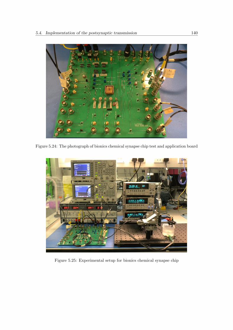
5.4. Implementation of the postsynaptic transmission 140
Figure 5.24: The photograph of bionics chemical synapse chip test and application board
Figure 5.25: Experimental setup for bionics chemical synapse chip
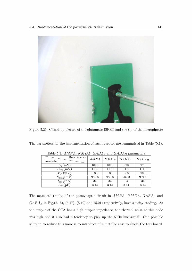
5.4. Implementation of the postsynaptic transmission 141
Figure 5.26: Closed up picture of the glutamate ISFET and the tip of the micropipette
The parameters for the implementation of each receptor are summarised in Table (5.1).
Table 5.1: AMPA, NMDA, GABAA and GABAB parametershhhhhhhhhhhhhhhParameter
Receptor(x)AMPA NMDA GABAA GABAB
Ex(mV) 1070 1070 970 970ENa(mV) 1115 1115 1115 1115EK(mV) 988 988 988 988Eleak(mV) 989.3 989.3 989.3 989.3Ileak(nA) 34 34 34 34Cm(pF) 3.14 3.14 3.14 3.14
The measured results of the postsynaptic circuit in AMPA, NMDA, GABAA and
GABAB in Fig.(5.15), (5.17), (5.19) and (5.21) respectively, have a noisy reading. As
the output of the OTA has a high output impedance, the thermal noise at this node
was high and it also had a tendency to pick up the 50Hz line signal. One possible
solution to reduce this noise is to introduce of a metallic case to shield the test board.
5.5. Summary 142
The experiment from Jakobson et al. [10] concluded that the intrinsic MOSFET noise
dominates the noise characteristic of ISFETs. The drain current noise spectra of ISFETs
(SID) operated in weak inversion region [10] is shown in eq.(5.50)
SID =C2inv
(Cox + CD)4· q4Not
(kT )2WLI2D
1
f(5.50)
where Cinv, Cox and CD are the inversion, oxide and depletion capacitance per area,
Not is the effective oxide traps density per unit area, k is the Boltzmann’s constant, T
is the absolute temperature, W and L are the width and length of the MOSFET, ID is
the DC drain current and f is the frequency bandwidth. From eq.(5.14), noise on the
ISFETs can be minimised if the gate area (WL) is maximised.
Also, the measured results did not match perfectly with the simulation results. One of
possible reasons is that there is a temperature difference between the simulation and test
bench environment. This is because weak inversion circuits are temperature dependent
(i.e. thermal voltage term, UT ). From Fig.(5.15) and (5.19), it can be observed that
there is difference time delay between simulation and measured results. This delay is
due to a parasitic body source capacitance of the input MOSFETs.
5.5 Summary
In this chapter, the first bio-inspired chemical synapse with glutamate ISFETs as the
chemical front-end on silicon integrated circuit has been presented. Based on the chem-
ical synapse model of Destexhe, the AMPA and NMDA receptors were fully imple-
mented with glutamate ISFETs in analogue current-mode subthreshold CMOS. The
measured results of the electro-physiological characteristics of these receptors match

5.5. Summary 143
well with their models in circuit simulation. With this bio-inspired chemical synapse
integrated circuit, a complete CMOS chemical synapse for the receptors GABAA and
GABAB will be readily achieved with the introduction of a γ-aminobutyric acid (GABA)
sensor [7] for the GABAA and GABAB receptors.
The chemical synapse implementation accomplished in this work has the potential to
create the artificial receptors of the chemical synapse. These synthetic receptors can be
used as a neural link or neural bridge to bypass damaged or terminated neural signal
path. This will be possible, in the future, when the ISFET and the processing circuit are
integrated onto the same chip. Another challenge is to match the ISFET’s sensing area
to the synapse of a pre-synaptic neuron to detect the actual neurotransmitter emitted.

References
[1] C. Toumazou, J. Georgiou, and E. M. Drakakis, “Current-mode analogue cir-
cuit representation of hodgkin and huxley neuron equations,” Electronics Letters,
vol. 34, no. 14, pp. 1376–1377, 1998.
[2] T. W. Berger, A. Ahuja, S. H. Courellis, S. A. Deadwyler, G. Erinjippurath, G. A.
Gerhardt, G. Gholmieh, J. J. Granacki, R. Hampson, M. C. Hsaio, J. Lacoss, V. Z.
Marmarelis, P. Nasiatka, V. Srinivasan, D. Song, A. R. Tanguay, and J. Wills,
“Restoring lost cognitive function,” Engineering in Medicine and Biology Magazine,
IEEE, vol. 24, no. 5, pp. 30–44, 2005.
[3] P. Georgiou and C. Toumazou, “A silicon pancreatic beta cell for diabetes,”
Biomedical Circuits and Systems, IEEE Transactions on, vol. 1, no. 1, pp. 39–
49, 2007.
[4] Z. F. M. Alain Destexhe and T. J. Sejnowski, Kinetic models of synaptic transmis-
sion., 2nd ed., ser. Methods in Neuronal Modeling (2nd ed.). Cambridge, MA:
MIT Press, 1998, pp. 1–26.
[5] R. F. Lyon and C. Mead, “An analog electronic cochlea,” Acoustics, Speech and
Signal Processing, IEEE Transactions on, vol. 36, no. 7, pp. 1119–1134, 1988.
144

REFERENCES 145
[6] R. A. Kaul, N. I. Syed, and P. Fromherz, “Neuron-semiconductor chip with chemical
synapse between identified neurons,” Phys. Rev. Lett., vol. 92, p. 038102, Jan
2004. [Online]. Available: http://link.aps.org/doi/10.1103/PhysRevLett.92.038102
[7] A. Yamamura, Y. Kimura, S. Tamai, and K. Matsumoto, “Gamma-aminobutyric
acid (gaba) sensor using gaba oxidase from penicillium sp. kait-m-117,” ECS Meet-
ing Abstracts, vol. 802, no. 46, pp. 2832–2832, 08/29 2008.
[8] E. Lazaridis and E. M. Drakakis, “Full analogue electronic realisation of the
hodgkin-huxley neuronal dynamics in weak-inversion cmos,” in Engineering in
Medicine and Biology Society, 2007. EMBS 2007. 29th Annual International Con-
ference of the IEEE, 2007, pp. 1200–1203.
[9] L. M. Shepherd and C. Toumazou, “A biochemical translinear principle with weak
inversion isfets,” Circuits and Systems I: Regular Papers, IEEE Transactions on,
vol. 52, no. 12, pp. 2614–2619, 2005.
[10] C. G. Jakobson and Y. Nemirovsky, “1/f noise in ion sensitive field effect transistors
from subthreshold to saturation,” Electron Devices, IEEE Transactions on, vol. 46,
no. 1, pp. 259–261, 1999.
Chapter 6
Conclusion and Future Work
A silicon chemical synapse implemented using subthreshold CMOS circuits and enzyme-
modified ISFETs as neurotransmitter sensors was implemented in this thesis. This
implementation is the very first artificial synapse with the ability to sense a neurotrans-
mitter (glutamate). The significance of this work is that it can be further developed
into a new prosthetic tool to reconnect breaks in the neural pathway, due to damaged or
deteriorated nervous cells. To create this artificial synapse, a sub-nano-Siemens opera-
tional transconductance amplifier with a bulk driven input and the double differential
pairs techniques was introduced. Typical ISFETs were modified with glutamate oxi-
dase (GluOX) and merged with current-mode ISFET readout circuits to produce linear
glutamate concentration sensors. Furthermore, the mathematical models for Destexhe’s
chemical synapse was realised and formulated in weakly inverted CMOS circuits.
146

6.1. Contribution 147
6.1 Contribution
The concept of applying electronic circuits to bio-inspired systems was introduced in
Chapter 2. Initially, the principles of the neuron communication system were presented,
such as the physical characteristics of neurons, the presence and function of the ion chan-
nels, the generation of the action potential and the different mathematical models of
the action or membrane potential. Additionally, the fundamentals of synapses and the
chemical synapse mathematical model were described. Furthermore, different types of
neuro-inspired circuits, both synapse and neuron, were also reviewed.
Chapter 3 began by laying out the specification of the operational transconductance
amplifier (OTA) that is required for this application, a transconductance gain in the
sub-nano Siemens range with a nano-Ampere range bias current. According to the Des-
texhe’s chemical synapse model, the minimum conductance of each receptor is 0.1nS.
This requirement was fulfilled by a novel OTA that combines several OTA design tech-
niques, which are: the bulk driven MOSFET and the drain current normalisation.
Circuit analysis of the OTA topologies was described in detail, from the elementary
differential pair to the novel technique that combined the bulk driven with drain cur-
rent normalisation. Circuit simulation confirmed that this new OTA design was able to
acquire a transconductance gain of 0.1nS with a 3.6nA bias current.
In this work, the ISFET was used as the coupler between the electronics and the chem-
ical world. The enzyme immobilised ISFET functioned as the neurotransmitter sensor
for the bionics chemical synapse. Also, the principle of the ISFET and the ion per-
turbation technique called iontophoresis were introduced and explained in Chapter 4.
Firstly, the physical details and the chemical sensitivity of the ISFET were outlined.

6.1. Contribution 148
Secondly, the procedure carried out to immobilise the ISFET with the glutamate oxi-
dase enzyme was given. Furthermore, a current-mode ISFET readout circuit (H-cell)
in [1] was adopted to achieve a linear relationship between the ion concentration and
output, compared to the non-linear voltage-mode readout circuit in [2]. This gluta-
mate ISFET and H-cell were combined to create the first linear and sensitivity-tunable
glutamate sensor. Lastly, the iontophoresis technique used for generating the fast ion
flow was shown and the validity of this method was confirmed via an experiment. This
experiment was considered as the first iontophoresis technique to generate and verify a
millisecond H+ perturbation on the ISFET.
The integration of the glutamate ISFET with the current-mode CMOS circuits formed
the bionics chemical synapse as shown in Chapter 5. The log domain filter, the sigmoid
differential pair, the sub-nano Siemens OTA and the translinear circuit, all operated
in the weak inversion region were designed to perform the mathematical model of the
Destexhe’s chemical synapse. The iontophoresis technique was employed as the vir-
tual glutamate neurotransmitter release. Full implementation of the chemical synapse
receptors was carried out for the AMPA and NMDA receptors. These artificial chem-
ical synapses can be considered as a novel bionics chemical synapse implementation
which has an actual chemical input. The measured results from a fabricated chip and
the simulation results of the artificial chemical synapse exhibit good matching in the
post-synaptic response.
All publications related to this thesis can be found in Appendix A at the end of this
thesis.

6.2. Recommendation for Future Work 149
6.2 Recommendation for Future Work
Future developments according to the contents in this thesis are proposed in the follow-
ing areas:
6.2.1 Integration of the components on the same chip
For practical use in the future, this CMOS chemical synapse should be amended to have
all the discrete component, such as the capacitors and the ISFETs, integrated onto the
same chip.
The capacitor value being used currently in the Bernoulli cell of each receptor is in the
order of nano Farads. This range of capacitance occupies an area of about one millimetre
square on silicon. As the capacitance is linearly proportional to the chip area, reduc-
tions in the magnitude of the bias currents, for instance: IdAMPA in eq.(5.3), IdNMDA
in eq.(5.7), IdGABAA in eq.(5.14), Id1 in eq.(5.19) and Id2 in eq.(5.23)) are examples of
ways to economise the chip area. Another possibility is to employ circuit techniques
such as the active capacitor multiplier [3], to enlarge the small-on-chip capacitance.
The ISFETs that function as the neurotransmitter sensors of the CMOS chemical
synapse circuit should also be integrated onto the same chip as the processing cir-
cuit. The unmodified CMOS ISFET has been pioneered since 2000 [4]. The same chip
integration of the chemical sensors and the electronic circuits will lead to a potentially
implantable or in-vivo nerve bridge in the future.

6.2. Recommendation for Future Work 150
6.2.2 The non-invasive and direct extracellular glutamate detector
Measurements of extracellular neurotransmitter is vital for neurologists to understand
more about neuron physiology and behaviour. Glutamate is one of the neurotransmitter
that have been studied via extracellular measurements because of its role in some func-
tions of the brain [5] and in Alzheimer’s disease [6]. Two methods have been pioneered
for this measurement: the microdialysis technique [7] and the visual optical method [8].
For extracellular glutamate measurement under the microdialysis technique, a penetra-
tion of the neuron is required. Also, this technique has limitations in rapid and local
concentration detection [8]. The optical technique on extracellular can measure local
concentration for each individual cell of neurons. However, it is an indirect measure-
ment of glutamate concentration and requires an optical tool to interpret the final result.
The linear current-mode readout circuit and the glutamate ISFET can be combined
and used as an electronic extracellular glutamate sensor. The ability of ISFETs as a
real time and fast chemical sensor has been proven [9]. This tool can be considered as a
non-invasive and real-time extracellular glutamate detector which could be potentially
used to record glutamate activity on synapses to understand complex brain processes,
or even learning and memory mechanisms.
6.2.3 Live neuron experiment
As the ultimate objective of this work is to pave the way for the development of a medical
treatment that will be able to re-connect broken neural signal path from damaged nerve
cells, therefore an experiment on this bionics chemical synapse with a live neurons should

6.2. Recommendation for Future Work 151
be carried out as the first step towards this goal. This requires the cooperation of the
biologists who are capable of performing experiments with cell cultures. An example
of an experiment on the chemical synapse in cell cultures was demonstrated in Kaul’s
PhD work [10]. In his work, two types of synapse cells, exhibitatory and inhibitatory,
were extracted from a snail (Lymnaea stagnalis). These extracted neuron cells can be
used as the live neuron interface with the bionics chemical synapse.

References
[1] L. M. Shepherd and C. Toumazou, “A biochemical translinear principle with weak
inversion ISFETs,” Circuits and Systems I: Regular Papers, IEEE Transactions
on, vol. 52, no. 12, pp. 2614–2619, 2005.
[2] H. Nakajima, M. Esashi, and T. Matsuo, “The pH response of organic gate ISFETs
and the influence of macro-molecule adsorption,” Nippon Kagaku Kaishi, vol. 10,
pp. 1499–1508, 1980.
[3] G. A. Rincon-Mora, “Active capacitor multiplier in miller-compensated circuits,”
Solid-State Circuits, IEEE Journal of, vol. 35, no. 1, pp. 26–32, 2000.
[4] B. Palan, K. Roubik, M. Husak, and B. Courtois, “CMOS ISFET-based structures
for biomedical applications,” in Microtechnologies in Medicine and Biology, 1st
Annual International, Conference On. 2000, 2000, pp. 502–506.
[5] W. McEntee and T. Crook, “Glutamate: its role in learning, memory,
and the aging brain,” Psychopharmacology, vol. 111, pp. 391–401, 1993,
10.1007/BF02253527. [Online]. Available: http://dx.doi.org/10.1007/BF02253527
[6] M. R. Hynd, H. L. Scott, and P. R. Dodd, “Glutamate-mediated excitotoxicity and
neurodegeneration in alzheimers disease,” Neurochemistry international, vol. 45,
no. 5, pp. 583–595, 10 2004.
152

REFERENCES 153
[7] s. Fallgren and R. Paulsen, “A microdialysis study in rat brain of dihydrokainate,
a glutamate uptake inhibitor,” Neurochemical Research, vol. 21, pp. 19–25, 1996,
10.1007/BF02527667. [Online]. Available: http://dx.doi.org/10.1007/BF02527667
[8] S. Okumoto, L. L. Looger, K. D. Micheva, R. J. Reimer, S. J. Smith, and W. B.
Frommer, “Detection of glutamate release from neurons by genetically encoded
surface-displayed fret nanosensors,” Proceedings of the National Academy of Sci-
ences of the United States of America, vol. 102, no. 24, pp. 8740–8745, June 14
2005.
[9] S. Thanapitak, P. Pookaiyaudom, P. Seelanan, F. J. Lidgey, K. Hayatleh, and
C. Toumazou, “Verification of ISFET response time for millisecond range ion stim-
ulus using electronic technique,” Electronics Letters, vol. 47, no. 10, pp. 586–588,
2011.
[10] R. Kaul, “Chemical synapses on semiconductor chips,” Ph.D. dissertation, Tech-
nischen Universitat Munchen, 2007.

Appendix A
Publications
Journal Papers
� S. Thanapitak and C. Toumazou, “Bionic chemical synapse,” under revision for
Biomedical Circuits and Systems, IEEE Transactions on
Electronics Letters
� S. Thanapitak, P. Pookaiyaudom, P. Seelanan, F. J. Lidgey, K. Hayatleh, and
C. Toumazou, “Verification of isfet response time for millisecond range ion stim-
ulus using electronic technique,” Electronics Letters, vol. 47, no. 10, pp. 586–588,
2011.
Conference Papers
� S. Thanapitak and C. Toumazou, “Towards a bionic chemical synapse,” in Circuits
and Systems, 2009. ISCAS 2009. IEEE International Symposium on, 2009, pp.
677–680.
154

Appendix B
PCB outline of Bionics Chemical
Synapse
155
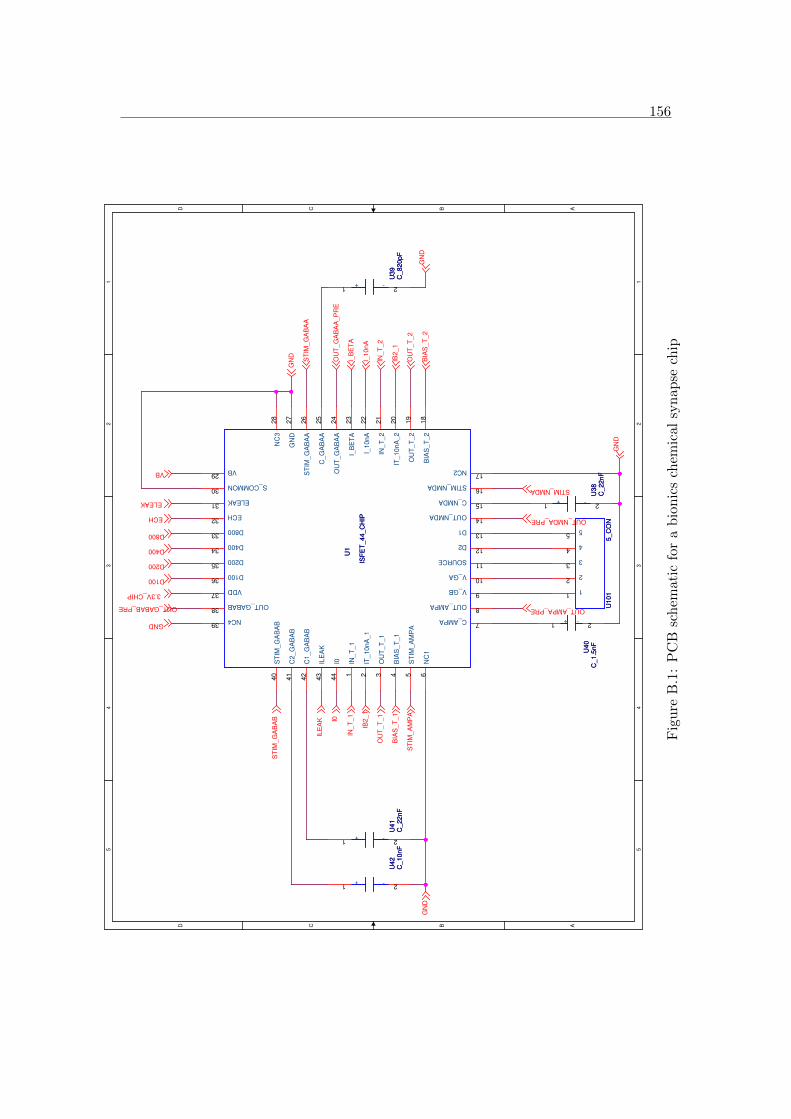
1565 5
4 4
3 3
2 2
1 1
DD
CC
BB
AA
GN
D
3.3V_CHIP
OUT_AMPA_PRE
OUT_NMDA_PRE
OU
T_G
AB
AA
_P
RE
OUT_GABAB_PRE
ELEAK
ECH
VB
GND
GN
D
I_10nA
I_B
ET
A
ST
IM_A
MP
A
STIM_NMDA
ST
IM_G
AB
AA
ST
IM_G
AB
AB
ILE
AK I0
GN
D
GN
D
D100
D200
D400
D800
IB2_1
IB2_1
OU
T_T
_1
OU
T_T
_2
BIA
S_T
_1
BIA
S_T
_2
IN_T
_1
IN_T
_2
U101
5_C
ON
U101
5_C
ON
11
22
33
44
55
U41
C_22nF
U41
C_22nF
+1
-2
U1
ISF
ET
_44_C
HIP
U1
ISF
ET
_44_C
HIP
C_AMPA7
OUT_AMPA8
V_GB9
V_GA10
SOURCE11
D212
D113
OUT_NMDA14
C_NMDA15
STIM_NMDA16
NC217
BIA
S_T
_2
18
OU
T_T
_2
19
IT_10nA
_2
20
IN_T
_2
21
I_10nA
22
I_B
ET
A23
OU
T_G
AB
AA
24
C_G
AB
AA
25
ST
IM_G
AB
AA
26
GN
D27
NC
328
VB29
S_COMMON30
ELEAK31
ECH32
D80033
D40034
D20035
D10036
VDD37
OUT_GABAB38
NC439
ST
IM_G
AB
AB
40
C2_G
AB
AB
41
C1_G
AB
AB
42
ILE
AK
43
I044
IN_T
_1
1
IT_10nA
_1
2
OU
T_T
_1
3
BIA
S_T
_1
4
ST
IM_A
MP
A5
NC
16
U38
C_22nF
U38
C_22nF
+1
-2
U39
C_820pF
U39
C_820pF
+1
-2
U40
C_1.5
nF
U40
C_1.5
nF
+1
-2
U42
C_10nF
U42
C_10nF
+1
-2
Fig
ure
B.1
:P
CB
sch
emat
icfo
ra
bio
nic
sch
emic
alsy
nap
sech
ip

1575 5
4 4
3 3
2 2
1 1
DD
CC
BB
AA
GN
D
OU
T_A
MP
A
OU
T_N
MD
A
GN
D
OU
T_G
AB
AA
GN
D
OU
T_G
AB
AB
GN
D
ELE
AK
EC
H
GN
DG
ND
VB
GN
D
OU
T_G
AB
AB
_P
RE
OU
T_G
AB
AA
_P
RE
OU
T_N
MD
A_P
RE
OU
T_A
MP
A_P
RE
GN
D
OU
T_A
MP
A
GN
D
OU
T_N
MD
A
GN
D
GN
D
OU
T_G
AB
AA
OU
T_G
AB
AB
+6V
+6V
+6V
+6V
OU
T_A
MP
A_P
RE
OU
T_N
MD
A_P
RE
OU
T_G
AB
AA
_P
RE
OU
T_G
AB
AB
_P
RE
GN
D
GN
D
GN
D
GN
D
Buffer of output signal
Unbuffer of output signal
U99
BN
C
U99
BN
C
SIG
1
G1
2
G2
3
G3
4
G4
5
U19
SM
AU
19
SM
A
SIG
1G
12
G2
3
G3
4
G4
5
U6
BN
C
U6
BN
C
SIG
1
G1
2
G2
3
G3
4
G4
5
U3
SM
A
U3
SM
A
SIG
1G
12
G2
3
G3
4
G4
5
U77
LM
C6001
U77
LM
C6001
BC11
-2
+3
GND4
BC35
OU
T6
VCC7
C28
U70
Test_
Poin
t
U70
Test_
Poin
t
1
U72
Test_
Poin
t
U72
Test_
Poin
t
1
U14
BN
C
U14
BN
C
SIG
1
G1
2
G2
3
G3
4
G4
5
U11
SM
A
U11
SM
A
SIG
1G
12
G2
3
G3
4
G4
5
U10
BN
C
U10
BN
C
SIG
1
G1
2
G2
3
G3
4
G4
5
U12
BN
C
U12
BN
C
SIG
1
G1
2
G2
3
G3
4
G4
5
U18
BN
C
U18
BN
C
SIG
1
G1
2
G2
3
G3
4
G4
5
U36
BN
C
U36
BN
C
SIG
1
G1
2
G2
3
G3
4
G4
5
U37
BN
C
U37
BN
C
SIG
1
G1
2
G2
3
G3
4
G4
5
U73
Test_
Poin
t
U73
Test_
Poin
t
1
U76
LM
C6001
U76
LM
C6001
BC11
-2
+3
GND4
BC35
OU
T6
VCC7
C28
U74
Test_
Poin
t
U74
Test_
Poin
t
1
U78
LM
C6001
U78
LM
C6001
BC11
-2
+3
GND4
BC35
OU
T6
VCC7
C28
U75
LM
C6001
U75
LM
C6001
BC11
-2
+3
GND4
BC35
OU
T6
VCC7
C28
U7
SM
A
U7
SM
A
SIG
1G
12
G2
3
G3
4
G4
5
U13
SM
A
U13
SM
A
SIG
1G
12
G2
3
G3
4
G4
5
U9
SM
A
U9
SM
A
SIG
1G
12
G2
3
G3
4
G4
5
U17
BN
C
U17
BN
C
SIG
1
G1
2
G2
3
G3
4
G4
5
U69
Test_
Poin
t
U69
Test_
Poin
t
1
U15
SM
AU
15
SM
A
SIG
1G
12
G2
3
G3
4
G4
5
U68
Test_
Poin
t
U68
Test_
Poin
t
1
U2
BN
C
U2
BN
C
SIG
1
G1
2
G2
3
G3
4
G4
5
U71
Test_
Poin
t
U71
Test_
Poin
t
1
U8
BN
C
U8
BN
C
SIG
1
G1
2
G2
3
G3
4
G4
5
Fig
ure
B.2
:P
CB
sch
emat
icfo
rth
eO
PA
MP
bu
ffer
and
BN
C,
SM
Ap
orts

1585 5
4 4
3 3
2 2
1 1
DD
CC
BB
AA
GN
D
GN
D
I_10nA
I_B
ET
A
GN
D
GN
D
ILE
AK
I0
IB2_1
IB2_1
GN
D
GN
D
GN
D
BIA
S_T
_1
GN
D
BIA
S_T
_2
D100
D200
D400
D800
GN
D
IN_T
_1
IN_T
_2
GN
D
Current sink (positive value)
Ib2 (10nA bias)
VREF to source of ISFET and BIAS_T
Ib1 (Bias current for ref. elec)
IN_T1,2 to
drain of
ISFET
U22
BN
C
U22
BN
C
SIG
1
G1
2
G2
3
G3
4
G4
5
U105
Test_
Poin
t
U105
Test_
Poin
t
1
U109
Test_
Poin
t
U109
Test_
Poin
t
1
U23
SM
AU
23
SM
A
SIG
1G
12
G2
3
G3
4
G4
5
U46
JU
MP
ER
2U
46
JU
MP
ER
2
SIG
11
SIG
22
U64
BN
C
U64
BN
C
SIG
1
G1
2
G2
3
G3
4
G4
5
U45
JU
MP
ER
2U
45
JU
MP
ER
2
SIG
11
SIG
22
U50
SM
AU
50
SM
A
SIG
1G
12
G2
3
G3
4
G4
5
U114
Test_
Poin
tU
114
Test_
Poin
t
1
U44
JU
MP
ER
2U
44
JU
MP
ER
2
SIG
11
SIG
22
U100
BN
C
U100
BN
C
SIG
1
G1
2
G2
3
G3
4
G4
5U
43
JU
MP
ER
2U
43
JU
MP
ER
2
SIG
11
SIG
22
U25
SM
AU
25
SM
A
SIG
1G
12
G2
3
G3
4
G4
5
U24
BN
C
U24
BN
C
SIG
1
G1
2
G2
3
G3
4
G4
5
U110
Test_
Poin
t
U110
Test_
Poin
t
1U
47
BN
C
U47
BN
C
SIG
1
G1
2
G2
3
G3
4
G4
5
U49
BN
C
U49
BN
C
SIG
1
G1
2
G2
3
G3
4
G4
5
U48
SM
AU
48
SM
A
SIG
1G
12
G2
3
G3
4
G4
5
U104
Test_
Poin
t
U104
Test_
Poin
t
1U
65
BN
C
U65
BN
C
SIG
1
G1
2
G2
3
G3
4
G4
5
U67
BN
C
U67
BN
C
SIG
1
G1
2
G2
3
G3
4
G4
5
U106
Test_
Poin
t
U106
Test_
Poin
t
1
U66
BN
C
U66
BN
C
SIG
1
G1
2
G2
3
G3
4
G4
5
U62
BN
C
U62
BN
C
SIG
1
G1
2
G2
3
G3
4
G4
5
U111
Test_
Poin
t
U111
Test_
Poin
t
1
U58
BN
C
U58
BN
C
SIG
1
G1
2
G2
3
G3
4
G4
5
U21
SM
AU
21
SM
A
SIG
1G
12
G2
3
G3
4
G4
5
U103
Test_
Poin
t
U103
Test_
Poin
t
1
U20
BN
C
U20
BN
C
SIG
1
G1
2
G2
3
G3
4
G4
5
U63
BN
C
U63
BN
C
SIG
1
G1
2
G2
3
G3
4
G4
5
U108
Test_
Poin
t
U108
Test_
Poin
t
1
U107
Test_
Poin
tU
107
Test_
Poin
t
1
U4
SM
A
U4
SM
A
SIG
1G
12
G2
3
G3
4
G4
5
U102
Test_
Poin
tU
102
Test_
Poin
t
1
U35
SM
AU
35
SM
A
SIG
1G
12
G2
3
G3
4
G4
5
U34
BN
C
U34
BN
C
SIG
1
G1
2
G2
3
G3
4
G4
5
Fig
ure
B.3
:P
CB
sch
emat
icfo
rth
eB
NC
,S
MA
por
tsI
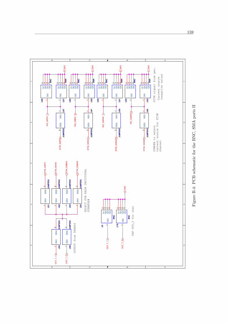
1595 5
4 4
3 3
2 2
1 1
DD
CC
BB
AA
ST
IM_A
MP
A
ST
IM_N
MD
A
ST
IM_G
AB
AA
ST
IM_G
AB
AB
OU
T_T
_1
OU
T_T
_2
SIG
_A
MP
A
SIG
_G
AB
AB
SIG
_N
MD
A
SIG
_G
AB
AA
GN
D
GN
D
GN
D
GN
D
ST
IM_A
MP
A
ST
IM_N
MD
A
ST
IM_G
AB
AA
ST
IM_G
AB
AB
OU
T_T
_1
OU
T_T
_2
GN
D
OUTPUT from TRANS4
SELECT FOR EACH INDIVIDUAL
SYNAPSE#
JUMPER to select
current source for STIM
channel
STIM signal from gen.
Current source
(negative value)
TAP OUT_T for char
U55
JU
MP
ER
2U
55
JU
MP
ER
2
SIG
11
SIG
22
U26
BN
C
U26
BN
C
SIG
1
G1
2
G2
3
G3
4
G4
5
U29
SM
AU
29
SM
A
SIG
1G
12
G2
3
G3
4
G4
5
U33
SM
AU
33
SM
A
SIG
1G
12
G2
3
G3
4
G4
5U
60
JU
MP
ER
2U
60
JU
MP
ER
2
SIG
11
SIG
22
U57
JU
MP
ER
2U
57
JU
MP
ER
2
SIG
11
SIG
22
U54
JU
MP
ER
2U
54
JU
MP
ER
2
SIG
11
SIG
22
U53
JU
MP
ER
2U
53
JU
MP
ER
2
SIG
11
SIG
22
U52
JU
MP
ER
2U
52
JU
MP
ER
2
SIG
11
SIG
22
U5
BN
C
U5
BN
C
SIG
1
G1
2
G2
3
G3
4
G4
5
U28
BN
C
U28
BN
C
SIG
1
G1
2
G2
3
G3
4
G4
5
U51
JU
MP
ER
2U
51
JU
MP
ER
2
SIG
11
SIG
22
U27
SM
AU
27
SM
A
SIG
1G
12
G2
3
G3
4
G4
5
U31
SM
AU
31
SM
A
SIG
1G
12
G2
3
G3
4
G4
5
U32
BN
C
U32
BN
C
SIG
1
G1
2
G2
3
G3
4
G4
5
U61
JU
MP
ER
2U
61
JU
MP
ER
2
SIG
11
SIG
22
U16
BN
C
U16
BN
C
SIG
1
G1
2
G2
3
G3
4
G4
5
U30
BN
C
U30
BN
C
SIG
1
G1
2
G2
3
G3
4
G4
5
U59
JU
MP
ER
2U
59
JU
MP
ER
2
SIG
11
SIG
22
U56
JU
MP
ER
2U
56
JU
MP
ER
2
SIG
11
SIG
22
Fig
ure
B.4
:P
CB
sch
emat
icfo
rth
eB
NC
,S
MA
por
tsII