Embed Size (px)
Citation preview
Article No. sm980595Superlattices and Microstructures, Vol. 24, No. 5, 1998
Binding energies of excitons in symmetric and asymmetric quantumwells in a magnetic field
E. KASAPOGLU, H. SARI, Y. ERGUN, S. ELAGOZ
Cumhuriyet University, Physics Department, 58140 Sivas-Turkey
I. SOKMEN
Dokuz Eylul University, Physics Department,Izmir-Turkey
(Received 30 June 1998)
The binding energy of the exciton in the symmetric and asymmetric GaAs/Ga1−xAl xAsquantum wells is calculated with the use of a variational approach. Results have been ob-tained as a function of the potential symmetry, and the size of the quantum well in thepresence of an arbitrary magnetic field. The applied magnetic field is taken to be parallel tothe axis of growth of the quantum well structure. The role of the asymmetric barriers, mag-netic field, and well width in the excitonic binding is discussed as the tunability parametersof the GaAs/Ga1−xAl xAs system.
c© 1998 Academic PressKey words: exciton binding, asymmetric quantum well, magnetic field.
1. Introduction
With recent developments in low-dimensional systems, the electromagnetic properties of an electron gasconfined in a quantum well semiconductor heterostructure have attracted wide attention due to the possibilityin high-performance electronics of tunneling devices. The quantum devices usually studied may consist of asingle barrier, a quantum well or double barrier or multiple quantum well structures. These quantum devicesare commonly taken to be symmetric, but the asymmetric quantum devices give new tunable properties whichare very important for device applications [1–8]. The research on the linear and nonlinear optical propertiesof semiconductors has further been stimulated by the increasing number of applications of the semiconductordiode laser and optoelectronic components in communications and consumer electronics. The main advantageof the GaAs/Ga1−xAl xAs system is the combination of large optical nonlinearities and the direct band gap,which leads to very efficient radiative recombination of carriers [9]. These physical properties are essentialfor the operation of very fast optical switches.
Due to the improved qualities of the heterojunction devices, a practical sample with asymmetric potentialconfiguration can be fabricated by using differentx parameters in Ga1−xAl xAs to achieve a different potentialbarrier height in a quantum well structure. In particular, the theoretical problems of excitons in low-dimensionalsystems subject to a magnetic and an electric field has been treated by a number of authors [10–22].
0749–6036/98/050359 + 10 $30.00/0 c© 1998 Academic Press

360 Superlattices and Microstructures, Vol. 24, No. 5, 1998
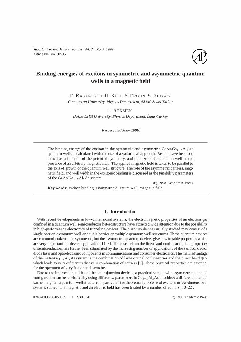
Ga1–xAlxAs–b Ga1–xAlxAsGaAsC
z
B
V
VReVL
e
VLh VR
h
–b b
Fig. 1. Schematic band diagram of a GaAs/Ga1−xAl xAs quantum well and the applied magnetic fieldB in the growth direction. Thevalues of the physical parameters are given in the text.
The study of the electronic structure of an electron in low-dimensional structures is therefore of considerableinterest and will be helpful in realizing the optical properties, transport phenomena, and quantum effects ofthe quantum devices with different potential configurations. Recently, a large number of experimental studieson the optical properties of wide-gap compound semiconductor quantum wells has appeared in the literature.In these materials, usually strong exciton effects have been measured [23–27].
The aim of the present paper is to study the role of the potential symmetry, magnetic field and well widthin the excitonic binding in quantum wells with finite potential barriers. We use a variational approach andsubband mixing is ignored. Since the potential barriers are finite, the electron and hole can penetrate intothe barriers, therefore the transition of the exciton from three dimensions to two dimensions is predicted. Wewill show that in the range of the well width, where the exciton has a two-dimensional character, the bindingenergy is very sensitive to the magnetic field and well width values.
Also, we have calculated the overlap functionF(0) as a function of the well width between the electronand hole to describe the exciton behavior in asymmetric quantum wells. Although several authors have donea considerable amount of work on the properties of excitons in quantum wells, to our knowledge, the effectsof a magnetic field on asymmetric quantum wells have not been theoretically studied.
2. Theory
We consider a quantum well (QW) consisting of a GaAs layer sandwiched between two semi-infiniteGa1−xAl xAs slabs. The conduction and valence band of this system is given schematically in Fig. 1. Auniform magnetic fieldB is applied perpendicular to the layers. In this paper, the effect of the magnetic field,the well width and the barrier ratio of an asymmetric quantum well is taken into consideration to describe theproperties of the excitonic binding in the ground state.
In the framework of the effective mass approximation, the Hamiltonian of the electron-hole system is
H = 1
2me
[Pe+ e
cA(re)
]2+ 1
2mh
[Ph − e
cA(rh)
]2− e2
ε0|re− rh| + Ve(ze)+ Vh(zh) (1)
whereVe(ze) andVh(zh) are the confinement potential profiles for the electrons and holes in thez-direction,respectively,A = 1
2(B× r) is the vector potential of the magnetic fieldB, ε0 is the dielectric constant of thesystem,re andrh are the electron and hole positions. The functional form of the confinement potentials are

Superlattices and Microstructures, Vol. 24, No. 5, 1998 361
the following
Ve(ze) =
VeL , ze < −L/2
0, −L/2< ze < L/2Ve
R, ze > L/2
Vh(zh) =Vh
L , zh < −L/20, −L/2< zh < L/2Vh
R, zh > L/2
with left VeL , Vh
L and rightVeR, Vh
R potentials of confinement. Here we have chosen the origin of the coordinate
system to be the center of the GaAs well. In the asymmetric case, we takeV (e,h)R /V (e,h)
L 6= 1. In ourcalculation in order to describe the ratio of the right confinement potential to the left one, we define theparameterσ = V (e,h)
R /V (e,h)L .
In our expression for the exciton Hamiltonian we have assumed the same values for the conduction andvalence band mass parameters and the static dielectric constant in GaAs and Ga1−xAl xAs. For the mostcommonly used values ofx, these physical parameters are not too different in the two materials [28]. As thedielectric constants of two semiconductors are nearly equal, the image force effect is neglected in the presentcalculation.
It is convenient to introduce the center-of-mass coordinateR = (mere+mhrh)/M , M = me+mh, andrelative coordinater = re− rh:
H = − h2
2µ
(∂2
∂x2 +∂2
∂y2
)− h2
2µ
∂2
∂z2 +ehB
2µc
(mh
M− me
M
)Lz+ e2
2µc2
1
4B2(x2+ y2)
− e2
ε0|r| + Ve(ze)+ Vh(zh) (2)
whereµ = memh/M is the reduced mass in the (x–y) plane andLz is the z-component of the angularmomentum operator (in unitsh = 1).
By using cylindrical coordinatesx = ρ cosφ, y = ρ sinφ, we obtained the Hamiltonian as follows.
H = − h2
2µ
[∂2
∂ρ2 +1
ρ
∂
∂ρ+ ∂2
∂φ2
]− h2
2µ
∂2
∂z2 +ehB
2µcLz
(mh
M− me
M
)+ e2
2µc2
1
4B2ρ2
− e2
ε0√ρ2+ (ze− zh)2
+ Ve(ze)+ Vh(zh) (3)
whereρ = √(xe− xh)2+ (ye− yh)2 is the relative distance between the electron and hole in thex–y plane.We then scale all lengths in the exciton Bohr radiusaB = ε0h2/µe2, and energies in the exciton Rydberg
R= µe4/2ε20h2, to obtain the dimensionless form of the Hamiltonian
H = −[
1
ρ
∂
∂ρρ∂
∂ρ+ 1
ρ2
∂2
∂φ2
]− µ
me
∂
∂ z2e− µ
mh
∂
∂ z2h
+(mh
M− me
M
)γ Lz+ 1
4γ 2ρ2
− 2√ρ2+ (ze− zh)2
+ Ve(ze)+ Vh(zh) (4)
whereγ is the first Landau level expressed inR, γ = ehB/2µcR. The HamiltonianH can be split into threeterms: the electron partHe(ze), the hole partHh(zh), and the exciton partHex(ρ, φ),
H(ρ, φ, ze, zh) = He(ze)+ Hh(zh)+ Hex(ρ, φ, ze, zh),

362 Superlattices and Microstructures, Vol. 24, No. 5, 1998
20
16
12
EB(m
eV)
8
40 50 100
L (Å)
150 200
B=200 kGB=150 kG
B=100 kG
B=50 kG
B=10 kG
B=0
σ = 1
Fig. 2. Variation of the binding energy of the exciton as a function of the well widthL, for several values of the magnetic field in thesymmetric quantum well.
where
He(ze) = − µme
∂
∂ z2e+ Ve(ze)
Hh(zh) = − µ
mh
∂
∂ z2h
+ Vh(zh) (5)
Hex = −[
1
ρ
∂
∂ρρ∂
∂ρ+ 1
ρ2
∂2
∂φ2
]+(mh
M− me
M
)γ Lz+ 1
4γ 2ρ2− 2√
ρ2+ (ze− zh)2.
The wavefunction8 = ψle(ze)ψlh(zh)ϕ(ρ, α) of the electron–hole system is solved from the Schr¨odingerequation,
H(ρ, φ, ze, zh)8(ρ, φ, ze, zh) = E8(ρ, φ, ze, zh) (6)
whereE is the total energy,ψle(ze) andψlh(zh) represents the motion of the electron and hole in thel th statein z-direction, respectively. The motion of exciton in the (x–y) plane is described by the wavefunction of theground state of a two-dimensional hydrogen-like atom:
ϕ(ρ, α) =√
2
π
1
αexp[−ρ/α] (7)
whereα is treated as a variational parameter. We next evaluate the expectation value
E = 〈8|H |8〉 (8)
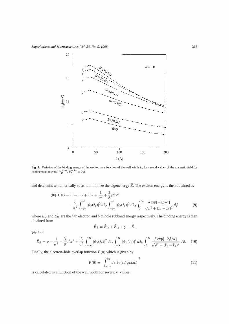
Superlattices and Microstructures, Vol. 24, No. 5, 1998 363
20
16
12
EB(m
eV)
8
40 50 100
L (Å)
150 200
B=200 kGB=150 kG
B=100 kG
B=50 kG
B=10 kG
B=0
σ = 0.8
Fig. 3. Variation of the binding energy of the exciton as a function of the well widthL, for several values of the magnetic field for
confinement potentialV (e,h)R /V (e,h)L = 0.8.
and determineα numerically so as to minimize the eigenenergyE. The exciton energy is then obtained as
〈8|H |8〉 = E = Ele + Elh + 1
α2 +3
8γ 2α2
− 8
α2
∫ ∞−∞|ψe(ze)|2 dze
∫ ∞−∞|ψe(ze)|2 dzh
∫ ∞0
ρ exp[−2ρ/α]√ρ2+ (ze− zh)2
dρ (9)
whereEle andElh are theleth electron andlhth hole subband energy respectively. The binding energy is thenobtained from
EB = Ele + Elh + γ − E.
We find
EB = γ − 1
α2 −3
8γ 2α2+ 8
α2
∫ ∞−∞|ψe(ze)|2 dze
∫ ∞−∞|ψh(zh)|2 dzh
∫ ∞0
ρ exp[−2ρ/α]√ρ2+ (ze− zh)2
dρ. (10)
Finally, the electron–hole overlap functionF(0) which is given by
F(0) =∣∣∣∣ ∫ ∞−∞ dzψe(ze)ψh(zh)
∣∣∣∣2 (11)
is calculated as a function of the well width for severalσ values.

364 Superlattices and Microstructures, Vol. 24, No. 5, 1998
20
16
12
EB(m
eV)
8
40 40 80
L (Å)
120 200160
B=200 kGB=150 kG
B=100 kG
B=50 kG
B=10 kG
B=0
σ = 0.5
Fig. 4. Variation of the binding energy of the exciton as a function of the well widthL, for several values of the magnetic field for
confinement potentialV (e,h)R /V (e,h)L = 0.5.
3. Results and discussion
In this study we have calculated the exciton binding energy associated with the electron and hole firstsubbands (le = 1, lh = 1) as a function of the field strength of magnetic field, well width, and the confinementpotential ratiosσ .
For the numerical calculations, we takeme = 0.067m0, mh = 0.45m0, ε0 = 12.5, aB = 165.591 Å,R = 3.47369 meV,Ve
L = 228 meV,VhL = 176 meV. These parameters are suitable for GaAs/Ga1−xAl xAs
heterostructures with the Al concentrationx ∼= 0.3. We have assumed the conduction-band discontinuity tobe 56% of the total band-gap difference, which has recently been suggested as a more appropriate value [28].Firstly we have considered the symmetric QW(σ = 1) for both electron and hole.
The values of the binding energiesEB of the exciton as a function ofL for several values of the magneticfield are displayed in Fig. 2. For comparison, we also show the variation ofEB with L for a zero magneticfield. As expected due to the greater confinement, the presence of a magnetic field leads to more binding. Forvery largeL values, the excitonic binding approaches a three-dimensional hydrogen-like system, since in thewide wells the probability of finding the electron and hole in the same plane is very small. The binding energyof the exciton increases asL is reduced until it reaches a maximum and then decreases quite rapidly. ForLvalues where the binding energy is maximal the system has quasi two-dimensional character and the overlapfunctionF(0) between the electron and hole is maximal (see Fig. 6). As seen in Fig. 2 the value ofL at whichthe binding energy reaches a maximum is about the same for all values of the magnetic field, and, due to the

Superlattices and Microstructures, Vol. 24, No. 5, 1998 365
16
12
8
EB(m
eV)
40 50 100
L (Å)
150 200
B=200 kGB=150 kG
B=100 kG
B=50 kG
B=10 kG
B=0
σ = 0.3
Fig. 5. Variation of the binding energy of the exciton as a function of the well widthL, for several values of the magnetic field for
confinement potentialV (e,h)R /V (e,h)L = 0.3.
greater confinement of the electron and hole at largeB values, the excitonic binding is more sensitive to thewell width L, and decreases sharply with increasing well width. At larger well widths the extension of thewavefunction in the (x–y) plane increases; and this increases the contribution of the magnetic term of theHamiltonian which is proportional toγ 2ρ2 (eqn (4)). The increment of this positive term gives a decrease inthe excitonic binding energy.
It also should be pointed out that at very small well widths the penetration of the electron and hole increases,since particles become more energetic, thus the system has a three dimensional character. As seen in Fig. 2 atsmall L values the binding energy approaches the three-dimensional hydrogen-like system.
Now let us consider exciton properties in asymmetric quantum wells. In Fig. 3 we show the exciton bindingenergy curves by using right and left confinement potentials withσ = 0.8 for differentB values. While forlarge well widths the binding energy shows a similar behavior as that in symmetric QWs, for small well widthsthe trend is more complicated showing secondary decreasing in the curves due to dimensional transition. Asthe well widthL decreases, the exciton binding energy increases towards the two-dimensional limit. But asL becomes smaller, the energetic and light particle electron begins to penetrate into the barrier. Due to theloss of localization of the electron the binding energy decreases. However, since the less energetic and heavyparticle is still bounded (localized) in the well the decrease in the binding energy is not very sharp. Also,as L becomes smaller and smaller the hole delocalizes into the barrier, the decrease in the binding energybegins to sharpen and the exciton completely recovers its three-dimensional behavior, as a result the secondarydecreasing occurs in the curves. Therefore we conclude that in asymmetric QWs delocalization of the electronand hole occurs at different well-width values. This behavior is clearly seen in Fig. 3 for largeB values.
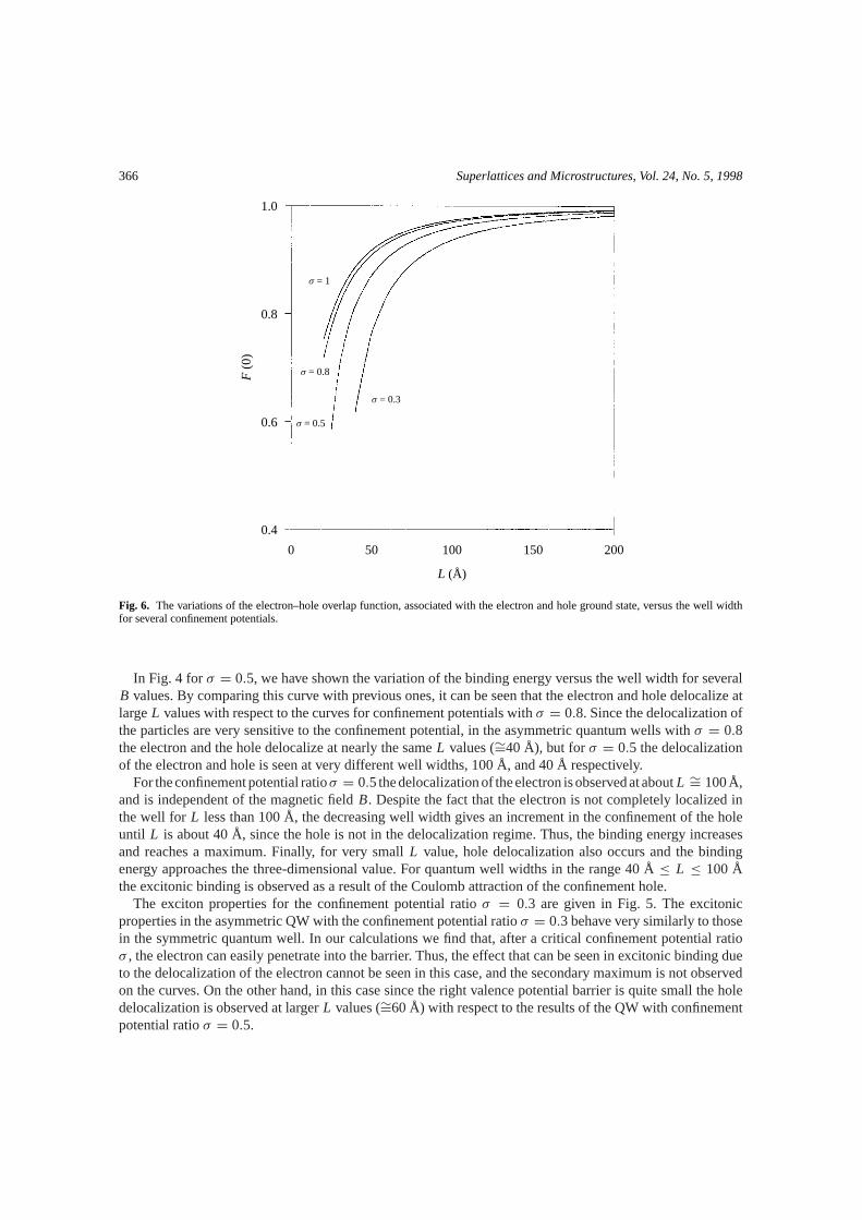
366 Superlattices and Microstructures, Vol. 24, No. 5, 1998
1.0
0.8
0.6
F (
0)
0.4
0 50 100
L (Å)
150 200
σ = 0.8
σ = 1
σ = 0.5
σ = 0.3
Fig. 6. The variations of the electron–hole overlap function, associated with the electron and hole ground state, versus the well widthfor several confinement potentials.
In Fig. 4 forσ = 0.5, we have shown the variation of the binding energy versus the well width for severalB values. By comparing this curve with previous ones, it can be seen that the electron and hole delocalize atlargeL values with respect to the curves for confinement potentials withσ = 0.8. Since the delocalization ofthe particles are very sensitive to the confinement potential, in the asymmetric quantum wells withσ = 0.8the electron and the hole delocalize at nearly the sameL values (∼=40 Å), but forσ = 0.5 the delocalizationof the electron and hole is seen at very different well widths, 100 Å, and 40 Å respectively.
For the confinement potential ratioσ = 0.5 the delocalization of the electron is observed at aboutL ∼= 100 Å,and is independent of the magnetic fieldB. Despite the fact that the electron is not completely localized inthe well for L less than 100 Å, the decreasing well width gives an increment in the confinement of the holeuntil L is about 40 Å, since the hole is not in the delocalization regime. Thus, the binding energy increasesand reaches a maximum. Finally, for very smallL value, hole delocalization also occurs and the bindingenergy approaches the three-dimensional value. For quantum well widths in the range 40 Å≤ L ≤ 100 Åthe excitonic binding is observed as a result of the Coulomb attraction of the confinement hole.
The exciton properties for the confinement potential ratioσ = 0.3 are given in Fig. 5. The excitonicproperties in the asymmetric QW with the confinement potential ratioσ = 0.3 behave very similarly to thosein the symmetric quantum well. In our calculations we find that, after a critical confinement potential ratioσ , the electron can easily penetrate into the barrier. Thus, the effect that can be seen in excitonic binding dueto the delocalization of the electron cannot be seen in this case, and the secondary maximum is not observedon the curves. On the other hand, in this case since the right valence potential barrier is quite small the holedelocalization is observed at largerL values (∼=60 Å) with respect to the results of the QW with confinementpotential ratioσ = 0.5.

Superlattices and Microstructures, Vol. 24, No. 5, 1998 367
Finally, we display in Fig. 6 the overlap functionF(0) between the electron and the hole as a function ofthe well width L for several confinement potentials. For very large well widths the overlap functionF(0)is not sensitive to the confinement potential ratios. In the quantum well with a very large width the bandoffsets act on the particles as infinite potential barriers, and the electron and hole wavefunctions are identical.Consequently, as expected, when the well width goes to infinity the probability of finding the electron andhole in the same plane becomes very large, thusF(0) goes to unity.
Summarizing, theoretical investigations of the excitonic properties of asymmetric quantum wells have beenpresented. The work focused on the symmetry dependence of the electron and hole confinement, electron–holecoupling and excitonic binding in the quantum well under a magnetic field applied in the growth direction.The method used in the present work is capable of describing the correct behavior of excitons, and the effectof a magnetic field on the excitonic structure in asymmetric quantum wells. Calculated results reveal that,using a heterostructure one can tailor the energy band structure by an appropriate layer sequence whichmay improve the mechanism for light-induced modification of the band structure, obtaining even, enhanced,nonlinear optical properties. This results in an improvement in optoelectronic devices. We also conclude that,in asymmetric heterostructures, the changes in excitonic binding energy and oscillator strengths are largerthan the changes that occur in conventional square potential wells and are strongly dependent on the strengthof the magnetic field, and the symmetry of the quantum wells. This added degree of freedom yields uniqueproperties that may have applications in switching devices.
References
[1] }}W. Q. Chen and T. G. Anderson, Semicond. Sci. Technol.7, 828 (1992).[2] }}W. Q. Chen and T. G. Anderson, Appl. Phys. Lett.60, 1591 (1992).[3] }}G. Sanders and K. K. Bajaj, J. Appl. Phys.68, 5348 (1990).[4] }}M. Morita, K. Goto, and T. Suziki, Jpn. Appl. Phys.29, L1663 (1990).[5] }}H. Kroemer and H. Okamoto, Jpn. J. Appl. Phys.23, 970 (1984).[6] }}E. J. Austin and M. Jaros, J. Phys.C19, 533 (1986).[7] }}P. Yuh and K. L. Wang, Phys. Rev.B38, 8377 (1988).[8] }}H. Sari, I. Sokmen, Y. Ergun, S. Elagoz, E. Kasapoglu, and M. Tomak, Superlatt. Microstruct.23, 1067
(1998).[9] }}H. Haug,Optical Nonlinearities and Instabilities in Semiconductors(Academic Press, San Diego, 1988).
[10] }}U. Ekenberg, Phys. Rev.B40, 7714 (1989).[11] }}H. L. Cui and N. J. M. Horing, Phys. Rev.B40, 2901 (1989).[12] }}M. Shayegan, T. Sajoto, J. Jo, M. Santos, and H. D. Drew, Phys. Rev.B40, 3476 (1989).[13] }}M. P. Stopa and S. Das Sarma, Phys. Rev.B40, 10048 (1989).[14] }}T. Uenoyama and L. J. Sham, Phys. Rev.B39, 11044 (1989).[15] }}B. Huckestein and R. K¨ummel, Phys. Rev.B38, 8215 (1989).[16] }}G. Brozak, B. D. McCombe, and D. M. Larsen, Phys. Rev.B40, 1265 (1989).[17] }}Yun Zhu, Hao Chen, and Shixun Zhou, Phys. Rev.B38, 4283 (1988).[18] }}H. Q. Hou, Y. Segawa, Y. Aoyagi, S. Namba, and J. M. Zhou, Phys. Rev.B42, 1284 (1990).[19] }}W. Trzeciakowski, J. Appl. Phys.66, 4780 (1989).[20] }}A. B. Henriques and E. C. Valadares, Superlatt. Microstruct.10, 187 (1991).[21] }}K. M. Hung and G. Y. Wu, Solid State Commun.80, 367 (1991).[22] }}H. R. Lee, H. G. Oh, Thomas F. George, and C. I. Um. J. Appl. Phys.66, 2442 (1989).[23] }}G. Platero and M. Altarelli, inProceedings of 20th International Conference on the Physics of Semi-
conductors, edited by E. M. Anastassakis and J. D. Joannopoulos (World Scientific, Singapore, 1990),p. 83.
368 Superlattices and Microstructures, Vol. 24, No. 5, 1998
[24] }}H. Tuffigo, R. T. Cox, N. Magnea, Y. Merle d’Aubigne, and A. Million, Phys. Rev.B37, 4310 (1988);H. Tuffigo, N. Magnea, H. Mariette, A. Wasiela, and Y. Merle d’Aubigne, Phys. Rev.B43, 14629 (1991).
[25] }}A. D’ Andrea, R. Del Sole, and K. Cho, Europhys. Lett.11, 169 (1990).[26] }}G. R. Pozina, A. V. Kavokin, V. P. Kocheroshko, Uraltsev, D. R. Yakovlev, G. Landwehr, R. N. Bicknell-
Tassius, and A. Waag, Solid State Commun.81, 639 (1992).[27] }}A. D’Andrea, R. Del Sole, and N. Tomassini, inProceedings of the First Italian Workshop on Materials
for Photonic Devices, edited by A. D’Andrea, A. Lapiccirella, G. Marletta, and S. Viticoli (WorldScientific, Singapore, 1991), p. 185.
[28] }}H. J. Lee, L. Y. Juravel, J. C. Wolley, and A. J. Springthorpe, Phys. Rev.B21, 659 (1980).[29] }}R. C. Miller, A. C. Gossard, D. A. Kleinman, and O. Munteanu, Phys. Rev.B29, 3740 (1984).